25. XSPI I/O manager (XSPIM)
25.1 XSPIM introduction
The XSPI I/O manager is a low-level interface, enabling an efficient XSPI pin assignment with a full I/O matrix (before alternate function map), and multiplex of single/dual/quad/octal/16-bit SPI interfaces over the same bus.
25.2 XSPIM main features
- • Supports up to two single/dual/quad/octal/16-bit SPI interfaces
- • Supports up to two ports for pin assignment
- • Supports high-speed interfaces
25.3 XSPIM implementation
Table 216 describes the XSPIM implementation.
Table 216. XSPIM implementation
| XSPI feature | Available on the devices |
|---|---|
| Supports up to two single/dual/quad interfaces | X |
| Fully I/O multiplexing capability | X |
| Supports time-multiplexed mode | X |
| Supports high-speed interface | X |
| Chip select selection if XSPI provides dual chip select | X |
| Supports 16-bit data interface and dual-octal mode | X |
25.4 XSPIM functional description
25.4.1 XSPIM block diagram
The block diagram of the XSPI I/O manager is shown in Figure 214 .
Figure 214. XSPIM block diagram
![XSPIM block diagram showing internal components like AHB interface, Control register, Static muxing, I/O matrix, and PHY, connected to external pins such as XSPIM_P1_CLK, XSPIM_P1_NCLK, XSPIM_P1_DQS0,1, XSPIM_P1_NCS1,2, XSPIM_P1_IO[15:0], XSPIM_P2_CLK, XSPIM_P2_NCLK, XSPIM_P2_DQS0, XSPIM_P2_NCS1,2, XSPIM_P2_IO[7:0].](/RM0477-STM32H7Rx-7Sx/363909ecac21a926290075a4debc8c6a_img.jpg)
The diagram illustrates the internal architecture of the XSPIM. It features an AHB interface connected to an AHB bus. A control register is also connected to the AHB. Below these, an XSPI1 and XSPI2 block are shown, connected to the internal bus signals. An arbiter and time muxing blocks are present between the XSPI blocks and the I/O matrix. The I/O matrix is divided into Port 1 and Port 2, which are then connected to PHY blocks. The PHY blocks are connected to the external pins: XSPIM_P1_CLK, XSPIM_P1_NCLK, XSPIM_P1_DQS0,1, XSPIM_P1_NCS1,2, XSPIM_P1_IO[15:0], XSPIM_P2_CLK, XSPIM_P2_NCLK, XSPIM_P2_DQS0, XSPIM_P2_NCS1,2, and XSPIM_P2_IO[7:0]. A high-speed interface is also shown on the right side.
25.4.2 XSPIM input/output pins
Table 217. XSPIM input/output pins
| Pin name (1) | Signal type | Description |
|---|---|---|
| XSPIM_Px_NCLK | Output | XSPI inverted clock to support 1.8 V HyperBus protocol |
| XSPIM_Px_CLK | XSPI clock | |
| XSPIM_Px_IO n (n = 0 to 15) | Input/output | XSPI data pins |
| XSPIM_Px_NCS1,2 | Output | Chip select for the memory |
| XSPIM_Px_DQS0,1 | Input/output | Data strobe/write mask signals from/to the memory |
1. x = 1 to 2.
25.4.3 XSPIM matrix
The XSPI I/O manager matrix allows the user to set a premapping of functions:
- • XSPI1 mapped to Port 1, with XSPI2 mapped to Port 2 (direct mode)
- • XSPI1 mapped to Port 2, with XSPI2 mapped to Port 1 (swapped mode)
- • XSPI1 and XSPI2 both mapped to Port 1, with arbitration (multiplexed mode)
- • XSPI1 and XSPI2 both mapped to Port 2, with arbitration (multiplexed mode)
Note: There is no possibility to use mixed combinations of signals (like NCS of XSPI1 with data of XSPI2).
When several I/O pins have the same configuration and are enabled at the same time, the result can be unpredictable.
In the default out-of-reset configuration, all the XSPI1 and XSPI2 signals are mapped, respectively, on Port 1 and on Port 2.
The configuration can be changed only when all XSPIs are disabled.
25.4.4 XSPIM multiplexed mode
When this mode is set, the XSPIs are time-multiplexed over the same bus. They get the ownership of the bus (in turn) through a request/acknowledge protocol with REQ/ACK signals.
The time-multiplexing is enabled by setting the MUXEN bit in the configuration register XSPIM_CR.
The fairness counter (MAXTRAN) of each XSPI can be used to manage the maximum duration for which a given XSPI takes the bus: this feature ensures the maximum bus access latency for the other XSPI(s). When one XSPI releases the bus, a round-robin arbitration phase occurs: when another XSPI requests the bus, it gets it.
When the multiplexed mode is enabled, either the fairness counter or the refresh timeout counter of both XSPI interfaces must be activated.
Each XSPI delivers one NCS signal together with a CSSEL control signal. The CSSEL signal selects which of the two outputs (NCS1, NCS2) is active. In multiplexed modes the active CSSEL signal is the one of the XSPI owning the bus. The default value of XSPI_CR.CSSEL is 0 for XSPI1 and 1 for XSPI2. Only XSPIn_IOs, XSPIn_DQS and XSPIn_CLK / XSPIn_NCLK are multiplexed.
When the multiplexed mode is used, only clock mode 0 is supported on the XSPIs.
Due to arbitration and bus sharing, the auto polling interval time of the XSPI, when used, can be increased.
Minimum switching duration
The minimum number of cycles needed to switch from an XSPI to another can be configured. This guarantees a latency between the falling edge of the REQ signal of the active XSPI (the active one releases the bus), and the rising edge of the ACK signal to the requesting XSPI (the bus is granted to the requesting one).
The duration is defined by the REQ2ACK_TIME field in the XSPIM_CR register.
25.5 Use cases description
The following table summarizes the use cases corresponding to IO manager modes.
Table 218. Use cases
| IO manager mode | MUXEN | Mode | Reference |
|---|---|---|---|
| Direct | 0 | 0 | Section 25.5.1 Section 25.5.2 |
| Swapped | 0 | 1 | Section 25.5.4 |
| Multiplexed to Port1 | 1 | 0 | Section 25.5.5 |
| Multiplexed to Port2 | 1 | 1 | Section 25.5.6 |
| Two XSPIs drive one external memory | 1 | 0 or 1, depending upon the port connected to the memory. | Section 25.5.7 |
| One XSPI drives two external memories | 0 | 0 with CS selection command from XSPI1 or 2. | Section 25.5.8 |
25.5.1 XSPIs direct octal mode
This is the baseline mode: each XSPI independently drives the corresponding port and high-speed interface. There is no multiplexing.
The configuration selection signal selects the signals used for each high speed interface. These signals come from the XSPI_CR and XSPI_CALxxx register outputs.
Alternate function signals can be routed on NCS2 pins (they are not used for the XSPI bus), nclk clocks are requested in case of 1.8 V HyperBus memory type.
This mode is selected by default through bits XSPIM_CR[1:0].
Figure 215. XSPI direct octal mode
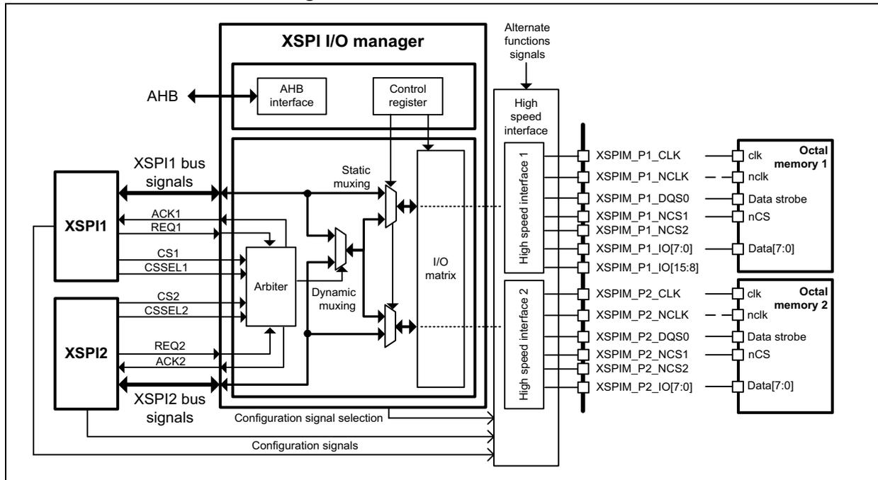
The diagram illustrates the XSPI direct octal mode architecture. On the left, two XSPI blocks, XSPI1 and XSPI2, are shown. XSPI1 connects to the XSPI I/O manager via 'XSPI1 bus signals' (ACK1, REQ1, CS1, CSSEL1). XSPI2 connects via 'XSPI2 bus signals' (REQ2, ACK2, CS2, CSSEL2). The XSPI I/O manager contains an 'AHB interface', a 'Control register', an 'Arbiter', 'Static muxing', 'Dynamic muxing', and an 'I/O matrix'. It also receives 'Configuration signal selection' and 'Configuration signals'. The manager outputs 'Alternate functions signals' to two 'High speed interface' blocks. These interfaces connect to two 'Octal memory' blocks. The connections to Octal memory 1 are: XSPIM_P1_CLK (clk), XSPIM_P1_NCLK (nclk), XSPIM_P1_DQS0 (Data strobe), XSPIM_P1_NCS1 (nCS), XSPIM_P1_NCS2, XSPIM_P1_IO[7:0] (Data[7:0]), and XSPIM_P1_IO[15:8]. The connections to Octal memory 2 are: XSPIM_P2_CLK (clk), XSPIM_P2_NCLK (nclk), XSPIM_P2_DQS0 (Data strobe), XSPIM_P2_NCS1 (nCS), XSPIM_P2_NCS2, and XSPIM_P2_IO[7:0] (Data[7:0]).
25.5.2 XSPI direct 16-bit mode
This is the baseline mode, completely similar to XSPI octal direct mode, where each XSPI directly drives the corresponding port (XSPI1 connected to Port 1, XSPI2 connected to Port 2). Two DQS (1 per byte) are needed for each 16-bit port, when available.
Figure 216. XSPI direct 16-bit mode
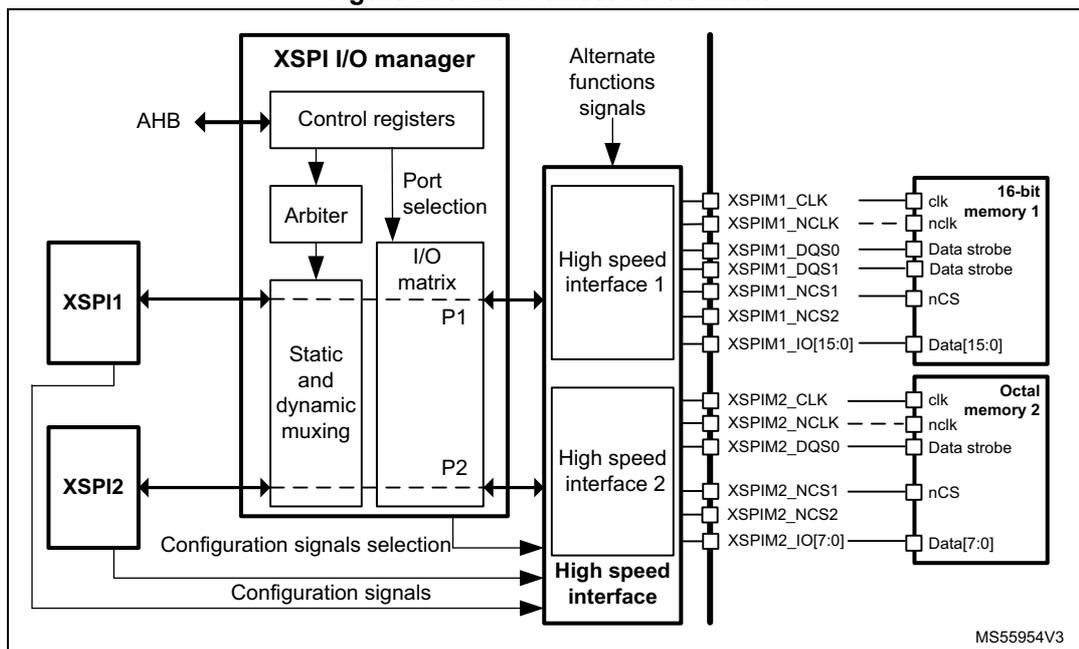
This block diagram shows the XSPI I/O manager in direct 16-bit mode. The internal architecture includes Control registers connected to an AHB bus, an Arbiter, and a Static and dynamic muxing block. The muxing block interfaces with XSPI1 and XSPI2. It connects to an I/O matrix with ports P1 and P2. Port P1 connects to High speed interface 1, and Port P2 connects to High speed interface 2. These interfaces connect to external memories via a set of signals: XSPIM1_CLK, XSPIM1_NCLK, XSPIM1_DQS0, XSPIM1_DQS1, XSPIM1_NCS1, XSPIM1_NCS2, and XSPIM1_IO[15:0] for a 16-bit memory 1; and XSPIM2_CLK, XSPIM2_NCLK, XSPIM2_DQS0, XSPIM2_NCS1, XSPIM2_NCS2, and XSPIM2_IO[7:0] for an Octal memory 2. Configuration signals are also routed to a common High speed interface block. The diagram is labeled with MS55954V3.
25.5.3 XSPI dual-octal mode
This mode is equivalent to XSPI direct mode, but, for simplicity, only one XSPI interface is represented. Two external octal memories are accessed in parallel, similarly to the dual-quad mode implemented with octal interfaces.
Figure 217. XSPI dual-octal mode
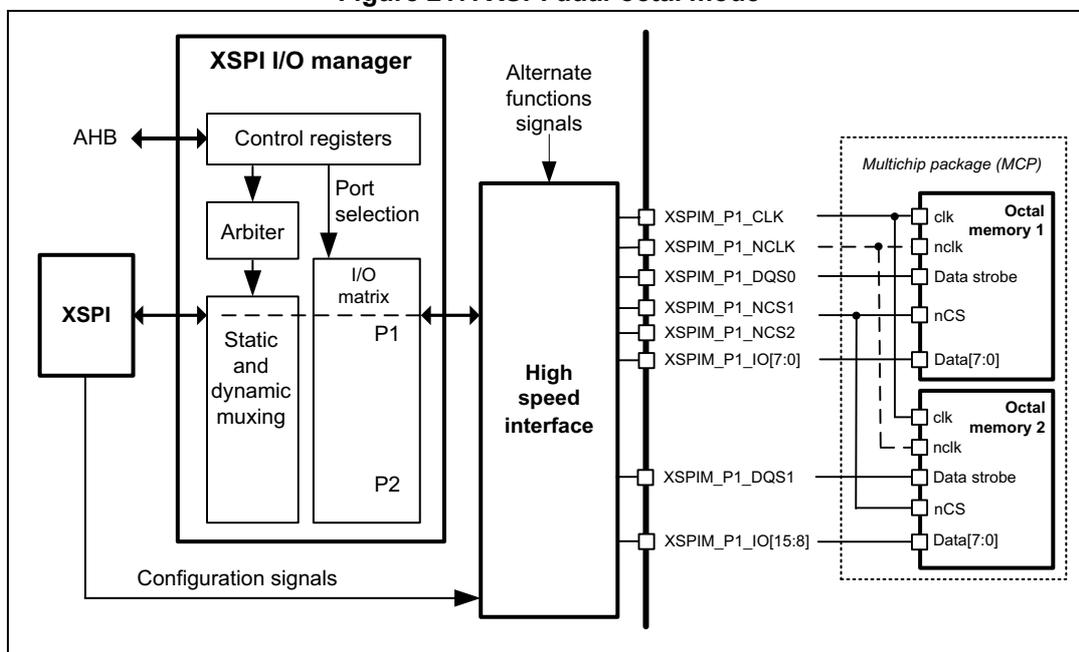
This block diagram illustrates the XSPI dual-octal mode. The XSPI I/O manager contains Control registers (AHB interface), an Arbiter, and Static and dynamic muxing connected to a single XSPI block. The I/O matrix uses ports P1 and P2, with P1 feeding into a High speed interface. The output signals include XSPIM_P1_CLK, XSPIM_P1_NCLK, XSPIM_P1_DQS0, XSPIM_P1_NCS1, XSPIM_P1_NCS2, and XSPIM_P1_IO[7:0] which connect to Octal memory 1. Additionally, XSPIM_P1_DQS1 and XSPIM_P1_IO[15:8] connect to Octal memory 2. Both memories are housed within a Multichip package (MCP). Configuration signals are routed from the muxing block to the High speed interface.
25.5.4 XSPI swapped mode
This mode is similar to XSPI direct mode, but the ports are swapped, to help I/O mapping. The mode is selected by bits XSPIM_CR[1:0].
If XSPIM.CR[0] or XSPIM.CR[1] is toggled in application, XSPI DCR2 or XSPI.CCR must be written, so that the calibration of the high speed interface is launched according to the new XSPI using it.
Note: In swapped mode, the XSPI2 can be configured in 16-bit mode, and the XSPI1 can be configured in octal mode, to connect an external 16-bit memory on Port 1, and to connect in a concurrent way an octal external memory connected to Port 2 of the I/O manager.
Figure 218. XSPI swapped (octal) mode
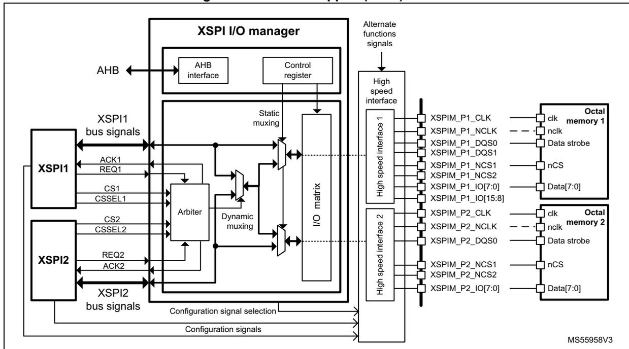
The diagram illustrates the XSPI swapped (octal) mode configuration. On the left, two XSPI controllers, XSPI1 and XSPI2, are shown. XSPI1 is connected to 'Octal memory 1' and XSPI2 is connected to 'Octal memory 2'. Both XSPIs send bus signals (ACK1, REQ1, CS1, CSSEL1, CS2, CSSEL2, REQ2, ACK2) to an 'XSPI I/O manager' block. The XSPI I/O manager contains an 'AHB interface', a 'Control register', 'Static muxing', 'Dynamic muxing', and an 'I/O matrix'. The I/O matrix connects to two 'High speed interface' blocks. These interfaces are connected to the external memories. The signals between the High speed interfaces and the memories are: XSPIM_P1_CLK, XSPIM_P1_NCLK, XSPIM_P1_DQS0, XSPIM_P1_DQS1, XSPIM_P1_NCS1, XSPIM_P1_NCS2, XSPIM_P1_IO[7:0], XSPIM_P1_IO[15:8] for Port 1; and XSPIM_P2_CLK, XSPIM_P2_NCLK, XSPIM_P2_DQS0, XSPIM_P2_NCS1, XSPIM_P2_NCS2, XSPIM_P2_IO[7:0] for Port 2. The memories are labeled 'Octal memory 1' and 'Octal memory 2' with pins for clk, nclk, Data strobe, nCS, and Data[7:0]. A 'Configuration signal selection' line connects the I/O manager to the High speed interfaces. The diagram is labeled 'MS55958V3' in the bottom right corner.
25.5.5 Two XSPIs multiplexed mode to Port 1 accessing two external memories
If only one output port is used to access two memories, alternate function signals can be routed to pins corresponding to the other port. This mode is selected by bits XSPIM_CR[1:0].
The arbiter in the IO manager selects XSPI1 or XSPI2 to own the octal-SPI bus according to the existing transfer requests and status of the two MAXTRAN fairness counters.
The external memories can be on separate chips, or embedded in a single multichip package. In this case, each memory requests a dedicated Chip select, selected according to the CSSEL control of the XSPI currently owning the bus.
The configuration signals of the high speed interface toggle when the corresponding XSPI is selected, because the timing characteristics of the two memories can be different.
Figure 219. XSPI multiplexed mode to Port 1
![Figure 219: XSPI multiplexed mode to Port 1. Block diagram showing the XSPI I/O manager connected to two XSPI interfaces (XSPI1 and XSPI2) and two external memories (Octal memory 1 and Octal memory 2) via High speed interfaces. The XSPI I/O manager includes an AHB interface, Control register, Static muxing, Dynamic muxing, and an I/O matrix. The XSPI1 and XSPI2 interfaces are connected to the I/O matrix via bus signals (ACK1, REQ1, CS1, CSSEL1, CS2, CSSEL2, REQ2, ACK2). The High speed interfaces are connected to the I/O matrix via signals (XSPIM_P1_CLK, XSPIM_P1_NCLK, XSPIM_P1_DQS0, XSPIM_P1_DQS1, XSPIM_P1_NCS1, XSPIM_P1_NCS2, XSPIM_P1_IO[7:0], XSPIM_P1_IO[15:8] for Port 1 and XSPIM_P2_CLK, XSPIM_P2_NCLK, XSPIM_P2_DQS0, XSPIM_P2_NCS1, XSPIM_P2_NCS2, XSPIM_P2_IO[7:0] for Port 2). The Octal memory 1 and Octal memory 2 are connected to the High speed interfaces via signals (clk, nclk, Data strobe, nCS, Data[7:0]).](/RM0477-STM32H7Rx-7Sx/aac495a79112c3be5cc72756fd84db5f_img.jpg)
Figure 219 illustrates the XSPI multiplexed mode to Port 1. The XSPI I/O manager is connected to an AHB interface and a Control register. It contains an Arbiter, Static muxing, Dynamic muxing, and an I/O matrix. Two XSPI interfaces, XSPI1 and XSPI2, are connected to the I/O matrix via bus signals (ACK1, REQ1, CS1, CSSEL1, CS2, CSSEL2, REQ2, ACK2). The I/O matrix is connected to two High speed interfaces (High speed interface 1 and High speed interface 2) via signals (XSPIM_P1_CLK, XSPIM_P1_NCLK, XSPIM_P1_DQS0, XSPIM_P1_DQS1, XSPIM_P1_NCS1, XSPIM_P1_NCS2, XSPIM_P1_IO[7:0], XSPIM_P1_IO[15:8] for Port 1 and XSPIM_P2_CLK, XSPIM_P2_NCLK, XSPIM_P2_DQS0, XSPIM_P2_NCS1, XSPIM_P2_NCS2, XSPIM_P2_IO[7:0] for Port 2). The High speed interfaces are connected to two Octal memories (Octal memory 1 and Octal memory 2) via signals (clk, nclk, Data strobe, nCS, Data[7:0]).
25.5.6 Two XSPIs multiplexed mode to Port 2 accessing two external memories
This is similar to XSPI multiplexed mode to Port 1, but the target is Port 2. This mode is selected by bits XSPIM_CR[2:1].
Figure 220. XSPI multiplexed (octal and dual-octal) mode to Port 2
![Figure 220: XSPI multiplexed (octal and dual-octal) mode to Port 2. Block diagram showing the XSPI I/O manager connected to two XSPI interfaces (XSPI1 and XSPI2) and two external memories (Octal memory 1 and Octal memory 2) via High speed interfaces. The XSPI I/O manager includes an AHB interface, Control register, Static muxing, Dynamic muxing, and an I/O matrix. The XSPI1 and XSPI2 interfaces are connected to the I/O matrix via bus signals (ACK1, REQ1, CS1, CSSEL1, CS2, CSSEL2, REQ2, ACK2). The I/O matrix is connected to two High speed interfaces (High speed interface 1 and High speed interface 2) via signals (XSPIM_P1_CLK, XSPIM_P1_NCLK, XSPIM_P1_DQS0, XSPIM_P1_DQS1, XSPIM_P1_NCS1, XSPIM_P1_NCS2, XSPIM_P1_IO[15:0] for Port 1 and XSPIM_P2_CLK, XSPIM_P2_NCLK, XSPIM_P2_DQS0, XSPIM_P2_NCS1, XSPIM_P2_NCS2, XSPIM_P2_IO[7:0] for Port 2). The High speed interfaces are connected to two Octal memories (Octal memory 1 and Octal memory 2) via signals (clk, nclk, Data strobe, nCS, Data[7:0]).](/RM0477-STM32H7Rx-7Sx/b798cebca347e12dd703a57926eb5a11_img.jpg)
Figure 220 illustrates the XSPI multiplexed (octal and dual-octal) mode to Port 2. The XSPI I/O manager is connected to an AHB interface and a Control register. It contains an Arbiter, Static muxing, Dynamic muxing, and an I/O matrix. Two XSPI interfaces, XSPI1 and XSPI2, are connected to the I/O matrix via bus signals (ACK1, REQ1, CS1, CSSEL1, CS2, CSSEL2, REQ2, ACK2). The I/O matrix is connected to two High speed interfaces (High speed interface 1 and High speed interface 2) via signals (XSPIM_P1_CLK, XSPIM_P1_NCLK, XSPIM_P1_DQS0, XSPIM_P1_DQS1, XSPIM_P1_NCS1, XSPIM_P1_NCS2, XSPIM_P1_IO[15:0] for Port 1 and XSPIM_P2_CLK, XSPIM_P2_NCLK, XSPIM_P2_DQS0, XSPIM_P2_NCS1, XSPIM_P2_NCS2, XSPIM_P2_IO[7:0] for Port 2). The High speed interfaces are connected to two Octal memories (Octal memory 1 and Octal memory 2) via signals (clk, nclk, Data strobe, nCS, Data[7:0]).
Note: It is possible to connect a 16-bit memory on Port 1, whereas Port 2 uses multiplexing mode on two octal memories.
25.5.7 XSPI1 and XSPI2 drive a single external memory
This is similar to XSPIs multiplexed mode to Port 1, but in this case only one external memory is present. Both CSSEL controls must target the same NCS (NCS1 in Figure 221).
Figure 221. XSPI1 and XSPI2 drive a single external memory (octal mode)
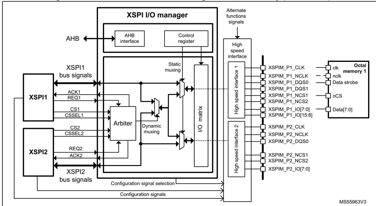
The diagram illustrates the internal architecture of the XSPI I/O manager and its connection to external memory. On the left, two XSPI controllers, XSPI1 and XSPI2, are shown. XSPI1 connects to the manager via bus signals including ACK1, REQ1, CS1, and CSSEL1. XSPI2 connects via CS2, CSSEL2, REQ2, and ACK2. Both controllers also receive configuration signals. The XSPI I/O manager contains an AHB interface connected to an AHB bus, a Control register, an Arbiter, Static muxing, Dynamic muxing, and an I/O matrix. The Arbiter receives inputs from both XSPI controllers and manages access through the muxing stages to the I/O matrix. The I/O matrix outputs are connected to two High speed interfaces. High speed interface 1 connects to Octal memory 1 with signals: XSPIM_P1_CLK (clk), XSPIM_P1_NCLK (nclk), XSPIM_P1_DQS0 (Data strobe), XSPIM_P1_DQS1, XSPIM_P1_NCS1 (nCS), XSPIM_P1_NCS2, XSPIM_P1_IO[7:0] (Data[7:0]), and XSPIM_P1_IO[15:8]. High speed interface 2 provides alternate function signals: XSPIM_P2_CLK, XSPIM_P2_NCLK, XSPIM_P2_DQS0, XSPIM_P2_NCS1, XSPIM_P2_NCS2, and XSPIM_P2_IO[7:0]. A label 'MS55963V3' is present in the bottom right corner.
This use case is valid even when Port 2 is used instead of Port 1, and also possible with XSPI1 and XSPI2 interfacing a 16-bit memory (connecting XSPIM_P1_DQS1 to the memory).
25.5.8 A single XSPI drives two external memories
This is a subset of direct mode and corresponds to semi-dynamic switching. There are two target memories, but the arbiter is not used. The software must set the XSPI1 chip selector (bit 24 of the XSPI_CR register) each time the target memory changes.
The baseline use case boots on flash (memory1) and then switches to SRAM (memory2) for the rest of the application.
Figure 222. Single XSPI driving two external memories
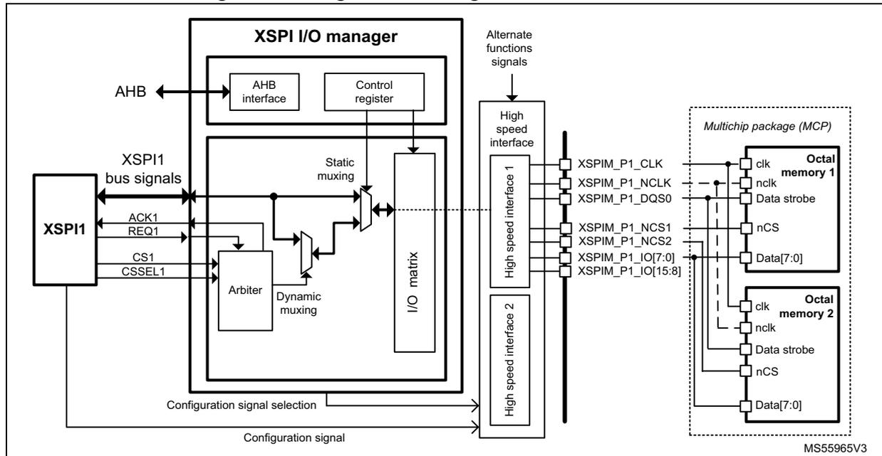
The diagram illustrates the internal architecture of the XSPI I/O manager and its connection to two external memories. On the left, an XSPI1 block is connected to the XSPI I/O manager via XSPI1 bus signals (ACK1, REQ1, CS1, CSSEL1). The XSPI I/O manager contains an AHB interface connected to an AHB bus, a Control register , an Arbiter , Static muxing , Dynamic muxing , and an I/O matrix . The Arbiter receives configuration signals and controls the Static muxing and Dynamic muxing blocks. The Static muxing block connects to the I/O matrix . The I/O matrix is connected to two High speed interface blocks, labeled High speed interface 1 and High speed interface 2 . These interfaces are connected to a Multipack package (MCP) containing two Octal memory blocks, Octal memory 1 and Octal memory 2 . The connections between the interfaces and the memories are: XSPIM_P1_CLK to clk , XSPIM_P1_NCLK to nclk , XSPIM_P1_DQS0 to Data strobe , XSPIM_P1_NCS1 to nCS for memory 1, XSPIM_P1_NCS2 to nCS for memory 2, XSPIM_P1_IO[7:0] to Data[7:0] for memory 1, and XSPIM_P1_IO[15:8] to Data[7:0] for memory 2. The XSPI I/O manager also receives Alternate functions signals and a Configuration signal (via Configuration signal selection ).
This use case shows a configuration using XSPI1 on Port 1. It is also valid if the instance is XSPI2 instead of XSPI1, but with MODE = 1. The use case is also valid when Port 2 is used instead of Port 1, by configuring MODE bit according to the instance (XSPI1 or XSPI2) driving the two external memories.
25.6 XSPIM registers
25.6.1 XSPIM control register (XSPIM_CR)
Address offset: 0x0000
Reset value: 0x0000 0000
| 31 | 30 | 29 | 28 | 27 | 26 | 25 | 24 | 23 | 22 | 21 | 20 | 19 | 18 | 17 | 16 |
|---|---|---|---|---|---|---|---|---|---|---|---|---|---|---|---|
| Res. | Res. | Res. | Res. | Res. | Res. | Res. | Res. | REQ2ACK_TIME[7:0] | |||||||
| rw | rw | rw | rw | rw | rw | rw | rw | ||||||||
| 15 | 14 | 13 | 12 | 11 | 10 | 9 | 8 | 7 | 6 | 5 | 4 | 3 | 2 | 1 | 0 |
| Res. | Res. | Res. | Res. | Res. | Res. | Res. | Res. | Res. | CSSEL_OVR_O2 | CSSEL_OVR_O1 | CSSEL_OVR_EN | Res. | Res. | MODE | MUXEN |
| rw | rw | rw | rw | rw | |||||||||||
Bits 31:24 Reserved, must be kept at reset value.
Bits 23:16 REQ2ACK_TIME[7:0] : REQ to ACK time
In Multiplexed mode (MUXEN = 1), this field defines the time between two transactions.
The value is the number of XSPI clock cycles - 1
Bits 15:7 Reserved, must be kept at reset value.
Bit 6 CSSEL_OVR_O2 : Chip select selector override setting for XSPI2
0: the chip select signal from XSPI2 is sent to NCS1
1: the chip select signal from XSPI2 is sent to NCS2
Bit 5 CSSEL_OVR_O1 : Chip select selector override setting for XSPI1
0: the chip select signal from XSPI1 is sent to NCS1
1: the chip select signal from XSPI1 is sent to NCS2
Bit 4 CSSEL_OVR_EN : Chip select selector override enable
0: override not enabled
1: CSSEL_OVR_O1 and CSSEL_OVR_O2 bit values overwrite the CSSEL signal values coming from XSPI1 and XSPI2
Bits 3:2 Reserved, must be kept at reset value.
Bit 1 MODE : XSPI multiplexing mode
0: if MUXEN = 0 direct mode, if MUXEN = 1 arbitration mode to output Port 1
1: if MUXEN = 0 swapped mode, if MUXEN = 1 arbitration mode to output Port 2
Bit 0 MUXEN : Multiplexed mode enable
This bit enables the multiplexing of the two XSPIs.
0: No multiplexing, hence no arbitration
1: XSPI1 and XSPI2 are multiplexed over the same bus
25.6.2 XSPIM register map
Table 219. XSPIM register map and reset values
| Offset | Register name | 31 | 30 | 29 | 28 | 27 | 26 | 25 | 24 | 23 | 22 | 21 | 20 | 19 | 18 | 17 | 16 | 15 | 14 | 13 | 12 | 11 | 10 | 9 | 8 | 7 | 6 | 5 | 4 | 3 | 2 | 1 | 0 |
|---|---|---|---|---|---|---|---|---|---|---|---|---|---|---|---|---|---|---|---|---|---|---|---|---|---|---|---|---|---|---|---|---|---|
| 0x0000 | XSPIM_CR | Res. | Res. | Res. | Res. | Res. | Res. | Res. | Res. | REQ2ACK_TIME[7:0] | Res. | Res. | Res. | Res. | Res. | Res. | Res. | Res. | Res. | 0 | 0 | 0 | Res. | Res. | MODE | MUXEN | |||||||
| Reset value | 0 | 0 | 0 | 0 | 0 | 0 | 0 | 0 | 0 | 0 | |||||||||||||||||||||||
Refer to Section 2.3: Memory organization for the register boundary addresses.