24. Extended-SPI interface (XSPI)
24.1 XSPI introduction
The XSPI supports most external serial memories such as serial PSRAMs, serial NAND and serial NOR flash memories, HyperRAM™ and HyperFlash™ memories, with the following functional modes:
- • indirect mode: all the operations are performed using the XSPI registers to preset commands, addresses, data, and transfer parameters.
- • automatic status-polling mode: the external memory status register is periodically read and an interrupt can be generated in case of flag setting. This feature is only available in regular-command protocol.
- • memory-mapped mode: the external memory is memory mapped and it is seen by the system as if it was an internal memory, supporting both read and write operations.
The XSPI supports the following protocols with associated frame formats:
- • the regular-command frame format with the command, address, alternate byte, dummy cycles, and data phase
- • the HyperBus™ frame format
24.2 XSPI main features
- • Functional modes: indirect, automatic status-polling, and memory-mapped
- • Read and write support in memory-mapped mode
- • Support for single, dual, quad, and octal communication
- • Dual-memory configuration, where 8 bits can be sent/received simultaneously by accessing two quad or two octal memories in parallel
- • XSPI mode accessing a single 16-bit memory
- • SDR (single-data rate) and DTR (double-transfer rate) support
- • Data strobe support
- • Fully programmable opcode
- • Fully programmable frame format
- • Support wrapped-type access to memory in read direction
- • HyperBus support
- • Integrated FIFO for reception and transmission
- • 8-, 16-, and 32-bit data accesses allowed
- • DMA protocol support
- • DMA channel for indirect mode operations
- • Interrupt generation on FIFO threshold, timeout, operation complete, and access error
- • AXI interface with transaction acceptance limited to one: the interface accepts the next transfer on AXI bus only once the previous is completed on memory side.
- • Dual chip select support (NCS1 and NCS2)
24.3 XSPI implementation
Table 208. XSPI implementation
| Feature | XSPI1/2 |
|---|---|
| HyperBus standard compliant | X |
| Xccela standard compliant | X |
| XSPI (JESD251C) standard compliant | X |
| AMBA® AXI compliant data interface | X |
| Asynchronous AXI clock versus kernel clock | X |
| Functional modes: indirect, automatic status-polling, and memory-mapped | X |
| Dual chip select support (NCS1 and NCS2) | X |
| Read and write support in memory-mapped mode | X |
| Dual-quad configuration | X |
| Dual-octal configuration | X |
| SDR (single-data rate) and DTR (double-transfer rate) | X |
| Data strobe (DS, DQS) | X |
| Fully programmable opcode | X |
| Fully programmable frame format | X |
| Integrated FIFO for reception and transmission | X |
| 8, 16, and 32-bit data accesses | X |
| Interrupt on FIFO threshold, timeout, operation complete, and access error | X |
| Compliant with dual-XSPI arbiter (communication regulation) | X |
| Extended CSHT timeout | X |
| Memory-mapped write | X |
| Refresh counter | X |
| High-speed interface | X |
| GP/HPDMA interface | X |
| Prefetch disable | - |
| Prefetch hardware software | - |
24.4 XSPI functional description
24.4.1 XSPI block diagram
The block diagrams provided below correspond to a single XSPI connected to the I/O ports. In case several XSPIs are connected to the I/O ports through the XSPIM I/O manager, refer to Section 25: XSPI I/O manager (XSPIM) for more details.
Figure 191. XSPI block diagram for 16-bit configuration (1)
The diagram illustrates the internal architecture of the XSPI interface within an STM32 microcontroller and its connection to an external 16-bit SPI memory. The internal components include an AHB interface, AXI interface, xspi_ker_ck and xspi_nrst pins, DMA signals, and 6 interrupts. The core logic consists of Registers/control, Clock management, RX/TX data FIFO, and a Shift register. These are connected to the XSPIM port1 High-speed interface, which is linked to the STM32 via signals from the ALT function. The interface pins are: XSPIM_P1_NCLK, XSPIM_P1_CLK, XSPIM_P1_IO0 through XSPIM_P1_IO15, XSPIM_P1_DQS0, XSPIM_P1_DQS1, XSPIM_P1_NCS1, and XSPIM_P1_NCS2 (1) . The external 16-bit SPI memory pins are: NCLK, CLK, IO0 through IO15, (RW)DS0, (RW)DS1, and NCS. The XSPIM_P1_NCS2 (1) pin is connected to another memory or the second NCS of the MCP. A legend indicates that dashed lines represent signals connected or not depending on the board configuration. A note states that the configuration with NCS2 used corresponds to a semi-static management with two external memories hooked on the same XSPI bus, where software selects which memory is accessed. The document code MSV66951V3 is shown in the bottom right.
--- Signal connected or not depending on the board configuration
(1) The configuration with NCS2 used corresponds to a semi-static management with two external memories hooked on the same XSPI bus. The software selects which memory is accessed.
MSV66951V3
- 1. The configuration depends on the package (see the datasheet for more details).
Figure 192. XSPI block diagram for dual-octal configuration (1)
STM32
Signals from ALT function
Octo-SPI memory 1
Octo-SPI memory 2
Registers/control
Clock management
RX/TX data FIFO
Shift register
XSPIM port1
High-speed interface
AHB
AXI
xspi_ker_ck
xspi_nrst
DMA signals
Interrupts 6
XSPI
XSPI_CSSEL
XSPI_CS
XSPIM_P1_NCLK
XSPIM_P1_CLK
XSPIM_P1_IO0
XSPIM_P1_IO1
XSPIM_P1_IO2
XSPIM_P1_IO3
XSPIM_P1_IO4
XSPIM_P1_IO5
XSPIM_P1_IO6
XSPIM_P1_IO7
XSPIM_P1_DQS0
XSPIM_P1_IO8
XSPIM_P1_IO9
XSPIM_P1_IO10
XSPIM_P1_IO11
XSPIM_P1_IO12
XSPIM_P1_IO13
XSPIM_P1_IO14
XSPIM_P1_IO15
XSPIM_P1_DQS1
XSPIM_P1_NCS1
XSPIM_P1_NCS2 (1)
To another memory or second NCS of MCP
----- Signal connected or not depending on the board configuration
(1) The configuration with NCS2 used corresponds to a semi-static management with two external memories hooked on the same XSPI bus. The software selects which memory is accessed.
MSv66952V3
- 1. The configuration depends on the package (see the datasheet for more details).
Figure 193. XSPI block diagram for octal configuration
The diagram illustrates the internal architecture of the XSPI peripheral within an STM32 microcontroller and its connection to an external Octo-SPI memory. The internal components include an AHB interface, AXI interface, RX/TX data FIFO, Shift register, Registers/control, and Clock management. The XSPI peripheral is connected to the STM32 via a High-speed interface (XSPIM port1). The memory is connected to the XSPIM_P1 pins of the STM32. The connections are as follows:
- XSPIM_P1_NCLK (dashed line) connects to NCLK
- XSPIM_P1_CLK connects to CLK
- XSPIM_P1_IO0 through XSPIM_P1_IO7 connect to IO0 through IO7
- XSPIM_P1_IO8 through XSPIM_P1_IO15 are not connected to the memory
- XSPIM_P1_DQS0 connects to (RW)DS0
- XSPIM_P1_DQS1 is not connected
- XSPIM_P1_NCS1 connects to NCS
- XSPIM_P1_NCS2 (dashed line) connects to another memory or second NCS of MCP
Other signals shown include:
- AHB, AXI, RX/TX data FIFO, Shift register, Registers/control, and Clock management are internal to the XSPI block.
- xspi_ker_ck and xspi_nrst are input signals to the XSPI block.
- DMA signals and Interrupts (6) are input signals to the XSPI block.
- Signals from ALT function are input to the High-speed interface.
- XSPI_CSSEL and XSPI_CS are output signals from the Shift register to the High-speed interface.
Legend:
- ----- Signal connected or not depending on the board configuration
Notes:
- (1) The Octo-SPI memory is connected to XSPIM_P1_IO[0:7] but it can also be connected to XSPIM_P1_IO[8:15].
- (2) The configuration with NCS2 used corresponds to a semi-static management with two external memories hooked on the same XSPI bus. The software selects which memory is accessed.
MSV66953V4
Figure 194. XSPI block diagram in quad configuration
The diagram illustrates the internal architecture of the XSPI interface within an STM32 microcontroller. On the left, the XSPI block contains several functional units: 'Registers/control' connected to the AHB bus; 'Clock management' receiving 'xspi_ker_ck' and 'xspi_nrst' signals; 'RX/TX data FIFO' connected to the AXI bus; and a 'Shift register'. These units are interconnected and also connect to the 'High-speed interface' (XSPIM port1). Control signals 'XSPI_CSSEL' and 'XSPI_CS' are also shown. The 'High-speed interface' connects to the STM32 core and provides 'Signals from ALT function'. The interface pins are labeled as follows: XSPIM_P1_NCLK, XSPIM_P1_CLK, XSPIM_P1_IO0 through XSPIM_P1_IO15, XSPIM_P1_DQS0, XSPIM_P1_DQS1, XSPIM_P1_NCS1, and XSPIM_P1_NCS2. The pins are connected to an external 'Quad-SPI memory' as follows: XSPIM_P1_CLK to CLK, XSPIM_P1_IO0 to IO0, XSPIM_P1_IO1 to IO1, XSPIM_P1_IO2 to IO2, XSPIM_P1_IO3 to IO3, and XSPIM_P1_NCS1 to NCS. XSPIM_P1_NCS2 is connected to 'another memory or second NCS of MCP'. At the bottom, two footnotes explain the memory connection options and the semi-static management configuration. The reference code MSV66954V4 is also present.
(1) The Quad-SPI memory is connected to XSPIM_P1_IO[0:3] but it can also be connected to XSPIM_P1_IO[4:7], XSPIM_P1_IO[8:11], or XSPIM_P1_IO[12:15].
(2) The configuration with NCS2 used corresponds to a semi-static management with two external memories hooked on the same XSPI bus. The software selects which memory is accessed.
MSV66954V4
Figure 195. XSPI block diagram for dual-quad configuration
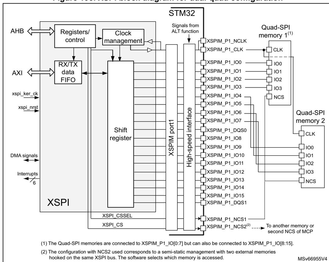
The diagram shows the internal architecture of the XSPI interface within an STM32 microcontroller. The interface connects to the AHB bus for registers/control and the AXI bus for RX/TX data FIFO. A clock management block receives xspi_ker_ck and signals from ALT functions, providing clocks to the shift register and output pins. The shift register handles data transfer between the FIFO and the XSPIM port 1 high-speed interface. External signals include xspi_nrst, DMA signals, and 6 interrupts. The high-speed interface connects to two Quad-SPI memories. Quad-SPI memory 1 is connected to XSPIM_P1_CLK, XSPIM_P1_IO0-IO3, and XSPIM_P1_NCS. Quad-SPI memory 2 is connected to XSPIM_P1_CLK, XSPIM_P1_IO8-IO11, and XSPIM_P1_NCS. Additional pins like XSPIM_P1_NCLK, DQS0, DQS1, and IO4-IO7, IO12-IO15 are also shown. Footnotes explain memory connection flexibility and NCS2 usage for semi-static management.
(1) The Quad-SPI memories are connected to XSPIM_P1_IO[0:7] but can also be connected to XSPIM_P1_IO[8:15].
(2) The configuration with NCS2 used corresponds to a semi-static management with two external memories hooked on the same XSPI bus. The software selects which memory is accessed.
MSv66955V4
24.4.2 XSPI pins and internal signals
Table 209. XSPI input/output pins (1)
| Pin name | Type | Description |
|---|---|---|
| XSPIM_Px_NCLK | Output | XSPI inverted clock to support 1.8 V HyperBus protocol. |
| XSPIM_Px_CLK | Output | XSPI clock |
| XSPIM_Px_IOn (n = 0 to 15) | Input/output | XSPI data pins |
| XSPIM_Px_NCS1,2 | Output | Chip select for the memory |
| XSPIM_Px_DQS0,1 | Input/output | Data strobe/write mask signal from/to the memory |
1. x = 1 to 2.
Caution: Use the same configuration (output speed, HSLV) for all XSPI input/output pins to avoid any data corruption.
Table 210. XSPI internal signals
| Signal name | Type | Description |
|---|---|---|
| xspi_hclk | Input | XSPI AHB clock |
| xspi_aclk | Input | XSPI AXI clock |
Table 210. XSPI internal signals
| Signal name | Type | Description |
|---|---|---|
| xspi_ker_ck | Input | XSPI kernel clock |
| xspi_dma | N/A | DMA request signal |
| xspi_it | Output | Global interrupt line (see Table 214 for the multiple sources of interrupt) |
24.4.3 Clock constraints
The XSPI AXI clock (xspi_aclk) has to be greater or equal than the XSPI kernel clock (xspi_ker_ck).
24.4.4 XSPI interface to memory modes
The XSPI supports the following protocols:
- • regular-command protocol
- • HyperBus protocol
The XSPI uses from 6 to 21 signals to interface with a memory, depending on the functional mode:
- • NCS: chip-select (in the following sections, unless otherwise specified, NCS applies for NCS1 or NCS2. Only one of these two signals is active at a given moment in time).
- • CLK: communication clock
- • NCLK: inverted clock used only in the 1.8 V HyperBus protocol
- • DQS0, DQS1: data strobe used only in regular-command protocol
- • IO[3:0]: data bus LSB
- • IO[7:4]:
- – data bus MSB used in dual-quad and octal configurations
- – data bus used as possible remap for quad-SPI mode
- • IO[15:8]:
- – data bus MSB used in dual-quad, dual-octal and 16-bit configurations
- – data bus used as possible remap for octal-SPI mode
- – IO[15:12] and IO[11:8] can also be used as possible remap for quad-SPI mode
24.4.5 XSPI regular-command protocol
When in regular-command protocol, the XSPI communicates with the external device using commands. Each command can include the following phases:
- • instruction phase
- • address phase
- • alternate-byte phase
- • dummy-cycle phase
- • data phase
Only the data phase uses 16 bits. Instruction, address, and alternate phases use only the eight LSB of the bus as for octal configuration.
Any of these phases can be configured to be skipped, but single-phase commands supported are only those with instruction phase.
The NCS falls before the start of each command and rises again after each command finishes.
In memory-mapped mode, both read and write operation are supported: as a consequence, some of the configuration registers are duplicated to specify write operations (read operations are configured using regular registers).
Figure 196. SDR read command in 16-bit configuration
![Timing diagram for SDR read command in 16-bit configuration. The diagram shows the relationship between NCS (Active Low Chip Select), CLK (Clock), and IO[7:0] (I/O lines). NCS is shown as a signal that goes low before the command starts and returns high after the command finishes. CLK is a periodic square wave. IO[7:0] is shown as a sequence of data elements: a shaded 'Ech' (Instruction phase), '13h' (Address phase), a group of four elements labeled 'A[31:24]', 'A[23:16]', 'A[15:8]', and 'A[7:0]' (collectively labeled 'Address'), a shaded 'Dummy' phase, and four data elements 'D0', 'D1', 'D2', and 'D3' (labeled 'Pre-drive'). The diagram is labeled 'MSV43488V1' in the bottom right corner.](/RM0477-STM32H7Rx-7Sx/4e2787869041c4ecde7663f294af050f_img.jpg)
- 1. Data (such as D0, D1, D2) are sent in 16-bit configuration mode over IO[15:0]. Only the command and address are sent over IO[7:0] as for octal mode.
The specific regular-command protocol features are configured through the registers in the 0x0100-0x01FC offset range.
Instruction phase
During this phase, a 1- to 4-byte instruction is sent to the external device specifying the type of operation to be performed. The size of the instruction to be sent is configured in ISIZE[1:0] of XSPI_CCR and the instruction is programmed in INSTRUCTION[31:0] of XSPI_IR.
The instruction phase can optionally send:
- • 1 bit at a time (over IO0, SO signal in single-SPI mode)
- • 2 bits at a time (over IO0/IO1 in dual-SPI mode)
- • 4 bits at a time (over IO0 to IO3 in quad-SPI mode)
- • 8 bits at a time (over IO0 to IO7 in octal-SPI mode, or in 16-bit SPI mode)
This can be configured using IMODE[2:0] of XSPI_CCR.
The instruction can be sent in DTR (double-transfer rate) mode on each rising and falling edge of the clock, by setting IDTR in XSPI_CCR.
When IMODE[2:0] = 000 in XSPI_CCR, the instruction phase is skipped, and the command sequence starts with the address phase, if present.
When in memory-mapped mode, the instruction used for the write operation is specified in XSPI_WIR and the instruction format is specified in XSPI_WCCR. The instruction used for the read operation and the instruction format are specified in XSPI_IR and XSPI_CCR.
Address phase
In the address phase, 1 to 4 bytes are sent to the external device, to indicate the address of the operation. The number of address bytes to be sent is configured in ADSIZE[1:0] of XSPI_CCR.
In indirect and automatic status-polling modes, the address bytes to be sent are specified in ADDRESS[31:0] of XSPI_AR. In memory-mapped mode, the address is given directly via the AXI (from any master in the system).
The address phase can send:
- • 1 bit at a time (over IO0, SO signal in single-SPI mode)
- • 2 bits at a time (over IO0/IO1 in dual-SPI mode)
- • 4 bits at a time (over IO0 to IO3 in quad-SPI mode)
- • 8 bits at a time (over IO0 to IO7 in octal-SPI mode, or in 16-bit SPI mode)
This can be configured using ADMODE[2:0] of XSPI_CCR.
The address can be sent in DTR mode (on each rising and falling edge of the clock) setting ADDTR in XSPI_CCR.
When ADMODE[2:0] = 000, the address phase is skipped and the command sequence proceeds directly to the next phase, if any.
In memory-mapped mode, the address format for the write operation is specified in XSPI_WCCR. The address format for the read operation is specified in XSPI_CCR.
Warning: Some memory specifications consider that each address corresponds to a 16-bit value. XSPI considers that each address corresponds to an 8-bit value. So the software needs to multiply the address by two when accessing the memory registers.
Alternate-byte phase
In the alternate-bytes phase, 1 to 4 bytes are sent to the external device, generally to control the mode of operation. The number of alternate bytes to be sent is configured in ABSIZE[1:0] of XSPI_CCR. The bytes to be sent are specified in XSPI_ABR.
The alternate-byte phase can send:
- • 1 bit at a time (over IO0, SO signal in single-SPI mode)
- • 2 bits at a time (over IO0/IO1 in dual-SPI mode)
- • 4 bits at a time (over IO0 to IO3 in quad-SPI mode)
- • 8 bits at a time (over IO0 to IO7 in octal-SPI mode, or in 16-bit SPI mode)
This can be configured using ABMODE[2:0] of XSPI_CCR.
The alternate bytes can be sent in DTR mode (on each rising and falling edge of the clock) setting ABDTR of XSPI_CCR.
When ABMODE[2:0] = 000, the alternate-bytes phase is skipped and the command sequence proceeds directly to the next phase, if any.
Only a single nibble may need to be sent during the alternate-byte phase rather than a full byte, such as when the dual-SPI mode is used and only two cycles are used for the alternate bytes.
In this case, the firmware can use the quad-SPI mode (ABMODE[2:0] = 011), and send a byte with bits 7 and 3 of ALTERNATE[31:0] set to 1 (keeping the IO3 line high), and bits 6 and 2 set to 0 (keeping the IO2 line low), in XSPI_IR.
The upper two bits of the nibble to be sent are then placed in bits 5:4 of ALTERNATE[31:0], while the lower two bits are placed in bits 1:0. For example, if the nibble 2 (0010) is to be sent over IO0/IO1, then ALTERNATE[31:0] must be set to 0x8A (1000_1010).
In memory-mapped mode, the alternate bytes used for the write operation are specified in XSPI_WABR, and the alternate byte format is specified in XSPI_WCCR. The alternate bytes used for read operation and the alternate byte format are specified in XSPI_ABR and XSPI_CCR.
Dummy-cycle phase (memory latency)
In the dummy-cycle phase, 1 to 31 cycles are given without any data being sent or received, in order to give the external device, the time to prepare for the data phase when higher clock frequencies are used. The number of cycles given during this phase is specified in DCYC[4:0] of XSPI_TCR. In both SDR and DTR modes, the duration is specified as a number of full CLK cycles.
When DCYC[4:0] = 00000, the dummy-cycle phase is skipped, and the command sequence proceeds directly to the data phase, if present.
In order to assure enough “turn-around” time for changing the data signals from the output mode to the input mode, there must be at least one dummy cycle when using the dual-, quad-, octal-, or 16-bit SPI mode, to receive data from the external device.
In memory-mapped mode, the dummy cycles for the write operations are specified in XSPI_WTCR. The dummy cycles for the read operation are specified in XSPI_TCR.
Data phase
During the data phase, any number of bytes can be sent to or received from the external device.
In indirect mode, the number of bytes to be sent/received is specified in XSPI_DLR. In this mode, the data to be sent to the external device must be written to XSPI_DR. In indirect-read mode, the data received from the external device is obtained by reading XSPI_DR.
In automatic status-polling mode, the number of bytes to be received is specified in XSPI_DLR, and the data received from the external device can be obtained by reading XSPI_DR.
In memory-mapped mode, the data read or written, is sent or received directly over the AXI to the Cortex core or to a DMA.
The data phase can send/receive:
- • 1 bit at a time (over IO0/IO1 (SO/SI respectively) in single-SPI mode)
- • 2 bits at a time (over IO0/IO1 in dual-SPI mode)
- • 4 bits at a time (over IO0 to IO3 in quad-SPI mode)
- • 8 bits at a time (over IO0 to IO7 in octal-SPI mode)
- • 16 bits at a time (over IO0 to IO15 in 16-bit SPI mode)
This can be configured using DMODE[2:0] of XSPI_CCR.
The data can be sent or received in DTR mode (on each rising and falling edge of the clock) setting DDTR of XSPI_CCR.
When DMODE[2:0] = 000, the data phase is skipped, and the command sequence finishes immediately by raising the NCS. This configuration must be used only in indirect-write mode.
In memory-mapped mode, the data format for the write operation is specified in XSPI_WCCR. The data format for the read operation is specified in XSPI_CCR.
DQS use
The DQS signal can be used for data strobing during the read transactions when the device toggles the DQS aligned with the data.
The DQS management can be enabled by setting DQSE of XSPI_CCR.
Figure 197. DTR read in octal-SPI mode with DQS (Macronix mode) example
![Timing diagram for DTR read in octal-SPI mode with DQS (Macronix mode) example. The diagram shows four signals: NCS (active low), CLK (square wave), DQS (data strobe), and IO[7:0] (data bus). The sequence starts with NCS going low, followed by CLK. The IO[7:0] bus shows a series of data packets: EEh, 11h, A[31:24], A[23:16], A[15:8], A[7:0], which are grouped as 'Address'. This is followed by a 'Dummy' phase (shaded area). Then, the DQS signal toggles, and the IO[7:0] bus shows data packets D1, D0, D3, D2, which are grouped as 'Word unit'. The diagram is labeled MSv43489V1.](/RM0477-STM32H7Rx-7Sx/a230458502e5f308b9d362340c2bbf8d_img.jpg)
24.4.6 XSPI regular-command protocol signal interface
Single-SPI mode
The legacy SPI mode allows just a single bit to be sent/received serially. In this mode, the data is sent to the external device over the SO signal (Single-SPI Output) (whose I/Os are shared with IO0). The data received from the external device arrives via SI (Single-SPI Input) (whose I/Os are shared with IO1).
Compared to the SPI legacy mode, IO0/SO and IO1/SI are respectively equivalent to MOSI and MISO, having the XSPI generating the clock.
The different phases can each be configured separately to use this single-bit mode by setting to 001 the IMODE, ADMODE, ABMODE, and DMODE fields in XSPI_CCR and XSPI_WCCR.
In each phase configured in single-SPI mode:
- • IO0 (SO) is in output mode.
- • IO1 (SI) is in input mode (high impedance).
- • IO2 is in output mode and forced to 0.
- • IO3 is in output mode and forced to 1 (to deactivate the “hold” function).
- • IO4 to IO15 are in output mode and forced to 0.
This is the case even for the dummy phase if DMODE[2:0] = 001.
Dual-SPI mode
In dual-SPI mode, two bits are sent/received simultaneously over the IO0/IO1 signals.
The different phases can each be configured separately to use dual-SPI mode by setting to 010 the IMODE, ADMODE, ABMODE, and DMODE fields in XSPI_CCR and XSPI_WCCR.
In each phase configured in dual-SPI mode:
- • IO0/IO1 are at high-impedance (input) during the data phase for the read operations, and outputs in all other cases.
- • IO2 is in output mode and forced to 0.
- • IO3 is in output mode and forced to 1.
- • IO4 to IO15 are in output mode and forced to 0.
In the dummy phase, when DMODE[2:0] = 010, IO0 and IO1 are in a high-impedance state during read transactions, and are forced to either high or low levels during write transactions.
Quad-SPI mode
In quad-SPI mode, four bits are sent/received simultaneously over the IO0/IO1/IO2/IO3 signals.
The different phases can each be configured separately to use the quad-SPI mode by setting to 011 the IMODE, ADMODE, ABMODE, and DMODE fields in XSPI_CCR and XSPI_WCCR.
In each phase configured in quad-SPI mode:
- • IO0 to IO3 are all at high-impedance (inputs) during the data phase for the read operations, and outputs in all other cases.
- • IO4 to IO15 are in output mode and forced to 0.
In the dummy phase, when DMODE[2:0] = 011, IO0 to IO3 are in a high-impedance state during read transactions, and are forced to either high or low levels during write transactions.
Octal-SPI mode
In regular octal-SPI mode, the eight bits are sent/received simultaneously over the IO[0:7] signals.
The different phases can each be configured separately to use the octal-SPI mode by setting to 100 the IMODE, ADMODE, ABMODE, and DMODE fields in XSPI_CCR and XSPI_WCCR.
In each phase that is configured in octal-SPI mode, IO[0:7] are all at high-impedance (input) during the data phase for read operations, and outputs in all other cases.
In the dummy phase, when DMODE[2:0] = 100, IO[0:7] are in a high-impedance state during read transactions, and are forced to either high or low levels during write transactions.
XSPI mode
In XSPI mode, the 16 bits are sent/received simultaneously over the IO[0:15] signals during the data phase.
The following phases must be configured separately to use the XSPI mode:
- 1. Set to 100 the IMODE, ADMODE, and ABMODE fields (in XSPI_CCR and XSPI_WCCR).
- 2. Set to 101 the DMODE fields (in XSPI_CCR and XSPI_WCCR).
In each phase that is configured in XSPI mode, IO[0:15] are all at high-impedance (input) during the data phase for read operations, and outputs in all other cases.
In the dummy phase, when DMODE[2:0] = 101, IO[0:15] are in a high-impedance state during read transactions, and are forced to either high or low levels during write transactions.
IO[8:15] are used only in XSPI mode. If none of the phases are configured to use this mode, then the pins corresponding to IO[8:15] can be used for other functions, even while the XSPI is active.
Single-data rate (SDR) mode
By default, all the phases operate in single-data rate (SDR) mode.
In SDR mode, when the XSPI drives the IO0/SO and IO1 to IO15 signals, these signals transition only with the falling edge of CLK.
When receiving data in SDR mode, the XSPI assumes that the external devices also send the data using CLK falling edge. By default (when SSHIFT = 0 in XSPI_TCR), the signals are sampled using the following (rising) edge of CLK.
Figure 198. SDR write command in octal-SPI mode example
![Timing diagram for SDR write command in octal-SPI mode. The diagram shows three signals over time: NCS (active low), CLK (square wave), and IO[7:0] (data bus). NCS is initially high, then goes low at the start of the transaction and returns high at the end. CLK is a continuous square wave. IO[7:0] shows a sequence of data: a hatched area (initial state), 02h, FDh, A[31:24], A[23:16], A[15:8], A[7:0], D0, D1, a break symbol, D254, D255, and another hatched area. Data is shown being driven onto the bus on the falling edges of CLK and sampled at the rising edges.](/RM0477-STM32H7Rx-7Sx/e9cfe34693a65283098b3f388284d233_img.jpg)
Double-transfer rate (DTR) mode
Each of the instruction, address, alternate-byte, and data phases can be configured to operate in DTR mode setting IDTR, ADDTR, ABDTR, and DDTR in XSPI_CCR.
In memory-mapped mode, the DTR mode for each phase of the write operations is specified in XSPI_WCCR. The DTR mode for each phase of the read operations is specified in XSPI_CCR.
In DTR mode, when the XSPI drives the IO0/SO and IO1 to IO7 signals in the instruction, address, and alternate-byte phases, a bit is sent or received on each of the falling and rising edges of CLK.
In DTR mode, when the XSPI drives the IO0 to IO15 signals in the data phases, a bit is sent or received on each of the falling and rising edges of CLK.
When receiving data in DTR mode, the XSPI assumes that the external devices also send the data using both CLK rising and falling edges. When DDTR = 1 in XSPI_CCR, the software must clear SSHIFT in XSPI_TCR. Thus, the signals are sampled one half of a CLK cycle later (on the following, opposite edge).
Figure 199. DTR write in octal-SPI mode (Macronix mode) example
![Figure 199: DTR write in octal-SPI mode (Macronix mode) example. The diagram shows three signal lines: NCS, CLK, and IO[7:0]. NCS goes low to start the transaction. CLK is the clock signal. IO[7:0] carries the following sequence: 02h, FDh, A[31:24], A[23:16], A[15:8], A[7:0], followed by data bytes D1 and D0 (grouped as a Word Unit), and finally D255 and D254 (grouped as another Word Unit) before NCS goes high again. Data is sampled on both edges of the clock.](/RM0477-STM32H7Rx-7Sx/6de42f0b9e1795cd07e4ac534bde4c05_img.jpg)
Dual-quad configuration
When DMM = 1 in XSPI_CR, the XSPI is in dual-memory configuration: if DMODE = 011, two external quad-SPI devices (device A and device B) are used in order to send/receive eight bits (or 16 bits in DTR mode) every cycle, effectively doubling the throughput.
Each device (A or B) uses the same CLK and NCS signals, but each has separate IO0 to IO3 signals.
The dual-quad configuration can be used in conjunction with the single-SPI, dual-SPI, and quad-SPI modes, as well as with either SDR or DTR mode.
The device size, as specified in DEVSIZE[4:0] of XSPI_DCR1, must reflect the total external device capacity that is the double of the size of one individual component.
If address X is even, then the byte that the XSPI gives for address X is the byte at the address \( X/2 \) of device A, and the byte that the XSPI gives for address X + 1 is the byte at the address \( X/2 \) of device B. In other words, the bytes at even addresses are all stored in device A and the bytes at odd addresses are all stored in device B.
When reading the status registers of the devices in dual-quad configuration, twice as many bytes must be read compared to the same read in regular-command protocol: if each device gives eight valid bits after the instruction for fetching the status register, then the XSPI must be configured with a data length of 2 bytes (16 bits), and the XSPI receives one byte from each device.
If each device gives a status of 16 bits, then the XSPI must be configured to read 4 bytes to get all the status bits of both devices in dual-quad configuration. The least-significant byte of the result (in the data register) is the least-significant byte of device A status register. The next byte is the least-significant byte of device B status register. Then, the third byte of the data register is the device A second byte. The forth byte is the device B second byte (if devices have 16-bit status registers).
An even number of bytes must always be accessed in dual-quad configuration. For this reason, bit 0 of DL[31:0] in XSPI_DLR is stuck at 1 when DMM = 1.
In dual-quad configuration, the behavior of device A interface signals is basically the same as in normal mode. Device B interface signals have exactly the same waveforms as device A ones during the instruction, address, alternate-byte, and dummy-cycle phases. In other words, each device always receives the same instruction and the same address.
Then, during the data phase, the AIOx and the BIOx buses both transfer data in parallel, but the data that is sent to (or received from) device A is distinct than the one from device B.
Dual-octal configuration
When DMM = 1 in XSPI_CR, the XSPI is in dual-memory configuration: when DMODE = 100, two external octal-SPI devices (device A and device B) are used in order to receive 32 bits in DTR mode every cycle, effectively doubling the throughput as well as the capacity.
Each device (A or B) uses the same CLK and NCS signals, but each has separate IO0 to IO7 signals.
The dual-octal configuration can be used in DTR mode exclusively in conjunction with the single-SPI, dual-SPI, quad-SPI and octal-SPI modes.
The device size, as specified in DEVSIZE[4:0] of XSPI_DCR1, must reflect the total external device capacity that is the double of the size of one individual component.
If address X is even, then the byte that the XSPI gives for address X is the byte at the address X/2 of device A, and the byte that the XSPI gives for address X + 1 is the byte at the address X/2 of device B. In other words, the bytes at even addresses are all stored in device A and the bytes at odd addresses are all stored in device B.
When reading the status registers of the devices in dual-octal DTR mode, twice as many bytes must be read compared to the same read in regular DTR mode: if each device gives twice eight valid bits after the instruction for fetching the status register, then the XSPI must be configured with a data length of 4 bytes. The LSB is the LSB of device A, and the third byte is the LSB of device B.
If each device gives a status of 16 bits, then the XSPI must be configured to read 4 bytes to get all the status bits of both devices in dual-octal DTR mode. In such case, the order of retrieved status bits is as follows:
- • first byte: LSB of device A
- • second byte: second byte of device A
- • third byte: LSB of device B
- • fourth byte: second byte of device B
In indirect mode using DTR mode, a number of bytes multiple of four must always be accessed in XSPI mode. For this reason, bit 0 and bit 1 of the DL[31:0] bitfield in XSPI_DLR are stuck at 0 when DMODE[2:0] = 101.
In dual-octal configuration, the behavior of device A interface signals is basically the same as in normal mode. Device B interface signals have exactly the same waveforms as device A ones during the instruction, address, alternate-byte, and dummy-cycles phases. In other words, each device always receives the same instruction and the same address.
Then, during the data phase, the AIOx and the BIOx buses both transfer data in parallel, but the data that is sent to (or received from) device A is distinct than the one from device B.
Note: The variable latency is not supported in dual-octal configuration.
XSPI mode
When DMODE[2:0] = 0b101 in XSPI_CCR, the XSPI is in single 16-bit-memory configuration: when DMODE[2:0] = 0b101 with DMM value ignored in that case. A single
external XSPI device is used in order to send/receive 16 bits (or 32 bits in DTR mode) every cycle, effectively doubling the throughput.
The device provides/receives two separate DQS signals: DQS0 for the eight LSBs and DQS1 for the eight MSBs.
The XSPI mode can be used in conjunction with the single-SPI, dual-SPI, quad-SPI and octal-SPI modes, as well as with either the SDR or the DTR mode.
The device size, as specified in DEVSIZE[4:0] of XSPI_DCR1, must reflect the total external device capacity.
In SDR mode, a number of bytes multiple of two must always be accessed in XSPI mode. For this reason, bit 0 of DL[31:0] in XSPI_DLR is stuck at 0 when DMODE = 101.
In DTR mode, a number of bytes multiple of four must always be accessed in XSPI mode. For this reason, bit 0 and 1 of DL[31:0] in XSPI_DLR are stuck at 0 when DMODE = 101.
24.4.7 HyperBus protocol
The XSPI can communicate with the external device using the HyperBus protocol.
The HyperBus uses 11 to 12 pins in 8-bit data mode, or 19 to 20 pins in 16-bit data mode depending on the operating voltage:
- • IO[7:0] as bidirectional data bus for 8-bit data mode and IO[15:0] as bidirectional data bus for 16-bit data mode
- • DQS for read and write data strobe and latency insertion
- • NCS
- • CLK
- • NCLK for 1.8 V operations (to support this mode, the device must be powered with 1.8 V)
The HyperBus does not require any command specification nor any alternate bytes. As a consequence, a separate register set is used to define the timing of the transaction.
The HyperBus frame is composed of the following phases:
- • command/address phase
- • data phase
The NCS falls before the start of a transaction and rises again after each transaction finishes.
Figure 200. Example of HyperBus read operation (8-bit data mode)
![Timing diagram for HyperBus read operation in 8-bit data mode. The diagram shows four signals: NCS (active low), CLK (clock), DQS0 (data strobe), and IO[7:0] (data bus). The sequence starts with NCS going low, followed by CLK. DQS0 is driven by memory and has a high level for 2x latency count and a low level for 1x latency count. IO[7:0] is driven by the host and carries a 48-bit Command-Address (bits 47:0). The latency count is the time between the start of the command/address and the start of the data burst. The data burst consists of 16-bit words (Dn A, Dn B, Dn+1 A, Dn+1 B) driven by memory and edge-aligned with DQS0. Timing parameters t_RWR (Read write recovery) and t_ACC (Initial access) are also shown.](/RM0477-STM32H7Rx-7Sx/5665f6e852e83bda96a627473b2a2a1d_img.jpg)
The specific HyperBus features are configured through the registers in the 0x0200-0x02FC offset range.
Command/address phase
During this initial phase, the XSPI sends 48 bits over IO[7:0] to specify the operations to be performed with the external device.
Table 211. Command/address phase description
| CA bit | Bit name | Description |
|---|---|---|
| 47 | R/W# | Identifies the transaction as a read or a write |
| 46 | Address space | Indicates if the transaction accesses the memory or the register space |
| 45 | Burst type | Indicates if the burst is linear or wrapped |
| 44-16 | Row and upper column address | Selects the row and the upper column addresses |
| 15-3 | Reserved | - |
| 2-0 | Lower column address | Selects the starting 16-bit word within the half page |
The address space is configured through the memory type MTYP[2:0] of XSPI_DCR1.
The total size of the device must be considered through DEVSIZE[4:0] of XSPI_DCR1. In case of multi-chip product (MCP), the device size is the sum of all the sizes of all the MCP dies.
Warning: Some memory specifications consider that each address corresponds to a 16-bit value. The XSPI considers that each address corresponds to an 8-bit value. So, the software
needs to multiply the address by two when accessing the memory registers.
Read/write operation with initial latency
The HyperBus read and write operations need to respect two timings:
- • \( t_{RWR} \) : minimal read/write recovery time for the device (defined by TRWR[7:0] in XSPI_HLCR)
- • \( t_{ACC} \) : access time for the device (defined in TACC[7:0] of XSPI_HLCR) according to the memory latency
During the read operation, the DQS0/1 is used by the device, in two ways (see Figure 200 ):
- • during the command/address phase, to request an additional latency
- • during the data phase, for data strobing
During the write operation, the DQS0/1 is used:
- • by the device, during the command/address phase, to request an additional latency.
- • by the XSPI, during the data phase, for write data masking.
Figure 201. HyperBus write operation with initial latency (8-bit data mode)
![Timing diagram for HyperBus write operation with initial latency in 8-bit data mode. The diagram shows four signals: NCS (active low), CLK (clock), DQS0 (data strobe), and IO[7:0] (data bus). The sequence starts with NCS going low, followed by a recovery time t_RWR. Then, the command/address phase begins, consisting of six 8-bit words: 47:40, 39:32, 31:24, 23:16, 15:8, and 7:0. The DQS0 signal is driven by the memory device, with a high level for 2x latency count and a low level for 1x latency count. The latency count is measured from the start of the command/address phase to the start of the data phase. The data phase consists of four 8-bit words: Dn A, Dn B, Dn+1 A, and Dn+1 B. The CLK and data are center aligned. The host drives IO[7:0] and the memory drives DQS0. The diagram is labeled MSv43494V2.](/RM0477-STM32H7Rx-7Sx/58b9e7bbca2a6ecb33f03bcaf583a4ed_img.jpg)
The diagram illustrates the timing for a HyperBus write operation with initial latency in 8-bit data mode. It shows the relationship between the NCS (active low), CLK, DQS0, and IO[7:0] signals. The sequence begins with NCS going low, followed by a recovery time \( t_{RWR} \) . The command/address phase follows, consisting of six 8-bit words: 47:40, 39:32, 31:24, 23:16, 15:8, and 7:0. The DQS0 signal is driven by the memory device, with a high level for 2x latency count and a low level for 1x latency count. The latency count is measured from the start of the command/address phase to the start of the data phase. The data phase consists of four 8-bit words: Dn A, Dn B, Dn+1 A, and Dn+1 B. The CLK and data are center aligned. The host drives IO[7:0] and the memory drives DQS0. The diagram is labeled MSv43494V2.
Read/write operation with additional latency
If the device needs an additional latency (during refresh period of an SDRAM for example), DQS0/1 must be tied to one during one of the DQS signals, during the command/address phase.
An additional \( t_{ACC} \) duration is added by the XSPI to meet the device request.
Figure 202. HyperBus read operation with additional latency (8-bit data mode)
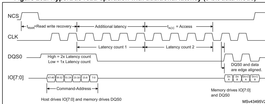
This timing diagram illustrates the HyperBus read operation with additional latency in 8-bit data mode. It shows four signal lines: NCS (active low), CLK (clock), DQS0 (data strobe), and IO[7:0] (data bus). The sequence starts with the NCS signal going low. The CLK signal is a periodic square wave. The DQS0 signal is initially high for 'Latency count 1' and then low for 'Latency count 2'. The IO[7:0] bus is driven by the host with command/address data (47:40, 39:32, 31:24, 23:16, 15:8, 7:0). After the command/address phase, the memory drives the DQS0 and IO[7:0] signals. The IO[7:0] bus shows data blocks Dn A, Dn B, Dn+1 A, and Dn+1 B. The timing parameters shown are \( t_{RWR} \) (Read write recovery), 'Additional latency', and \( t_{ACC} \) (Access). A note indicates that DQS0 and data are edge aligned. The diagram is labeled MSv43495V2.
Figure 203. HyperBus write operation with additional latency (8-bit data mode)
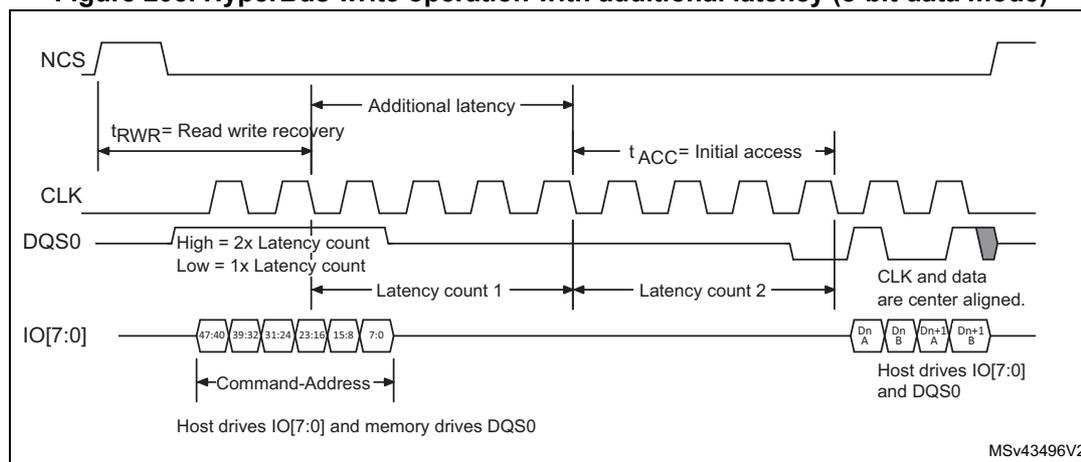
This timing diagram illustrates the HyperBus write operation with additional latency in 8-bit data mode. It shows four signal lines: NCS (active low), CLK (clock), DQS0 (data strobe), and IO[7:0] (data bus). The sequence starts with the NCS signal going low. The CLK signal is a periodic square wave. The DQS0 signal is initially high for 'Latency count 1' and then low for 'Latency count 2'. The IO[7:0] bus is driven by the host with command/address data (47:40, 39:32, 31:24, 23:16, 15:8, 7:0). After the command/address phase, the host continues to drive the IO[7:0] and DQS0 signals. The IO[7:0] bus shows data blocks Dn A, Dn B, Dn+1 A, and Dn+1 B. The timing parameters shown are \( t_{RWR} \) (Read write recovery), 'Additional latency', and \( t_{ACC} \) (Initial access). A note indicates that CLK and data are center aligned. The diagram is labeled MSv43496V2.
Fixed latency mode
Some devices or some applications may not want to operate with a variable latency time as described above.
The latency can be forced to \( 2 \times t_{ACC} \) by setting LM of XSPI_HLCR.
In this XSPI latency mode, the state of the DQS signal is not taken into account by the XSPI and an additional latency is always added leading to a fixed \( 2 \times t_{ACC} \) latency time.
Write operation with no latency
Some devices can also require a zero latency for the write operations. This write-zero latency can be forced by setting WZL in XSPI_HLCR.
Figure 204. HyperBus write operation with no latency (register write)
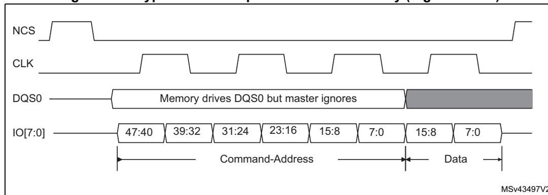
The diagram shows four signal lines over time: NCS (active low), CLK (square wave), DQS0 (data strobe), and IO[7:0] (data bus). - NCS goes low to initiate the write and returns high after the data is sent. - CLK provides the timing reference. - DQS0 is driven by the memory but ignored by the master. - IO[7:0] shows a sequence of 8-bit data: 47:40, 39:32, 31:24, 23:16, 15:8, 7:0, 15:8, 7:0. - The first six bytes (47:40 to 7:0) are labeled as 'Command-Address'. - The last two bytes (15:8, 7:0) are labeled as 'Data'. - A note indicates 'Memory drives DQS0 but master ignores'.
Latency on page-crossing during the read operations
An additional latency can be needed by some devices for the read operation when crossing pages.
The initial latency must be respected for any page access, as a consequence, when the first access is close to the page boundary, a latency is automatically added at the page crossing to respect the \( t_{ACC} \) time.
Figure 205. HyperBus read operation page crossing with latency (8-bit data mode)
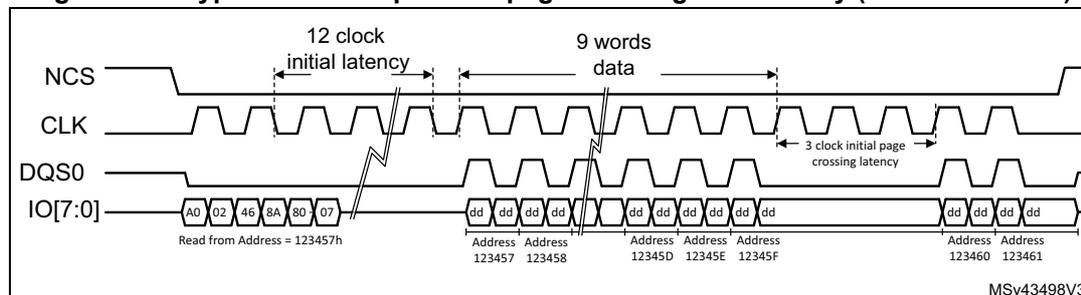
The diagram shows four signal lines over time: NCS, CLK, DQS0, and IO[7:0]. - NCS goes low to initiate the read. - CLK provides the timing reference. - DQS0 is driven by the memory. - IO[7:0] shows data being read: A0, 02, 46, 8A, 80, 07. Below this, it says 'Read from Address = 123457h'. - A '12 clock initial latency' is shown between the start of the read and the first data byte. - The data is then shown in groups of 8 bytes labeled 'dd'. - These are associated with addresses: Address 123457, Address 123458, Address 12345D, Address 12345E, Address 12345F, Address 123460, Address 123461. - A '9 words data' period is indicated. - A '3 clock initial page crossing latency' is shown when the address crosses from 12345F to 123460.
16-bit data transfer using HyperBus
In the HyperBus protocol, the XSPI supports a dual-octal configuration (16-bit data transfers) when DMM = 1 in XSPI_CR. In this configuration, one octal HyperBus memory is connected to IO0-IO7, and another is connected to IO8-IO15, following the same principle as the dual-octal configuration described in the regular command protocol. These memories share all signals except DQS, which are dedicated.
For 16-bit data transfers, DMODE[2:0] must be equal to 101. Any other value in DMODE[2:0] correspond to 8-bit data transfer (quad-, dual-, and single-bit data transfer do not exist in HyperBus protocol). Command-address phase is always using 8 bits in HyperBus protocol (from IO8-IO15). Only the data is on 16-bit for write or read operations accessing the memory space (from IO0-IO15) as shown for instance in Figure 206 . For the memory register accesses, the data is on 8-bit (from IO0 to IO7, IO8 to IO15 being not used but driven by the controller) as shown in Figure 204 .
The behavior of the interface at protocol-level is exactly the same as for HyperBus octal configuration, as described above, except that the variable latency is not supported in dual-octal HyperBus configuration. LM in XSPI_HLCR must be set.
Figure 206. HyperBus write operation with initial latency (16-bit mode)
![Timing diagram for HyperBus write operation with initial latency (16-bit mode). The diagram shows four signals: NCS (active-low chip select), CLK (clock), DQS[1:0] (data strobe), and IO[15:0] (data bus). NCS is shown as a pulse. CLK is a periodic square wave. DQS[1:0] is a signal that is high for 2x latency count and low for 1x latency count. IO[15:0] is shown as a sequence of 16-bit words: 47:40, 39:32, 31:24, 23:16, 15:8, 7:0. The first six words are labeled 'Command-Address'. The last two words are labeled 'Dn A', 'Dn B', 'Dn+1 A', 'Dn+1 B'. The diagram indicates that the host drives IO[15:0] and memory drives DQS[1:0]. Command-Address are sent on IO[7:0]. IO[15:8] are unused and driven H or L by the host. The diagram also shows the relationship between t_RWR (Read Write Recovery), t_ACC (Access), and Latency count. A note indicates that CLK and data are center aligned. The diagram is labeled MSV71532V2.](/RM0477-STM32H7Rx-7Sx/fb484f25720cbb3a73e4e8c242e67d73_img.jpg)
MSV71532V2
24.4.8 Specific features
The XSPI supports some specific features, such as:
- • wrap support
- • NCS boundary and refresh
- • communication regulation
Wrap support
The XSPI supports an hybrid wrap as defined by the HyperBus protocol. A hybrid wrap is also supported in the regular-command protocol.
In hybrid wrap, the transaction can continue after the initial wrap with an incremental access.
The wrap size supported by the target memory is configured by WRAPSIZE in XSPI_DCR2.
Wrap is supported only in memory-read direction and only for data size = 8 bytes. Wrapped reads are supported for both HyperBus and regular-command protocols. To enable wrapped-read accesses, the dedicated registers XSPI_WPxxx must be programmed according to the wrapped-read access characteristics. The dedicated XSPI_WPxxx registers apply for both HyperBus and regular-command protocols.
If the target memory is not supporting the hybrid wrap, WRAPSIZE must be set to 0.
Note: Hybrid wrap requires that the nonwrapped registers (XSPI_CCR, XSPI_TCR, XSPI_IR) are set according to the memory configuration to satisfy its correct data prefetch (initiated after the wrap command).
The wrap operation cannot be interrupted by a refresh. The refresh event is only considered after the wrap completion.
NCS boundary and refresh
Two processes can be activated to regulate the XSPI transactions:
- • NCS boundary
- • refresh
The NCS boundary feature limits a transaction to a boundary of aligned addresses. The size of the address to be aligned with is configured in CSBOUND[4:0] of XSPI_DCR3 and it is equal to \( 2^{\text{CSBOUND}} \) .
As an example, if CSBOUND[4:0] = 0x4, the boundary is set to \( 2^4 = 16 \) bytes. As a consequence, the NCS is released each time that the LSB address is equal to 0xF, and each time that a new transaction is issued to address the next data.
If CSBOUND[4:0] = 0, the feature is disabled. A minimum value of three is recommended.
The NCS boundary feature cannot be used for flash memory devices in write mode since a command is necessary to program another page of the flash memory.
The refresh feature limits the duration of the transactions to the value programmed in REFRESH[31:0] of XSPI_DCR4. The duration is expressed in number of cycles. This allows an external RAM to perform its internal refresh operation regularly.
The refresh value must be greater than the minimal transaction size in terms of number of cycles including the command, address, alternate/dummy phases.
If NCS boundary and refresh are enabled at the same time, the NCS is released on the first condition met.
Communication regulation
The communication regulation feature is useful in case two or more XSPIs share access to the same I/O port through an I/O manager. This feature limits the maximum length of a transaction to the value programmed in MAXTRAN[7:0] of XSPI_DCR3.
If the number of clock cycles of XSPI1 for example reach the MAXTRAN + 1 value, and if the second interface connected to the I/O manager requests an access, the NCS is released, and a new transaction is issued. If the second interface connected to the I/O manager does not request an access, the transaction is not stopped, and the NCS is not released.
If MAXTRAN[7:0] = 0, no limitation occurs.
The MAXTRAN[7:0] value must be greater than the minimal transaction size in terms of number of cycles including the command, address, alternate, and dummy phases.
Note: The communication regulation feature cannot be used in write mode for the flash memory devices that require extra command to reenable the write operation after the NCS is active again.
If NCS boundary, refresh and communication regulation are enabled at the same time, the NCS is released on the first condition met.
Restarting after an interrupted transfer
When a read or write operation is interrupted by a timeout, the XSPI interface, as soon as possible after getting back the port ownership, re-issues the initial command sequence together with the address following the last address actually accessed before interruption. The transfer initially set goes on and ends seamlessly.
24.4.9 XSPI operating modes introduction
The XSPI has the following operating modes regardless of the low-level protocol used (either regular-command or HyperBus):
- • indirect mode (read or write)
- • automatic status-polling mode (only in regular-command protocol)
- • memory-mapped mode
24.4.10 XSPI indirect mode
In indirect mode, the commands are started by writing to the XSPI registers, and the data is transferred by writing or reading the data register, in a similar way to other communication peripherals.
When FMODE[1:0] = 00 in XSPI_CR, the XSPI is in indirect-write mode: bytes are sent to the external device during the data phase. Data are provided by writing to XSPI_DR.
When FMODE[1:0] = 01, the XSPI is in indirect-read mode: bytes are received from the external device during the data phase. Data are recovered by reading XSPI_DR.
In indirect mode, when the XSPI is configured in DTR mode over eight lanes with DQS disabled, the given starting address and the data length must be even.
Note: The XSPI_AR register must be updated even if the start address is the same as the start address of the previous indirect access.
The number of bytes to be read/written is specified in XSPI_DLR:
- • If DL[31:0] = 0xFFFF FFFF, the data length is considered undefined and the XSPI simply continues to transfer data until it reaches the end of the external device (as defined by DEVSIZE). If no bytes are to be transferred, DMODE[2:0] must be set to 0 in XSPI_CCR.
- • If DL[31:0] = 0xFFFF FFFF and DEVSIZE[4:0] = 0x1F (its maximum value indicating at 4-Gbyte device), the transfers continue indefinitely, stopping only after an abort request or after the XSPI is disabled. After the last memory address is read (at address 0xFFFF FFFF), reading continues with address = 0x0000 0000.
When the programmed number of bytes to be transmitted or received is reached, TCF bit is set in XSPI_SR and an interrupt is generated if TCIE = 1 in XSPI_CR. In the case of an undefined number of data, TCF is set when the limit of the external SPI memory is reached, according to the device size defined in XSPI_DCR1.
Triggering the start of a transfer in regular-command protocol
Depending on the XSPI configuration, there are three different ways to trigger the start of a transfer in indirect mode when using regular-command protocol. In general, the start of transfer is triggered as soon as the software gives the last information that is necessary for the command. More specifically in indirect mode, a transfer starts when one of the following sequence of events occurs:
- • if no address is necessary (ADMODE[2:0] = 000) and if no data needs to be provided by the software (FMODE[1:0] = 01 or DMODE[2:0] = 000), and at the moment when a write is performed to INSTRUCTION[31:0] in XSPI_IR
- • if an address is necessary (when ADMODE[2:0] ≠ 000) and if no data needs to be provided by the software (when FMODE[1:0] = 01 or DMODE[2:0] = 000), and at the moment when a write is performed to ADDRESS[31:0] in XSPI_AR
- • if data needs to be provided by the software (when FMODE[1:0] = 00 and DMODE[2:0] ≠ 000), and at the moment when a write is performed to DATA[31:0] in XSPI_DR
A write to XSPI_ABR never triggers the communication start. If alternate bytes are required, they must have been programmed before.
As soon as a command is started, the BUSY bit is automatically set in XSPI_SR.
Triggering the start of a transfer in HyperBus protocol
Depending on the XSPI configuration, there are different ways to trigger the start of a command in indirect mode. In general, it is triggered as soon as the firmware gives the last information that is necessary for the transfer to start, and more specifically, a communication in indirect mode is triggered by one of the following register settings, when it is the last one to be executed:
- • when a write is performed to ADDRESS[31:0] (XSPI_AR) with ADMODE[2:0] ≠ 000 in indirect read mode (FMODE[1:0] = 01)
- • when a write is performed to DATA[31:0] (XSPI_DR) in indirect-write mode (when FMODE = 00)
- • when a (dummy) write is performed to INSTRUCTION[31:0] (XSPI_IR) for indirect read mode (with ADMODE[2:0] = 000 and FMODE = 01)
As soon as a transfer is started, the BUSY bit (XSPI_SR[5]) is automatically set.
FIFO and data management
Data in indirect mode pass through a 32-byte FIFO that is internal to the XSPI. FLEVEL in XSPI_SR indicates how many bytes are currently being held in the FIFO.
In indirect-write mode (FMODE[1:0] = 00), the software adds data to the FIFO when it writes in the XSPI_DR. A word write adds 4 bytes to the FIFO, a half-word write adds 2 bytes, and a byte write adds only 1 byte. If the software adds too many bytes to the FIFO (more than indicated in DL[31:0]), the extra bytes are flushed from the FIFO at the end of the write operation (when TCF is set).
The byte/half-word accesses to the XSPI_DR must be done only to the least significant byte/halfword of the 32-bit register.
FTHRES is used to define a FIFO threshold after which point the FIFO threshold flag, FTF, gets set. In indirect-read mode, FTF is set when the number of valid bytes to be read from the FIFO is above the threshold. FTF is also set if there is any data left in the FIFO after the last byte is read from the external device, regardless of FTHRES setting. In indirect-write mode, the FTF is set when the number of empty bytes in the FIFO is above the threshold.
If FTIE = 1, there is an interrupt when the FTF is set. If DMAEN = 1, a DMA transfer is initiated when the FTF is set. The FTF is cleared by hardware as soon as the threshold condition is no longer true (after enough data has been transferred by the CPU or DMA).
In indirect-read mode, when the FIFO becomes full, the XSPI temporarily stops reading bytes from the external device to avoid an overrun.
The last data read in RX FIFO remains valid as long as there is no request for the next line. This means that, when the application reads several times in a row at the same location, the data is provided from the RX FIFO and not read again from the distant memory.
24.4.11 XSPI automatic status-polling mode
In automatic status-polling mode, the XSPI periodically starts a command to read a defined number of status bytes (up to four). The received bytes can be masked to isolate some status bits and an interrupt can be generated when the selected bits have a defined value.
The automatic status-polling mode must be used only in regular-command protocol. For HyperBus protocol, it is not exploitable since the read status register into the HyperFlash memory must be performed in two steps (a write operation followed by a read operation).
The access to the device begins in the same manner as in indirect-read mode. BUSY in XSPI_SR goes high at this point, and stays high even between the periodic accesses.
The content of MASK[31:0] in XSPI_PSMAR is used to mask the data from the external device in automatic status-polling mode:
- • If the MASK[n] = 0, then bit n of the result is masked and not considered.
- • If MASK[n] = 1, and the content of bit[n] is the same as MATCH[n] in XSPI_PSMAR, then there is a match for bit n.
If PMM = 0 in XSPI_CR, the AND-match mode is activated: SMF is set in XSPI_SR only when there is a match on all of the unmasked bits.
If PMM = 1 in XSPI_CR, the OR-match mode is activated: SMF gets set if there is a match on any of the unmasked bits.
An interrupt is called when SMF = 1 if SMIE = 1.
If APMS is set in XSPI_CR, the operation stops and BUSY goes to 0 as soon as a match is detected. Otherwise, BUSY stays at 1 and the periodic accesses continue until there is an abort or until the XSPI is disabled (EN = 0).
XSPI_DR contains the latest received status bytes (FIFO deactivated). The content of this register is not affected by the masking used in the matching logic. FTF in XSPI_SR is set as soon as a new reading of the status is complete. FTF is cleared as soon as the data is read.
In automatic status-polling mode, variable latency is not supported. As a consequence, the memory must be configured in fixed latency.
24.4.12 XSPI memory-mapped mode
When configured in memory-mapped mode, the external SPI device is seen as an internal memory.
Note: No more than 256 Mbytes can be addressed even if the external device capacity is larger.
If an access is made to an address outside of the range defined by DEVSIZE[4:0] but still within the 256-Mbyte range, then an AXI error is given. The effect of this error depends on the AXI master that attempted the access:
- • If it is the Cortex CPU, a hard-fault interrupt is generated.
- • If it is a DMA, a DMA transfer error is generated, and the corresponding DMA channel is automatically disabled.
Byte, half-word, and word access types are all supported.
A support for execute in place (XIP) operation is implemented, where the XSPI continues to load the bytes to the addresses following the most recent access. If subsequent accesses are continuous to the bytes that follow, then these operations end up quickly since their results were prefetched.
By default, the XSPI never stops its prefetch operation, it either keeps the previous read operation active with the NCS maintained low or it relaunches a new transfer, even if no access to the external device occurs for a long time.
Since external devices tend to consume more power when the NCS is held low, the application may want to activate the timeout counter (TCEN = 1 in XSPI_CR): the NCS is released after a period defined by TIMEOUT[15:0] in XSPI_LPTR, when x cycles have elapsed without an access since the clock is inactive.
BUSY goes high as soon as the first memory-mapped access occurs. Because of the prefetch operations, BUSY does not fall until there is an abort, or the peripheral is disabled.
It is not recommended to program the flash memory using the memory-mapped writes. The indirect-write mode fulfills this operation.
However, if the application requires the use of the MCE for encryption (check MCE product availability), the memory-mapped write mode may be used to program encrypted data to external flash memory under the following conditions:
- • Prefetch must be enabled.
- • In block cipher mode, the CPU must write a complete 128-bit data block to prevent the MCE from initiating read-modify-write operations when only a few bytes need to be programmed. This precaution avoids incorrect programming operations. There are no specific constraints to respect if the MCE is used in stream cipher mode.
- • Apply the abort sequence to exit memory-mapped mode when the data linked to the page has been written in the external memory buffers. The abort sequence triggers the start of the page programming.
- • Switch to the automatic status-polling mode to monitor the completion of the page programming phase.
- • Relaunch the write enable command in indirect mode, then switch back to the memory-mapped mode configuration to continue to program additional pages if any.
It is recommended to add a synchronization barrier between the end of the controller registers configuration and the first memory-mapped access to the external memory when the controller is configured in memory-mapped mode.
24.4.13 XSPI configuration introduction
The XSPI configuration is done in three steps:
- 1. XSPI system configuration
- 2. XSPI device configuration
- 3. XSPI mode configuration
24.4.14 XSPI system configuration
The XSPI is configured using XSPI_CR. The user must program:
- • the functional mode with FMODE[1:0]
- • the automatic status-polling mode behavior if needed with PMM and APMS
- • the FIFO level with FTHRES
- • DMA use with DMAEN
- • the timeout counter use with TCEN
- • the dual-memory configuration, if needed, with DMM
In case of an interrupt use, the respective enable bit can also be set during this phase.
If the timeout counter is used, the timeout value is programmed in XSPI_LPTR.
The DMA channel must not be enabled during the XSPI configuration: it must be enabled only when the operation is fully configured, to avoid any unexpected request generation.
The DMA and XSPI must be configured in a coherent manner regarding data length: FTHRES value must reflect the DMA burst size.
24.4.15 XSPI device configuration
The parameters related to the external device targeted are configured through XSPI_DCR1 and XSPI_DCR2. The user must program:
- • the device size with DEVSIZE[4:0]
- • the chip-select minimum high time with CSHT[5:0]
- • the device frequency with PRESCALER[7:0]
DEVSIZE[4:0] defines the size of external memory using the following formula:
where DEVSIZE+1 is the number of address bits required to address the external device. The external device capacity can go up to 4 Gbytes (addressed using 32 bits) in indirect mode, but the addressable space in memory-mapped mode is limited to 256 Mbytes.
If DMM = 1, DEVSIZE[4:0] must reflect the total capacity of the two devices together considering the above formula (DEVSIZE[4:0] value is so equal to one of the two memory capacities).
When the XSPI executes two commands, one immediately after the other, it raises the NCS high between the two commands, at least one CLK cycle by default.
If the external device requires more time between commands, CSHT[5:0] can be used to specify the minimum number of CLK cycles (up to 64) for which the NCS must remain high.
CKMODE indicates the level that the CLK takes between commands (when NCS = 1).
In HyperBus protocol, the device timing ( \( t_{ACC} \) and \( t_{RWR} \) ) and the Latency mode must be configured in XSPI_HLCR.
Memory types
External memory providers may have architecture and slight data formatting differences. The bitfield MTYP[2:0] into the XSPI_CR register allows targeting the right controller configuration depending on the associated memory type selected in the application. It is the responsibility of the software developer to align the controller configuration to fit with the targeted memory type.
The memory types are grouped in this way:
- • D0/D1 data ordering in octal-SPI data mode (DMODE[2:0] = 100) in DTR mode by configuring MTYP[2:0] = 000. For instance, Micron is using such data ordering. In this configuration, the DQS is sent with a polarity inverted respect to the clock polarity.
Figure 207. D0/D1 data ordering in octal-SPI DTR mode (Micron) - Read access
![Timing diagram for Figure 207 showing NCS, CLK, DQS, and IO[7:0] signals. The IO[7:0] signal shows a sequence of EEh, 11h, A31:24, A23:16, A15:8, A7:0 (Address), followed by a Dummy phase, and then data Word units D0, D1, D2, D3. The diagram is labeled MSV71558V1.](/RM0477-STM32H7Rx-7Sx/54fe73eddfa95d4e0d6cd3b645d9e47f_img.jpg)
- • D1/D0 data ordering in octal-SPI data mode (DMODE[2:0] = 100) in DTR mode by configuring MTYP[2:0] = 001. For instance, Macronix is using this reverse data ordering in its Octaflash portfolio (this configuration is not adapted to its OctaRAM™ memories). DQS is keeping the same polarity as the clock when reading data from the memory. Refer to Figure 197: DTR read in octal-SPI mode with DQS (Macronix mode) example .
- • D1/D0 data ordering in octal-SPI data mode (DMODE[2:0] = 100) in DTR mode by configuring MTYP[2:0] = 011 with specific address phase built with row and column to fit with Macronix OctaRAM™ memories requirement (refer to Table 212: OctaRAM command address bit assignment (based on 64 Mb OctaRAM) ). This is the controller which translates internally the targeted address provided by the software in row/column address formatting to sent to the memory. DQS is keeping the same polarity as the clock when reading data from the memory.
Figure 208. OctaRAM read operation with reverse data ordering D1/D0
![Timing diagram for Figure 208 showing NCS, CLK, DQS, and IO[7:0] signals. The IO[7:0] signal shows a sequence of Command, Raw address, Column address (Command & Address), followed by data Word units D1, D0, D3, D2. The diagram is labeled MSV71560V1.](/RM0477-STM32H7Rx-7Sx/6ecd096e1f7e8f80277286d932d8be6a_img.jpg)
(based on 64 Mb (1) OctaRAM)
| Clock | 1st clock | 2nd clock | 3rd clock | ||
|---|---|---|---|---|---|
| Function | Command | Row address | Column address | ||
| SIO[7] | Command | Reserved | RA7 | CA9 | Reserved |
| SIO[6] | Reserved | RA6 | CA8 | Reserved | |
| SIO[5] | Reserved | RA5 | CA7 | Reserved | |
| SIO[4] | RA12 | RA4 | CA6 | Reserved | |
| SIO[3] | RA11 | RA3 | CA5 | CA3 | |
| SIO[2] | RA10 | RA2 | CA4 | CA2 | |
| SIO[1] | RA9 | RA1 | Reserved | CA1 | |
| SIO[0] | RA8 | RA0 | Reserved | CA0 (2) | |
1. Example of 64 Mb OctaRAM address assignment:
Row Address [RA12:RA0]: 8K. Column address [CA9:CA0]: 1K. 64 Mb density = 8K x 1K x 8 bits
2. Column address A0 must be always 0.
- HyperBus memories need to be selected when targeted by the application. The configuration to set depends on the access type:
- HyperBus memory mode: The protocol follows the HyperBus specification. MTYP[2:0] = 100 is the configuration to use to access the memory space.
- HyperBus register mode (addressing register space): the memory-mapped accesses in this mode must be noncacheable, or the indirect read/write modes must be used. The configuration to be set for this particular register space access is MTYP[2:0] = 101.
- The software must configure MTYP[2:0] = 110 when the memory targeted comes from APmemory and DMODE[2:0] = 101 to fit with the memory provider requirements concerning the address formatting.
- Standard mode. It is the mode to use whenever the targeted memory is not corresponding to any others configurations described in this section. MTYP[2:0] = 010 for this standard mode.
24.4.16 XSPI regular-command mode configuration
Indirect mode configuration
When FMODE[1:0] = 00, the indirect-write mode is selected and data can be sent to the external device. When FMODE[1:0] = 01, the indirect-read mode is selected and data can be read from the external device.
When the XSPI is used in indirect mode, the frames are constructed in the following way:
- Specify a number of data bytes to read or write in XSPI_DLR.
- Specify the frame timing in XSPI_TCR.
- Specify the frame format in XSPI_CCR.
- Specify the instruction in XSPI_IR.
- 5. Specify the optional alternate byte to be sent right after the address phase in XSPI_ABR.
- 6. Specify the targeted address in XSPI_AR.
- 7. Enable the DMA channel if needed.
- 8. Read/write the data from/to the FIFO through XSPI_DR (if no DMA usage).
If neither the address register (XSPI_AR) nor the data register (XSPI_DR) need to be updated for a particular command, then the command sequence starts as soon as XSPI_IR is written. This is the case when both ADMODE[2:0] and DMODE[2:0] equal 000, or if just ADMODE[2:0] = 000 when in indirect-read mode (FMODE[1:0] = 01).
When an address is required (ADMODE[2:0] ≠ 000) and the data register does not need to be written (FMODE[1:0] = 01 or DMODE[2:0] = 000), the command sequence starts as soon as the address is updated with a write to XSPI_AR.
In case of data transmission (FMODE[1:0] = 00 and DMODE[2:0] ≠ 000), the communication start is triggered by a write in the FIFO through XSPI_DR.
Automatic status-polling mode configuration
The automatic status-polling mode is enabled by setting FMODE[1:0] = 10. In this mode, the programmed frame is sent and the data is retrieved periodically.
The maximum amount of data read in each frame is 4 bytes. If more data is requested in XSPI_DLR, it is ignored, and only 4 bytes are read. The periodicity is specified in XSPI_PIR.
Once the status data has been retrieved, the following can be processed:
- • Set SMF (an interrupt is generated if enabled).
- • Stop automatically the periodic retrieving of the status bytes.
The received value can be masked with the value stored in XSPI_PSMKR, and can be ORed or ANDed with the value stored in XSPI_PSMAR.
In case of a match, SMF is set and an interrupt is generated if enabled. The XSPI can be automatically stopped if AMPS is set. In any case, the latest retrieved value is available in XSPI_DR.
When the XSPI is used in automatic status-polling mode, the frames are constructed in the following way:
- 1. Specify the input mask in XSPI_PSMKR.
- 2. Specify the comparison value in XSPI_PSMAR.
- 3. Specify the read period in XSPI_PIR.
- 4. Specify a number of data bytes to read in XSPI_DLR.
- 5. Specify the frame timing in XSPI_TCR.
- 6. Specify the frame format in XSPI_CCR.
- 7. Specify the instruction in XSPI_IR.
- 8. Specify the optional alternate byte to be sent right after the address phase in XSPI_ABR.
- 9. Specify the optional targeted address in XSPI_AR.
If the address register (XSPI_AR) does not need to be updated for a particular command, then the command sequence starts as soon as XSPI_CCR is written. This is the case when ADMODE[2:0] = 000.
When an address is required (ADMODE[2:0] ≠ 000), the command sequence starts as soon as the address is updated with a write to XSPI_AR.
Memory-mapped mode configuration
In memory-mapped mode, the external device is seen as an internal memory but with some latency during accesses. Read and write operations are allowed to the external device in this mode.
It is not recommended to program the flash memory using memory-mapped writes, as the internal flags for erase or programming status have to be polled. The indirect-write mode fulfills this operation, possibly in conjunction with the automatic status-polling mode.
Memory-mapped mode is entered by setting FMODE[1:0] = 11 in XSPI_CR.
The programmed instruction and frame are sent when an AXI master accesses the memory mapped space.
The FIFO is used as a prefetch buffer to anticipate any linear reads. Any access to XSPI_DR in this mode returns zero.
The data length register (XSPI_DLR) has no meaning in memory-mapped mode.
When the XSPI is used in memory-mapped mode, the frames are constructed in the following way:
- 1. Specify the frame timing in XSPI_TCR for read operation.
- 2. Specify the frame format in XSPI_CCR for read operation.
- 3. Specify the instruction in XSPI_IR.
- 4. Specify the optional alternate byte to be sent right after the address phase in XSPI_ABR for read operation.
- 5. Specify the frame timing in XSPI_WTCR for write operation.
- 6. Specify the frame format in XSPI_WCCR for write operation.
- 7. Specify the instruction in XSPI_WIR.
- 8. Specify the optional alternate byte to be sent right after the address phase in XSPI_WABR for write operation.
All the configuration operations must be completed (ensured by checking BUSY = 0) before the first access to the memory area: any register write operation when BUSY = 1 have no effect and is not signaled with an error response. On the first access, the XSPI becomes busy, and no further configuration is allowed. Then, the only way to get BUSY low is to clear the ENABLE bit or to abort by setting the ABORT bit.
Memory-mapped write operations are not supported without write strobe.
XSPI delayed data sampling when no DQS is used
By default, when no DQS is used, the XSPI samples the data driven by the external device one half of a CLK cycle after the external device drives the signal.
In case of any external signal delays, it may be useful to sample the data later. Using SSHIFT in XSPI_TCR, the sampling of the data can be shifted by half of a CLK cycle.
The firmware must clear SSHIFT when the data phase is configured in DTR mode (DDTR = 1).
XSPI delayed data sampling when DQS is used
When external DQS is used as a sampling clock, it is shifted precisely by one quarter of the SPI clock cycle, for all frequencies above
freq_min
, to compensate the data propagation delay in the “high-speed interface” when the product embeds one.
24.4.17 XSPI HyperBus protocol configuration
Indirect mode configuration (HyperBus)
When
FMODE[1:0] = 00
, the indirect-write mode is selected and data can be sent to the external device. When
FMODE[1:0] = 01
, the indirect-read mode is selected where data can be read from the external device.
ADMODE
must be configured with a value different from 000 (for instance
ADMODE = 100
).
When the XSPI is used in indirect mode, the frames are constructed in the following way:
- 1. Specify a number of data bytes to read or write in
XSPI_DLR. - 2. Specify the targeted address in
XSPI_AR. - 3. Enable the DMA channel if needed.
- 4. Read/write the data from/to the FIFO through
XSPI_DR(if no DMA usage).
In indirect-read mode, the command sequence starts as soon as the address is updated with a write to
XSPI_AR
.
In indirect-write mode, the communication start is triggered by a write in the FIFO through
XSPI_DR
.
Memory-mapped mode configuration (HyperBus)
In memory-mapped mode, the external device is seen as an internal memory but with some latency during the accesses. Read and write operations are allowed to the external device in this mode.
It is not recommended to program the flash memory using the memory-mapped writes: the indirect-write mode fulfills this operation.
The memory-mapped mode is entered by setting
FMODE[1:0] = 11
. The programmed instruction and frame is sent when an AXI master is accessing the memory mapped space.
The FIFO is used as a prefetch buffer to anticipate any linear reads. Any access to
XSPI_DR
in this mode returns zero.
The data length register (
XSPI_DLR
) has no meaning in memory-mapped mode.
All the configuration operation must be completed before the first access to the memory area. On the first access, the XSPI becomes busy, and no configuration is allowed. Then, the only way to get BUSY low is to clear the ENABLE bit or to abort by setting the ABORT bit.
24.4.18 XSPI error management
The following errors set the TEF flag in
XSPI_SR
and generates an interrupt if enabled (
TEIE = 1
in
XSPI_CR
):
- • in indirect or automatic status-polling mode, when a wrong address has been programmed in
XSPI_AR(according to the device size defined byDEVSIZE[4:0]).
- • in indirect mode, if the address plus the data length exceed the device size. TEF is set as soon as the access is triggered.
In memory-mapped mode, the XSPI generates an AXI slave error in the following situations:
- • The memory-mapped mode is disabled and an AXI read or write request occurs.
- • Read or write address exceeds the size of the external memory.
- • Abort is received while a read or write burst is ongoing when the abort condition is present at the moment of transfer phases preceding the data phase (In incremental or wrap burst type modes). To avoid the error, refer to Section 24.4.20: XSPI BUSY and ABORT .
- • The XSPI is disabled while a read or write burst is requested.
- • A write wrap burst is received.
- • A write request is received while DQSE = 0 in XSPI_WCCR in octal DTR mode, in dual-memory configuration, in hyperbus mode or 16-bit mode.
- • A read or write request is received while DMODE[2:0] = 000 (no data phase), except when MTYP[2:0] is HyperBus.
- • Illegal access size when wrap read burst. This means AXI Bus transfer size (ARSIZE) is different from 8 bytes (only for memory-mapped mode).
- • Bit DMM is set in XSPI_CR (dual-memory configuration) and 16-bit mode is set.
24.4.19 XSPI high-speed interface and calibration
To reach higher frequencies, a dedicated high-speed interface is inserted between the XSPI (or the I/O manager in case the product embeds one), and the I/O pads.
The following is valid for all data bus sizes 1, 2, 4, 8 or 16 bits.
The high-speed interface block embeds resynchronization registers that are clocked by a delayed clock created from a DLL (delay locked loop) also located in the high-speed interface. The high-speed interface features are controlled by registers located in the XSPI.
The purpose of resynchronization is primary to shift data or data strobe by one quarter of controller bus clock period, with a correct timing accuracy. DLL must be calibrated versus this clock period.
The calibration process is automatically enabled when one of the three conditions below is met:
- • The XSPI exits reset state.
- • A value is written in PRESCALER[7:0] of XSPI_DCR2.
- • A value is written in XSPI_CCR.
The calibration process starts when the two following conditions are both met:
- • The calibration has been enabled by one of the three conditions above.
- • An action that sets BUSY = 1 is performed. For example the first transfer to memory after calibration is enabled. When the calibration is completed, BUSY returns to 0.
In case a periodic recalibration is needed (for example to take in account possible variations in temperature or power supply on a long duration), this recalibration must be triggered by writing periodically in PRESCALER[7:0] of XSPI_DCR2, while BUSY = 0.
Once the calibration is completed, the value of the SPI bus clock period, expressed in number of unitary delay, is available to user in COARSE[5:0] and FINE[6:0] of XSPI_CALFCR.
After auto-calibration, XSPI_CALSOR and XSPI_CALSIR are automatically loaded with the same value that corresponds to the delay for a quarter cycle.
The automatic calibration is not executed if at least one of both registers XSPI_CALSOR/XSPI_CALSIR is written between the last write operation on XSPI_DCR2 or XSPI_CCR and the next transfer start. In such case, the calibration values must be set by the software code into XSPI_CALSOR and XSPI_CALSIR registers. It may improve the flash programming time without relaunching the automatic calibration processing between two programming pages.
When the memory is not supporting DQS (DQSE = 0), the automatic calibration is not used in reception. The DLL Master is used instead for delaying the feedback clock (XSPI_CALMR). This delay needs to be adjusted by the application itself, using a software sequence that determines which delay is optimal to guarantee the correct read operations.
When the clock is divided in DTR transmission mode, the quarter cycle delays on DQS/data are not inserted by the DLLs themselves, but by internal flops design scheme. In SDR transmission mode, the DLLs are not used and this, whatever the clock prescaler value.
In case of DTR mode and prescaler bypassed (PRESCALER[7:0] = 0), the kernel clock provided to interface must have a 50 % duty-cycle.
When using the high-speed-interface, the system clock (AXI clock) must be at least as fast as the SPI clock.
24.4.20 XSPI BUSY and ABORT
Once the XSPI starts an operation with the external device, BUSY is automatically set in XSPI_SR.
In indirect mode, BUSY is reset once the XSPI has completed the requested command sequence and the FIFO is empty.
In automatic status-polling mode, BUSY goes low only after the last periodic access is complete, due to a match when APMS = 1 or due to an abort.
After the first access in memory-mapped mode, BUSY goes low only on an abort.
Any operation can be aborted by setting ABORT in XSPI_CR. Once the abort is completed, BUSY and ABORT are automatically reset, and the FIFO is flushed.
Before setting ABORT, the software must ensure that all the current transactions are finished using the synchronization barriers. When DMA is enabled to handle the data read or write operations in XSPI_DR, it is recommended to disable the DMA channel before aborting the XSPI.
Note: Some devices may misbehave if a write operation to a status register is aborted.
24.4.21 XSPI reconfiguration or deactivation
Before any XSPI reconfiguration, the software must ensure that all the transactions are completed:
- • After a memory-mapped write, the software must perform a dummy read followed by a synchronization barrier, then an abort.
- • After a memory-mapped read, the software must perform a synchronization barrier then an abort.
24.4.22 NCS behavior
By default, NCS is high, deselecting the external device. NCS falls before an operation begins and rises as soon as it finishes.
When CKMODE = 0 (clock mode 0: CLK stays low when no operation is in progress), NCS falls one CLK cycle before an operation first rising CLK edge, and NCS rises one CLK cycle after the operation final rising CLK edge (see the figure below).
Figure 209. NCS when CKMODE = 0 (T = CLK period)
The diagram shows two signal lines, NCS and CLK. The CLK signal is a periodic square wave. The NCS signal is high initially. It falls one CLK cycle before the first rising edge of CLK. It remains low until after the final rising edge of CLK, then rises one CLK cycle later. The CLK period is labeled T. The diagram is labeled MSv44100V2.
When CKMODE = 1 (clock mode 3: CLK goes high when no operation is in progress) and when in SDR mode, NCS falls one CLK cycle before an operation first rising CLK edge, and NCS rises one CLK cycle after the operation final rising CLK edge (see the figure below).
Figure 210. NCS when CKMODE = 1 in SDR mode (T = CLK period)
The diagram shows two signal lines, NCS and CLK. The CLK signal is a periodic square wave. The NCS signal is high initially. It falls one CLK cycle before the first rising edge of CLK. It remains low until after the final rising edge of CLK, then rises one CLK cycle later. The CLK period is labeled T. The diagram is labeled MSv44101V2.
When the CKMODE = 1 (clock mode 3) and DDTR = 1 (data DTR mode), NCS falls one CLK cycle before an operation first rising CLK edge, and NCS rises one CLK cycle after the operation final active rising CLK edge (see the figure below). Because the DTR operations must finish with a falling edge, the CLK is low when NCS rises, and CLK rises back up one half of a CLK cycle afterwards.
Figure 211. NCS when CKMODE = 1 in DTR mode (T = CLK period)
The diagram shows two signal lines, NCS and CLK. The CLK signal is a periodic square wave. The NCS signal is high initially. It falls one CLK cycle before the first rising edge of CLK. It remains low until after the final active rising CLK edge, then rises one CLK cycle later. The CLK period is labeled T, and the time from the final active rising CLK edge to the NCS rising edge is labeled T/2. The diagram is labeled MSv44102V2.
When the FIFO stays full during a read operation, or if the FIFO stays empty during a write operation, the operation stalls and CLK stays low until the software services the FIFO. If an abort occurs when an operation is stalled, NCS rises just after the abort is requested and then CLK rises one half of a CLK cycle later (see the figure below).
Figure 212. NCS when CKMODE =1 with an abort (T = CLK period)
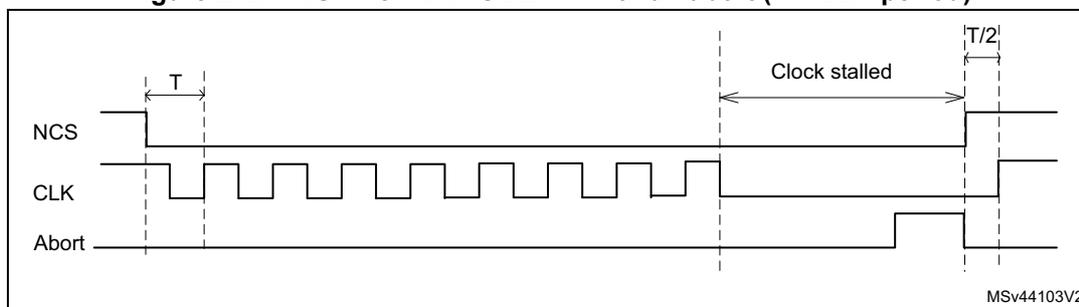
The diagram shows three signals over time: NCS (active low), CLK (clock), and Abort. - NCS starts high, goes low at time 0, and stays low until after the abort pulse. - CLK is a periodic square wave with period T. It stops toggling during the 'Clock stalled' period. - Abort is a pulse that goes high at time 0 and returns low at time T. - The 'Clock stalled' period begins when the abort pulse goes high and ends when CLK resumes toggling. - NCS rises to high just after the abort pulse goes high. - CLK resumes toggling (rises) at time T/2 after the abort pulse goes high. - Source: MSV44103V2
In dual-memory configuration, the NCS2 behaves exactly the same as the NCS1. The quad-SPI/octal-SPI memory 2 can then use the NCS1, and the NCS2 pin can be used for other functions.
24.4.23 Software control of two external memories
One XSPI instance is able to control the generation of the two chip-select signals (NCS1 and NCS2). This allows two external memories to be connected to the same I/O port driven by the XSPI.
The XSPI generates one NCS signal and the user defines how the NCS is directed to NCS1 or NCS2, by setting the CSSEL bit in XSPI_CR. Intended operation is semistatic commutation, such as starting an application reading an external flash memory and then, for the rest of the application, use an external SRAM connected to the same I/O bus. From a memory-map point of view, these two memories are located in the same address range.
Figure 213. Example of software control of two external memories
![Block diagram showing an STM32 microcontroller connected to two 16-bit memories via an XSPI interface. The XSPI block has pins for CLK, NCLK, DQS0, DQS1, NCS1, NCS2, and IO[15:0]. The CSSEL bit in XSPI_CR is used for software control. The first memory is connected to XSPIM_P1_CLK, XSPIM_P1_NCLK, XSPIM_P1_DQS0, XSPIM_P1_DQS1, XSPIM_P1_NCS1, and XSPIM_P1_IO[15:0]. The second memory is connected to XSPIM_P1_CLK, XSPIM_P1_NCLK, XSPIM_P1_DQS1, XSPIM_P1_NCS2, and XSPIM_P1_IO[15:0].](/RM0477-STM32H7Rx-7Sx/cc00587905bf75f0a3804b8c6efde3c5_img.jpg)
The diagram shows an STM32 microcontroller connected to two 16-bit memories via an XSPI interface. - The STM32 contains an XSPI block with a 'CSSEL in XSPI_CR' register. - The XSPI block has pins: XSPIM_P1_CLK, XSPIM_P1_NCLK, XSPIM_P1_DQS0, XSPIM_P1_DQS1, XSPIM_P1_NCS1, XSPIM_P1_NCS2, and XSPIM_P1_IO[15:0]. - 'Software control' is indicated for the CSSEL bit. - '16-bit memory 1' is connected to: clk (XSPIM_P1_CLK), nclk (XSPIM_P1_NCLK), Data strobe 1 (XSPIM_P1_DQS0), NCS (XSPIM_P1_NCS1), and Data[15:0] (XSPIM_P1_IO[15:0]). - '16-bit memory 2' is connected to: clk (XSPIM_P1_CLK), nclk (XSPIM_P1_NCLK), Data strobe 1 (XSPIM_P1_DQS1), Data strobe 2 (XSPIM_P1_NCS2), NCS (XSPIM_P1_NCS2), and Data[15:0] (XSPIM_P1_IO[15:0]). - Source: MSV67896V2
24.5 Address alignment and data number
The following table summarizes the effect of the address alignment and programmed data number depending on the use case.
Table 213. Address alignment cases
| Memory type | Transaction type | Constraint on address (1) | Impact if constraint on address not respected | Constraint on number of bytes (1) | Impact if constraint on bytes not respected |
|---|---|---|---|---|---|
| Single, dual, quad flash or SRAM (DMM = 0) | IND (2) read | None | None | None | None |
| MM (3) read | |||||
| IND write | |||||
| MM write | |||||
| Single, dual, quad flash or SRAM (DMM = 1) | IND read | Even | ADDR[0] is set to 0. (4) | Even | DLR[0] is set to 1. (5) |
| MM read | None | None | None | None | |
| IND write | Even | ADDR[0] is set to 0. (4) | Even | DLR[0] is set to 1. (5) | |
| MM write | Even | Slave error | Even | Last byte is lost. | |
| Octal flash in SDR mode | IND read | None | None | None | None |
| MM read | |||||
| IND write | |||||
| MM write | |||||
| Octal memory in DTR mode without WDM (6) , or 16-bit memory in SDR mode without WDM | IND read | Even | ADDR[0] is set to 0. (4) | Even | DLR[0] is set to 1. (5) |
| MM read | None | None | None | None | |
| IND write | Even | ADDR[0] is set to 0. (4) | Even | DLR[0] is set to 1. (5) | |
| MM write | Even | Slave error | Even | Last byte is lost. | |
| 16-bit or dual-octal memory in DTR mode without WDM | IND read 32-bit | Aligned | ADDR[1:0] is assumed to be 00. (4) | N × 4 | DLR[1:0] is assumed to be 11. (5) |
| MM read | None | None | None | None | |
| IND write | Aligned | ADDR[1:0] is assumed to be 00. (4) | N × 4 | DLR[1:0] is assumed to be 11. (5) | |
| MM write | Aligned | Slave error | N × 4 | Last byte is lost. | |
| Octal flash or RAM in DTR mode with WDM | IND read | Even | ADDR[0] is set to 0. (4) | Even | DLR[0] is set to 1. (5) |
| MM read | None | None | None | None | |
| IND write (7) | |||||
| MM write | |||||
| HyperBus | IND read | Even | ADDR[0] is set to 0. (4) | Even | DLR[0] is set to 1. (5) |
| MM read | None | None | None | None | |
| IND write (7) | |||||
| MM write |
Table 213. Address alignment cases (continued)
| Memory type | Transaction type | Constraint on address (1) | Impact if constraint on address not respected | Constraint on number of bytes (1) | Impact if constraint on bytes not respected |
|---|---|---|---|---|---|
| 16-bit data bus memory or dual-octal memory with WDM | IND read 32-bit | Aligned | ADDR[1:0] is assumed to be 00. (4) | N × 4 | DLR[1:0] is assumed to be 11. (5) |
| MM read | |||||
| IND write (8) | None | None | None | None | |
| MM write | |||||
| 16-bit HyperBus | IND read 32-bit | Aligned | ADDR[1:0] is assumed to be 00. (4) | N × 4 | DLR[1:0] is assumed to be 11. (5) |
| MM read | |||||
| IND write (9) | None | None | None | None | |
| MM write |
- 1. To be respected by the software.
- 2. IND = indirect mode.
- 3. MM = memory-mapped mode.
- 4. Extra data at transfer start.
- 5. Extra data at transfer end.
- 6. WDM = write data mask.
- 7. If the FTHRES bitfield is set to the maximum value with DLR value greater than the data burst length, and if the DMA is enabled or the interrupt based on FIFO THRESHOLD Flag is enabled (FTF), the address must be modulo 2 aligned in DTR mode when the initiator (DMA, CPU, ...) is writing the data with a burst length equal to the FIFO size.
- 8. If the FTHRES bitfield is set to the maximum value with DLR value greater than the data burst length, and if the DMA is enabled or the interrupt based on FIFO THRESHOLD Flag is enabled (FTF), the address must be modulo 4 aligned in DTR mode or modulo 2 in SDR mode when the initiator (DMA, CPU, ...) is writing the data with a burst length equal to the FIFO size.
- 9. If the FTHRES bitfield is set to the maximum value with DLR value greater than the data burst length, and if the DMA is enabled or the interrupt based on FIFO THRESHOLD Flag is enabled (FTF), the address must be modulo 4 aligned in DTR mode when the initiator (DMA, CPU, ...) is writing the data with a burst length equal to the FIFO size.
24.6 XSPI interrupts
An interrupt can be produced on the following events:
- • timeout
- • status match
- • FIFO threshold
- • transfer complete
- • transfer error
Separate interrupt enable bits are available to provide more flexibility.
Table 214. XSPI interrupt requests
| Interrupt event | Event flag | Enable control bit |
|---|---|---|
| Timeout | TOF | TOIE |
| Status match | SMF | SMIE |
Table 214. XSPI interrupt requests
| Interrupt event | Event flag | Enable control bit |
|---|---|---|
| FIFO threshold | FTF | FTIE |
| Transfer complete | TCF | TCIE |
| Transfer error | TEF | TEIE |
24.7 XSPI registers
24.7.1 XSPI control register (XSPI_CR)
Address offset: 0x000
Reset value: 0x0000 0000
| 31 | 30 | 29 | 28 | 27 | 26 | 25 | 24 | 23 | 22 | 21 | 20 | 19 | 18 | 17 | 16 |
|---|---|---|---|---|---|---|---|---|---|---|---|---|---|---|---|
| MSEL[1:0] | FMODE[1:0] | Res. | Res. | Res. | CSSEL | PMM | APMS | Res. | TOIE | SMIE | FTIE | TCIE | TEIE | ||
| rw | rw | rw | rw | rw | rw | rw | rw | rw | rw | rw | rw | ||||
| 15 | 14 | 13 | 12 | 11 | 10 | 9 | 8 | 7 | 6 | 5 | 4 | 3 | 2 | 1 | 0 |
| Res. | Res. | Res. | FTHRES[4:0] | Res. | DMM | Res. | Res. | TCEN | DMAEN | ABORT | EN | ||||
| rw | rw | rw | rw | rw | rw | rw | rw | rw | rw | ||||||
Bits 31:30 MSEL[1:0] : Flash select
These bits select the memory to be addressed in single-, dual-, quad-, or octal-SPI mode in single-memory configuration (when DMM = 0).
- when in quad-SPI mode:
00: Data exchanged over IO[3:0]
01: Data exchanged over IO[7:4]
10: Data exchanged over IO[11:8]
11: Data exchanged over IO[15:12]
- when in octal-SPI mode or dual-quad configuration:
0x: Data exchanged over IO[7:0]
1x: Data exchanged over IO[15:8]
These bits are ignored when in dual-octal configuration (data on 8 bits and DMM = 1) or 16-bit configuration (data exchanged over IO[15:0]).
Note: Bit 30 is mirrored in bit 7. This bitfield can be modified only when BUSY = 0.
Bits 29:28 FMODE[1:0] : Functional mode
This bitfield defines the XSPI functional mode of operation.
00: Indirect-write mode
01: Indirect-read mode
10: Automatic status-polling mode (relevant in regular-command protocol only)
11: Memory-mapped mode
If DMAEN = 1 already, then the DMA controller for the corresponding channel must be disabled before changing the FMODE[1:0] value.
Note: This bitfield can be modified only when BUSY = 0.
Bits 27:25 Reserved, must be kept at reset value.
Bit 24 CSSEL : chip select selectionThis bit indicates if the XSPI must activate NCS1 or NCS2.
0: NCS1 active
1: NCS2 active
Note: This bit can be modified only when BUSY = 0.
Bit 23 PMM : Polling match modeThis bit indicates which method must be used to determine a match during the automatic status-polling mode.
0: AND-match mode, SMF is set if all the unmasked bits received from the device match the corresponding bits in the match register.
1: OR-match mode, SMF is set if any of the unmasked bits received from the device matches its corresponding bit in the match register.
Note: This bit can be modified only when BUSY = 0.
Bit 22 APMS : Automatic status-polling mode stopThis bit determines if the automatic status-polling mode is stopped after a match.
0: Automatic status-polling mode is stopped only by abort or by disabling the XSPI.
1: Automatic status-polling mode stops as soon as there is a match.
Note: This bit can be modified only when BUSY = 0.
Bit 21 Reserved, must be kept at reset value.
Bit 20 TOIE : Timeout interrupt enableThis bit enables the timeout interrupt.
0: Interrupt disabled
1: Interrupt enabled
Bit 19 SMIE : Status match interrupt enableThis bit enables the status match interrupt.
0: Interrupt disabled
1: Interrupt enabled
Bit 18 FTIE : FIFO threshold interrupt enableThis bit enables the FIFO threshold interrupt.
0: Interrupt disabled
1: Interrupt enabled
Bit 17 TCIE : Transfer complete interrupt enableThis bit enables the transfer complete interrupt.
0: Interrupt disabled
1: Interrupt enabled
Bit 16 TEIE : Transfer error interrupt enableThis bit enables the transfer error interrupt.
0: Interrupt disabled
1: Interrupt enabled
Bits 15:13 Reserved, must be kept at reset value.
Bits 12:8 FTHRES[4:0] : FIFO threshold levelThis bitfield defines, in indirect mode, the threshold number of bytes in the FIFO that causes the FIFO threshold flag FTF in XSPI_SR, to be set.
00000: FTF is set if there are one or more free bytes available to be written to in the FIFO in indirect-write mode, or if there are one or more valid bytes can be read from the FIFO in indirect-read mode.
00001: FTF is set if there are two or more free bytes available to be written to in the FIFO in indirect-write mode, or if there are two or more valid bytes can be read from the FIFO in indirect-read mode.
...
11111: FTF is set if there are 32 free bytes available to be written to in the FIFO in indirect-write mode, or if there are 32 valid bytes can be read from the FIFO in indirect-read mode.
Note: If DMAEN = 1, the DMA controller for the corresponding channel must be disabled before changing the FTHRES[4:0] value.
Bit 7 Reserved, must be kept at reset value.
Bit 6 DMM : Dual-memory configurationThis bit activates the dual-memory configuration, where two external devices are used simultaneously to double the throughput and the capacity.
0: Dual-memory configuration disabled
1: Dual-memory configuration enabled
Note: This bit can be modified only when BUSY = 0.
Bits 5:4 Reserved, must be kept at reset value.
Bit 3 TCEN : Timeout counter enableThis bit is valid only when the memory-mapped mode (FMODE[1:0] = 11) is selected. This bit enables the timeout counter.
0: The timeout counter is disabled, and thus the chip-select (NCS) remains active indefinitely after an access in memory-mapped mode.
1: The timeout counter is enabled, and thus the chip-select is released in the memory-mapped mode after TIMEOUT[15:0] cycles of external device inactivity.
Note: This bit can be modified only when BUSY = 0.
Bit 2 DMAEN : DMA enableIn indirect mode, the DMA can be used to input or output data via XSPI_DR. DMA transfers are initiated when FTF is set.
0: DMA disabled for indirect mode
1: DMA enabled for indirect mode
Note: Resetting the DMAEN bit while a DMA transfer is ongoing, breaks the handshake with the DMA. Do not write this bit during DMA operation.
Bit 1 ABORT : Abort requestThis bit aborts the ongoing command sequence. It is automatically reset once the abort is completed. This bit stops the current transfer.
0: No abort requested
1: Abort requested
Note: This bit is always read as 0.
Bit 0 EN : Enable
This bit enables the XSPI.
0: XSPI disabled
1: XSPI enabled
Note: The DMA request can be aborted without having received the ACK in case this EN bit is cleared during the operation. In case this bit is set to 0 during a DMA transfer, the REQ signal to DMA returns to inactive state without waiting for the ACK signal from DMA to be active.
24.7.2 XSPI device configuration register 1 (XSPI_DCR1)
Address offset: 0x008
Reset value: 0x0000 0000
This register can be modified only when BUSY = 0.
| 31 | 30 | 29 | 28 | 27 | 26 | 25 | 24 | 23 | 22 | 21 | 20 | 19 | 18 | 17 | 16 |
|---|---|---|---|---|---|---|---|---|---|---|---|---|---|---|---|
| Res. | Res. | Res. | Res. | Res. | MTYP[2:0] | Res. | Res. | Res. | DEVSIZE[4:0] | ||||||
| rw | rw | rw | rw | rw | rw | rw | rw | ||||||||
| 15 | 14 | 13 | 12 | 11 | 10 | 9 | 8 | 7 | 6 | 5 | 4 | 3 | 2 | 1 | 0 |
| Res. | Res. | CSHT[5:0] | Res. | Res. | Res. | Res. | Res. | Res. | FRCK | CKMO DE | |||||
| rw | rw | rw | rw | rw | rw | rw | rw | ||||||||
Bits 31:27 Reserved, must be kept at reset value.
Bits 26:24 MTYP[2:0] : Memory type
This bitfield indicates the type of memory to be supported.
000: Micron mode, D0/D1 ordering in DTR 8-data-bit mode. Regular-command protocol in single-, dual-, quad-, and octal-SPI modes. In this mode, DQS signal polarity is inverted with respect to the memory clock signal. This is the default value and care must be taken to change MTYP[2:0] for memories different from Micron.
001: Macronix mode, D1/D0 ordering in DTR 8-data-bit mode. Regular-command protocol in single-, dual-, quad-, and octal-SPI modes.
010: Standard mode
011: Macronix RAM mode, D1/D0 ordering in DTR 8-data-bit mode. Regular-command protocol in single-, dual-, quad-, and octal-SPI modes with dedicated address mapping (address is built with row and column to fit with Macronix requirements).
100: HyperBus memory mode, the protocol follows the HyperBus specification.
101: HyperBus register mode, addressing register space. The memory-mapped accesses in this mode must be noncacheable, or indirect read/write modes must be used.
110: APmemory mode. If DMODE = 101, there is a special hardware operation on address word from the bit 10 and above to fit the provider requirement (shift operation on the left from the address bit 10, keeping this last at 0).
Others: Reserved
Bits 23:21 Reserved, must be kept at reset value.
Bits 20:16 DEVSIZE[4:0] : Device size
This bitfield defines the size of the external device using the following formula:
Number of bytes in device = \( 2^{[\text{DEVSIZE}+1]} \) .
DEVSIZE + 1 is effectively the number of address bits required to address the external device. The device capacity can be up to 4 Gbytes (addressed using 32-bits) in indirect mode, but the addressable space in memory-mapped mode is limited to 256 Mbytes.
In regular-command protocol, if DMM = 1, DEVSIZE[4:0] must reflect the total capacity of the two devices together considering the above formula (DEVSIZE[4:0] value is so equal to one of the two memory capacities).
Bits 15:14 Reserved, must be kept at reset value.
Bits 13:8 CSHT[5:0] : Chip-select high time
CSHT + 1 defines the minimum number of CLK cycles where the chip-select (NCS) must remain high between commands issued to the external device.
0x0: NCS stays high for at least 1 cycle between external device commands.
0x1: NCS stays high for at least 2 cycles between external device commands.
...
0x3F: NCS stays high for at least 64 cycles between external device commands.
Bits 7:4 Reserved, must be kept at reset value.
Bits 3:2 Reserved, must be kept at reset value.
Bit 1 FRCK : Free running clock
This bit configures the free running clock.
0: CLK is not free running.
1: CLK is free running (always provided).
Note: Once the bit has been set to 1, the BSY bit is set, the NCS signal remains set to 1 and the clock is sent. The only way to stop the clock is to perform an abort (which clears the BSY bit). Then, the FRCK bit must be cleared by software to allow controller transactions to take place with the external memory.
Bit 0 CKMODE : Clock mode 0/mode 3
This bit indicates the level taken by the CLK between commands (when NCS = 1).
0: CLK must stay low while NCS is high (chip-select released), referred to as clock mode 0.
1: CLK must stay high while NCS is high (chip-select released), referred to as clock mode 3.
24.7.3 XSPI device configuration register 2 (XSPI_DCR2)
Address offset: 0x00C
Reset value: 0x0000 0000
This register can be modified only when BUSY = 0.
| 31 | 30 | 29 | 28 | 27 | 26 | 25 | 24 | 23 | 22 | 21 | 20 | 19 | 18 | 17 | 16 |
|---|---|---|---|---|---|---|---|---|---|---|---|---|---|---|---|
| Res. | Res. | Res. | Res. | Res. | Res. | Res. | Res. | Res. | Res. | Res. | Res. | Res. | WRAPSIZE[2:0] | ||
| rw | rw | rw | |||||||||||||
| 15 | 14 | 13 | 12 | 11 | 10 | 9 | 8 | 7 | 6 | 5 | 4 | 3 | 2 | 1 | 0 |
| Res. | Res. | Res. | Res. | Res. | Res. | Res. | Res. | PRESCALER[7:0] | |||||||
| rw | rw | rw | rw | rw | rw | rw | rw | ||||||||
Bits 31:19 Reserved, must be kept at reset value.
Bits 18:16 WRAPSIZE[2:0] : Wrap size
This bitfield indicates the wrap size to which the memory is configured. For memories, which have a separate command for wrapped instructions, this bitfield indicates the wrap-size associated with the command held in XSPI_WPIR.
000: Wrapped reads are not supported by the memory.
010: External memory supports wrap size of 16 bytes.
011: External memory supports wrap size of 32 bytes.
100: External memory supports wrap size of 64 bytes.
101: External memory supports wrap size of 128 bytes.
Others: Reserved
Bits 15:8 Reserved, must be kept at reset value.
Bits 7:0 PRESCALER[7:0] : Clock prescaler
This bitfield defines the scaler factor for generating the CLK based on the kernel clock (value + 1).
0: \( F_{CLK} = F_{KERNEL} \) , kernel clock used directly as XSPI CLK (prescaler bypassed). In this case, if the DTR mode is used, it is mandatory to provide to the XSPI a kernel clock that has 50% duty-cycle.
1: \( F_{CLK} = F_{KERNEL}/2 \)
2: \( F_{CLK} = F_{KERNEL}/3 \)
...
255: \( F_{CLK} = F_{KERNEL}/256 \)
For odd clock division factors, the CLK duty cycle is not 50%. The clock signal remains low one cycle longer than it stays high.
Writing this bitfield automatically starts a new calibration of high-speed interface DLL at the start of next transfer, except in case XSPI_CALSOR or XSPI_CALSIR have been written in the meantime. BUSY stays high during the whole calibration execution.
24.7.4 XSPI device configuration register 3 (XSPI_DCR3)
Address offset: 0x010
Reset value: 0x0000 0000
This register can be modified only when BUSY = 0.
| 31 | 30 | 29 | 28 | 27 | 26 | 25 | 24 | 23 | 22 | 21 | 20 | 19 | 18 | 17 | 16 |
|---|---|---|---|---|---|---|---|---|---|---|---|---|---|---|---|
| Res. | Res. | Res. | Res. | Res. | Res. | Res. | Res. | Res. | Res. | Res. | CSBOUND[4:0] | ||||
| rw | rw | rw | rw | rw | |||||||||||
| 15 | 14 | 13 | 12 | 11 | 10 | 9 | 8 | 7 | 6 | 5 | 4 | 3 | 2 | 1 | 0 |
| Res. | Res. | Res. | Res. | Res. | Res. | Res. | Res. | MAXTRAN[7:0] | |||||||
| rw | rw | rw | rw | rw | rw | rw | rw | ||||||||
Bits 31:21 Reserved, must be kept at reset value.
Bits 20:16 CSBOUND[4:0] : NCS boundary
This bitfield enables the transaction boundary feature. When active, a minimum value of three is recommended.
The NCS is released on each boundary of \( 2^{CSBOUND} \) bytes.
0: NCS boundary disabled
Others: NCS boundary set to \( 2^{CSBOUND} \) bytes
Bits 15:8 Reserved, must be kept at reset value.
Bits 7:0 MAXTRAN[7:0] : Maximum transfer
This bitfield enables the communication regulation feature.
The NCS is released every MAXTRAN+1 clock cycles when the other XSPI request the access to the bus.
0: Maximum communication disabled
Others: Maximum communication is set to (MAXTRAN + 1) bytes.
24.7.5 XSPI device configuration register 4 (XSPI_DCR4)
Address offset: 0x014
Reset value: 0x0000 0000
This register can be modified only when BUSY = 0.
| 31 | 30 | 29 | 28 | 27 | 26 | 25 | 24 | 23 | 22 | 21 | 20 | 19 | 18 | 17 | 16 |
|---|---|---|---|---|---|---|---|---|---|---|---|---|---|---|---|
| REFRESH[31:16] | |||||||||||||||
| rw | rw | rw | rw | rw | rw | rw | rw | rw | rw | rw | rw | rw | rw | rw | rw |
| 15 | 14 | 13 | 12 | 11 | 10 | 9 | 8 | 7 | 6 | 5 | 4 | 3 | 2 | 1 | 0 |
| REFRESH[15:0] | |||||||||||||||
| rw | rw | rw | rw | rw | rw | rw | rw | rw | rw | rw | rw | rw | rw | rw | rw |
Bits 31:0 REFRESH[31:0] : Refresh rate
This bitfield enables the refresh rate feature. The NCS is released every REFRESH + 1 clock cycles for writes, and REFRESH + 4 clock cycles for reads. These two values can be extended with few clock cycles when refresh occurs during a byte transmission in single-, dual-, or quad-SPI mode, because the byte transmission must be completed.
0: Refresh disabled
Others: Maximum communication length is set to REFRESH + 1 clock cycles.
24.7.6 XSPI status register (XSPI_SR)
Address offset: 0x020
Reset value: 0x0000 0000
| 31 | 30 | 29 | 28 | 27 | 26 | 25 | 24 | 23 | 22 | 21 | 20 | 19 | 18 | 17 | 16 |
|---|---|---|---|---|---|---|---|---|---|---|---|---|---|---|---|
| Res. | Res. | Res. | Res. | Res. | Res. | Res. | Res. | Res. | Res. | Res. | Res. | Res. | Res. | Res. | Res. |
| 15 | 14 | 13 | 12 | 11 | 10 | 9 | 8 | 7 | 6 | 5 | 4 | 3 | 2 | 1 | 0 |
| Res. | Res. | FLEVEL[5:0] | Res. | Res. | BUSY | TOF | SMF | FTF | TCF | TEF | |||||
| r | r | r | r | r | r | r | r | r | r | r | r | ||||
Bits 31:14 Reserved, must be kept at reset value.
Bits 13:8 FLEVEL[5:0] : FIFO level
This bitfield gives the number of valid bytes that are being held in the FIFO. FLEVEL = 0 when the FIFO is empty, and 32 when it is full. In automatic-status polling mode, FLEVEL is zero.
Bits 7:6 Reserved, must be kept at reset value.
Bit 5 BUSY : BusyThis bit is set when an operation is ongoing. It is cleared automatically when the operation with the external device is finished and the FIFO is empty.
Bit 4 TOF : Timeout flagThis bit is set when timeout occurs. It is cleared by writing 1 to CTOF.
Bit 3 SMF : Status match flagThis bit is set in automatic status-polling mode when the unmasked received data matches the corresponding bits in the match register (XSPI_PSMAR).
It is cleared by writing 1 to CSMF.
Bit 2 FTF : FIFO threshold flagIn indirect mode, this bit is set when the FIFO threshold has been reached, or if there is any data left in the FIFO after the reads from the external device are complete.
It is cleared automatically as soon as the threshold condition is no longer true.
In automatic status-polling mode this bit is set every time the status register is read, and the bit is cleared when the data register is read.
Bit 1 TCF : Transfer complete flagThis bit is set in indirect mode when the programmed number of data has been transferred or in any mode when the transfer has been aborted. It is cleared by writing 1 to CTCF.
Bit 0 TEF : Transfer error flagThis bit is set in indirect mode when an invalid address is being accessed in indirect mode. It is cleared by writing 1 to CTEF.
24.7.7 XSPI flag clear register (XSPI_FCR)
Address offset: 0x024
Reset value: 0x0000 0000
| 31 | 30 | 29 | 28 | 27 | 26 | 25 | 24 | 23 | 22 | 21 | 20 | 19 | 18 | 17 | 16 |
|---|---|---|---|---|---|---|---|---|---|---|---|---|---|---|---|
| Res. | Res. | Res. | Res. | Res. | Res. | Res. | Res. | Res. | Res. | Res. | Res. | Res. | Res. | Res. | Res. |
| 15 | 14 | 13 | 12 | 11 | 10 | 9 | 8 | 7 | 6 | 5 | 4 | 3 | 2 | 1 | 0 |
| Res. | Res. | Res. | Res. | Res. | Res. | Res. | Res. | Res. | Res. | Res. | CTOF | CSMF | Res. | CTCF | CTEF |
| w | w | w | w |
Bits 31:5 Reserved, must be kept at reset value.
Bit 4 CTOF : Clear timeout flagWriting 1 clears the TOF flag in the XSPI_SR register.
Bit 3 CSMF : Clear status match flagWriting 1 clears the SMF flag in the XSPI_SR register.
Bit 2 Reserved, must be kept at reset value.
Bit 1 CTCF : Clear transfer complete flagWriting 1 clears the TCF flag in the XSPI_SR register.
Bit 0 CTEF : Clear transfer error flagWriting 1 clears the TEF flag in the XSPI_SR register.
24.7.8 XSPI data length register (XSPI_DLR)
Address offset: 0x040
Reset value: 0x0000 0000
This register can be modified only when BUSY = 0.
| 31 | 30 | 29 | 28 | 27 | 26 | 25 | 24 | 23 | 22 | 21 | 20 | 19 | 18 | 17 | 16 |
| DL[31:16] | |||||||||||||||
| rw | rw | rw | rw | rw | rw | rw | rw | rw | rw | rw | rw | rw | rw | rw | rw |
| 15 | 14 | 13 | 12 | 11 | 10 | 9 | 8 | 7 | 6 | 5 | 4 | 3 | 2 | 1 | 0 |
| DL[15:0] | |||||||||||||||
| rw | rw | rw | rw | rw | rw | rw | rw | rw | rw | rw | rw | rw | rw | rw | rw |
Bits 31:0 DL[31:0] : Data length
Number of data to be retrieved (value + 1) in indirect and automatic status-polling modes. A value not greater than three (indicating 4 bytes) must be used for automatic status-polling mode.
All 1's in indirect mode means undefined length, where XSPI continues until the end of the memory, as defined by DEVSIZE.
0x0000_0000: 1 byte is to be transferred.
0x0000_0001: 2 bytes are to be transferred.
0x0000_0002: 3 bytes are to be transferred.
0x0000_0003: 4 bytes are to be transferred.
...
0xFFFF_FFFD: 4,294,967,294 (4G-2) bytes are to be transferred.
0xFFFF_FFFE: 4,294,967,295 (4G-1) bytes are to be transferred.
0xFFFF_FFFF: undefined length; all bytes, until the end of the external device, (as defined by DEVSIZE) are to be transferred. Continue reading indefinitely if DEVSIZE = 0x1F.
DL[0] is stuck at 1 in dual-memory configuration (DMM = 1) even when 0 is written to this bit, thus assuring that each access transfers an even number of bytes.
This bitfield has no effect when in memory-mapped mode.
24.7.9 XSPI address register (XSPI_AR)
Address offset: 0x048
Reset value: 0x0000 0000
This register can be modified only when BUSY = 0 and FMODE ≠ 11.
| 31 | 30 | 29 | 28 | 27 | 26 | 25 | 24 | 23 | 22 | 21 | 20 | 19 | 18 | 17 | 16 |
| ADDRESS[31:16] | |||||||||||||||
| rw | rw | rw | rw | rw | rw | rw | rw | rw | rw | rw | rw | rw | rw | rw | rw |
| 15 | 14 | 13 | 12 | 11 | 10 | 9 | 8 | 7 | 6 | 5 | 4 | 3 | 2 | 1 | 0 |
| ADDRESS[15:0] | |||||||||||||||
| rw | rw | rw | rw | rw | rw | rw | rw | rw | rw | rw | rw | rw | rw | rw | rw |
Bits 31:0 ADDRESS[31:0] : Address
Address to be sent to the external device. In HyperBus protocol, this bitfield must be even as this protocol is 16-bit word oriented. In dual-memory configuration, AR[0] is forced to 0.
Caution: Some memory specifications consider that each address corresponds to a 16-bit value. XSPI considers that each address corresponds to an 8-bit value. So the software needs to multiply the address by two when accessing the memory registers.
24.7.10 XSPI data register (XSPI_DR)
Address offset: 0x050
Reset value: 0x0000 0000
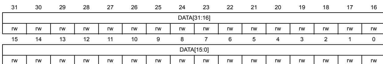
| 31 | 30 | 29 | 28 | 27 | 26 | 25 | 24 | 23 | 22 | 21 | 20 | 19 | 18 | 17 | 16 |
| DATA[31:16] | |||||||||||||||
| rw | rw | rw | rw | rw | rw | rw | rw | rw | rw | rw | rw | rw | rw | rw | rw |
| 15 | 14 | 13 | 12 | 11 | 10 | 9 | 8 | 7 | 6 | 5 | 4 | 3 | 2 | 1 | 0 |
| DATA[15:0] | |||||||||||||||
| rw | rw | rw | rw | rw | rw | rw | rw | rw | rw | rw | rw | rw | rw | rw | rw |
Bits 31:0 DATA[31:0] : Data
Data to be sent/received to/from the external SPI device
In indirect-write mode, data written to this register is stored on the FIFO before it is sent to the external device during the data phase. If the FIFO is too full, a write operation is stalled until the FIFO has enough space to accept the amount of data being written.
In indirect-read mode, reading this register gives (via the FIFO) the data that was received from the external device. If the FIFO does not have as many bytes as requested by the read operation and if BUSY = 1, the read operation is stalled until enough data is present or until the transfer is complete, whichever happens first.
In automatic status-polling mode, this register contains the last data read from the external device (without masking).
Word, half-word, and byte accesses to this register are supported. In indirect-write mode, a byte write adds 1 byte to the FIFO, a half-word write 2 bytes, and a word write 4 bytes.
Similarly, in indirect-read mode, a byte read removes 1 byte from the FIFO, a half-word read 2 bytes, and a word read 4 bytes. Accesses in indirect mode must be aligned to the bottom of this register: A byte read must read DATA[7:0] and a half-word read must read DATA[15:0].
24.7.11 XSPI polling status mask register (XSPI_PSMKR)
Address offset: 0x080
Reset value: 0x0000 0000
This register can be modified only when BUSY = 0.
| 31 | 30 | 29 | 28 | 27 | 26 | 25 | 24 | 23 | 22 | 21 | 20 | 19 | 18 | 17 | 16 |
|---|---|---|---|---|---|---|---|---|---|---|---|---|---|---|---|
| MASK[31:16] | |||||||||||||||
| rw | rw | rw | rw | rw | rw | rw | rw | rw | rw | rw | rw | rw | rw | rw | rw |
| 15 | 14 | 13 | 12 | 11 | 10 | 9 | 8 | 7 | 6 | 5 | 4 | 3 | 2 | 1 | 0 |
| MASK[15:0] | |||||||||||||||
| rw | rw | rw | rw | rw | rw | rw | rw | rw | rw | rw | rw | rw | rw | rw | rw |
Bits 31:0 MASK[31:0] : Status mask
Mask to be applied to the status bytes received in automatic status-polling mode
For bit n:
0: Bit n of the data received in automatic status-polling mode is masked and its value is not considered in the matching logic.
1: Bit n of the data received in automatic status-polling mode is unmasked and its value is considered in the matching logic.
24.7.12 XSPI polling status match register (XSPI_PSMAR)
Address offset: 0x088
Reset value: 0x0000 0000
This register can be modified only when BUSY = 0.
| 31 | 30 | 29 | 28 | 27 | 26 | 25 | 24 | 23 | 22 | 21 | 20 | 19 | 18 | 17 | 16 |
|---|---|---|---|---|---|---|---|---|---|---|---|---|---|---|---|
| MATCH[31:16] | |||||||||||||||
| rw | rw | rw | rw | rw | rw | rw | rw | rw | rw | rw | rw | rw | rw | rw | rw |
| 15 | 14 | 13 | 12 | 11 | 10 | 9 | 8 | 7 | 6 | 5 | 4 | 3 | 2 | 1 | 0 |
| MATCH[15:0] | |||||||||||||||
| rw | rw | rw | rw | rw | rw | rw | rw | rw | rw | rw | rw | rw | rw | rw | rw |
Bits 31:0 MATCH[31:0] : Status match
Value to be compared with the masked status register to get a match
24.7.13 XSPI polling interval register (XSPI_PIR)
Address offset: 0x090
Reset value: 0x0000 0000
This register can be modified only when BUSY = 0.
| 31 | 30 | 29 | 28 | 27 | 26 | 25 | 24 | 23 | 22 | 21 | 20 | 19 | 18 | 17 | 16 |
|---|---|---|---|---|---|---|---|---|---|---|---|---|---|---|---|
| Res. | Res. | Res. | Res. | Res. | Res. | Res. | Res. | Res. | Res. | Res. | Res. | Res. | Res. | Res. | Res. |
| 15 | 14 | 13 | 12 | 11 | 10 | 9 | 8 | 7 | 6 | 5 | 4 | 3 | 2 | 1 | 0 |
| INTERVAL[15:0] | |||||||||||||||
| rw | rw | rw | rw | rw | rw | rw | rw | rw | rw | rw | rw | rw | rw | rw | rw |
Bits 31:16 Reserved, must be kept at reset value.
Bits 15:0 INTERVAL[15:0] : Polling interval
Number of CLK cycles between a read during the automatic status-polling phases
24.7.14 XSPI communication configuration register (XSPI_CCR)
Address offset: 0x100
Reset value: 0x0000 0000
This register can be modified only when BUSY = 0.
| 31 | 30 | 29 | 28 | 27 | 26 | 25 | 24 | 23 | 22 | 21 | 20 | 19 | 18 | 17 | 16 |
|---|---|---|---|---|---|---|---|---|---|---|---|---|---|---|---|
| Res. | Res. | DQSE | Res. | DDTR | DMODE[2:0] | Res. | Res. | ABSIZE[1:0] | ABDTR | ABMODE[2:0] | |||||
| rw | rw | rw | rw | rw | rw | rw | rw | rw | rw | rw | |||||
| 15 | 14 | 13 | 12 | 11 | 10 | 9 | 8 | 7 | 6 | 5 | 4 | 3 | 2 | 1 | 0 |
| Res. | Res. | ADSIZE[1:0] | ADDTR | ADMODE[2:0] | Res. | Res. | ISIZE[1:0] | IDTR | IMODE[2:0] | ||||||
| rw | rw | rw | rw | rw | rw | rw | rw | rw | rw | rw | rw | ||||
Bits 31:30 Reserved, must be kept at reset value.
Bit 29 DQSE : DQS enable
This bit enables the data strobe management.
0: DQS disabled
1: DQS enabled
Bit 28 Reserved, must be kept at reset value.
Bit 27 DDTR : Data double transfer rate
This bit sets the DTR mode for the data phase.
0: DTR mode disabled for the data phase
1: DTR mode enabled for the data phase
Bits 26:24 DMODE[2:0] : Data mode
This bitfield defines the data phase mode of operation.
000: No data
001: Data on a single line
010: Data on two lines
011: Data on four lines
100: Data on eight lines
101: Data on 16 lines
Others: Reserved
Bits 23:22 Reserved, must be kept at reset value.
Bits 21:20 ABSIZE[1:0] : Alternate-byte size
This bitfield defines the alternate-byte size.
00: 8-bit alternate bytes
01: 16-bit alternate bytes
10: 24-bit alternate bytes
11: 32-bit alternate bytes
Bit 19 ABDTR : Alternate-byte double transfer rate
This bit sets the DTR mode for the alternate-byte phase.
0: DTR mode disabled for the alternate-byte phase
1: DTR mode enabled for the alternate-byte phase
Bits 18:16 ABMODE[2:0] : Alternate-byte mode
This bitfield defines the alternate-byte phase mode of operation.
000: No alternate bytes
001: Alternate bytes on a single line
010: Alternate bytes on two lines
011: Alternate bytes on four lines
100: Alternate bytes on eight lines
Others: Reserved
Bits 15:14 Reserved, must be kept at reset value.
Bits 13:12 ADSIZE[1:0] : Address size
This bitfield defines the address size.
00: 8-bit address
01: 16-bit address
10: 24-bit address
11: 32-bit address
Bit 11 ADDTR : Address double transfer rate
This bit sets the DTR mode for the address phase.
0: DTR mode disabled for the address phase
1: DTR mode enabled for the address phase
Bits 10:8 ADMODE[2:0] : Address mode
This bitfield defines the address phase mode of operation.
000: No address
001: Address on a single line
010: Address on two lines
011: Address on four lines
100: Address on eight lines
Others: Reserved
Bits 7:6 Reserved, must be kept at reset value.
Bits 5:4 ISIZE[1:0] : Instruction size
This bitfield defines the instruction size.
00: 8-bit instruction
01: 16-bit instruction
10: 24-bit instruction
11: 32-bit instruction
Bit 3 IDTR : Instruction double transfer rate
This bit sets the DTR mode for the instruction phase.
0: DTR mode disabled for the instruction phase
1: DTR mode enabled for the instruction phase
Bits 2:0 IMODE[2:0] : Instruction mode
This bitfield defines the instruction phase mode of operation.
000: No instruction
001: Instruction on a single line
010: Instruction on two lines
011: Instruction on four lines
100: Instruction on eight lines
Others: Reserved
24.7.15 XSPI timing configuration register (XSPI_TCR)
Address offset: 0x108
Reset value: 0x0000 0000
This register can be modified only when BUSY = 0.
| 31 | 30 | 29 | 28 | 27 | 26 | 25 | 24 | 23 | 22 | 21 | 20 | 19 | 18 | 17 | 16 |
|---|---|---|---|---|---|---|---|---|---|---|---|---|---|---|---|
| Res. | SSHIFT | Res. | Res. | Res. | Res. | Res. | Res. | Res. | Res. | Res. | Res. | Res. | Res. | Res. | Res. |
| rw | |||||||||||||||
| 15 | 14 | 13 | 12 | 11 | 10 | 9 | 8 | 7 | 6 | 5 | 4 | 3 | 2 | 1 | 0 |
| Res. | Res. | Res. | Res. | Res. | Res. | Res. | Res. | Res. | Res. | Res. | DCYC[4:0] | ||||
| rw | rw | rw | rw | rw | |||||||||||
Bit 31 Reserved, must be kept at reset value.
Bit 30 SSHIFT : Sample shift
By default, the XSPI samples data 1/2 of a CLK cycle after the data is driven by the external device.
This bit allows the data to be sampled later in order to consider the external signal delays.
0: No shift
1: 1/2 cycle shift
The software must ensure that SSHIFT = 0 when the data phase is configured in DTR mode (when DDTR = 1.)
Bits 29:5 Reserved, must be kept at reset value.
Bits 4:0 DCYC[4:0] : Number of dummy cycles
This bitfield defines the duration of the dummy phase according to the memory latency.
In both SDR and DTR modes, it specifies a number of CLK cycles (0-31).
24.7.16 XSPI instruction register (XSPI_IR)
Address offset: 0x110
Reset value: 0x0000 0000
This register can be modified only when BUSY = 0.
| 31 | 30 | 29 | 28 | 27 | 26 | 25 | 24 | 23 | 22 | 21 | 20 | 19 | 18 | 17 | 16 |
| INSTRUCTION[31:16] | |||||||||||||||
| rw | rw | rw | rw | rw | rw | rw | rw | rw | rw | rw | rw | rw | rw | rw | rw |
| 15 | 14 | 13 | 12 | 11 | 10 | 9 | 8 | 7 | 6 | 5 | 4 | 3 | 2 | 1 | 0 |
| INSTRUCTION[15:0] | |||||||||||||||
| rw | rw | rw | rw | rw | rw | rw | rw | rw | rw | rw | rw | rw | rw | rw | rw |
Bits 31:0
INSTRUCTION[31:0]
: Instruction
Instruction to be sent to the external SPI device
24.7.17 XSPI alternate bytes register (XSPI_ABR)
Address offset: 0x120
Reset value: 0x0000 0000
This register can be modified only when BUSY = 0.
| 31 | 30 | 29 | 28 | 27 | 26 | 25 | 24 | 23 | 22 | 21 | 20 | 19 | 18 | 17 | 16 |
| ALTERNATE[31:16] | |||||||||||||||
| rw | rw | rw | rw | rw | rw | rw | rw | rw | rw | rw | rw | rw | rw | rw | rw |
| 15 | 14 | 13 | 12 | 11 | 10 | 9 | 8 | 7 | 6 | 5 | 4 | 3 | 2 | 1 | 0 |
| ALTERNATE[15:0] | |||||||||||||||
| rw | rw | rw | rw | rw | rw | rw | rw | rw | rw | rw | rw | rw | rw | rw | rw |
Bits 31:0
ALTERNATE[31:0]
: Alternate bytes
Optional data to be sent to the external SPI device right after the address.
24.7.18 XSPI low-power timeout register (XSPI_LPTR)
Address offset: 0x130
Reset value: 0x0000 0000
This register can be modified only when BUSY = 0.
| 31 | 30 | 29 | 28 | 27 | 26 | 25 | 24 | 23 | 22 | 21 | 20 | 19 | 18 | 17 | 16 |
| Res. | Res. | Res. | Res. | Res. | Res. | Res. | Res. | Res. | Res. | Res. | Res. | Res. | Res. | Res. | Res. |
| 15 | 14 | 13 | 12 | 11 | 10 | 9 | 8 | 7 | 6 | 5 | 4 | 3 | 2 | 1 | 0 |
| TIMEOUT[15:0] | |||||||||||||||
| rw | rw | rw | rw | rw | rw | rw | rw | rw | rw | rw | rw | rw | rw | rw | rw |
Bits 31:16 Reserved, must be kept at reset value.
Bits 15:0 TIMEOUT[15:0] : Timeout period
After each access in memory-mapped mode, the XSPI prefetches the subsequent bytes and hold them in the FIFO.
This bitfield indicates how many CLK cycles the XSPI waits after the clock becomes inactive and until it raises the NCS, putting the external device in a lower-consumption state.
24.7.19 XSPI wrap communication configuration register (XSPI_WPCCR)
Address offset: 0x140
Reset value: 0x0000 0000
This register can be modified only when BUSY = 0.
| 31 | 30 | 29 | 28 | 27 | 26 | 25 | 24 | 23 | 22 | 21 | 20 | 19 | 18 | 17 | 16 |
|---|---|---|---|---|---|---|---|---|---|---|---|---|---|---|---|
| Res. | Res. | DQSE | Res. | DDTR | DMODE[2:0] | Res. | Res. | ABSIZE[1:0] | ABDTR | ABMODE[2:0] | |||||
| rw | rw | rw | rw | rw | rw | rw | rw | rw | rw | rw | |||||
| 15 | 14 | 13 | 12 | 11 | 10 | 9 | 8 | 7 | 6 | 5 | 4 | 3 | 2 | 1 | 0 |
|---|---|---|---|---|---|---|---|---|---|---|---|---|---|---|---|
| Res. | Res. | ADSIZE[1:0] | ADDTR | ADMODE[2:0] | Res. | Res. | ISIZE[1:0] | IDTR | IMODE[2:0] | ||||||
| rw | rw | rw | rw | rw | rw | rw | rw | rw | rw | rw | rw | ||||
Bits 31:30 Reserved, must be kept at reset value.
Bit 29 DQSE : DQS enable
This bit enables the data strobe management.
0: DQS disabled
1: DQS enabled
Bit 28 Reserved, must be kept at reset value.
Bit 27 DDTR : Data double transfer rate
This bit sets the DTR mode for the data phase.
0: DTR mode disabled for the data phase
1: DTR mode enabled for the data phase
Bits 26:24 DMODE[2:0] : Data mode
This bitfield defines the data phase mode of operation.
000: No data
001: Data on a single line
010: Data on two lines
011: Data on four lines
100: Data on eight lines
101: Data on 16 lines
Others: Reserved
Bits 23:22 Reserved, must be kept at reset value.
Bits 21:20 ABSIZE[1:0] : Alternate-byte size
This bitfield defines the alternate-byte size.
00: 8-bit alternate bytes
01: 16-bit alternate bytes
10: 24-bit alternate bytes
11: 32-bit alternate bytes
Bit 19 ABDTR : Alternate-byte double transfer rate
This bit sets the DTR mode for the alternate-byte phase.
0: DTR mode disabled for the alternate-byte phase
1: DTR mode enabled for the alternate-byte phase
Bits 18:16 ABMODE[2:0] : Alternate-byte mode
This bitfield defines the alternate byte phase mode of operation.
000: No alternate bytes
001: Alternate bytes on a single line
010: Alternate bytes on two lines
011: Alternate bytes on four lines
100: Alternate bytes on eight lines
Others: Reserved
Bits 15:14 Reserved, must be kept at reset value.
Bits 13:12 ADSIZE[1:0] : Address size
This bitfield defines the address size.
00: 8-bit address
01: 16-bit address
10: 24-bit address
11: 32-bit address
Bit 11 ADDTR : Address double transfer rate
This bit sets the DTR mode for the address phase.
0: DTR mode disabled for the address phase
1: DTR mode enabled for the address phase
Bits 10:8 ADMODE[2:0] : Address mode
This bitfield defines the address phase mode of operation.
000: No address
001: Address on a single line
010: Address on two lines
011: Address on four lines
100: Address on eight lines
Others: Reserved
Bits 7:6 Reserved, must be kept at reset value.
Bits 5:4 ISIZE[1:0] : Instruction size
This bitfield defines the instruction size.
00: 8-bit instruction
01: 16-bit instruction
10: 24-bit instruction
11: 32-bit instruction
Bit 3 IDTR : Instruction double transfer rate
This bit sets the DTR mode for the instruction phase.
0: DTR mode disabled for the instruction phase
1: DTR mode enabled for the instruction phase
Bits 2:0 IMODE[2:0] : Instruction mode
This bitfield defines the instruction phase mode of operation.
000: No instruction
001: Instruction on a single line
010: Instruction on two lines
011: Instruction on four lines
100: Instruction on eight lines
Others: Reserved
24.7.20 XSPI wrap timing configuration register (XSPI_WPTCR)
Address offset: 0x148
Reset value: 0x0000 0000
This register can be modified only when BUSY = 0.
| 31 | 30 | 29 | 28 | 27 | 26 | 25 | 24 | 23 | 22 | 21 | 20 | 19 | 18 | 17 | 16 |
|---|---|---|---|---|---|---|---|---|---|---|---|---|---|---|---|
| Res. | SSHIFT | Res. | Res. | Res. | Res. | Res. | Res. | Res. | Res. | Res. | Res. | Res. | Res. | Res. | Res. |
| rw | |||||||||||||||
| 15 | 14 | 13 | 12 | 11 | 10 | 9 | 8 | 7 | 6 | 5 | 4 | 3 | 2 | 1 | 0 |
| Res. | Res. | Res. | Res. | Res. | Res. | Res. | Res. | Res. | Res. | Res. | DCYC[4:0] | ||||
| rw | rw | rw | rw | rw | |||||||||||
Bit 31 Reserved, must be kept at reset value.
Bit 30 SSHIFT : Sample shift
By default, the XSPI samples data 1/2 of a CLK cycle after the data is driven by the external device.
This bit allows the data to be sampled later in order to consider the external signal delays.
0: No shift
1: 1/2 cycle shift
The software must ensure that SSHIFT = 0 when the data phase is configured in DTR mode (when DDTR = 1).
Bits 29:5 Reserved, must be kept at reset value.
Bits 4:0 DCYC[4:0] : Number of dummy cycles
This bitfield defines the duration of the dummy phase according to the memory latency.
In both SDR and DTR modes, it specifies a number of CLK cycles (0-31).
24.7.21 XSPI wrap instruction register (XSPI_WPIR)
Address offset: 0x150
Reset value: 0x0000 0000
This register can be modified only when BUSY = 0.
| 31 | 30 | 29 | 28 | 27 | 26 | 25 | 24 | 23 | 22 | 21 | 20 | 19 | 18 | 17 | 16 |
|---|---|---|---|---|---|---|---|---|---|---|---|---|---|---|---|
| INSTRUCTION[31:16] | |||||||||||||||
| rw | rw | rw | rw | rw | rw | rw | rw | rw | rw | rw | rw | rw | rw | rw | rw |
| 15 | 14 | 13 | 12 | 11 | 10 | 9 | 8 | 7 | 6 | 5 | 4 | 3 | 2 | 1 | 0 |
| INSTRUCTION[15:0] | |||||||||||||||
| rw | rw | rw | rw | rw | rw | rw | rw | rw | rw | rw | rw | rw | rw | rw | rw |
Bits 31:0
INSTRUCTION[31:0]
: Instruction
Instruction to be sent to the external SPI device
24.7.22 XSPI wrap alternate byte register (XSPI_WPABR)
Address offset: 0x160
Reset value: 0x0000 0000
This register can be modified only when BUSY = 0.
| 31 | 30 | 29 | 28 | 27 | 26 | 25 | 24 | 23 | 22 | 21 | 20 | 19 | 18 | 17 | 16 |
|---|---|---|---|---|---|---|---|---|---|---|---|---|---|---|---|
| ALTERNATE[31:16] | |||||||||||||||
| rw | rw | rw | rw | rw | rw | rw | rw | rw | rw | rw | rw | rw | rw | rw | rw |
| 15 | 14 | 13 | 12 | 11 | 10 | 9 | 8 | 7 | 6 | 5 | 4 | 3 | 2 | 1 | 0 |
| ALTERNATE[15:0] | |||||||||||||||
| rw | rw | rw | rw | rw | rw | rw | rw | rw | rw | rw | rw | rw | rw | rw | rw |
Bits 31:0
ALTERNATE[31:0]
: Alternate bytes
Optional data to be sent to the external SPI device right after the address
24.7.23 XSPI write communication configuration register (XSPI_WCCR)
Address offset: 0x180
Reset value: 0x0000 0000
This register can be modified only when BUSY = 0. Its content has a meaning only when requesting write operations in memory-mapped mode.
| 31 | 30 | 29 | 28 | 27 | 26 | 25 | 24 | 23 | 22 | 21 | 20 | 19 | 18 | 17 | 16 |
|---|---|---|---|---|---|---|---|---|---|---|---|---|---|---|---|
| Res. | Res. | DQSE | Res. | DDTR | DMODE[2:0] | Res. | Res. | ABSIZE[1:0] | ABDTR | ABMODE[2:0] | |||||
| rw | rw | rw | rw | rw | rw | rw | rw | rw | rw | rw | |||||
| 15 | 14 | 13 | 12 | 11 | 10 | 9 | 8 | 7 | 6 | 5 | 4 | 3 | 2 | 1 | 0 |
| Res. | Res. | ADSIZE[1:0] | ADDTR | ADMODE[2:0] | Res. | Res. | ISIZE[1:0] | IDTR | IMODE[2:0] | ||||||
| rw | rw | rw | rw | rw | rw | rw | rw | rw | rw | rw | rw | ||||
Bits 31:30 Reserved, must be kept at reset value.
Bit 29 DQSE : DQS enable
This bit enables the data strobe management.
0: DQS disabled
1: DQS enabled
Bit 28 Reserved, must be kept at reset value.
Bit 27 DDTR : Data double transfer rate
This bit sets the DTR mode for the data phase.
0: DTR mode disabled for the data phase
1: DTR mode enabled for the data phase
Bits 26:24 DMODE[2:0] : Data mode
This bitfield defines the data phase mode of operation.
000: No data
001: Data on a single line
010: Data on two lines
011: Data on four lines
100: Data on eight lines
101: Data on 16 lines
Others: Reserved
Bits 23:22 Reserved, must be kept at reset value.
Bits 21:20 ABSIZE[1:0] : Alternate-byte size
This bitfield defines the alternate-byte size:
00: 8-bit alternate bytes
01: 16-bit alternate bytes
10: 24-bit alternate bytes
11: 32-bit alternate bytes
Bit 19 ABDTR : Alternate-byte double-transfer rate
This bit sets the DTR mode for the alternate-byte phase.
0: DTR mode disabled for the alternate-byte phase
1: DTR mode enabled for the alternate-byte phase
Bits 18:16 ABMODE[2:0] : Alternate-byte mode
This bitfield defines the alternate-byte phase mode of operation.
000: No alternate bytes
001: Alternate bytes on a single line
010: Alternate bytes on two lines
011: Alternate bytes on four lines
100: Alternate bytes on eight lines
Others: Reserved
Bits 15:14 Reserved, must be kept at reset value.
Bits 13:12 ADSIZE[1:0] : Address size
This bitfield defines the address size.
00: 8-bit address
01: 16-bit address
10: 24-bit address
11: 32-bit address
Bit 11
ADDTR
: Address double transfer rate
This bit sets the DTR mode for the address phase.
0: DTR mode disabled for the address phase
1: DTR mode enabled for the address phase
Bits 10:8
ADMODE[2:0]
: Address mode
This bitfield defines the address phase mode of operation.
000: No address
001: Address on a single line
010: Address on two lines
011: Address on four lines
100: Address on eight lines
Others: Reserved
Bits 7:6 Reserved, must be kept at reset value.
Bits 5:4
ISIZE[1:0]
: Instruction size
This bitfield defines the instruction size:
00: 8-bit instruction
01: 16-bit instruction
10: 24-bit instruction
11: 32-bit instruction
Bit 3
IDTR
: Instruction double transfer rate
This bit sets the DTR mode for the instruction phase.
0: DTR mode disabled for the instruction phase
1: DTR mode enabled for the instruction phase
Bits 2:0
IMODE[2:0]
: Instruction mode
This bitfield defines the instruction phase mode of operation.
000: No instruction
001: Instruction on a single line
010: Instruction on two lines
011: Instruction on four lines
100: Instruction on eight lines
Others: Reserved
24.7.24 XSPI write timing configuration register (XSPI_WTCR)
Address offset: 0x188
Reset value: 0x0000 0000
This register can be modified only when BUSY = 0. Its content has a meaning only when requesting write operations in memory-mapped mode.
| 31 | 30 | 29 | 28 | 27 | 26 | 25 | 24 | 23 | 22 | 21 | 20 | 19 | 18 | 17 | 16 |
|---|---|---|---|---|---|---|---|---|---|---|---|---|---|---|---|
| Res. | Res. | Res. | Res. | Res. | Res. | Res. | Res. | Res. | Res. | Res. | Res. | Res. | Res. | Res. | Res. |
| 15 | 14 | 13 | 12 | 11 | 10 | 9 | 8 | 7 | 6 | 5 | 4 | 3 | 2 | 1 | 0 |
| Res. | Res. | Res. | Res. | Res. | Res. | Res. | Res. | Res. | Res. | Res. | DCYC[4:0] | ||||
| rw | rw | rw | rw | rw | |||||||||||
Bits 31:5 Reserved, must be kept at reset value.
Bits 4:0 DCYC[4:0] : Number of dummy cycles
This bitfield defines the duration of the dummy phase according to the memory latency.
In both SDR and DTR modes, it specifies a number of CLK cycles (0-31).
24.7.25 XSPI write instruction register (XSPI_WIR)
Address offset: 0x190
Reset value: 0x0000 0000
This register can be modified only when BUSY = 0. Its content has a meaning only when requesting write operations in memory-mapped mode.
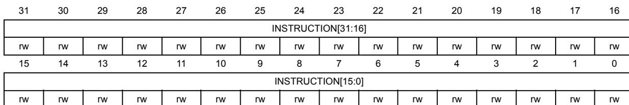
| 31 | 30 | 29 | 28 | 27 | 26 | 25 | 24 | 23 | 22 | 21 | 20 | 19 | 18 | 17 | 16 |
| INSTRUCTION[31:16] | |||||||||||||||
| rw | rw | rw | rw | rw | rw | rw | rw | rw | rw | rw | rw | rw | rw | rw | rw |
| 15 | 14 | 13 | 12 | 11 | 10 | 9 | 8 | 7 | 6 | 5 | 4 | 3 | 2 | 1 | 0 |
| INSTRUCTION[15:0] | |||||||||||||||
| rw | rw | rw | rw | rw | rw | rw | rw | rw | rw | rw | rw | rw | rw | rw | rw |
Bits 31:0 INSTRUCTION[31:0] : Instruction
Instruction to be sent to the external SPI device
24.7.26 XSPI write alternate byte register (XSPI_WABR)
Address offset: 0x1A0
Reset value: 0x0000 0000
This register can be modified only when BUSY = 0. Its content has a meaning only when requesting write operations in memory-mapped mode.
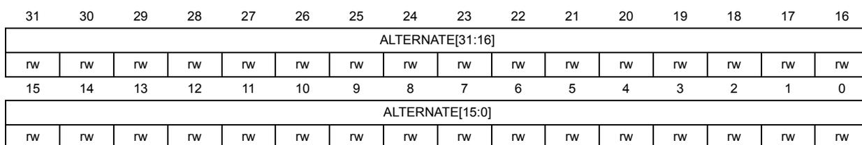
| 31 | 30 | 29 | 28 | 27 | 26 | 25 | 24 | 23 | 22 | 21 | 20 | 19 | 18 | 17 | 16 |
| ALTERNATE[31:16] | |||||||||||||||
| rw | rw | rw | rw | rw | rw | rw | rw | rw | rw | rw | rw | rw | rw | rw | rw |
| 15 | 14 | 13 | 12 | 11 | 10 | 9 | 8 | 7 | 6 | 5 | 4 | 3 | 2 | 1 | 0 |
| ALTERNATE[15:0] | |||||||||||||||
| rw | rw | rw | rw | rw | rw | rw | rw | rw | rw | rw | rw | rw | rw | rw | rw |
Bits 31:0 ALTERNATE[31:0] : Alternate bytes
Optional data to be sent to the external SPI device right after the address
24.7.27 XSPI HyperBus latency configuration register (XSPI_HLCR)
Address offset: 0x200
Reset value: 0x0000 0000
This register can be modified only when BUSY = 0.
| 31 | 30 | 29 | 28 | 27 | 26 | 25 | 24 | 23 | 22 | 21 | 20 | 19 | 18 | 17 | 16 |
|---|---|---|---|---|---|---|---|---|---|---|---|---|---|---|---|
| Res. | Res. | Res. | Res. | Res. | Res. | Res. | Res. | TRWR[7:0] | |||||||
| rw | rw | rw | rw | rw | rw | rw | rw | ||||||||
| 15 | 14 | 13 | 12 | 11 | 10 | 9 | 8 | 7 | 6 | 5 | 4 | 3 | 2 | 1 | 0 |
| TACC[7:0] | Res. | Res. | Res. | Res. | Res. | Res. | WZL | LM | |||||||
| rw | rw | rw | rw | rw | rw | rw | rw | rw | rw | ||||||
Bits 31:24 Reserved, must be kept at reset value.
Bits 23:16 TRWR[7:0] : Read-write minimum recovery time
Device Read-to-write/write-to-read minimum recovery time expressed in number of communication clock cycles
Bits 15:8 TACC[7:0] : Access time
Device access time according to the memory latency, expressed in number of communication clock cycles
Bits 7:2 Reserved, must be kept at reset value.
Bit 1 WZL : Write zero latency
This bit enables zero latency on write operations.
0: Latency on write accesses
1: No latency on write accesses
Bit 0 LM : Latency mode
This bit selects the latency mode.
0: Variable initial latency
1: Fixed latency
Note: This bit must be set when using the dual-octal HyperBus configuration.
24.7.28 XSPI full-cycle calibration configuration (XSPI_CALFCR)
Address offset: 0x210
Reset value: 0x0000 0000
This read-only register gives the calibration code needed by the DLL master so that its delay is equivalent to a full memory-clock cycle. The value of this register is updated every time that auto-calibration finishes.
| 31 | 30 | 29 | 28 | 27 | 26 | 25 | 24 | 23 | 22 | 21 | 20 | 19 | 18 | 17 | 16 |
|---|---|---|---|---|---|---|---|---|---|---|---|---|---|---|---|
| CALMAX | Res. | Res. | Res. | Res. | Res. | Res. | Res. | Res. | Res. | Res. | COARSE[4:0] | ||||
| r | r | r | r | r | r | ||||||||||
| 15 | 14 | 13 | 12 | 11 | 10 | 9 | 8 | 7 | 6 | 5 | 4 | 3 | 2 | 1 | 0 |
| Res. | Res. | Res. | Res. | Res. | Res. | Res. | Res. | Res. | FINE[6:0] | ||||||
| r | r | r | r | r | r | r | |||||||||
Bit 31 CALMAX : Max value
This bit gets set when the memory-clock period is outside the range of DLL master, in which case XSPI_CALFCR and XSPI_CALSR are updated with the values for the maximum delay.
Bits 30:21 Reserved, must be kept at reset value.
Bits 20:16 COARSE[4:0] : Coarse calibration
The delay unitary value for this bitfield depends on product technology (see the datasheet).
Bits 15:7 Reserved, must be kept at reset value.
Bits 6:0 FINE[6:0] : Fine calibration
The delay unitary value for this bitfield depends on product technology (see the datasheet).
24.7.29 XSPI DLL master calibration configuration (XSPI_CALMR)
Address offset: 0x218
Reset value: 0x0000 0000
The DLL Master is used for delaying the feedback clock when reading without DQS.
The delay of the master DLL is determined by the value in this register.
This register can always be read by software and can be modified only when BUSY = 0.
This register never gets updated automatically by hardware.
| 31 | 30 | 29 | 28 | 27 | 26 | 25 | 24 | 23 | 22 | 21 | 20 | 19 | 18 | 17 | 16 |
|---|---|---|---|---|---|---|---|---|---|---|---|---|---|---|---|
| Res. | Res. | Res. | Res. | Res. | Res. | Res. | Res. | Res. | Res. | Res. | COARSE[4:0] | ||||
| rw | rw | rw | rw | rw | |||||||||||
| 15 | 14 | 13 | 12 | 11 | 10 | 9 | 8 | 7 | 6 | 5 | 4 | 3 | 2 | 1 | 0 |
| Res. | Res. | Res. | Res. | Res. | Res. | Res. | Res. | Res. | FINE[6:0] | ||||||
| rw | rw | rw | rw | rw | rw | rw | |||||||||
Bits 31:21 Reserved, must be kept at reset value.
Bits 20:16 COARSE[4:0] : Coarse calibration
The delay unitary value for this bitfield depends on product technology (see the datasheet).
Bits 15:7 Reserved, must be kept at reset value.
Bits 6:0 FINE[6:0] : Fine calibration
The delay unitary value for this bitfield depends on product technology (see the datasheet).
24.7.30 XSPI DLL slave output calibration configuration (XSPI_CALSOR)
Address offset: 0x220
Reset value: 0x0000 0000
The DLL output slave is used to delay the output data in DDR mode for write operations. The delay of the output slave DLL is determined by the value in this register.
This register is updated automatically by hardware at the end of calibration (at the same moment that XSPI_CALFCR is updated).
If this register is written after the last write to XSPI_DCR2 or XSPI_CCR, then auto-calibration is not executed on the next transfer (auto-calibration is not performed for XSPI_CALSIR as well).
This register can always be read by software and can be modified only when BUSY = 0.
| 31 | 30 | 29 | 28 | 27 | 26 | 25 | 24 | 23 | 22 | 21 | 20 | 19 | 18 | 17 | 16 |
|---|---|---|---|---|---|---|---|---|---|---|---|---|---|---|---|
| Res. | Res. | Res. | Res. | Res. | Res. | Res. | Res. | Res. | Res. | Res. | COARSE[4:0] | ||||
| rw | rw | rw | rw | rw | |||||||||||
| 15 | 14 | 13 | 12 | 11 | 10 | 9 | 8 | 7 | 6 | 5 | 4 | 3 | 2 | 1 | 0 |
| Res. | Res. | Res. | Res. | Res. | Res. | Res. | Res. | Res. | FINE[6:0] | ||||||
| rw | rw | rw | rw | rw | rw | rw | |||||||||
Bits 31:21 Reserved, must be kept at reset value.
Bits 20:16 COARSE[4:0] : Coarse calibration
The delay unitary value for this bitfield depends on product technology.
Bits 15:7 Reserved, must be kept at reset value.
Bits 6:0 FINE[6:0] : Fine calibration
The delay unitary value for this bitfield depends on product technology.
24.7.31 XSPI DLL slave input calibration configuration (XSPI_CALSIR)
Address offset: 0x228
Reset value: 0x0000 0000
The DLL input slave is used to delay the DQS input for sampling the data when DQS is enabled for read operations. The delay of the input slave DLL is determined by the value in this register.
This register is updated automatically by hardware at the end of calibration (at the same moment that XSPI_CALFCR is updated).
If this register is written after the last write to XSPI_DCR2 or XSPI_CCR, then auto-calibration is not executed on the next transfer (auto-calibration is not performed for XSPI_CALSOR as well).
This register can always be read by software and can be modified only when BUSY = 0.
| 31 | 30 | 29 | 28 | 27 | 26 | 25 | 24 | 23 | 22 | 21 | 20 | 19 | 18 | 17 | 16 |
|---|---|---|---|---|---|---|---|---|---|---|---|---|---|---|---|
| Res. | Res. | Res. | Res. | Res. | Res. | Res. | Res. | Res. | Res. | Res. | COARSE[4:0] | ||||
| rw | rw | rw | rw | rw | |||||||||||
| 15 | 14 | 13 | 12 | 11 | 10 | 9 | 8 | 7 | 6 | 5 | 4 | 3 | 2 | 1 | 0 |
| Res. | Res. | Res. | Res. | Res. | Res. | Res. | Res. | Res. | FINE[6:0] | ||||||
| rw | rw | rw | rw | rw | rw | rw | |||||||||
Bits 31:21 Reserved, must be kept at reset value.
Bits 20:16 COARSE[4:0] : Coarse calibration
The delay unitary value for this bitfield depends on product technology.
Bits 15:7 Reserved, must be kept at reset value.
Bits 6:0 FINE[6:0] : Fine calibration
The delay unitary value for this bitfield depends on product technology.
24.7.32 XSPI register map
Table 215. XSPI register map and reset values
| Offset | Register name | 31 | 30 | 29 | 28 | 27 | 26 | 25 | 24 | 23 | 22 | 21 | 20 | 19 | 18 | 17 | 16 | 15 | 14 | 13 | 12 | 11 | 10 | 9 | 8 | 7 | 6 | 5 | 4 | 3 | 2 | 1 | 0 |
|---|---|---|---|---|---|---|---|---|---|---|---|---|---|---|---|---|---|---|---|---|---|---|---|---|---|---|---|---|---|---|---|---|---|
| 0x000 | XSPI_CR | MSEL[1:0] | FMDOE[1:0] | Res. | Res. | Res. | Res. | Res. | CSSEL | PMM | APMS | Res. | TOIE | SMIE | FTIE | TCIE | TEIE | Res. | Res. | Res. | FTHRES[4:0] | Res. | DMM | Res. | Res. | TCEN | DMAEN | ABORT | EN | ||||
| Reset value | 0 | 0 | 0 | 0 | 0 | 0 | 0 | 0 | 0 | 0 | 0 | 0 | 0 | 0 | 0 | 0 | 0 | 0 | 0 | 0 | 0 | 0 | |||||||||||
| 0x0004 | Reserved | Reserved | |||||||||||||||||||||||||||||||
| 0x008 | XSPI_DCR1 | Res. | Res. | Res. | Res. | Res. | MTYP[2:0] | Res. | Res. | Res. | Res. | DEVSIZE[4:0] | Res. | Res. | CSHT[5:0] | Res. | Res. | Res. | Res. | Res. | Res. | Res. | FRCK | CKMODE | |||||||||
| Reset value | 0 | 0 | 0 | 0 | 0 | 0 | 0 | 0 | 0 | 0 | 0 | 0 | 0 | 0 | 0 | 0 | 0 | ||||||||||||||||
Table 215. XSPI register map and reset values
| Offset | Register name | 31 | 30 | 29 | 28 | 27 | 26 | 25 | 24 | 23 | 22 | 21 | 20 | 19 | 18 | 17 | 16 | 15 | 14 | 13 | 12 | 11 | 10 | 9 | 8 | 7 | 6 | 5 | 4 | 3 | 2 | 1 | 0 | |
|---|---|---|---|---|---|---|---|---|---|---|---|---|---|---|---|---|---|---|---|---|---|---|---|---|---|---|---|---|---|---|---|---|---|---|
| 0x00C | XSPI_DCR2 | Res | Res | Res | Res | Res | Res | Res | Res | Res | Res | Res | Res | Res | Res | WRAPSIZE[2:0] | PRESCALER[7:0] | |||||||||||||||||
| Reset value | 0 | 0 | 0 | 0 0 0 0 0 0 0 0 | ||||||||||||||||||||||||||||||
| 0x010 | XSPI_DCR3 | Res | Res | Res | Res | Res | Res | Res | Res | Res | Res | Res | Res | Res | Res | CSBOUND[4:0] | MAXTRAN[7:0] | |||||||||||||||||
| Reset value | 0 | 0 | 0 | 0 | 0 | 0 0 0 0 0 0 0 0 | ||||||||||||||||||||||||||||
| 0x014 | XSPI_DCR4 | REFRESH[31:0] | ||||||||||||||||||||||||||||||||
| Reset value | 0 | 0 | 0 | 0 | 0 | 0 | 0 | 0 | 0 | 0 | 0 | 0 | 0 | 0 | 0 | 0 | 0 | 0 | 0 | 0 | 0 | 0 | 0 | 0 | 0 | 0 | 0 | 0 | 0 | 0 | 0 | 0 | ||
| 0x018-0x01C | Reserved | Reserved | ||||||||||||||||||||||||||||||||
| 0x020 | XSPI_SR | Res | Res | Res | Res | Res | Res | Res | Res | Res | Res | Res | Res | Res | Res | Res | Res | Res | Res | Res | FLEVEL[5:0] | TEF | ||||||||||||
| Reset value | 0 | 0 | 0 | 0 | 0 | 0 | 0 | |||||||||||||||||||||||||||
| 0x024 | XSPI_FCR | Res | Res | Res | Res | Res | Res | Res | Res | Res | Res | Res | Res | Res | Res | Res | Res | Res | Res | Res | Res | Res | Res | Res | Res | Res | Res | Res | Res | Res | Res | CTEF | ||
| Reset value | 0 | |||||||||||||||||||||||||||||||||
| 0x028-0x03C | Reserved | Reserved | ||||||||||||||||||||||||||||||||
| 0x040 | XSPI_DLR | DL[31:0] | ||||||||||||||||||||||||||||||||
| Reset value | 0 | 0 | 0 | 0 | 0 | 0 | 0 | 0 | 0 | 0 | 0 | 0 | 0 | 0 | 0 | 0 | 0 | 0 | 0 | 0 | 0 | 0 | 0 | 0 | 0 | 0 | 0 | 0 | 0 | 0 | 0 | |||
| 0x044 | Reserved | Reserved | ||||||||||||||||||||||||||||||||
| 0x048 | XSPI_AR | ADDRESS[31:0] | ||||||||||||||||||||||||||||||||
| Reset value | 0 | 0 | 0 | 0 | 0 | 0 | 0 | 0 | 0 | 0 | 0 | 0 | 0 | 0 | 0 | 0 | 0 | 0 | 0 | 0 | 0 | 0 | 0 | 0 | 0 | 0 | 0 | 0 | 0 | 0 | 0 | |||
| 0x04C | Reserved | Reserved | ||||||||||||||||||||||||||||||||
| 0x050 | XSPI_DR | DATA[31:0] | ||||||||||||||||||||||||||||||||
| Reset value | 0 | 0 | 0 | 0 | 0 | 0 | 0 | 0 | 0 | 0 | 0 | 0 | 0 | 0 | 0 | 0 | 0 | 0 | 0 | 0 | 0 | 0 | 0 | 0 | 0 | 0 | 0 | 0 | 0 | 0 | 0 | |||
| 0x054-0x07C | Reserved | Reserved | ||||||||||||||||||||||||||||||||
| 0x080 | XSPI_PSMKR | MASK[31:0] | ||||||||||||||||||||||||||||||||
| Reset value | 0 | 0 | 0 | 0 | 0 | 0 | 0 | 0 | 0 | 0 | 0 | 0 | 0 | 0 | 0 | 0 | 0 | 0 | 0 | 0 | 0 | 0 | 0 | 0 | 0 | 0 | 0 | 0 | 0 | 0 | 0 | |||
| 0x084 | Reserved | Reserved | ||||||||||||||||||||||||||||||||
| 0x088 | XSPI_PSMAR | MATCH[31:0] | ||||||||||||||||||||||||||||||||
| Reset value | 0 | 0 | 0 | 0 | 0 | 0 | 0 | 0 | 0 | 0 | 0 | 0 | 0 | 0 | 0 | 0 | 0 | 0 | 0 | 0 | 0 | 0 | 0 | 0 | 0 | 0 | 0 | 0 | 0 | 0 | 0 | |||
| 0x08C | Reserved | Reserved | ||||||||||||||||||||||||||||||||
| 0x090 | XSPI_PIR | Res | Res | Res | Res | Res | Res | Res | Res | Res | Res | Res | Res | Res | Res | Res | Res | Res | Res | Res | INTERVAL[15:0] | |||||||||||||
| Reset value | 0 | 0 | 0 | 0 | 0 | 0 | 0 | 0 | 0 | 0 | 0 | 0 | 0 | |||||||||||||||||||||
| 0x094-0x0FC | Reserved | Reserved | ||||||||||||||||||||||||||||||||
Table 215. XSPI register map and reset values
| Offset | Register name | 31 | 30 | 29 | 28 | 27 | 26 | 25 | 24 | 23 | 22 | 21 | 20 | 19 | 18 | 17 | 16 | 15 | 14 | 13 | 12 | 11 | 10 | 9 | 8 | 7 | 6 | 5 | 4 | 3 | 2 | 1 | 0 |
|---|---|---|---|---|---|---|---|---|---|---|---|---|---|---|---|---|---|---|---|---|---|---|---|---|---|---|---|---|---|---|---|---|---|
| 0x100 | XSPI_CCR | Res. | Res. | DQSE | Res. | DDTR | DMODE [2:0] | Res. | ABSIZE [1:0] | ABDTR | ABMODE [2:0] | Res. | Res. | ADSIZE [1:0] | ADDTR | ADMODE [2:0] | Res. | Res. | ISIZE [1:0] | IDTR | IMODE [2:0] | ||||||||||||
| Reset value | 0 | 0 | 0 | 0 | 0 | 0 | 0 | 0 | 0 | 0 | 0 | 0 | 0 | 0 | 0 | 0 | 0 | 0 | 0 | 0 | 0 | 0 | 0 | ||||||||||
| 0x104 | Reserved | Reserved | |||||||||||||||||||||||||||||||
| 0x108 | XSPI_TCR | Res. | SSHIFT | Res. | Res. | Res. | Res. | Res. | Res. | Res. | Res. | Res. | Res. | Res. | Res. | Res. | Res. | Res. | Res. | Res. | Res. | Res. | Res. | Res. | Res. | Res. | Res. | Res. | DCYC[4:0] | ||||
| Reset value | 0 | 0 | 0 | 0 | 0 | 0 | |||||||||||||||||||||||||||
| 0x10C | Reserved | Reserved | |||||||||||||||||||||||||||||||
| 0x110 | XSPI_IR | INSTRUCTION[31:0] | |||||||||||||||||||||||||||||||
| Reset value | 0 | 0 | 0 | 0 | 0 | 0 | 0 | 0 | 0 | 0 | 0 | 0 | 0 | 0 | 0 | 0 | 0 | 0 | 0 | 0 | 0 | 0 | 0 | 0 | 0 | 0 | 0 | 0 | 0 | 0 | 0 | 0 | |
| 0x114-0x11C | Reserved | Reserved | |||||||||||||||||||||||||||||||
| 0x120 | XSPI_ABR | ALTERNATE[31:0] | |||||||||||||||||||||||||||||||
| Reset value | 0 | 0 | 0 | 0 | 0 | 0 | 0 | 0 | 0 | 0 | 0 | 0 | 0 | 0 | 0 | 0 | 0 | 0 | 0 | 0 | 0 | 0 | 0 | 0 | 0 | 0 | 0 | 0 | 0 | 0 | 0 | 0 | |
| 0x124-0x12C | Reserved | Reserved | |||||||||||||||||||||||||||||||
| 0x130 | XSPI_LPTR | Res. | Res. | Res. | Res. | Res. | Res. | Res. | Res. | Res. | Res. | Res. | Res. | Res. | Res. | Res. | Res. | TIMEOUT[15:0] | |||||||||||||||
| Reset value | 0 | 0 | 0 | 0 | 0 | 0 | 0 | 0 | 0 | 0 | 0 | 0 | 0 | 0 | 0 | 0 | |||||||||||||||||
| 0x134-0x13C | Reserved | Reserved | |||||||||||||||||||||||||||||||
| 0x140 | XSPI_WPCCR | Res. | Res. | DQSE | Res. | DDTR | DMODE [2:0] | Res. | ABSIZE [1:0] | ABDTR | ABMODE [2:0] | Res. | Res. | ADSIZE [1:0] | ADDTR | ADMODE [2:0] | Res. | Res. | ISIZE [1:0] | IDTR | IMODE [2:0] | ||||||||||||
| Reset value | 0 | 0 | 0 | 0 | 0 | 0 | 0 | 0 | 0 | 0 | 0 | 0 | 0 | 0 | 0 | 0 | 0 | 0 | 0 | 0 | 0 | 0 | 0 | ||||||||||
| 0x144 | Reserved | Reserved | |||||||||||||||||||||||||||||||
| 0x148 | XSPI_WPTCR | Res. | SSHIFT | Res. | Res. | Res. | Res. | Res. | Res. | Res. | Res. | Res. | Res. | Res. | Res. | Res. | Res. | Res. | Res. | Res. | Res. | Res. | Res. | Res. | Res. | Res. | Res. | Res. | DCYC[4:0] | ||||
| Reset value | 0 | 0 | 0 | 0 | 0 | 0 | |||||||||||||||||||||||||||
| 0x14C | Reserved | Reserved | |||||||||||||||||||||||||||||||
| 0x150 | XSPI_WPIR | INSTRUCTION[31:0] | |||||||||||||||||||||||||||||||
| Reset value | 0 | 0 | 0 | 0 | 0 | 0 | 0 | 0 | 0 | 0 | 0 | 0 | 0 | 0 | 0 | 0 | 0 | 0 | 0 | 0 | 0 | 0 | 0 | 0 | 0 | 0 | 0 | 0 | 0 | 0 | 0 | 0 | |
| 0x154-0x15C | Reserved | Reserved | |||||||||||||||||||||||||||||||
| 0x160 | XSPI_WPABR | ALTERNATE[31:0] | |||||||||||||||||||||||||||||||
| Reset value | 0 | 0 | 0 | 0 | 0 | 0 | 0 | 0 | 0 | 0 | 0 | 0 | 0 | 0 | 0 | 0 | 0 | 0 | 0 | 0 | 0 | 0 | 0 | 0 | 0 | 0 | 0 | 0 | 0 | 0 | 0 | 0 | |
| 0x164-0x17C | Reserved | Reserved | |||||||||||||||||||||||||||||||
| 0x180 | XSPI_WCCR | Res. | Res. | DQSE | Res. | DDTR | DMODE [2:0] | Res. | ABSIZE [1:0] | ABDTR | ABMODE [2:0] | Res. | Res. | ADSIZE [1:0] | ADDTR | ADMODE [2:0] | Res. | Res. | ISIZE [1:0] | IDTR | IMODE [2:0] | ||||||||||||
| Reset value | 0 | 0 | 0 | 0 | 0 | 0 | 0 | 0 | 0 | 0 | 0 | 0 | 0 | 0 | 0 | 0 | 0 | 0 | 0 | 0 | 0 | 0 | 0 | ||||||||||
Table 215. XSPI register map and reset values
| Offset | Register name | 31 | 30 | 29 | 28 | 27 | 26 | 25 | 24 | 23 | 22 | 21 | 20 | 19 | 18 | 17 | 16 | 15 | 14 | 13 | 12 | 11 | 10 | 9 | 8 | 7 | 6 | 5 | 4 | 3 | 2 | 1 | 0 |
|---|---|---|---|---|---|---|---|---|---|---|---|---|---|---|---|---|---|---|---|---|---|---|---|---|---|---|---|---|---|---|---|---|---|
| 0x184 | Reserved | Reserved | |||||||||||||||||||||||||||||||
| 0x188 | XSPI_WTCR | Res | Res | Res | Res | Res | Res | Res | Res | Res | Res | Res | Res | Res | Res | Res | Res | Res | Res | Res | Res | Res | Res | Res | Res | Res | Res | Res | Res | Res | Res | DCYC[4:0] | |
| Reset value | 0 | 0 | 0 | 0 | |||||||||||||||||||||||||||||
| 0x18C | Reserved | Reserved | |||||||||||||||||||||||||||||||
| 0x190 | XSPI_WIR | INSTRUCTION[31:0] | |||||||||||||||||||||||||||||||
| Reset value | 0 | 0 | 0 | 0 | 0 | 0 | 0 | 0 | 0 | 0 | 0 | 0 | 0 | 0 | 0 | 0 | 0 | 0 | 0 | 0 | 0 | 0 | 0 | 0 | 0 | 0 | 0 | 0 | 0 | 0 | 0 | 0 | |
| 0x194-0x19C | Reserved | Reserved | |||||||||||||||||||||||||||||||
| 0x1A0 | XSPI_WABR | ALTERNATE[31:0] | |||||||||||||||||||||||||||||||
| Reset value | 0 | 0 | 0 | 0 | 0 | 0 | 0 | 0 | 0 | 0 | 0 | 0 | 0 | 0 | 0 | 0 | 0 | 0 | 0 | 0 | 0 | 0 | 0 | 0 | 0 | 0 | 0 | 0 | 0 | 0 | 0 | 0 | |
| 0x1A4-0x1FC | Reserved | Reserved | |||||||||||||||||||||||||||||||
| 0x200 | XSPI_HLCR | Res | Res | Res | Res | Res | Res | Res | Res | Res | Res | TRWR[7:0] | TACC[7:0] | Res | Res | Res | Res | Res | Res | Res | Res | Res | Res | WZL | LM | ||||||||
| Reset value | 0 | 0 | 0 | 0 | 0 | 0 | 0 | 0 | 0 | 0 | 0 | 0 | |||||||||||||||||||||
| 0x204-0x20C | Reserved | Reserved | |||||||||||||||||||||||||||||||
| 0x210 | XSPI_CALFCR | CALMAX | Res | Res | Res | Res | Res | Res | Res | Res | Res | Res | Res | COARSE[4:0] | Res | Res | Res | Res | Res | Res | Res | Res | Res | Res | Res | Res | Res | Res | Res | FINE[6:0] | |||
| Reset value | 0 | 0 | 0 | 0 | 0 | 0 | 0 | 0 | 0 | ||||||||||||||||||||||||
| 0x214 | Reserved | Reserved | |||||||||||||||||||||||||||||||
| 0x218 | XSPI_CALMR | Res | Res | Res | Res | Res | Res | Res | Res | Res | Res | Res | Res | COARSE[4:0] | Res | Res | Res | Res | Res | Res | Res | Res | Res | Res | Res | Res | Res | Res | Res | FINE[6:0] | |||
| Reset value | 0 | 0 | 0 | 0 | 0 | 0 | 0 | ||||||||||||||||||||||||||
| 0x22C | Reserved | Reserved | |||||||||||||||||||||||||||||||
| 0x220 | XSPI_CALSOR | Res | Res | Res | Res | Res | Res | Res | Res | Res | Res | Res | Res | COARSE[4:0] | Res | Res | Res | Res | Res | Res | Res | Res | Res | Res | Res | Res | Res | Res | Res | FINE[6:0] | |||
| Reset value | 0 | 0 | 0 | 0 | 0 | 0 | 0 | ||||||||||||||||||||||||||
| 0x224 | Reserved | Reserved | |||||||||||||||||||||||||||||||
| 0x228 | XSPI_CALSIR | Res | Res | Res | Res | Res | Res | Res | Res | Res | Res | Res | Res | COARSE[4:0] | Res | Res | Res | Res | Res | Res | Res | Res | Res | Res | Res | Res | Res | Res | Res | FINE[6:0] | |||
| Reset value | 0 | 0 | 0 | 0 | 0 | 0 | 0 | ||||||||||||||||||||||||||
Refer to Section 2.3: Memory organization for the register boundary addresses.