20. Extended interrupt and event controller (EXTI)
The extended interrupt and event controller (EXTI) manages wake-up through configurable and direct event inputs. It provides wake-up requests to the power control, and generates interrupt requests to the CPU NVIC and events to the CPU event input.
The EXTI wake-up requests allow the system to be woken up from Stop mode, and the CPU to be woken up from CStop mode.
Both the interrupt request and event request generation can also be used in Run modes.
20.1 EXTI main features
The EXTI main features are as follows:
- • All event inputs allow the CPU to wake up and to generate a CPU interrupt and/or CPU event
The asynchronous event inputs are classified in 2 groups:
- • Configurable events (signals from I/Os or peripherals able to generate a pulse) that feature:
- – Selectable active trigger edge
- – Interrupt pending status register bit
- – Individual interrupt and event generation mask
- – SW trigger possibility
- • Direct events (interrupt and wake-up sources from other peripherals, requiring to be cleared in the peripheral) that feature:
- – Fixed rising edge active trigger
- – No interrupt pending status register bit in the EXTI (the interrupt pending status is provided by the peripheral generating the event)
- – Individual interrupt and event generation mask
- – No SW trigger possibility.
20.2 EXTI block diagram
As shown in Figure 155 , the EXTI consists of a register block accessed via an APB interface, an event input Trigger block, and a masking block.
The register block contains all EXTI registers.
The event input trigger block provides event input edge triggering logic.
The masking block provides the event input distribution to the different wake-up, interrupt and event outputs, and their masking.
Figure 155. EXTI block diagram
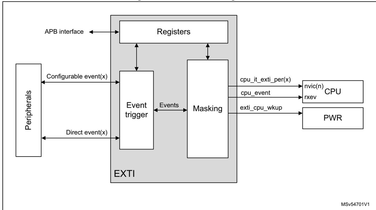
20.2.1 EXTI connections between peripherals and CPU
The peripherals able to generate wake-up events when the system is in Stop mode or the CPU is in CStop mode are connected to an EXTI configurable event input or direct event input:
- • Peripheral signals that generate a pulse are connected to an EXTI configurable event input. For these events the EXTI provides a CPU status pending bit that has to be cleared.
- • Peripheral interrupt and wake-up sources that have to be cleared in the peripheral are connected to an EXTI direct event input. There is no CPU status pending bit within the EXTI. The interrupt or wake-up is cleared by the CPU in the peripheral.
The CPU interrupts are connected to their respective CPU NVIC, and, similarly, the CPU event is connected to the CPU rxev input.
The EXTI wake-up signals are connected to the PWR block, and are used to wake up the CPU.
20.3 EXTI functional description
Depending on the EXTI event input type and wake-up target(s), different logic implementations are used. The applicable features are controlled from register bits:
- • Active trigger edge enable, by EXTI rising trigger selection register (EXTI_RTSR1) , EXTI rising trigger selection register (EXTI_RTSR2) , EXTI interrupt mask register (EXTI_IMR1) , and EXTI falling trigger selection register (EXTI_FTSR1) , EXTI falling trigger selection register (EXTI_FTSR2) , EXTI interrupt mask register (EXTI_IMR1)
- • Software trigger, by EXTI software interrupt event register (EXTI_SWIER1) , EXTI software interrupt event register (EXTI_SWIER2) , EXTI interrupt mask register (EXTI_IMR1)
- • CPU interrupt enable, by EXTI interrupt mask register (EXTI_IMR1) , EXTI interrupt mask register (EXTI_IMR2) , EXTI interrupt mask register (EXTI_IMR3)
- • CPU event enable, by EXTI event mask register (EXTI_EMR1) , EXTI interrupt mask register (EXTI_IMR2) , EXTI event mask register (EXTI_EMR3)
Table 143. EXTI event input configurations and register control (1)
| Event input type | Wake-up target(s) | Logic implementation | EXTI_RTSR | EXTI_FTSR | EXTI_SWIER | EXTI_IMR | EXTI_EMR |
|---|---|---|---|---|---|---|---|
| Configurable | CPU | Configurable event input, CPU wake-up logic | X | X | X | X | X |
| Direct | CPU | Direct event input, CPU wake-up logic | - | - | - | X | X |
1. X indicates that functionality is available.
20.3.1 EXTI configurable event input - CPU wake-up
Figure 20.3.2 is a detailed representation of the logic associated with configurable event inputs which always wake up the CPU.
Figure 156. Configurable event triggering logic CPU wake-up
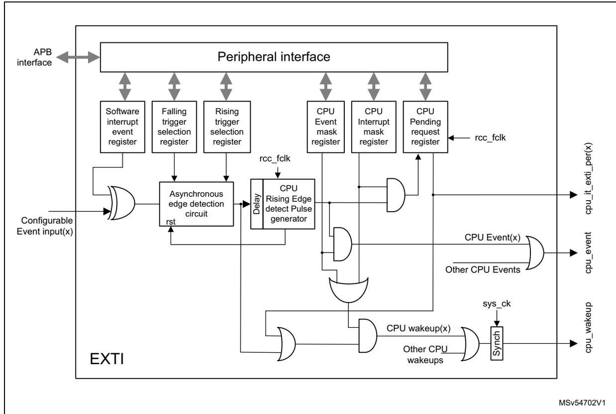
The software interrupt event register allows the system to trigger configurable events by software, writing the EXTI software interrupt event register (EXTI_SWIER1) , the EXTI software interrupt event register (EXTI_SWIER2) , or the EXTI interrupt mask register (EXTI_IMR1) register bit.
The rising edge EXTI rising trigger selection register (EXTI_RTSR1) , EXTI rising trigger selection register (EXTI_RTSR2) , EXTI interrupt mask register (EXTI_IMR1) , and falling edge EXTI falling trigger selection register (EXTI_FTSR1) , EXTI falling trigger selection register (EXTI_FTSR2) , EXTI interrupt mask register (EXTI_IMR1) selection registers allow the system to enable and select the configurable event active trigger edge or both edges.
The devices feature dedicated interrupt mask registers, namely EXTI interrupt mask register (EXTI_IMR1) and EXTI interrupt mask register (EXTI_IMR2) , EXTI interrupt mask register (EXTI_IMR3) , and EXTI pending register (EXTI_PR1) , EXTI pending register (EXTI_PR2) , for configurable event pending request registers. The CPU pending register is only set for an unmasked CPU interrupt. Each event provides a individual CPU interrupt to the CPU NVIC. The configurable event interrupts need to be acknowledged by software in the EXTI_PR register.
The devices feature dedicated event mask registers, i.e. EXTI event mask register (EXTI_EM1) , EXTI interrupt mask register (EXTI_IMR2) , and EXTI event mask register (EXTI_EM3) . The enabled event then generates an event on the CPU. All events for a CPU are OR-ed together into a single CPU event signal. The CPU pending register (EXTI_PR) is not set for an unmasked CPU event.
When a CPU interrupt or CPU event is enabled, the asynchronous edge detection circuit is reset by the clocked delay and rising edge detect pulse generator. This guarantees that the CPU clock is woken up before the asynchronous edge detection circuit is reset.
Note: A detected configurable event, enabled by the CPU, is only cleared when the CPU wakes up.
20.3.2 EXTI direct event input - CPU wake up
Figure 157 is a detailed representation of the logic associated with direct event inputs waking up the CPU.
Direct events only provide CPU interrupt enable and CPU event enable functionality.
Figure 157. Direct event triggering logic CPU wake up
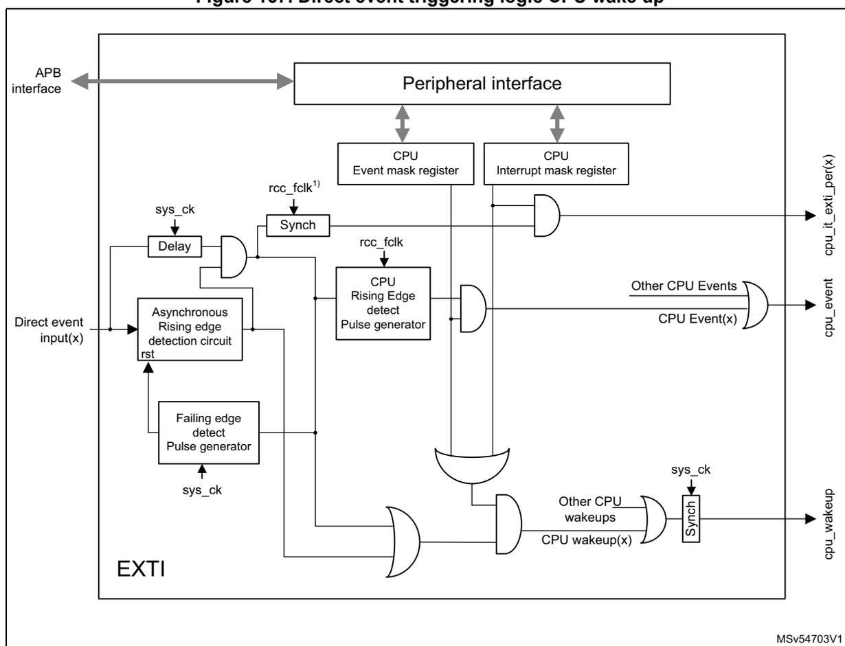
- 1. The CPU interrupt for asynchronous direct event inputs (peripheral wake-up signals) is synchronized with the CPU clock. The synchronous direct event inputs (peripheral interrupt signals), after the asynchronous edge detection, are directly sent to the CPU interrupt without resynchronization.
20.4 EXTI event input mapping
For the sixteen GPIO event inputs the associated IOPORT pin has to be selected in the SBS register SBS_EXTICRn. The same pin from each IOPORT maps to the corresponding EXTI event input.
The wake-up capabilities of each event input are detailed in Table 144 . An event input can wake up the CPU.
The EXTI event inputs with a connection to the CPU NVIC are indicated in the Connection to NVIC column. For the EXTI events not having a connection to the NVIC, the peripheral interrupt is directly connected to the NVIC in parallel with the connection to the EXTI.
All EXTI event inputs are OR-ed together and connected to the CPU event input (rxev).
Table 144. EXTI event input mapping
| Event input | Source | Event input type | Connection to NVIC |
|---|---|---|---|
| 0 - 15 | EXTI[15:0] | Configurable | Yes |
| 16 | PVD and AVD (1) | Configurable | Yes |
| 17 | RTC alarms, | Configurable | Yes |
| 18 | RTC tamper, RTC timestamp, LSE_CSS (2) | Configurable | Yes |
| 19 | RTC wake-up timer | Configurable | Yes |
| 20 | VBUS_FS_PLUG_UNPLUG | Configurable | Yes (3) |
| 21 | VBUS_HS_PLUG_UNPLUG | Configurable | Yes (3) |
| 22 | I2C1 wake-up | Direct | Yes |
| 23 | I2C2 wake-up | Direct | Yes |
| 24 | I2C3 wake-up | Direct | Yes |
| 25 | I3C1 wake-up | Direct | Yes |
| 26 | USART1 wake-up | Direct | Yes |
| 27 | USART2 wake-up | Direct | Yes |
| 28 | USART3 wake-up | Direct | Yes |
| 29 | Reserved | - | - |
| 30 | UART4 wake-up | Direct | Yes |
| 31 | UART5 wake-up | Direct | Yes |
| 32 | UART7 wake-up | Direct | Yes |
| 33 | UART8 wake-up | Direct | Yes |
| 34 | ADF wake-up | Configurable | Yes |
| 35 | LPUART1 wake-up | Direct | Yes |
| 36 | SPI1 wake-up | Direct | Yes |
| 37 | SPI2 wake-up | Direct | Yes |
| 38 | SPI3 wake-up | Direct | Yes |
| 39 | SPI4 wake-up | Direct | Yes |
Table 144. EXTI event input mapping (continued)
| Event input | Source | Event input type | Connection to NVIC |
|---|---|---|---|
| 40 | SPI5 wake-up | Direct | Yes |
| 41 | SPI6 wake-up | Direct | Yes |
| 42 | MDIO wake-up | Direct | Yes |
| 43 | USB_OTG_FS wake-up | Direct | Yes |
| 44 | USB_OTG_HS wake-up | Direct | Yes |
| 45 | UCPD wake-up | Direct | Yes |
| 46 | ETH_wake-up (3) | Configurable | Yes |
| 47 | LPTIM1 wake-up | Direct | Yes |
| 48 | LPTIM2 wake-up | Direct | Yes |
| 49 | LPTIM2 CH1 | Configurable | Yes |
| 50 | LPTIM3 wake-up | Direct | Yes |
| 51 | LPTIM3 CH1 | Configurable | Yes |
| 52 | LPTIM4 wake-up | Direct | Yes |
| 53 | LPTIM5 wake-up | Direct | Yes |
| 54 | HDMI-CEC wake-up | Configurable | Yes |
| 55 | WKUP1 | Direct | Yes |
| 56 | WKUP2 | Direct | Yes |
| 57 | WKUP3 | Direct | Yes |
| 58 | WKUP4 | Direct | Yes |
| 59 | WGLS wake-up | Direct | Yes |
| 60 | Reserved | - | - |
| 61 | Reserved | - | - |
| 62 | Reserved | - | - |
| 63 | Reserved | - | - |
| 64 | Reserved | - | - |
| 65 | Reserved | - | - |
| 66 | Reserved | - | - |
| 67 | Reserved | - | - |
| 68 | Reserved | - | - |
| 69 | Reserved | - | - |
| 70 | Reserved | - | - |
| 71 | Reserved | - | - |
| 72 | Reserved | - | - |
| 73 | Reserved | - | - |
| 74 | Reserved | - | - |
Table 144. EXTI event input mapping (continued)
| Event input | Source | Event input type | Connection to NVIC |
|---|---|---|---|
| 75 | Reserved | - | - |
| 76 | Reserved | - | - |
| 77 | DTS wake-up | Direct | Yes |
| 78 | Reserved | - | - |
| 79 | Reserved | - | - |
| 80 | Reserved | - | - |
- 1. PVD and AVD signals are OR-ed together on the same EXTI event input.
- 2. RTC Tamper, RTC timestamp and LSE_CSS are OR-ed together on the same EXTI event input.
- 3. lpi_intr_o OR pmt_intr_o
20.5 EXTI functional behavior
The direct event inputs are enabled in the respective peripheral generating the event. The configurable events are enabled by enabling at least one of the trigger edges.
An event only wakes up the CPU when the event-associated CPU interrupt is unmasked and/or the CPU event is unmasked.
Table 145. Masking functionality
| CPU | Configurable event inputs PRx bits of EXTI_PR | CPU | |||
|---|---|---|---|---|---|
| Interrupt enable MRx bits of EXTI_IMR | Event enable MRx bits of EXTI_EMR | Interrupt | Event | Wake-up | |
| 0 | 0 | No | Masked | Masked | Masked |
| 0 | 1 | No | Masked | Yes | Yes |
| 1 | 0 | Status latched | Yes | Masked | Yes |
| 1 | 1 | Status latched | Yes | Yes | Yes |
For configurable event inputs, when the enabled edge(s) occur on the event input, an event request is generated. When the associated CPU interrupt is unmasked, the corresponding pending PRx bit in EXTI_PR is set and the CPU interrupt signal is activated. EXTI_PR PRx pending bit must be cleared by software writing it to '1'. This clears the CPU interrupt.
For direct event inputs, when enabled in the associated peripheral, an event request is generated on the rising edge only. There is no corresponding CPU pending bit. When the associated CPU interrupt is unmasked the corresponding CPU interrupt signal is activated.
The CPU event has to be unmasked to generate an event. When the enabled edge(s) occur on the event input a CPU event pulse is generated. There is no CPU event pending bit.
Both a CPU interrupt and a CPU event may be enabled on the same event input. They both trigger the same event input condition(s).
For the configurable event inputs an event input request can be generated by software when writing a '1' in the software interrupt/event register EXTI_SWIER.
20.5.1 EXTI CPU interrupt procedure
- • Unmask the event input interrupt by setting the corresponding mask bits in the EXTI_IMR register.
- • For configurable event inputs, enable the event input by setting either one or both the corresponding trigger edge enable bits in EXTI_RTSR and EXTI_FTSR registers.
- • Enable the associated interrupt source in the CPU NVIC or use the SEVONPEND, so that an interrupt coming from the CPU interrupt signal is detectable by the CPU after a WFI/WFE instruction.
- – For configurable event inputs the associated EXTI pending bit needs to be cleared.
20.5.2 EXTI CPU event procedure
- • Unmask the event input by setting the corresponding mask bits of the EXTI_EMR register.
- • For configurable event inputs, enable the event input by setting either one or both the corresponding trigger edge enable bits in EXTI_RTSR and EXTI_FTSR registers.
- • The CPU event signal is detected by the CPU after a WFE instruction.
- – For configurable event inputs there is no EXTI pending bit to clear.
20.5.3 EXTI CPU wake-up procedure
- • Unmask the event input by setting at least one of the corresponding mask bits in the EXTI_IMR and/or EXTI_EMR registers. The CPU wake-up is generated at the same time as the unmasked CPU interrupt and/or CPU event.
- • For configurable event inputs, enable the event input by setting either one or both of the corresponding trigger edge enable bits in the EXTI_RTSR and EXTI_FTSR registers.
- • Direct events automatically generate a CPU wake-up.
20.5.4 EXTI software interrupt/event trigger procedure
Any of the configurable event inputs can be triggered from the software interrupt/event register (the associated CPU interrupt and/or CPU event must be enabled by their respective procedure).
- • Enable the event input by setting at least one of the corresponding edge trigger bits in the EXTI_RTSR and/or EXTI_FTSR registers.
- • Unmask the software interrupt/event trigger by setting at least one of the corresponding mask bits in the EXTI_IMR and/or EXTI_EMR registers.
- • Trigger the software interrupt/event by writing “1” to the corresponding bit in the EXTI_SWIER register.
- • The event input may be disabled by clearing the EXTI_RTSR and EXTI_FTSR register bits.
Note: An edge on the configurable event input also triggers an interrupt/event.
20.6 EXTI registers
The registers can only be accessed with a 32-bit (word). A byte or half-word cannot be read or written.
20.6.1 EXTI rising trigger selection register (EXTI_RTSR1)
Address offset: 0x00
Reset value: 0x0000 0000
| 31 | 30 | 29 | 28 | 27 | 26 | 25 | 24 | 23 | 22 | 21 | 20 | 19 | 18 | 17 | 16 |
|---|---|---|---|---|---|---|---|---|---|---|---|---|---|---|---|
| Res. | Res. | Res. | Res. | Res. | Res. | Res. | Res. | Res. | Res. | RT21 | RT20 | RT19 | RT18 | RT17 | RT16 |
| rw | rw | rw | rw | rw | rw | ||||||||||
| 15 | 14 | 13 | 12 | 11 | 10 | 9 | 8 | 7 | 6 | 5 | 4 | 3 | 2 | 1 | 0 |
| RT15 | RT14 | RT13 | RT12 | RT11 | RT10 | RT9 | RT8 | RT7 | RT6 | RT5 | RT4 | RT3 | RT2 | RT1 | RT0 |
| rw | rw | rw | rw | rw | rw | rw | rw | rw | rw | rw | rw | rw | rw | rw | rw |
Bits 31:22 Reserved, must be kept at reset value.
Bits 21:0 RT[21:0] : Rising trigger event configuration bit of configurable event input x. (1)
0: Rising trigger disabled (for event and interrupt) for input line
1: Rising trigger enabled (for event and interrupt) for input line
- The configurable event inputs are edge triggered, no glitch must be generated on these inputs.
If a rising edge on the configurable event input occurs during writing of the register, the associated pending bit is not set.
Rising and falling edge triggers can be set for the same configurable event input. In this case, both edges generate a trigger.
20.6.2 EXTI falling trigger selection register (EXTI_FTSR1)
Address offset: 0x04
Reset value: 0x0000 0000
| 31 | 30 | 29 | 28 | 27 | 26 | 25 | 24 | 23 | 22 | 21 | 20 | 19 | 18 | 17 | 16 |
|---|---|---|---|---|---|---|---|---|---|---|---|---|---|---|---|
| Res. | Res. | Res. | Res. | Res. | Res. | Res. | Res. | Res. | Res. | FT21 | FT20 | FT19 | FT18 | FT17 | FT16 |
| rw | rw | rw | rw | rw | rw | ||||||||||
| 15 | 14 | 13 | 12 | 11 | 10 | 9 | 8 | 7 | 6 | 5 | 4 | 3 | 2 | 1 | 0 |
| FT15 | FT14 | FT13 | FT12 | FT11 | FT10 | FT9 | FT8 | FT7 | FT6 | FT5 | FT4 | FT3 | FT2 | FT1 | FT0 |
| rw | rw | rw | rw | rw | rw | rw | rw | rw | rw | rw | rw | rw | rw | rw | rw |
Bits 31:22 Reserved, must be kept at reset value.
Bits 21:0 FT[21:0] : Falling trigger event configuration bit of configurable event input x. (1)
0: Falling trigger disabled (for event and interrupt) for input line
1: Falling trigger enabled (for event and interrupt) for input line.
- The configurable event inputs are edge triggered, no glitch must be generated on these inputs.
If a falling edge on the configurable event input occurs during writing of the register, the associated pending bit is not set.
Rising and falling edge triggers can be set for the same configurable event input. In this case, both edges generate a trigger.
20.6.3 EXTI software interrupt event register (EXTI_SWIER1)
Address offset: 0x08
Reset value: 0x0000 0000
| 31 | 30 | 29 | 28 | 27 | 26 | 25 | 24 | 23 | 22 | 21 | 20 | 19 | 18 | 17 | 16 |
|---|---|---|---|---|---|---|---|---|---|---|---|---|---|---|---|
| Res. | Res. | Res. | Res. | Res. | Res. | Res. | Res. | Res. | Res. | SW 21 | SW 20 | SW 19 | SW 18 | SW 17 | SW 16 |
| rw | rw | rw | rw | rw | rw |
| 15 | 14 | 13 | 12 | 11 | 10 | 9 | 8 | 7 | 6 | 5 | 4 | 3 | 2 | 1 | 0 |
|---|---|---|---|---|---|---|---|---|---|---|---|---|---|---|---|
| SW 15 | SW 14 | SW 13 | SW 12 | SW 11 | SW 10 | SW9 | SW8 | SW7 | SW6 | SW5 | SW4 | SW3 | SW2 | SW1 | SW0 |
| rw | rw | rw | rw | rw | rw | rw | rw | rw | rw | rw | rw | rw | rw | rw | rw |
Bits 31:22 Reserved, must be kept at reset value.
Bits 21:0 SWx : Software interrupt on event x (x = 21 to 0).
This bitfield always returns 0 when read.
0: Writing 0 has no effect.
1: Writing a 1 to this bit triggers an event on line x. This bit is auto cleared by HW.
20.6.4 EXTI rising trigger selection register (EXTI_RTSR2)
Address offset: 0x20
Reset value: 0x0000 0000
| 31 | 30 | 29 | 28 | 27 | 26 | 25 | 24 | 23 | 22 | 21 | 20 | 19 | 18 | 17 | 16 |
|---|---|---|---|---|---|---|---|---|---|---|---|---|---|---|---|
| Res. | Res. | Res. | Res. | Res. | Res. | Res. | Res. | Res. | RT54 | Res. | Res. | RT51 | Res. | RT49 | Res. |
| rw | rw | rw |
| 15 | 14 | 13 | 12 | 11 | 10 | 9 | 8 | 7 | 6 | 5 | 4 | 3 | 2 | 1 | 0 |
|---|---|---|---|---|---|---|---|---|---|---|---|---|---|---|---|
| Res. | RT46 | Res. | Res. | Res. | Res. | Res. | Res. | Res. | Res. | Res. | Res. | Res. | RT34 | Res. | Res. |
| rw | rw |
Bits 31:23 Reserved, must be kept at reset value.
Bit 22 RT54 : Rising trigger event configuration bit of configurable event input x+32. (1)
0: Rising trigger disabled (for event and interrupt) for input line
1: Rising trigger enabled (for event and interrupt) for input line
Bits 21:20 Reserved, must be kept at reset value.
Bit 19 RT51 : Rising trigger event configuration bit of configurable event input x+32. (1)
0: Rising trigger disabled (for event and interrupt) for input line
1: Rising trigger enabled (for event and interrupt) for input line
Bit 18 Reserved, must be kept at reset value.
Bit 17 RT49 : Rising trigger event configuration bit of configurable event input x+32. (1)
0: Rising trigger disabled (for event and interrupt) for input line
1: Rising trigger enabled (for event and interrupt) for input line
Bits 16:15 Reserved, must be kept at reset value.
Bit 14 RT46 : Rising trigger event configuration bit of configurable event input x+32. (1)
0: Rising trigger disabled (for event and interrupt) for input line
1: Rising trigger enabled (for event and interrupt) for input line
Bits 13:3 Reserved, must be kept at reset value.
Bit 2 RT34 : Rising trigger event configuration bit of configurable event input x+32. (1)
0: Rising trigger disabled (for event and interrupt) for input line
1: Rising trigger enabled (for event and interrupt) for input line
Bits 1:0 Reserved, must be kept at reset value.
- 1. The configurable event inputs are edge triggered, no glitch must be generated on these inputs.
If a rising edge on the configurable event input occurs during writing of the register, the associated pending bit is not set.
Rising and falling edge triggers can be set for the same configurable event input. In this case, both edges generate a trigger.
20.6.5 EXTI falling trigger selection register (EXTI_FTSR2)
Address offset: 0x24
Reset value: 0x0000 0000
| 31 | 30 | 29 | 28 | 27 | 26 | 25 | 24 | 23 | 22 | 21 | 20 | 19 | 18 | 17 | 16 |
|---|---|---|---|---|---|---|---|---|---|---|---|---|---|---|---|
| Res. | Res. | Res. | Res. | Res. | Res. | Res. | Res. | Res. | FT54 | Res. | Res. | FT51 | Res. | FT49 | Res. |
| 15 | 14 | 13 | 12 | 11 | 10 | 9 | 8 | 7 | 6 | 5 | 4 | 3 | 2 | 1 | 0 |
| Res. | FT46 | Res. | Res. | Res. | Res. | Res. | Res. | Res. | Res. | Res. | Res. | Res. | FT34 | Res. | Res. |
| rw | rw |
Bits 31:23 Reserved, must be kept at reset value.
Bit 22 FT54 : Falling trigger event configuration bit of configurable event input x+32. (1)
0: Falling trigger disabled (for event and interrupt) for input line
1: Falling trigger enabled (for event and interrupt) for input line
Bits 21:20 Reserved, must be kept at reset value.
Bit 19 FT51 : Falling trigger event configuration bit of configurable event input x+32. (1)
0: Falling trigger disabled (for event and interrupt) for input line
1: Falling trigger enabled (for event and interrupt) for input line
Bit 18 Reserved, must be kept at reset value.
Bit 17 FT49 : Falling trigger event configuration bit of configurable event input x+32. (1)
0: Falling trigger disabled (for event and interrupt) for input line
1: Falling trigger enabled (for event and interrupt) for input line
Bits 16:15 Reserved, must be kept at reset value.
Bit 14 FT46 : Falling trigger event configuration bit of configurable event input x+32. (1)
0: Falling trigger disabled (for event and interrupt) for input line
1: Falling trigger enabled (for event and interrupt) for input line
Bits 13:3 Reserved, must be kept at reset value.
Bit 2 FT34 : Falling trigger event configuration bit of configurable event input x+32. (1)
0: Falling trigger disabled (for event and interrupt) for input line
1: Falling trigger enabled (for event and interrupt) for input line
Bits 1:0 Reserved, must be kept at reset value.
- 1. The configurable event inputs are edge triggered, no glitch must be generated on these inputs.
If a falling edge on the configurable event input occurs during writing of the register, the associated pending bit is not set.
Rising and falling edge triggers can be set for the same configurable event input. In this case, both edges generate a trigger.
20.6.6 EXTI software interrupt event register (EXTI_SWIER2)
Address offset: 0x28
Reset value: 0x0000 0000
| 31 | 30 | 29 | 28 | 27 | 26 | 25 | 24 | 23 | 22 | 21 | 20 | 19 | 18 | 17 | 16 |
|---|---|---|---|---|---|---|---|---|---|---|---|---|---|---|---|
| Res. | Res. | Res. | Res. | Res. | Res. | Res. | Res. | Res. | SW 54 | Res. | Res. | SW 51 | Res. | SW 49 | Res. |
| rw | rw | rw |
| 15 | 14 | 13 | 12 | 11 | 10 | 9 | 8 | 7 | 6 | 5 | 4 | 3 | 2 | 1 | 0 |
|---|---|---|---|---|---|---|---|---|---|---|---|---|---|---|---|
| Res. | SW 46 | Res. | Res. | Res. | Res. | Res. | Res. | Res. | Res. | Res. | Res. | Res. | SW 34 | Res. | Res. |
| rw | rw |
Bits 31:23 Reserved, must be kept at reset value.
Bit 22 SW54 : Software interrupt on event x+32
Always returns 0 when read.
0: Writing 0 has no effect.
1: Writing a 1 to this bit triggers an event on line x. This bit is auto cleared by HW.
Bits 21:20 Reserved, must be kept at reset value.
Bit 19 SW51 : Software interrupt on event x+32
Always returns 0 when read.
0: Writing 0 has no effect.
1: Writing a 1 to this bit triggers an event on line x. This bit is auto cleared by HW.
Bit 18 Reserved, must be kept at reset value.
Bit 17 SW49 : Software interrupt on event x+32
Always returns 0 when read.
0: Writing 0 has no effect.
1: Writing a 1 to this bit triggers an event on line x. This bit is auto cleared by HW.
Bits 16:15 Reserved, must be kept at reset value.
Bit 14 SW46 : Software interrupt on event x+32
Always returns 0 when read.
0: Writing 0 has no effect.
1: Writing a 1 to this bit triggers an event on line x. This bit is auto cleared by HW.
Bits 13:3 Reserved, must be kept at reset value.
Bit 2 SW34 : Software interrupt on event x+32
Always returns 0 when read.
0: Writing 0 has no effect.
1: Writing a 1 to this bit triggers an event on line x. This bit is auto cleared by HW.
Bits 1:0 Reserved, must be kept at reset value.
20.6.7 EXTI interrupt mask register (EXTI_IMR1)
Address offset: 0x80
Reset value: 0xFFC0 0000
| 31 | 30 | 29 | 28 | 27 | 26 | 25 | 24 | 23 | 22 | 21 | 20 | 19 | 18 | 17 | 16 |
|---|---|---|---|---|---|---|---|---|---|---|---|---|---|---|---|
| IM31 | IM30 | IM29 | IM28 | IM27 | IM26 | IM25 | IM24 | IM23 | IM22 | IM21 | IM20 | IM19 | IM18 | IM17 | IM16 |
| rw | rw | rw | rw | rw | rw | rw | rw | rw | rw | rw | rw | rw | rw | rw | rw |
| 15 | 14 | 13 | 12 | 11 | 10 | 9 | 8 | 7 | 6 | 5 | 4 | 3 | 2 | 1 | 0 |
| IM15 | IM14 | IM13 | IM12 | IM11 | IM10 | IM9 | IM8 | IM7 | IM6 | IM5 | IM4 | IM3 | IM2 | IM1 | IM0 |
| rw | rw | rw | rw | rw | rw | rw | rw | rw | rw | rw | rw | rw | rw | rw | rw |
Bits 31:22 IM[31:22] : CPU interrupt mask on direct event input x (1)
0: Interrupt request from line x is masked
1: Interrupt request from line x is unmasked
Bits 21:0 IM[21:0] : CPU interrupt mask on configurable event input x (2)
0: Interrupt request from line x is masked
1: Interrupt request from line x is unmasked
- 1. The reset value for direct event inputs is set to '1' in order to enable the interrupt by default.
- 2. The reset value for configurable event inputs is set to '0' in order to disable the interrupt by default.
20.6.8 EXTI event mask register (EXTI_EMR1)
Address offset: 0x84
Reset value: 0x0000 0000
| 31 | 30 | 29 | 28 | 27 | 26 | 25 | 24 | 23 | 22 | 21 | 20 | 19 | 18 | 17 | 16 |
|---|---|---|---|---|---|---|---|---|---|---|---|---|---|---|---|
| EM31 | EM30 | EM29 | EM28 | EM27 | EM26 | EM25 | EM24 | EM23 | EM22 | EM21 | EM20 | EM19 | EM18 | EM17 | EM16 |
| rw | rw | rw | rw | rw | rw | rw | rw | rw | rw | rw | rw | rw | rw | rw | rw |
| 15 | 14 | 13 | 12 | 11 | 10 | 9 | 8 | 7 | 6 | 5 | 4 | 3 | 2 | 1 | 0 |
| EM15 | EM14 | EM13 | EM12 | EM11 | EM10 | EM9 | EM8 | EM7 | EM6 | EM5 | EM4 | EM3 | EM2 | EM1 | EM0 |
| rw | rw | rw | rw | rw | rw | rw | rw | rw | rw | rw | rw | rw | rw | rw | rw |
Bits 31:0
EM[31:0]
: CPU
event
mask on event input x
0: Event request from line x is masked
1: Event request from line x is unmasked
20.6.9 EXTI pending register (EXTI_PR1)
Address offset: 0x88
Reset value: 0xXXXX XXXX
| 31 | 30 | 29 | 28 | 27 | 26 | 25 | 24 | 23 | 22 | 21 | 20 | 19 | 18 | 17 | 16 |
|---|---|---|---|---|---|---|---|---|---|---|---|---|---|---|---|
| Res. | Res. | Res. | Res. | Res. | Res. | Res. | Res. | Res. | Res. | PR21 | PR20 | PR19 | PR18 | PR17 | PR16 |
| rc_w1 | rc_w1 | rc_w1 | rc_w1 | rc_w1 | rc_w1 | ||||||||||
| 15 | 14 | 13 | 12 | 11 | 10 | 9 | 8 | 7 | 6 | 5 | 4 | 3 | 2 | 1 | 0 |
| PR15 | PR14 | PR13 | PR12 | PR11 | PR10 | PR9 | PR8 | PR7 | PR6 | PR5 | PR4 | PR3 | PR2 | PR1 | PR0 |
| rc_w1 | rc_w1 | rc_w1 | rc_w1 | rc_w1 | rc_w1 | rc_w1 | rc_w1 | rc_w1 | rc_w1 | rc_w1 | rc_w1 | rc_w1 | rc_w1 | rc_w1 | rc_w1 |
Bits 31:22 Reserved, must be kept at reset value.
Bits 21:0
PR[21:0]
: Configurable event inputs x Pending bit
0: No trigger request occurred
1: selected trigger request occurred
This bit is set when the selected edge event arrives on the external interrupt line. This bit is cleared by writing a 1 into the bit or by changing the sensitivity of the edge detector.
20.6.10 EXTI interrupt mask register (EXTI_IMR2)
Address offset: 0x90
Reset value: 0xFFFF5 FFFF
| 31 | 30 | 29 | 28 | 27 | 26 | 25 | 24 | 23 | 22 | 21 | 20 | 19 | 18 | 17 | 16 |
|---|---|---|---|---|---|---|---|---|---|---|---|---|---|---|---|
| Res. | Res. | Res. | Res. | IM59 | IM58 | IM57 | IM56 | IM55 | IM54 | IM53 | IM52 | IM51 | IM50 | IM49 | IM48 |
| 15 | 14 | 13 | 12 | 11 | 10 | 9 | 8 | 7 | 6 | 5 | 4 | 3 | 2 | 1 | 0 |
| IM47 | IM46 | IM45 | IM44 | IM43 | IM42 | IM41 | IM40 | IM39 | IM38 | IM37 | IM36 | IM35 | IM34 | IM33 | IM32 |
| rw | rw | rw | rw | rw | rw | rw | rw | rw | rw | rw | rw | rw | rw | rw | rw |
Bits 31:28 Reserved, must be kept at reset value.
Bits 27:0 IM[59:32] : CPU interrupt mask on direct event input x+32 (x = 59 to 32)
0: Interrupt request from line x is masked
1: Interrupt request from line x is unmasked
20.6.11 EXTI event mask register (EXTI_EMR2)
Address offset: 0x94
Reset value: 0x0000 0000
| 31 | 30 | 29 | 28 | 27 | 26 | 25 | 24 | 23 | 22 | 21 | 20 | 19 | 18 | 17 | 16 |
|---|---|---|---|---|---|---|---|---|---|---|---|---|---|---|---|
| Res. | Res. | Res. | Res. | EM59 | EM58 | EM57 | EM56 | EM55 | EM54 | EM53 | EM52 | EM51 | EM50 | EM49 | EM48 |
| 15 | 14 | 13 | 12 | 11 | 10 | 9 | 8 | 7 | 6 | 5 | 4 | 3 | 2 | 1 | 0 |
| EM47 | EM46 | EM45 | EM44 | EM43 | EM42 | EM41 | EM40 | EM39 | EM38 | EM37 | EM36 | EM35 | EM34 | EM33 | EM32 |
| rw | rw | rw | rw | rw | rw | rw | rw | rw | rw | rw | rw | rw | rw | rw | rw |
Bits 31:28 Reserved, must be kept at reset value.
Bits 27:0 EM[59:32] : CPU event mask on event input x+32 (x = 59 to 32)
0: Event request from line x is masked
1: Event request from line x is unmasked
20.6.12 EXTI pending register (EXTI_PR2)
Address offset: 0x98
Reset value: 0xXXXX XXXX
| 31 | 30 | 29 | 28 | 27 | 26 | 25 | 24 | 23 | 22 | 21 | 20 | 19 | 18 | 17 | 16 |
|---|---|---|---|---|---|---|---|---|---|---|---|---|---|---|---|
| Res. | Res. | Res. | Res. | Res. | Res. | Res. | Res. | Res. | PR54 | Res. | Res. | PR51 | Res. | PR49 | Res. |
| rc_w1 | rc_w1 | rc_w1 | |||||||||||||
| 15 | 14 | 13 | 12 | 11 | 10 | 9 | 8 | 7 | 6 | 5 | 4 | 3 | 2 | 1 | 0 |
| Res. | PR46 | Res. | Res. | Res. | Res. | Res. | Res. | Res. | Res. | Res. | Res. | Res. | PR34 | Res. | Res. |
| rc_w1 | rc_w1 |
Bits 31:23 Reserved, must be kept at reset value.
Bit 22 PR54 : Configurable event inputs x+32 Pending bit
0: No trigger request occurred
1: selected trigger request occurred
This bit is set when the selected edge event arrives on the external interrupt line. This bit is cleared by writing a 1 into the bit or by changing the sensitivity of the edge detector.
Bits 21:20 Reserved, must be kept at reset value.
Bit 19 PR51 : Configurable event inputs x+32 Pending bit
0: No trigger request occurred
1: selected trigger request occurred
This bit is set when the selected edge event arrives on the external interrupt line. This bit is cleared by writing a 1 into the bit or by changing the sensitivity of the edge detector.
Bit 18 Reserved, must be kept at reset value.
Bit 17 PR49 : Configurable event inputs x+32 Pending bit
0: No trigger request occurred
1: selected trigger request occurred
This bit is set when the selected edge event arrives on the external interrupt line. This bit is cleared by writing a 1 into the bit or by changing the sensitivity of the edge detector.
Bits 16:15 Reserved, must be kept at reset value.
Bit 14 PR46 : Configurable event inputs x+32 Pending bit
0: No trigger request occurred
1: selected trigger request occurred
This bit is set when the selected edge event arrives on the external interrupt line. This bit is cleared by writing a 1 into the bit or by changing the sensitivity of the edge detector.
Bits 13:3 Reserved, must be kept at reset value.
Bit 2 PR34 : Configurable event inputs x+32 Pending bit
0: No trigger request occurred
1: selected trigger request occurred
This bit is set when the selected edge event arrives on the external interrupt line. This bit is cleared by writing a 1 into the bit or by changing the sensitivity of the edge detector.
Bits 1:0 Reserved, must be kept at reset value.
20.6.13 EXTI interrupt mask register (EXTI_IMR3)
Address offset: 0xA0
Reset value: 0x0F8B FFFF
| 31 | 30 | 29 | 28 | 27 | 26 | 25 | 24 | 23 | 22 | 21 | 20 | 19 | 18 | 17 | 16 |
|---|---|---|---|---|---|---|---|---|---|---|---|---|---|---|---|
| Res. | Res. | Res. | Res. | Res. | Res. | Res. | Res. | Res. | Res. | Res. | Res. | Res. | Res. | Res. | Res. |
| 15 | 14 | 13 | 12 | 11 | 10 | 9 | 8 | 7 | 6 | 5 | 4 | 3 | 2 | 1 | 0 |
| Res. | Res. | IM77 | Res. | Res. | Res. | Res. | Res. | Res. | Res. | Res. | Res. | Res. | Res. | Res. | Res. |
| rw |
Bits 31:14 Reserved, must be kept at reset value.
Bit 13 IM[77] : CPU interrupt mask on direct event input x+64 (1)
0: Interrupt request from line x is masked
1: Interrupt request from line x is unmasked
Bits 12:0 Reserved, must be kept at reset value.
- 1. The reset value for direct event inputs is set to '1' in order to enable the interrupt by default.
20.6.14 EXTI event mask register (EXTI_EMR3)
Address offset: 0xA4
Reset value: 0x0000 0000
| 31 | 30 | 29 | 28 | 27 | 26 | 25 | 24 | 23 | 22 | 21 | 20 | 19 | 18 | 17 | 16 |
|---|---|---|---|---|---|---|---|---|---|---|---|---|---|---|---|
| Res. | Res. | Res. | Res. | Res. | Res. | Res. | Res. | Res. | Res. | Res. | Res. | Res. | Res. | Res. | Res. |
| 15 | 14 | 13 | 12 | 11 | 10 | 9 | 8 | 7 | 6 | 5 | 4 | 3 | 2 | 1 | 0 |
| Res. | Res. | EM77 | Res. | Res. | Res. | Res. | Res. | Res. | Res. | Res. | Res. | Res. | Res. | Res. | Res. |
| rw |
Bits 31:14 Reserved, must be kept at reset value.
Bit 13 EM[77] : CPU event mask on event input x+64
0: Event request from line x is masked
1: Event request from line x is unmasked
Bits 12:0 Reserved, must be kept at reset value.
20.6.15 EXTI register map
Table 146. Extended interrupt and event controller register map and reset values
| Offset | Register name reset value | 31 | 30 | 29 | 28 | 27 | 26 | 25 | 24 | 23 | 22 | 21 | 20 | 19 | 18 | 17 | 16 | 15 | 14 | 13 | 12 | 11 | 10 | 9 | 8 | 7 | 6 | 5 | 4 | 3 | 2 | 1 | 0 |
|---|---|---|---|---|---|---|---|---|---|---|---|---|---|---|---|---|---|---|---|---|---|---|---|---|---|---|---|---|---|---|---|---|---|
| 0x00 | EXTI_RTSR1 | Res. | Res. | Res. | Res. | Res. | Res. | Res. | Res. | Res. | Res. | RT21 | RT20 | RT19 | RT18 | RT17 | RT16 | RT15 | RT14 | RT13 | RT12 | RT11 | RT10 | RT9 | RT8 | RT7 | RT6 | RT5 | RT4 | RT3 | RT2 | RT1 | RT0 |
| Reset value | 0 | 0 | 0 | 0 | 0 | 0 | 0 | 0 | 0 | 0 | 0 | 0 | 0 | 0 | 0 | 0 | 0 | 0 | 0 | 0 | 0 | 0 | |||||||||||
| 0x04 | EXTI_FTSR1 | Res. | Res. | Res. | Res. | Res. | Res. | Res. | Res. | Res. | Res. | FT21 | FT20 | FT19 | FT18 | FT17 | FT16 | FT15 | FT14 | FT13 | FT12 | FT11 | FT10 | FT9 | FT8 | FT7 | FT6 | FT5 | FT4 | FT3 | FT2 | FT1 | FT0 |
| Reset value | 0 | 0 | 0 | 0 | 0 | 0 | 0 | 0 | 0 | 0 | 0 | 0 | 0 | 0 | 0 | 0 | 0 | 0 | 0 | 0 | 0 | 0 | |||||||||||
| 0x08 | EXTI_SWIER1 | Res. | Res. | Res. | Res. | Res. | Res. | Res. | Res. | Res. | Res. | SW21 | SW20 | SW19 | SW18 | SW17 | SW16 | SW15 | SW14 | SW13 | SW12 | SW11 | SW10 | SW9 | SW8 | SW7 | SW6 | SW5 | SW4 | SW3 | SW2 | SW1 | SW0 |
| Reset value | 0 | 0 | 0 | 0 | 0 | 0 | 0 | 0 | 0 | 0 | 0 | 0 | 0 | 0 | 0 | 0 | 0 | 0 | 0 | 0 | 0 | 0 | |||||||||||
| 0x12-0x1C | Reserved | ||||||||||||||||||||||||||||||||
| 0x20 | EXTI_RTSR2 | Res. | Res. | Res. | Res. | Res. | Res. | Res. | Res. | Res. | RT54 | Res. | Res. | RT51 | Res. | RT49 | Res. | Res. | RT46 | Res. | Res. | Res. | Res. | Res. | Res. | Res. | Res. | Res. | Res. | Res. | RT34 | Res. | Res. |
| Reset value | 0 | 0 | 0 | 0 | 0 | ||||||||||||||||||||||||||||
| 0x24 | EXTI_FTSR2 | Res. | Res. | Res. | Res. | Res. | Res. | Res. | Res. | Res. | FT54 | Res. | Res. | FT51 | Res. | FT49 | Res. | Res. | FT46 | Res. | Res. | Res. | Res. | Res. | Res. | Res. | Res. | Res. | Res. | Res. | FT34 | Res. | Res. |
| Reset value | 0 | 0 | 0 | 0 | 0 | ||||||||||||||||||||||||||||
| 0x28 | EXTI_SWIER2 | Res. | Res. | Res. | Res. | Res. | Res. | Res. | Res. | Res. | SW54 | Res. | Res. | SW51 | Res. | SW49 | Res. | Res. | SW46 | Res. | Res. | Res. | Res. | Res. | Res. | Res. | Res. | Res. | Res. | Res. | SW34 | Res. | Res. |
| Reset value | 0 | 0 | 0 | 0 | 0 | ||||||||||||||||||||||||||||
| 0x2C-0x7C | Reserved | ||||||||||||||||||||||||||||||||
| 0x80 | EXTI_IMR1 | IM31 | IM30 | IM29 | IM28 | IM27 | IM26 | IM25 | IM24 | IM23 | IM22 | IM21 | IM20 | IM19 | IM18 | IM17 | IM16 | IM15 | IM14 | IM13 | IM12 | IM11 | IM10 | IM9 | IM8 | IM7 | IM6 | IM5 | IM4 | IM3 | IM2 | IM1 | IM0 |
| Reset value | 1 | 1 | 1 | 1 | 1 | 1 | 1 | 1 | 1 | 1 | 0 | 0 | 0 | 0 | 0 | 0 | 0 | 0 | 0 | 0 | 0 | 0 | 0 | 0 | 0 | 0 | 0 | 0 | 0 | 0 | 0 | 0 | |
| 0x84 | EXTI_EMR1 | EM31 | EM30 | EM29 | EM28 | EM27 | EM26 | EM25 | EM24 | EM23 | EM22 | EM21 | EM20 | EM19 | EM18 | EM17 | EM16 | EM15 | EM14 | EM13 | EM12 | EM11 | EM10 | EM9 | EM8 | EM7 | EM6 | EM5 | EM4 | EM3 | EM2 | EM1 | EM0 |
| Reset value | 0 | 0 | 0 | 0 | 0 | 0 | 0 | 0 | 0 | 0 | 0 | 0 | 0 | 0 | 0 | 0 | 0 | 0 | 0 | 0 | 0 | 0 | 0 | 0 | 0 | 0 | 0 | 0 | 0 | 0 | 0 | 0 | |
| 0x88 | EXTI_PR1 | Res. | Res. | Res. | Res. | Res. | Res. | Res. | Res. | Res. | Res. | PR21 | PR20 | PR19 | PR18 | PR17 | PR16 | PR15 | PR14 | PR13 | PR12 | PR11 | PR10 | PR9 | PR8 | PR7 | PR6 | PR5 | PR4 | PR3 | PR2 | PR1 | PR0 |
| Reset value | X | X | X | X | X | X | X | X | X | X | X | X | X | X | X | X | X | X | X | X | X | X | |||||||||||
| 0x90 | EXTI_IMR2 | Res. | Res. | Res. | Res. | IM59 | IM58 | IM57 | IM56 | IM55 | IM54 | IM53 | IM52 | IM51 | IM50 | IM49 | IM48 | IM47 | IM46 | IM45 | IM44 | IM43 | IM42 | IM41 | IM40 | IM39 | IM38 | IM37 | IM36 | IM35 | IM34 | IM33 | IM32 |
| Reset value | 1 | 1 | 1 | 1 | 1 | 1 | 1 | 1 | 0 | 1 | 0 | 1 | 1 | 1 | 1 | 1 | 1 | 1 | 1 | 1 | 1 | 1 | 1 | 1 | 1 | 1 | 1 | 1 | |||||
| 0x94 | EXTI_EMR2 | Res. | Res. | Res. | Res. | EM59 | EM58 | EM57 | EM56 | EM55 | EM54 | EM53 | EM52 | EM51 | EM50 | EM49 | EM48 | EM47 | EM46 | EM45 | EM44 | EM43 | EM42 | EM41 | EM40 | EM39 | EM38 | EM37 | EM36 | EM35 | EM34 | EM33 | EM32 |
| Reset value | 0 | 0 | 0 | 0 | 0 | 0 | 0 | 0 | 0 | 0 | 0 | 0 | 0 | 0 | 0 | 0 | 0 | 0 | 0 | 0 | 0 | 0 | 0 | 0 | 0 | 0 | 0 | 0 | |||||
| 0x98 | EXTI_PR2 | Res. | Res. | Res. | Res. | Res. | Res. | Res. | Res. | Res. | PR54 | Res. | Res. | PR51 | Res. | PR49 | Res. | Res. | PR46 | Res. | Res. | Res. | Res. | Res. | Res. | Res. | Res. | Res. | Res. | Res. | PR34 | Res. | Res. |
| Reset value | X | X | X | X | X | ||||||||||||||||||||||||||||
| 0x9C | Reserved | ||||||||||||||||||||||||||||||||
Table 146. Extended interrupt and event controller register map and reset values (continued)
| Offset | Register name reset value | 31 | 30 | 29 | 28 | 27 | 26 | 25 | 24 | 23 | 22 | 21 | 20 | 19 | 18 | 17 | 16 | 15 | 14 | 13 | 12 | 11 | 10 | 9 | 8 | 7 | 6 | 5 | 4 | 3 | 2 | 1 | 0 |
|---|---|---|---|---|---|---|---|---|---|---|---|---|---|---|---|---|---|---|---|---|---|---|---|---|---|---|---|---|---|---|---|---|---|
| 0xA0 | EXTI_IMR3 | Res. | Res. | Res. | Res. | Res. | Res. | Res. | Res. | Res. | Res. | Res. | Res. | Res. | Res. | Res. | Res. | Res. | Res. | IM77 | Res. | Res. | Res. | Res. | Res. | Res. | Res. | Res. | Res. | Res. | Res. | Res. | Res. |
| Reset value | 1 | ||||||||||||||||||||||||||||||||
| 0xA4 | EXTI_EMR3 | Res. | Res. | Res. | Res. | Res. | Res. | Res. | Res. | Res. | Res. | Res. | Res. | Res. | Res. | Res. | Res. | Res. | Res. | EM77 | Res. | Res. | Res. | Res. | Res. | Res. | Res. | Res. | Res. | Res. | Res. | Res. | Res. |
| Reset value | 0 |
Refer to Section 2.3 on page 150 for the register boundary addresses.