18. Graphic timer (GFXTIM)
18.1 GFXTIM introduction
The graphic timer (GFXTIM) is a graphic oriented timer allowing smart management of graphical events for frame or line counting.
18.2 GFXTIM main features
- • Integrated frame and line-clock generation
- • One absolute frame counter with one compare channel
- • Two auto-reload relative frame counters
- • One line timer with two compare channels
- • External tearing-effect line management and synchronization
- • Four programmable event generators with external trigger generation
- • One watchdog counter
18.3 GFXTIM functional description
18.3.1 Block diagram
The graphic timer is split into six functional blocks
- • Clock generator
- • Absolute timers
- • Relative timers
- • Tearing-effect detection
- • Event generators
- • Watchdog timer
Figure 140. GFXTIM block diagram
![Figure 140. GFXTIM block diagram. This block diagram illustrates the internal architecture of the GFXTIM. It shows various functional blocks: 'Control and status' (Int. registers), 'Clock generator' (with TE Detect, Auto-reload, 22-bit line-clock counter, 12-bit frame-clock counter), 'Absolute timer' (20-bit frame counter, 12-bit line counter, Compare 1 register, Compare 2 register), 'Event Generators' (4 generators), 'Relative timers' (Auto-reload 1, Auto-reload 2, 12-bit frame counter 1, 12-bit frame counter 2), and 'Watchdog timer' (Auto-reload, 16-bit counter, Pre-alarm). Pins on the left include GFXTIM_TE, gfxtim_ite, gfxtim_hsync[3:0], gfxtim_vsync[3:0], gfxtim_it, gfxtim_wdg_it, gfxtim_hclk, gfxtim_ev1, gfxtim_ev2, gfxtim_ev3, gfxtim_ev4, gfxtim_wrld, GFXTIM_FCKCAL, and GFXTIM_LCKCAL. A 32-bit APB bus connects to the control and status and absolute timer blocks. A legend at the bottom indicates 'Frame-clock domain' in blue and 'Line-clock domain' in green.](/RM0477-STM32H7Rx-7Sx/ad4959c4da20622fd6cda2502407b5a7_img.jpg)
MSV66908V3
18.3.2 GFXTIM pins and internal signals
Table 137. GFXTIM input/output pins
| Pin name | Signal type | Description |
|---|---|---|
| GFXTIM_TE | Input | Tearing effect |
| GFXTIM_FCKCAL | Output | Frame-clock calibration output |
| GFXTIM_LCKCAL | Output | line-clock calibration output |
Table 138. GFXTIM internal signals
| Signal name | Signal type | Description |
|---|---|---|
| gfxtim_hclk | Digital input | Kernel and register interface clock |
| gfxtim_it | Digital output | Global interrupt |
| gfxtim_wdg_it | Digital output | Watchdog interrupt |
| gfxtim_ev1 | Digital output | Graphic timer event 1 |
| gfxtim_ev2 | Digital output | Graphic timer event 2 |
| gfxtim_ev3 | Digital output | Graphic timer event 3 |
| gfxtim_ev4 | Digital output | Graphic timer event 4 |
| gfxtim_wrld | Digital input | Watchdog reload |
| gfxtim_ite | Digital input | Internal tearing effect |
| Signal name | Signal type | Description |
|---|---|---|
| gfxtim_hsync[3:0] | Digital input | Horizontal synchronization |
| gfxtim_vsync[3:0] | Digital input | Vertical synchronization |
The table below shows how GFXTIM triggers are connected.
Table 139. GFXTIM trigger interconnections| Trigger name | Direction | Trigger source/destination |
|---|---|---|
| gfxtim_ev1 | Output | hpdma_trigsel[20] |
| gfxtim_ev2 | Output | hpdma_trigsel[19] |
| gfxtim_ev3 | Output | hpdma_trigsel[18] |
| gfxtim_ev4 | Output | hpdma_trigsel[17] |
| gfxtim_wrld | Input | reserved |
| gfxtim_ite | Input | reserved |
| gfxtim_hsync[0] | Input | LCD_HSYNC |
| gfxtim_hsync[1] | Input | dcmipp_p0_hsync_evt |
| gfxtim_hsync[2] | Input | reserved |
| gfxtim_hsync[3] | Input | reserved |
| gfxtim_vsync[0] | Input | LCD_VSYNC |
| gfxtim_vsync[1] | Input | dcmipp_p0_vsync_evt |
| gfxtim_vsync[2] | Input | reserved |
| gfxtim_vsync[3] | Input | reserved |
18.3.3 Clock generator
Two clocks are generated internally to fed the absolute and relative timers:
- • the frame-clock: clocking frame counters
- • the line-clock: clocking line counters
Internal counter for time base generation
The GFXTIM embeds a two-clock generation counter:
- • a 22-bit auto-reload down-counter on the system clock
- • a 12-bit auto-reload down-counter on selectable internal or external event
Figure 141. Clock generator
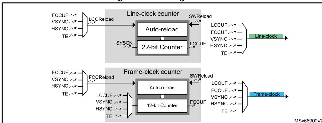
Line-clock counter
The line-clock counter is a 22-bit auto-reload down-counter on the system clock.
The line-clock counter is enabled selecting its clock source with LCCCS (line-clock counter clock source) in GFXTIM_CGCR (clock generator control register).
The line-clock counter can be reloaded automatically when one of the following event occurs:
- • frame-clock counter underflows
- • VSYNC edge (with control of polarity)
- • HSYNC edge (with control of polarity)
- • TE edge (with control of polarity)
The hardware reload function and source can be selected with LCCHRS (line-clock counter hardware reload source) in GFXTIM_CGCR (clock generator control register).
The line-clock counter can be reloaded by software, setting LCCFR (line-clock counter force reload) in GFXTIM_CGCR (clock generator control register).
The reload value is programmed in GFXTIM_LCCRR (line-clock counter reload register).
Frame-clock counter
The frame-clock counter is an 12-bit auto-reload down-counter clocked by either, TE, HSYNC, VSYNC or a line-clock counter underflow.
The frame-clock counter is enabled selecting its clock source with FCCCS in GFXTIM_CGCR.
The frame-clock counter can be reloaded automatically when one of the following event occurs:
- • line-clock counter underflow
- • VSYNC edge (with control of polarity)
- • HSYNC edge (with control of polarity)
- • TE edge (with control of polarity)
The hardware reload function and source can be selected with FCCHRS in GFXTIM_CGCR.
The frame-clock counter can be reloaded by software, setting FCCFR in GFXTIM_CGCR.
The reload value is programmed in GFXTIM_FCCRR.
Clock generation
The line-clock source can be one of the following:
- • underflow flag of the internal 22-bit down-counter
- • underflow flag of the internal 12-bit down-counter
- • HSYNC, VSYNC or TE pin (with control of polarity)
The frame-clock source can be one of the following:
- • underflow flag of the internal 22-bit down-counter
- • underflow flag of the internal 12-bit down-counter
- • HSYNC, VSYNC or TE pin (with control of polarity)
Clock calibration output
For calibration/debug purpose, the frame-clock and line-clock can be output on a specific I/O.
The frame-clock calibration output is enabled by setting FCCOE (frame-clock calibration output enable) in GFXTIM_CR (configuration register).
The line-clock calibration output is enabled by setting LCCOE in GFXTIM_CR.
Synchronization and tearing-effect sources
The GFXTIM can be connected to peripherals providing HSYNC and/or VSYNC synchronization signals, like the LCD-TFT controller or the camera interface.
The source of HSYNC and/or VSYNC is selected through SYNCS (synchronization source) in GFXTIM_CR.
The tearing-effect source can be an external pin or can be provided by the MIPI® DSI Host on system embedding this interface. To extend the orthogonality versus the synchronization signals, the tearing-effect source can be also the selected HSYNC or VSYNC input.
The tearing-effect source can be selected with TES (TE source) in GFXTIM_CR.
18.3.4 Example of clock generator configuration
The clock generator can have several configuration to work:
- • in standalone (without any external synchronization)
- • with external HSYNC and VSYNC
- • with external HSYNC only
- • with external VSYNC only
- • with external CSYNC (TE) only
The synchronization signals, HSYNC, VSYNC and TE, are symmetrical in the implementation and can be exchanged if needed.
The set of examples detailed below are given for reference, but other combinations can be programmed into the clock generator.
Standalone
In standalone configuration, the clock generator provides to the GFXTIM, the frame-clock and the line-clock without any external signals.
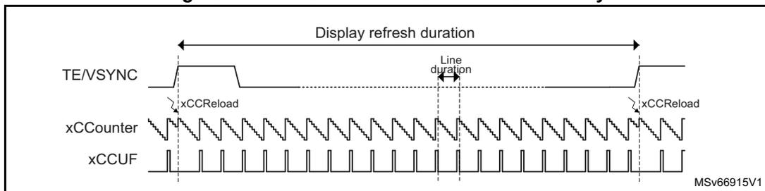
Figure 142. Waveforms in standalone
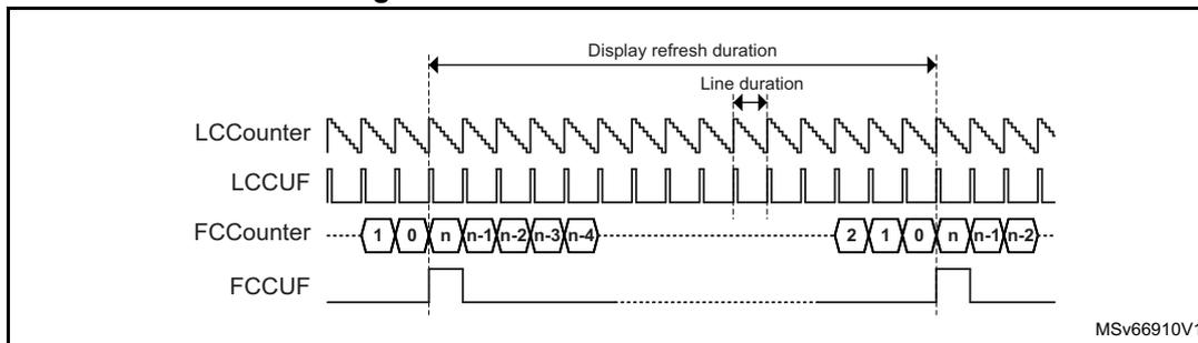
The LCCUF (line-clock counter underflow) event acts as line-clock and the FCCUF (frame-clock counter underflow) acts as frame-clock.
The clock generator can be synchronized by one of the following ways:
- • by software reload, setting the FCCFR in GFXTIM_CGCR.
- • by hardware reload on an external VSYNC (or TE)
Figure 143. Active counters and signals in standalone

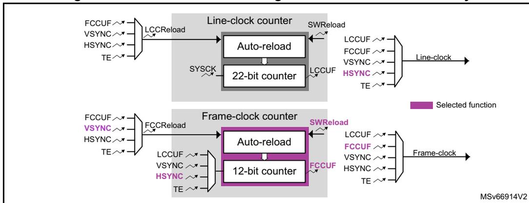
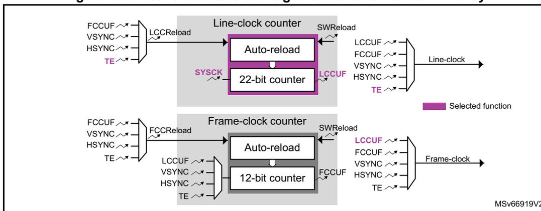
External HSYNC and VSYNC
When using external HSYNC and VSYNC, the counters are not used for the line and frame-clock generation. The clock generator copy directly HSYNC to the line-clock and VSYNC to the frame-clock.
Figure 144. Waveforms with external HSYNC and VSYNC
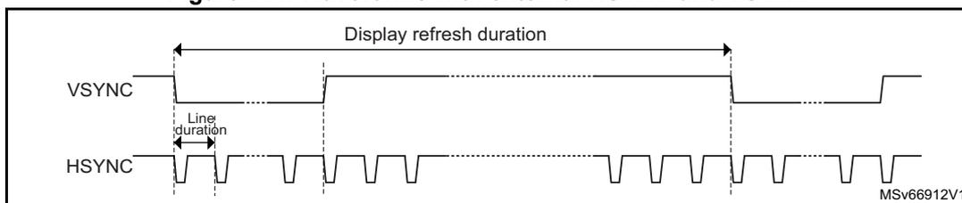
HSYNC acts as line-clock and VSYNC acts as frame-clock.
External HSYNC only
With external HSYNC only, the clock generator provides to the GFXTIM, the frame-clock and the line-clock based only on HSYNC.
Figure 145. Waveforms with external HSYNC only
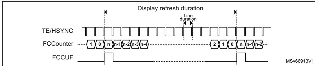
HSYNC acts as line-clock and FCCUF acts as frame-clock.
The clock generator can be synchronized by one of the following ways:
- • by software reload, setting FCCFR in GFXTIM_CGCR
- • by hardware reload on an external VSYNC (or TE)
Figure 146. Active counters and signals with external HSYNC only
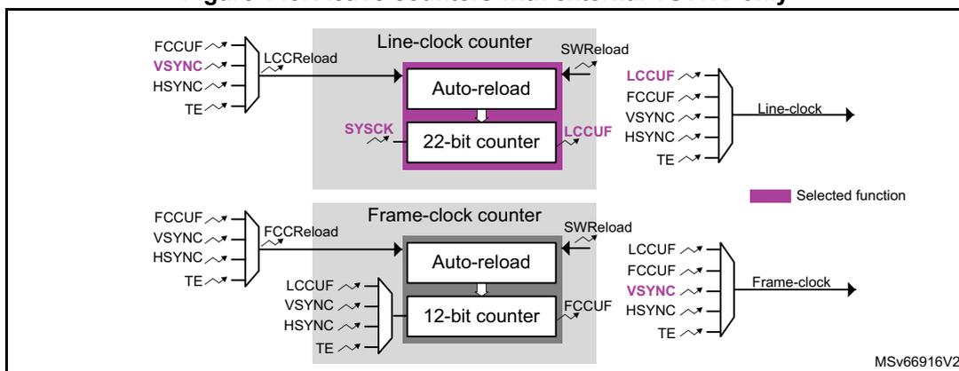
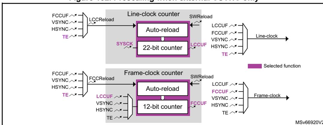
External VSYNC only
With external VSYNC only, the clock generator provides to the GFXTIM, the frame-clock and the line-clock based only on VSYNC.
Figure 147. Waveforms with external VSYNC only
LCCUF (line-clock counter underflow) acts as line-clock and VSYNC acts as frame-clock.
The line-clock counter generating the line-clock is reloaded on VSYNC event.
Figure 148. Active counters with external VSYNC only
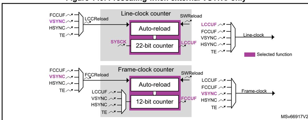
The line-clock counter can also act as a prescaler for the frame-clock counter to have a wider range of counting. FCCUF acts as line-clock.
Figure 149. Prescaling when external VSYNC only
External CSYNC only
With external CSYNC only, the clock generator provides to the GFXTIM, the frame-clock and the line-clock based only on CSYNC (in the following figures, CSYNC is input on TE).
Figure 150. Waveforms with external CSYNC only
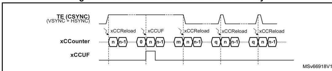
The CSYNC (on TE pin in this example) acts as line-clock and LCCUF acts as frame-clock. The line-clock counter generating the frame-clock is reloaded on CSYNC event.
Figure 151. Active counters and signals with external CSYNC only
The line-clock counter can also act as a prescaler for the frame-clock counter to have a wider range of counting. FCCUF acts as frame-clock.
Figure 152. Prescaling when external CSYNC only
18.3.5 Absolute timers
Absolute time
The absolute time 32-bit value can be read directly in GFXTIM_ATR (absolute time register) to provide a global time and to generate absolute time accurate event to synchronize the graphical software.
The absolute time is generated by the combination of:
- • the absolute frame counter
- • the absolute line counter
Absolute frame counter
The absolute frame counter is a 20-bit free running up-counter with a software controlled reset.
It can be enabled by writing 1 in AFCEN (absolute-frame counter enable) of GFXTIM_TCR (timers configuration register).
The counter is incremented at each rising edge of the frame-clock and is reset by setting FAFCR (force absolute-frame counter reset) in GFXTIM_TCR.
In case of overflow of the absolute frame counter, AFCOF (overflow flag) is set in GFXTIM_ISR (interrupt status register), and an interrupt is generated if AFCOIE (overflow interrupt enable) is set in (interrupt enable register).
A 20-bit compare register can generate an absolute-frame counter compare event when the counter value matches the compare value. When a compare event occurs, AFCC1F (compare 1 flag) is set in GFXTIM_ISR, and an interrupt is generated if AFCC1IE (compare 1 interrupt enable) is set in GFXTIM_IER.
The absolute frame counter can be disabled by writing 1 in AFCDIS (counter disable) of GFXTIM_TDR (timers disable register).
The status (enabled/disabled) can be monitored through AFCS (counter status) in GFXTIM_TSR (timers status register).
Absolute line counter
The absolute line counter is 12-bit free running-up counter with an hardware controlled reset.
It can be enabled by writing 1 in ALCEN of GFXTIM_TCR.
The counter is incremented at each rising edge of the line-clock and is reset at each rising edge of the frame-clock or setting FALCR in GFXTIM_TCR).
In case of overflow of the absolute line counter, ALCOF is set in GFXTIM_ISR, and an interrupt is generated if ALCOIE is set in GFXTIM_IER.
Two 12-bit compare registers can generate an absolute line counter compare events when the counter value matches the compare value. When a compare event occurs, ALCC1F or ALCC2F is set in GFXTIM_ISR, and an interrupt is generated if ALCC1IE or ALCC2IE is set in GFXTIM_IER.
The absolute line counter can be disabled writing 1 in ALCDIS of GFXTIM_TDR.
The status (enabled/disabled) can be monitored through ALCS in GFXTIM_TSR.
18.3.6 Relative timers
The relative timers can generate periodic events to synchronize the graphical tasks at frame level.
The relative frame counters are 12-bit down-counting auto-reload timers that are decremented at each rising edge of the frame-clock. The counter is started by writing 1 in RFCxEN (relative frame counter x enable) of GFXTIM_TCR. The starting value is automatically loaded from GFXTIM_RFCxRR (relative frame counter x reload register).
The current relative frame counter value can be read directly in GFXTIM_RFCxR.
Once the counter reaches zero, it is automatically reloaded with the value of GFXTIM_RFCxRR. RFCxRF (reload flag) is set in GFXTIM_ISR, and an interrupt is generated if RFCxRIE (interrupt enable) is set in GFXTIM_IER.
Once the reload operation occurs, the timer can be disabled automatically or continue counting if RFCxCM (continuous mode) is set in GFXTIM_TCR.
The status (enabled/disabled) can be monitored through RFCxS in GFXTIM_TSR.
The counter can be reloaded on the fly by setting FRFCRx in GFXTIM_TCR. This force reload neither stop the timer (even if RFCxCN = 0 in GFXTIM_TCR), nor set RFCxRF (reload flag) in GFXTIM_ISR.
The relative frame counter can be disabled by setting RFCxDIS (disable) in GFXTIM_TDR.
18.3.7 Tearing-effect detection
A tearing-effect line can work in one of the two configurations shown in the figure below.
Figure 153. Tearing-effect configurations
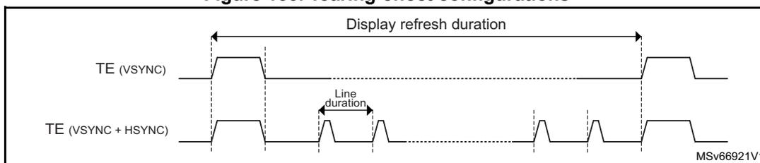
A tearing-effect event can be generated on rising or falling edge depending on TEPOL (tearing-effect polarity) in GFXTIM_CR.
When a tearing-effect event is detected, TEF (tearing-event flag) is set in GFXTIM_ISR, and an interrupt is generated if TEIE (interrupt enable) is set in GFXTIM_IER.
18.3.8 Event generator
The event generator can combine timer events into complex events. Up to four combined events can be generated.
The events can be used for:
- • interrupt generation
- • watchdog clocking
- • external trigger generation
A complex event is a combination between a frame event and a line event.
Once a frame event occurs, the GFXTIM waits for the line event to occur before generating the complex event.
The frame event is selected by the corresponding FESx (frame event selection x) in GFXTIM_EVSR (events selection y register). The line event is selected by the corresponding LESx in GFXTIM_EVSR.
The complex event generation is enabled by setting the corresponding EVxEN (event x enable) in GFXTIM_EVCR (event control register).
It is recommended to disable the event generation prior to any event configuration to avoid spurious complex event generation
When a complex event occurs, the corresponding EVxF (event x flag) is set in GFXTIM_ISR, and an interrupt is generated if EVxIE (event x interrupt enable) is set in GFXTIM_IER.
Each of the events can be connected to another peripherals (such as DMA) to generate hardware triggers.
18.3.9 Watchdog timer
The watchdog timer is a 16-bit auto-reload down-counter with a programmable clock source.
Figure 154. Watchdog timer

The diagram shows a 'Watchdog' block containing three stacked components: 'Auto-reload', '16-bit counter', and 'Pre-alarm'. On the left, multiple input lines are shown: 'Reload' (with a software symbol), 'Line-clock', 'Frame-clock', 'HSYNC', 'VSYNC', 'TE', 'EV1', 'EV2', 'EV3', and 'EV4'. These inputs are connected to the 'Auto-reload' and '16-bit counter' components. On the right, two output lines are shown: 'ALRM' and 'PALRM', which are connected to the '16-bit counter' and 'Pre-alarm' components respectively. The diagram is labeled 'MSV66922V2' in the bottom right corner.
Clock source
The watchdog clock source can be selected through WDGCS (clock source) in GTXTIM_WDGTCR (watchdog timer configuration register), between one of the following:
- • line-clock
- • frame-clock
- • HSYNC
- • VSYNC
- • TE
- • event 1
- • event 2
- • event 3
- • event 4
Startup
The watchdog is started by setting WDGEN in GFXTIM_WDGTCR and stops automatically when reaching 0.
On start, the watchdog counter is automatically loaded with the auto-reload value programmed in GFXTIM_WDGRR (watchdog reload register).
The current watchdog value can be read through GFXTIM_WDGCR.
Auto-reload
The auto-reload can be forced in one of the following ways:
- • by software, setting FWDGR (force watchdog reload) in GTXTIM_WDGTCR (watchdog timer configuration register)
- • by hardware through an external trigger (gfxtim_wrl0 signal)
The polarity of the trigger is configured by WDGHRC (watchdog hardware reload configuration) in GFXTIM_WDGTCR.
Event and interrupt generation
The watchdog can generate two events:
- • an alarm when the watchdog down-counter reaches 0
The watchdog counter is automatically stopped, and WDGAF (alarm flag) is set in GFXTIM_ISR. An interrupt is generated if WDGAIIE (alarm interrupt enable) is set in GFXTIM_IER. - • a pre-alarm when the watchdog counter matches the pre-alarm register value in GFXTIM_WDGPAR (watchdog pre-alarm register)
WDGPF (pre-alarm flag) is set in GFXTIM_ISR, and an interrupt is generated if WDGPIE (pre-alarm interrupt enable) is set in GFXTIM_IER.
18.4 GFXTIM interrupts
An interrupt can be produced on the following events:
- • absolute frame counter compare event
- • absolute frame counter overflow
- • absolute line counter compare events
- • absolute line counter overflow
- • relative frame counter reload events
- • external tearing effect
- • combined events
- • watchdog alarm event
- • watchdog pre-alarm event
Separate interrupt enable bits are available for flexibility.
Table 140. Graphic timer interrupt requests
| Interrupt acronym | Interrupt event | Event flag | Enable control bit | Interrupt clear method |
|---|---|---|---|---|
| GFXTIM | Absolute frame counter overflow | AFCOF | AFCOIE | write 1 in CAFCOF |
| Absolute frame counter compare 1 | AFCC1F | AFCC1IE | write 1 in CAFCC1F | |
| Absolute line counter overflow | ALCOF | ALCOIE | write 1 in CALCOF | |
| Absolute line counter compare 1 | ALCC1F | ALCC1IE | write 1 in CALCC1F | |
| Absolute line counter compare 2 | ALCC2F | ALCC2IE | write 1 in CALCC2F | |
| Relative frame counter 1 reload | RFC1RF | RFC1RIE | write 1 in CRFC1RF | |
| Relative frame counter 2 reload | RFC2RF | RFC2RIE | write 1 in CRFC2RF | |
| External tearing effect | TEF | TEIE | write 1 in CTEF | |
| Event 1 | EV1F | EV1IE | write 1 in CEV1F | |
| Event 2 | EV2F | EV2IE | write 1 in CEV2F | |
| Event 3 | EV3F | EV3IE | write 1 in CEV3F | |
| Event 4 | EV4F | EV4IE | write 1 in CEV4F |
Table 140. Graphic timer interrupt requests (continued)
| Interrupt acronym | Interrupt event | Event flag | Enable control bit | Interrupt clear method |
|---|---|---|---|---|
| GFXTIM_WDG | Watchdog alarm | WDGAF | WDGAIE | write 1 in CWDGAF |
| Watchdog pre-alarm | WDGPF | WDGPIE | write 1 in CWDGPF |
18.5 GFXTIM registers
18.5.1 GFXTIM configuration register (GFXTIM_CR)
Address offset: 0x000
Reset value: 0x0000 0000
| 31 | 30 | 29 | 28 | 27 | 26 | 25 | 24 | 23 | 22 | 21 | 20 | 19 | 18 | 17 | 16 |
|---|---|---|---|---|---|---|---|---|---|---|---|---|---|---|---|
| Res. | Res. | Res. | Res. | Res. | Res. | Res. | Res. | Res. | Res. | Res. | Res. | Res. | Res. | LCCOE | FCCOE |
| rw | rw | ||||||||||||||
| 15 | 14 | 13 | 12 | 11 | 10 | 9 | 8 | 7 | 6 | 5 | 4 | 3 | 2 | 1 | 0 |
| Res. | Res. | Res. | Res. | Res. | Res. | SYNCS[1:0] | Res. | Res. | Res. | TEPOL | Res. | Res. | Res. | TES[1:0] | |
| rw | rw | rw | rw | rw |
Bits 31:18 Reserved, must be kept at reset value.
Bit 17 LCCOE : Line-clock calibration output enable
This bit enables the line-clock output.
0: Line-clock output disabled
1: Line-clock output enabled
Bit 16 FCCOE : Frame-clock calibration output enable
This bit enables the frame-clock output.
0: Frame-clock output disabled
1: Frame-clock output enabled
Bits 15:10 Reserved, must be kept at reset value.
Bits 9:8 SYNCS[1:0] : Synchronization source
This bitfield selects the synchronization signals (HSYNC and VSYNC) sources.
00: gfxtim_hsync[0] and gfxtim_vsync[0] selected
01: gfxtim_hsync[1] and gfxtim_vsync[1] selected
10: gfxtim_hsync[2] and gfxtim_vsync[2] selected
11: gfxtim_hsync[3] and gfxtim_vsync[3] selected
Bits 7:5 Reserved, must be kept at reset value.
Bit 4 TEPOL : Tearing--effect polarity
This bit selects the tearing-effect polarity.
0: Tearing effect active on rising edge
1: Tearing effect active on falling edge
Bits 3:2 Reserved, must be kept at reset value.
Bits 1:0 TES[1:0] : Tearing source
This bitfield selects the tearing-effect source.
00: TE input pad selected
01: gfxtim_ite selected
10: HSYNC input selected by SYNCS[1:0]
11: VSYNC input selected by SYNCS[1:0]
18.5.2 GFXTIM clock generator configuration register (GFXTIM_CGCR)
Address offset: 0x004
Reset value: 0x0000 0000
| 31 | 30 | 29 | 28 | 27 | 26 | 25 | 24 | 23 | 22 | 21 | 20 | 19 | 18 | 17 | 16 |
|---|---|---|---|---|---|---|---|---|---|---|---|---|---|---|---|
| Res. | FCCHRS[2:0] | Res. | Res. | Res. | FCCFR | Res. | FCCCS[2:0] | Res. | FCS[2:0] | ||||||
| rw | rw | rw | w | rw | rw | rw | rw | rw | rw | ||||||
| 15 | 14 | 13 | 12 | 11 | 10 | 9 | 8 | 7 | 6 | 5 | 4 | 3 | 2 | 1 | 0 |
|---|---|---|---|---|---|---|---|---|---|---|---|---|---|---|---|
| Res. | LCCHRS[2:0] | Res. | Res. | Res. | LCCFR | Res. | Res. | Res. | LCCCS | Res. | LCS[2:0] | ||||
| rw | rw | rw | w | rw | rw | rw | rw | ||||||||
Bit 31 Reserved, must be kept at reset value.
Bits 30:28 FCCHRS[2:0] : Frame-clock counter hardware reload source
This bitfield configures the hardware reload source for the frame-clock counter.
000: No hardware reload
001: Line- clock counter underflow
010: HSYNC rising edge
011: HSYNC falling edge
100: VSYNC rising edge
101: VSYNC falling edge
110: TE rising edge
111: TE falling edge
Bits 27:25 Reserved, must be kept at reset value.
Bit 24 FCCFR : Frame-clock counter force reload
This bit forces frame-clock counter reload
0: No effect
1: Frame-clock counter reload forced
Bit 23 Reserved, must be kept at reset value.
Bits 22:20 FCCCS[2:0] : Frame-clock counter clock source
This bitfield configures the clock source for the frame-clock counter.
000: Frame-clock counter disabled
001: Line-clock counter underflow
010: HSYNC rising edge
011: HSYNC falling edge
100: VSYNC rising edge
101: VSYNC falling edge
110: TE rising edge
111: TE falling edge
Bit 19 Reserved, must be kept at reset value.
Bits 18:16 FCS[2:0] : Frame-clock source
This bitfield configures the frame-clock source.
- 000: Line-clock counter underflow
- 001: Frame-clock counter underflow
- 010: HSYNC rising edge
- 011: HSYNC falling edge
- 100: VSYNC rising edge
- 101: VSYNC falling edge
- 110: TE rising edge
- 111: TE falling edge
Bit 15 Reserved, must be kept at reset value.
Bits 14:12 LCCHRS[2:0] : Line-clock counter hardware reload source
This bitfield configures the hardware reload source for the line-clock counter.
- 000: No hardware reload
- 001: Frame-clock counter underflow
- 010: HSYNC rising edge
- 011: HSYNC falling edge
- 100: VSYNC rising edge
- 101: VSYNC falling edge
- 110: TE rising edge
- 111: TE falling edge
Bits 11:9 Reserved, must be kept at reset value.
Bit 8 LCCFR : Line-clock counter force reload
This bit forces line-clock counter reload.
- 0: No effect
- 1: Line-clock counter reload forced
Bits 7:5 Reserved, must be kept at reset value.
Bit 4 LCCCS : Line-clock counter clock source
This bit configures the clock source for the line-clock counter.
- 0: Line-clock counter disabled
- 1: System clock selected
Bit 3 Reserved, must be kept at reset value.
Bits 2:0 LCS[2:0] : Line-clock source
This bitfield configures the line-clock source.
- 000: Line-clock counter underflow
- 001: Frame-clock counter underflow
- 010: HSYNC rising edge
- 011: HSYNC falling edge
- 100: VSYNC rising edge
- 101: VSYNC falling edge
- 110: TE rising edge
- 111: TE falling edge
18.5.3 GFXTIM timers configuration register (GFXTIM_TCR)
Address offset: 0x008
Reset value: 0x0000 0000
| 31 | 30 | 29 | 28 | 27 | 26 | 25 | 24 | 23 | 22 | 21 | 20 | 19 | 18 | 17 | 16 |
|---|---|---|---|---|---|---|---|---|---|---|---|---|---|---|---|
| Res. | Res. | Res. | Res. | Res. | Res. | Res. | Res. | Res. | FRFC2R | RFC2CM | RFC2EN | Res. | FRFC1R | RFC1CM | RFC1EN |
| w | rw | w | w | rw | w | ||||||||||
| 15 | 14 | 13 | 12 | 11 | 10 | 9 | 8 | 7 | 6 | 5 | 4 | 3 | 2 | 1 | 0 |
| Res. | Res. | Res. | Res. | Res. | Res. | Res. | Res. | Res. | Res. | FALCR | ALCEN | Res. | Res. | FAFCR | AFCEN |
| w | w | w | w |
Bits 31:23 Reserved, must be kept at reset value.
Bit 22 FRFC2R : Force relative frame counter 2 reload
This bit forces the reload of the relative frame counter 2.
0: No effect
1: Relative frame counter 2 reload forced
Bit 21 RFC2CM : Relative frame counter 2 continuous mode
This bit enables the continuous mode of the relative frame counter 2.
0: Relative frame counter 2 is one shot.
1: Relative frame counter 2 is in continuous mode.
Bit 20 RFC2EN : Relative frame counter 2 enable
This bit enables the relative frame counter 2.
0: No effect
1: Relative frame counter 2 enabled
Bit 19 Reserved, must be kept at reset value.
Bit 18 FRFC1R : Force relative frame counter 1 reload
This bit forces the reload of the relative frame counter 1.
0: No effect
1: Relative frame counter 1 reload forced
Bit 17 RFC1CM : Relative frame counter 1 continuous mode
This bit enables the continuous mode of the relative frame counter 1.
0: Relative frame counter 1 is one shot.
1: Relative frame counter 1 is in continuous mode.
Bit 16 RFC1EN : Relative frame counter 1 enable
This bit enables the relative frame counter 1.
0: No effect
1: Relative frame counter enabled
Bits 15:6 Reserved, must be kept at reset value.
Bit 5 FALCR : Force absolute line counter reset
This bit forces the reset of the absolute line counter.
0: No effect
1: Absolute line counter reset forced
Bit 4 ALCEN : Absolute line counter enable
This bit enables the absolute line counter.
0: No effect
1: Absolute line counter enabled
Bits 3:2 Reserved, must be kept at reset value.
Bit 1 FAFCR : Force absolute frame counter reset
This bit forces the reset of the absolute frame counter.
0: No effect
1: Absolute frame counter reset forced
Bit 0 AFCEN : Absolute frame counter enable
This bit enables the absolute frame counter.
0: No effect
1: Absolute frame counter enabled
18.5.4 GFXTIM timers disable register (GFXTIM_TDR)
Address offset: 0x00C
Reset value: 0x0000 0000
| 31 | 30 | 29 | 28 | 27 | 26 | 25 | 24 | 23 | 22 | 21 | 20 | 19 | 18 | 17 | 16 |
|---|---|---|---|---|---|---|---|---|---|---|---|---|---|---|---|
| Res. | Res. | Res. | Res. | Res. | Res. | Res. | Res. | Res. | Res. | Res. | RFC2DIS | Res. | Res. | Res. | RFC1DIS |
| w | w | ||||||||||||||
| 15 | 14 | 13 | 12 | 11 | 10 | 9 | 8 | 7 | 6 | 5 | 4 | 3 | 2 | 1 | 0 |
| Res. | Res. | Res. | Res. | Res. | Res. | Res. | Res. | Res. | Res. | Res. | ALCDIS | Res. | Res. | Res. | AFCDIS |
| w | w |
Bits 31:21 Reserved, must be kept at reset value.
Bit 20 RFC2DIS : Relative frame counter 2 disable
This bit disables the relative frame counter 2.
0: No effect
1: Relative frame counter 2 disabled
Bits 19:17 Reserved, must be kept at reset value.
Bit 16 RFC1DIS : Relative frame counter 1 disable
This bit disables the relative frame counter 1.
0: No effect
1: Relative frame counter 1 disabled
Bits 15:5 Reserved, must be kept at reset value.
Bit 4 ALCDIS : Absolute line counter disable
This bit disables the absolute line counter.
0: No effect
1: Absolute line counter disabled
Bits 3:1 Reserved, must be kept at reset value.
- Bit 0
AFCDIS
: Absolute frame counter disable
This bit disables the absolute frame counter.
0: No effect
1: Absolute frame counter disabled
18.5.5 GFXTIM events control register (GFXTIM_EVCR)
Address offset: 0x010
Reset value: 0x0000 0000
| 31 | 30 | 29 | 28 | 27 | 26 | 25 | 24 | 23 | 22 | 21 | 20 | 19 | 18 | 17 | 16 |
|---|---|---|---|---|---|---|---|---|---|---|---|---|---|---|---|
| Res. | Res. | Res. | Res. | Res. | Res. | Res. | Res. | Res. | Res. | Res. | Res. | Res. | Res. | Res. | Res. |
| 15 | 14 | 13 | 12 | 11 | 10 | 9 | 8 | 7 | 6 | 5 | 4 | 3 | 2 | 1 | 0 |
| Res. | Res. | Res. | Res. | Res. | Res. | Res. | Res. | Res. | Res. | Res. | Res. | EV4EN rw | EV3EN rw | EV2EN rw | EV1EN rw |
Bits 31:4 Reserved, must be kept at reset value.
- Bit 3
EV4EN
: Event 4 enable
This bit enables the complex event 4 generation.
0: Event 4 generation disabled
1: Event 4 generation enabled - Bit 2
EV3EN
: Event 3 enable
This bit enables the complex event 3 generation.
0: Event 3 generation disabled
1: Event 3 generation enabled - Bit 1
EV2EN
: Event 2 enable
This bit enables the complex event 2 generation.
0: Event 2 generation disabled
1: Event 2 generation enabled - Bit 0
EV1EN
: Event 1 enable
This bit enables the complex event 1 generation.
0: Event 1 generation disabled
1: Event 1 generation enabled
18.5.6 GFXTIM events selection register (GFXTIM_EVSR)
Address offset: 0x014
Reset value: 0x0000 0000
| 31 | 30 | 29 | 28 | 27 | 26 | 25 | 24 | 23 | 22 | 21 | 20 | 19 | 18 | 17 | 16 |
|---|---|---|---|---|---|---|---|---|---|---|---|---|---|---|---|
| Res. | FES4[2:0] | Res. | LES4[2:0] | Res. | FES3[2:0] | Res. | LES3[2:0] | ||||||||
| rw | rw | rw | rw | rw | rw | rw | rw | rw | rw | rw | rw | ||||
| 15 | 14 | 13 | 12 | 11 | 10 | 9 | 8 | 7 | 6 | 5 | 4 | 3 | 2 | 1 | 0 |
| Res. | FES2[2:0] | Res. | LES2[2:0] | Res. | FES1[2:0] | Res. | LES1[2:0] | ||||||||
| rw | rw | rw | rw | rw | rw | rw | rw | rw | rw | rw | rw | ||||
Bit 31 Reserved, must be kept at reset value.
Bits 30:28 FES4[2:0] : Frame-event selection 4
This bitfield defines the frame-event selection for complex event 4 generation.
000: No frame event
001: Absolute frame counter overflow
010: Absolute frame counter compare
100: Relative frame counter 1 reload
101: Relative frame counter 2 reload
Others: Reserved
Bit 27 Reserved, must be kept at reset value.
Bits 26:24 LES4[2:0] : Line-event selection 4
This bitfield defines the line-event selection for complex event 4 generation.
000: No line event
001: Absolute line counter overflow
010: Tearing effect
100: Absolute line counter 1 compare
101: Absolute line counter 2 compare
Others: Reserved
Bit 23 Reserved, must be kept at reset value.
Bits 22:20 FES3[2:0] : Frame-event selection 3
This bitfield defines the frame-event selection for complex event 3 generation.
000: No frame event
001: Absolute frame counter overflow
010: Absolute frame counter compare
100: Relative frame counter 1 reload
101: Relative frame counter 2 reload
Others: Reserved
Bit 19 Reserved, must be kept at reset value.
Bits 18:16 LES3[2:0] : Line-event selection 3
This bitfield defines the line-event selection for complex event 3 generation.
000: No line event
001: Absolute line counter overflow
010: Tearing effect
100: Absolute line counter 1 compare
101: Absolute line counter 2 compare
Others: Reserved
Bit 15 Reserved, must be kept at reset value.
Bits 14:12 FES2[2:0] : Frame-event selection 2
This bitfield defines the frame-event selection for complex event 2 generation.
000: No frame event
001: Absolute frame counter overflow
010: Absolute frame counter compare
100: Relative frame counter 1 reload
101: Relative frame counter 2 reload
Others: Reserved
Bit 11 Reserved, must be kept at reset value.
Bits 10:8 LES2[2:0] : Line-event selection 2
This bitfield defines the line-event selection for complex event 2 generation.
000: No line event
001: Absolute line counter overflow
010: Tearing effect
100: Absolute line counter 1 compare
101: Absolute line counter 2 compare
Others: Reserved
Bit 7 Reserved, must be kept at reset value.
Bits 6:4 FES1[2:0] : Frame-event selection 1
This bitfield defines the frame-event selection for complex event 1 generation.
000: No frame event
001: Absolute frame counter overflow
010: Absolute frame counter compare
100: Relative frame counter 1 reload
101: Relative frame counter 2 reload
Others: Reserved
Bit 3 Reserved, must be kept at reset value.
Bits 2:0 LES1[2:0] : Line-event selection 1
This bitfield defines the line-event selection for complex event 1 generation.
000: No line event
001: Absolute line counter overflow
010: Tearing effect
100: Absolute line counter 1 compare
101: Absolute line counter 2 compare
Others: Reserved
18.5.7 GFXTIM watchdog timer configuration register (GFXTIM_WDGTCR)
Address offset: 0x020
Reset value: 0x0000 0000
| 31 | 30 | 29 | 28 | 27 | 26 | 25 | 24 | 23 | 22 | 21 | 20 | 19 | 18 | 17 | 16 |
|---|---|---|---|---|---|---|---|---|---|---|---|---|---|---|---|
| Res. | Res. | Res. | Res. | Res. | Res. | Res. | Res. | Res. | Res. | Res. | Res. | Res. | Res. | Res. | FWDGR |
| w | |||||||||||||||
| 15 | 14 | 13 | 12 | 11 | 10 | 9 | 8 | 7 | 6 | 5 | 4 | 3 | 2 | 1 | 0 |
| Res. | Res. | Res. | Res. | WDGCS[3:0] | Res. | Res. | WDGHRC[1:0] | Res. | WDGS | WDGDI S | WDGE N | ||||
| rw | rw | rw | rw | rw | rw | r | w | w | |||||||
Bits 31:17 Reserved, must be kept at reset value.
Bit 16 FWDGR : Force watchdog reload
This bit forces the reload of the graphic watchdog.
0: No effect
1: Graphic watchdog reload forced
Bits 15:12 Reserved, must be kept at reset value.
Bits 11:8 WDGCS[3:0] : Watchdog clock source
This bitfield selects the watchdog clock source.
0000: Line-clock
0001: Frame-clock
0010: HSYNC rising edge
0011: HSYNC falling edge
0100: VSYNC rising edge
0101: VSYNC falling edge
0110: TE rising edge
0111: TE falling edge
1000: Event 1
1001: Event 2
1010: Event 3
1011: Event 4
Others: Reserved
Bits 7:6 Reserved, must be kept at reset value.
Bits 5:4 WDGHRC[1:0] : Watchdog hardware reload configuration
This bitfield configures the watchdog hardware reload.
00: Watchdog hardware reload disabled
01: Watchdog reloaded a rising edge of gfxtim_wrld
10: Watchdog reloaded a falling edge of gfxtim_wrld
11: Reserved
Bit 3 Reserved, must be kept at reset value.
Bit 2 WDGS : Watchdog status
This bit returns the status of the graphic watchdog.
0: Graphic watchdog disabled
1: Graphic watchdog enabled
Bit 1 WDGDIS : Watchdog disable
This bit disables the graphic watchdog.
0: No effect
1: Graphic watchdog disabled
Bit 0 WDGEN : Watchdog enable
This bit enables the graphic watchdog.
0: No effect
1: Graphic watchdog enabled
18.5.8 GFXTIM interrupt status register (GFXTIM_ISR)
Address offset: 0x030
Reset value: 0x0000 0000
| 31 | 30 | 29 | 28 | 27 | 26 | 25 | 24 | 23 | 22 | 21 | 20 | 19 | 18 | 17 | 16 |
|---|---|---|---|---|---|---|---|---|---|---|---|---|---|---|---|
| Res. | Res. | Res. | Res. | Res. | Res. | WDGPF | WDGAF | Res. | Res. | Res. | Res. | EV4F | EV3F | EV2F | EV1F |
| r | r | r | r | r | r | ||||||||||
| 15 | 14 | 13 | 12 | 11 | 10 | 9 | 8 | 7 | 6 | 5 | 4 | 3 | 2 | 1 | 0 |
| Res. | Res. | RFC2RF | RFC1RF | Res. | Res. | ALCC2F | ALCC1F | Res. | Res. | Res. | AFCC1F | Res. | TEF | ALCOF | AFCOF |
| r | r | r | r | r | r | r | r |
Bits 31:26 Reserved, must be kept at reset value.
Bit 25 WDGPF : Watchdog pre-alarm flag
This bit indicates that a graphic watchdog pre-alarm occurred.
0: No graphic watchdog pre-alarm occurred.
1: A graphic watchdog pre-alarm occurred.
Bit 24 WDGAF : Watchdog alarm flag
This bit indicates that a graphic watchdog alarm occurred.
0: No graphic watchdog alarm occurred.
1: A graphic watchdog alarm occurred.
Bits 23:20 Reserved, must be kept at reset value.
Bit 19 EV4F : Event 4 flag
This bit indicates a complex event 4 occurred.
0: No complex event 4 occurred.
1: A complex event 4 occurred.
Bit 18 EV3F : Event 3 flag
This bit indicates a complex event 3 occurred.
0: No complex event 3 occurred.
1: A complex event 3 occurred.
Bit 17 EV2F : Event 2 flag
This bit indicates a complex event 2 occurred.
0: No complex event 2 occurred.
1: A complex event 2 occurred.
Bit 16 EV1F : Event 1 flag
This bit indicates a complex event 1 occurred.
0: No complex event 1 occurred.
1: Complex event 1 occurred.
Bits 15:14 Reserved, must be kept at reset value.
Bit 13 RFC2RF : Relative frame counter 2 reload flag
This bit indicates relative frame counter 2 has been reloaded.
0: No reload occurred on relative frame counter 2.
1: A reload on relative frame counter 2 occurred.
Bit 12 RFC1RF : Relative frame counter 1 reload flag
This bit indicates relative frame counter 1 has been reloaded.
0: No reload occurred on relative frame counter 1.
1: A reload on relative frame counter 1 occurred.
Bits 11:10 Reserved, must be kept at reset value.
Bit 9 ALCC2F : Absolute line counter compare 2 flag
This bit indicates match on compare 2 of the absolute line counter.
0: No match occurred on compare 2 of the absolute line counter.
1: A match on compare 2 of the absolute line counter occurred.
Bit 8 ALCC1F : Absolute line counter compare 1 flag
This bit indicates match on compare 1 of the absolute line counter.
0: No match occurred on compare 1 of the absolute line counter.
1: A match on compare 1 of the absolute line counter occurred.
Bits 7:5 Reserved, must be kept at reset value.
Bit 4 AFCC1F : Absolute frame counter compare 1 flag
This bit indicates match on compare 1 of the absolute frame counter.
0: No match occurred on compare 1 of the absolute frame counter.
1: A match on compare 1 of the absolute frame counter occurred.
Bit 3 Reserved, must be kept at reset value.
Bit 2 TEF : Tearing-effect flag
This bit indicates a tearing effect event occurred.
0: No tearing effect occurred.
1: A tearing effect occurred.
Bit 1 ALCOF : Absolute line counter overflow flag
This bit indicates an overflow occurred on the absolute line counter.
0: No overflow occurred on the absolute line counter.
1: A overflow on the absolute line counter occurred.
Bit 0 AFCOF : absolute frame counter overflow flag
This bit indicates an overflow occurred on the absolute frame counter.
0: No overflow occurred on the absolute frame counter.
1: An overflow on the absolute frame counter occurred.
18.5.9 GFXTIM interrupt clear register (GFXTIM_ICR)
Address offset: 0x034
Reset value: 0x0000 0000
| 31 | 30 | 29 | 28 | 27 | 26 | 25 | 24 | 23 | 22 | 21 | 20 | 19 | 18 | 17 | 16 |
|---|---|---|---|---|---|---|---|---|---|---|---|---|---|---|---|
| Res. | Res. | Res. | Res. | Res. | Res. | CWDG PF | CWDG AF | Res. | Res. | Res. | Res. | CEV4F | CEV3F | CEV2F | CEV1F |
| w | w | w | w | w | w | ||||||||||
| 15 | 14 | 13 | 12 | 11 | 10 | 9 | 8 | 7 | 6 | 5 | 4 | 3 | 2 | 1 | 0 |
| Res. | Res. | CRFC2 RF | CRFC1 RF | Res. | Res. | CALCC 2F | CALCC 1F | Res. | Res. | Res. | CAFCC 1F | Res. | CTEF | CALCO F | CAFCO F |
| w | w | w | w | w | w | w | w |
Bits 31:26 Reserved, must be kept at reset value.
- Bit 25
CWDGPF
: Clear watchdog pre-alarm flag
This bit clears WDGPF in GFXTIM_ISR.
0: No effect
1: WDGPF cleared - Bit 24
CWDGAF
: Clear watchdog alarm flag
This bit clears WDGAF in GFXTIM_ISR.
0: No effect
1: WDGAF cleared - Bits 23:20 Reserved, must be kept at reset value.
- Bit 19
CEV4F
: Clear event 4 flag
This bit clears EV4F in GFXTIM_ISR.
0: No effect
1: EV4F cleared - Bit 18
CEV3F
: Clear event 3 flag
This bit clears EV3F in GFXTIM_ISR.
0: No effect
1: EV3F cleared - Bit 17
CEV2F
: Clear event 2 flag
This bit clears EV2F in GFXTIM_ISR.
0: No effect
1: EV2F cleared - Bit 16
CEV1F
: Clear event 1 flag
This bit EV1F in GFXTIM_ISR.
0: No effect
1: EV1F cleared - Bits 15:14 Reserved, must be kept at reset value.
- Bit 13
CRFC2RF
: Clear relative frame counter 2 reload flag
This bit clears RFC2RF in GFXTIM_ISR.
0: No effect
1: RFC2RF cleared - Bit 12
CRFC1RF
: Clear relative frame counter 1 reload flag
This bit clears RFC1RF in GTXIM_ISR.
0: No effect
1: RFC1RF cleared - Bits 11:10 Reserved, must be kept at reset value.
- Bit 9
CALCC2F
: Clear absolute line counter compare 2 flag
This bit clears ALCC2F in GTXIM_ISR.
0: No effect
1: ALCC2F cleared - Bit 8
CALCC1F
: Clear absolute line counter compare 1 flag
This bit clears ALCC1F in GTXIM_ISR.
0: No effect
1: ALCC1F cleared - Bits 7:5 Reserved, must be kept at reset value.
Bit 4 CAFCC1F : Clear absolute frame counter compare 1 flag
This bit clears AFCC1F in GXTIM_ISR.
0: No effect
1: AFCC1F cleared
Bit 3 Reserved, must be kept at reset value.
Bit 2 CTEF : Clear tearing-effect flag
This bit clears TEF in GXTIM_ISR.
0: No effect
1: TEF cleared
Bit 1 CALCOF : Clear absolute line counter overflow flag
This bit clears ALCOF in GXTIM_ISR.
0: No effect
1: ALCOF cleared
Bit 0 CAFCOF : Clear absolute frame counter overflow flag
This bit clears AFCOF in GXTIM_ISR.
0: No effect
1: AFCOF cleared
18.5.10 GFXTIM interrupt enable register (GFXTIM_IER)
Address offset: 0x038
Reset value: 0x0000 0000
| 31 | 30 | 29 | 28 | 27 | 26 | 25 | 24 | 23 | 22 | 21 | 20 | 19 | 18 | 17 | 16 |
|---|---|---|---|---|---|---|---|---|---|---|---|---|---|---|---|
| Res. | Res. | Res. | Res. | Res. | Res. | WDGPIE | WDGAIE | Res. | Res. | Res. | Res. | EV4IE | EV3IE | EV2IE | EV1IE |
| rw | rw | rw | rw | rw | rw | ||||||||||
| 15 | 14 | 13 | 12 | 11 | 10 | 9 | 8 | 7 | 6 | 5 | 4 | 3 | 2 | 1 | 0 |
| Res. | Res. | RFC2RIE | RFC1RIE | Res. | Res. | ALCC2IE | ALCC1IE | Res. | Res. | Res. | AFCC1IE | Res. | TEIE | ALCOIE | AFCOIE |
| rw | rw | rw | rw | rw | rw | rw | rw |
Bits 31:26 Reserved, must be kept at reset value.
Bit 25 WDGPIE : Watchdog pre-alarm interrupt enable
This bit enables the watchdog pre-alarm interrupt generation.
0: Watchdog pre-alarm interrupt disabled
1: Watchdog pre-alarm interrupt enabled
Bit 24 WDGAIE : Watchdog alarm interrupt enable
This bit enables the watchdog alarm interrupt generation.
0: Watchdog alarm interrupt disabled
1: Watchdog alarm interrupt enabled
Bits 23:20 Reserved, must be kept at reset value.
Bit 19 EV4IE : Event 4 interrupt enable
This bit enables the complex event 4 interrupt generation.
0: Event 4 interrupt disabled
1: Event 4 interrupt enabled
Bit 18 EV3IE : Event 3 interrupt enable
This bit enables the complex event 3 interrupt generation.
0: Event 3 interrupt disabled
1: Event 3 interrupt enabled
Bit 17 EV2IE : Event 2 interrupt enable
This bit enables the complex event 2 interrupt generation.
0: Event 2 interrupt disabled
1: Event 2 interrupt enabled
Bit 16 EV1IE : Event 1 interrupt enable
This bit enables the complex event 1 interrupt generation.
0: Event 1 interrupt disabled
1: Event 1 interrupt enabled
Bits 15:14 Reserved, must be kept at reset value.
Bit 13 RFC2RIE : Relative frame counter 2 reload interrupt enable
This bit enables the relative frame counter 2 reload interrupt generation.
0: Relative frame counter 2 reload interrupt disabled
1: Relative frame counter 2 reload interrupt enabled
Bit 12 RFC1RIE : Relative frame counter 1 reload interrupt enable
This bit enables the relative frame counter 1 reload interrupt generation.
0: Relative frame counter 1 reload interrupt disabled
1: Relative frame counter 1 reload interrupt enabled
Bits 11:10 Reserved, must be kept at reset value.
Bit 9 ALCC2IE : Absolute line counter compare 2 interrupt enable
This bit enables the absolute line counter compare 2 interrupt generation.
0: Absolute line counter compare 2 interrupt disabled
1: Absolute line counter compare 2 interrupt enabled
Bit 8 ALCC1IE : Absolute line counter compare 1 interrupt enable
This bit enables the absolute line counter compare 1 interrupt generation.
0: Absolute line counter compare 1 interrupt disabled
1: Absolute line counter compare 1 interrupt enabled
Bits 7:5 Reserved, must be kept at reset value.
Bit 4 AFCC1IE : Absolute frame counter compare 1 interrupt enable
This bit enables the absolute frame counter compare interrupt generation.
0: Absolute frame counter compare 1 interrupt disabled
1: Absolute frame counter compare 1 interrupt enabled
Bit 3 Reserved, must be kept at reset value.
Bit 2 TEIE : Tearing-effect interrupt enable
This bit enables the Tearing Effect interrupt generation.
0: Tearing-effect interrupt disabled
1: Tearing-effect interrupt enabled
Bit 1 ALCOIE : Absolute line counter overflow interrupt enable
This bit enables the absolute line counter overflow interrupt generation.
0: Absolute line counter overflow interrupt disabled
1: Absolute line counter overflow interrupt enabled
Bit 0 AFCOE : Absolute frame counter overflow interrupt enable
This bit enables the absolute frame counter overflow interrupt generation.
0: Absolute frame counter overflow interrupt disabled
1: Absolute frame counter overflow interrupt enabled
18.5.11 GFXTIM timers status register (GFXTIM_TSR)
Address offset: 0x03C
Reset value: 0x0000 0000
| 31 | 30 | 29 | 28 | 27 | 26 | 25 | 24 | 23 | 22 | 21 | 20 | 19 | 18 | 17 | 16 |
|---|---|---|---|---|---|---|---|---|---|---|---|---|---|---|---|
| Res. | Res. | Res. | Res. | Res. | Res. | Res. | Res. | Res. | Res. | Res. | RFC2S | Res. | Res. | Res. | RFC1S |
| r | r | ||||||||||||||
| 15 | 14 | 13 | 12 | 11 | 10 | 9 | 8 | 7 | 6 | 5 | 4 | 3 | 2 | 1 | 0 |
| Res. | Res. | Res. | Res. | Res. | Res. | Res. | Res. | Res. | Res. | Res. | ALCS | Res. | Res. | Res. | AFCS |
| r | r |
Bits 31:21 Reserved, must be kept at reset value.
Bit 20 RFC2S : Relative frame counter 2 status
This bit returns the status of the relative frame counter 2.
0: Relative frame counter 2 disabled
1: Relative frame counter 2 enabled
Bits 19:17 Reserved, must be kept at reset value.
Bit 16 RFC1S : Relative frame counter 1 status
This bit returns the status of the relative frame counter 1.
0: Relative frame counter 1 disabled
1: Relative frame counter 1 enabled
Bits 15:5 Reserved, must be kept at reset value.
Bit 4 ALCS : Absolute line counter status
This bit returns the status of the absolute line counter.
0: Absolute line counter disabled
1: Absolute line counter enabled
Bits 3:1 Reserved, must be kept at reset value.
Bit 0 AFCS : Absolute frame counter status
This bit returns the status of the absolute frame counter.
0: Absolute frame counter disabled
1: Absolute frame counter enabled
18.5.12 GFXTIM line-clock counter reload register (GFXTIM_LCCRR)
Address offset: 0x040
Reset value: 0x0000 0000
| 31 | 30 | 29 | 28 | 27 | 26 | 25 | 24 | 23 | 22 | 21 | 20 | 19 | 18 | 17 | 16 |
|---|---|---|---|---|---|---|---|---|---|---|---|---|---|---|---|
| Res. | Res. | Res. | Res. | Res. | Res. | Res. | Res. | Res. | Res. | RELOAD[21:16] | |||||
| rw | rw | rw | rw | rw | rw | ||||||||||
| 15 | 14 | 13 | 12 | 11 | 10 | 9 | 8 | 7 | 6 | 5 | 4 | 3 | 2 | 1 | 0 |
| RELOAD[15:0] | |||||||||||||||
| rw | rw | rw | rw | rw | rw | rw | rw | rw | rw | rw | rw | rw | rw | rw | rw |
Bits 31:22 Reserved, must be kept at reset value.
Bits 21:0 RELOAD[21:0] : Reload value
Reload value of the line-clock counter.
18.5.13 GFXTIM frame-clock counter reload register (GFXTIM_FCCRR)
Address offset: 0x044
Reset value: 0x0000 0000
| 31 | 30 | 29 | 28 | 27 | 26 | 25 | 24 | 23 | 22 | 21 | 20 | 19 | 18 | 17 | 16 |
|---|---|---|---|---|---|---|---|---|---|---|---|---|---|---|---|
| Res. | Res. | Res. | Res. | Res. | Res. | Res. | Res. | Res. | Res. | Res. | Res. | Res. | Res. | Res. | Res. |
| 15 | 14 | 13 | 12 | 11 | 10 | 9 | 8 | 7 | 6 | 5 | 4 | 3 | 2 | 1 | 0 |
| Res. | Res. | Res. | Res. | RELOAD[11:0] | |||||||||||
| rw | rw | rw | rw | rw | rw | rw | rw | rw | rw | rw | rw | ||||
Bits 31:12 Reserved, must be kept at reset value.
Bits 11:0 RELOAD[11:0] : Reload value
Reload value of the frame-clock counter.
18.5.14 GFXTIM absolute time register (GFXTIM_ATR)
Address offset: 0x050
Reset value: 0x0000 0000
| 31 | 30 | 29 | 28 | 27 | 26 | 25 | 24 | 23 | 22 | 21 | 20 | 19 | 18 | 17 | 16 |
|---|---|---|---|---|---|---|---|---|---|---|---|---|---|---|---|
| FRAME[19:4] | |||||||||||||||
| r | r | r | r | r | r | r | r | r | r | r | r | r | r | r | r |
| 15 | 14 | 13 | 12 | 11 | 10 | 9 | 8 | 7 | 6 | 5 | 4 | 3 | 2 | 1 | 0 |
| FRAME[3:0] | LINE[11:0] | ||||||||||||||
| r | r | r | r | r | r | r | r | r | r | r | r | r | r | r | r |
Bits 31:12 FRAME[19:0] : Frame number
Current value of the absolute frame counter.
Bits 11:0 LINE[11:0] : Line number
Current value of the absolute line counter.
18.5.15 GFXTIM absolute frame counter register (GFXTIM_AFCR)
Address offset: 0x054
Reset value: 0x0000 0000

| 31 | 30 | 29 | 28 | 27 | 26 | 25 | 24 | 23 | 22 | 21 | 20 | 19 | 18 | 17 | 16 |
| Res. | Res. | Res. | Res. | Res. | Res. | Res. | Res. | Res. | Res. | Res. | Res. | FRAME[19:16] | |||
| rw | rw | rw | rw | ||||||||||||
| 15 | 14 | 13 | 12 | 11 | 10 | 9 | 8 | 7 | 6 | 5 | 4 | 3 | 2 | 1 | 0 |
| FRAME[15:0] | |||||||||||||||
| rw | rw | rw | rw | rw | rw | rw | rw | rw | rw | rw | rw | rw | rw | rw | rw |
Bits 31:20 Reserved, must be kept at reset value.
Bits 19:0 FRAME[19:0] : Frame number
Current value of the absolute frame counter.
Note: This bitfield can only be written when the absolute frame counter is disabled.
18.5.16 GFXTIM absolute line counter register (GFXTIM_ALCR)
Address offset: 0x058
Reset value: 0x0000 0000

| 31 | 30 | 29 | 28 | 27 | 26 | 25 | 24 | 23 | 22 | 21 | 20 | 19 | 18 | 17 | 16 |
| Res. | Res. | Res. | Res. | Res. | Res. | Res. | Res. | Res. | Res. | Res. | Res. | Res. | Res. | Res. | Res. |
| 15 | 14 | 13 | 12 | 11 | 10 | 9 | 8 | 7 | 6 | 5 | 4 | 3 | 2 | 1 | 0 |
| Res. | Res. | Res. | Res. | LINE[11:0] | |||||||||||
| rw | rw | rw | rw | rw | rw | rw | rw | rw | rw | rw | rw | ||||
Bits 31:12 Reserved, must be kept at reset value.
Bits 11:0 LINE[11:0] : Line number
Current value of the absolute line counter.
Note: This bitfield can only be written when the absolute line counter is disabled.
18.5.17 GFXTIM absolute frame counter compare 1 register (GFXTIM_AFCC1R)
Address offset: 0x060
Reset value: 0x0000 0000
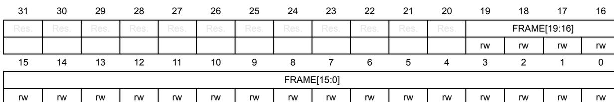
| 31 | 30 | 29 | 28 | 27 | 26 | 25 | 24 | 23 | 22 | 21 | 20 | 19 | 18 | 17 | 16 |
| Res. | Res. | Res. | Res. | Res. | Res. | Res. | Res. | Res. | Res. | Res. | Res. | FRAME[19:16] | |||
| rw | rw | rw | rw | ||||||||||||
| 15 | 14 | 13 | 12 | 11 | 10 | 9 | 8 | 7 | 6 | 5 | 4 | 3 | 2 | 1 | 0 |
| FRAME[15:0] | |||||||||||||||
| rw | rw | rw | rw | rw | rw | rw | rw | rw | rw | rw | rw | rw | rw | rw | rw |
Bits 31:20 Reserved, must be kept at reset value.
Bits 19:0 FRAME[19:0] : Frame numberCompare 1 value for the absolute frame counter.
18.5.18 GFXTIM absolute line counter compare 1 register (GFXTIM_ALCC1R)
Address offset: 0x070
Reset value: 0x0000 0000
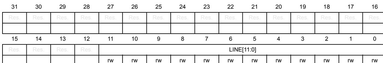
| 31 | 30 | 29 | 28 | 27 | 26 | 25 | 24 | 23 | 22 | 21 | 20 | 19 | 18 | 17 | 16 |
| Res. | Res. | Res. | Res. | Res. | Res. | Res. | Res. | Res. | Res. | Res. | Res. | Res. | Res. | Res. | Res. |
| 15 | 14 | 13 | 12 | 11 | 10 | 9 | 8 | 7 | 6 | 5 | 4 | 3 | 2 | 1 | 0 |
| Res. | Res. | Res. | Res. | LINE[11:0] | |||||||||||
| rw | rw | rw | rw | rw | rw | rw | rw | rw | rw | rw | rw | ||||
Bits 31:12 Reserved, must be kept at reset value.
Bits 11:0 LINE[11:0] : Line numberCompare value 1 for the absolute line counter.
18.5.19 GFXTIM absolute line counter compare 2 register (GFXTIM_ALCC2R)
Address offset: 0x074
Reset value: 0x0000 0000
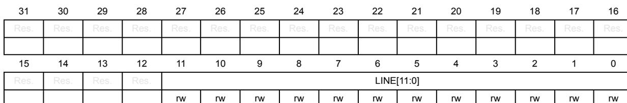
| 31 | 30 | 29 | 28 | 27 | 26 | 25 | 24 | 23 | 22 | 21 | 20 | 19 | 18 | 17 | 16 |
| Res. | Res. | Res. | Res. | Res. | Res. | Res. | Res. | Res. | Res. | Res. | Res. | Res. | Res. | Res. | Res. |
| 15 | 14 | 13 | 12 | 11 | 10 | 9 | 8 | 7 | 6 | 5 | 4 | 3 | 2 | 1 | 0 |
| Res. | Res. | Res. | Res. | LINE[11:0] | |||||||||||
| rw | rw | rw | rw | rw | rw | rw | rw | rw | rw | rw | rw | ||||
Bits 31:12 Reserved, must be kept at reset value.
Bits 11:0 LINE[11:0] : Line number
Compare value 2 for the absolute line counter.
18.5.20 GFXTIM relative frame counter 1 register (GFXTIM_RFC1R)
Address offset: 0x080
Reset value: 0x0000 0000
| 31 | 30 | 29 | 28 | 27 | 26 | 25 | 24 | 23 | 22 | 21 | 20 | 19 | 18 | 17 | 16 |
|---|---|---|---|---|---|---|---|---|---|---|---|---|---|---|---|
| Res. | Res. | Res. | Res. | Res. | Res. | Res. | Res. | Res. | Res. | Res. | Res. | Res. | Res. | Res. | Res. |
| 15 | 14 | 13 | 12 | 11 | 10 | 9 | 8 | 7 | 6 | 5 | 4 | 3 | 2 | 1 | 0 |
| Res. | Res. | Res. | Res. | FRAME[11:0] | |||||||||||
| r | r | r | r | r | r | r | r | r | r | r | r | ||||
Bits 31:12 Reserved, must be kept at reset value.
Bits 11:0 FRAME[11:0] : Frame number
Current value of the relative frame counter 1.
18.5.21 GFXTIM relative frame counter 1 reload register (GFXTIM_RFC1RR)
Address offset: 0x084
Reset value: 0x0000 0000
| 31 | 30 | 29 | 28 | 27 | 26 | 25 | 24 | 23 | 22 | 21 | 20 | 19 | 18 | 17 | 16 |
|---|---|---|---|---|---|---|---|---|---|---|---|---|---|---|---|
| Res. | Res. | Res. | Res. | Res. | Res. | Res. | Res. | Res. | Res. | Res. | Res. | Res. | Res. | Res. | Res. |
| 15 | 14 | 13 | 12 | 11 | 10 | 9 | 8 | 7 | 6 | 5 | 4 | 3 | 2 | 1 | 0 |
| Res. | Res. | Res. | Res. | FRAME[11:0] | |||||||||||
| rw | rw | rw | rw | rw | rw | rw | rw | rw | rw | rw | rw | ||||
Bits 31:12 Reserved, must be kept at reset value.
Bits 11:0 FRAME[11:0] : Frame reload value
Reload value for the relative frame counter 1.
18.5.22 GFXTIM relative frame counter 2 register (GFXTIM_RFC2R)
Address offset: 0x088
Reset value: 0x0000 0000
| 31 | 30 | 29 | 28 | 27 | 26 | 25 | 24 | 23 | 22 | 21 | 20 | 19 | 18 | 17 | 16 |
|---|---|---|---|---|---|---|---|---|---|---|---|---|---|---|---|
| Res. | Res. | Res. | Res. | Res. | Res. | Res. | Res. | Res. | Res. | Res. | Res. | Res. | Res. | Res. | Res. |
| 15 | 14 | 13 | 12 | 11 | 10 | 9 | 8 | 7 | 6 | 5 | 4 | 3 | 2 | 1 | 0 |
| Res. | Res. | Res. | Res. | FRAME[11:0] | |||||||||||
| r | r | r | r | r | r | r | r | r | r | r | r | ||||
Bits 31:12 Reserved, must be kept at reset value.
Bits 11:0 FRAME[11:0] : Frame number
Current value of the relative frame counter 2.
18.5.23 GFXTIM relative frame counter 2 reload register (GFXTIM_RFC2RR)
Address offset: 0x08C
Reset value: 0x0000 0000
| 31 | 30 | 29 | 28 | 27 | 26 | 25 | 24 | 23 | 22 | 21 | 20 | 19 | 18 | 17 | 16 |
|---|---|---|---|---|---|---|---|---|---|---|---|---|---|---|---|
| Res. | Res. | Res. | Res. | Res. | Res. | Res. | Res. | Res. | Res. | Res. | Res. | Res. | Res. | Res. | Res. |
| 15 | 14 | 13 | 12 | 11 | 10 | 9 | 8 | 7 | 6 | 5 | 4 | 3 | 2 | 1 | 0 |
| Res. | Res. | Res. | Res. | FRAME[11:0] | |||||||||||
| r | r | r | r | r | r | r | r | r | r | r | r | ||||
Bits 31:12 Reserved, must be kept at reset value.
Bits 11:0 FRAME[11:0] : Frame reload value
Reload value for the relative frame counter 2.
18.5.24 GFXTIM watchdog counter register (GFXTIM_WDGCR)
Address offset: 0x0A0
Reset value: 0x0000 0000
| 31 | 30 | 29 | 28 | 27 | 26 | 25 | 24 | 23 | 22 | 21 | 20 | 19 | 18 | 17 | 16 |
|---|---|---|---|---|---|---|---|---|---|---|---|---|---|---|---|
| Res. | Res. | Res. | Res. | Res. | Res. | Res. | Res. | Res. | Res. | Res. | Res. | Res. | Res. | Res. | Res. |
| 15 | 14 | 13 | 12 | 11 | 10 | 9 | 8 | 7 | 6 | 5 | 4 | 3 | 2 | 1 | 0 |
| VALUE[15:0] | |||||||||||||||
| r | r | r | r | r | r | r | r | r | r | r | r | r | r | r | r |
Bits 31:16 Reserved, must be kept at reset value.
Bits 15:0
VALUE[15:0]
: Value
Current value of the watchdog counter.
18.5.25 GFXTIM watchdog reload register (GFXTIM_WDGRR)
Address offset: 0x0A4
Reset value: 0x0000 0000
| 31 | 30 | 29 | 28 | 27 | 26 | 25 | 24 | 23 | 22 | 21 | 20 | 19 | 18 | 17 | 16 |
|---|---|---|---|---|---|---|---|---|---|---|---|---|---|---|---|
| Res. | Res. | Res. | Res. | Res. | Res. | Res. | Res. | Res. | Res. | Res. | Res. | Res. | Res. | Res. | Res. |
| 15 | 14 | 13 | 12 | 11 | 10 | 9 | 8 | 7 | 6 | 5 | 4 | 3 | 2 | 1 | 0 |
| RELOAD[15:0] | |||||||||||||||
| rw | rw | rw | rw | rw | rw | rw | rw | rw | rw | rw | rw | rw | rw | rw | rw |
Bits 31:16 Reserved, must be kept at reset value.
Bits 15:0
RELOAD[15:0]
: Reload value
Reload value of the watchdog counter.
18.5.26 GFXTIM watchdog pre-alarm register (GFXTIM_WDGPAR)
Address offset: 0x0A8
Reset value: 0x0000 0000
| 31 | 30 | 29 | 28 | 27 | 26 | 25 | 24 | 23 | 22 | 21 | 20 | 19 | 18 | 17 | 16 |
|---|---|---|---|---|---|---|---|---|---|---|---|---|---|---|---|
| Res. | Res. | Res. | Res. | Res. | Res. | Res. | Res. | Res. | Res. | Res. | Res. | Res. | Res. | Res. | Res. |
| 15 | 14 | 13 | 12 | 11 | 10 | 9 | 8 | 7 | 6 | 5 | 4 | 3 | 2 | 1 | 0 |
| PREALARM[15:0] | |||||||||||||||
| rw | rw | rw | rw | rw | rw | rw | rw | rw | rw | rw | rw | rw | rw | rw | rw |
Bits 31:16 Reserved, must be kept at reset value.
Bits 15:0
PREALARM[15:0]
: Pre-alarm value
Pre-alarm value of the watchdog counter.
18.5.27 GFXTIM register map
Table 141. GFXTIM register map and reset values
| Offset | Register name | 31 | 30 | 29 | 28 | 27 | 26 | 25 | 24 | 23 | 22 | 21 | 20 | 19 | 18 | 17 | 16 | 15 | 14 | 13 | 12 | 11 | 10 | 9 | 8 | 7 | 6 | 5 | 4 | 3 | 2 | 1 | 0 |
|---|---|---|---|---|---|---|---|---|---|---|---|---|---|---|---|---|---|---|---|---|---|---|---|---|---|---|---|---|---|---|---|---|---|
| 0x000 | GFXTIM_CR | Res. | LCCOE | FCCOE | Res. | SYNCS [1:0] | Res. | Res. | TES [1:0] | ||||||||||||||||||||||||
| Reset value | 0 | 0 | 0 | 0 | 0 | 0 | |||||||||||||||||||||||||||
| 0x004 | GFXTIM_CGCR | Res. | FCCHRS [2:0] | Res. | FCCFR | Res. | FCCCS [2:0] | Res. | FCS [2:0] | Res. | LCCHRS [2:0] | Res. | LCCFR | Res. | TEPOL | LCCCS | LCS[2:0] | ||||||||||||||||
| Reset value | 0 | 0 | 0 | 0 | 0 | 0 | 0 | 0 | 0 | 0 | 0 | 0 | 0 | 0 | 0 | 0 | 0 | 0 | 0 | ||||||||||||||
Table 141. GFXTIM register map and reset values (continued)
| Offset | Register name | 31 | 30 | 29 | 28 | 27 | 26 | 25 | 24 | 23 | 22 | 21 | 20 | 19 | 18 | 17 | 16 | 15 | 14 | 13 | 12 | 11 | 10 | 9 | 8 | 7 | 6 | 5 | 4 | 3 | 2 | 1 | 0 | |
|---|---|---|---|---|---|---|---|---|---|---|---|---|---|---|---|---|---|---|---|---|---|---|---|---|---|---|---|---|---|---|---|---|---|---|
| 0x008 | GFXTIM_TCR | Res | Res | Res | Res | Res | Res | Res | Res | Res | o | o | o | Res | o | o | Res | Res | Res | Res | Res | Res | Res | Res | Res | Res | Res | o | o | Res | Res | Res | o | o |
| Reset value | ||||||||||||||||||||||||||||||||||
| 0x00C | GFXTIM_TDR | Res | Res | Res | Res | Res | Res | Res | Res | Res | Res | Res | o | Res | Res | Res | o | Res | Res | Res | Res | Res | Res | Res | Res | Res | Res | Res | o | o | Res | Res | o | o |
| Reset value | ||||||||||||||||||||||||||||||||||
| 0x010 | GFXTIM_EVCR | Res | Res | Res | Res | Res | Res | Res | Res | Res | Res | Res | Res | Res | Res | Res | Res | Res | Res | Res | Res | Res | Res | Res | Res | Res | Res | Res | Res | o | o | o | o | o |
| Reset value | ||||||||||||||||||||||||||||||||||
| 0x014 | GFXTIM_EVSR | Res | FES4[2:0] | Res | LES4[2:0] | Res | FES3[2:0] | Res | LES3[2:0] | Res | FES2[2:0] | Res | LES2[2:0] | Res | FES1[2:0] | Res | LES1[2:0] | Res | Res | Res | Res | Res | Res | Res | Res | Res | Res | Res | Res | Res | Res | Res | Res | |
| Reset value | 0 0 0 | 0 0 0 | 0 0 0 | 0 0 0 | 0 0 0 | 0 0 0 | 0 0 0 | 0 0 0 | ||||||||||||||||||||||||||
| 0x018-0x01C | Reserved | Reserved | ||||||||||||||||||||||||||||||||
| 0x020 | GFXTIM_WDGTCR | Res | Res | Res | Res | Res | Res | Res | Res | Res | Res | Res | Res | Res | Res | Res | o | Res | Res | Res | Res | WDGCS[3:0] | Res | Res | Res | Res | o | o | Res | o | o | o | o | |
| Reset value | ||||||||||||||||||||||||||||||||||
| 0x024-0x02C | Reserved | Reserved | ||||||||||||||||||||||||||||||||
| 0x030 | GFXTIM_ISR | Res | Res | Res | Res | Res | Res | o | o | Res | Res | Res | Res | o | o | o | o | Res | Res | o | o | Res | Res | o | o | Res | Res | Res | o | o | o | o | o | o |
| Reset value | ||||||||||||||||||||||||||||||||||
| 0x034 | GFXTIM_ICR | Res | Res | Res | Res | Res | Res | o | o | Res | Res | Res | Res | o | o | o | o | Res | Res | o | o | Res | Res | o | o | Res | Res | Res | o | o | o | o | o | o |
| Reset value | ||||||||||||||||||||||||||||||||||
| 0x038 | GFXTIM_IER | Res | Res | Res | Res | Res | Res | o | o | Res | Res | Res | Res | o | o | o | o | Res | Res | o | o | Res | Res | o | o | Res | Res | Res | o | o | o | o | o | o |
| Reset value | ||||||||||||||||||||||||||||||||||
| 0x03C | GFXTIM_TSR | Res | Res | Res | Res | Res | Res | Res | Res | Res | Res | Res | o | Res | Res | Res | o | Res | Res | o | o | Res | Res | o | o | Res | Res | Res | o | o | o | o | o | o |
| Reset value | ||||||||||||||||||||||||||||||||||
| 0x040 | GFXTIM_LCCRR | Res | Res | Res | Res | Res | Res | Res | Res | Res | Res | Res | Res | Res | Res | Res | Res | Res | Res | Res | Res | Res | Res | Res | Res | Res | Res | Res | Res | Res | Res | Res | Res | |
| Reset value | ||||||||||||||||||||||||||||||||||
| 0x044 | GFXTIM_FCCRR | Res | Res | Res | Res | Res | Res | Res | Res | Res | Res | Res | Res | Res | Res | Res | Res | Res | Res | Res | Res | Res | Res | Res | Res | Res | Res | Res | Res | Res | Res | Res | Res | |
| Reset value | ||||||||||||||||||||||||||||||||||
| 0x048-0x04C | Reserved | Reserved | ||||||||||||||||||||||||||||||||
| 0x050 | GFXTIM_ATR | Res | Res | Res | Res | Res | Res | Res | Res | Res | Res | Res | Res | Res | Res | Res | Res | Res | Res | Res | Res | Res | Res | Res | Res | Res | Res | Res | Res | Res | Res | Res | Res | |
| Reset value | 0 | 0 | 0 | 0 | 0 | 0 | 0 | 0 | 0 | 0 | 0 | 0 | 0 | 0 | 0 | 0 | 0 | 0 | 0 | 0 | 0 | 0 | 0 | 0 | 0 | 0 | 0 | 0 | 0 | 0 | 0 | 0 | ||
| 0x054 | GFXTIM_AFCR | Res | Res | Res | Res | Res | Res | Res | Res | Res | Res | Res | Res | Res | Res | Res | Res | Res | Res | Res | Res | Res | Res | Res | Res | Res | Res | Res | Res | Res | Res | Res | Res | |
| Reset value | ||||||||||||||||||||||||||||||||||
| 0x058 | GFXTIM_ALCR | Res | Res | Res | Res | Res | Res | Res | Res | Res | Res | Res | Res | Res | Res | Res | Res | Res | Res | Res | Res | Res | Res | Res | Res | Res | Res | Res | Res | Res | Res | Res | Res | |
| Reset value | ||||||||||||||||||||||||||||||||||
| 0x05C | Reserved | Reserved | ||||||||||||||||||||||||||||||||
Table 141. GFXTIM register map and reset values (continued)
| Offset | Register name | 31 | 30 | 29 | 28 | 27 | 26 | 25 | 24 | 23 | 22 | 21 | 20 | 19 | 18 | 17 | 16 | 15 | 14 | 13 | 12 | 11 | 10 | 9 | 8 | 7 | 6 | 5 | 4 | 3 | 2 | 1 | 0 |
|---|---|---|---|---|---|---|---|---|---|---|---|---|---|---|---|---|---|---|---|---|---|---|---|---|---|---|---|---|---|---|---|---|---|
| 0x060 | GFXTIM_AFCC1R | Res | Res | Res | Res | Res | Res | Res | Res | Res | Res | Res | Res | FRAME[19:0] | |||||||||||||||||||
| Reset value | 0 | 0 | 0 | 0 | 0 | 0 | 0 | 0 | 0 | 0 | 0 | 0 | 0 | 0 | 0 | 0 | 0 | 0 | 0 | 0 | |||||||||||||
| 0x064-0x06C | Reserved | Reserved | |||||||||||||||||||||||||||||||
| 0x070 | GFXTIM_ALCC1R | Res | Res | Res | Res | Res | Res | Res | Res | Res | Res | Res | Res | Res | Res | Res | Res | Res | Res | Res | Res | LINE[11:0] | |||||||||||
| Reset value | 0 | 0 | 0 | 0 | 0 | 0 | 0 | 0 | 0 | 0 | 0 | ||||||||||||||||||||||
| 0x074 | GFXTIM_ALCC2R | Res | Res | Res | Res | Res | Res | Res | Res | Res | Res | Res | Res | Res | Res | Res | Res | Res | Res | Res | Res | LINE[11:0] | |||||||||||
| Reset value | 0 | 0 | 0 | 0 | 0 | 0 | 0 | 0 | 0 | 0 | 0 | ||||||||||||||||||||||
| 0x078-0x07C | Reserved | Reserved | |||||||||||||||||||||||||||||||
| 0x080 | GFXTIM_RFC1R | Res | Res | Res | Res | Res | Res | Res | Res | Res | Res | Res | Res | Res | Res | Res | Res | Res | Res | Res | Res | FRAME[11:0] | |||||||||||
| Reset value | 0 | 0 | 0 | 0 | 0 | 0 | 0 | 0 | 0 | 0 | 0 | ||||||||||||||||||||||
| 0x084 | GFXTIM_RFC1RR | Res | Res | Res | Res | Res | Res | Res | Res | Res | Res | Res | Res | Res | Res | Res | Res | Res | Res | Res | Res | FRAME[11:0] | |||||||||||
| Reset value | 0 | 0 | 0 | 0 | 0 | 0 | 0 | 0 | 0 | 0 | 0 | ||||||||||||||||||||||
| 0x088 | GFXTIM_RFC2R | Res | Res | Res | Res | Res | Res | Res | Res | Res | Res | Res | Res | Res | Res | Res | Res | Res | Res | Res | Res | FRAME[11:0] | |||||||||||
| Reset value | 0 | 0 | 0 | 0 | 0 | 0 | 0 | 0 | 0 | 0 | 0 | ||||||||||||||||||||||
| 0x08C | GFXTIM_RFC2RR | Res | Res | Res | Res | Res | Res | Res | Res | Res | Res | Res | Res | Res | Res | Res | Res | Res | Res | Res | Res | FRAME[11:0] | |||||||||||
| Reset value | 0 | 0 | 0 | 0 | 0 | 0 | 0 | 0 | 0 | 0 | 0 | ||||||||||||||||||||||
| 0x090-0x09C | Reserved | Reserved | |||||||||||||||||||||||||||||||
| 0x0A0 | GFXTIM_WDGCR | Res | Res | Res | Res | Res | Res | Res | Res | Res | Res | Res | Res | Res | Res | Res | Res | Res | Res | Res | Res | VALUE[15:0] | |||||||||||
| Reset value | 0 | 0 | 0 | 0 | 0 | 0 | 0 | 0 | 0 | 0 | 0 | ||||||||||||||||||||||
| 0x0A4 | GFXTIM_WDGRR | Res | Res | Res | Res | Res | Res | Res | Res | Res | Res | Res | Res | Res | Res | Res | Res | Res | Res | Res | Res | RELOAD[15:0] | |||||||||||
| Reset value | 0 | 0 | 0 | 0 | 0 | 0 | 0 | 0 | 0 | 0 | 0 | ||||||||||||||||||||||
| 0x0A8 | GFXTIM_WDGPAR | Res | Res | Res | Res | Res | Res | Res | Res | Res | Res | Res | Res | Res | Res | Res | Res | Res | Res | Res | Res | PREALARM[15:0] | |||||||||||
| Reset value | 0 | 0 | 0 | 0 | 0 | 0 | 0 | 0 | 0 | 0 | 0 | ||||||||||||||||||||||
Refer to Section 2.3: Memory organization for the register boundary addresses.