17. Texture cache (ICACHE)
17.1 ICACHE introduction
The texture cache (ICACHE) is introduced on the AXI read-only texture port of the GPU to improve performance when reading texture data from internal and external memories.
The texture cache is an assembly of ICACHE (a peripheral with AHB ports) and an AXI-to-AHB bus bridge plugged on ICACHE AHB slave port, providing an AXI interface on the texture cache slave port.
The following sections only describe the AHB ICACHE peripheral itself.
Some specific features, like hit-under-miss, and critical-word-first refill policy, result in close to zero-wait-state performance in most use cases.
17.2 ICACHE main features
The main features of ICACHE are listed below:
- • Bus interface
- – One 64-bit AHB slave port, the read port (input from GPU texture read interface)
- – One 64-bit AHB master port: master1 port (output to texture bus of main AXI/AHB bus matrix)
- – One 32-bit AHB slave port for control (input from AHB peripherals interconnect, for ICACHE registers access)
- • Cache access
- – 0 wait-state on hits
- – Hit-under-miss capability: ability to serve processor requests (access to cached data) during an ongoing line refill due to a previous cache miss
- – Optimal cache line refill thanks to WRAPw bursts of the size of the cache line (32-bit word size, w , aligned on cache line size)
- – n-way set-associative default configuration with possibility to configure as 1-way, means direct mapped cache, for applications needing very-low-power consumption profile
- • Replacement and refill
- – pLRU-t (pseudo-least-recently-used, based on binary tree) replacement policy, algorithm with best complexity/performance balance
- – Critical-word-first refill policy, minimizing processor stalls
- • Performance counters
The ICACHE implements two performance counters:
- – Hit monitor counter (32-bit)
- – Miss monitor counter (16-bit)
- • Error management
- – Possibility to detect an unexpected cacheable write access, to flag an error, and optionally, to raise an interrupt
- • Maintenance operation
- – Cache invalidate: full cache invalidation, fast command, noninterruptible
17.3 ICACHE implementation
Table 131. ICACHE features| Feature | ICACHE |
|---|---|
| Number of ways | 4 |
| Cache size | 16 Kbytes |
| Cache line width | 32 bytes |
| Number of regions to remap | 0 |
| Data size of AHB slave interface | 64 bits |
| Data size of AHB fast master1 interface | 64 bits |
| Data size of AHB slow master2 interface | 0 |
17.4 ICACHE functional description
The purpose of the texture cache is to cache GPU read accesses to texture data. As such, the ICACHE manages only cacheable read transactions, and does not manage cacheable write transactions.
The noncacheable transactions (both read and write) bypass the ICACHE.
For the error management purpose, if a write cacheable transaction is presented (this happens only in case of bad software programming), the ICACHE sets an error flag and, if enabled, raises an interrupt to the processor.
17.4.1 ICACHE block diagram
Figure 138. ICACHE block diagram
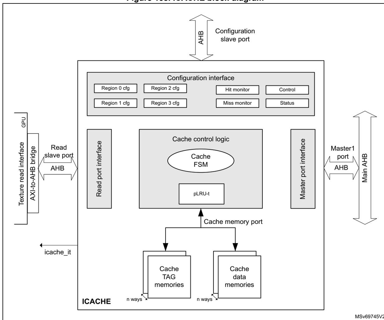
The diagram illustrates the internal architecture of the ICACHE block. At the top, an external 'Configuration slave port' connects via an 'AHB' interface to the 'Configuration interface'. This interface contains four configuration registers: 'Region 0 cfg', 'Region 1 cfg', 'Region 2 cfg', and 'Region 3 cfg', as well as 'Hit monitor', 'Miss monitor', 'Control', and 'Status' blocks. On the left, a 'Texture read interface' from a 'GPU' connects through an 'AXI-to-AHB bridge' to a 'Read slave port' on the 'Read port interface'. An 'icache_it' signal is also shown on this side. The central 'Cache control logic' block contains a 'Cache FSM' and a 'pLRU-t' unit. It is connected to the 'Read port interface', the 'Master port interface', and the 'Cache memory port'. The 'Master port interface' connects to 'Master1 port' on the 'Main AHB'. The 'Cache memory port' leads to 'Cache TAG memories' and 'Cache data memories', both of which are organized into 'n ways'. The entire internal structure is labeled 'ICACHE' at the bottom left. A reference code 'MSv69745V2' is located at the bottom right of the diagram.
17.4.2 ICACHE reset and clocks
The ICACHE is clocked on the texture AHB bus clock.
When the ICACHE reset signal is released, a cache invalidate procedure is automatically launched, making the ICACHE busy (ICACHE_SR = 0x0000 0001).
When this procedure is finished:
- • the ICACHE is invalidated: “cold cache”, with all cache line valid bits = 0 (ICACHE must be filled up)
- • ICACHE_SR = 0x0000 0002 (reflecting the cache is no longer busy)
- • the ICACHE is disabled: the EN bit in ICACHE_CR holds its reset state (= 0).
Note: When disabled, the ICACHE is bypassed: slave input requests are forwarded to the master port.
17.4.3 ICACHE TAG memory
The ICACHE TAG memory contains:
- • address tags indicating which data are contained in the cache data memories
- • validity bits
There is one valid bit per cache line (per way).
The valid bit is set when a cache line is refilled (after a miss).
Valid bits are reset in any of the below cases:
- • after the ICACHE reset is released
- • when the cache is disabled, by setting EN = 0 in ICACHE_CR (by software)
- • when executing an ICACHE invalidate command, by setting CACHEINV = 1 in ICACHE_CR (by software)
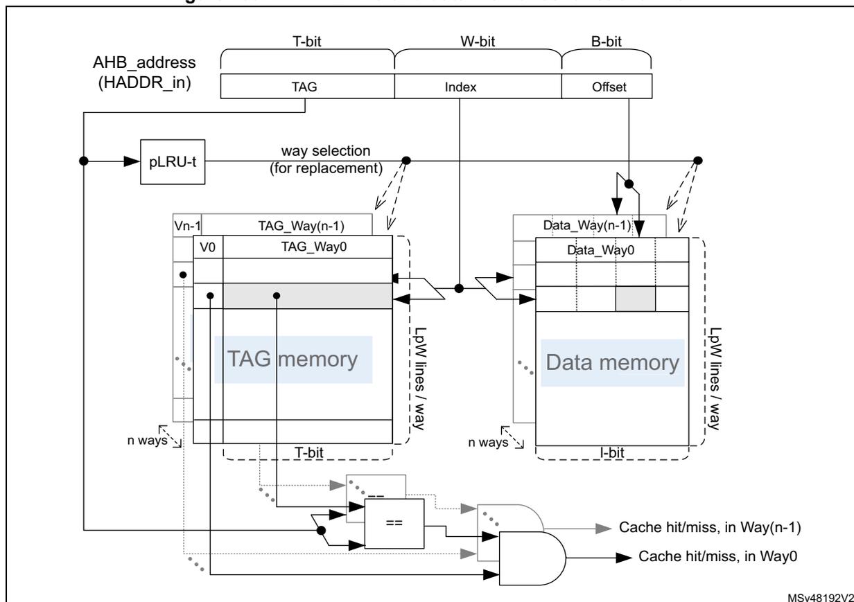
When a cacheable transaction is received at the execution input port, its AHB address (HADDR_in) is split into the following fields (see Table 132 for B and W definitions):
- • HADDR_in[B-1:0]: address byte offset, indicates which byte to select inside a cache line.
- • HADDR_in[B+W-1:B]: address way index, indicates which cache line to select inside each way.
- • HADDR_in[31:B+W]: tag address, to be compared to the TAG memory address to check if the requested data is already available (meaning valid) inside the ICACHE.
The following table gives a summary of the ICACHE main parameters for TAG memory dimensioning. Figure 139 shows the functional view of TAG and data memories, for an n-way set associative ICACHE.
Table 132. TAG memory dimensioning parameters for n-way set associative operating mode (default)
| Parameter | Value | Example |
|---|---|---|
| Cache size | S Kbytes = s bytes (s = 1024 x S) | 8 Kbytes = 8192 bytes |
| Cache number of ways | n | 2 |
| Cache line size | L-byte = l-bit (l = 8 x L) | 16-byte = 128-bit |
| Number of cache lines | LpW = s / (n x L) lines / way | 256 lines / way |
| Address byte offset size | B = log 2 (L) bit | 4-bit |
| Address way index size | W = log 2 (LpW) bit | 8-bit |
| TAG address size | T = (32 - W - B) bit | 20-bit |
Figure 139. ICACHE TAG and data memories functional view
MSv48192V2
17.4.4 Direct-mapped ICACHE (1-way cache)
The default configuration (at reset) is an n-way set associative cache (WAYSEL = 1 in ICACHE_CR), but the user can configure the ICACHE as direct mapped by writing WAYSEL = 0 (only possible when the cache is disabled, EN = 0 in ICACHE_CR).
The following table gives a summary of ICACHE main parameters for TAG memory when the direct-mapped cache operating mode is selected.
Table 133. TAG memory dimensioning parameters for direct-mapped cache mode
| Parameter | Value | Example |
|---|---|---|
| Cache size | S Kbytes = s bytes (s = 1024 x S) | 8 Kbytes = 8192 bytes |
| Cache number of ways | 1 | 1 |
| Cache line size | L-byte = l-bit (l = 8 x L) | 16-byte = 128-bit |
| Number of cache lines | LpW = s / L lines | 512 lines |
| Address byte offset size | B = log 2 (L) bit | 4-bit |
| Address way index size | W = log 2 (LpW) bit | 9-bit |
| TAG address size | T = (32 - W - B) bit | 19-bit |
All cache operations (such as read, refill, invalidation) remain the same in the direct-mapped configuration. The only difference is the absence of a replacement algorithm in case of line eviction (as explained in Section 17.4.7 ): only one way (the unique one) is possible for any data refill.
17.4.5 ICACHE enable
To activate the ICACHE, the EN bit in ICACHE_CR must be set to 1.
When the ICACHE is disabled, it is bypassed and all transactions are copied from the slave to the master port in the same clock cycle.
It is recommended to initialize or modify the main memory content (region to be later cached) with the ICACHE disabled, and to enable the ICACHE only when this region remains unchanged (an enabled ICACHE detects cacheable write transactions as errors).
To ensure performance determinism, it is recommended to wait for the end of a potential cache invalidate procedure before enabling the ICACHE. This procedure occurs when the hardware reset signal is released, when CACHEINV is set, or when EN is cleared in ICACHE_CR. During the procedure, BUSYF is set in ICACHE_SR, and once finished, BUSYF is cleared and BSYENDF is set in the same register (raising the ICACHE interrupt if enabled on such a busy end condition).
The software must test BUSYF and/or BSYENDF values before enabling the ICACHE. Else, if the ICACHE is enabled before the end of an invalidate procedure, any cache access (while BUSYF = 1) is treated as noncacheable, and its performance depends on the main memory access time.
The ICACHE is, by default, disabled at boot.
17.4.6 Cacheable and noncacheable traffic
The ICACHE is placed on the GPU texture bus, and thus caches all internal and external memory regions (ranging from address 0x0000 0000 to 0x3FFF FFFF, respectively 0x6000 0000 to 0x9FFF FFFF, of the memory map).
An incoming memory request to the ICACHE is defined as cacheable according to its AHB transaction memory lookup attribute, as shown in Table 134 . This AHB attribute depends on the GPU setting for the addressed region.
Table 134. ICACHE cacheability for AHB transaction
| AHB lookup attribute | Cacheability |
|---|---|
| 1 | Cacheable |
| 0 | Noncacheable |
In the case of a noncacheable access (read or write), the ICACHE is bypassed. The AHB transaction is propagated unchanged to the master output port.
The bypass does not increase the latency of the access to the targeted memory.
In the case of a cacheable access, the ICACHE behaves as explained in Section 17.4.7 .
17.4.7 Cacheable accesses
When the ICACHE receives a cacheable transaction from the GPU, it checks if the address requested is present in its TAG memory, and if the corresponding cache line is valid.
There are then three alternatives:
- • The address is present inside the TAG memory, the cache line is valid: cache hit , the data is read from the cache and provided to the processor in the same cycle.
- • The address is not present in the TAG memory: cache miss , the data is read from the main memory and provided to the processor, and a cache line refill is performed.
The critical-word-first policy ensures minimum wait cycles for the processor, since read data can be provided while the cache still performs a cache line refill (associated latency is the latency of fetching one word from the main memory).
The burst generated on the ICACHE master bus is WRAPw (w being the cache line width, in words).
The AHB transaction attributes are also propagated to the main AHB bus matrix on the master port.
- • The address is not present in TAG memory, but belongs to the refill burst from the main memory currently ongoing: cache hit (hit-under-miss feature).
This happens during cache-line refill. The ICACHE can provide the requested data as soon as data are available at its master interface, thus avoiding a miss (fetching data from the main memory).
In the case of cache refill (due to cache miss), the ICACHE selects which cache line is written with the refill data:
- • In direct map (1-way) mode, only one line can be used to store the refill data: the line pointed by the index of the input address.
- • In n-way set associative mode, one line among n can be used (the line pointed by the address index, in each of the n ways). The way selection is based on a pLRU-t replacement algorithm that points, for each index, on the way candidate for the next refill.
If the cache line where the refill data must be written is already valid, the targeted cache line must be invalidated first. This is true whatever the direct map or n-way set associative cache mode.
17.4.8 ICACHE maintenance
The software can invalidate the whole content of the ICACHE by programming CACHEINV in the ICACHE_CR register.
When CACHEINV = 1, the ICACHE control logic sets the BUSYF flag in ICACHE_SR and launches the invalidate cache operation, resetting each TAG valid bit to 0 (one valid bit per cache line). CACHEINV is automatically cleared.
Once the invalidate operation is finished (all valid bits reset to 0), the ICACHE automatically clears BUSYF, and sets BSYENDF in the ICACHE_SR register.
If enabled on this flag condition (BSYENDIE = 1 in ICACHE_IER), the ICACHE interrupt is raised. Then, the (empty) cache is available again.
17.4.9 ICACHE performance monitoring
The ICACHE provides the following monitors for performance analysis:
- • The 32-bit hit monitor counts the cacheable AHB-transactions on the slave cache port that hits the ICACHE content.
It also takes into account all accesses whose address is present in the TAG memory or in the refill buffer (due to a previous miss, and whose data is coming, or is soon to come, from the cache master port) (see Section 17.4.7 ).
- • The 16-bit miss monitor counts the cacheable AHB-transactions on the slave cache port that misses the ICACHE content.
It also takes into account all accesses whose address is not present neither in the TAG memory nor in the refill buffer.
Upon reaching their maximum values, these monitors do not wrap over.
Hit and miss monitors can be enabled and reset by software allowing the analysis of specific pieces of code.
The software can perform the following tasks:
- • Enable/stop the hit monitor through HITMEN in ICACHE_CR.
- • Reset the hit monitor by setting HITMRST in ICACHE_CR.
- • Enable/stop the miss monitor through MISSMEN in ICACHE_CR.
- • Reset the miss monitor by setting MISSMRST in ICACHE_CR.
To reduce power consumption, these monitors are disabled (stopped) by default.
17.4.10 ICACHE boot
The ICACHE is disabled (EN = 0 in ICACHE_CR) at boot.
Once the boot is finished, the ICACHE can be enabled (software setting EN = 1 in ICACHE_CR).
17.5 ICACHE low-power modes
At device level, using the ICACHE reduces the power consumption by reading textures from the internal ICACHE most of the time, rather than from the bigger and then more power consuming main memories. This reduction is even higher if the cached main memories are external.
Applications with lower performance profile (in terms of hit ratio) and stringent power consumption constraints may benefit from the lower power consumption of an ICACHE configured as direct mapped. This single-way cache configuration is obtained by programming WAYSEL = 0 in ICACHE_CR (see Figure 139 ). The power consumption is reduced by accessing, for each request, only the necessary cut of TAG and data memories. The cache effect still improves memory access performance, even if for most texture accesses, it is less efficient than with an n-way set associative cache mode.
17.6 ICACHE error management and interrupts
If an unsupported cacheable write request is detected (functional error), the ICACHE generates an error by setting the ERRF flag in ICACHE_SR. An interrupt is generated if the corresponding interrupt enable bit is set (ERRIE = 1 in ICACHE_IER).
The other possible interrupt generation is at the end of a cache invalidation operation. When the cache-busy state is finished, the ICACHE sets the BSYENDF flag in ICACHE_SR. An interrupt is generated if the corresponding interrupt enable bit is set (BSYENDIE = 1 in ICACHE_IER).
All ICACHE interrupt sources raise the same and unique interrupt signal, icache_it, and then use the same interrupt vector.
Table 135. ICACHE interrupts
| Interrupt vector | Interrupt event | Event flag | Enable control bit | Interrupt clear method |
|---|---|---|---|---|
| ICACHE | Functional error | ERRF in ICACHE_SR | ERRIE in ICACHE_IER | Set CERRF to 1 in ICACHE_FCR |
| End of busy state (invalidate finished) | BSYENDF in ICACHE_SR | BSYENDIE in ICACHE_IER | Set CBSYENDF to 1 in ICACHE_FCR |
The ICACHE also propagates all AHB bus errors (such as address decoding issues) from the master1 port back to the slave read port.
17.7 ICACHE registers
17.7.1 ICACHE control register (ICACHE_CR)
Address offset: 0x000
Reset value: 0x0000 0004
| 31 | 30 | 29 | 28 | 27 | 26 | 25 | 24 | 23 | 22 | 21 | 20 | 19 | 18 | 17 | 16 |
|---|---|---|---|---|---|---|---|---|---|---|---|---|---|---|---|
| Res. | Res. | Res. | Res. | Res. | Res. | Res. | Res. | Res. | Res. | Res. | Res. | MISS MRST | HITM RST | MISS MEN | HITM EN |
| rw | rw | rw | rw | ||||||||||||
| 15 | 14 | 13 | 12 | 11 | 10 | 9 | 8 | 7 | 6 | 5 | 4 | 3 | 2 | 1 | 0 |
| Res. | Res. | Res. | Res. | Res. | Res. | Res. | Res. | Res. | Res. | Res. | Res. | Res. | WAY SEL | CACHE INV | EN |
| rw | w | rw |
Bits 31:20 Reserved, must be kept at reset value.
Bit 19 MISSMRST : miss monitor reset
0: release the cache miss monitor reset (needed to enable the counting)
1: reset cache miss monitor
Bit 18 HITMRST : hit monitor reset
0: release the cache miss monitor reset (needed to enable the counting)
1: reset cache hit monitor
Bit 17 MISSMEN : miss monitor enable
0: cache miss monitor switched off. Stopping the monitor does not reset it.
1: cache miss monitor enabled
Bit 16 HITMEN : hit monitor enable
0: cache hit monitor switched off. Stopping the monitor does not reset it.
1: cache hit monitor enabled
Bits 15:3 Reserved, must be kept at reset value.
Bit 2 WAYSEL : cache associativity mode selection
This bit allows user to choose ICACHE set-associativity. It can be written by software only when cache is disabled (EN = 0).
0: direct mapped cache (1-way cache)
1: n-way set associative cache (reset value)
Bit 1 CACHEINV : cache invalidation
Set by software and cleared by hardware when the BUSYF flag is set (during cache maintenance operation). Writing 0 has no effect.
0: no effect
1: invalidate entire cache (all cache lines valid bit = 0)
Bit 0 EN : enable
0: cache disabled
1: cache enabled
17.7.2 ICACHE status register (ICACHE_SR)
Address offset: 0x004
Reset value: 0x0000 0001
| 31 | 30 | 29 | 28 | 27 | 26 | 25 | 24 | 23 | 22 | 21 | 20 | 19 | 18 | 17 | 16 |
|---|---|---|---|---|---|---|---|---|---|---|---|---|---|---|---|
| Res. | Res. | Res. | Res. | Res. | Res. | Res. | Res. | Res. | Res. | Res. | Res. | Res. | Res. | Res. | Res. |
| 15 | 14 | 13 | 12 | 11 | 10 | 9 | 8 | 7 | 6 | 5 | 4 | 3 | 2 | 1 | 0 |
| Res. | Res. | Res. | Res. | Res. | Res. | Res. | Res. | Res. | Res. | Res. | Res. | Res. | ERRF | BSYEN DF | BUSYF |
| r | r | r |
Bits 31:3 Reserved, must be kept at reset value.
Bit 2 ERRF : cache error flag
0: no error
1: an error occurred during the operation (cacheable write)
Bit 1 BSYENDF : busy end flag
0: cache busy
1: full invalidate CACHEINV operation finished
Bit 0 BUSYF : busy flag
0: cache not busy on a CACHEINV operation
1: cache executing a full invalidate CACHEINV operation
17.7.3 ICACHE interrupt enable register (ICACHE_IER)
Address offset: 0x008
Reset value: 0x0000 0000
| 31 | 30 | 29 | 28 | 27 | 26 | 25 | 24 | 23 | 22 | 21 | 20 | 19 | 18 | 17 | 16 |
|---|---|---|---|---|---|---|---|---|---|---|---|---|---|---|---|
| Res. | Res. | Res. | Res. | Res. | Res. | Res. | Res. | Res. | Res. | Res. | Res. | Res. | Res. | Res. | Res. |
| 15 | 14 | 13 | 12 | 11 | 10 | 9 | 8 | 7 | 6 | 5 | 4 | 3 | 2 | 1 | 0 |
| Res. | Res. | Res. | Res. | Res. | Res. | Res. | Res. | Res. | Res. | Res. | Res. | Res. | ERRIE | BSYENDIE | Res. |
| rw | rw |
Bits 31:3 Reserved, must be kept at reset value.
Bit 2 ERRIE : interrupt enable on cache error
Set by software to enable an interrupt generation in case of cache functional error (cacheable write access)
0: interrupt disabled on error
1: interrupt enabled on error
Bit 1 BSYENDIE : interrupt enable on busy end
Set by software to enable an interrupt generation at the end of a cache invalidate operation.
0: interrupt disabled on busy end
1: interrupt enabled on busy end
Bit 0 Reserved, must be kept at reset value.
17.7.4 ICACHE flag clear register (ICACHE_FCR)
Address offset: 0x00C
Reset value: 0x0000 0000
| 31 | 30 | 29 | 28 | 27 | 26 | 25 | 24 | 23 | 22 | 21 | 20 | 19 | 18 | 17 | 16 |
|---|---|---|---|---|---|---|---|---|---|---|---|---|---|---|---|
| Res. | Res. | Res. | Res. | Res. | Res. | Res. | Res. | Res. | Res. | Res. | Res. | Res. | Res. | Res. | Res. |
| 15 | 14 | 13 | 12 | 11 | 10 | 9 | 8 | 7 | 6 | 5 | 4 | 3 | 2 | 1 | 0 |
| Res. | Res. | Res. | Res. | Res. | Res. | Res. | Res. | Res. | Res. | Res. | Res. | Res. | CERRF | CBSYENDF | Res. |
| w | w |
Bits 31:3 Reserved, must be kept at reset value.
Bit 2 CERRF : clear cache error flag
Set by software.
0: no effect
1: clears ERRF flag in ICACHE_SR
Bit 1 CBSYENDF : clear busy end flag
Set by software.
0: no effect
1: clears BSYENDF flag in ICACHE_SR.
Bit 0 Reserved, must be kept at reset value.
17.7.5 ICACHE hit monitor register (ICACHE_HMONR)
Address offset: 0x010
Reset value: 0x0000 0000
| 31 | 30 | 29 | 28 | 27 | 26 | 25 | 24 | 23 | 22 | 21 | 20 | 19 | 18 | 17 | 16 |
|---|---|---|---|---|---|---|---|---|---|---|---|---|---|---|---|
| HITMON[31:16] | |||||||||||||||
| r | r | r | r | r | r | r | r | r | r | r | r | r | r | r | r |
| 15 | 14 | 13 | 12 | 11 | 10 | 9 | 8 | 7 | 6 | 5 | 4 | 3 | 2 | 1 | 0 |
| HITMON[15:0] | |||||||||||||||
| r | r | r | r | r | r | r | r | r | r | r | r | r | r | r | r |
Bits 31:0 HITMON[31:0] : cache hit monitor counter
17.7.6 ICACHE miss monitor register (ICACHE_MMONR)
Address offset: 0x014
Reset value: 0x0000 0000
| 31 | 30 | 29 | 28 | 27 | 26 | 25 | 24 | 23 | 22 | 21 | 20 | 19 | 18 | 17 | 16 |
|---|---|---|---|---|---|---|---|---|---|---|---|---|---|---|---|
| Res. | Res. | Res. | Res. | Res. | Res. | Res. | Res. | Res. | Res. | Res. | Res. | Res. | Res. | Res. | Res. |
| 15 | 14 | 13 | 12 | 11 | 10 | 9 | 8 | 7 | 6 | 5 | 4 | 3 | 2 | 1 | 0 |
| MISSMON[15:0] | |||||||||||||||
| r | r | r | r | r | r | r | r | r | r | r | r | r | r | r | r |
Bits 31:16 Reserved, must be kept at reset value.
Bits 15:0 MISSMON[15:0] : cache miss monitor counter
17.7.7 ICACHE register map
Table 136. ICACHE register map and reset values
| Offset | Register name | 31 | 30 | 29 | 28 | 27 | 26 | 25 | 24 | 23 | 22 | 21 | 20 | 19 | 18 | 17 | 16 | 15 | 14 | 13 | 12 | 11 | 10 | 9 | 8 | 7 | 6 | 5 | 4 | 3 | 2 | 1 | 0 |
|---|---|---|---|---|---|---|---|---|---|---|---|---|---|---|---|---|---|---|---|---|---|---|---|---|---|---|---|---|---|---|---|---|---|
| 0x000 | ICACHE_CR | Res. | Res. | Res. | Res. | Res. | Res. | Res. | Res. | Res. | Res. | Res. | Res. | MISSMRST | HITMRST | MISSMEN | HITMEN | Res. | Res. | Res. | Res. | Res. | Res. | Res. | Res. | Res. | Res. | Res. | Res. | Res. | WAYSEL | CACHEINV | EN |
| Reset value | 0 | 0 | 0 | 0 | 1 | 0 | 0 | ||||||||||||||||||||||||||
| 0x004 | ICACHE_SR | Res. | Res. | Res. | Res. | Res. | Res. | Res. | Res. | Res. | Res. | Res. | Res. | Res. | Res. | Res. | Res. | Res. | Res. | Res. | Res. | Res. | Res. | Res. | Res. | Res. | Res. | Res. | Res. | Res. | ERRF | BSYENDF | BUSYF |
| Reset value | 0 | 0 | 1 | ||||||||||||||||||||||||||||||
| 0x008 | ICACHE_IER | Res. | Res. | Res. | Res. | Res. | Res. | Res. | Res. | Res. | Res. | Res. | Res. | Res. | Res. | Res. | Res. | Res. | Res. | Res. | Res. | Res. | Res. | Res. | Res. | Res. | Res. | Res. | Res. | Res. | ERRIE | BSYENDIE | Res. |
| Reset value | 0 | 0 | 0 |
Table 136. ICACHE register map and reset values (continued)
| Offset | Register name | 31 | 30 | 29 | 28 | 27 | 26 | 25 | 24 | 23 | 22 | 21 | 20 | 19 | 18 | 17 | 16 | 15 | 14 | 13 | 12 | 11 | 10 | 9 | 8 | 7 | 6 | 5 | 4 | 3 | 2 | 1 | 0 | |
|---|---|---|---|---|---|---|---|---|---|---|---|---|---|---|---|---|---|---|---|---|---|---|---|---|---|---|---|---|---|---|---|---|---|---|
| 0x00C | ICACHE_FCR | Res | Res | Res | Res | Res | Res | Res | Res | Res | Res | Res | Res | Res | Res | Res | Res | Res | Res | Res | Res | Res | Res | Res | Res | Res | Res | Res | Res | Res | Res | CERRF | IBSYENDF | Res |
| Reset value | 0 | 0 | ||||||||||||||||||||||||||||||||
| 0x010 | ICACHE_HMONR | HITMON[31:0] | ||||||||||||||||||||||||||||||||
| Reset value | 0 | 0 | 0 | 0 | 0 | 0 | 0 | 0 | 0 | 0 | 0 | 0 | 0 | 0 | 0 | 0 | 0 | 0 | 0 | 0 | 0 | 0 | 0 | 0 | 0 | 0 | 0 | 0 | 0 | 0 | 0 | 0 | ||
| 0x014 | ICACHE_MMONR | Res | Res | Res | Res | Res | Res | Res | Res | Res | Res | Res | Res | Res | Res | Res | Res | MISSMON[15:0] | ||||||||||||||||
| Reset value | 0 | 0 | 0 | 0 | 0 | 0 | 0 | 0 | 0 | 0 | 0 | 0 | 0 | 0 | 0 | |||||||||||||||||||
Refer to Section 2.3: Memory organization for the register boundary addresses.