8. System configuration, boot and security (SBS)
8.1 SBS introduction
The STM32H7Rx/7Sx devices feature a set of configuration registers located in the SBS. On top of various device configurations, this SBS peripheral controls key boot and security features, including debug.
8.2 SBS main features
- • Boot control
- – Upon system reset, configure the Cortex-M7 boot address and the hide protection level (HDPL) depending on the device life cycle (open or close).
- • Debug control
- – Control the opening of the device debug interface, ensuring the sequencing of events that guarantee the device security
- • System configuration
- – Analog switch configuration management
- – I 2 C Fast-mode Plus configuration
- – Selection of the Ethernet PHY interface
- – I/O compensation cell management
- – Selection of source input to the EXTI inputs used for external interrupt/event detection
- – Configuration for Cortex-M7 FPU interrupts
- – Enable/disable the divider by 32 on ADC12 clock
- – Optional one wait-state added to on SRAM4 by default (but can be disabled) when ECC = 0
- • Security status
- – BKPRAM and PKA SRAM erase
- • RSSCMD[15:0] in SBS_RSSCMDR for applications to pass on a command to the RSS (root secure services) executed at the next reset
8.3 SBS functional description
8.3.1 SBS block diagram
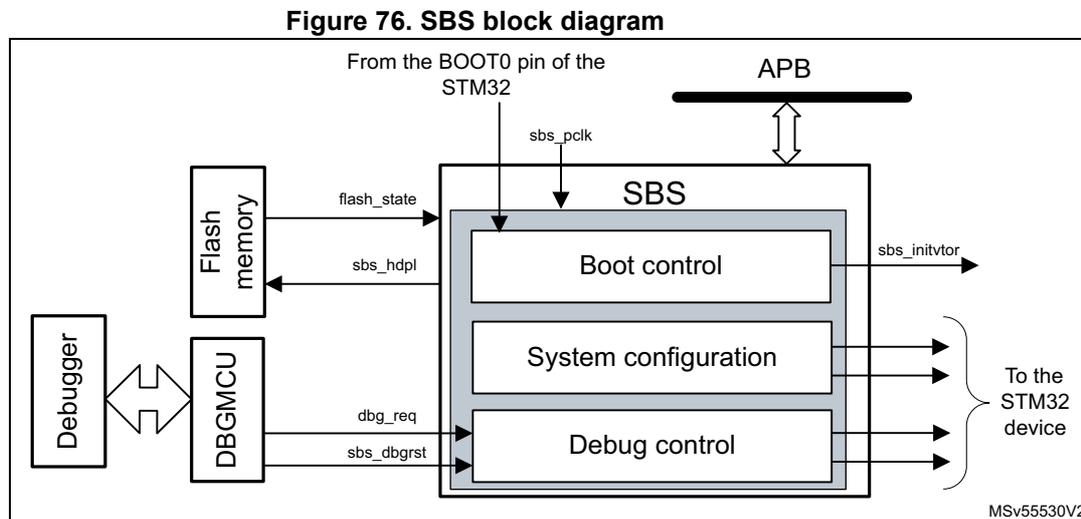
Figure 76. SBS block diagram
8.3.2 SBS internal signals
The tables below detail the SBS pins and internal signals.
Table 74. SBS input/output pins
| Pin name | Type | Description |
|---|---|---|
| BOOT | Input | Boot from flash memory or bootloader. |
Table 75. SBS internal input/output signals
| Signal name | Type | Description |
|---|---|---|
| sbs_pclk | Input | APB bus clock |
| sbs_dbgst | Debug configuration reset from DBGMCU | |
| flash_state | Non-volatile security status input from Flash memory | |
| sbs_hdpl | Output | Hide protection level information |
| sbs_initvtor | Vector address for Cortex-M7. See Section 8.3.5 for more details. | |
| dbg_req | Input | External host request to launch the debug authentication protocol. See Section 8.3.6 for more details. |
8.3.3 SBS reset and clocks
The SBS configuration port is clocked by the APB bus clock. There is a general reset and a debug configuration reset controlled in DBGMCU.
8.3.4 SBS hide protection management
The HDPL is a monotonic counter incremented during the boot stages. It is reset to its default value only following a power-on reset or a system reset. This default value (0 or 1) depends on the device lifecycle, as defined in Table 76: SBS boot control .
The device uses HDPL information to automatically isolate code and its associated secrets (like keys) during the boot process. Incrementing HDPL ensures that private code and data for one boot stage cannot be directly accessible from later boot stages.
Note: The use of HDPL in the embedded Flash memory is detailed in Section 5: Embedded flash memory (FLASH) .
The HDPL can take a 0 to 3 value. When reaching the value 3, HDPL keeps this value until reset. The current HDPL value is readable in HDPL bitfield in SBS_HDPLSR register.
Incrementing HDPL
The application must write 0x6A to INCR_HDPL bitfield in SBS_HDPLCR register to increment the HDPL by one.
After such increment, and before doing any subsequent action, the application must check if the HDPL has effectively been incremented, by reading SBS_HDPLSR.
8.3.5 SBS boot control
The figure below and Table 76 shows how the SBS uses multiple information to define the Cortex-M7 boot address (INITVTOR) and the HDPL before the CPU reset is released.
Figure 77. SBS boot control
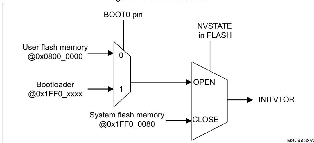
The diagram illustrates the SBS boot control logic. A 2-to-1 multiplexer (MUX) selects between two memory addresses based on the BOOT0 pin. The inputs are: 'User flash memory @0x0800_0000' (input 0) and 'Bootloader @0x1FF0_xxxx' (input 1). The output of this MUX is connected to the 'OPEN' input of a second 2-to-1 MUX. The second MUX also has a 'CLOSE' input connected to 'System flash memory @0x1FF0_0080'. The output of the second MUX is labeled 'INITVTOR'. The second MUX is controlled by the 'NVSTATE in FLASH' signal. The diagram is labeled with the reference 'MSV55532V2' in the bottom right corner.
Table 76. SBS boot control
| SBS input | SBS output | ||||
|---|---|---|---|---|---|
| NVSTATE (from FLASH) | BOOT pin | Boot address | INITVTOR
(1) (to Cortex-M7) | Immutable RoT selection (2) | HDPL value in SBS_HDPLSR |
| OPEN | 0 | User Flash memory | 0x0800 0000 | OEM | 1 |
| 1 | Bootloader (3) | ST | 2 | ||
| CLOSE | x | System Flash memory (ST RSS) | Defined by ST | Any | 0 |
1. Readable in SBS_BOOTSR register.
2. ST iRoT is not available on STM32H7Rx/7Sx devices.
3. Located in the system memory, it is used to reprogram the Flash memory by using USART, I2C, SPI, FDCAN or USB_OTG in device mode through the DFU (device firmware upgrade) (TBC)
The BOOT value coming from the external pin is latched upon reset release. This pin is in input mode during the complete reset phase, and then switches automatically in analog mode after reset is released.
The NVSTATE value comes from the Flash memory interface, following an automatic option-byte load sequence (see Section 5: Embedded flash memory (FLASH) for details).
8.3.6 SBS debug management
Device debug is allowed or not depending on the lifecycle of the device:
- • For open devices (NVSTATE = OPEN), the debug is always allowed.
- • For close devices (NVSTATE = CLOSE), the debug is disabled at boot but can be reopened during the boot after an authenticated debug sequence.
When debug is forbidden, mailbox access port, CM7 access port, and CPU debug interface are locked. In this situation, the debugger cannot access the CPU and no effective debug can be done. Refer to Section 66: Debug infrastructure for more details.
Authenticated debug sequence
- 1. External host requests to launch the debug authentication protocol, via the DBGMCU access port mailbox. The rest of the device is kept under reset.
- 2. SBS selects the ST RSS boot address and requests the CPU to be released from reset
- 3. CPU running RSS library executes the debug authentication library in system Flash memory. If the device is closed, the access port mailbox is closed until RSS acknowledges the authentication sequence start request.
- 4. As soon as a debug certificate is accepted by the device, RSS programs the opening of the Cortex-M7 access port by writing to AP_UNLOCK bitfield in SBS_DBGCR register. RSS also programs the opening of the CPU debug interface by writing to DBG_UNLOCK bitfield in SBS_DBGCR register.
- 5. Above re-openings are effective only when the HDPL in SBS_HDPLSR register has a value equal or superior to the value programmed in DBG_AUTH_HDPL in SBS_DBGCR register. If DBG_AUTH_HDPL bitfield is kept at 0x0, the debug never opens (forbidden value).
Note: The debug authentication library in system Flash memory is only available when HDPL = 0 in SBS_HDPLSR. Only this code can perform the above steps 3 and 4.
At any time, the application via DBGMCU can reset the debug configuration in SBS_DBGCR register. See dedicated sections for details (TBC).
Debug locking
To ensure the debug configuration is not modified by an unauthorized code, any application can lock it by writing to DBGCFG_LOCK bitfield in SBS_DBGLOCKR register. Once the debug configuration is locked, the application can unlock it using DBGMCU (TBC).
8.3.7 SBS voltage booster for I/O analog switches
By setting BOOSTEN in SBS_PMCR, the application reduces the total harmonic distortion (THD) of the I/O analog switches when the supply voltage is below 2.7 V, to guarantee the same performance as with the full voltage range.
To avoid current consumption due to booster activation when \( V_{DDA} < 2.7\text{ V} \) and \( V_{DD} > 2.7\text{ V} \) , \( V_{DD} \) can be selected as supply voltage for the analog switches, by setting BOOSTVDDSEL in SBS_PMCR.
In this case, BOOSTEN must be cleared to avoid unexpected power consumption.
Table 77. Analog switches recommended configuration
| \( V_{DDA} \) | \( V_{DD} \) | BOOSTEN | BOOSTVDDSEL | Analog switch supply voltage |
|---|---|---|---|---|
| \( \leq 2.7\text{ V} \) | \( \leq 2.7\text{ V} \) | 1 | 0 | Booster |
| \( > 2.7\text{ V} \) | 0 | 1 | \( V_{DD} \) | |
| \( > 2.7\text{ V} \) | 0 | 0 | \( V_{DDA} \) |
8.3.8 SBS I/O compensation cell management
The I/O compensation cell generates an 8-bit value for the I/O buffer (4 bits for N-MOS and 4 bits for P-MOS), that depends on PVT operating conditions (process, voltage, temperature). These bits are used to control the output impedance in the I/O buffer, and the slew rate of the I/O commutation (the \( t_{fall} \) and \( t_{rise} \) time), in order to reduce the I/O noise on power supply.
The CSI is used by the compensation cells and must be enabled before enabling the compensation cells
As shown in Figure 78 , the compensation cell is split into two blocks: one block to provide an optimal code for the current PVT, and one block to drive the block controlled by the software.
Figure 78. Compensation cell management
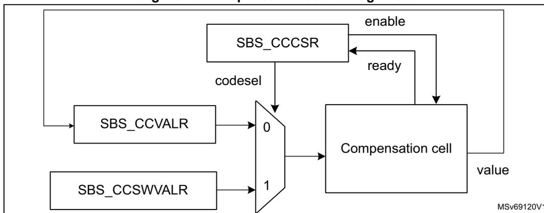
The compensation cell value can be read when the READY flag is set in SBS_CCCSR. With CODESEL in SBS_CCCSR, the application can select the value to apply between two options: the code from the cell or the code from SBS_CCSWVALR.
Three compensation cells are embedded in STM32H7Rx/7Sx devices:
- • one for the I/Os supplied by \( V_{DD} \) or \( V_{DDA} \) (see Section 8.3.7 )
- • one for the dedicated I/Os of the XSPI1
- • one for the dedicated I/Os of the XSPI2
By default, the compensation cells are disabled, and a fixed code is applied to all the I/Os.
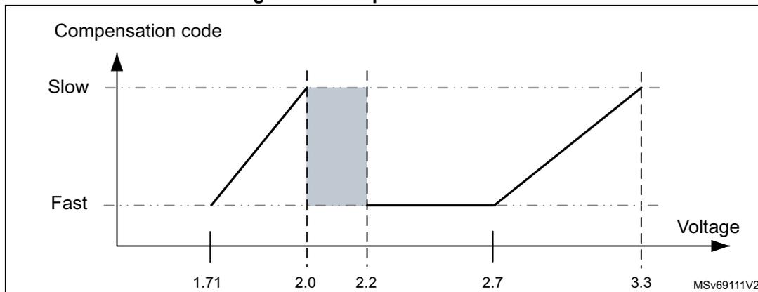
Note: The compensation cell can be used only when \( 2.7\text{ V} \leq V_{DDIOx} \leq 3.6\text{ V} \) or \( 1.71\text{ V} \leq V_{DDIOx} \leq 2\text{ V} \) (see the figure below).
Figure 79. Compensation cell use
8.3.9 SBS registers access control
Some SBS registers can be accessed only if HDPL = 0 in SBS_HDPLSR (hence only accessible by the ST RSS code).
Some bitfields in SBS are security critical, reset in non-secure state (coded as 0xB4) or in secure state (any other values). For bitfields reset in non-secure state, when the secure state is selected writing any value but 0xB4, the bitfield is no more writable until a reset occurs.
As a general rule, it is recommended to write 0xC3 to select a secure state and read back 0x6A to acknowledge the write is effective.
Protected fields are the following:
- • INCR_HDPL
- • DBGCFG_LOCK
8.3.10 SBS error management
The SBS does not manage errors.
8.4 SBS interrupts
The SBS does not support interrupts.
8.5 SBS registers
8.5.1 SBS boot status register (SBS_BOOTSR)
Address offset: 0x000
Reset value: 0x0000 0000
| 31 | 30 | 29 | 28 | 27 | 26 | 25 | 24 | 23 | 22 | 21 | 20 | 19 | 18 | 17 | 16 |
|---|---|---|---|---|---|---|---|---|---|---|---|---|---|---|---|
| INITVTOR[31:16] | |||||||||||||||
| r | r | r | r | r | r | r | r | r | r | r | r | r | r | r | r |
| 15 | 14 | 13 | 12 | 11 | 10 | 9 | 8 | 7 | 6 | 5 | 4 | 3 | 2 | 1 | 0 |
| INITVTOR[15:0] | |||||||||||||||
| r | r | r | r | r | r | r | r | r | r | r | r | r | r | r | r |
Bits 31:0 INITVTOR[31:0] : initial vector for Cortex-M7
This register includes the physical boot address used by the Cortex-M7 after reset
8.5.2 SBS hide protection control register (SBS_HDPLCR)
Address offset: 0x010
Reset value: 0x0000 00B4
| 31 | 30 | 29 | 28 | 27 | 26 | 25 | 24 | 23 | 22 | 21 | 20 | 19 | 18 | 17 | 16 |
|---|---|---|---|---|---|---|---|---|---|---|---|---|---|---|---|
| Res. | Res. | Res. | Res. | Res. | Res. | Res. | Res. | Res. | Res. | Res. | Res. | Res. | Res. | Res. | Res. |
| 15 | 14 | 13 | 12 | 11 | 10 | 9 | 8 | 7 | 6 | 5 | 4 | 3 | 2 | 1 | 0 |
| Res. | Res. | Res. | Res. | Res. | Res. | Res. | Res. | INCR_HDPL[7:0] | |||||||
| rW | rW | rW | rW | rW | rW | rW | rW | ||||||||
Bits 31:8 Reserved, must be kept at reset value.
Bits 7:0 INCR_HDPL[7:0] : increment HDPL
Write 0x6A to increment device HDPL by one.
After a write, the register value reverts to its default value (0xB4).
8.5.3 SBS hide protection status register (SBS_HDPLSR)
Address offset: 0x014
Reset value: 0x0000 00XX (see Section 8.3.5 )
| 31 | 30 | 29 | 28 | 27 | 26 | 25 | 24 | 23 | 22 | 21 | 20 | 19 | 18 | 17 | 16 |
|---|---|---|---|---|---|---|---|---|---|---|---|---|---|---|---|
| Res. | Res. | Res. | Res. | Res. | Res. | Res. | Res. | Res. | Res. | Res. | Res. | Res. | Res. | Res. | Res. |
| 15 | 14 | 13 | 12 | 11 | 10 | 9 | 8 | 7 | 6 | 5 | 4 | 3 | 2 | 1 | 0 |
| Res. | Res. | Res. | Res. | Res. | Res. | Res. | Res. | HDPL[7:0] | |||||||
| r | r | r | r | r | r | r | r | ||||||||
Bits 31:8 Reserved, must be kept at reset value.
Bits 7:0 HDPL[7:0] : hide protection level
This bitfield returns the current HDPL of the device.
0xB4: HDPL0, corresponding to ST-RSS (default when device is CLOSE)
0x51: HDPL1
0x8A: HDPL2
0x6F and other codes: HDPL3, corresponding to non-boot application.
Note: The device state (open/close) is defined in FLASH_NVSTATE register of the embedded Flash memory.
8.5.4 SBS debug control register (SBS_DBGCR)
Address offset: 0x020
Reset value: 0x0000 0000
| 31 | 30 | 29 | 28 | 27 | 26 | 25 | 24 | 23 | 22 | 21 | 20 | 19 | 18 | 17 | 16 |
|---|---|---|---|---|---|---|---|---|---|---|---|---|---|---|---|
| Res. | Res. | Res. | Res. | Res. | Res. | Res. | Res. | DBG_AUTH_HDPL[7:0] | |||||||
| rw | rw | rw | rw | rw | rw | rw | rw | ||||||||
| 15 | 14 | 13 | 12 | 11 | 10 | 9 | 8 | 7 | 6 | 5 | 4 | 3 | 2 | 1 | 0 |
| DBG_UNLOCK[7:0] | AP_UNLOCK[7:0] | ||||||||||||||
| rw | rw | rw | rw | rw | rw | rw | rw | rw | rw | rw | rw | rw | rw | rw | rw |
Bits 31:24 Reserved, must be kept at reset value.
Bits 23:16 DBG_AUTH_HDPL[7:0] : authenticated debug hide protection level
Writing to this bitfield defines at which HDPL the authenticated debug opens.
0x51: HDPL1
0x8A: HDPL2
0x6F: HDPL3
Note: Writing any other values is ignored. Reading any other value means the authenticated debug always fails.
Bits 15:8 DBG_UNLOCK[7:0] : debug unlock
Write 0xB4 to this bitfield to open the debug when HDPL in SBS_HDPLSR equals to DBG_AUTH_HDPL in this register.
Bits 7:0 AP_UNLOCK[7:0] : access port unlock
Write 0xB4 to this bitfield to open the device access port.
8.5.5 SBS debug lock register (SBS_DBGLOCKR)
Address offset: 0x024
Reset value: 0x0000 00B4
This register is reset when sbs_dbggrst is asserted.
| 31 | 30 | 29 | 28 | 27 | 26 | 25 | 24 | 23 | 22 | 21 | 20 | 19 | 18 | 17 | 16 |
|---|---|---|---|---|---|---|---|---|---|---|---|---|---|---|---|
| Res. | Res. | Res. | Res. | Res. | Res. | Res. | Res. | Res. | Res. | Res. | Res. | Res. | Res. | Res. | Res. |
| 15 | 14 | 13 | 12 | 11 | 10 | 9 | 8 | 7 | 6 | 5 | 4 | 3 | 2 | 1 | 0 |
| Res. | Res. | Res. | Res. | Res. | Res. | Res. | Res. | DBGCFG_LOCK[7:0] | |||||||
| rw | rw | rw | rw | rw | rw | rw | rw | ||||||||
Bits 31:8 Reserved, must be kept at reset value.
Bits 7:0 DBGCFG_LOCK[7:0] : debug configuration lock
Reading this bitfield returns 0x6A if the bitfield value is different from 0xB4.
0xB4: Writes to SBS_DBGCR allowed (default)
Other: Writes to SBS_DBGCR ignored
Note: 0xC3 is the recommended value to lock the debug configuration using this bitfield.
8.5.6 SBS RSS command register (SBS_RSSCMDR)
Address offset: 0x034
Reset value: 0x0000 0000
| 31 | 30 | 29 | 28 | 27 | 26 | 25 | 24 | 23 | 22 | 21 | 20 | 19 | 18 | 17 | 16 |
|---|---|---|---|---|---|---|---|---|---|---|---|---|---|---|---|
| Res. | Res. | Res. | Res. | Res. | Res. | Res. | Res. | Res. | Res. | Res. | Res. | Res. | Res. | Res. | Res. |
| 15 | 14 | 13 | 12 | 11 | 10 | 9 | 8 | 7 | 6 | 5 | 4 | 3 | 2 | 1 | 0 |
| RSSCMD[15:0] | |||||||||||||||
| rw | rw | rw | rw | rw | rw | rw | rw | rw | rw | rw | rw | rw | rw | rw | rw |
Bits 31:16 Reserved, must be kept at reset value.
Bits 15:0 RSSCMD[15:0] : RSS command
The application can use this bitfield to pass on a command to the RSS, executed at the next reset.
8.5.7 SBS product mode and configuration register (SBS_PMCR)
Address offset: 0x100
Reset value: 0x1000 0000
| 31 | 30 | 29 | 28 | 27 | 26 | 25 | 24 | 23 | 22 | 21 | 20 | 19 | 18 | 17 | 16 |
|---|---|---|---|---|---|---|---|---|---|---|---|---|---|---|---|
| Res. | Res. | Res. | AXISRAM_WS | Res. | Res. | Res. | Res. | ETH_PHYSEL[2:0] | Res. | Res. | Res. | Res. | Res. | ||
| rw | rw | rw | rw | ||||||||||||
| 15 | 14 | 13 | 12 | 11 | 10 | 9 | 8 | 7 | 6 | 5 | 4 | 3 | 2 | 1 | 0 |
| Res. | Res. | Res. | Res. | Res. | Res. | BOOSTVDDSEL | BOOSTEN | Res. | Res. | Res. | Res. | Res. | Res. | Res. | Res. |
| rw | rw | ||||||||||||||
Bits 31:29 Reserved, must be kept at reset value.
Bit 28 AXISRAM_WS : AXISRAM wait state
This bit is set to one by default to have one wait state on AXISRAM4 when ECC = 0. (Can be optionally set to 0)
0: No wait state added when accessing any AXISRAM4 with ECC = 0
1: One wait state added when accessing any AXISRAM4 with ECC = 0.
Bits 27:24 Reserved, must be kept at reset value.
Bits 23:21 ETH_PHYSEL[2:0] : Ethernet PHY interface selection
000: GMII or MII
100: RMII
Other: reserved
Bits 20:10 Reserved, must be kept at reset value.
Bit 9 BOOSTVDDSEL : booster \( V_{DD} \) selection
This bit selects the analog switch supply voltage, between \( V_{DD} \) , \( V_{DDA} \) and booster.
To avoid current consumption due to booster activation when \( V_{DDA} < 2.7\text{ V} \) and \( V_{DD} > 2.7\text{ V} \) , \( V_{DD} \) can be selected as supply voltage for analog switches. In this case, the BOOSTEN bit must be cleared to avoid unwanted power consumption.
When both \( V_{DD} \) and \( V_{DDA} \) are below \( 2.7\text{ V} \) , the booster is still needed to obtain full AC performances from the I/O analog switches.
0: \( V_{DDA} \) selected as analog switch booster voltage supply (when BOOSTEN bit is cleared)
1: \( V_{DD} \) selected as analog switch booster voltage supply
Bit 8 BOOSTEN : booster enable
Set this bit to reduce the THD of the analog switches when the supply voltage is below \( 2.7\text{ V} \) , guaranteeing the same performance as with the full voltage range. To avoid current consumption due to booster activation when \( V_{DDA} < 2.7\text{ V} \) and \( V_{DD} > 2.7\text{ V} \) , \( V_{DD} \) can be selected as supply voltage for analog switches by setting BOOSTVDDSEL bit in SBS_PMCR. In this case, the BOOSTEN bit must be cleared to avoid unwanted power consumption.
0: Booster disabled
1: Booster enabled
Bits 7:0 Reserved, must be kept at reset value.
8.5.8 SBS FPU interrupt mask register (SBS_FPUIMR)
Address offset: 0x104
Reset value: 0x0000 001F
| 31 | 30 | 29 | 28 | 27 | 26 | 25 | 24 | 23 | 22 | 21 | 20 | 19 | 18 | 17 | 16 |
|---|---|---|---|---|---|---|---|---|---|---|---|---|---|---|---|
| Res. | Res. | Res. | Res. | Res. | Res. | Res. | Res. | Res. | Res. | Res. | Res. | Res. | Res. | Res. | Res. |
| 15 | 14 | 13 | 12 | 11 | 10 | 9 | 8 | 7 | 6 | 5 | 4 | 3 | 2 | 1 | 0 |
| Res. | Res. | Res. | Res. | Res. | Res. | Res. | Res. | Res. | Res. | FPU_IE[5:0] | |||||
| rw | rw | rw | rw | rw | rw | ||||||||||
Bits 31:6 Reserved, must be kept at reset value.
Bits 5:0 FPU_IE[5:0] : FPU interrupt enable
Set and cleared by software to enable the Cortex-M7 FPU interrupts
xxxxx1: Invalid operation interrupt enabled (xxxxx0 to disable)
xxxx1x: Divide-by-zero interrupt enabled (xxxx0x to disable)
xxx1xx: Underflow interrupt enabled (xxx0xx to disable)
xx1xxx: Overflow interrupt enabled (xx0xxx to disable)
x1xxxx: Input denormal interrupt enabled (x0xxxx to disable)
1xxxxx: Inexact interrupt enabled (0xxxxx to disable), disabled by default
8.5.9 SBS memory erase status register (SBS_MESR)
Address offset: 0x108
Reset value: 0x0000 0000
| 31 | 30 | 29 | 28 | 27 | 26 | 25 | 24 | 23 | 22 | 21 | 20 | 19 | 18 | 17 | 16 |
|---|---|---|---|---|---|---|---|---|---|---|---|---|---|---|---|
| Res. | Res. | Res. | Res. | Res. | Res. | Res. | Res. | Res. | Res. | Res. | Res. | Res. | Res. | Res. | Res. |
| 15 | 14 | 13 | 12 | 11 | 10 | 9 | 8 | 7 | 6 | 5 | 4 | 3 | 2 | 1 | 0 |
| Res. | Res. | Res. | Res. | Res. | Res. | Res. | Res. | Res. | Res. | Res. | Res. | Res. | Res. | Res. | MEF |
| r |
Bits 31:1 Reserved, must be kept at reset value.
Bit 0 MEF : memory erase flag
This bit is set by hardware when BKPRAM and PKA SRAM erase is ongoing after a power-on reset or one tamper event (see Section 50: Tamper and backup registers (TAMP) for details). This bit is set when the erase is done.
0: Automatic erase of BKPRAM and PKA RAM memories ongoing
1: Automatic erase of BKPRAM and PKA RAM memories done
8.5.10 SBS I/O compensation cell control and status register (SBS_CCCSR)
Address offset: 0x110
Reset value: 0x0000 0000
For more details on this register, refer to Section 8.3.7 and Section 8.3.8 .
| 31 | 30 | 29 | 28 | 27 | 26 | 25 | 24 | 23 | 22 | 21 | 20 | 19 | 18 | 17 | 16 |
|---|---|---|---|---|---|---|---|---|---|---|---|---|---|---|---|
| Res. | Res. | Res. | Res. | Res. | Res. | Res. | Res. | Res. | Res. | Res. | Res. | Res. | XSPI2_IOHSLV | XSPI1_IOHSLV | IOHSLV |
| rw | rw | rw | |||||||||||||
| 15 | 14 | 13 | 12 | 11 | 10 | 9 | 8 | 7 | 6 | 5 | 4 | 3 | 2 | 1 | 0 |
| Res. | Res. | Res. | Res. | Res. | XSPI2_COMP_RDY | XSPI1_COMP_RDY | COMP_RDY | Res. | Res. | XSPI2_COMP_CODESEL | XSPI2_COMP_EN | XSPI1_COMP_CODESEL | XSPI1_COMP_EN | COMP_CODESEL | COMP_EN |
| rw | rw | rw | rw | rw | rw | rw | rw | rw |
Bits 31:19 Reserved, must be kept at reset value.
Bit 18 XSPI2_IOHSLV: XSPIM_P2 I/O high speed at low voltageWhen this bit is set, the speed of the XSPIM_P2 I/Os is optimized when the device voltage is low.
This bit is active only if XSPI2_HSLV user option bit is set in FLASH. This bit must be used only if the device supply voltage is below 2.7 V. Setting this bit when \( V_{DD} \) is higher than 2.7 V may be destructive.
0: No XSPIM_P2 I/O speed optimization when device voltage is low
1: XSPIM_P2 I/O speed optimized when device voltage is low, if XSPI2_HSLV user option is set (no effect otherwise)
Bit 17 XSPI1_IOHSLV: XSPIM_P1 I/O high speed at low voltageWhen this bit is set, the speed of the XSPIM_P1 I/Os is optimized when the device voltage is low.
This bit is active only if XSPI1_HSLV user option bit is set in FLASH. This bit must be used only if the device supply voltage is below 2.7 V. Setting this bit when \( V_{DD} \) is higher than 2.7 V may be destructive.
0: No XSPIM_P1 I/O speed optimization when device voltage is low
1: XSPIM_P1 I/O speed optimized when device voltage is low, if XSPI1_HSLV user option is set (no effect otherwise)
Bit 16 IOHSLV: I/O high speed at low voltageWhen this bit is set, the speed of the I/Os is optimized when the device voltage is low.
This bit is active only if VDDIO_HSLV user option bit is set in FLASH. It must be used only if the device supply voltage is below 2.7 V. Setting this bit when \( V_{DD} \) is higher than 2.7 V may be destructive.
0: No I/O speed optimization when device voltage is low
1: I/O speed optimized when device voltage is low, if VDDIO_HSLV user option is set (no effect otherwise)
Bits 15:11 Reserved, must be kept at reset value.
Bit 10 XSPI2_COMP_RDY: XSPIM_P2 compensation cell readyThis bit provides the status of the XSPIM_P2 compensation cell.
0: XSPIM_P2 I/O compensation cell not ready
1: XSPIM_P2 I/O compensation cell ready. The code value provided by the cell can be used
Note: The CSI clock is required for the compensation cell to work properly. The compensation cell ready bit (XSPI2_COMP_RDY) is not set if the CSI clock is not enabled.
Bit 9 XSPI1_COMP_RDY: XSPIM_P1 compensation cell readyThis bit provides the status of the XSPIM_P1 compensation cell.
0: XSPIM_P1 I/O compensation cell not ready
1: XSPIM_P1 I/O compensation cell ready. The code value provided by the cell can be used
Note: The CSI clock is required for the compensation cell to work properly. The compensation cell ready bit (XSPI1_COMP_RDY) is not set if the CSI clock is not enabled.
Bit 8 COMP_RDY: Compensation cell readyThis bit provides the status of the compensation cell.
0: I/O compensation cell not ready
1: I/O compensation cell ready. The code value provided by the cell can be used.
Note: The CSI clock is required for the compensation cell to work properly. The compensation cell ready bit (COMP_RDY) is not set if the CSI clock is not enabled.
Bits 7:6 Reserved, must be kept at reset value.
Bit 5 XSPI2_COMP_CODESEL : XSPIM_P2 compensation cell code selection
This bit selects the code to be applied for the XSPIM_P2 I/O compensation cell.
0: Code from the cell (available in the SBS_CCVALR)
1: Code from the SBS software value register (SBS_CCSWVALR)
Bit 4 XSPI2_COMP_EN : XSPIM_P2 compensation cell enable
Set this bit to enable the XSPIM_P2 compensation cell.
0: XSPIM_P2 compensation cell disabled
1: XSPIM_P2 compensation cell enabled
Bit 3 XSPI1_COMP_CODESEL : XSPIM_P1 compensation cell code selection
This bit selects the code to be applied for the XSPIM_P1 I/O compensation cell.
0: Code from the cell (available in the SBS_CCVALR)
1: Code from the SBS software value register (SBS_CCSWVALR)
Bit 2 XSPI1_COMP_EN : XSPIM_P1 compensation cell enable
Set this bit to enable the XSPIM_P1 compensation cell.
0: XSPIM_P1 compensation cell disabled
1: XSPIM_P1 compensation cell enabled
Bit 1 COMP_CODESEL : Compensation cell code selection
This bit selects the code to be applied for the I/O compensation cell.
0: Code from the cell (available in the SBS_CCVALR)
1: Code from the SBS software value register (SBS_CCSWVALR)
Bit 0 COMP_EN : Compensation cell enable
Set this bit to enable the compensation cell.
0: Compensation cell disabled
1: Compensation cell enabled
8.5.11 SBS compensation cell for I/Os value register (SBS_CCVALR)
Address offset: 0x114
Reset value: 0x0000 0088
Reset: system reset
For more details on this register, refer to Section 8.3.8 .
| 31 | 30 | 29 | 28 | 27 | 26 | 25 | 24 | 23 | 22 | 21 | 20 | 19 | 18 | 17 | 16 |
|---|---|---|---|---|---|---|---|---|---|---|---|---|---|---|---|
| Res. | Res. | Res. | Res. | Res. | Res. | Res. | Res. | XSPI2_PSRC[3:0] | XSPI2_NSRC[3:0] | ||||||
| r | r | r | r | r | r | r | r | ||||||||
| 15 | 14 | 13 | 12 | 11 | 10 | 9 | 8 | 7 | 6 | 5 | 4 | 3 | 2 | 1 | 0 |
| XSPI1_PSRC[3:0] | XSPI1_NSRC[3:0] | PSRC[3:0] | NSRC[3:0] | ||||||||||||
| r | r | r | r | r | r | r | r | r | r | r | r | r | r | r | r |
Bits 31:24 Reserved, must be kept at reset value.
Bits 23:20 XSPI2_PSRC[3:0] : XSPIM_P2 PMOS transistors slew-rate compensation
This bitfield returns the PMOS transistors slew-rate compensation value computed by the cell. It is interpreted by XSPIM_P2 to compensate the PMOS transistors slew rate in the functional range if XSPI2_COMP_CODESEL = 0 in SBS_CCCSR register.
Bits 19:16 XSPI2_NSRC[3:0] : XSPIM_P2 NMOS transistors slew-rate compensation
This bitfield returns the NMOS transistors slew-rate compensation value computed by the cell. It is interpreted by XSPIM_P2 to compensate the NMOS transistors slew rate in the functional range if XSPI2_COMP_CODESEL = 0 in SBS_CCCSR register.
Bits 15:12 XSPI1_PSRC[3:0] : XSPIM_P1 PMOS transistors slew-rate compensation
This bitfield returns the PMOS transistors slew-rate compensation value computed by the cell. It is interpreted by XSPIM_P1 to compensate the PMOS transistors slew rate in the functional range if XSPI1_COMP_CODESEL = 0 in SBS_CCCSR register.
Bits 11:8 XSPI1_NSRC[3:0] : XSPIM_P1 NMOS transistors slew-rate compensation
This bitfield returns the NMOS transistors slew-rate compensation value computed by the cell. It is interpreted by XSPIM_P1 to compensate the NMOS transistors slew rate in the functional range if XSPI1_COMP_CODESEL = 0 in SBS_CCCSR register.
Bits 7:4 PSRC[3:0] : PMOS transistors slew-rate compensation
This bitfield returns the PMOS transistors slew-rate compensation value computed by the cell. It is interpreted to compensate the PMOS transistors slew rate in the functional range if COMP_CODESEL = 0 in SBS_CCCSR register.
Bits 3:0 NSRC[3:0] : NMOS transistors slew-rate compensation
This bitfield returns the NMOS transistors slew-rate compensation value computed by the cell. It is interpreted to compensate the NMOS transistors slew rate in the functional range if COMP_CODESEL = 0 in SBS_CCCSR register.
8.5.12 SBS compensation cell for I/Os software value register (SBS_CCSWVALR)
Address offset: 0x118
Reset value: 0x0000 0088
For more details on this register, refer to Section 8.3.8 .
| 31 | 30 | 29 | 28 | 27 | 26 | 25 | 24 | 23 | 22 | 21 | 20 | 19 | 18 | 17 | 16 |
|---|---|---|---|---|---|---|---|---|---|---|---|---|---|---|---|
| Res. | Res. | Res. | Res. | Res. | Res. | Res. | Res. | XSPI2_SW_PSRC[3:0] | XSPI2_SW_NSRC[3:0] | ||||||
| rw | rw | rw | rw | rw | rw | rw | rw | ||||||||
| 15 | 14 | 13 | 12 | 11 | 10 | 9 | 8 | 7 | 6 | 5 | 4 | 3 | 2 | 1 | 0 |
| XSPI1_SW_PSRC[3:0] | XSPI1_SW_NSRC[3:0] | SW_PSRC[3:0] | SW_NSRC[3:0] | ||||||||||||
| rw | rw | rw | rw | rw | rw | rw | rw | rw | rw | rw | rw | rw | rw | rw | rw |
Bits 31:24 Reserved, must be kept at reset value.
Bits 23:20 XSPI2_SW_PSRC[3:0] : XSPIM_P2 software PMOS transistors slew-rate compensation
This bitfield returns the PMOS transistors slew-rate compensation value computed by the cell. It is interpreted by XSPIM_P2 to compensate the PMOS transistors slew rate in the functional range if XSPI2_COMP_CODESEL = 1 in SBS_CCCSR register.
Bits 19:16 XSPI2_SW_NSRC[3:0] : XSPIM_P2 software NMOS transistors slew-rate compensation
This bitfield returns the NMOS transistors slew-rate compensation value computed by the cell. It is interpreted by XSPIM_P2 to compensate the NMOS transistors slew rate in the functional range if XSPI2_COMP_CODESEL = 1 in SBS_CCCSR register.
Bits 15:12 XSPI1_SW_PSRC[3:0] : XSPIM_P1 software PMOS transistors slew-rate compensation
This bitfield returns the PMOS transistors slew-rate compensation value computed by the cell. It is interpreted by XSPIM_P1 to compensate the PMOS transistors slew rate in the functional range if XSPI1_COMP_CODESEL = 1 in SBS_CCCSR register.
Bits 11:8 XSPI1_SW_NSRC[3:0] : XSPIM_P1 software NMOS transistors slew-rate compensation
This bitfield returns the NMOS transistors slew -ate compensation value computed by the cell. It is interpreted by XSPIM_P1 to compensate the NMOS transistors slew rate in the functional range if XSPI1_COMP_CODESEL = 1 in SBS_CCCSR register.
Bits 7:4 SW_PSRC[3:0] : Software PMOS transistors slew-rate compensation
This bitfield returns the PMOS transistors slew-rate compensation value computed by the cell. It is interpreted to compensate the PMOS transistors slew rate in the functional range if COMP_CODESEL = 1 in SBS_CCCSR register.
Bits 3:0 SW_NSRC[3:0] : Software NMOS transistors slew-rate compensation
This bitfield returns the NMOS transistors slew-rate compensation value computed by the cell. It is interpreted to compensate the NMOS transistors slew rate in the functional range if COMP_CODESEL = 1 in SBS_CCCSR register.
8.5.13 SBS break lockup register (SBS_BKLOCKR)
Address offset: 0x120
Reset value: 0x0000 0088
| 31 | 30 | 29 | 28 | 27 | 26 | 25 | 24 | 23 | 22 | 21 | 20 | 19 | 18 | 17 | 16 |
|---|---|---|---|---|---|---|---|---|---|---|---|---|---|---|---|
| Res. | Res. | Res. | Res. | Res. | Res. | Res. | Res. | ARAM1ECC_BL | Res. | ARAM3ECC_BL | Res. | Res. | Res. | Res. | Res. |
| 15 | 14 | 13 | 12 | 11 | 10 | 9 | 8 | 7 | 6 | 5 | 4 | 3 | 2 | 1 | 0 |
| Res. | ITCMECC_BL | DTCMECC_BL | Res. | Res. | Res. | Res. | Res. | BKRAMECC_BL | CM7LOCKUP_BL | Res. | Res. | FLASHICC_BL | PVD_BL | Res. | Res. |
| rs | rs | rs | rs | rs | rs |
Bits 31:24 Reserved, must be kept at reset value.
Bit 23 ARAM1ECC_BL : AXISRAM1 ECC error break lock
Set this bit to enable and lock the connection between AXISRAM1 ECC double error detection flag and break inputs of TIM1/15/16/17 peripherals.
Once set, this bit is cleared only by a system reset.
0: AXISRAM1 ECC double error detection flag disconnected from TIM1/5/16/17 break inputs
1: AXISRAM1 ECC double error detection flag connected to TIM1/15/16/17 break inputs
Bit 22 Reserved, must be kept at reset value.
Bit 21 ARAM3ECC_BL : AXISRAM3 ECC error break lock
Set this bit to enable and lock the connection between AXISRAM3 ECC double error detection flag and break inputs of TIM1/15/16/17 peripherals.
Once set this bit is cleared only by a system reset.
0: AXISRAM3 ECC double error detection flag disconnected from TIM1/15/16/17 break inputs
1: AXISRAM3 ECC double error detection flag connected to TIM1/15/16/17 break inputs
Bits 20:15 Reserved, must be kept at reset value.
Bit 14 ITCMECC_BL : ITCM ECC error break lock
Set this bit to enable and lock the connection between ITCM ECC double error detection flag and break inputs of TIM1/15/16/17 peripherals.
Once set, this bit is cleared only by a system reset.
0: ITCM ECC double error detection flag disconnected from TIM1/15/16/17 break inputs
1: ITCM ECC double error detection flag connected to TIM1/15/16/17 break inputs
Bit 13 DTCMECC_BL : DTCM ECC error break lock
Set this bit to enable and lock the connection between DTCM ECC double error detection flag and break inputs of TIM1/15/16/17 peripherals.
Once set, this bit is cleared only by a system reset.
0: DTCM ECC double error detection flag disconnected from TIM1/15/16/17 break inputs
1: DTCM ECC double error detection flag connected to TIM1/15/16/17 break inputs
Note: The DTCM0 and DTCM1 are Or'ed to give DTCMECC
Bits 12:8 Reserved, must be kept at reset value.
Bit 7 BKRAMECC_BL : Backup RAM ECC error break lock
Set this bit to enable and lock the connection between backup RAM ECC double error detection flag and break inputs of TIM1/15/16/17 peripherals.
Once set, this bit is cleared only by a system reset.
0: Backup RAM ECC double error detection flag disconnected from TIM1/15/16/17 break inputs.
1: Backup RAM ECC double error detection flag connected to TIM1/15/16/17 break inputs.
Bit 6 CM7LCKUP_BL : Cortex-M7 lockup break lock
Set this bit to enable and lock the connection between the Cortex-M7 lockup (HardFault) output and break inputs of TIM1/15/16/17 peripherals.
Once set, this bit is cleared only by a system reset.
0: Cortex-M7 lockup output disconnected from TIM1/15/16/17 break inputs
1: Cortex-M7 lockup output connected to TIM1/15/16/17 break inputs
Bits 5:4 Reserved, must be kept at reset value.
Bit 3 FLASHECC_BL : Flash ECC error break lock
Set this bit to enable and lock the connection between embedded flash memory ECC double error detection flag and break inputs of TIM1/15/16/17 peripherals.
Once set, this bit is cleared only by a system reset.
0: FLASH ECC double error detection flag disconnected from TIM1/15/16/17 break inputs
1: FLASH ECC double error detection flag connected to TIM1/15/16/17 break inputs
Bit 2 PVD_BL : PVD break lock
This bit is set by SW and cleared only by a system reset. it can be used to enable and lock the connection to TIM1/8/15/16/17Break input as well as the PVDE and PLS[2:0] bitfields in the PWR_CR1 register.
Once set, this bit is cleared only by a system reset.
0: PVD interrupt disconnected from TIM1/8/15/16/17 break inputs. PVDE and PLS[2:0] bitfields can be programmed by the application.
1: PVD output connected to TIM1/8/15/16/17 break input. PVDE and PLS[2:0] bits are read only.
Bits 1:0 Reserved, must be kept at reset value.
8.5.14 SBS external interrupt configuration register x (SBS_EXTICRx)
Address offset: 0x130 + 0x4 * (x-1) (x = 1 to 4)
Reset value: 0x0000 0000
| 31 | 30 | 29 | 28 | 27 | 26 | 25 | 24 | 23 | 22 | 21 | 20 | 19 | 18 | 17 | 16 |
|---|---|---|---|---|---|---|---|---|---|---|---|---|---|---|---|
| Res. | Res. | Res. | Res. | Res. | Res. | Res. | Res. | Res. | Res. | Res. | Res. | Res. | Res. | Res. | Res. |
| 15 | 14 | 13 | 12 | 11 | 10 | 9 | 8 | 7 | 6 | 5 | 4 | 3 | 2 | 1 | 0 |
| PC_EXTI{(x-1) * 4 + 3} | PC_EXTI{(x-1) * 4 + 2} | PC_EXTI{(x-1) * 4 + 1} | PC_EXTI{(x-1) * 4} | ||||||||||||
| r | r | r | r | r | r | r | r | r | r | r | r | r | r | r | r |
Bits 31:16 Reserved, must be kept at reset value.
Bits 15:0
PC_EXTI{(x-1) * 4 + i} : Port configuration EXTI {x * 4 + i} (i = 0 to 3)
This bitfield selects the source input to the EXTI input {(x-1) * 4 + i} used for external interrupt/event detection.
0x0: PA[(x-1)*4+i] pin
0x1: PB[(x-1)*4+i] pin
0x2: PC[(x-1)*4+i] pin
0x3: PD[(x-1)*4+i] pin
0x4: PE[(x-1)*4+i] pin
0x5: PF[(x-1)*4+i] pin
0x6: PG[(x-1)*4+i] pin
0x7: PH[(x-1)*4+i] pin
0xC: PM[(x-1)*4+i] pin
0xD: PN[(x-1)*4+i] pin
0xE: PO[(x-1)*4+i] pin
0xF: PP[(x-1)*4+i] pin
Others: reserved
8.5.15 SBS register map
Table 78. SBS register map and reset values
| Offset | Register name | 31 | 30 | 29 | 28 | 27 | 26 | 25 | 24 | 23 | 22 | 21 | 20 | 19 | 18 | 17 | 16 | 15 | 14 | 13 | 12 | 11 | 10 | 9 | 8 | 7 | 6 | 5 | 4 | 3 | 2 | 1 | 0 | ||
|---|---|---|---|---|---|---|---|---|---|---|---|---|---|---|---|---|---|---|---|---|---|---|---|---|---|---|---|---|---|---|---|---|---|---|---|
| 0x000 | SBS_BOOTSR | INITVOR[31:0] | |||||||||||||||||||||||||||||||||
| Reset value | 0 | 0 | 0 | 0 | 0 | 0 | 0 | 0 | 0 | 0 | 0 | 0 | 0 | 0 | 0 | 0 | 0 | 0 | 0 | 0 | 0 | 0 | 0 | 0 | 0 | 0 | 0 | 0 | 0 | 0 | 0 | 0 | |||
| 0x010 | SBS_HDPLCR | Res. | Res. | Res. | Res. | Res. | Res. | Res. | Res. | Res. | Res. | Res. | Res. | Res. | Res. | Res. | Res. | Res. | Res. | Res. | Res. | Res. | Res. | Res. | Res. | INCR_HDPL[7:0] | |||||||||
| Reset value | 1 | 0 | 1 | 1 | 0 | 1 | 0 | 0 | |||||||||||||||||||||||||||
| 0x014 | SBS_HDPLSR | Res. | Res. | Res. | Res. | Res. | Res. | Res. | Res. | Res. | Res. | Res. | Res. | Res. | Res. | Res. | Res. | Res. | Res. | Res. | Res. | Res. | Res. | Res. | Res. | HDPL[7:0] | |||||||||
| Reset value | X | X | X | X | X | X | X | X | |||||||||||||||||||||||||||
| 0x018 | Reserved | Reserved | |||||||||||||||||||||||||||||||||
| 0x020 | SBS_DBGCR | Res. | Res. | Res. | Res. | Res. | Res. | Res. | Res. | DBG_AUTH_HDPL[7:0] | DBG_UNLOCK[7:0] | AP_UNLOCK[7:0] | |||||||||||||||||||||||
| Reset value | 0 | 0 | 0 | 0 | 0 | 0 | 0 | 0 | 0 | 0 | 0 | 0 | 0 | 0 | 0 | 0 | 0 | 0 | 0 | 0 | 0 | 0 | 0 | 0 | |||||||||||
| 0x024 | SBS_DBGLOCKR | Res. | Res. | Res. | Res. | Res. | Res. | Res. | Res. | Res. | Res. | Res. | Res. | Res. | Res. | Res. | Res. | Res. | Res. | Res. | Res. | Res. | Res. | Res. | Res. | DBGCFG_LOCK[7:0] | |||||||||
| Reset value | 1 | 0 | 1 | 1 | 0 | 1 | 0 | 0 | |||||||||||||||||||||||||||
| 0x028 to 0x030 | Reserved | Reserved | |||||||||||||||||||||||||||||||||
| 0x034 | SBS_RSSCMDR | Res. | Res. | Res. | Res. | Res. | Res. | Res. | Res. | Res. | Res. | Res. | Res. | Res. | Res. | Res. | Res. | RSSCMD[15:0] | |||||||||||||||||
| Reset value | 0 | 0 | 0 | 0 | 0 | 0 | 0 | 0 | 0 | 0 | 0 | 0 | 0 | 0 | 0 | 0 | |||||||||||||||||||
| 0x038 to 0x0FC | Reserved | Reserved | |||||||||||||||||||||||||||||||||
| 0x100 | SBS_PMCR | Res. | Res. | Res. | AXIARAM_WS | Res. | Res. | Res. | Res. | Res. | ETH_SEL_PHY [2:0] | Res. | Res. | Res. | Res. | Res. | Res. | Res. | Res. | Res. | Res. | Res. | Res. | BOOSTVDDSEL | BOOSTEN | Res. | Res. | Res. | Res. | Res. | Res. | Res. | Res. | ||
| Reset value | 0 | 0 | 0 | 0 | 0 | 0 | |||||||||||||||||||||||||||||
| 0x104 | SBS_FPUIMR | Res. | Res. | Res. | Res. | Res. | Res. | Res. | Res. | Res. | Res. | Res. | Res. | Res. | Res. | Res. | Res. | Res. | Res. | Res. | Res. | Res. | Res. | Res. | Res. | Res. | Res. | FPU_IE[5:0] | |||||||
| Reset value | 1 | 1 | 1 | 1 | 1 | 1 | |||||||||||||||||||||||||||||
| 0x108 | SBS_MESR | Res. | Res. | Res. | Res. | Res. | Res. | Res. | Res. | Res. | Res. | Res. | Res. | Res. | Res. | Res. | Res. | Res. | Res. | Res. | Res. | Res. | Res. | Res. | Res. | Res. | Res. | Res. | Res. | Res. | Res. | Res. | MEF | ||
| Reset value | 0 | ||||||||||||||||||||||||||||||||||
| 0x110 | SBS_CCCSR | Res. | Res. | Res. | Res. | Res. | Res. | Res. | Res. | Res. | Res. | Res. | Res. | Res. | Res. | Res. | XSPI2_IOHSLV | XSPI1_IOHSLV | IOHSLV | Res. | Res. | Res. | Res. | Res. | Res. | XSPI2_COMP_RDY | XSPI1_COMP_RDY | COMP_RDY | Res. | XSPI2_COMP_CODESEL | XSPI2_COMP_EN | XSPI1_COMP_CODESEL | XSPI1_COMP_EN | COMP_CODESEL | COMP_EN |
| Reset value | 0 | 0 | 0 | 0 | 0 | 0 | 0 | 0 | 0 | 0 | 0 | 0 | |||||||||||||||||||||||
| 0x114 | SBS_CCVALR | Res. | Res. | Res. | Res. | Res. | Res. | Res. | Res. | XSPI2_PSRC [3:0] | XSPI2_NSRC [3:0] | XSPI1_PSRC [3:0] | XSPI1_NSRC [3:0] | PSRC[3:0] | NSRC[3:0] | ||||||||||||||||||||
| Reset value | 0 | 0 | 0 | 0 | 0 | 0 | 0 | 0 | 0 | 0 | 0 | 0 | 0 | 0 | 0 | 0 | 1 | 0 | 0 | 0 | 1 | 0 | 0 | 0 | |||||||||||
| 0x118 | SBS_CCSWVALR | Res. | Res. | Res. | Res. | Res. | Res. | Res. | Res. | XSPI2_SW_PSRC [3:0] | XSPI2_SW_NSRC [3:0] | XSPI1_SW_PSRC [3:0] | XSPI1_SW_NSRC [3:0] | SW_PSRC [3:0] | SW_NSRC [3:0] | ||||||||||||||||||||
| Reset value | 0 | 0 | 0 | 0 | 0 | 0 | 0 | 0 | 0 | 0 | 0 | 0 | 0 | 0 | 0 | 0 | 1 | 0 | 0 | 0 | 1 | 0 | 0 | 0 | |||||||||||
Table 78. SBS register map and reset values (continued)
| Offset | Register name | 31 | 30 | 29 | 28 | 27 | 26 | 25 | 24 | 23 | 22 | 21 | 20 | 19 | 18 | 17 | 16 | 15 | 14 | 13 | 12 | 11 | 10 | 9 | 8 | 7 | 6 | 5 | 4 | 3 | 2 | 1 | 0 | |
|---|---|---|---|---|---|---|---|---|---|---|---|---|---|---|---|---|---|---|---|---|---|---|---|---|---|---|---|---|---|---|---|---|---|---|
| 0x120 | SBS_BKLOCKR | Res. | Res. | Res. | Res. | Res. | Res. | Res. | Res. | ARAM1ECC_BL | ARAM2ECC_BL | ARAM3ECC_BL | ARAM4ECC_BL | Res. | Res. | Res. | Res. | Res. | Res. | ITOMECC_BL | DTOMECC_BL | HRAM1ECC_BL | HRAM2ECC_BL | Res. | Res. | Res. | BKRAMECC_BL | CM7LCKUP_BL | Res. | Res. | FLASH ECC_BL | PVD_BL | Res. | Res. |
| Reset value | 0 | 0 | 0 | 0 | 0 | 0 | 0 | 0 | 1 | 0 | 1 | 0 | ||||||||||||||||||||||
| 0x024 to 0x02C | Reserved | Reserved | ||||||||||||||||||||||||||||||||
| 0x130 + 0x004 * x- 1 (x=1 to 4) | SBS_EXTICRx | Res. | Res. | Res. | Res. | Res. | Res. | Res. | Res. | Res. | Res. | Res. | Res. | Res. | Res. | Res. | Res. | Res. | Res. | PC_EXTI {x * 4 + 3} | PC_EXTI {x * 4 + 2} | PC_EXTI {x * 4 + 1} | PC_EXTI {x * 4} | |||||||||||
| Reset value | 0 | 0 | 0 | 0 | 0 | 0 | 0 | 0 | 0 | 0 | 0 | 0 | 0 | 0 | ||||||||||||||||||||