7. Reset and clock control (RCC)
The RCC block manages the clock and reset generation for the whole microcontroller.
The operating modes to which this section refers are defined in Section 6.6.1: Operating modes of the PWR block.
7.1 RCC main features
AHB-Lite bus interface
Reset block:
- – Generation of local and system reset
- – Bidirectional pin reset allowing to reset the microcontroller or external devices
- – WWDG and IWDG reset supported
- – Power-on (POR) and Brownout (BOR) resets initiated by the power control (PWR)
Clock generation block:
- • Generation and dispatching of clocks for the complete device
- • 3 separate PLLs using integer or fractional ratios
- • Possibility of changing the PLL fractional ratios on-the-fly
- • Smart clock gating to reduce power dissipation
- • System clock protection
- • 2 external oscillators:
- – High-speed external oscillator (HSE) supporting a wide range of crystals from 4 to 50 MHz frequency (a)
- – Low-speed external oscillator (LSE) for the 32 kHz crystals
- • 4 internal oscillators
- – High-speed internal oscillator (HSI)
- – 48 MHz RC oscillator (HSI48)
- – Low-power internal oscillator (CSI)
- – Low-speed internal oscillator (LSI)
- • Buffered clock outputs for external devices
- • Generation of two types of interrupts lines:
- – Dedicated interrupt lines for clock security management
- – One general interrupt line for other events
- • Clock generation handling in Stop and Standby mode
a. Note that when the USBHSPHY is used, the HSE frequency must be 16, 19.2, 20, 24, 26 or 32 MHz.
7.2 RCC block diagram
Figure 37 shows the RCC block diagram.
Figure 37. RCC block diagram
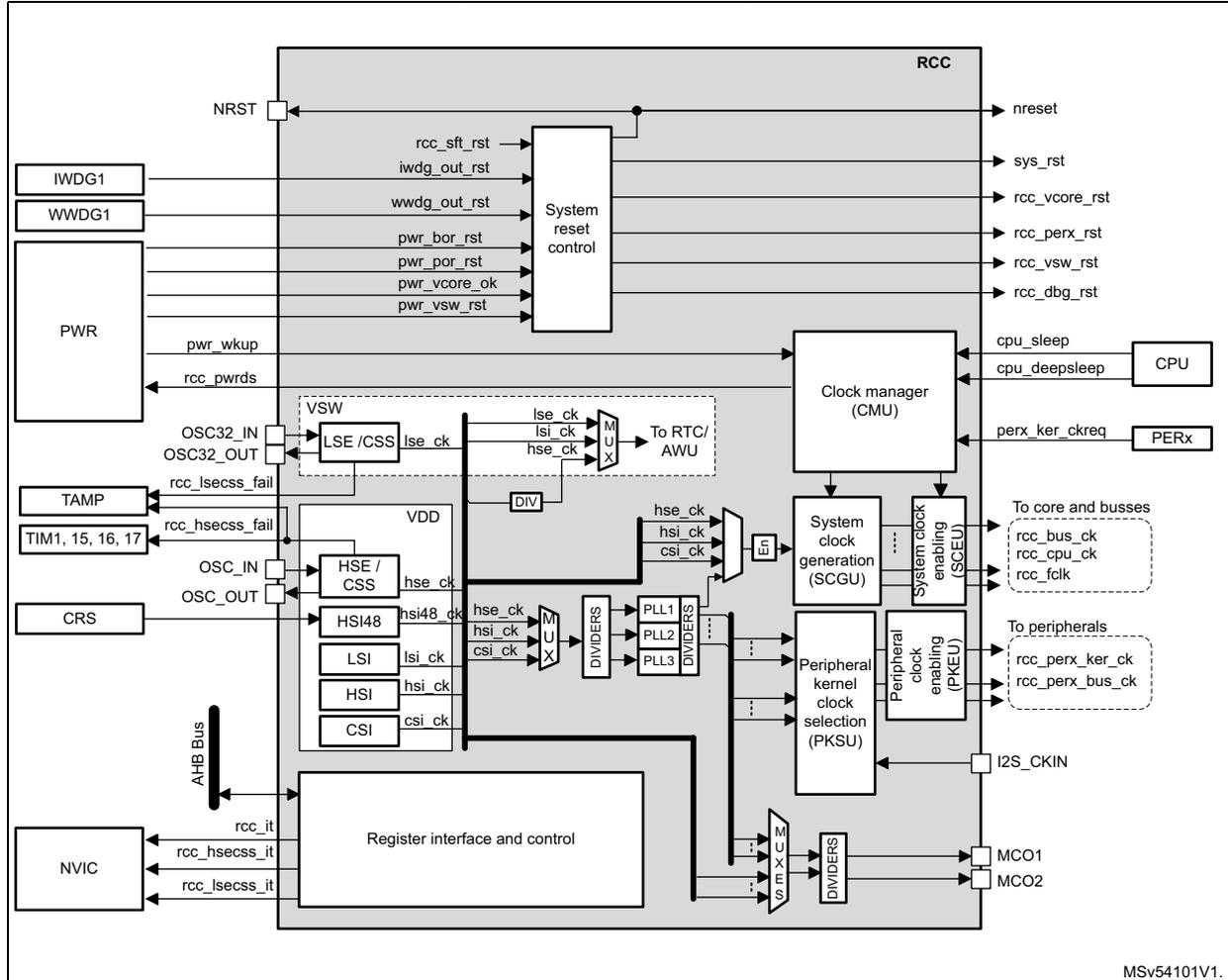
The diagram illustrates the internal architecture of the RCC block. On the left, external components are connected: IWDG1, WWDG1, and PWR (Power) to the System reset control; OSC32_IN/OUT, TAMP, TIM1, 15, 16, 17, and CRS to the VSW (Voltage Switcher) and VDD (Voltage Domain) blocks; and NVIC (Interrupt Controller) to the Register interface and control. The central part of the diagram shows the RCC internal blocks: System reset control, Clock manager (CMU), System clock generation (SCGU), Peripheral kernel clock selection (PKSU), and Register interface and control. The Register interface and control is connected to the AHB Bus and provides control signals to the other blocks. The SCGU block includes PLL1, PLL2, and PLL3 with dividers. The PKSU block includes a Peripheral clock enabling (PKEU) block. On the right, the CMU outputs nreset, sys_rst, rcc_vcore_rst, rcc_perx_rst, rcc_vsw_rst, and rcc_dbg_rst. The SCGU outputs rcc_bus_ck, rcc_cpu_ck, and rcc_fclk to the core and busses. The PKEU outputs rcc_perx_ker_ck and rcc_perx_bus_ck to the peripherals. The PKSU also outputs MCO1 and MCO2. The Register interface and control also outputs rcc_it, rcc_hsecss_it, and rcc_lsecss_it to the NVIC. The diagram is labeled MSv54101V1.
7.3 RCC pins and internal signals
Table 54 lists the RCC inputs and output signals connected to package pins or balls.
Table 54. RCC input/output signals connected to package pins or balls
| Signal name | Signal type | Description |
|---|---|---|
| NRST | I/O | System reset, can be used to provide reset to external devices |
| OSC32_IN | I | 32 kHz oscillator input |
| OSC32_OUT | O | 32 kHz oscillator output |
| OSC_IN | I | System oscillator input |
| OSC_OUT | O | System oscillator output |
| MCO1 | O | Output clock 1 for external devices |
| MCO2 | O | Output clock 2 for external devices |
| I2S_CKIN | I | External kernel clock input for digital audio interfaces: SPI/I2S, SAI, and ADF |
The RCC exchanges a lot of internal signals with all components of the product, for that reason, Table 55 only shows the most significant internal signals.
Table 55. RCC internal input/output signals
| Signal name | Signal type | Description |
|---|---|---|
| rcc_it | O | General interrupt request line |
| rcc_hsecss_it | O | HSE clock security failure interrupt |
| rcc_lsecss_it | O | LSE clock security failure interrupt |
| rcc_hsecss_fail | O | Event indicating that a HSE clock security failure is detected. This signal is connected to TIMERS. |
| rcc_lsecss_fail | O | Event indicating that a LSE clock security failure is detected. This signal is connected to TAMP, EXTI and PWR |
| nreset | I/O | Application reset |
| sys_rst | I/O | System reset |
| iwdg_out_rst | I | Reset line driven by the IWDG, indicating that a timeout occurred |
| wwdg_out_rst | I | Reset line driven by the WWDG, indicating that a timeout occurred |
| pwr_bor_rst | I | Brownout reset generated by the PWR block |
| pwr_por_rst | I | Power-on reset generated by the PWR block |
| pwr_vsw_rst | I | Power-on reset of the VSW domain generated by the PWR block |
| rcc_perx_rst | O | Reset generated by the RCC for the peripherals |
| pwr_wkup | I | Wake-up domain request generated by the PWR and used to restore the domain clocks |
| rcc_pwd_req | O | Low-power request generated by the RCC and used to set the circuit into low-power mode |
Table 55. RCC internal input/output signals (Continued)
| Signal name | Signal type | Description |
|---|---|---|
| cpu_sleep | I | Signals generated by the CPU, indicating if the CPU is in CRun, Sleep or CStop |
| cpu_deepsleep | I | |
| perx_ker_ckreq | I | Signal generated by some peripherals in order to request the activation of their kernel clock |
| rcc_perx_ker_ck | O | Kernel clock signals generated by the RCC, for some peripherals |
| rcc_perx_bus_ck | O | Bus interface clock signals generated by the RCC for peripherals |
| rcc_bus_ck | O | Clocks for APB, AHB and AXI bridges generated by the RCC |
| rcc_cpu_ck | O | Clocks for the CPU, generated by the RCC |
| rcc_fclk | O |
7.4 RCC reset block functional description
The RCC handles the reset generation for the complete product, using events coming from different sources:
- • assertion of the NRST pin from an external device
- • a failure on the supply voltage applied to VDD, VBAT
- • an exit from Standby
- • a watchdog timeout
- • a software command
The reset scope depends on the source that generates the reset.
7.4.1 Reset from PWR block
The PWR block provides several reset signals to the RCC:
- • The power-on/off reset signal ( pwr_por_rst ), which is asserted when the VDD supply is lower than the VPOR threshold.
- • The brown-out reset signal ( pwr_bor_rst ), which is asserted when the VDD supply is lower than the VBOR threshold.
- • The core reset signal ( pwr_vcore_ok ), which is asserted when the VDDCORE supply is not valid or available. Note that the VDDCORE voltage is switched off, when the product is in Standby. So when the system exits from Standby mode, the pwr_vcore_ok signal is asserted as long the VDDCORE voltage provided by the internal regulator is not valid. Note that when VDD supply is not valid, pwr_vcore_ok is asserted as well.
- • The VSW domain reset signal ( pwr_vsw_rst ), which is asserted when the VSW supply is lower than the expected threshold.
Note: The rcc_vcore_rst is generated from the pwr_vcore_ok signal, the main difference between these two signals is that rcc_vcore_rst remains asserted until the option byte loading operation is completed.
Refer to Table 56: Reset coverage summary for details.
Figure 38. Simplified reset circuit
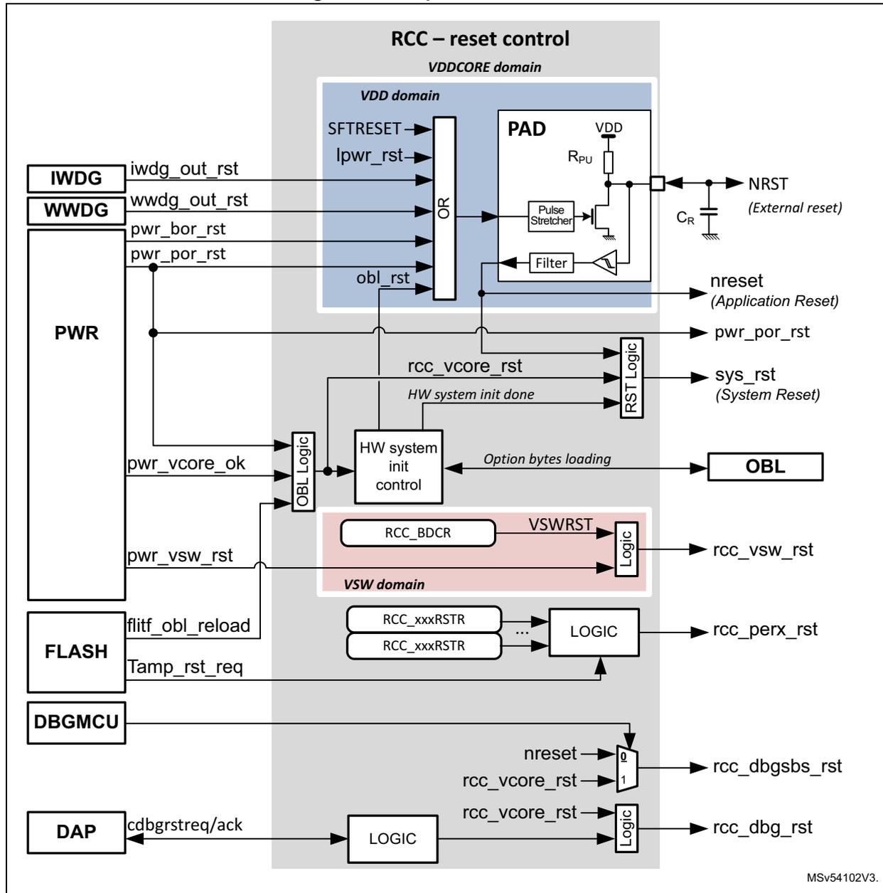
The diagram illustrates the simplified reset circuit architecture, organized into three main power domains: VDDCORE domain (grey), VDD domain (blue), and VSW domain (pink).
- External Reset (NRST): An external reset pin connected to a PAD with pull-up resistor \( R_{PU} \) and capacitor \( C_R \) . The PAD output is filtered and then stretched by a pulse stretcher.
- Internal Reset Sources:
- IWDG
(Independent Watchdog) and
WWDG
(Window Watchdog) provide
iwdg_out_rstandwwdg_out_rstsignals. - PWR
(Power) provides
pwr_bor_rst,pwr_por_rst, andpwr_vsw_rstsignals. - FLASH
provides
flitf_obl_reloadandTamp_rst_reqsignals. - DBGMCU provides a debug reset signal.
- DAP
(Debug Access Port) provides
cdbrstreq/acksignals.
- IWDG
(Independent Watchdog) and
WWDG
(Window Watchdog) provide
- Logic and Control:
- Signals from IWDG, WWDG, and the pulse stretcher are combined in an OR gate within the VDD domain.
- The output of the OR gate and
obl_rstare inputs to a PAD logic block. pwr_por_rstandrcc_vcore_rstare inputs to an RST Logic block.- A
HW system init control
block receives
pwr_vcore_ok,HW system init done, andOption bytes loadingsignals, and it controls the OBL (Option bytes loading) block. - In the VSW domain,
RCC_BDCR
provides the
VSWRSTsignal to a Logic block. - RCC_xxxRSTR
registers provide signals to a
LOGIC
block for
rcc_perx_rst. - Logic blocks combine various reset signals to generate final outputs:
nreset(Application Reset),pwr_por_rst,sys_rst(System Reset),rcc_vsw_rst,rcc_perx_rst,rcc_dbgbs_rst, andrcc_dbg_rst.
MSV54102V3.
7.4.2 The system and application resets (sys_rst and nreset)
A system reset ( sys_rst ) resets most of the registers to their default values unless otherwise specified in the register description.
A system reset can be generated from one of the following sources:
- • an assertion of the NRST pin (external reset)
- • a reset from the power-on/off reset block ( pwr_por_rst )
- • a reset from the brownout reset block (
pwr_bor_rst
)
Refer to Section 6.5.2: Brownout reset (BOR) for a detailed description of the BOR function. - • a reset from the independent watchdogs ( iwdg_out_rst )
- • an exit from Standby ( rcc_vcore_rst ).
- • a reset from the window watchdogs depending on WWDG configuration ( wwdg_out_rst )
- • a software reset from the Cortex®-M7 core
It is generated via the SYSRESETREQ signal issued by the Cortex®-M7 core. This signal is also named SFTRESET in this document. - • A reset from the low-power mode security reset, depending on option byte configuration ( lpwr_rst ).
- • An option byte reload request from the flash interface ( obl_rst )
The application reset ( nreset ) is similar to the system reset, but is not asserted when the system exits from Standby.
Note: The SYSRESETREQ bit in Cortex®-M7 through the FPU application interrupt and reset control register, must be set to force a software reset on the device. Refer to the Cortex®-M7 with FPU technical reference manual for more details (see http://infocenter.arm.com ).
7.4.3 The NRST reset
The NRST is active low. A pulse stretcher guarantees a minimum reset pulse duration of 20 µs (Refer to datasheet for details). In addition it is possible to extend the NRST assertion thanks to \( C_R \) capacitor. It is not recommended to let the NRST pin unconnected.
When it is not used, connect this pin to ground via a 10 to 100 nF capacitor (CR in Figure 38 ). As shown in Figure 38 , a filter is also present in order to suppress spurs coming from NRST PAD.
7.4.4 Low-power mode security reset (lpwr_rst)
To prevent critical applications from mistakenly enter a low-power mode, two low-power mode security resets are available. When enabled through nRST_STOP and nRST_STANDBY option bytes, a system reset is generated if the following conditions are met:
- • The CPU accidentally enters Stop mode.
This type of reset is enabled by resetting nRST_STOP user option byte. In this case, whenever the Stop mode entry sequence is successfully executed, a system reset is generated. - • The system accidentally enter Standby mode.
This type of reset is enabled by resetting nRST_STANDBY user option byte. In this
case, whenever a Standby mode entry sequence is successfully executed, a system reset is generated.
When the Standby mode is entered, a flag is also set in the power controller.
LPWRRSTF bit in the RCC Reset status register (RCC_RSR) indicates that a low-power mode security reset occurred (see line #7 in Table 57 ).
lpwr_rst is activated when a low-power mode security reset due to CPU occurred.
Refer to Section 5.4: FLASH option bytes for additional information.
Refer to Section 6: Power control (PWR) for additional information and Table 45: Operating mode summary for the overview of the existing power modes.
7.4.5 Backup domain reset
A backup domain reset ( pwr_vsw_rst ) is generated when one of the following events occurs:
- • Software reset, triggered by setting the VSWRST bit in the RCC Backup domain control register (RCC_BDCR) . All RTC registers and the RCC_BDCR register are set to their reset values, with the exception of LSEDRV, which is not changed if LSEON=1. The BKPSRAM is not affected.
- • When the VSW voltage is outside the operating range. All RTC registers and the RCC_BDCR register are set to their reset values. In this case the content of the BKPSRAM is no longer valid.
Refer to Section 6.4.4: Backup domain section of PWR block and to section “ System security ” for additional information.
7.4.6 Coresight debug reset
The coresight debug components can be reset in different ways:
- • Over the DAP by setting to 1 the bit CDBGIRSTREQ of the control/status register of the debug port. This action asserts the debug reset request signal cdbgirstreq connected to the RCC. Then the RCC activates the debug reset ( rcc_dbg_rst ), a handshake signal cdbgirstack is provided to the DAP request. The debug reset remains as long as the cdbgirstreq is to 1, refer to Figure 38 for details.
- • When VDDCORE power-on reset occurs ( rcc_vcore_rst ). This reset is activated after a power-on reset, or when the product exits from Standby.
Refer to Section 1.7.1: CoreSight Debug Reset for details.
7.4.7 Option bytes loading
As shown in Figure 38 , the option bytes loading (OBL) sequence is triggered under the following conditions:
- • After a power-on, or
- • When the system exits from Standby
- • When the flash interface requested a reload of option bytes
The system reset ( sys_rst ) can be released only when the option byte loading (OBL) is completed.
7.4.8 Peripheral resets
The application can individually reset any peripheral whenever requested. This can be done via the RCC_xxxxRSTR registers where “xxxx” is the name of the bus to which the peripheral is connected.
In order to reset a peripheral, the corresponding reset bit must be set to 1, and then set back to 0. There is no need to enable the peripheral clock in order to reset a peripheral.
Note also that the CRYPT, SAES and HASH blocks can be reset in the case of a tamper event.
7.4.9 Reset coverage summary
Table 56: Reset coverage summary gives a detailed view of the reset coverage of the most important reset sources.
Note: When \( V_{DD} \) is not valid, \( V_{DDCORE} \) is also not valid.
Table 56. Reset coverage summary (1)| Functions that are reset | Main reset lines | |||||||
|---|---|---|---|---|---|---|---|---|
| pwr_por_rst (2) | rcc_vcore_rst | sys_rst | nreset (4) | rcc_dbg_rst | rcc_perx_rst | rcc_vsw_rst | ||
| VDD domain | X | - | - | - | - | - | - | |
| MCU | X | X | X | - | - | - | - | |
| WWDG | X | X | X | - | - | - | - | |
| IWDG | X | - | - | X | - | - | - | |
| AXI/AHB Interconnections. | X | X | X | - | - | - | - | |
| Debug components, including DBGMCU Reset all the debug parts except the SWJ-DP function. The SWJ-DP is reset by the NJTRST or rcc_vcore_rst resets. The bit DCRT on DBGMCU_CR is reset with pwr_por_rst. | X | X | - | - | X | - | - | |
| Hardware system init. It includes the reload of the option bytes. | X | X | - | - | - | - | - | |
| RCC | RCC Reset status register (RCC_RSR) | X | - | - | - | - | - | - |
| RCC clock control and status register (RCC_CSR) | X | - | - | - | - | - | - | |
| RCC Backup domain control register (RCC_BDCR) | - | - | - | - | - | - | X | |
| Other RCC registers | X | X | X | - | - | - | - | |
| PWR | PWR_CSR1 | - | - | - | - | - | - | X |
| PWR_CSR2 | X | - | - | - | - | - | - | |
| PWR_CSR3 Individual bits of this register do not have the same reset condition, refer to the PWR section for details. | X | X | X | - | - | - | - | |
| PWR_WKUPCR, PWR_WKUPFR, PWR_WKUPEPR | X | - | - | X | - | - | - | |
| Other registers | X | X | X | - | - | - | - | |
| RTC | - | - | - | - | - | - | X | |
| BKPSRAM After a reset of the VSW domain, the backup regulator of the BKPSRAM is disabled, this function is controlled via the PWR block, BREN bit. If the rcc_vsw_rst reset is due to a too low VSW voltage, the content of BKPSRAM is lost. | - | - | - | - | - | - | X | |
| SBS | SBS_RSSCMR | X | - | - | - | - | - | - |
| Other Peripherals | X | X | X | - | - | X | - | |
1. The 'X' means that the function is reset by the corresponding reset line, the '-' means that the function is not reset by the corresponding reset line.
2. The pwr_por_rst is asserted when the voltage applied to VDD is not valid.
When pwr_por_rst is asserted, the rcc_vcore_rst, NRST, the sys_rst and the nreset, are asserted as well.
- 3. The
rcc_vcore_rstis asserted when the voltage applied to VDD is not valid, or when the system exits from Standby (because VDDCORE was switched off).
Whenrcc_vcore_rstis asserted, thesys_rst, and thepwr_dbg_rstare asserted as well. - 4. When nreset is asserted, the
sys_rstis also asserted.
7.4.10 Reset source identification
The CPU can identify the reset source by checking the reset flags in the
RCC_RSR
register.
The CPU can reset the flags by setting RMVF bit.
Table 57
shows how the status bits of the
RCC_RSR
register behave according to the situation that generated the reset. For example, when an IWDG timeout occurs (line #6), if the CPU is reading the
RCC_RSR
register during the boot phase, both PINRSTF and IWDGRSTF bits are set, indicating that the IWDG also generated a pin reset.
Table 57. Reset source identification (RCC_RSR) (1)
| # | Situations generating a reset | SBF (2) | LPWRRSTF | WWDGRSTF | IWDGRSTF | SFTRSTF | PORRSTF | PINRSTF | BORRSTF | OBLRSTF |
|---|---|---|---|---|---|---|---|---|---|---|
| 1 | Power-on reset ( pwr_por_rst ) | 0 | 0 | 0 | 0 | 0 | 1 | 1 | 1 | 0 |
| 2 | Pin reset (NRST) | 0 | 0 | 0 | 0 | 0 | 0 | 1 | 0 | 0 |
| 3 | Brownout reset ( pwr_bor_rst ) | 0 | 0 | 0 | 0 | 0 | 0 | 1 | 1 | 0 |
| 4 | System reset generated by CPU (SFTRESET) | 0 | 0 | 0 | 0 | 1 | 0 | 1 | 0 | 0 |
| 5 | WWDG reset ( wwdg_out_rst ) | 0 | 0 | 1 | 0 | 0 | 0 | 1 | 0 | 0 |
| 6 | IWDG reset ( iwdg_out_rst ) | 0 | 0 | 0 | 1 | 0 | 0 | 1 | 0 | 0 |
| 7 | CPU erroneously enters Stop or Standby mode | 0 | 1 | 0 | 0 | 0 | 0 | 1 | 0 | 0 |
| 8 | The flash interface requested a reload of option bytes | 0 | 0 | 0 | 0 | 0 | 0 | 1 | 0 | 1 |
| 9 | The product exits from Standby | 1 | 0 | 0 | 0 | 0 | 0 | 1 | 0 | 0 |
- 1. Grayed cells highlight the register bits that are set.
- 2. The SBF bit is located into the
PWR_CSR3register of the PWR block
7.4.11 Power-on and wake-up sequences
For detailed diagrams refer to Section 6.4.1: System supply startup in the PWR section.
The time interval between the event that exits the product from a low-power and the moment where the CPU is able to execute code, depends on the system state and on its configuration. Figure 39 shows the most usual examples.
Power-on wake-up sequence
The power-on wake-up sequence shown in Figure 39 gives the most significant phases of the power-on sequence. It is the longest sequence since the circuit was not powered. Note that this sequence remains unchanged, whatever \( V_{BAT} \) was present or not.
Boot from pin reset
When a pin reset occurs, V DD is still present. As a result:
- • The regulator settling time is faster since the reference voltage is already stable.
- • The HSI restart delay may be needed if the HSI was not enabled when the NRST occurred, otherwise this restart delay phase is skipped.
- • The Flash memory power recovery delay can also be skipped if the Flash memory was enabled when the NRST occurred.
Note: The boot sequence is similar for pwr_bor_rst, lpwr_rst, STFRESET, iwdg_out_rst and wwdg_out_rst.
Boot from system Standby
When waking up from system Standby, the reference voltage is stable since V DD has not been removed. As a result, the regulator settling time is fast. Since V CORE was not present, the restart delay for the HSI, the Flash memory power recovery and the option byte reloading cannot be skipped.
Restart from system Stop
When restarting from Stop, V DD is still present. As a result, the sequence is mainly composed of two steps:
- 1. Regulator settling time to reach VOS low (default voltage).
- 2. HSI/CSI restart delay. This step can be skipped if HSIKERON or CSIKERON bit is set to 1 in the RCC register map .
Figure 39. Boot sequences versus system states
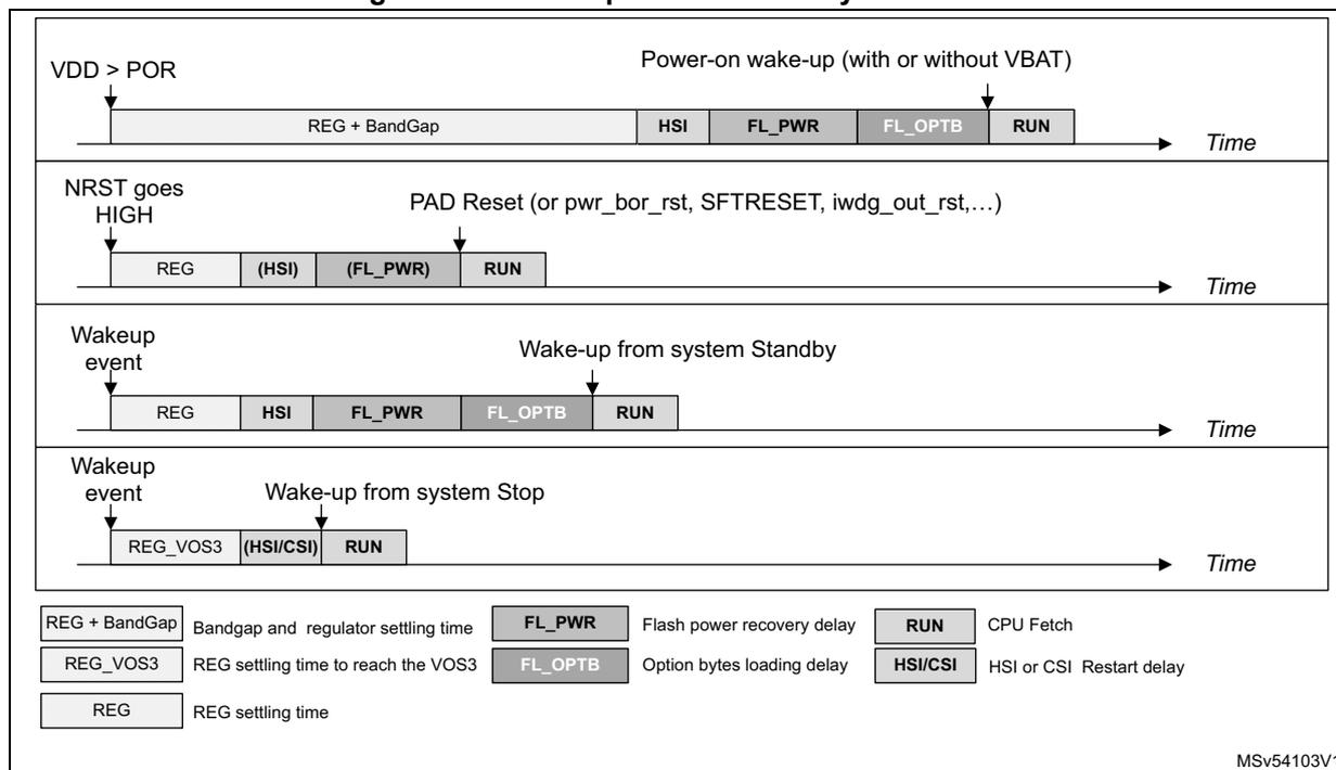
The figure displays four horizontal timelines representing boot sequences over time for different system states:
- Power-on wake-up (with or without VBAT): Triggered by V DD > POR. The sequence includes: REG + BandGap, HSI, FL_PWR, FL_OPTB, and RUN.
- PAD Reset (or pwr_bor_rst, STFRESET, iwdg_out_rst,...): Triggered when NRST goes HIGH. The sequence includes: REG, (HSI), (FL_PWR), and RUN. Parentheses indicate optional or skipped phases.
- Wake-up from system Standby: Triggered by a wakeup event. The sequence includes: REG, HSI, FL_PWR, FL_OPTB, and RUN.
- Wake-up from system Stop: Triggered by a wakeup event. The sequence includes: REG_VOS3, (HSI/CSI), and RUN.
Legend:
| REG + BandGap | Bandgap and regulator settling time | FL_PWR | Flash power recovery delay | RUN | CPU Fetch |
| REG_VOS3 | REG settling time to reach the VOS3 | FL_OPTB | Option bytes loading delay | HSI/CSI | HSI or CSI Restart delay |
| REG | REG settling time | ||||
MSv54103V1
7.5 RCC clock block functional description
The RCC provides a wide choice of clock generators:
- • HSI (high-speed internal oscillator) clock: ~ 8, 16, 32 or 64 MHz
- • HSE (high-speed external oscillator) clock: 4 to 50 MHz
- • LSE (low-speed external oscillator) clock: 32 kHz
- • LSI (low-speed internal oscillator) clock: ~ 32 kHz
- • CSI (low-power internal oscillator) clock: ~4 MHz
- • HSI48 (high-speed internal oscillator) clock: ~48 MHz
The RCC offers a high flexibility for the application to select the appropriate clock for CPU and peripherals, in particular for peripherals that require a specific clock such as SPI/I2S and SAI.
To optimize the power consumption, each clock source can be switched ON or OFF independently.
The RCC provides up to 3 PLLs; each of them can be configured in integer, with or without SSCG, or fractional mode.
As shown in the Figure 40 , the RCC offers two clock outputs (MCO1 and MCO2), with a great flexibility on the clock selection and frequency adjustment.
The SCGU block (system clock generation unit) contains several prescalers used to configure the CPU and bus matrix clock frequencies.
The PKSU block (peripheral kernel clock selection unit) provides several dynamic switches allowing a large choice of kernel clock distribution to peripherals.
The PKEU (peripheral kernel clock enable unit) and SCEU (system clock enable unit) blocks perform the peripheral kernel clock gating, and the bus interface/cores/bus matrix clock gating, respectively.
Figure 40. Top-level clock tree
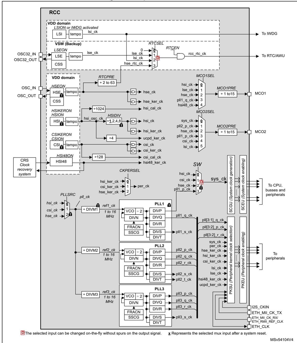
The diagram illustrates the top-level clock tree for the RCC. It shows the following components and paths:
- RCC Domain:
- VDD domain: LSI (LSION or IWDG activated) provides lsi_ck to IWDG.
- VSW (Backup): OSC32_IN/OSC32_OUT (LSE, CSS) provides lse_ck. RTCSEL selects between lse_ck, lsi_ck, and hse_rtc_ck for the RTC/AWU via RTCCEN.
- VDD domain (Main):
- OSC_IN/OSC_OUT (HSE, CSS) provides hse_ck, hse_ker_ck, and hse_cal_ck.
- HSI (HSION, HSIKERON) provides hsi_osc_ck, which is divided by HSI48ON (+128) for hsi48_ker_ck and by HSI48ON (+128) for hsi_cal_ck. HSI also provides hsi_ck and hsi_ker_ck.
- CSI (CSION, CSIKERON) provides csi_osc_ck, which is divided by CSIDIV (+1,2,4,8) for csi_ck and csi_ker_ck, and by CSIDIV (+4) for ucpd_ker_ck.
- CRS Clock recovery system provides input to HSI48ON.
- MCUs:
- MCO1: MCO1SEL selects between hsi_ck, lse_ck, hse_ck, pll1_q_ck, and hsi48_ck. MCO1PRE (+1 to 15) provides the output.
- MCO2: MCO2SEL selects between sys_ck, pll2_p_ck, hse_ck, pll1_p_ck, csi_ck, and lsi_ck. MCO2PRE (+1 to 15) provides the output.
- PLLs:
- PLL1: PLLSRC selects between hsi_ck, csi_ck, and hse_ck. PLL1 includes VCO, DIVP, DIVN, DIVQ, DIVR, FRACN, SSGC, and DIVT. Outputs: pll1_q_ck, pll1_s_ck, and pll1_p_ck.
- PLL2: ref2_ck (from +DIVM2, 1 to 16 MHz) is the input. PLL2 includes VCO, DIVP, DIVN, DIVQ, DIVR, FRACN, SSGC, and DIVT. Outputs: pll2_p_ck, pll2_q_ck, pll2_r_ck, pll2_s_ck, and pll2_t_ck.
- PLL3: ref3_ck (from +DIVM3, 1 to 16 MHz) is the input. PLL3 includes VCO, DIVP, DIVN, DIVQ, DIVR, FRACN, SSGC, and DIVT. Outputs: pll3_p_ck, pll3_q_ck, pll3_r_ck, and pll3_s_ck.
- System Clock (sys_ck): SW selects between hsi_ck, csi_ck, hse_ck, and pll1_p_ck. sys_ck is distributed to CPU, busses, and peripherals via SCGU (System clock generation) and SCEU (System clock enabling).
- Peripheral Clocks:
- per_ck: CKPERSEL selects between hsi_ker_ck, csi_ker_ck, and hse_ker_ck.
- PKSU (Peripheral kernel clock selection) provides clocks to peripherals via PKEU (Peripheral clock enabling). Inputs include sys_ck, per_ck, hse_ker_ck, hsi_ker_ck, csi_ker_ck, lsi_ck, lse_ck, hsi48_ker_ck, and ucpd_ker_ck. Outputs include I2S_CKIN, ETH_MII_CK_TX, ETH_MII_CK_RX, ETH_RMII_REF_CLK, and ETH_CLK.
D The selected input can be changed on-the-fly without spurs on the output signal. x Represents the selected mux input after a system reset.
MSV54104V4
7.5.1 Clock naming convention
The RCC provides clocks to the complete circuit. To avoid misunderstanding, the following terms are used in this document:
- • Peripheral clocks
The peripheral clocks are the clocks provided by the RCC to the peripherals. Two kinds of clock are available:
- – bus interface clocks
- – kernel clocks
A peripheral receives from the RCC a bus interface clock in order to access its registers, and thus control the peripheral operation. This clock is generally the AHB, APB or AXI clock depending on which bus the peripheral is connected to. Some peripherals only need a bus interface clock (such as RNG, TIMx).
Some peripherals also require a dedicated clock to handle the interface function. This clock is named kernel clock. As an example, peripherals such as SAI must generate specific and accurate master clock frequencies, which require dedicated kernel clock frequencies. Another advantage of decoupling the bus interface clock from the specific interface needs, is that the bus clock can be changed without reprogramming the peripheral.
- • CPU clock
The CPU clock is the clock provided to the CPU. It is derived from the system clock ( sys_ck ).
- • Bus matrix clocks
The bus matrix clocks are the clocks provided to the different bridges (APB, AHB or AXI). These clocks are derived from the system clock ( sys_ck ).
7.5.2 Oscillators description
The table hereafter shows the oscillator states versus system modes, when the oscillators are enabled via registers. The term “available” means that the resource can be used if activated via registers.
Table 58. Oscillator states versus system modes
| System modes | VDD domain | VSW domain | ||||
|---|---|---|---|---|---|---|
| HSE | HSI | HSI48 | CSI | LSI | LSE | |
| Exit from system reset | OFF | ON | OFF | OFF | Available | Available |
| Exit from system Stop | OFF | ON (1) | OFF | ON (2) | Available | Available |
| In Run/Sleep | Available | Available | Available | Available | Available | Available |
| In Stop | OFF | Available (3) | OFF | Available (4) | Available | Available |
| In Standby | OFF | OFF | OFF | OFF | Available | Available |
| In VBAT | OFF | OFF | OFF | OFF | OFF | Available |
1. If STOPWUCK = 0 or STOPKERWUCK = 0
2. If STOPWUCK = 1 or STOPKERWUCK = 1
3. HSI can remain activated in Stop if HSIKERON = 1, or if a peripheral selecting HSI, generates a kernel clock request.
4. CSI can remain activated in Stop if CSIKERON = 1, or if the peripheral selecting CSI, generates a kernel clock request.
HSE oscillator
The HSE block allows the application to provide a very accurate high-speed clock for the product. The HSE can generate an internal clock from two possible sources:
- • external clock source
- • external crystal/ceramic resonator
Figure 41. HSE/LSE clock source
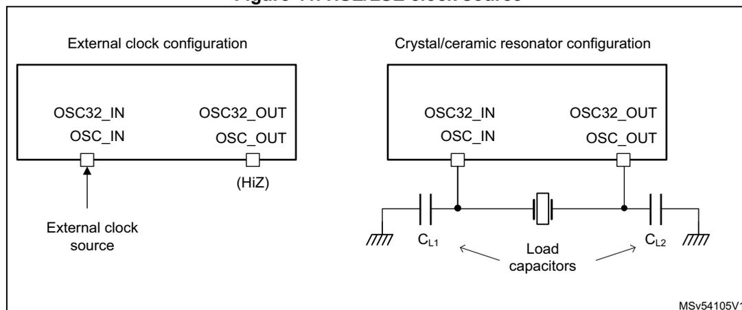
External clock source (HSE bypass)
In this mode the oscillator is not used, and an external clock source must be provided to OSC_IN pin. The external clock can be low swing (analog) or digital. The OSC_OUT pin must be left HI-Z (see Figure 41).
The external clock signal can be digital or analog (square, sinus or triangle). An analog clock signal with a reduced amplitude, is supported thanks to an internal clock squarer. The input signal must have a duty cycle close to 50%. Refer to the datasheet for additional information.
This mode is selected when HSEBYP = 1, and HSEON = 1. In case of an analog clock input (low swing) the HSEEXT must be set to 0, for a digital clock input, HSEEXT bits must be set to 1.
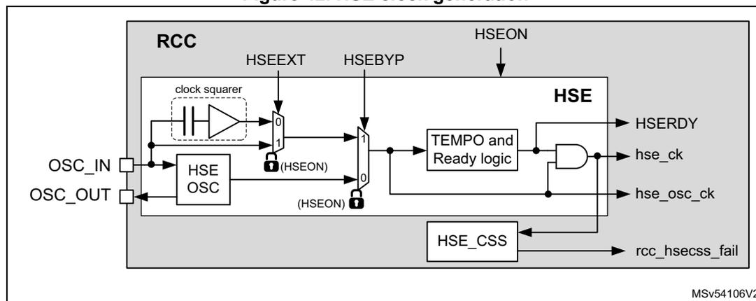
Figure 42. HSE clock generation
External crystal/ceramic resonator
A crystal/resonator can be connected as shown in Figure 41 : the crystal/resonator and the load capacitors must be placed as close as possible to the oscillator pins in order to minimize output distortion and startup stabilization time. The loading capacitance values must be adjusted according to the selected crystal or ceramic resonator. Refer to the electrical characteristics section of the datasheet for more details.
The oscillator mode is enabled by setting the HSEBYP bit to 0 and HSEON bit to 1.
HSE ready logic
The HSERDY flag indicates when a valid clock is available at HSE output ( hse_ck ). When the HSE is enabled (HSEON set to '1'), the HSERDY flag goes to '1' when 256 valid cycles of HSE have been detected. The hse_ck clock is not released until HSERDY goes to 1.
An interrupt can be generated if enabled in the RCC clock source interrupt enable register (RCC_CIER) .
HSE controls
The HSE can be switched ON and OFF through the HSEON bit.
The hardware does not allow modifying HSEON bit if one of the condition is met:
- • The HSE is used directly (via SW switch) as system clock.
- • The HSE is selected as reference clock for PLL1, with PLL1 enabled and selected to provide the system clock (via SW switch).
- • The bit XSPICKP is set to 1.
- • The bit FMCKP is set to 1.
The hardware does not allow changing the values of HSEBYP, and HSEEXT when HSEON = 1. Bits HSEBYP, HSEEXT and HSEON are located into the RCC register map .
The HSE is automatically disabled by hardware when the system enters Stop or Standby mode (See Table 58: Oscillator states versus system modes ).
In addition, the HSE clock can be driven to the MCO1 and MCO2 outputs and used as clock source for other application components.
Programming sequence
In order initialize the HSE, the application must follow the sequence hereafter:
- • Make sure the HSE is not directly or indirectly used as system clock, if it is the case, use HSI or CSI as clock source for system clock.
- • Make sure that XSPICKP and FMCCKP are set to 0
- • Disable the HSE by writing to 0 the HSEON bit,
- • Check that the HSE is disabled by waiting that the bit HSERDY is set to 0,
- • If the oscillator mode is needed:
- – Select the oscillator mode by setting HSEBYP to 0,
- • If an external clock is connected to OSC_IN:
- – Select the bypass mode by setting HSEBYP to 1,
- – If the input clock is a full-swing digital signal, set HSEEXT to 1
- – If the input clock is a low-swing signal, set HSEEXT to 0
- • Enable again the HSE by writing the HSEON bit to 1,
- • Wait for HSERDY = 1, then the HSE is ready for use.
LSE oscillator
The LSE block allows the application to provide a very accurate low-frequency clock for the product. The LSE can generate an internal clock from two possible sources:
- • external user clock
- • external crystal/ceramic resonator
External clock source (LSE bypass)
In this mode, the oscillator is not used, and an external clock source must be provided to OSC32_IN pin. The OSC32_OUT pin must be left HI-Z (see Figure 41 ).
The external clock signal can have a frequency up to 1 MHz and be digital or analog (square, sinus or triangle). An analog clock signal with a reduced amplitude, is supported thanks to an internal clock squarer. The input signal must have a duty cycle close to 50%. Refer to the datasheet for additional information.
This mode is selected by setting the LSEBYP and LSEON bits to 1. In case of an analog clock input (low swing) the LSEEXT must be set to 0, for a digital clock input, LSEEXT bits must be set to 1.
Figure 43. LSE clock generation
![Figure 43. LSE clock generation block diagram. The diagram shows the internal architecture of the LSE block within the RCC. It includes an LSE OSC (Low-Speed External Oscillator) connected to OSC32_IN and OSC32_OUT pins. The OSC32_IN pin is also connected to a clock squarer. The LSE OSC output is connected to a multiplexer (MUX) labeled LSEEXT. The MUX has two inputs: one from the clock squarer (labeled 0) and one from the LSE OSC (labeled 1). The MUX output is connected to the LSE block. The LSE block contains a TEMPO and Ready logic block, which is also connected to the LSEON bit. The LSE block outputs LSECK and LSERDY. The LSECK output is connected to the LSE_CSS block, which in turn outputs rcc_lsecs_fail. The LSE block is also connected to the LSEDRV[1:0] register. The LSEON bit is connected to the LSE block and the TEMPO and Ready logic block. The LSEEXT bit is connected to the MUX. The LSEBYP bit is connected to the MUX. The LSEON bit is also connected to the LSE block. The LSE block is labeled Vsw domain. The diagram is labeled MSV54107V2.](/RM0477-STM32H7Rx-7Sx/922cbd842837181a486c2aceb2b6cd65_img.jpg)
External crystal/ceramic resonator source (LSE crystal)
The LSE clock is generated from a 32.768 kHz crystal or ceramic resonator. It has the advantage to provide a low-power highly accurate clock source to the real-time clock (RTC) for clock/calendar or other timing functions. A crystal/resonator can be connected as shown in Figure 41 : the crystal/resonator and the load capacitors must be placed as close as possible to the oscillator pins in order to minimize output distortion and startup stabilization time. The loading capacitance values must be adjusted according to the selected crystal or ceramic resonator. Refer to the electrical characteristics section of the datasheet for more details.
The oscillator mode is selected by setting LSEBYP bit to 0 and LSEON bit to 1.
The LSE also offers a programmable driving capability (LSEDRV[1:0]) that can be used to modulate the amplifier driving capability. This driving capability is chosen according to the external crystal/ceramic component requirement to insure a stable oscillation.
The driving capability must be set before enabling the LSE oscillator.
Warning: It is not allowed to change the driving capability when the LSE is enabled. The LSE behavior is not guaranteed in that case.
LSE ready logic
The LSE offers a LSERDY flag which indicates whether the LSE clock is available or not. When the LSE is enabled (LSEON set to 1) the LSERDY flag goes to 1 when certain amount of valid cycles of LSE clock have been detected. The lse_ck clock is not released until LSERDY goes to 1.
When LSEBYP = 0, the RCC waits 4096 clocks cycles before activating the LSERDY flag, when LSEBYP = 1, the RCC waits 8 clocks cycles.
An interrupt, can be generated if enabled in the RCC clock source interrupt enable register (RCC_CIER) .
LSERDY bit is located into the RCC Backup domain control register (RCC_BDCR) .
LSE controls
The LSE control bits LSEBYP, LSEEXT, LSEDRV[1:0] and LSEON are located into the RCC Backup domain control register (RCC_BDCR) . This register is write-protected by DBP bit of PWR_CR1 register. In order to modify the RCC_BDCR register, the bit DBP must be set 1.
The LSE oscillator is switched ON and OFF using the LSEON bit.
The LSE remains enabled when the system enters Stop, Standby or VBAT mode (See Table 58: Oscillator states versus system modes ).
The hardware does not allow changing the values of LSEBYP, and LSEEXT when LSEON = 1.
In addition, the LSE clock can be driven to the MCO1 output and used as clock source for external components.
LSE Programming sequence
In order initialize the LSE, the application must follow the sequence hereafter:
- • Set DBP bit of PWR_CR1 to 1 in order to allow write accesses to RCC_BDCR register.
- • Disable the LSE by writing to 0 the LSEON bit,
- • Check that the LSE is disabled by waiting that the bit LSERDY is set to 0,
- • if the oscillator mode is needed:
- – Select the oscillator mode by setting LSEBYP to 0,
- – Configure LSEDRV[1:0],
- • if an external clock is connected to OSC32_IN:
- – Select the bypass mode by setting LSEBYP to 1,
- – If the input clock is a full-swing digital signal, set LSEEXT to 1
- – If the input clock is a low-swing signal, set LSEEXT to 0
- • Enable again the LSE by writing the LSEON bit to 1,
- • Wait for LSERDY = 1, then the LSE is ready for use.
- • If RCC_BDCR register no longer need to be changed, set DBP bit of PWR_CR1 to 0 in order to write-protect accesses.
If the RTC is used, the LSE bypass must not be configured in digital mode but in low swing analog mode (default value after reset).
HSI oscillator
The HSI block provides the default clock to the product.
The HSI is a high-speed internal RC oscillator that can be used directly as system clock, peripheral clock, or as PLL input. A predivider allows the application to select an HSI output frequency of 8, 16, 32 or 64 MHz. This predivider is controlled by the HSIDIV.
The HSI advantages are the following:
- • low-cost clock source since no external crystal is required
- • faster startup time than HSE (a few microseconds)
The HSI frequency, even with frequency calibration, is less accurate than an external crystal oscillator or ceramic resonator.
HSI controls
The HSI can be switched ON and OFF using the HSION bit.
The hardware does not allow modifying HSION bit if one of the condition is met:
- • The HSI is used directly (via software mux) as system clock.
- • The HSI is selected as reference clock for PLL1, with PLL1 enabled and selected to provide the system clock (via software mux).
- • The bit XSPICKP is set to 1.
- • The bit FMCCPK is set to 1.
Note that the HSIDIV cannot be changed if the HSI is selected as reference clock for at least one enabled PLL (PLLxON bit set to 1). In that case the hardware does not update the HSIDIV with the new value. However it is possible to change the HSIDIV if the HSI is used directly as system clock.
The HSIRDY flag indicates if the HSI is stable or not. At startup, the HSI output clock is not released until this bit is set by hardware.
The HSI clock can also be used as a backup source (auxiliary clock) if the HSE fails (refer to Section : CSS on HSE ).
The HSI can be disabled or not when the system enters Stop mode (See Table 58: Oscillator states versus system modes ).
In addition, the HSI clock can be driven to the MCO1 output and used as clock source for other application components.
Care must be taken when the HSI is used as kernel clock for communication peripherals, the application must take into account the following parameters:
- • the time interval between the moment where the peripheral generates a kernel clock request and the moment where the clock is really available,
- • the frequency accuracy.
HSION, HSIRDY and HSIDIV bits are located in the RCC register map .
HSI calibration
RC oscillator frequencies can vary from one chip to another due to manufacturing process variations. That is why each device is factory calibrated by STMicroelectronics to achieve an accuracy of ACC HSI (refer to the product datasheet for more information).
After a power-on reset, or at the exit of Standby mode, the factory calibration value is loaded in the HSICAL[11:0] bits.
If the application is subject to voltage or temperature variations, this may affect the RC oscillator frequency. The user application can trim the HSI frequency using the HSITRIM[6:0] bits.
Note: HSICAL[11:0] and HSITRIM[6:0] bits are located in the RCC HSI calibration register (RCC_HSICFGR) .
Figure 44. HSI calibration flow
![Figure 44. HSI calibration flow diagram. The diagram shows the flow of calibration data from Engineering option bytes (factory calibration) through the RCC block to the HSI block. The RCC block contains FLASH_HSI_opt[11:9] and FLASH_HSI_opt[8:0] registers. The FLASH_HSI_opt[8:0] register is connected to an adder (+) which also receives input from the HSITRIM[6:0] (unsigned) register. The output of the adder is connected to the HSI block's CAL[11:0] register. The HSI block also contains the HSICAL[11:9] and HSICAL[8:0] registers, which are connected to the RCC_HSICFGR register. The RCC_HSICFGR register is connected to the HSI block's CAL[11:0] register. The diagram is labeled MSV48151V2.](/RM0477-STM32H7Rx-7Sx/b38817d867550ae783546d5910d4db22_img.jpg)
CSI oscillator
The CSI is a low-power RC oscillator that can be used directly as system clock, peripheral clock, or PLL input.
The CSI advantages are the following:
- • low-cost clock source since no external crystal is required
- • faster startup time than HSE (a few microseconds)
- • very low-power consumption.
The CSI provides a clock frequency of about 4 MHz, while the HSI is able to provide a clock up to 64 MHz.
CSI frequency, even with frequency calibration, is less accurate than an external crystal oscillator or ceramic resonator.
CSI controls
The CSI can be switched ON and OFF through the CSION bit. The CSIRDY flag indicates whether the CSI is stable or not. At startup, the CSI output clock is not released until this bit is set by hardware.
The hardware does not allow modifying CSION bit if one of the condition is met:
- • The CSI is used directly (via software mux) as system clock.
- • The CSI is selected as reference clock for PLL1, with PLL1 enabled and selected to provide the system clock (via software mux).
- • The bit XSPICKP is set to 1.
- • The bit FMCCPK is set to 1.
The CSI can be disabled or not when the system enters Stop mode (See Table 58: Oscillator states versus system modes ).
In addition, the CSI clock can be driven to the MCO2 output and used as clock source for other application components.
Even if the CSI settling time is faster than the HSI, care must be taken when the CSI is used as kernel clock for communication peripherals: the application must take into account the following parameters:
- • the time interval between the moment where the peripheral generates a kernel clock request and the moment where the clock is really available,
- • the frequency precision.
Note: CSION and CSIRDY bits are located in the RCC register map .
CSI calibration
RC oscillator frequencies can vary from one chip to another due to manufacturing process variations, this is why each device is factory calibrated by STMicroelectronics to achieve accuracy of ACC CSI (refer to the product datasheet for more information).
After a power-on reset, or at the exit of Standby mode, the factory calibration value is loaded in the CSICAL[7:0] bits.
If the application is subject to voltage or temperature variations, this may affect the RC oscillator frequency. The user application can trim the CSI frequency using the CSITRIM[5:0] bits.
Note: Bits CSICAL[7:0] and CSITRIM[5:0] are located into the RCC CSI calibration register (RCC_CSICFGR)
Figure 45. CSI calibration flow
![Figure 45: CSI calibration flow diagram. An external block 'Engineering option bytes (factory calibration)' provides 'FLASH_CSI_opt[7:0]' to a summation node (+) inside the RCC block. The summation node also receives 'CSITRIM[5:0] (unsigned)' from the 'RCC_CSICFGR' register. The output of the summation node is 'csi_cal[7:0]', which goes into the 'CSI CAL[7:0]' block. Additionally, 'CSICAL[7:0] (unsigned)' is shown as an output from the 'RCC_CSICFGR' register.](/RM0477-STM32H7Rx-7Sx/b0390f547e09eaaa66fcea613b1ea46e_img.jpg)
MSV48152V1
HSI48 oscillator
The HSI48 is an RC oscillator delivering a 48 MHz clock that can be used directly as kernel clock for some peripherals.
The HSI48 oscillator mainly aims at providing an accurate clock to the USB Full-Speed peripherals by means of a special clock recovery system (CRS) circuitry. The CRS can use the USB SOF signal, the LSE or an external signal to automatically adjust the oscillator frequency on-the-fly, with a very small granularity. It is possible to read the calibration value provided to the HSI48 via RCC clock recovery RC register (RCC_CRRRCR) . The HSI48TRIM value can be adjusted through the CRS block, for more details, refer to Section 9: Clock recovery system (CRS) .
Figure 46. HSI48 calibration flow
![Figure 46. HSI48 calibration flow diagram. The diagram shows the HSI48 calibration process. A box labeled 'CRS' has an output 'HSI48TRIM[5:0] (unsigned)' pointing to a summation node (+). A box labeled 'Engineering option bytes (factory calibration)' points to the same summation node. The summation node is inside a larger box labeled 'RCC'. The output of the summation node is 'hs48_cal[9:0]', which points to a box labeled 'HSI48 CAL[9:0]'. Below the summation node is another output 'HSI48CAL[9:0] (unsigned)' pointing to a box labeled 'RCC_CRRRCR'. The 'RCC' box also contains 'FLASH_HSI48_opt[9:0]'.](/RM0477-STM32H7Rx-7Sx/6de875eb7a49c3352b45075b92e5ea9b_img.jpg)
The diagram illustrates the HSI48 calibration flow. At the top, a 'CRS' block provides a 6-bit unsigned value 'HSI48TRIM[5:0]'. This value is added to the 'FLASH_HSI48_opt[9:0]' value, which originates from 'Engineering option bytes (factory calibration)'. The summation result, 'hs48_cal[9:0]', is stored in the 'HSI48 CAL[9:0]' register. Additionally, the 'RCC' block contains a 10-bit unsigned value 'HSI48CAL[9:0]' which is also related to the calibration process and is stored in the 'RCC_CRRRCR' register. The 'RCC' block also includes the 'FLASH_HSI48_opt[9:0]' register.
MSV54108V1
The HSI48 oscillator is disabled as soon as the system enters Stop or Standby mode. When the CRS is not used, this oscillator is free running and thus subject to manufacturing process variations. This is why each device is factory calibrated by STMicroelectronics to achieve an accuracy of ACC HSI48 (refer to the product datasheet for more information).
The HSI48RDY flag indicates whether the HSI48 oscillator is stable or not. At startup, the HSI48 output clock is not released until this bit is set by hardware.
After a power-on reset, or at the exit of Standby mode, the factory calibration value is loaded into the HSI48.
The HSI48 can be switched ON and OFF using the HSI48ON bit.
The HSI48 clock can also be driven to the MCO1 multiplexer and used as clock source for other application components.
Note: HSI48ON and HSI48RDY bits are located in the RCC register map.
LSI oscillator
The LSI acts as a very-low-power clock source that can be kept running when the system is in Stop or Standby mode for the independent watchdog (IWDG) and auto-wake up unit (AWU). The clock frequency is around 32 kHz. For more details, refer to the electrical characteristics section of the datasheet.
The LSI can be switched ON and OFF using the LSION bit. The LSIRDY flag indicates whether the LSI oscillator is stable or not. If an independent watchdog is started either by hardware or software, the LSI is forced ON and cannot be disabled.
The LSI remains enabled when the system enters Stop or Standby mode (See Table 58: Oscillator states versus system modes ).
At LSI startup, the clock is not provided until the hardware sets the LSIRDY bit. An interrupt can be generated if enabled in the RCC clock source interrupt enable register (RCC_CIER) .
In addition, the LSI clock can be driven to the MCO2 output and used as a clock source for other application components.
Note: Bits LSION and LSIRDY bits are located into the RCC clock control and status register (RCC_CSR).
7.5.3 Clock security system (CSS)
The RCC offers a clock security system for the HSE and LSE oscillators. The clock security systems are capable of detecting a failure on HSE and LSE oscillators. The figure hereafter shows how this function interacts with other blocks.
Figure 47. LSE and HSE CSS function
The diagram illustrates the internal architecture of the clock security system (CSS) for LSE and HSE. The main component is the RCC (Reset and Clock Control), which has several output signals:
rcc_lsecss_fail
,
rcc_hsecss_fail
,
rcc_lsecss_it
,
rcc_hsecss_it
, and
rcc_it
. These signals connect to various system blocks. The
rcc_lsecss_fail
and
rcc_hsecss_fail
signals are connected to the TAMP (Tamper and Backup) block, specifically to
tamp_itamp[3]
and
tamp_itamp[4]
inputs. The
rcc_lsecss_it
and
rcc_hsecss_it
signals are connected to the NMI (Non-Maskable Interrupt) block. The
rcc_it
signal is connected to the SBS (Standby) block. The TAMP block is part of the RTC (Real-Time Clock) system and includes
Backup Regs.
(Backup Registers). It has inputs for
exti_tamp_rtc_wkup
,
tamp_erase
, and
tamp_it
. The
tamp_it
signal is connected to the NVIC (Nested Vectored Interrupt Controller) block. The
exti_tamp_rtc_wkup
signal is connected to an OR gate, which is also connected to the
rcc_lsecss_fail
and
rcc_hsecss_fail
signals. The output of this OR gate is connected to the EXTI (External Interrupt) block, which has a
wakeup
signal connected to the PWR (Power) block. The
tamp_erase
signal is connected to an AND gate, which is also connected to the
rcc_lsecss_fail
and
rcc_hsecss_fail
signals. The output of this AND gate is connected to the BSKSRAM (Backup SRAM) block. The
rcc_lsecss_it
and
rcc_hsecss_it
signals are connected to the NMI block, which has a
break
signal connected to the TIM1 (Timer 1) block, specifically to the
TIM1, 15,16 and 17
inputs. The
rcc_it
signal is connected to the SBS block, which is connected to the NVIC block. The NVIC block has a
13
input connected to the
tamp_it
signal and a
5
input connected to the
rcc_lsecss_it
and
rcc_hsecss_it
signals. The diagram is labeled MSv54109V2.
CSS on HSE
The clock security system can be enabled by software via the HSECSSON bit. The HSECSSON bit can be enabled even when the HSEON is set to 0.
The CSS on HSE is activated when the HSE is enabled and ready, and the software sets the HSECSSON bit to 1. The CSS on HSE is no longer working when the HSE is disabled. For example, this function does not work when the system is in Stop mode.
It is not possible to clear directly the HSECSSON bit by software. The HSECSSON bit is cleared by hardware when a system reset occurs or when the system enters Standby mode (see Section 7.4.2: The system and application resets (sys_rst and nreset) ).
When the CSS on HSE is enabled, the following actions are done by the RCC if a failure is detected:
- • The signal rcc_hsecss_fail is asserted.
- • If the STOPWUCK = 0, the HSI clock is enabled and the SW switch automatically selects HSI as system clock.
- • If the STOPWUCK = 1, the CSI clock is enabled and the SW switch automatically selects CSI as system clock.
- • The HSE is then automatically disabled.
- • If the HSE output was used as clock source for PLLs, the PLLs are also disabled.
- • The XSPI[2:1]SEL switches go to recovery position.
- • The FMCSEL switch goes to recovery position:
- – if PLL1 has been disabled and FMCSEL is in position 1.
- – if PLL2 has been disabled and FMCSEL is in position 2.
See details on Section : Clock distribution for SDMMC, FMC, and XSPIs .
- • The clock failure event ( rcc_hsecss_fail ) is also sent to the break inputs of advanced-control timers (TIM1, TIM15, TIM16 and TIM17).
- • A NMI interrupt is generated to inform the software about the failure (CSS interrupt: rcc_hsecss_it ), thus allowing the MCU to perform rescue operations. The CSS interrupt is asserted until the HSECSSF bit is cleared. The HSECSSF flag can be cleared by setting the HSECSSC bit in the RCC clock source interrupt clear register (RCC_CICR) .
- • A tamper event can also be triggered, in order to clear content of the backup registers, and backup RAM.
CSS on LSE
A clock security system on the LSE oscillator can be enabled by software by programming the LSECSSON bit in the RCC Backup domain control register (RCC_BDCR) .
This bit is disabled by hardware if one of the following condition is met:
- • After a \( V_{SW} \) hardware reset ( pwr_vsw_rst ),
- • After a \( V_{SW} \) software reset via VSWRST bit
The software can also disable the clock security system after a LSE failure detection.
The CSS on LSE works in all modes (Run, Stop and Standby) including VBAT.
The LSECSS provides a re-arm feature, offering to the software the possibility to re-arm the LSECSS and re-enable the LSE clock when a failure has been detected. This feature allows the application to decide if the LSE is to be provided again to the RTC even if a failure occurred, or if another action must be performed. For example the application can decide to reset the \( V_{SW} \) domain only if a certain amount of consecutive LSE failures occurred, within a time window.
The LSECSS offers two flag signals:
- • The LSECSSD, capable of retaining an LSE failures even in VBAT mode.
- • The LSECSSF used to generate interrupt in case of LSE failure. This flag is not affected by a failure detected when the product is in VBAT mode
The sequence hereafter describes the LSE enabling sequence with the clock security system enabled.
- • Follow the LSE enable procedure given in the section LSE Programming sequence , except the last step
- • Select the LSE clock via RTCSEL[1:0]
- • Set the LSECSSON bit to 1
- • If RCC_BDCR register no longer needs to be changed, set DBP bit of PWR_CR1 to 0 in order to write-protect accesses.
Note: The LSECSSON bit must be enabled after the LSE is enabled (LSEON bit set by software) and ready (LSERDY set by hardware), and after the RTC clock has been selected through the RTCSEL bit.
If a failure is detected on the LSE, the hardware does the following:
- • The LSE clock is no more delivered to the RTC.
- • The values of RTCSEL, LSECSSON and LSEON bits are not changed by the hardware.
- • A failure event is generated ( rcc_lsecss_fail ). This event allows the system to wake-up from Standby, but also to protect the backup registers and BKPSRAM via TAMP block. This event is also generated in VBAT mode.
- • The interrupt flag LSECSSF is activated (except in VBAT mode) in order to generate an interrupt ( rcc_lsecss_it ).
- • The LSECSSD flag is activated as well, retaining the first LSE failure even in VBAT.
In the software side, different actions can be taken according to the application requirements. Three different cases are described hereafter in order to illustrate the hardware behavior, they can also be combined. The application can also decide to handle LSE failure differently.
Case A:
The application no longer wants to use LSE when a failure is detected:
- • Unlock RCC_BDCR register by setting the DBP bit of PWR_CR1 to 1
- • Disable the CSS function (this step is mandatory)
- – Clear the LSECSSF bit, if interrupt was enabled for this event
- – Set the LSECSSON bit to 0
- – Set the LSEON bit to 0, in order to disable the LSE
- • Change the clock source for the RTC if needed:
- – Set the RTCEN bit to 0 to disable the RTC clock
- – Enable the new clock source for the RTC
- – Select the proper clock source via RTCSEL
- – Set the RTCEN bit to 1 to enable the RTC clock
- • The application must perform specific actions consecutive to TAMPER events if enabled
- • Lock RCC_BDCR register by setting the DBP bit of PWR_CR1 to 0
Case B:
The application wants to re-initialize the \( V_{SW} \) domain:
- • Unlock RCC_BDCR register by setting the DBP bit of PWR_CR1 to 1
- • Perform a VSW reset by setting VSWRST bit to 1, then back to 0 (it is in reality a pulse of one period of sys_ck)
- • The application must perform specific actions consecutive to TAMPER events if enabled
- • Re-initialize all components of the VSW domain.
- • Lock RCC_BDCR register by setting the DBP bit of PWR_CR1 to 0
Case C:
The application tries to re-use LSE when a failure is detected:
- • If the number of failures in a given time window is higher than a given threshold then go to case A or B. Otherwise continue to next step.
- • Unlock RCC_BDCR register by setting the DBP bit of PWR_CR1 to 1
- • Clear the LSECSSF bit if interrupt was enabled for this event.
- • The application must perform specific actions consecutive to TAMPER events if enabled
- • Set the LSECSSON bit to 0.
- • Re-arm the LSECSS function by writing the LSECSSRA bit to 1, then back to 0.
- • Wait for LSERDY set 1. The LSERDY flag must go to 1 after the oscillator settling time delay plus, 4096 periods of LSE clock. If this is not the case, it probably means that the LSE failure is permanent. It is not possible to set LSECSSON to 1, it is recommended to execute case A or B.
- • Set the LSECSSON bit to 1.
- • When LSECSSON is seen to 1, the LSE is enabled, and protected by LSECSS.
- • Lock RCC_BDCR register by setting the DBP bit of PWR_CR1 to 0
All bits used in this sequences (except DBP) are located into RCC Backup domain control register (RCC_BDCR) .
7.5.4 Clock output generation (MCO1/MCO2)
Two microcontroller clock output pins MCO1 and MCO2, are available. A clock source can be selected for each output. The selected clock can be divided thanks to configurable prescaler (refer to Figure 40 for additional information on signal selection).
MCO1 and MCO2 outputs are controlled via MCO1PRE[3:0], MCO1SEL[2:0], MCO2PRE[3:0] and MCO2SEL[2:0] located in the RCC clock configuration register (RCC_CFGR) .
The GPIO port corresponding to each MCO pin must be programmed in alternate function mode.
The dividers MCO1PRE and MCO2PRE, provide a clock with a duty cycle of 50% for even divisions values. More generally the duty cycle is given by the following formula:
For MCOxPRE = 2 to 15.
Note that the MCO1 and MCO2 outputs are available in Run and Stop modes.
Caution: The clock provided to the MCOs outputs must not exceed the maximum PAD speed, refer to the product datasheet for information about the supported PAD speed.
The table hereafter show the signals available on each MCO output.
Table 59. Oscillator states versus system modes
| MCO1SEL | MCO2SEL | ||
|---|---|---|---|
| Pos. | Clock source | Pos. | Clock source |
| 0 | hsi_ck | 0 | sys_ck |
| 1 | lse_ck | 1 | pll2_p_ck |
| 2 | hse_ck | 2 | hse_ck |
| 3 | pll1_q_ck | 3 | pll1_p_ck |
| 4 | hsi48_ck | 4 | csi_ck |
| - | - | 5 | lsi_ck |
7.5.5 PLL description
The RCC features three PLLs:
- • PLL1, generally used to provide clocks to the CPU, busses, and some peripherals
- • PLL2, generally used to provide clocks to XSPI and SDMMC, and some peripherals
- • PLL3, dedicated to the kernel clock generation for peripherals
The PLLs integrated into the RCC are completely independent. They offer the following features:
- • A VCO supporting two modes:
- – a wide-range
- – a low-range used for instance in audio application cases
- • Input frequency range:
- – 2 to 16 MHz for the VCO in wide-range mode
- – 1 to 2 MHz for the VCO in low-range mode
- • VCO frequency range:
- – 384 to 1672 MHz for the VCO in high-range mode (VCOH), before the divider.
- – 150 to 420 MHz for the VCO in low-range mode (VCOL)
- • Capability to work either in integer with or without SSGC, or in fractional mode
- • 13-bit sigma-delta modulator, allowing to fine-tune the VCO frequency by steps of 10 to 0.3 ppm
- • The sigma-delta modulator can be updated on-the-fly without generating frequency overshoots on PLLs outputs.
- • PLLs offer up to 5 outputs with post-dividers.
For better flexibility, all PLLs offer two VCOs (VCOH and VCOL), the application can select the wanted VCO via PLLxVCOSEL bit.
The frequency of the reference clock provided to the PLLs ( refx_ck ) must range from 1 to 16 MHz. The DIVMx dividers of the RCC PLLs clock source selection register (RCC_PLLCKSEL) must be properly programmed in order to match this condition. In addition, the PLLxRGE[1:0] field of the RCC PLLs configuration register (RCC_PLLCFG) must be set according to the reference input frequency to guarantee an optimal performance of the PLL.
The user application can then configure the proper VCO. VCOL must be chosen when the reference clock frequency is lower than 2 MHz.
To reduce the power consumption, it is recommended to configure the VCO output to the smaller range.
Figure 48. PLL block diagram
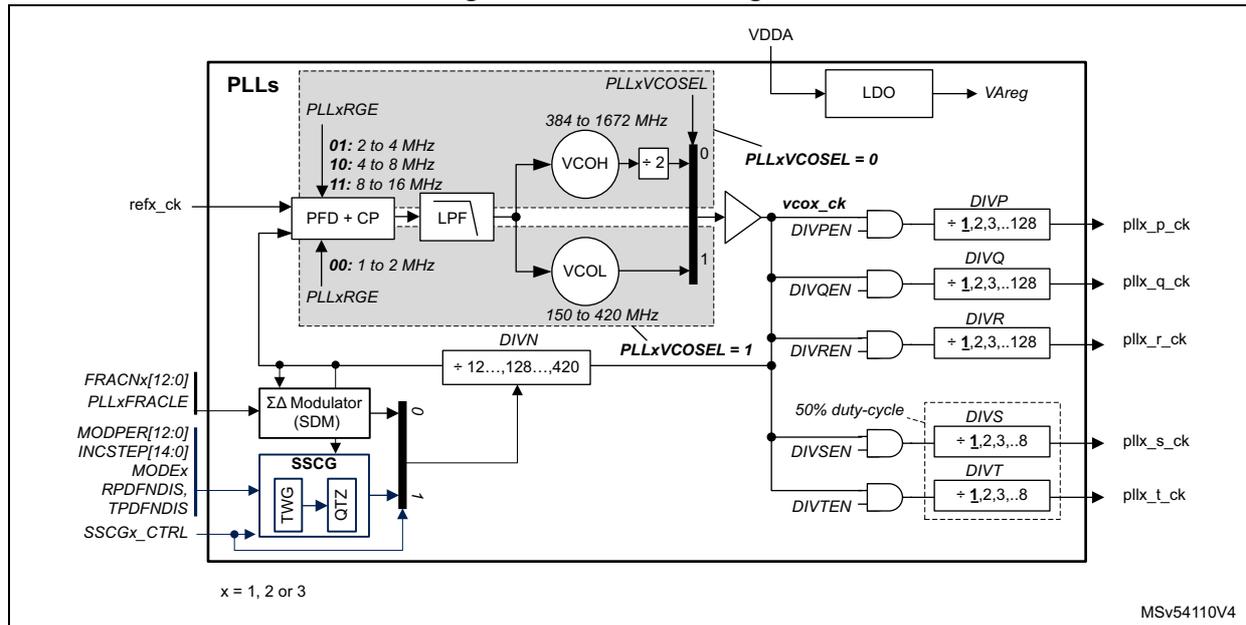
x = 1, 2 or 3 MSv54110V4
The PLLs can be enabled by setting PLLxON to 1. The PLLxRDY bits indicate that the PLL is ready (means locked).
The DIVN loop divider must be programmed to achieve the expected frequency at VCO output. The VCO output range must be respected.
PLLs have a divider-by-2, at VCOH output, insuring that the clock provided to the post-dividers has a duty-cycle of 50%.
The frequency of the clocks provided by the PLLs can also be adjusted thanks to post-divider DIVP , DIVQ , DIVR , DIVS and DIVT . The post-divider values can be changed without disabling the PLLs, if their respective enable bits are set to 0.
The post-dividers provide clocks with 50% duty-cycle in the following conditions:
- • When the post-dividers are dividing the clock by an even value.
- • When VCOH is used and post-dividers are bypassed.
- • When VCOH is selected and post-dividers DIVS and DIVT are used,
PLL programming recommendations
This section is providing a list of recommendations to follow in order to guarantee a good usage of the PLLs. Note that programming examples are given in Section 1.6.2: PLL programming.
- • Before enabling the PLLs, the user must ensure that the reference frequency ( refx_ck ) provided to the PLL is stable and in the good range.
- • When one or several PLL outputs are not used, the application must set the corresponding enable bit DIV[y]ENx and the divider value DIV[y]x to 0 (with x = 1, 2 or 3, and y = P, Q, R, S or T).
- • In order to ensure the good behavior of the PLL, the bits PLLxPEN , PLLxQEN , PLLxREN , PLLxSEN and PLLxTEN must be set to 0 before disabling the corresponding PLL. In the same way, the bits PLLxPEN , PLLxQEN , PLLxREN ,
PLLxSEN and PLLxTEN can be set to 1 only if the corresponding bit PLLON is already set to 1 and the PLL is ready.
Refer to section Section 7.7.1: PLL programming procedure for additional information.
PLL protections
- • The RCC hardware does not allow changing DIVMx, DIVN, PLLxRGE, PLLxVCOSEL when the corresponding PLLx is ON and it is also not possible to change PLLSRC when one of the PLL is ON.
- • The RCC hardware does not allow changing of the post-dividers' DIVy when the corresponding PLLxyEN bit is set to 1 (with x = 1, 2 or 3, and y = P, Q, R, S or T).
- • The hardware prevents writing PLL1ON or PLL1PEN to 0 if the PLL1 is currently used to deliver the system clock. There are other hardware protections on the clock generators (refer to Section 7.5.7: Clock protection ).
The PLLs are disabled by hardware when the system enters Stop or Standby mode
PLLs using HSE as reference clock are also disabled by hardware if an HSE failure is detected.
Note: The
refx_ck
clock is provided to the PLLx when the corresponding PLLON bit is set to 1.
The PLLs can work in 3 different modes:
- • In integer mode
- • In fractional mode
- • In spread spectrum mode
Using the PLLs in integer mode
The PLL is working in integer mode when the sigma-delta modulator (SDM) is loaded with a 0, and the bit PLLxSSCGEN = 0.
In order to load 0 into the SDM, the user has to perform the following sequence:
- – Write PLLxFRACLE of RCC PLLs configuration register (RCC_PLLCFGR) to 0
- – Write FRACN[12:0] to 0,
- – Write PLLxFRACLE to 1
- – Wait at least 5 µs
The bits FRACN[12:0] are located in the RCC_PLLxFRACR registers.
The VCO frequency ( \( F_{VCO} \) ) and output frequencies expressions are given by the following table:
Table 60. VCO frequency and output frequency in integer mode
| PLLxVCOSEL = 0 | PLLxVCOSEL = 1 |
|---|---|
| \( F_{VCO} = 2 \times F_{ref\_ck} \times (DIVN + 1) \) | \( F_{VCO} = F_{ref\_ck} \times (DIVN + 1) \) |
\[
F_{pll\_y\_ck} = \frac{F_{VCO}}{2 \times (DIVy + 1)}
\] with y = P, Q, R, S or T | \[
F_{pll\_y\_ck} = \frac{F_{VCO}}{(DIVy + 1)}
\] with y = P, Q, R, S or T |
Refer to section Section 7.7.1: PLL programming procedure for additional information.
Using the PLLs in fractional mode
The fractional mode is activated when the value loaded into the SDM is different from 0, and the bit PLLxSSCGEN = 0.
The SDM value can be updated at anytime by the application by executing the following sequence:
- – Write PLLxFRACLE bit to '0'
- – Write into FRACN[12:0] the new fractional value,
- – Write PLLxFRACLE to '1'.
The new FRACN value is loaded into the SDM when PLLxFRACLE bit goes from 0 to 1. - – Wait at least 5 µs
The sigma delta modulator is designed in order to minimize the jitter impact while allowing very small frequency steps.
When the PLL is used in fractional mode, the DIVN divider must be initialized before enabling the PLL.
This feature can be used either to generate a specific frequency, with a good accuracy from any crystal value, or to perform a fine tuning of the frequency on-the-fly.
The VCO frequency ( \( F_{VCO} \) ) and output frequencies expressions are given by the following table:
Table 61. VCO frequency and output frequency in fractional mode
| PLLxVCOSEL = 0 | PLLxVCOSEL = 1 |
|---|---|
\[
F_{VCO} = 2 \times F_{ref\_ck} \times \left( DIVN + 1 + \frac{FRACN}{2^{13}} \right)
\] | \[
F_{VCO} = F_{ref\_ck} \times \left( DIVN + 1 + \frac{FRACN}{2^{13}} \right)
\] |
\[
F_{pll\_y\_ck} = \frac{F_{VCO}}{2 \times (DIVy + 1)}
\] with y = P, Q, R, S or T | \[
F_{pll\_y\_ck} = \frac{F_{VCO}}{(DIVy + 1)}
\] with y = P, Q, R, S or T |
Refer to section Section 7.7.1: PLL programming procedure for additional information.
Using the PLLs in spread spectrum mode
The spread spectrum mode is activated when the SDM loaded with 0, and the bit PLLxSSCGEN = 1. This feature is available on all PLLs.
The VCOH must be selected when the spread spectrum mode is activated. VCOH is selected by setting PLLxVCOSEL to 0. PLLxVCOSEL are located into the RCC clock configuration register (RCC_CFGR) .
The spread spectrum technique consist of modulating the VCO frequency with a low-frequency signal (in our case a triangular signal), in order to spread the clock energy into a wider frequency band. As a consequence, the amount of emitted EMI peaks is reduced.
The parameters of the spread spectrum modulation are adjusted via the following fields:
- • MODPER[12:0]: used to adjust the modulation frequency
- • INCSTEP[14:0]: used to adjust the modulation depth (or modulation index)
- • SPREADSEL: used to define if the modulation is centered around the VCO frequency (center-spread) or if it is lowered with respect to VCO frequency (down-spread).
The bits MODPER[12:0], INCSTEP[14:0] and SPREADSEL are located into the RCC_PLLxSSCGR registers with x=1, 2 or 3.
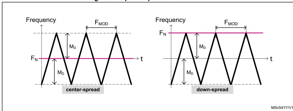
Figure 49 shows the signal modulating the nominal frequency ( \( F_N \) ), when SPREADSEL = 0 (center-spread) and SPREADSEL = 1 (down-spread). The nominal frequency is the frequency output by the PLL in integer mode, when no clock spreading is applied.
Setting the SPREADSEL bit to '1' (down-spread) guarantees that the PLL output frequency does not exceed the programmed frequency value when the SSCG is enabled.
Figure 49. Spread-spectrum modulation
MSV54111V1
The peak modulation depth (in percentage) is given by the following formula:
Note that MODPER x INCSTEP must not exceed \( (2^{15}-1) \) .
The modulation frequency ( \( F_{\text{mod}} \) ) is given by:
Note: Refer to the datasheet of the product for the recommended modulation frequency range
In order to use the spread spectrum feature, the user has to do the following:
- • Program the PLL as explained into Section : Using the PLLs in integer mode in order to adjust the nominal frequency ( \( F_N \) ) according to the targeted by the application.
- • Compute the MODPER value according to the wanted modulation frequency ( \( F_{\text{mod}} \) ):
- • Compute the INCSTEP value according to the wanted modulation depth ( \( M_D \) ):
Check that MODPER x INCSTEP does not exceed \( (2^{15}-1) \) .
- • Then DIVP, Q, R, S or T can be adjusted, and the bit PLLxSSCGEN can be set to 1, and the PLL enabled.
The user can check \( F_{MIN} \) , \( F_{MAX} \) and \( F_C \) as follow:
- • If SSCG_MODE = '0' (centered-spread)
\( F_C \) is given by the formula of the Section : Using the PLLs in integer mode
\( F_{MIN} = F_C \times (1 - M_D/100) \)
\( F_{MAX} = F_C \times (1 + M_D/100) \) - • If SSCG_MODE = '1' (down-spread)
\( F_{MAX} \) is given by the formula of the Section : Using the PLLs in integer mode
\( F_{MIN} = F_{MAX} \times (1 - 2 \times M_D/100) \)
\( F_C = F_{MAX} \times (1 - M_D/100) \)
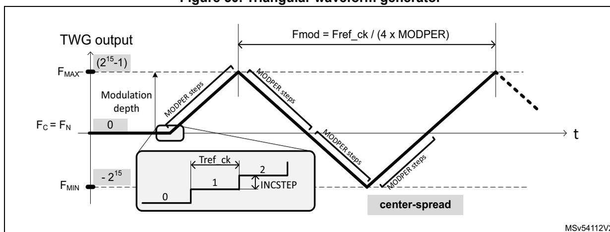
Figure 50 shows the digital signal generated by Triangular Waveform Generator (TWG block), and the way of MODPER and INCSTEP are changing the triangular waveform.
Figure 50. Triangular waveform generator
Refer to section Section 7.7.1: PLL programming procedure for additional information.
7.5.6 System clock (sys_ck)
System clock selection
After a system reset, the HSI is selected as system clock and all PLLs are switched OFF. When a clock source is used for the system clock, it is not possible for the software to disable the selected source via the xxxON bits.
Of course, the system clock can be stopped by the hardware when the system enters Stop or Standby mode.
When the system is running, the user application can select the system clock ( sys_ck ) among the 4 following sources:
- • HSE
- • HSI
- • CSI
- • pll1_p_ck
This function is controlled by programming the RCC clock configuration register (RCC_CFGR) . A switch from one clock source to another occurs only if the target clock
source is ready (clock stable after startup delay or PLL locked). If a clock source that is not yet ready is selected, the switch occurs when the clock source is ready.
The SWS status bits in the RCC clock configuration register (RCC_CFGR) indicate which clock is currently used as system clock. The other status bits in the RCC_CR register indicate which clock(s) is (are) ready.
System clock generation
Figure 51 shows a simplified view of the clock distribution for the CPU and busses. All the dividers shown in the block diagram can be changed on-the-fly without generating timing violations. This feature is a very simple solution to adapt the busses frequencies to the application needs, thus optimizing the power consumption.
The CPRE divider can be used to adjust the CPU clock. However this also impacts the clock frequency of all bus matrix. CPRE is controlled via RCC_CDCFGR register.
In the same way, BMPRE divider can be used to adjust the clock for the bus matrix (AHB and AXI), but this also impacts the clock frequency of APB busses. BMPRE is controlled via RCC_BMCFGR register.
Most of the prescalers are controlled via RCC_CDCFGR and RCC_SRDCFGR registers.
Figure 51. Core and bus clock generation
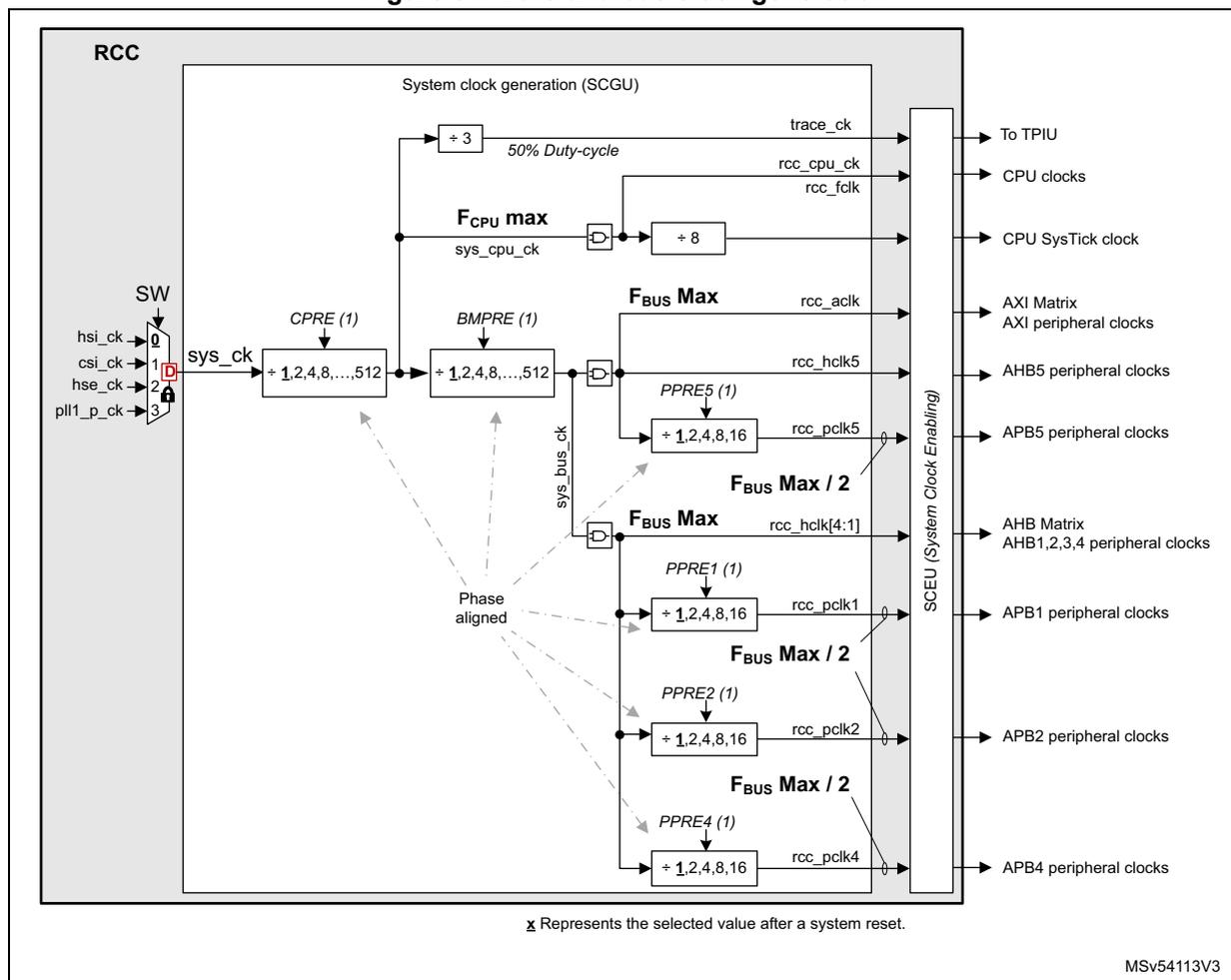
The diagram illustrates the clock generation and distribution within the RCC (Reset and Clock Control) block. On the left, the system clock ( sys_ck ) is selected from four sources via a multiplexer (SW): hsi_ck (0), csi_ck (1), hse_ck (2), and pll1_p_ck (3). The sys_ck signal is distributed to several components:
- A ÷ 3 divider generates the trace_ck clock (50% Duty-cycle) for the TPIU.
- A divider labeled FCPU max generates the sys_cpu_ck clock. This clock is further divided by ÷ 8 to produce rcc_folk (CPU SysTick clock) and rcc_cpu_ck (CPU clocks).
- A divider labeled CPRE (1) with options + 1,2,4,8,...,512 generates the sys_bus_ck clock.
- A divider labeled BMPRE (1) with options + 1,2,4,8,...,512 also generates the sys_bus_ck clock.
The sys_bus_ck clock is distributed to various peripheral clock generators:
- A divider labeled FBUS Max generates rcc_aclk (AXI Matrix AXI peripheral clocks).
- A divider labeled PPRE5 (1) with options + 1,2,4,8,16 generates rcc_hclk5 (AHB5 peripheral clocks).
- A divider labeled FBUS Max / 2 generates rcc_hclk[4:1] (AHB Matrix AHB1,2,3,4 peripheral clocks).
- Four dividers labeled PPRE1 (1) , PPRE2 (1) , PPRE3 (1) , and PPRE4 (1) with options + 1,2,4,8,16 generate rcc_pclk1 (APB1 peripheral clocks), rcc_pclk2 (APB2 peripheral clocks), rcc_pclk3 (APB3 peripheral clocks), and rcc_pclk4 (APB4 peripheral clocks) respectively.
All dividers are Phase aligned to the sys_ck clock. A vertical block labeled SCEU (System Clock Enabling) controls the output of the various clock signals. A note at the bottom indicates that x represents the selected value after a system reset. The document code MSV54113V3 is shown in the bottom right corner.
1. Dividers values can be changed on-the-fly. All dividers provide have 50% duty-cycles.
Note that the application must respect the maximum allowed frequencies: F CPU Max and F BUS Max . F BUS represents the maximum allowed frequency for the AHB and AXI busses. Refer to the product datasheet for maximum values.
Note as well that the trace clock ( trace_ck ) is generated from sys_cpu_ck clock, divided by 3. For additional information refer to Section : Clock distribution for Debug and Trace .
7.5.7 Clock protection
The RCC does not allow to disable the system clock ( sys_ck ). Several protections are implemented in order to prevent actions disabling accidentally the system clock.
In addition, protection bits are available in order to prevent accidental disabling of FMC and XSPI block activities.
The protections consist on ignoring the invalid write operations. It is recommended to read back registers having protection to insure that the clock configuration expected by the software is accepted by the RCC.
The table hereafter shows the protections handled by the RCC.
Table 62. Clock protection summary
| Protected fields | Conditions checked by the RCC |
|---|---|
| SW[2:0] | Changing SW value is allowed only if the targetted clock is enabled and ready. |
| PLLSRC[1:0] | Changing PLLSRC value is allowed if: - The targetted clock is enabled and ready, and, - All PLL disabled |
| HSEON, HSION or CSION | Changing these fields is allowed if: - The oscillator is not used directly or indirectly (via PLL1) as system clock, and - FMCCKP = XSPICKP = 0. |
| DIVMx[5:0], PLLxRGE[1:0], PLLxVCOSEL, DIVN[8:0] | Changing these fields is allowed only if the corresponding PLL is disabled (PLLxON=0) |
| DIVP[6:0], DIVQ[6:0], DIVR[6:0], DIVS[2:0], DIVT[2:0] | Changing these fields is allowed only if the corresponding DIVyEN bit is equal to 0 (y = P, Q, R, S or T) |
| PLL1ON | Changing this field is allowed if: - SW switch is not selecting the PLL1, and - FMCCKP = 0. |
| PLL1PEN | Disabling the DIVP output of PLL1 is allowed if the SW switch is not selecting PLL1 |
| PLL2ON | Changing this field is allowed only if FMCCKP = XSPICKP = 0. |
| PLL2SEN, PLL2TEN, XSPI1EN XSPI2EN, XSPI1LPEN XSPI2LPEN, XSPI1RST XSPI2RST | Changing these fields is allowed only if XSPICKP = 0. |
| PLL1QEN, PLL2REN, FMCEN, FMCLPEN, FMCRST | Changing these fields is allowed only if FMCCKP = 0. |
| HSEBYP, HSEEXT | Changing these fields is allowed only if HSEON = 0. |
| LSEBYP, LSEEXT | Changing these fields is allowed only if LSEON = 0. |
There is also clock protection mechanism in case of HSE failure, refer to Section : CSS on HSE .
7.5.8 Clock generation in Stop and Standby modes
When the whole system enters Stop mode, all the clocks (system and kernel clocks) are stopped and the following clock sources are disabled as well:
- • CSI, HSI (depending on HSIKERON, and CSIKERON bits)
- • HSE
- • PLL1, PLL2 and PLL3
- • HSI48
The content of the RCC registers is not altered except for PLL1ON, PLL2ON, PLL3ON, HSEON and HSI48ON that are set to 0.
HSION and CSION bits are also affected depending on STOPWUCK and STOPKERWUCK bits (see Table 63 ).
When the CPU requested to go in Stop mode, the RCC first stop all the requested clocks, and inform the PWR that all clocks have been properly stopped. As shown in Figure 52 , three main signals are used to control power transitions:
- • The rcc_pwrds is used to indicate to the PWR that the RCC has stopped all the clocks, and thus the PWR can go to Stop or Standby.
- • The pwr_wkup is used to indicate to the RCC to re-enable the clocks.
- • The exti_wkup is used to indicate to the PWR that an event requests to exit the system from Stop mode.
Figure 52. Key signals controlling low-power modes
graph LR
    WE[Wake-up events] --> EXTI[EXTI]
    EXTI -- exti_wkup --> PWR[PWR]
    PWR -- pwr_wkup --> RCC[RCC]
    RCC -- rcc_pwrds --> PWR
    SYSCK((sys_ck)) --> PWR
    SYSCK --> RCC
Exiting Stop mode
When the microcontroller exits system Stop mode via a wake-up event, the application can select which oscillator (HSI and/or CSI) is used to restart. The STOPWUCK bit selects the oscillator used as system clock. The STOPKERWUCK bit selects the oscillator used as kernel clock for peripherals. The STOPKERWUCK bit is useful if after a system Stop, a peripheral needs a kernel clock generated by an oscillator different from the one used for the system clock.
All these bits belong to the RCC clock configuration register (RCC_CFGR) .
Table 63 gives a detailed description of their behavior.
Table 63. STOPWUCK and STOPKERWUCK description
| STOPWUCK | STOPKERWUCK | - | Activated oscillator when system exits Stop mode | Distributed clocks when system exits Stop mode | |
|---|---|---|---|---|---|
| System clock | Kernel clock | ||||
| 0 | 0 | → | HSI | HSI | HSI |
| 1 | → | HSI and CSI | HSI and/or CSI | ||
| 1 | 0 | → | CSI | CSI | CSI |
| 1 | → | ||||
During Stop mode
There are two specific cases where the HSI or CSI can be enabled during system Stop mode:
- • when a dedicated peripheral requests the kernel clock
The peripheral receives the HSI or CSI according to the kernel clock source selected for this peripheral (via PERxSRC). - • when the HSIKERON or CSIKERON bits are set the HSI and CSI are kept running during Stop mode but the outputs are gated. The clock is then available immediately when the system exits Stop mode or when a peripheral requests the kernel clock (see Table 64 for details).
HSIKERON and CSIKERON bits belong to RCC register map . Table 64 gives a detailed description of their behavior.
Table 64. HSIKERON and CSIKERON behavior
| HSIKERON (CSIKERON) | - | HSI (CSI) state during Stop mode | HSI (CSI) setting time |
|---|---|---|---|
| 0 | → | OFF | \( t_{su(HSI)} \) ( \( t_{su(CSI)} \) ) (1) |
| 1 | → | Running and gated | Immediate |
- 1. \( t_{su(HSI)} \) and \( t_{su(CSI)} \) are the startup times of the HSI and CSI oscillators (refer to the product datasheet for values of these parameters).
When the microcontroller exists Standby mode, the HSI is selected as system and kernel clock. The RCC registers are reset to their initial values except for the RCC_RSR and RCC_BDCR registers.
Note that the HSI and CSI outputs provide two clock paths (see Figure 40 ):
- • one path for the system clock ( hsi_ck or csi_ck )
- • one path for the peripheral kernel clock ( hsi_ker_ck or csi_ker_ck ).
When a peripheral requests the kernel clock in system Stop mode, only the path providing the hsi_ker_ck or csi_ker_ck is activated.
Caution: The CPU does not get automatically the same clock frequencies when leaving Stop mode: it is up to the application to restore the previous clock settings if needed.
7.5.9 Peripheral clock distribution
Some peripherals are designed to work with two different clock domains that operate asynchronously:
- • a clock domain synchronous with the register and bus interface ( ckg_bus_perx clock)
- • a clock domain generally synchronous with the peripheral (kernel clock)
The benefit of having peripherals supporting these two clock domains is that the user application has more freedom to choose optimized clock frequency for the CPU, bus matrix and for the kernel part of the peripheral.
As a consequence, the user application can change the bus frequency without reprogramming the peripherals. As an example an on-going transfer with UART is not disturbed if its APB clock is changed on-the-fly.
Table 65 shows the clocks the RCC delivers to the peripherals. Note as well that the clock named per_ck, is the output of a mux which allows the application to select:
- • hsi_ker_ck, or
- • csi_ker_ck, or
- • hse_ker_ck
Table 65. Peripheral clock distribution summary
| Peripherals | Clock types | Clock sources | Kernel clock MUX | Max Kernel clock freq. [MHz] (1) | Type (2)(3) | |
|---|---|---|---|---|---|---|
| Pos. | Control field | |||||
| ADF | Kernel | hclk1 | 0 (4) | ADF1SEL | F MAX / 2 | A |
| pll2_p_ck | 1 | |||||
| pll3_p_ck | 2 | |||||
| i2s_ckin | 3 | |||||
| csi_ker_ck | 4 | |||||
| hsi_ker_ck | 5 | |||||
| Bus | hclk1 | - | - | F MAX / 2 | - | |
| ADC12 | Kernel | pll2_p_ck | 0 (4) | ADCSEL | 125 | A |
| pll3_r_ck | 1 | |||||
| per_ck | 2 | |||||
| Bus | hclk1 | - | - | F MAX / 2 | - | |
| CORDIC | Bus | hclk2 | - | - | F MAX / 2 | - |
| CRC | Bus | hclk4 | - | - | F MAX / 2 | - |
| CRS | Bus | pclk1 | - | - | F MAX / 4 | - |
| CRYP | Bus | hclk3 | - | - | F MAX / 2 | - |
| DBG | Bus | sys_bus_ck | - | - | F MAX / 2 | - |
| kernel | sys_cpu_ck/3 | - | - | F MAX / 3 | - | |
| DB_OCSPI1. DB_OCSPI2 | Bus | hclk5 | - | - | F MAX / 2 | - |
Table 65. Peripheral clock distribution summary
| Peripherals | Clock types | Clock sources | Kernel clock MUX | Max Kernel clock freq. [MHz] (1) | Type (2)(3) | |
|---|---|---|---|---|---|---|
| Pos. | Control field | |||||
| DB_SDMMC1 | Bus | hclk5 | - | - | F MAX / 2 | - |
| DB_SDMMC2 | Bus | hclk2 | - | - | F MAX / 2 | - |
| DCMIPP | Bus | aclk | - | - | F MAX / 2 | - |
| pclk5 | F MAX / 4 | |||||
| GPDMA1 | Bus | hclk1 | - | - | F MAX / 2 | - |
| HPDMA1 | Bus | hclk5 | - | - | F MAX / 2 | - |
| aclk | ||||||
| DMA2D | Bus | hclk5 | - | - | F MAX / 2 | - |
| aclk | ||||||
| ETH1 | Kernel | ETH_MII_TX_CLK | - | - | 25 | A |
| ETH_MII_TX_CLK/ ETH_RMII_REF_CLK | 0 (4) | ETH1REFCKSEL | 25 | A | ||
| hse_ker_ck | 1 | |||||
| eth_clk_fb | 2 | |||||
| hse_ker_ck | 0 (4) | ETH1PHYCKSEL | 50 | A | ||
| pll3_s_ck | 1 | |||||
| clk_ptp_ref_i | F MAX / 2 | - | ||||
| Bus | hclk1 | - | - | F MAX / 2 | - | |
| EXTI | Bus | pclk4 | - | - | F MAX / 4 | - |
| FLASH | Bus | hclk5 | - | - | F MAX / 2 | - |
| FDCAN | Kernel | hse_ker_ck | 0 (4) | FDCANSEL | 125 | A |
| pll1_q_ck | 1 | |||||
| pll2_p_ck | 2 | |||||
| Bus | pclk1 | - | - | F MAX / 4 | - | |
| FMC | Kernel | hclk5 | 0 (4) | FMCSEL | F MAX / 2 | A |
| pll1_q_ck | 1 | |||||
| pll2_r_ck | 2 | |||||
| hsi_ker_ck | 3 | |||||
| Bus | hclk5 | - | - | F MAX / 2 | - | |
| aclk | ||||||
| GPIOA-H, GPIOM-P | Bus | hclk4 | - | - | F MAX / 2 | - |
| GPU2D | Bus | hclk5 | - | - | F MAX / 2 | - |
| aclk | ||||||
Table 65. Peripheral clock distribution summary
| Peripherals | Clock types | Clock sources | Kernel clock MUX | Max Kernel clock freq. [MHz] (1) | Type (2)(3) | |
|---|---|---|---|---|---|---|
| Pos. | Control field | |||||
| GFXMMU | Bus | hclk5 | - | - | F MAX / 2 | - |
| aclk | ||||||
| GFXTIM | Bus | pclk5 | - | - | F MAX / 4 | - |
| HASH | Bus | hclk3 | - | - | F MAX / 2 | - |
| HDMI-CEC | Kernel | lse_ck | 0 (4) | CECSEL | 1 | - |
| lsi_ck | 1 | |||||
| csi_ker_ck/122 | 2 | |||||
| Bus | pclk1 | - | - | F MAX / 4 | ||
| I2C2, I2C3 | Kernel | pclk1 | 0 (4) | I2C23SEL | F MAX / 4 | A |
| pll3_r_ck | 1 | |||||
| hsi_ker_ck | 2 | |||||
| csi_ker_ck | 3 | |||||
| Bus | pclk1 | - | - | F MAX / 4 | - | |
| I2C1/I3C1 | Kernel | pclk1 | 0 (4) | I2C1_I3C1SEL | F MAX / 4 | A |
| pll3_r_ck | 1 | |||||
| hsi_ker_ck | 2 | |||||
| csi_ker_ck | 3 | |||||
| Bus | pclk1 | - | - | F MAX / 4 | - | |
| XSPIM | Bus | hclk5 | - | - | F MAX / 2 | - |
| IWDG | Kernel | lsi_ck | - | - | 1 | A |
| Bus | pclk4 | - | - | F MAX / 4 | - | |
| JPEG | Bus | hclk5 | - | - | F MAX / 2 | - |
| LPTIM1 | Kernel | pclk1 | 0 (4) | LPTIM1SEL | F MAX / 4 | A |
| pll2_p_ck | 1 | |||||
| pll3_r_ck | 2 | |||||
| lse_ck | 3 | |||||
| lsi_ck | 4 | |||||
| per_ck | 5 | |||||
| Bus | pclk1 | - | - | F MAX / 4 | - | |
Table 65. Peripheral clock distribution summary
| Peripherals | Clock types | Clock sources | Kernel clock MUX | Max Kernel clock freq. [MHz] (1) | Type (2)(3) | |
|---|---|---|---|---|---|---|
| Pos. | Control field | |||||
| LPTIM2, LPTIM3 | Kernel | pclk4 | 0 (4) | LPTIM23SEL | F MAX / 4 | A |
| pll2_p_ck | 1 | |||||
| pll3_r_ck | 2 | |||||
| lse_ck | 3 | |||||
| lsi_ck | 4 | |||||
| per_ck | 5 | |||||
| Bus | pclk4 | - | - | F MAX / 4 | - | |
| LPTIM4, LPTIM5 | Kernel | pclk4 | 0 (4) | LPTIM45SEL | F MAX / 4 | A |
| pll2_p_ck | 1 | |||||
| pll3_r_ck | 2 | |||||
| lse_ck | 3 | |||||
| lsi_ck | 4 | |||||
| per_ck | 5 | |||||
| Bus | pclk4 | - | - | F MAX / 4 | - | |
| LPUART1 | Kernel | pclk4 | 0 (4) | LPUART1SEL | F MAX / 4 | A |
| pll2_q_ck | 1 | |||||
| pll3_q_ck | 2 | |||||
| hsi_ker_ck | 3 | |||||
| csi_ker_ck | 4 | |||||
| lse_ck | 5 | |||||
| Bus | pclk4 | - | - | F MAX / 4 | - | |
| LTDC | Kernel | pll3_r_ck | - | - | 90 | A |
| Bus | pclk5 | - | F MAX / 4 | - | ||
| aclk | - | F MAX / 2 | ||||
| MCE1, MCE2, MCE3 | Bus | aclk | - | - | F MAX / 2 | - |
| hclk5 | - | |||||
| MDIO | Bus | pclk1 | - | - | F MAX / 4 | - |
| PKA | Bus | hclk3 | - | - | F MAX / 2 | - |
| PWR | Bus | hclk4 | - | - | F MAX / 2 | - |
| PSSI | Kernel | pll3_r_ck | 0 (4) | PSSISEL | 100 | - |
| per_ck | 1 | - | ||||
| Bus | hclk2 | - | - | F MAX / 2 | - | |
Table 65. Peripheral clock distribution summary
| Peripherals | Clock types | Clock sources | Kernel clock MUX | Max Kernel clock freq. [MHz] (1) | Type (2)(3) | |
|---|---|---|---|---|---|---|
| Pos. | Control field | |||||
| XSPI1 | Kernel | hclk5 | 0 (4) | XSPI1SEL | F MAX / 2 | A |
| pll2_s_ck | 1 | |||||
| pll2_t_ck | 2 | |||||
| Bus | hclk5 | - | - | F MAX / 2 | - | |
| aclk | ||||||
| XSPI2 | Kernel | hclk5 | 0 (4) | XSPI2SEL | F MAX / 2 | A |
| pll2_s_ck | 1 | |||||
| pll2_t_ck | 2 | |||||
| Bus | hclk5 | - | - | F MAX / 2 | - | |
| aclk | ||||||
| OTGFS | Kernel | hsi48_ker_ck | 0 (4) | OTGFSSEL | 50 | A |
| pll3_q_ck | 1 | |||||
| hse_ker_ck | 2 | |||||
| clk48mohci | 3 | |||||
| Bus | hclk1 | - | - | F MAX / 2 | - | |
| OTGHS | Kernel | phy60m_ck | - | - | 60 | A |
| Bus | hclk1 | - | - | F MAX / 2 | - | |
| RCC | Bus | hclk4 | - | - | F MAX / 2 | - |
| RNG | Kernel | hsi48_ker_ck | - | - | 48 | A |
| Bus | hclk3 | - | - | F MAX / 2 | - | |
| RTC/AWU (5) | Kernel | no clock | 0 (4) | RTCSEL | 4 | A |
| lse_ck | 1 | |||||
| lsi_ck | 2 | |||||
| hse_ker_ck / (RTCDIV+1) | 3 | |||||
| Bus | pclk4 | - | - | F MAX / 4 | - | |
| SAES | Kernel | hclk3 | - | - | F MAX / 2 | A |
| Bus | hclk3 | - | - | F MAX / 2 | - | |
| SAI1 | Kernel | pll1_q_ck | 0 (4) | SAI1SEL | 133 | A |
| pll2_p_ck | 1 | |||||
| pll3_p_ck | 2 | |||||
| I2S_CKIN | 3 | |||||
| per_ck | 4 | |||||
| Bus | pclk2 | - | - | F MAX / 4 | - | |
Table 65. Peripheral clock distribution summary
| Peripherals | Clock types | Clock sources | Kernel clock MUX | Max Kernel clock freq. [MHz] (1) | Type (2)(3) | |
|---|---|---|---|---|---|---|
| Pos. | Control field | |||||
| SAI2 | Kernel | pll1_q_ck | 0 (4) | SAI2SEL | 133 | A |
| pll2_p_ck | 1 | |||||
| pll3_p_ck | 2 | |||||
| i2s_ckin | 3 | |||||
| per_ck | 4 | |||||
| spdif_symb_ck | 5 | |||||
| Bus | pclk2 | - | - | F MAX / 4 | - | |
| SBS | Bus | pclk4 | - | - | F MAX / 4 | - |
| SDMMC1 | Kernel | pll2_s_ck | 0 (4) | SDMMC12SEL | 200 | A |
| pll2_t_ck | 1 | |||||
| Bus | hclk5 | - | - | F MAX / 2 | - | |
| SDMMC2 | Kernel | pll2_s_ck | 0 (4) | SDMMC12SEL | 200 | A |
| pll2_t_ck | 1 | |||||
| Bus | hclk2 | - | - | F MAX / 2 | - | |
| SPDIFRX | Kernel | pll1_q_ck | 0 (4) | SPDIFRXSEL | 200 | A |
| pll2_r_ck | 1 | |||||
| pll3_r_ck | 2 | |||||
| hsi_ker_ck | 3 | |||||
| Bus | pclk1 | - | - | F MAX / 4 | - | |
| SPI/I2S6 | Kernel | pclk4 | 0 (4) | SPI6SEL | 200 | A |
| pll2_q_ck | 1 | |||||
| pll3_q_ck | 2 | |||||
| hsi_ker_ck | 3 | |||||
| csi_ker_ck | 4 | |||||
| hse_ker_ck | 5 | |||||
| Bus | pclk4 | - | - | F MAX / 4 | - | |
| SPI/I2S1 | Kernel | pll1_q_ck | 0 (4) | SPI1SEL | 130 | A |
| pll2_p_ck | 1 | |||||
| pll3_p_ck | 2 | |||||
| i2s_ckin | 3 | |||||
| per_ck | 4 | |||||
| Bus | pclk2 | - | - | F MAX / 4 | - | |
Table 65. Peripheral clock distribution summary
| Peripherals | Clock types | Clock sources | Kernel clock MUX | Max Kernel clock freq. [MHz] (1) | Type (2)(3) | |
|---|---|---|---|---|---|---|
| Pos. | Control field | |||||
| SPI4, SPI5 | Kernel | pclk2 | 0 (4) | SPI45SEL | 200 | A |
| pll2_q_ck | 1 | |||||
| pll3_q_ck | 2 | |||||
| hsi_ker_ck | 3 | |||||
| csi_ker_ck | 4 | |||||
| hse_ker_ck | 5 | |||||
| Bus | pclk2 | - | - | F MAX / 4 | - | |
| SPI/I2S3, SPI/I2S2 | Kernel | pll1_q_ck | 0 (4) | SPI23SEL | 200 | A |
| pll2_p_ck | 1 | |||||
| pll3_p_ck | 2 | |||||
| I2S_CKIN | 3 | |||||
| per_ck | 4 | |||||
| Bus | pclk1 | - | - | F MAX / 4 | - | |
| TAMPER | Kernel | no clock | 0 (4) | RTCSEL | 4 | A |
| lse_ck | 1 | |||||
| lsi_ck | 2 | |||||
| hse_ker_ck/ (RTCDIV+1) | 3 | |||||
| Bus | pclk4 | - | - | F MAX / 4 | - | |
| DTS | Kernel | lse_ck | - | - | 10 | A |
| Bus | pclk4 | - | - | F MAX / 4 | - | |
| TIM2, TIM3, TIM4, TIM5, TIM6, TIM7, TIM12, TIM13, TIM14 | Kernel | timg1_ck | - | - | F MAX / 2 | S |
| Bus | pclk1 | - | - | F MAX / 4 | - | |
| TIM1, TIM9, TIM15, TIM16, TIM17, | Kernel | timg2_ck | - | - | F MAX / 2 | S |
| Bus | pclk2 | - | - | F MAX / 4 | - | |
| USART1, | Kernel | pclk2 | 0 (4) | USART1SEL | F MAX / 4 | A |
| pll2_q_ck | 1 | |||||
| pll3_q_ck | 2 | |||||
| hsi_ker_ck | 3 | |||||
| csi_ker_ck | 4 | |||||
| lse_ck | 5 | |||||
| Bus | pclk2 | - | - | F MAX / 4 | - | |
Table 65. Peripheral clock distribution summary
| Peripherals | Clock types | Clock sources | Kernel clock MUX | Max Kernel clock freq. [MHz] (1) | Type (2)(3) | |
|---|---|---|---|---|---|---|
| Pos. | Control field | |||||
| USART2, USART3, UART4, UART5, UART7, UART8 | Kernel | pclk1 | 0 (4) | UART234578SEL | F MAX / 4 | A |
| pll2_q_ck | 1 | |||||
| pll3_q_ck | 2 | |||||
| hsi_ker_ck | 3 | |||||
| csi_ker_ck | 4 | |||||
| lse_ck | 5 | |||||
| Bus | pclk1 | - | - | F MAX / 4 | - | |
| UCPD | Kernel | ucpd_ker_ck | - | - | 25 | A |
| Bus | pclk1 | - | - | F MAX / 4 | - | |
| USBPHYC | Kernel | hse_ker_ck | 0 (4) | USBPHYCSEL | 32 | A |
| hse_ker_ck / 2 | 1 | |||||
| pll3_q_ck | 2 | |||||
| VREFBUF | Bus | pclk4 | - | - | F MAX / 4 | - |
| WWDG1 | Bus | pclk1 | - | - | F MAX / 4 | - |
1. F MAX value depends on the device reference and can be found on the datasheet of the product.
2. 'A' Means that the kernel clock is asynchronous with respect to bus interface clock.
3. 'S' Means that the kernel clock is synchronous with respect to bus interface clock.
4. Reset value
5. The RTC switch is in the VSW voltage domain
Figure 53 to Figure 68 provide a more detailed description of kernel clock distribution. Refer to Section 7.5.12: Peripheral clock gating control for more details.
To reduce the amount of switches, some peripherals share the same kernel clock source. Nevertheless, all peripherals have their dedicated enable signal.
Clock distribution for ADF, SAIs, and SPDIFRX
The audio peripherals generally need specific accurate frequencies, except for SPDIFRX. As shown in Figure 53 and Figure 56, the kernel clock of the SAIs or SPI(I2S)s can be generated by:
- • PLL1 when the amount of active PLLs must be reduced (for SAIs and SPI/I2S1 to 3)
- • APB2 peripheral clock (for SPI/I2S4 and 5)
- • APB4 peripheral clock (for SPI/I2S6)
- • PLL2 or 3 for optimal flexibility in frequency generation
- • HSE, HSI or CSI for use-cases where the current consumption is critical
- • I2S_CKIN when an external clock reference needs to be used
The SPDIFRX does not require a specific kernel clock frequency but only a frequency high enough to sample properly the incoming stream. Refer to the SPDIFRX description for more details.
The SPDIFRX also provides a symbol clock (spdifrx_symb_ck) which is 64 times faster than the received samples. The symbol clock is proposed as kernel clock for SAI2 in order to ease bridging from SPDIFRX to SAI2.
The audio blocks also have common kernel clocks in order to ease data exchange.
The ADF can work even in Stop mode as long as the bus clock is not requested. Working in Stop mode is possible only if the application selected csi_ker_ck or hsi_ker_ck as kernel clock sources. The ADF asserts the adf_ker_ckreq when the kernel clock is requested.
The kernel clock mechanism works only if the kernel clock source is provided by an RC oscillator ( hsi_ker_ck or csi_ker_ck ).
Figure 53. Clock distribution for SAIs, ADF and SPDIFRX
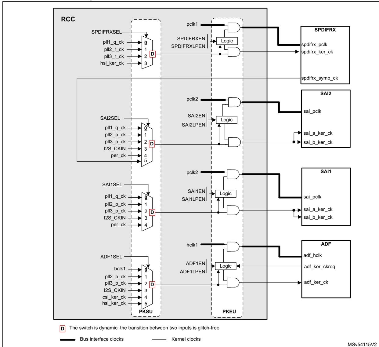
The diagram illustrates the clock distribution for SPDIFRX, SAI2, SAI1, and ADF. The components and their connections are as follows:
- RCC (Reset and Clock Control):
Contains four multiplexers (MUX) for selecting clock sources.
- SPDIFRXSEL: Selects between pll1_q_ck (0), pll2_r_ck (1), pll3_r_ck (2), and hsi_ker_ck (3). The selected clock is labeled pclk1 .
- SAI2SEL: Selects between pll1_q_ck (0), pll2_p_ck (1), pll3_p_ck (2), I2S_CKIN (3), per_ck (4), and hsi_ker_ck (5). The selected clock is labeled pclk2 .
- SAI1SEL: Selects between pll1_q_ck (0), pll2_p_ck (1), pll3_p_ck (2), I2S_CKIN (3), per_ck (4), and hsi_ker_ck (5). The selected clock is labeled pclk2 .
- ADF1SEL: Selects between hclk1 (0), pll2_p_ck (1), pll3_p_ck (2), I2S_CKIN (3), csi_ker_ck (4), and hsi_ker_ck (5). The selected clock is labeled hclk1 .
- PKSU (Peripheral Kernel Switch Unit): Contains four logic blocks (AND gates) that enable the clock signals. Each logic block takes the selected clock from the RCC and a enable signal (SPDIFRXEN, SAI2EN, SAI1EN, or ADF1EN) as input. The output of each logic block is a Kernel clock .
- PKEU (Peripheral Kernel Enable Unit): Contains four logic blocks (OR gates) that generate the enable signals for the peripherals. Each logic block takes the enable signal from the PKSU and a low-power enable signal (SPDIFRXLPEN, SAI2LPEN, SAI1LPEN, or ADF1LPEN) as input.
The peripherals and their clock inputs are:
- SPDIFRX: Receives spdifrx_pclk (bus interface clock), spdifrx_ker_ck (kernel clock), and spdifrx_symb_ck (kernel clock).
- SAI2: Receives sai_pclk (bus interface clock), sai_a_ker_ck (kernel clock), and sai_b_ker_ck (kernel clock).
- SAI1: Receives sai_pclk (bus interface clock), sai_a_ker_ck (kernel clock), and sai_b_ker_ck (kernel clock).
- ADF: Receives adf_hclk (bus interface clock), adf_ker_ckreq (kernel clock), and adf_ker_ck (kernel clock).
Legend:
- D The switch is dynamic: the transition between two inputs is glitch-free.
- Bus interface clocks (thick line)
- Kernel clocks (thin line)
MSV54115V2
- 1. X represents the selected mux input after a system reset.
Clock distribution for SPIs, SPI/I2Ss
SPI peripherals do not need an accurate kernel clock frequency but a clock fast enough for the serial interface. The SPI/I2S peripherals may request accurate kernel clock frequency when using the I2S function. For that purpose the source can be selected among the following ones:
- • The bus clock (for SPIs)
- • PLL1 when the amount of active PLLs must be reduced
- • PLL2 or PLL3 if better flexibility is required. As an example, this solution allows changing the frequency bus via PLL1 without affecting the speed of some serial interfaces.
- • HSI or CSI or per_ck for low-power use-cases.
The SPI/I2S also have common kernel clocks with audio blocks in order to ease data exchange.
Figure 54. Clock distribution for SPIs and SPI/I2S
![Figure 54. Clock distribution for SPIs and SPI/I2S. The diagram shows the internal clock distribution for SPI1/I2S1, SPI1/I2Sy (y=2 or 3), SPI[5:4], and SPI/I2S6. Each SPI/I2S block has a multiplexer (MUX) selecting from various clock sources (PLL1_q_ck, PLL2_p_ck, PLL3_p_ck, I2S_CKIN, per_ck, pclk2, hsi_ker_ck, csi_ker_ck, hse_ker_ck). The selected clock is then passed through a logic block (AND gate) controlled by SPIxEN and SPIxLPEN signals to produce the final spi_pclk and spi_ker_ck outputs. The diagram is divided into RCC, PKSU, and PKEU sections. A legend indicates that 'D' represents a dynamic switch that is glitch-free.](/RM0477-STM32H7Rx-7Sx/8d1d1224d4b047853e460dc17c58383b_img.jpg)
RCC
SPI1SEL
- pll1_q_ck
- pll2_p_ck
- pll3_p_ck
- i2s_ckin
- per_ck
SPI23SEL
- pll1_q_ck
- pll2_p_ck
- pll3_p_ck
- i2s_ckin
- per_ck
SPI45SEL
- pclk2
- pll2_q_ck
- pll3_q_ck
- hsi_ker_ck
- csi_ker_ck
- hse_ker_ck
SPI6SEL
- pclk4
- pll2_q_ck
- pll3_q_ck
- hsi_ker_ck
- csi_ker_ck
- hse_ker_ck
Logic
- pclk2
- SPI1EN
- SPI1LPEN
SPI1/I2S1
- spi_pclk
- spi_ker_ck
Logic
- pclk1
- SPIyEN
- SPIyLPEN
SPI1/I2Sy (y = 2 or 3)
- spi_pclk
- spi_ker_ck
Logic
- pclk2
- SPI[5:4]EN
- SPI[5:4]LPEN
SPI[5:4]
- spi_pclk
- spi_ker_ck
Logic
- pclk4
- SPI6EN
- SPI6LPEN
SPI/I2S6
- spi_pclk
- spi_ker_ck
PKSU PKEU
D The switch is dynamic: the transition between two inputs is glitch-free.
MSV54116V1
- 1. X represents the selected switch input after a system reset.
Clock distribution for I2C[3:2], and I2C1/I3C1
I2Cs and I3C1 peripherals do not need an accurate kernel clock frequency but a clock fast enough to handle properly the serial interface. The following kernel clock sources are proposed:
- • The bus clock
- • PLL3 in the case where the bus clock cannot be used
- • HSI or CSI for low-power use-cases
The I2Cs and I3C1 can work even in Stop mode as long as the bus clock is not requested. Working in Stop mode is possible only if the application selected csi_ker_ck or hsi_ker_ck as kernel clock sources. The I2Cs and I3C1 assert the i2c_ker_ckreq or i3c_ker_ckreq signals, when the kernel clock is requested.
The kernel clock mechanism works only if the kernel clock source is provided by an RC oscillator ( hsi_ker_ck or csi_ker_ck ).
Figure 55. Clock distribution for I2C[3:2] and I2C1/I3C1
![Figure 55: Clock distribution for I2C[3:2] and I2C1/I3C1. The diagram shows the RCC (Reset and Clock Control) block containing two dynamic switches (PKSU) and two logic blocks (PKEU). The top PKSU switch is controlled by I2C1_I3C1SEL and selects between pclk1 (0), pll3_r_ck (1), hsi_ker_ck (2), and csi_ker_ck (3). The bottom PKSU switch is controlled by I2C23SEL and selects between the same four sources. The top PKEU logic block takes pclk1 and I2C1_I3C1EN/I2C1_I3C1LPEN as inputs and outputs i2c/i3c_pclk, i2c/i3c_ker_ckreq, and i2c/i3c_ker_ck to the I2C1/I3C1 block. The bottom PKEU logic block takes pclk1 and I2C[3:2]EN/I2C[3:2]LPEN as inputs and outputs i2c_pclk, i2c_ker_ckreq, and i2c_ker_ck to the I2C2, I2C3 block. A legend indicates that thick lines represent bus interface clocks and thin lines represent kernel clocks. A note states that the switch is dynamic and glitch-free. MSV54117V2.](/RM0477-STM32H7Rx-7Sx/461a7fcfb723298eb0738985adca2c94_img.jpg)
RCC
I2C1_I3C1SEL
pclk1
pll3_r_ck
hsi_ker_ck
csi_ker_ck
0
1
2
3
D
I2C23SEL
pclk1
pll3_r_ck
hsi_ker_ck
csi_ker_ck
0
1
2
3
D
PKSU
pclk1
I2C1_I3C1EN
I2C1_I3C1LPEN
Logic
PKEU
I2C1/I3C1
i2c/i3c_pclk
i2c/i3c_ker_ckreq
i2c/i3c_ker_ck
pclk1
I2C[3:2]EN
I2C[3:2]LPEN
Logic
PKEU
I2C2, I2C3
i2c_pclk
i2c_ker_ckreq
i2c_ker_ck
D The switch is dynamic: the transition between two inputs is glitch-free.
— Bus interface clocks — Kernel clocks
MSV54117V2.
- 1. X represents the selected switch input after a system reset
Clock distribution for UARTs and USARTs
UARTs need kernel clock frequency allowing the adjustment of the baud rate with an acceptable accuracy (generally less than \( \pm 2\% \) ). For that purpose the source can be selected among the following ones:
- • The bus clock
- • PLL3 in the case where the bus clock cannot be used
- • HSI, CSI or LSE for low-power use-cases
The UARTs can work even in Stop mode as long as the bus clock is not requested. Working in Stop mode is possible only if the application selected
csi_ker_ck
or
hsi_ker_ck
as kernel clock sources. The UARTs assert the
uartx_ker_ckreq
signal, when the kernel clock is requested. The kernel clock mechanism works only if the kernel clock source is provided by an RC oscillator (
hsi_ker_ck
or
csi_ker_ck
).
UARTs can also work in Stop mode using the LSE clock when high baud rates are not required.
Figure 56. Clock distribution for UARTs, LPUART1 and USARTs
![Figure 56: Clock distribution for UARTs, LPUART1 and USARTs. The diagram shows the internal clock logic for USART[3:2], UART[y], LPUART1, and USART1. Each peripheral has a 'Logic' block that takes bus interface clocks (pclk1, pclk2, pclk4) and enable signals (USART[3:2]EN, UART[y]EN, LPUART1EN, USART1EN) as inputs. The output of the logic block is connected to the peripheral's pclk input. The kernel clock (usart_ker_ck, uart_ker_ck, lpuart_ker_ck) is generated by an AND gate that takes the bus interface clock and the output of another logic block. This second logic block takes the enable signal and the output of a dynamic switch (PKSU). The PKSU switches select between various clock sources (pclk1, pll2_q_ck, pll3_q_ck, hsi_ker_ck, csi_ker_ck, lse_ck) based on configuration registers (USART234578SEL, LPUART1SEL, USART1SEL). A legend indicates that a 'D' in a switch represents a dynamic switch with glitch-free transition, and that thick lines represent bus interface clocks while thin lines represent kernel clocks.](/RM0477-STM32H7Rx-7Sx/3e2d5b024227f7b6ed5408225ad8e088_img.jpg)
MSV54118V1
- 1. X represents the selected switch input after a system reset.
Clock distribution for FDCAN
Figure 57. Clock distribution for FDCAN
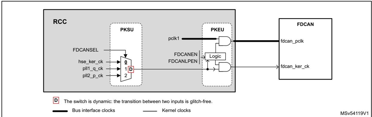
The diagram illustrates the clock distribution for the FDCAN module within the RCC (Reset and Clock Control) system. The RCC block contains two sub-modules: PKSU and PKEU. PKSU is a multiplexer that selects between three input clock sources: hse_ker_ck, pll1_q_ck, and pll2_p_ck, based on the FDCANSEL control signal. The selected clock is output as pclk1. PKEU is a logic block that takes pclk1 and two enable signals, FDCANEN and FDCANLPEN, as inputs. It generates two output clocks for the FDCAN module: fdcan_pclk (bus interface clock) and fdcan_ker_ck (kernel clock). The FDCAN module itself receives these two clocks. A legend indicates that thick lines represent bus interface clocks and thin lines represent kernel clocks. A note states that the switch in PKSU is dynamic and glitch-free. A footnote indicates that the 'D' on the multiplexer switch represents the selected input after a system reset.
RCC
PKSU
FDCANSEL
hse_ker_ck
pll1_q_ck
pll2_p_ck
0
1 D
2
pclk1
PKEU
FDCANEN
FDCANLPEN
Logic
FDCAN
fdcan_pclk
fdcan_ker_ck
D The switch is dynamic: the transition between two inputs is glitch-free.
Bus interface clocks
Kernel clocks
MSV54119V1
- 1. D represents the selected switch input after a system reset.
Clock distribution for graphic blocks (GPU2D, LTDC, DCMIPP and PSSI)
Figure 58. Clock distribution for GPU2D
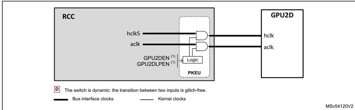
- 1. X represents the selected switch input after a system reset.
Figure 59. Clock distribution for LTDC and DCMIPP
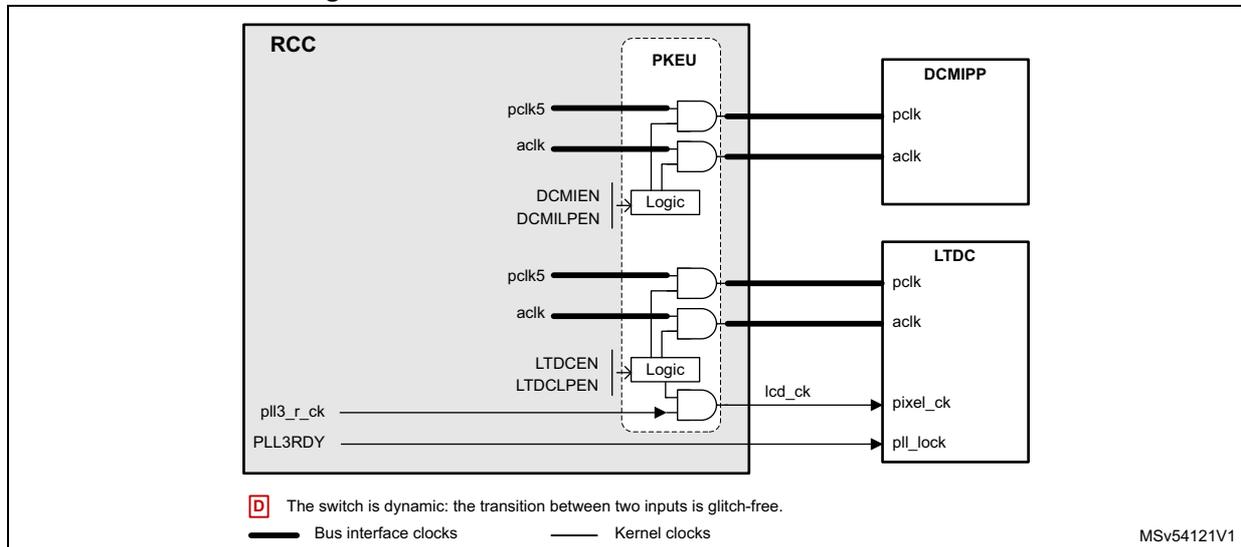
- 1. X represents the selected switch input after a system reset.
The PSSI receives an AHB clock and a kernel clock (pxclk).
The pxclk can be provided either by an external device via PSSI_PIXCK pad, or by the RCC. Note that the clock generated by the RCC is provided to pxclk input by the feedback path of the PSSI_PIXCK pad. The drive of the PSSI_PIXCK is controlled by the PSSI block.
Figure 60. Clock distribution for PSSI
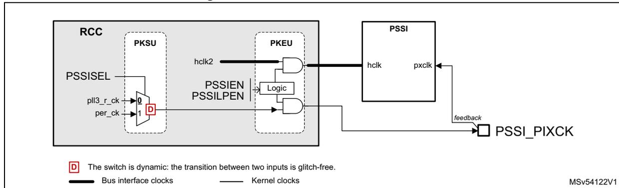
The diagram illustrates the clock distribution for the PSSI (Parallel Serial Interface) block. The RCC (Reset and Clock Control) block contains two sub-blocks: PKSU and PKEU. PKSU has three inputs: PSSISEL, pll3_r_ck, and per_ck. A dynamic switch (D) selects between pll3_r_ck (input 0) and per_ck (input 1). The output of this switch is connected to the PKEU block. PKEU has two inputs: hclk2 and a Logic block. The Logic block has two inputs: PSSIEP and PSSILPEN. The output of the Logic block is connected to the PSSI block. The PSSI block has two inputs: hclk and pxclk. The hclk input is connected to the output of the PKEU block. The pxclk input is connected to the output of the PSSI_PIXCK block. The PSSI_PIXCK block has a feedback loop from its output to its input. The legend indicates that the switch is dynamic (glitch-free) and that bus interface clocks are shown with a thick line, while kernel clocks are shown with a thin line.
- 1. X represents the selected switch input after a system reset.
Clock distribution for SDMMCs, FMC, and XSPIs
The FMC kernel clock can be chosen between 4 different sources, giving good flexibility.
For each XSPI, a clock switch allows the selection between 3 different sources, giving good flexibility. It is possible to enable independently each XSPI block.
The switches FMCSEL, XSPI[2:1]SEL, also embeds several protections:
- • In case of HSE failure detected by the HSECSS function, the XSPI[2:1]SEL switches and the FMCSEL switch go to recovery position in order to provide a default clock.
- • A protection bit: FMCCKP prevents the application to accidentally change the FMCSEL value. Refer to Section 7.5.7: Clock protection for details.
- • A protection bit: XSPICKP prevents the application to accidentally change the XSPI[2:1]SEL values. Refer to Section 7.5.7: Clock protection for details.
- • Status fields (FMCSWP, XSPI[2:1]SWP) located into RCC clock protection register (RCC_CKPROTR) allows the application to check the effective position of the switches.
- • If one of the switch is selecting an input with an invalid clock, the switch outputs a recovery clock preventing a memory crash and allowing the application to log or correct the issue. The RCC provides hclk5/4 as recovery clock. In order to work fine, the
application must ensure that the recovery clock frequency is supported by the external device.
- • For the XSPI[2:1]SEL switches:
- – Going to position 1 is allowed if PLL2ON = PLL2SEN = 1. If the application switches to position 1 when these conditions are not met, the switch generates the recovery clock.
- – Going to position 2 is allowed if PLL2ON = PLL2TEN = 1. If the application switches to position 2 when these conditions are not met, the switch generates the recovery clock.
- • For the FMCSEL switch:
- – Going to position 1 is allowed if PLL1ON = PLL1QEN = 1. If the application switches to position 1 when these conditions are not met, the switch generates the recovery clock.
- – Going to position 2 is allowed if PLL2ON = PLL2REN = 1. If the application switches to position 2 when these conditions are not met, the switch generates the recovery clock.
- – Going to position 3 is allowed if HSION = 1. If the application switches to position 3 when this condition is not met, the switch generates the recovery clock.
How to handle properly XSPI switches:
- • Switch on the wanted clock source,
- • Ensure the clock source is ready, and conditions described above are met,
- • Set XSPI1SEL to the wanted position,
- • Enable the XSPI clock (XSPIxEN = 1),
- • Read XSPISWP field from RCC_CKPROTR register,
- • If the position given by XSPISWP is the same as the wanted, it means that the XSPIx kernel clock is as expected.
- • If the position given by XSPISWP is 000, it means that there is no clock present at the selected input.
The XSPIs must provide a clock to the external memory, with a duty cycle distortion generally lower than 5%. In order to reach this requirement, the kernel clock provided to the XSPIs has a typical duty cycle of 50%. In addition, the XSPIs embed prescaler allowing clock division by even ratios.
Figure 61. Clock distribution for FMC, XSPIs, and MCEs
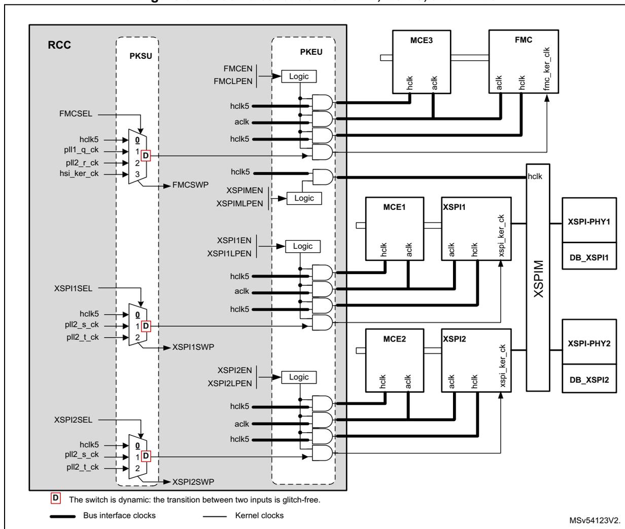
D The switch is dynamic: the transition between two inputs is glitch-free.
— Bus interface clocks — Kernel clocks
MSV54123V2.
- 1. X represents the selected switch input after a system reset.
The SDMMC1 and SDMMC2 share the same kernel clock. A clock switch allows the selection between 2 different sources. It is possible to enable independently each SDMMC block. Note that when one of the SDMMC is enabled via its SDMMC[2:1]EN bit, the associated delay block is enabled as well.
The application must take care about the duty-cycle of the kernel clock provided to the SDMMC blocks.
Table 66. SDMMC interface clock constraints
| SDMMC mode | Mode name | Interface clock frequency | Duty cycle constraint |
|---|---|---|---|
| SDIO | SDR12 | 25 MHz or less | 30 - 70% |
| SDR25 | 50 MHz or less | 30 - 70% | |
| DDR50 | 50 MHz or less | 45 - 55% | |
| SDR50 | 100 MHz or less | 30 - 70% |
Table 66. SDMMC interface clock constraints
| SDMMC mode | Mode name | Interface clock frequency | Duty cycle constraint |
|---|---|---|---|
| e.MMC | Backward compatible | 26 MHz or less | 30 - 70% |
| High Speed SDR | 52 MHz or less | 30 - 70% | |
| High Speed DDR | 52 MHz or less | 45 - 55% |
For example, if the SDMMC works in SDR50, then a kernel clock of 50 MHz, with a duty cycle better than 30-70% is enough. If the SDMMC works in DDR50, then it is recommended to provide a kernel clock of 100 MHz, and divide the frequency of the kernel clock by two, using the SDMMC divider in order to insure a duty-cycle very close to 50% for the SDMMC_CK.
Figure 62. Clock distribution for SDMMC[2:1] and DB_SDMMC[2:1]
![Clock distribution diagram for SDMMC[2:1] and DB_SDMMC[2:1] showing RCC, PKSU, PKEU, and various clock signals (hclk5, hclk2, sdmmc_hclk, sdmmc_ker_ck).](/RM0477-STM32H7Rx-7Sx/5f0934de7d51d5b287f8227e5deca80a_img.jpg)
The diagram illustrates the clock distribution for SDMMC[2:1] and DB_SDMMC[2:1] within the RCC (Reset and Clock Control) system. It shows the following components and signals:
- RCC (Reset and Clock Control):
The central block containing the clock distribution logic.
- PKSU (Power and Clock Switch Unit):
A sub-block within RCC that selects between two input clocks:
pll2_s_ck(input 0) andpll2_t_ck(input 1). The selection is controlled bySDMMC12SEL. The output of PKSU is a kernel clock signal. - PKEU (Power and Clock Enable Unit):
A sub-block within RCC that contains logic gates and enable signals for the SDMMC interfaces.
- For
SDMMC1
: Enabled by
SDMMC1ENandSDMMC1LPEN. It receiveshclk5(bus interface clock) and the kernel clock from PKSU. It outputssdmmc_hclk(bus interface clock) to DB_SDMMC1 and SDMMC1 , andsdmmc_ker_ck(kernel clock) to SDMMC1 . - For
SDMMC2
: Enabled by
SDMMC2ENandSDMMC2LPEN. It receiveshclk2(bus interface clock) and the kernel clock from PKSU. It outputssdmmc_hclk(bus interface clock) to DB_SDMMC2 and SDMMC2 , andsdmmc_ker_ck(kernel clock) to SDMMC2 .
- For
SDMMC1
: Enabled by
- PKSU (Power and Clock Switch Unit):
A sub-block within RCC that selects between two input clocks:
- External Components:
- DB_SDMMC1
and
SDMMC1
: Receive
hclk(bus interface clock) andsdmmc_hclk(bus interface clock) from PKEU. SDMMC1 also receivessdmmc_ker_ck(kernel clock). - DB_SDMMC2
and
SDMMC2
: Receive
hclk(bus interface clock) andsdmmc_hclk(bus interface clock) from PKEU. SDMMC2 also receivessdmmc_ker_ck(kernel clock).
- DB_SDMMC1
and
SDMMC1
: Receive
Legend:
- D : The switch is dynamic: the transition between two inputs is glitch-free.
- Bus interface clocks : Represented by thick lines.
- Kernel clocks : Represented by thin lines.
MSv54124V1
- 1. X represents the selected switch input after a system reset.
Clock distribution for OTGFS, OTGHS and UCPD
Figure 63 shows the clock distribution for the USB blocks.
- • The USB type-C power delivery block (UCPD), uses ucpd_ker_ck as kernel clock. The ucpd_ker_ck is directly generated from the HSI output divided by 4.
- • The USBPHYC, embeds a PLL accepting a reference input frequency of 16, 19.2, 20, 24, 26 or 32 MHz. The reference clock can be selected among:
- – hse_osc_ck
- – hse_ker_ck/2 or
- – pll3_q_ck
The USBPHYC provides a 60 MHz clock to the OTGHS block, and a 48 MHz clock to the OTGFS block. The clock hse_osc_ck is the direct output of the HSE oscillator.
- • The OTGHS receives the 60 MHz clock from the USBPHYC ( phy60m_ck ), when working in HS or FS mode.
- • The OTGFS receives a 48 MHz clock. The application can select:
- – the clk48mohci (from USBPHYC)
- – the hsi48_ker_ck for crystal-less applications
- – hse_ker_ck or
- – pll3_q_ck
The selection of the reference clock for the USBPHYC is performed by a simple MUX. In order to change the clock source, the application must follow the sequence hereafter:
- • Disable the USBPHYC clock by setting USBPHYCEN to 0
- • Change the clock source selector (USBPHYCSEL) to the wanted value
- • Enable the USBPHYC clock by setting USBPHYCEN to 1.
Figure 63. Clock distribution for USB and UCPD
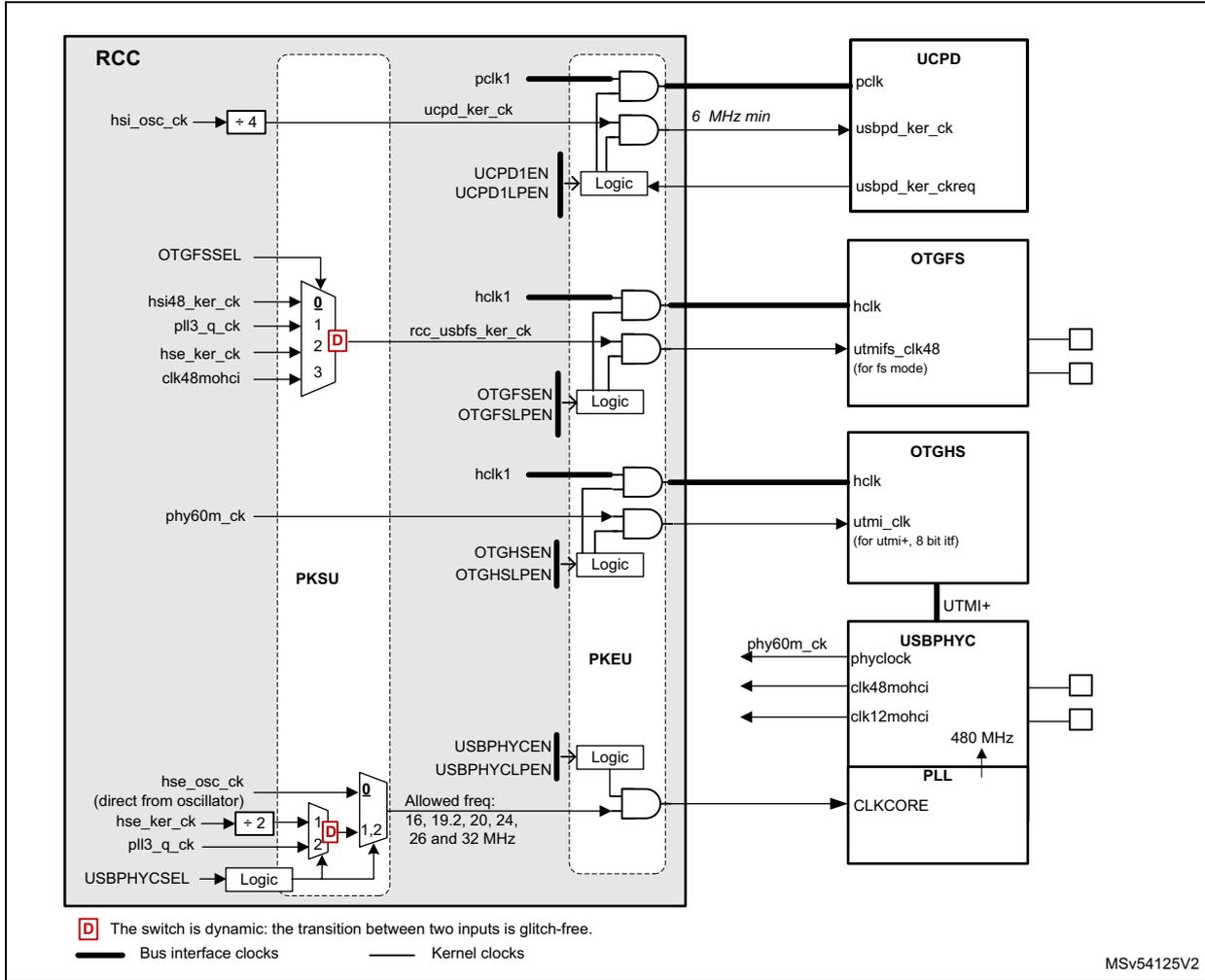
The diagram illustrates the clock distribution for USB and UCPD within the RCC (Reset and Clock Control) system. It shows the flow of various clock signals from the RCC to different USB-related components.
- RCC (Reset and Clock Control):
The central component containing internal logic and switches.
- UCPD:
Receives
pclk1anducpd_ker_ck.ucpd_ker_ckis derived fromhsi_osc_ck(divided by 4). A logic block combinesUCPD1ENandUCPD1LPENto control the output. A note indicates a minimum frequency of 6 MHz. - OTGFS:
Receives
hclk1andrcc_usbfs_ker_ck.rcc_usbfs_ker_ckis selected via a dynamic switch (marked with 'D') fromhsi48_ker_ck,pll3_q_ck,hse_ker_ck, orclk48mohci. A logic block combinesOTGFSSENandOTGFSLPEN. - OTGHS:
Receives
hclk1andphy60m_ck. A logic block combinesOTGHSENandOTGHSLPEN. - USBPHYC:
Receives
phy60m_ck,clk48mohci, andclk12mohci. These are controlled by a logic block combiningUSBPHYCENandUSBPHYCLPEN. - PLL:
Receives
CLKCORE, which is derived fromhse_osc_ck(direct from oscillator),hse_ker_ck(divided by 2), orpll3_q_ck. This selection is controlled by a dynamic switch (marked with 'D') andUSBPHYCSEL. Allowed frequencies are 16, 19.2, 20, 24, 26, and 32 MHz.
- UCPD:
Receives
- PKSU and PKEU: Sub-blocks within the RCC containing logic gates (AND/OR) that enable the clock signals to the external components.
- External Components:
- UCPD: USB-C Power Delivery controller.
- OTGFS:
On-The-Go Full-Speed controller. Output
utmiifs_clk48is for FS mode. - OTGHS:
On-The-Go High-Speed controller. Output
utmi_clkis for UTMI+ 8-bit IF. - USBPHYC:
USB PHY controller. Output
480 MHzis connected to the PLL. - PLL: Phase-Locked Loop for clock generation.
Legend:
- D The switch is dynamic: the transition between two inputs is glitch-free.
- Bus interface clocks
- Kernel clocks
MSV54125V2
- 1. X represents the selected switch input after a system reset.
Clock distribution for ETH1
The Ethernet clocks provided by the RCC are available on ETH_CLK pad. The application can select if the ETH_CLK is generated from the HSE kernel clock or from the pll3_s_ck .
The RCC also provides the bus clock and the reference clock for the PTP function.
Note that the bus and PTP clocks generation are controlled via ETH1MACEN and ETH1MACLPEN bits.
Figure 64. Clock distribution for ETH1
![Figure 64. Clock distribution for ETH1. This block diagram shows the internal clocking architecture of the RCC for the ETH1 interface. On the left, external pads are shown: ETH_MII_TX_CLK, ETH_MII_RX_CLK/ETH_RMII_REF_CLK, and ETH_CLK. The RCC block contains a PKSU section with a PLL (hse_ker_ck, pll3_s_ck) and a divider (÷ 2, 20). A switch (D) selects between MII (orange) and RMII (blue) paths based on ETH_SEL (from SBS). Logic blocks (PKEU) generate control signals (ETH1TXEN, ETH1TXLPEN, ETH1RXEN, ETH1RXLPEN, ETH1MACEN, ETH1MACLPEN) for the ETH1 block. The ETH1 block outputs various clocks: clk_tx_i (MII tx clock 2.5/25), mac_speed_o[1:0], clk_rx_i (MII rx clock 2.5/25), clk_rmii_i (RMII reference clock 50 MHz), hclk, and clk_ptp_ref_i. A legend at the bottom defines the line colors: orange for MII, blue for RMII, thick black for bus interface clocks, and thin black for kernel clocks. A note indicates that the switch is dynamic and glitch-free. The diagram is labeled MSV54126V2.](/RM0477-STM32H7Rx-7Sx/3f545bcad6d16c7914c7ca7323f5358f_img.jpg)
- 1. X represents the selected switch input after a system reset.
The signal ETH_SEL is provided by the SBS block and defines the interface type used:
In MII mode (orange path):
- • The transmit clock is received from the external PHY via the pad ETH_MII_TX_CLK.
- • The receive clock is received from the external PHY via the pad ETH_MII_RX_CLK.
- • The clock frequency is 2.5 MHz for Ethernet at 10 Mbps or 25 MHz for Ethernet at 100 Mbps.
In RMI mode (blue path):
- • The reference clock (50 MHz) can be selected between several sources:
- – The ETH_RMII_REF_CLK pad, if the reference clock is provided by the PHY
- – The hse_ker_ck in case the Ethernet PHY is providing a reference clock connected to OSC_IN
- – The ETH_CLK feedback clock (eth_clk_fb) if the RCC is providing the reference clock to the PHY. This selection is controlled via ETH1REFCKSEL[1:0].
- • The ETH_SEL must be set to 1,
- – a clock must be provided to clk_rx_i and clk_tx_i inputs
- – The clock frequency at clk_rx_i and clk_tx_i inputs is 2.5 MHz (division by 20) for Ethernet at 10 Mbps, and 25 MHz (division by 2) for Ethernet at 100 Mbps.
- – The transmit and receive clock frequency can be adjusted dynamically to 2.5 or 25 MHz according to the signal mac_speed_o[0] provided by the ETH block.
Note that the ETH1REFCKSEL mux position cannot be changed when a clock is provided to the ETH1 block. In order to select the wanted mux position the following sequence must be respected:
- • Set bits ETH1TXEN, ETH1RXEN and ETH1MACEN to 0,
- • Set ETH1REFCKSEL to the wanted position,
- • Set bits ETH1TXEN, ETH1RXEN and ETH1MACEN to 1
The RCC can generate a reference clock of 25 or 50 MHz to the external PHY, via ETH_CLK pad. The figure hereafter shows the possible clock configurations.
The ETH_CLK is generated only if:
- • ETH1TXEN or ETH1RXEN are enabled, and
- • the system is in Run or Sleep, and
- • the clock source selected by ETH1PHYCKSEL is available.
The bits ETH1REFCKSEL[1:0] and ETH1PHYCKSEL are located into the RCC AHB peripheral kernel clock selection register (RCC_CCIPR1) .
Figure 65. ETH clock configuration
![Figure 65. ETH clock configuration. The diagram shows two configurations for Ethernet PHY and Microcontroller clock connections. The left configuration shows the PHY connected to the Microcontroller's ETH_RMII_REF_CLK pad, with ETH1REFCKSEL[1:0] = 0. The right configuration shows the PHY connected to the Microcontroller's OSC_IN pad, with ETH1REFCKSEL[1:0] = 1. Both configurations show the PHY connected to the Microcontroller's OSC_OUT pad, with ETH1REFCKSEL[1:0] = 2.](/RM0477-STM32H7Rx-7Sx/e66dfa4e9baa30fef4fd55f5657355fb_img.jpg)
The diagram illustrates two clock configuration scenarios for an Ethernet PHY connected to a Microcontroller. In the left scenario, the PHY's reference clock input is connected to the Microcontroller's ETH_RMII_REF_CLK pad, and the register setting is ETH1REFCKSEL[1:0] = 0. In the right scenario, the PHY's reference clock input is connected to the Microcontroller's OSC_IN pad, and the register setting is ETH1REFCKSEL[1:0] = 1. Both scenarios show the PHY connected to the Microcontroller's OSC_OUT pad, with the register setting ETH1REFCKSEL[1:0] = 2. The diagram includes labels for 'Ethernet PHY', 'Microcontroller', 'ETH_RMII_REF_CLK', 'OSC_IN', 'OSC_OUT', and 'ETH_CLK'.
The ETH1 block provides information on the MAC speed (mac_speed_o[1:0]), which may change dynamically:
- • mac_speed_o[1:0] = 0b10: for 10 Mbps
- • mac_speed_o[1:0] = 0b11 or 0b0x: for 100 Mbps
Clock distribution for ADC1-2
Figure 66. Clock distribution For ADCs
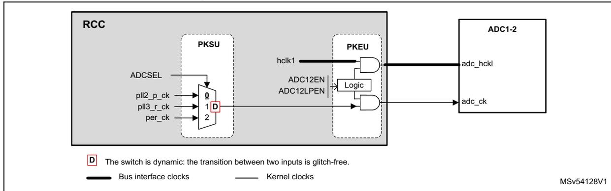
- 1. X represents the selected switch input after a system reset.
Clock distribution for SAES and RNG
Figure 67. Clock distribution for SAES and RNG
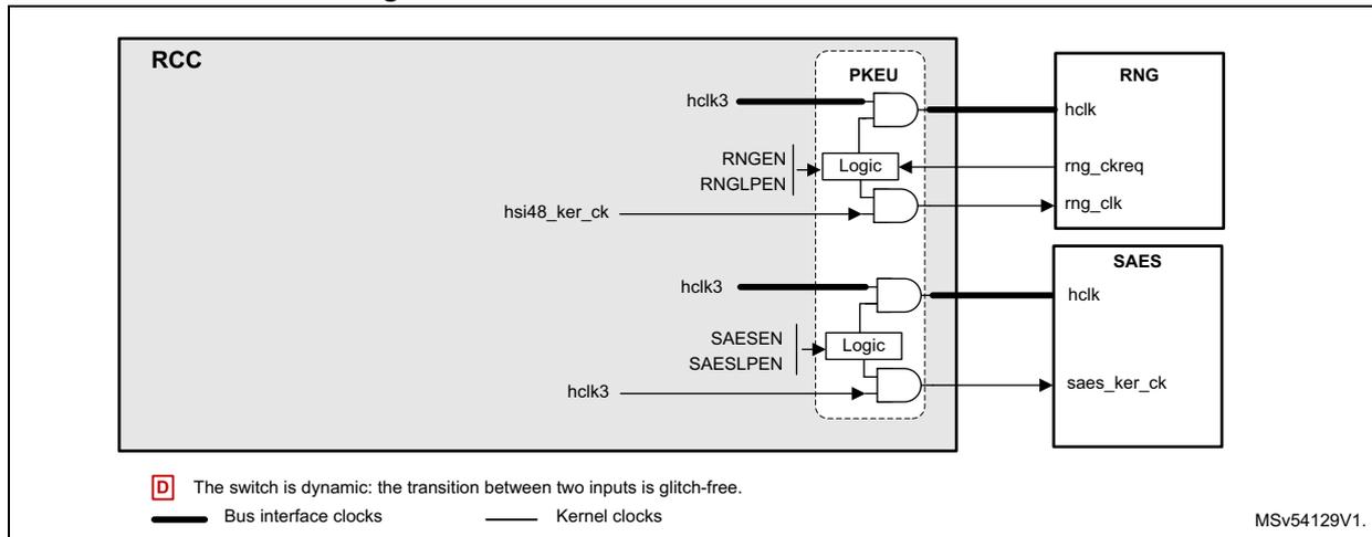
- 1. X represents the selected switch input after a system reset.
The RNG block is using the hsi48_ker_ck as kernel clock. The logic handling controlling the clock of the RNG is different from standard peripherals. When enabled, the RNG has to assert its kernel clock request, in order to get a kernel clock. For example, if the SAES needs the RNG resource, the RNG must also be enabled. Refer to Section 7.5.12: Peripheral clock gating control for details.
Clock distribution for HDMI-CEC
Figure 68. Clock distribution for HDMI-CEC
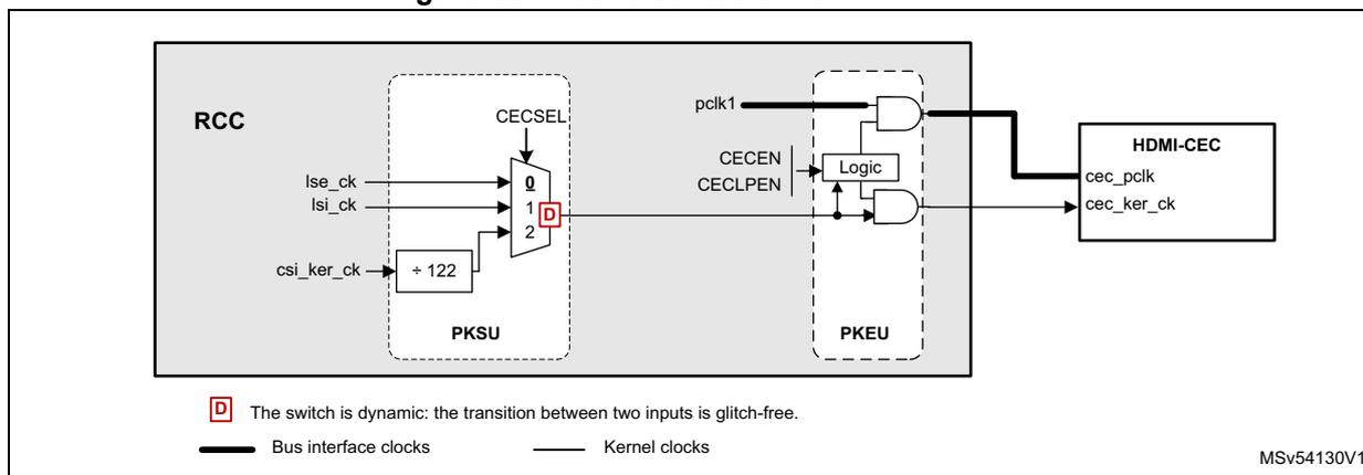
- 1. X represents the selected switch input after a system reset
Clock distribution for TIM and LPTIM
The TIMs timers are using kernel clocks (tim_ker_ck) phase aligned with the bus interface clock.
The working frequency of the timers clock depends on:
- • The APB prescaler corresponding to the bus where the timer is connected, and
- • The bit TIMPRE
Figure 69. Clock distribution for TIMs
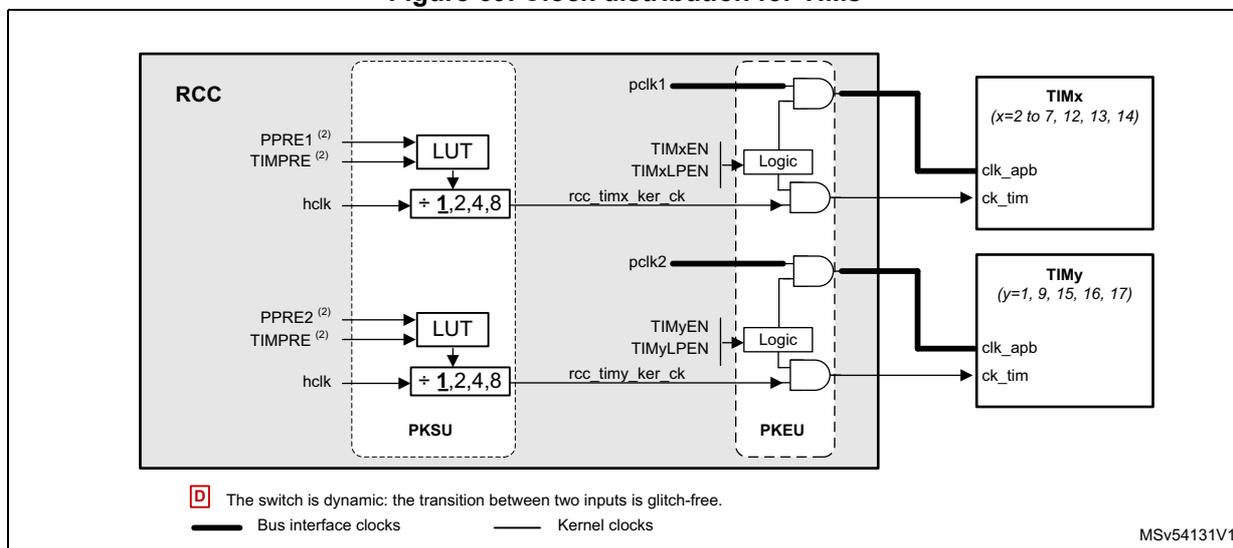
- 1. X represents the selected switch input after a system reset
- 2. Can be changed on the fly
The Table 67 shows how to select the timer clock frequency.
Table 67. Ratio between clock timer and pclk
| PPRE1
(1) PPRE2 | TIMPRE (2) | - | F
rcc_timx_ker_ck F rcc_timy_ker_ck | F
pclk1 F pclk2 | Comments |
|---|---|---|---|---|---|
| 0xx | x | → | F hclk1 | F hclk1 | The timer clock is equal to the bus clock. |
| 100 | x | → | F hclk1 | F hclk1 / 2 | The timer clock is twice as fast as the bus clock. |
| 101 | 0 | → | F hclk1 / 2 | F hclk1 / 4 | |
| 110 | 0 | → | F hclk1 / 4 | F hclk1 / 8 | |
| 111 | 0 | → | F hclk1 / 8 | F hclk1 / 16 | The timer clock is 4 times faster than the bus clock. |
| 101 | 1 | → | F hclk1 | F hclk1 / 4 | |
| 110 | 1 | → | F hclk1 / 2 | F hclk1 / 8 | |
| 111 | 1 | → | F hclk1 / 4 | F hclk1 / 16 |
- 1. PPRE1 and PPRE2 are the prescaler for the APB1 and APB2 clocks.
- 2. TIMPRE belongs to RCC clock configuration register (RCC_CFGR) .
The LPTIMs timers have a kernel clocks fully asynchronous with respect to their bus interface clock. The kernel clock can be selected among up to 6 clock sources.
The LPTIMs also use lse_ck and lsi_ck as kernel clock, allowing them to work even when the system is in Stop mode.
Figure 70. Clock distribution for LPTIMs
![Schematic diagram of clock distribution for LPTIMs. It shows three LPTIM blocks (LPTIM1, LPTIM[3:2], LPTIM[5:4]) connected to RCC and PKSU domains via multiplexers and logic gates. The diagram includes clock sources like pclk1, pclk2_p_ck, pclk3_r_ck, lse_ck, lsi_ck, and per_ck. A legend at the bottom explains the symbols for dynamic switches and clock types.](/RM0477-STM32H7Rx-7Sx/c658c99fa8ab58a4c0ab2f269a24a950_img.jpg)
The diagram illustrates the clock distribution for LPTIMs. It is divided into three main sections for LPTIM1, LPTIM[3:2], and LPTIM[5:4]. Each section consists of a multiplexer (MUX) in the RCC domain, a logic gate in the PKSU domain, and the LPTIM block itself. The MUX selects between various clock sources based on configuration bits (LPTIM1SEL, LPTIM23SEL, LPTIM45SEL). The output of the MUX is connected to one input of an AND gate in the PKSU domain. The other input of the AND gate is connected to a 'pclk' signal (pclk1 for LPTIM1, pclk4 for the others). The output of the AND gate is connected to the LPTIM block. The LPTIM block also receives 'lptim_pclk' and 'lptim_ker_ck' signals. The diagram also shows the RCC and PKSU domains, and the connection between them. A legend at the bottom indicates that a 'D' in a box represents a dynamic switch, a thick line represents a bus interface clock, and a thin line represents a kernel clock.
1. X represents the selected switch input after a system reset
Clock distribution for RTC/AWU clock
The rtc_ck clock source can be one of the following:
- • the hse_rtc_ck ( hse_ker_ck divided by a programmable prescaler)
- • the lse_ck
- • the lsi_ck clock
The source clock is selected by programming the RTCSEL[1:0] bits in the RCC Backup domain control register (RCC_BDCR) and the RTCPRE[5:0] bits in the RCC clock configuration register (RCC_CFGR) .
This selection cannot be modified without resetting the Backup domain.
Figure 71. Clock distribution for RTC
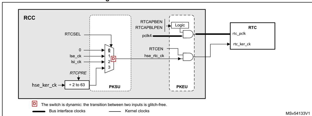
- 1. X represents the selected switch input after a system reset
If the LSE is selected as RTC clock, the RTC works normally even if the backup or the \( V_{DD} \) supply disappears.
The LSE clock is in the Backup domain, whereas the other oscillators are not. As a consequence:
- • If LSE is selected as RTC clock, the RTC continues working even if the \( V_{DD} \) supply is switched OFF, provided the \( V_{BAT} \) supply is maintained.
- • If LSI is selected as the RTC clock, the AWU state is not guaranteed if the \( V_{DD} \) supply is powered off.
- • If the HSE clock is used as RTC clock, the RTC state is not guaranteed if the \( V_{DD} \) supply is powered off or if the \( V_{CORE} \) supply is powered off. In addition the HSE is not available if the system goes to Stop.
The rtc_ck clock is enabled through RTCEN bit located in the RCC Backup domain control register (RCC_BDCR) .
The RTC bus interface clock (APB clock) is enabled through RTCAPBEN and RTCAPBLPEN bits located in RCC_APB4ENR/LPENR registers.
Note: To read the RTC calendar register when the APB clock frequency is less than seven times the RTC clock frequency ( \( F_{APB} < 7 \times F_{RTCLCK} \) ), the software must read the calendar time and date registers twice. The data are correct if the second read access to RTC_TR gives the same result than the first one. Otherwise a third read access must be performed.
Clock distribution for watchdog
The RCC provides the clock for the two watchdog blocks available on the circuit. The independent watchdog (IWDG) is connected to the LSI. The window watchdog (WWDG) is connected to the APB clock.
If an independent watchdog is started by either hardware option or software access, the LSI is forced ON and cannot be disabled. After the LSI oscillator setup delay, the clock is provided to the IWDG.
The window watchdog clock (pclk1) can be enabled by setting the WWDGEN bit in RCC_APB1ENR register. The software cannot stop WWDG down-counting by setting WWDGEN bit to '0'.
The WWDG block is frozen when the MCU goes to Stop mode.
Figure 72. Clock distribution for WWDG and IWDG
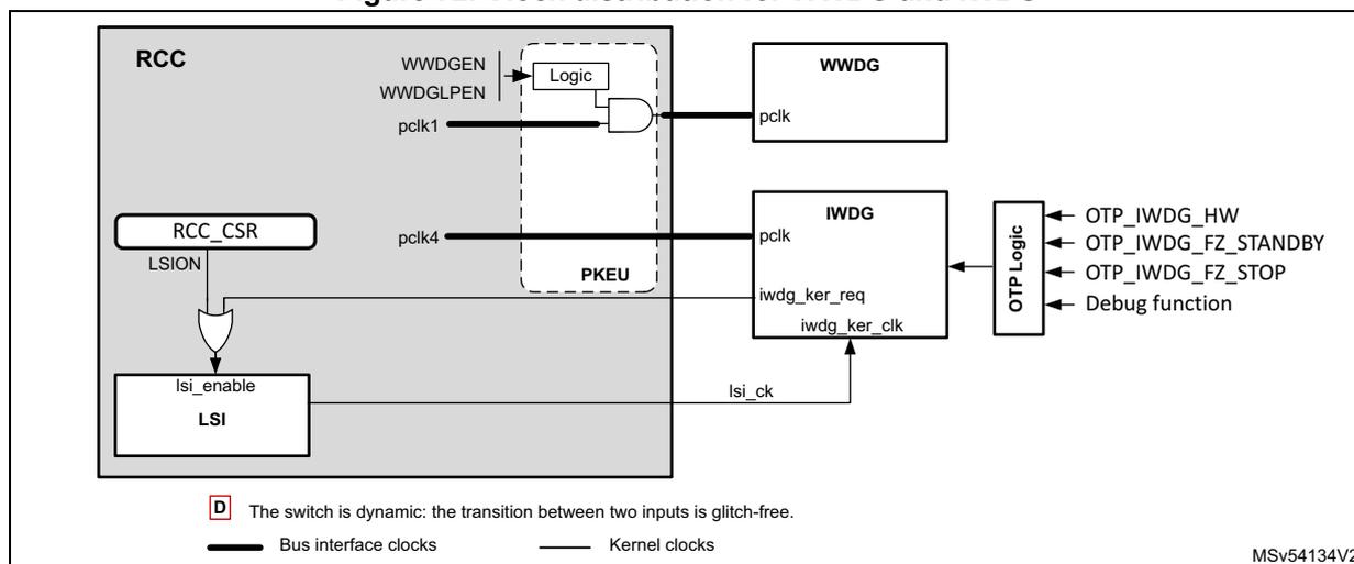
D The switch is dynamic: the transition between two inputs is glitch-free.
Bus interface clocks Kernel clocks
MSV54134V2
- 1. X represents the selected switch input after a system reset
Clock distribution for Debug and Trace
The clock generation for the trace and debug is controlled by the DBGMCU block. The DBGCKEN bit allows the application to provide a clock to the debug components. It is also possible to enable this clock via the Debug Access Port.
The trace clock generation is controlled via TRACECKEN bit.
Figure 73. Clock distribution for DBG and trace
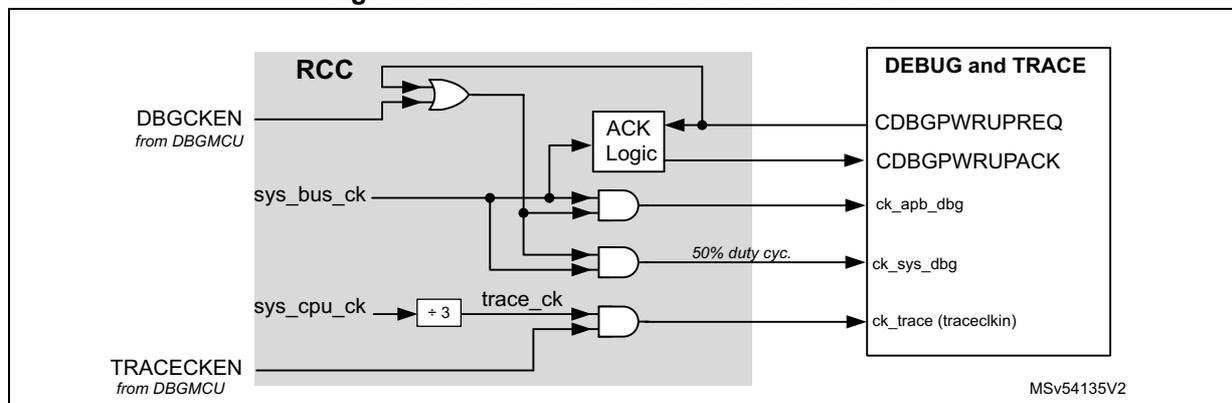
MSV54135V2
- 1. X represents the selected switch input after a system reset
Clock frequency measurement using TIMx
Most of the clock source generator frequencies can be measured by means of the input capture of TIMx.
- • Calibrating the HSI or CSI with the LSE:
The primary purpose of having the LSE connected to a TIMx input capture is to be able to accurately measure the HSI or CSI. This requires to use the HSI or CSI as system clock source either directly or via PLL1. The number of system clock counts between
consecutive edges of the LSE signal gives a measurement of the internal clock period. Taking advantage of the high precision of LSE crystals (typically a few tens of ppm) we can determine the internal clock frequency with the same resolution, and trim the source to compensate for manufacturing-process and/or temperature- and voltage-related frequency deviations.
The basic concept consists in providing a relative measurement (e.g. HSI/LSE ratio). The precision is therefore tightly linked to the ratio between the two clock sources. The greater the ratio is, the more accurate the measurement is.
The HSI and CSI oscillators have dedicated user-accessible calibration bits for this purpose (see RCC CSI calibration register (RCC_CSICFGR) ). When HSI or CSI is used via the PLLx, the system clock can also be fine-tuned by using the fractional divider of the PLLs.
- • Calibrating the LSI with the HSI:
The LSI frequency can also be measured: this is useful for applications that do not have a crystal. The ultra-low-power LSI oscillator has a large manufacturing process deviation. The LSI clock frequency can be measured using the more precise HSI clock source. Using this measurement, a more accurate RTC time base timeouts (when LSI is used as the RTC clock source) and/or an IWDG timeout with an acceptable accuracy can be obtained.
7.5.10 General clock concept overview
The RCC handles the distribution of the CPU, bus interface and peripheral clocks for the system, according to the CPU operating mode (refer to Section 7.5.1: Clock naming convention for details on clock definitions).
For each peripheral, the application can control the activation/deactivation of its kernel and bus interface clock. Prior to use a peripheral, the CPU must enable it (by setting PERxEN to 1), and define if this peripheral remains active in Sleep mode (by setting PERxLPEN to 1). This is called 'allocation' of a peripheral by the CPU (refer to Section 7.5.11: Peripheral allocation for more details).
The peripheral allocation is used:
- • by the RCC to automatically control the clock gating according to the CPU modes, and
- • by the PWR to control the supply voltages of VCORE.
Memory handling
The CPU can access all the memory areas available in the product:
- • AXISRAM1, AXISRAM2, AXISRAM3, AXISRAM4, ITCM, DTCM1, DTCM2 and FLASH
- • AHBSRAM1 and AHBSRAM2
- • BKPRAM
The BKPRAM, AHBSRAM1 and AHBSRAM2 have dedicated enable bits in order to gate the bus interface clock. The CPU needs to enable them prior to use these memories.
Note: The memory interface clocks (Flash memory and RAM interfaces) can be stopped by software during Sleep mode (via SRAMyLPEN bits).
Refer to Section 7.5.12: Peripheral clock gating control and Section 7.5.13: CPU and bus matrix clock gating control sections for details on clock enabling.
7.5.11 Peripheral allocation
The CPU can allocate a peripheral and hence control its kernel and bus interface clock.
The CPU can allocate a peripheral by setting the dedicated PERxEN bit to 1.
The CPU can control the peripheral clocks gating when it is in Sleep mode via the PERxLPEN bits.
Refer to for additional information.
The peripheral allocation bits (PERxEN bits) are used by the hardware to provide the kernel and bus interface clocks to the peripherals. However they are also used to link peripherals to the CPU. In this way, the hardware is able to safely gate the peripheral clocks and bus matrix clocks according to CPU states.
Clock switches and gating
- • Clock switching delays
The input selected by the clock switches can be changed dynamically without generating spurs or timing violation. For example, if PERxSEL (In Figure 74 ) goes from 0 to 1, the switch first disables the clock output using the currently selected clock (in0_ck), and enables again the clock output using the new selected clock (in1_ck). The disable and enable commands are re-synchronized to their respective clocks. If one of the the two clocks are not present, the sequence cannot be completed, and no clock is output. To recover from this situation, the user must either provide a valid clock to in1_ck input or set back PERxSEL to 0.
During the transition from one input to another, the kernel clock provided to the peripheral is gated, in the worst case, during 2 or 3 clock cycles of the new selected clock. As shown in Figure 74 , both input clocks must be present during transition time.
Figure 74. Kernel clock switching
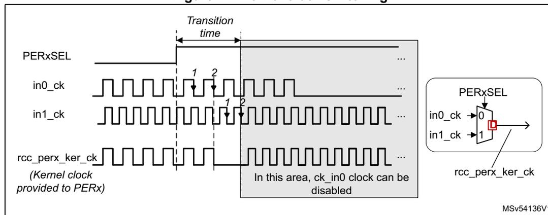
The diagram illustrates the timing of kernel clock switching. The top signal, PERxSEL, is a control signal that switches from 0 to 1 at a specific 'Transition time'. Below it, in0_ck and in1_ck are input clocks. The third signal, rcc_perx_ker_ck, is the kernel clock provided to the peripheral. The diagram shows that during the transition, the kernel clock is gated. A shaded area indicates that in this area, ck_in0 clock can be disabled. An inset shows a multiplexer (MUX) with inputs in0_ck (0) and in1_ck (1), controlled by PERxSEL, outputting rcc_perx_ker_ck. The MUX has a delay element (D) in the output path.
- • Clock enabling delays
In the same way, the clock gating logic synchronizes the enable command (coming generally from a kernel clock request or PERxEN bits) with the selected clock, in order to avoid generation of spurs.
- – A maximum delay of two periods of the enabled clock may occur between the enable command and the first rising edge of the clock. The enable command can
be the rising edge of the PERxEN bits of RCC_xxxxENR registers, or a kernel clock request asserted by a peripheral.
- – A maximum delay of 1.5 periods of the disabled clock may occur between the disable command and the last falling edge of the clock. The disable command can be the falling edge of the PERxEN bits of RCC_xxxxENR registers, or a kernel clock request released by a peripheral.
Note: Both the kernel and bus interface clocks are affected by this re-synchronization delay.
7.5.12 Peripheral clock gating control
As mentioned previously, each peripheral requires one or several bus interface clock, named rcc_perx_bus_ck (for peripheral 'x'). These clocks can be an APB, AHB or AXI clock, according to which bus or busses, the peripheral is connected.
The clocks used as bus interface for peripherals, can be aclk , hclk[5:1] , pclk[5:4] , or pclk[2:1] , depending on the bus connected to each peripheral.
Some peripherals also require dedicated clocks for their communication interface. These clocks are generally asynchronous with respect to the bus interface clock. They are named kernel clocks ( perx_ker_ck ). Both bus interface and kernel clocks can be gated according to several conditions detailed hereafter.
As shown in Figure 75 , enabling the kernel and bus interface clocks of each peripheral depends on several input signals:
- • PERxEN and PERxLPEN bits,
PERxEN represents the peripheral enable (allocation) bit for the CPU. The CPU can write these bits to 1 via the RCC_xxxxENR registers. - • CPU state ( cpu_sleep and cpu_deepsleep signals)
- • Kernel clock request ( perx_ker_ckreq ) of the peripheral itself, when the feature is available
Refer to Section 7.5.11: Peripheral allocation for more details.
Figure 75. Peripheral kernel clock enable logic details
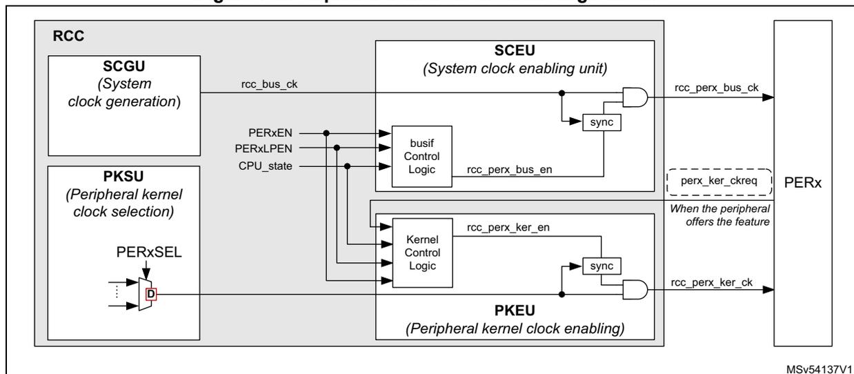
Table 68 gives a detailed description of the enabling logic of the peripheral clocks for peripherals located in the CPU domain and allocated by the CPU.
Table 68. Peripheral clock enabling
| PERxEN | PERxLPEN | PERxSEL | perx_ker_ckreq | CPU state | rcc_perx_ker_ck | rcc_perx_bus_ck | Comments |
|---|---|---|---|---|---|---|---|
| 0 | X | X | X | X | - | - | No clock provided to the peripheral, because PERxEN=0 |
| 1 | X | X | X | Run | CK | CK | Kernel and bus interface clocks are provided to the peripheral, because the CPU is in Run, and PERxEN = 1. |
| 1 | 0 | X | X | Sleep | - | - | No clock provided to the peripheral, because the CPU is in Sleep and PERxLPEN = 0 |
| 1 | 1 | CK | CK | Kernel and bus interface clocks are provided to the peripheral, because CPU is in Sleep, and PERxLPEN = 1 | |||
| 1 | 0 | X | X | Stop | - | - | No clock provided to the peripheral because the PERxLPEN bit is set to 0. |
| 1 | 1 | no lsi_ck and no lse_ck and no hsi_ker_ck and no csi_ker_ck | X | - | - | No clock provided to the peripheral because CPU is in Stop and lse_ck or lsi_ck or hsi_ker_ck or csi_ker_ck are not selected as kernel clock. | |
| 1 | 1 | lsi_ck or lse_ck | X | CK | - | Kernel clock is provided to the peripheral because: PERxEN = PERxLPEN = 1 and lsi_ck or lse_ck are selected and enabled. The bus interface clock is not provided as the CPU is in Stop. | |
| 1 | 1 | hsi_ker_ck or csi_ker_ck | 1 | CK | - | Kernel clock is provided to the peripheral because: req_ker_perx = 1, and PERxEN = PERxLPEN = 1 and hsi_ker_ck or csi_ker_ck are selected and enabled. The bus interface clock is not provided as the CPU is in Stop. | |
| 1 | 1 | hsi_ker_ck or csi_ker_ck | 0 | - | - | No clock provided to the peripheral because CPU is in Stop, and no kernel clock request pending |
As a summary, we can state that the kernel clock is provided to the peripherals when the following conditions are met:
- 1. The CPU is in Run mode, and the peripheral is enabled.
- 2. The CPU is in Sleep mode and the peripheral is enabled with PERxLPEN = 1.
- 3. The CPU is in Stop mode, the peripheral is enabled with PERxLPEN = 1, the peripheral generates a kernel clock request and the selected clock is hsi_ker_ck or csi_ker_ck .
- 4. The CPU is in Stop mode, the peripheral is enabled with PERxLPEN = 1 and the kernel source clock of the peripheral is lse_ck or lsi_ck .
The bus interface clock is provided to the peripherals only when conditions 1 or 2 are met.
The RNG block is not clocked as other peripherals, the table hereafter shows the way RNG is clocked.
Table 69. RNG clock enabling
| RNGEN | RNGLPEN | rng_ker_ckreq | CPU state | hsi48_ker_ck | rcc_rng_hclk3 | Comments |
|---|---|---|---|---|---|---|
| 0 | X | X | X | - | - | No clock provided to the peripheral, because RNGEN=0 |
| 1 | X | 0 | Run | - | CK | hsi48_ker_ck not provided because the kernel clock request is not asserted. hclk3 clock is provided |
| 1 | X | 1 | CK | CK | Both hsi48_ker_ck and hclk3 are provided because the kernel clock request is asserted, and RNGEN = 1. | |
| 1 | 0 | X | Sleep | - | - | No clock provided, because the CPU is in Sleep and RNGLPEN = 0 |
| 1 | 1 | 0 | - | CK | hsi48_ker_ck not provided because the kernel clock request is not asserted. hclk3 clock is provided | |
| 1 | 1 | 1 | CK | CK | Both hsi48_ker_ck and hclk3 are provided because the kernel clock request is asserted, RNGEN = 1 and RNGLPEN = 1 | |
| 1 | X | X | Stop | - | - | No clock provided because the CPU is in Stop mode |
7.5.13 CPU and bus matrix clock gating control
The clocks of the CPU, AHB and AXI bridges and APB busses are enabled according to the rules hereafter:
- • The CPU clock ( rcc_cpu_ck ) is enabled when the CPU is in Run or Sleep mode.
- • The AXI bridge clock is enabled when the CPU is in Run or Sleep mode.
- • Each AXI master and slave has an independent clock gating activated by default, to further reduce the power consumption. When activated the clock is automatically enabled on bus transaction request. The RCC AXI clocks gating disable register (RCC_CKGDISR) allows the application to control this behavior.
- • The AHB bus matrix clock is enabled if one of the following conditions is met:
- – The CPU is in Run mode
- – The CPU is in Sleep mode, and at least one peripheral connected to this bridge have both its PERxEN and PERxLPEN set to 1.
- – The CPU is in Sleep mode, and AHB1, AHB2, AHB3, AHB4 or AHB5 has its clock enabled
- • The clocks of the bridges AHB1, 2, 3, 4, 5 are enabled when one of the following conditions is met:
- – The CPU is in Run mode.
- – The CPU is in Sleep mode with at least one peripheral connected to this bus having both its PERxEN and PERxLPEN set to 1.
- – The CPU is in Sleep mode and the APB bus connected to the AHB bridge has its clock enabled.
- • The APB1, 2, 4, 5 clock busses are enabled when one of the following conditions is met:
- – The CPU is in Run mode.
- – When the CPU is in Sleep mode with at least one peripheral connected to this bus having both its PERxEN and PERxLPEN set to 1.
7.5.14 Low-power emulation modes
In order to ease the debugging of the circuit, the RCC is able to handle an emulation mode for Stop and Standby modes.
Sleep emulation mode
The Sleep emulation mode is controlled by the DBG_SLEEP bit of the DBGMCU_CR register. When the processor goes to Sleep with DBG_SLEEP = 1, then the processor clock, the clocks of all enabled peripherals, debug parts, and interconnect are maintained activated.
Stop emulation mode
The Stop emulation mode is controlled by the DBG_STOP bit of DBGMCU_CR register. When the processor goes to Stop with DBG_STOP = 1, then:
- • The PWR and the RCC remains activated.
- • The VDDCORE voltage is set to the minimum VOS value.
- • The RCC selects HSI or CSI as system clock, depending on STOPWUCK bit.
- • The processor clock is gated (rcc_cpu_ck, see Figure 51 ),
- • The free-running clock is generated (rcc_fclk, see Figure 51 ), and all the debug parts remain clocked.
- • All peripheral clocks are gated. Peripherals can still receive a kernel clock if they request it, and if the kernel clock source is an RC oscillator. They also receive the kernel clock if the kernel clock source is LSI or LSE.
- • The interconnect clocks are gated.
When a wake-up event occurs:
- • The VDDCORE voltage remains to the minimum VOS value.
- • The peripheral waking up the system sends the interrupt to the NVIC via the EXTI.
- • The CPU exits from STOP and the RCC provide the processor clock and interconnect clocks.
Standby emulation mode
The Standby emulation mode is controlled by the DBG_STANDBY bit of the DBGMCU_CR register.
When the system goes to Standby with DBG_STANDBY = '1', then:
- • The VDDCORE voltage is not switched-off, but remains to the minimum VOS value.
- • All the VDDCORE domain is under reset except the debug part.
- • The debug part is clocked.
- • Peripherals on VBat or VDD domains are not reset.
When the system exits from Standby, then:
- • Option bytes are reloaded.
- • The reset of the VDDCORE domain is released.
- • The Standby flag is updated as well.
7.6 RCC interrupts
The RCC provides three interrupt lines:
- • rcc_it : general interrupt line providing events when the PLLs are ready or when the oscillators are ready
- • rcc_hsecss_it : interrupt line dedicated to the failure detection of the HSE CSS (clock security system)
- • rcc_lsecss_it : interrupt line dedicated to the failure detection of the LSE CSS
The interrupt enable is controlled via RCC clock source interrupt enable register (RCC_CIER) , except for the HSE CSS failure. When the HSE CSS feature is enabled, it is not possible to mask the interrupt generation.
The interrupt flags can be checked via RCC clock source interrupt flag register (RCC_CIFR) , and these flags can be cleared via RCC clock source interrupt clear register (RCC_CICR) .
Note: The interrupt flags are not relevant if the corresponding interrupt enable bit is not set.
Table 70 gives a summary of the interrupt sources and the way to control them.
Table 70. Interrupt sources and control
| Interrupt source | Description | Interrupt enable | Action to clear interrupt | Interrupt line |
|---|---|---|---|---|
| LSIRDYF | LSI ready | LSIRDYIE | Set LSIRDYC to 1 | rcc_it |
| LSERDYF | LSE ready | LSERDYIE | Set LSERDYC to 1 | |
| HSIDRYF | HSI ready | HSIDRYIE | Set HSIRDYC to 1 | |
| HSERDYF | HSE ready | HSERDYIE | Set HSERDYC to 1 | |
| CSIRDYF | CSI ready | CSIRDYIE | Set CSIRDYC to 1 | |
| HSI48RDYF | HSI48 ready | HSI48RDYIE | Set HSI48RDYC to 1 | |
| PLL1RDYF | PLL1 ready | PLL1RDYIE | Set PLL1RDYC to 1 | |
| PLL2RDYF | PLL2 ready | PLL2RDYIE | Set PLL2RDYC to 1 | |
| PLL3RDYF | PLL3 ready | PLL3RDYIE | Set PLL3RDYC to 1 | |
| LSECSSF | LSE CSS failure | LSECSSFIE (1) | Set LSECSSC to 1 | rcc_lsecss_it |
| HSECSSF | HSE CSS failure | (2) | Set HSECSSC to 1 | rcc_hsecss_it |
1. The security system feature must also be enabled (LSECSSON = 1), in order to generate interrupts.
2. It is not possible to mask this interrupt when the security system feature is enabled (HSECSSON = 1).
7.7 RCC Programming examples
7.7.1 PLL programming procedure
PLL initialization procedure
The recommended initialization sequence of the PLLs for the integer and fractional mode is given hereafter:
- • The PLL is supposed to be disabled: PLLxPEN, PLLxQEN, PLLxREN, PLLxSEN, PLLxTEN, PLLxON, and PLLxRDY set to '0', if it is not the case, refer to PLL disabling procedure .
- • Enable the wanted clock source (HSE, HSI, or CSI) and wait for the ready flag.
- • Select the clock source via PLLSCR into RCC PLLs clock source selection register (RCC_PLLCKSELR) .
- • Initialize the pre-dividers (DIVMx) in order to provide to the PLL, a valid reference clock. DIVMx are located into RCC PLLs clock source selection register (RCC_PLLCKSELR) .
- • Configure the PLL:
- – In integer or clock spreading mode the application must ensure that a 0 is loaded into the SDM. This can be done as follows:
- - Set PLLxFRACLE to 0
- - Write FRACN to 0
- - Set PLLxFRACLE to 1
- - Write FRACN to 0
- - Wait at least 5 µs
- – In fractional mode, the application must load the SDM with the wanted value (FracInitValue) by executing a sequence similar to the integer mode, but with FRACN = FracInitValue.
- – Program the fields PLLxRGE, PLLxVCOSEL, SSCG_CTRL, DIVxN, DIVxP, DIVxQ, DIVxR, DIV2S and DIV2T.
- – If the clock spreading mode is used, program also the fields MODPER, INCSTEP, SPREADSEL, TPDFNDIS, RPDFNDIS, and set PLLxSSCGEN to 1.
- – If the clock spreading mode is not used, set PLLxSSCGEN to 0.
- – In integer or clock spreading mode the application must ensure that a 0 is loaded into the SDM. This can be done as follows:
- • Enable the PLL:
- – Set the corresponding PLLxON bit to 1, and wait for PLLxRDY bit set to 1,
- – If the PLL is in fractional mode, the FRACLE bit must not be set back to 0 as long as PLLxRDY = 0.
- • When the PLLxRDY bit is equal to 1, the application can enable the wanted outputs by setting PLLxPEN, PLLxQEN, PLLxREN, PLLxSEN, PLLxTEN to 1.
- • If the application intends to tune the PLL frequency on-the-fly (only possible in fractional mode), then:
- – Set PLLxFRACLE to '0',
When FRACLE = '0', the sigma delta modulator is still operating with the current value, - – Write the new value into FRACN[12:0] (FracValue(n)),
- – Set PLLxFRACLE to 1, in order to latch the content of FRACN[12:0] into the SDM.
- – Set PLLxFRACLE to '0',
- – Wait at least 5 µs.
Note: When the PLLxRDY goes to 1, it means that the PLLx output frequency is within 2% of its target value.
Reprogramming post-dividers
When the PLLs are enabled, it is possible to change the values of a post-dividers (DIVP, DIVQ, DIVR, DIVS or DIVT) without disabling the corresponding PLLx, by performing the following sequence:
- • Disable the wanted output by setting the bit PLLxPEN, PLLxQEN, PLLxREN, PLLxSEN or PLLxTEN to 0,
- • Change the value of the corresponding post-divider (DIVP, DIVQ, DIVR, DIVS or DIVT),
- • Re-enable this output by setting the bit PLLxPEN, PLLxQEN, PLLxREN, PLLxSEN or PLLxTEN to 1.
PLL disabling procedure
The recommended disabling sequence is given hereafter:
- • Disable all the post-dividers by setting PLLxPEN, PLLxQEN, PLLxREN, PLLxSEN and PLLxTEN bits of PLLx to 0,
- • Disable the PLL: set PLLxON bit of PLLx to 0,
- • Wait for PLLxRDY = 0.
Using the SSCG block
For example, if an application needs to generate with the PLL2, a clock signal having the following characteristics:
- • A frequency at DIVS output ( Fpll2_s_ck ) of 200 MHz Max,
- • With a modulation depth of 0.5% peak ( \( M_D \) ),
- • With a frequency modulation of 28 kHz ( \( F_{MOD} \) ).
The assumption is that the crystal oscillator is 8 MHz ( \( F_{hse\_ck} \) ).
DIVM2 is programmed to 0 in order to provide a reference clock of 8 MHz to the PLL2 ( \( F_{ref2\_ck} \) ). The VCOH must be selected when SSCG is used.
From a 8 MHz reference clock, it is possible to generate 200 MHz, by programming the PLL2 as follow: \( (DIVN+1) = 50 \) , \( (F_{vco} = 800 \text{ MHz}) \) , \( (DIVS+1) = 4 \) .
The application has to compute the following parameters:
Computing MODPER:
Computing INCSTEP:
Check that MODPER x INCSTEP is lower than \( (2^{15}-1) \)
In the example, MODPER x INCSTEP = 1633 \( \Rightarrow \) OK
Due to rounding operations, the modulation period and the modulation depth does not completely match the target. The real modulation depth is:
And the modulation frequency (Fmod) is:
The down-spread modulation must be used (SPREADSEL = 1) to keep the maximum frequency to a value lower than 200 MHz.
7.7.2 Frequency configuration examples
This section gives various frequency settings for CPU and XSPI interfaces, combined with audio constraints. The case without audio constraints is not shown as it is obvious that PLL1 and PLL2 can provide the expected frequency. If audio applications are required, several options are offered to the user:
- • Generate the kernel clock with PLL1, PLL2 or PLL3
- • Use the external audio clock input (I2S_CKIN)
- • Use oscillators
In this section, we explore the cases where PLL1 or PLL2 are used for audio.
Note as well that PLL2 is also used for XSPIs, if it is shared for audio application, it is not recommended to activate the SSCG.
The configurations listed in the tables hereafter are not exhaustive, many other setting are available. For example if the clock provided to the SAI must be shared with FDCAN, then the application would like to generate a clock around 100 MHz to insure good working conditions for FDCAN. These considerations are not taken into account in these tables.
Note also that in order to get the best clock quality at PLL output, \( F_{\text{REF}} \) must be as close as possible to 16 MHz. This is not always easy to do for PLLs in integer mode, but can be done easily when the PLLs are in fractional mode (as shown in the tables).
Table 71. Clock configuration examples with PLLs in integer mode
| Configuration | HSE (MHz) | DIVM+1 | F REF (MHz) (1) | PLLxRGE | DIVN+1 | FRACV | F VCO (MHz) (2) | DIVP+1 | DIVQ+1 | DIVS/T+1 | F CPU (MHz) (3) | F XSPI (MHz) (4) | F AUDIO (MHz) (5) | F CPU accuracy (%) | F XSPI accuracy (%) | F AUDIO accuracy (ppm) |
|---|---|---|---|---|---|---|---|---|---|---|---|---|---|---|---|---|
| PLL1 CPU: 500 MHz Audio: 48 kHz | 16 | 7 | 2.286 | 1 | 215 | 0 | 982.9 | 1 | 4 | 491.4 | - | 122.86 | -1.7 | - | -186 | |
| 24 | 11 | 2.182 | 1 | 214 | 0 | 933.8 | 1 | 19 | 466.9 | - | 24.574 | -6.6 | - | -75 | ||
| PLL1 CPU: 500 MHz Audio: 44.1 kHz | 16 | 3 | 5.333 | 2 | 91 | 0 | 970.7 | 1 | 43 | 485.3 | - | 11.287 | -3 | - | -246 | |
| 24 | 10 | 2.400 | 1 | 207 | 0 | 993.6 | 1 | 4 | 496.8 | - | 124.2 | -0.6 | - | 116 | ||
| PLL1 CPU: 550 MHz Audio: 48 kHz | 16 | 5 | 3.200 | 1 | 169 | 0 | 1081.6 | 1 | 11 | 540.8 | - | 49.164 | -1.7 | - | 237 | |
| 24 | 2 | 12.000 | 3 | 43 | 0 | 1032.0 | 1 | 6 | 516.0 | - | 86.00 | -6.2 | - | -186 | ||
| PLL1 CPU: 550 MHz Audio: 44.1 kHz | 16 | 8 | 2.000 | 1 | 271 | 0 | 1084.0 | 1 | 6 | 542.0 | - | 90.333 | -1.5 | - | 183 | |
| 24 | 12 | 2.000 | 1 | 271 | 0 | 1084.0 | 1 | 6 | 542.0 | - | 90.333 | -1.5 | - | 183 | ||
| PLL1 CPU: 600 MHz Audio: 48 kHz | 16 | 7 | 2.286 | 1 | 258 | 0 | 1179.4 | 1 | 6 | 589.7 | - | 98.290 | -1.7 | - | -186 | |
| 24 | 7 | 3.429 | 1 | 172 | 0 | 1179.4 | 1 | 6 | 589.7 | - | 98.290 | -1.7 | - | -186 | ||
| PLL1 CPU: 600 MHz Audio: 44.1 kHz | 16 | 5 | 3.200 | 1 | 187 | 0 | 1196.8 | 1 | 53 | 598.4 | - | 11.291 | -0.2 | - | 86 | |
| 24 | 11 | 2.182 | 1 | 269 | 0 | 1173.8 | 1 | 13 | 586.9 | - | 45.147 | -2.1 | - | -256 | ||
| PLL2 XSPI: 200 MHz Audio: 48 kHz | 16 | 7 | 2.286 | 1 | 258 | 0 | 1179.4 | 6 | - | 3 | - | 196.6 | 98.286 | - | -1.7 | -186 |
| 24 | 7 | 3.429 | 1 | 233 | 0 | 1597.7 | 13 | - | 4 | - | 199.7 | 61.451 | - | -0.14 | 172 | |
| PLL2 XSPI: 200 MHz Audio: 44.1 kHz | 16 | 5 | 3.200 | 1 | 187 | 0 | 1196.8 | 53 | - | 3 | - | 199.5 | 11.291 | - | -0.3 | 86 |
| 24 | 11 | 2.182 | 1 | 357 | 0 | 1557.8 | 23 | - | 4 | - | 194.7 | 33.866 | - | -2.6 | -94 | |
| PLL2 XSPI: 166 MHz Audio: 48 kHz | 16 | 7 | 2.286 | 1 | 215 | 0 | 962.9 | 4 | - | 3 | - | 163.8 | 122.86 | - | -1.7 | -186 |
| 24 | 8 | 3.000 | 1 | 213 | 0 | 1278.0 | 13 | - | 4 | - | 159.7 | 49.154 | - | -4.1 | 38 | |
| PLL2 XSPI: 166 MHz Audio: 44.1 kHz | 16 | 8 | 2.000 | 1 | 333 | 0 | 1332.0 | 59 | - | 4 | - | 166.5 | 11.288 | - | -0.1 | -130 |
| 24 | 10 | 2.400 | 1 | 207 | 0 | 993.6 | 4 | 3 | 4 | - | 165.6 | 124.200 | - | -0.6 | 116 |
1. F REF is the reference frequency at PLL1 or PLL2 inputs
2. F VCO is the clock frequency at VCO output of PLL1 or PLL2
3. F CPU is the clock frequency provided to the CPU (rcc_cpu_ck)
4. F XSPI is the kernel clock frequency provided to the XSPI1 or XSPI2 (xspi_ker_ck)
5. F
AUDIO
is the kernel clock frequency provided to the audio blocks SAIX, SPI/I2Sx, ...
For a 48 kHz stream, the expected kernel clock is 48 kHz x 256 x k, with k integer
For a 44.1 kHz stream, the expected kernel clock is 44.1 kHz x 256 x k, with k integer
| Configuration | HSE (MHz) | DIVM+1 | F REF (MHz) (2) | DIVN+1 | FRACV | F VCO (MHz) (3) | DIVP+1 | DIVQ+1 | DIVS/T+1 | F CPU (MHz) (4) | F XSPI (MHz) (5) | F AUDIO (MHz) (6) | F CPU accuracy (%) | F XSPI accuracy (%) | F AUDIO accuracy (ppm) |
|---|---|---|---|---|---|---|---|---|---|---|---|---|---|---|---|
| PLL1 CPU: 500 MHz Audio: 48 kHz | 16 | 1 | 16.0 | 30 | 5898 | 983.0 | 1 | 4 | - | 491.5 | - | 122.88 | -1.7 | - | -1 |
| 24 | 2 | 12.0 | 40 | 7864 | |||||||||||
| PLL1 CPU: 500 MHz Audio: 44.1 kHz | 16 | 1 | 16.0 | 31 | 380 | 993.5 | 1 | 4 | - | 496.7 | - | 124.2 | -0.6 | - | -0.4 |
| 24 | 2 | 12.0 | 41 | 3237 | -1.4 | ||||||||||
| PLL1 CPU: 550 MHz Audio: 48 kHz | 16 | 1 | 16.0 | 33 | 6488 | 1081.3 | 1 | 11 | - | 540.7 | - | 49.15 | -1.7 | - | 0.2 |
| 24 | 2 | 12.0 | 45 | 459 | 0.7 | ||||||||||
| PLL1 CPU: 550 MHz Audio: 44.1 kHz | 16 | 1 | 16.0 | 33 | 7117 | 1083.8 | 1 | 6 | - | 541.9 | - | 90.32 | -1.5 | - | -0.7 |
| 24 | 2 | 12.0 | 45 | 1298 | 1.0 | ||||||||||
| PLL1 CPU: 600 MHz Audio: 48 kHz | 16 | 1 | 16.0 | 36 | 7078 | 1179.6 | 1 | 6 | - | 589.8 | - | 98.30 | -1.7 | - | 0 |
| 24 | 2 | 12.0 | 49 | 1245 | 0 | ||||||||||
| PLL1 CPU: 600 MHz Audio: 44.1 kHz | 16 | 1 | 16.0 | 36 | 5662 | 1174.1 | 1 | 13 | - | 587.0 | - | 45.158 | -2.1 | - | -1.0 |
| 24 | 2 | 12.0 | 48 | 7550 | 1.0 | ||||||||||
| PLL2 XSPI: 200 MHz Audio: 48 kHz | 16 | 1 | 16.0 | 36 | 7078 | 1179.7 | 6 | - | 3 | - | 196.6 | 98.304 | - | -1.7 | 0.4 |
| 24 | 2 | 12.0 | 49 | 1245 | - | - | - | -0.5 | |||||||
| PLL2 XSPI: 200 MHz Audio: 44.1 kHz | 16 | 1 | 16.0 | 36 | 5662 | 1174.1 | 13 | - | 3 | - | 195.7 | 45.158 | - | -2.1 | -1 |
| 24 | 2 | 12.0 | 48 | 7550 | - | - | - | 0.6 | |||||||
| PLL2 XSPI: 166 MHz Audio: 48 kHz | 16 | 1 | 16.0 | 30 | 5898 | 983.0 | 4 | - | 3 | - | 163.8 | 122.88 | - | -1.7 | -0.9 |
| 24 | 2 | 12.0 | 40 | 7864 | - | - | - | -0.9 | |||||||
| PLL2 XSPI: 166 MHz Audio: 44.1 kHz | 16 | 1 | 16.0 | 31 | 380 | 993.5 | 4 | - | 3 | - | 165.6 | 124.186 | - | -0.7 | -0.4 |
| 24 | 2 | 12.0 | 41 | 3237 | - | - | 124.185 | - | -1.4 |
1. Note that for all these configurations, PLLxRGE is always equal to 3.
2. F REF is the reference frequency at PLL1 or PLL2 inputs.
3. F VCO is the clock frequency at VCO output of PLL1 or PLL2
4. F CPU is the clock frequency provided to the CPU (rcc_cpu_ck)
5. F XSPI is the kernel clock frequency provided to the XSPI1 or XSPI2 (xspi_ker_ck)
6. F
AUDIO
is the kernel clock frequency provided to the audio blocks SAIX, SPI/I2Sx,....
For a 48 kHz stream, the expected kernel clock is 48 kHz x 256 x k, with k integer
For a 44.1 kHz stream, the expected kernel clock is 44.1 kHz x 256 x k, with k integer
7.8 RCC registers
7.8.1 RCC source control register (RCC_CR)
Address offset: 0x000
Reset value: 0x0000 0025
| 31 | 30 | 29 | 28 | 27 | 26 | 25 | 24 | 23 | 22 | 21 | 20 | 19 | 18 | 17 | 16 |
|---|---|---|---|---|---|---|---|---|---|---|---|---|---|---|---|
| Res. | Res. | PLL3RDY | PLL3ON | PLL2RDY | PLL2ON | PLL1RDY | PLL1ON | Res. | Res. | Res. | HSECSSON | HSEEXT | HSEBYP | HSERDY | HSEON |
| r | rw | r | rw | r | rw | ts | rw | rw | r | rw | |||||
| 15 | 14 | 13 | 12 | 11 | 10 | 9 | 8 | 7 | 6 | 5 | 4 | 3 | 2 | 1 | 0 |
| Res. | Res. | HSI48RDY | HSI48ON | Res. | Res. | CSIKERON | CSIRDY | CSION | Res. | HSIDIVF | HSIDIV[1:0] | HSIRDY | HSIKERON | HSION | |
| r | rw | rw | r | rw | r | rw | r | rw | rw |
Bits 31:30 Reserved, must be kept at reset value.
Bit 29 PLL3RDY : PLL3 clock ready flag
Set by hardware to indicate that the PLL3 is locked.
0: PLL3 unlocked (default after reset)
1: PLL3 locked
Bit 28 PLL3ON : PLL3 enable
Set and cleared by software to enable PLL3.
Cleared by hardware when entering Stop or Standby mode.
0: PLL3 OFF (default after reset)
1: PLL3 ON
Bit 27 PLL2RDY : PLL2 clock ready flag
Set by hardware to indicate that the PLL2 is locked.
0: PLL2 unlocked (default after reset)
1: PLL2 locked
Bit 26 PLL2ON : PLL2 enable
Set and cleared by software to enable PLL2.
Cleared by hardware when entering Stop or Standby mode. Note that the hardware prevents writing this bit to 0, if FMCCCKP = 1, or XSPICKP = 1.
0: PLL2 OFF (default after reset)
1: PLL2 ON
Bit 25 PLL1RDY : PLL1 clock ready flag
Set by hardware to indicate that the PLL1 is locked.
0: PLL1 unlocked (default after reset)
1: PLL1 locked
Bit 24 PLL1ON: PLL1 enableSet and cleared by software to enable PLL1.
Cleared by hardware when entering Stop or Standby mode. Note that the hardware prevents writing this bit to 0, if the PLL1 output is used as the system clock (SW=3) or if FMCCCKP = 1, or if XSPICKP = 1.
0: PLL1 OFF (default after reset)
1: PLL1 ON
Bits 23:21 Reserved, must be kept at reset value.
Bit 20 HSECSSON: HSE clock security system enableSet by software to enable clock security system on HSE.
This bit is “set only” (disabled by a system reset or when the system enters in Standby mode).
When HSECSSON is set, the clock detector is enabled by hardware when the HSE is ready and disabled by hardware if an oscillator failure is detected.
0: CSS on HSE OFF (clock detector OFF) (default after reset)
1: CSS on HSE ON (clock detector ON if the HSE oscillator is stable, OFF if not).
Bit 19 HSEEXT: external high speed clock type in Bypass modeSet and reset by software to select the external clock type (analog or digital).
The external clock must be enabled with the HSEON bit to be used by the device.
The HSEEXT bit can be written only if the HSE oscillator is disabled.
0: HSE in analog mode (default after reset)
1: HSE in digital mode
Bit 18 HSEBYP: HSE clock bypassSet and cleared by software to bypass the oscillator with an external clock. The external clock must be enabled with the HSEON bit to be used by the device.
The HSEBYP bit can be written only if the HSE oscillator is disabled.
0: HSE oscillator not bypassed (default after reset)
1: HSE oscillator bypassed with an external clock
Bit 17 HSERDY: HSE clock ready flagSet by hardware to indicate that the HSE oscillator is stable.
0: HSE clock is not ready (default after reset)
1: HSE clock is ready
Bit 16 HSEON: HSE clock enableSet and cleared by software.
Cleared by hardware to stop the HSE when entering Stop or Standby mode.
This bit cannot be cleared if the HSE is used directly (via SW mux) as system clock, or if the HSE is selected as reference clock for PLL1 with PLL1 enabled (PLL1ON bit set to 1) or if FMCCCKP = 1, or if XSPICKP = 1.
0: HSE is OFF (default after reset)
1: HSE is ON
Bits 15:14 Reserved, must be kept at reset value.
Bit 13 HSI48RDY: HSI48 clock ready flagSet by hardware to indicate that the HSI48 oscillator is stable.
0: HSI48 clock is not ready (default after reset)
1: HSI48 clock is ready
Bit 12 HSI48ON : HSI48 clock enableSet by software and cleared by software or by the hardware when the system enters to Stop or Standby mode.
0: HSI48 is OFF (default after reset)
1: HSI48 is ON
Bits 11:10 Reserved, must be kept at reset value.
Bit 9 CSIKERON : CSI clock enable in Stop modeSet and reset by software to force the CSI to ON, even in Stop mode, in order to be quickly available as kernel clock for some peripherals. This bit has no effect on the value of CSION.
0: no effect on CSI (default after reset)
1: CSI is forced to ON even in Stop mode
Bit 8 CSIRDY : CSI clock ready flagSet by hardware to indicate that the CSI oscillator is stable. This bit is activated only if the RC is enabled by CSION (it is not activated if the CSI is enabled by CSIKERON or by a peripheral request).
0: CSI clock is not ready (default after reset)
1: CSI clock is ready
Bit 7 CSION : CSI clock enableSet and reset by software to enable/disable CSI clock for system and/or peripheral.
Set by hardware to force the CSI to ON when the system leaves Stop mode, if STOPWUCK = 1 or STOPKERWUCK = 1.
This bit cannot be cleared if the CSI is used directly (via SW mux) as system clock, or if the CSI is selected as reference clock for PLL1 with PLL1 enabled (PLL1ON bit set to 1) or if FMCCCKP = 1, or if XSPICKP = 1.
0: CSI is OFF (default after reset)
1: CSI is ON
Bit 6 Reserved, must be kept at reset value.
Bit 5 HSIDIVF : HSI divider flagSet and reset by hardware.
As a write operation to HSIDIV has not an immediate effect on the frequency, this flag indicates the current status of the HSI divider. HSIDIVF goes immediately to 0 when HSIDIV value is changed, and is set back to 1 when the output frequency matches the value programmed into HSIDIV.
0: new division ratio not yet propagated to hsi(_ker)_ck (default after reset)
1: hsi(_ker)_ck clock frequency reflects the new HSIDIV value (default register value when the clock setting is completed)
Bits 4:3 HSIDIV[1:0] : HSI clock dividerSet and reset by software.
These bits allow selecting a division ratio in order to configure the wanted HSI clock frequency. The HSIDIV cannot be changed if the HSI is selected as reference clock for at least one enabled PLL (PLLxON bit set to 1). In that case, the new HSIDIV value is ignored.
00: division by 1, hsi(_ker)_ck = 64 MHz (default after reset)
01: division by 2, hsi(_ker)_ck = 32 MHz
10: division by 4, hsi(_ker)_ck = 16 MHz
11: division by 8, hsi(_ker)_ck = 8 MHz
Bit 2 HSI RDY: HSI clock ready flagSet by hardware to indicate that the HSI oscillator is stable.
0: HSI clock is not ready (default after reset)
1: HSI clock is ready
Bit 1 HSI KERON: HSI clock enable in Stop modeSet and reset by software to force the HSI to ON, even in Stop mode, in order to be quickly available as kernel clock for peripherals. This bit has no effect on the value of HSION.
0: no effect on HSI (default after reset)
1: HSI is forced to ON even in Stop mode
Bit 0 HSION: HSI clock enableSet and cleared by software.
Set by hardware to force the HSI to ON when the product leaves Stop mode, if STOPWUCK = 0 or STOPKERWUCK = 0.
Set by hardware to force the HSI to ON when the product leaves Standby mode or in case of a failure of the HSE which is used as the system clock source.
This bit cannot be cleared if the HSI is used directly (via SW switch) as system clock, or if the HSI is selected as reference clock for PLL1 with PLL1 enabled (PLL1ON bit set to 1) or if FMCCCKP = 1, or if XSPICKP = 1.
0: HSI is OFF
1: HSI is ON (default after reset)
7.8.2 RCC clock protection register (RCC_CKPROTR)
Address offset: 0x100
Reset value: 0x0000 0000
| 31 | 30 | 29 | 28 | 27 | 26 | 25 | 24 | 23 | 22 | 21 | 20 | 19 | 18 | 17 | 16 |
|---|---|---|---|---|---|---|---|---|---|---|---|---|---|---|---|
| Res. | Res. | Res. | Res. | Res. | Res. | Res. | Res. | Res. | Res. | Res. | Res. | Res. | Res. | Res. | Res. |
| 15 | 14 | 13 | 12 | 11 | 10 | 9 | 8 | 7 | 6 | 5 | 4 | 3 | 2 | 1 | 0 |
| Res. | FMCSWP[2:0] | Res. | XSPI2SWP[2:0] | Res. | XSPI1SWP[2:0] | Res. | Res. | FMCCCKP | XSPICKP | ||||||
| r | r | r | r | r | r | r | r | r | rw | rw | |||||
Bits 31:15 Reserved, must be kept at reset value.
Bits 14:12 FMCSWP[2:0] : FMC kernel clock switch position
Set by hardware.
This field can be used to verify the real position of FMC kernel switch selector.
000: The switch is in neutral mode and output clock is gated (default after reset)
001: The switch is selecting hclk5
010: The switch is selecting pll1_q_ck
011: The switch is selecting pll2_r_ck
100: The switch is selecting hsi_ker_ck
101: The switch is in recovery position (hclk5/4)
Bit 11 Reserved, must be kept at reset value.
Bits 10:8 XSPI2SWP[2:0] : XSPI2 kernel clock switch position
Set by hardware.
This field can be used to verify the real position of XSPI2 kernel switch selector.
000: The switch is in neutral mode and output clock is gated (default after reset)
001: The switch is selecting hclk5
010: The switch is selecting pll2_s_ck
011: The switch is selecting pll2_t_ck
100: The switch is in recovery position (hclk5/4)
Bit 7 Reserved, must be kept at reset value.
Bits 6:4 XSPI1SWP[2:0] : XSPI1 kernel clock switch position
Set by hardware.
This field can be used to verify the real position of XSPI1 kernel switch selector.
000: The switch is in neutral mode and output clock is gated (default after reset)
001: The switch is selecting hclk5
010: The switch is selecting pll2_s_ck
011: The switch is selecting pll2_t_ck
100: The switch is in recovery position (hclk5/4)
Bits 3:2 Reserved, must be kept at reset value.
Bit 1 FMCCPK : FMC clock protection
Set and cleared by software.
When set to 1, this bit prevents disabling accidentally the FMC. The following fields cannot be modified when this bit is set to 1:
PLL1ON, PLL2ON, PLL1QEN, PLL2REN, HSEON, HSION, CSION, FMCEN, FMCLPEN, FMCRST.
0: Clock protection is disabled (default after reset)
1: Clock protection is enabled
Bit 0 XSPICKP : XSPI clock protection
Set and cleared by software.
When set to 1, this bit prevents disabling accidentally the XSPIs. The following fields cannot be modified when this bit is set to 1:
PLL2ON, PLL2SEN, PLL2TEN, HSEON, HSION, CSION, XSPIxEN, XSPIxLPEN, XSPIxRST.
0: Clock protection is disabled (default after reset)
1: Clock protection is enabled
7.8.3 RCC HSI calibration register (RCC_HSICFGR)
Address offset: 0x004
Reset value: 0x4000 0XXX
Reset value depends on the flash option bytes setting.
| 31 | 30 | 29 | 28 | 27 | 26 | 25 | 24 | 23 | 22 | 21 | 20 | 19 | 18 | 17 | 16 |
|---|---|---|---|---|---|---|---|---|---|---|---|---|---|---|---|
| Res. | HSITRIM[6:0] | Res. | Res. | Res. | Res. | Res. | Res. | Res. | Res. | ||||||
| rw | rw | rw | rw | rw | rw | rw | |||||||||
| 15 | 14 | 13 | 12 | 11 | 10 | 9 | 8 | 7 | 6 | 5 | 4 | 3 | 2 | 1 | 0 |
| Res. | Res. | Res. | Res. | HSICAL[11:0] | |||||||||||
| r | r | r | r | r | r | r | r | r | r | r | r | ||||
Bit 31 Reserved, must be kept at reset value.
Bits 30:24 HSITRIM[6:0] : HSI clock trimming
Set by software to adjust calibration.
HSITRIM field is added to the engineering option bytes loaded during reset phase (FLASH_HSI_opt) in order to form the calibration trimming value.
HSICAL = HSITRIM + FLASH_HSI_opt.
Note: The reset value of the field is 0x40.
Bits 23:12 Reserved, must be kept at reset value.
Bits 11:0 HSICAL[11:0] : HSI clock calibration
Set by hardware by option byte loading.
Adjusted by software through trimming bits HSITRIM.
This field represents the sum of engineering option byte calibration value and HSITRIM bits value.
7.8.4 RCC clock recovery RC register (RCC_CRRCR)
Address offset: 0x008
Reset value: 0x0000 0XXX
Reset value depends on the flash option bytes setting.
| 31 | 30 | 29 | 28 | 27 | 26 | 25 | 24 | 23 | 22 | 21 | 20 | 19 | 18 | 17 | 16 |
|---|---|---|---|---|---|---|---|---|---|---|---|---|---|---|---|
| Res. | Res. | Res. | Res. | Res. | Res. | Res. | Res. | Res. | Res. | Res. | Res. | Res. | Res. | Res. | Res. |
| 15 | 14 | 13 | 12 | 11 | 10 | 9 | 8 | 7 | 6 | 5 | 4 | 3 | 2 | 1 | 0 |
| Res. | Res. | Res. | Res. | Res. | Res. | HSI48CAL[9:0] | |||||||||
| r | r | r | r | r | r | r | r | r | r | ||||||
Bits 31:10 Reserved, must be kept at reset value.
Bits 9:0 HSI48CAL[9:0] : Internal RC 48 MHz clock calibration
Set by hardware by option byte loading.
Read-only.
7.8.5 RCC CSI calibration register (RCC_CSICFGR)
Address offset: 0x00C
Reset value: 0x2000 0XXX
Reset value depends on the flash option bytes setting.
| 31 | 30 | 29 | 28 | 27 | 26 | 25 | 24 | 23 | 22 | 21 | 20 | 19 | 18 | 17 | 16 |
|---|---|---|---|---|---|---|---|---|---|---|---|---|---|---|---|
| Res. | Res. | CSITRIM[5:0] | Res. | Res. | Res. | Res. | Res. | Res. | Res. | Res. | |||||
| rw | rw | rw | rw | rw | rw | ||||||||||
| 15 | 14 | 13 | 12 | 11 | 10 | 9 | 8 | 7 | 6 | 5 | 4 | 3 | 2 | 1 | 0 |
| Res. | Res. | Res. | Res. | Res. | Res. | Res. | Res. | CSICAL[7:0] | |||||||
| r | r | r | r | r | r | r | r | ||||||||
Bits 31:30 Reserved, must be kept at reset value.
Bits 29:24 CSITRIM[5:0] : CSI clock trimming
Set by software to adjust calibration.
CSITRIM field is added to the engineering option bytes loaded during reset phase (FLASH_CSI_opt) in order to form the calibration trimming value.
CSICAL = CSITRIM + FLASH_CSI_opt.
Note: The reset value of the field is 0x20.
Bits 23:8 Reserved, must be kept at reset value.
Bits 7:0 CSICAL[7:0] : CSI clock calibration
Set by hardware by option byte loading.
Adjusted by software through trimming bits CSITRIM.
This field represents the sum of engineering option byte calibration value and CSITRIM bits value.
7.8.6 RCC clock configuration register (RCC_CFGR)
Address offset: 0x010
Reset value: 0x0000 0000
| 31 | 30 | 29 | 28 | 27 | 26 | 25 | 24 | 23 | 22 | 21 | 20 | 19 | 18 | 17 | 16 |
|---|---|---|---|---|---|---|---|---|---|---|---|---|---|---|---|
| MCO2SEL[2:0] | MCO2PRE[3:0] | MCO1SEL[2:0] | MCO1PRE[3:0] | Res. | Res. | ||||||||||
| rw | rw | rw | rw | rw | rw | rw | rw | rw | rw | rw | rw | rw | rw | ||
| 15 | 14 | 13 | 12 | 11 | 10 | 9 | 8 | 7 | 6 | 5 | 4 | 3 | 2 | 1 | 0 |
| TIMPRE | Res. | RTCPRE[5:0] | STOPKERWUUCK | STOPWUUCK | SWS[2:0] | SW[2:0] | |||||||||
| rw | rw | rw | rw | rw | rw | rw | rw | r | r | r | rw | rw | rw | ||
Bits 31:29 MCO2SEL[2:0]: microcontroller clock output 2
Set and cleared by software. Clock source selection may generate glitches on MCO2.
It is highly recommended to configure these bits only after reset, before enabling the external oscillators and the PLLs.
000: system clock selected ( sys_ck ) (default after reset)
001: PLL2 oscillator clock selected ( pll2_p_ck )
010: HSE clock selected ( hse_ck )
011: PLL1 clock selected ( pll1_p_ck )
100: CSI clock selected ( csi_ck )
101: LSI clock selected ( lsi_ck )
others: reserved
Bits 28:25 MCO2PRE[3:0]: MCO2 prescaler
Set and cleared by software to configure the prescaler of the MCO2. Modification of this prescaler may generate glitches on MCO2. It is highly recommended to change this prescaler only after reset, before enabling the external oscillators and the PLLs.
0000: prescaler disabled (default after reset)
0001: division by 1 (bypass)
0010: division by 2
0011: division by 3
0100: division by 4
...
1111: division by 15
Bits 24:22 MCO1SEL[2:0]: Microcontroller clock output 1
Set and cleared by software. Clock source selection may generate glitches on MCO1.
It is highly recommended to configure these bits only after reset, before enabling the external oscillators and the PLLs.
000: HSI clock selected ( hsi_ck ) (default after reset)
001: LSE oscillator clock selected ( lse_ck )
010: HSE clock selected ( hse_ck )
011: PLL1 clock selected ( pll1_q_ck )
100: HSI48 clock selected ( hsi48_ck )
others: reserved
Bits 21:18 MCO1PRE[3:0] : MCO1 prescalerSet and cleared by software to configure the prescaler of the MCO1. Modification of this prescaler may generate glitches on MCO1. It is highly recommended to change this prescaler only after reset, before enabling the external oscillators and the PLLs.
0000: prescaler disabled (default after reset)
0001: division by 1 (bypass)
0010: division by 2
0011: division by 3
0100: division by 4
...
1111: division by 15
Bits 17:16 Reserved, must be kept at reset value.
Bit 15 TIMPRE : timers clocks prescaler selectionThis bit is set and reset by software to control the clock frequency of all the timers connected to APB1 and APB2 domains.
0: The timers kernel clock is equal to rcc_hclk1 if CDPPREx is corresponding to division by 1 or 2, else it is equal to \( 2 \times F_{\text{rcc\_pclkx\_d2}} \) (default after reset)
1: The timers kernel clock is equal to rcc_hclk1 if CDPPREx is corresponding to division by 1, 2 or 4, else it is equal to \( 4 \times F_{\text{rcc\_pclkx\_d2}} \)
Refer to Table 67: Ratio between clock timer and pclk for more details.
Bit 14 Reserved, must be kept at reset value.
Bits 13:8 RTCPRE[5:0] : HSE division factor for RTC clockSet and cleared by software to divide the HSE to generate a clock for RTC.
Caution: The software must set these bits correctly to ensure that the clock supplied to the RTC is lower than 1 MHz. These bits must be configured if needed before selecting the RTC clock source.
000000: no clock (default after reset)
000001: no clock
000010: HSE/2
000011: HSE/3
000100: HSE/4
...
111110: HSE/62
111111: HSE/63
Bit 7 STOPKERWUCK : kernel clock selection after a wake up from system StopSet and reset by software to select the kernel wake-up clock from system Stop.
0: HSI selected as wake up clock from system Stop (default after reset)
1: CSI selected as wake up clock from system Stop
See Section 1.: Dividers values can be changed on-the-fly. All dividers provide have 50% duty-cycles. for details.
Bit 6 STOPWUCK : system clock selection after a wake up from system Stop
Set and reset by software to select the system wake-up clock from system Stop.
The selected clock is also used as emergency clock for the clock security system (CSS) on HSE.
0: HSI selected as wake up clock from system Stop (default after reset)
1: CSI selected as wake up clock from system Stop
See Section 1.: Dividers values can be changed on-the-fly. All dividers provide have 50% duty-cycles. for details.
Caution: STOPWUCK must not be modified when CSS is enabled (by HSECSSON bit) and the system clock is HSE (SWS = 10) or a switch on HSE is requested (SW =10).
Bits 5:3 SWS[2:0] : system clock switch status
Set and reset by hardware to indicate which clock source is used as system clock.
000: HSI used as system clock ( hsi_ck ) (default after reset)
001: CSI used as system clock ( csi_ck )
010: HSE used as system clock ( hse_ck )
011: PLL1 used as system clock ( pll1_p_ck )
others: reserved
Bits 2:0 SW[2:0] : system clock switch
Set and reset by software to select system clock source ( sys_ck ).
Set by hardware in order to force the selection of the HSI or CSI (depending on STOPWUCK selection) when leaving a system Stop mode or in case of failure of the HSE when used directly or indirectly as system clock.
000: HSI selected as system clock ( hsi_ck ) (default after reset)
001: CSI selected as system clock ( csi_ck )
010: HSE selected as system clock ( hse_ck )
011: PLL1 selected as system clock ( pll1_p_ck )
others: reserved
7.8.7 RCC CPU domain clock configuration register (RCC_CDCFGR)
Address offset: 0x018
Reset value: 0x0000 0000
| 31 | 30 | 29 | 28 | 27 | 26 | 25 | 24 | 23 | 22 | 21 | 20 | 19 | 18 | 17 | 16 |
|---|---|---|---|---|---|---|---|---|---|---|---|---|---|---|---|
| Res. | Res. | Res. | Res. | Res. | Res. | Res. | Res. | Res. | Res. | Res. | Res. | Res. | Res. | Res. | Res. |
| 15 | 14 | 13 | 12 | 11 | 10 | 9 | 8 | 7 | 6 | 5 | 4 | 3 | 2 | 1 | 0 |
| Res. | Res. | Res. | Res. | Res. | Res. | Res. | Res. | Res. | Res. | Res. | Res. | CPRE[3:0] | |||
| rw | rw | rw | rw | ||||||||||||
Bits 31:4 Reserved, must be kept at reset value.
Bits 3:0 CPRE[3:0] : CPU domain core prescaler
- Set and reset by software to control the CPU clock division factor.
- Changing this division ratio has an impact on the frequency of the CPU clock and all bus matrix clocks.
- After changing this prescaler value, it takes up to 16 periods of the slowest APB clock before the new division ratio is taken into account. The application can check if the new division factor is taken into account by reading back this register.
- 0xxx: sys_ck not divided (default after reset)
- 1000: sys_ck divided by 2
- 1001: sys_ck divided by 4
- 1010: sys_ck divided by 8
- 1011: sys_ck divided by 16
- 1100: sys_ck divided by 64
- 1101: sys_ck divided by 128
- 1110: sys_ck divided by 256
- 1111: sys_ck divided by 512
Caution: Care must be taken when using the voltage scaling. Due to the propagation delay of the new division factor, after a prescaler factor change and before lowering the \( V_{CORE} \) voltage, this register must be read in order to check that the new prescaler value has been taken into account.
Depending on the clock source frequency and the voltage range, the software application must program a correct value in BMPRE to make sure that the system frequency does not exceed the maximum frequency.
7.8.8 RCC AHB clock configuration register (RCC_BMCFGGR)
Address offset: 0x01C
Reset value: 0x0000 0000
| 31 | 30 | 29 | 28 | 27 | 26 | 25 | 24 | 23 | 22 | 21 | 20 | 19 | 18 | 17 | 16 |
|---|---|---|---|---|---|---|---|---|---|---|---|---|---|---|---|
| Res. | Res. | Res. | Res. | Res. | Res. | Res. | Res. | Res. | Res. | Res. | Res. | Res. | Res. | Res. | Res. |
| 15 | 14 | 13 | 12 | 11 | 10 | 9 | 8 | 7 | 6 | 5 | 4 | 3 | 2 | 1 | 0 |
| Res. | Res. | Res. | Res. | Res. | Res. | Res. | Res. | Res. | Res. | Res. | Res. | BMPRE[3:0] | |||
| rw | rw | rw | rw | ||||||||||||
Bits 31:4 Reserved, must be kept at reset value.
Bits 3:0 BMPRE[3:0] : Bus matrix clock prescaler
Set and reset by software to control the division factor of rcc_hclk[5:1] and rcc_aclk . This group of clocks is also named sys_bus_ck . Changing this division ratio has an impact on the frequency of all bus matrix clocks.
0xxx: sys_bus_ck = sys_cpu_ck (default after reset)
1000: sys_bus_ck = sys_cpu_ck / 2
1001: sys_bus_ck = sys_cpu_ck / 4
1010: sys_bus_ck = sys_cpu_ck / 8
1011: sys_bus_ck = sys_cpu_ck / 16
1100: sys_bus_ck = sys_cpu_ck / 64
1101: sys_bus_ck = sys_cpu_ck / 128
1110: sys_bus_ck = sys_cpu_ck / 256
1111: sys_bus_ck = sys_cpu_ck / 512
Note: The clocks are divided by the new prescaler factor from 1 to 16 periods of the slowest APB clock among rcc_pclk1,2,4,5 after BMPRE update.
Note: Note also that frequency of rcc_hclk[5:1] = rcc_aclk = sys_bus_ck .
7.8.9 RCC APB clocks configuration register (RCC_APBFCGR)
Address offset: 0x020
Reset value: 0x0000 0000
| 31 | 30 | 29 | 28 | 27 | 26 | 25 | 24 | 23 | 22 | 21 | 20 | 19 | 18 | 17 | 16 |
|---|---|---|---|---|---|---|---|---|---|---|---|---|---|---|---|
| Res. | Res. | Res. | Res. | Res. | Res. | Res. | Res. | Res. | Res. | Res. | Res. | Res. | Res. | Res. | Res. |
| 15 | 14 | 13 | 12 | 11 | 10 | 9 | 8 | 7 | 6 | 5 | 4 | 3 | 2 | 1 | 0 |
| Res. | PPRE5[2:0] | Res. | PPRE4[2:0] | Res. | PPRE2[2:0] | Res. | PPRE1[2:0] | ||||||||
| rw | rw | rw | rw | rw | rw | rw | rw | rw | rw | rw | rw | ||||
Bits 31:15 Reserved, must be kept at reset value.
Bits 14:12 PPRE5[2:0] : CPU domain APB5 prescaler
Set and reset by software to control the division factor of rcc_pclk5 .
The clock is divided by the new prescaler factor from 1 to 16 cycles of sys_bus_ck after PPRE5 write.
0xx: rcc_pclk5 = sys_bus_ck (default after reset)
100: rcc_pclk5 = sys_bus_ck / 2
101: rcc_pclk5 = sys_bus_ck / 4
110: rcc_pclk5 = sys_bus_ck / 8
111: rcc_pclk5 = sys_bus_ck / 16
Bit 11 Reserved, must be kept at reset value.
Bits 10:8 PPRE4[2:0] : CPU domain APB4 prescaler
Set and reset by software to control the division factor of rcc_pclk4 .
The clock is divided by the new prescaler factor from 1 to 16 cycles of sys_bus_ck after PPRE4 write.
0xx: rcc_pclk4 = sys_bus_ck (default after reset)
100: rcc_pclk4 = sys_bus_ck / 2
101: rcc_pclk4 = sys_bus_ck / 4
110: rcc_pclk4 = sys_bus_ck / 8
111: rcc_pclk4 = sys_bus_ck / 16
Bit 7 Reserved, must be kept at reset value.
Bits 6:4 PPRE2[2:0] : CPU domain APB2 prescaler
Set and reset by software to control the division factor of rcc_pclk2 .
The clock is divided by the new prescaler factor from 1 to 16 cycles of sys_bus_ck after PPRE2 write.
0xx: rcc_pclk2 = sys_bus_ck (default after reset)
100: rcc_pclk2 = sys_bus_ck / 2
101: rcc_pclk2 = sys_bus_ck / 4
110: rcc_pclk2 = sys_bus_ck / 8
111: rcc_pclk2 = sys_bus_ck / 16
Bit 3 Reserved, must be kept at reset value.
Bits 2:0 PPRE1[2:0] : CPU domain APB1 prescaler
Set and reset by software to control the division factor of rcc_pclk1 .
The clock is divided by the new prescaler factor from 1 to 16 cycles of sys_bus_ck after PPRE1 write.
0xx: rcc_pclk1 = sys_bus_ck (default after reset)
100: rcc_pclk1 = sys_bus_ck / 2
101: rcc_pclk1 = sys_bus_ck / 4
110: rcc_pclk1 = sys_bus_ck / 8
111: rcc_pclk1 = sys_bus_ck / 16
7.8.10 RCC PLLs clock source selection register (RCC_PLLCKSELR)
Address offset: 0x028
Reset value: 0x0202 0200
| 31 | 30 | 29 | 28 | 27 | 26 | 25 | 24 | 23 | 22 | 21 | 20 | 19 | 18 | 17 | 16 |
|---|---|---|---|---|---|---|---|---|---|---|---|---|---|---|---|
| Res. | Res. | Res. | Res. | Res. | Res. | DIVM3[5:0] | Res. | Res. | DIVM2[5:4] | ||||||
| rw | rw | rw | rw | rw | rw | rw | rw | ||||||||
| 15 | 14 | 13 | 12 | 11 | 10 | 9 | 8 | 7 | 6 | 5 | 4 | 3 | 2 | 1 | 0 |
| DIVM2[3:0] | Res. | Res. | DIVM1[5:0] | Res. | Res. | PLL SRC[1:0] | |||||||||
| rw | rw | rw | rw | rw | rw | rw | rw | rw | rw | rw | rw | ||||
Bits 31:26 Reserved, must be kept at reset value.
Bits 25:20 DIVM3[5:0] : prescaler for PLL3
Set and cleared by software to configure the prescaler of the PLL3.
The hardware does not allow any modification of this prescaler when PLL3 is enabled (PLL3ON = 1).
In order to save power when PLL3 is not used, the value of DIVM3 must be set to 0.
000000: prescaler disabled
000001: division by 1 (bypass)
000010: division by 2
000011: division by 3
...
100000: division by 32 (default after reset)
...
111111: division by 63
Bits 19:18 Reserved, must be kept at reset value.
Bits 17:12 DIVM2[5:0] : prescaler for PLL2
Set and cleared by software to configure the prescaler of the PLL2.
The hardware does not allow any modification of this prescaler when PLL2 is enabled (PLL2ON = 1).
In order to save power when PLL2 is not used, the value of DIVM2 must be set to 0.
000000: prescaler disabled
000001: division by 1 (bypass)
000010: division by 2
000011: division by 3
...
100000: division by 32 (default after reset)
...
111111: division by 63
Bits 11:10 Reserved, must be kept at reset value.
Bits 9:4 DIVM1[5:0] : prescaler for PLL1Set and cleared by software to configure the prescaler of the PLL1.
The hardware does not allow any modification of this prescaler when PLL1 is enabled (PLL1ON = 1).
In order to save power when PLL1 is not used, the value of DIVM1 must be set to 0.
- 000000: prescaler disabled
- 000001: division by 1 (bypass)
- 000010: division by 2
- 000011: division by 3
- ...
- 100000: division by 32 (default after reset)
- ...
- 111111: division by 63
Bits 3:2 Reserved, must be kept at reset value.
Bits 1:0 PLLSRC[1:0] : DIVMx and PLLs clock source selectionSet and reset by software to select the PLL clock source.
These bits can be written only when all PLLs are disabled.
In order to save power, when no PLL is used, PLLSRC must be set to '11'.
- 00: HSI selected as PLL clock ( hsi_ck ) (default after reset)
- 01: CSI selected as PLL clock ( csi_ck )
- 10: HSE selected as PLL clock ( hse_ck )
- 11: no clock send to DIVMx divider and PLLs
7.8.11 RCC PLLs configuration register (RCC_PLLCFGR)
Address offset: 0x02C
Reset value: 0x0000 0000
| 31 | 30 | 29 | 28 | 27 | 26 | 25 | 24 | 23 | 22 | 21 | 20 | 19 | 18 | 17 | 16 |
|---|---|---|---|---|---|---|---|---|---|---|---|---|---|---|---|
| Res. | PLL3SEN | PLL3REN | PLL3QEN | PLL3PEN | PLL3RGE[1:0] | PLL3SSCGEN | PLL3VCOSEL | PLL3FRACEN | Res. | PLL2TEN | PLL2SEN | PLL2REN | PLL2QEN | PLL2PEN | |
| rw | rw | rw | rw | rw | rw | rw | rw | rw | rw | rw | rw | rw | rw | ||
| 15 | 14 | 13 | 12 | 11 | 10 | 9 | 8 | 7 | 6 | 5 | 4 | 3 | 2 | 1 | 0 |
|---|---|---|---|---|---|---|---|---|---|---|---|---|---|---|---|
| PLL2RGE[1:0] | PLL2SSCGEN | PLL2VCOSEL | PLL2FRACEN | Res. | Res. | PLL1SEN | Res. | PLL1QEN | PLL1PEN | PLL1RGE[1:0] | PLL1SSCGEN | PLL1VCOSEL | PLL1FRACEN | ||
| rw | rw | rw | rw | rw | rw | rw | rw | rw | rw | rw | rw | rw | |||
Bit 31 Reserved, must be kept at reset value.
Bit 30 PLL3SEN : PLL3 DIVS divider output enable
Set and reset by software to enable the pll3_s_ck output of the PLL3.
To save power, PLL3SEN must be set to 0 when the pll3_s_ck is not used.
0: pll3_s_ck output disabled (default after reset)
1: pll3_s_ck output enabled
Bit 29 PLL3REN : PLL3 DIVR divider output enable
Set and reset by software to enable the pll3_r_ck output of the PLL3.
To save power, PLL3REN and DIVR bits must be set to 0 when the pll3_r_ck is not used.
0: pll3_r_ck output disabled (default after reset)
1: pll3_r_ck output enabled
Bit 28 PLL3QEN : PLL3 DIVQ divider output enable
Set and reset by software to enable the pll3_q_ck output of the PLL3.
To save power, PLL3REN and DIVR bits must be set to 0 when the pll3_r_ck is not used.
0: pll3_q_ck output disabled (default after reset)
1: pll3_q_ck output enabled
Bit 27 PLL3PEN : PLL3 DIVP divider output enable
Set and reset by software to enable the pll3_p_ck output of the PLL3.
To save power, PLL3REN and DIVR bits must be set to 0 when the pll3_r_ck is not used.
0: pll3_p_ck output disabled (default after reset)
1: pll3_p_ck output enabled
Bits 26:25 PLL3RGE[1:0] : PLL3 input frequency range
Set and reset by software to select the proper reference frequency range used for PLL3.
These bits must be written before enabling the PLL3.
00: PLL3 input ( ref3_ck ) clock range frequency between 1 and 2 MHz (default after reset)
01: PLL3 input ( ref3_ck ) clock range frequency between 2 and 4 MHz
10: PLL3 input ( ref3_ck ) clock range frequency between 4 and 8 MHz
11: PLL3 input ( ref3_ck ) clock range frequency between 8 and 16 MHz
Bit 24 PLL3SSCGEN : PLL3 SSCG enableSet and reset by software to enable the Spread Spectrum Clock Generator of PLL3, in order to reduce the amount of EMI peaks.
0: SSCG disabled (default after reset)
1: SSCG enabled
Bit 23 PLL3VCOSEL : PLL3 VCO selectionSet and reset by software to select the proper VCO frequency range used for PLL3.
This bit must be written before enabling the PLL3. It allows the application to select the VCO range:
- – VCOH: working from 384 to 1672 MHz ( \( F_{ref2\_ck} \) must be between 2 and 16 MHz)
- – VCOL: working from 150 to 420 MHz ( \( F_{ref2\_ck} \) must be between 1 and 2 MHz)
0: VCOH selected (default after reset)
1: VCOL selected
Bit 22 PLL3FRACEN : PLL3 fractional latch enableSet and reset by software to latch the content of FRACN into the sigma-delta modulator.
In order to latch the FRACN value into the sigma-delta modulator, PLL3FRACEN must be set to 0, then set to 1. The transition 0 to 1 transfers the content of FRACN into the modulator.
Refer to PLL initialization procedure on page 419 for additional information.
PLL3FRACEN must remain at 0 for at least 5 µs
Bit 21 Reserved, must be kept at reset value.
Bit 20 PLL2TEN : PLL2 DIVT divider output enableSet and reset by software to enable the pll2_t_ck output of the PLL2.
To save power, PLL2TEN must be set to 0 when the pll2_t_ck is not used.
The hardware prevents writing this bit if XSPICKP = 1.
0: pll2_t_ck output disabled (default after reset)
1: pll2_t_ck output enabled
Bit 19 PLL2SEN : PLL2 DIVS divider output enableSet and reset by software to enable the pll2_s_ck output of the PLL2.
To save power, PLL2SEN must be set to 0 when the pll2_s_ck is not used.
The hardware prevents writing this bit if XSPICKP = 1.
0: pll2_s_ck output disabled (default after reset)
1: pll2_s_ck output enabled
Bit 18 PLL2REN : PLL2 DIVR divider output enableSet and reset by software to enable the pll2_r_ck output of the PLL2.
The hardware prevents writing this bit if FMCCCKP = 1.
To save power, PLL3REN and DIVR bits must be set to 0 when the pll3_r_ck is not used.
0: pll2_r_ck output disabled (default after reset)
1: pll2_r_ck output enabled
Bit 17 PLL2QEN : PLL2 DIVQ divider output enableSet and reset by software to enable the pll2_q_ck output of the PLL2.
To save power, PLL3QEN and DIVQ bits must be set to 0 when the pll2_q_ck is not used.
0: pll2_q_ck output disabled (default after reset)
1: pll2_q_ck output enabled
Bit 16 PLL2PEN : PLL2 DIVP divider output enableSet and reset by software to enable the pll2_p_ck output of the PLL2.
To save power, PLL2PEN and DIVP bits must be set to 0 when the pll2_p_ck is not used.
0: pll2_p_ck output disabled (default after reset)
1: pll2_p_ck output enabled
Bits 15:14 PLL2RGE[1:0] : PLL2 input frequency range
Set and reset by software to select the proper reference frequency range used for PLL2.
These bits must be written before enabling the PLL2.
00: PLL3 input (
ref2_ck
) clock range frequency between 1 and 2 MHz (default after reset)
01: PLL3 input (
ref2_ck
) clock range frequency between 2 and 4 MHz
10: PLL3 input (
ref2_ck
) clock range frequency between 4 and 8 MHz
11: PLL3 input (
ref2_ck
) clock range frequency between 8 and 16 MHz
Bit 13 PLL2SSCGEN : PLL2 SSCG enable
Set and reset by software to enable the Spread Spectrum Clock Generator of PLL2, in order to reduce the amount of EMI peaks.
0: SSCG disabled (default after reset)
1: SSCG enabled
Bit 12 PLL2VCOSEL : PLL2 VCO selection
Set and reset by software to select the proper VCO frequency range used for PLL2.
This bit must be written before enabling the PLL2. It allows the application to select the VCO range:
- – VCOH: working from 384 to 1672 MHz ( \( F_{ref2\_ck} \) must be between 2 and 16 MHz)
- – VCOL: working from 150 to 420 MHz ( \( F_{ref2\_ck} \) must be between 1 and 2 MHz)
0: VCOH selected (default after reset)
1: VCOL selected
Bit 11 PLL2FRACLEN : PLL2 fractional latch enable
Set and reset by software to latch the content of FRACN into the sigma-delta modulator.
In order to latch the FRACN value into the sigma-delta modulator, PLL2FRACLEN must be set to 0, then set to 1. The transition 0 to 1 transfers the content of FRACN into the modulator.
Refer to PLL initialization procedure on page 419 for additional information.
PLL2FRACLEN must remain at 0 for at least 5 µs.
Bits 10:9 Reserved, must be kept at reset value.
Bit 8 PLL1SEN : PLL1 DIVS divider output enable
Set and reset by software to enable the pll1_s_ck output of the PLL1.
To save power, PLL1SEN must be set to 0 when the pll1_s_ck is not used.
0:
pll1_s_ck
output disabled (default after reset)
1:
pll1_s_ck
output enabled
Bit 7 Reserved, must be kept at reset value.
Bit 6 PLL1QEN : PLL1 DIVQ divider output enable
Set and reset by software to enable the
pll1_q_ck
output of the PLL1.
The hardware prevents writing this bit if FMCCCKP = 1.
In order to save power, when the pll1_q_ck output of the PLL1 is not used, the pll1_q_ck must be disabled.
0:
pll1_q_ck
output disabled (default after reset)
1:
pll1_q_ck
output enabled
Bit 5 PLL1PEN : PLL1 DIVP divider output enable
Set and reset by software to enable the
pll1_p_ck
output of the PLL1.
The hardware prevents writing this bit to 0, if the PLL1 output is used as the system clock (SW=3).
In order to save power, when the pll1_p_ck output of the PLL1 is not used, the pll1_p_ck must be disabled.
0:
pll1_p_ck
output disabled (default after reset)
1:
pll1_p_ck
output enabled
Bits 4:3 PLL1RGE[1:0] : PLL1 input frequency range
Set and reset by software to select the proper reference frequency range used for PLL1.
This bit must be written before enabling the PLL1.
00: PLL1 input (
ref1_ck
) clock range frequency between 1 and 2 MHz (default after reset)
01: PLL1 input (
ref1_ck
) clock range frequency between 2 and 4 MHz
10: PLL1 input (
ref1_ck
) clock range frequency between 4 and 8 MHz
11: PLL1 input (
ref1_ck
) clock range frequency between 8 and 16 MHz
Bit 2 PLL1SSCGEN : PLL1 SSCG enable
Set and reset by software to enable the Spread Spectrum Clock Generator of PLL1, in order to reduce the amount of EMI peaks.
0: SSCG disabled (default after reset)
1: SSCG enabled
Bit 1 PLL1VCOSEL : PLL1 VCO selection
Set and reset by software to select the proper VCO frequency range used for PLL1.
This bit must be written before enabling the PLL1. It allows the application to select the VCO range:
- – VCOH: working from 384 to 1672 MHz ( \( f_{ref1\_ck} \) must be between 2 and 16 MHz)
- – VCOL: working from 150 to 420 MHz ( \( f_{ref1\_ck} \) must be between 1 and 2 MHz)
0: VCOH selected (default after reset)
1: VCOL selected
Bit 0 PLL1FRACEN : PLL1 fractional latch enable
Set and reset by software to latch the content of FRACN into the sigma-delta modulator.
In order to latch the FRACN value into the sigma-delta modulator, PLL1FRACEN must be set to 0, then set to 1. The transition 0 to 1 transfers the content of FRACN into the modulator.
Refer to PLL initialization procedure on page 419 for additional information.
PLL1FRACEN must remain at 0 for at least 5 µs.
7.8.12 RCC PLL1 dividers configuration register 1 (RCC_PLL1DIVR1)
Address offset: 0x030
Reset value: 0x0101 0280
| 31 | 30 | 29 | 28 | 27 | 26 | 25 | 24 | 23 | 22 | 21 | 20 | 19 | 18 | 17 | 16 |
|---|---|---|---|---|---|---|---|---|---|---|---|---|---|---|---|
| Res. | Res. | Res. | Res. | Res. | Res. | Res. | Res. | Res. | DIVQ[6:0] | ||||||
| rw | rw | rw | rw | rw | rw | rw | |||||||||
| 15 | 14 | 13 | 12 | 11 | 10 | 9 | 8 | 7 | 6 | 5 | 4 | 3 | 2 | 1 | 0 |
| DIVP[6:0] | DIVN[8:0] | ||||||||||||||
| rw | rw | rw | rw | rw | rw | rw | rw | rw | rw | rw | rw | rw | rw | rw | rw |
Bits 31:24 Reserved, must be kept at reset value.
Bit 23 Reserved, must be kept at reset value.
Bits 22:16 DIVQ[6:0] : PLL1 DIVQ division factor
Set and reset by software to control the frequency of the pll1_q_ck clock.
These bits can be written only when the PLL1QEN = 0.
0000000: pll1_q_ck = vco1_ck
0000001: pll1_q_ck = vco1_ck / 2 (default after reset)
0000010: pll1_q_ck = vco1_ck / 3
0000011: pll1_q_ck = vco1_ck / 4
...
1111111: pll1_q_ck = vco1_ck / 128
Bits 15:9 DIVP[6:0] : PLL1 DIVP division factor
Set and reset by software to control the frequency of the pll1_p_ck clock.
These bits can be written only when the PLL1PEN = 0.
0000000: pll1_p_ck = vco1_ck
0000001: pll1_p_ck = vco1_ck / 2 (default after reset)
0000010: not allowed
0000011: pll1_p_ck = vco1_ck / 4
...
1111111: pll1_p_ck = vco1_ck / 128
Bits 8:0 DIVN[8:0] : multiplication factor for PLL1 VCO
Set and reset by software to control the multiplication factor of the VCO.
These bits can be written only when the PLL is disabled (PLL1ON = PLL1RDY = 0).
.....: not used
0x006: wrong configuration
0x007: DIVN = 8
...
0x080: DIVN = 129 (default after reset)
...
0x1A3: DIVN = 420
Others: wrong configurations
Caution: The software must set correctly these bits to insure that the VCO output frequency is between its valid frequency range, that is:
- – 192 to 836 MHz if PLL1VCOSEL = 0
- – 150 to 420 MHz if PLL1VCOSEL = 1
VCO output frequency = \( F_{ref1\_ck} \times \text{DIVN} \) , when fractional value 0 has been loaded into FRACN, with:
- – DIVN between 8 and 420
- – The input frequency \( F_{ref1\_ck} \) must be between 1 and 16 MHz.
7.8.13 RCC PLL1 dividers configuration register 2 (RCC_PLL1DIVR2)
Address offset: 0x0C0
Reset value: 0x0000 0101
| 31 | 30 | 29 | 28 | 27 | 26 | 25 | 24 | 23 | 22 | 21 | 20 | 19 | 18 | 17 | 16 |
|---|---|---|---|---|---|---|---|---|---|---|---|---|---|---|---|
| Res. | Res. | Res. | Res. | Res. | Res. | Res. | Res. | Res. | Res. | Res. | Res. | Res. | Res. | Res. | Res. |
| 15 | 14 | 13 | 12 | 11 | 10 | 9 | 8 | 7 | 6 | 5 | 4 | 3 | 2 | 1 | 0 |
| Res. | Res. | Res. | Res. | Res. | Res. | Res. | Res. | Res. | Res. | Res. | Res. | Res. | DIVS[2:0] | ||
| rw | rw | rw | |||||||||||||
Bits 31:3 Reserved, must be kept at reset value.
Bits 2:0 DIVS[2:0] : PLL1 DIVS division factor
Set and reset by software to control the frequency of the
pll1_s_ck
clock.
This post-divider performs divisions with 50% duty-cycle.
The duty-cycle of 50% is guaranteed only in the following conditions:
- – With VCOL, if (DIVS+1) is even,
- – With VCOH, for all DIVS values
These bits can be written only when the PLL1SEN = 0.
000:
pll1_s_ck
=
vco1_ck
001:
pll1_s_ck
=
vco1_ck
/ 2 (default after reset)
010:
pll1_s_ck
=
vco1_ck
/ 3
011:
pll1_s_ck
=
vco1_ck
/ 4
100:
pll1_s_ck
=
vco1_ck
/ 5
101:
pll1_s_ck
=
vco1_ck
/ 6
110:
pll1_s_ck
=
vco1_ck
/ 7
111:
pll1_s_ck
=
vco1_ck
/ 8
7.8.14 RCC PLL1 fractional divider register (RCC_PLL1FRACR)
Address offset: 0x034
Reset value: 0x0000 0000
| 31 | 30 | 29 | 28 | 27 | 26 | 25 | 24 | 23 | 22 | 21 | 20 | 19 | 18 | 17 | 16 |
|---|---|---|---|---|---|---|---|---|---|---|---|---|---|---|---|
| Res. | Res. | Res. | Res. | Res. | Res. | Res. | Res. | Res. | Res. | Res. | Res. | Res. | Res. | Res. | Res. |
| 15 | 14 | 13 | 12 | 11 | 10 | 9 | 8 | 7 | 6 | 5 | 4 | 3 | 2 | 1 | 0 |
| FRACN[12:0] | Res. | Res. | Res. | ||||||||||||
| rw | rw | rw | rw | rw | rw | rw | rw | rw | rw | rw | rw | rw | |||
Bits 31:16 Reserved, must be kept at reset value.
Bits 15:3 FRACN[12:0] : fractional part of the multiplication factor for PLL1 VCO
Set and reset by software to control the fractional part of the multiplication factor of the VCO. These bits can be written at any time, allowing dynamic fine-tuning of the PLL1 VCO.
Caution: The software must set correctly these bits to insure that the VCO output frequency is between its valid frequency range, that is:
- – 192 to 836 MHz if PLL1VCOSEL = 0
- – 150 to 420 MHz if PLL1VCOSEL = 1
VCO output frequency = \( F_{ref1\_ck} \times (DIVN + (FRACN / 2^{13})) \) , with
- – DIVN between 8 and 420
- – FRACN can be between 0 and \( 2^{13} - 1 \)
- – The input frequency \( F_{ref1\_ck} \) must be between 1 and 16 MHz.
To change the FRACN value on-the-fly even if the PLL is enabled, the application must proceed as follows:
- – Set the bit PLL1FRACEN to 0.
- – Write the new fractional value into FRACN.
- – Set the bit PLL1FRACEN to 1
- – Wait at least 5 µs.
Bits 2:0 Reserved, must be kept at reset value.
7.8.15 RCC PLL1 Spread Spectrum Clock Generator register (RCC_PLL1SSCGR)
Address offset: 0x0CC
Reset value: 0x0000 0000
| 31 | 30 | 29 | 28 | 27 | 26 | 25 | 24 | 23 | 22 | 21 | 20 | 19 | 18 | 17 | 16 |
|---|---|---|---|---|---|---|---|---|---|---|---|---|---|---|---|
| Res. | INCSTEP[14:0] | ||||||||||||||
| rw | rw | rw | rw | rw | rw | rw | rw | rw | rw | rw | rw | rw | rw | rw | |
| 15 | 14 | 13 | 12 | 11 | 10 | 9 | 8 | 7 | 6 | 5 | 4 | 3 | 2 | 1 | 0 |
| SPREADSEL | RPDFNDIS | TPDFNDIS | MODPER[12:0] | ||||||||||||
| rw | rw | rw | rw | rw | rw | rw | rw | rw | rw | rw | rw | rw | rw | rw | rw |
Bit 31 Reserved, must be kept at reset value.
Bits 30:16 INCSTEP[14:0] : Modulation Depth Adjustment for PLL1
Set and reset by software to adjust the modulation depth of the clock spreading generator.
Bit 15 SPREADSEL : Spread spectrum clock generator mode for PLL1
Set and reset by software to select the clock spreading mode.
- 0: Center-spread modulation selected (default after reset)
- 1: Down-spread modulation selected
Bit 14 RPDFNDIS : Dithering RPDF noise control for PLL1
Set and reset by software.
This bit is used to enable or disable the injection of a dithering noise into the SSCG modulator. This dithering noise is generated using a rectangular probability density function.
- 0: Dithering noise injection enabled (default after reset)
- 1: Dithering noise injection disabled
Bit 13 TPDFNDIS : Dithering TPDF noise control for PLL1
Set and reset by software.
This bit is used to enable or disable the injection of a dithering noise into the SSCG modulator. This dithering noise is generated using a triangular probability density function.
- 0: Dithering noise injection enabled (default after reset)
- 1: Dithering noise injection disabled
Bits 12:0 MODPER[12:0] : Modulation Period Adjustment for PLL1
Set and reset by software to adjust the modulation period of the clock spreading generator.
7.8.16 RCC PLL2 dividers configuration register 1 (RCC_PLL2DIVR1)
Address offset: 0x038
Reset value: 0x0101 0280
| 31 | 30 | 29 | 28 | 27 | 26 | 25 | 24 | 23 | 22 | 21 | 20 | 19 | 18 | 17 | 16 |
|---|---|---|---|---|---|---|---|---|---|---|---|---|---|---|---|
| Res. | DIVR[6:0] | Res. | DIVQ[6:0] | ||||||||||||
| rw | rw | rw | rw | rw | rw | rw | rw | rw | rw | rw | rw | rw | rw | ||
| 15 | 14 | 13 | 12 | 11 | 10 | 9 | 8 | 7 | 6 | 5 | 4 | 3 | 2 | 1 | 0 |
| DIVP[6:0] | DIVN[8:0] | ||||||||||||||
| rw | rw | rw | rw | rw | rw | rw | rw | rw | rw | rw | rw | rw | rw | rw | rw |
Bit 31 Reserved, must be kept at reset value.
Bits 30:24 DIVR[6:0] : PLL2 DIVR division factor
Set and reset by software to control the frequency of the pll2_r_ck clock.
These bits can be written only when the PLL2REN = 0.
0000000: pll2_r_ck = vco2_ck
0000001: pll2_r_ck = vco2_ck / 2 (default after reset)
0000010: pll2_r_ck = vco2_ck / 3
0000011: pll2_r_ck = vco2_ck / 4
...
1111111: pll2_r_ck = vco2_ck / 128
Bit 23 Reserved, must be kept at reset value.
Bits 22:16 DIVQ[6:0] : PLL2 DIVQ division factor
Set and reset by software to control the frequency of the pll2_q_ck clock.
These bits can be written only when the PLL2QEN = 0.
0000000: pll2_q_ck = vco2_ck
0000001: pll2_q_ck = vco2_ck / 2 (default after reset)
0000010: pll2_q_ck = vco2_ck / 3
0000011: pll2_q_ck = vco2_ck / 4
...
1111111: pll2_q_ck = vco2_ck / 128
Bits 15:9 DIVP[6:0] : PLL2 DIVP division factor
Set and reset by software to control the frequency of the pll2_p_ck clock.
These bits can be written only when the PLL2PEN = 0.
0000000: pll2_p_ck = vco2_ck
0000001: pll2_p_ck = vco2_ck / 2 (default after reset)
0000010: pll2_p_ck = vco2_ck / 3
0000011: pll2_p_ck = vco2_ck / 4
...
1111111: pll2_p_ck = vco2_ck / 128
Bits 8:0 DIVN[8:0] : multiplication factor for PLL2 VCO
Set and reset by software to control the multiplication factor of the VCO.
These bits can be written only when the PLL is disabled (PLL2ON = PLL2RDY = 0).
.....: not used
0x006: wrong configuration
0x007: DIVN = 8
...
0x080: DIVN = 129 (default after reset)
...
0x1A3: DIVN = 420
Others: wrong configurations
Caution: The software must set correctly these bits to insure that the VCO output frequency is between its valid frequency range, that is:
- – 192 to 836 MHz if PLL2VCOSEL = 0
- – 150 to 420 MHz if PLL2VCOSEL = 1
VCO output frequency = \( F_{ref2\_ck} \times DIVN \) , when fractional value 0 has been loaded into FRACN, with
- – DIVN between 8 and 420
- – The input frequency \( F_{ref2\_ck} \) must be between 1 and 16MHz.
7.8.17 RCC PLL2 dividers configuration register 2 (RCC_PLL2DIVR2)
Address offset: 0x0C4
Reset value: 0x0000 0101
| 31 | 30 | 29 | 28 | 27 | 26 | 25 | 24 | 23 | 22 | 21 | 20 | 19 | 18 | 17 | 16 |
|---|---|---|---|---|---|---|---|---|---|---|---|---|---|---|---|
| Res. | Res. | Res. | Res. | Res. | Res. | Res. | Res. | Res. | Res. | Res. | Res. | Res. | Res. | Res. | Res. |
| 15 | 14 | 13 | 12 | 11 | 10 | 9 | 8 | 7 | 6 | 5 | 4 | 3 | 2 | 1 | 0 |
| Res. | Res. | Res. | Res. | Res. | DIVT[2:0] | Res. | Res. | Res. | Res. | Res. | DIVS[2:0] | ||||
| rw | rw | rw | rw | rw | rw | ||||||||||
Bits 31:11 Reserved, must be kept at reset value.
Bits 10:8 DIVT[2:0] : PLL2 DIVT division factor
Set and reset by software to control the frequency of the pll2_t_ck clock.
This post-divider performs divisions with 50% duty-cycle.
The duty-cycle of 50% is guaranteed only in the following conditions:
- – With VCOL, if (DIVT+1) is even,
- – With VCOH, for all DIVT values
These bits can be written only when the PLL2TEN = 0.
000: pll2_t_ck = vco2_ck
001: pll2_t_ck = vco2_ck / 2 (default after reset)
010: pll2_t_ck = vco2_ck / 3
011: pll2_t_ck = vco2_ck / 4
100: pll2_t_ck = vco2_ck / 5
101: pll2_t_ck = vco2_ck / 6
110: pll2_t_ck = vco2_ck / 7
111: pll2_t_ck = vco2_ck / 8
Bits 7:3 Reserved, must be kept at reset value.
Bits 2:0 DIVS[2:0] : PLL2 DIVS division factor
Set and reset by software to control the frequency of the pll2_s_ck clock.
This post-divider performs divisions with 50% duty-cycle.
The duty-cycle of 50% is guaranteed only in the following conditions:
- – With VCOL, if (DIVS+1) is even,
- – With VCOH, for all DIVS values
These bits can be written only when the PLL2SEN = 0.
000: pll2_s_ck = vco2_ck
001: pll2_s_ck = vco2_ck / 2 (default after reset)
010: pll2_s_ck = vco2_ck / 3
011: pll2_s_ck = vco2_ck / 4
100: pll2_s_ck = vco2_ck / 5
101: pll2_s_ck = vco2_ck / 6
110: pll2_s_ck = vco2_ck / 7
111: pll2_s_ck = vco2_ck / 8
7.8.18 RCC PLL2 fractional divider register (RCC_PLL2FRAGR)
Address offset: 0x03C
Reset value: 0x0000 0000
| 31 | 30 | 29 | 28 | 27 | 26 | 25 | 24 | 23 | 22 | 21 | 20 | 19 | 18 | 17 | 16 |
|---|---|---|---|---|---|---|---|---|---|---|---|---|---|---|---|
| Res. | Res. | Res. | Res. | Res. | Res. | Res. | Res. | Res. | Res. | Res. | Res. | Res. | Res. | Res. | Res. |
| 15 | 14 | 13 | 12 | 11 | 10 | 9 | 8 | 7 | 6 | 5 | 4 | 3 | 2 | 1 | 0 |
| FRACN[12:0] | Res. | Res. | Res. | ||||||||||||
| rw | rw | rw | rw | rw | rw | rw | rw | rw | rw | rw | rw | rw | |||
Bits 31:16 Reserved, must be kept at reset value.
Bits 15:3 FRACN[12:0] : fractional part of the multiplication factor for PLL2 VCO
Set and reset by software to control the fractional part of the multiplication factor of the VCO.
These bits can be written at any time, allowing dynamic fine-tuning of the PLL2 VCO.
Caution: The software must set correctly these bits to insure that the VCO output frequency is between its valid frequency range, that is:
- – 192 to 836 MHz if PLL2VCOSEL = 0
- – 150 to 420 MHz if PLL2VCOSEL = 1
VCO output frequency = \( F_{ref2\_ck} \times (DIVN + (FRACN / 2^{13})) \) , with
- – DIVN between 8 and 420
- – FRACN can be between 0 and \( 2^{13} - 1 \)
- – The input frequency \( F_{ref2\_ck} \) must be between 1 and 16 MHz.
In order to change the FRACN value on-the-fly even if the PLL is enabled, the application must proceed as follows:
- – Set the bit PLL2FRACLEN to 0.
- – Write the new fractional value into FRACN.
- – Set the bit PLL2FRACLEN to 1
- – Wait at least 5 µs.
Bits 2:0 Reserved, must be kept at reset value.
7.8.19 RCC PLL2 Spread Spectrum Clock Generator register (RCC_PLL2SSCGR)
Address offset: 0x0D0
Reset value: 0x0000 0000
| 31 | 30 | 29 | 28 | 27 | 26 | 25 | 24 | 23 | 22 | 21 | 20 | 19 | 18 | 17 | 16 |
|---|---|---|---|---|---|---|---|---|---|---|---|---|---|---|---|
| Res. | INCSTEP[14:0] | ||||||||||||||
| rw | rw | rw | rw | rw | rw | rw | rw | rw | rw | rw | rw | rw | rw | rw | |
| 15 | 14 | 13 | 12 | 11 | 10 | 9 | 8 | 7 | 6 | 5 | 4 | 3 | 2 | 1 | 0 |
| SPREADSEL | RPDFNDIS | TPDFNDIS | MODPER[12:0] | ||||||||||||
| rw | rw | rw | rw | rw | rw | rw | rw | rw | rw | rw | rw | rw | rw | rw | rw |
Bit 31 Reserved, must be kept at reset value.
Bits 30:16 INCSTEP[14:0] : Modulation Depth Adjustment for PLL2
Set and reset by software to adjust the modulation depth of the clock spreading generator.
Bit 15 SPREADSEL : Spread spectrum clock generator mode for PLL2
Set and reset by software to select the clock spreading mode.
- 0: Center-spread modulation selected (default after reset)
- 1: Down-spread modulation selected
Bit 14 RPDFNDIS : Dithering RPDF noise control for PLL2
Set and reset by software.
This bit is used to enable or disable the injection of a dithering noise into the SSCG modulator. This dithering noise is generated using a rectangular probability density function.
- 0: Dithering noise injection enabled (default after reset)
- 1: Dithering noise injection disabled
Bit 13 TPDFNDIS : Dithering TPDF noise control for PLL2
Set and reset by software.
This bit is used to enable or disable the injection of a dithering noise into the SSCG modulator. This dithering noise is generated using a triangular probability density function.
- 0: Dithering noise injection enabled (default after reset)
- 1: Dithering noise injection disabled
Bits 12:0 MODPER[12:0] : Modulation Period Adjustment for PLL2
Set and reset by software to adjust the modulation period of the clock spreading generator.
7.8.20 RCC PLL3 dividers configuration register 1 (RCC_PLL3DIVR1)
Address offset: 0x040
Reset value: 0x0101 0280
| 31 | 30 | 29 | 28 | 27 | 26 | 25 | 24 | 23 | 22 | 21 | 20 | 19 | 18 | 17 | 16 |
|---|---|---|---|---|---|---|---|---|---|---|---|---|---|---|---|
| Res. | DIVR[6:0] | Res. | DIVQ[6:0] | ||||||||||||
| rw | rw | rw | rw | rw | rw | rw | rw | rw | rw | rw | rw | rw | rw | ||
| 15 | 14 | 13 | 12 | 11 | 10 | 9 | 8 | 7 | 6 | 5 | 4 | 3 | 2 | 1 | 0 |
| DIVP[6:0] | DIVN[8:0] | ||||||||||||||
| rw | rw | rw | rw | rw | rw | rw | rw | rw | rw | rw | rw | rw | rw | rw | rw |
Bit 31 Reserved, must be kept at reset value.
Bits 30:24 DIVR[6:0] : PLL3 DIVR division factor
Set and reset by software to control the frequency of the pll3_r_ck clock.
These bits can be written only when the PLL3REN = 0.
0000000: pll3_r_ck = vco3_ck
0000001: pll3_r_ck = vco3_ck / 2 (default after reset)
0000010: pll3_r_ck = vco3_ck / 3
0000011: pll3_r_ck = vco3_ck / 4
...
1111111: pll3_r_ck = vco3_ck / 128
Bit 23 Reserved, must be kept at reset value.
Bits 22:16 DIVQ[6:0] : PLL3 DIVQ division factor
Set and reset by software to control the frequency of the pll3_q_ck clock.
These bits can be written only when the PLL3QEN = 0.
0000000: pll3_q_ck = vco3_ck
0000001: pll3_q_ck = vco3_ck / 2 (default after reset)
0000010: pll3_q_ck = vco3_ck / 3
0000011: pll3_q_ck = vco3_ck / 4
...
1111111: pll3_q_ck = vco3_ck / 128
Bits 15:9 DIVP[6:0] : PLL3 DIVP division factor
Set and reset by software to control the frequency of the pll3_p_ck clock.
These bits can be written only when the PLL3PEN = 0.
0000000: pll3_p_ck = vco3_ck
0000001: pll3_p_ck = vco3_ck / 2 (default after reset)
0000010: pll3_p_ck = vco3_ck / 3
0000011: pll3_p_ck = vco3_ck / 4
...
1111111: pll3_p_ck = vco3_ck / 128
Bits 8:0 DIVN[8:0] : Multiplication factor for PLL3 VCO
Set and reset by software to control the multiplication factor of the VCO.
These bits can be written only when the PLL is disabled (PLL3ON = PLL3RDY = 0).
.....: not used
0x006: wrong configuration
0x007: DIVN = 8
...
0x080: DIVN = 129 (default after reset)
...
0x1A3: DIVN = 420
Others: wrong configurations
Caution: The software must set correctly these bits to insure that the VCO output frequency is between its valid frequency range, that is:
- – 192 to 836 MHz if PLL3VCOSEL = 0
- – 150 to 420 MHz if PLL3VCOSEL = 1
VCO output frequency = \( F_{\text{ref3\_ck}} \times \text{DIVN} \) , when fractional value 0 has been loaded into FRACN, with:
- – DIVN between 8 and 420
- – The input frequency \( F_{\text{ref3\_ck}} \) must be between 1 and 16MHz
7.8.21 RCC PLL3 dividers configuration register 2 (RCC_PLL3DIVR2)
Address offset: 0x0C8
Reset value: 0x0000 0101
| 31 | 30 | 29 | 28 | 27 | 26 | 25 | 24 | 23 | 22 | 21 | 20 | 19 | 18 | 17 | 16 |
|---|---|---|---|---|---|---|---|---|---|---|---|---|---|---|---|
| Res. | Res. | Res. | Res. | Res. | Res. | Res. | Res. | Res. | Res. | Res. | Res. | Res. | Res. | Res. | Res. |
| 15 | 14 | 13 | 12 | 11 | 10 | 9 | 8 | 7 | 6 | 5 | 4 | 3 | 2 | 1 | 0 |
| Res. | Res. | Res. | Res. | Res. | Res. | Res. | Res. | Res. | Res. | Res. | Res. | Res. | DIVS[2:0] | ||
| rw | rw | rw | |||||||||||||
Bits 31:3 Reserved, must be kept at reset value.
Bits 2:0 DIVS[2:0] : PLL3 DIVS division factor
Set and reset by software to control the frequency of the pll3_s_ck clock.
This post-divider performs divisions with 50% duty-cycle.
The duty-cycle of 50% is guaranteed only in the following conditions:
- – With VCOL, if (DIVS+1) is even,
- – With VCOH, for all DIVS values
These bits can be written only when the PLL3SEN = 0.
000:
pll3_s_ck
=
vco3_ck
001:
pll3_s_ck
=
vco3_ck
/ 2 (default after reset)
010:
pll3_s_ck
=
vco3_ck
/ 3
011:
pll3_s_ck
=
vco3_ck
/ 4
100:
pll3_s_ck
=
vco3_ck
/ 5
101:
pll3_s_ck
=
vco3_ck
/ 6
110:
pll3_s_ck
=
vco3_ck
/ 7
111:
pll3_s_ck
=
vco3_ck
/ 8
7.8.22 RCC PLL3 fractional divider register (RCC_PLL3FRACR)
Address offset: 0x044
Reset value: 0x0000 0000
| 31 | 30 | 29 | 28 | 27 | 26 | 25 | 24 | 23 | 22 | 21 | 20 | 19 | 18 | 17 | 16 |
|---|---|---|---|---|---|---|---|---|---|---|---|---|---|---|---|
| Res. | Res. | Res. | Res. | Res. | Res. | Res. | Res. | Res. | Res. | Res. | Res. | Res. | Res. | Res. | Res. |
| 15 | 14 | 13 | 12 | 11 | 10 | 9 | 8 | 7 | 6 | 5 | 4 | 3 | 2 | 1 | 0 |
| FRACN[12:0] | Res. | Res. | Res. | ||||||||||||
| rw | rw | rw | rw | rw | rw | rw | rw | rw | rw | rw | rw | rw | |||
Bits 31:16 Reserved, must be kept at reset value.
Bits 15:3 FRACN[12:0] : fractional part of the multiplication factor for PLL3 VCO
Set and reset by software to control the fractional part of the multiplication factor of the VCO. These bits can be written at any time, allowing dynamic fine-tuning of the PLL3 VCO.
Caution: The software must set correctly these bits to insure that the VCO output frequency is between its valid frequency range, that is:
- – 192 to 836 MHz if PLL3VCOSEL = 0
- – 150 to 420 MHz if PLL3VCOSEL = 1
VCO output frequency = \( F_{\text{ref3\_ck}} \times (\text{DIVN} + (\text{FRACN} / 2^{13})) \) , with
- – DIVN between 8 and 420
- – FRACN can be between 0 and \( 2^{13} - 1 \)
- – The input frequency \( F_{\text{ref3\_ck}} \) must be between 1 and 16 MHz.
In order to change the FRACN value on-the-fly even if the PLL is enabled, the application must proceed as follows:
- – Set the bit PLL1FRACEN to 0.
- – Write the new fractional value into FRACN.
- – Set the bit PLL1FRACEN to 1
- – Wait at least 5 µs.
Bits 2:0 Reserved, must be kept at reset value.
7.8.23 RCC PLL3 Spread Spectrum Clock Generator register (RCC_PLL3SSCGR)
Address offset: 0x0D4
Reset value: 0x0000 0000
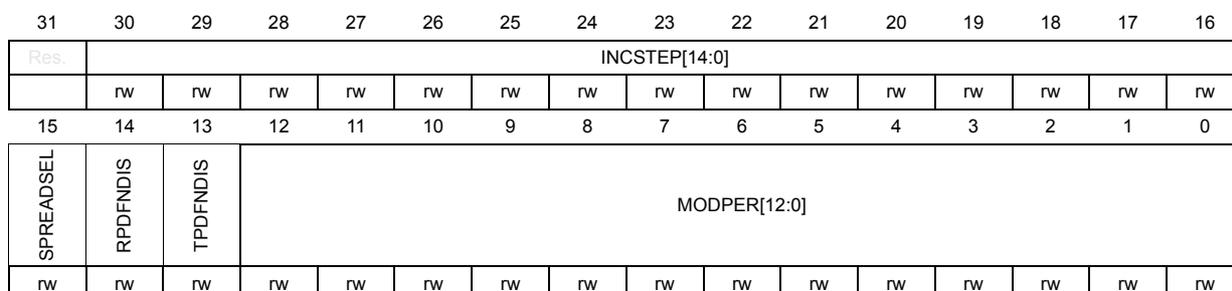
| 31 | 30 | 29 | 28 | 27 | 26 | 25 | 24 | 23 | 22 | 21 | 20 | 19 | 18 | 17 | 16 |
| Res. | INCSTEP[14:0] | ||||||||||||||
| rw | rw | rw | rw | rw | rw | rw | rw | rw | rw | rw | rw | rw | rw | rw | |
| 15 | 14 | 13 | 12 | 11 | 10 | 9 | 8 | 7 | 6 | 5 | 4 | 3 | 2 | 1 | 0 |
| SPREADSEL | RPDFNDIS | TPDFNDIS | MODPER[12:0] | ||||||||||||
| rw | rw | rw | rw | rw | rw | rw | rw | rw | rw | rw | rw | rw | rw | rw | rw |
Bit 31 Reserved, must be kept at reset value.
Bits 30:16 INCSTEP[14:0] : Modulation Depth Adjustment for PLL3
Set and reset by software to adjust the modulation depth of the clock spreading generator.
Bit 15 SPREADSEL : Spread spectrum clock generator mode for PLL3
Set and reset by software to select the clock spreading mode.
0: Center-spread modulation selected (default after reset)
1: Down-spread modulation selected
Bit 14 RPDFNDIS : Dithering RPDF noise control for PLL3
Set and reset by software.
This bit is used to enable or disable the injection of a dithering noise into the SSCG modulator. This dithering noise is generated using a rectangular probability density function.
0: Dithering noise injection enabled (default after reset)
1: Dithering noise injection disabled
Bit 13 TPDFNDIS : Dithering TPDF noise control for PLL3
Set and reset by software.
This bit is used to enable or disable the injection of a dithering noise into the SSCG modulator. This dithering noise is generated using a triangular probability density function.
0: Dithering noise injection enabled (default after reset)
1: Dithering noise injection disabled
Bits 12:0 MODPER[12:0] : Modulation Period Adjustment for PLL3
Set and reset by software to adjust the modulation period of the clock spreading generator.
7.8.24 RCC AHB peripheral kernel clock selection register (RCC_CCIPR1)
Address offset: 0x04C
Reset value: 0x0000 0A00
Changing the clock source on-the-fly is allowed (except for CKPERSEL and ETH1REFCKSEL[1:0] !) and does not generate any timing violation. However the user must make sure that both the previous and the new clock sources are present during the switching, and during the whole transition time. Refer to Clock switches and gating .
| 31 | 30 | 29 | 28 | 27 | 26 | 25 | 24 | 23 | 22 | 21 | 20 | 19 | 18 | 17 | 16 |
|---|---|---|---|---|---|---|---|---|---|---|---|---|---|---|---|
| Res. | Res. | CKPERSEL[1:0] | PSSISEL | Res. | ADCSEL[1:0] | Res. | ADF1SEL[2:0] | Res. | ETH1PHYCKSEL | ETH1REFCKSEL[1:0] | |||||
| rw | rw | rw | rw | rw | rw | rw | rw | rw | rw | rw | |||||
| 15 | 14 | 13 | 12 | 11 | 10 | 9 | 8 | 7 | 6 | 5 | 4 | 3 | 2 | 1 | 0 |
| OTGFSSSEL[1:0] | USBPHYCSEL[1:0] | USBREFCKSEL[3:0] | XSP12SEL[1:0] | XSP11SEL[1:0] | Res. | SDMMC12SEL | FMCSSEL[1:0] | ||||||||
| rw | rw | rw | rw | rw | rw | rw | rw | rw | rw | rw | rw | rw | rw | rw | |
Bits 31:30 Reserved, must be kept at reset value.
Bits 29:28 CKPERSEL[1:0] : per_ck clock source selection
- 00: hsi_ker_ck selected as per_ck clock (default after reset)
- 01: csi_ker_ck selected as per_ck clock
- 10: hse_ker_ck selected as per_ck clock
- 11: reserved, the ck_per clock is disabled
Bit 27 PSSISEL : PSSI kernel clock source selection
Set and reset by software.
- 0: pll3_r_ck selected as kernel peripheral clock (default after reset)
- 1: per_ck selected as kernel peripheral clock
Bit 26 Reserved, must be kept at reset value.
Bits 25:24 ADCSEL[1:0] : SAR ADC kernel clock source selection
Set and reset by software.
- 00: pll2_p_ck selected as kernel peripheral clock (default after reset)
- 01: pll3_r_ck selected as kernel peripheral clock
- 10: per_ck selected as kernel peripheral clock
- others: reserved, the kernel clock is disabled
Bit 23 Reserved, must be kept at reset value.
Bits 22:20 ADF1SEL[2:0] : ADF kernel clock source selection
Set and reset by software.
0: hclk1 selected as ADF kernel clock (default after reset)
1: pll2_p_ck selected as ADF kernel clock
2: pll3_p_ck selected as ADF kernel clock
3: I2S_CKIN selected as ADF kernel clock
4: csi_ker_ck selected as ADF kernel clock
5: hsi_ker_ck selected as ADF kernel clock
Note: I2S_CKIN is an external clock taken from a pin.
Bit 19 Reserved, must be kept at reset value.
Bit 18 ETH1PHYCKSEL : Clock source selection for external Ethernet PHY
Set and reset by software.
0: hse_ker_ck selected as clock source (default after reset)
1: pll3_s_ck selected clock source
Bits 17:16 ETH1REFCKSEL[1:0] : Ethernet reference clock source selection
Set and reset by software.
00: PAD ETH_RMII_REF_CLK selected as kernel peripheral clock (default after reset)
01: hse_ker_ck selected as kernel peripheral clock
10: eth_clk_fb selected as kernel peripheral clock
others: reserved, the kernel clock is disabled
Bits 15:14 OTGFSSEL[1:0] : OTGFS kernel clock source selection
Set and reset by software.
00: hsi48_ker_ck (default after reset)
01: pll3_q_ck
10: hse_ker_ck
11: clk48mohci
Bits 13:12 USBPHYCSEL[1:0] : USBPHYC kernel clock source selection
Set and reset by software.
00: hse_ker_ck (default after reset)
01: hse_ker_ck / 2
10: pll3_q_ck
11: reserved, the kernel clock is disabled
Bits 11:8 USBREFCKSEL[3:0] : USBPHYC kernel clock frequency selection
Set and reset by software.
This field is used to indicate to the USBPHYC, the frequency of the reference kernel clock provided to the USBPHYC.
0011: The kernel clock frequency provided to the USBPHYC is 16 MHz
1000: The kernel clock frequency provided to the USBPHYC is 19.2 MHz
1001: The kernel clock frequency provided to the USBPHYC is 20MHz
1010: The kernel clock frequency provided to the USBPHYC is 24 MHz (default after reset)
1110: The kernel clock frequency provided to the USBPHYC is 26 MHz
1011: The kernel clock frequency provided to the USBPHYC is 32 MHz
others: reserved
Bits 7:6 XSPI2SEL[1:0] : XSPI2 kernel clock source selection
Set and reset by software.
00: hclk5 selected as kernel peripheral clock (default after reset)
01: pll2_s_ck selected as kernel peripheral clock
1x: pll2_t_ck selected as kernel peripheral clock
Bits 5:4 XSPI1SEL[1:0] : XSPI1 kernel clock source selection
Set and reset by software.
00: hclk5 selected as kernel peripheral clock (default after reset)
01: pll2_s_ck selected as kernel peripheral clock
1x: pll2_t_ck selected as kernel peripheral clock
Bit 3 Reserved, must be kept at reset value.
Bit 2 SDMMC12SEL : SDMMC1 and SDMMC2 kernel clock source selection
Set and reset by software.
0: pll2_s_ck selected as kernel peripheral clock (default after reset)
1: pll2_t_ck selected as kernel peripheral clock
Bits 1:0 FMCSEL[1:0] : FMC kernel clock source selection
Set and reset by software.
00: hclk5 selected as kernel peripheral clock (default after reset)
01: pll1_q_ck selected as kernel peripheral clock
10: pll2_r_ck selected as kernel peripheral clock
11: hsi_ker_ck selected as kernel peripheral clock
7.8.25 RCC APB1 peripherals kernel clock selection register (RCC_CCIPR2)
Address offset: 0x050
Reset value: 0x0000 0000
Changing the clock source on-the-fly is allowed and does not generate any timing violation. However the user must make sure that both the previous and the new clock sources are present during the switching, and during the whole transition time. Refer to Clock switches and gating .
| 31 | 30 | 29 | 28 | 27 | 26 | 25 | 24 | 23 | 22 | 21 | 20 | 19 | 18 | 17 | 16 |
|---|---|---|---|---|---|---|---|---|---|---|---|---|---|---|---|
| Res. | Res. | CECSEL[1:0] | Res. | Res. | SPDIFRXSEL[1:0] | FDCANSEL[1:0] | Res. | Res. | Res. | LPTIM1SEL[2:0] | |||||
| rw | rw | rw | rw | rw | rw | rw | rw | rw | |||||||
| 15 | 14 | 13 | 12 | 11 | 10 | 9 | 8 | 7 | 6 | 5 | 4 | 3 | 2 | 1 | 0 |
| Res. | Res. | I2C1_3C1SEL[1:0] | Res. | Res. | I2C23SEL[1:0] | Res. | SPI23SEL[2:0] | Res. | UART234578SEL[2:0] | ||||||
| rw | rw | rw | rw | rw | rw | rw | rw | rw | rw | ||||||
Bits 31:30 Reserved, must be kept at reset value.
Bits 29:28 CECSEL[1:0] : HDMI-CEC kernel clock source selection
Set and reset by software.
00: lse_ck selected as kernel clock (default after reset)
01: lsi_ck selected as kernel clock
10: csi_ker_ck divided by 122 selected as kernel clock
11: reserved, the kernel clock is disabled
Bits 27:26 Reserved, must be kept at reset value.
Bits 25:24 SPDIFRXSEL[1:0] : SPDIFRX kernel clock source selection
00: pll1_q_ck selected as SPDIFRX kernel clock (default after reset)
01: pll2_r_ck selected as SPDIFRX kernel clock
10: pll3_r_ck selected as SPDIFRX kernel clock
11: hsi_ker_ck selected as SPDIFRX kernel clock
Bits 23:22 FDCANSEL[1:0] : FDCAN kernel clock source selection
00: hse_ker_ck selected as FDCAN kernel clock (default after reset)
01: pll1_q_ck selected as FDCAN kernel clock
10: pll2_p_ck selected as FDCAN kernel clock
11: reserved, the kernel clock is disabled
Bits 21:19 Reserved, must be kept at reset value.
Bits 18:16 LPTIM1SEL[2:0] : LPTIM1 kernel clock source selection
Set and reset by software.
000: pclk1 selected as kernel peripheral clock (default after reset)
001: pll2_p_ck selected as kernel peripheral clock
010: pll3_r_ck selected as kernel peripheral clock
011: lse_ck selected as kernel peripheral clock
100: lsi_ck selected as kernel peripheral clock
101: per_ck selected as kernel peripheral clock
others: reserved, the kernel clock is disabled
Bits 15:14 Reserved, must be kept at reset value.
Bits 13:12 I2C1_I3C1SEL[1:0] : I2C1 or I3C1 kernel clock source selection
Set and reset by software.
00: pclk1 selected as kernel peripheral clock (default after reset)
01: pll3_r_ck selected as kernel peripheral clock
10: hsi_ker_ck selected as kernel peripheral clock
11: csi_ker_ck selected as kernel peripheral clock
Bits 11:10 Reserved, must be kept at reset value.
Bits 9:8 I2C23SEL[1:0] : I2C2, I2C3 kernel clock source selection
Set and reset by software.
00: pclk1 selected as kernel clock (default after reset)
01: pll3_r_ck selected as kernel clock
10: hsi_ker_ck selected as kernel clock
11: csi_ker_ck selected as kernel clock
Bit 7 Reserved, must be kept at reset value.
Bits 6:4 SPI23SEL[2:0] : SPI/I2S2 and SPI/I2S3 kernel clock source selection
Set and reset by software.
Caution: If the selected clock is the external clock and this clock is stopped, it is not possible to switch to another clock. Refer to Clock switches and gating on page 412 for additional information.
000: pll1_q_ck selected as kernel clock (default after reset)
001: pll2_p_ck selected as kernel clock
010: pll3_p_ck selected as kernel clock
011: I2S_CKIN selected as kernel clock
100: per_ck selected as kernel clock
others: reserved, the kernel clock is disabled
Note: I2S_CKIN is an external clock taken from a pin.
Bit 3 Reserved, must be kept at reset value.
Bits 2:0 UART234578SEL[2:0] : USART2,3, USART4,5,7,8 (APB1) kernel clock source selection
Set and reset by software.
000: pclk1 selected as kernel clock (default after reset)
001: pll2_q_ck selected as kernel clock
010: pll3_q_ck selected as kernel clock
011: hsi_ker_ck selected as kernel clock
100: csi_ker_ck selected as kernel clock
101: lse_ck selected as kernel clock
others: reserved, the kernel clock is disabled
7.8.26 RCC APB2 peripherals kernel clock selection register (RCC_CCIPR3)
Address offset: 0x054
Reset value: 0x0000 0000
Changing the clock source on-the-fly is allowed and does not generate any timing violation. However the user must make sure that both the previous and the new clock sources are present during the switching, and during the whole transition time. Refer to Clock switches and gating .
| 31 | 30 | 29 | 28 | 27 | 26 | 25 | 24 | 23 | 22 | 21 | 20 | 19 | 18 | 17 | 16 |
|---|---|---|---|---|---|---|---|---|---|---|---|---|---|---|---|
| Res. | Res. | Res. | Res. | Res. | Res. | Res. | Res. | Res. | SAI2SEL[2:0] | Res. | SAI1SEL[2:0] | ||||
| rw | rw | rw | rw | rw | rw | ||||||||||
| 15 | 14 | 13 | 12 | 11 | 10 | 9 | 8 | 7 | 6 | 5 | 4 | 3 | 2 | 1 | 0 |
| Res. | Res. | Res. | Res. | Res. | SPI1SEL[2:0] | Res. | SPI45SEL[2:0] | Res. | USART1SEL[2:0] | ||||||
| rw | rw | rw | rw | rw | rw | rw | rw | rw | |||||||
Bits 31:23 Reserved, must be kept at reset value.
Bits 22:20 SAI2SEL[2:0] : SAI2 kernel clock source selection
Set and reset by software.
Caution: If the selected clock is the external clock and this clock is stopped, it is not possible to switch to another clock. Refer to Clock switches and gating on page 412 for additional information.
000: pll1_q_ck selected as SAI2 kernel clock (default after reset)
001: pll2_p_ck selected as SAI2 kernel clock
010: pll3_p_ck selected as SAI2 kernel clock
011: I2S_CKIN selected as SAI2 kernel clock
100: per_ck selected as SAI2 kernel clock
101: spdifrx_symb_ck selected as SAI2 kernel clock
others: reserved, the kernel clock is disabled
Note: I2S_CKIN is an external clock taken from a pin. spdifrx_symb_ck is the symbol clock generated by the spdifrx (see Figure 53).
Bit 19 Reserved, must be kept at reset value.
Bits 18:16 SAI1SEL[2:0] : SAI1 kernel clock source selection
Set and reset by software.
Caution: If the selected clock is the external clock and this clock is stopped, it is not possible to switch to another clock. Refer to Clock switches and gating on page 412 for additional information.
000: pll1_q_ck selected as SAI1 kernel clock (default after reset)
001: pll2_p_ck selected as SAI1 kernel clock
010: pll3_p_ck selected as SAI1 kernel clock
011: I2S_CKIN selected as SAI1 kernel clock
100: per_ck selected as SAI1 kernel clock
others: reserved, the kernel clock is disabled
Note: I2S_CKIN is an external clock taken from a pin.
Bits 15:11 Reserved, must be kept at reset value.
Bits 10:8 SPI1SEL[2:0] : SPI/I2S1 kernel clock source selection
Set and reset by software.
Caution: If the selected clock is the external clock and this clock is stopped, it is not possible to switch to another clock. Refer to Clock switches and gating on page 412 for additional information.
000: pll1_q_ck selected as SPI/I2S1 and 7 kernel clock (default after reset)
001: pll2_p_ck selected as SPI/I2S1 and 7 kernel clock
010: pll3_p_ck selected as SPI/I2S1 and 7 kernel clock
011: I2S_CKIN selected as SPI/I2S1 and 7 kernel clock
100: per_ck selected as SPI/I2S1, and 7 kernel clock
others: reserved, the kernel clock is disabled
Note: I2S_CKIN is an external clock taken from a pin.
Bit 7 Reserved, must be kept at reset value.
Bits 6:4 SPI45SEL[2:0] : SPI4 and 5 kernel clock source selection
Set and reset by software.
000: pclk2 selected as kernel clock (default after reset)
001: pll2_q_ck is selected as kernel clock
010: pll3_q_ck is selected as kernel clock
011: hsi_ker_ck is selected as kernel clock
100: csi_ker_ck is selected as kernel clock
101: hse_ker_ck is selected as kernel clock
others: reserved, the kernel clock is disabled
Bit 3 Reserved, must be kept at reset value.
Bits 2:0 USART1SEL[2:0] : USART1 kernel clock source selection
Set and reset by software.
000: pclk2 selected as kernel clock (default after reset)
001: pll2_q_ck selected as kernel clock
010: pll3_q_ck selected as kernel clock
011: hsi_ker_ck selected as kernel clock
100: csi_ker_ck selected as kernel clock
101: lse_ck selected as kernel clock
others: reserved, the kernel clock is disabled
7.8.27 RCC APB4,5 peripherals kernel clock selection register (RCC_CCIPR4)
Address offset: 0x058
Reset value: 0x0000 0000
Changing the clock source on-the-fly is allowed and does not generate any timing violation. However the user must make sure that both the previous and the new clock sources are present during the switching, and during the whole transition time. Refer to Clock switches and gating .
| 31 | 30 | 29 | 28 | 27 | 26 | 25 | 24 | 23 | 22 | 21 | 20 | 19 | 18 | 17 | 16 |
|---|---|---|---|---|---|---|---|---|---|---|---|---|---|---|---|
| Res. | Res. | Res. | Res. | Res. | Res. | Res. | Res. | Res. | Res. | Res. | Res. | Res. | Res. | Res. | Res. |
| 15 | 14 | 13 | 12 | 11 | 10 | 9 | 8 | 7 | 6 | 5 | 4 | 3 | 2 | 1 | 0 |
| Res. | LPTIM45SEL[2:0] | Res. | LPTIM23SEL[2:0] | Res. | SPI6SEL[2:0] | Res. | LPUART1SEL[2:0] | ||||||||
| rw | rw | rw | rw | rw | rw | rw | rw | rw | rw | rw | rw | ||||
Bits 31:15 Reserved, must be kept at reset value.
Bits 14:12 LPTIM45SEL[2:0] : LPTIM4, and LPTIM5 kernel clock source selection
Set and reset by software.
000: pclk4 selected as kernel peripheral clock (default after reset)
001: pll2_p_ck selected as kernel peripheral clock
010: pll3_r_ck selected as kernel peripheral clock
011: lse_ck selected as kernel peripheral clock
100: lsi_ck selected as kernel peripheral clock
101: per_ck selected as kernel peripheral clock
others: reserved, the kernel clock is disabled
Bit 11 Reserved, must be kept at reset value.
Bits 10:8 LPTIM23SEL[2:0] : LPTIM2 and LPTIM3 kernel clock source selection
Set and reset by software.
000: pclk4 selected as kernel peripheral clock (default after reset)
001: pll2_p_ck selected as kernel peripheral clock
010: pll3_r_ck selected as kernel peripheral clock
011: lse_ck selected as kernel peripheral clock
100: lsi_ck selected as kernel peripheral clock
101: per_ck selected as kernel peripheral clock
others: reserved, the kernel clock is disabled
Bit 7 Reserved, must be kept at reset value.
Bits 6:4 SPI6SEL[2:0] : SPI/I2S6 kernel clock source selection
Set and reset by software.
000: pclk4 selected as kernel peripheral clock (default after reset)
001: pll2_q_ck selected as kernel peripheral clock
010: pll3_q_ck selected as kernel peripheral clock
011: hsi_ker_ck selected as kernel peripheral clock
100: csi_ker_ck selected as kernel peripheral clock
101: hse_ker_ck selected as kernel peripheral clock
others: reserved, the kernel clock is disabled
Bit 3 Reserved, must be kept at reset value.
Bits 2:0 LPUART1SEL[2:0] : LPUART1 kernel clock source selection
Set and reset by software.
000: pclk4 selected as kernel peripheral clock (default after reset)
001: pll2_q_ck selected as kernel peripheral clock
010: pll3_q_ck selected as kernel peripheral clock
011: hsi_ker_ck selected as kernel peripheral clock
100: csi_ker_ck selected as kernel peripheral clock
101: lse_ck selected as kernel peripheral clock
others: reserved, the kernel clock is disabled
7.8.28 RCC clock source interrupt enable register (RCC_CIER)
Address offset: 0x060
Reset value: 0x0000 0000
| 31 | 30 | 29 | 28 | 27 | 26 | 25 | 24 | 23 | 22 | 21 | 20 | 19 | 18 | 17 | 16 |
|---|---|---|---|---|---|---|---|---|---|---|---|---|---|---|---|
| Res. | Res. | Res. | Res. | Res. | Res. | Res. | Res. | Res. | Res. | Res. | Res. | Res. | Res. | Res. | Res. |
| 15 | 14 | 13 | 12 | 11 | 10 | 9 | 8 | 7 | 6 | 5 | 4 | 3 | 2 | 1 | 0 |
| Res. | Res. | Res. | Res. | Res. | Res. | LSECSSIE | PLL3RDYIE | PLL2RDYIE | PLL1RDYIE | HSI48RDYIE | CSIRDYIE | HSERDYIE | HSIRDYIE | LSERDYIE | LSIRDYIE |
| rw | rw | rw | rw | rw | rw | rw | rw | rw | rw |
Bits 31:10 Reserved, must be kept at reset value.
Bit 9 LSECSSIE : LSE clock security system interrupt enable
Set and reset by software to enable/disable interrupt caused by the clock security system (CSS) on external 32 kHz oscillator.
0: LSE CSS interrupt disabled (default after reset)
1: LSE CSS interrupt enabled
Bit 8 PLL3RDYIE : PLL3 ready interrupt enable
Set and reset by software to enable/disable interrupt caused by PLL3 lock.
0: PLL3 lock interrupt disabled (default after reset)
1: PLL3 lock interrupt enabled
Bit 7 PLL2RDYIE : PLL2 ready interrupt enable
Set and reset by software to enable/disable interrupt caused by PLL2 lock.
0: PLL2 lock interrupt disabled (default after reset)
1: PLL2 lock interrupt enabled
Bit 6 PLL1RDYIE : PLL1 ready interrupt enable
Set and reset by software to enable/disable interrupt caused by PLL1 lock.
0: PLL1 lock interrupt disabled (default after reset)
1: PLL1 lock interrupt enabled
Bit 5 HSI48RDYIE : HSI48 ready interrupt enable
Set and reset by software to enable/disable interrupt caused by the HSI48 oscillator stabilization.
0: HSI48 ready interrupt disabled (default after reset)
1: HSI48 ready interrupt enabled
Bit 4 CSIRDYIE : CSI ready interrupt enable
Set and reset by software to enable/disable interrupt caused by the CSI oscillator stabilization.
0: CSI ready interrupt disabled (default after reset)
1: CSI ready interrupt enabled
Bit 3 HSERDYIE : HSE ready interrupt enable
Set and reset by software to enable/disable interrupt caused by the HSE oscillator stabilization.
0: HSE ready interrupt disabled (default after reset)
1: HSE ready interrupt enabled
Bit 2 HSIRDYIE : HSI ready interrupt enable
Set and reset by software to enable/disable interrupt caused by the HSI oscillator stabilization.
0: HSI ready interrupt disabled (default after reset)
1: HSI ready interrupt enabled
Bit 1 LSERDYIE : LSE ready interrupt enable
Set and reset by software to enable/disable interrupt caused by the LSE oscillator stabilization.
0: LSE ready interrupt disabled (default after reset)
1: LSE ready interrupt enabled
Bit 0 LSIRDYIE : LSI ready interrupt enable
Set and reset by software to enable/disable interrupt caused by the LSI oscillator stabilization.
0: LSI ready interrupt disabled (default after reset)
1: LSI ready interrupt enabled
7.8.29 RCC clock source interrupt flag register (RCC_CIFR)
Address offset: 0x64
Reset value: 0x0000 0000
| 31 | 30 | 29 | 28 | 27 | 26 | 25 | 24 | 23 | 22 | 21 | 20 | 19 | 18 | 17 | 16 |
|---|---|---|---|---|---|---|---|---|---|---|---|---|---|---|---|
| Res. | Res. | Res. | Res. | Res. | Res. | Res. | Res. | Res. | Res. | Res. | Res. | Res. | Res. | Res. | Res. |
| 15 | 14 | 13 | 12 | 11 | 10 | 9 | 8 | 7 | 6 | 5 | 4 | 3 | 2 | 1 | 0 |
| Res. | Res. | Res. | Res. | Res. | HSECSSF | LSECSSF | PLL3RDYF | PLL2RDYF | PLL1RDYF | HSI48RDYF | CSIRDYF | HSERDYF | HSIRDYF | LSERDYF | LSIRDYF |
| r | r | r | r | r | r | r | r | r | r | r |
Bits 31:11 Reserved, must be kept at reset value.
Bit 10 HSECSSF : HSE clock security system interrupt flag
Reset by software by writing HSECSSC bit.
Set by hardware in case of HSE clock failure.
0: no clock security interrupt caused by HSE clock failure (default after reset)
1: clock security interrupt caused by HSE clock failure
Bit 9 LSECSSF : LSE clock security system interrupt flag
Reset by software by writing LSECSSC bit.
Set by hardware when a failure is detected on the external 32 kHz oscillator and LSECSSIE is set.
0: no failure detected on the external 32 kHz oscillator (default after reset)
1: failure detected on the external 32 kHz oscillator
Bit 8 PLL3RDYF : PLL3 ready interrupt flag
Reset by software by writing PLL3RDYC bit.
Set by hardware when the PLL3 locks and PLL3RDYIE is set.
0: no clock ready interrupt caused by PLL3 lock (default after reset)
1: clock ready interrupt caused by PLL3 lock
Bit 7 PLL2RDYF: PLL2 ready interrupt flagReset by software by writing PLL2RDYC bit.
Set by hardware when the PLL2 locks and PLL2RDYIE is set.
0: no clock ready interrupt caused by PLL2 lock (default after reset)
1: clock ready interrupt caused by PLL2 lock
Bit 6 PLL1RDYF: PLL1 ready interrupt flagReset by software by writing PLL1RDYC bit.
Set by hardware when the PLL1 locks and PLL1RDYIE is set.
0: no clock ready interrupt caused by PLL1 lock (default after reset)
1: clock ready interrupt caused by PLL1 lock
Bit 5 HSI48RDYF: HSI48 ready interrupt flagReset by software by writing HSI48RDYC bit.
Set by hardware when the HSI48 clock becomes stable and HSI48RDYIE is set.
0: no clock ready interrupt caused by the HSI48 oscillator (default after reset)
1: clock ready interrupt caused by the HSI48 oscillator
Bit 4 CSIRDYF: CSI ready interrupt flagReset by software by writing CSIRDYC bit.
Set by hardware when the CSI clock becomes stable and CSIRDYIE is set.
0: no clock ready interrupt caused by the CSI (default after reset)
1: clock ready interrupt caused by the CSI
Bit 3 HSERDYF: HSE ready interrupt flagReset by software by writing HSERDYC bit.
Set by hardware when the HSE clock becomes stable and HSERDYIE is set.
0: no clock ready interrupt caused by the HSE (default after reset)
1: clock ready interrupt caused by the HSE
Bit 2 HSIRDYF: HSI ready interrupt flagReset by software by writing HSIRDYC bit.
Set by hardware when the HSI clock becomes stable and HSIRDYIE is set.
0: no clock ready interrupt caused by the HSI (default after reset)
1: clock ready interrupt caused by the HSI
Bit 1 LSERDYF: LSE ready interrupt flagReset by software by writing LSERDYC bit.
Set by hardware when the LSE clock becomes stable and LSERDYIE is set.
0: no clock ready interrupt caused by the LSE (default after reset)
1: clock ready interrupt caused by the LSE
Bit 0 LSIRDYF: LSI ready interrupt flagReset by software by writing LSIRDYC bit.
Set by hardware when the LSI clock becomes stable and LSIRDYIE is set.
0: no clock ready interrupt caused by the LSI (default after reset)
1: clock ready interrupt caused by the LSI
7.8.30 RCC clock source interrupt clear register (RCC_CICR)
Address offset: 0x68
Reset value: 0x0000 0000
| 31 | 30 | 29 | 28 | 27 | 26 | 25 | 24 | 23 | 22 | 21 | 20 | 19 | 18 | 17 | 16 |
|---|---|---|---|---|---|---|---|---|---|---|---|---|---|---|---|
| Res. | Res. | Res. | Res. | Res. | Res. | Res. | Res. | Res. | Res. | Res. | Res. | Res. | Res. | Res. | Res. |
| 15 | 14 | 13 | 12 | 11 | 10 | 9 | 8 | 7 | 6 | 5 | 4 | 3 | 2 | 1 | 0 |
| Res. | Res. | Res. | Res. | Res. | HSECSSC | LSECSSC | PLL3RDYC | PLL2RDYC | PLL1RDYC | HSI48RDYC | CSIIRDYC | HSERDYC | HSIRDYC | LSERDYC | LSIRDYC |
| rc_w1 | rc_w1 | rc_w1 | rc_w1 | rc_w1 | rc_w1 | rc_w1 | rc_w1 | rc_w1 | rc_w1 | rc_w1 |
Bits 31:11 Reserved, must be kept at reset value.
Bit 10 HSECSSC : HSE clock security system interrupt clear
Set by software to clear HSECSSF.
Reset by hardware when clear done.
0: HSECSSF no effect (default after reset)
1: HSECSSF cleared
Bit 9 LSECSSC : LSE clock security system interrupt clear
Set by software to clear LSECSSF.
Reset by hardware when clear done.
0: LSECSSF no effect (default after reset)
1: LSECSSF cleared
Bit 8 PLL3RDYC : PLL3 ready interrupt clear
Set by software to clear PLL3RDYF.
Reset by hardware when clear done.
0: PLL3RDYF no effect (default after reset)
1: PLL3RDYF cleared
Bit 7 PLL2RDYC : PLL2 ready interrupt clear
Set by software to clear PLL2RDYF.
Reset by hardware when clear done.
0: PLL2RDYF no effect (default after reset)
1: PLL2RDYF cleared
Bit 6 PLL1RDYC : PLL1 ready interrupt clear
Set by software to clear PLL1RDYF.
Reset by hardware when clear done.
0: PLL1RDYF no effect (default after reset)
1: PLL1RDYF cleared
Bit 5 HSI48RDYC : HSI48 ready interrupt clear
Set by software to clear HSI48RDYF.
Reset by hardware when clear done.
0: HSI48RDYF no effect (default after reset)
1: HSI48RDYF cleared
- Bit 4
CSIRDYC
: CSI ready interrupt clear
Set by software to clear CSIRDYF.
Reset by hardware when clear done.
0: CSIRDYF no effect (default after reset)
1: CSIRDYF cleared - Bit 3
HSERDYC
: HSE ready interrupt clear
Set by software to clear HSERDYF.
Reset by hardware when clear done.
0: HSERDYF no effect (default after reset)
1: HSERDYF cleared - Bit 2
HSIRDYC
: HSI ready interrupt clear
Set by software to clear HSIRDYF.
Reset by hardware when clear done.
0: HSIRDYF no effect (default after reset)
1: HSIRDYF cleared - Bit 1
LSERDYC
: LSE ready interrupt clear
Set by software to clear LSERDYF.
Reset by hardware when clear done.
0: LSERDYF no effect (default after reset)
1: LSERDYF cleared - Bit 0
LSIRDYC
: LSI ready interrupt clear
Set by software to clear LSIRDYF.
Reset by hardware when clear done.
0: LSIRDYF no effect (default after reset)
1: LSIRDYF cleared
7.8.31 RCC Backup domain control register (RCC_BDCR)
Address offset: 0x070
Reset value: 0x0000 0010
Reset by Backup domain reset.
Access: 4 wait states (resynchronization) are inserted in case of successive accesses to this register.
After a system reset, the RCC_BDCR register is write-protected. To modify this register, the DBP bit in the PWR control register 1 (PWR_CR1) must be set to 1. RCC_BDCR bits are only reset after a Backup domain reset (see Section 7.4.5: Backup domain reset ). Any other internal or external reset does not have any effect on these bits.
| 31 | 30 | 29 | 28 | 27 | 26 | 25 | 24 | 23 | 22 | 21 | 20 | 19 | 18 | 17 | 16 |
|---|---|---|---|---|---|---|---|---|---|---|---|---|---|---|---|
| Res. | Res. | Res. | Res. | Res. | Res. | Res. | Res. | Res. | Res. | Res. | Res. | Res. | Res. | Res. | VSWRST |
| rw | |||||||||||||||
| 15 | 14 | 13 | 12 | 11 | 10 | 9 | 8 | 7 | 6 | 5 | 4 | 3 | 2 | 1 | 0 |
| RTCEN | Res. | Res. | LSECSSRA | Res. | Res. | RTCSEL[1:0] | LSEEXT | LSECSSD | LSECSSON | LSEDRV[1:0] | LSEBYP | LSERDY | LSEON | ||
| rw | rw | rwo | rwo | rw | r | rs | rw | rw | rw | r | rw | ||||
Bits 31:17 Reserved, must be kept at reset value.
Bit 16 VSWRST : VSwitch domain software reset
Set and reset by software.
To generate a VSW reset, it is recommended to write this bit to 1, then back to 0.
0: reset not activated (default after Backup domain reset)
1: generates a reset pulse, resetting the entire VSW domain.
Bit 15 RTCEN : RTC clock enable
Set and reset by software.
0: rtc_ck disabled (default after Backup domain reset)
1: rtc_ck enabled
Bits 14:13 Reserved, must be kept at reset value.
Bit 12 LSECSSRA : Re-Arm the LSECSS function
Set by software.
After a LSE failure detection, the software application can re-enable the LSECSS by writing this bit to 1. Reading this bit returns the written value. Prior to set this bit to 1, LSECSSON must be set to 0.
Refer to Section : CSS on LSE for details.
0: Writing 0 has no effect (default after Backup domain reset)
1: Writing 1 generates a re-arm pulse for the LSECSS function
Bits 11:10 Reserved, must be kept at reset value.
Bits 9:8 RTCSEL[1:0]: RTC clock source selectionSet by software to select the clock source for the RTC. These bits can be written only one time (except in case of failure detection on LSE). These bits must be written before LSECSSON is enabled. The VSWRST bit can be used to reset them, then it can be written one time again.
If HSE is selected as RTC clock, this clock is lost when the system is in Stop mode or in case of a pin reset (NRST).
00: no clock (default after Backup domain reset)
01: LSE selected as RTC clock
10: LSI selected as RTC clock
11: HSE divided by RTCPRE value selected as RTC clock
Bit 7 LSEEXT: low-speed external clock type in Bypass modeSet and reset by software to select the external clock type (analog or digital).
The external clock must be enabled with the LSEON bit, to be used by the device.
The LSEEXT bit can be written only if the LSE oscillator is disabled.
0: LSE in analog mode (default after Backup domain reset)
1: LSE in digital mode (do not use if RTC is active).
Bit 6 LSECSSD: LSE clock security system failure detectionSet by hardware to indicate when a failure has been detected by the clock security system on the external 32 kHz oscillator.
0: no failure detected on 32 kHz oscillator (default after Backup domain reset)
1: failure detected on 32 kHz oscillator
Bit 5 LSECSSON: LSE clock security system enableSet by software to enable the clock security system on 32 kHz oscillator.
LSECSSON must be enabled after LSE is enabled (LSEON enabled) and ready (LSERDY set by hardware) and after RTCSEL is selected.
Once enabled, this bit can only be disabled,
- – After a LSE failure detection (LSECSSD = 1). In that case the software must disable LSECSSON.
- – After a back-up domain reset
0: CSS on 32 kHz oscillator OFF (default after Backup domain reset)
1: CSS on 32 kHz oscillator ON
Bits 4:3 LSEDRV[1:0]: LSE oscillator driving capabilitySet by software to select the driving capability of the LSE oscillator.
00: lowest drive
01: medium-low drive
10: medium-high drive (default after backup domain if LSEON=0)
11: highest drive
Bit 2 LSEBYP : LSE oscillator bypass
Set and reset by software to bypass oscillator in debug mode. This bit must not be written when the LSE is enabled (by LSEON) or ready (LSERDY = 1)
0: LSE oscillator not bypassed (default after Backup domain reset)
1: LSE oscillator bypassed
Bit 1 LSERDY : LSE oscillator ready
Set and reset by hardware to indicate when the LSE is stable. This bit needs 6 cycles of lse_ck clock to fall down after LSEON has been set to 0.
0: LSE oscillator not ready (default after Backup domain reset)
1: LSE oscillator ready
Bit 0 LSEON : LSE oscillator enabled
Set and reset by software.
0: LSE oscillator OFF (default after Backup domain reset)
1: LSE oscillator ON
7.8.32 RCC clock control and status register (RCC_CSR)
Address offset: 0x074
Reset value: 0x0000 0000
Access: 4 wait states (resynchronization) are inserted are inserted in case of successive accesses to this register.
| 31 | 30 | 29 | 28 | 27 | 26 | 25 | 24 | 23 | 22 | 21 | 20 | 19 | 18 | 17 | 16 |
|---|---|---|---|---|---|---|---|---|---|---|---|---|---|---|---|
| Res. | Res. | Res. | Res. | Res. | Res. | Res. | Res. | Res. | Res. | Res. | Res. | Res. | Res. | Res. | Res. |
| 15 | 14 | 13 | 12 | 11 | 10 | 9 | 8 | 7 | 6 | 5 | 4 | 3 | 2 | 1 | 0 |
| Res. | Res. | Res. | Res. | Res. | Res. | Res. | Res. | Res. | Res. | Res. | Res. | Res. | Res. | LSIRDY | LSION |
| r | rw |
Bits 31:2 Reserved, must be kept at reset value.
Bit 1 LSIRDY : LSI oscillator ready
Set and reset by hardware to indicate when the low-speed internal RC oscillator is stable.
This bit needs 3 cycles of lsi_ck clock to fall down after LSION has been set to 0.
This bit can be set even when LSION is not enabled if there is a request for LSI clock by the clock security system on LSE or by the low-speed watchdog or by the RTC.
0: LSI clock is not ready (default after reset)
1: LSI clock is ready
Bit 0 LSION : LSI oscillator enable
Set and reset by software.
0: LSI is OFF (default after reset)
1: LSI is ON
7.8.33 RCC AHB1 peripheral reset register (RCC_AHB1RSTR)
Address offset: 0x080
Reset value: 0x0000 0000
| 31 | 30 | 29 | 28 | 27 | 26 | 25 | 24 | 23 | 22 | 21 | 20 | 19 | 18 | 17 | 16 |
|---|---|---|---|---|---|---|---|---|---|---|---|---|---|---|---|
| ADF1RST | Res. | Res. | Res. | OTGFSRST | USBPHYCRST | OTGHSRST | Res. | Res. | Res. | Res. | Res. | Res. | Res. | Res. | Res. |
| r/w | r/w | r/w | r/w |
| 15 | 14 | 13 | 12 | 11 | 10 | 9 | 8 | 7 | 6 | 5 | 4 | 3 | 2 | 1 | 0 |
|---|---|---|---|---|---|---|---|---|---|---|---|---|---|---|---|
| ETH1RST | Res. | Res. | Res. | Res. | Res. | Res. | Res. | Res. | Res. | ADC12RST | GPDMA1RST | Res. | Res. | Res. | Res. |
| r/w | r/w | r/w |
Bit 31 ADF1RST : ADF block reset
Set and reset by software.
0: does not reset ADF block (default after reset)
1: resets ADF block
Bits 30:28 Reserved, must be kept at reset value.
Bit 27 OTGFSRST : OTGFS block reset
Set and reset by software.
0: does not reset OTGFS block (default after reset)
1: resets OTGFS block
Bit 26 USBPHYCRST : USBPHYC block reset
Set and reset by software.
0: does not reset USBPHYC block (default after reset)
1: resets USBPHYC block
Bit 25 OTGHSRST : OTGHS block reset
Set and reset by software.
0: does not reset OTGHS block (default after reset)
1: resets OTGHS block
Bits 24:16 Reserved, must be kept at reset value.
Bit 15 ETH1RST : ETH1 block reset
Set and reset by software.
0: does not reset ETH1 block (default after reset)
1: resets ETH1 block
Bits 14:6 Reserved, must be kept at reset value.
Bit 5 ADC12RST : ADC1 and 2 blocks reset
Set and reset by software.
0: does not reset ADC1 and 2 blocks (default after reset)
1: resets ADC1 and 2 blocks
Bit 4 GPDMA1RST : GPDMA1 blocks reset
Set and reset by software.
0: does not reset GPDMA1 block (default after reset)
1: resets GPDMA1 block
Bits 3:0 Reserved, must be kept at reset value.
7.8.34 RCC AHB2 peripheral reset register (RCC_AHB2RSTR)
Address offset: 0x084
Reset value: 0x0000 0000
| 31 | 30 | 29 | 28 | 27 | 26 | 25 | 24 | 23 | 22 | 21 | 20 | 19 | 18 | 17 | 16 |
|---|---|---|---|---|---|---|---|---|---|---|---|---|---|---|---|
| Res. | Res. | Res. | Res. | Res. | Res. | Res. | Res. | Res. | Res. | Res. | Res. | Res. | Res. | Res. | Res. |
| 15 | 14 | 13 | 12 | 11 | 10 | 9 | 8 | 7 | 6 | 5 | 4 | 3 | 2 | 1 | 0 |
| Res. | CORDICRST | Res. | Res. | Res. | Res. | SDMMC2RST | Res. | Res. | Res. | Res. | Res. | Res. | Res. | PSSIRST | Res. |
| rw | rw | rw |
Bits 31:15 Reserved, must be kept at reset value.
Bit 14 CORDICRST : CORDIC reset
Set and reset by software.
0: does not reset CORDIC block (default after reset)
1: resets CORDIC block
Bits 13:10 Reserved, must be kept at reset value.
Bit 9 SDMMC2RST : SDMMC2 and SDMMC2 delay blocks reset
Set and reset by software.
0: does not reset SDMMC2 and SDMMC2 delay blocks (default after reset)
1: resets SDMMC2 and SDMMC2 delay blocks
Bits 8:2 Reserved, must be kept at reset value.
Bit 1 PSSIRST : PSSI block reset
Set and reset by software.
0: does not reset PSSI block (default after reset)
1: resets PSSI block
Bit 0 Reserved, must be kept at reset value.
7.8.35 RCC AHB3 peripheral reset register (RCC_AHB3RSTR)
Address offset: 0x0A4
Reset value: 0x0000 0000
| 31 | 30 | 29 | 28 | 27 | 26 | 25 | 24 | 23 | 22 | 21 | 20 | 19 | 18 | 17 | 16 |
|---|---|---|---|---|---|---|---|---|---|---|---|---|---|---|---|
| Res. | Res. | Res. | Res. | Res. | Res. | Res. | Res. | Res. | Res. | Res. | Res. | Res. | Res. | Res. | Res. |
| 15 | 14 | 13 | 12 | 11 | 10 | 9 | 8 | 7 | 6 | 5 | 4 | 3 | 2 | 1 | 0 |
| Res. | Res. | Res. | Res. | Res. | Res. | Res. | Res. | Res. | PKARST | Res. | SAESRST | Res. | CRYPRST | HASHRST | RNGRST |
| rw | rw | rw | rw | rw |
Bits 31:7 Reserved, must be kept at reset value.
Bit 6 PKARST : PKA block reset
Set and reset by software.
0: does not reset PKA block (default after reset)
1: resets PKA block
Bit 5 Reserved, must be kept at reset value.
Bit 4 SAESRST : SAES block reset
Set and reset by software.
0: does not reset SAES block (default after reset)
1: resets SAES block
Bit 3 Reserved, must be kept at reset value.
Bit 2 CRYPRST : CRYP block reset
Set and reset by software.
0: does not reset CRYP block (default after reset)
1: resets CRYP block
Bit 1 HASHRST : HASH block reset
Set and reset by software.
0: does not reset HASH block (default after reset)
1: resets HASH block
Bit 0 RNGRST : random number generator block reset
Set and reset by software.
0: does not reset RNG block (default after reset)
1: resets RNG block
7.8.36 RCC AHB4 peripheral reset register (RCC_AHB4RSTR)
Address offset: 0x088
Reset value: 0x0000 0000
| 31 | 30 | 29 | 28 | 27 | 26 | 25 | 24 | 23 | 22 | 21 | 20 | 19 | 18 | 17 | 16 |
|---|---|---|---|---|---|---|---|---|---|---|---|---|---|---|---|
| Res. | Res. | Res. | Res. | Res. | Res. | Res. | Res. | Res. | Res. | Res. | Res. | CRCRST | Res. | Res. | Res. |
| 15 | 14 | 13 | 12 | 11 | 10 | 9 | 8 | 7 | 6 | 5 | 4 | 3 | 2 | 1 | 0 |
| GPIOFRST | GPIOORST | GPIONRST | GPIOIRST | Res. | Res. | Res. | Res. | GPIOHRST | GPIOGRST | GPIOFRST | GPIOERST | GPIODRST | GPIOCRST | GPIOBRST | GPIOARST |
| nw | nw | nw | nw | nw | nw | nw | nw | nw | nw | nw | nw |
Bits 31:20 Reserved, must be kept at reset value.
Bit 19 CRCRST : CRC block reset
Set and reset by software.
0: does not reset the CRC block (default after reset)
1: resets the CRC block
Bits 18:16 Reserved, must be kept at reset value.
Bit 15 GPIOFRST : GPIOF block reset
Set and reset by software.
0: does not reset the GPIOF block (default after reset)
1: resets the GPIOF block
Bit 14 GPIOORST : GPIOO block reset
Set and reset by software.
0: does not reset the GPIOO block (default after reset)
1: resets the GPIOO block
Bit 13 GPIONRST : GPION block reset
Set and reset by software.
0: does not reset the GPION block (default after reset)
1: resets the GPION block
Bit 12 GPIOIRST : GPIOI block reset
Set and reset by software.
0: does not reset the GPIOI block (default after reset)
1: resets the GPIOI block
Bits 11:8 Reserved, must be kept at reset value.
Bit 7 GPIOHRST : GPIOH block reset
Set and reset by software.
0: does not reset the GPIOH block (default after reset)
1: resets the GPIOH block
- Bit 6
GPIOGRST
: GPIOG block reset
Set and reset by software.
0: does not reset the GPIOG block (default after reset)
1: resets the GPIOG block - Bit 5
GPIOFRST
: GPIOF block reset
Set and reset by software.
0: does not reset the GPIOF block (default after reset)
1: resets the GPIOF block - Bit 4
GPIOERST
: GPIOE block reset
Set and reset by software.
0: does not reset the GPIOE block (default after reset)
1: resets the GPIOE block - Bit 3
GPIODRST
: GPIOD block reset
Set and reset by software.
0: does not reset the GPIOD block (default after reset)
1: resets the GPIOD block - Bit 2
GPIOCRST
: GPIOC block reset
Set and reset by software.
0: does not reset the GPIOC block (default after reset)
1: resets the GPIOC block - Bit 1
GPIOBRST
: GPIOB block reset
Set and reset by software.
0: does not reset the GPIOB block (default after reset)
1: resets the GPIOB block - Bit 0
GPIOARST
: GPIOA block reset
Set and reset by software.
0: does not reset the GPIOA block (default after reset)
1: resets the GPIOA block
7.8.37 RCC AHB5 peripheral reset register (RCC_AHB5RSTR)
Address offset: 0x07C
Reset value: 0x0000 0000
| 31 | 30 | 29 | 28 | 27 | 26 | 25 | 24 | 23 | 22 | 21 | 20 | 19 | 18 | 17 | 16 |
|---|---|---|---|---|---|---|---|---|---|---|---|---|---|---|---|
| Res. | Res. | Res. | Res. | Res. | Res. | Res. | Res. | Res. | Res. | Res. | GPU2DRST | GFXMMURST | Res. | Res. | Res. |
| 15 | 14 | 13 | 12 | 11 | 10 | 9 | 8 | 7 | 6 | 5 | 4 | 3 | 2 | 1 | 0 |
| Res. | XSPIMRST | Res. | XSPI2RST | Res. | Res. | Res. | SDMMC1RST | Res. | Res. | XSPI1RST | FMCRST | JPEGRST | Res. | DMA2DRST | HPDMA1RST |
| rw | rw | rw | rw | rw | rw | rw | rw |
Bits 31:21 Reserved, must be kept at reset value.
Bit 20 GPU2DRST : GPU2D block reset
Set and reset by software.
0: reset is released (default after reset)
1: reset is asserted
Bit 19 GFXMMURST : GFXMMU block reset
Set and reset by software.
0: reset is released (default after reset)
1: reset is asserted
Bits 18:15 Reserved, must be kept at reset value.
Bit 14 XSPIMRST : XSPIM reset
Set and reset by software.
0: reset is released (default after reset)
1: reset is asserted
Bit 13 Reserved, must be kept at reset value.
Bit 12 XSPI2RST : XSPI2 and MCE2 blocks reset
Set and reset by software.
The hardware prevents writing this bit if XSPICKP = 1.
0: reset is released (default after reset)
1: reset is asserted
Bits 11:9 Reserved, must be kept at reset value.
Bit 8 SDMMC1RST : SDMMC1 and DB_SDMMC1 blocks reset
Set and reset by software.
0: reset is released (default after reset)
1: reset is asserted
Bits 7:6 Reserved, must be kept at reset value.
- Bit 5
XSPI1RST
: XSPI1 and MCE1 blocks reset
Set and reset by software.
The hardware prevents writing this bit if XSPICKP = 1.
0: reset is released (default after reset)
1: reset is asserted - Bit 4
FMCRST
: FMC and MCE3 blocks reset
Set and reset by software.
The hardware prevents writing this bit if FMCCPK = 1.
0: reset is released (default after reset)
1: reset is asserted - Bit 3
JPEGRST
: JPEG block reset
Set and reset by software.
0: reset is released (default after reset)
1: reset is asserted - Bit 2 Reserved, must be kept at reset value.
- Bit 1
DMA2DRST
: DMA2D block reset
Set and reset by software.
0: reset is released (default after reset)
1: reset is asserted - Bit 0
HPDMA1RST
: HPDMA1 block reset
Set and reset by software.
0: reset is released (default after reset)
1: reset is asserted
7.8.38 RCC APB1 peripheral reset register 1 (RCC_APB1RSTR1)
Address offset: 0x090
Reset value: 0x0000 0000
| 31 | 30 | 29 | 28 | 27 | 26 | 25 | 24 | 23 | 22 | 21 | 20 | 19 | 18 | 17 | 16 |
|---|---|---|---|---|---|---|---|---|---|---|---|---|---|---|---|
| UART8RST | UART7RST | Res. | Res. | CECRST | Res. | Res. | Res. | I2C3RST | I2C2RST | I2C1_I3C1RST | UART5RST | UART4RST | USART3RST | USART2RST | SPDIFRXRST |
| r w | r w | r w | r w | r w | r w | r w | r w | r w | r w | r w |
| 15 | 14 | 13 | 12 | 11 | 10 | 9 | 8 | 7 | 6 | 5 | 4 | 3 | 2 | 1 | 0 |
|---|---|---|---|---|---|---|---|---|---|---|---|---|---|---|---|
| SPI3RST | SPI2RST | Res. | Res. | Res. | Res. | LPTIM1RST | TIM14RST | TIM13RST | TIM12RST | TIM7RST | TIM6RST | TIM5RST | TIM4RST | TIM3RST | TIM2RST |
| r w | r w | r w | r w | r w | r w | r w | r w | r w | r w | r w | r w |
Bit 31 UART8RST : UART8 block reset
Set and reset by software.
0: does not reset the UART8 block (default after reset)
1: resets the UART8 block
Bit 30 UART7RST : UART7 block reset
Set and reset by software.
0: does not reset the UART7 block (default after reset)
1: resets the UART7 block
Bits 29:28 Reserved, must be kept at reset value.
Bit 27 CECRST : HDMI-CEC block reset
Set and reset by software.
0: does not reset the HDMI-CEC block (default after reset)
1: resets the HDMI-CEC block
Bits 26:24 Reserved, must be kept at reset value.
Bit 23 I2C3RST : I2C3 block reset
Set and reset by software.
0: does not reset the I2C3 block (default after reset)
1: resets the I2C3 block
Bit 22 I2C2RST : I2C2 block reset
Set and reset by software.
0: does not reset the I2C2 block (default after reset)
1: resets the I2C2 block
Bit 21 I2C1_I3C1RST : I2C1/I3C1 block reset
Set and reset by software.
0: does not reset the I2C1/I3C1 block (default after reset)
1: resets the I2C1/I3C1 block
Bit 20 UART5RST : UART5 block reset
Set and reset by software.
0: does not reset the UART5 block (default after reset)
1: resets the UART5 block
Bit 19 UART4RST : UART4 block reset
Set and reset by software.
0: does not reset the UART4 block (default after reset)
1: resets the UART4 block
Bit 18 USART3RST : USART3 block reset
Set and reset by software.
0: does not reset the USART3 block (default after reset)
1: resets the USART3 block
Bit 17 USART2RST : USART2 block reset
Set and reset by software.
0: does not reset the USART2 block (default after reset)
1: resets the USART2 block
Bit 16 SPDIFRXRST : SPDIFRX block reset
Set and reset by software.
0: does not reset the SPDIFRX block (default after reset)
1: resets the SPDIFRX block
Bit 15 SPI2S3RST : SPI2S3 block reset
Set and reset by software.
0: does not reset the SPI2S3 block (default after reset)
1: resets the SPI2S3 block
Bit 14 SPI2RST : SPI2S2 block reset
Set and reset by software.
0: does not reset the SPI2S2 block (default after reset)
1: resets the SPI2S2 block
Bits 13:10 Reserved, must be kept at reset value.
Bit 9 LPTIM1RST : LPTIM1 block reset
Set and reset by software.
0: does not reset the LPTIM1 block (default after reset)
1: resets the LPTIM1 block
Bit 8 TIM14RST : TIM14 block reset
Set and reset by software.
0: does not reset the TIM14 block (default after reset)
1: resets the TIM14 block
Bit 7 TIM13RST : TIM13 block reset
Set and reset by software.
0: does not reset the TIM13 block (default after reset)
1: resets the TIM13 block
Bit 6 TIM12RST : TIM12 block reset
Set and reset by software.
0: does not reset the TIM12 block (default after reset)
1: resets the TIM12 block
- Bit 5
TIM7RST
: TIM7 block reset
Set and reset by software.
0: does not reset the TIM7 block (default after reset)
1: resets the TIM7 block - Bit 4
TIM6RST
: TIM6 block reset
Set and reset by software.
0: does not reset the TIM6 block (default after reset)
1: resets the TIM6 block - Bit 3
TIM5RST
: TIM5 block reset
Set and reset by software.
0: does not reset the TIM5 block (default after reset)
1: resets the TIM5 block - Bit 2
TIM4RST
: TIM4 block reset
Set and reset by software.
0: does not reset the TIM4 block (default after reset)
1: resets the TIM4 block - Bit 1
TIM3RST
: TIM3 block reset
Set and reset by software.
0: does not reset the TIM3 block (default after reset)
1: resets the TIM3 block - Bit 0
TIM2RST
: TIM2 block reset
Set and reset by software.
0: does not reset the TIM2 block (default after reset)
1: resets the TIM2 block
7.8.39 RCC APB1 peripheral reset register 2 (RCC_APB1RSTR2)
Address offset: 0x094
Reset value: 0x0000 0000
| 31 | 30 | 29 | 28 | 27 | 26 | 25 | 24 | 23 | 22 | 21 | 20 | 19 | 18 | 17 | 16 |
|---|---|---|---|---|---|---|---|---|---|---|---|---|---|---|---|
| Res. | Res. | Res. | Res. | UCPD1RST | Res. | Res. | Res. | Res. | Res. | Res. | Res. | Res. | Res. | Res. | Res. |
| 15 | 14 | 13 | 12 | 11 | 10 | 9 | 8 | 7 | 6 | 5 | 4 | 3 | 2 | 1 | 0 |
| Res. | Res. | Res. | Res. | Res. | Res. | Res. | FDCANRST | Res. | Res. | MDIOSRST | Res. | Res. | Res. | CRSRST | Res. |
| rw | rw | rw |
Bits 31:28 Reserved, must be kept at reset value.
Bit 27 UCPD1RST : UCPD block reset
Set and reset by software.
0: does not reset the UCPD block (default after reset)
1: resets the UCPD block
Bits 26:9 Reserved, must be kept at reset value.
Bit 8 FDCANRST : FDCAN block reset
Set and reset by software.
0: does not reset the FDCAN block (default after reset)
1: resets the FDCAN block
Bits 7:6 Reserved, must be kept at reset value.
Bit 5 MDIOSRST : MDIOS block reset
Set and reset by software.
0: does not reset the MDIOS block (default after reset)
1: resets the MDIOS block
Bits 4:2 Reserved, must be kept at reset value.
Bit 1 CRSRST : clock recovery system reset
Set and reset by software.
0: does not reset CRS (default after reset)
1: resets CRS
Bit 0 Reserved, must be kept at reset value.
7.8.40 RCC APB2 peripheral reset register (RCC_APB2RSTR)
Address offset: 0x098
Reset value: 0x0000 0000
| 31 | 30 | 29 | 28 | 27 | 26 | 25 | 24 | 23 | 22 | 21 | 20 | 19 | 18 | 17 | 16 |
|---|---|---|---|---|---|---|---|---|---|---|---|---|---|---|---|
| Res. | Res. | Res. | Res. | Res. | Res. | Res. | Res. | SAI2RST | SAI1RST | Res. | SPI5RST | TIM9RST | TIM17RST | TIM16RST | TIM15RST |
| r/w | r/w | r/w | r/w | r/w | r/w | r/w |
| 15 | 14 | 13 | 12 | 11 | 10 | 9 | 8 | 7 | 6 | 5 | 4 | 3 | 2 | 1 | 0 |
|---|---|---|---|---|---|---|---|---|---|---|---|---|---|---|---|
| Res. | Res. | SPI4RST | SPI1RST | Res. | Res. | Res. | Res. | Res. | Res. | Res. | USART1RST | Res. | Res. | Res. | TIM1RST |
| r/w | r/w | r/w | r/w |
Bits 31:24 Reserved, must be kept at reset value.
Bit 23 SAI2RST : SAI2 block reset
Set and reset by software.
0: does not reset the SAI2 (default after reset)
1: resets the SAI2
Bit 22 SAI1RST : SAI1 block reset
Set and reset by software.
0: does not reset the SAI1 (default after reset)
1: resets the SAI1
Bit 21 Reserved, must be kept at reset value.
Bit 20 SPI5RST : SPI5 block reset
Set and reset by software.
0: does not reset the SPI5 block (default after reset)
1: resets the SPI5 block
Bit 19 TIM9RST : TIM9 block reset
Set and reset by software.
0: does not reset the TIM9 block (default after reset)
1: resets the TIM9 block
Bit 18 TIM17RST : TIM17 block reset
Set and reset by software.
0: does not reset the TIM17 block (default after reset)
1: resets the TIM17 block
Bit 17 TIM16RST : TIM16 block reset
Set and reset by software.
0: does not reset the TIM16 block (default after reset)
1: resets the TIM16 block
Bit 16 TIM15RST : TIM15 block reset
Set and reset by software.
0: does not reset the TIM15 block (default after reset)
1: resets the TIM15 block
Bits 15:14 Reserved, must be kept at reset value.
Bit 13 SPI4RST : SPI4 block reset
Set and reset by software.
0: does not reset the SPI4 block (default after reset)
1: resets the SPI4 block
Bit 12 SPI1RST : SPI2S1 block reset
Set and reset by software.
0: does not reset the SPI2S1 block (default after reset)
1: resets the SPI2S1 block
Bits 11:5 Reserved, must be kept at reset value.
Bit 4 USART1RST : USART1 block reset
Set and reset by software.
0: does not reset the USART1 block (default after reset)
1: resets the USART1 block
Bits 3:1 Reserved, must be kept at reset value.
Bit 0 TIM1RST : TIM1 block reset
Set and reset by software.
0: does not reset the TIM1 block (default after reset)
1: resets the TIM1 block
7.8.41 RCC APB4 peripheral reset register (RCC_APB4RSTR)
Address offset: 0x09C
Reset value: 0x0000 0000
| 31 | 30 | 29 | 28 | 27 | 26 | 25 | 24 | 23 | 22 | 21 | 20 | 19 | 18 | 17 | 16 |
|---|---|---|---|---|---|---|---|---|---|---|---|---|---|---|---|
| Res. | Res. | Res. | Res. | Res. | DTSRST | Res. | Res. | Res. | Res. | Res. | Res. | Res. | Res. | Res. | Res. |
| 15 | 14 | 13 | 12 | 11 | 10 | 9 | 8 | 7 | 6 | 5 | 4 | 3 | 2 | 1 | 0 |
| VREFRST | Res. | Res. | LPTIM5RST | LPTIM4RST | LPTIM3RST | LPTIM2RST | Res. | Res. | Res. | SPI6RST | Res. | LPUART1RST | Res. | SBRSRST | Res. |
| rw | rw | rw | rw | rw | rw | rw | rw |
Bits 31:27 Reserved, must be kept at reset value.
Bit 26 DTSRST : DTS block reset
Set and reset by software.
0: does not reset the DTS block (default after reset)
1: resets the DTS block
Bits 25:16 Reserved, must be kept at reset value.
Bit 15 VREFRST : VREF block reset
Set and reset by software.
0: does not reset the VREF block (default after reset)
1: resets the VREF block
Bits 14:13 Reserved, must be kept at reset value.
Bit 12 LPTIM5RST : LPTIM5 block reset
Set and reset by software.
0: does not reset the LPTIM5 block (default after reset)
1: resets the LPTIM5 block
Bit 11 LPTIM4RST : LPTIM4 block reset
Set and reset by software.
0: does not reset the LPTIM4 block (default after reset)
1: resets the LPTIM4 block
Bit 10 LPTIM3RST : LPTIM3 block reset
Set and reset by software.
0: does not reset the LPTIM3 block (default after reset)
1: resets the LPTIM3 block
Bit 9 LPTIM2RST : LPTIM2 block reset
Set and reset by software.
0: does not reset the LPTIM2 block (default after reset)
1: resets the LPTIM2 block
Bits 8:6 Reserved, must be kept at reset value.
Bit 5 SPI6RST : SPI/I2S6 block reset
Set and reset by software.
0: does not reset the SPI/I2S6 block (default after reset)
1: resets the SPI/I2S6 block
Bit 4 Reserved, must be kept at reset value.
Bit 3 LPUART1RST : LPUART1 block reset
Set and reset by software.
0: does not reset the LPUART1 block (default after reset)
1: resets the LPUART1 block
Bit 2 Reserved, must be kept at reset value.
Bit 1 SBSRST : SBS block reset
Set and reset by software.
0: does not reset the SBS block (default after reset)
1: resets the SBS block
Bit 0 Reserved, must be kept at reset value.
7.8.42 RCC APB5 peripheral reset register (RCC_APB5RSTR)
Address offset: 0x08C
Reset value: 0x0000 0000
| 31 | 30 | 29 | 28 | 27 | 26 | 25 | 24 | 23 | 22 | 21 | 20 | 19 | 18 | 17 | 16 |
|---|---|---|---|---|---|---|---|---|---|---|---|---|---|---|---|
| Res. | Res. | Res. | Res. | Res. | Res. | Res. | Res. | Res. | Res. | Res. | Res. | Res. | Res. | Res. | Res. |
| 15 | 14 | 13 | 12 | 11 | 10 | 9 | 8 | 7 | 6 | 5 | 4 | 3 | 2 | 1 | 0 |
| Res. | Res. | Res. | Res. | Res. | Res. | Res. | Res. | Res. | Res. | Res. | GFXTIMRST | Res. | DCMIPPRST | LTDCRST | Res. |
| nw | nw | nw |
Bits 31:5 Reserved, must be kept at reset value.
Bit 4 GFXTIMRST : GFXTIM block reset
Set and reset by software.
0: does not reset the GFXTIM block (default after reset)
1: resets the GFXTIM block
Bit 3 Reserved, must be kept at reset value.
Bit 2 DCMIPPRST : DCMIPP block reset
Set and reset by software.
0: does not reset the DCMIPP block (default after reset)
1: resets the DCMIPP block
Bit 1 LTDCRST : LTDC block reset
Set and reset by software.
0: does not reset the LTDC block (default after reset)
1: resets the LTDC block
Bit 0 Reserved, must be kept at reset value.
7.8.43 RCC AXI clocks gating disable register (RCC_CKGDISR)
Address offset: 0x0B0
Reset value: 0x8000 0000
The dynamic power consumption can be optimized by enabling the functional clock gating.
| 31 | 30 | 29 | 28 | 27 | 26 | 25 | 24 | 23 | 22 | 21 | 20 | 19 | 18 | 17 | 16 |
|---|---|---|---|---|---|---|---|---|---|---|---|---|---|---|---|
| JTAGCKG | EXTICKG | Res. | Res. | Res. | Res. | Res. | Res. | Res. | Res. | FLASHCKG | AXISRAM1CKG | AXISRAM2CKG | AXISRAM3CKG | AXISRAM4CKG | XSPI2CKG |
| rw | rw | r | r | r | r | r | r |
| 15 | 14 | 13 | 12 | 11 | 10 | 9 | 8 | 7 | 6 | 5 | 4 | 3 | 2 | 1 | 0 |
|---|---|---|---|---|---|---|---|---|---|---|---|---|---|---|---|
| XSP1CKG | FMCCCKG | AHBSCCKG | GFXMMUMCKG | LTDCCCKG | GFXMMUSCKG | DMA2DCKG | DCMIPPCKG | GPU2DDCLOKG | GPU2DS1CKG | GPU2DS0CKG | CPUCKG | HPDMA1CKG | SDMMC1CKG | AHBMCCKG | AXICCKG |
| r | r | r | r | r | r | r | r | r | r | r | r | r | r | r | r |
Bit 31 JTAGCKG: JTAG automatic clock gating disabling
This bit is set and reset by software.
0: The clock gating is enabled. The clock is disabled except if a JTAG connection has been detected
1: The clock gating is disabled. The clock is always enabled. (default after reset)
Bit 30 EXTICKG: EXTI clock gating disable
This bit is set and reset by software.
0: The clock gating is enabled. The clock is enabled after an event detection and stopped again when the event flag is cleared. (default after reset)
1: The clock gating is disabled. The clock is always enabled.
Bits 29:22 Reserved, must be kept at reset value.
Bit 21 FLASHCKG: AXI slave Flash interface (FLIFT) clock gating disable
This bit is set and reset by software.
0: The clock gating is enabled. The clock of the AXI slave port connected to the FLASH is enabled on bus transaction request. (default after reset)
1: The clock gating is disabled. The clock is always enabled.
Bit 20 AXISRAM1CKG: AXI slave SRAM1 / error code correction (ECC) clock gating disable
This bit is set and reset by software.
0: The clock gating is enabled. The clock of the AXI slave port connected to the SRAM1 is enabled on bus transaction request. (default after reset)
1: The clock gating is disabled. The clock is always enabled.
Bit 19 AXISRAM2CKG: AXI slave SRAM2 clock gating disable
This bit is set and reset by software.
0: The clock gating is enabled. The clock of the AXI slave port connected to the SRAM2 is enabled on bus transaction request. (default after reset)
1: The clock gating is disabled. The clock is always enabled.
This bit is set and reset by software.
0: The clock gating is enabled. The clock of the AXI slave port connected to the SRAM3 is enabled on bus transaction request. (default after reset)
1: The clock gating is disabled. The clock is always enabled.
Bit 17 AXISRAM4CKG : AXI matrix slave SRAM4 clock gating disableThis bit is set and reset by software.
0: The clock gating is enabled. The clock of the AXI slave port connected to the SRAM4 is enabled on bus transaction request. (default after reset)
1: The clock gating is disabled. The clock is always enabled.
Bit 16 XSPI2CKG : AXI slave XSPI2 and MCE2 clock gating disableThis bit is set and reset by software.
0: The clock gating is enabled. The clock of the AXI slave port connected to the XSPI2 and MCE2 is enabled on bus transaction request. (default after reset)
1: The clock gating is disabled. The clock is always enabled.
Bit 15 XSPI1CKG : AXI slave XSPI1 and MCE1 clock gating disableThis bit is set and reset by software.
0: The clock gating is enabled. The clock of the AXI slave port connected to the XSPI1 and MCE1 is enabled on bus transaction request. (default after reset)
1: The clock gating is disabled. The clock is always enabled.
Bit 14 FMCKG : AXI slave FMC and MCE3 clock gating disableThis bit is set and reset by software.
0: The clock gating is enabled. The clock of the AXI slave port connected to the FMC and MCE3 is enabled on bus transaction request. (default after reset)
1: The clock gating is disabled. The clock is always enabled.
Bit 13 AHBSCKG : AXI slave AHB clock gating disableThis bit is set and reset by software.
0: The clock gating is enabled. The AXI matrix slave AHB clock is enabled on bus transaction request. (default after reset)
1: The clock gating is disabled. The clock is always enabled
Bit 12 GFXMMUMCKG : AXI master GFXMMU clock gating disableThis bit is set and reset by software.
0: The clock gating is enabled. The clock of the AXI master port connected to the GFXMMU is enabled on bus transaction request. (default after reset)
1: The clock gating is disabled. The clock is always enabled
Bit 11 LTDCCKG : AXI master LTDC clock gating disableThis bit is set and reset by software.
0: The clock gating is enabled. The clock of the AXI master port connected to the LTDC is enabled on bus transaction request. (default after reset)
1: The clock gating is disabled. The clock is always enabled.
Bit 10 GFXMMUSCKG : AXI matrix slave GFXMMU clock gating disableThis bit is set and reset by software.
0: The clock gating is enabled. The clock of the AXI slave port connected to the GFXMMU is enabled on bus transaction request. (default after reset)
1: The clock gating is disabled. The clock is always enabled
Bit 9 DMA2DCKG: AXI master DMA2D clock gating disableThis bit is set and reset by software.
0: The clock gating is enabled. The clock of the AXI master port connected to the DMA2D is enabled on bus transaction request. (default after reset)
1: The clock gating is disabled. The clock is always enabled
Bit 8 DCMIPPCKG: AXI master DCMIPP clock gating disableThis bit is set and reset by software.
0: The clock gating is enabled. The clock of the AXI master port connected to the DCMIPP is enabled on bus transaction request. (default after reset)
1: The clock gating is disabled. The clock is always enabled.
Bit 7 GPU2DCLKG: AXI master cache GPU2D clock gating disableThis bit is set and reset by software.
0: The clock gating is enabled. The clock of the AXI master port connected to the GPU2D I-Cache is enabled on bus transaction request. (default after reset)
1: The clock gating is disabled. The clock is always enabled.
Bit 6 GPU2DS1CKG: AXI master 1 GPU2D clock gating disableThis bit is set and reset by software.
0: The clock gating is enabled. The clock of the AXI master port connected to the GPU2D port 1 is enabled on bus transaction request. (default after reset)
1: The clock gating is disabled. The clock is always enabled.
Bit 5 GPU2DS0CKG: AXI master 0 GPU2D clock gating disableThis bit is set and reset by software.
0: The clock gating is enabled. The clock of the AXI master port connected to the GPU2D port 0 is enabled on bus transaction request. (default after reset)
1: The clock gating is disabled. The clock is always enabled.
Bit 4 CPUCKG: AXI master CPU clock gating disableThis bit is set and reset by software.
0: The clock gating is enabled. The clock of the AXI master port connected to the CPU is enabled on bus transaction request. (default after reset)
1: The clock gating is disabled. The clock is always enabled.
Bit 3 HPDMA1CKG: AXI master HPDMA1 clock gating disableThis bit is set and reset by software.
0: The clock gating is enabled. The clock of the AXI master port connected to the HPDMA1 is enabled on bus transaction request. (default after reset)
1: The clock gating is disabled. The clock is always enabled
Bit 2 SDMMC1CKG: AXI master SDMMC1 clock gating disableThis bit is set and reset by software.
0: The clock gating is enabled. The clock of the AXI master port connected to SDMMC1 is enabled on bus transaction request. (default after reset)
1: The clock gating is disabled. The clock is always enabled.
Bit 1 AHBMCKG: AXI master AHB clock gating disableThis bit is set and reset by software.
0: The clock gating is enabled. The clock of the AXI master port connected to the AHB interconnect is enabled on bus transaction request. (default after reset)
1: The clock gating is disabled. The clock is always enabled.
Bit 0 AXICKG: AXI interconnect matrix clock gating disableThis bit is set and reset by software.
0: The clock gating is enabled. The AXI interconnect matrix clock is enabled on bus transaction request. (default after reset)
1: The clock gating is disabled. The clock is always enabled
7.8.44 RCC Reset status register (RCC_RSR)
Address offset: 0x130
Reset value: 0x00E0 0000
Reset by power-on reset only.
Access: 4 wait states (resynchronization) are inserted in case of successive accesses to this register.
| 31 | 30 | 29 | 28 | 27 | 26 | 25 | 24 | 23 | 22 | 21 | 20 | 19 | 18 | 17 | 16 |
|---|---|---|---|---|---|---|---|---|---|---|---|---|---|---|---|
| Res. | LPWRRSTF | Res. | WWDGRSTF | Res. | IWDGRSTF | Res. | SFTRSTF | PORRSTF | PINRSTF | BORRSTF | Res. | Res. | Res. | OBLRSTF | RMVF |
| r | r | r | r | r | r | r | r | nw | |||||||
| 15 | 14 | 13 | 12 | 11 | 10 | 9 | 8 | 7 | 6 | 5 | 4 | 3 | 2 | 1 | 0 |
| Res. | Res. | Res. | Res. | Res. | Res. | Res. | Res. | Res. | Res. | Res. | Res. | Res. | Res. | Res. | Res. |
Bit 31 Reserved, must be kept at reset value.
Bit 30 LPWRRSTF : reset due to illegal Stop or Standby flag (1)
Reset by software by writing the RMVF bit.
Set by hardware when the CPU goes erroneously in Stop or Standby mode,
0: no illegal reset occurred (default after power-on reset)
1: illegal Stop or Standby reset occurred
Bit 29 Reserved, must be kept at reset value.
Bit 28 WWDGRSTF : window watchdog reset flag (1)
Reset by software by writing the RMVF bit.
Set by hardware when a window watchdog reset occurs.
0: no window watchdog reset occurred from WWDG (default after power-on reset)
1: window watchdog reset occurred from WWDG
Bit 27 Reserved, must be kept at reset value.
Bit 26 IWDGRSTF : independent watchdog reset flag (1)
Reset by software by writing the RMVF bit.
Set by hardware when an independent watchdog reset occurs.
0: no independent watchdog reset occurred (default after power-on reset)
1: independent watchdog reset occurred
Bit 25 Reserved, must be kept at reset value.
Bit 24 SFTRSTF : system reset from CPU reset flag (1)
Reset by software by writing the RMVF bit.
Set by hardware when the system reset is due to CPU. The CPU can generate a system reset by writing SYSRESETREQ bit of AIRCR register of the core M7.
0: no CPU software reset occurred (default after power-on reset)
1: a system reset has been generated by the CPU
Bit 23 PORRSTF : POR/PDR reset flag (1)
Reset by software by writing the RMVF bit.
Set by hardware when a POR/PDR reset occurs.
0: no POR/PDR reset occurred
1: POR/PDR reset occurred (default after power-on reset)
Bit 22 PINRSTF : pin reset flag (NRST) (1)
Reset by software by writing the RMVF bit.
Set by hardware when a reset from pin occurs.
0: no reset from pin occurred
1: reset from pin occurred (default after power-on reset)
Bit 21 BORRSTF : BOR reset flag (1)
Reset by software by writing the RMVF bit.
Set by hardware when a BOR reset occurs ( pwr_bor_rst ).
0: no BOR reset occurred
1: BOR reset occurred (default after power-on reset)
Bits 20:18 Reserved, must be kept at reset value.
Bit 17 OBLRSTF : Option byte loading reset flag (1)
Reset by software by the RMVF bit.
Set by hardware when a reset from the option byte loading occurs.
0: No reset from option byte loading occurred
1: Reset from option byte loading occurred
Bit 16 RMVF : remove reset flag
Set and reset by software to reset the value of the reset flags.
0: reset of the reset flags not activated (default after power-on reset)
1: resets the value of the reset flags
Bits 15:0 Reserved, must be kept at reset value.
- 1. Refer to Table 57: Reset source identification (RCC_RSR) for details on flag behavior.
7.8.45 RCC AHB1 clock enable register (RCC_AHB1ENR)
Address offset: 0x138
Reset value: 0x0000 0000
| 31 | 30 | 29 | 28 | 27 | 26 | 25 | 24 | 23 | 22 | 21 | 20 | 19 | 18 | 17 | 16 |
|---|---|---|---|---|---|---|---|---|---|---|---|---|---|---|---|
| ADF1EN | Res. | Res. | Res. | OTGFSEN | USBPHYCEN | OTGHSEN | Res. | Res. | Res. | Res. | Res. | Res. | Res. | ETH1RXEN | ETH1TXEN |
| r/w | r/w | r/w | r/w | r/w | r/w |
| 15 | 14 | 13 | 12 | 11 | 10 | 9 | 8 | 7 | 6 | 5 | 4 | 3 | 2 | 1 | 0 |
|---|---|---|---|---|---|---|---|---|---|---|---|---|---|---|---|
| ETH1MACEN | Res. | Res. | Res. | Res. | Res. | Res. | Res. | Res. | Res. | ADC12EN | GPDMA1EN | Res. | Res. | Res. | Res. |
| r/w | r/w | r/w |
Bit 31 ADF1EN : ADF clocks enable
Set and reset by software.
0: ADF clocks disabled (default after reset)
1: ADF clocks enabled
Bits 30:28 Reserved, must be kept at reset value.
Bit 27 OTGFSEN : OTGFS peripheral clocks enable
Set and reset by software.
0: OTGFS peripheral clocks disabled (default after reset)
1: OTGFS peripheral clocks enabled
Bit 26 USBPHYCEN : USBPHYC clocks enable
Set and reset by software.
0: USBPHYC clocks disabled (default after reset)
1: USBPHYC clocks enabled
Bit 25 OTGHSEN : OTGHS clocks enable
Set and reset by software.
0: OTGHS clocks disabled (default after reset)
1: OTGHS clocks enabled
Bits 24:18 Reserved, must be kept at reset value.
Bit 17 ETH1RXEN : ETH1 reception clock enable
Set and reset by software.
0: ETH1 reception clock disabled (default after reset)
1: ETH1 reception clock enabled
Bit 16 ETH1TXEN : ETH1 transmission clock enable
Set and reset by software.
0: ETH1 transmission clock disabled (default after reset)
1: ETH1 transmission clock enabled
Bit 15 ETH1MACEN : ETH1 MAC peripheral clock enable
Set and reset by software.
0: ETH1 MAC peripheral clock disabled (default after reset)
1: ETH1 MAC peripheral clock enabled
Bits 14:6 Reserved, must be kept at reset value.
Bit 5 ADC12EN : ADC1 and 2 peripheral clocks enable
Set and reset by software.
0: ADC1 and 2 peripheral clocks disabled (default after reset)
1: ADC1 and 2 peripheral clocks enabled
The peripheral clocks of the ADC1 and 2 are the kernel clock selected by ADCSEL and provided to ADCx_CK input, and the hclk1 bus interface clock.
Bit 4 GPDMA1EN : GPDMA1 clock enable
Set and reset by software.
0: GPDMA1 clock disabled (default after reset)
1: GPDMA1 clock enabled
Bits 3:0 Reserved, must be kept at reset value.
7.8.46 RCC AHB2 clock enable register (RCC_AHB2ENR)
Address offset: 0x13C
Reset value: 0x0000 0000
| 31 | 30 | 29 | 28 | 27 | 26 | 25 | 24 | 23 | 22 | 21 | 20 | 19 | 18 | 17 | 16 |
|---|---|---|---|---|---|---|---|---|---|---|---|---|---|---|---|
| Res. | SRAM2EN | SRAM1EN | Res. | Res. | Res. | Res. | Res. | Res. | Res. | Res. | Res. | Res. | Res. | Res. | Res. |
| rw | rw | ||||||||||||||
| 15 | 14 | 13 | 12 | 11 | 10 | 9 | 8 | 7 | 6 | 5 | 4 | 3 | 2 | 1 | 0 |
| Res. | CORDICEN | Res. | Res. | Res. | Res. | SDMMC2EN | Res. | Res. | Res. | Res. | Res. | Res. | Res. | PSS1EN | Res. |
| rw | rw | rw |
Bit 31 Reserved, must be kept at reset value.
Bit 30 SRAM2EN : SRAM2 clock enable
Set and reset by software.
0: SRAM2 clock disabled (default after reset)
1: SRAM2 clock enabled
Bit 29 SRAM1EN : SRAM1 clock enable
Set and reset by software.
0: SRAM1 clock disabled (default after reset)
1: SRAM1 clock enabled
Bits 28:15 Reserved, must be kept at reset value.
Bit 14 CORDICEN : CORDIC clock enable
Set and reset by software.
0: CORDIC clock disabled (default after reset)
1: CORDIC clock enabled
Bits 13:10 Reserved, must be kept at reset value.
Bit 9 SDMMC2EN : SDMMC2 and SDMMC2 delay clock enable
Set and reset by software.
0: SDMMC2 and SDMMC2 delay clock disabled (default after reset)
1: SDMMC2 and SDMMC2 delay clock enabled
Bits 8:2 Reserved, must be kept at reset value.
Bit 1 PSS1EN : PSSI peripheral clocks enable
Set and reset by software.
0: PSSI peripheral clocks disabled (default after reset)
1: PSSI peripheral clocks enabled:
Bit 0 Reserved, must be kept at reset value.
7.8.47 RCC AHB3 clock enable register (RCC_AHB3ENR)
Address offset: 0x158
Reset value: 0x0000 0000
| 31 | 30 | 29 | 28 | 27 | 26 | 25 | 24 | 23 | 22 | 21 | 20 | 19 | 18 | 17 | 16 |
|---|---|---|---|---|---|---|---|---|---|---|---|---|---|---|---|
| Res. | Res. | Res. | Res. | Res. | Res. | Res. | Res. | Res. | Res. | Res. | Res. | Res. | Res. | Res. | Res. |
| 15 | 14 | 13 | 12 | 11 | 10 | 9 | 8 | 7 | 6 | 5 | 4 | 3 | 2 | 1 | 0 |
| Res. | Res. | Res. | Res. | Res. | Res. | Res. | Res. | Res. | PKAEN | Res. | SAESEN | Res. | CRYPEN | HASHEN | RNGEN |
| r/w | r/w | r/w | r/w | r/w |
Bits 31:7 Reserved, must be kept at reset value.
Bit 6 PKAEN : PKA peripheral clock enable
Set and reset by software.
0: PKA peripheral clock disabled (default after reset)
1: PKA peripheral clock enabled
Bit 5 Reserved, must be kept at reset value.
Bit 4 SAESEN : SAES peripheral clock enable
Set and reset by software.
This bit controls the enable of the clock delivered to the SAES.
0: The SAES peripheral clocks are disabled (default after reset)
1: The SAES peripheral clocks are enabled
Bit 3 Reserved, must be kept at reset value.
Bit 2 CRYPEN : CRYP peripheral clock enable
Set and reset by software.
0: CRYP peripheral clock disabled (default after reset)
1: CRYP peripheral clock enabled
Bit 1 HASHEN : HASH peripheral clock enable
Set and reset by software.
0: HASH peripheral clock disabled (default after reset)
1: HASH peripheral clock enabled
Bit 0 RNGEN : RNG peripheral clocks enable
Set and reset by software.
0: RNG peripheral clocks disabled (default after reset)
1: RNG peripheral clocks enabled.
7.8.48 RCC AHB4 clock enable register (RCC_AHB4ENR)
Address offset: 0x140
Reset value: 0x0000 0000
| 31 | 30 | 29 | 28 | 27 | 26 | 25 | 24 | 23 | 22 | 21 | 20 | 19 | 18 | 17 | 16 |
|---|---|---|---|---|---|---|---|---|---|---|---|---|---|---|---|
| Res. | Res. | Res. | BKPRAMEN | Res. | Res. | Res. | Res. | Res. | Res. | Res. | Res. | CRCEN | Res. | Res. | Res. |
| 15 | 14 | 13 | 12 | 11 | 10 | 9 | 8 | 7 | 6 | 5 | 4 | 3 | 2 | 1 | 0 |
| GPIOEN | GPIOOEN | GPIOEN | GIOMEN | Res. | Res. | Res. | Res. | GPIOHEN | GPIOGEN | GPIOFEN | GPIOEEN | GIODEN | GPIOCEN | GPIOBEN | GPIOAEN |
| rw | rw | rw | rw | rw | rw | rw | rw | rw | rw | rw | rw |
Bits 31:29 Reserved, must be kept at reset value.
Bit 28 BKPRAMEN : Backup RAM clock enable
Set and reset by software.
0: Backup RAM clock disabled (default after reset)
1: Backup RAM clock enabled
Bits 27:20 Reserved, must be kept at reset value.
Bit 19 CRCEN : CRC clock enable
Set and reset by software.
0: CRC clock disabled (default after reset)
1: CRC clock enabled
Bits 18:16 Reserved, must be kept at reset value.
Bit 15 GPIOEN : GPIO peripheral clock enable
Set and reset by software.
0: GPIO peripheral clock disabled (default after reset)
1: GPIO peripheral clock enabled
Bit 14 GPIOOEN : GPIOO peripheral clock enable
Set and reset by software.
0: GPIOO peripheral clock disabled (default after reset)
1: GPIOO peripheral clock enabled
Bit 13 GPIOEN : GPION peripheral clock enable
Set and reset by software.
0: GPION peripheral clock disabled (default after reset)
1: GPION peripheral clock enabled
Bit 12 GIOMEN : GPIOM peripheral clock enable
Set and reset by software.
0: GPIOM peripheral clock disabled (default after reset)
1: GPIOM peripheral clock enabled
Bits 11:8 Reserved, must be kept at reset value.
- Bit 7
GPIOHEN
: GPIOH peripheral clock enable
Set and reset by software.
0: GPIOH peripheral clock disabled (default after reset)
1: GPIOH peripheral clock enabled - Bit 6
GPIOGEN
: GPIOG peripheral clock enable
Set and reset by software.
0: GPIOG peripheral clock disabled (default after reset)
1: GPIOG peripheral clock enabled - Bit 5
GPIOFEN
: GPIOF peripheral clock enable
Set and reset by software.
0: GPIOF peripheral clock disabled (default after reset)
1: GPIOF peripheral clock enabled - Bit 4
GPIOEEN
: GPIOE peripheral clock enable
Set and reset by software.
0: GPIOE peripheral clock disabled (default after reset)
1: GPIOE peripheral clock enabled - Bit 3
GPIODEN
: GPIOD peripheral clock enable
Set and reset by software.
0: GPIOD peripheral clock disabled (default after reset)
1: GPIOD peripheral clock enabled - Bit 2
GPIOCEN
: GPIOC peripheral clock enable
Set and reset by software.
0: GPIOC peripheral clock disabled (default after reset)
1: GPIOC peripheral clock enabled - Bit 1
GPIOBEN
: GPIOB peripheral clock enable
Set and reset by software.
0: GPIOB peripheral clock disabled (default after reset)
1: GPIOB peripheral clock enabled - Bit 0
GPIOAEN
: GPIOA peripheral clock enable
Set and reset by software.
0: GPIOA peripheral clock disabled (default after reset)
1: GPIOA peripheral clock enabled
7.8.49 RCC AHB5 clock enable register (RCC_AHB5ENR)
Address offset: 0x134
Reset value: 0x0000 0000
| 31 | 30 | 29 | 28 | 27 | 26 | 25 | 24 | 23 | 22 | 21 | 20 | 19 | 18 | 17 | 16 |
|---|---|---|---|---|---|---|---|---|---|---|---|---|---|---|---|
| Res. | Res. | Res. | Res. | Res. | Res. | Res. | Res. | Res. | Res. | Res. | GPU2DEN | GFXMMUEN | Res. | Res. | Res. |
| rw | rw | ||||||||||||||
| 15 | 14 | 13 | 12 | 11 | 10 | 9 | 8 | 7 | 6 | 5 | 4 | 3 | 2 | 1 | 0 |
| Res. | XSPIMEN | Res. | XSPI2EN | Res. | Res. | Res. | SDMMC1EN | Res. | Res. | XSPI1EN | FMCEN | JPEGEN | Res. | DMA2DEN | HPDMA1EN |
| rw | rw | rw | rw | rw | rw | rw | rw |
Bits 31:21 Reserved, must be kept at reset value.
Bit 20 GPU2DEN : GPU2D peripheral clock enable
- Set and reset by software.
- 0: GPU2D peripheral clock disabled (default after reset)
- 1: GPU2D peripheral clock enabled
Bit 19 GFXMMUEN : GFXMMU peripheral clock enable
- Set and reset by software.
- 0: GFXMMU peripheral clock disabled (default after reset)
- 1: GFXMMU peripheral clock enabled
Bits 18:15 Reserved, must be kept at reset value.
Bit 14 XSPIMEN : XSPIM peripheral clock enable
- Set and reset by software.
- 0: XSPIM peripheral clock disabled (default after reset)
- 1: XSPIM peripheral clock enabled
Bit 13 Reserved, must be kept at reset value.
Bit 12 XSPI2EN : XSPI2 and MCE2 peripheral clocks enable
- Set and reset by software.
- The hardware prevents writing this bit if XSPICKP = 1.
- 0: XSPI2 and MCE2 peripheral clocks disabled (default after reset)
- 1: XSPI2 and MCE2 peripheral clocks enabled
Bits 11:9 Reserved, must be kept at reset value.
Bit 8 SDMMC1EN : SDMMC1 and DB_SDMMC1 peripheral clocks enable
- Set and reset by software.
- 0: SDMMC1 and DB_SDMMC1 peripheral clocks disabled (default after reset)
- 1: SDMMC1 and DB_SDMMC1 peripheral clocks enabled
Bits 7:6 Reserved, must be kept at reset value.
Bit 5 XSPI1EN : XSPI1 and MCE1 peripheral clocks enable
Set and reset by software.
The hardware prevents writing this bit if XSPICKP = 1.
0: XSPI1 and MCE1 peripheral clocks disabled (default after reset)
1: XSPI1 and MCE1 peripheral clocks enabled
Bit 4 FMCE3EN : FMC and MCE3 peripheral clocks enable
Set and reset by software.
The hardware prevents writing this bit if FMCCCKP = 1.
0: FMC and MCE3 peripheral clocks disabled (default after reset)
1: FMC and MCE3 peripheral clocks enabled
The peripheral clocks of the FMC are the kernel clock selected by FMCSEL, and the hclk5 bus interface clock.
Bit 3 JPEGEN : JPEG peripheral clock enable
Set and reset by software.
0: JPEG peripheral clock disabled (default after reset)
1: JPEG peripheral clock enabled
Bit 2 Reserved, must be kept at reset value.
Bit 1 DMA2DEN : DMA2D peripheral clock enable
Set and reset by software.
0: DMA2D peripheral clock disabled (default after reset)
1: DMA2D peripheral clock enabled
Bit 0 HPDMA1EN : HPDMA1 peripheral clock enable
Set and reset by software.
0: HPDMA1 peripheral clock disabled (default after reset)
1: HPDMA1 peripheral clock enabled
7.8.50 RCC APB1 clock enable register 1 (RCC_APB1ENR1)
Address offset: 0x148
Reset value: 0x0000 0000
| 31 | 30 | 29 | 28 | 27 | 26 | 25 | 24 | 23 | 22 | 21 | 20 | 19 | 18 | 17 | 16 |
|---|---|---|---|---|---|---|---|---|---|---|---|---|---|---|---|
| UART8EN | UART7EN | Res. | Res. | CECEN | Res. | Res. | Res. | I2C3EN | I2C2EN | I2C1_I3C1EN | UART5EN | UART4EN | USART3EN | USART2EN | SPDIFRXEN |
| r/w | r/w | r/w | r/w | r/w | r/w | r/w | r/w | r/w | r/w | r/w |
| 15 | 14 | 13 | 12 | 11 | 10 | 9 | 8 | 7 | 6 | 5 | 4 | 3 | 2 | 1 | 0 |
|---|---|---|---|---|---|---|---|---|---|---|---|---|---|---|---|
| SP3EN | SP2EN | Res. | Res. | WWDGEN | Res. | LPTIM1EN | TIM14EN | TIM13EN | TIM12EN | TIM7EN | TIM6EN | TIM5EN | TIM4EN | TIM3EN | TIM2EN |
| r/w | r/w | ts | r/w | r/w | r/w | r/w | r/w | r/w | r/w | r/w | r/w | r/w |
Bit 31 UART8EN : UART8 peripheral clocks enable
Set and reset by software.
0: UART8 peripheral clocks disabled (default after reset)
1: UART8 peripheral clocks enabled
Bit 30 UART7EN : UART7 peripheral clocks enable
Set and reset by software.
0: UART7 peripheral clocks disabled (default after reset)
1: UART7 peripheral clocks enabled
Bits 29:28 Reserved, must be kept at reset value.
Bit 27 CECEN : HDMI-CEC peripheral clock enable
Set and reset by software.
0: HDMI-CEC peripheral clock disabled (default after reset)
1: HDMI-CEC peripheral clock enabled
Bits 26:24 Reserved, must be kept at reset value.
Bit 23 I2C3EN : I2C3 peripheral clocks enable
Set and reset by software.
0: I2C3 peripheral clocks disabled (default after reset)
1: I2C3 peripheral clocks enabled
Bit 22 I2C2EN : I2C2 peripheral clocks enable
Set and reset by software.
0: I2C2 peripheral clocks disabled (default after reset)
1: I2C2 peripheral clocks enabled
Bit 21 I2C1_I3C1EN : I2C1/I3C1 peripheral clocks enable
Set and reset by software.
0: I2C1/I3C1 peripheral clocks disabled (default after reset)
1: I2C1/I3C1 peripheral clocks enabled
Bit 20 UART5EN : UART5 peripheral clocks enable
Set and reset by software.
0: UART5 peripheral clocks disabled (default after reset)
1: UART5 peripheral clocks enabled
Bit 19 UART4EN : UART4 peripheral clocks enableSet and reset by software.
0: UART4 peripheral clocks disabled (default after reset)
1: UART4 peripheral clocks enabled
The peripheral clocks of the UART4 are the kernel clock selected by USART234578SEL and provided to UCLK input, and the rcc_pclk1 bus interface clock.
Bit 18 USART3EN : USART3 peripheral clocks enableSet and reset by software.
0: USART3 peripheral clocks disabled (default after reset)
1: USART3 peripheral clocks enabled
The peripheral clocks of the USART3 are the kernel clock selected by USART234578SEL and provided to UCLK input, and the rcc_pclk1 bus interface clock.
Bit 17 USART2EN : USART2 peripheral clocks enableSet and reset by software.
0: USART2 peripheral clocks disabled (default after reset)
1: USART2 peripheral clocks enabled
The peripheral clocks of the USART2 are the kernel clock selected by USART234578SEL and provided to UCLK input, and the rcc_pclk1 bus interface clock.
Bit 16 SPDIFRXEN : SPDIFRX peripheral clocks enableSet and reset by software.
0: SPDIFRX peripheral clocks disabled (default after reset)
1: SPDIFRX peripheral clocks enabled
The peripheral clocks of the SPDIFRX are the kernel clock selected by SPDIFRXSEL and provided to SPDIFRX_CLK input, and the rcc_pclk1 bus interface clock.
Bit 15 SPI3EN : SPI3 peripheral clocks enableSet and reset by software.
0: SPI3 peripheral clocks disabled (default after reset)
1: SPI3 peripheral clocks enabled
The peripheral clocks of the SPI3 are the kernel clock selected by I2S123SRC and provided to com_clk input, and the rcc_pclk1 bus interface clock.
Bit 14 SPI2EN : SPI2 peripheral clocks enableSet and reset by software.
0: SPI2 peripheral clocks disabled (default after reset)
1: SPI2 peripheral clocks enabled
The peripheral clocks of the SPI2 are the kernel clock selected by I2S123SRC and provided to com_clk input, and the rcc_pclk1 bus interface clock.
Bits 13:12 Reserved, must be kept at reset value.
Bit 11 WWDGEN : WWDG clock enableSet by software, and reset by hardware when a system reset occurs.
0: WWDG peripheral clock disable (default after reset)
1: WWDG peripheral clock enabled
Bit 10 Reserved, must be kept at reset value.
Bit 9 LPTIM1EN : LPTIM1 peripheral clocks enableSet and reset by software.
0: LPTIM1 peripheral clocks disabled (default after reset)
1: LPTIM1 peripheral clocks enabled
The peripheral clocks of the LPTIM1 are the kernel clock selected by LPTIM1SEL and provided to clk_lpt input, and the rcc_pclk1 bus interface clock.
- Bit 8
TIM14EN
: TIM14 peripheral clock enable
Set and reset by software.
0: TIM14 peripheral clock disabled (default after reset)
1: TIM14 peripheral clock enabled - Bit 7
TIM13EN
: TIM13 peripheral clock enable
Set and reset by software.
0: TIM13 peripheral clock disabled (default after reset)
1: TIM13 peripheral clock enabled - Bit 6
TIM12EN
: TIM12 peripheral clock enable
Set and reset by software.
0: TIM12 peripheral clock disabled (default after reset)
1: TIM12 peripheral clock enabled - Bit 5
TIM7EN
: TIM7 peripheral clock enable
Set and reset by software.
0: TIM7 peripheral clock disabled (default after reset)
1: TIM7 peripheral clock enabled - Bit 4
TIM6EN
: TIM6 peripheral clock enable
Set and reset by software.
0: TIM6 peripheral clock disabled (default after reset)
1: TIM6 peripheral clock enabled - Bit 3
TIM5EN
: TIM5 peripheral clock enable
Set and reset by software.
0: TIM5 peripheral clock disabled (default after reset)
1: TIM5 peripheral clock enabled - Bit 2
TIM4EN
: TIM4 peripheral clock enable
Set and reset by software.
0: TIM4 peripheral clock disable (default after reset)
1: TIM4 peripheral clock enabled - Bit 1
TIM3EN
: TIM3 peripheral clock enable
Set and reset by software.
0: TIM3 peripheral clock disabled (default after reset)
1: TIM3 peripheral clock enabled - Bit 0
TIM2EN
: TIM2 peripheral clock enable
Set and reset by software.
0: TIM2 peripheral clock disabled (default after reset)
1: TIM2 peripheral clock enabled
7.8.51 RCC APB1 clock enable register 2 (RCC_APB1ENR2)
Address offset: 0x14C
Reset value: 0x0000 0000
| 31 | 30 | 29 | 28 | 27 | 26 | 25 | 24 | 23 | 22 | 21 | 20 | 19 | 18 | 17 | 16 |
|---|---|---|---|---|---|---|---|---|---|---|---|---|---|---|---|
| Res. | Res. | Res. | Res. | UCPD1EN | Res. | Res. | Res. | Res. | Res. | Res. | Res. | Res. | Res. | Res. | Res. |
| rw | |||||||||||||||
| 15 | 14 | 13 | 12 | 11 | 10 | 9 | 8 | 7 | 6 | 5 | 4 | 3 | 2 | 1 | 0 |
| Res. | Res. | Res. | Res. | Res. | Res. | Res. | FDCANEN | Res. | Res. | MDIOSEN | Res. | Res. | Res. | CRSEN | Res. |
| rw | rw | rw |
Bits 31:28 Reserved, must be kept at reset value.
Bit 27 UCPD1EN : UCPD peripheral clock enable
Set and reset by software.
0: UCPD peripheral clock disabled (default after reset)
1: UCPD peripheral clock enabled
Bits 26:9 Reserved, must be kept at reset value.
Bit 8 FDCANEN : FDCAN peripheral clock enable
Set and reset by software.
0: FDCAN peripheral clock disabled (default after reset)
1: FDCAN peripheral clock enabled
Bits 7:6 Reserved, must be kept at reset value.
Bit 5 MDIOSEN : MDIOS peripheral clock enable
Set and reset by software.
0: MDIOS peripheral clock disabled (default after reset)
1: MDIOS peripheral clock enabled
Bits 4:2 Reserved, must be kept at reset value.
Bit 1 CRSEN : clock recovery system peripheral clock enable
Set and reset by software.
0: CRS peripheral clock disabled (default after reset)
1: CRS peripheral clock enabled
Bit 0 Reserved, must be kept at reset value.
7.8.52 RCC APB2 clock enable register (RCC_APB2ENR)
Address offset: 0x150
Reset value: 0x0000 0000
| 31 | 30 | 29 | 28 | 27 | 26 | 25 | 24 | 23 | 22 | 21 | 20 | 19 | 18 | 17 | 16 |
|---|---|---|---|---|---|---|---|---|---|---|---|---|---|---|---|
| Res. | Res. | Res. | Res. | Res. | Res. | Res. | Res. | SAI2EN | SAI1EN | Res. | SPI5EN | TIM9EN | TIM17EN | TIM16EN | TIM15EN |
| rw | rw | rw | rw | rw | rw | rw | |||||||||
| 15 | 14 | 13 | 12 | 11 | 10 | 9 | 8 | 7 | 6 | 5 | 4 | 3 | 2 | 1 | 0 |
| Res. | Res. | SPI4EN | SPI1EN | Res. | Res. | Res. | Res. | Res. | Res. | Res. | USART1EN | Res. | Res. | Res. | TIM1EN |
| rw | rw | rw | rw |
Bits 31:24 Reserved, must be kept at reset value.
Bit 23 SAI2EN : SAI2 peripheral clocks enable
Set and reset by software.
0: SAI2 peripheral clocks disabled (default after reset)
1: SAI2 peripheral clocks enabled:
The peripheral clocks of the SAI2 are the kernel clock selected by SAI2SEL, and the pclk2 bus interface clock.
Bit 22 SAI1EN : SAI1 peripheral clocks enable
Set and reset by software.
0: SAI1 peripheral clocks disabled (default after reset)
1: SAI1 peripheral clocks enabled:
The peripheral clocks of the SAI1 are the kernel clock selected by SAI1SEL, and the pclk2 bus interface clock.
Bit 21 Reserved, must be kept at reset value.
Bit 20 SPI5EN : SPI5 peripheral clocks enable
Set and reset by software.
0: SPI5 peripheral clocks disabled (default after reset)
1: SPI5 peripheral clocks enabled:
The peripheral clocks of the SPI5 are the kernel clock selected by SPI45SEL, and the pclk2 bus interface clock.
Bit 19 TIM9EN : TIM9 peripheral clock enable
Set and reset by software.
0: TIM9 peripheral clock disabled (default after reset)
1: TIM9 peripheral clock enabled
Bit 18 TIM17EN : TIM17 peripheral clock enable
Set and reset by software.
0: TIM17 peripheral clock disabled (default after reset)
1: TIM17 peripheral clock enabled
Bit 17 TIM16EN : TIM16 peripheral clock enable
Set and reset by software.
0: TIM16 peripheral clock disabled (default after reset)
1: TIM16 peripheral clock enabled
Bit 16 TIM15EN : TIM15 peripheral clock enable
Set and reset by software.
0: TIM15 peripheral clock disabled (default after reset)
1: TIM15 peripheral clock enabled
Bits 15:14 Reserved, must be kept at reset value.
Bit 13 SPI4EN : SPI4 Peripheral Clocks Enable
Set and reset by software.
0: SPI4 peripheral clocks disabled (default after reset)
1: SPI4 peripheral clocks enabled:
The peripheral clocks of the SPI4 are: the kernel clock selected by SPI45SEL, and the pclk2 bus interface clock.
Bit 12 SPI1EN : SPI2S1 Peripheral Clocks Enable
Set and reset by software.
0: SPI2S1 peripheral clocks disabled (default after reset)
1: SPI2S1 peripheral clocks enabled:
The peripheral clocks of the SPI2S1 are: the kernel clock selected by SPI1SEL, and the pclk2 bus interface clock.
Bits 11:5 Reserved, must be kept at reset value.
Bit 4 USART1EN : USART1 peripheral clocks enable
Set and reset by software.
0: USART1 peripheral clocks disabled (default after reset)
1: USART1 peripheral clocks enabled:
The peripheral clocks of the USART1 are the kernel clock selected by USART1SEL, and the pclk2 bus interface clock.
Bits 3:1 Reserved, must be kept at reset value.
Bit 0 TIM1EN : TIM1 peripheral clock enable
Set and reset by software.
0: TIM1 peripheral clock disabled (default after reset)
1: TIM1 peripheral clock enabled
7.8.53 RCC APB4 clock enable register (RCC_APB4ENR)
Address offset: 0x154
Reset value: 0x0001 0000
| 31 | 30 | 29 | 28 | 27 | 26 | 25 | 24 | 23 | 22 | 21 | 20 | 19 | 18 | 17 | 16 |
|---|---|---|---|---|---|---|---|---|---|---|---|---|---|---|---|
| Res. | Res. | Res. | Res. | Res. | DTSEN | Res. | Res. | Res. | Res. | Res. | Res. | Res. | Res. | Res. | RTCAPBEN |
| r/w | r/w | ||||||||||||||
| 15 | 14 | 13 | 12 | 11 | 10 | 9 | 8 | 7 | 6 | 5 | 4 | 3 | 2 | 1 | 0 |
| VREFEN | Res. | Res. | LPTIM5EN | LPTIM4EN | LPTIM3EN | LPTIM2EN | Res. | Res. | Res. | SPI6EN | Res. | LPUART1EN | Res. | SBSSEN | Res. |
| r/w | r/w | r/w | r/w | r/w | r/w | r/w | r/w |
Bits 31:27 Reserved, must be kept at reset value.
Bit 26 DTSEN : Temperature Sensor peripheral clock enable
Set and reset by software.
0: DTS peripheral clock disabled (default after reset)
1: DTS peripheral clock enabled
Bits 25:17 Reserved, must be kept at reset value.
Bit 16 RTCAPBEN : RTC APB clock enable
Set and reset by software.
0: The register clock interface of the RTC (APB) is disabled
1: The register clock interface of the RTC (APB) is enabled (default after reset)
Bit 15 VREFEN : VREF peripheral clock enable
Set and reset by software.
0: VREF peripheral clock disabled (default after reset)
1: VREF peripheral clock enabled
Bits 14:13 Reserved, must be kept at reset value.
Bit 12 LPTIM5EN : LPTIM5 peripheral clocks enable
Set and reset by software.
0: LPTIM5 peripheral clocks disabled (default after reset)
1: LPTIM5 peripheral clocks enabled
The LPTIM5 kernel clock can be selected by LPTIM45SEL.
Bit 11 LPTIM4EN : LPTIM4 peripheral clocks enable
Set and reset by software.
0: LPTIM4 peripheral clocks disabled (default after reset)
1: LPTIM4 peripheral clocks enabled
The LPTIM4 kernel clock can be selected by LPTIM45SEL.
Bit 10 LPTIM3EN : LPTIM3 peripheral clocks enable
Set and reset by software.
0: LPTIM3 peripheral clocks disabled (default after reset)
1: LPTIM3 peripheral clocks enabled
The LPTIM3 kernel clock can be selected by LPTIM23SEL.
Bit 9 LPTIM2EN : LPTIM2 peripheral clocks enable
Set and reset by software.
0: LPTIM2 peripheral clocks disabled (default after reset)
1: LPTIM2 peripheral clocks enabled
The LPTIM2 kernel clock can be selected by LPTIM23SEL.
Bits 8:6 Reserved, must be kept at reset value.
Bit 5 SPI6EN : SPI/I2S6 peripheral clocks enable
Set and reset by software.
0: SPI/I2S6 peripheral clocks disabled (default after reset)
1: SPI/I2S6 peripheral clocks enabled
The peripheral clocks of the SPI/I2S6 are the kernel clock selected by SPI6SEL and provided to com_clk input, and the pclk4 bus interface clock.
Bit 4 Reserved, must be kept at reset value.
Bit 3 LPUART1EN : LPUART1 peripheral clocks enable
Set and reset by software.
0: LPUART1 peripheral clocks disabled (default after reset)
1: LPUART1 peripheral clocks enabled
The peripheral clocks of the LPUART1 are the kernel clock selected by LPUART1SEL and provided to UCLK input, and the pclk4 bus interface clock.
Bit 2 Reserved, must be kept at reset value.
Bit 1 SBSSEN : SBS peripheral clock enable
Set and reset by software.
0: SBS peripheral clock disabled (default after reset)
1: SBS peripheral clock enabled
Bit 0 Reserved, must be kept at reset value.
7.8.54 RCC APB5 clock enable register (RCC_APB5ENR)
Address offset: 0x144
Reset value: 0x0000 0000
| 31 | 30 | 29 | 28 | 27 | 26 | 25 | 24 | 23 | 22 | 21 | 20 | 19 | 18 | 17 | 16 |
|---|---|---|---|---|---|---|---|---|---|---|---|---|---|---|---|
| Res. | Res. | Res. | Res. | Res. | Res. | Res. | Res. | Res. | Res. | Res. | Res. | Res. | Res. | Res. | Res. |
| 15 | 14 | 13 | 12 | 11 | 10 | 9 | 8 | 7 | 6 | 5 | 4 | 3 | 2 | 1 | 0 |
| Res. | Res. | Res. | Res. | Res. | Res. | Res. | Res. | Res. | Res. | Res. | GFXTIMEN | Res. | DCMIPPEN | LTDCEN | Res. |
| rw | rw | rw |
Bits 31:5 Reserved, must be kept at reset value.
Bit 4 GFXTIMEN : GFXTIM peripheral clock enable
Set and reset by software.
0: GFXTIM peripheral clock disabled (default after reset)
1: GFXTIM peripheral clock provided
Bit 3 Reserved, must be kept at reset value.
Bit 2 DCMIPPEN : DCMIPP peripheral clock enable
Set and reset by software.
0: DCMIPP peripheral clock disabled (default after reset)
1: DCMIPP peripheral clock provided
Bit 1 LTDCEN : LTDC peripheral clock enable
Provides the pixel clock ( ltdc_clk ) to the LTDC block.
Set and reset by software.
0: LTDC peripheral clock disabled (default after reset)
1: LTDC peripheral clock provided to the LTDC block
Bit 0 Reserved, must be kept at reset value.
7.8.55 RCC AHB5 low-power clock enable register (RCC_AHB5LPENR)
Address offset: 0x15C
Reset value: 0xF018 513F
| 31 | 30 | 29 | 28 | 27 | 26 | 25 | 24 | 23 | 22 | 21 | 20 | 19 | 18 | 17 | 16 |
|---|---|---|---|---|---|---|---|---|---|---|---|---|---|---|---|
| AXISRAMLPEN | ITCMLPEN | DTCM2LPEN | DTCM1LPEN | Res. | Res. | Res. | Res. | Res. | Res. | Res. | GPU2DLPEN | GFXMMULPEN | Res. | Res. | Res. |
| 15 | 14 | 13 | 12 | 11 | 10 | 9 | 8 | 7 | 6 | 5 | 4 | 3 | 2 | 1 | 0 |
| Res. | XSPI1LPEN | Res. | XSPI2LPEN | Res. | Res. | Res. | SDMMC1LPEN | Res. | Res. | XSPI1LPEN | FMCLPEN | JPEGLPEN | FLASHLPEN | DMA2DLPEN | HPDMA1LPEN |
| r/w | r/w | r/w | r/w | r/w | r/w | r/w | r/w | r/w |
Bit 31 AXISRAMLPEN:
AXISRAM[4:1] low-power peripheral clock enable
Set and reset by software.
0: AXISRAM[4:1] interface peripheral clock disabled in low-power mode
1: AXISRAM[4:1] interface peripheral clock enabled in low-power mode (default after reset)
Bit 30 ITCMLPEN: ITCM low-power peripheral clock enable
Set and reset by software.
0: ITCM interface peripheral clock disabled in low-power mode
1: ITCM interface peripheral clock enabled in low-power mode (default after reset)
Bit 29 DTCM2LPEN: DTCM2 low-power peripheral clock enable
Set and reset by software.
0: DTCM2 interface peripheral clock disabled in low-power mode
1: DTCM2 interface peripheral clock enabled in low-power mode (default after reset)
Bit 28 DTCM1LPEN: DTCM1 low-power peripheral clock enable
Set and reset by software.
0: DTCM1 interface peripheral clock disabled in low-power mode
1: DTCM1 interface peripheral clock enabled in low-power mode (default after reset)
Bits 27:21 Reserved, must be kept at reset value.
Bit 20 GPU2DLPEN: GPU2D low-power peripheral clock enable
Set and reset by software.
0: GPU2D interface clock peripheral disabled in low-power mode
1: GPU2D interface clock peripheral enabled in low-power mode (default after reset)
Bit 19 GFXMMULPEN: GFXMMU low-power peripheral clock enable
Set and reset by software.
0: GFXMMU interface peripheral clock disabled in low-power mode
1: GFXMMU interface peripheral clock enabled in low-power mode (default after reset)
Bits 18:15 Reserved, must be kept at reset value.
Bit 14 XSPI1LPEN : XSPI1 low-power peripheral clock enable
Set and reset by software.
0: XSPI1 interface peripheral clock disabled in low-power mode
1: XSPI1 interface peripheral clock enabled in low-power mode (default after reset)
Bit 13 Reserved, must be kept at reset value.
Bit 12 XSPI2LPEN : XSPI2 and MCE2 low-power peripheral clock enable
Set and reset by software.
The hardware prevents writing this bit if XSPICKP = 1.
0: XSPI2 and MCE2 peripheral clock disabled in low-power mode
1: XSPI2 and MCE2 peripheral clock enabled in low-power mode (default after reset)
Bits 11:9 Reserved, must be kept at reset value.
Bit 8 SDMMC1LPEN : SDMMC1 and SDMMC1 delay low-power peripheral clock enable
Set and reset by software.
0: SDMMC1 and SDMMC1 delay peripheral clock disabled in low-power mode
1: SDMMC1 and SDMMC1 delay peripheral clock enabled in low-power mode (default after reset)
Bits 7:6 Reserved, must be kept at reset value.
Bit 5 XSPI1LPEN : XSPI1 and MCE1 low-power peripheral clock enable
Set and reset by software.
The hardware prevents writing this bit if XSPICKP = 1.
0: XSPI1 and MCE1 peripheral clock disabled in low-power mode
1: XSPI1 and MCE1 peripheral clock enabled in low-power mode (default after reset)
Bit 4 FMCLPEN : FMC and MCE3 peripheral clocks enable in low-power mode
Set and reset by software.
The hardware prevents writing this bit if FMCCCKP = 1.
0: FMC and MCE3 peripheral clocks disabled in low-power mode
1: FMC and MCE3 peripheral clocks enabled in low-power mode (default after reset):
The peripheral clocks of the FMC are the kernel clock selected by FMCSEL, and the hclk5 bus interface clock.
Bit 3 JPEGLPEN : JPEG clock enable in low-power mode
Set and reset by software.
0: JPEG peripheral clock disabled in low-power mode
1: JPEG peripheral clock enabled in low-power mode (default after reset)
Bit 2 FLASHLPEN : FLASH low-power peripheral clock enable
Set and reset by software.
0: FLASH peripheral clock disabled in low-power mode
1: FLASH peripheral clock enabled in low-power mode (default after reset)
Bit 1 DMA2DLPEN : DMA2D low-power peripheral clock enable
Set and reset by software.
0: DMA2D peripheral clock disabled in low-power mode
1: DMA2D peripheral clock enabled in low-power mode (default after reset)
Bit 0 HPDMA1LPEN : HPDMA1 low-power peripheral clock enable
Set and reset by software.
0: HPDMA1 peripheral clock disabled in low-power mode
1: HPDMA1 peripheral clock enabled in low-power mode (default after reset)
7.8.56 RCC AHB1 low-power clock enable register (RCC_AHB1LPENR)
Address offset: 0x160
Reset value: 0x8E03 8030
| 31 | 30 | 29 | 28 | 27 | 26 | 25 | 24 | 23 | 22 | 21 | 20 | 19 | 18 | 17 | 16 |
|---|---|---|---|---|---|---|---|---|---|---|---|---|---|---|---|
| ADF1LPEN | Res. | Res. | Res. | OTGFSLPEN | USBPHYCLPEN | OTGHSLPEN | UCPDCTRL | Res. | Res. | Res. | Res. | Res. | Res. | ETH1RXLPEN | ETH1TXLPEN |
| r/w | r/w | r/w | r/w | r/w | r/w | r/w | |||||||||
| 15 | 14 | 13 | 12 | 11 | 10 | 9 | 8 | 7 | 6 | 5 | 4 | 3 | 2 | 1 | 0 |
| ETH1MACLPEN | Res. | Res. | Res. | Res. | Res. | Res. | Res. | Res. | Res. | ADC12LPEN | GPDMA1LPEN | Res. | Res. | Res. | Res. |
| r/w | r/w | r/w |
Bit 31 ADF1LPEN : ADF clock enable in low-power mode
Set and reset by software.
0: ADF peripheral clock disabled in low-power mode
1: ADF peripheral clock enabled in low-power mode (default after reset)
Bits 30:28 Reserved, must be kept at reset value.
Bit 27 OTGFSLPEN : OTGFS clock enable in low-power mode
Set and reset by software.
0: OTGFS peripheral clock disabled in low-power mode
1: OTGFS peripheral clock enabled in low-power mode (default after reset)
Bit 26 USBPHYCLPEN : USBPHYC peripheral clock enable in low-power mode
Set and reset by software.
0: USBPHYC peripheral clock disabled in low-power mode
1: USBPHYC peripheral clock enabled in low-power mode (default after reset)
Bit 25 OTGHSLPEN : OTGHS peripheral clock enable in low-power mode
Set and reset by software.
0: OTGHS peripheral clock disabled in low-power mode
1: OTGHS peripheral clock enabled in low-power mode (default after reset)
Bit 24 UCPDCTRL : USBPHYC common block power-down control
Set and reset by software.
0: In SUSPEND, PHY state machine, bias and USBPHYC PLL remain powered (default after reset).
1: In SUSPEND, PHY state machine, bias and USBPHYC PLL are powered down.
Bits 23:18 Reserved, must be kept at reset value.
Bit 17 ETH1RXLPEN : ETH1 reception peripheral clock enable in low-power mode
Set and reset by software.
0: ETH1 reception peripheral clock disabled in low-power mode
1: ETH1 reception peripheral clock enabled in low-power mode (default after reset)
Bit 16 ETH1TXLPEN : ETH1 transmission peripheral clock enable in low-power mode
Set and reset by software.
0: ETH1 transmission peripheral clock disabled in low-power mode
1: ETH1 transmission peripheral clock enabled in low-power mode (default after reset)
Bit 15 ETH1MACLPEN : ETH1 MAC peripheral clock enable in low-power mode
Set and reset by software.
0: ETH1 MAC peripheral clock disabled in low-power mode
1: ETH1 MAC peripheral clock enabled in low-power mode (default after reset)
Bits 14:6 Reserved, must be kept at reset value.
Bit 5 ADC12LPEN : ADC1 and 2 peripheral clocks enable in low-power mode
Set and reset by software.
0: ADC1 and 2 peripheral clocks disabled in low-power mode
1: ADC1 and 2 peripheral clocks enabled in low-power mode (default after reset)
The peripheral clocks of the ADC1 and 2 are the kernel clock selected by ADCSEL and provided to ADCx_CK input, and the rcc_hclk1 bus interface clock.
Bit 4 GPDMA1LPEN : GPDMA1 clock enable in low-power mode
Set and reset by software.
0: GPDMA1 clock disabled in low-power mode
1: GPDMA1 clock enabled in low-power mode (default after reset)
Bits 3:0 Reserved, must be kept at reset value.
7.8.57 RCC AHB2 low-power clock enable register (RCC_AHB2LPENR)
Address offset: 0x164
Reset value: 0x6000 4202
| 31 | 30 | 29 | 28 | 27 | 26 | 25 | 24 | 23 | 22 | 21 | 20 | 19 | 18 | 17 | 16 |
|---|---|---|---|---|---|---|---|---|---|---|---|---|---|---|---|
| Res. | SRAM2LPEN | SRAM1LPEN | Res. | Res. | Res. | Res. | Res. | Res. | Res. | Res. | Res. | Res. | Res. | Res. | Res. |
| rw | rw | ||||||||||||||
| 15 | 14 | 13 | 12 | 11 | 10 | 9 | 8 | 7 | 6 | 5 | 4 | 3 | 2 | 1 | 0 |
| Res. | CORDICLPEN | Res. | Res. | Res. | Res. | SDMMC2LPEN | Res. | Res. | Res. | Res. | Res. | Res. | Res. | PSSILPEN | Res. |
| rw | rw | rw |
Bit 31 Reserved, must be kept at reset value.
Bit 30 SRAM2LPEN : SRAM2 clock enable in low-power mode
Set and reset by software.
0: SRAM2 clock disabled in low-power mode
1: SRAM2 clock enabled in low-power mode (default after reset)
Bit 29 SRAM1LPEN : SRAM1 clock enable in low-power mode
Set and reset by software.
0: SRAM1 clock disabled in low-power mode
1: SRAM1 clock enabled in low-power mode (default after reset)
Bits 28:15 Reserved, must be kept at reset value.
Bit 14 CORDICLPEN : CORDIC clock enable in low-power mode
Set and reset by software.
0: CORDIC clock disabled in low-power mode
1: CORDIC clock enabled in low-power mode (default after reset)
Bits 13:10 Reserved, must be kept at reset value.
Bit 9 SDMMC2LPEN : SDMMC2 and SDMMC2 delay clock enable in low-power mode
Set and reset by software.
0: SDMMC2 and SDMMC2 delay clock disabled in low-power mode
1: SDMMC2 and SDMMC2 delay clock enabled in low-power mode (default after reset)
Bits 8:2 Reserved, must be kept at reset value.
Bit 1 PSSILPEN : PSSI peripheral clock enable in low-power mode
Set and reset by software.
0: PSSI peripheral clock disabled in low-power mode
1: PSSI peripheral clock enabled in low-power mode (default after reset)
Bit 0 Reserved, must be kept at reset value.
7.8.58 RCC AHB3 low-power clock enable register (RCC_AHB3LPENR)
Address offset: 0x16C
Reset value: 0x0000 0057
| 31 | 30 | 29 | 28 | 27 | 26 | 25 | 24 | 23 | 22 | 21 | 20 | 19 | 18 | 17 | 16 |
|---|---|---|---|---|---|---|---|---|---|---|---|---|---|---|---|
| Res. | Res. | Res. | Res. | Res. | Res. | Res. | Res. | Res. | Res. | Res. | Res. | Res. | Res. | Res. | Res. |
| 15 | 14 | 13 | 12 | 11 | 10 | 9 | 8 | 7 | 6 | 5 | 4 | 3 | 2 | 1 | 0 |
| Res. | Res. | Res. | Res. | Res. | Res. | Res. | Res. | Res. | PKALPEN | Res. | SAESLPEN | Res. | CRYPLPEN | HASHPEN | RNGLPEN |
| rw | rw | rw | rw | rw |
Bits 31:7 Reserved, must be kept at reset value.
Bit 6 PKALPEN : PKA peripheral clock enable in low-power mode
Set and reset by software.
0: PKA peripheral clock disabled in low-power mode
1: PKA peripheral clock enabled in low-power mode (default after reset)
Bit 5 Reserved, must be kept at reset value.
Bit 4 SAESLPEN : SAES peripheral clock enable in low-power mode
Set and reset by software.
0: SAES peripheral clock disabled in low-power mode
1: SAES peripheral clock enabled in low-power mode (default after reset)
Bit 3 Reserved, must be kept at reset value.
Bit 2 CRYPLPEN : CRYP peripheral clock enable in low-power mode
Set and reset by software.
0: CRYP peripheral clock disabled in low-power mode
1: CRYP peripheral clock enabled in low-power mode (default after reset)
Bit 1 HASHPEN : HASH peripheral clock enable in low-power mode
Set and reset by software.
0: HASH peripheral clock disabled in low-power mode
1: HASH peripheral clock enabled in low-power mode (default after reset)
Bit 0 RNGLPEN : RNG peripheral clock enable in low-power mode
Set and reset by software.
0: RNG peripheral clocks disabled in low-power mode
1: RNG peripheral clock enabled in low-power mode (default after reset)
7.8.59 RCC AHB4 low-power clock enable register (RCC_AHB4LPENR)
Address offset: 0x168
Reset value: 0x1008 F0FF
| 31 | 30 | 29 | 28 | 27 | 26 | 25 | 24 | 23 | 22 | 21 | 20 | 19 | 18 | 17 | 16 |
|---|---|---|---|---|---|---|---|---|---|---|---|---|---|---|---|
| Res. | Res. | Res. | BKPPRAMLPEN | Res. | Res. | Res. | Res. | Res. | Res. | Res. | Res. | CRCLPEN | Res. | Res. | Res. |
| rw | rw |
| 15 | 14 | 13 | 12 | 11 | 10 | 9 | 8 | 7 | 6 | 5 | 4 | 3 | 2 | 1 | 0 |
|---|---|---|---|---|---|---|---|---|---|---|---|---|---|---|---|
| GPIOPLPEN | GPIOOLPEN | GPIONLPEN | GPIOMLPEN | Res. | Res. | Res. | Res. | GPIOHLPEN | GPIOGLPEN | GPIOFLPEN | GPIOELPEN | GPIODLPEN | GPIOCLPEN | GPIOBLPEN | GPIOALPEN |
| rw | rw | rw | rw | rw | rw | rw | rw | rw | rw | rw | rw |
Bits 31:29 Reserved, must be kept at reset value.
Bit 28 BKPPRAMLPEN : Backup RAM clock enable in low-power mode
Set and reset by software.
0: Backup RAM clock disabled in low-power mode
1: Backup RAM clock enabled in low-power mode (default after reset)
Bits 27:20 Reserved, must be kept at reset value.
Bit 19 CRCLPEN : CRC clock enable in low-power mode
Set and reset by software.
0: CRC clock disabled in low-power mode
1: CRC clock enabled in low-power mode (default after reset)
Bits 18:16 Reserved, must be kept at reset value.
Bit 15 GPIOPLPEN : GPIOP peripheral clock enable in low-power mode
Set and reset by software.
0: GPIOP peripheral clock disabled in low-power mode
1: GPIOP peripheral clock enabled in low-power mode (default after reset)
Bit 14 GPIOOLPEN : GPIOO peripheral clock enable in low-power mode
Set and reset by software.
0: GPIOO peripheral clock disabled in low-power mode
1: GPIOO peripheral clock enabled in low-power mode (default after reset)
Bit 13 GPIONLPEN : GPION peripheral clock enable in low-power mode
Set and reset by software.
0: GPION peripheral clock disabled in low-power mode
1: GPION peripheral clock enabled in low-power mode (default after reset)
Bit 12 GPIOMLPEN : GPIOI peripheral clock enable in low-power mode
Set and reset by software.
0: GPIOI peripheral clock disabled in low-power mode
1: GPIOI peripheral clock enabled in low-power mode (default after reset)
Bits 11:8 Reserved, must be kept at reset value.
- Bit 7
GPIOHLPEN
: GPIOH peripheral clock enable in low-power mode
Set and reset by software.
0: GPIOH peripheral clock disabled in low-power mode
1: GPIOH peripheral clock enabled in low-power mode (default after reset) - Bit 6
GPIOGLPEN
: GPIOG peripheral clock enable in low-power mode
Set and reset by software.
0: GPIOG peripheral clock disabled in low-power mode
1: GPIOG peripheral clock enabled in low-power mode (default after reset) - Bit 5
GPIOFLPEN
: GPIOF peripheral clock enable in low-power mode
Set and reset by software.
0: GPIOF peripheral clock disabled in low-power mode
1: GPIOF peripheral clock enabled in low-power mode (default after reset) - Bit 4
GPIOELPEN
: GPIOE peripheral clock enable in low-power mode
Set and reset by software.
0: GPIOE peripheral clock disabled in low-power mode
1: GPIOE peripheral clock enabled in low-power mode (default after reset) - Bit 3
GPIO_DLPEN
: GPIOD peripheral clock enable in low-power mode
Set and reset by software.
0: GPIOD peripheral clock disabled in low-power mode
1: GPIOD peripheral clock enabled in low-power mode (default after reset) - Bit 2
GPIOCLPEN
: GPIOC peripheral clock enable in low-power mode
Set and reset by software.
0: GPIOC peripheral clock disabled in low-power mode
1: GPIOC peripheral clock enabled in low-power mode (default after reset) - Bit 1
GPIOBLPEN
: GPIOB peripheral clock enable in low-power mode
Set and reset by software.
0: GPIOB peripheral clock disabled in low-power mode
1: GPIOB peripheral clock enabled in low-power mode (default after reset) - Bit 0
GPIOALPEN
: GPIOA peripheral clock enable in low-power mode
Set and reset by software.
0: GPIOA peripheral clock disabled in low-power mode
1: GPIOA peripheral clock enabled in low-power mode (default after reset)
7.8.60 RCC APB1 low-power clock enable register 1 (RCC_APB1LPENR1)
Address offset: 0x170
Reset value: 0xC8FF CBFF
| 31 | 30 | 29 | 28 | 27 | 26 | 25 | 24 | 23 | 22 | 21 | 20 | 19 | 18 | 17 | 16 |
|---|---|---|---|---|---|---|---|---|---|---|---|---|---|---|---|
| UART8LPEN | UART7LPEN | Res. | Res. | CECLPEN | Res. | Res. | Res. | I2C3LPEN | I2C2LPEN | I2C1_I3C1LPEN | UART5LPEN | UART4LPEN | USART3LPEN | USART2LPEN | SPDIFRXLPEN |
| r/w | r/w | r/w | r/w | r/w | r/w | r/w | r/w | r/w | r/w | r/w |
| 15 | 14 | 13 | 12 | 11 | 10 | 9 | 8 | 7 | 6 | 5 | 4 | 3 | 2 | 1 | 0 |
|---|---|---|---|---|---|---|---|---|---|---|---|---|---|---|---|
| SPI3LPEN | SPI2LPEN | Res. | Res. | WWDGLPEN | Res. | LPTIM1LPEN | TIM14LPEN | TIM13LPEN | TIM12LPEN | TIM7LPEN | TIM6LPEN | TIM5LPEN | TIM4LPEN | TIM3LPEN | TIM2LPEN |
| r/w | r/w | r/w | r/w | r/w | r/w | r/w | r/w | r/w | r/w | r/w | r/w | r/w |
Bit 31 UART8LPEN : UART8 peripheral clocks enable in low-power mode
Set and reset by software.
0: UART8 peripheral clocks disabled in low-power mode
1: UART8 peripheral clocks enabled in low-power mode (default after reset)
Bit 30 UART7LPEN : UART7 peripheral clocks enable in low-power mode
Set and reset by software.
0: UART7 peripheral clocks disabled in low-power mode
1: UART7 peripheral clocks enabled in low-power mode (default after reset)
Bits 29:28 Reserved, must be kept at reset value.
Bit 27 CECLPEN : HDMI-CEC peripheral clocks enable in low-power mode
Set and reset by software.
0: HDMI-CEC peripheral clocks disabled in low-power mode
1: HDMI-CEC peripheral clocks enabled in low-power mode (default after reset)
Bits 26:24 Reserved, must be kept at reset value.
Bit 23 I2C3LPEN : I2C3 peripheral clocks enable in low-power mode
Set and reset by software.
0: I2C3 peripheral clocks disabled in low-power mode
1: I2C3 peripheral clocks enabled in low-power mode (default after reset):
Bit 22 I2C2LPEN : I2C2 peripheral clocks enable in low-power mode
Set and reset by software.
0: I2C2 peripheral clocks disabled in low-power mode
1: I2C2 peripheral clocks enabled in low-power mode (default after reset):.
Bit 21 I2C1_I3C1LPEN : I2C1/I3C1 peripheral clocks enable in low-power mode
Set and reset by software.
0: I2C1/I3C1 peripheral clocks disabled in low-power mode
1: I2C1/I3C1 peripheral clocks enabled in low-power mode (default after reset):
Bit 20 UART5LPEN : UART5 peripheral clocks enable in low-power mode
Set and reset by software.
0: UART5 peripheral clocks disabled in low-power mode
1: UART5 peripheral clocks enabled in low-power mode (default after reset)
Bit 19 UART4LPEN : UART4 peripheral clocks enable in low-power mode
Set and reset by software.
0: UART4 peripheral clocks disabled in low-power mode
1: UART4 peripheral clocks enabled in low-power mode (default after reset)
Bit 18 USART3LPEN : USART3 peripheral clocks enable in low-power mode
Set and reset by software.
0: USART3 peripheral clocks disabled in low-power mode
1: USART3 peripheral clocks enabled in low-power mode (default after reset):
Bit 17 USART2LPEN : USART2 peripheral clocks enable in low-power mode
Set and reset by software.
0: USART2 peripheral clocks disabled in low-power mode
1: USART2 peripheral clocks enabled in low-power mode (default after reset).
Bit 16 SPDIFRXLPEN : SPDIFRX peripheral clocks enable in low-power mode
Set and reset by software.
0: SPDIFRX peripheral clocks disabled in low-power mode
1: SPDIFRX peripheral clocks enabled in low-power mode (default after reset).
Bit 15 SPI3LPEN : SPI3 peripheral clocks enable in low-power mode
Set and reset by software.
0: SPI3 peripheral clocks disabled in low-power mode
1: SPI3 peripheral clocks enabled in low-power mode (default after reset).
Bit 14 SPI2LPEN : SPI2 peripheral clocks enable in low-power mode
Set and reset by software.
0: SPI2 peripheral clocks disabled in low-power mode
1: SPI2 peripheral clocks enabled in low-power mode (default after reset).
Bits 13:12 Reserved, must be kept at reset value.
Bit 11 WWDGLPEN : WWDG clock enable in low-power mode
Set and reset by software.
0: WWDG clock disable in low-power mode
1: WWDG clock enabled in low-power mode (default after reset)
Bit 10 Reserved, must be kept at reset value.
Bit 9 LPTIM1LPEN : LPTIM1 peripheral clocks enable in low-power mode
Set and reset by software.
0: LPTIM1 peripheral clocks disabled in low-power mode
1: LPTIM1 peripheral clocks enabled in low-power mode (default after reset).
Bit 8 TIM14LPEN : TIM14 peripheral clock enable in low-power mode
Set and reset by software.
0: TIM14 peripheral clock disabled in low-power mode
1: TIM14 peripheral clock enabled in low-power mode (default after reset)
Bit 7 TIM13LPEN : TIM13 peripheral clock enable in low-power mode
Set and reset by software.
0: TIM13 peripheral clock disabled in low-power mode
1: TIM13 peripheral clock enabled in low-power mode (default after reset)
- Bit 6
TIM12LPEN
: TIM12 peripheral clock enable in low-power mode
Set and reset by software.
0: TIM12 peripheral clock disabled in low-power mode
1: TIM12 peripheral clock enabled in low-power mode (default after reset) - Bit 5
TIM7LPEN
: TIM7 peripheral clock enable in low-power mode
Set and reset by software.
0: TIM7 peripheral clock disabled in low-power mode
1: TIM7 peripheral clock enabled in low-power mode (default after reset) - Bit 4
TIM6LPEN
: TIM6 peripheral clock enable in low-power mode
Set and reset by software.
0: TIM6 peripheral clock disabled in low-power mode
1: TIM6 peripheral clock enabled in low-power mode (default after reset) - Bit 3
TIM5LPEN
: TIM5 peripheral clock enable in low-power mode
Set and reset by software.
0: TIM5 peripheral clock disabled in low-power mode
1: TIM5 peripheral clock enabled in low-power mode (default after reset) - Bit 2
TIM4LPEN
: TIM4 peripheral clock enable in low-power mode
Set and reset by software.
0: TIM4 peripheral clock disabled in low-power mode
1: TIM4 peripheral clock enabled in low-power mode (default after reset) - Bit 1
TIM3LPEN
: TIM3 peripheral clock enable in low-power mode
Set and reset by software.
0: TIM3 peripheral clock disabled in low-power mode
1: TIM3 peripheral clock enabled in low-power mode (default after reset) - Bit 0
TIM2LPEN
: TIM2 peripheral clock enable in low-power mode
Set and reset by software.
0: TIM2 peripheral clock disabled in low-power mode
1: TIM2 peripheral clock enabled in low-power mode (default after reset)
7.8.61 RCC APB1 low-power clock enable register 2 (RCC_APB1LPENR2)
Address offset: 0x174
Reset value: 0x0800 0122
| 31 | 30 | 29 | 28 | 27 | 26 | 25 | 24 | 23 | 22 | 21 | 20 | 19 | 18 | 17 | 16 |
|---|---|---|---|---|---|---|---|---|---|---|---|---|---|---|---|
| Res. | Res. | Res. | Res. | UCPD1LPEN | Res. | Res. | Res. | Res. | Res. | Res. | Res. | Res. | Res. | Res. | Res. |
| rw | |||||||||||||||
| 15 | 14 | 13 | 12 | 11 | 10 | 9 | 8 | 7 | 6 | 5 | 4 | 3 | 2 | 1 | 0 |
| Res. | Res. | Res. | Res. | Res. | Res. | Res. | FDCANLPEN | Res. | Res. | MDIOSLPEN | Res. | Res. | Res. | CRSLPEN | Res. |
| rw | rw | rw |
Bits 31:28 Reserved, must be kept at reset value.
Bit 27 UCPD1LPEN : UCPD peripheral clock enable in low-power mode
Set and reset by software.
0: UCPD peripheral clock disabled in low-power mode
1: UCPD peripheral clock enabled in low-power mode (default after reset)
Bits 26:9 Reserved, must be kept at reset value.
Bit 8 FDCANLPEN : FDCAN peripheral clock enable in low-power mode
Set and reset by software.
0: FDCAN peripheral clock disabled in low-power mode
1: FDCAN peripheral clock enabled in low-power mode (default after reset)
Bits 7:6 Reserved, must be kept at reset value.
Bit 5 MDIOSLPEN : MDIOS peripheral clock enable in low-power mode
Set and reset by software.
0: MDIOS peripheral clock disabled in low-power mode
1: MDIOS peripheral clock enabled in low-power mode (default after reset)
Bits 4:2 Reserved, must be kept at reset value.
Bit 1 CRSLPEN : clock recovery system peripheral clock enable in low-power mode
Set and reset by software.
0: CRS peripheral clock disabled in low-power mode
1: CRS peripheral clock enabled in low-power mode (default after reset)
Bit 0 Reserved, must be kept at reset value.
7.8.62 RCC APB2 low-power clock enable register (RCC_APB2LPENR)
Address offset: 0x178
Reset value: 0x00DF 3011
| 31 | 30 | 29 | 28 | 27 | 26 | 25 | 24 | 23 | 22 | 21 | 20 | 19 | 18 | 17 | 16 |
|---|---|---|---|---|---|---|---|---|---|---|---|---|---|---|---|
| Res. | Res. | Res. | Res. | Res. | Res. | Res. | Res. | SAI2LPEN | SAI1LPEN | Res. | SPI5LPEN | TIM9LPEN | TIM17LPEN | TIM16LPEN | TIM15LPEN |
| rw | rw | rw | rw | rw | rw | rw |
| 15 | 14 | 13 | 12 | 11 | 10 | 9 | 8 | 7 | 6 | 5 | 4 | 3 | 2 | 1 | 0 |
|---|---|---|---|---|---|---|---|---|---|---|---|---|---|---|---|
| Res. | Res. | SPI4LPEN | SPI1LPEN | Res. | Res. | Res. | Res. | Res. | Res. | Res. | USART1LPEN | Res. | Res. | Res. | TIM1LPEN |
| rw | rw | rw | rw |
Bits 31:24 Reserved, must be kept at reset value.
Bit 23 SAI2LPEN : SAI2 peripheral clocks enable in low-power mode
Set and reset by software.
0: SAI2 peripheral clocks disabled in low-power mode
1: SAI2 peripheral clocks enabled in low-power mode (default after reset)
The peripheral clocks of the SAI2 are: the kernel clock selected by SAI2SEL and provided to SAI_CK_A and SAI_CK_B inputs, and the pclk2 bus interface clock.
Bit 22 SAI1LPEN : SAI1 peripheral clocks enable in low-power mode
Set and reset by software.
0: SAI1 peripheral clocks disabled in low-power mode
1: SAI1 peripheral clocks enabled in low-power mode (default after reset)
The peripheral clocks of the SAI1 are: the kernel clock selected by SAI1SEL and provided to SAI_CK_A and SAI_CK_B inputs, and the pclk2 bus interface clock.
Bit 21 Reserved, must be kept at reset value.
Bit 20 SPI5LPEN : SPI5 peripheral clocks enable in low-power mode
Set and reset by software.
0: SPI5 peripheral clocks disabled in low-power mode
1: SPI5 peripheral clocks enabled in low-power mode (default after reset)
The peripheral clocks of the SPI5 are the kernel clock selected by SPI45SEL and provided to com_clk input, and the pclk2 bus interface clock.
Bit 19 TIM9LPEN : TIM9 peripheral clock enable in low-power mode
Set and reset by software.
0: TIM9 peripheral clock disabled in low-power mode
1: TIM9 peripheral clock enabled in low-power mode (default after reset)
Bit 18 TIM17LPEN : TIM17 peripheral clock enable in low-power mode
Set and reset by software.
0: TIM17 peripheral clock disabled in low-power mode
1: TIM17 peripheral clock enabled in low-power mode (default after reset)
Bit 17 TIM16LPEN : TIM16 peripheral clock enable in low-power mode
Set and reset by software.
0: TIM16 peripheral clock disabled in low-power mode
1: TIM16 peripheral clock enabled in low-power mode (default after reset)
Bit 16 TIM15LPEN : TIM15 peripheral clock enable in low-power mode
Set and reset by software.
0: TIM15 peripheral clock disabled in low-power mode
1: TIM15 peripheral clock enabled in low-power mode (default after reset)
Bits 15:14 Reserved, must be kept at reset value.
Bit 13 SPI4LPEN : SPI4 peripheral clock enable in low-power mode
Set and reset by software.
0: SPI4 peripheral clocks disabled in low-power mode
1: SPI4 peripheral clocks enabled in low-power mode (default after reset)
The peripheral clocks of the SPI4 are: the kernel clock selected by SPI4SEL and provided to com_clk input, and the pclk2 bus interface clock.
Bit 12 SPI1LPEN : SPI2S1 peripheral clock enable in low-power mode
Set and reset by software.
0: SPI2S1 peripheral clocks disabled in low-power mode
1: SPI2S1 peripheral clocks enabled in low-power mode (default after reset)
The peripheral clocks of the SPI2S1 are: the kernel clock selected by I2S1SEL and provided to spi_ker_ck input, and the pclk2 bus interface clock.
Bits 11:5 Reserved, must be kept at reset value.
Bit 4 USART1LPEN : USART1 peripheral clock enable in low-power mode
Set and reset by software.
0: USART1 peripheral clocks disabled in low-power mode
1: USART1 peripheral clocks enabled in low-power mode (default after reset)
The peripheral clocks of the USART1 are the kernel clock selected by USART169SEL and provided to UCLK inputs, and the pclk2 bus interface clock.
Bits 3:1 Reserved, must be kept at reset value.
Bit 0 TIM1LPEN : TIM1 peripheral clock enable in low-power mode
Set and reset by software.
0: TIM1 peripheral clock disabled in low-power mode
1: TIM1 peripheral clock enabled in low-power mode (default after reset)
7.8.63 RCC APB4 low-power clock enable register (RCC_APB4LPENR)
Address offset: 0x17C
Reset value: 0x0401 9E2A
| 31 | 30 | 29 | 28 | 27 | 26 | 25 | 24 | 23 | 22 | 21 | 20 | 19 | 18 | 17 | 16 |
|---|---|---|---|---|---|---|---|---|---|---|---|---|---|---|---|
| Res. | Res. | Res. | Res. | Res. | DTSLPEN | Res. | Res. | Res. | Res. | Res. | Res. | Res. | Res. | Res. | RTCAPBLPEN |
| rw | rw | ||||||||||||||
| 15 | 14 | 13 | 12 | 11 | 10 | 9 | 8 | 7 | 6 | 5 | 4 | 3 | 2 | 1 | 0 |
| VREFLPEN | Res. | Res. | LPTIM5LPEN | LPTIM4LPEN | LPTIM3LPEN | LPTIM2LPEN | Res. | Res. | Res. | SPI6LPEN | Res. | LPUART1LPEN | Res. | SBSLPEN | Res. |
| rw | rw | rw | rw | rw | rw | rw | rw |
Bits 31:27 Reserved, must be kept at reset value.
Bit 26 DTSLPEN : temperature sensor peripheral clock enable in low-power mode
Set and reset by software.
0: DTS peripheral clock disabled in low-power mode
1: DTS peripheral clock enabled in low-power mode (default after reset)
Bits 25:17 Reserved, must be kept at reset value.
Bit 16 RTCAPBLPEN : RTC APB clock enable in low-power mode
Set and reset by software.
0: The register clock interface of the RTC (APB) is disabled in low-power mode
1: The register clock interface of the RTC (APB) is enabled in low-power mode (default after reset)
Bit 15 VREFLPEN : VREF peripheral clock enable in low-power mode
Set and reset by software.
0: VREF peripheral clock disabled in low-power mode
1: VREF peripheral clock enabled in low-power mode (default after reset)
Bits 14:13 Reserved, must be kept at reset value.
Bit 12 LPTIM5LPEN : LPTIM5 peripheral clocks enable in low-power mode
Set and reset by software.
0: LPTIM5 peripheral clocks disabled in low-power mode
1: LPTIM5 peripheral clocks enabled in low-power mode (default after reset)
The peripheral clocks of the LPTIM5 are the kernel clock selected by LPTIM45SEL and provided to clk_lpt input, and the pclk4 bus interface clock.
Bit 11 LPTIM4LPEN : LPTIM4 peripheral clocks enable in low-power mode
Set and reset by software.
0: LPTIM4 peripheral clocks disabled in low-power mode
1: LPTIM4 peripheral clocks enabled in low-power mode (default after reset)
The peripheral clocks of the LPTIM4 are the kernel clock selected by LPTIM45SEL and provided to clk_lpt input, and the pclk4 bus interface clock.
Bit 10 LPTIM3LPEN : LPTIM3 peripheral clocks enable in low-power mode
Set and reset by software.
0: LPTIM3 peripheral clocks disabled in low-power mode
1: LPTIM3 peripheral clocks enabled in low-power mode (default after reset)
The peripheral clocks of the LPTIM3 are the kernel clock selected by LPTIM23SEL and provided to clk_lpt input, and the pclk4 bus interface clock.
Bit 9 LPTIM2LPEN : LPTIM2 peripheral clocks enable in low-power mode
Set and reset by software.
0: LPTIM2 peripheral clocks disabled in low-power mode
1: LPTIM2 peripheral clocks enabled in low-power mode (default after reset)
The peripheral clocks of the LPTIM2 are the kernel clock selected by LPTIM23SEL and provided to clk_lpt input, and the pclk4 bus interface clock.
Bits 8:6 Reserved, must be kept at reset value.
Bit 5 SPI6LPEN : SPI/I2S6 peripheral clocks enable in low-power mode
Set and reset by software.
0: SPI/I2S6 peripheral clocks disabled in low-power mode
1: SPI/I2S6 peripheral clocks enabled in low-power mode (default after reset)
The peripheral clocks of the SPI/I2S6 are the kernel clock selected by SPI6SEL and provided to com_ck input, and the rcc_pclk4 bus interface clock.
Bit 4 Reserved, must be kept at reset value.
Bit 3 LPUART1LPEN : LPUART1 peripheral clocks enable in low-power mode
Set and reset by software.
0: LPUART1 peripheral clocks disabled in low-power mode
1: LPUART1 peripheral clocks enabled in low-power mode (default after reset)
The peripheral clocks of the LPUART1 are the kernel clock selected by LPUART1SEL and provided to UCLK input, and the rcc_pclk4 bus interface clock.
Bit 2 Reserved, must be kept at reset value.
Bit 1 SBSLPEN : SBS peripheral clock enable in low-power mode
Set and reset by software.
0: SBS peripheral clock disabled in low-power mode
1: SBS peripheral clock enabled in low-power mode (default after reset)
Bit 0 Reserved, must be kept at reset value.
7.8.64 RCC APB5 low-power clock enable register (RCC_APB5LPENR)
Address offset: 0x180
Reset value: 0x0000 0016
| 31 | 30 | 29 | 28 | 27 | 26 | 25 | 24 | 23 | 22 | 21 | 20 | 19 | 18 | 17 | 16 |
|---|---|---|---|---|---|---|---|---|---|---|---|---|---|---|---|
| Res. | Res. | Res. | Res. | Res. | Res. | Res. | Res. | Res. | Res. | Res. | Res. | Res. | Res. | Res. | Res. |
| 15 | 14 | 13 | 12 | 11 | 10 | 9 | 8 | 7 | 6 | 5 | 4 | 3 | 2 | 1 | 0 |
| Res. | Res. | Res. | Res. | Res. | Res. | Res. | Res. | Res. | Res. | Res. | GFXTIMLPEN | Res. | DCMIPPLPEN | LTDCLPEN | Res. |
| rw | rw | rw |
Bits 31:5 Reserved, must be kept at reset value.
Bit 4 GFXTIMLPEN : GFXTIM peripheral clock enable in low-power mode
Set and reset by software.
0: GFXTIM peripheral clock disabled in low-power mode
1: GFXTIM peripheral clock enabled in low-power mode (default after reset)
Bit 3 Reserved, must be kept at reset value.
Bit 2 DCMIPPLPEN : DCMIPP peripheral clock enable in low-power mode
Set and reset by software.
0: DCMIPP peripheral clock disabled in low-power mode
1: DCMIPP peripheral clock enabled in low-power mode (default after reset)
Bit 1 LTDCLPEN : LTDC peripheral clock enable in low-power mode
Set and reset by software.
0: LTDC peripheral clock disabled in low-power mode
1: LTDC peripheral clock enabled in low-power mode (default after reset)
Bit 0 Reserved, must be kept at reset value.
7.9 RCC register map
Table 73. RCC register map and reset values
| Offset | Register Name | 31 | 30 | 29 | 28 | 27 | 26 | 25 | 24 | 23 | 22 | 21 | 20 | 19 | 18 | 17 | 16 | 15 | 14 | 13 | 12 | 11 | 10 | 9 | 8 | 7 | 6 | 5 | 4 | 3 | 2 | 1 | 0 |
|---|---|---|---|---|---|---|---|---|---|---|---|---|---|---|---|---|---|---|---|---|---|---|---|---|---|---|---|---|---|---|---|---|---|
| 0x000 | RCC_CR | Res. | Res. | PLL3RDY | PLL3ON | PLL2RDY | PLL2ON | PLL1RDY | PLL1ON | Res. | Res. | Res. | HSECSSON | HSEEXT | HSEBYP | HSERDY | HSEON | Res. | Res. | HSI48RDY | HSI48ON | Res. | Res. | CSIKERON | CSIRDY | CSION | Res. | HSIDIVF | HSIDIV[1:0] | HSIRDY | HSIKERON | HSION | |
| 0 | 0 | 0 | 0 | 0 | 0 | 0 | 0 | 0 | 0 | 0 | 0 | 0 | 0 | 0 | 0 | 1 | 0 | 0 | 1 | 0 | 1 | ||||||||||||
| 0x004 | RCC_HSICFGR | Res. | HSITRIM[6:0] | Res. | Res. | Res. | Res. | Res. | Res. | Res. | Res. | Res. | Res. | HSICAL[11:0] | |||||||||||||||||||
| 1 | 0 | 0 | 0 | 0 | 0 | 0 | - | - | - | - | - | - | - | - | - | - | - | - | |||||||||||||||
| 0x008 | RCC_CRRCR | Res. | Res. | Res. | Res. | Res. | Res. | Res. | Res. | Res. | Res. | Res. | Res. | Res. | Res. | Res. | Res. | Res. | Res. | Res. | Res. | Res. | Res. | HSI48CAL[9:0] | |||||||||
| - | - | - | - | - | - | - | - | - | - | ||||||||||||||||||||||||
| 0x00C | RCC_CSICFGR | Res. | CSITRIM[5:0] | Res. | Res. | Res. | Res. | Res. | Res. | Res. | Res. | Res. | Res. | Res. | Res. | Res. | CSICAL[7:0] | ||||||||||||||||
| 1 | 0 | 0 | 0 | 0 | 0 | 0 | - | - | - | - | - | - | - | - | - | - | |||||||||||||||||
| 0x010 | RCC_CFGR | MCO2SEL[2:0] | MCO2PRE[3:0] | MCO1SEL[2:0] | MCO1PRE[3:0] | Res. | TIMPRE | Res. | RTCPRE[5:0] | STOPKERWUCK | STOPWUCK | SWS[2:0] | SW[2:0] | ||||||||||||||||||||
| 0 | 0 | 0 | 0 | 0 | 0 | 0 | 0 | 0 | 0 | 0 | 0 | 0 | 0 | 0 | 0 | 0 | 0 | 0 | 0 | 0 | 0 | 0 | 0 | 0 | 0 | 0 | 0 | 0 | 0 | ||||
| 0x014 | Reserved | ||||||||||||||||||||||||||||||||
| 0x018 | RCC_CDCFGR | Res. | Res. | Res. | Res. | Res. | Res. | Res. | Res. | Res. | Res. | Res. | Res. | Res. | Res. | Res. | Res. | Res. | Res. | Res. | Res. | Res. | Res. | Res. | Res. | Res. | Res. | Res. | Res. | CPRE[3:0] | |||
| 0 | 0 | 0 | 0 | ||||||||||||||||||||||||||||||
| 0x01C | RCC_BMCFGR | Res. | Res. | Res. | Res. | Res. | Res. | Res. | Res. | Res. | Res. | Res. | Res. | Res. | Res. | Res. | Res. | Res. | Res. | Res. | Res. | Res. | Res. | Res. | Res. | Res. | Res. | Res. | Res. | BMPRE[3:0] | |||
| 0 | 0 | 0 | 0 | ||||||||||||||||||||||||||||||
| 0x020 | RCC_APBCFGR | Res. | Res. | Res. | Res. | Res. | Res. | Res. | Res. | Res. | Res. | Res. | Res. | Res. | Res. | Res. | Res. | Res. | PPRE5[2:0] | Res. | PPRE4[2:0] | Res. | PPRE2[2:0] | Res. | PPRE1[2:0] | ||||||||
| 0 | 0 | 0 | 0 | 0 | 0 | 0 | 0 | 0 | 0 | 0 | 0 | ||||||||||||||||||||||
| 0x024 | Reserved | ||||||||||||||||||||||||||||||||
| 0x028 | RCC_PLLCKSELR | Res. | Res. | Res. | Res. | Res. | Res. | DIVM3[5:0] | Res. | Res. | DIVM2[5:0] | Res. | Res. | DIVM1[5:0] | Res. | Res. | PLLSRC[1:0] | ||||||||||||||||
| 1 | 0 | 0 | 0 | 0 | 0 | 1 | 0 | 0 | 0 | 0 | 0 | 1 | 0 | 0 | 0 | 0 | 0 | 0 | 0 | ||||||||||||||
Table 73. RCC register map and reset values
| Offset | Register Name | 31 | 30 | 29 | 28 | 27 | 26 | 25 | 24 | 23 | 22 | 21 | 20 | 19 | 18 | 17 | 16 | 15 | 14 | 13 | 12 | 11 | 10 | 9 | 8 | 7 | 6 | 5 | 4 | 3 | 2 | 1 | 0 |
|---|---|---|---|---|---|---|---|---|---|---|---|---|---|---|---|---|---|---|---|---|---|---|---|---|---|---|---|---|---|---|---|---|---|
| 0x02C | RCC_PLLCFGR | Res. | PLL3SEN | PLL3REN | PLL3QEN | PLL3PEN | PLL3RGE[1:0] | PLL3SSCGEN | PLL3VCOSEL | PLL3FRACEN | Res. | PLL2TEN | PLL2SEN | PLL2REN | PLL2QEN | PLL2PEN | PLL2RGE[1:0] | PLL2SSCGEN | PLL2VCOSEL | PLL2FRACEN | Res. | Res. | PLL1SEN | Res. | PLL1QEN | PLL1PEN | PLL1RGE[1:0] | PLL1SSCGEN | PLL1VCOSEL | PLL1FRACEN | |||
| Reset value | 0 | 0 | 0 | 0 | 0 | 0 | 0 | 0 | 0 | 0 | 0 | 0 | 0 | 0 | 0 | 0 | 0 | 0 | 0 | 0 | 0 | 0 | 0 | 0 | 0 | 0 | 0 | 0 | |||||
| 0x030 | RCC_PLL1DIVR1 | Res. | Res. | Res. | Res. | Res. | Res. | Res. | DIVQ[6:0] | DIVP[6:0] | DIVN[8:0] | ||||||||||||||||||||||
| Reset value | 0 | 0 | 0 | 0 | 0 | 0 | 1 | 0 | 0 | 0 | 0 | 0 | 0 | 1 | 0 | 1 | 0 | 0 | 0 | 0 | 0 | 0 | 0 | 0 | |||||||||
| 0x034 | RCC_PLL1FRACR | Res. | Res. | Res. | Res. | Res. | Res. | Res. | Res. | Res. | Res. | Res. | Res. | Res. | Res. | Res. | FRACN[12:0] | Res. | Res. | Res. | |||||||||||||
| Reset value | 0 | 0 | 0 | 0 | 0 | 0 | 0 | 0 | 0 | 0 | 0 | 0 | 0 | 0 | |||||||||||||||||||
| 0x038 | RCC_PLL2DIVR1 | Res. | DIVR[6:0] | DIVQ[6:0] | DIVP[6:0] | DIVN[8:0] | |||||||||||||||||||||||||||
| Reset value | 0 | 0 | 0 | 0 | 0 | 0 | 1 | 0 | 0 | 0 | 0 | 0 | 0 | 1 | 0 | 0 | 0 | 0 | 0 | 0 | 1 | 0 | 1 | 0 | 0 | 0 | 0 | 0 | 0 | 0 | 0 | ||
| 0x03C | RCC_PLL2FRACR | Res. | Res. | Res. | Res. | Res. | Res. | Res. | Res. | Res. | Res. | Res. | Res. | Res. | Res. | Res. | FRACN[12:0] | Res. | Res. | Res. | |||||||||||||
| Reset value | 0 | 0 | 0 | 0 | 0 | 0 | 0 | 0 | 0 | 0 | 0 | 0 | 0 | 0 | |||||||||||||||||||
| 0x040 | RCC_PLL3DIVR1 | Res. | DIVR[6:0] | DIVQ[6:0] | DIVP[6:0] | DIVN[8:0] | |||||||||||||||||||||||||||
| Reset value | 0 | 0 | 0 | 0 | 0 | 0 | 1 | 0 | 0 | 0 | 0 | 0 | 0 | 1 | 0 | 0 | 0 | 0 | 0 | 0 | 1 | 0 | 1 | 0 | 0 | 0 | 0 | 0 | 0 | 0 | 0 | ||
| 0x044 | RCC_PLL3FRACR | Res. | Res. | Res. | Res. | Res. | Res. | Res. | Res. | Res. | Res. | Res. | Res. | Res. | Res. | Res. | FRACN[12:0] | Res. | Res. | Res. | |||||||||||||
| Reset value | 0 | 0 | 0 | 0 | 0 | 0 | 0 | 0 | 0 | 0 | 0 | 0 | 0 | 0 | |||||||||||||||||||
| 0x048 | Reserved | ||||||||||||||||||||||||||||||||
| 0x04C | RCC_CCIPR1 | Res. | Res. | CKPERSEL[1:0] | PSSISSEL | ADCSEL[1:0] | Res. | ADF1SEL[2:0] | Res. | ETH1PHYCKSEL | ETH1REFCKSEL[1:0] | OTGFSSEL[1:0] | USBPHYCSEL[1:0] | USBREFCKSEL[3:0] | XSPI2SEL[1:0] | XSPI1SEL[1:0] | SDMMC12SEL | FMCSSEL[1:0] | |||||||||||||||
| Reset value | 0 0 | 0 | 0 0 | 0 0 0 | 0 | 0 0 | 0 0 | 0 0 | 0 0 1 0 | 1 0 | 0 0 | 0 | 0 0 | ||||||||||||||||||||
| 0x050 | RCC_CCIPR2 | Res. | Res. | CECSEL[1:0] | Res. | SPDIFRXSEL[1:0] | FDCANSEL[1:0] | Res. | Res. | LPTIM1SEL[2:0] | Res. | Res. | I2C1_3C1SEL[1:0] | Res. | I2C23SEL[1:0] | Res. | SPI23SEL[2:0] | Res. | UART234578SEL[2:0] | ||||||||||||||
| Reset value | 0 0 | 0 0 | 0 0 | 0 0 0 | 0 0 | 0 0 | 0 0 0 | 0 0 0 | |||||||||||||||||||||||||
Table 73. RCC register map and reset values
| Offset | Register Name | 31 | 30 | 29 | 28 | 27 | 26 | 25 | 24 | 23 | 22 | 21 | 20 | 19 | 18 | 17 | 16 | 15 | 14 | 13 | 12 | 11 | 10 | 9 | 8 | 7 | 6 | 5 | 4 | 3 | 2 | 1 | 0 | |
|---|---|---|---|---|---|---|---|---|---|---|---|---|---|---|---|---|---|---|---|---|---|---|---|---|---|---|---|---|---|---|---|---|---|---|
| 0x054 | RCC_CCIPR3 | Res. | Res. | Res. | Res. | Res. | Res. | Res. | Res. | SAI2SEL[2:0] | Res. | Res. | SAI1SEL[2:0] | Res. | Res. | Res. | Res. | Res. | SPI1SEL[2:0] | Res. | SPI45SEL[2:0] | Res. | USART1SEL[2:0] | |||||||||||
| 0 | 0 | 0 | 0 | 0 | 0 | 0 | 0 | 0 | 0 | 0 | 0 | 0 | 0 | 0 | ||||||||||||||||||||
| 0x058 | RCC_CCIPR4 | Res. | Res. | Res. | Res. | Res. | Res. | Res. | Res. | Res. | Res. | Res. | Res. | Res. | Res. | Res. | Res. | LPTIM45SEL[2:0] | Res. | LPTIM23SEL[2:0] | Res. | SPI6SEL[2:0] | Res. | LPUART1SEL[2:0] | ||||||||||
| 0 | 0 | 0 | 0 | 0 | 0 | 0 | 0 | 0 | 0 | 0 | 0 | |||||||||||||||||||||||
| 0x05C | Reserved | |||||||||||||||||||||||||||||||||
| 0x060 | RCC_CIER | Res. | Res. | Res. | Res. | Res. | Res. | Res. | Res. | Res. | Res. | Res. | Res. | Res. | Res. | Res. | Res. | Res. | Res. | Res. | Res. | Res. | Res. | HSECSSIE | LSECSSIE | PLL3RDYIE | PLL2RDYIE | PLL1RDYIE | HSI48RDYIE | CSIRDYIE | HSERDYIE | HSIRDYIE | LSERDYIE | LSIRDYIE |
| 0 | 0 | 0 | 0 | 0 | 0 | 0 | 0 | 0 | 0 | 0 | ||||||||||||||||||||||||
| 0x064 | RCC_CIFR | Res. | Res. | Res. | Res. | Res. | Res. | Res. | Res. | Res. | Res. | Res. | Res. | Res. | Res. | Res. | Res. | Res. | Res. | Res. | Res. | Res. | Res. | HSECSSF | LSECSSF | PLL3RDYF | PLL2RDYF | PLL1RDYF | HSI48RDYF | CSIRDYF | HSERDYF | HSIRDYF | LSERDYF | LSIRDYF |
| 0 | 0 | 0 | 0 | 0 | 0 | 0 | 0 | 0 | 0 | 0 | ||||||||||||||||||||||||
| 0x068 | RCC_CICR | Res. | Res. | Res. | Res. | Res. | Res. | Res. | Res. | Res. | Res. | Res. | Res. | Res. | Res. | Res. | Res. | Res. | Res. | Res. | Res. | Res. | Res. | HSECSSC | LSECSSC | PLL3RDYC | PLL2RDYC | PLL1RDYC | HSI48RDYC | CSIRDYC | HSERDYC | HSIRDYC | LSERDYC | LSIRDYC |
| 0 | 0 | 0 | 0 | 0 | 0 | 0 | 0 | 0 | 0 | 0 | ||||||||||||||||||||||||
| 0x06C | Reserved | |||||||||||||||||||||||||||||||||
| 0x070 | RCC_BDCR | Res. | Res. | Res. | Res. | Res. | Res. | Res. | Res. | Res. | Res. | Res. | Res. | Res. | Res. | Res. | VSWRST | RTCEN | Res. | Res. | Res. | LSECSSRA | Res. | RTCSEL[1:0] | LSEEXT | LSECSSD | LSECSSON | LSEDRV[1:0] | LSEBYP | LSERDY | LSEON | |||
| 0 | 0 | 0 | 0 | 0 | 0 | 0 | 0 | 1 | 0 | 0 | 0 | 0 | ||||||||||||||||||||||
| 0x074 | RCC_CSR | Res. | Res. | Res. | Res. | Res. | Res. | Res. | Res. | Res. | Res. | Res. | Res. | Res. | Res. | Res. | Res. | Res. | Res. | Res. | Res. | Res. | Res. | Res. | Res. | Res. | Res. | Res. | Res. | Res. | Res. | LSIRDY | LSION | |
| 0 | 0 | |||||||||||||||||||||||||||||||||
| 0x078 | Reserved | |||||||||||||||||||||||||||||||||
Table 73. RCC register map and reset values
| Offset | Register Name | 31 | 30 | 29 | 28 | 27 | 26 | 25 | 24 | 23 | 22 | 21 | 20 | 19 | 18 | 17 | 16 | 15 | 14 | 13 | 12 | 11 | 10 | 9 | 8 | 7 | 6 | 5 | 4 | 3 | 2 | 1 | 0 | |
|---|---|---|---|---|---|---|---|---|---|---|---|---|---|---|---|---|---|---|---|---|---|---|---|---|---|---|---|---|---|---|---|---|---|---|
| 0x07C | RCC_AHB5RSTR | Res. | Res. | Res. | Res. | Res. | Res. | Res. | Res. | Res. | Res. | Res. | GPU2DRST | GFXMMURST | Res. | Res. | Res. | Res. | XSPIMRST | Res. | Res. | XSPI2RST | Res. | Res. | SDMMC1RST | Res. | Res. | Res. | XSPI1RST | FMCRST | JPEGRST | Res. | DMA2DRST | HPDMA1RST |
| Reset value | 0 | 0 | 0 | 0 | 0 | 0 | 0 | 0 | 0 | 0 | ||||||||||||||||||||||||
| 0x080 | RCC_AHB1RSTR | ADF1RST | Res. | Res. | Res. | OTGFSRST | USBPHYCRST | OTGHSRST | Res. | Res. | Res. | Res. | Res. | Res. | Res. | Res. | Res. | ETH1RST | Res. | Res. | Res. | Res. | Res. | Res. | Res. | Res. | Res. | ADC12RST | GPDMA1RST | Res. | Res. | Res. | Res. | |
| Reset value | 0 | 0 | 0 | 0 | 0 | 0 | 0 | |||||||||||||||||||||||||||
| 0x084 | RCC_AHB2RSTR | Res. | Res. | Res. | Res. | Res. | Res. | Res. | Res. | Res. | Res. | Res. | Res. | Res. | Res. | Res. | Res. | Res. | CORDICRST | Res. | Res. | Res. | Res. | SDMMC2RST | Res. | Res. | Res. | Res. | Res. | Res. | Res. | Res. | PSS1RST | Res. |
| Reset value | 0 | 0 | 0 | |||||||||||||||||||||||||||||||
| 0x088 | RCC_AHB4RSTR | Res. | Res. | Res. | Res. | Res. | Res. | Res. | Res. | Res. | Res. | Res. | Res. | CRCCRST | Res. | Res. | Res. | Res. | GPIOPRST | GPIOORST | GPIO NRST | GIOMRST | Res. | Res. | Res. | Res. | GPIOHRST | GPIOGRST | GPIOFRST | GPIOERST | GPIO DRST | GPIOCRST | GPIOBRST | GPIOARST |
| Reset value | 0 | 0 | 0 | 0 | 0 | 0 | 0 | 0 | 0 | 0 | 0 | 0 | 0 | |||||||||||||||||||||
| 0x08C | RCC_APB5RSTR | Res. | Res. | Res. | Res. | Res. | Res. | Res. | Res. | Res. | Res. | Res. | Res. | Res. | Res. | Res. | Res. | Res. | Res. | Res. | Res. | Res. | Res. | Res. | Res. | Res. | Res. | Res. | GFXTIMRST | Res. | DCMIPPRS | LTDCCRST | Res. | |
| Reset value | 0 | 0 | 0 | |||||||||||||||||||||||||||||||
| 0x090 | RCC_APB1RSTR1 | UART8RST | UART7RST | Res. | Res. | CECRST | Res. | Res. | Res. | I2C3RST | I2C2RST | I2C1_13C1RST | UART5RST | UART4RST | USART3RST | USART2RST | SPDIFRXRST | SP13RST | SP12RST | Res. | Res. | Res. | Res. | Res. | LPTIM1RST | TIM14RST | TIM13RST | TIM12RST | TIM7RST | TIM6RST | TIM5RST | TIM4RST | TIM3RST | TIM2RST |
| Reset value | 0 | 0 | 0 | 0 | 0 | 0 | 0 | 0 | 0 | 0 | 0 | 0 | 0 | 0 | 0 | 0 | 0 | 0 | 0 | 0 | 0 | 0 | 0 | |||||||||||
| 0x094 | RCC_APB1RSTR2 | Res. | Res. | Res. | Res. | UCPD1RST | Res. | Res. | Res. | Res. | Res. | Res. | Res. | Res. | Res. | Res. | Res. | Res. | Res. | Res. | Res. | Res. | Res. | Res. | FDCANRST | Res. | Res. | MDIOSRST | Res. | Res. | Res. | Res. | CRSRST | Res. |
| Reset value | 0 | 0 | 0 | 0 |
Table 73. RCC register map and reset values
| Offset | Register Name | 31 | 30 | 29 | 28 | 27 | 26 | 25 | 24 | 23 | 22 | 21 | 20 | 19 | 18 | 17 | 16 | 15 | 14 | 13 | 12 | 11 | 10 | 9 | 8 | 7 | 6 | 5 | 4 | 3 | 2 | 1 | 0 | |
|---|---|---|---|---|---|---|---|---|---|---|---|---|---|---|---|---|---|---|---|---|---|---|---|---|---|---|---|---|---|---|---|---|---|---|
| 0x098 | RCC_APB2RSTR | Res. | Res. | Res. | Res. | Res. | Res. | Res. | Res. | SAI2RST | SAI1RST | Res. | SPI5RST | TIM9RST | TIM17RST | TIM16RST | TIM15RST | Res. | Res. | SPI4RST | SPI1RST | Res. | Res. | Res. | Res. | Res. | Res. | Res. | USART1RST | Res. | Res. | Res. | TIM1RST | |
| Reset value | 0 | 0 | 0 | 0 | 0 | 0 | 0 | 0 | 0 | 0 | 0 | |||||||||||||||||||||||
| 0x09C | RCC_APB4RSTR | Res. | Res. | Res. | Res. | Res. | DTSRST | Res. | Res. | Res. | Res. | Res. | Res. | Res. | Res. | Res. | Res. | VREFRST | Res. | Res. | LPTIM5RST | LPTIM4RST | LPTIM3RST | LPTIM2RST | Res. | Res. | Res. | Res. | SPI6RST | Res. | LPUART1RST | Res. | SBSRST | |
| Reset value | 0 | 0 | 0 | 0 | 0 | 0 | 0 | 0 | 0 | |||||||||||||||||||||||||
| 0x0A0 | Reserved | |||||||||||||||||||||||||||||||||
| 0x0A4 | RCC_AHB3RSTR | Res. | Res. | Res. | Res. | Res. | Res. | Res. | Res. | Res. | Res. | Res. | Res. | Res. | Res. | Res. | Res. | Res. | Res. | Res. | Res. | Res. | Res. | Res. | Res. | PKARST | Reserved | SAESRST | Reserved | CRYPRST | HASHRST | RNGRST | ||
| Reset value | 0 | 0 | 0 | 0 | 0 | |||||||||||||||||||||||||||||
| 0x0A8 - 0x0AC | Reserved | |||||||||||||||||||||||||||||||||
| 0x0B0 | RCC_CKGDISR | JTAGCKG | EXTICKG | Res. | Res. | Res. | Res. | Res. | Res. | Res. | Res. | Res. | FLASHCKG | AXISRAM1CKG | AXISRAM2CKG | AXISRAM3CKG | AXISRAM4CKG | XSPI2CKG | XSPI1CKG | FMCCCKG | AHBSCCKG | GFXMMUMCCKG | LTDCCCKG | GFXMMUSCKG | DMA2DCKG | DCMIPPCKG | GPU2DCLCKG | GPU2DS1CKG | GPU2DS0CKG | CPUCKG | HPDMA1CKG | SDMMC1CKG | AHBMCCKG | AXICKG |
| Reset value | 1 | 0 | 0 | 0 | 0 | 0 | 0 | 0 | 0 | 0 | 0 | 0 | 0 | 0 | 0 | 0 | 0 | 0 | 0 | 0 | 0 | 0 | 0 | 0 | ||||||||||
| 0x0B4 - 0x0BC | Reserved | |||||||||||||||||||||||||||||||||
| 0x0C0 | RCC_PLL1DIVR2 | Res. | DIVT[2:0] | Res. | DIVS[2:0] | |||||||||||||||||||||||||||||
| Reset value | 001 | 001 | ||||||||||||||||||||||||||||||||
| 0x0C4 | RCC_PLL2DIVR2 | Res. | DIVT[2:0] | Res. | DIVS[2:0] | |||||||||||||||||||||||||||||
| Reset value | 001 | 001 | ||||||||||||||||||||||||||||||||
| 0x0C8 | RCC_PLL3DIVR2 | Res. | DIVT[2:0] | Res. | DIVS[2:0] | |||||||||||||||||||||||||||||
| Reset value | 001 | 001 | ||||||||||||||||||||||||||||||||
Table 73. RCC register map and reset values
| Offset | Register Name | 31 | 30 | 29 | 28 | 27 | 26 | 25 | 24 | 23 | 22 | 21 | 20 | 19 | 18 | 17 | 16 | 15 | 14 | 13 | 12 | 11 | 10 | 9 | 8 | 7 | 6 | 5 | 4 | 3 | 2 | 1 | 0 | |
|---|---|---|---|---|---|---|---|---|---|---|---|---|---|---|---|---|---|---|---|---|---|---|---|---|---|---|---|---|---|---|---|---|---|---|
| 0x0CC | RCC_PLL1SSCGR | Res. | INCSTEP[14:0] | SPREADSEL | RPDFNDIS | TPDFNDIS | MODPER[12:0] | |||||||||||||||||||||||||||
| Reset value | 0 | 0 | 0 | 0 | 0 | 0 | 0 | 0 | 0 | 0 | 0 | 0 | 0 | 0 | 0 | 0 | 0 | 0 | 0 | 0 | 0 | 0 | 0 | 0 | 0 | 0 | 0 | 0 | 0 | 0 | 0 | |||
| 0x0D0 | RCC_PLL2SSCGR | Res. | INCSTEP[14:0] | SPREADSEL | RPDFNDIS | TPDFNDIS | MODPER[12:0] | |||||||||||||||||||||||||||
| Reset value | 0 | 0 | 0 | 0 | 0 | 0 | 0 | 0 | 0 | 0 | 0 | 0 | 0 | 0 | 0 | 0 | 0 | 0 | 0 | 0 | 0 | 0 | 0 | 0 | 0 | 0 | 0 | 0 | 0 | 0 | 0 | |||
| 0x0D4 | RCC_PLL3SSCGR | Res. | INCSTEP[14:0] | SPREADSEL | RPDFNDIS | TPDFNDIS | MODPER[12:0] | |||||||||||||||||||||||||||
| Reset value | 0 | 0 | 0 | 0 | 0 | 0 | 0 | 0 | 0 | 0 | 0 | 0 | 0 | 0 | 0 | 0 | 0 | 0 | 0 | 0 | 0 | 0 | 0 | 0 | 0 | 0 | 0 | 0 | 0 | 0 | 0 | |||
| 0x0D8 - 0x0FC | Reserved | |||||||||||||||||||||||||||||||||
| 0x100 | RCC_CKPROTR | Res. | Res. | Res. | Res. | Res. | Res. | Res. | Res. | Res. | Res. | Res. | Res. | Res. | Res. | Res. | Res. | Res. | FMCSWP[2:0] | Res. | XSPI2SWP[2:0] | Res. | XSPI1SWP[2:0] | Res. | Res. | Res. | FMCCKP | XSPICKP | ||||||
| Reset value | 0 0 0 | 0 0 0 | 0 0 0 | 0 | 0 | |||||||||||||||||||||||||||||
| 0x104 - 0x12C | Reserved | |||||||||||||||||||||||||||||||||
| 0x130 | RCC_RSR | Res. | LPWRRSTF | Res. | WWDGRSTF | Res. | IWDGRSTF | Res. | SFTRSTF | PORRSTF | PINRSTF | BORRSTF | Res. | Res. | Res. | OBLRSTF | RMVF | Res. | Res. | Res. | Res. | Res. | Res. | Res. | Res. | Res. | Res. | Res. | Res. | Res. | Res. | Res. | Res. | |
| Reset value | 0 | 0 | 0 | 0 | 1 | 1 | 1 | 0 | 0 | |||||||||||||||||||||||||
| 0x134 | RCC_AHB5ENR | Res. | Res. | Res. | Res. | Res. | Res. | Res. | Res. | Res. | Res. | Res. | GPU2DEN | GFXMMUEN | Res. | Res. | Res. | Res. | XSPIMEN | Res. | XSPI2EN | Res. | Res. | Res. | Res. | SDMMC1EN | Res. | Res. | XSPI1EN | FMCEN | JPEGEN | Res. | DMA2DEN | HPDMA1EN |
| Reset value | 0 | 0 | 0 | 0 | 0 | 0 | 0 | 0 | 0 | 0 | ||||||||||||||||||||||||
Table 73. RCC register map and reset values
| Offset | Register Name | 31 | 30 | 29 | 28 | 27 | 26 | 25 | 24 | 23 | 22 | 21 | 20 | 19 | 18 | 17 | 16 | 15 | 14 | 13 | 12 | 11 | 10 | 9 | 8 | 7 | 6 | 5 | 4 | 3 | 2 | 1 | 0 | |
|---|---|---|---|---|---|---|---|---|---|---|---|---|---|---|---|---|---|---|---|---|---|---|---|---|---|---|---|---|---|---|---|---|---|---|
| 0x138 | RCC_AHB1ENR | ADF1EN | Res. | Res. | Res. | OTGFSEN | USBPHYCEN | OTGHSEN | Res. | Res. | Res. | Res. | Res. | Res. | Res. | ETH1RXEN | ETH1TXEN | ETH1MACEN | Res. | Res. | Res. | Res. | Res. | Res. | Res. | Res. | Res. | Res. | ADC12EN | GPDMA1EN | Res. | Res. | Res. | Res. |
| Reset value | 0 | 0 | 0 | 0 | 0 | 0 | 0 | 0 | 0 | |||||||||||||||||||||||||
| 0x13C | RCC_AHB2ENR | Res. | SRAM2EN | SRAM1EN | Res. | Res. | Res. | Res. | Res. | Res. | Res. | Res. | Res. | Res. | Res. | Res. | Res. | Res. | CORDICEN | Res. | Res. | Res. | Res. | SDMMC2EN | Res. | Res. | Res. | Res. | Res. | Res. | Res. | Res. | PSS1EN | Res. |
| Reset value | 0 | 0 | 0 | 0 | 0 | |||||||||||||||||||||||||||||
| 0x140 | RCC_AHB4ENR | Res. | Res. | Res. | BKPRAMEN | Res. | Res. | Res. | Res. | Res. | Res. | Res. | Res. | CRCEN | Res. | Res. | Res. | GPIOEN | GPIOEN | GPIOEN | GPIOEN | Res. | Res. | Res. | Res. | GPIOHEN | GPIOGEN | GPIOFEN | GPIOEEN | GPIODEN | GPIOCEN | GPIOBEN | GPIOAEN | Res. |
| Reset value | 0 | 0 | 0 | 0 | 0 | 0 | 0 | 0 | 0 | 0 | 0 | 0 | 0 | 0 | ||||||||||||||||||||
| 0x144 | RCC_APB5ENR | Res. | Res. | Res. | Res. | Res. | Res. | Res. | Res. | Res. | Res. | Res. | Res. | Res. | Res. | Res. | Res. | Res. | Res. | Res. | Res. | Res. | Res. | Res. | Res. | Res. | Res. | Res. | GFXTIMEN | Res. | DCMIPPEN | LTDEN | Res. | |
| Reset value | 0 | 0 | 0 | |||||||||||||||||||||||||||||||
| 0x148 | RCC_APB1ENR1 | UART8EN | UART7EN | Res. | Res. | CECEN | Res. | Res. | Res. | I2C3EN | I2C2EN | I2C1_3C1EN | UART5EN | UART4EN | USART3EN | USART2EN | SPDFRXEN | SP3EN | SP2EN | Res. | Res. | Res. | WWDGGEN | Res. | LPTIM1EN | TIM14EN | TIM13EN | TIM12EN | TIM7EN | TIM6EN | TIM5EN | TIM4EN | TIM3EN | TIM2EN |
| Reset value | 0 | 0 | 0 | 0 | 0 | 0 | 0 | 0 | 0 | 0 | 0 | 0 | 0 | 0 | 0 | 0 | 0 | 0 | 0 | 0 | 0 | 0 | 0 | |||||||||||
| 0x14C | RCC_APB1ENR2 | Res. | Res. | Res. | Res. | UCPD1EN | Res. | Res. | Res. | Res. | Res. | Res. | Res. | Res. | Res. | Res. | Res. | Res. | Res. | Res. | Res. | Res. | Res. | Res. | FDCANEN | Res. | Res. | Res. | MDIOSEN | Res. | Res. | Res. | CRSEN | Res. |
| Reset value | 0 | 0 | 0 | 0 | ||||||||||||||||||||||||||||||
| 0x150 | RCC_APB2ENR | Res. | Res. | Res. | Res. | Res. | Res. | Res. | Res. | SAI2EN | SAI1EN | Res. | SPI5EN | TIM9EN | TIM17EN | TIM16EN | TIM15EN | Res. | Res. | SPI4EN | SPI1EN | Res. | Res. | Res. | Res. | Res. | Res. | Res. | Res. | USART1EN | Res. | Res. | Res. | TIM1EN |
| Reset value | 0 | 0 | 0 | 0 | 0 | 0 | 0 | 0 | 0 | 0 | 0 | |||||||||||||||||||||||
| 0x154 | RCC_APB4ENR | Res. | Res. | Res. | Res. | DTSEN | Res. | Res. | Res. | Res. | Res. | Res. | Res. | Res. | Res. | Res. | RTCAPBEN | VREFEN | Res. | Res. | LPTIM5EN | LPTIM4EN | LPTIM3EN | LPTIM2EN | Res. | Res. | Res. | Res. | SPI6EN | Res. | LPUART1EN | Res. | SBSEN | Res. |
| Reset value | 0 | 1 | 0 | 0 | 0 | 0 | 0 | 0 | 0 | 0 |
Table 73. RCC register map and reset values
| Offset | Register Name | 31 | 30 | 29 | 28 | 27 | 26 | 25 | 24 | 23 | 22 | 21 | 20 | 19 | 18 | 17 | 16 | 15 | 14 | 13 | 12 | 11 | 10 | 9 | 8 | 7 | 6 | 5 | 4 | 3 | 2 | 1 | 0 | |||
|---|---|---|---|---|---|---|---|---|---|---|---|---|---|---|---|---|---|---|---|---|---|---|---|---|---|---|---|---|---|---|---|---|---|---|---|---|
| 0x158 | RCC_AHB3ENR | Res. | Res. | Res. | Res. | Res. | Res. | Res. | Res. | Res. | Res. | Res. | Res. | Res. | Res. | Res. | Res. | Res. | Res. | Res. | Res. | Res. | Res. | Res. | Res. | Res. | PKAEN | Res. | SAESEN | Res. | CRYPEN | HASHEN | RNGEN | |||
| Reset value | 0 | 0 | 0 | 0 | 0 | |||||||||||||||||||||||||||||||
| 0x15C | RCC_AHB5LPENR | AXISRAMLPEN | ITCMLPEN | DTCM2LPEN | DTCM1LPEN | Res. | Res. | Res. | Res. | Res. | Res. | Res. | GPU2DLPEN | GFXMMULPEN | Res. | Res. | Res. | Res. | Res. | XSPIMLPEN | Res. | XSPI2LPEN | Res. | Res. | SDMMC1LPEN | Res. | Res. | Res. | Res. | XSPI1LPEN | FMCLPEN | JPEGLPEN | FLASHLPEN | DMA2DLPEN | HPDMA1LPEN | |
| Reset value | 1 | 1 | 1 | 1 | 1 | 1 | 1 | 1 | 1 | 1 | 1 | 1 | 1 | 1 | 1 | |||||||||||||||||||||
| 0x160 | RCC_AHB1LPENR | ADF1LPEN | Res. | Res. | Res. | OTGFSLPEN | USBPHYCLPEN | OTGHSLPEN | UCPDCTRL | Res. | Res. | Res. | Res. | Res. | ETH1RXLPEN | ETH1TXLPEN | ETH1MACLPEN | Res. | Res. | Res. | Res. | Res. | Res. | Res. | Res. | Res. | Res. | Res. | ADC12LPEN | GPDMA1LPEN | Res. | Res. | Res. | Res. | ||
| Reset value | 1 | 1 | 1 | 1 | 0 | 1 | 1 | 1 | 1 | 1 | ||||||||||||||||||||||||||
| 0x164 | RCC_AHB2LPENR | Res. | SRAM2LPEN | SRAM1LPEN | Res. | Res. | Res. | Res. | Res. | Res. | Res. | Res. | Res. | Res. | Res. | Res. | Res. | Res. | CORDICLPEN | Res. | Res. | Res. | Res. | SDMMC2LPEN | Res. | Res. | Res. | Res. | Res. | Res. | Res. | Res. | PSSILPEN | Res. | ||
| Reset value | 1 | 1 | 1 | 1 | 1 | |||||||||||||||||||||||||||||||
| 0x168 | RCC_AHB4LPENR | Res. | Res. | Res. | BKPRAMLPEN | Res. | Res. | Res. | Res. | Res. | Res. | Res. | Res. | CRCLPEN | Res. | Res. | Res. | Res. | GPIOPLPEN | GPIOOLPEN | GPIONLPEN | GPIOMLPEN | Res. | Res. | Res. | Res. | Res. | Res. | GPIOHLPEN | GPIOGLPEN | GPIOFLPEN | GPIOELPEN | GPIODLPEN | GPIOCLPEN | GPIOBLPEN | GPIOALPEN |
| Reset value | 1 | 1 | 1 | 1 | 1 | 1 | 1 | 1 | 1 | 1 | 1 | 1 | 1 | 1 | ||||||||||||||||||||||
| 0x16C | RCC_AHB3LPENR | Res. | Res. | Res. | Res. | Res. | Res. | Res. | Res. | Res. | Res. | Res. | Res. | Res. | Res. | Res. | Res. | Res. | Res. | Res. | Res. | Res. | Res. | Res. | Res. | Res. | Res. | PKALPEN | Res. | SAESLPEN | Res. | CRYPLPEN | HASHLPEN | RNGLPEN | ||
| Reset value | 1 | 1 | 1 | 1 | 1 | |||||||||||||||||||||||||||||||
| 0x170 | RCC_APB1LPENR1 | UART8LPEN | UART7LPEN | Res. | Res. | CECLPEN | Res. | Res. | Res. | Res. | I2C3LPEN | I2C2LPEN | I2C1_I3C1LPEN | UART5LPEN | UART4LPEN | USART3LPEN | USART2LPEN | SPDIFRXLPEN | SPI3LPEN | SPI2LPEN | Res. | Res. | WWDGLPEN | Res. | LPTIM1LPEN | TIM14LPEN | TIM13LPEN | TIM12LPEN | TIM7LPEN | TIM6LPEN | TIM5LPEN | TIM4LPEN | TIM3LPEN | TIM2LPEN | ||
| Reset value | 1 | 1 | 1 | 1 | 1 | 1 | 1 | 1 | 1 | 1 | 1 | 1 | 1 | 1 | 1 | 1 | 1 | 1 | 1 | 1 | 1 | 1 | 1 | 1 |
Table 73. RCC register map and reset values
| Offset | Register Name | 31 | 30 | 29 | 28 | 27 | 26 | 25 | 24 | 23 | 22 | 21 | 20 | 19 | 18 | 17 | 16 | 15 | 14 | 13 | 12 | 11 | 10 | 9 | 8 | 7 | 6 | 5 | 4 | 3 | 2 | 1 | 0 | |
|---|---|---|---|---|---|---|---|---|---|---|---|---|---|---|---|---|---|---|---|---|---|---|---|---|---|---|---|---|---|---|---|---|---|---|
| 0x174 | RCC_APB1LPENR2 | Res. | Res. | Res. | Res. | UCPD1LPEN | Res. | Res. | Res. | FDCANLPEN | MDIOSLPEN | CRSLPEN | Res. | |||||||||||||||||||||
| Reset value | 1 | 1 | 1 | 1 | ||||||||||||||||||||||||||||||
| 0x178 | RCC_APB2LPENR | Res. | Res. | Res. | Res. | Res. | Res. | Res. | Res. | SAI2LPEN | SAI1LPEN | Res. | Res. | Res. | Res. | Res. | Res. | Res. | Res. | Res. | Res. | Res. | Res. | Res. | Res. | Res. | Res. | Res. | Res. | Res. | Res. | Res. | Res. | |
| Reset value | 1 | 1 | ||||||||||||||||||||||||||||||||
| 0x17C | RCC_APB4LPENR | Res. | Res. | Res. | Res. | Res. | Res. | Res. | Res. | Res. | Res. | Res. | Res. | Res. | Res. | Res. | Res. | Res. | Res. | Res. | Res. | Res. | Res. | Res. | Res. | Res. | Res. | Res. | Res. | Res. | Res. | Res. | Res. | |
| Reset value | ||||||||||||||||||||||||||||||||||
| 0x180 | RCC_APB5LPENR | Res. | Res. | Res. | Res. | Res. | Res. | Res. | Res. | Res. | Res. | Res. | Res. | Res. | Res. | Res. | Res. | Res. | Res. | Res. | Res. | Res. | Res. | Res. | Res. | Res. | Res. | Res. | Res. | Res. | Res. | Res. | Res. | |
| Reset value | ||||||||||||||||||||||||||||||||||
| 0x184 - 0x19C | Reserved | |||||||||||||||||||||||||||||||||
| 0x1A4 - 0x1FC | Reserved | |||||||||||||||||||||||||||||||||
| 0x200 | RCC_TESTCR | Res. | Res. | Res. | Res. | Res. | Res. | Res. | Res. | Res. | Res. | Res. | Res. | Res. | Res. | Res. | Res. | Res. | Res. | Res. | Res. | Res. | Res. | Res. | Res. | Res. | Res. | Res. | Res. | Res. | Res. | Res. | Res. | |
| Reset value | 0 | |||||||||||||||||||||||||||||||||