5. Embedded flash memory (FLASH)
5.1 Introduction
The embedded flash memory (FLASH) manages the accesses to 196 Kbytes of embedded non-volatile memory (NVM) split into different functional areas such as the immutable root of trust, the STM32 secure firmware install (SFI) or the application's one-time-programmable information.
FLASH implements the read, program and erase operations, error corrections as well as various integrity and confidentiality protection mechanisms associated to those various functional areas.
The embedded flash memory manages the automatic loading of non-volatile user option bytes at power-on reset, and implements the dynamic update of those options. Those options includes non-volatile application keys that are protected by the device HDPL counter.
5.2 FLASH main features
- • 64 Kbytes of non-volatile user flash memory
- • Flash memory read operations supporting multiple length (64 bits, 32 bits, 16 bits or one byte)
- • Flash memory programming by 128 bits (user area) and 16 bits (OTP area)
- • 8 Kbytes sector erase, and bank erase (conditioned)
- • Error Code Correction (ECC): one error detection/correction or two error detections per 128-bit flash word using 9 ECC bits
- • Cyclic redundancy check (CRC) hardware module
- • User configurable non-volatile option byte words
- • Up to 1 Kbyte per HDPL of protected non-volatile option byte keys, readable either by software or usable as a secret AES key through SAES peripheral (as AHK keys)
- • Non-volatile security life cycle management of the device
- – Includes controlled security regression with RAM and flash automatic erase
- • Temporal isolation enforcement based on application HDPL stored in SBS register
- – Securing one user flash area, and a set of option byte keys
- – Unique boot entry enforcement on a closed device
- • 8 Kbytes sector write-protection (WRPS)
- • 512 words of 16-bit of one-time programmable (OTP) reserved for user information
- • 512-byte read-only area reserved to STMicroelectronics information
- • Read command queue to streamline flash operations
- • Support for ST immutable Root of Trust in system flash (STM32H7S only)
- • Non-volatile 256-bit seed to compute derived root hardware keys (DHUK) in SAES peripheral
- • Non-volatile key storage revocation counter (EPOCH)
5.3 FLASH functional description
5.3.1 FLASH block diagram
Figure 9 shows the embedded flash memory block diagram, with its interaction with the rest of the device.
Figure 9. FLASH block diagram
MSV55700V2
For more information on RCC , SBS (with its debug management) and SAES , refer to their dedicated chapters.
5.3.2 FLASH internal signals
Table 27 describes a list of the useful to know internal signals available at embedded flash memory level. These signals are not available on the microcontroller pads.
Table 27. FLASH internal input/output signals
| Signal name | Signal type (1) | Description |
|---|---|---|
| po_rst | Input | Power on reset |
| flash_rst | Embedded flash reset | |
| flash_aclk | AXI clock of system bus | |
| flash_it | Output | Embedded flash memory interrupt request |
| keybus | Input/Output | Digital interface to transfer some option byte keys to SAES peripheral |
| rhuk | Output | 256-bit hardware unique key to SAES peripheral |
| epoch | Output | 24-bit revocation counter to SAES peripheral |
| hdpl[7:0] | Input | Hide protection level stored in SBS_HDPLSR register of SBS peripheral. Protected against physical attacks. Used by embedded flash memory. |
| nvstate[7:0] | Output | Non-volatile security state, used by SBS peripheral |
| block_sec | Input | Set by device to hide rhuk and all option byte keys stored in embedded flash (read as zero). When block_sec is cleared blocked keys becomes available again, depending on HDPL value. |
1. Only digital signals
5.3.3 FLASH architecture and integration in the system
The embedded flash memory is a central resource for the whole microcontroller. It serves as an interface to a single non-volatile memory bank, and organizes the memory in a very specific way. The embedded flash memory also proposes a set of security features to protect the assets stored in the non-volatile memory at boot time, at run-time and during firmware and configuration upgrades.
The embedded flash memory offers three different interconnect interfaces:
- • An AXI 64-bit slave port to access code/data
- • An AHB 32-bit system slave port to access read-only and OTP area
- • An AHB 32-bit configuration slave port to access register bank
Note: The application can simultaneously request a read and a write operation through the AXI slave port.
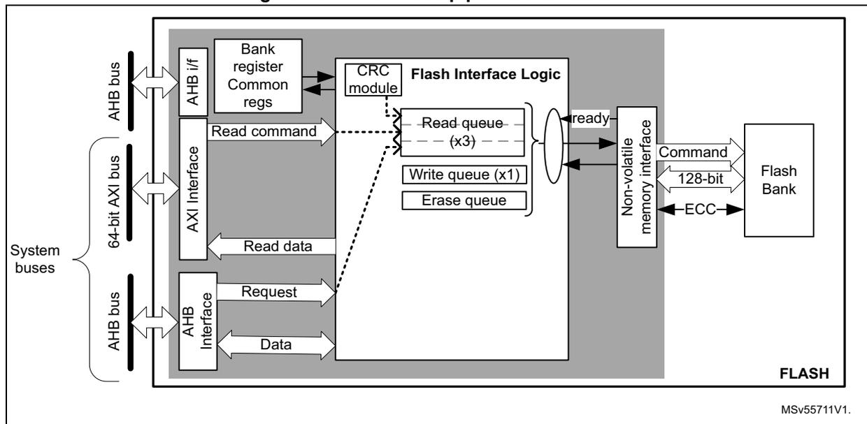
The embedded flash memory micro-architecture is shown in Figure 10.
Figure 10. Detailed FLASH architecture
The diagram illustrates the internal architecture of the embedded flash memory. On the left, three system interfaces are shown: an AHB bus, a 64-bit AXI bus, and another AHB bus. The AHB bus connects to an 'AHB if' block, which contains 'Bank register Common regs'. The 64-bit AXI bus connects to an 'AXI Interface' block. The second AHB bus connects to another 'AHB Interface' block. All three interface blocks feed into a central 'Flash Interface Logic' block. This logic block contains a 'CRC module', three 'Read queue (x3)' buffers, one 'Write queue (x1)', and an 'Erase queue'. A 'Non-volatile memory interface' block receives data from the queues and sends 'ready' signals back to the logic. This interface connects to a 'Flash Bank' via 'Command', '128-bit' data, and 'ECC' lines. The entire internal structure is labeled 'FLASH' at the bottom right. A reference code 'MSV55702V1.' is located at the bottom right of the diagram.
Behind the system interfaces, the embedded flash memory implements various command queues and buffers to perform flash read, write and erase operations with maximum efficiency.
By the addition of a read and write data buffer, the AXI slave port handles the following access types:
- • Multiple length: 64 bits, 32 bits, 16 bits and 8 bits
- • Single or burst accesses
- • Write wrap burst must not cross 16-byte aligned address boundaries to target exactly one flash word
The AHB system slave port supports only 16-bit or 32-bit word accesses. For 8-bit accesses, an AHB bus error is generated and write accesses are ignored.
The AHB configuration slave port supports 8-bit, 16-bit and 32-bit word accesses.
The embedded flash memory is built in such a way that only one read or write operation can be executed at a time.
5.3.4 Flash memory architecture and usage
Flash memory architecture
Figure 11 shows the non-volatile memory organization in the embedded flash memory.
Figure 11. Embedded flash memory organization
The diagram illustrates the internal organization of embedded flash memory. On the left, three interfaces are shown: the AXI system bus, the AHB system bus, and the AHB config port, all connected to a central 'Flash Interface Logic' block. The memory is divided into several functional areas:
- User flash: A block containing multiple sectors (Sector 0 (*), Sector 1, Sector 2, ..., Sector i). Sector 0 is marked with an asterisk (*), indicating it is bootable. This area is subject to a 'Hide protection area' mechanism.
- System flash: A block containing system sectors (Sys Sector 0 (*), Sys Sector 1, ..., Sys Sector j). Sys Sector 0 is also bootable. This area also benefits from a 'Hide protection area' mechanism.
- Read-only: A section containing the OTP (One-Time Programmable) area.
- Option bytes: A section containing Option byte keys L0 , Option byte keys L1 , Option byte keys L2 , and Option byte user words . These are accessible via the AHB config port.
The embedded flash non-volatile memory is composed of:
- • A 64 Kbyte user memory block, organized as one bank divided in 8 sectors of 8 Kbytes each. This bank features flash-word rows of 128 bits + 9 bits of ECC per word. A user-defined address range benefits from a hide protection mechanism.
- • A 128 Kbytes system memory block, organized as one bank divided in 16 sectors of 8 Kbytes each. The system flash memory features the same flash-word rows of 128 bits + 9 bits of ECC per word. A specific range, starting from the system boot sector, also benefit from a hide protection mechanism.
- • A set of non-volatile user option byte words, loaded at reset by the embedded flash memory and accessible by the application software only through the AHB configuration register interface.
- • Three sets of non-volatile option byte keys, loaded at any time by the application software through the AHB configuration register interface. All the option byte keys benefit from a hide protection mechanism.
- • A 1 Kbyte one-time-programmable (OTP) area that can be written only once by the application software.
- • A 512-byte read-only area written by STMicroelectronics during SoC manufacturing.
Note: The system flash memory cannot be programmed nor erased by any application. Since the OTP area has no specific protection, it must not be used to store confidential information.
The overall flash memory architecture and its corresponding access interface is summarized in Table 28 .
Table 28. Flash memory organization
| Flash memory area | Address range | Size (bytes) | Region name | Access interface | SSN (1) |
|---|---|---|---|---|---|
| User main memory | 0x0800 0000-0x0800 1FFF | 8 K | Sector 0 | AXI port | 0x0 |
| 0x0800 2000-0x0800 3FFF | 8 K | Sector 1 | 0x1 | ||
| ... | ... | ... | ... | ||
| 0x0800 E000-0x0800 FFFF | 8 K | Sector 7 | 0x7 | ||
| System memory | 0x1FF0 0000-0x1FF0 1FFF | 8 K | System sector 0 | AXI port | N/A (2) |
| ... | ... | ... | |||
| 0x1FF1 E000-0x1FF1 FFFF | 8 K | System sector 15 | |||
| Special region | 0x08FF F000-0x08FF F3FF | 1 K | OTP area | AHB system port | N/A (2) |
| 0x08FF F800-0x08FF FFFF | 512 | Read-only area | |||
| Option bytes | registers | - | User option bytes | Registers only | N/A |
1. SSN contains the target sector number for an erase operation. See
2. Cannot be erased by application software
Partition usage
In the life of the product embedded flash memory stores different kinds of data. Data availability also vary according to the hide protection level (HDPL) selected by the application at any given time. See Section 8: System configuration, boot and security (SBS) for more details.
For STM32H7R devices the typical flash usages are described on Figure 12 and below.
- 1. Device on a Nucleo board for s/w development, or in production warehouses.
- 2. Device is being provisioned with immutable root of trust firmware and root of trust keys on an untrusted OEM production line, using secure firmware install (SFI).
- 3. Device on the final personalization line of the customer, and as used in the final product.
Figure 12. Embedded flash memory usage (STM32H7R)
Legend
| 0 | 1 | Hide protection level | H/w integrity protection |
| 2 | 3 | (HDPL) | for development purpose (keys not shown) |
MSv55706V2
- 1. In this state OEM_PROVD option byte is not 0xB4
- 2. This boot code could be protected via the HDPL area refer to Section 5.5.5: Hide protected user flash area .
For STM32H7S devices the typical flash memory usage and options are described on Figure 13 and below:
- 1. Device on a Nucleo board for software development, or in production warehouses.
- 2. Device is being provisioned with updatable root of trust firmware and root of trust keys on an untrusted OEM production line, using Secure Keys Provisioning (SKP) service. Alternatively, the device is being provisioned with immutable root of trust firmware and root of trust keys on an untrusted OEM production line, using secure firmware install (SFI).
- 3. Device on the final personalization line of the customer, and as used in the final product
Figure 13. Embedded flash memory usage (STM32H7S)
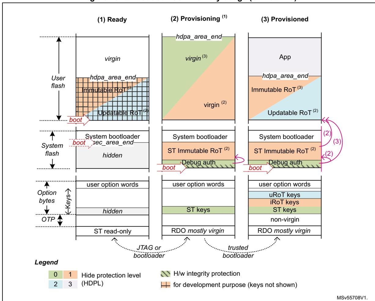
Legend
| 0 | 1 | Hide protection level | H/w integrity protection |
| 2 | 3 | (HDPL) | for development purpose (keys not shown) |
MSv55708V1.
- 1. In this state OEM_PROVD option byte is not 0xB4
- 2. ST iRoT is selected through IROT_SELECT option byte
- 3. OEM iRoT is selected through IROT_SELECT option byte. When OEM iRoT executes ST iRoT is hidden.
Figure 14 shows how the embedded flash memory is used when an OEM returns a provisioned production device to an open state (for field return to ST) or to a closed state to build a product. Two decommissioning scenarios are proposed:
- 1. Device opening for devices with OEM iRoT
- 2. Device opening for devices with ST iRoT (STM32H7S only).
Note: In any device, if application knows the decommissioning key it can open the device using STM32 tools.
Figure 14. Flash decommissioning options
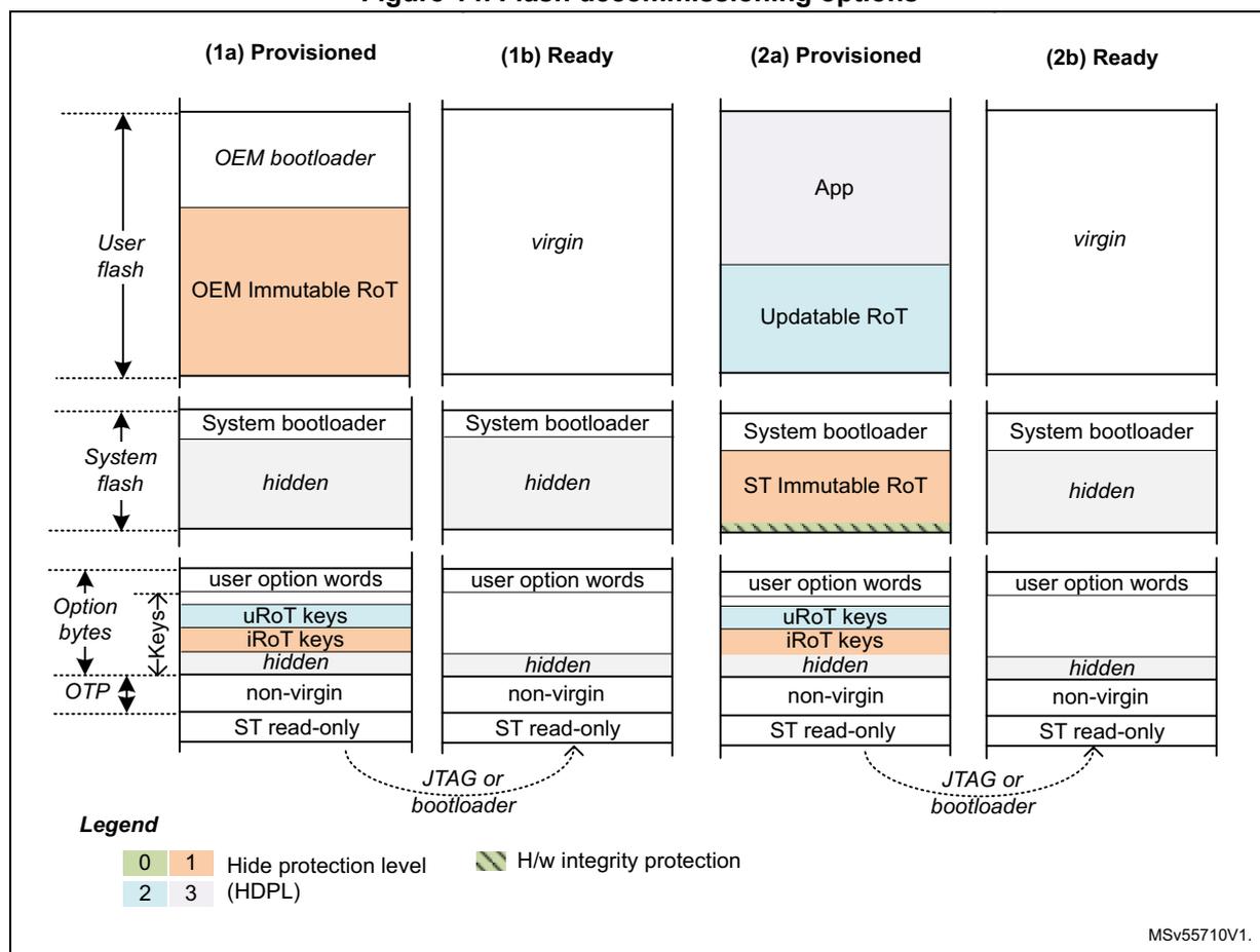
The diagram illustrates four flash memory layout options for decommissioning, categorized into 'Provisioned' and 'Ready' states for two different scenarios (1 and 2). Each column shows the state of User flash, System flash, Option bytes, and OTP.
- (1a) Provisioned: User flash contains 'OEM bootloader' and 'OEM Immutable RoT' (HDPL 1). System flash contains 'System bootloader' and a 'hidden' area (HDPL 0). Option bytes include 'user option words', 'uRoT keys' (HDPL 1), 'iRoT keys' (HDPL 1), and a 'hidden' area (HDPL 0). OTP contains 'non-virgin' and 'ST read-only' areas.
- (1b) Ready: User flash is 'virgin'. System flash contains 'System bootloader' and a 'hidden' area (HDPL 0). Option bytes include 'user option words' and a 'hidden' area (HDPL 0). OTP contains 'non-virgin' and 'ST read-only' areas.
- (2a) Provisioned: User flash contains 'App' and 'Updatable RoT' (HDPL 2). System flash contains 'System bootloader' and 'ST Immutable RoT' (HDPL 1) with H/w integrity protection. Option bytes include 'user option words', 'uRoT keys' (HDPL 2), 'iRoT keys' (HDPL 2), and a 'hidden' area (HDPL 0). OTP contains 'non-virgin' and 'ST read-only' areas.
- (2b) Ready: User flash is 'virgin'. System flash contains 'System bootloader' and a 'hidden' area (HDPL 0). Option bytes include 'user option words' and a 'hidden' area (HDPL 0). OTP contains 'non-virgin' and 'ST read-only' areas.
Legend:
| 0 | 1 | Hide protection level (HDPL) | H/w integrity protection |
| 2 | 3 |
MSv55710V1.
5.3.5 Flash hide protection schemes
Figure 11 gives an overview of the protection mechanism supported by the embedded flash memory:
- • A user flash area can be defined as user HDP area, with a hardware defined access policy based on STM32 hide protection level (HDPL).
- • A system flash starting from sector zero is defined as system HDP area, also with a hardware defined access policy based on STM32 hide protection level (HDPL).
- • Three sets of option byte keys are each reserved to a specific hide protection level. Some of those keys can be reserved to be used exclusively by the side channel attacks protected SAES engine, as application hardware keys (AHK).
For more information on both HDP areas, refer to Section 5.5.4: Hide protected system flash area and Section 5.5.5: Hide protected user flash area . More details on option byte keys can be found in Section 5.4.4: Option byte key management .
5.3.6 Overview of FLASH operations
Read operations
The embedded flash memory can perform read operations on the whole non-volatile memory using various granularities: 64 bits, 32 bits, 16 bits or one byte. User and system flash memories are read through the AXI interface, while the option bytes are read through the register interface. Read-only and OTP special region are read through the system AHB interface.
To increase efficiency, the embedded flash memory implements the buffering of consecutive read requests.
For more details on read operations, refer to Section 5.3.7: FLASH read operations .
Program/erase operations
The embedded flash memory supports the following program and erase operations:
- • Single flash word write (128-bit granularity for user flash memory, 16-bit granularity for OTP area), with the possibility for the application to force-write a user flash word with less than 128 bits in user flash memory
- • Single sector erase
- • Bank erase
- • Option byte words update, option byte key write (if allowed)
Note: Program and erase operations are subject to the various protection that could be set on the embedded flash memory (see next).
For more details, refer to Section 5.3.8: FLASH program operations and Section 5.3.9: FLASH erase operations .
Protection mechanisms
The embedded flash memory supports different protection mechanisms:
- • Configuration protection
- • Write protection
- • Temporal isolation enforcement of non-volatile secrets (code/data, keys), based on the hide protection level information stored in SBS_HDPLSR register.
- • Life cycle management, based on flash root of trust option bytes
- • OTP locking
For more details refer to Section 5.5: FLASH protection mechanisms .
Option byte loading
As part of the life cycle management, the embedded flash memory reliably loads the non-volatile option bytes stored in non-volatile memory after every power on reset, enforcing boot and security options to the whole device when the embedded flash memory becomes functional again. For more details refer to Section 5.4: FLASH option bytes .
5.3.7 FLASH read operations
Read operation overview
The embedded flash memory supports the execution of one read command while two are waiting in the read command queue. Multiple read access types are also supported as defined in Section 5.3.3: FLASH architecture and integration in the system .
The read commands is associated with a 128-bit read data buffer. These commands can be issued either by the AHB (OTP or read-only areas) or by the AXI interface (user flash or system flash memory).
Note: The embedded flash memory can perform single error correction and double error detection while read operations are being executed (see Section 5.3.10: Flash memory error protections ).
The AXI interface read channel operates as follows:
- • When the read command queue is full, any new AXI read request stalls the bus read channel interface and consequently the master that issued that request.
- • If several consecutive read accesses request data that belong to the same flash data word (128 bits), the data are read directly from the current data read buffer, without triggering additional flash read operations. This mechanism occurs each time a read access is granted. When a read access is rejected for security reasons (e.g. HDP protected word), the corresponding read error response is issued by the embedded flash memory and no read operation to flash memory is triggered.
The AHB system interface operates a follows:
- • Until the AHB read request has been served, the embedded flash memory stalls the AHB bus and consequently the master that issued that request.
The Read pipeline architecture is summarized in Figure 15 .
For more information on bus interfaces, refer to Section 5.3.3: FLASH architecture and integration in the system .
Figure 15. FLASH read pipeline architecture
The diagram illustrates the FLASH read pipeline architecture. On the left, 'System buses' are shown, including an 'AHB bus', a '64-bit AXI bus', and another 'AHB bus'. These buses connect to an 'AHB i/f' and an 'AXI Interface'. The 'AHB i/f' connects to 'Bank register Common regs' and 'CRC module'. The 'AXI Interface' connects to 'Flash Interface Logic', which contains a 'Read queue (x3)', 'Write queue (x1)', and 'Erase queue'. The 'CRC module' also connects to 'Flash Interface Logic'. The 'Flash Interface Logic' connects to a 'Non-volatile memory interface', which in turn connects to a 'Flash Bank'. The 'Flash Bank' sends 'Command', '128-bit' data, and 'ECC' signals back to the 'Non-volatile memory interface'. The 'Non-volatile memory interface' sends a 'ready' signal back to the 'Flash Interface Logic'. The 'Flash Interface Logic' sends 'Read command' and 'Read data' back to the 'AXI Interface', and 'Request' and 'Data' back to the 'AHB i/f'. The diagram is labeled 'FLASH' and 'MSv55711V1.' at the bottom right.
Single read sequence
The recommended simple read sequence is the following:
- 1. For AXI interface: Freely perform read accesses to any AXI-mapped area. For AHB interface: perform either 16-bit or 32-bit read accesses to the AHB-mapped area (byte accesses generate a bus error).
- 2. The embedded flash memory effectively executes the read operation from the read command queue buffer as soon as the non-volatile memory is ready and the previously requested operations have been served.
Note: When reading an OTP data that has not been previously written, a double ECC error is reported and only 1's are returned (see Section 5.3.11 for details).
Adjusting read timing constraints
The embedded flash memory clock must be enabled and running before reading data from non-volatile memory.
To correctly read data from flash memory, the number of wait states (LATENCY) must be correctly programmed in the flash access control register (FLASH_ACR) according to the embedded flash memory AXI interface clock frequency (sys_ck) and the internal voltage range of the device ( \( V_{core} \) ).
Table 29 shows the correspondence between the number of wait states (LATENCY), the programming delay parameter (WRHIGHFREQ), the embedded flash memory clock frequency and its supply voltage ranges.
Table 29. FLASH recommended read wait states and programming delays
| Wait states per flash word read (LATENCY) | Read latency (cycles per flash word) | Programming delay (WRHIGH FREQ) | AXI Interface clock frequency v.s. \( V_{CORE} \) range | |
|---|---|---|---|---|
| VOS low range 1.15 V - 1.26 V | VOS high range 1.30 V - 1.40 V | |||
| 0x0 | 1 | 00 | [0MHz ; 36MHz] | [0MHz ; 40MHz] |
| 0x1 | 2 | [36MHz ; 72MHz] | [40MHz ; 80MHz] | |
| 0x2 | 3 | 01 | [72MHz ; 108MHz] | [80MHz ; 120MHz] |
| 0x3 | 4 | [108MHz ; 144MHz] | [120MHz ; 160MHz] | |
| 0x4 | 5 | 10 | [144MHz ; 180MHz] | [160MHz ; 200MHz] |
| 0x5 | 6 | [180MHz ; 216MHz] | [200MHz ; 240MHz] | |
| 0x6 | 7 | 11 | N/A | [240MHz ; 280MHz] |
| 0x7 | 8 | 11 | N/A | [280 MHz; 320 MHz] |
Adjusting the system frequency
After power-on, the embedded flash memory is clocked by the 64 MHz high-speed internal oscillator (HSI), with a voltage range set at VOS low.
When changing the AXI bus frequency, the application software must follow the below sequence in order to tune the number of wait states required to access the non-volatile memory.
To increase the embedded flash memory clock source frequency:
- 1. If necessary, program the LATENCY and WRHIGHFREQ bits to the right value in the FLASH_ACR register, as described in Table 29 .
- 2. Check that the new number of wait states is taken into account by reading back the FLASH_ACR register.
- 3. Modify the embedded flash memory clock source and/or the AXI bus clock prescaler in the RCC_CFGR register of the reset and clock controller (RCC).
- 4. Check that the new embedded flash memory clock source and/or the new AXI bus clock prescaler value are taken in account by reading back the embedded flash memory clock source status and/or the AXI bus prescaler value in the RCC_CFGR register of the reset and clock controller (RCC).
To decrease the embedded flash memory clock source frequency:
- 1. Modify the embedded flash memory clock source and/or the AXI bus clock prescaler in the RCC_CFGR register of reset and clock controller (RCC).
- 2. Check that the embedded flash memory new clock source and/or the new AXI bus clock prescaler value are taken into account by reading back the embedded flash memory clock source status and/or the AXI interface prescaler value in the RCC_CFGR register of reset and clock controller (RCC).
- 3. If necessary, program the LATENCY and WRHIGHFREQ bits to the right value in FLASH_ACR register, as described in Table 29 .
- 4. Check that the new number of wait states has been taken into account by reading back the FLASH_ACR register.
Read errors
The embedded flash memory embeds an error correction mechanism, as described in Section 5.3.10 .
Single error correction and double error detection are performed for each read operation. In both cases the embedded flash memory reports read errors as described in Section 5.7.6: Error correction code error (SNECCERRF/DBECCERRF) .
Read interrupts
See Section 5.8: FLASH interrupts for details.
5.3.8 FLASH program operations
Program operation overview
The virgin state of each non-volatile memory bitcell is 1. The embedded flash memory supports programming operations that can change any memory bitcell to 0. However these operations do not support the return of a bit to its virgin state. In this case an erase operation of the entire sector is required.
Program operation consists in issuing write commands. For write accesses issued by the AXI interface, since a 9-bit ECC code is associated to each 128-bit data flash word, the embedded flash memory must always perform write operations to non-volatile memory with a 128-bit word granularity.
Note: The application can decide to write as few as 8 bits to a 128-bit flash word. In this case, a force-write mechanism to the 128 bits + ECC is used (see FW bit of FLASH_CR register). System flash memory cannot be written by the application software.
It is not recommended to overwrite a flash word that is not virgin. The result may lead to an inconsistent ECC code that is systematically reported by the embedded flash memory, as described in Section 5.7.6: Error correction code error (SNECCERRF/DBECCERRF) .
Write access requests issued by the AHB system interface are serialized with AXI commands and can only be used to program the memory OTP area. In this area, since a 6-bit ECC code is associated to each 16-bit data flash word, the embedded flash memory supports 16-bit or 32-bit write operations (8-bit write operations are not supported).
Note: The OTP area is typically write-protected on the final product, as described in Section 5.3.11: FLASH one-time programmable area . Erase operations to the OTP area are not supported.
The AXI interface write channel operates as follows:
- • A 128-bit write data buffer is associated with the AXI interface. It supports multiple write access types (64 bits, 32 bits, 16 bits and 8 bits).
- • When the write queue is full, any new AXI write request stalls the bus write channel interface and consequently the master that issued that request.
The AHB system interface operates as follows:
- • Write commands issued by the AHB system interface are associated with a 137-bit flash word buffer. Byte accesses are not supported.
- • When the write queue is full, any new AHB request stalls the bus interface and consequently the master that issued that request.
The write pipeline architecture is described in Figure 16 .
For more information on bus interfaces, refer to Section 5.3.3: FLASH architecture and integration in the system .
Figure 16. FLASH write pipeline architecture
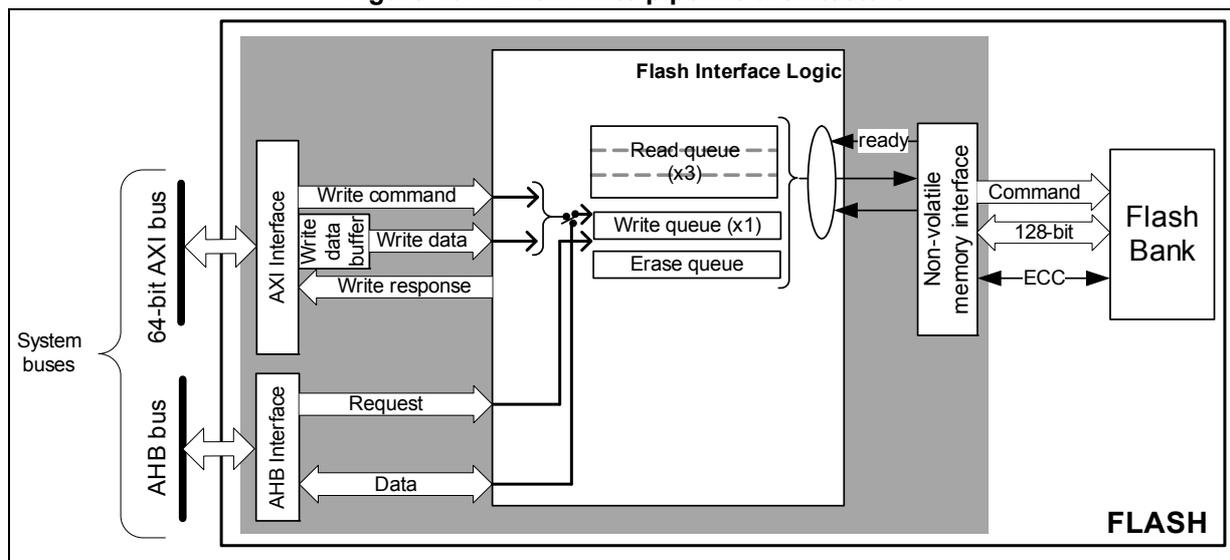
The diagram illustrates the FLASH write pipeline architecture. On the left, 'System buses' are shown, consisting of a '64-bit AXI bus' and an 'AHB bus'. The AXI bus connects to an 'AXI Interface' block, which sends 'Write command', 'Write data' (via a 'Write data buffer'), and receives a 'Write response'. The AHB bus connects to an 'AHB Interface' block, which sends a 'Request' and receives 'Data'. Both interfaces feed into 'Flash Interface Logic'. Inside this logic, there are three 'Read queue (x3)' blocks, one 'Write queue (x1)' block, and an 'Erase queue' block. A 'ready' signal is passed from the queues to a 'Non-volatile memory interface' block. This interface sends a 'Command', '128-bit' data, and an 'ECC' code to the 'Flash Bank' on the right. The entire internal structure is labeled 'FLASH' at the bottom right.
Managing write protections
Before programming a user sector, the application software must check the protection of the targeted flash memory area.
The embedded flash memory checks the protection properties of the write transaction target at the output of the write queue buffer, just before the effective write operation to the non-volatile memory:
- • If a write protection violation is detected, the write operation is canceled and write protection error (WRPERRF) is raised in FLASH_ISR register.
- • If the write operation is valid, the 9-bit ECC code is concatenated to the 128 bits of data and the write to non-volatile memory is effectively executed.
Note: No write protection check is performed when the embedded flash memory accepts AXI write requests.
A similar mechanism exists for OTP areas with the following differences:
- • If the write operation is valid, the 6-bit ECC code is concatenated to the 16 bits of data and the write to non-volatile memory is effectively executed.
The write protection flag does not need to be cleared before performing a new programming operation.
Monitoring ongoing write operations
The application software can use three status flags located in FLASH_SR in order to monitor ongoing write operations.
- • BUSY : this bit indicates in real-time that an effective write, erase or option byte change operation is ongoing to the non-volatile memory. It is possible to know what type of
operation is being executed polling the bits IS_PROGRAM, IS_ERASE and IS_OPTCHANGE in the same register.
- • QW : this bit indicates that a write, erase or option byte change operation is pending in the write queue or command queue buffer. It remains high until the write operation is complete. It supersedes the BUSY status bit.
- • WBNE : this bit indicates that the embedded flash memory is waiting for new data to complete the 128-bit write buffer. In this state the write buffer is not empty. It is reset as soon as the application software fills the write buffer, force-writes the operation using FW bit in FLASH_CR, or disables all write operations.
Enabling write operations
Before programming the user flash memory, the application software must make sure that PG bit is set in FLASH_CR. If it is not set an unlock sequence must be used once (see Section 5.5.1: FLASH configuration protection ) and the PG bit must be set.
Before programming an option byte word or an option byte key, the application software must make sure that PG_OPT bit is set in FLASH_OPTCR. If it is not set an unlock sequence must be used once (see Section 5.5.1: FLASH configuration protection ). For more information on option byte word (resp. option byte key) modification, refer to Section 5.4.3 (or Section 5.4.4 respectively).
Note: The application software must not unlock a register that is already unlocked, otherwise this register remains locked until next system reset.
If needed, the application software can update the programming delay as described at the end of this section.
Single write sequence
The recommended single write sequence is the following:
- 1. Unlock the FLASH_CR register, as described in Section 5.5.1: FLASH configuration protection (only if register is not already unlocked).
- 2. Enable write operations by setting the PG bit in the FLASH_CR register.
- 3. Check the protection of the targeted memory area.
- 4. Write one flash-word corresponding to 16-byte data starting at 16-byte aligned address.
- 5. Check that QW has been raised and wait until it is cleared to 0.
If step 4 is executed incrementally (for example byte per byte), the write buffer can become partially filled. In this case the application software can decide to force-write what is stored in the write buffer by using FW bit in FLASH_CR register. In this particular case, the unwritten bits are automatically set to 1. If no bit in the write buffer is cleared to 0, the FW bit has no effect.
Note: Using a force-write operation prevents the application from updating later the missing bits with a value different from 1, which is likely to lead to a permanent ECC error.
Any write access requested while the PG bit is cleared to 0 is rejected. In this case, no error is generated on the bus, but the PGSERRF flag is raised.
Clearing the programming sequence error (PGSERRF) and inconsistency error (INCERRF) is mandatory before attempting a write operation (see Section 5.7: FLASH error management for details).
Adjusting programming timing constraints
Program operation timing constraints depend of the embedded flash memory clock frequency, which directly impacts the performance. If timing constraints are too tight, the non-volatile memory does not operate correctly, if they are too lax, the programming speed is not optimal.
The user must therefore trim the optimal programming delay through the WRHIGHFREQ parameter in the FLASH_ACR register. Refer to Table 29 in Section 5.3.7: FLASH read operations for the recommended programming delay depending on the embedded flash memory clock frequency.
The application software must check that no program/erase operation is ongoing before modifying WRHIGHFREQ parameter.
Caution: Modifying WRHIGHFREQ while programming/erasing the flash memory might corrupt the flash memory content.
Programming errors
When a program operation fails, an error can be reported as described in Section 5.7: FLASH error management .
Programming interrupts
See Section 5.8: FLASH interrupts for details.
5.3.9 FLASH erase operations
Erase operation overview
The embedded flash memory can perform erase operations (if allowed) on 8-Kbyte user sectors or on the whole user flash memory.
Note: System flash memory and read-only/OTP area cannot be erased by the application software.
The erase operation forces all non-volatile bit cells to high state, which corresponds to the virgin state. It clears existing data and corresponding ECC, allowing a new write operation to be performed. If the application software reads back a word that has been erased or not programmed, all the bits are read at 1. No ECC error is generated if the word is located in user flash memory, while a double ECC error is raised if the word is located in read-only or OTP area.
Erase operations are similar to read or program operations except that the commands are queued in a special buffer (a one-command deep erase queue).
Erase commands are issued through the AHB configuration interface. If the embedded flash memory receives simultaneously a write and an erase request, both operations are accepted but the write operation is executed first.
Erase and security
A user sector can be erased only if it does not contain hide protected or write-protected data (see Section 5.5: FLASH protection mechanisms for details). In other words, if the application software attempts to erase a user sector with at least one flash word that is protected, the sector erase operation is aborted and the WRPERRF flag is raised in the FLASH_ISR register, as described in Section 5.7.2 .
The only method to erase HDP protected sectors is to perform a regression, triggering a NVSTATE change from CLOSE to OPEN. See Section 5.5.3 for details.
Enabling erase operations
Before erasing a sector, the application software must make sure that FLASH_CR is unlocked. If it is not the case, an unlock sequence must be used (see Section 5.5.1: FLASH configuration protection ).
Note: The application software must not unlock a register that is already unlocked, otherwise this register remains locked until next system reset.
Similar constraints apply to bank erase requests.
Flash sector erase sequence
To erase a 8-Kbyte user sector, proceed as follows:
- 1. Check and clear (optional) all the error flags due to previous programming/erase operation. Refer to Section 5.7: FLASH error management for details.
- 2. Unlock the FLASH_CR register, as described in Section 5.5.1: FLASH configuration protection (only if register is not already unlocked).
- 3. Set the SER bit and SSN bitfield in the corresponding FLASH_CR register. SER indicates a sector erase operation, while SSN contains the target sector number.
- 4. Set the START bit in the FLASH_CR register.
- 5. Wait for the QW bit to be cleared in the FLASH_SR register.
Note: If a bank erase is requested simultaneously to the sector erase (BER and SER bits set), the bank erase operation supersedes the sector erase operation.
Flash bank erase sequence
To erase all bank sectors except for those containing hide protected data, proceed as follows:
- 1. Check and clear (optional) all the error flags due to previous programming/erase operation. Refer to Section 5.7: FLASH error management for details.
- 2. Unlock the FLASH_CR register, as described in Section 5.5.1: FLASH configuration protection (only if register is not already unlocked).
- 3. Set the BER bit in the FLASH_CR register .
- 4. Set the START bit in the FLASH_CR register to start the bank erase operation. Then wait until the QW bit is cleared in FLASH_SR register.
Note: BER and START bits can be set together, so above steps 3 and 4 can be merged.
If a sector erase is requested simultaneously to the bank erase (SER bit set), the bank erase operation supersedes the sector erase operation.
5.3.10 Flash memory error protections
Error correction codes (ECC)
The embedded flash memory supports an error correction code (ECC) mechanism. It is based on the SECDED algorithm in order to correct single errors and detects double errors.
Per 128-bit system and user flash word the embedded flash memory uses 9 ECC bits. During each read operation from a 128-bit flash word, FLASH retrieves the 9-bit ECC information, computes the ECC of the flash word, and compares the result with the reference value. If they do not match, the corresponding ECC error is raised as described in Section 5.7.6: Error correction code error (SNECCERRF/DBECCERRF) . During each program operation, a 9-bit ECC code is associated to each 128-bit data flash word, and the resulting 137-bit flash word information is written in non-volatile memory.
For read-only and OTP areas, the embedded flash memory uses a stronger 6 ECC bits per 16-bit word. For option byte words and keys a double ECC scheme is used. For more information on read-only and OTP refer to Section 5.3.11 and Section 5.3.12 . For more information on option byte words and keys refer to Section 5.4 .
Note: A double ECC error is generated for an OTP virgin word (i.e. a word with 22 bits at 1). When this OTP word is no more virgin, the ECC error disappears.
Cyclic redundancy codes (CRC)
The embedded flash memory implements a cyclic redundancy check (CRC) hardware module. This module checks the integrity of a given user flash memory area content.
The area processed by the CRC module can be defined either by sectors or by start/end addresses.
When enabled, the CRC hardware module performs multiple reads by chunks of 4, 16, 64 or 256 consecutive flash-word (i.e. chunks of 64, 256, 1024 or 4096 bytes). These consecutive read operations are pushed by the CRC module into the required read command queue together with other AXI read requests, thus avoiding to deny AXI read commands.
CRC computation uses CRC-32 (Ethernet) polynomial 0x4C11DB7:
The CRC operation is concurrent with the reading or writing of option byte user words, keys or OTP, because the same hardware is used for all those operations. To avoid corruption to the CRC computation the flash stalls above incoming requests when a CRC operation is ongoing.
The sequence recommended to configure a CRC operation is the following:
- 1. Unlock FLASH_CR register, if not already unlocked.
- 2. Enable the CRC feature by setting the CRC_EN bit in FLASH_CR.
- 3. Program the desired data size in the CRC_BURST field of FLASH_CRCCR.
- 4. Define the user flash memory area on which the CRC has to be computed. Three solutions are possible:
- – Select all user flash sectors by setting the ALL_SECT bit in FLASH_CRCCR
- – Define the area start and end addresses by programming FLASH_CRCSTART and FLASH_CRCEND, respectively,
- – Select the targeted sectors by setting the CRC_BY_SECT bit in FLASH_CRCCR. Also program consecutively the target sector numbers using the CRC_SECT field
of the FLASH_CRCCR register. Set ADD_SECT bit after each CRC_SECT programming.
- 5. When step 4 is completed start the CRC operation by setting the START_CRC bit in FLASH_CRCCR.
- 6. Wait until the CRC_BUSY flag is reset in FLASH_SR.
- 7. Retrieve the CRC result in FLASH_CRCDATAR.
Note: The application should avoid running a CRC on HDP user flash memory area when the hide protection level prevents access to it. Indeed, doing so may alter the expected CRC value. A special error flag defined in Section 5.7.8: CRC read error (CRCRDERRF) can be used to detect such a case.
CRC computation does not raise standard read error flags such as RDSERRF and DBECCERRF. Only CRCRDERRF is raised.
5.3.11 FLASH one-time programmable area
The embedded flash memory offers a 1024-byte memory area dedicated to application non-confidential one-time programmable data (OTP). It is composed of 512 words of 16 bits that cannot be erased, and can be written only once.
Note: The OTP area is virgin when the device is delivered by STMicroelectronics.
OTP data can be accessed through the AHB system port. They are organized as 16 blocks of 32 OTP words, as shown in Table 30 . An entire OTP block can be protected (locked) from write accesses by setting the corresponding OTPL bit in the FLASH_OTPLSRP register, as shown. There is no special read protection mechanism on the OTP area.
Note: The OTP block locking operation is irreversible and independent from the life cycle management described in Section 5.5.3 .
A block can be write-protected whether or not it has been programmed (even partially).
Table 30. Flash memory OTP organization
| OTP block | AHB address | AHB word | Lock bit | |
|---|---|---|---|---|
| [31:16] | [15:0] | |||
| Block 0 | 0x08FF F000 | OTP001 | OTP000 | OTPL[0] |
| 0x08FF F004 | OTP003 | OTP002 | ||
| ... | ||||
| 0x08FF F03C | OTP031 | OTP030 | ||
| Block 1 | 0x08FF F040 | OTP033 | OTP032 | OTPL[1] |
| 0x08FF F044 | OTP035 | OTP034 | ||
| ... | ||||
| 0x08FF F07C | OTP063 | OTP062 | ||
| Block 2 | 0x08FF F080 | OTP065 | OTP064 | OTPL[2] |
| 0x08FF F084 | OTP067 | OTP066 | ||
| ... | ||||
| 0x08FF F0BC | OTP127 | OTP126 | ||
Table 30. Flash memory OTP organization (continued)
| OTP block | AHB address | AHB word | Lock bit | |
|---|---|---|---|---|
| [31:16] | [15:0] | |||
| ... | ||||
| Block 15 | 0x08FF F3C0 | OTP481 | OTP480 | OTPL[15] |
| 0x08FF F3C4 | OTP483 | OTP482 | ||
| ... | ||||
| 0x08FF F3FC | OTP511 | OTP510 | ||
OTP error protection
OTP data are organized as 16 blocks of 32 OTP words, as shown on Table 30 . Each 16-bit half-word is protected by 6 bits of ECC. Hence application must avoid overwriting a 16-bit half-word that has already been programmed, as it is leading to systematic ECC error. Similarly, do not write twice an 16-bit OTP word, as it could lead to systematic ECC error.
When reading OTP data with a single error corrected or a double error detected, the embedded flash memory reports the corresponding error, as described in Section 5.7.6: Error correction code error (SNECCERRF/DBECCERRF) .
When reading OTP data that has not been written by the application software (that is, virgin OTP), the ECC correction reports a double error detection (DBECCERRF), and all 1's are returned. It is therefore recommended that the application always writes the OTP data before trying to read it.
OTP write sequence
Follow the sequence below to write an OTP word:
- 1. Check the protection status of the target OTP word (see Table 30 ). The corresponding OTPLi bit must be cleared in FLASH_OTPLSR register.
- 2. Unlock FLASH_CR if the register is not already unlocked, and then set PG_OTP bit in the FLASH_CR register.
- 3. Write two OTP words (32 bits) corresponding to the 4-byte aligned address shown in Table 30 . Alternatively, the application software can program separately the 16-bit MSB or 16-bit LSB. In this case the first 16-bit write operation starts immediately without waiting for the second one.
- 4. Check that the QW bit in FLASH_SR has been set and wait until it is cleared.
- 5. Read back the target OTP word to confirm the value
- 6. Optionally, lock the OTP block using OTPLi bit in FLASH_OTPLSRP in order to prevent further data changes. PG_OTP bit in the FLASH_CR register can also be cleared if needed.
Note:
To avoid data corruption, it is important to complete the OTP write process (for example by reading back the OTP value), before starting a new option byte change.
No error sequence and no inconsistency error are generated during OTP write operations.
Writing OTP data at byte level is not supported and generates a bus error.
5.3.12 FLASH read-only area
The embedded flash memory offers a 512-byte memory area dedicated to non-confidential and read-only information usable by application software.
Read-only area can be accessed through the AHB system port. It is organized as shown in Table 31 . This information is provisioned by STMicroelectronics during the device manufacturing.
Table 31. Read-only public data organization
| AHB address (read-only) | Read-only data name and usage |
|---|---|
| 0x08FF F800 | U_ID[31:0] |
| 0x08FF F804 | U_ID[63:32] |
| 0x08FF F808 | U_ID[95:64] |
| 0x08FF F80C | Package code[15:0] |
| 0x08FF F810 to 0x08FF F9FF | Reserved information |
Read-only area error protection
Read-only area is protected by a robust ECC scheme. When reading a 32-bit word in this area with a single error corrected or a double error detected, the embedded flash memory reports the corresponding error, as described in Section 5.7.6: Error correction code error (SNECCERRF/DBECCERRF) .
5.3.13 FLASH reset and clocks
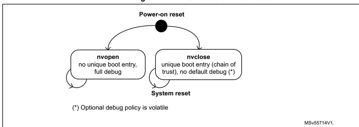
Reset management
Following a power-on reset embedded flash selects two security states, as shown on Figure 17 . For more details on those states, refer to Section 5.5.3 .
Figure 17. FLASH stateful initialization
graph TD
    POR((Power-on reset)) --> nvopen[nvopen
no unique boot entry,
full debug]
    POR --> nvclose[nvclose
unique boot entry (chain of
trust), no default debug (*)]
    nvopen --> SR((System reset))
    nvclose --> SR
(*) Optional debug policy is volatile
MSV55714V1.
Embedded flash memory stateful initialization is based on the overloading of option bytes default values by non-volatile values automatically loaded when the reset signal rises.
During this loading sequence, other parts of the device remains under reset and the embedded flash memory is not accessible from its interfaces.
The embedded flash memory can be reset at any time by the application through the RCC peripheral, with the following effects:
- • All registers, except for option byte registers, are cleared, including read and write latencies. Option byte register list is found in Section 5.4.5 .
- • Most control registers are automatically protected against write operations, as described in Section 5.5.1: FLASH configuration protection .
It is important to note that the contents of the flash memory (except option bytes) are not guaranteed if a power-on-reset occurs during a flash memory write or erase operation. For option bytes a valid content is always guaranteed, as embedded flash uses the old option byte values when an option byte modification is interrupted by a reset. In this case a new option byte change request must be issued to modify those option bytes.
Clock management
The embedded flash memory uses the AXI interface clock. Depending on the device clock and internal supply voltage, specific read and write latency settings usually need to be set in the flash access control register (FLASH_ACR), as explained in Section 5.3.7: FLASH read operations and Section 5.3.8: FLASH program operations .
5.4 FLASH option bytes
5.4.1 About option bytes
The embedded flash memory includes a set of non-volatile option bytes that are either freely modified through configuration registers (option byte words), or are managed as non-volatile keys with a special temporal isolation protection mechanism.
This section explains:
- • how option byte words and keys are loaded
- • how application software can change option byte words, under which conditions
- • how application software can program option byte keys
- • what is the detailed list of option byte words, together with their default factory values (that is, before the first option byte change).
5.4.2 Option byte loading
When the device is first powered, the embedded flash memory automatically loads all the option byte words, and few selected option byte keys. During the option byte loading sequence, the device remains under reset and the embedded flash memory cannot be accessed.
When an ECC issue is detected during this option byte loading sequence OBLERRF flag is raised, as described in Section 5.7.12 .
5.4.3 Option byte words modification
Changing option byte words
A option byte word change operation can modify the configuration and the protection settings saved in the non-volatile option byte area, if allowed.
The embedded flash memory features two sets of option byte words registers:
- • The first register set contains the current values of the option bytes. Their names have the SR extension. All “SR” registers are read-only. Unless documented otherwise, their values are automatically loaded from the non-volatile memory after power-on reset, or after a successful option byte change operation.
- • The second register set allows the modification of the option bytes. Their names ends with the SRP extension. All “SRP” registers can be accessed in read/write mode.
Note: When the OPTLOCK bit in FLASH_OPTCR register is set, writes to SRP registers are ignored.
When option byte word register “SRP” is written the embedded flash memory checks if at least one option byte needs to be programmed by comparing the current values in corresponding “SR” register. If a change is detected, if associated change conditions are met (see Changing security option bytes ) and if PG_OPT bit is set in FLASH_OPTCR, the embedded flash memory launches the option byte modification in its non-volatile memory and update the “SR” register.
If one of the condition described in Changing security option bytes is not respected, the embedded flash memory sets the OPTERRF flag in the FLASH_OPTISR register and aborts the option byte change operation.
Unlocking the option byte modification
After reset, the OPTLOCK bit is set and the FLASH_OPTCR is locked. As a result, the application software must unlock the option configuration register before attempting to change the option byte words, setting PG_OPT bit. The FLASH_OPTCR unlock sequence is described in Section 5.5.1
Option byte modification sequence
To modify an option byte word, follow the sequence below:
- 1. Unlock FLASH_OPTCR register as described in Section 5.5.1: FLASH configuration protection (only if the register is not already unlocked).
- 2. Enable the write operations by setting the PG_OPT bit in FLASH_OPTCR.
- 3. Write the desired new option byte values in the corresponding option byte word register (FLASH_xSRP).
- 4. Wait until the QW bit is cleared in FLASH_SR register. Once cleared corresponding FLASH_xSR register has been updated, if security allows it (see next section).
Note: If a reset or a power-down occurs while the option byte words modification is ongoing, the original option byte value are kept. A new option byte modification sequence is required to program the new value.
Changing security option bytes
On top of OPTLOCK bit, there is a second level of protection for security-sensitive option byte words. Note that the option byte words defined in Section 5.4.5 do not have any special protection.
Option byte words with specific protections are described hereafter.
- • Sector write protection (WRPS)
Those user options managing group of sector write protection can be changed using FLASH_WRPSRP register, if application is RSS or the immutable root of trust.
- • Non-volatile state (NVSTATE)
A detailed description of NVSTATE option bits is given in Section 5.5.3 . The following rules must be respected to modify NVSTATE using FLASH_NVSRP register.
- – Writes to FLASH_NVSRP register are ignored if HDPL is different from 0 or 1 in SBS_HDPLSR register.
- – NVSTATE option change is triggered only after the RAM erase signal has confirmed that Backup RAM and PKA RAM have been successfully erased.
- – When NVSTATE=OPEN, option byte change to CLOSE is allowed. Writing any other value than 0x51 triggers an OPTERRF flag, without option change.
- – When NVSTATE=CLOSE, option byte change to OPEN is allowed, triggering a global erase explained in Section 5.5.3 . Writing any other value than 0xB4 triggers an OPTERRF flag, without option change.
- • OEM provisioned (OEM_PROVD)
As defined in Table 36: Boot level and HDP area protections (non STiRoT case) , OEM_PROVD defines the protection of the HDP area. OEM_PROVD can only be changed by RSS in FLASH_ROTSRP.
- • iRoT selection (IROT_SELECT)
As defined in Table 37: Boot level and HDP area protections (STiRoT case) , IROT_SELECT defines where the immutable root of trust code is stored, for STM32H7S devices only. IROT_SELECT can only be changed when the device is opened by RSS in FLASH_ROTSRP.
- • Debug authentication method (DBG_AUTH)
DBG_AUTH defines the method used to open up the device debug. It has no hardware effect in embedded flash memory.
DBG_AUTH can only be changed by RSS in FLASH_ROTSRP.
- • Secure storage counter (EPOCH)
This 24-bit non-volatile value is directly sent by embedded flash to the SAES peripheral. As soon as this value changes all current keys encrypted with a derived hardware unique key (DHUK) are lost. For more details on the DHUK, refer to SAES chapter. EPOCH can only be changed by RSS.
- • Hide protection area size (HDP_AREA_START and HDP_AREA_END)
These user options configure the size of the user flash area that can be accessed while HDPL equals to the value defined in Section 5.5.5 . Writes to FLASH_HDPSRP register are ignored if HDPL is different from 0 or 1 in the SBS_HDPLSR register.
Note: For all user option bytes in this section: default values are loaded when a double ECC error occurs. OBLERRF error flag is also raised.
Hide protection area end address in system flash is fixed by STMicroelectronics.
5.4.4 Option byte key management
Option byte key programming
Following sequence is required to program an option byte key in embedded flash memory:
- 1. Unlock FLASH_OPTCR register as described in Section 5.5.1: FLASH configuration protection (only if the register is not already unlocked).
- 2. Enable the write operation by setting the PG_OPT bit in FLASH_OPTCR, and make sure the KTEF and KVEF bits are cleared in FLASH_OPTISR.
- 3. Write the key value in the FLASH_OBKDRx registers. Key[31:0] goes in OBKDR0[31:0], Key[63:32] to OBKDR1[31:0], Key[95:64] to OBKDR2[31:0], Key[127:96] to OBKDR3[31:0], Key[159:128] to OBKDR4[31:0], Key[191:160] to OBKDR5[31:0], Key[223:192] to OBKDR6[31:0] and Key[255:224] to OBKDR7[31:0].
- 4. Fill the following information to FLASH_OBKCR:
- – OBKINDEX[4:0]: index of the key for this hide protection level
- – OBKSIZE[1:0]: size of the key (see bitfield description)
- – NEXTKL[1:0]: when HDPL=1 in SBS_HDPLSR register RoT application can set those bit to 01 to provision a key for the next HDPL level (2).
- – Set both KEYSTART and KEYPROG bits to start the programming sequence.
- 5. Read back the key to verify its value (recommended). See Option byte key loading .
Note: When HDPL value in SBS peripheral changes FLASH_OBKDR register is cleared to 0x0.
For a given hide protection level, if authorized the application writes to an OBKINDEX that has already being successfully used before the old key is overwritten with the new value.
Like for any option change, if an error occurs OPTERRF is set in FLASH_OPTISR. It must be cleared, like KTEF and KVEF, before initiating another option byte key programming (otherwise the setting of KEYSTART bit is ignored).
All key error flags (KVEF, KTEF) must be cleared before application reads or write an option byte key.
Note: Option byte key integrity could fail when a reset is issued while programming it. When this happens the previously written key is kept, and no key is returned if it was the first programming. The OBLERRF error flag is also raised.
Option byte key loading
If OBKINDEX[4:0] is or greater than or equal to 0x8, the following sequence is required to read an option byte key stored in embedded flash memory:
- 1. Fill the following information to FLASH_OBKCR:
- – OBKINDEX[4:0]: index of the key for this hide protection level. Size of the key is automatically recovered from the flash memory.
- – NEXTKL[1:0]: when HDPL=1 in SBS_HDPLSR register RoT application can set those bit to 01 to read a key provisioned for the next HDPL level (2).
- – Set KEYSTART bit with KEYPROG bit cleared to start the read sequence.
- 2. Wait until QW bit is cleared in FLASH_SR register.
- 3. Read the value of the key using FLASH_OBKDRx registers
If OBKINDEX[4:0] is less than 0x8, the following sequence is required to load to the SAES peripheral an option byte key stored in embedded flash.
- 1. In the SAES peripheral, set the correct KEYSIZE and write KEYSEL[2:0] =011 or 101 in the SAES_CR register.
- 2. Perform the same sequence as a normal option byte key read, with the exception of reading back the FLASH_OBKDRx registers. In this case, key data are automatically transferred from embedded flash memory to the SAES key registers, while the BUSY bit is set in the SAES_SR register.
- 3. Once the transfer is completed the BUSY bit is cleared and the KEYVALID bit is set in the SAES_SR register. If KEYVALID is not set when the BUSY bit is cleared, or if a key error flag (KEIF) is set in SAES, this means that an unexpected event occurred during the transfer. In this unlikely event the IPRST bit must be set then cleared in the SAES_CR register, then sequence can be restarted from Step 1 above.
During option byte key loading two errors can happen:
- • Key valid error (see Section 5.7.10 )
- • Key transfer error (see Section 5.7.11 )
All key error flags (KVEF, KTEF) must be cleared before application reads or writes an option byte key.
Note: When the HDPL value in the SBS peripheral changes, the FLASH_OBKDR register is cleared to 0x0.
5.4.5 Option byte user words overview
Table 32 lists all the user option bytes managed through the embedded flash memory registers, as well as their default values before the first option byte change (default factory value). They are configured by the end-user depending on the application requirements. Some option bytes might have been initialized by STMicroelectronics during manufacturing stage.
Table 32. Option byte user words organization
| Register | Bitfield | |||||||||||||||
|---|---|---|---|---|---|---|---|---|---|---|---|---|---|---|---|---|
| 31 | 30 | 29 | 28 | 27 | 26 | 25 | 24 | 23 | 22 | 21 | 20 | 19 | 18 | 17 | 16 | |
| FLASH_OBW1SR[31:16] | Res. | Res. | VDDIO_HSLV | Res. | Res. | Res. | Res. | Res. | Res. | Res. | Res. | Res. | Res. | FW_IWDG_STBY | FW_IWDG_STOP | Res. |
| Default factory value | 0 | 0 | 0 | 0 | 0 | 0 | 0 | 0 | 0 | 0 | 0 | 0 | 0 | 1 | 1 | 0 |
| FLASH_OBW1SR[15:0] | 15 | 14 | 13 | 12 | 11 | 10 | 9 | 8 | 7 | 6 | 5 | 4 | 3 | 2 | 1 | 0 |
| Res. | Res. | Res. | Res. | Res. | Res. | XSPI2_HSLV | XSPI1_HSLV | NRST_STBY | NRST_STOP | Res. | IWDG_HW | BOR_LEV | Res. | Res. | ||
| Default factory value | 0 | 0 | 0 | 0 | 0 | 0 | 0 | 0 | 1 | 1 | 0 | 1 | 0 | 0 | 0 | 0 |
Table 32. Option byte user words organization (continued)
| Register | Bitfield | |||||||||||||||
|---|---|---|---|---|---|---|---|---|---|---|---|---|---|---|---|---|
| 15 | 14 | 13 | 12 | 11 | 10 | 9 | 8 | 7 | 6 | 5 | 4 | 3 | 2 | 1 | 0 | |
| FLASH_OBW2SR[15:0] | Res. | Res. | Res. | Res. | Res. | Res. | Res. | ECC_ON_SRAM | Res. | DTCM_AXI_SHARE | Res. | ITCM_AXI_SHARE | ||||
| Default factory value | 0 | 0 | 0 | 0 | 0 | 0 | 0 | 1 | 0 | 0 | 0 | 0 | 0 | 0 | 0 | 0 |
| FLASH_HDPSR[31:16] | 31 | 30 | 29 | 28 | 27 | 26 | 25 | 24 | 23 | 22 | 21 | 20 | 19 | 18 | 17 | 16 |
| Res. | Res. | Res. | Res. | HDP_AREA_END | ||||||||||||
| Default factory value | 0 | 0 | 0 | 0 | 0x000 | |||||||||||
| FLASH_HDPSR[15:0] | 15 | 14 | 13 | 12 | 11 | 10 | 9 | 8 | 7 | 6 | 5 | 4 | 3 | 2 | 1 | 0 |
| Res. | Res. | Res. | Res. | HDP_AREA_START | ||||||||||||
| Default factory value | 0 | 0 | 0 | 0 | 0x0FF | |||||||||||
| FLASH_WRPSR[15:0] | 15 | 14 | 13 | 12 | 11 | 10 | 9 | 8 | 7 | 6 | 5 | 4 | 3 | 2 | 1 | 0 |
| Res. | Res. | Res. | Res. | Res. | Res. | Res. | Res. | WRPS[7] | WRPS[6] | WRPS[5] | WRPS[4] | WRPS[3] | WRPS[2] | WRPS[1] | WRPS[0] | |
| Default factory value | 0 | 0 | 0 | 0 | 0 | 0 | 0 | 0 | 1 | 1 | 1 | 1 | 1 | 1 | 1 | 1 |
| FLASH_OTPLSR[15:0] | 15 | 14 | 13 | 12 | 11 | 10 | 9 | 8 | 7 | 6 | 5 | 4 | 3 | 2 | 1 | 0 |
| OTPL[511:481] | OTPL[480:449] | ... | OTPL[63:32] | OTPL[31:0] | ||||||||||||
| Default factory value | 0 | 0 | 0 | 0 | 0 | 0 | 0 | 0 | 0 | 0 | 0 | 0 | 0 | 0 | 0 | 0 |
| FLASH_NVSR[15:0] | 15 | 14 | 13 | 12 | 11 | 10 | 9 | 8 | 7 | 6 | 5 | 4 | 3 | 2 | 1 | 0 |
| Res. | Res. | Res. | Res. | Res. | Res. | Res. | Res. | NVSTATE | ||||||||
| Default factory value | 0 | 0 | 0 | 0 | 0 | 0 | 0 | 0 | 1 | 0 | 1 | 1 | 0 | 1 | 0 | 0 |
| FLASH_ROTSRP[15:0] | 31 | 30 | 29 | 28 | 27 | 26 | 25 | 24 | 23 | 22 | 21 | 20 | 19 | 18 | 17 | 16 |
| IROT_SELECT | Res. | Res. | Res. | Res. | Res. | Res. | Res. | Res. | ||||||||
| Default factory value | 0 | 1 | 1 | 0 | 1 | 0 | 1 | 0 | 0 | 0 | 0 | 0 | 0 | 0 | 0 | 0 |
5.4.6 Description of user option byte word
The general-purpose option bytes that can be used by the application are listed below. They are accessed through the FLASH_OBWSRx registers.
- • Watchdog management
- – IWDG_FZ_STOP: independent watchdog IWDG counter active in Stop mode if 1 (stop counting or freeze if 0)
- – IWDG_FZ_SDBY: independent watchdog IWDG counter active in Standby mode if 1 (stop counting or freeze if 0)
- – IWDG_HW: hardware (0) or software (1) IWDG watchdog control selection
Note: If the hardware watchdog “control selection” feature is enabled (set to 0), the watchdog is automatically enabled at power-on, thus generating a reset unless the watchdog key register is written to or the down-counter is reloaded before the end-of-count is reached. Depending on the configuration of IWDG_STOP and IWDG_STBY options, the IWDG can continue counting (1) or not (0) when the device is in Stop or Standby mode respectively. When the IWDG is kept running during Stop or Standby mode, it can wake up the device from these modes.
- • Reset management
- – BOR_LEV: Brownout level option, indicating the supply level threshold that activates/releases the reset
- – NRST_STDBY: Independent watchdog generates a reset when entering Standby mode if cleared to 0
- – NRST_STOP: Independent watchdog generates a reset when entering Stop mode if cleared to 0.
Note: Whenever a Standby (respectively Stop) mode entry sequence is successfully executed, the device is reset instead of entering Standby (respectively Stop) mode if NRST_STDBY (respectively NRST_STOP) is cleared to 0.
- • Device options
- – VDDIO_HSLV: enables the configuration of pads below 2.5 V for VDDIO power rail if set to 1.
- – XSPI1_HSLV: enable I/O XSPIM_P1 high-speed option if set to 1.
- – XSPI2_HSLV: enable I/O XSPIM_P2 high-speed option if set to 1.
When STMicroelectronics delivers the device, the values programmed in the general-purpose option bytes are the following:
- • Watchdog management
- – IWDG reset active in Standby and Stop modes (option value = 0x1)
- – IWDG not automatically enabled at power-on (option byte value = 0x1)
- • Reset management:
- – BOR: brownout level option (reset level) equals 2.1 V (option byte value = 0x0). A reset is not generated when the device enters Standby or Stop low-power mode (option byte value = 0x1)
- • The speed of the device I/Os are optimized when device voltage is low (VDDIO_HSLV=XSPI1_HSLV=XSPI2_HSLV= 0). Refer to Section 10.3.16: High-speed low-voltage mode (HSLV) .
Refer to Section 5.9: FLASH registers for details.
5.4.7 Description of security option bytes
The option bytes that are used by root of trust application to enhance security are listed below:
- • NVSTATE[7:0]: Non-volatile state (see Section 5.5.3 for details).
- • IROT_SELECT[7:0]: Selection of ST iRoT (STM32H7S only).
- • WRPS[7:0]: Write protection option of user flash sectors. It is active low. Refer to Section 5.9.26 for details.
- • OTPL[15:0]: Write protection option of OTP blocks. It is active high. Refer to Section 5.3.11 for details.
- • HDP_AREA: Hide protection user flash area definitions. Refer to
Section 5.5.5
.
- – HDP_AREA_START (respectively HDP_AREA_END) contains the first (respectively last) 256-byte block of the HDP area.
Usage of above options are summarized in Table 33 .
Table 33. STM32H7Rx/7Sx device lifecycle table
| Product state | NVSTATE | OEM_PROVD | DBG_AUTH | Description |
|---|---|---|---|---|
| Open | OPEN (0xB4) | x | x | Device delivered by ST. User flash memory usage is open, and debug access is enabled. |
| Provisioning | CLOSE (0x51) | Not 0xB4 | Not set (0x00) | Device on the production line. User flash usage is restricted, and debug access is restricted. |
| Locked | 0xB4 | Locked (0xB4) | Final product with root of trust and no debug. Transition to other state or policy change (including debug) is not permitted. | |
| Closed (1) | ECDsA sign (0x51) Password (0x8A) | Final product, with root of trust and authenticated debug activated. Regression is possible. |
1. A “closed” product with incorrect or non-defined debug certificate is equivalent to a “locked” product.
When STMicroelectronics delivers the device, the values programmed in the security option bytes are the following:
- • OPEN device (NVSTATE value = 0xB4)
- • iRoT selection (only on H7S part)
- – OEM iRoT (IROT_SELECT value = 0x6A)
- – ST iRoT (IROT_SELECT value = 0xB4)
- • Swap is locked deactivated, with all user flash sector are allocated to bank A.
- • HDP area protection disabled (start addresses higher than end addresses)
- • Write protection disabled (all option byte bits set to 1)
- • All OTP blocks are writable, as they are virgin (all option byte bits set to 0)
Refer to Section 5.9: FLASH registers for details.
5.5 FLASH protection mechanisms
Since sensitive information are stored in the flash memory, it is important to protect it against unwanted operations such as reading confidential areas, illegal programming of immutable sectors, or malicious flash memory erasing.
For this purpose FLASH implements the following protection mechanisms:
- • Configuration protection
- • User flash write protection
- • Device non-volatile security life cycle and application temporal isolation management
- • OTP locking
This section provides a detailed description of all these security mechanisms.
5.5.1 FLASH configuration protection
The embedded flash memory uses hardware mechanisms to protect the following assets against unwanted or spurious modifications (e.g. software bugs):
- • Option bytes change
- • Write operations
- • Erase commands
- • Interrupt masking
More specifically, write operations to embedded flash memory control registers (FLASH_CR and FLASH_OPTCR) are not allowed after reset.
The following sequence must be used to unlock FLASH_CR register:
- 1. Program KEY1 to 0x45670123 in FLASH_KEYR key register.
- 2. Program KEY2 to 0xCDEF89AB in FLASH_KEYR key register.
- 3. LOCK bit is now cleared and FLASH_CR is unlocked.
The following sequence must be used to unlock FLASH_OPTCR register:
- 1. Program OPTKEY1 to 0x08192A3B in FLASH_OPTKEYR option key register.
- 2. Program OPTKEY2 to 0x4C5D6E7F in FLASH_OPTKEYR option key register.
- 3. OPTLOCK bit is now cleared and FLASH_OPTCR register is unlocked.
Any wrong sequence locks up the corresponding register/bit until the next system reset, and generates a bus error.
The above registers can be locked again by software by setting the LOCK bit in the corresponding control register.
The FLASH_CR register remains locked and a bus error is generated when the following operations are executed:
- • Programming a third key value
- • Writing to a different register than FLASH_KEYR before FLASH_CR has been completely unlocked (KEY1 programmed but KEY2 not yet programmed)
- • Writing less than 32 bits to KEY1 or KEY2.
Similarly the FLASH_OPTCR register remains locked and a bus error is generated when the following operations are executed:
- • Programming a third key value
- • Writing to a different register before FLASH_OPTCR has been completely unlocked (OPTKEY1 programmed but OPTKEY2 not yet programmed)
- • Writing less than 32 bits to OPTKEY1 or OPTKEY2.
The embedded flash memory configuration registers protection is summarized in Table 34 . Registers not present in this table are not protected by any key.
Table 34. Flash interface register protection summary
| Register name | Unlocking register | HDP level (1) | Protected asset |
|---|---|---|---|
| FLASH_CR | FLASH_KEYR | Any | Flash write operations, erase commands |
| FLASH_IER | FLASH_CR | Interrupt generation masking sources | |
| FLASH_CRCR | Flash bank CRC operations | ||
| FLASH_OPTCR | FLASH_OPTKEYR | Option bytes changes | |
| FLASH_OBKCR | FLASH_OPTCR | Any | Option byte key change |
| FLASH_NVS RP | 0 or 1 | Non-volatile state change | |
| FLASH_ROTS RP | 0 | Root of trust parameter change | |
| FLASH_HDPS RP | 0 or 1 | Hide protect area change | |
| FLASH_EPOCHSRP | 0 | Epoch change | |
| FLASH_OBWSRXP | Any | User option byte word x change | |
| FLASH_WRPS RP | User flash write protection change | ||
| FLASH_OTPLSRP | FLASH_OPTCR (2) | Any | OTP write protection |
1. Required HDP level in the device
2. Once set, the OTP Block Lock bits cannot be reset by the application.
5.5.2 Write protection
The purpose of embedded flash memory write protection is to prevent unwanted modifications to embedded non-volatile code and/or data.
Any 8 Kbyte sector can be independently write-protected or unprotected by clearing/setting the corresponding WRPS bit in the FLASH_WRPSR register.
A write-protected sector can neither be erased nor programmed. As a result, a full bank erase cannot be performed if one sector is write-protected, unless a NVSTATE transition to OPEN is triggered.
The embedded flash memory write-protection user option bits can be modified when HDPL=0 or 1 in SBS_HDPLSR register, using FLASH_WRPSRP.
Note: The HDP are in user flash is write and erase protected, while system flash cannot be erased by user application.
Write protection errors are documented in Section 5.7: FLASH error management .
5.5.3 Life cycle management
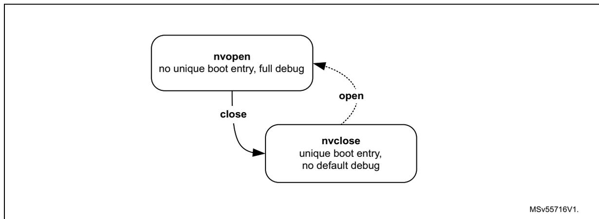
Introduction
Figure 18 shows how embedded flash manages the non-volatile security life cycle of the device.
Figure 18. Life cycle management scheme
graph TD
    nvopen[nvopen
no unique boot entry, full debug] -- close --> nvclose[nvclose
unique boot entry, no default debug]
    nvclose -.->|open| nvopen
    MSv55716V1
Table 35 details the non-volatile security lifecycle NVSTATE and its effects on the product.
Table 35. Flash security lifecycle definition
| NVSTATE | Boot address (1) | Debug level | Regression to | Root HUK |
|---|---|---|---|---|
| OPEN | 0x0800 0000 or Bootloader | Unconstrained (2) | n/a | 0x0 |
| CLOSE | 0x1FF0 0000 | Constrained (3) | OPEN | OB Key (ST) |
1. Enforced outside flash.
2. Includes STMicroelectronics engineering test modes. Those are disabled in CLOSE state, by hardware.
3. User can attempt to unlock debug features, if allowed by DEBUG_AUTH option bits.
Flash opening
When requesting a change of NVSTATE to OPEN, writing 0xB4 to FLASH_NVSRR register, flash performs an automatic erase of the following information:
- • The whole user flash (write protected or not)
- • The write protection data in FLASH_WRPSR.
- • The option byte register defining the hide protection area is reset to their default manufacturing values (disabled).
- • The option byte keys, excluding hide protection level 0 keys
- • Root of trust option byte registers: FLASH_ROTSP and FIXEDSP
Note: The FLASH_EPOCHSP setting is kept when opening the flash memory
NVSTATE option change is triggered only after the RAM erase signal has confirmed that Backup RAM and PKA RAM have been successfully erased.
The system flash memory and the read-only region are not affected by flash opening and remain unchanged.
Flash closing
Writing 0x51 to the FLASH_NVSRR register triggers a change of NVSTATE from OPEN to CLOSE, confirmed when NVSTATE=0x51 in FLASH_NVSR register.
5.5.4 Hide protected system flash area
System flash sectors included between 0x1FF0 0000 and SEC_AREA_END addresses can be used to store STMicroelectronics secure firmware install (SFI) code, or the STM32 immutable root of trust code and data, with the associated encrypted keys stored in option byte keys.
Embedded flash system area can only be accessed by Cortex M7 in read or execute. The hide protected area can only be accessed when NVSTATE is CLOSE and when hide protection level in SBS_HDPLSR is 0 or 1 for ST iRoT products (default), or just 0 for OEM iRoT products.
In all other cases one of the following events is triggered:
- • Data read transactions return zero. Data write transactions are ignored. No bus error is generated but an error flag is raised (RDSERR for read, WRPERR for write).
- • Read instruction transactions generate a bus error and the RDSERR error flag is raised.
Embedded flash system area is immutable, that is, it cannot be erased by any application code.
Note: When FLASH transition from CLOSE to OPEN state, embedded flash system area is kept.
5.5.5 Hide protected user flash area
Overview
User flash sectors included between HDP_AREA_START and HDP_AREA_END addresses are used to store the root of trust code and data, with the associated keys stored in embedded flash option byte keys.
Embedded flash hide protected (HDP) user area can only be accessed:
- • by Cortex M7 in read, write or execute
- • according to the conditions defined in following tables. Table 36 concerns STM32H7R parts, or STM32H7S parts with IROT_SELECT different from 0xB4. STM32H7S parts with ST iRoT (IROT_SELECT=0xB4) are described in Table 37 .
Table 36. Boot level and HDP area protections (non STiRoT case)
| Product state | FLASH user options (1) | HDP level (2) to activate protection | Boot address (HDPL) | Comment | ||
|---|---|---|---|---|---|---|
| NV STATE | OEM_PROVD | HDP area in system flash | HDP area in user flash | |||
| Open | OPEN | >1 | User flash or bootloader (HDPL1) | RSS not visible | ||
| Provisioning | CLOSE | not 0xB4 | >0 | >0 | RSS (HDPL0) | Firmware provisioning in user flash, and provisioning of related keys in OBKey area. |
| Closed or Locked | 0xB4 | >1 | Firmware provisioned in user flash. All related OBKeys are also provisioned. | |||
1. In FLASH_NVSR and FLASH_ROTSR registers
2. Level for which hide protection is activated.
Table 37. Boot level and HDP area protections (STiRoT case)
| Product state | FLASH user options (1) | HDP level (2) to activate protection | Boot address (HDPL) | Comment | ||
|---|---|---|---|---|---|---|
| NV STATE | OEM_PROVD | HDP area in system flash | HDP area in user flash | |||
| Open | OPEN | >0 | >2 | User flash (HDPL2) or bootloader (HDPL1) | ST iRoT not visible | |
| Provisioning | CLOSE | not 0xB4 | >1 | >1 | RSS (HDPL0) | OEM uRoT provisioning in user flash, and provisioning of related keys in OBKey area. |
| Closed or Locked | 0xB4 | >2 | OEM uRoT provisioned in user flash. All related OBKeys are also provisioned. | |||
1. In FLASH_NVSR and FLASH_ROTSR registers
2. Level for which hide protection is activated.
For more details on HDPL level following a reset, refer to Section 8: System configuration, boot and security (SBS) .
Note: IROT_SELECT is stored in the FLASH_ROTSR register.
Hide protection area in user flash programming
HDP user flash area is programmed in FLASH_HDPSRP by setting the HDP_AREA_START and HDP_AREA_END so that the END address is strictly higher than the START address.
HDP_AREA_START and HDP_AREA_END are defined with a granularity of 256 bytes. This means that the actual HDP user flash area size (in bytes) is defined by:
As an example, to set the HDP user flash area on the first 8 Kbytes (that is, from address 0x0800 0000 to address 0x0800 1FFF, both included), the embedded flash memory must be configured as follows:
HDP_AREA_START[15:0] = 0x0
HDP_AREA_END[15:0] = 0x001F
The HDP user flash area size defined above is equal to:
The minimum HDP user flash area that can be set is 32 flash words (or 512 bytes). The maximum area is the whole user flash memory bank, configured by setting HDP_AREA_START= HDP_AREA_END.
Note: It is recommended to align the HDP user area size with 8 Kbytes flash sector granularity to always be able to erase non-HDP code and data.
It is possible to disable HDP protections by setting HDP_AREA_END lower than HDP_AREA_START.
Hide protection area in user flash properties
- • Embedded flash hide protected user area can only be accessed in the conditions described in
Overview
. In all other cases one of the following events is triggered:
- – Data read transactions return zero. Data write transactions are ignored. No bus error is generated but an error flag is raised (RDSERR for read, WRPERR for write).
- – Read instruction transactions generate a bus error and the RDSERR error flag is raised.
- • HDP user flash area is erase-protected. As a result:
- – No erase operations to a sector located in this area are possible (including the sector containing the area end address), unless HDPL=0 or 1.
- – In HDPL=2 or 3 the only possibility to fully erase user flash bank is to perform a device opening sequence (see Section 5.5.3 ).
- • Rules to change the HDP user flash area are detailed in Changing option byte words in Section 5.4.3 .
- • When FLASH transition from CLOSE to OPEN state, the whole user flash (hide protected or not) is automatically erased, with the HDP area disabled (see Section 5.5.3 ).
For more information on HDP user flash area errors, refer to Section 5.7: FLASH error management .
5.6 FLASH low-power modes
5.6.1 Introduction
Table 38 summarizes the behavior of the embedded flash memory in microcontroller low-power modes. The embedded flash memory belongs to the Core domain.
Table 38. Effect of low-power modes on the embedded flash memory
| Power mode | Core domain voltage range | Allowed if FLASH busy | FLASH power mode (in Core domain) |
|---|---|---|---|
| System state | |||
| Run | VOS low / high | Yes | Run |
| Stop | SVOS low / high | No | Clock gated or Stopped |
| Standby | Off | No | Off |
When the system state changes, or within a given system state, the embedded flash memory might be subjected to a different voltage supply range (VOS) depending on the application. The procedure to switch the embedded flash memory into various power modes (run, clock gated, stopped, off) is described below.
Note: For more information on microcontroller power states, refer to the Power control section (PWR).
5.6.2 Managing the FLASH domain switching to Stop or Standby
As explained in Table 38 , if the embedded flash memory informs the reset and clock controller (RCC) that it is busy (that is, BUSY, QW, WBNE is set), the microcontroller cannot switch the Core domain to Stop or Standby mode.
Note: CRC_BUSY is not taken into account.
There are two ways to release the embedded flash memory:
- • Reset the WBNE busy flag in the FLASH_SR register by any of the following actions:
- – Complete the write buffer with missing data.
- – Force the write operation without filling-in the missing data, by activating the FW bit in the FLASH_CR register. This forces all missing data “high”.
- – Reset the PG bit in FLASH_CR register. This disables the write buffer and consequently leads to the loss of its content.
- • Poll the QW busy bits in the FLASH_SR register until they are cleared. This indicates that all recorded write, erase and option change operations are complete.
The microcontroller can then switch the domain to Stop or Standby mode.
5.7 FLASH error management
5.7.1 Introduction
The embedded flash memory automatically reports when an error occurs during a read, program or erase operation. A wide range of errors are reported:
- • Write protection error (WRPERRF)
- • Programming sequence error (PGSERRF)
- • Strobe error (STRBERRF)
- • Inconsistency error (INCERRF)
- • Error correction code error (SNECCERRF/DBECCERRF)
- • Read secure error (RDSERRF)
- • CRC read error (CRCRDERRF)
- • Option byte change error (OPTERRF)
- • Key valid error (KVEF)
- • Key transfer error (KTEF)
- • Option byte loading error (OBLERRF)
The application software can individually enable the interrupt for each error, as detailed in Section 5.8: FLASH interrupts .
Note: For some errors, the application software must clear the error flag before attempting a new operation.
Note: General purpose errors (e.g. INCERRF) are taken into account when queues are loaded. Temporal isolation and other protection errors (for example WRPERRF, RDSERRF) are taken into account at FSM level, in front of the flash bank interface controller.
5.7.2 Write protection error (WRPERRF)
When an illegal erase/program operation is attempted to the non-volatile memory, the embedded flash memory sets the write protection error flag WRPERRF in FLASH_ISR register.
An erase operation is rejected and flagged as illegal if it targets one of the following memory areas:
- • a sector belonging to a valid HDP user flash area (even partially), except if HDPL=0 or 1 in SBS_HDPLSR register.
- • a sector write-locked with WRPS
- • the read-only/OTP area
An program operation is ignored and flagged as illegal if it targets one of the following memory areas:
- • a protected user flash sector belonging to a valid HDP user flash area (see Section 5.5.5 )
- • a user sector write-locked with WRPS
- • an OTP block, locked with OTPL
- • a read-only section
- • the system flash memory
- • a reserved area
When the WRPERRF flag is raised, the operation is rejected and nothing is changed. If a write burst operation was ongoing, WRPERRF is raised each time a flash word write operation is processed by the embedded flash memory.
Note: The WRPERRF flag does not block any new erase/program operation.
Not clearing the WRPERRF flag does not generate a programming sequence error (see below).
WRPERRF flag is cleared by setting the corresponding bit in FLASH_ICR register.
If WRPERRIE bit in FLASH_IER register is set, an interrupt is generated when the WRPERRF flag is raised (see Section 5.8: FLASH interrupts for details).
5.7.3 Programming sequence error (PGSERRF)
When the programming sequence is incorrect, the embedded flash memory sets the programming sequence error flag PGSERRF in FLASH_ISR register.
More specifically, the PGSERRF flag is set if one of the conditions below is met:
- • A write operation is requested but the program enable bit (PG or PG_OTP) has not been set in the FLASH_CR register prior to the request. This program enable bit must stay at 1 until write is added to operation queue (QW rises).
- • The inconsistency error (INCERRF) has not been cleared before requesting a new write operation.
When THE PGSERRF flag is raised, the current program operation is aborted and nothing is changed in flash. The corresponding write data buffer is also flushed. If a write burst operation was ongoing, PGSERRF is raised at the end of the burst.
Note: When the PGSERRF flag is raised, there is a risk that the last write operation performed by the application has been lost because of the above protection mechanism. Hence it is recommended to generate interrupts on PGSERRF and verify in the interrupt handler if the last write operation has been successful by reading back the value in the flash memory.
The PGSERRF flag also blocks any new program operation. This means that PGSERRF must be cleared before starting a new program operation.
The PGSERRF flag is cleared by setting the corresponding bit in the FLASH_ICR register.
If the PGSERRIE bit in FLASH_IER register is set, an interrupt is generated when the PGSERRF flag is raised. See Section 5.8: FLASH interrupts for details.
5.7.4 Strobe error (STRBERRF)
When the application software writes several times to the same byte write buffer, the embedded flash memory sets the strobe error flag STRBERRF in the FLASH_ISR register.
When the STRBERRF flag is raised, the current program operation is not aborted and new byte data replaces the old data. The application can ignore the error, proceed with the current write operation and request new write operations. If a write burst was ongoing, STRBERRF is raised at the end of the burst.
The STRBERRF flag is cleared by setting corresponding bit in the FLASH_ICR register.
If the STRBERRIE bit in the FLASH_IER register is set, an interrupt is generated when the STRBERRF flag is raised. See Section 5.8: FLASH interrupts for details.
5.7.5 Inconsistency error (INCERRF)
When a programming inconsistency is detected, the embedded flash memory sets the inconsistency error flag INCERRF in the FLASH_ISR register.
More specifically, the INCERRF flag is set when one of the following conditions is met:
- • A write operation is attempted before completion of the previous write operation, for example:
- – The application software starts a write operation to fill the 128-bit write buffer, but sends a new write burst request to a different flash memory address before the buffer is full.
- – One master starts a write operation, but before the buffer is full, another master starts a new write operation to the same address or to a different address.
- • A wrap burst request issued by a master overlaps two or more 128-bit flash-word addresses, that is, wrap bursts must be done within 128-bit flash-word address boundaries.
Following the sequence below is recommended to avoid losing data when an inconsistency error occurs:
- 1. Execute a handler routine when the INCERRF flag is raised.
- 2. Stop all write requests to embedded flash memory.
- 3. Verify that the write operations that have been requested just before the INCERRF event have been successful by reading back the programmed values from the memory.
- 4. Clear the INCERRF bit in the FLASH_ICR register.
- 5. Restart the write operations where they have been interrupted.
Note: INCERRF flag must be cleared before starting a new write operation, otherwise a sequence error (PGSERRF) is raised.
Any write triggering inconsistency error is discarded by embedded flash memory.
5.7.6 Error correction code error (SNECCERRF/DBECCERRF)
When a single error correction is detected during a read the embedded flash memory sets the single error correction flag SNECCERRF in the FLASH_ISR register.
When two ECC errors are detected during a read, the embedded flash memory sets the double error detection flag DBECCERRF in the FLASH_ISR register.
When the SNECCERRF flag is raised, the corrected read data are returned. Hence the application can ignore the error and request new read operations.
If a read burst operation was ongoing, the SNECCERRF or DBECCERRF flag is raised each time a new data is sent back to the requester through the corresponding system bus.
When the SNECCERRF (or DBECCERRF respectively) flag is raised, the address of the flash word that generated the error is saved in the FLASH_ECCSFAR (or FLASH_ECCDFAR respectively) register. This register is automatically cleared when the associated flag that generated the error is cleared.
Note: In the case of successive single correction (or double detection respectively) errors, only the address corresponding to the first error is stored in the FLASH_ECCSFAR (or FLASH_ECCDFAR respectively) register.
When the DBECCERRF flag is raised reading the user flash memory, a bus error is generated. In the case of successive double error detections, a bus error is generated each time a new data is sent back to the requester through the AXI interface.
Note: It is not mandatory to clear the SNECCERRF or DBECCERRF flags before starting a new read operation.
The SNECCERRF and DBECCERRF flags are cleared by setting corresponding bit in the FLASH_ICR register.
If the SNECCERRIE (or respectively DBECCERRIE) bit in the FLASH_ISR register is set, an interrupt is generated when the SNECCERRF (or respectively DBECCERRF) flag is raised. See Section 5.8: FLASH interrupts for details.
5.7.7 Read secure error (RDSERRF)
When an illegal read or execute operation is attempted to a hide protected area, the embedded flash memory sets the read secure the error flag RDSERRF in the FLASH_ISR register. For more information on illegal access definition, refer to Section 5.5.4: Hide protected system flash area and Section 5.5.5: Hide protected user flash area .
When the RDSERRF flag is raised, the current read operation is aborted and the application can request new read operations. If a read burst was ongoing, RDSERRF is raised each time a data is sent back to the requester through the AXI interface.
Note: The bus error is raised only if the illegal access is due to an instruction fetch.
RDSERRF flag is cleared by setting corresponding bit in the FLASH_ICR register.
If the RDSERRIE bit in the FLASH_IER register is set, an interrupt is generated when the RDSERRF flag is raised (see Section 5.8: FLASH interrupts for details).
5.7.8 CRC read error (CRCRDERRF)
After a CRC computation, the embedded flash memory sets the CRC read error flag CRCERR in the FLASH_ISR register when one or more address belonging to a protected area was read by the CRC module. A protected area corresponds to a valid HDP area in user flash, for which any read is currently illegal (see Section 5.5.5 for details).
The CRCRDERRF flag is raised when the CRCEND bit is set (end of CRC calculation). In this case, it is likely that the CRC result is wrong since illegal read operations to protected areas return null values.
The CRCRDERRF flag is cleared by setting corresponding bit in the FLASH_ICR register.
If the CRCRDERRIE bit in the FLASH_IER register is set, an interrupt is generated when the CRCRDERRF flag is raised together with the CRCEND bit (see Section 5.8: FLASH interrupts for details).
5.7.9 Option byte change error (OPTERRF)
When the embedded flash memory finds an error during an option change operation, it aborts the operation and sets the option byte change the error flag OPTERRF in the FLASH_OPTISR register.
The OPTERRF flag is cleared by setting corresponding bit in the FLASH_OPTICR register.
If the OPTERRIE bit in the FLASH_OPTCR register is set, an interrupt is generated when the OPTERRF flag is raised (see Section 5.8: FLASH interrupts for details).
It is mandatory to clear the OPTERRF flag before starting a new option byte change, or an option byte key programming.
5.7.10 Key valid error (KVEF)
KVEF error flag is set in the FLASH_OPTISR register in two cases:
- • Embedded flash did not find an option byte key that corresponds to the given OBKINDEX[4:0] and the requested HDPL (optionally modified by NEXTKL[1:0]). It can happen for example when requested key has not been provisioned.
- • A double error detection was found when loading the requested option byte key. In this case, if this key is provisioned again the error should disappear.
It is mandatory to clear the KVEF flag before doing any operation on option byte keys because when KVEF is set, writes to the START bit in the FLASH_OBKCR are ignored.
The KVEF flag is cleared by setting corresponding bit in FLASH_OPTICR register.
If the KVEIE bit in the FLASH_OPTCR register is set, an interrupt is generated when the KVEF flag is raised (see Section 5.8: FLASH interrupts for details).
5.7.11 Key transfer error (KTEF)
The KTEF error flag is set in the FLASH_OPTISR register when embedded flash signals an error to the SAES peripheral. This happens when:
- • the key size (128-bit or 256-bit) is not matching between embedded flash OBKSIZE[1:0] and KEYSIZE bit in SAES_CR register.
- • an ECC dual error detection occurred while embedded flash loaded an option byte key for the SAES peripheral. In this case KVEF is also set.
It is mandatory to clear the KTEF flag before doing any operation on option byte keys. Because when KTEF is set write to the START bit in the FLASH_OBKCR is ignored.
The KTEF flag is cleared by setting corresponding bit in the FLASH_OPTICR register.
If the KTEIE bit in the FLASH_OPTCR register is set, an interrupt is generated when the KTEF flag is raised (see Section 5.8: FLASH interrupts for details).
While flash memory loads the option byte key to share with the SAES peripheral no other flash operation should be started until the key is transferred to the SAES. Otherwise the key transfer may fail (BUSY=KEYVALID=0 in the SAES_SR register) or the BUSY bit in the SAES_SR register stays at 1, until IPRST bit is used to clear it.
Note: When KTEF is cleared by the application the error signal to SAES is cleared.
5.7.12 Option byte loading error (OBLERRF)
When the embedded flash memory finds one of the following error during an option byte loading sequence (see Section 5.4.2 ) it sets the option byte change error flag OBLERRF in the FLASH_ISR register.
- • ECC double error detection on one or more option byte (data or metadata)
- • ECC double error detection on one or more option byte key (data or metadata)
In the case of an OBLERRF event the application should verify the correctness of the option byte information described in Section 5.4 .
The OBLERRF flag is cleared by setting the corresponding bit in the FLASH_ICR register. If the OBLERRIE bit in the FLASH_IER register is set, an interrupt is generated when the OBLERRF flag is raised (see Section 5.8: FLASH interrupts for details).
5.7.13 Miscellaneous HardFault errors
The following events generate a bus error on the corresponding bus interface:
- • On the AXI system bus:
- – illegal instruction fetch to HDP protected area because of the lifecycle (e.g. protected system flash when NVSTATE=OPEN).
- • On AHB configuration or system bus:
- – wrong key input to FLASH_KEYR or FLASH_OPTKEYR
- – 8-bit accesses to system AHB interface
5.8 FLASH interrupts
The embedded flash memory can generate a maskable interrupt to signal the following events:
- • Read and write errors (see
Section 5.7: FLASH error management
)
- – Single ECC error correction during read operation
- – Double ECC error detection during read operation
- – Write inconsistency error
- – Bad programming sequence
- – Strobe error during write operations
- – Option change error
- – Option byte keys error
- • Security errors (see
Section 5.7: FLASH error management
)
- – Write protection error
- – Read security error
- – CRC computation on HDP area error
- – Option byte loading error
- – Key valid or key transfer errors
- • Miscellaneous events (described below)
- – End of programming
- – CRC computation complete
These multiple sources are combined into a single interrupt signal, flash_it, which is the only interrupt signal from the embedded flash memory that drives the NVIC (nested vectored interrupt controller).
You can individually enable or disable embedded flash memory interrupt sources by changing the mask bits in the FLASH_IER register. Setting the appropriate mask bit enables the interrupt.
Note: Prior to writing, FLASH_IER register must be unlocked as explained in Section 5.5.1: FLASH configuration protection
Table 39 gives a summary of the available embedded flash memory interrupt features.
Note: Some flags need to be cleared before a new operation is triggered.
Table 39. Flash interrupt request
| Interrupt event | Event flag | Enable control bit | Clear flag to resume operation | Bus error |
|---|---|---|---|---|
| End-of-program event | EOPF | EOPIE | N/A | N/A |
| CRC complete event | CRCENDF | CRCENDIE | N/A | N/A |
| Write protection error | WRPERRF | WRPERRIE | No | No |
| Programming sequence error | PGSERRF | PGSERRIE | Yes | No |
| Strobe error | STRBERRF | STRBERRIE | No | No |
| Inconsistency error | INCERRF | INCERRIE | Yes | No |
| ECC single error correction event | SNECCERRF | SNECCERRIE | No | No |
| ECC double error detection event | DBECCERRF | DBECCERRIE | No | Yes (1) |
| Read secure error | RDSERRF | RDSERRIE | No | No (data) Yes (fetch) |
| CRC error | CRCRDERRF | CRCRDERRIE | No | No |
| Option byte loading error | OBLERRF | OBLERRIE | No | No |
| Option byte change error | OPTERRF (2) | OPTERRIE | No | No |
| Key valid error | KVEF (2) | KVEIE | Yes | No |
| Key transfer error | KTEF (2) | KTEIE | Yes | No |
1. AXI bus only
2. Set in FLASH_OPTISR register, cleared in FLASH_OPTICR register.
The status of the individual maskable interrupt sources described in Table 39 (except for option byte error) can be read from the FLASH_ISR register. They can be cleared by setting the corresponding bit in the FLASH_ICR register.
No unlocking mechanism is required to clear an interrupt.
End-of-program event
Setting the end-of-operation interrupt enable bit (EOPIE) in the FLASH_IER register enables the generation of an interrupt at the end of an erase operation, a program operation or an option byte change. The EOPF bit in the FLASH_ISR register is also set when one of these events occurs.
Setting the EOPF bit in FLASH_ICR register clears the EOPF flag in the FLASH_ISR register.
CRC end of calculation event
Setting the CRC end-of-calculation interrupt enable bit (CRCENDIE) in the FLASH_IER register enables the generation of an interrupt at the end of a CRC operation. The CRCENDF bit in the FLASH_ISR register is also set when this event occurs.
Setting the CRCENDF bit in the FLASH_ICR register clears the CRCENDF flag in the FLASH_ISR register.
5.9 FLASH registers
5.9.1 FLASH access control register (FLASH_ACR)
Address offset: 0x000
Reset value: 0x0000 0013
| 31 | 30 | 29 | 28 | 27 | 26 | 25 | 24 | 23 | 22 | 21 | 20 | 19 | 18 | 17 | 16 |
|---|---|---|---|---|---|---|---|---|---|---|---|---|---|---|---|
| Res. | Res. | Res. | Res. | Res. | Res. | Res. | Res. | Res. | Res. | Res. | Res. | Res. | Res. | Res. | Res. |
| 15 | 14 | 13 | 12 | 11 | 10 | 9 | 8 | 7 | 6 | 5 | 4 | 3 | 2 | 1 | 0 |
| Res. | Res. | Res. | Res. | Res. | Res. | Res. | Res. | Res. | Res. | WRHIGHFREQ [1:0] | |||||
| rw | rw | rw | rw | rw | rw |
Bits 31:6 Reserved, must be kept at reset value.
Bits 5:4 WRHIGHFREQ[1:0] : Flash signal delay
These bits are used to control the delay between non-volatile memory signals during programming operations. Application software has to program them to the correct value depending on the embedded flash memory interface frequency. Refer to Table 29 for details.
Note: Embedded flash does not verify that the configuration is correct.
Bits 3:0 LATENCY[3:0] : Read latency
These bits are used to control the number of wait states used during read operations on both non-volatile memory banks. The application software has to program them to the correct value depending on the embedded flash memory interface frequency and voltage conditions. Refer to Table 29 for details.
0000: zero wait state used to read a word from non-volatile memory
0001: one wait state used to read a word from non-volatile memory
0010: two wait states used to read a word from non-volatile memory
...
0111: seven wait states used to read a word from non-volatile memory
1111: fifteen wait states used to read from non-volatile memory
Note: Embedded flash does not verify that the configuration is correct.
5.9.2 FLASH control key register (FLASH_KEYR)
Address offset: 0x004
Reset value: 0x0000 0000
| 31 | 30 | 29 | 28 | 27 | 26 | 25 | 24 | 23 | 22 | 21 | 20 | 19 | 18 | 17 | 16 |
|---|---|---|---|---|---|---|---|---|---|---|---|---|---|---|---|
| CUKEY[31:16] | |||||||||||||||
| w | w | w | w | w | w | w | w | w | w | w | w | w | w | w | w |
| 15 | 14 | 13 | 12 | 11 | 10 | 9 | 8 | 7 | 6 | 5 | 4 | 3 | 2 | 1 | 0 |
| CUKEY[15:0] | |||||||||||||||
| w | w | w | w | w | w | w | w | w | w | w | w | w | w | w | w |
Bits 31:0 CUKEY[31:0] : Control unlock key
Following values must be written to FLASH_KEYR consecutively to unlock FLASH_CR register:
1st key = 0x4567 0123
2nd key = 0xCDEF 89AB
Reads to this register returns zero. If above sequence is wrong or performed twice, the FLASH_CR register is locked until the next system reset, and access to it generates a bus error.
5.9.3 FLASH control register (FLASH_CR)
Address offset: 0x010
Reset value: 0x0000 0001
When LOCK bit in this register is set writes to all other bits are ignored.
Write access to this register is controlled by FLASH_KEYR.
| 31 | 30 | 29 | 28 | 27 | 26 | 25 | 24 | 23 | 22 | 21 | 20 | 19 | 18 | 17 | 16 |
|---|---|---|---|---|---|---|---|---|---|---|---|---|---|---|---|
| Res. | Res. | Res. | Res. | Res. | Res. | Res. | ALL_BANKS | Res. | Res. | Res. | Res. | Res. | Res. | CRC_EN | PG_OTP |
| rw | rw | rw | |||||||||||||
| 15 | 14 | 13 | 12 | 11 | 10 | 9 | 8 | 7 | 6 | 5 | 4 | 3 | 2 | 1 | 0 |
| Res. | Res. | Res. | Res. | Res. | Res. | Res. | SSN[2:0] | START | FW | BER | SER | PG | LOCK | ||
| rw | rw | rw | rw | rw | rw | rw | rw | rs | |||||||
Bits 31:25 Reserved, must be kept at reset value.
Bit 24 ALL_BANKS : All banks select bit
When this bit is set the erase is done on all flash memory sectors.
ALL_BANKS is used only if a bank erase is required (BER=1). In all other operations, this control bit is ignored.
Bits 23:18 Reserved, must be kept at reset value.
Bit 17 CRC_EN : CRC enable
Setting this bit enables the CRC calculation. CRC_EN does not start CRC calculation but enables CRC configuration through FLASH_CRCCR register.
When CRC calculation is performed it can be disabled by clearing CRC_EN bit. Doing so sets CRCDATA to 0x0, clears CRC configuration and resets the content of FLASH_CRCDATAR register.
Bit 16
PG_OTP
: Program Enable for OTP Area
Set this bit to enable write operations to OTP area.
Bits 15:9 Reserved, must be kept at reset value.
Bits 8:6 SSN[2:0] : Sector erase selection number
These bits are used to select the target sector for an erase operation (they are unused otherwise).
000: Sector 0
001: Sector 1
...
111: Sector 7
Bit 5 START : Erase start control bit
This bit is used to start a sector erase or a bank erase operation. The embedded flash memory resets START when the corresponding operation has been acknowledged. The user application cannot access any embedded flash memory register until the operation is acknowledged.
Bit 4 FW : Force write
This bit forces a write operation even if the write buffer is not full. In this case all bits not written are set by hardware. The embedded flash memory resets FW when the corresponding operation has been acknowledged.
Note: Using a force-write operation prevents the application from updating later the missing bits with something other than 1, because this would likely to lead to a permanent ECC error.
Write forcing is effective only if the write buffer is not empty (in particular, FW does not start several write operations when the force-write operations are performed consecutively).
Bit 3 BER : Bank erase request
Setting this bit requests a bank erase operation (user flash memory only).
0: Bank erase is not requested
1: Bank erase is requested. Actual erase is started setting START bit in this register.
Write protection error is triggered when a bank erase is required and some sectors are protected.
BER has a higher priority than SER: if both are set, the embedded flash memory executes a bank erase.
Bit 2 SER : Sector erase requestSetting this bit requests a sector erase.
0: Sector erase not requested
1: Sector erase requested
Write protection error is triggered when a sector erase is required on at least one protected sector.
BER has a higher priority than SER: if both bits are set, the embedded flash memory executes a bank erase.
Bit 1 PG : Internal buffer control bitSetting this bit enables internal buffer for write operations. This allows preparing program operations even if a sector or bank erase is ongoing. When PG is cleared, the internal buffer is disabled for write operations, and all the data stored in the buffer but not sent to the operation queue are lost.
0: Internal buffer disabled for write operations
1: Internal buffer enabled for write operations
Bit 0 LOCK : Configuration lock bitWhen this bit is set write to all other bits in this register, and to FLASH_IER register, are ignored.
0: FLASH_CR and FLASH_IER registers are unlocked
1: Writes to FLASH_IER, and to other bits than LOCK in FLASH_CR, are ignored
Clearing this bit requires the correct write sequence to FLASH_KEYR register (see this register for details). If a wrong sequence is executed, or if the unlock sequence is performed twice, this bit remains locked until the next system reset.
During the write access to set LOCK bit from 0 to 1, it is possible to change the other bits of this register.
5.9.4 FLASH status register (FLASH_SR)
Address offset: 0x014
Reset value: 0x0000 0000
| 31 | 30 | 29 | 28 | 27 | 26 | 25 | 24 | 23 | 22 | 21 | 20 | 19 | 18 | 17 | 16 |
|---|---|---|---|---|---|---|---|---|---|---|---|---|---|---|---|
| Res. | Res. | Res. | Res. | Res. | Res. | Res. | Res. | Res. | Res. | Res. | Res. | Res. | Res. | Res. | Res. |
| 15 | 14 | 13 | 12 | 11 | 10 | 9 | 8 | 7 | 6 | 5 | 4 | 3 | 2 | 1 | 0 |
| Res. | Res. | Res. | Res. | Res. | Res. | Res. | Res. | Res. | IS_OPTCHANGE | IS_ERASE | IS_PROGRAM | CRC_BUSY | QW | WBNE | BUSY |
| r | r | r | r | r | r | r |
Bits 31:7 Reserved, must be kept at reset value.
Bit 6 IS_OPTCHANGE : Is an option change
This bit is set together with BUSY when an option change operation is ongoing. It is cleared when BUSY is cleared.
This flag can also raise with IS_PROGRAM or IS_ERASE, because a program or erase step is ongoing during option change.
Bit 5 IS_ERASE : Is an erase
This bit is set together with BUSY when an erase operation is ongoing. It is cleared when BUSY is cleared.
This flag can also raise with IS_OPTCHANGE, because an erase operation can happen during an option change.
Bit 4 IS_PROGRAM : Is a program
This bit is set together with BUSY when a program operation is ongoing. It is cleared when BUSY is cleared.
This flag can also raise with IS_OPTCHANGE, because an program operation can happen during an option change.
Bit 3 CRC_BUSY : CRC busy flag
This bit is set when a CRC calculation is ongoing. This bit cannot be forced to 0. The user must wait until the CRC calculation has completed or disable CRC computation using CRC_EN bit in FLASH_CR register.
0: No CRC calculation ongoing
1: CRC calculation ongoing
Bit 2 QW: Wait queue flagThis bit is set when a write, erase or option byte change operation is pending in the command queue buffer. It is not possible to know what type of programming operation is present in the queue.
This flag is reset by hardware when all write, erase or option byte change operations have been executed and thus removed from the waiting queue(s). This bit cannot be forced to 0. It is reset after a deterministic time if no other operations are requested.
0: No write, erase or option byte change operations waiting in the operation queues
1: At least one write, erase or option byte change operation is waiting in the operation queue
Bit 1 WBNE: Write buffer not empty flagThis bit is set when the embedded flash memory is waiting for new data to complete the write buffer. In this state, the write buffer is not empty. WBNE is reset by hardware each time the write buffer is complete or the write buffer is emptied following one of the event below:
- – the application software forces the write operation using FW bit in FLASH_CR
- – the embedded flash memory detects an error that involves data loss
- – the application software has disabled write operations
This bit cannot be forced to 0. To reset it, clear the write buffer by performing any of the above listed actions, or send the missing data.
0: Write buffer empty or full
1: Write buffer waiting data to complete
Bit 0 BUSY: Busy flagThis bit is set when an effective write, erase or option byte change operation is ongoing. It is possible to know what type of operation is being executed reading the flags IS_PROGRAM, IS_ERASE and IS_OPTCHANGE.
BUSY cannot be cleared by application. It is automatically reset by hardware every time a step in a write, erase or option byte change operation completes. It is not recommended to do software polling on BUSY to know when one operation completed because, depending of operation, more pulses are possible for one only operation. For software polling it is therefore better to use QW flag or to check the EOPF flag.
0: No programming, erase or option byte change operation are being executed
1: Programming, erase or option byte change operation are being executed. See flags IS_PROGRAM, IS_ERASE and IS_OPTCHANGE for details.
5.9.5 FLASH interrupt enable register (FLASH_IER)
Address offset: 0x020
Reset value: 0x0000 0000
Writes to this register are ignored if LOCK bit is set in FLASH_CR register.
| 31 | 30 | 29 | 28 | 27 | 26 | 25 | 24 | 23 | 22 | 21 | 20 | 19 | 18 | 17 | 16 |
|---|---|---|---|---|---|---|---|---|---|---|---|---|---|---|---|
| Res. | Res. | Res. | CRCRDERRIE | CRCENDIE | DBECCERRIE | SNECCERRIE | RDSERRIE | Res. | Res. | INCERRIE | OBLERRIE | STRBERRIE | PGSERRIE | WRPERRIE | EOPIE |
| rw | rw | rw | rw | rw | rw | rw | rw | rw | rw | rw | |||||
| 15 | 14 | 13 | 12 | 11 | 10 | 9 | 8 | 7 | 6 | 5 | 4 | 3 | 2 | 1 | 0 |
| Res. | Res. | Res. | Res. | Res. | Res. | Res. | Res. | Res. | Res. | Res. | Res. | Res. | Res. | Res. | Res. |
Bits 31:29 Reserved, must be kept at reset value.
Bit 28 CRCRDERRIE : CRC read error interrupt enable bit
0: No interrupt is generated when CRCRDERRF bit is set in FLASH_ISR register
1: An interrupt is generated when CRCRDERRF bit is set in FLASH_ISR register
Bit 27 CRCENDIE : CRC end of calculation interrupt enable bit
0: No interrupt is generated when CRCEN bit is set in FLASH_ISR register
1: An interrupt is generated when CRCEN bit is set in FLASH_ISR register
Bit 26 DBECCERRIE : ECC double detection error interrupt enable bit
0: No interrupt is generated when DBECCERRF bit is set in FLASH_ISR register
1: An interrupt is generated when DBECCERRF bit is set in FLASH_ISR register
Bit 25 SNECCERRIE : ECC single correction error interrupt enable bit
0: No interrupt is generated when SNECCERRF bit is set in FLASH_ISR register
1: An interrupt is generated when SNECCERRF bit is set in FLASH_ISR register
Bit 24 RDSERRIE : Read security error interrupt enable bit
0: No interrupt is generated when RDSERRF bit is set in FLASH_ISR register
1: An interrupt is generated when RDSERRF bit is set in FLASH_ISR register
Bits 23:22 Reserved, must be kept at reset value.
Bit 21 INCERRIE : Inconsistency error interrupt enable bit
0: No interrupt is generated when INCERRF bit is set in FLASH_ISR register
1: An interrupt is generated when INCERRF bit is set in FLASH_ISR register
Bit 20 OBLERRIE : Option byte loading error interrupt enable bit
0: No interrupt is generated when OBLERRF bit is set in FLASH_ISR register
1: An interrupt is generated when OBLERRF bit is set in FLASH_ISR register
Bit 19 STRBERRIE : Strobe error interrupt enable bit
0: No interrupt is generated when STRBERRF bit is set in FLASH_ISR register
1: An interrupt is generated when STRBERRF bit is set in FLASH_ISR register
Bit 18 PGSERRIE : Programming sequence error interrupt enable bit
0: No interrupt is generated when PGSERRF bit is set in FLASH_ISR register
1: An interrupt is generated when PGSERRF bit is set in FLASH_ISR register
Bit 17 WRPERRIE : Write protection error interrupt enable bit
0: No interrupt is generated when WRPERRF bit is set in FLASH_ISR register
1: An interrupt is generated when WRPERRF bit is set in FLASH_ISR register
Bit 16 EOPIE : End-of-program interrupt control bit
0: No interrupt is generated when OEPF bit is set in FLASH_ISR register
1: An interrupt is generated when OEPF bit is set in FLASH_ISR register
Bits 15:0 Reserved, must be kept at reset value.
5.9.6 FLASH interrupt status register (FLASH_ISR)
Address offset: 0x024
Reset value: 0x0000 0000
| 31 | 30 | 29 | 28 | 27 | 26 | 25 | 24 | 23 | 22 | 21 | 20 | 19 | 18 | 17 | 16 |
|---|---|---|---|---|---|---|---|---|---|---|---|---|---|---|---|
| Res. | Res. | Res. | RCRDERRF | CRCENDF | DBECCERRF | SNECCERRF | RDERRF | Res. | Res. | INCERRF | OBLERRF | STRBERRF | PGSERRF | WRPERRF | EOPF |
| r | r | r | r | r | r | r | r | r | r | r | |||||
| 15 | 14 | 13 | 12 | 11 | 10 | 9 | 8 | 7 | 6 | 5 | 4 | 3 | 2 | 1 | 0 |
| Res. | Res. | Res. | Res. | Res. | Res. | Res. | Res. | Res. | Res. | Res. | Res. | Res. | Res. | Res. | Res. |
Bits 31:29 Reserved, must be kept at reset value.
Bit 28 RCRDERRF : CRC read error flag
This bit is set when a word is found read protected during a CRC operation. An interrupt is generated if CRCRDIE is set. Setting CRCRDERRF bit in FLASH_ISR register clears this bit.
0: No protected area detected inside addresses read by CRC
1: At least one protected area has been detected inside address read by CRC. As a result CRC result is very likely incorrect.
This flag is valid only when CRCEND bit is set.
Bit 27 CRCENDF : CRC end flag
This bit is set when the CRC computation has completed. An interrupt is generated if CRCENDIE is set. It is not necessary to reset CRCEND before restarting CRC computation. Setting CRCENDF bit in FLASH_ISR register clears this bit.
0: CRC computation not complete
1: CRC computation complete
Bit 26 DBECCERRF : ECC double error flag
This bit is set when an ECC double detection error occurs during a read operation. An interrupt is generated if DBECCERRIE is set. Setting DBECCERRF bit in FLASH_ISR register clears this bit.
0: No ECC double detection error occurred
1: ECC double detection error occurred
Bit 25 SNECCERRF: ECC single error flagThis bit is set when an ECC single correction error occurs during a read operation. An interrupt is generated if SNECCERRIE is set. Setting SNECCERRF bit in FLASH_ICR register clears this bit.
0: No ECC single correction error occurred
1: ECC single correction error occurred
Bit 24 RDSERRF: Read security error flagThis bit is set when a read security error occurs (read access to hide protected area with incorrect hide protection level). An interrupt is generated if RDSERRIE is set. Setting RDSERRF bit in FLASH_ICR register clears this bit.
0: No security error occurred
1: A security error occurred
Bits 23:22 Reserved, must be kept at reset value.
Bit 21 INCERRF: Inconsistency error flagThis bit is set when a inconsistency error occurs. An interrupt is generated if INCERRIE is set. Setting INCERRF bit in the FLASH_ICR register clears this bit.
0: No inconsistency error occurred
1: A inconsistency error occurred
Bit 20 OBLERRF: Option byte loading error flagThis bit is set when an error is found during the option byte loading sequence. An interrupt is generated if OBLERRIE is set.
Setting OBLERRF bit in the FLASH_ICR register clears this bit.
0: No error found during option byte loading sequence
1: Some errors found during option byte loading sequence
Bit 19 STRBERRF: Strobe error flagThis bit is set when a strobe error occurs (when the master attempts to write several times the same byte in the write buffer). An interrupt is generated if the STRBERRIE bit is set.
Setting STRBERRF bit in FLASH_ICR register clears this bit.
0: No strobe error occurred
1: Astrobe error occurred
Bit 18 PGSERRF: Programming sequence error flagThis bit is set when a sequence error occurs. An interrupt is generated if the PGSERRIE bit is set. Setting PGSERRF bit in FLASH_ICR register clears this bit.
0: No sequence error occurred
1: Asequence error occurred
Bit 17 WRPERRF: Write protection error flagThis bit is set when a protection error occurs during a program operation. An interrupt is also generated if the WRPERRIE is set. Setting WRPERRF bit in FLASH_ICR register clears this bit.
0: No write protection error occurred
1: A write protection error occurred
Bit 16 EOPF: End-of-program flagThis bit is set when a programming operation completes. An interrupt is generated if the EOPIE is set. It is not necessary to reset EOPF before starting a new operation. Setting EOPF bit in FLASH_ICR register clears this bit.
0: No programming operation completed
1: A programming operation completed
Bits 15:0 Reserved, must be kept at reset value.
5.9.7 FLASH interrupt clear register (FLASH_ICR)
Address offset: 0x028
Reset value: 0x0000 0000
| 31 | 30 | 29 | 28 | 27 | 26 | 25 | 24 | 23 | 22 | 21 | 20 | 19 | 18 | 17 | 16 |
|---|---|---|---|---|---|---|---|---|---|---|---|---|---|---|---|
| Res. | Res. | Res. | RCRDERRF | RCENDF | DBECCERRF | SNECCERRF | RDSERRF | Res. | Res. | INCERRF | OBLERRF | STRBERF | PGSERRF | WRPERRF | EOPF |
| w | w | w | w | w | w | w | w | w | w | w | |||||
| 15 | 14 | 13 | 12 | 11 | 10 | 9 | 8 | 7 | 6 | 5 | 4 | 3 | 2 | 1 | 0 |
| Res. | Res. | Res. | Res. | Res. | Res. | Res. | Res. | Res. | Res. | Res. | Res. | Res. | Res. | Res. | Res. |
Bits 31:29 Reserved, must be kept at reset value.
Bit 28 RCRDERRF : CRC error flag clear
Setting this bit clears RCRDERRF flag in FLASH_ISR register.
Bit 27 RCENDF : CRC end flag clear
Setting this bit clears RCENDF flag in FLASH_ISR register.
Bit 26 DBECCERRF : ECC double error flag clear
Setting this bit clears DBECCERRF flag in FLASH_ISR register. If the SNECCERRF flag of FLASH_ISR register is also cleared, FLASH_ECCFAR register is reset to zero as well.
Bit 25 SNECCERRF : ECC single error flag clear
Setting this bit clears SNECCERRF flag in FLASH_ISR register. If the DBECCERRF flag of FLASH_ISR register is also cleared, FLASH_ECCFAR register is reset to zero as well.
Bit 24 RDSERRF : Read security error flag clear
Setting this bit clears RDSERRF flag in FLASH_ISR register.
Bits 23:22 Reserved, must be kept at reset value.
Bit 21 INCERRF : Inconsistency error flag clear
Setting this bit clears INCERRF flag in FLASH_ISR register.
Bit 20 OBLERRF : Option byte loading error flag clear
Setting this bit clears OBLERRF flag in FLASH_ISR register.
Bit 19 STRBERF : Strobe error flag clear
Setting this bit clears STRBERF flag in FLASH_ISR register.
Bit 18 PGSERRF : Programming sequence error flag clear
Setting this bit clears PGSERRF flag in FLASH_ISR register.
Bit 17 WRPERRF : Write protection error flag clear
Setting this bit clears WRPERRF flag in FLASH_ISR register.
Bit 16 EOPF : End-of-program flag clear
Setting this bit clears EOPF flag in FLASH_ISR register.
Bits 15:0 Reserved, must be kept at reset value.
5.9.8 FLASH CRC control register (FLASH_CRCCR)
Address offset: 0x030
Reset value: 0x001C 0000
Writes to this register are ignored if CRC_EN bit is cleared in FLASH_CR register.
| 31 | 30 | 29 | 28 | 27 | 26 | 25 | 24 | 23 | 22 | 21 | 20 | 19 | 18 | 17 | 16 |
|---|---|---|---|---|---|---|---|---|---|---|---|---|---|---|---|
| Res. | Res. | Res. | Res. | Res. | Res. | Res. | ALL_SECT | Res. | Res. | CRC_BURST[1:0] | Res. | Res. | CLEAN_CRC | START_CRC | Res. |
| r/w | |||||||||||||||
| 15 | 14 | 13 | 12 | 11 | 10 | 9 | 8 | 7 | 6 | 5 | 4 | 3 | 2 | 1 | 0 |
| Res. | Res. | Res. | Res. | CLEAN_SECT | ADD_SECT | CRC_BY_SECT | Res. | Res. | Res. | Res. | Res. | Res. | CRC_SECT[2:0] | Res. | Res. |
| w | w | r/w |
Bits 31:25 Reserved, must be kept at reset value.
Bit 24 ALL_SECT : All sectors selection
When this bit is set all the sectors in user flash are added to list of sectors on which the CRC is to be calculated.
This bit is cleared when CRC computation starts.
Bits 23:22 Reserved, must be kept at reset value.
Bits 21:20 CRC_BURST[1:0] : CRC burst size
CRC_BURST bits set the size of the bursts that are generated by the CRC calculation unit. A flash word is 128-bit.
00: every burst has a size of 4 flash words (64 Bytes)
01: every burst has a size of 16 flash words (256 Bytes)
10: every burst has a size of 64 flash words (1 Kbytes)
11: every burst has a size of 256 flash words (4 Kbytes)
Bits 19:18 Reserved, must be kept at reset value.
Bit 17 CLEAN_CRC : CRC clear bit
Setting CLEAN_CRC to 1 clears the current CRC result stored in the FLASH_CRCDATAR register.
Bit 16 START_CRC : CRC start bit
START_CRC bit triggers a CRC calculation using the current configuration. No CRC calculation can be launched when an option byte change operation is ongoing because all read accesses to embedded flash memory registers are put on hold until the option byte change operation has completed.
This bit is cleared when CRC computation starts.
Bits 15:12 Reserved, must be kept at reset value.
Bit 11 CLEAN_SECT : CRC sector list clear bit
When this bit is set the list of sectors on which the CRC is calculated is cleared.
Bit 10 ADD_SECT : CRC sector select bit
When this bit is set the sector whose number is written in CRC_SECT is added to the list of sectors on which the CRC is calculated.
Bit 9 CRC_BY_SECT : CRC sector mode select bit
When this bit is set the CRC calculation is performed at sector level, on the sectors present in the list of sectors. To add a sector to this list, use ADD_SECT and CRC_SECT bits. To clean the list, use CLEAN_SECT bit.
When CRC_BY_SECT is cleared the CRC calculation is performed on all addresses defined between start and end addresses defined in FLASH_CRCSTARTADDR and FLASH_CRCENDADDR registers.
Bits 8:3 Reserved, must be kept at reset value.
Bits 2:0 CRC_SECT[2:0] : CRC sector number
CRC_SECT is used to select one user flash sectors to be added to the list of sectors on which the CRC is calculated. The CRC can be computed either between two addresses (using registers FLASH_CRCSTARTADDR and FLASH_CRCENDADDR) or on a list of sectors using this register. If this latter option is selected, it is possible to add a sector to the list of sectors by programming the sector number in CRC_SECT and then setting ADD_SECT bit.
The list of sectors can be erased either by setting CLEAN_SECT bit or by disabling the CRC computation.
000: sector 0 for CRC
001: sector 1 for CRC
...
111: sector 7 for CRC
5.9.9 FLASH CRC start address register (FLASH_CRCSTARTADDR)
Address offset: 0x034
Reset value: 0x0000 0000
| 31 | 30 | 29 | 28 | 27 | 26 | 25 | 24 | 23 | 22 | 21 | 20 | 19 | 18 | 17 | 16 |
|---|---|---|---|---|---|---|---|---|---|---|---|---|---|---|---|
| Res. | Res. | Res. | Res. | Res. | Res. | Res. | Res. | Res. | Res. | Res. | Res. | Res. | Res. | Res. | CRC_START_ADDR[10] |
| rw | |||||||||||||||
| 15 | 14 | 13 | 12 | 11 | 10 | 9 | 8 | 7 | 6 | 5 | 4 | 3 | 2 | 1 | 0 |
| CRC_START_ADDR[9:0] | Res. | Res. | Res. | Res. | Res. | Res. | |||||||||
| rw | rw | rw | rw | rw | rw | rw | rw | rw | rw | ||||||
Bits 31:17 Reserved, must be kept at reset value.
Bits 16:6 CRC_START_ADDR[10:0] : CRC start address
This register is used when CRC_BY_SECT is cleared. It must be programmed to the address of the first flash word to use for the CRC calculation, done burst by burst.
CRC computation starts at an address aligned to the burst size defined in CRC_BURST of FLASH_CRCCR register. Hence least significant bits [5:0] of the address are set by hardware to 0 (minimum burst size= 64 bytes).
The address is relative to the flash bank.
Bits 5:0 Reserved, must be kept at reset value.
5.9.10 FLASH CRC end address register (FLASH_CRCEADDR)
Address offset: 0x038
Reset value: 0x0000 0000
| 31 | 30 | 29 | 28 | 27 | 26 | 25 | 24 | 23 | 22 | 21 | 20 | 19 | 18 | 17 | 16 |
|---|---|---|---|---|---|---|---|---|---|---|---|---|---|---|---|
| Res. | Res. | Res. | Res. | Res. | Res. | Res. | Res. | Res. | Res. | Res. | Res. | Res. | Res. | Res. | CRC_END_ADDR[10] |
| rw | |||||||||||||||
| 15 | 14 | 13 | 12 | 11 | 10 | 9 | 8 | 7 | 6 | 5 | 4 | 3 | 2 | 1 | 0 |
| CRC_END_ADDR[9:0] | Res. | Res. | Res. | Res. | Res. | Res. | |||||||||
| rw | rw | rw | rw | rw | rw | rw | rw | rw | rw | ||||||
Bits 31:17 Reserved, must be kept at reset value.
Bits 16:6 CRC_END_ADDR[10:0] : CRC end address
This register is used when CRC_BY_SECT is cleared. It must be programmed to the address of the flash word starting the last burst of the CRC calculation. The burst size is defined in CRC_BURST of FLASH_CRCCR register.
The least significant bits [5:0] of the address are set by hardware to 0 (minimum burst size= 64 bytes). The address is relative to the flash bank.
Bits 5:0 Reserved, must be kept at reset value.
5.9.11 FLASH CRC data register (FLASH_CRCDATAR)
Address offset: 0x03C
Reset value: 0x0000 0000
| 31 | 30 | 29 | 28 | 27 | 26 | 25 | 24 | 23 | 22 | 21 | 20 | 19 | 18 | 17 | 16 |
|---|---|---|---|---|---|---|---|---|---|---|---|---|---|---|---|
| CRC_DATA[31:16] | |||||||||||||||
| r | r | r | r | r | r | r | r | r | r | r | r | r | r | r | r |
| 15 | 14 | 13 | 12 | 11 | 10 | 9 | 8 | 7 | 6 | 5 | 4 | 3 | 2 | 1 | 0 |
| CRC_DATA[15:0] | |||||||||||||||
| r | r | r | r | r | r | r | r | r | r | r | r | r | r | r | r |
Bits 31:0 CRC_DATA[31:0] : CRC result
This bitfield contains the result of the last CRC calculation. The value is valid only when CRC calculation completed (CRCENDF is set in FLASH_ISR register).
CRC_DATA is cleared when CRC_EN is cleared in FLASH_CR register (CRC disabled), or when CLEAN_CRC bit is set in FLASH_CRCCR register.
5.9.12 FLASH ECC single error fail address (FLASH_ECCSFADDR)
Address offset: 0x040
Reset value: 0x0000 0000
| 31 | 30 | 29 | 28 | 27 | 26 | 25 | 24 | 23 | 22 | 21 | 20 | 19 | 18 | 17 | 16 |
| SEC_FADD[31:16] | |||||||||||||||
| r | r | r | r | r | r | r | r | r | r | r | r | r | r | r | r |
| 15 | 14 | 13 | 12 | 11 | 10 | 9 | 8 | 7 | 6 | 5 | 4 | 3 | 2 | 1 | 0 |
| SEC_FADD[15:0] | |||||||||||||||
| r | r | r | r | r | r | r | r | r | r | r | r | r | r | r | r |
Bits 31:0 SEC_FADD[31:0] : ECC single error correction fail address
When a single ECC error correction occurs during a read operation, the SEC_FADD bitfield contains the system bus address that generated the error.
This register is automatically cleared when SNECCERRF flag that generated the error is cleared.
Note that only the first address that generated an ECC single error correction error is saved in this register.
5.9.13 FLASH ECC double error fail address (FLASH_ECCDFADDR)
Address offset: 0x044
Reset value: 0x0000 0000
| 31 | 30 | 29 | 28 | 27 | 26 | 25 | 24 | 23 | 22 | 21 | 20 | 19 | 18 | 17 | 16 |
| DED_FADD[31:16] | |||||||||||||||
| r | r | r | r | r | r | r | r | r | r | r | r | r | r | r | r |
| 15 | 14 | 13 | 12 | 11 | 10 | 9 | 8 | 7 | 6 | 5 | 4 | 3 | 2 | 1 | 0 |
| DED_FADD[15:0] | |||||||||||||||
| r | r | r | r | r | r | r | r | r | r | r | r | r | r | r | r |
Bits 31:0 DED_FADD[31:0] : ECC double error detection fail address
When a double ECC detection occurs during a read operation, the DED_FADD bitfield contains the system bus address that generated the error.
This register is automatically cleared when the DBECCERRF flag that generated the error is cleared.
Note that only the first address that generated an ECC double error detection error is saved in this register.
5.9.14 FLASH options key register (FLASH_OPTKEYR)
Address offset: 0x100
Reset value: 0x0000 0000

| 31 | 30 | 29 | 28 | 27 | 26 | 25 | 24 | 23 | 22 | 21 | 20 | 19 | 18 | 17 | 16 |
| OCUKEY[31:16] | |||||||||||||||
| w | w | w | w | w | w | w | w | w | w | w | w | w | w | w | w |
| 15 | 14 | 13 | 12 | 11 | 10 | 9 | 8 | 7 | 6 | 5 | 4 | 3 | 2 | 1 | 0 |
| OCUKEY[15:0] | |||||||||||||||
| w | w | w | w | w | w | w | w | w | w | w | w | w | w | w | w |
Bits 31:0 OCUKEY[31:0] : Options configuration unlock key
Following values must be written to FLASH_OPTKEYR consecutively to unlock FLASH_OPTCR register:
1st key = 0x0819 2A3B
2nd key = 0x4C5D 6E7F
Reads to this register returns zero. If above sequence is performed twice locks up the corresponding register/bit until the next system reset, and generates a bus error.
5.9.15 FLASH options control register (FLASH_OPTCR)
Address offset: 0x104
Reset value: 0xX000 0001
When OPTLOCK bit in this register is set writes to all other bits are ignored.
Write access to this register is controlled by FLASH_OPTKEYR register.
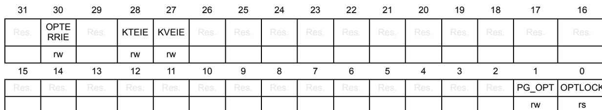
| 31 | 30 | 29 | 28 | 27 | 26 | 25 | 24 | 23 | 22 | 21 | 20 | 19 | 18 | 17 | 16 |
| Res. | OPTE RRIE | Res. | KTEIE | KVEIE | Res. | Res. | Res. | Res. | Res. | Res. | Res. | Res. | Res. | Res. | Res. |
| rw | rw | rw | |||||||||||||
| 15 | 14 | 13 | 12 | 11 | 10 | 9 | 8 | 7 | 6 | 5 | 4 | 3 | 2 | 1 | 0 |
| Res. | Res. | Res. | Res. | Res. | Res. | Res. | Res. | Res. | Res. | Res. | Res. | Res. | Res. | PG_OPT | OPTLOCK |
| rw | rs |
Bit 31 Reserved, must be kept at reset value.
Bit 30 OPTERRIE : Option byte change error interrupt enable bit
This bit controls if an interrupt has to be generated when an error occurs during an option byte change.
0: no interrupt is generated when an error occurs during an option byte change
1: an interrupt is generated when an error occurs during an option byte change.
Bit 29 Reserved, must be kept at reset value.
Bit 28 KTEIE : Key transfer error interrupt enable bit
This bit controls if an interrupt has to be generated when KTEF is set in FLASH_OPTISR.
0: no interrupt is generated when a key transfer error occurs
1: an interrupt is generated when a key transfer error occurs
Bit 27 KVEIE : Key valid error interrupt enable bit
This bit controls if an interrupt has to be generated when KVEF is set in FLASH_OPTISR.
0: no interrupt is generated when a key valid error occurs
1: an interrupt is generated when a key valid error occurs
Bits 26:2 Reserved, must be kept at reset value.
Bit 1 PG_OPT : Program options
0: Update operations to user option bytes and option byte keys do not start
1: Write operation to user option bytes and option byte keys is enabled
Bit 0 OPTLOCK : Options lock
When this bit is set write to all other bits in this register, and write to OTP words, option bytes and option bytes keys control registers, are ignored.
0: OTP words, FLASH_OPTCR, FLASH_OBKCR and FLASH_xxSRP registers are unlocked
1: Writes to OTP words, FLASH_OBKCR, FLASH_xxSRP and to other bits than OPTLOCK in FLASH_OPTCR, are ignored
Clearing this bit requires the correct write sequence to FLASH_OPTKEYR register (see this register for details). If a wrong sequence is executed, or the unlock sequence is performed twice, this bit remains locked until next system reset.
During the write access to set LOCK bit from 0 to 1, it is possible to change the other bits of this register.
5.9.16 FLASH options interrupt status register (FLASH_OPTISR)
Address offset: 0x108
Reset value: 0xXXXX XXXX
| 31 | 30 | 29 | 28 | 27 | 26 | 25 | 24 | 23 | 22 | 21 | 20 | 19 | 18 | 17 | 16 |
|---|---|---|---|---|---|---|---|---|---|---|---|---|---|---|---|
| Res. | OPTER RF | Res. | KTEF | KVEF | Res. | Res. | Res. | Res. | Res. | Res. | Res. | Res. | Res. | Res. | Res. |
| r | r | r | |||||||||||||
| 15 | 14 | 13 | 12 | 11 | 10 | 9 | 8 | 7 | 6 | 5 | 4 | 3 | 2 | 1 | 0 |
| Res. | Res. | Res. | Res. | Res. | Res. | Res. | Res. | Res. | Res. | Res. | Res. | Res. | Res. | Res. | Res. |
Bit 31 Reserved, must be kept at reset value.
Bit 30 OPTERRF : Option byte change error flag
When OPTERRF is set, the option byte change operation did not successfully complete. An interrupt is generated when this flag is raised if the OPTERRIE bit of FLASH_OPTCR register is set. Setting OPTERRF of register FLASH_OPTICR clears this bit.
0: No option byte change errors occurred
1: One or more errors occurred during an option byte change operation.
Bit 29 Reserved, must be kept at reset value.
Bit 28 KTEF : Key transfer error flag
This bit is set when embedded flash signals an error to the SAES peripheral. It happens when the key size (128-bit or 256-bit) is not matching between embedded flash OBKSIZE[1:0] and KEYSIZE bit in SAES_CR register. It also happens when an ECC dual error detection occurred while embedded flash loaded an option byte key for the SAES peripheral.
When KTEF is set write to START bit in FLASH_OBKCR is ignored.
An interrupt is generated when this flag is raised if the KTEIE bit of FLASH_OPTCR register is set. Setting KTEF bit of register FLASH_OPTICR clears this bit.
Bit 27 KVEF : Key valid error flag
This bit is set when loading an unknown or corrupted option byte key. More specifically:
- – Embedded flash did not find an option byte key that corresponds to the given OBKINDEX[4:0] and the requested HDPL (optionally modified by NEXTKL[1:0]). It can happen for example when requested key has not been provisioned.
- – A double error detection was found when loading the requested option byte key. In this case, if this key is provisioned again the error should disappear.
When KVEF is set write to START bit in FLASH_OBKCR is ignored.
An interrupt is generated when this flag is raised if the KVEIE bit of FLASH_OPTCR register is set. Setting KVEF bit of register FLASH_OPTICR clears this bit.
Bits 26:0 Reserved, must be kept at reset value.
5.9.17 FLASH options interrupt clear register (FLASH_OPTICR)
Address offset: 0x10C
Reset value: 0xXXXX XXXX
| 31 | 30 | 29 | 28 | 27 | 26 | 25 | 24 | 23 | 22 | 21 | 20 | 19 | 18 | 17 | 16 |
|---|---|---|---|---|---|---|---|---|---|---|---|---|---|---|---|
| Res. | OPTERRF | Res. | KTEF | KVEF | Res. | Res. | Res. | Res. | Res. | Res. | Res. | Res. | Res. | Res. | Res. |
| w | w | w | |||||||||||||
| 15 | 14 | 13 | 12 | 11 | 10 | 9 | 8 | 7 | 6 | 5 | 4 | 3 | 2 | 1 | 0 |
| Res. | Res. | Res. | Res. | Res. | Res. | Res. | Res. | Res. | Res. | Res. | Res. | Res. | Res. | Res. | Res. |
Bit 31 Reserved, must be kept at reset value.
Bit 30 OPTERRF : Option byte change error flag
Set this bit to clear OPTERRF flag in FLASH_OPTISR register.
Bit 29 Reserved, must be kept at reset value.
Bit 28 KTEF : key transfer error flag
Set this bit to clear KTEF flag in FLASH_OPTISR register.
Bit 27 KVEF : key valid error flag
Set this bit to clear KVEF flag in FLASH_OPTISR register.
Bits 26:0 Reserved, must be kept at reset value.
5.9.18 FLASH option byte key control register (FLASH_OBKCR)
Address offset: 0x110
Reset value: 0x0000 0C00
| 31 | 30 | 29 | 28 | 27 | 26 | 25 | 24 | 23 | 22 | 21 | 20 | 19 | 18 | 17 | 16 |
|---|---|---|---|---|---|---|---|---|---|---|---|---|---|---|---|
| Res. | Res. | Res. | Res. | Res. | Res. | Res. | Res. | Res. | Res. | Res. | Res. | Res. | Res. | Res. | Res. |
| 15 | 14 | 13 | 12 | 11 | 10 | 9 | 8 | 7 | 6 | 5 | 4 | 3 | 2 | 1 | 0 |
| KEYSTART | KEYPROG | Res. | Res. | OBKSIZE[1:0] | NEXTKL[1:0] | Res. | Res. | Res. | OBKINDEX[4:0] | ||||||
| rw | rw | rw | rw | rw | rw | rw | rw | rw | rw | rw | |||||
Bits 31:16 Reserved, must be kept at reset value.
Bit 15 KEYSTART : Key option start
This bit is used to start the option byte key operation defined by the PROG bit.
The embedded flash memory resets START when the corresponding operation has been acknowledged.
Bit 14 KEYPROG : Key program
This bit must be set to write option byte keys (keys are read otherwise).
0: Read key. Result of the operation is stored in FLASH_OBKDRx registers, if applicable.
1: Program key if PG_OPT is set in FLASH_OPTCR register, and KDREF flag is cleared in FLASH_OPTISR register. Correct key information must be stored in FLASH_OBKDRx register before setting PROG and START bits.
Bits 13:12 Reserved, must be kept at reset value.
Bits 11:10 OBKSIZE[1:0] : Option byte key size
Application must use this bitfield to specify how many bits must be used for the new key. Embedded flash ignores OBKSIZE during read of option keys because size is stored with the key.
00: Key size is 32 bits
01: Key size is 64 bits
10: Key size is 128 bits
11: Key size is 256 bits
Bits 9:8 NEXTKL[1:0] : Next key level
00: OBKINDEX represents the index of the option byte key stored for the hide protection level indicated in SBS_HDPLSR.
01: OBKINDEX represents the index of the option byte key stored for the hide protection level indicated in SBS_HDPLSR plus one (e.g. if HDPL=1 in SBS_HDPLR the key of level 2 is selected).
10 or 11: reserved
Bits 7:5 Reserved, must be kept at reset value.
Bits 4:0 OBKINDEX[4:0] : Option byte key index
This bitfield represents the index of the option byte key in a given hide protection level.
Reading keys with index lower than 8, the value is not available in OBKDRx registers. It is instead sent directly to SAES peripheral. All other keys can be read using OBKDRx registers.
Up to 32 256-bit keys can be provisioned per hide protection level (0, 1 or 2).
For keys larger than 256 bits, several indexes must be used.
5.9.19 FLASH option bytes key data register x (FLASH_OBKDRx)
Address offset: 0x118 + 0x4 * x (x=0 to 7)
Reset value: 0x0000 0000
Writes are ignored if KDREF is set in FLASH_OPTISR register.
| 31 | 30 | 29 | 28 | 27 | 26 | 25 | 24 | 23 | 22 | 21 | 20 | 19 | 18 | 17 | 16 |
|---|---|---|---|---|---|---|---|---|---|---|---|---|---|---|---|
| OBKDATA[31:16] | |||||||||||||||
| rw | rw | rw | rw | rw | rw | rw | rw | rw | rw | rw | rw | rw | rw | rw | rw |
| 15 | 14 | 13 | 12 | 11 | 10 | 9 | 8 | 7 | 6 | 5 | 4 | 3 | 2 | 1 | 0 |
| OBKDATA[15:0] | |||||||||||||||
| rw | rw | rw | rw | rw | rw | rw | rw | rw | rw | rw | rw | rw | rw | rw | rw |
Bits 31:0 OBKDATA[31:0] : option byte key data, bits [31+x:0+x]
Data register used in conjunction with FLASH_OBKCR register.
Reading this register (read value once), or incrementing HDPL value in SBS peripheral automatically clears OBKDATA to 0x0. Writing this register prevents reading OBKDATA until option byte key programming sequence is completed.
5.9.20 FLASH non-volatile status register (FLASH_NVSR)
Address offset: 0x200
Reset value: 0x0000 XXXX
This read-only register reflects the current values of corresponding option bits.
| 31 | 30 | 29 | 28 | 27 | 26 | 25 | 24 | 23 | 22 | 21 | 20 | 19 | 18 | 17 | 16 |
|---|---|---|---|---|---|---|---|---|---|---|---|---|---|---|---|
| Res. | Res. | Res. | Res. | Res. | Res. | Res. | Res. | Res. | Res. | Res. | Res. | Res. | Res. | Res. | Res. |
| 15 | 14 | 13 | 12 | 11 | 10 | 9 | 8 | 7 | 6 | 5 | 4 | 3 | 2 | 1 | 0 |
| Res. | Res. | Res. | Res. | Res. | Res. | Res. | Res. | NVSTATE[7:0] | |||||||
| r | r | r | r | r | r | r | r | ||||||||
Bits 31:8 Reserved, must be kept at reset value.
Bits 7:0 NVSTATE[7:0] : Non-volatile state
0xB4: OPEN device
0x51: CLOSED device
Others: invalid configuration.
5.9.21 FLASH security status register programming (FLASH_NVSRP)
Address offset: 0x204
Reset value: 0x0000 XXXX (same as FLASH_NVSR)
Writes to this register are ignored if PG_OPT bit is cleared in FLASH_OPTCR register, or if BUSY and IS_OPTCHANGE bits are set in FLASH_SR register.
Write are ignored if HDPL is different from 0 or 1 in SBS_HDPLSR register.
| 31 | 30 | 29 | 28 | 27 | 26 | 25 | 24 | 23 | 22 | 21 | 20 | 19 | 18 | 17 | 16 |
|---|---|---|---|---|---|---|---|---|---|---|---|---|---|---|---|
| Res. | Res. | Res. | Res. | Res. | Res. | Res. | Res. | Res. | Res. | Res. | Res. | Res. | Res. | Res. | Res. |
| 15 | 14 | 13 | 12 | 11 | 10 | 9 | 8 | 7 | 6 | 5 | 4 | 3 | 2 | 1 | 0 |
| Res. | Res. | Res. | Res. | Res. | Res. | Res. | Res. | NVSTATE[7:0] | |||||||
| rw | rw | rw | rw | rw | rw | rw | rw | ||||||||
Bits 31:8 Reserved, must be kept at reset value.
Bits 7:0 NVSTATE[7:0] : Non-volatile state programming
Write to change corresponding bits in FLASH_NVSR register:
0xB4: OPEN
0x51: CLOSE
Actual option byte change from close to open is triggered only after memory clear hardware process is confirmed. When NVSTATE=0xB4 (resp. 0x51) writing any other value than 0x51 (resp. 0xB4) triggers an option byte change error (OPTERRF).
5.9.22 FLASH RoT status register (FLASH_ROTSR)
Address offset: 0x208
Reset value: 0x0000 XXXX
This read-only register reflects the current values of corresponding option bits.
| 31 | 30 | 29 | 28 | 27 | 26 | 25 | 24 | 23 | 22 | 21 | 20 | 19 | 18 | 17 | 16 |
|---|---|---|---|---|---|---|---|---|---|---|---|---|---|---|---|
| IROT_SELECT[7:0] | Res. | Res. | Res. | Res. | Res. | Res. | Res. | Res. | |||||||
| r | r | r | r | r | r | r | r | ||||||||
| 15 | 14 | 13 | 12 | 11 | 10 | 9 | 8 | 7 | 6 | 5 | 4 | 3 | 2 | 1 | 0 |
| DBG_AUTH[7:0] | OEM_PROVD[7:0] | ||||||||||||||
| r | r | r | r | r | r | r | r | r | r | r | r | r | r | r | r |
Bits 31:24 IROT_SELECT[7:0] : iRoT selection
This option is ignored for STM32H7R device's (user firmware is always selected).
For STM32H7S devices there are two options:
0xB4: ST iRoT is selected at boot
0x6A (default): OEM iRoT is selected at boot.
Bits 23:16 Reserved, must be kept at reset value.
Bits 15:8 DBG_AUTH[7:0] : Debug authentication method
0xB4: Locked device (no debug allowed)
0x51: Authentication method using ECDSA signature (NIST P256)
0x8A: Authentication method using password
Others: no authentication method selected (different to 0xB4, 0x51, 0x8A).
Bits 7:0 OEM_PROVD[7:0] : OEM provisioned device
0xB4: Device has been provisioned by the OEM
Others: device is not provisioned by the OEM.
5.9.23 FLASH RoT status register programming (FLASH_ROTSRP)
Address offset: 0x20C
Reset value: 0x0000 XXXX (same as FLASH_ROTSR)
Writes to this register are ignored if PG_OPT bit is cleared in FLASH_OPTCR register, or if BUSY and IS_OPTCHANGE bits are set in FLASH_SR.
Writes are ignored if HDPL is different from 0 in SBS_HDPLSR register.
| 31 | 30 | 29 | 28 | 27 | 26 | 25 | 24 | 23 | 22 | 21 | 20 | 19 | 18 | 17 | 16 |
|---|---|---|---|---|---|---|---|---|---|---|---|---|---|---|---|
| IROT_SELECT[7:0] | Res. | Res. | Res. | Res. | Res. | Res. | Res. | Res. | |||||||
| rw | rw | rw | rw | rw | rw | rw | rw | ||||||||
| 15 | 14 | 13 | 12 | 11 | 10 | 9 | 8 | 7 | 6 | 5 | 4 | 3 | 2 | 1 | 0 |
| DBG_AUTH[7:0] | OEM_PROVD[7:0] | ||||||||||||||
| rw | rw | rw | rw | rw | rw | rw | rw | rw | rw | rw | rw | rw | rw | rw | rw |
Bits 31:24 IROT_SELECT[7:0] : iRoT selection
This option is ignored for STM32H7R devices.
Write to change corresponding bits in FLASH_ROTSR register.
Bits 23:16 Reserved, must be kept at reset value.
Bits 15:8 DBG_AUTH[7:0] : Debug authentication method programming
Write to change corresponding bits in FLASH_ROTSR register.
Bits 7:0 OEM_PROVD[7:0] : OEM provisioned device
Write to change corresponding bits in FLASH_ROTSR register..
5.9.24 FLASH OTP lock status register (FLASH_OTPLSR)
Address offset: 0x210
Reset value: 0x0000 XXXX
| 31 | 30 | 29 | 28 | 27 | 26 | 25 | 24 | 23 | 22 | 21 | 20 | 19 | 18 | 17 | 16 |
|---|---|---|---|---|---|---|---|---|---|---|---|---|---|---|---|
| Res. | Res. | Res. | Res. | Res. | Res. | Res. | Res. | Res. | Res. | Res. | Res. | Res. | Res. | Res. | Res. |
| 15 | 14 | 13 | 12 | 11 | 10 | 9 | 8 | 7 | 6 | 5 | 4 | 3 | 2 | 1 | 0 |
| OTPL[15:0] | |||||||||||||||
| r | r | r | r | r | r | r | r | r | r | r | r | r | r | r | r |
Bits 31:16 Reserved, must be kept at reset value.
Bits 15:0 OTPL[15:0] : OTP lock n (n=0 to 15)
Block n corresponds to OTP 16-bit word 32 × n to 32 × n + 31.
OTPL[n] = 1 indicates that all OTP 16-bit words in OTP Block n are locked and can no longer be programmed.
OTPL[n] = 0 indicates that all OTP 16-bit words in OTP Block n are not locked and can still be modified.
5.9.25 FLASH OTP lock status register programming (FLASH_OTPLSRP)
Address offset: 0x214
Reset value: 0x0000 XXXX (same as for FLASH_OTPLSR)
Writes to this register are ignored if PG_OPT bit is cleared in FLASH_OPTCR register, or if BUSY and IS_OPTCHANGE bits are set in FLASH_SR.
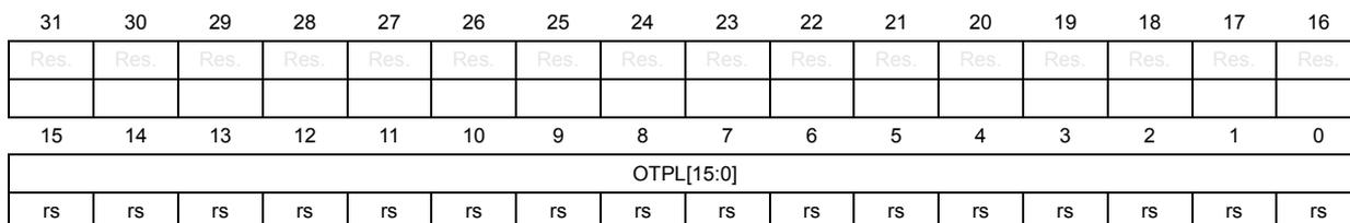
| 31 | 30 | 29 | 28 | 27 | 26 | 25 | 24 | 23 | 22 | 21 | 20 | 19 | 18 | 17 | 16 |
| Res. | Res. | Res. | Res. | Res. | Res. | Res. | Res. | Res. | Res. | Res. | Res. | Res. | Res. | Res. | Res. |
| 15 | 14 | 13 | 12 | 11 | 10 | 9 | 8 | 7 | 6 | 5 | 4 | 3 | 2 | 1 | 0 |
| OTPL[15:0] | |||||||||||||||
| rs | rs | rs | rs | rs | rs | rs | rs | rs | rs | rs | rs | rs | rs | rs | rs |
Bits 31:16 Reserved, must be kept at reset value.
Bits 15:0 OTPL[15:0] : OTP lock n programming (n=0 to 15)
Write to change corresponding option byte bit in FLASH_OTPLSR.
OTPL bits can be only be set, not cleared.
5.9.26 FLASH write protection status register (FLASH_WRPSR)
Address offset: 0x218
Reset value: 0x0000 XXXX
This read-only register reflects the current values of corresponding option bits.
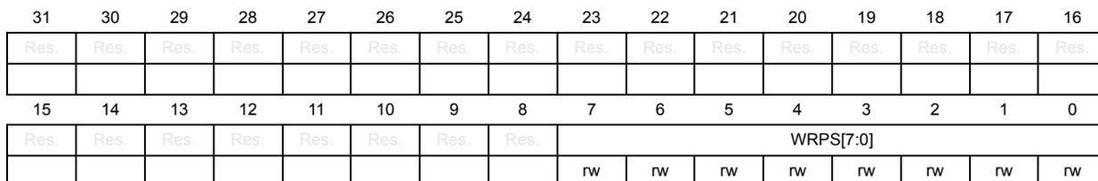
| 31 | 30 | 29 | 28 | 27 | 26 | 25 | 24 | 23 | 22 | 21 | 20 | 19 | 18 | 17 | 16 |
| Res. | Res. | Res. | Res. | Res. | Res. | Res. | Res. | Res. | Res. | Res. | Res. | Res. | Res. | Res. | Res. |
| 15 | 14 | 13 | 12 | 11 | 10 | 9 | 8 | 7 | 6 | 5 | 4 | 3 | 2 | 1 | 0 |
| Res. | Res. | Res. | Res. | Res. | Res. | Res. | Res. | WRPS[7:0] | |||||||
| rw | rw | rw | rw | rw | rw | rw | rw | ||||||||
Bits 31:8 Reserved, must be kept at reset value.
Bits 7:0 WRPS[7:0] : Write protection for sector n (n=0 to 7)
This bit reflects the write protection status of user flash sector n
0: sector n is write protected
1: sector n is not write protected
5.9.27 FLASH write protection status register programming (FLASH_WRPSRP)
Address offset: 0x21C
Reset value: 0x0000 XXXX
Writes to this register are ignored if PG_OPT bit is cleared in FLASH_OPTCR register, or if BUSY and IS_OPTCHANGE bits are set in FLASH_SR.
Writes are ignored if HDPL is different from 0 or 1 in SBS_HDPLSR register.
(The reset value is the same as for FLASH_WRPSR)
| 31 | 30 | 29 | 28 | 27 | 26 | 25 | 24 | 23 | 22 | 21 | 20 | 19 | 18 | 17 | 16 |
|---|---|---|---|---|---|---|---|---|---|---|---|---|---|---|---|
| Res. | Res. | Res. | Res. | Res. | Res. | Res. | Res. | Res. | Res. | Res. | Res. | Res. | Res. | Res. | Res. |
| 15 | 14 | 13 | 12 | 11 | 10 | 9 | 8 | 7 | 6 | 5 | 4 | 3 | 2 | 1 | 0 |
| Res. | Res. | Res. | Res. | Res. | Res. | Res. | Res. | WRPS[7:0] | |||||||
| rw | rw | rw | rw | rw | rw | rw | rw | ||||||||
Bits 31:8 Reserved, must be kept at reset value.
Bits 7:0 WRPS[7:0] : Write protection for sector n programming (n=0 to 7)
Write to change corresponding bit in FLASH_WRPSR
5.9.28 FLASH hide protection status register (FLASH_HDPSR)
Address offset: 0x230
Reset value: 0x0XXX 0000
This read-only register reflects the current values of corresponding option bits.
| 31 | 30 | 29 | 28 | 27 | 26 | 25 | 24 | 23 | 22 | 21 | 20 | 19 | 18 | 17 | 16 |
|---|---|---|---|---|---|---|---|---|---|---|---|---|---|---|---|
| Res. | Res. | Res. | Res. | Res. | Res. | Res. | HDP_AREA_END[8:0] | ||||||||
| r | r | r | r | r | r | r | r | r | |||||||
| 15 | 14 | 13 | 12 | 11 | 10 | 9 | 8 | 7 | 6 | 5 | 4 | 3 | 2 | 1 | 0 |
| Res. | Res. | Res. | Res. | Res. | Res. | Res. | HDP_AREA_START[8:0] | ||||||||
| r | r | r | r | r | r | r | r | r | |||||||
Bits 31:25 Reserved, must be kept at reset value.
Bits 24:16 HDP_AREA_END[8:0] : Hide protection user flash area end
This option sets the end address that contains the last 256-byte block of the hide protection (HDP) area in user flash area.
If HDP_AREA_END=HDP_AREA_START all the sectors are protected.
If HDP_AREA_END<HDP_AREA_START no sectors are protected.
Bits 15:9 Reserved, must be kept at reset value.
Bits 8:0 HDP_AREA_START[8:0] : Hide protection user flash area start
This option sets the start address that contains the first 256-byte block of the hide protection (HDP) area in user flash area.
If HDP_AREA_END=HDP_AREA_START all the sectors are protected.
If HDP_AREA_END<HDP_AREA_START no sectors are protected.
5.9.29 FLASH hide protection status register programming (FLASH_HDPSRP)
Address offset: 0x234
Reset value: 0x0XXX 0000
Writes to this register are ignored if PG_OPT bit is cleared in FLASH_OCR register, or if BUSY and IS_OPTCHANGE bits are set in FLASH_SR.
Write are ignored if HDPL is different from 0 or 1 in SBS_HDPLSR register.
(The reset value is the same as for FLASH_HDPSR.)
| 31 | 30 | 29 | 28 | 27 | 26 | 25 | 24 | 23 | 22 | 21 | 20 | 19 | 18 | 17 | 16 |
|---|---|---|---|---|---|---|---|---|---|---|---|---|---|---|---|
| Res. | Res. | Res. | Res. | Res. | Res. | Res. | HDP_AREA_END[8:0] | ||||||||
| rw | rw | rw | rw | rw | rw | rw | rw | rw | |||||||
| 15 | 14 | 13 | 12 | 11 | 10 | 9 | 8 | 7 | 6 | 5 | 4 | 3 | 2 | 1 | 0 |
| Res. | Res. | Res. | Res. | Res. | Res. | Res. | HDP_AREA_START[8:0] | ||||||||
| rw | rw | rw | rw | rw | rw | rw | rw | rw | |||||||
Bits 31:25 Reserved, must be kept at reset value.
Bits 24:16 HDP_AREA_END[8:0] : Hide protection user flash area end programming
Write to change corresponding option byte bits in FLASH_HDPSR.
If HDP_AREA_END=HDP_AREA_START all the sectors are protected.
If HDP_AREA_END<HDP_AREA_START no sectors are protected.
Bits 15:9 Reserved, must be kept at reset value.
Bits 8:0 HDP_AREA_START[8:0] : Hide protection user flash area start programming
Write to change corresponding option byte bits in FLASH_HDPSR.
If HDP_AREA_END=HDP_AREA_START all the sectors are protected.
If HDP_AREA_END<HDP_AREA_START no sectors are protected.
5.9.30 FLASH epoch status register (FLASH_EPOCHSR)
Address offset: 0x250
Reset value: 0x0000 XXXX
This read-only register reflects the current values of corresponding option bits.
| 31 | 30 | 29 | 28 | 27 | 26 | 25 | 24 | 23 | 22 | 21 | 20 | 19 | 18 | 17 | 16 |
|---|---|---|---|---|---|---|---|---|---|---|---|---|---|---|---|
| Res. | Res. | Res. | Res. | Res. | Res. | Res. | Res. | EPOCH[23:16] | |||||||
| r | r | r | r | r | r | r | r | ||||||||
| 15 | 14 | 13 | 12 | 11 | 10 | 9 | 8 | 7 | 6 | 5 | 4 | 3 | 2 | 1 | 0 |
| EPOCH[15:0] | |||||||||||||||
| r | r | r | r | r | r | r | r | r | r | r | r | r | r | r | r |
Bits 31:24 Reserved, must be kept at reset value.
Bits 23:0 EPOCH[23:0] : Epoch
This value is distributed by hardware to the SAES peripheral.
5.9.31 FLASH RoT status register programming (FLASH_EPOCHSRP)
Address offset: 0x254
Reset value: 0x0000 XXXX
Writes to this register are ignored if PG_OPT bit is cleared in FLASH_OPTCR register, or if BUSY and IS_OPTCHANGE bits are set in FLASH_SR.
Writes are ignored if HDPL is different from 0 in SBS_HDPLSR register.
(The reset value is the same as for FLASH_EPOCHSR.)
| 31 | 30 | 29 | 28 | 27 | 26 | 25 | 24 | 23 | 22 | 21 | 20 | 19 | 18 | 17 | 16 |
|---|---|---|---|---|---|---|---|---|---|---|---|---|---|---|---|
| Res. | Res. | Res. | Res. | Res. | Res. | Res. | Res. | EPOCH[23:16] | |||||||
| rw | rw | rw | rw | rw | rw | rw | rw | ||||||||
| 15 | 14 | 13 | 12 | 11 | 10 | 9 | 8 | 7 | 6 | 5 | 4 | 3 | 2 | 1 | 0 |
| EPOCH[15:0] | |||||||||||||||
| rw | rw | rw | rw | rw | rw | rw | rw | rw | rw | rw | rw | rw | rw | rw | rw |
Bits 31:24 Reserved, must be kept at reset value.
Bits 23:0 EPOCH[23:0] : Epoch programming
Write to change corresponding bits in FLASH_EPOCHSR register.
5.9.32 FLASH option byte word 1 status register (FLASH_OBW1SR)
Address offset: 0x260
Reset value: 0xXXXX XXXX (see Option byte user words organization )
This register reflects the current values of corresponding option bits.
| 31 | 30 | 29 | 28 | 27 | 26 | 25 | 24 | 23 | 22 | 21 | 20 | 19 | 18 | 17 | 16 |
|---|---|---|---|---|---|---|---|---|---|---|---|---|---|---|---|
| Res. | Res. | VDDIO_HSLV | PERSO_OK | Res. | Res. | Res. | Res. | Res. | Res. | Res. | Res. | Res. | IWDG_FZ_SDBY | IWDG_FZ_STOP | Res. |
| r | r | r | r | ||||||||||||
| 15 | 14 | 13 | 12 | 11 | 10 | 9 | 8 | 7 | 6 | 5 | 4 | 3 | 2 | 1 | 0 |
| Res. | Res. | Res. | Res. | Res. | Res. | XSPI2_HSLV | XSPI1_HSLV | NRST_STBY | NRST_STOP | Res. | IWDG_HW | BOR_LEV[1:0] | Res. | Res. | |
| r | r | r | r | r | r | r |
Bits 31:30 Reserved, must be kept at reset value.
Bit 29 VDDIO_HSLV : I/O High-Speed at Low-Voltage
This bit indicates that the product operates below 2.5 V.
0: Product working in the full voltage range, I/O speed optimization at low-voltage disabled
1: Product operating below 2.5 V, I/O speed optimization at low-voltage feature allowed
Bit 28 PERSO_OK : Personalization OK
This bit is set on STMicroelectronics production line.
Bits 27:19 Reserved, must be kept at reset value.
Bit 18 IWDG_FZ_SDBY : IWDG standby mode freeze
When set the independent watchdog IWDG is frozen in system Standby mode.
0: Independent watchdog frozen in Standby mode
1: Independent watchdog keep running in Standby mode
Bit 17 IWDG_FZ_STOP : IWDG stop mode freeze
When set the independent watchdog IWDG is frozen in system Stop mode.
0: Independent watchdog frozen in Stop mode
1: Independent watchdog keep running in Stop mode
Bits 16:10 Reserved, must be kept at reset value.
Bit 9 XSPI2_HSLV : XSPIM_P2 High-Speed at Low-Voltage
0: I/O XSPIM_P2 High-Speed option disabled
1: I/O XSPIM_P2 High-Speed option enabled
Bit 8 XSPI1_HSLV : XSPIM_P1 High-Speed at Low-Voltage
0: I/O XSPIM_P1 High-Speed option disabled
1: I/O XSPIM_P1 High-Speed option enabled
Bit 7 NRST_STBY : Reset on standby mode
0: Independent WDG generates a reset if STANDBY mode is requested
1: Independent WDG does not generate a reset if STANDBY mode is requested
Bit 6 NRST_STOP : Reset on stop mode
0: Independent WDG generates a reset if STOP mode is requested
1: Independent WDG does not generate a reset if STOP mode is requested
Bit 5 Reserved, must be kept at reset value.
Bit 4 IWDG_HW : Independent watchdog HW Control
1: IWDG watchdog is controlled by software
0: IWDG watchdog is controller by hardware
Bits 3:2 BOR_LEV[1:0] : Brownout level
These bits reflects the power level that generates a system reset.
00: BOR OFF, POR/PDR reset threshold level is applied
01: BOR Level 1, the threshold level is low (around 2.1 V)
10: BOR Level 2, the threshold level is medium (around 2.4 V)
11: BOR Level 3, the threshold level is high (around 2.7 V)
Bits 1:0 Reserved, must be kept at reset value.
5.9.33 FLASH option byte word 1 status register programming (FLASH_OBW1SRP)
Address offset: 0x264
Reset value: 0xFFFF XXXX (same as for FLASH_OBW1SR)
Writes to this register are ignored if PG_OPT bit is cleared in FLASH_OPTCR register, or if BUSY and IS_OPTCHANGE bits are set in FLASH_SR.
| 31 | 30 | 29 | 28 | 27 | 26 | 25 | 24 | 23 | 22 | 21 | 20 | 19 | 18 | 17 | 16 |
|---|---|---|---|---|---|---|---|---|---|---|---|---|---|---|---|
| Res. | Res. | VDDIO_HSLV | Res. | Res. | Res. | Res. | Res. | Res. | Res. | Res. | Res. | Res. | IWDG_FZ_SDBY | IWDG_FZ_STOP | Res. |
| r/w | r/w | r/w | |||||||||||||
| 15 | 14 | 13 | 12 | 11 | 10 | 9 | 8 | 7 | 6 | 5 | 4 | 3 | 2 | 1 | 0 |
| Res. | Res. | Res. | Res. | Res. | Res. | XSPI2_HSLV | XSPI1_HSLV | NRST_STBY | NRST_STOP | Res. | IWDG_HW | BOR_LEV[1:0] | Res. | Res. | |
| r/w | r/w | r/w | r/w | r/w | r/w |
Bits 31:30 Reserved, must be kept at reset value.
Bit 29 VDDIO_HSLV : I/O High-Speed at Low-Voltage programming
Write to change corresponding bit in FLASH_OBW1SR register.
Bits 28:19 Reserved, must be kept at reset value.
Bit 18 IWDG_FZ_SDBY : IWDG standby mode freeze programming
Write to change corresponding bit in FLASH_OBW1SR register.
Bit 17 IWDG_FZ_STOP : IWDG stop mode freeze
Write to change corresponding bit in FLASH_OBW1SR register.
Bits 16:10 Reserved, must be kept at reset value.
Bit 9
XSPI2_HSLV
: XSPIM_P2 High-Speed at Low-Voltage programming
Write to change corresponding bit in FLASH_OBW1SR register.
Bit 8
XSPI1_HSLV
: XSPIM_P1 High-Speed at Low-Voltage
Write to change corresponding bit in FLASH_OBW1SR register.
Bit 7
NRST_STBY
: Reset on standby mode programming
Write to change corresponding bit in FLASH_OBW1SR register.
Bit 6
NRST_STOP
: Reset on stop mode programming
Write to change corresponding bit in FLASH_OBW1SR register.
Bit 5 Reserved, must be kept at reset value.
Bit 4
IWDG_HW
: Independent watchdog HW Control
Write to change corresponding bit in FLASH_OBW1SR register.
Bits 3:2
BOR_LEV[1:0]
: Brownout level
Write to change corresponding bits in FLASH_OBW1SR register.
Bits 1:0 Reserved, must be kept at reset value.
5.9.34 FLASH option byte word 2 status register (FLASH_OBW2SR)
Address offset: 0x268
Reset value: 0xXXXX XXXX (see Option byte user words organization )
This register reflects the current values of corresponding option bits.
| 31 | 30 | 29 | 28 | 27 | 26 | 25 | 24 | 23 | 22 | 21 | 20 | 19 | 18 | 17 | 16 |
|---|---|---|---|---|---|---|---|---|---|---|---|---|---|---|---|
| Res. | Res. | Res. | Res. | Res. | Res. | Res. | Res. | Res. | Res. | Res. | Res. | Res. | Res. | Res. | Res. |
| 15 | 14 | 13 | 12 | 11 | 10 | 9 | 8 | 7 | 6 | 5 | 4 | 3 | 2 | 1 | 0 |
| Res. | Res. | Res. | Res. | Res. | Res. | I2C_NI3C | ECC_ON_SRAM | Res. | DTCM_AXI_SHARE[2:0] | Res. | ITCM_AXI_SHARE[2:0] | ||||
| r | r | r | r | r | r | r | r | ||||||||
Bits 31:10 Reserved, must be kept at reset value.
Bit 9
I2C_NI3C
: I2C Not I3C
0: I3C is selected
1: I2C is selected
Bit 8 ECC_ON_SRAM : ECC on SRAM
Bit 7 Reserved, must be kept at reset value.
Bits 6:4 DTCM_AXI_SHARE[2:0] : DTCM SRAM configuration
Bit 3 Reserved, must be kept at reset value.
Bits 2:0 ITCM_AXI_SHARE[2:0] : ITCM SRAM configuration
5.9.35 FLASH option byte word 2 status register programming (FLASH_OBW2SRP)
Address offset: 0x26C
Reset value: 0xXXXX XXXX (same as for FLASH_OBW2SR)
Writes to this register are ignored if PG_OPT bit is cleared in FLASH_OPTCR register, or if BUSY and IS_OPTCHANGE bits are set in FLASH_SR.
| 31 | 30 | 29 | 28 | 27 | 26 | 25 | 24 | 23 | 22 | 21 | 20 | 19 | 18 | 17 | 16 |
|---|---|---|---|---|---|---|---|---|---|---|---|---|---|---|---|
| Res. | Res. | Res. | Res. | Res. | Res. | Res. | Res. | Res. | Res. | Res. | Res. | Res. | Res. | Res. | Res. |
| 15 | 14 | 13 | 12 | 11 | 10 | 9 | 8 | 7 | 6 | 5 | 4 | 3 | 2 | 1 | 0 |
| Res. | Res. | Res. | Res. | Res. | Res. | I2C_NI3C | ECC_ON_SRAM | Res. | DTCM_AXI_SHARE[2:0] | Res. | ITCM_AXI_SHARE[2:0] | ||||
| rw | rw | rw | rw | rw | rw | rw | rw | ||||||||
Bits 31:10 Reserved, must be kept at reset value.
Bit 9 I2C_NI3C : I2C Not I3C
Write to change corresponding bit in FLASH_OBW2SR register.
Bit 8 ECC_ON_SRAM : ECC on SRAM programming
Write to change corresponding bit in FLASH_OBW2SR register.
Bit 7 Reserved, must be kept at reset value.
Bits 6:4 DTCM_AXI_SHARE[2:0] : DTCM AXI share programming
Write to change corresponding bits in the FLASH_OBW2SR register.
Bit 2 should be kept to 0:
- – DTCM_AXI_SHARE = “000” or “011”: DTCM 64 Kbytes
- – DTCM_AXI_SHARE = “001”: DTCM 128 Kbytes
- – DTCM_AXI_SHARE = “010”: DTCM 192 Kbytes
Bit 3 Reserved, must be kept at reset value.
Bits 2:0 ITCM_AXI_SHARE[2:0] : ITCM AXI share programming
Write to change corresponding bits in FLASH_OBW2SR register.
Bit 2 should be kept to 0:
- – ITCM_AXI_SHARE = “000” or “011”: ITCM 64 Kbytes
- – ITCM_AXI_SHARE = “001”: ITCM 128 Kbytes
- – ITCM_AXI_SHARE = “010”: ITCM 192 Kbytes
5.9.36 FLASH register map
Table 40. FLASH register map and reset values
| Offset | Register name | 31 | 30 | 29 | 28 | 27 | 26 | 25 | 24 | 23 | 22 | 21 | 20 | 19 | 18 | 17 | 16 | 15 | 14 | 13 | 12 | 11 | 10 | 9 | 8 | 7 | 6 | 5 | 4 | 3 | 2 | 1 | 0 |
|---|---|---|---|---|---|---|---|---|---|---|---|---|---|---|---|---|---|---|---|---|---|---|---|---|---|---|---|---|---|---|---|---|---|
| 0x000 | FLASH_ACR | Res. | Res. | Res. | Res. | Res. | Res. | Res. | Res. | Res. | Res. | Res. | Res. | Res. | Res. | Res. | Res. | Res. | Res. | Res. | Res. | Res. | Res. | Res. | Res. | Res. | Res. | WRHIGHFREQ[1:0] | LATENCY[3:0] | ||||
| Reset value | 0 | 1 | 0 | 0 | 0 | 1 | 1 | ||||||||||||||||||||||||||
| 0x004 | FLASH_KEYR | CUKEY[31:16] | CUKEY[15:0] | ||||||||||||||||||||||||||||||
| Reset value | 0 | 0 | 0 | 0 | 0 | 0 | 0 | 0 | 0 | 0 | 0 | 0 | 0 | 0 | 0 | 0 | 0 | 0 | 0 | 0 | 0 | 0 | 0 | 0 | 0 | 0 | 0 | 0 | 0 | 0 | 0 | 0 | |
| 0x010 | FLASH_CR | Res. | Res. | Res. | Res. | Res. | Res. | Res. | ALL_BANKS | Res. | Res. | Res. | Res. | Res. | Res. | CRC_EN | PG_OTP | Res. | Res. | Res. | Res. | Res. | Res. | Res. | Res. | Res. | SSN[1:0] | START | FW | BER | SER | PG | LOCK |
| Reset value | 0 | 0 | 0 | 0 | 1 | ||||||||||||||||||||||||||||
| 0x014 | FLASH_SR | Res. | Res. | Res. | Res. | Res. | Res. | Res. | Res. | Res. | Res. | Res. | Res. | Res. | Res. | Res. | Res. | Res. | Res. | Res. | Res. | Res. | Res. | Res. | Res. | Res. | IS_OPTCHANGE | IS_ERASE | IS_PROGRAM | CRC_BUSY | QW | WBNE | BUSY |
| Reset value | 0 | 0 | 0 | 0 | 0 | 0 | 0 | ||||||||||||||||||||||||||
| 0x020 | FLASH_IER | Res. | Res. | Res. | CRCRDERRIE | CRCENDIE | DBECCERRIE | SNECCERRIE | RDSERRIE | Res. | Res. | INCERRIE | OBLERRIE | STRBERRIE | PGSERRIE | WRPERRIE | EOPIE | Res. | Res. | Res. | Res. | Res. | Res. | Res. | Res. | Res. | Res. | Res. | Res. | Res. | Res. | Res. | Res. |
| Reset value | 0 | 0 | 0 | 0 | 0 | 0 | 0 | 0 | 0 | 0 | 0 | ||||||||||||||||||||||
| 0x024 | FLASH_ISR | Res. | Res. | Res. | CRCRDERRF | CRCENDF | DBECCERRF | SNECCERRF | RDSERRF | Res. | Res. | INCERRF | OBLERRF | STRBERRF | PGSERRF | WRPERRF | EOPF | Res. | Res. | Res. | Res. | Res. | Res. | Res. | Res. | Res. | Res. | Res. | Res. | Res. | Res. | Res. | Res. |
| Reset value | 0 | 0 | 0 | 0 | 0 | 0 | 0 | 0 | 0 | 0 | 0 | ||||||||||||||||||||||
| 0x028 | FLASH_ICR | Res. | Res. | Res. | CRCRDERRF | CRCENDF | DBECCERRF | SNECCERRF | RDSERRF | Res. | Res. | INCERRF | OBLERRF | STRBERRF | PGSERRF | WRPERRF | EOPF | Res. | Res. | Res. | Res. | Res. | Res. | Res. | Res. | Res. | Res. | Res. | Res. | Res. | Res. | Res. | Res. |
| Reset value | 0 | 0 | 0 | 0 | 0 | 0 | 0 | 0 | 0 | 0 | 0 | ||||||||||||||||||||||
| 0x030 | FLASH_CRCCR | Res. | Res. | Res. | Res. | Res. | Res. | Res. | ALL_SECT | Res. | Res. | Res. | CRC_BURST[1:0] | Res. | Res. | CLEAN_CRC | START_CRC | Res. | Res. | Res. | Res. | Res. | CLEAN_SECT | ADD_SECT | CRC_BY_SECT | Res. | Res. | Res. | Res. | Res. | Res. | Res. | CRC_SECT[1:0] |
| Reset value | 0 | 0 | 0 | 0 | 0 | 0 | 0 | 0 | |||||||||||||||||||||||||
| 0x034 | FLASH_CRCSADDR | Res. | Res. | Res. | Res. | Res. | Res. | Res. | Res. | Res. | Res. | Res. | Res. | Res. | Res. | Res. | CRC_START_ADDR[10] | CRC_START_ADDR[9:0] | Res. | Res. | Res. | Res. | Res. | ||||||||||
| Reset value | 0 | 0 | 0 | 0 | 0 | 0 | 0 | 0 | 0 | 0 | 0 | ||||||||||||||||||||||
Table 40. FLASH register map and reset values (continued)
| Offset | Register name | 31 | 30 | 29 | 28 | 27 | 26 | 25 | 24 | 23 | 22 | 21 | 20 | 19 | 18 | 17 | 16 | 15 | 14 | 13 | 12 | 11 | 10 | 9 | 8 | 7 | 6 | 5 | 4 | 3 | 2 | 1 | 0 | ||
|---|---|---|---|---|---|---|---|---|---|---|---|---|---|---|---|---|---|---|---|---|---|---|---|---|---|---|---|---|---|---|---|---|---|---|---|
| 0x038 | FLASH_CRCEADDR | Res. | Res. | Res. | Res. | Res. | Res. | Res. | Res. | Res. | Res. | Res. | Res. | Res. | Res. | Res. | CRC_END_ADDR[10] | Res. | Res. | Res. | Res. | Res. | Res. | Res. | Res. | Res. | Res. | Res. | Res. | Res. | Res. | Res. | CRC_END_ADDR[10] | ||
| Reset value | 0 | 0 | |||||||||||||||||||||||||||||||||
| 0x03C | FLASH_CRCDATAR | CRC_DATA[31:16] | CRC_DATA[15:0] | ||||||||||||||||||||||||||||||||
| Reset value | 0 | 0 | 0 | 0 | 0 | 0 | 0 | 0 | 0 | 0 | 0 | 0 | 0 | 0 | 0 | 0 | 0 | 0 | 0 | 0 | 0 | 0 | 0 | 0 | 0 | 0 | 0 | 0 | 0 | 0 | 0 | 0 | |||
| 0x040 | FLASH_ECCSFA DDR | SEC_FADD[31:16] | SEC_FADD[15:0] | ||||||||||||||||||||||||||||||||
| Reset value | 0 | 0 | 0 | 0 | 0 | 0 | 0 | 0 | 0 | 0 | 0 | 0 | 0 | 0 | 0 | 0 | 0 | 0 | 0 | 0 | 0 | 0 | 0 | 0 | 0 | 0 | 0 | 0 | 0 | 0 | 0 | 0 | |||
| 0x044 | FLASH_ECCDFAD DR | DED_FADD[31:16] | DED_FADD[15:0] | ||||||||||||||||||||||||||||||||
| Reset value | 0 | 0 | 0 | 0 | 0 | 0 | 0 | 0 | 0 | 0 | 0 | 0 | 0 | 0 | 0 | 0 | 0 | 0 | 0 | 0 | 0 | 0 | 0 | 0 | 0 | 0 | 0 | 0 | 0 | 0 | 0 | 0 | |||
| 0x100 | FLASH_OPTKEYR | 0 | |||||||||||||||||||||||||||||||||
| Reset value | |||||||||||||||||||||||||||||||||||
| 0x104 | FLASH_OPTCR | OCUKEY[31:16] | OCUKEY[15:0] | ||||||||||||||||||||||||||||||||
| Reset value | 0 | 0 | 0 | 0 | 0 | 0 | 0 | 0 | 0 | 0 | 0 | 0 | 0 | 0 | 0 | 0 | 0 | 0 | 0 | 0 | 0 | 0 | 0 | 0 | 0 | 0 | 0 | 0 | 0 | 0 | 0 | 0 | |||
| 0x108 | FLASH_OPTISR | Res. | OPTERRIE | Res. | KTEIE | KVEIE | Res. | Res. | Res. | Res. | Res. | Res. | Res. | Res. | Res. | Res. | Res. | Res. | Res. | Res. | Res. | Res. | Res. | Res. | Res. | Res. | Res. | Res. | Res. | Res. | Res. | PG_OPT | OPTLOCK | ||
| Reset value | X | X | X | 0 | 1 | ||||||||||||||||||||||||||||||
| 0x10C | FLASH_OPTICR | Res. | OPTERRF | Res. | KTEF | KVEF | Res. | Res. | Res. | Res. | Res. | Res. | Res. | Res. | Res. | Res. | Res. | Res. | Res. | Res. | Res. | Res. | Res. | Res. | Res. | Res. | Res. | Res. | Res. | Res. | Res. | Res. | Res. | ||
| Reset value | X | X | X | ||||||||||||||||||||||||||||||||
| 0x110 | FLASH_OBKCR | Res. | Res. | Res. | Res. | Res. | Res. | Res. | Res. | Res. | Res. | Res. | Res. | Res. | Res. | Res. | KEYSTART | KEYPROG | Res. | Res. | OBKSIZE[1:0] | Res. | NEXTKL[1:0] | Res. | Res. | Res. | Res. | Res. | OBKINDEX[4:0] | ||||||
| Reset value | 0 | 0 | 1 | 1 | 0 | 0 | 0 | 0 | 0 | 0 | 0 | ||||||||||||||||||||||||
| 0x118 | FLASH_OBKDR0 | OBKDATA[31:16] | OBKDATA[15:0] | ||||||||||||||||||||||||||||||||
| Reset value | 0 | 0 | 0 | 0 | 0 | 0 | 0 | 0 | 0 | 0 | 0 | 0 | 0 | 0 | 0 | 0 | 0 | 0 | 0 | 0 | 0 | 0 | 0 | 0 | 0 | 0 | 0 | 0 | 0 | 0 | 0 | 0 | |||
| 0x11C | FLASH_OBKDR1 | OBKDATA[31:16] | OBKDATA[15:0] | ||||||||||||||||||||||||||||||||
| Reset value | 0 | 0 | 0 | 0 | 0 | 0 | 0 | 0 | 0 | 0 | 0 | 0 | 0 | 0 | 0 | 0 | 0 | 0 | 0 | 0 | 0 | 0 | 0 | 0 | 0 | 0 | 0 | 0 | 0 | 0 | 0 | 0 | |||
| 0x120 | FLASH_OBKDR2 | OBKDATA[31:16] | OBKDATA[15:0] | ||||||||||||||||||||||||||||||||
| Reset value | 0 | 0 | 0 | 0 | 0 | 0 | 0 | 0 | 0 | 0 | 0 | 0 | 0 | 0 | 0 | 0 | 0 | 0 | 0 | 0 | 0 | 0 | 0 | 0 | 0 | 0 | 0 | 0 | 0 | 0 | 0 | 0 | |||
| 0x124 | FLASH_OBKDR3 | OBKDATA[31:16] | OBKDATA[15:0] | ||||||||||||||||||||||||||||||||
| Reset value | 0 | 0 | 0 | 0 | 0 | 0 | 0 | 0 | 0 | 0 | 0 | 0 | 0 | 0 | 0 | 0 | 0 | 0 | 0 | 0 | 0 | 0 | 0 | 0 | 0 | 0 | 0 | 0 | 0 | 0 | 0 | 0 | |||
| 0x128 | FLASH_OBKDR4 | OBKDATA[31:16] | OBKDATA[15:0] | ||||||||||||||||||||||||||||||||
| Reset value | 0 | 0 | 0 | 0 | 0 | 0 | 0 | 0 | 0 | 0 | 0 | 0 | 0 | 0 | 0 | 0 | 0 | 0 | 0 | 0 | 0 | 0 | 0 | 0 | 0 | 0 | 0 | 0 | 0 | 0 | 0 | 0 | |||
| 0x12C | FLASH_OBKDR5 | OBKDATA[31:16] | OBKDATA[15:0] | ||||||||||||||||||||||||||||||||
| Reset value | 0 | 0 | 0 | 0 | 0 | 0 | 0 | 0 | 0 | 0 | 0 | 0 | 0 | 0 | 0 | 0 | 0 | 0 | 0 | 0 | 0 | 0 | 0 | 0 | 0 | 0 | 0 | 0 | 0 | 0 | 0 | 0 | |||
| 0x130 | FLASH_OBKDR6 | OBKDATA[31:16] | OBKDATA[15:0] | ||||||||||||||||||||||||||||||||
| Reset value | 0 | 0 | 0 | 0 | 0 | 0 | 0 | 0 | 0 | 0 | 0 | 0 | 0 | 0 | 0 | 0 | 0 | 0 | 0 | 0 | 0 | 0 | 0 | 0 | 0 | 0 | 0 | 0 | 0 | 0 | 0 | 0 | |||
| 0x134 | FLASH_OBKDR7 | OBKDATA[31:16] | OBKDATA[15:0] | ||||||||||||||||||||||||||||||||
| Reset value | 0 | 0 | 0 | 0 | 0 | 0 | 0 | 0 | 0 | 0 | 0 | 0 | 0 | 0 | 0 | 0 | 0 | 0 | 0 | 0 | 0 | 0 | 0 | 0 | 0 | 0 | 0 | 0 | 0 | 0 | 0 | 0 | |||
| 0x200 | FLASH_NVSR | Res. | Res. | Res. | Res. | Res. | Res. | Res. | Res. | Res. | Res. | Res. | Res. | Res. | Res. | Res. | Res. | Res. | Res. | Res. | Res. | Res. | Res. | Res. | Res. | NVSTATE[7:0] | |||||||||
| Reset value | 1 | 1 | 1 | 1 | 1 | 1 | 1 | 1 | |||||||||||||||||||||||||||
| 0x204 | FLASH_NVSRP | Res. | Res. | Res. | Res. | Res. | Res. | Res. | Res. | Res. | Res. | Res. | Res. | Res. | Res. | Res. | Res. | Res. | Res. | Res. | Res. | Res. | Res. | Res. | Res. | NVSTATE[7:0] | |||||||||
| Reset value | X | X | X | X | X | X | X | X | |||||||||||||||||||||||||||
| Offset | Register name | 31 | 30 | 29 | 28 | 27 | 26 | 25 | 24 | 23 | 22 | 21 | 20 | 19 | 18 | 17 | 16 | 15 | 14 | 13 | 12 | 11 | 10 | 9 | 8 | 7 | 6 | 5 | 4 | 3 | 2 | 1 | 0 | ||
|---|---|---|---|---|---|---|---|---|---|---|---|---|---|---|---|---|---|---|---|---|---|---|---|---|---|---|---|---|---|---|---|---|---|---|---|
| 0x208 | FLASH_ROTSR | IROT_SELECT[7:0] | Res. | DBG_AUTH[7:0] | OEM_PROVD[7:0] | ||||||||||||||||||||||||||||||
| Reset value | 1 | 1 | 1 | 0 | 1 | 0 | 1 | 0 | 0 | 0 | 0 | 0 | 0 | 0 | 0 | 0 | 1 | 1 | 1 | 1 | 1 | 1 | 1 | 1 | |||||||||||
| 0x20C | FLASH_ROTSRP | IROT_SELECT[7:0] | Res. | DBG_AUTH[7:0] | OEM_PROVD[7:0] | ||||||||||||||||||||||||||||||
| Reset value | 1 | 1 | 1 | 0 | 1 | 0 | 1 | 0 | X | X | X | X | X | X | X | X | X | X | X | X | X | X | X | X | |||||||||||
| 0x210 | FLASH_OTPLSR | Res. | Res. | Res. | Res. | Res. | Res. | Res. | Res. | Res. | Res. | Res. | Res. | Res. | Res. | Res. | Res. | OTPL[15:0] | |||||||||||||||||
| Reset value | 0 | 0 | 0 | 0 | 0 | 0 | 0 | 0 | 0 | 0 | 0 | 0 | 0 | 0 | 0 | 0 | |||||||||||||||||||
| 0x214 | FLASH_OTPLSRP | Res. | Res. | Res. | Res. | Res. | Res. | Res. | Res. | Res. | Res. | Res. | Res. | Res. | Res. | Res. | Res. | OTPL[15:0] | |||||||||||||||||
| Reset value | X | X | X | X | X | X | X | X | X | X | X | X | X | X | X | X | |||||||||||||||||||
| 0x218 | FLASH_WRPASR | Res. | Res. | Res. | Res. | Res. | Res. | Res. | Res. | Res. | Res. | Res. | Res. | Res. | Res. | Res. | Res. | Res. | Res. | Res. | Res. | Res. | Res. | Res. | Res. | WRPS[7:0] | |||||||||
| Reset value | X | X | X | X | X | X | X | X | |||||||||||||||||||||||||||
| 0x21C to 0x22C | Reserved | Res. | Res. | Res. | Res. | Res. | Res. | Res. | Res. | Res. | Res. | Res. | Res. | Res. | Res. | Res. | Res. | Res. | Res. | Res. | Res. | Res. | Res. | Res. | Res. | Res. | Res. | Res. | Res. | Res. | Res. | Res. | Res. | ||
| 0x230 to 0x248 | Reserved | Res. | Res. | Res. | Res. | Res. | Res. | Res. | Res. | Res. | Res. | Res. | Res. | Res. | Res. | Res. | Res. | Res. | Res. | Res. | Res. | Res. | Res. | Res. | Res. | Res. | Res. | Res. | Res. | Res. | Res. | Res. | Res. | ||
| 0x250 | FLASH_EPOCHSR | Res. | Res. | Res. | Res. | Res. | Res. | Res. | Res. | EPOCH[23:16] | EPOCH[15:0] | ||||||||||||||||||||||||
| Reset value | 0 | 0 | 0 | 0 | 0 | 0 | 0 | 0 | 0 | 0 | 0 | 0 | 0 | 0 | 0 | 0 | X | X | X | X | X | X | X | X | X | X | X | X | X | X | X | X | |||
| 0x254 | FLASH_EPOCHSRP | Res. | Res. | Res. | Res. | Res. | Res. | Res. | Res. | EPOCH[23:16] | EPOCH[15:0] | ||||||||||||||||||||||||
| Reset value | 0 | 0 | 0 | 0 | 0 | 0 | 0 | 0 | 0 | 0 | 0 | 0 | 0 | 0 | 0 | 0 | X | X | X | X | X | X | X | X | X | X | X | X | X | X | X | X | |||
| 0x24C to 0x254 | Reserved | Res. | Res. | Res. | Res. | Res. | Res. | Res. | Res. | Res. | Res. | Res. | Res. | Res. | Res. | Res. | Res. | Res. | Res. | Res. | Res. | Res. | Res. | Res. | Res. | Res. | Res. | Res. | Res. | Res. | Res. | Res. | Res. | ||
| 0x260 | FLASH_OBW1SR | Res. | Res. | VDDIO_HSLV | PERSO_OK | Res. | Res. | Res. | Res. | Res. | Res. | Res. | Res. | Res. | Res. | Res. | Res. | IWDG_FZ_SDBY | IWDG_FZ_STOP | Res. | Res. | Res. | Res. | Res. | Res. | XSPI2_HSLV | XSPI1_HSLV | NRST_STBY | NRST_STOP | Res. | IWDG_HW | BOR_LEV[1:0] | |||
| Reset value | X | X | X | X | X | X | X | X | X | X | X | X | X | X | X | X | X | X | X | X | X | X | X | X | X | X | X | X | X | X | X | X | |||
| 0x264 | FLASH_OBW1SRP | Res. | Res. | VDDIO_HSLV | Res. | Res. | Res. | Res. | Res. | Res. | Res. | Res. | Res. | Res. | Res. | Res. | Res. | IWDG_FZ_SDBY | IWDG_FZ_STOP | Res. | Res. | Res. | Res. | Res. | Res. | XSPI2_HSLV | XSPI1_HSLV | NRST_STBY | NRST_STOP | Res. | IWDG_HW | BOR_LEV[1:0] | |||
| Reset value | X | X | X | X | X | X | X | X | X | X | X | X | X | X | X | X | X | X | X | X | X | X | X | X | X | X | X | X | X | X | X | X | |||
| 0x268 | FLASH_OBW2SR | Res. | Res. | Res. | Res. | Res. | Res. | Res. | Res. | Res. | Res. | Res. | Res. | Res. | Res. | Res. | Res. | Res. | Res. | Res. | Res. | Res. | Res. | Res. | Res. | I2C_NI3C | ECC_ON_SRAM | Res. | DTCM_AXI_SHARE[2:0] | Res. | ITCM_AXI_SHARE[2:0] | ||||
| Reset value | X | X | X | X | X | X | X | X | X | X | X | X | X | X | X | X | X | X | X | X | X | X | X | X | X | X | X | X | X | X | X | X | |||
Table 40. FLASH register map and reset values (continued)
| Offset | Register name | 31 | 30 | 29 | 28 | 27 | 26 | 25 | 24 | 23 | 22 | 21 | 20 | 19 | 18 | 17 | 16 | 15 | 14 | 13 | 12 | 11 | 10 | 9 | 8 | 7 | 6 | 5 | 4 | 3 | 2 | 1 | 0 |
|---|---|---|---|---|---|---|---|---|---|---|---|---|---|---|---|---|---|---|---|---|---|---|---|---|---|---|---|---|---|---|---|---|---|
| 0x26C | FLASH_OBW2SRP | Res. | Res. | Res. | Res. | Res. | Res. | Res. | Res. | Res. | Res. | Res. | Res. | Res. | Res. | Res. | Res. | Res. | Res. | Res. | Res. | Res. | Res. | I2C_NI3C | ECC_ON_SRAM | Res. | DTCM_AXI_SHARE[2:0] | Res. | ITCM_AXI_SHARE[2:0] | ||||
| Reset value | X | X | X | X | X | X | X | X | X | X | X | X | X | X | X | X | X | X | X | X | X | X | X | X | X | X | X | X | X | X | X | X | |