3. RAMECC monitoring (RAMECC)
3.1 Introduction
STM32H7Rx/7Sx devices feature a RAM ECC monitoring unit (RAMECC). This provides a means for application software to enable, verify the ECC status, and execute service routines when an error occurs.
3.2 RAMECC main features
The internal SRAM can be protected by ECC when enabled. The ECC mechanism is based on the SECDED algorithm. It supports single- and double-error detection, as well as single-error correction:
- • 7 ECC bits are added per 32-bit word.
- • 8 ECC bits are added per 64-bit word for ITCM-RAM.
RAM data word integrity is checked at each memory read access, or partial RAM word write operation. Two cycles are required to perform a partial RAM word write (read-modify-write).
The RAMECC monitoring unit includes the following features:
- • RAM ECC monitoring per domain
- • RAM failing address/data identification
- • Error code correction (ECC)
When a half word is written to an internal SRAM (except DTCM and ITCM) and a reset occurs, this half word is not really written to the SRAM after reset. This due to the ECC behavior.
To ensures the data are effectively written to DTCM and ITCM internal memories, read back the programmed data.
3.3 RAMECC functional description
The ECC is supported by SRAM1, SRAM3, BKPSRAM and TCM. The ECC is enabled / disabled by the user option byte ECC_ON_SRAM in Section 5.9.34: FLASH option byte word 2 status register (FLASH_OBW2SR) .
Seven ECC bits are added per 32-bit access, and nine for 64-bit access, allowing two bits for error detection, and one bit for error correction on memory read access.
As the ECC is calculated and checked for a 32/64-bit word, the byte and half-word write accesses are managed by the SRAM interface by first reading the whole word, then write the word again with the new byte/half-word value. ECC double errors are also detected during these byte or half-word AHB write accesses (read/modify/write done by interface). The byte or half-word write access latency is increased by 2 bus clock cycles.
Caution: In case of a byte or half-word write on SRAM with ECC, the read/modify/write operation is done in a buffer. The buffer content is written into the SRAM. The SRAM is then released.
RAMECC block diagram
An ECC controller is associated to each RAM area. It performs the following functions:
- • ECC encoding: ECC code computation and storage.
- • ECC decoding: RAM data word loading and ECC code decoding to detect errors
- • Error detection: single- and double-error detection
- • Error correction: single-error correction.
The following figure describes the implementation of RAM ECC controllers.
Figure 4. RAM ECC controller implementation schematic
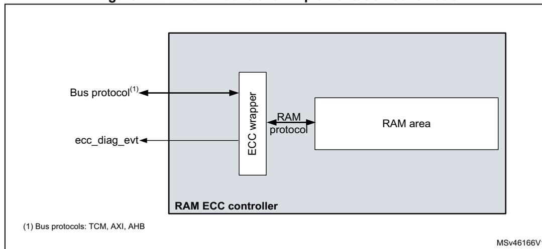
The diagram illustrates the internal structure of a RAM ECC controller. A large grey rectangle represents the 'RAM ECC controller'. Inside it, on the left, is a vertical white rectangle labeled 'ECC wrapper'. On the right is a white rectangle labeled 'RAM area'. A double-headed arrow labeled 'RAM protocol' connects the 'ECC wrapper' and the 'RAM area'. Outside the controller, on the left, a double-headed arrow labeled 'Bus protocol (1) ' points to the 'ECC wrapper'. Below it, a single-headed arrow labeled 'ecc_diag_evt' points away from the 'ECC wrapper'. A note at the bottom left states '(1) Bus protocols: TCM, AXI, AHB'. The identifier 'MSV46166V1' is in the bottom right corner.
A dedicated RAM ECC monitoring area is defined for each domain (see Section 3.3.2: RAMECC monitor mapping ). The RAMECC allows the collection of ECC diagnostic events from each RAM ECC controller and provides a mean for the CPU to verify the ECC status.
Figure 5 shows the connection schematic between the RAM ECC controller and the RAMECC monitoring unit.
Figure 5. Connection between RAM ECC controller and RAMECC monitoring unit
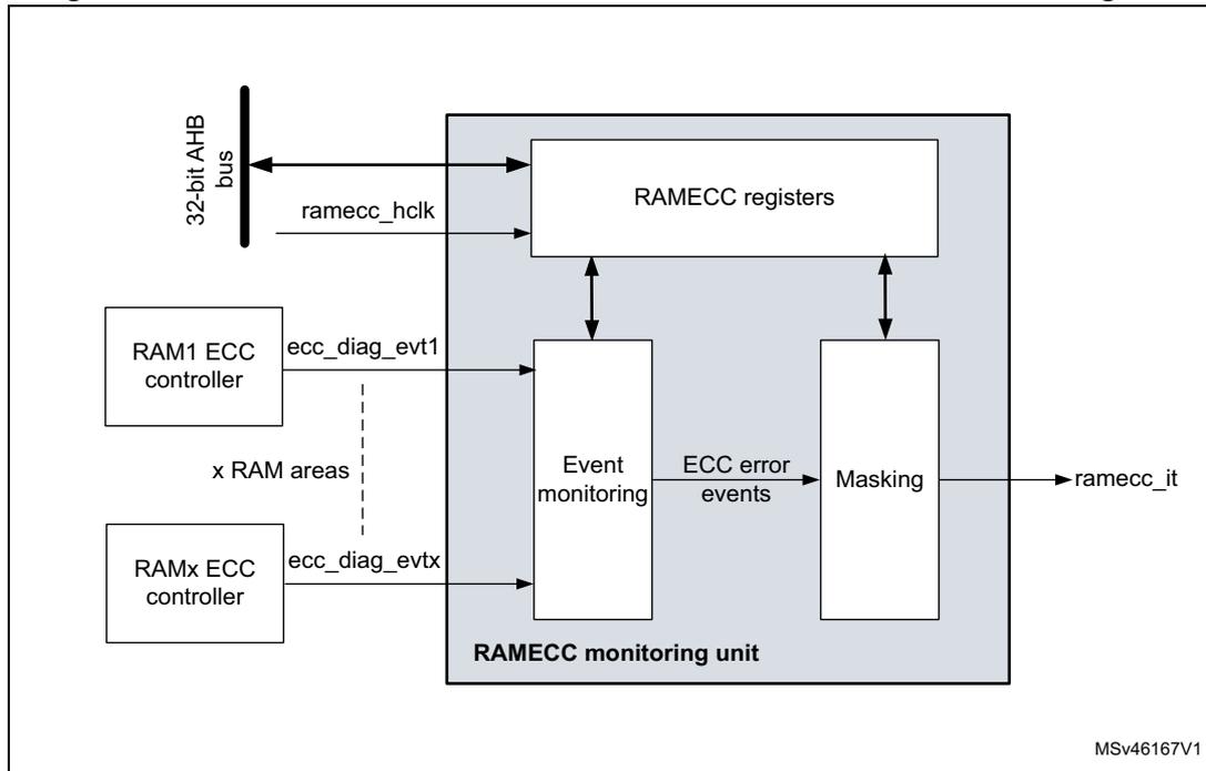
The diagram illustrates the internal architecture of the RAMECC monitoring unit and its connections. On the left, a vertical bar represents the '32-bit AHB bus'. An arrow labeled 'ramecc_hclk' points from this bus into the 'RAMECC monitoring unit' (a large grey box). Inside this unit, the 'RAMECC registers' block is at the top, connected to the bus. Below it are two blocks: 'Event monitoring' and 'Masking'. The 'RAMECC registers' block has bidirectional arrows connecting it to both the 'Event monitoring' and 'Masking' blocks. External 'RAM1 ECC controller' and 'RAMx ECC controller' blocks are shown on the left. The 'RAM1 ECC controller' sends an 'ecc_diag_evt1' signal to the 'Event monitoring' block. The 'RAMx ECC controller' sends an 'ecc_diag_evt x' signal to the same block. A dashed line labeled 'x RAM areas' is positioned between these two controllers. The 'Event monitoring' block sends 'ECC error events' to the 'Masking' block. Finally, an arrow labeled 'ramecc_it' exits the 'Masking' block to the right. The identifier 'MSV46167V1' is located in the bottom right corner of the diagram area.
3.3.1 RAMECC internal signals
Table 16 lists the internal signals that control the RAMECC unit.
Table 16. RAMECC internal input/output signals
| Internal signal name | Signal type | Description |
|---|---|---|
| ramecc_hclk | Input | AHB clock |
| ecc_diag_evt x | Input | ECC diagnostic event generated by RAMx ECC controller x |
| ramecc_it | Output | Interrupt generated by the RAMECC monitoring unit when an ECC error is detected. |
3.3.2 RAMECC monitor mapping
STM32H7Rx/7Sx devices features two RAMECC monitoring units The inputs from the ECC controllers are mapped as described in Table 17 . The RAM ECC event monitoring status and configuration registers are described in Section 3.6: RAMECC registers .
Table 17. ECC controller mapping
| RAMECC units (1) | Monitor number | SRAM ECC event monitoring status and configuration registers | Size in Kbytes | Address Offset | |
|---|---|---|---|---|---|
| ECC_DIAG_D1 (AXI SRAM) | 0 | AXI SRAM1 ECC monitoring unit | See Table 9: SRAM1 / ITCM configurations | 0x20 | |
| 1 | ITCM-RAM ECC monitoring unit | 0x40 | |||
| 2 | DTCM-RAM ECC monitoring unit | D0TCM | See Table 10: SRAM3 / DTCM configurations | 0x60 | |
| 3 | D1TCM | 0x80 | |||
| 4 | AXI SRAM3 ECC monitoring unit | 0xA0 | |||
| ECC_DIAG_D2 (Backup/Vbat domain) | 0 | Reserved | 0x20 | ||
| 1 | BKPRAM ECC monitoring unit | 4 | 0x40 | ||
1. See Table 7: Register boundary addresses .
Single and double ECC errors
When a single error is detected, it is automatically corrected and the SEDCF bits are set in the RAMECC monitor x status register (RAMECC_MxSR) . When a double error is detected, the DEDF bit are set in the RAMECC monitor x status register (RAMECC_MxSR) . An interrupt is generated if enabled by the GECCSEIE and GIE bits in the RAMECC interrupt enable register (RAMECC_IER) .
For single and double errors:
- • An interrupt is generated if enabled by the GECCSEIE and GIE bit in the RAMECC interrupt enable register (RAMECC_IER) . Single errors cannot be detected when the SEDC bit is set.
- • the context: failing address, data, ECC code are stored in the RAMECC monitor x failing address register (RAMECC_MxFAR) , RAMECC monitor x failing data low register (RAMECC_MxFDRL) , RAMECC monitor x failing data high register (RAMECC_MxFDRH) and RAMECC monitor x failing ECC error code register (RAMECC_MxFECR) if enabled by the ECCELEN bit in the RAMECC monitor x configuration register (RAMECC_MxCR) .
Caution: Double errors cannot be detected when the DEDF bit is set.
3.3.3 ECC fault injection test on SRAM1, SRAM3, and TCM
In order to test the ECC a mechanism, allow to test, 1 or 2 bits by word (for single or double error test respectively) and ECC alteration.
- • ECCTEA[1:0] = 00 or 11: Normal mode, ECC and DATA memory access granted
- • ECCTEA[1:0] = 01: ECC memory access mode granted, data memory access gated
- • ECCTEA[1:0] = 10: ECC memory access mode gated, data memory access granted
example:
initialization
- 1. Set the normal mode: ECCTEA[1:0] = 00
- 2. Write 0xCAFEDECA, ECC = 0x19 (computed by ECC module)
data modification
- 3. bloc ECC memory access: ECCTEA[1:0] = 10
- 4. Grant data modification: Write 0xCAFEDECB (last bit flipped)
- 5. return to normal mode: ECCTEA[1:0] = 00
- 6. READ 0xCAFEDECB with ECC = 19 single error = '1' (if enabled a flag is set and an interrupt to the NVIC is generated)
An ECC fault injection test triggers a system break events in TIM1/TIM15/TIM16/TIM17 if one of the following bits is set in the SBS_BKLOCKR register:
- • ARAM1ECC_BL
- • ARAM3ECC_BL
- • ITCMECC_BL
- • DTCMECC_BL
This implies that the test must be performed while the PWM outputs of the timers are in idle state.
3.4 RAMECC low-power modes
Table 18. Effect of low-power modes on RAMECC
| Mode | Description |
|---|---|
| Sleep | No effect. RAMECC interrupts cause the device to exit the Sleep mode. |
| Stop | The content of RAMECC registers is kept. The ECC is functional and ECC error interrupt causes the device to exit from Stop. |
| Standby | The RAMECC peripheral is powered down and must be reinitialized after exiting Standby. |
3.5 RAMECC interrupts
Table 19 lists the RAMECC interrupt requests.
Table 19. RAMECC interrupt requests
| Interrupt acronym | Interrupt event | Event flag | Enable control bit | Interrupt clear method | Exit the Sleep/Stop mode | Exit the Standby modes |
|---|---|---|---|---|---|---|
| RAMECC | ECC single error detection and correction | SEDCF | GECCSEIE ECCSEIE | Write 0 in SEDCF | Yes | No |
| ECC double error detection | DEDF | GECCDEIE GIE | Write 0 in DEDF | Yes | No |
3.6 RAMECC registers
RAMECC registers can be accessed only in 32-bit (word) mode. Byte and half-word formats are not allowed.
In the registers described below, x refers to:
- • SRAM1/2/3/4 when x = 1/2/3/4 respectively
- • BKPSRAM when x = 5
3.6.1 RAMECC interrupt enable register (RAMECC_IER)
Address offset: 0x00
Reset value: 0x0000 0000
| 31 | 30 | 29 | 28 | 27 | 26 | 25 | 24 | 23 | 22 | 21 | 20 | 19 | 18 | 17 | 16 |
|---|---|---|---|---|---|---|---|---|---|---|---|---|---|---|---|
| Res. | Res. | Res. | Res. | Res. | Res. | Res. | Res. | Res. | Res. | Res. | Res. | Res. | Res. | Res. | Res. |
| 15 | 14 | 13 | 12 | 11 | 10 | 9 | 8 | 7 | 6 | 5 | 4 | 3 | 2 | 1 | 0 |
| Res. | Res. | Res. | Res. | Res. | Res. | Res. | Res. | Res. | Res. | Res. | Res. | GECCDEBIE | GECCDEIE | GECCSEIE | GIE |
| rw | rw | rw | rw |
Bits 31:4 Reserved, must be kept at reset value.
Bit 3 GECCDEBIE : Global ECC double error on byte write (BW) interrupt enable
When GECCDEBIE bit is set to 1, an interrupt is generated when an ECC double detection error occurs during a byte write operation to RAM (incomplete word write).
0: no interrupt generated when an ECC double detection error occurs on byte write
1: interrupt generated if an ECC double detection error occurs on byte write
Bit 2 GECCDEIE : Global ECC double error interrupt enable
When GECCDEIE bit is set to 1, an interrupt is generated when an ECC double detection error occurs during a read operation from RAM.
0: no interrupt generated when an ECC double detection error occurs
1: interrupt generated if an ECC double detection error occurs
Bit 1 GECCSEIE : Global ECC single error interrupt enable
When GECCSEIE bit is set to 1, an interrupt is generated when an ECC single error occurs during a read operation from RAM.
0: no interrupt generated when an ECC single error occurs
1: interrupt generated when an ECC single error occurs
Bit 0 GIE : Global interrupt enable
When GIE bit is set to 1, an interrupt is generated when an enabled global ECC error (GECCDEBIE, GECCDEIE or GECCSEIE) occurs.
0: no interrupt generated when an ECC error occurs
1: interrupt generated when an ECC error occurs
3.6.2 RAMECC monitor x configuration register (RAMECC_MxCR)
Address offset: \( 0x00 + 0x20 * (x+1) \) , ( \( x = 0 \) to \( 4 \) )
Reset value: \( 0x0000\ 0000 \)
\( x \) is the ECC monitoring unit number
| 31 | 30 | 29 | 28 | 27 | 26 | 25 | 24 | 23 | 22 | 21 | 20 | 19 | 18 | 17 | 16 |
|---|---|---|---|---|---|---|---|---|---|---|---|---|---|---|---|
| Res. | Res. | Res. | Res. | Res. | Res. | Res. | Res. | Res. | Res. | Res. | Res. | Res. | Res. | ECCTEA[1:0] | |
| rw | rw | ||||||||||||||
| 15 | 14 | 13 | 12 | 11 | 10 | 9 | 8 | 7 | 6 | 5 | 4 | 3 | 2 | 1 | 0 |
| Res. | Res. | Res. | Res. | Res. | Res. | Res. | ECCDEBWCEN | ECCDECEN | ECCSE CEN | ECCEL EN | ECCDE BWIE | ECCDE IE | ECCSE IE | Res. | Res. |
| rw | rw | rw | rw | rw | rw | rw |
Bits 31:18 Reserved, must be kept at reset value.
Bits 17:16 ECCTEA[1:0] : ECC Test ECC access
00: inactive
01: write and read access blocked on data memory
10: write and read access blocked on ECC memory
11: inactive
Bits 15:9 Reserved, must be kept at reset value.
Bit 8 ECCDEBWCEN : ECC double error on byte write (BW) counter enable
When ECCDEBWCEN bit is set to 1, the occurrence counter is incremented when an ECC double detection error occurs during a byte write operation to RAM.
0: no counter increment when an ECC double detection error occurs on byte write
1: counter increment when an ECC double detection error occurs on byte write
Bit 7 ECCDECEN : ECC double error counter enable
When ECCDECEN bit is set to 1, the occurrence counter is incremented when an ECC double detection error occurs during a read operation from RAM.
0: no counter increment when an ECC double detection error occurs
1: counter increment when an ECC double detection error occurs
Bit 6 ECCSECEN : ECC single error counter enable
When ECCSECEN bit is set to 1, the occurrence counter is incremented when an ECC single error occurs during a read operation from RAM.
0: no counter increment when an ECC single error occurs
1: counter increment when an ECC single error occurs
Bit 5 ECCELEN : ECC error latching enable
When ECCELEN bit is set to 1, if an ECC error occurs (both for single error correction or double detection) during a read operation, the context (address, data and ECC code) that generated the error are latched to their respective registers.
0: no error context preserved when an ECC error occurs
1: error context preserved when an ECC error occurs
Bit 4 ECCDEBWIE : ECC double error on byte write (BW) interrupt enable
When ECCDEBWIE bit is set to 1, monitor x generates an interrupt when an ECC double detection error occurs during a byte write operation to RAM.
0: no interrupt generated when an ECC double detection error occurs on byte write
1: interrupt generated if an ECC double detection error occurs on byte write
Bit 3 ECCDEIE : ECC double error interrupt enable
When ECCDEIE bit is set to 1, monitor x generates an interrupt when an ECC double detection error occurs during a read operation from RAM.
0: no interrupt generated when an ECC double detection error occurs
1: interrupt generated if an ECC double detection error occurs
Bit 2 ECCSEIE : ECC single error interrupt enable
When ECCSEIE bit is set to 1, monitor x generates an interrupt when an ECC single error occurs during a read operation from RAM.
0: no interrupt generated when an ECC single error occurs
1: interrupt generated when an ECC single error occurs
Bits 1:0 Reserved, must be kept at reset value.
3.6.3 RAMECC monitor x status register (RAMECC_MxSR)
Address offset: \( 0x24 + 0x20 * x \) , ( \( x = 0 \) to \( 4 \) )
Reset value: 0x0000 0000
| 31 | 30 | 29 | 28 | 27 | 26 | 25 | 24 | 23 | 22 | 21 | 20 | 19 | 18 | 17 | 16 |
|---|---|---|---|---|---|---|---|---|---|---|---|---|---|---|---|
| Res. | Res. | Res. | Res. | Res. | Res. | Res. | Res. | Res. | Res. | Res. | Res. | Res. | Res. | Res. | Res. |
| 15 | 14 | 13 | 12 | 11 | 10 | 9 | 8 | 7 | 6 | 5 | 4 | 3 | 2 | 1 | 0 |
| Res. | Res. | Res. | Res. | Res. | Res. | Res. | Res. | Res. | Res. | Res. | Res. | Res. | DEBW DF | DEDF | SEDCF |
| rc_w0 | rc_w0 | rc_w0 |
Bits 31:3 Reserved, must be kept at reset value.
Bit 2 DEBWDF : ECC double error on byte write (BW) detected flag
This bit is set by hardware. It is cleared by software by writing a 0
0: no error detected
1: error detected
Bit 1 DEDF : ECC double error detected flag
This bit is set by hardware. It is cleared by software by writing a 0
0: no error detected
1: error detected
Bit 0 SEDCF : ECC single error detected and corrected flag
This bit is set by hardware. It is cleared by software by writing a 0
0: no error detected and corrected
1: error detected and corrected
3.6.4 RAMECC monitor x failing address register (RAMECC_MxFAR)
Address offset: \( 0x28 + 0x20 * x \) , ( \( x = 0 \) to \( 4 \) )
Reset value: 0x0000 0000
| 31 | 30 | 29 | 28 | 27 | 26 | 25 | 24 | 23 | 22 | 21 | 20 | 19 | 18 | 17 | 16 |
|---|---|---|---|---|---|---|---|---|---|---|---|---|---|---|---|
| FADD[31:16] | |||||||||||||||
| r | r | r | r | r | r | r | r | r | r | r | r | r | r | r | r |
| 15 | 14 | 13 | 12 | 11 | 10 | 9 | 8 | 7 | 6 | 5 | 4 | 3 | 2 | 1 | 0 |
| FADD[15:0] | |||||||||||||||
| r | r | r | r | r | r | r | r | r | r | r | r | r | r | r | r |
Bits 31:0 FADD[31:0] : ECC error failing address
When an ECC error occurs the FADD bitfield contains the address that generated the ECC error.
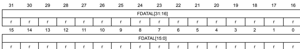
3.6.5 RAMECC monitor x failing data low register (RAMECC_MxFDRL)
Address offset: \( 0x2C + 0x20 * x \) , ( \( x = 0 \) to \( 4 \) )
Reset value: 0x0000 0000
| 31 | 30 | 29 | 28 | 27 | 26 | 25 | 24 | 23 | 22 | 21 | 20 | 19 | 18 | 17 | 16 |
| FDATAL[31:16] | |||||||||||||||
| r | r | r | r | r | r | r | r | r | r | r | r | r | r | r | r |
| 15 | 14 | 13 | 12 | 11 | 10 | 9 | 8 | 7 | 6 | 5 | 4 | 3 | 2 | 1 | 0 |
| FDATAL[15:0] | |||||||||||||||
| r | r | r | r | r | r | r | r | r | r | r | r | r | r | r | r |
Bits 31:0 FDATAL[31:0] : Failing data low
When an ECC error occurs the FDATAL bitfield contains the LSB part of the data that generated the error. For 32-bit word SRAM, this bitfield contains the full memory word that generated the error.
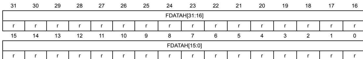
3.6.6 RAMECC monitor x failing data high register (RAMECC_MxFDRH)
Address offset: \( 0x30 + 0x20 * x \) , ( \( x = 0 \) to \( 4 \) )
Reset value: 0x0000 0000
| 31 | 30 | 29 | 28 | 27 | 26 | 25 | 24 | 23 | 22 | 21 | 20 | 19 | 18 | 17 | 16 |
| FDATAH[31:16] | |||||||||||||||
| r | r | r | r | r | r | r | r | r | r | r | r | r | r | r | r |
| 15 | 14 | 13 | 12 | 11 | 10 | 9 | 8 | 7 | 6 | 5 | 4 | 3 | 2 | 1 | 0 |
| FDATAH[15:0] | |||||||||||||||
| r | r | r | r | r | r | r | r | r | r | r | r | r | r | r | r |
Bits 31:0 FDATAH[31:0] : Failing data high (64-bit memory)
When an ECC error occurs the FDATAH bitfield contains the MSB part of the data that generated the error.
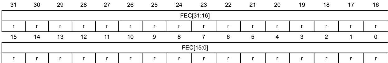
3.6.7 RAMECC monitor x failing ECC error code register (RAMECC_MxFECR)
Address offset: 0x34 + 0x20 * x, (x = 0 to 4)
Reset value: 0x0000 0000
| 31 | 30 | 29 | 28 | 27 | 26 | 25 | 24 | 23 | 22 | 21 | 20 | 19 | 18 | 17 | 16 |
| FEC[31:16] | |||||||||||||||
| r | r | r | r | r | r | r | r | r | r | r | r | r | r | r | r |
| 15 | 14 | 13 | 12 | 11 | 10 | 9 | 8 | 7 | 6 | 5 | 4 | 3 | 2 | 1 | 0 |
| FEC[15:0] | |||||||||||||||
| r | r | r | r | r | r | r | r | r | r | r | r | r | r | r | r |
Bits 31:0 FEC[31:0] : Failing error code
When an ECC error occurs the FEC bitfield contains the ECC failing code that generated the error.
3.6.8 RAMECC register map
Table 20. RAMECC register map and reset values
| Offset | Register name reset value | 31 | 30 | 29 | 28 | 27 | 26 | 25 | 24 | 23 | 22 | 21 | 20 | 19 | 18 | 17 | 16 | 15 | 14 | 13 | 12 | 11 | 10 | 9 | 8 | 7 | 6 | 5 | 4 | 3 | 2 | 1 | 0 |
|---|---|---|---|---|---|---|---|---|---|---|---|---|---|---|---|---|---|---|---|---|---|---|---|---|---|---|---|---|---|---|---|---|---|
| 0x00 | RAMECC_IER | Res. | Res. | Res. | Res. | Res. | Res. | Res. | Res. | Res. | Res. | Res. | Res. | Res. | Res. | Res. | Res. | Res. | Res. | Res. | Res. | Res. | Res. | Res. | Res. | Res. | Res. | Res. | Res. | GECCDEBIE | GECCDEIE | GECCSEIE | GIE |
| Reset value | - | - | - | - | - | - | - | - | - | - | - | - | - | - | - | - | - | - | - | - | - | - | - | - | - | - | - | - | 0 | 0 | 0 | 0 | |
| 0x20 * x | RAMECC_MxCR | Res. | Res. | Res. | Res. | Res. | Res. | Res. | Res. | Res. | Res. | Res. | Res. | Res. | Res. | ECCTEA[1:0] | Res. | Res. | Res. | Res. | Res. | Res. | Res. | ECCDEBWCEN | ECCDECEN | ECCSECEN | ECCELEN | ECCDEBIE | ECCDEIE | ECCSEIE | Res. | Res. | |
| Reset value | - | - | - | - | - | - | - | - | - | - | - | - | - | - | 0 | 0 | - | - | - | - | - | - | - | 0 | 0 | 0 | 0 | 0 | 0 | 0 | - | - | |
| 0x24 + 0x20 * (x - 1) | RAMECC_MxSR | Res. | Res. | Res. | Res. | Res. | Res. | Res. | Res. | Res. | Res. | Res. | Res. | Res. | Res. | Res. | Res. | Res. | Res. | Res. | Res. | Res. | Res. | Res. | Res. | Res. | Res. | Res. | Res. | Res. | DEBWDF | DEDF | SEDCF |
| Reset value | - | - | - | - | - | - | - | - | - | - | - | - | - | - | - | - | - | - | - | - | - | - | - | - | - | - | - | - | - | 0 | 0 | 0 | |
| 0x28 + 0x20 * (x-1) | RAMECC_MxFAR | FADD[31:0] | |||||||||||||||||||||||||||||||
| Reset value | 0 | 0 | 0 | 0 | 0 | 0 | 0 | 0 | 0 | 0 | 0 | 0 | 0 | 0 | 0 | 0 | 0 | 0 | 0 | 0 | 0 | 0 | 0 | 0 | 0 | 0 | 0 | 0 | 0 | 0 | 0 | 0 | |
| 0x2C + 0x20 * (x-1) | RAMECC_MxFDRL | FDATAL[31:0] | |||||||||||||||||||||||||||||||
| Reset value | 0 | 0 | 0 | 0 | 0 | 0 | 0 | 0 | 0 | 0 | 0 | 0 | 0 | 0 | 0 | 0 | 0 | 0 | 0 | 0 | 0 | 0 | 0 | 0 | 0 | 0 | 0 | 0 | 0 | 0 | 0 | 0 | |
| 0x30 + 0x20 * (x-1) | RAMECC_MxFDRH | FDATAH[31:0] | |||||||||||||||||||||||||||||||
| Reset value | 0 | 0 | 0 | 0 | 0 | 0 | 0 | 0 | 0 | 0 | 0 | 0 | 0 | 0 | 0 | 0 | 0 | 0 | 0 | 0 | 0 | 0 | 0 | 0 | 0 | 0 | 0 | 0 | 0 | 0 | 0 | 0 | |
| 0x34 + 0x20 * (x-1) | RAMECC_MxFECR | FEC[31:0] | |||||||||||||||||||||||||||||||
| Reset value | 0 | 0 | 0 | 0 | 0 | 0 | 0 | 0 | 0 | 0 | 0 | 0 | 0 | 0 | 0 | 0 | 0 | 0 | 0 | 0 | 0 | 0 | 0 | 0 | 0 | 0 | 0 | 0 | 0 | 0 | 0 | 0 | |