2. Memory and bus architecture
2.1 System architecture
The STM32H7Rx/7Sx architecture relies on a Arm Cortex-M7 core optimized for execution by means of Cache, TCM, AXI, and an AHB bus matrix. This architecture also features a 64-bit AXI, an 32-bit multilayer AHB bus matrix, and bus bridges allow interconnection of bus masters with bus slaves, as shown in Table 2: Bus-master-to-bus-slave interconnect .
Table 2. Bus-master-to-bus-slave interconnect
| Bus slave / type (1) | Bus master / type (1) | |||||||||||||||||
|---|---|---|---|---|---|---|---|---|---|---|---|---|---|---|---|---|---|---|
| Cortex-M7 - AXIM | Cortex-M7 - AHP | Cortex-M7 - ITCM | Cortex-M7 - DTCM | SDMMC1 | HPDMA - AXI | HPDMA - AHB | GPDMA - AHB | ICACHE_AHB | GPU2D_AXI1 | GPU2D_AXI2 | DCMIPP | GFXMMU | DMA2D | LTDC | ETH1 - AHB | SDMMC2 - AHB | OTG_HS - AHB | |
| Interconnect path and type (2) | ||||||||||||||||||
| ITCM | - | - | X | - | - | - | X | - | - | - | - | - | - | - | - | - | - | - |
| DTCM | - | - | - | X | - | - | X | - | - | - | - | - | - | - | - | - | - | - |
| FLASH | X | - | - | - | X | X (3) | - | X | - | - | - | - | - | X | - | X | - | X |
| AXI SRAM1 | X | - | - | - | X | X (3) | - | X | X | X | X | X | X | X | X | X | X | X |
| AXI SRAM2 | X | - | - | - | X | X (3) | - | X | X | X | X | X | X | X | X | X | X | X |
| AXI SRAM3 | X | - | - | - | X | X (3) | - | X | X | X | X | X | X | X | X | X | X | X |
| AXI SRAM4 | X | - | - | - | X | X (3) | - | X | X | X | X | X | X | X | X | X | X | X |
| AHB SRAM1/2 | X | X | - | - | - | X (3) | - | X | - | - | - | - | - | - | - | X | X | X |
| XSPI1 | X | - | - | - | X | X (3) | - | X | X | X | X | X | X | X | X | X | X | X |
| XSPI2 | X | - | - | - | X | X (3) | - | X | X | X | X | X | X | X | X | X | X | X |
| FMC | X | - | - | - | X | X (3) | - | X | X | X | X | X | X | X | X | X | X | X |
| GFXMMU | X | - | - | - | - | X | - | - | - | X | - | - | - | X | X | - | - | - |
| AHB1 peripherals | - | X | - | - | - | - | X (4) | X | - | - | - | - | - | - | - | - | - | - |
| APB1 peripherals | - | X | - | - | - | - | X (4) | X (5) | - | - | - | - | - | - | - | - | - | - |
| AHB2 peripherals | - | X | - | - | - | - | X | X | - | - | - | - | - | - | - | - | - | - |
| APB2 peripherals | - | X | - | - | - | - | X (4) | X (5) | - | - | - | - | - | - | - | - | - | - |
| AHB3 peripherals | - | X | - | - | - | - | - | X | - | - | - | - | - | - | - | - | - | - |
| AHB4 peripherals | - | X | - | - | - | - | X | X (5) | - | - | - | - | - | - | - | - | - | - |
| APB4 peripherals | - | X | - | - | - | - | X (4) | X (5) | - | - | - | - | - | - | - | - | - | - |
| AHB5 peripherals | - | X | - | - | - | - | X (4) | - | - | - | - | - | - | - | - | - | - | - |
| APB5 peripherals | - | X | - | - | - | - | - | - | - | - | - | - | - | - | - | - | - | - |
| Backup RAM | X | X | - | - | - | X (3) | - | X | - | - | - | - | - | - | - | - | X | - |
1. Bold font type denotes 64-bit bus, plain type denotes 32-bit bus.
2. "X" = access possible, "-" = access not possible.
3. Every transfer can be done in 64 bits
4. Refer to Table 102: Programmed HPDMA1 request for the AHB/APB peripheral request.
5. Refer to Table 94: Programmed GPDMA1 trigger
The bus matrix provides access from a master to a slave, enabling concurrent access and efficient operation even when several high-speed peripherals work simultaneously. This architecture is shown in the figure below.
Figure 1. System architecture
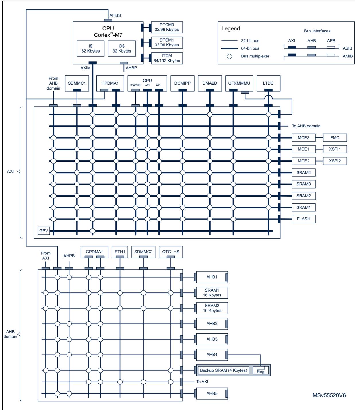
The diagram illustrates the system architecture of the MSv55520V6 microcontroller. At the top, a CPU Cortex®-M7 is shown with its internal components: IS 32 Kbytes , DS 32 Kbytes , DTCM0 32/96 Kbytes , DTCM1 32/96 Kbytes , and ITCM 64/192 Kbytes . The CPU is connected to an AHBS (32-bit bus) and an AXIM (64-bit bus) interface.
The AXI domain (top section) includes a bus matrix with multiple slave interfaces: SDMMC1 , HPDMA1 , ICACHE , GPU (connected to AXI and AHB ), DCMIPP , DMA2D , GFXMMU , and LTDC . It also features connections From AHB domain and To AHB domain . External slave interfaces on the right include MCE3 (FMC), MCE1 (XSPI1), MCE2 (XSPI2), SRAM4 , SRAM3 , SRAM2 , SRAM1 , and FLASH . A GPV (Graphics Processing Unit) is also connected to the AXI domain.
The AHB domain (bottom section) includes a bus matrix with slave interfaces: GPDMA1 , ETH1 , SDMMC2 , and OTG_HS . It features connections From AXI and To AXI . External slave interfaces on the right include AHB1 , SRAM1 16 Kbytes , SRAM2 16 Kbytes , AHB2 , AHB3 , AHB4 , Backup SRAM (4 Kbytes) (connected to Reg ), and AHB5 .
A Legend box in the top right defines the bus types and interfaces:
- 32-bit bus : Represented by a thin line.
- 64-bit bus : Represented by a thick line.
- Bus multiplexer : Represented by a circle.
- Bus interfaces : Shows icons for AXI , AHB , and APB interfaces, labeled as ASIB and AMIIB .
The identifier MSv55520V6 is located in the bottom right corner of the diagram.
2.1.1 Bus matrices
AXI bus matrix
The multi AXI bus matrix ensures and arbitrates concurrent accesses from multiple masters to multiple slaves. This allows efficient simultaneous operation of high-speed peripherals.
The arbitration uses a round-robin algorithm with QoS capability.
Refer to Section 2.2: AXI interconnect matrix (AXIM) for more information on AXI interconnect.
AHB bus matrices
The AHB bus matrices ensure and arbitrate concurrent accesses from multiple masters to multiple slaves. This allows efficient simultaneous operation of high-speed peripherals.
The arbitration uses a round-robin algorithm.
2.1.2 Bus-to-bus bridges
To allow peripherals with different types of buses to communicate together, there is a number of bus-to-bus bridges in the system.
The AHB/APB bridges allow connecting peripherals on APB1, APB2, APB4, APB5 to AHB1, AHB2, AHB4 and AHB5, respectively. These AHB/APB bridges provide full synchronous interfacing, which allows the APB peripherals to operate with clocks independent of AHB that they connect to.
The AHB/APB bridges also allow APB1, APB2 and APB4 peripherals to connect to GPDMA1 peripheral buses, without transiting through the AHB BUS.
The AHB/APB bridges convert 8-bit / 16-bit APB data to 32-bit AHB data, by replicating it to the three upper bytes / the upper half-word of the 32-bit word.
The AXI bus matrix incorporates AHB/AXI bus bridge functionality on its slave bus interfaces. The AXI/AHB bus bridges on its master interfaces marked as 32-bit in Figure 1: System architecture are outside the matrix.
The Cortex-M7 CPU provides AHB/TCM-bus (ITCM and DTCM buses) translation from its AHBS slave AHB, allowing the HPDMA controller to access the ITCM and DTCM.
Note: When a 8- or 16-bit access is performed on an APB register, the access is transformed into a 32-bit access: the bridge duplicates the 8- or 16-bit data to feed the 32-bit vector.
2.1.3 TCM-buses
The DTCM and ITCM (data and instruction tightly coupled RAMs) are connected through dedicated TCM buses directly to the Cortex-M7 core. The HPDMA controller can access the DTCM and ITCM through AHBS, a specific CPU slave AHB. The DTCM and ITCM are accessed by Cortex-M7 at CPU clock speed, with zero wait states.
2.1.4 CPU buses
Cortex-M7 AXIM bus
The Cortex-M7 CPU uses the 64-bit AXIM bus to access all memories (excluding ITCM, and DTCM)
The AXIM bus connects the CPU to the AXI bus matrix in the core domain.
Cortex-M7 ITCM bus
The Cortex-M7 CPU uses the 64-bit ITCM bus for fetching instructions from and accessing data in the ITCM.
Cortex-M7 DTCM bus
The Cortex-M7 CPU uses the 2x32-bit DTCM bus for accessing data in the DTCM. The 2x32-bit DTCM bus allows load/load and load/store instruction pairs to be dual-issued on the DTCM memory. It can also fetch instructions.
Cortex-M7 AHBS bus
The Cortex-M7 CPU uses the 32-bit AHBS slave bus to allow the HPDMA controller to access the ITCM and the DTCM.
Cortex-M7 AHBP bus
The Cortex-M7 CPU uses the 32-bit AHBP bus for accessing AHB1, AHB2, AHB3, AHB4, APB1, APB2 and APB4 peripherals via the AHB bus matrix.
2.1.5 Bus master peripherals
SDMMC1-bus
The SDMMC1 uses a 32-bit bus, connected to the AXI bus matrix, through which it can access internal AXI SRAM and Flash memories, and external memories through the XSPIs controller and the FMC.
SDMMC2-bus
The SDMMC2 uses a 32-bit bus, connected to the AHB bus matrix. Through the system bus matrices, it can access the internal AXI SRAM, SRAM1, SRAM2, SRAM3 SRAM4, backup RAM, Flash memory, and external memories through the XSPIs controller and the FMC.
HPDMA-bus
The HPDMA controller has two bus masters: an AXI 64-bit bus, connected to the AXI bus matrix and an AHB 32-bit bus connected to the Cortex-M7 AHBS slave bus.
The HPDMA is optimized for DMA data transfers between memories since it supports linked list transfers that allow performing a chained list of transfers without the need for CPU intervention. Through the system bus matrices and the Cortex-M7 AHBS slave bus, the HPDMA can access all internal and external memories through the CTOSPIs controller and the FMC.
GPDMA-bus
The GPDMA controller has two 32-bit AHB bus masters connected to the AHB bus matrix.
The memory bus allows the GPDMA data transfers between memories. Through the system bus matrices, the memory bus can access all internal memories except ITCM and DTCM, and external memories through the XSPIs controller and the FMC. It also supports linked list transfers
The peripheral bus allows the GPDMA data transfers between two peripherals, between two memories or between a peripheral and a memory. Through the system bus matrices, the peripheral bus can access all internal memories except ITCM and DTCM, external memories through the XSPIs controller and the FMC, and all AHB and APB peripherals. A direct access to APB1 and APB2 is available, without passing through AHB1.
DMA2D-bus (Chrom-Art Accelerator)
The DMA2D graphics accelerator uses a 64-bit bus, connected to the AXI bus matrix. Through the system bus matrices, internal AXI SRAM, SRAM1, SRAM2, SRAM3, SRAM4 Flash memories and external memories through the XSPIs controller and the FMC.
LTDC-bus (LCD-TFT controller)
The LCD-TFT display controller, LTDC, uses a 64-bit bus, connected to the AXI bus matrix, through which it can access internal AXI SRAM and external memories through the XSPIs controller and the FMC.
Ethernet MAC-bus
The Ethernet MAC uses a 32-bit bus, connected to the AHB bus matrix. Through the system bus matrices, it can access all internal memories except backup RAM, ITCM, DTCM it can also access external memories, through the XSPIs controller and the FMC.
USB OTG-bus
The USBHS1 peripheral uses 32-bit buses, connected to the AHB bus matrix. Through the system bus matrices, it can access all internal memories except backup RAM, ITCM, DTCM and it access the external memories, through the XSPIs controller and the FMC.
2.1.6 GPU2D-bus
These buses connect the GPU2D master interfaces to the bus matrix. These buses are used to load/store data from/to the memory. These buses target the GFXMMU in addition to the data memories: internal Flash memory, internal SRAMs (SRAM1, SRAM2, SRAM3 and SRAM4) and external memories through FMC, XSPIs. A 16-Kbyte data cache (ICACHE) is present on the GPU2D M0 bus in order to improve performances.
2.1.7 GFXMMU-bus
This bus connects the GFXMMU master interface to the bus matrix. This bus is used only by the GFXMMU to load/store data from/to the memory. This bus targets the data memories: internal Flash memory, internal SRAMs (SRAM1, SRAM2, SRAM3 and SRAM4) and external memories through FMC, XSPIs. The GFXMMU has also a slave bus connection to be accessed by graphical peripheral master buses.
2.1.8 Clocks to functional blocks
Upon reset, clocks to blocks such as peripherals and some memories are disabled (except for the SRAM, DTCM, ITCM and Flash memory). To operate a block with no clock upon reset, the software must first enable its clock through RCC_AHBxENR or RCC_APBxENR register, respectively.
2.2 AXI interconnect matrix (AXIM)
2.2.1 AXI introduction
The AXI (advanced extensible interface) interconnect is based on the Arm® CoreLink™ NIC-400 Network Interconnect. The interconnect has eleven initiator ports, or ASIBs (AMBA slave interface blocks), and ten target ports, or AMIBs (AMBA master interface blocks). The ASIBs are connected to the AMIBs via an AXI switch matrix.
Each ASIB is a slave on an AXI bus or AHB (advanced high-performance bus). Similarly, each AMIB is a master on an AXI or AHB bus. Where an ASIB or AMIB is connected to an AHB, it converts between the AHB and the AXI protocol.
The AXI interconnect includes a GPV (global programmer view) which contains registers for configuring certain parameters, such as the QoS (quality of service) level at each ASIB.
Any accesses to unallocated address space are handled by the default slave, which generates the return signals. This ensures that such transactions complete and do not block the issuing master and ASIB.
2.2.2 AXI interconnect main features
- • 64-bit AXI bus switch matrix with eleven ASIBs and ten AMIBs
- • AHB/AXI bridge function built into the ASIBs
- • concurrent connectivity of multiple ASIBs to multiple AMIBs
- • programmable traffic priority management (QoS - quality of service)
- • software-configurable via GPV
2.2.3 AXI interconnect functional description
Block diagram
The AXI interconnect is shown in Figure 2 .
Figure 2. AXI interconnect
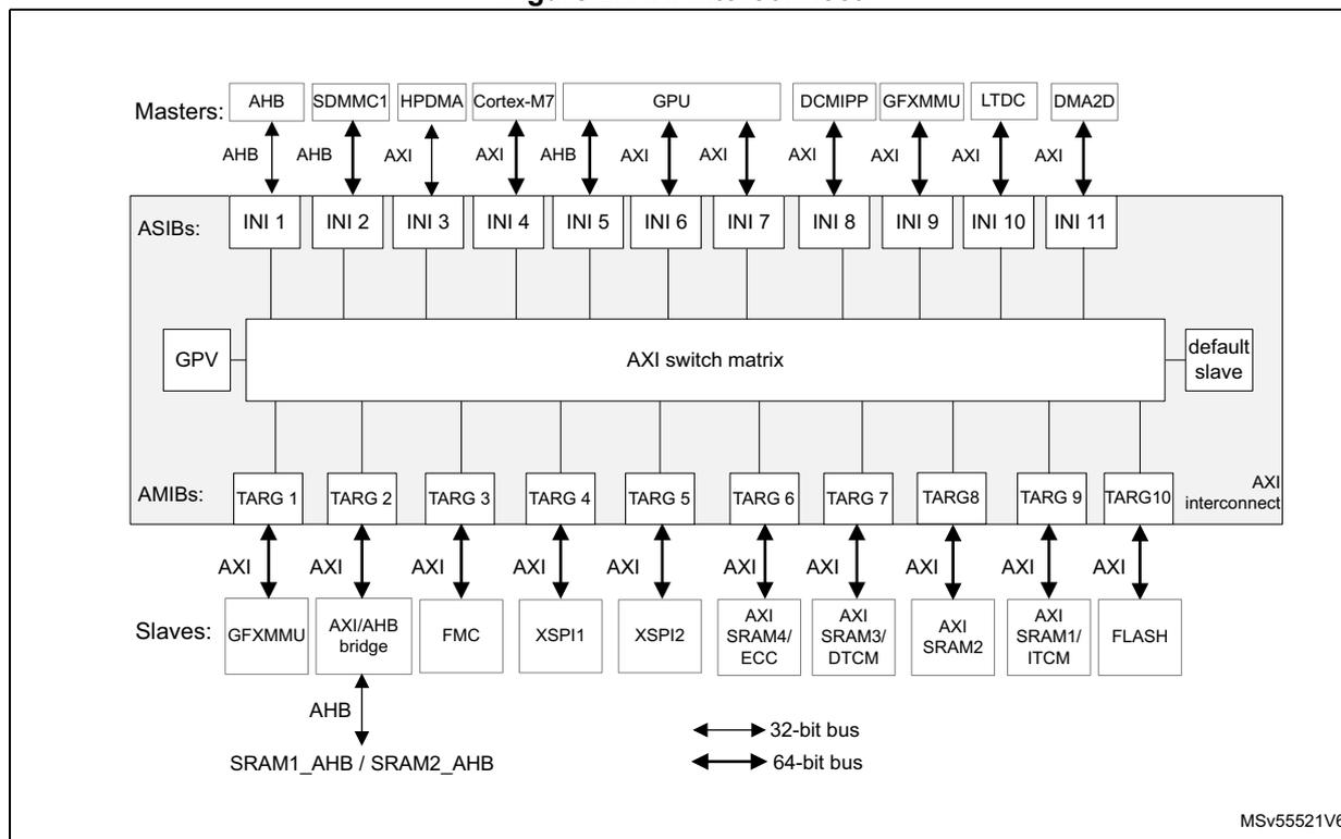
The diagram illustrates the AXI interconnect architecture. At the top, a row of Masters is shown: AHB, SDMMC1, HPDMA, Cortex-M7, GPU, DCMIPP, GFXMMU, LTDC, and DMA2D. These masters are connected to a row of ASIBs (INI 1 through INI 11) via various bus types: AHB (for AHB, SDMMC1, Cortex-M7), AXI (for HPDMA, GPU, DCMIPP, GFXMMU, LTDC, DMA2D), and AHB (for Cortex-M7). The ASIBs are connected to a central AXI switch matrix . The matrix also includes a GPV (Graphics Processing Unit) on the left and a default slave on the right. Below the matrix is a row of AMIBs (TARG 1 through TARG 10), which are connected to the matrix and to a row of Slaves . The slaves include GFXMMU, AXI/AHB bridge, FMC, XSPI1, XSPI2, AXI SRAM4/ECC, AXI SRAM3/DTCM, AXI SRAM2, AXI SRAM1/ITCM, and FLASH. The AXI interconnect is labeled on the right side of the diagram. At the bottom, a legend indicates that a single-headed arrow represents a 32-bit bus and a double-headed arrow represents a 64-bit bus. The SRAM1_AHB / SRAM2_AHB block is connected to the AXI/AHB bridge via an AHB bus. The reference number MSv55521V6 is located in the bottom right corner.
ASIB configuration
Table 3 summarizes the characteristics of the ASIBs.
Table 3. ASIB configuration
| ASIB | Connected master | Protocol | Bus width | R/W issuing |
|---|---|---|---|---|
| INI 1 | AHB from AHB peripherals | AHB-lite | 32 | 1/1 |
| INI 2 | SDMMC1 | AHB-lite | 32 | 1/1 |
| INI 3 | HPDMA | AXI4 | 64 | 8/8 |
| INI 4 | Cortex-M7 | AXI4 | 64 | 7/32 |
| INI 5 | GPU | AHB | 64 | 1/1 |
| INI 6 | AXI4 | 64 | 1/2 | |
| INI 7 | AXI4 | 64 | 1/0 | |
| INI 8 | DCMIPP | AXI4 | 64 | 0/1 |
| INI 9 | GFXMMU | AXI4 | 64 | 1/2 |
| INI 10 | LTDC | AXI4 | 64 | 2/0 |
| INI 11 | DMA2D | AXI4 | 64 | 2/1 |
AMIB configuration
Table 4 summarizes the characteristics of the AMIBs.
Table 4. AMIB configuration
| AMIB | Connected slave | Protocol | Bus width | R/W/Total acceptance |
|---|---|---|---|---|
| TARG 1 | GFXMMU | AXI4 | 64 | 2/2/4 |
| TARG 2 | AHB Sram | AXI4 (1) | 32 | 1/1/2 |
| TARG 3 | FMC | AXI4 | 64 | 1/1/2 |
| TARG 4 | XSPI1 | AXI4 | 64 | 1/1/2 |
| TARG 5 | XSPI2 | AXI4 | 64 | 1/1/2 |
| TARG 6 | AXI SRAM (2) | AXI4 | 64 | 2/2/4 |
| TARG 7 | AXI SRAM (3) | AXI4 | 64 | 2/2/4 |
| TARG 8 | AXI SRAM | AXI4 | 64 | 2/2/4 |
| TARG 9 | AXI SRAM (4) | AXI4 | 64 | 2/2/4 |
| TARG 10 | FLASH | AXI4 | 64 | 2/2/4 |
- 1. Conversion to AHB protocol is done via an AXI/AHB bridge sitting between AXI interconnect and the connected slave.
- 2. SRAM shared with the ECC ( Table 11: SRAM4 / ECC configurations )
- 3. SRAM shared with the DTCM ( SRAM3 / DTCM configurations )
- 4. SRAM shared with the ITCM ( SRAM1 / ITCM configurations )
Quality of service (QoS)
The AXI switch matrix uses a priority-based arbitration when two ASIB simultaneously attempt to access the same AMIB. Each ASIB has programmable read channel and write channel priorities, known as QoS, from 0 to 15, such that the higher the value, the higher the priority. The read channel QoS value is programmed in the AXI interconnect - INI x read QoS register (AXI_INIx_READ_QOS) , and the write channel in the AXI interconnect - INI x write QoS register (AXI_INIx_WRITE_QOS) . The default QoS value for all channels is 0 (lowest priority).
If two coincident transactions arrive at the same AMIB, the higher priority transaction passes before the lower priority. If the two transactions have the same QoS value, then a least-recently-used (LRU) priority scheme is adopted.
The QoS values should be programmed according to the latency requirements for the application. Setting a higher priority for an ASIB ensures a lower latency for transactions initiated by the associated bus master. This can be useful for real-time-constrained tasks, such as graphics processing (LTDC, DMA2D). Assigning a high priority to masters that can make many and frequent accesses to the same slave (such as the Cortex-M7 CPU) can block access to that slave by other lower-priority masters.
Global programmer view (GPV)
The GPV contains configuration registers for the AXI interconnect. These registers are only accessible by the Cortex-M7 CPU.
2.2.4 AXI interconnect registers
AXI interconnect - peripheral ID4 register (AXI_PERIPH_ID_4)
Address offset: 0x1FD0
Reset value: 0x0000 0004
| 31 | 30 | 29 | 28 | 27 | 26 | 25 | 24 | 23 | 22 | 21 | 20 | 19 | 18 | 17 | 16 |
|---|---|---|---|---|---|---|---|---|---|---|---|---|---|---|---|
| Res. | Res. | Res. | Res. | Res. | Res. | Res. | Res. | Res. | Res. | Res. | Res. | Res. | Res. | Res. | Res. |
| 15 | 14 | 13 | 12 | 11 | 10 | 9 | 8 | 7 | 6 | 5 | 4 | 3 | 2 | 1 | 0 |
| Res. | Res. | Res. | Res. | Res. | Res. | Res. | Res. | COUNT4K[3:0] | JEP106CON[3:0] | ||||||
| r | r | r | r | r | r | r | r | ||||||||
Bits 31:8 Reserved, must be kept at reset value.
Bits 7:4 COUNT4K[3:0] : Register file size
0x0: N/A
Bits 3:0 JEP106CON[3:0] : JEP106 continuation code
0x4: Arm ®
AXI interconnect - peripheral ID0 register (AXI_PERIPH_ID_0)
Address offset: 0x1FE0
Reset value: 0x0000 0000
| 31 | 30 | 29 | 28 | 27 | 26 | 25 | 24 | 23 | 22 | 21 | 20 | 19 | 18 | 17 | 16 |
|---|---|---|---|---|---|---|---|---|---|---|---|---|---|---|---|
| Res. | Res. | Res. | Res. | Res. | Res. | Res. | Res. | Res. | Res. | Res. | Res. | Res. | Res. | Res. | Res. |
| 15 | 14 | 13 | 12 | 11 | 10 | 9 | 8 | 7 | 6 | 5 | 4 | 3 | 2 | 1 | 0 |
| Res. | Res. | Res. | Res. | Res. | Res. | Res. | Res. | PARTNUM[7:0] | |||||||
| r | r | r | r | r | r | r | r | ||||||||
Bits 31:8 Reserved, must be kept at reset value.
Bits 7:0 PARTNUM[7:0] : Peripheral part number bits 0 to 7
0x00: Part number = 0x400
AXI interconnect - peripheral ID1 register (AXI_PERIPH_ID_1)Address offset: 0x1FE4
Reset value: 0x0000 00B4
| 31 | 30 | 29 | 28 | 27 | 26 | 25 | 24 | 23 | 22 | 21 | 20 | 19 | 18 | 17 | 16 |
|---|---|---|---|---|---|---|---|---|---|---|---|---|---|---|---|
| Res. | Res. | Res. | Res. | Res. | Res. | Res. | Res. | Res. | Res. | Res. | Res. | Res. | Res. | Res. | Res. |
| 15 | 14 | 13 | 12 | 11 | 10 | 9 | 8 | 7 | 6 | 5 | 4 | 3 | 2 | 1 | 0 |
| Res. | Res. | Res. | Res. | Res. | Res. | Res. | Res. | JEP106ID[3:0] | PARTNUM[11:8] | ||||||
| r | r | r | r | r | r | r | r | ||||||||
Bits 31:8 Reserved, must be kept at reset value.
Bits 7:4
JEP106ID[3:0]
: JEP106 identity bits 0 to 3
0xB: Arm® JEDEC code
Bits 3:0
PARTNUM[11:8]
: Peripheral part number bits 8 to 11
0x4: Part number = 0x400
Address offset: 0x1FE8
Reset value: 0x0000 003B
| 31 | 30 | 29 | 28 | 27 | 26 | 25 | 24 | 23 | 22 | 21 | 20 | 19 | 18 | 17 | 16 |
|---|---|---|---|---|---|---|---|---|---|---|---|---|---|---|---|
| Res. | Res. | Res. | Res. | Res. | Res. | Res. | Res. | Res. | Res. | Res. | Res. | Res. | Res. | Res. | Res. |
| 15 | 14 | 13 | 12 | 11 | 10 | 9 | 8 | 7 | 6 | 5 | 4 | 3 | 2 | 1 | 0 |
| Res. | Res. | Res. | Res. | Res. | Res. | Res. | Res. | REVISION[3:0] | JEDEC | JEP106ID[6:4] | |||||
| r | r | r | r | r | r | r | r | ||||||||
Bits 31:8 Reserved, must be kept at reset value.
Bits 7:4
REVISION[3:0]
: Peripheral revision number
0x3: r0p3
Bit 3
JEDEC
: JEP106 code flag
0x1: JEDEC allocated code
Bits 2:0
JEP106ID[6:4]
: JEP106 Identity bits 4 to 6
0x3: Arm® JEDEC code
Address offset: 0x1FF0
Reset value: 0x0000 000D
| 31 | 30 | 29 | 28 | 27 | 26 | 25 | 24 | 23 | 22 | 21 | 20 | 19 | 18 | 17 | 16 |
|---|---|---|---|---|---|---|---|---|---|---|---|---|---|---|---|
| Res. | Res. | Res. | Res. | Res. | Res. | Res. | Res. | Res. | Res. | Res. | Res. | Res. | Res. | Res. | Res. |
| 15 | 14 | 13 | 12 | 11 | 10 | 9 | 8 | 7 | 6 | 5 | 4 | 3 | 2 | 1 | 0 |
| Res. | Res. | Res. | Res. | Res. | Res. | Res. | Res. | PREAMBLE[7:0] | |||||||
| r | r | r | r | r | r | r | r | ||||||||
Bits 31:8 Reserved, must be kept at reset value.
Bits 7:0 PREAMBLE[7:0] : Preamble bits 0 to 70xD: Common ID value
AXI interconnect - component ID1 register (AXI_COMP_ID_1)Address offset: 0x1FF4
Reset value: 0x0000 00F0
| 31 | 30 | 29 | 28 | 27 | 26 | 25 | 24 | 23 | 22 | 21 | 20 | 19 | 18 | 17 | 16 |
|---|---|---|---|---|---|---|---|---|---|---|---|---|---|---|---|
| Res. | Res. | Res. | Res. | Res. | Res. | Res. | Res. | Res. | Res. | Res. | Res. | Res. | Res. | Res. | Res. |
| 15 | 14 | 13 | 12 | 11 | 10 | 9 | 8 | 7 | 6 | 5 | 4 | 3 | 2 | 1 | 0 |
| Res. | Res. | Res. | Res. | Res. | Res. | Res. | Res. | CLASS[3:0] | PREAMBLE[11:8] | ||||||
| r | r | r | r | r | r | r | r | ||||||||
Bits 31:8 Reserved, must be kept at reset value.
Bits 7:4 CLASS[3:0] : Component class0xF: Generic IP component class
Bits 3:0 PREAMBLE[11:8] : Preamble bits 8 to 110x0: Common ID value
AXI interconnect - component ID2 register (AXI_COMP_ID_2)Address offset: 0x1FF8
Reset value: 0x0000 0005
| 31 | 30 | 29 | 28 | 27 | 26 | 25 | 24 | 23 | 22 | 21 | 20 | 19 | 18 | 17 | 16 |
|---|---|---|---|---|---|---|---|---|---|---|---|---|---|---|---|
| Res. | Res. | Res. | Res. | Res. | Res. | Res. | Res. | Res. | Res. | Res. | Res. | Res. | Res. | Res. | Res. |
| 15 | 14 | 13 | 12 | 11 | 10 | 9 | 8 | 7 | 6 | 5 | 4 | 3 | 2 | 1 | 0 |
| Res. | Res. | Res. | Res. | Res. | Res. | Res. | Res. | PREAMBLE[19:12] | |||||||
| r | r | r | r | r | r | r | r | ||||||||
Bits 31:8 Reserved, must be kept at reset value.
Bits 7:0 PREAMBLE[19:12] : Preamble bits 12 to 190x05: Common ID value
AXI interconnect - component ID3 register (AXI_COMP_ID_3)Address offset: 0x1FFC
Reset value: 0x0000 00B1
| 31 | 30 | 29 | 28 | 27 | 26 | 25 | 24 | 23 | 22 | 21 | 20 | 19 | 18 | 17 | 16 |
|---|---|---|---|---|---|---|---|---|---|---|---|---|---|---|---|
| Res. | Res. | Res. | Res. | Res. | Res. | Res. | Res. | Res. | Res. | Res. | Res. | Res. | Res. | Res. | Res. |
| 15 | 14 | 13 | 12 | 11 | 10 | 9 | 8 | 7 | 6 | 5 | 4 | 3 | 2 | 1 | 0 |
| Res. | Res. | Res. | Res. | Res. | Res. | Res. | Res. | PREAMBLE[27:20] | |||||||
| r | r | r | r | r | r | r | r | ||||||||
Bits 31:8 Reserved, must be kept at reset value.
Bits 7:0 PREAMBLE[27:20] : Preamble bits 20 to 270xB1: Common ID value
AXI interconnect - TARG x bus matrix issuing functionality register
(AXI_TARGx_FN_MOD_ISS_BM)
Address offset: 0x1008 + 0x1000 * x, (x = 1 to 10)
Reset value: 0x0000 0000
| 31 | 30 | 29 | 28 | 27 | 26 | 25 | 24 | 23 | 22 | 21 | 20 | 19 | 18 | 17 | 16 |
|---|---|---|---|---|---|---|---|---|---|---|---|---|---|---|---|
| Res. | Res. | Res. | Res. | Res. | Res. | Res. | Res. | Res. | Res. | Res. | Res. | Res. | Res. | Res. | Res. |
| 15 | 14 | 13 | 12 | 11 | 10 | 9 | 8 | 7 | 6 | 5 | 4 | 3 | 2 | 1 | 0 |
| Res. | Res. | Res. | Res. | Res. | Res. | Res. | Res. | Res. | Res. | Res. | Res. | Res. | Res. | WRITE ISS OVERR IDE | READ ISS OVERR IDE |
| rw | rw |
Bits 31:2 Reserved, must be kept at reset value.
Bit 1 WRITE_ISS_OVERRIDE : Switch matrix write issuing override for target
0: Normal issuing capability
1: Set switch matrix write issuing capability to 1
Bit 0 READ_ISS_OVERRIDE : Switch matrix read issuing override for target
0: Normal issuing capability
1: Set switch matrix read issuing capability to 1
AXI interconnect - TARG x issuing functionality modification register
(AXI_TARGx_FN_MOD)
Address offset: 0x1108+ 0x1000 * x, (x = 1 to 10)
Reset value: 0x0000 0000
| 31 | 30 | 29 | 28 | 27 | 26 | 25 | 24 | 23 | 22 | 21 | 20 | 19 | 18 | 17 | 16 |
|---|---|---|---|---|---|---|---|---|---|---|---|---|---|---|---|
| Res. | Res. | Res. | Res. | Res. | Res. | Res. | Res. | Res. | Res. | Res. | Res. | Res. | Res. | Res. | Res. |
| 15 | 14 | 13 | 12 | 11 | 10 | 9 | 8 | 7 | 6 | 5 | 4 | 3 | 2 | 1 | 0 |
| Res. | Res. | Res. | Res. | Res. | Res. | Res. | Res. | Res. | Res. | Res. | Res. | Res. | Res. | WRITE ISS OVERR IDE | READ ISS OVERR IDE |
| rw | rw |
Bits 31:2 Reserved, must be kept at reset value.
Bit 1 WRITE_ISS_OVERRIDE : Override AMIB write issuing capability
0: Normal issuing capability
1: Force issuing capability to 1
Bit 0 READ_ISS_OVERRIDE : Override AMIB read issuing capability
0: Normal issuing capability
1: Force issuing capability to 1
AXI interconnect - TARG x bus matrix functionality 2 register
(AXI_TARG2_FN_MOD2)
Address offset: 0x3024
Reset value: 0x0000 0000
| 31 | 30 | 29 | 28 | 27 | 26 | 25 | 24 | 23 | 22 | 21 | 20 | 19 | 18 | 17 | 16 |
|---|---|---|---|---|---|---|---|---|---|---|---|---|---|---|---|
| Res. | Res. | Res. | Res. | Res. | Res. | Res. | Res. | Res. | Res. | Res. | Res. | Res. | Res. | Res. | Res. |
| 15 | 14 | 13 | 12 | 11 | 10 | 9 | 8 | 7 | 6 | 5 | 4 | 3 | 2 | 1 | 0 |
| Res. | Res. | Res. | Res. | Res. | Res. | Res. | Res. | Res. | Res. | Res. | Res. | Res. | Res. | Res. | BYPASS_MERGE |
| rw |
Bits 31:1 Reserved, must be kept at reset value.
Bit 0 BYPASS_MERGE : Disable packing of beats to match the output data width. Unaligned transactions are not realigned to the input data word boundary.
0: Normal operation
1: Disable packing
AXI interconnect - TARG x long burst functionality modification register
(AXI_TARG2_FN_MOD_LB)
Address offset: 0x302C
Reset value: 0x0000 0000
| 31 | 30 | 29 | 28 | 27 | 26 | 25 | 24 | 23 | 22 | 21 | 20 | 19 | 18 | 17 | 16 |
|---|---|---|---|---|---|---|---|---|---|---|---|---|---|---|---|
| Res. | Res. | Res. | Res. | Res. | Res. | Res. | Res. | Res. | Res. | Res. | Res. | Res. | Res. | Res. | Res. |
| 15 | 14 | 13 | 12 | 11 | 10 | 9 | 8 | 7 | 6 | 5 | 4 | 3 | 2 | 1 | 0 |
| Res. | Res. | Res. | Res. | Res. | Res. | Res. | Res. | Res. | Res. | Res. | Res. | Res. | Res. | Res. | FN_MOD_D_LB |
| rw |
Bits 31:1 Reserved, must be kept at reset value.
Bit 0 FN_MOD_LB : Controls burst breaking of long bursts
0: Long bursts can not be generated at the output of the AMIB
1: Long bursts can be generated at the output of the AMIB
AXI interconnect - INIx issuing functionality modification register (AXI_INIx_FN_MOD)
Address offset: 0x41108+ 0x10000 * x, (x = 1 to 11)
Reset value: 0x0000 0000
| 31 | 30 | 29 | 28 | 27 | 26 | 25 | 24 | 23 | 22 | 21 | 20 | 19 | 18 | 17 | 16 |
|---|---|---|---|---|---|---|---|---|---|---|---|---|---|---|---|
| Res. | Res. | Res. | Res. | Res. | Res. | Res. | Res. | Res. | Res. | Res. | Res. | Res. | Res. | Res. | Res. |
| 15 | 14 | 13 | 12 | 11 | 10 | 9 | 8 | 7 | 6 | 5 | 4 | 3 | 2 | 1 | 0 |
| Res. | Res. | Res. | Res. | Res. | Res. | Res. | Res. | Res. | Res. | Res. | Res. | Res. | Res. | WRITE ISS OVERR IDE | READ ISS OVERR IDE |
| rw | rw |
Bits 31:2 Reserved, must be kept at reset value.
Bit 1 WRITE_ISS_OVERRIDE : Override ASIB write issuing capability
0: Normal issuing capability
1: Force issuing capability to 1
Bit 0 READ_ISS_OVERRIDE : Override ASIB read issuing capability
0: Normal issuing capability
1: Force issuing capability to 1
AXI interconnect - INI x write QoS register (AXI_INIx_WRITE_QOS)
Address offset: 0x41104 + 0x1000 * x, (x = 1 to 11)
Reset value: 0x0000 0000
| 31 | 30 | 29 | 28 | 27 | 26 | 25 | 24 | 23 | 22 | 21 | 20 | 19 | 18 | 17 | 16 |
|---|---|---|---|---|---|---|---|---|---|---|---|---|---|---|---|
| Res. | Res. | Res. | Res. | Res. | Res. | Res. | Res. | Res. | Res. | Res. | Res. | Res. | Res. | Res. | Res. |
| 15 | 14 | 13 | 12 | 11 | 10 | 9 | 8 | 7 | 6 | 5 | 4 | 3 | 2 | 1 | 0 |
| Res. | Res. | Res. | Res. | Res. | Res. | Res. | Res. | Res. | Res. | Res. | Res. | AW_QOS[3:0] | |||
| rw | rw | rw | rw | ||||||||||||
Bits 31:4 Reserved, must be kept at reset value.
Bits 3:0 AW_QOS[3:0] : Write channel QoS setting
0x0: Lowest priority
0xF: Highest priority
AXI interconnect - INI x issuing functionality modification register (AXI_INIx_FN_MOD2)
Address offset: \( 0x41024 + 0x1000 * x \) , ( \( x = 1 \) to \( 2 \) )
Reset value: 0x0000 0000
| 31 | 30 | 29 | 28 | 27 | 26 | 25 | 24 | 23 | 22 | 21 | 20 | 19 | 18 | 17 | 16 |
|---|---|---|---|---|---|---|---|---|---|---|---|---|---|---|---|
| Res. | Res. | Res. | Res. | Res. | Res. | Res. | Res. | Res. | Res. | Res. | Res. | Res. | Res. | Res. | Res. |
| 15 | 14 | 13 | 12 | 11 | 10 | 9 | 8 | 7 | 6 | 5 | 4 | 3 | 2 | 1 | 0 |
| Res. | Res. | Res. | Res. | Res. | Res. | Res. | Res. | Res. | Res. | Res. | Res. | Res. | Res. | Res. | BYPASS_MERGE |
| rw |
Bits 31:1 Reserved, must be kept at reset value.
Bit 0 BYPASS_MERGE : Disable packing of beats to match the output data width. Unaligned transactions are not realigned to the input data word boundary.
0: Normal operation
1: Disable packing
AXI interconnect - INI x read QoS register (AXI_INIx_READ_QOS)
Address offset: \( 0x41100 + 0x1000 * x \) , ( \( x = 1 \) to \( 11 \) )
Reset value: 0x0000 0000
| 31 | 30 | 29 | 28 | 27 | 26 | 25 | 24 | 23 | 22 | 21 | 20 | 19 | 18 | 17 | 16 |
|---|---|---|---|---|---|---|---|---|---|---|---|---|---|---|---|
| Res. | Res. | Res. | Res. | Res. | Res. | Res. | Res. | Res. | Res. | Res. | Res. | Res. | Res. | Res. | Res. |
| 15 | 14 | 13 | 12 | 11 | 10 | 9 | 8 | 7 | 6 | 5 | 4 | 3 | 2 | 1 | 0 |
| Res. | Res. | Res. | Res. | Res. | Res. | Res. | Res. | Res. | Res. | Res. | Res. | AR_QOS[3:0] | |||
| rw | rw | rw | rw | ||||||||||||
Bits 31:4 Reserved, must be kept at reset value.
Bits 3:0 AR_QOS[3:0] : Read channel QoS setting
0x0: Lowest priority
0xF: Highest priority
2.2.5 AXI interconnect register map
Table 5. AXI interconnect register map and reset values
| Offset | Register name | 31 | 30 | 29 | 28 | 27 | 26 | 25 | 24 | 23 | 22 | 21 | 20 | 19 | 18 | 17 | 16 | 15 | 14 | 13 | 12 | 11 | 10 | 9 | 8 | 7 | 6 | 5 | 4 | 3 | 2 | 1 | 0 |
|---|---|---|---|---|---|---|---|---|---|---|---|---|---|---|---|---|---|---|---|---|---|---|---|---|---|---|---|---|---|---|---|---|---|
| Res. | Res. | Res. | Res. | Res. | Res. | Res. | Res. | Res. | Res. | Res. | Res. | Res. | Res. | Res. | Res. | Res. | Res. | Res. | Res. | Res. | Res. | Res. | Res. | Res. | Res. | Res. | Res. | Res. | Res. | Res. | Res. | ||
| 0x1FD0 | AXI_PERIPH_ID_4 | 4KCOUNT [3:0] | JEP106CON [3:0] | ||||||||||||||||||||||||||||||
| Reset value | 0 | 0 | 0 | 0 | 0 | 1 | 0 | 0 | |||||||||||||||||||||||||
| 0x1FD4 | AXI_PERIPH_ID_5 | Reserved | |||||||||||||||||||||||||||||||
| Reset value | 0 | 0 | |||||||||||||||||||||||||||||||
| 0x1FD8 | AXI_PERIPH_ID_6 | Reserved | |||||||||||||||||||||||||||||||
| Reset value | 0 | 0 | |||||||||||||||||||||||||||||||
| 0x1FDC | AXI_PERIPH_ID_7 | Reserved | |||||||||||||||||||||||||||||||
| Reset value | 0 | 0 | |||||||||||||||||||||||||||||||
| 0x1FE0 | AXI_PERIPH_ID_0 | PARTNUM[7:0] | |||||||||||||||||||||||||||||||
| Reset value | 0 | 0 | 0 | 0 | 0 | 0 | 0 | ||||||||||||||||||||||||||
| 0x1FE4 | AXI_PERIPH_ID_1 | JEP106ID [3:0] | PARTNUM [11:8] | ||||||||||||||||||||||||||||||
| Reset value | 1 | 0 | 1 | 1 | 0 | 1 | |||||||||||||||||||||||||||
| 0x1FE8 | AXI_PERIPH_ID_2 | REVISION [3:0] | JEDEC JEP106ID [6:4] | ||||||||||||||||||||||||||||||
| Reset value | 0 | 0 | 1 | 1 | 1 | 0 | |||||||||||||||||||||||||||
| 0x1FEC | AXI_PERIPH_ID_3 | Reserved | |||||||||||||||||||||||||||||||
| Reset value | 0 | ||||||||||||||||||||||||||||||||
| 0x1FF0 | AXI_COMP_ID_0 | PREAMBLE[7:0] | |||||||||||||||||||||||||||||||
| Reset value | 0 | 0 | 0 | 0 | 1 | 1 | |||||||||||||||||||||||||||
| 0x1FF4 | AXI_COMP_ID_1 | CLASS[3:0] | PREAMBLE [11:8] | ||||||||||||||||||||||||||||||
| Reset value | 1 | 1 | 1 | 1 | 0 | 0 | |||||||||||||||||||||||||||
| 0x1FF8 | AXI_COMP_ID_2 | PREAMBLE[19:12] | |||||||||||||||||||||||||||||||
| Reset value | 0 | 0 | 0 | 0 | 0 | 1 |
Table 5. AXI interconnect register map and reset values (continued)
| Offset | Register name | 31 | 30 | 29 | 28 | 27 | 26 | 25 | 24 | 23 | 22 | 21 | 20 | 19 | 18 | 17 | 16 | 15 | 14 | 13 | 12 | 11 | 10 | 9 | 8 | 7 | 6 | 5 | 4 | 3 | 2 | 1 | 0 |
|---|---|---|---|---|---|---|---|---|---|---|---|---|---|---|---|---|---|---|---|---|---|---|---|---|---|---|---|---|---|---|---|---|---|
| 0x1FFC | AXI_COMP_ID_3 | Res. | Res. | Res. | Res. | Res. | Res. | Res. | Res. | Res. | Res. | Res. | Res. | Res. | Res. | Res. | Res. | Res. | Res. | Res. | Res. | Res. | Res. | Res. | Res. | PREAMBLE[27:20] | |||||||
| Reset value | 1 | 0 | 1 | 1 | 0 | 0 | 0 | 1 | |||||||||||||||||||||||||
| 0x2000 - 0x2004 | Reserved | Res. | Res. | Res. | Res. | Res. | Res. | Res. | Res. | Res. | Res. | Res. | Res. | Res. | Res. | Res. | Res. | Res. | Res. | Res. | Res. | Res. | Res. | Res. | Res. | Res. | Res. | Res. | Res. | Res. | Res. | Res. | Res. |
| 0x2008 | AXI_TARG1_FN_MOD_ISS_BM | Res. | Res. | Res. | Res. | Res. | Res. | Res. | Res. | Res. | Res. | Res. | Res. | Res. | Res. | Res. | Res. | Res. | Res. | Res. | Res. | Res. | Res. | Res. | Res. | Res. | Res. | Res. | Res. | Res. | Res. | WRITE_ISS_OVERRIDE | READ_ISS_OVERRIDE |
| Reset value | 0 | 0 | |||||||||||||||||||||||||||||||
| 0x200C - 0x2020 | Reserved | Res. | Res. | Res. | Res. | Res. | Res. | Res. | Res. | Res. | Res. | Res. | Res. | Res. | Res. | Res. | Res. | Res. | Res. | Res. | Res. | Res. | Res. | Res. | Res. | Res. | Res. | Res. | Res. | Res. | Res. | Res. | Res. |
| 0x2024 | AXI_TARG1_FN_MOD2 | Res. | Res. | Res. | Res. | Res. | Res. | Res. | Res. | Res. | Res. | Res. | Res. | Res. | Res. | Res. | Res. | Res. | Res. | Res. | Res. | Res. | Res. | Res. | Res. | Res. | Res. | Res. | Res. | Res. | Res. | Res. | BYPASS_MERGE |
| Reset value | 0 | ||||||||||||||||||||||||||||||||
| 0x2028 | Reserved | Res. | Res. | Res. | Res. | Res. | Res. | Res. | Res. | Res. | Res. | Res. | Res. | Res. | Res. | Res. | Res. | Res. | Res. | Res. | Res. | Res. | Res. | Res. | Res. | Res. | Res. | Res. | Res. | Res. | Res. | Res. | Res. |
| 0x202C | AXI_TARG1_FN_MOD_LB | Res. | Res. | Res. | Res. | Res. | Res. | Res. | Res. | Res. | Res. | Res. | Res. | Res. | Res. | Res. | Res. | Res. | Res. | Res. | Res. | Res. | Res. | Res. | Res. | Res. | Res. | Res. | Res. | Res. | Res. | Res. | FN_MOD_LB |
| Reset value | 0 | ||||||||||||||||||||||||||||||||
| 0x2030 - 0x2104 | Reserved | Res. | Res. | Res. | Res. | Res. | Res. | Res. | Res. | Res. | Res. | Res. | Res. | Res. | Res. | Res. | Res. | Res. | Res. | Res. | Res. | Res. | Res. | Res. | Res. | Res. | Res. | Res. | Res. | Res. | Res. | Res. | Res. |
| 0x2108 | AXI_TARG1_FN_MOD | Res. | Res. | Res. | Res. | Res. | Res. | Res. | Res. | Res. | Res. | Res. | Res. | Res. | Res. | Res. | Res. | Res. | Res. | Res. | Res. | Res. | Res. | Res. | Res. | Res. | Res. | Res. | Res. | Res. | Res. | WRITE_ISS_OVERRIDE | READ_ISS_OVERRIDE |
| Reset value | 0 | 0 | |||||||||||||||||||||||||||||||
| 0x210C - 0x3004 | Reserved | Res. | Res. | Res. | Res. | Res. | Res. | Res. | Res. | Res. | Res. | Res. | Res. | Res. | Res. | Res. | Res. | Res. | Res. | Res. | Res. | Res. | Res. | Res. | Res. | Res. | Res. | Res. | Res. | Res. | Res. | Res. | Res. |
Table 5. AXI interconnect register map and reset values (continued)
| Offset | Register name | 31 | 30 | 29 | 28 | 27 | 26 | 25 | 24 | 23 | 22 | 21 | 20 | 19 | 18 | 17 | 16 | 15 | 14 | 13 | 12 | 11 | 10 | 9 | 8 | 7 | 6 | 5 | 4 | 3 | 2 | 1 | 0 |
|---|---|---|---|---|---|---|---|---|---|---|---|---|---|---|---|---|---|---|---|---|---|---|---|---|---|---|---|---|---|---|---|---|---|
| 0x3008 | AXI_TARG2_ FN_MOD_ ISS_BM | Res. | Res. | Res. | Res. | Res. | Res. | Res. | Res. | Res. | Res. | Res. | Res. | Res. | Res. | Res. | Res. | Res. | Res. | Res. | Res. | Res. | Res. | Res. | Res. | Res. | Res. | Res. | Res. | Res. | Res. | WRITE_ISS_OVERRIDE | READ_ISS_OVERRIDE |
| Reset value | 0 | 0 | |||||||||||||||||||||||||||||||
| 0x300C - 0x3020 | Reserved | Res. | Res. | Res. | Res. | Res. | Res. | Res. | Res. | Res. | Res. | Res. | Res. | Res. | Res. | Res. | Res. | Res. | Res. | Res. | Res. | Res. | Res. | Res. | Res. | Res. | Res. | Res. | Res. | Res. | Res. | Res. | Res. |
| 0x3024 | AXI_TARG2_ FN_MOD2 | Res. | Res. | Res. | Res. | Res. | Res. | Res. | Res. | Res. | Res. | Res. | Res. | Res. | Res. | Res. | Res. | Res. | Res. | Res. | Res. | Res. | Res. | Res. | Res. | Res. | Res. | Res. | Res. | Res. | Res. | Res. | BYPASS_MERGE |
| Reset value | 0 | ||||||||||||||||||||||||||||||||
| 0x3028 | Reserved | Res. | Res. | Res. | Res. | Res. | Res. | Res. | Res. | Res. | Res. | Res. | Res. | Res. | Res. | Res. | Res. | Res. | Res. | Res. | Res. | Res. | Res. | Res. | Res. | Res. | Res. | Res. | Res. | Res. | Res. | Res. | Res. |
| 0x302C | AXI_TARG2_ FN_MOD_LB | Res. | Res. | Res. | Res. | Res. | Res. | Res. | Res. | Res. | Res. | Res. | Res. | Res. | Res. | Res. | Res. | Res. | Res. | Res. | Res. | Res. | Res. | Res. | Res. | Res. | Res. | Res. | Res. | Res. | Res. | Res. | FN_MOD_LB |
| Reset value | 0 | ||||||||||||||||||||||||||||||||
| 0x3030 - 0x3104 | Reserved | Res. | Res. | Res. | Res. | Res. | Res. | Res. | Res. | Res. | Res. | Res. | Res. | Res. | Res. | Res. | Res. | Res. | Res. | Res. | Res. | Res. | Res. | Res. | Res. | Res. | Res. | Res. | Res. | Res. | Res. | Res. | Res. |
| 0x3108 | AXI_TARG2_ FN_MOD | Res. | Res. | Res. | Res. | Res. | Res. | Res. | Res. | Res. | Res. | Res. | Res. | Res. | Res. | Res. | Res. | Res. | Res. | Res. | Res. | Res. | Res. | Res. | Res. | Res. | Res. | Res. | Res. | Res. | Res. | WRITE_ISS_OVERRIDE | READ_ISS_OVERRIDE |
| Reset value | 0 | 0 | |||||||||||||||||||||||||||||||
| 0x310C - 0x4004 | Reserved | Res. | Res. | Res. | Res. | Res. | Res. | Res. | Res. | Res. | Res. | Res. | Res. | Res. | Res. | Res. | Res. | Res. | Res. | Res. | Res. | Res. | Res. | Res. | Res. | Res. | Res. | Res. | Res. | Res. | Res. | Res. | Res. |
| 0x4008 | AXI_TARG3_ FN_MOD_ ISS_BM | Res. | Res. | Res. | Res. | Res. | Res. | Res. | Res. | Res. | Res. | Res. | Res. | Res. | Res. | Res. | Res. | Res. | Res. | Res. | Res. | Res. | Res. | Res. | Res. | Res. | Res. | Res. | Res. | Res. | Res. | WRITE_ISS_OVERRIDE | READ_ISS_OVERRIDE |
| Reset value | 0 | 0 | |||||||||||||||||||||||||||||||
| 0x400C - 0x5004 | Reserved | Res. | Res. | Res. | Res. | Res. | Res. | Res. | Res. | Res. | Res. | Res. | Res. | Res. | Res. | Res. | Res. | Res. | Res. | Res. | Res. | Res. | Res. | Res. | Res. | Res. | Res. | Res. | Res. | Res. | Res. | Res. | Res. |
Table 5. AXI interconnect register map and reset values (continued)
| Offset | Register name | 31 | 30 | 29 | 28 | 27 | 26 | 25 | 24 | 23 | 22 | 21 | 20 | 19 | 18 | 17 | 16 | 15 | 14 | 13 | 12 | 11 | 10 | 9 | 8 | 7 | 6 | 5 | 4 | 3 | 2 | 1 | 0 |
|---|---|---|---|---|---|---|---|---|---|---|---|---|---|---|---|---|---|---|---|---|---|---|---|---|---|---|---|---|---|---|---|---|---|
| 0x5008 | AXI_TARG4_ FN_MOD_ ISS_BM | Res. | Res. | Res. | Res. | Res. | Res. | Res. | Res. | Res. | Res. | Res. | Res. | Res. | Res. | Res. | Res. | Res. | Res. | Res. | Res. | Res. | Res. | Res. | Res. | Res. | Res. | Res. | Res. | Res. | Res. | WRITE ISS OVERRIDE | READ ISS OVERRIDE |
| Reset value | 0 | 0 | |||||||||||||||||||||||||||||||
| 0x500C - 0x6004 | Reserved | Res. | Res. | Res. | Res. | Res. | Res. | Res. | Res. | Res. | Res. | Res. | Res. | Res. | Res. | Res. | Res. | Res. | Res. | Res. | Res. | Res. | Res. | Res. | Res. | Res. | Res. | Res. | Res. | Res. | Res. | Res. | Res. |
| 0x6008 | AXI_TARG5_ FN_MOD_ ISS_BM | Res. | Res. | Res. | Res. | Res. | Res. | Res. | Res. | Res. | Res. | Res. | Res. | Res. | Res. | Res. | Res. | Res. | Res. | Res. | Res. | Res. | Res. | Res. | Res. | Res. | Res. | Res. | Res. | Res. | Res. | WRITE ISS OVERRIDE | READ ISS OVERRIDE |
| Reset value | 0 | 0 | |||||||||||||||||||||||||||||||
| 0x600C - 0x7004 | Reserved | Res. | Res. | Res. | Res. | Res. | Res. | Res. | Res. | Res. | Res. | Res. | Res. | Res. | Res. | Res. | Res. | Res. | Res. | Res. | Res. | Res. | Res. | Res. | Res. | Res. | Res. | Res. | Res. | Res. | Res. | Res. | Res. |
| 0x7008 | AXI_TARG6_ FN_MOD_ ISS_BM | Res. | Res. | Res. | Res. | Res. | Res. | Res. | Res. | Res. | Res. | Res. | Res. | Res. | Res. | Res. | Res. | Res. | Res. | Res. | Res. | Res. | Res. | Res. | Res. | Res. | Res. | Res. | Res. | Res. | Res. | WRITE ISS OVERRIDE | READ ISS OVERRIDE |
| Reset value | 0 | 0 | |||||||||||||||||||||||||||||||
| 0x700C - 0x8004 | Reserved | Res. | Res. | Res. | Res. | Res. | Res. | Res. | Res. | Res. | Res. | Res. | Res. | Res. | Res. | Res. | Res. | Res. | Res. | Res. | Res. | Res. | Res. | Res. | Res. | Res. | Res. | Res. | Res. | Res. | Res. | Res. | Res. |
| 0x8008 | AXI_TARG7_ FN_MOD_ ISS_BM | Res. | Res. | Res. | Res. | Res. | Res. | Res. | Res. | Res. | Res. | Res. | Res. | Res. | Res. | Res. | Res. | Res. | Res. | Res. | Res. | Res. | Res. | Res. | Res. | Res. | Res. | Res. | Res. | Res. | Res. | WRITE ISS OVERRIDE | READ ISS OVERRIDE |
| Reset value | 0 | 0 | |||||||||||||||||||||||||||||||
| 0x800C - 0x8020 | Reserved | Res. | Res. | Res. | Res. | Res. | Res. | Res. | Res. | Res. | Res. | Res. | Res. | Res. | Res. | Res. | Res. | Res. | Res. | Res. | Res. | Res. | Res. | Res. | Res. | Res. | Res. | Res. | Res. | Res. | Res. | Res. | Res. |
| 0x8024 | AXI_TARG7_ FN_MOD2 | Res. | Res. | Res. | Res. | Res. | Res. | Res. | Res. | Res. | Res. | Res. | Res. | Res. | Res. | Res. | Res. | Res. | Res. | Res. | Res. | Res. | Res. | Res. | Res. | Res. | Res. | Res. | Res. | Res. | Res. | BYPASS_MERGE | Res. |
| Reset value | 0 |
Table 5. AXI interconnect register map and reset values (continued)
| Offset | Register name | 31 | 30 | 29 | 28 | 27 | 26 | 25 | 24 | 23 | 22 | 21 | 20 | 19 | 18 | 17 | 16 | 15 | 14 | 13 | 12 | 11 | 10 | 9 | 8 | 7 | 6 | 5 | 4 | 3 | 2 | 1 | 0 |
|---|---|---|---|---|---|---|---|---|---|---|---|---|---|---|---|---|---|---|---|---|---|---|---|---|---|---|---|---|---|---|---|---|---|
| 0x8028 - 0x8104 | Reserved | Res. | Res. | Res. | Res. | Res. | Res. | Res. | Res. | Res. | Res. | Res. | Res. | Res. | Res. | Res. | Res. | Res. | Res. | Res. | Res. | Res. | Res. | Res. | Res. | Res. | Res. | Res. | Res. | Res. | Res. | Res. | Res. |
| 0x8108 | AXI_TARG7_FN_MOD | Res. | Res. | Res. | Res. | Res. | Res. | Res. | Res. | Res. | Res. | Res. | Res. | Res. | Res. | Res. | Res. | Res. | Res. | Res. | Res. | Res. | Res. | Res. | Res. | Res. | Res. | Res. | Res. | Res. | Res. | WRITE_ISS_OVERRIDE | READ_ISS_OVERRIDE |
| Reset value | 0 | 0 | |||||||||||||||||||||||||||||||
| 0x810C - 0x9004 | Reserved | Res. | Res. | Res. | Res. | Res. | Res. | Res. | Res. | Res. | Res. | Res. | Res. | Res. | Res. | Res. | Res. | Res. | Res. | Res. | Res. | Res. | Res. | Res. | Res. | Res. | Res. | Res. | Res. | Res. | Res. | Res. | Res. |
| 0x9008 | AXI_TARG8_FN_MOD_ISS_BM | Res. | Res. | Res. | Res. | Res. | Res. | Res. | Res. | Res. | Res. | Res. | Res. | Res. | Res. | Res. | Res. | Res. | Res. | Res. | Res. | Res. | Res. | Res. | Res. | Res. | Res. | Res. | Res. | Res. | Res. | WRITE_ISS_OVERRIDE | READ_ISS_OVERRIDE |
| Reset value | 0 | 0 | |||||||||||||||||||||||||||||||
| 0x900C - 0x9020 | Reserved | Res. | Res. | Res. | Res. | Res. | Res. | Res. | Res. | Res. | Res. | Res. | Res. | Res. | Res. | Res. | Res. | Res. | Res. | Res. | Res. | Res. | Res. | Res. | Res. | Res. | Res. | Res. | Res. | Res. | Res. | Res. | Res. |
| 0x9024 | AXI_TARG8_FN_MOD2 | Res. | Res. | Res. | Res. | Res. | Res. | Res. | Res. | Res. | Res. | Res. | Res. | Res. | Res. | Res. | Res. | Res. | Res. | Res. | Res. | Res. | Res. | Res. | Res. | Res. | Res. | Res. | Res. | Res. | Res. | Res. | BYPASS_MERGE |
| Reset value | 0 | ||||||||||||||||||||||||||||||||
| 0x9028 - 0x9104 | Reserved | Res. | Res. | Res. | Res. | Res. | Res. | Res. | Res. | Res. | Res. | Res. | Res. | Res. | Res. | Res. | Res. | Res. | Res. | Res. | Res. | Res. | Res. | Res. | Res. | Res. | Res. | Res. | Res. | Res. | Res. | Res. | Res. |
| 0x9108 | AXI_TARG8_FN_MOD | Res. | Res. | Res. | Res. | Res. | Res. | Res. | Res. | Res. | Res. | Res. | Res. | Res. | Res. | Res. | Res. | Res. | Res. | Res. | Res. | Res. | Res. | Res. | Res. | Res. | Res. | Res. | Res. | Res. | Res. | WRITE_ISS_OVERRIDE | READ_ISS_OVERRIDE |
| Reset value | 0 | 0 | |||||||||||||||||||||||||||||||
| 0x910C - 0x42020 | Reserved | Res. | Res. | Res. | Res. | Res. | Res. | Res. | Res. | Res. | Res. | Res. | Res. | Res. | Res. | Res. | Res. | Res. | Res. | Res. | Res. | Res. | Res. | Res. | Res. | Res. | Res. | Res. | Res. | Res. | Res. | Res. | Res. |
Table 5. AXI interconnect register map and reset values (continued)
| Offset | Register name | 31 | 30 | 29 | 28 | 27 | 26 | 25 | 24 | 23 | 22 | 21 | 20 | 19 | 18 | 17 | 16 | 15 | 14 | 13 | 12 | 11 | 10 | 9 | 8 | 7 | 6 | 5 | 4 | 3 | 2 | 1 | 0 |
|---|---|---|---|---|---|---|---|---|---|---|---|---|---|---|---|---|---|---|---|---|---|---|---|---|---|---|---|---|---|---|---|---|---|
| 0x42024 | AXI_INI1_FN_MOD2 | Res. | Res. | Res. | Res. | Res. | Res. | Res. | Res. | Res. | Res. | Res. | Res. | Res. | Res. | Res. | Res. | Res. | Res. | Res. | Res. | Res. | Res. | Res. | Res. | Res. | Res. | Res. | Res. | Res. | Res. | Res. | BYPASS_MERGE |
| Reset value | 0 | ||||||||||||||||||||||||||||||||
| 0x42028 | AXI_INI1_FN_MOD_AHB | Res. | Res. | Res. | Res. | Res. | Res. | Res. | Res. | Res. | Res. | Res. | Res. | Res. | Res. | Res. | Res. | Res. | Res. | Res. | Res. | Res. | Res. | Res. | Res. | Res. | Res. | Res. | Res. | Res. | Res. | WR_INC_OVERRIDE | RD_INC_OVERRIDE |
| Reset value | 0 | 0 | |||||||||||||||||||||||||||||||
| 0x4202C-0x420FC | Reserved | Res. | Res. | Res. | Res. | Res. | Res. | Res. | Res. | Res. | Res. | Res. | Res. | Res. | Res. | Res. | Res. | Res. | Res. | Res. | Res. | Res. | Res. | Res. | Res. | Res. | Res. | Res. | Res. | Res. | Res. | Res. | Res. |
| 0x42100 | AXI_INI1_READ_QOS | Res. | Res. | Res. | Res. | Res. | Res. | Res. | Res. | Res. | Res. | Res. | Res. | Res. | Res. | Res. | Res. | Res. | Res. | Res. | Res. | Res. | Res. | Res. | Res. | Res. | Res. | Res. | Res. | AR_QOS [3:0] | |||
| Reset value | 0 | 0 | 0 | 0 | |||||||||||||||||||||||||||||
| 0x42104 | AXI_INI1_WRITE_QOS | Res. | Res. | Res. | Res. | Res. | Res. | Res. | Res. | Res. | Res. | Res. | Res. | Res. | Res. | Res. | Res. | Res. | Res. | Res. | Res. | Res. | Res. | Res. | Res. | Res. | Res. | Res. | Res. | AW_QOS [3:0] | |||
| Reset value | 0 | 0 | 0 | 0 | |||||||||||||||||||||||||||||
| 0x42108 | AXI_INI1_FN_MOD | Res. | Res. | Res. | Res. | Res. | Res. | Res. | Res. | Res. | Res. | Res. | Res. | Res. | Res. | Res. | Res. | Res. | Res. | Res. | Res. | Res. | Res. | Res. | Res. | Res. | Res. | Res. | Res. | Res. | Res. | WRITE_ISS_OVERRIDE | READ_ISS_OVERRIDE |
| Reset value | 0 | 0 | |||||||||||||||||||||||||||||||
| 0x4210C-0x430FC | Reserved | Res. | Res. | Res. | Res. | Res. | Res. | Res. | Res. | Res. | Res. | Res. | Res. | Res. | Res. | Res. | Res. | Res. | Res. | Res. | Res. | Res. | Res. | Res. | Res. | Res. | Res. | Res. | Res. | Res. | Res. | Res. | Res. |
| 0x43100 | AXI_INI2_READ_QOS | Res. | Res. | Res. | Res. | Res. | Res. | Res. | Res. | Res. | Res. | Res. | Res. | Res. | Res. | Res. | Res. | Res. | Res. | Res. | Res. | Res. | Res. | Res. | Res. | Res. | Res. | Res. | Res. | AR_QOS [3:0] | |||
| Reset value | 0 | 0 | 0 | 0 | |||||||||||||||||||||||||||||
| 0x43104 | AXI_INI2_WRITE_QOS | Res. | Res. | Res. | Res. | Res. | Res. | Res. | Res. | Res. | Res. | Res. | Res. | Res. | Res. | Res. | Res. | Res. | Res. | Res. | Res. | Res. | Res. | Res. | Res. | Res. | Res. | Res. | Res. | AW_QOS [3:0] | |||
| Reset value | 0 | 0 | 0 | 0 | |||||||||||||||||||||||||||||
Table 5. AXI interconnect register map and reset values (continued)
| Offset | Register name | 31 | 30 | 29 | 28 | 27 | 26 | 25 | 24 | 23 | 22 | 21 | 20 | 19 | 18 | 17 | 16 | 15 | 14 | 13 | 12 | 11 | 10 | 9 | 8 | 7 | 6 | 5 | 4 | 3 | 2 | 1 | 0 |
|---|---|---|---|---|---|---|---|---|---|---|---|---|---|---|---|---|---|---|---|---|---|---|---|---|---|---|---|---|---|---|---|---|---|
| 0x43108 | AXI_INI2_ FN_MOD | Res. | WRITE_ISS_OVERRIDE | READ_ISS_OVERRIDE | |||||||||||||||||||||||||||||
| Reset value | 0 | 0 | |||||||||||||||||||||||||||||||
| 0x4310C - 0x44020 | Reserved | Res. | |||||||||||||||||||||||||||||||
| 0x44024 | AXI_INI3_ FN_MOD2 | Res. | BYPASS_MERGE | ||||||||||||||||||||||||||||||
| Reset value | 0 | ||||||||||||||||||||||||||||||||
| 0x44028 | AXI_INI3_ FN_MOD_AHB | Res. | WR_INC_OVERRIDE | RD_INC_OVERRIDE | |||||||||||||||||||||||||||||
| Reset value | 0 | 0 | |||||||||||||||||||||||||||||||
| 0x4402C-0x440FC | Reserved | Res. | |||||||||||||||||||||||||||||||
| 0x44100 | AXI_INI3_ READ_QOS | Res. | AR_QOS [3:0] | ||||||||||||||||||||||||||||||
| Reset value | 0 | 0 | 0 | 0 | |||||||||||||||||||||||||||||
| 0x44104 | AXI_INI3_ WRITE_QOS | Res. | AW_QOS [3:0] | ||||||||||||||||||||||||||||||
| Reset value | 0 | 0 | 0 | 0 | |||||||||||||||||||||||||||||
| 0x44108 | AXI_INI3_ FN_MOD | Res. | WRITE_ISS_OVERRIDE | READ_ISS_OVERRIDE | |||||||||||||||||||||||||||||
| Reset value | 0 | 0 | |||||||||||||||||||||||||||||||
| 0x4410C-0x450FC | Reserved | Res. | |||||||||||||||||||||||||||||||
| 0x45100 | AXI_INI4_ READ_QOS | Res. | AR_QOS [3:0] | ||||||||||||||||||||||||||||||
| Reset value | 0 | 0 | 0 | 0 | |||||||||||||||||||||||||||||
Table 5. AXI interconnect register map and reset values (continued)
| Offset | Register name | 31 | 30 | 29 | 28 | 27 | 26 | 25 | 24 | 23 | 22 | 21 | 20 | 19 | 18 | 17 | 16 | 15 | 14 | 13 | 12 | 11 | 10 | 9 | 8 | 7 | 6 | 5 | 4 | 3 | 2 | 1 | 0 |
|---|---|---|---|---|---|---|---|---|---|---|---|---|---|---|---|---|---|---|---|---|---|---|---|---|---|---|---|---|---|---|---|---|---|
| 0x45104 | AXI_INI4_WRITE_QOS | Res. | Res. | Res. | Res. | Res. | Res. | Res. | Res. | Res. | Res. | Res. | Res. | Res. | Res. | Res. | Res. | Res. | Res. | Res. | Res. | Res. | Res. | Res. | Res. | Res. | Res. | Res. | Res. | AW_QOS [3:0] | |||
| Reset value | 0 | 0 | 0 | 0 | |||||||||||||||||||||||||||||
| 0x45108 | AXI_INI4_FN_MOD | Res. | Res. | Res. | Res. | Res. | Res. | Res. | Res. | Res. | Res. | Res. | Res. | Res. | Res. | Res. | Res. | Res. | Res. | Res. | Res. | Res. | Res. | Res. | Res. | Res. | Res. | Res. | Res. | Res. | Res. | WRITE_ISS_OVERRIDE | READ_ISS_OVERRIDE |
| Reset value | 0 | 0 | |||||||||||||||||||||||||||||||
| 0x4510C-0x460FC | Reserved | Res. | Res. | Res. | Res. | Res. | Res. | Res. | Res. | Res. | Res. | Res. | Res. | Res. | Res. | Res. | Res. | Res. | Res. | Res. | Res. | Res. | Res. | Res. | Res. | Res. | Res. | Res. | Res. | Res. | Res. | Res. | Res. |
| 0x46100 | AXI_INI5_READ_QOS | Res. | Res. | Res. | Res. | Res. | Res. | Res. | Res. | Res. | Res. | Res. | Res. | Res. | Res. | Res. | Res. | Res. | Res. | Res. | Res. | Res. | Res. | Res. | Res. | Res. | Res. | Res. | Res. | AR_QOS [3:0] | |||
| Reset value | 0 | 0 | 0 | 0 | |||||||||||||||||||||||||||||
| 0x46104 | AXI_INI5_WRITE_QOS | Res. | Res. | Res. | Res. | Res. | Res. | Res. | Res. | Res. | Res. | Res. | Res. | Res. | Res. | Res. | Res. | Res. | Res. | Res. | Res. | Res. | Res. | Res. | Res. | Res. | Res. | Res. | Res. | AW_QOS [3:0] | |||
| Reset value | 0 | 0 | 0 | 0 | |||||||||||||||||||||||||||||
| 0x46108 | AXI_INI5_FN_MOD | Res. | Res. | Res. | Res. | Res. | Res. | Res. | Res. | Res. | Res. | Res. | Res. | Res. | Res. | Res. | Res. | Res. | Res. | Res. | Res. | Res. | Res. | Res. | Res. | Res. | Res. | Res. | Res. | Res. | Res. | WRITE_ISS_OVERRIDE | READ_ISS_OVERRIDE |
| Reset value | 0 | 0 | |||||||||||||||||||||||||||||||
| 0x4610C-0x470FC | Reserved | Res. | Res. | Res. | Res. | Res. | Res. | Res. | Res. | Res. | Res. | Res. | Res. | Res. | Res. | Res. | Res. | Res. | Res. | Res. | Res. | Res. | Res. | Res. | Res. | Res. | Res. | Res. | Res. | Res. | Res. | Res. | Res. |
| 0x47100 | AXI_INI6_READ_QOS | Res. | Res. | Res. | Res. | Res. | Res. | Res. | Res. | Res. | Res. | Res. | Res. | Res. | Res. | Res. | Res. | Res. | Res. | Res. | Res. | Res. | Res. | Res. | Res. | Res. | Res. | Res. | Res. | AR_QOS [3:0] | |||
| Reset value | 0 | 0 | 0 | 0 | |||||||||||||||||||||||||||||
| 0x47104 | AXI_INI6_WRITE_QOS | Res. | Res. | Res. | Res. | Res. | Res. | Res. | Res. | Res. | Res. | Res. | Res. | Res. | Res. | Res. | Res. | Res. | Res. | Res. | Res. | Res. | Res. | Res. | Res. | Res. | Res. | Res. | Res. | AW_QOS [3:0] | |||
| Reset value | 0 | 0 | 0 | 0 | |||||||||||||||||||||||||||||
| 0x47108 | AXI_INI6_FN_MOD | Res. | Res. | Res. | Res. | Res. | Res. | Res. | Res. | Res. | Res. | Res. | Res. | Res. | Res. | Res. | Res. | Res. | Res. | Res. | Res. | Res. | Res. | Res. | Res. | Res. | Res. | Res. | Res. | Res. | Res. | WRITE_ISS_OVERRIDE | READ_ISS_OVERRIDE |
| Reset value | 0 | 0 | |||||||||||||||||||||||||||||||
Table 5. AXI interconnect register map and reset values (continued)
| Offset | Register name | 31 | 30 | 29 | 28 | 27 | 26 | 25 | 24 | 23 | 22 | 21 | 20 | 19 | 18 | 17 | 16 | 15 | 14 | 13 | 12 | 11 | 10 | 9 | 8 | 7 | 6 | 5 | 4 | 3 | 2 | 1 | 0 |
|---|---|---|---|---|---|---|---|---|---|---|---|---|---|---|---|---|---|---|---|---|---|---|---|---|---|---|---|---|---|---|---|---|---|
| 0x4710C-0x480FC | Reserved | Res. | Res. | Res. | Res. | Res. | Res. | Res. | Res. | Res. | Res. | Res. | Res. | Res. | Res. | Res. | Res. | Res. | Res. | Res. | Res. | Res. | Res. | Res. | Res. | Res. | Res. | Res. | Res. | Res. | Res. | Res. | Res. |
| 0x48100 | AXI_INI7_READ_QOS | Res. | Res. | Res. | Res. | Res. | Res. | Res. | Res. | Res. | Res. | Res. | Res. | Res. | Res. | Res. | Res. | Res. | Res. | Res. | Res. | Res. | Res. | Res. | Res. | Res. | Res. | Res. | Res. | Res. | Res. | AR_QOS [3:0] | |
| Reset value | 0 | 0 | 0 | 0 | |||||||||||||||||||||||||||||
| 0x48104 | AXI_INI7_WRITE_QOS | Res. | Res. | Res. | Res. | Res. | Res. | Res. | Res. | Res. | Res. | Res. | Res. | Res. | Res. | Res. | Res. | Res. | Res. | Res. | Res. | Res. | Res. | Res. | Res. | Res. | Res. | Res. | Res. | Res. | Res. | AW_QOS [3:0] | |
| Reset value | 0 | 0 | 0 | 0 | |||||||||||||||||||||||||||||
| 0x48108 | AXI_INI7_FN_MOD | Res. | Res. | Res. | Res. | Res. | Res. | Res. | Res. | Res. | Res. | Res. | Res. | Res. | Res. | Res. | Res. | Res. | Res. | Res. | Res. | Res. | Res. | Res. | Res. | Res. | Res. | Res. | Res. | Res. | Res. | WRITE ISS OVERRIDE | READ ISS OVERRIDE |
| Reset value | 0 | 0 | |||||||||||||||||||||||||||||||
| 0x4810C-0x490FC | Reserved | Res. | Res. | Res. | Res. | Res. | Res. | Res. | Res. | Res. | Res. | Res. | Res. | Res. | Res. | Res. | Res. | Res. | Res. | Res. | Res. | Res. | Res. | Res. | Res. | Res. | Res. | Res. | Res. | Res. | Res. | Res. | Res. |
| 0x49100 | AXI_INI8_READ_QOS | Res. | Res. | Res. | Res. | Res. | Res. | Res. | Res. | Res. | Res. | Res. | Res. | Res. | Res. | Res. | Res. | Res. | Res. | Res. | Res. | Res. | Res. | Res. | Res. | Res. | Res. | Res. | Res. | Res. | Res. | AR_QOS [3:0] | |
| Reset value | 0 | 0 | 0 | 0 | |||||||||||||||||||||||||||||
| 0x49104 | AXI_INI8_WRITE_QOS | Res. | Res. | Res. | Res. | Res. | Res. | Res. | Res. | Res. | Res. | Res. | Res. | Res. | Res. | Res. | Res. | Res. | Res. | Res. | Res. | Res. | Res. | Res. | Res. | Res. | Res. | Res. | Res. | Res. | Res. | AW_QOS [3:0] | |
| Reset value | 0 | 0 | 0 | 0 | |||||||||||||||||||||||||||||
| 0x49108 | AXI_INI8_FN_MOD | Res. | Res. | Res. | Res. | Res. | Res. | Res. | Res. | Res. | Res. | Res. | Res. | Res. | Res. | Res. | Res. | Res. | Res. | Res. | Res. | Res. | Res. | Res. | Res. | Res. | Res. | Res. | Res. | Res. | Res. | WRITE ISS OVERRIDE | READ ISS OVERRIDE |
| Reset value | 0 | 0 | |||||||||||||||||||||||||||||||
| 0x4910C-0x4A0FC | Reserved | Res. | Res. | Res. | Res. | Res. | Res. | Res. | Res. | Res. | Res. | Res. | Res. | Res. | Res. | Res. | Res. | Res. | Res. | Res. | Res. | Res. | Res. | Res. | Res. | Res. | Res. | Res. | Res. | Res. | Res. | Res. | Res. |
| 0x4A100 | AXI_INI9_READ_QOS | Res. | Res. | Res. | Res. | Res. | Res. | Res. | Res. | Res. | Res. | Res. | Res. | Res. | Res. | Res. | Res. | Res. | Res. | Res. | Res. | Res. | Res. | Res. | Res. | Res. | Res. | Res. | Res. | Res. | Res. | AR_QOS [3:0] | |
| Reset value | 0 | 0 | 0 | 0 | |||||||||||||||||||||||||||||
| 0x4A104 | AXI_INI9_WRITE_QOS | Res. | Res. | Res. | Res. | Res. | Res. | Res. | Res. | Res. | Res. | Res. | Res. | Res. | Res. | Res. | Res. | Res. | Res. | Res. | Res. | Res. | Res. | Res. | Res. | Res. | Res. | Res. | Res. | Res. | Res. | AW_QOS [3:0] | |
| Reset value | 0 | 0 | 0 | 0 |
Table 5. AXI interconnect register map and reset values (continued)
| Offset | Register name | 31 | 30 | 29 | 28 | 27 | 26 | 25 | 24 | 23 | 22 | 21 | 20 | 19 | 18 | 17 | 16 | 15 | 14 | 13 | 12 | 11 | 10 | 9 | 8 | 7 | 6 | 5 | 4 | 3 | 2 | 1 | 0 |
|---|---|---|---|---|---|---|---|---|---|---|---|---|---|---|---|---|---|---|---|---|---|---|---|---|---|---|---|---|---|---|---|---|---|
| 0x4A108 | AXI_INI9_ FN_MOD | Res. | Res. | Res. | Res. | Res. | Res. | Res. | Res. | Res. | Res. | Res. | Res. | Res. | Res. | Res. | Res. | Res. | Res. | Res. | Res. | Res. | Res. | Res. | Res. | Res. | Res. | Res. | Res. | Res. | Res. | WRITE_ISS_OVERRIDE | READ_ISS_OVERRIDE |
| Reset value | 0 | 0 | |||||||||||||||||||||||||||||||
| 0x4A10C- 0x4B0FC | Reserved | Res. | Res. | Res. | Res. | Res. | Res. | Res. | Res. | Res. | Res. | Res. | Res. | Res. | Res. | Res. | Res. | Res. | Res. | Res. | Res. | Res. | Res. | Res. | Res. | Res. | Res. | Res. | Res. | Res. | Res. | Res. | Res. |
| 0x4B100 | AXI_INI10_ READ_QOS | Res. | Res. | Res. | Res. | Res. | Res. | Res. | Res. | Res. | Res. | Res. | Res. | Res. | Res. | Res. | Res. | Res. | Res. | Res. | Res. | Res. | Res. | Res. | Res. | Res. | Res. | Res. | Res. | AR_QOS [3:0] | |||
| Reset value | 0 0 0 0 | ||||||||||||||||||||||||||||||||
| 0x4B104 | AXI_INI10_ WRITE_QOS | Res. | Res. | Res. | Res. | Res. | Res. | Res. | Res. | Res. | Res. | Res. | Res. | Res. | Res. | Res. | Res. | Res. | Res. | Res. | Res. | Res. | Res. | Res. | Res. | Res. | Res. | Res. | Res. | AW_QOS [3:0] | |||
| Reset value | 0 0 0 0 | ||||||||||||||||||||||||||||||||
| 0x4B108 | AXI_INI10_ FN_MOD | Res. | Res. | Res. | Res. | Res. | Res. | Res. | Res. | Res. | Res. | Res. | Res. | Res. | Res. | Res. | Res. | Res. | Res. | Res. | Res. | Res. | Res. | Res. | Res. | Res. | Res. | Res. | Res. | Res. | Res. | WRITE_ISS_OVERRIDE | READ_ISS_OVERRIDE |
| Reset value | 0 | 0 | |||||||||||||||||||||||||||||||
| 0x4B10C- 0x4C0FC | Reserved | Res. | Res. | Res. | Res. | Res. | Res. | Res. | Res. | Res. | Res. | Res. | Res. | Res. | Res. | Res. | Res. | Res. | Res. | Res. | Res. | Res. | Res. | Res. | Res. | Res. | Res. | Res. | Res. | Res. | Res. | Res. | Res. |
| 0x4C100 | AXI_INI11_ READ_QOS | Res. | Res. | Res. | Res. | Res. | Res. | Res. | Res. | Res. | Res. | Res. | Res. | Res. | Res. | Res. | Res. | Res. | Res. | Res. | Res. | Res. | Res. | Res. | Res. | Res. | Res. | Res. | Res. | AR_QOS [3:0] | |||
| Reset value | 0 0 0 0 | ||||||||||||||||||||||||||||||||
| 0x4C104 | AXI_INI11_ WRITE_QOS | Res. | Res. | Res. | Res. | Res. | Res. | Res. | Res. | Res. | Res. | Res. | Res. | Res. | Res. | Res. | Res. | Res. | Res. | Res. | Res. | Res. | Res. | Res. | Res. | Res. | Res. | Res. | Res. | AW_QOS [3:0] | |||
| Reset value | 0 0 0 0 | ||||||||||||||||||||||||||||||||
| 0x4C108 | AXI_INI11_ FN_MOD | Res. | Res. | Res. | Res. | Res. | Res. | Res. | Res. | Res. | Res. | Res. | Res. | Res. | Res. | Res. | Res. | Res. | Res. | Res. | Res. | Res. | Res. | Res. | Res. | Res. | Res. | Res. | Res. | Res. | Res. | WRITE_ISS_OVERRIDE | READ_ISS_OVERRIDE |
| Reset value | 0 | 0 | |||||||||||||||||||||||||||||||
2.3 Memory organization
2.3.1 Introduction
Program memory, data memory, registers and I/O ports are organized within the same linear 4-Gbyte address space.
The bytes are coded in memory in Little Endian format. The lowest numbered byte in a word is considered the word's least significant byte and the highest numbered byte the most significant.
2.3.2 Memory map and register boundary addresses
Figure 3. Memory map
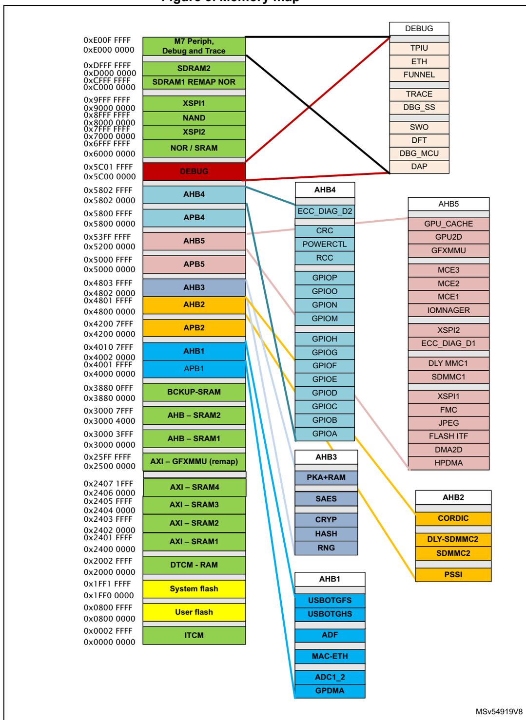
All the memory map areas that are not allocated to on-chip memories and peripherals are considered “Reserved”. For the detailed mapping of available memory and register areas, refer to the following table.
The following tables gives, the default memory attribute and the boundary addresses of the peripherals available in the devices.
Table 6. Memory map and default device memory area attribute
| Region | Boundary address | Arm® Cortex®-M7 | Type | Attributes | Execute never |
|---|---|---|---|---|---|
| External Devices | 0xD0000000 - 0xDFFFFFFF | Bank 2 | Device | - | Yes |
| 0xC0000000 - 0xCFFFFFFF | FMC SDRAM Bank1 (or remap FMC NOR/PSRAM/SRAM 1/2 Bank1) | ||||
| 0xBFF00000 - 0xBFFFFFFF | GPV/AXIM | ||||
| 0xA0000000 - 0xBFF00000 | Reserved | ||||
| External Memories | 0x90000000 - 0x9FFFFFFF | XSPI1 | Normal | Write-through cache attribute | No |
| 0x80000000 - 0x8FFFFFFF | FMC NAND Flash memory | Write-back, write allocate cache attribute | |||
| 0x70000000 - 0x7FFFFFFF | XSPI2 | ||||
| 0x60000000 - 0x6FFFFFFF | FMC NOR/PSRAM/SRAM 1 Bank1 (or remap of FMC SDRAM Bank1) | ||||
| Peripherals | 0x40000000 - 0x5FFFFFFF | Peripherals. See Table 7: Register boundary addresses . | Device | - | Yes |
| RAM | 0x38801000 - 0x3FFFFFFF | Reserved | Normal | Write-back, write allocate cache attribute | No |
| 0x38800000 - 0x38800FFF | Backup SRAM | ||||
| 0x38008000 - 0x387FFFFF | Reserved | ||||
| 0x30004000 - 0x30007FFF | SRAM2 | ||||
| 0x30000000 - 0x30003FFF | SRAM1 | ||||
| 0x2600 0000 - 0x2FFF FFFF | Reserved | ||||
| 0x2500 0000 - 0x25FF FFFF | AXI -SRAM GFXMMU | ||||
| 0x2407 2000 - 0x24FF FFFF | Reserved | ||||
| 0x24060000 - 0x24071FFF | AXI SRAM shared with ECC | ||||
| 0x24040000 - 0x2405FFFF | AXI SRAM shared with DTCM | ||||
| 0x24020000 - 0x2403FFFF | AXI SRAM | ||||
| 0x24000000 - 0x2401FFFF | AXI SRAM shared with ITCM | ||||
| 0x20030000 - 0x23FFFFFF | Reserved | ||||
| 0x20000000 - 0x2002FFFF | DTCM - RAM | ||||
Table 6. Memory map and default device memory area attribute
| Region | Boundary address | Arm® Cortex®-M7 | Type | Attributes | Execute never |
|---|---|---|---|---|---|
| Code | 0x1FF20000 - 0x1FFFFFFF | Reserved | Normal | Write-through cache attribute | No |
| 0x1FF00000 - 0x1FF1FFFF | System flash memory | ||||
| 0x90000000 - 0x1FEFFFFF | Reserved | ||||
| 0x08FFF800 - 0x08FFFFFF | Flash Read Only (ID, Trim, Stack ID) | ||||
| 0x08FFF400 - 0x08FFF7FF | Reserved | ||||
| 0x08FF0000 - 0x08FFF3FF | User OTP (Flash) | ||||
| 0x08010000 - 0x08FEFFFF | Reserved | ||||
| 0x08000000 - 0x0800FFFF | User flash memory bank 1 | ||||
| 0x00010000 - 0x07FFFFFF | Reserved | ||||
| 0x00000000 - 0x0002FFFF | ITCM RAM |
| Boundary address | Peripheral | Bus | Registers |
|---|---|---|---|
| 0x58028000 - 0x5BFFFFFF | Reserved | AHB4 | Reserved |
| 0x58027000 - 0x58027FFF | ECC_DIAG_D2 | RAMECC registers | |
| 0x58025000 - 0x58026FFF | Reserved | Reserved | |
| 0x58024C00 - 0x58024FFF | CRC | CRC registers | |
| 0x58024800 - 0x58024BFF | PWR | PWR registers | |
| 0x58024400 - 0x580247FF | RCC | RCC registers | |
| 0x58024000 - 0x580243FF | Reserved | Reserved | |
| 0x58023C00 - 0x58023FFF | GPIOI | GPIO registers | |
| 0x58023800 - 0x58023BFF | GPIOO | ||
| 0x58023400 - 0x580237FF | GPIOQ | ||
| 0x58023000 - 0x580233FF | GPIOI | ||
| 0x58022000 - 0x58022FFF | Reserved | Reserved | |
| 0x58021C00 - 0x58021FFF | GPIOH | GPIO registers | |
| 0x58021800 - 0x58021BFF | GPIOG | ||
| 0x58021400 - 0x580217FF | GPIOF | ||
| 0x58021000 - 0x580213FF | GPIOE | ||
| 0x58020C00 - 0x58020FFF | GPIOI | ||
| 0x58020800 - 0x58020BFF | GPIOC | ||
| 0x58020400 - 0x580207FF | GPIOB | ||
| 0x58020000 - 0x580203FF | GPIOA |
| Boundary address | Peripheral | Bus | Registers |
|---|---|---|---|
| 0x58006C00 - 0x5801FFFF | Reserved | Reserved | |
| 0x58006800 - 0x58006BFF | DTS | DTS registers | |
| 0x58004C00 - 0x580067FF | Reserved | Reserved | |
| 0x58004800 - 0x58004BFF | IWDG | IWDG registers | |
| 0x58004400 - 0x580047FF | TAMP | TAMP registers | |
| 0x58004000 - 0x580043FF | RTC | RTC registers | |
| 0x58003C00 - 0x58003FFF | VREFBUF | VREFBUF registers | |
| 0x58003400 - 0x58003BFF | Reserved | Reserved | |
| 0x58003000 - 0x580033FF | LPTIM5 | ||
| 0x58002C00 - 0x58002FFF | LPTIM4 | APB4 | LPTIM registers |
| 0x58002800 - 0x58002BFF | LPTIM3 | ||
| 0x58002400 - 0x580027FF | LPTIM2 | ||
| 0x58001800 - 0x580023FF | Reserved | ||
| 0x58001400 - 0x580017FF | SPI2S6 | SPI/I2S registers | |
| 0x58001000 - 0x580013FF | Reserved | Reserved | |
| 0x58000C00 - 0x58000FFF | LPUART1 | LPUART registers | |
| 0x58000800 - 0x58000BFF | Reserved | Reserved | |
| 0x58000400 - 0x580007FF | SBS | SBS registers | |
| 0x58000000 - 0x580003FF | EXTI | EXTI registers | |
| 0x54000FFF - 0x57FFFF | Reserved | - | Reserved |
| Boundary address | Peripheral | Bus | Registers |
|---|---|---|---|
| 0x52015400 - 0x53FFFFFF | Reserved | AHB5 | Reserved |
| 0x52015000 - 0x520153FF | ICACHE | ICACHE registers | |
| 0x52014000 - 0x52014FFF | GPU2D | Reserved | |
| 0x52010000 - 0x52013FFF | GFXMMU | GFXMMU registers | |
| 0x5200C400 - 0x5200CFFF | Reserved | Reserved | |
| 0x5200C000 - 0x520003FF | MCE3 | MCE registers | |
| 0x5200BC00 - 0x5200BFFF | MCE2 | ||
| 0x5200B800 - 0x5200BBFF | MCE1 | ||
| 0x5200B400 - 0x5200B7FF | XSPIM1 | XSPIM registers | |
| 0x5200B000 - 0x5200B3FF | Reserved | Reserved | |
| 0x5200A000 - 0x5200AFFF | XSPI2 | XSPI registers | |
| 0x52009000 - 0x52009FFF | ECC DIAG_D1 | RAMECC registers | |
| 0x52008400 - 0x52008FFF | Reserved | Reserved | |
| 0x52008000 - 0x520083FF | DLYB SDMMC1 | DLYB registers | |
| 0x52007000 - 0x52007FFF | SDMMC1 | SDMMC registers | |
| 0x52006000 - 0x52006FFF | Reserved | Reserved | |
| 0x52005000 - 0x52005FFF | XSPI1 | XSPI registers | |
| 0x52004000 - 0x52004FFF | FMC | FMC register map | |
| 0x52003000 - 0x52003FFF | JPEG | JPEG codec registers | |
| 0x52002000 - 0x52002FFF | FLASH | FLASH registers | |
| 0x52001000 - 0x52001FFF | DMA2D | DMA2D registers | |
| 0x52000000 - 0x52000FFF | HPDMA1 | HPDMA registers | |
| 0x50010000 - 0x51FFFFFF | Reserved | Reserved | Reserved |
| 0x50004400 - 0x5000FFFF | Reserved | APB5 | Reserved |
| 0x50004000 - 0x500043FF | GFXTIM | GFXTIM registers | |
| 0x50002400 - 0x50003FFF | Reserved | Reserved | |
| 0x50002000 - 0x500023FF | DCMIPP | DCMIPP registers | |
| 0x50001400 - 0x50001FFF | Reserved | Reserved | |
| 0x50001000 - 0x500013FF | LTDC | LTDC registers | |
| 0x50000000 - 0x50000FFF | Reserved | Reserved | |
| 0x48004000 - 0x4FFFFFFF | Reserved | Reserved | Reserved |
| Boundary address | Peripheral | Bus | Registers |
|---|---|---|---|
| 0x48024000 - 0x4803FFFF | Reserved | AHB3 | Reserved |
| 0x48022000 - 0x48023FFF | PKA+RAM | PKA registers | |
| 0x48021400 - 0x48021FFF | Reserved | Reserved | |
| 0x48021000 - 0x480213FF | SAES | SAES | |
| 0x48020C00 - 0x48020FFF | Reserved | Reserved | |
| 0x48020800 - 0x48020BFF | CRYP | CRYP registers | |
| 0x48020400 - 0x480207FF | HASH | HASH registers | |
| 0x48020000 - 0x480203FF | RNG | RNG registers | |
| 0x48004800 - 0x4801FFFF | Reserved | AHB2 | Reserved |
| 0x48004400 - 0x480047FF | CORDIC | CORDIC registers | |
| 0x48002C00 - 0x480043FF | Reserved | Reserved | |
| 0x48002800 - 0x48002BFF | DLYB SDMMC2 | DLYB registers | |
| 0x48002400 - 0x480027FF | SDMMC2 | SDMMC registers | |
| 0x48000800 - 0x48000BFF | Reserved | Reserved | |
| 0x48000400 - 0x480007FF | PSSI | PSSI registers | |
| 0x48000000 - 0x480003FF | Reserved | Reserved | |
| 0x42006000 - 0x47FFFFFF | Reserved | APB2 | Reserved |
| 0x42005C00 - 0x42005FFF | SAI2 | SAI registers | |
| 0x42005800 - 0x42005BFF | SAI1 | ||
| 0x42005400 - 0x420057FF | Reserved | Reserved | |
| 0x42005000 - 0x420053FF | SPI5 | SPI/I2S registers | |
| 0x42004C00 - 0x42004FFF | TIM9 | TIM9/TIM12 registers (shared with TIM9) | |
| 0x42004800 - 0x42004BFF | TIM17 | TIM15 registers | |
| 0x42004400 - 0x420047FF | TIM16 (16b) | ||
| 0x42004000 - 0x420043FF | TIM15 (16b) | SPI/I2S registers | |
| 0x42003800 - 0x42003FFF | Reserved | ||
| 0x42003400 - 0x420037FF | SPI4 | USART registers | |
| 0x42003000 - 0x420033FF | SPI2S1 | ||
| 0x42002800 - 0x42002BFF | Reserved | Reserved | |
| 0x42002400 - 0x420027FF | Reserved | TIM1 registers | |
| 0x42002000 - 0x420023FF | USART1 | ||
| 0x42001800 - 0x42001BFF | Reserved | Reserved | |
| 0x42001400 - 0x420017FF | Reserved | TIM1 registers | |
| 0x42001000 - 0x420013FF | USART1 | ||
| 0x42000800 - 0x42000BFF | Reserved | Reserved | |
| 0x42000400 - 0x420007FF | Reserved | TIM1 registers | |
| 0x42000000 - 0x420003FF | TIM1 (16b) |
| Boundary address | Peripheral | Bus | Registers |
|---|---|---|---|
| 0x400C0000 - 0x41FFFFFF | Reserved | AHB1 | Reserved |
| 0x40080000 - 0x400BFFFF | OTG FS | OTG_FS registers | |
| 0x40040000 - 0x4007FFFF | OTG HS | OTG_HS registers | |
| 0x40030000 - 0x4003FFFF | Reserved | Reserved | |
| 0x4002F000 - 0x4002FFFF | ADF& | ADF registers | |
| 0x40029400 - 0x40022EFF | Reserved | Reserved | |
| 0x40028000 - 0x400293FF | ETH1 | Ethernet registers | |
| 0x40022400 - 0x40027FFF | Reserved | Reserved | |
| 0x40022000 - 0x400223FF | ADC1/ADC2 | ADC registers (for each ADC) | |
| 0x40021000 - 0x40021FFF | GPDMA1 | GPDMA registers | |
| 0x40020000 - 0x40020FFF | Reserved | Reserved |
| Boundary address | Peripheral | Bus | Registers |
|---|---|---|---|
| 0x4000F000 - 0x4001FFFF | Reserved | APB1 | Reserved |
| 0x4000EC00 - 0x4000EFFF | UCPD1 | UCPD registers | |
| 0x4000B400 - 0x4000EBFF | Reserved | Reserved | |
| 0x4000AC00 - 0x4000B3FF | CAN Msg RAM | FDCAN registers | |
| 0x4000A800 - 0x4000ABFF | Reserved | Reserved | |
| 0x4000A400 - 0x4000A7FF | FDCAN2 | FDCAN registers | |
| 0x4000A000 - 0x4000A3FF | FDCAN1 | ||
| 0x40009800 - 0x40009FFF | Reserved | Reserved | |
| 0x40009400 - 0x400097FF | MDIOS | MDIOS registers | |
| 0x40008800 - 0x400093FF | Reserved | Reserved | |
| 0x40008400 - 0x400087FF | CRS | CRS registers | |
| 0x40008000 - 0x400083FF | Reserved | Reserved | |
| 0x40007C00 - 0x40007FFF | UART8 | USART registers | |
| 0x40007800 - 0x40007BFF | UART7 | ||
| 0x40007000 - 0x400077FF | Reserved | Reserved | |
| 0x40006C00 - 0x40006FFF | CEC | HDMI-CEC registers | |
| 0x40006000 - 0x40006BFF | Reserved | Reserved | |
| 0x40005C00 - 0x40005FFF | I2C3 | I2C registers I3C registers | |
| 0x40005800 - 0x40005BFF | I2C2 | ||
| 0x40005400 - 0x400057FF | I2C1/I3C1 | USART registers | |
| 0x40005000 - 0x400053FF | UART5 | ||
| 0x40004C00 - 0x40004FFF | UART4 | ||
| 0x40004800 - 0x40004BFF | USART3 | ||
| 0x40004400 - 0x400047FF | USART2 | ||
| 0x40004000 - 0x400043FF | SPDIFRX1 | SPDIFRX interface registers | |
| 0x40003C00 - 0x40003FFF | SPI2S3 | SPI/I2S registers | |
| 0x40003800 - 0x40003BFF | SPI2S2 | ||
| 0x40003000 - 0x400037FF | Reserved | Reserved | |
| 0x40002C00 - 0x40002FFF | WWATCHDOG | WWDG registers | |
| 0x40002800 - 0x40002BFF | Reserved | Reserved | |
| 0x40002400 - 0x400027FF | LPTIM1 | LPTIM registers | |
| 0x40002000 - 0x400023FF | TIM14 (Light) | TIM9/TIM12 registers | |
| 0x40001C00 - 0x40001FFF | TIM13 (Light) | ||
| 0x40001800 - 0x40001BFF | TIM12 (Light) | ||
| 0x40001400 - 0x400017FF | TIM7 (Basic) | TIM6/TIM7 registers |
| Boundary address | Peripheral | Bus | Registers |
|---|---|---|---|
| 0x40001000 - 0x400013FF | TIM6 (Basic) | APB1 | TIM6/TIM7 registers |
| 0x40000C00 - 0x40000FFF | TIM5 (32b) | TIM2/TIM3/TIM4/TIM5 registers | |
| 0x40000800 - 0x40000BFF | TIM4 (32b) | ||
| 0x40000400 - 0x400007FF | TIM3 (32b) | ||
| 0x40000000 - 0x400003FF | TIM2 (32b) |
1. Accessing a reserved area results in a bus error. Accessing undefined memory space in a peripheral returns zeros.
2.4 Embedded SRAM
The STM32H7Rx/7Sx devices include up to 456 Kbytes of AXI-SRAM mapped onto the AXI bus divided and shared as described in the following section.
- • Up to 192 Kbytes of instruction TCM RAM Table 9: SRAM1 / ITCM configurations . This feature can be configured through the ITCM_AXI_SHARE[1:0] option byte in FLASH_OBW2SRP register as described in the FLASH option byte word 2 status register (FLASH_OBW2SR)
- • Up to 192 Kbytes of data TCM RAM Table 10: SRAM3 / DTCM configurations . This feature can be configured through the DTCM_AXI_SHARE[1:0] option byte in described in the FLASH option byte word 2 status register (FLASH_OBW2SR) .
- • Up to 72 Kbytes when ECC is disabled Table 11: SRAM4 / ECC configurations . This feature can be configured through the ECC_ON_SRAM option byte in FLASH_OBW2SRP register as described in the FLASH option byte word 2 status register (FLASH_OBW2SR) .
- • 16 Kbyte AHB_SRAM1
- • 16 Kbyte AHB_SRAM2
The system AHB SRAM can be accessed as bytes, half-words (16-bit units) or words (32-bit units), while the system AXI SRAM can be accessed as bytes, half-words, words or double-words (64-bit units). These memories can be addressed at maximum system clock frequency without wait state.
The AHB masters can read/write-access an SRAM section concurrently with the Ethernet MAC or the USB OTG HS peripheral accessing another SRAM section. For example, the Ethernet MAC accesses the SRAM2 while the CPU accesses the SRAM1, concurrently.
The TCM SRAMs are dedicated to the Cortex ® -M7:
- • DTCM-RAM on TCM interface is mapped at the address 0x2000 0000 and accessible by Cortex ® -M7, and by HPDMA through AHBS slave bus of the Cortex ® -M7 CPU. The DTCM-RAM can be used as read-write segment to host critical real-time data (such as stack and heap) for application running on Cortex ® -M7 CPU.
- • ITCM-RAM on TCM interface mapped at the address 0x0000 0000 and accessible by Cortex ® -M7 and by HPDMA through AHBS slave bus of the Cortex ® -M7 CPU. The ITCM-RAM can be used to host code for time-critical routines (such as interrupt handlers) that requires deterministic execution.
The backup RAM is mapped at the address 0x3880 0000 and is accessible by most of the system masters. With a battery connected to the V BAT pin, the backup SRAM can be used to retain data during low-power mode (Standby and V BAT mode).
These SRAMs are made of several blocks that are maintained but not usable in Stop mode (AXI SRAM) :
- • AXI SRAM
- – SRAM1is splitted in fix allocation and shared part depending on the user option byte define in
FLASH option byte word 2 status register (FLASH_OBW2SR)
.
1x64-Kbyte fix allocation + 2x64 Kbytes shared with the ITCM. - – SRAM2: 128-Kbytes not shared (no ECC).
- – SRAM3: 128-Kbytes shared by block of 64-Kbytes with DTCM0 and DTCM1. when shared the same amount is affected to each DTCM per 32-Kbytes each. The amount of memory allocated to each DTCM is define in FLASH option byte word 2 status register (FLASH_OBW2SR) .
- – SRAM4: 72-Kbyte (no ECC) comming from SRAM1 (24-Kbytes) and SRAM3 (48-Kbytes) when ECC is disabled FLASH option byte word 2 status register (FLASH_OBW2SR)
- – SRAM1is splitted in fix allocation and shared part depending on the user option byte define in
FLASH option byte word 2 status register (FLASH_OBW2SR)
.
- • backup SRAM
- – The backup SRAM (BKPSRAM) can be retained in all low-power modes and when \( V_{DD} \) is off in \( V_{BAT} \) mode. Refer to Section 6.4.4: Backup domain for more details. The backup SRAM is protected by the tamper detection circuit, and are erased by hardware in case of tamper detection. They are also erased by hardware in case of a Backup domain reset. Refer to (link to Section 50: Tamper and backup registers (TAMP) ) for more details.
The tables below summarize the different configuration supported by each internal SRAM:
Table 8. SRAMs structure
| SRAM | STM32H7Rx/7Sx |
|---|---|
| SRAM1 | From 0 to 128 Kbytes, shared with ITCM |
| SRAM2 | 128 Kbytes no ECC |
| SRAM3 | From 0 up to 128 Kbytes, shared with DTCM0/1 |
| SRAM4 | From 0 to 72 Kbytes, shared with ECC |
| AHB SRAM1/2 | 16 Kbytes, AHB domain |
| BKPSRAM | 4 Kbytes |
Table 9. SRAM1 / ITCM configurations
| Allocation | SRAM1 / ITCM split (Kbytes) | ||
|---|---|---|---|
| 0 | 64 | 128 | |
| SRAM1 allocation | 0 | 64 | 128 |
| ITCM allocation | 192 | 128 | 64 |
Table 10. SRAM3 / DTCM configurations
| Allocation | SRAM3 / DTCM split (Kbytes) | ||
|---|---|---|---|
| 0 | 64 | 128 | |
| SRAM3 allocation | 0 | 64 | 128 |
| DTCM0 allocation | 96 | 64 | 32 |
| DTCM1 allocation | 96 | 64 | 32 |
Table 11. SRAM4 / ECC configurations
| ECC | SRAM4 allocation (Kbytes) |
|---|---|
| ON | 0 |
| OFF | 72 |
RAM shared between TCM and AXI RAM
128 Kbyte of RAM (SRAM1 for ITCM, SRAM3 for DTCM) can be used either as TCM or as AXI SRAM. This feature can be configured through the ITCM_AXI_SHARED[1:0] and DTCM_AXI_SHARED[1:0] option byte in FLASH_OBW2SRP register, in Section 5: Embedded flash memory (FLASH) , as described in Table 12 and Table 14
Table 12. ITCM/AXI configuration
| ITCM_AXI_SHARED[1,0] | ITCM size (Kbyte) | ITCM memory mapping (1) | AXI size (Kbyte) | AXI SRAM1 memory mapping (2) |
|---|---|---|---|---|
| 00/11 | 64 | 0x00000 0000 - 0x0000 FFFF | 128 | 0x2400 0000 - 0x2401 FFFF |
| 01 | 128 | 0x0000 0000 - 0x0001 FFFF | 64 | 0x2401 0000 - 0x2401 FFFF |
| 10 | 192 | 0x0000 0000 - 0x0002 FFFF | 0 | - |
- 1. Access to an unmapped area gives a TCM error.
- 2. Access to an unmapped area gives a bus error.
Table 13. DTCM/AXI configuration
| DTCM_AXI_SHARED[1,0] | DTCM size (Kbyte) | DTCM memory mapping (1) | AXI size (Kbyte) | AXI SRAM3 memory mapping (2) |
|---|---|---|---|---|
| 00/11 | 64 | 0x2000 0000 - 0x2000 FFFF | 128 | 0x2404 0000 - 0x2405 FFFF |
| 01 | 128 | 0x2000 0000 - 0x2001 FFFF | 64 | 0x2404 0000 - 0x2404 FFFF |
| 10 | 192 | 0x2000 0000 - 0x2002 FFFF | 0 | - |
- 1. Access to an unmapped area gives a TCM error.
- 2. Access to an unmapped area gives a bus error.
RAM shared between ECC and AXI RAM
72 Kbyte of RAM (SRAM4 ) can be used either by ECC or as AXI SRAM. This feature can be configured through the ECC_ON_SRAM option byte in FLASH_OBW2SRP register as described in Table 14 .
Table 14. ECC/AXI configuration
| ECC_ON_SRAM | AXI size (Kbytes) | AXI SRAM4 memory mapping (1) |
|---|---|---|
| 0 | 72 | 0x2406 0000 - 0x2407 1FFF |
| 1 | 0 | - |
- 1. Access to an unmapped area gives a bus error.
Refer to Section 5: Embedded flash memory (FLASH) for a description of the ECC_ON_SRAM option byte.
2.5 Flash memory overview
The Flash memory interface manages accesses to the Flash memory. It implements the erase and program Flash memory operations and the read and write protection mechanisms.
The Flash memory is organized as follows:
- • A main memory block divided into sectors.
- • An information block:
- – System memory from which the device boots in System memory boot mode
- – Option bytes to configure read and write protection, BOR level, watchdog software/hardware and reset when the device is in Standby or Stop mode.
Refer to Section 5: Embedded flash memory (FLASH) for further details.
2.6 Boot configuration
In the STM32H7Rx/7Sx, two different boot areas can be selected through the BOOT0 pin as shown in the Table 15 .
Table 15. Boot modes
| Boot mode selection | Boot area | |||
|---|---|---|---|---|
| PRODUCT_STATE | NVSTATE | BOOT0 | IROT_SELECT (1) | |
| Open | OPEN | 0 | - | Boot from the user flash memory at 0x0800 0000 |
| 1 | Boot from the bootloader | |||
| Provisioning | CLOSE | - | Not 0xB4 or H7R | Boot from the RSS in system flash memory Then jump into the bootloader |
| Closed/Locked | Boot from the RSS in system flash memory Then jump into the user flash memory at 0x0800 0000 (2) | |||
| Closed/Locked | 0xB4 | Boot from the RSS in system flash memory Then jump into the ST iRoT in system flash memory | ||
1. IROT_SELECT is relevant only on H7S.
2. MPU is enabled when executing OEM FW in user flash memory; depending on needed resources, OEM FW should update MPU configuration or disable MPU.
The values on the BOOT0 pin are latched on the 4th rising edge of SYSCLK after reset release. It is up to the user to set the BOOT0 pin after reset.
The BOOT0 pin is re-sampled when the device exits Standby mode. Consequently, the values must be kept in the required Boot mode configuration when the device is in Standby mode.
After startup delay, the selection of the boot area is done before releasing the processor reset.
Embedded bootloader
The embedded bootloader code is located in system memory. It is programmed by ST during production. It is used to reprogram the flash memory using one of the following serial interfaces:
- • DFU: USB OTG FS (PM12/PM11) in device mode
- • USART1: PA10/PA9
- • USART2: PA3/PA2
- • USART3: PD9/PD8
- • UART4: PD0/PD1
- • FDCAN2: PB5/PB1
- • I2C1: PB8/PB7
- • I2C2: PB10/PB11
- • I2C3: PA8/PC9
- • I3C1: PB8/PB7
- • SPI1: PA4/PA5/PA6/PA7
- • SPI2: PB15/PB14/PB13/PB12
- • SPI3: PC12/PB4/PB3/PA15
For additional information, refer to Section 8: System configuration, boot and security (SBS) on page 540 .