33. Debug support (DBG)
33.1 Introduction
A comprehensive set of debug features is provided to support software development and system integration:
- • Independent breakpoint debugging of each CPU core in the system
- • Code execution tracing
- • Software instrumentation
- • Cross-triggering
- • The debug features can be controlled via a JTAG/Serial-wire debug access port, using industry standard debugging tools. A trace port allows data to be captured for logging and analysis.
The debug features are based on Arm ® CoreSight ™ components.
- • General features:
- – SWJ-DP: JTAG/Serial-wire debug port
- – AHB-AP: AHB access port
- • CPU2 debug features:
- – ROM tables
- – System control space (SCS)
- – Breakpoint unit (BPU)
- – Data watchpoint and Trace unit (DWT)
- – Cross trigger interface (CTI)
- • CPU1 debug features:
- – ROM table
- – System control space (SCS)
- – Breakpoint unit (FPB)
- – Data watchpoint and Trace unit (DWT)
- – Instrumentation trace macrocell (ITM)
- – Cross trigger interface (CTI)
- – Trace port interface unit (TPU)
CPU2 debug access via CPU2 AHB-AP and its associated AHB bus is disabled.
The CPU1 debug features are accessible by the debugger via the CPU1 AHB-AP.
Additional information can be found in the Arm ® documents referenced in Section 33.19 .
33.2 Debug use cases
The trace and debug system is designed to support a variety of typical use cases:
- • Low cost trace
Limited trace capability is available over the single-wire debug output. This supports code instrumentation using “printf”, tracing of data and address watchpoints, interrupt
detection and program counter sampling. Single-wire trace can be maintained even when one or both processors are switched off or clock-stopped.
- • Breakpoint debugging of each core independently
Both processor cores can be simultaneously and independently debugged using equipment connected to the JTAG/SWD debug port. This enables, among others, breakpoint and watchpoint setting, code stepping and memory access. - • Synchronous debugging of both cores
When one core stops due to a breakpoint or a debugger stop command, the other core can be stopped as well. Similarly, the cores can be restarted at the same time. This allows the user to debug loosely coupled applications, which require the processors to remain synchronized. - • Tracing code execution via the trace port
Trace information from the CPU1 (Cortex®-M4) is combined into a single trace stream and sent to a trace port analyzer in real time. An ID embedded in the trace allows the analyzer to identify the source of each information packet.
33.3 DBG functional description
33.3.1 DBG block diagram
Figure 313. Block diagram of debug support infrastructure
The diagram illustrates the debug support infrastructure for a dual-core system. On the left, the JTAG/Serial Wire port includes pins for JTMS/SWDIO, JTDI, JTDO/TRACESWO, JTCK/SWCLK, and nJTRST. These connect to a Debug Access Port (DAP) containing an SWJ-DP 1 component. The DAP is connected via a DAPBUS to an AHB-AP 1 . The AHB-AP 1 is connected to the AHB bus. The AHB bus connects to CPU1 Cortex ® -M4 and CPU2 Cortex ® -M0+ . CPU1 contains components: DWT 1 , FPB 1 , ITM 1 , TPIU 1 , Core , ROM table 1 , ETM 1 , and CTI 1 . CPU2 contains components: ROM1 table 1 , ROM2 table 1 , Core , BPU 1 , and DWT 1 . A CTI 1 component is shared between the CPUs, connected via CTM . A DBG_MCU is also connected to the CTI 1 and CTM . On the right, the Trace port includes pins for TRACECLK and TRACEDATA[3:0].
1. Arm ® CoreSight ™ component
33.3.2 DBG pins and internal signals
Table 204. JTAG/Serial-wire debug port pins
| Pin name | JTAG debug port | SW debug port | Pin assignment | ||
|---|---|---|---|---|---|
| Type | Description | Type | Description | ||
| JTMS/SWDIO | I | JTAG test mode select | IO | Serial wire data in/out | PA13 |
| JTCK/SWCLK | I | JTAG test clock | I | Serial wire clock | PA14 |
| JTDI | I | JTAG test data input | - | - | PA15 |
| JTDO/TRACESWO | O | JTAG test data output | - | - | PB3 |
| nJTRST | I | JTAG test reset | - | - | PB4 |
| Pin name | Type | Description | Pin assignment |
|---|---|---|---|
| TRACED0 | O | Trace synchronous data out 0 | Refer to datasheet |
| TRACED1 | Trace synchronous data out 1 | ||
| TRACED2 | Trace synchronous data out 2 | ||
| TRACED3 | Trace synchronous data out 3 | ||
| TRACECK | Trace clock |
| Pin name | Type | Description | Pin assignment |
|---|---|---|---|
| TRACESWO | O | Single wire trace asynchronous data out | PB3 (1) |
- 1. TRACESWO is multiplexed with JTDO. This means that single wire trace is only available when using the serial wire debug interface, and not when using JTAG.
| Pin name | Type | Description | Pin assignment |
|---|---|---|---|
| TRIG_INOUT | IO | External trigger bi-directional (1) | Refer to datasheet |
- 1. TRIG_INOUT can be configured as an input or an output by the TRGOEN bit in the DBGMCU.
33.3.3 DBG power domains
The debug components are located in the core power domain. This means that debugger connection is not possible in shutdown or standby low power modes. To avoid losing the connection when the device enters standby mode, it is possible to maintain the power to the core by setting a bit in the DBGMCU. This keeps the processor clocks active, and holds off the reset, so that the debug session is maintained.
33.3.4 DBG clocks
The debugger supplies the clock for the debug port via the debug interface pin, JTCK/SWCLK. This clock is used to register the serial input data in both serial wire and JTAG mode, as well as to operate the state machines and internal logic of the debug port. It must therefore continue to toggle for several cycles after the end of an access, to ensure that the debug port returns to the idle state.
The SWJ-DP contains an asynchronous interface to the DAPCLK domain, which covers the rest of the SWJ-DP and the CPU2 access port.
The DAPCLK is a gated version of the system HCLK4.
The DAPCLK domain is enabled by the debugger using the CDBGPWRUPREQ bit in the debug port CTRL/STAT register. The clock must be enabled before the debugger can access any of the debug features on the device. The availability of the clock is reflected in the CDBGPWRUPACK bit in the debug port CTRL/STAT register. The DAPCLK is disabled at power up, after OBL, and after wakeup from Standby, and must be disabled when the debugger is disconnected, to reduce power consumption.
The debug and trace components included in the processors (among them ITM, DWG, FPB) are clocked with the corresponding core clock.
33.3.5 Debug and low power modes
The devices include power saving features that allow the core power domain to be switched off or stopped when not required. If the power is switched off, or the core is not clocked, all debug components are inaccessible to the debugger. To avoid this, power saving mode emulation has been implemented. If emulation is enabled for a domain, the domain still enters power saving mode, but its clock and power are maintained. In other words, the domain behaves as if it is in power saving mode, but the debugger does not lose the connection.
Emulation mode is programmed in the microcontroller debug (DBGMCU) unit. For more information refer to Section 33.8 .
33.3.6 DBG reset
The debug port (SWJ-DP) is reset by a power-on reset or an OBL reset, and when waking up from Standby mode.
33.4 Serial wire and JTAG debug port (SWJ-DP)
The SWJ-DP is a Coresight™ component that implements an external access port for connecting debugging equipment.
Two types of interface can be configured:
- – a 5-pin standard JTAG interface (JTAG-DP)
- – a 2-pin (clock + data) “serial-wire debug” port (SW-DP)
The two modes are mutually exclusive, since they share the same IO pins.
By default the JTAG-DP is selected after a system or a power-on reset. The five IO pins are configured by hardware in debug alternative function mode. The SWJ-DP incorporates pull-up resistors on JTDI, JTMS/SWDIO, and nJTRST, as well as a pull-down resistor on JTCK/SWCLK.
A debugger can select the SW-DP by transmitting the following serial data sequence on JTMS/SWDIO:
... (50 or more ones) ..., 0, 1, 1, 1, 1, 0, 0, 1, 1, 1, 1, 0, 0, 1, 1, 1, ... (50 or more ones) ...
JTCK/SWCLK must be cycled for each data bit.
In SW-DP mode, the unused JTAG pins JTDI, JTDO and nJTRST can be used for other functions. It should be noted that all SWJ port IOs can be reconfigured to other functions by software, but debugging is no longer possible.
33.4.1 JTAG debug port
There are two TAPs on the JTAG debug port, the JTAG-DP TAP and the BSC TAP.
The JTAG-DP implements a TAP state machine (TAPSM), shown in Figure 314 , based on IEEE Std 1149.1-1990. The state machine controls two scan chains, one associated with an instruction register (IR), and the other one with a number of data registers (DR).
Figure 314. JTAG TAP state machine
stateDiagram-v2
    [*] --> Test-Logic-Reset
    Test-Logic-Reset --> Run-Test/Idle : JTMS=0
    Run-Test/Idle --> Select-DR-Scan : JTMS=1
    Run-Test/Idle --> Select-IR-Scan : JTMS=1
    Select-DR-Scan --> Capture-DR : JTMS=0
    Select-IR-Scan --> Capture-IR : JTMS=0
    Capture-DR --> Shift-DR : JTMS=0
    Capture-IR --> Shift-IR : JTMS=0
    Shift-DR --> Exit1-DR : JTMS=1
    Shift-IR --> Exit1-IR : JTMS=1
    Exit1-DR --> Pause-DR : JTMS=0
    Exit1-IR --> Pause-IR : JTMS=0
    Pause-DR --> Exit2-DR : JTMS=1
    Pause-IR --> Exit2-IR : JTMS=1
    Exit2-DR --> Update-DR : JTMS=1
    Exit2-IR --> Update-IR : JTMS=1
    Update-DR --> Run-Test/Idle : JTMS=0
    Update-IR --> Run-Test/Idle : JTMS=0
    Update-DR --> Select-DR-Scan : JTMS=1
    Update-IR --> Select-IR-Scan : JTMS=1
    Update-DR --> Select-IR-Scan : JTMS=1
    Update-IR --> Select-DR-Scan : JTMS=1
The operation of the JTAG-DP is as follows:
- • When the TAPSM goes through the Capture-IR state, 0b0001 is transferred onto the Instruction register (IR) scan chain. The IR scan chain is connected between JTDI and JTDO.
- • While the TAPSM is in the Shift-IR state, the IR scan chain shifts one bit for each rising edge of JTCK. This means that on the first tick:
- – The LSB of the IR scan chain is output on JTDO.
- – Bit[n] of the IR scan chain is transferred to bit[n-1].
- – The value on JTDI is transferred to the MSB of the IR scan chain.
- • When the TAPSM goes through the Update-IR state, the value scanned into the IR scan chain is transferred into the Instruction register.
- • When the TAPSM goes through the Capture-DR state, a value is transferred from one
of the Data registers onto one of the DR scan chains, connected between JTDI and JTDO.
- • The value held in the Instruction register determines which Data register (and associated DR scan chain) is selected.
- • This data is then shifted while the TAPSM is in the Shift-DR state, in the same manner as the IR shift in the Shift-IR state.
- • When the TAPSM goes through the Update-DR state, the value scanned into the DR scan chain is transferred into the selected Data register.
- • When the TAPSM is in the Run-Test/Idle state, no special actions occur. The IDCODE instruction is loaded in IR.
When active, the nJTRST signal resets the state machine asynchronously to the Test-Logic-Reset state.
The data registers corresponding to the 4-bit IR instructions are listed in Table 208 . The total IR instruction length is 9 bits.
Table 208. JTAG-DP data registers
| IR instruction | DR register | Scan chain length | Description |
|---|---|---|---|
| 0000 to 0111 | (BYPASS) | 1 | Not implemented: BYPASS selected |
| 1000 | ABORT | 35 | ABORT register – Bits 31:1 = Reserved – Bit 0 = APABORT: write 1 to generate an AP abort. |
| 1001 | (BYPASS) | 1 | Reserved: BYPASS selected |
| 1010 | DPACC | 35 | Debug port access register Initiates the debug port and gives access to a debug port register. – When transferring data IN: Bits 34:3 = DATA[31:0] = 32-bit data to transfer for a write request Bits 2:1 = A[3:2] = 2-bit address of a debug port register. Bit 0 = RnW = Read request (1) or write request (0). – When transferring data OUT: Bits 34:3 = DATA[31:0] = 32-bit data read following a read request Bits 2:0 = ACK[2:0] = 3-bit Acknowledge: 010 = OK/FAULT 001 = WAIT OTHER = reserved |
| 1011 | APACC | 35 | Access port access register Initiates an access port and gives access to an access port register. – When transferring data IN: Bits 34:3 = DATA[31:0] = 32-bit data to shift in for a write request Bits 2:1 = A[3:2] = 2-bit sub-address of an access port register. Bit 0 = RnW = Read request (1) or write request (0). – When transferring data OUT: Bits 34:3 = DATA[31:0] = 32-bit data read following a read request Bits 2:0 = ACK[2:0] = 3-bit Acknowledge: 010 = OK/FAULT 001 = WAIT OTHER = reserved |
| 1100 | (BYPASS) | 1 | Reserved: BYPASS selected |
Table 208. JTAG-DP data registers (continued)
| IR instruction | DR register | Scan chain length | Description |
|---|---|---|---|
| 1101 | (BYPASS) | 1 | Reserved: BYPASS selected |
| 1110 | IDCODE | 32 | ID Code 0x6BA0 0477: Arm® JTAG debug port ID code |
| 1111 | BYPASS | 1 | Bypass A single JTC cycle delay is inserted between JTDI and JTDO |
The DR registers are described in more detail in the Arm® Debug Interface Architecture Specification [1].
33.4.2 SW debug port
The Serial Wire Debug protocol uses two pins:
- • SWCLK: clock from host to target
- • SWDIO: bi-directional serial data (100 kΩ pull-up required)
Serial data is transferred LSB first, synchronously with the clock. A transfer comprises three phases:
- 1. packet request (8 bits) transmitted by the host, see Table 209 .
- 2. acknowledge response (3 bits) transmitted by the target, see Table 210 .
- 3. data transfer (33 bits) transmitted by the host (in case of a write) or target (in case of a read), see Table 211 .
The data transfer only occurs if the acknowledge response is OK.
Between each phase, if the direction of the data is reversed, a single clock cycle turn-around time is inserted.
Table 209. Packet request
| Bit field | Name | Description |
|---|---|---|
| 0 | Start | Must be “1” |
| 1 | APnDP | – 0: DP register access - see
Table 208
for a list of DP registers – 1: AP register access - see Section 33.5: Access ports |
| 2 | RnW | – 0: Write request – 1: Read request |
| 4:3 | A(3:2) | Address field of the DP or AP register (refer to ) |
| 5 | Parity | Single bit parity of preceding bits |
| 6 | Stop | 0 |
| 7 | Park | Not driven by host, must be read as “1” by target |
| Bit field | Name | Description |
|---|---|---|
| 2:0 | ACK |
|
| Bit field | Name | Description |
|---|---|---|
| 31:0 | WDATA or RDATA | Write or Read data |
| 32 | Parity | Single bit parity of 32 data bits |
In the case of a FAULT or WAIT ACK response from the target, the data transfer phase is canceled, unless overrun detection is enabled: in this case the data is ignored by the target (in the case of a write), or not driven (in the case of a read).
A line reset must be generated by the host when it is first connected, or following a protocol error. The line reset consists in 50 or more SWCLK cycles with SWDIO high, followed by two SWCLK cycles with SWDIO low.
For more details on the Serial Wire debug protocol, refer to the Arm® Debug Interface Architecture Specification [1].
Note: The SWJ-DP implements SWD protocol version 2.
33.4.3 Debug port registers
Both the SW-DP and the JTAG-DP access the debug port (DP) registers listed in Table 212 .
The debugger can access the DP registers as follows:
- • Program the A(3:2) field in the DPACC register, if using JTAG, with the register address within the bank. Program the RnW bit to select a Read or Write. In the case of a write, program the DATA field with the write data. If using SWD, the A(3:2) and RnW fields are part of the Packet Request word sent to the SW-DP with the APnDP bit reset (see Table 209 ). The write data are sent in the data phase.
- • To access one of the banked DP registers at address 0x4, the register number must first be written to the DP_SELECT register at address 0x8. Any subsequent read or write to address 0x4 accesses the register corresponding to the content of the DP_SELECT register.
33.4.4 DP debug port identification register (DP_PIDR)
Address offset: 0x0
Reset value: 0x5BA0 2477
Read only
| 31 | 30 | 29 | 28 | 27 | 26 | 25 | 24 | 23 | 22 | 21 | 20 | 19 | 18 | 17 | 16 |
|---|---|---|---|---|---|---|---|---|---|---|---|---|---|---|---|
| REVISION[3:0] | PARTNO[7:0] | Res. | Res. | Res. | MIN | ||||||||||
| r | r | r | r | r | r | r | r | r | r | r | r | r | |||
| 15 | 14 | 13 | 12 | 11 | 10 | 9 | 8 | 7 | 6 | 5 | 4 | 3 | 2 | 1 | 0 |
| VERSION[3:0] | DESIGNER[10:0] | Res. | |||||||||||||
| r | r | r | r | r | r | r | r | r | r | r | r | r | r | r | |
Bits 31:28 REVISION[3:0] : Revision code
0x5
Bits 27:20 PARTNO[7:0] : Part number for the debug port
0xBA
Bits 19:17 Reserved, must be kept at reset value.
Bit 16 MIN : Minimal debug port (MINDP) implementation
0x0: MINDP not implemented (transaction counter and pushed operations are supported)
Bits 15:12 VERSION[3:0] : DP architecture version
0x2: DPv2
Bits 11:1 DESIGNER[10:0] : JEDEC designer identity code
0x23B: Arm® JEDEC code
Bit 0 Reserved, must be kept at reset value.
33.4.5 DP abort register (DP_ABORTR)
Address offset: 0x0
Reset value: 0x0000 0000
Write only
| 31 | 30 | 29 | 28 | 27 | 26 | 25 | 24 | 23 | 22 | 21 | 20 | 19 | 18 | 17 | 16 |
|---|---|---|---|---|---|---|---|---|---|---|---|---|---|---|---|
| Res. | Res. | Res. | Res. | Res. | Res. | Res. | Res. | Res. | Res. | Res. | Res. | Res. | Res. | Res. | Res. |
| 15 | 14 | 13 | 12 | 11 | 10 | 9 | 8 | 7 | 6 | 5 | 4 | 3 | 2 | 1 | 0 |
| Res. | Res. | Res. | Res. | Res. | Res. | Res. | Res. | Res. | Res. | Res. | ORUNERR CLR | WDERR CLR | STKERR CLR | STKCMP CLR | DAPABORT |
| w | r | r | r |
Bits 31:5 Reserved, must be kept at reset value.
Bit 4 ORUNERRCLR : Overrun error clear
0: No effect
1: Clear CTRL/STAT.STICKYORUN bit
Bit 3 WDERRCLR : Write data error clear
0: No effect
1: Clear CTRL/STAT.WDATAERR bit
Bit 2 STKERRCLR : Sticky error clear
0: No effect
1: Clear CTRL/STAT.STICKYERR bit
Bit 1 STKCMPCLR : Sticky compare clear
0: No effect
1: Clear CTRL/STAT.STICKYCMP bit
Bit 0 DAPABORT : Aborts current AP transaction if an excessive number of WAIT responses are returned, indicating that the transaction is stalled.
0: No effect
1: Abort transaction
33.4.6 DP control and status register (DP_CTRL/STATR)
Address offset: 0x4 and DP_SELECTR.DPBANKSEL = 0
Reset value: 0x0000 0000
| 31 | 30 | 29 | 28 | 27 | 26 | 25 | 24 | 23 | 22 | 21 | 20 | 19 | 18 | 17 | 16 |
|---|---|---|---|---|---|---|---|---|---|---|---|---|---|---|---|
| Res. | Res. | CDBGPWRUPACK | CDBGPWRUPREQ | Res. | Res. | Res. | Res. | TRNCNT[11:4] | |||||||
| r | r | r | r | r | r | r | |||||||||
| 15 | 14 | 13 | 12 | 11 | 10 | 9 | 8 | 7 | 6 | 5 | 4 | 3 | 2 | 1 | 0 |
| TRNCNT[3:0] | CMASKLANE[3:0] | WDATAERR | READOK | STICKYERR | STICKYCMP | TRNMODE[1:0] | STICKYORUN | ORUNDETECT | |||||||
| r | r | r | r | r | r | r | r | r | r | r | r | r | r | r | |
Bits 31:30 Reserved, must be kept at reset value.
Bit 29 CDBGPWRUPACK : See description in Section 33.3.4: DBG clocks .
0 = DAPCLK gated
1 = DAPCLK enabled
Bit 28 CDBGPWRUPREQ : Controls the DAPCLK enable request signal.
0 = Requests DAPCLK gating
1 = Requests DAPCLK enable
Bits 27:24 Reserved, must be kept at reset value.
Bits 23:12 TRNCNT[11:0] : Transaction counter. To program a sequence of transactions to incremental addresses via an AP, TRNCNT is loaded with the number of transactions to perform. It is decremented at the successful completion of each transaction.
Bits 11:8 MASKLANE[3:0] : Indicates the bytes to be masked in pushed-compare and pushed-verify operations (CTRL/STAT.TRNMODE = 1 or 2). In the pushed operations, the word supplied in an AP write transaction is compared with the current value at the target AP address.
0b1XXX = include byte lane 3 in comparisons
0bX1XX = include byte lane 2 in comparisons
0bXX1X = include byte lane 1 in comparisons
0bXXX1 = include byte lane 0 in comparisons
Bit 7 WDATAERR . Write data error (read only) in SW-DP. Indicates that:
- – there is a parity or framing error on the data phase of a write, or
- – a write that has been accepted by the DP is then discarded without being submitted to the AP.
This bit is reset by writing 1 to the ABORT.WDERRCLR bit.
0: No error
1: Error has occurred
Reserved in JTAG-DP.
Bit 6 READOK . AP read response (read only) in SW-DP. Indicates the response to the last AP read access.
0: Read not OK
1: Read OK
Reserved in JTAG-DP.
Bit 5 STICKYERR . Transaction error (read only in SW-DP, R/W in JTAG-DP). Indicates that an error occurred in an AP transaction.
0: No error
1: Error has occurred
In the SW-DP, this bit is reset by writing 1 to the ABORT.STKERRCLR bit. In the JTAG-DP, this bit is reset by writing a 1 to it.
Bit 4 STICKYCMP . Compares match (read only in SW-DP, R/W in JTAG-DP). Indicates that a match occurred in a pushed operation.
0: Match if TRNMODE = 0x1; no match if TRNMODE = 0x2
1: No match if TRNMODE = 0x1; match if TRNMODE = 0x2
In the SW-DP, this bit is reset by writing 1 to the ABORT.STKCMPCLR bit. In the JTAG-DP, this bit is reset by writing a 1 to it.
Bits 3:2 TRNMODE[1:0] : Transfer mode for AP write operations (for read operations, this field must be set to 0x0).
0x0: Normal operation. AP transactions are passed directly to the AP.
0x1: Pushed-verify operation. The DP stores the write data and performs a read transaction at the target AP address. The result of the read is compared with the stored data and if they do not match, the STICKYCMP bit is set.
0x2: Pushed-compare operation. The DP stores the write data and performs a read transaction at the target AP address. The result of the read is compared with the stored data and if they match, the STICKYCMP bit is set.
0x3: reserved
In pushed operation, only the data bytes indicated by the MASKLANE field are included in the compare.
Bit 1 STICKYORUN . Overrun (read only in SW-DP, R/W in JTAG-DP). Indicates that an overrun occurred (new transaction received before previous transaction completed). This bit is only set if the ORUNDETECT bit is set.
- 0: No overrun
- 1: Overrun occurred
In the SW-DP, this bit is reset by writing 1 to the ABORT.ORUNERRCLR bit. In the JTAG-DP, this bit is reset by writing a 1 to it.
Bit 0 ORUNDETECT . Overrun detection mode enable.
- 0: Overrun detection disabled
- 1: Overrun detection enabled. In the event of an overrun, the STICKYORUN bit is set and subsequent transactions is blocked until the STICKYORUN bit is cleared.
33.4.7 DP data link control register (DP_DLCR)
Address offset: 0x4 and DP_SELECTR.DPBANKSEL = 1
Reset value: 0x0000 0040
| 31 | 30 | 29 | 28 | 27 | 26 | 25 | 24 | 23 | 22 | 21 | 20 | 19 | 18 | 17 | 16 |
|---|---|---|---|---|---|---|---|---|---|---|---|---|---|---|---|
| Res. | Res. | Res. | Res. | Res. | Res. | Res. | Res. | Res. | Res. | Res. | Res. | Res. | Res. | Res. | Res. |
| 15 | 14 | 13 | 12 | 11 | 10 | 9 | 8 | 7 | 6 | 5 | 4 | 3 | 2 | 1 | 0 |
| Res. | Res. | Res. | Res. | Res. | Res. | TURNROUND[1:0] | Res. | Res. | Res. | Res. | Res. | Res. | Res. | Res. | |
| r | r | ||||||||||||||
Bits 31:10 Reserved, must be kept at reset value.
Bits 9:8 TURNROUND[1:0] : Tristate period for SWDIO.
- 0x0: 1 data bit period
- 0x1: 2 data bit periods
- 0x2: 3 data bit periods
- 0x3: 4 data bit periods
Bit 7 Reserved, must be kept at reset value.
Bit 6 Reserved, must be kept at reset value (set to 1).
Bits 5:0 Reserved, must be kept at reset value.
33.4.8 DP target identification register (DP_TARGETIDR)
Address offset: 0x4 and DP_SELECTR.DPBANKSEL = 2
Reset value: 0x0494 0041
| 31 | 30 | 29 | 28 | 27 | 26 | 25 | 24 | 23 | 22 | 21 | 20 | 19 | 18 | 17 | 16 |
|---|---|---|---|---|---|---|---|---|---|---|---|---|---|---|---|
| TREVISION[3:0] | TPARTNO[15:4] | ||||||||||||||
| r | r | r | r | r | r | r | r | r | r | r | r | r | r | r | r |
| 15 | 14 | 13 | 12 | 11 | 10 | 9 | 8 | 7 | 6 | 5 | 4 | 3 | 2 | 1 | 0 |
| TPARTNO[3:0] | TDESIGNER[10:0] | Res. | |||||||||||||
| r | r | r | r | r | r | r | r | r | r | r | r | r | r | r | |
Bits 31:28 TREVISION : Target revision.
0x0: revision 1
Bits 27:12 TPARTNO : Target part number.
0x4940: STM32WB15CC
Bits 11:1 TDESIGNER : Target designer JEDEC code.
0x020: STMicroelectronics
Bit 0 Reserved, must be kept at reset value (set to 1)
33.4.9 DP data link protocol identification register (DP_DLPIDR)
Address offset: 0x4 and DP_SELECTR.DPBANKSEL = 3
Reset value: 0x0000 0001
| 31 | 30 | 29 | 28 | 27 | 26 | 25 | 24 | 23 | 22 | 21 | 20 | 19 | 18 | 17 | 16 |
|---|---|---|---|---|---|---|---|---|---|---|---|---|---|---|---|
| TINSTANCE[3:0] | Res. | Res. | Res. | Res. | Res. | Res. | Res. | Res. | Res. | Res. | Res. | Res. | |||
| r | r | r | r | ||||||||||||
| 15 | 14 | 13 | 12 | 11 | 10 | 9 | 8 | 7 | 6 | 5 | 4 | 3 | 2 | 1 | 0 |
| Res. | Res. | Res. | Res. | Res. | Res. | Res. | Res. | Res. | Res. | Res. | Res. | PROTSVN[3:0] | |||
| r | r | r | r | ||||||||||||
Bits 31:28 TINSTANCE[3:0] : Target instance number. Defines the instance number for this device in a multi-drop system.
0x0: Instance number 0
Bits 27:4 Reserved, must be kept at reset value.
Bits 3:0 PROTSVN[3:0] : Serial Wire Debug protocol version.
0x1: Version 2
33.4.10 DP resend register (DP_RESENR)
Address offset: 0x8
Reset value: 0x0000 0000
| 31 | 30 | 29 | 28 | 27 | 26 | 25 | 24 | 23 | 22 | 21 | 20 | 19 | 18 | 17 | 16 |
|---|---|---|---|---|---|---|---|---|---|---|---|---|---|---|---|
| RESEND[31:16] | |||||||||||||||
| r | r | r | r | r | r | r | r | r | r | r | r | r | r | r | r |
| 15 | 14 | 13 | 12 | 11 | 10 | 9 | 8 | 7 | 6 | 5 | 4 | 3 | 2 | 1 | 0 |
| RESEND[15:0] | |||||||||||||||
| r | r | r | r | r | r | r | r | r | r | r | r | r | r | r | r |
Bits 31:0 RESEND : Returns the value that was returned by the last AP read or DP RDBUFF read. Used in the event of a corrupted read transfer.
33.4.11 DP access port select register (DP_SELECTR)
Address offset: 0x8
Reset value: Unknown
| 31 | 30 | 29 | 28 | 27 | 26 | 25 | 24 | 23 | 22 | 21 | 20 | 19 | 18 | 17 | 16 |
| APSEL[7:0] | Res. | Res. | Res. | Res. | Res. | Res. | Res. | Res. | |||||||
| w | w | w | w | w | w | w | w | ||||||||
| 15 | 14 | 13 | 12 | 11 | 10 | 9 | 8 | 7 | 6 | 5 | 4 | 3 | 2 | 1 | 0 |
| Res. | Res. | Res. | Res. | Res. | Res. | Res. | Res. | APBANKSEL[3:0] | DPBANKSEL[3:0] | ||||||
| w | w | w | w | w | w | w | w | ||||||||
Bits 31:24 APSEL[7:0] : Access port select. Selects the access port for the next transaction.
0x0: AP0 - CPU1 (Cortex®-M4) debug access port (AHB-AP)
0x1: AP1 - CPU2 (Cortex®-M0+) debug access port (AHB-AP)
0x2 to 0xFF: reserved
Bits 27:8 Reserved, must be kept at reset value.
Bits 7:4 APBANKSEL[3:0] : AP register bank select. Selects the 4-word register bank on the active AP for the next transaction.
Bits 3:0 DPBANKSEL[3:0] : DP register bank select. Selects the register at address 0x4 of the debug port.
0x0: CTRL/STAT register
0x1: DLCR register
0x2: TARGETID register
0x3: DLPIDR register
0x4 to 0xF: Reserved
33.4.12 DP read buffer register (DP_BUFFR)
Address offset: 0xC
Reset value: 0x0000 0000
| 31 | 30 | 29 | 28 | 27 | 26 | 25 | 24 | 23 | 22 | 21 | 20 | 19 | 18 | 17 | 16 |
| RDBUFF[31:16] | |||||||||||||||
| r | r | r | r | r | r | r | r | r | r | r | r | r | r | r | r |
| 15 | 14 | 13 | 12 | 11 | 10 | 9 | 8 | 7 | 6 | 5 | 4 | 3 | 2 | 1 | 0 |
| RDBUFF[15:0] | |||||||||||||||
| r | r | r | r | r | r | r | r | r | r | r | r | r | r | r | r |
Bits 31:0 RDBUFF[31:0] : Contains the value that was returned by the last AP read access. The value returned by an AP read access can either be obtained using a second read access to the same address, which initiates a new transaction on the corresponding bus, or else it can be read from this register, in which case no new AP transaction occurs.
33.4.13 DP target selection register (DP_TARGETSELR)
Address offset: 0xC
Reset value: Unknown
| 31 | 30 | 29 | 28 | 27 | 26 | 25 | 24 | 23 | 22 | 21 | 20 | 19 | 18 | 17 | 16 |
|---|---|---|---|---|---|---|---|---|---|---|---|---|---|---|---|
| TINSTANCE[3:0] | TPARTNO[15:4] | ||||||||||||||
| w | w | w | w | w | w | w | w | w | w | w | w | w | w | w | w |
| 15 | 14 | 13 | 12 | 11 | 10 | 9 | 8 | 7 | 6 | 5 | 4 | 3 | 2 | 1 | 0 |
| TPARTNO[3:0] | TDESIGNER[10:0] | Res. | |||||||||||||
| w | w | w | w | w | w | w | w | w | w | w | w | w | w | w | |
Bits 31:28 TINSTANCE[3:0] : Target instance number. Defines the instance number for the target device in a multi-drop system. These bits must be written with the same value used for DLPIDR.TINSTANCE to select this device.
Bits 27:12 TPARTNO[15:0] : Target part number. Defines the part number for the target device. These bits must be written with the same value used for TARGETID.TPARTNO to select this device.
Bits 11:1 TDESIGNER[10:0] : Target designer JEDEC code. Defines the JEDEC code for the target device. These bits must be written with the same value used for TARGETID.TDESIGNER to select this device.
Bit 0 Reserved, must be kept at reset value (set to 1).
33.4.14 Debug port register map and reset values
These registers are not on the CPU memory bus, they are only accessed through SW-DP and JTAG-DP debug interface.
The debug port address is 2-bit wide, defined in the JTAG-DP register DPACC or SW-DP packet request A[3:2] field.
Table 212. Debug port register map and reset values
| Offset | Register name | 31 | 30 | 29 | 28 | 27 | 26 | 25 | 24 | 23 | 22 | 21 | 20 | 19 | 18 | 17 | 16 | 15 | 14 | 13 | 12 | 11 | 10 | 9 | 8 | 7 | 6 | 5 | 4 | 3 | 2 | 1 | 0 |
|---|---|---|---|---|---|---|---|---|---|---|---|---|---|---|---|---|---|---|---|---|---|---|---|---|---|---|---|---|---|---|---|---|---|
| 0b00 | DP_DPIDR | REVISION [3:0] | PARTNO[7:0] | Res. | Res. | Res. | MIN | VERSION [3:0] | DESIGNER[10:0] | Res. | |||||||||||||||||||||||
| Reset value | 0 | 1 | 0 | 1 | 1 | 0 | 1 | 1 | 1 | 1 | 0 | 1 | 0 | 0 | 0 | 0 | 1 | 0 | 0 | 1 | 0 | 0 | 0 | 1 | 1 | 1 | 0 | 1 | 1 | 1 | |||
| 0b00 | DP_ABORTR | Res. | Res. | Res. | Res. | Res. | Res. | Res. | Res. | Res. | Res. | Res. | Res. | Res. | Res. | Res. | Res. | Res. | Res. | Res. | Res. | Res. | Res. | Res. | Res. | Res. | Res. | Res. | ORUNERRRCLR | WDERRRCLR | STKERRRCLR | STKCMPCLR | DAPABORT |
| Reset value | 0 | 0 | 0 | 0 | 0 | ||||||||||||||||||||||||||||
| 0b01 (1) | DP_CTRL/STATR | Res. | Res. | CDBGPWURUPACK | CDBGPWURUPREQ | Res. | Res. | Res. | Res. | TRNCNT[11:0] | APPSET[3:0] | WDATAERR | READOK | STICKYERR | STICKYCMP | TRNMODE[1:0] | STICKYORUN | ORUNDETECT | |||||||||||||||
| Reset value | 0 | 0 | 0 | 0 | 0 | 0 | 0 | 0 | 0 | 0 | 0 | 0 | 0 | 0 | 0 | 0 | 0 | 0 | 0 | 0 | 0 | 0 | 0 | 0 | 0 | 0 | |||||||
| 0b01 (1) | DP_DLCR | Res. | Res. | Res. | Res. | Res. | Res. | Res. | Res. | Res. | Res. | Res. | Res. | Res. | Res. | Res. | Res. | Res. | Res. | Res. | Res. | TURNROUND [1:0] | Res. | Res. | Res. | Res. | Res. | Res. | Res. | Res. | Res. | ||
| Reset value | 0 | 0 | |||||||||||||||||||||||||||||||
| 0b01 (2) | DP_TARGETIDR | TREVISION [3:0] | TPARTNO[15:0] | TDESIGNER[10:0] | Res. | ||||||||||||||||||||||||||||
| Reset value | 0 | 0 | 0 | 0 | 0 | 1 | 0 | 0 | 1 | 0 | 0 | 1 | 0 | 1 | 0 | 0 | 0 | 0 | 0 | 0 | 0 | 0 | 0 | 0 | 0 | 1 | 0 | 0 | 0 | 0 | 0 | 0 | |
| 0b01 (3) | DP_DLPIDR | TINSTANCE [3:0] | Res. | Res. | Res. | Res. | Res. | Res. | Res. | Res. | Res. | Res. | Res. | Res. | Res. | Res. | Res. | Res. | Res. | Res. | Res. | Res. | Res. | Res. | Res. | Res. | PROTSVN [3:0] | ||||||
| Reset value | 0 | 0 | 0 | 0 | 0 | 0 | 0 | 1 | |||||||||||||||||||||||||
| 0b10 | DP_RESENDR | RESEND[0:31] | |||||||||||||||||||||||||||||||
| Reset value | 0 | 0 | 0 | 0 | 0 | 0 | 0 | 0 | 0 | 0 | 0 | 0 | 0 | 0 | 0 | 0 | 0 | 0 | 0 | 0 | 0 | 0 | 0 | 0 | 0 | 0 | 0 | 0 | 0 | 0 | 0 | 0 | |
| 0b10 | DP_SELECTR | APSEL[7:0] | Res. | Res. | Res. | Res. | Res. | Res. | Res. | Res. | Res. | Res. | Res. | Res. | Res. | Res. | Res. | Res. | APBANKSEL [3:0] | DPBANKSEL [3:0] | |||||||||||||
| Reset value | x | x | x | x | x | x | x | x | x | x | x | x | x | x | x | x | |||||||||||||||||
| 0b11 | DP_BUFFR | RDBUFF[0:31] | |||||||||||||||||||||||||||||||
| Reset value | 0 | 0 | 0 | 0 | 0 | 0 | 0 | 0 | 0 | 0 | 0 | 0 | 0 | 0 | 0 | 0 | 0 | 0 | 0 | 0 | 0 | 0 | 0 | 0 | 0 | 0 | 0 | 0 | 0 | 0 | 0 | 0 | |
| 0b11 | DP_TERGETSELR | TINSTANCE [3:0] | TPARTNO[15:0] | TDESIGNER[10:0] | Res. | ||||||||||||||||||||||||||||
| Reset value | x | x | x | x | x | x | x | x | x | x | x | x | x | x | x | x | x | x | x | x | x | x | x | x | x | x | x | x | x | x | x | x | |
1. DP_SELECTR.DPBANKSEL = 1.
2. DP_SELECTR.DPBANKSEL = 2.
3. DP_SELECTR.DPBANKSEL = 3.
33.5 Access ports
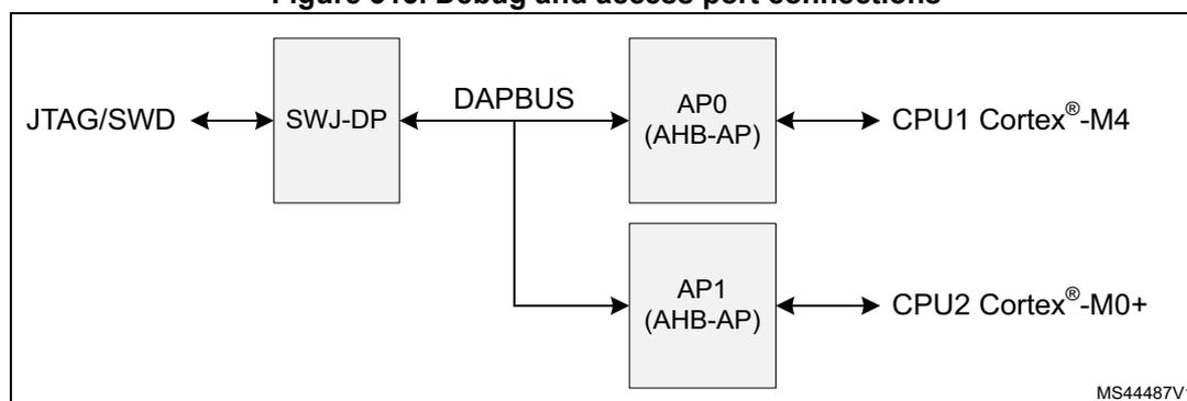
As shown in Figure 315 , there are two access ports (AP) attached to the DP:
- 1. AP0: CPU1 (Cortex ® -M4) access port (AHB-AP): enables access to the debug and trace features integrated in the Cortex ® -M4 processor core via its internal AHB bus.
- 2. AP1: CPU2 (Cortex ® -M0+) access port (AHB-AP): enables access to the debug and trace features integrated in the Cortex ® -M0+ processor core via its internal AHB bus.
Both access ports are of type MEM-AP, the debug and trace component registers are mapped in the address space of the associated debug bus. The AP is seen by the debugger as a set of 32-bit registers organized in banks of four registers each. Some of these registers are used to configure or monitor the AP itself, while others are used to perform a transfer on the bus. The AP registers are listed in Table 213 .
Figure 315. Debug and access port connections
graph LR
    JTAG_SWD[JTAG/SWD] <--> SWJ_DP[SWJ-DP]
    SWJ_DP <--> DAPBUS[DAPBUS]
    DAPBUS --> AP0["AP0 (AHB-AP)"]
    DAPBUS --> AP1["AP1 (AHB-AP)"]
    AP0 <--> CPU1["CPU1 Cortex®-M4"]
    AP1 <--> CPU2["CPU2 Cortex®-M0+"]
The address of the AP registers is composed of
- • Bits [7:4]: content of the SELECT register APBANKSEL field in the DP (see Section 33.4.11 )
- • Bits [3:2]: content of the A(3:2) field of the APACC data register in the JTAG-DP (see Table 212 ) or of the SW-DP Packet Request (see Table 209 ), depending on the debug interface used
- • Bits [1:0]: Always set to 0
The content of the SELECT register APSEL field in the DP defines which MEM-AP is being accessed.
The debugger can access the AP registers as follows:
- 1. Program the SELECT register APSEL field in the DP to choose one of the APs, and the APBANKSEL field to select the register bank to be accessed (see Section 33.4.11 ).
- 2. Program the A(3:2) field in the APACC register, if using JTAG, with the register address within the bank. Program the RnW bit to select a Read or Write. In the case of a write, program the DATA field with the write data. If using SWD, the A(3:2) and RnW fields are part of the Packet Request word sent to the SW-DP with the APnDP bit set (see Table 209 ). The write data is sent in the data phase.
The debugger can access the memory mapped debug component registers through the MEM-AP registers (i.e. using the above AP register access procedure) as follows:
- 1. Program the transaction target address in the TAR register.
- 2. Program the CSW register, if necessary, with the transfer parameters (AddrInc for example).
- 3. Write to or read from the DRW register to initiate a bus transaction at the address held in the TAR register. Alternatively, a read or write to Banked data register BDN triggers an access to address \( TAR[31:4] + n \) (this enables up to four consecutive addresses to be accessed without changing the address in the TAR register).
For more detailed information on the MEM-AP, refer to the Arm ® Debug Interface Architecture Specification [1].
33.5.1 AP control/status word register (AP_CSWR)
Address offset: 0x0
Reset value: 0x2300 0040
| 31 | 30 | 29 | 28 | 27 | 26 | 25 | 24 | 23 | 22 | 21 | 20 | 19 | 18 | 17 | 16 |
|---|---|---|---|---|---|---|---|---|---|---|---|---|---|---|---|
| Res. | SPROT | Res. | PROT[4:0] | SPI STATUS | Res. | Res. | Res. | Res. | Res. | Res. | Res. | ||||
| r | r | r | r | r | r | ||||||||||
| 15 | 14 | 13 | 12 | 11 | 10 | 9 | 8 | 7 | 6 | 5 | 4 | 3 | 2 | 1 | 0 |
| Res. | Res. | Res. | Res. | MODE[3:0] | TRIN PROG | DEVICE EN | ADDRIN[1:0] | Res. | SIZE[2:0] | ||||||
| r | r | r | r | r | r | r | r | r | r | r | |||||
Bit 31 Reserved, must be kept at reset value.
Bit 30 SPROT : Secure transfer request. In the AHB-APs this field sets the protection attribute HPROT[6] of the bus transfer.
0: If SPIDEN is high, secure transfer. If SPIDEN is low, non-secure transfer.
1: Non-secure transfer.
Bit 29 Reserved, must be kept at reset value.
Bits 28:24 PROT[4:0] : Bus transfer protection. In the AHB-APs this field sets the protection attributes HPROT[4:0] of the bus transfer.
- 0bXXXX0: Instruction fetch
- 0bXXXX1: Data access
- 0bXXX0X: User mode
- 0bXXX1X: Privileged mode
- 0bXX0XX: Non-bufferable
- 0bXX1XX: Bufferable
- 0bX0XXX: Non-cacheable
- 0bX1XXX: Cacheable
- 0b0XXXX: Non-exclusive
- 0b1XXXX: Exclusive
Bit 23 SPSTATUS : Status of SPIDEN option bit (read only). This signal determines whether the debugger can access secure memory.
0: Secure AHB transfers are blocked
1: Secure AHB transfers are allowed
Bits 22:12 Reserved, must be kept at reset value.
Bits 11:8 MODE[3:0] : Barrier support enabled. Defines if memory barrier operation is supported.
0x0: Not supported
Bit 7 TRINPROG : Transfer in progress (read only). Indicates if a bus transfer is in progress on the AP.
0x0: No transfer in progress.
0x1: Bus transfer in progress.
Bit 6 DEVICEEN : Device enabled (read only). Defines whether the AP can be accessed.
0x1: AP access enabled.
Bits 5:4 ADDRINC[1:0] : Auto-increment mode. Defines whether TAR address is automatically incremented after a transaction.
0x0: No auto-increment
0x1: Address is incremented by the size in bytes of the transaction (SIZE field).
0x2: Packed transfers enabled. A 32-bit AP access gives rise to 1 x 32-bit, 2 x 16-bit, or 4 x 8-bit bus transactions, corresponding to the programmed transaction size. Data are packed or unpacked accordingly.
0x3: reserved
Bit 3 Reserved, must be kept at reset value.
Bits 2:0 SIZE[2:0] : Size of next memory access transaction
0x0: Byte (8-bit)
0x1: Halfword (16-bit)
0x2: Word (32-bit)
0x3-0x7: reserved
33.5.2 AP transfer address register (AP_TAR)
Address offset: 0x04
Reset value: 0x0000 0000
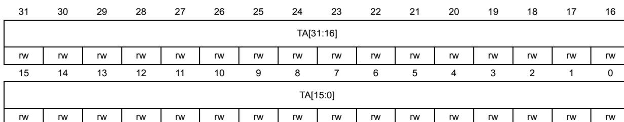
| 31 | 30 | 29 | 28 | 27 | 26 | 25 | 24 | 23 | 22 | 21 | 20 | 19 | 18 | 17 | 16 |
| TA[31:16] | |||||||||||||||
| rw | rw | rw | rw | rw | rw | rw | rw | rw | rw | rw | rw | rw | rw | rw | rw |
| 15 | 14 | 13 | 12 | 11 | 10 | 9 | 8 | 7 | 6 | 5 | 4 | 3 | 2 | 1 | 0 |
| TA[15:0] | |||||||||||||||
| rw | rw | rw | rw | rw | rw | rw | rw | rw | rw | rw | rw | rw | rw | rw | rw |
Bits 31:0 TA[31:0] : Address of current transfer
33.5.3 AP data read/write register (AP_DRWR)
Address offset: 0x0C
Reset value: 0x0000 0000

| 31 | 30 | 29 | 28 | 27 | 26 | 25 | 24 | 23 | 22 | 21 | 20 | 19 | 18 | 17 | 16 |
| TD[31:16] | |||||||||||||||
| rw | rw | rw | rw | rw | rw | rw | rw | rw | rw | rw | rw | rw | rw | rw | rw |
| 15 | 14 | 13 | 12 | 11 | 10 | 9 | 8 | 7 | 6 | 5 | 4 | 3 | 2 | 1 | 0 |
| TD[15:0] | |||||||||||||||
| rw | rw | rw | rw | rw | rw | rw | rw | rw | rw | rw | rw | rw | rw | rw | rw |
Bits 31:0 TD[31:0] : Data of current transfer
33.5.4 AP banked data registers (AP_BD0-3R)
Address offset: 0x10 (DB0R)
Address offset: 0x14 (BD1R)
Address offset: 0x18 (BD2R)
Address offset: 0x1C (BD3R)
Reset value: 0x0000 0000
| 31 | 30 | 29 | 28 | 27 | 26 | 25 | 24 | 23 | 22 | 21 | 20 | 19 | 18 | 17 | 16 |
|---|---|---|---|---|---|---|---|---|---|---|---|---|---|---|---|
| TBD[31:16] | |||||||||||||||
| rw | rw | rw | rw | rw | rw | rw | rw | rw | rw | rw | rw | rw | rw | rw | rw |
| 15 | 14 | 13 | 12 | 11 | 10 | 9 | 8 | 7 | 6 | 5 | 4 | 3 | 2 | 1 | 0 |
| TBD[15:0] | |||||||||||||||
| rw | rw | rw | rw | rw | rw | rw | rw | rw | rw | rw | rw | rw | rw | rw | rw |
Bits 31:0 TBD[31:0] : Banked data of current transfer to address TAR. TA+ AP_BDnR address [3:2] + 0b00. Auto address incrementing is not performed on AP_BD0-3R. Banked transfers are only supported for word transfers.
33.5.5 AP base address register (AP_BASER)
Address offset: 0xF8
Reset value: 0xE00F F003 (AP0), 0xF000 0003 (AP1)
| 31 | 30 | 29 | 28 | 27 | 26 | 25 | 24 | 23 | 22 | 21 | 20 | 19 | 18 | 17 | 16 |
|---|---|---|---|---|---|---|---|---|---|---|---|---|---|---|---|
| BASEADDR[19:4] | |||||||||||||||
| r | r | r | r | r | r | r | r | r | r | r | r | r | r | r | r |
| 15 | 14 | 13 | 12 | 11 | 10 | 9 | 8 | 7 | 6 | 5 | 4 | 3 | 2 | 1 | 0 |
| BASEADDR[3:0] | Res. | Res. | Res. | Res. | Res. | Res. | Res. | Res. | Res. | Res. | FORMAT | ENTRY PRESENT | |||
| r | r | r | r | r | r | ||||||||||
Bits 31:12 BASEADDR[19:0] : Base address (bits 31 to 12) of ROM table for the AP. The twelve LSBs are 0 since the ROM table must be aligned on a 4-Kbyte boundary.
AP0 CPU1 (Cortex®-M4) AHB-AP: 0xE00FF
AP1 CPU2 (Cortex®-M0+) AHB-AP: 0xF0000
Bits 11:2 Reserved, must be kept at reset value.
Bit 1 FORMAT : Base address register format.
1: Arm® debug interface v5
Bit 0 ENTRYPRESENT : Indicates that debug components are present on the access port bus.
1: Debug components are present
33.5.6 AP identification register (AP_IDR)
Address offset: 0xFC
Reset value: 0x2477 0011 (AP0), 0x6477 0001 (AP1)
Read only
| 31 | 30 | 29 | 28 | 27 | 26 | 25 | 24 | 23 | 22 | 21 | 20 | 19 | 18 | 17 | 16 |
|---|---|---|---|---|---|---|---|---|---|---|---|---|---|---|---|
| REVISION[3:0] | JEDECBANK[3:0] | JEDECCODE[6:0] | MEMAP | ||||||||||||
| r | r | r | r | r | r | r | r | r | r | r | r | r | r | r | r |
| 15 | 14 | 13 | 12 | 11 | 10 | 9 | 8 | 7 | 6 | 5 | 4 | 3 | 2 | 1 | 0 |
| Res. | Res. | Res. | Res. | Res. | Res. | Res. | Res. | IDENTITY[7:0] | |||||||
| r | r | r | r | r | r | r | r | ||||||||
0x2: r0p3
0x6: r0p7
Bits 27:24 JEDECBANK[3:0] : JEDEC bank.0x4: Arm ® Bits 23:17 JEDECCODE[6:0] : JEDEC code.0x3B: Arm ® Bit 16 MEMAP : Memory access port.0x1: Standard register map
Bits 15:8 Reserved, must be kept at reset value.
Bits 7:0 IDENTITY[7:0] : Identifies the type of AP.0x11: CPU1 (Cortex ® -M4) AHB-AP (AP0)0x01: CPU2 (Cortex ® -M0+) AHB-AP (AP1)33.5.7 Access port register map and reset values
These registers are not on the CPU memory bus, they are only accessed through SW-DP and JTAG-DP debug interface.
The access port address is 8-bit wide, defined by debug port register DP_SELECTR.APBANKSEL[3:0] field, and by JTAG-DP register DPACC or SW-DP packet request A[3:2] field.
Table 213. Access port register map and reset values
| Offset | Register name | 31 | 30 | 29 | 28 | 27 | 26 | 25 | 24 | 23 | 22 | 21 | 20 | 19 | 18 | 17 | 16 | 15 | 14 | 13 | 12 | 11 | 10 | 9 | 8 | 7 | 6 | 5 | 4 | 3 | 2 | 1 | 0 |
|---|---|---|---|---|---|---|---|---|---|---|---|---|---|---|---|---|---|---|---|---|---|---|---|---|---|---|---|---|---|---|---|---|---|
| 0x00 | AP_CSWR | Res. | SPROT | Res. | PROT[4:0] | SPISTATUS | Res. | Res. | Res. | Res. | Res. | Res. | Res. | Res. | Res. | Res. | MODE[3:0] | TRINPROG [1:0] | ADDRIN [1:0] | Res. | SIZE [2:0] | ||||||||||||
| Reset value | 0 | 0 | 0 | 0 | 1 | 1 | 0 | 0 | 0 | 0 | 0 | 0 | 1 | 0 | 0 | 0 | 0 | 0 | |||||||||||||||
| 0x04 | AP_TAR | TA[0:31] | |||||||||||||||||||||||||||||||
| Reset value | 0 | 0 | 0 | 0 | 0 | 0 | 0 | 0 | 0 | 0 | 0 | 0 | 0 | 0 | 0 | 0 | 0 | 0 | 0 | 0 | 0 | 0 | 0 | 0 | 0 | 0 | 0 | 0 | 0 | 0 | 0 | 0 | |
| 0x0C | AP_DRWR | TD[0:31] | |||||||||||||||||||||||||||||||
| Reset value | 0 | 0 | 0 | 0 | 0 | 0 | 0 | 0 | 0 | 0 | 0 | 0 | 0 | 0 | 0 | 0 | 0 | 0 | 0 | 0 | 0 | 0 | 0 | 0 | 0 | 0 | 0 | 0 | 0 | 0 | 0 | 0 | |
| 0x10 | AP_BD0R | TBD[0:31] | |||||||||||||||||||||||||||||||
| Reset value | 0 | 0 | 0 | 0 | 0 | 0 | 0 | 0 | 0 | 0 | 0 | 0 | 0 | 0 | 0 | 0 | 0 | 0 | 0 | 0 | 0 | 0 | 0 | 0 | 0 | 0 | 0 | 0 | 0 | 0 | 0 | 0 | |
| 0x14 | AP_BD1R | TBD[0:31] | |||||||||||||||||||||||||||||||
| Reset value | 0 | 0 | 0 | 0 | 0 | 0 | 0 | 0 | 0 | 0 | 0 | 0 | 0 | 0 | 0 | 0 | 0 | 0 | 0 | 0 | 0 | 0 | 0 | 0 | 0 | 0 | 0 | 0 | 0 | 0 | 0 | 0 | |
| 0x18 | AP_BD2R | TBD[0:31] | |||||||||||||||||||||||||||||||
| Reset value | 0 | 0 | 0 | 0 | 0 | 0 | 0 | 0 | 0 | 0 | 0 | 0 | 0 | 0 | 0 | 0 | 0 | 0 | 0 | 0 | 0 | 0 | 0 | 0 | 0 | 0 | 0 | 0 | 0 | 0 | 0 | 0 | |
| 0x1C | AP_BD3R | TBD[0:31] | |||||||||||||||||||||||||||||||
| Reset value | 0 | 0 | 0 | 0 | 0 | 0 | 0 | 0 | 0 | 0 | 0 | 0 | 0 | 0 | 0 | 0 | 0 | 0 | 0 | 0 | 0 | 0 | 0 | 0 | 0 | 0 | 0 | 0 | 0 | 0 | 0 | 0 | |
| 0xF8 | AP_BASER | BASEADDR[0:19] | FORMAT | ENTRYPRESENT | |||||||||||||||||||||||||||||
| Reset value (AP0) | 1 | 1 | 1 | 0 | 0 | 0 | 0 | 0 | 0 | 0 | 0 | 0 | 1 | 1 | 1 | 1 | 1 | 1 | 1 | 1 | 0 | 0 | 0 | 0 | 0 | 0 | 0 | 0 | 0 | 0 | 1 | 1 | |
| Reset value (AP1) | 1 | 1 | 1 | 1 | 0 | 0 | 0 | 0 | 0 | 0 | 0 | 0 | 0 | 0 | 0 | 0 | 0 | 0 | 0 | 0 | 0 | 0 | 0 | 0 | 0 | 0 | 0 | 0 | 0 | 0 | 1 | 1 | |
| 0xFC | AP_IDR | REVISION [3:0] | JEDECBANK [3:0] | JEDECCODE[6:0] | MEMAP | Res. | Res. | Res. | Res. | Res. | Res. | Res. | Res. | IDENTITY[7:0] | |||||||||||||||||||
| Reset value (AP0) | 0 | 0 | 1 | 0 | 0 | 1 | 0 | 0 | 0 | 1 | 1 | 1 | 0 | 1 | 1 | 1 | 0 | 0 | 0 | 1 | 0 | 0 | 0 | 1 | |||||||||
| Reset value (AP1) | 0 | 1 | 1 | 0 | 0 | 1 | 0 | 0 | 0 | 1 | 1 | 1 | 0 | 1 | 1 | 1 | 0 | 0 | 0 | 0 | 0 | 0 | 0 | 1 | |||||||||
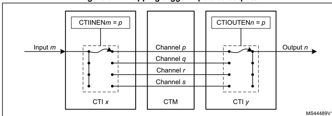
33.6 Cross trigger interface (CTI) and matrix (CTM)
The Cross trigger interfaces (CTIs) and Cross trigger matrix (CTM), taken together, form the CoreSight™ embedded cross trigger (see Figure 316 ).
There are two CTI components, one dedicated to the CPU2 and one dedicated to the CPU1. The CTIs are connected to each other via the CTM. The CTI registers are accessible to the debugger via the corresponding access port and associated AHB.
![Diagram of the Embedded cross trigger architecture. It shows two Cortex-M cores (M0+ and M4) connected to their respective CTIs. The Cortex-M0+ CPU is connected to the Cortex-M0+ CTI via AHB, HALTED, EDBGREQ, and DBGRESTART signals. The Cortex-M4 CPU is connected to the Cortex-M4 CTI via PPB, CMPMATCH0, CMPMATCH1, CMPMATCH2, HALTED, EDBGREQ, and DBGRESTART signals. The DWT is also connected to the Cortex-M4 CTI via CMPMATCH signals. The CTIs are interconnected via CTM channels [3:0].](/RM0473-STM32WB15CC/77b0e869bd427f6bb07c638ac65faa67_img.jpg)
Figure 316. Embedded cross trigger
The diagram illustrates the embedded cross trigger architecture. At the top, a Cortex®-M0+ CPU is connected to a Cortex®-M0+ CTI via an AHB interface. The CPU sends HALTED, EDBGREQ, and DBGRESTART signals to the CTI. The CTI has TRIGIN0, TRIGOUT0, and TRIGOUT7 pins. Below, a Cortex®-M4 CPU is connected to a Cortex®-M4 CTI via a PPB interface. The CPU sends HALTED, EDBGREQ, and DBGRESTART signals to the CTI. The CTI has TRIGIN0, TRIGOUT0, and TRIGOUT7 pins. A DWT (Debug Watchpoint and Trace) component is also connected to the Cortex®-M4 CTI via CMPMATCH0, CMPMATCH1, and CMPMATCH2 signals. The Cortex®-M4 CTI has TRIGIN4, TRIGIN5, TRIGIN6, TRIGIN0, TRIGOUT0, and TRIGOUT7 pins. A vertical line labeled 'CTM channels [3:0]' connects the two CTIs, indicating cross-triggering capabilities.
The CTIs enable events from various sources to trigger debug and/or trace activity. For example, a breakpoint reached in one of the processor cores can stop the other processor, or a transition detected on an external trigger input can start code trace.
Each CTI has up to eight trigger inputs and eight trigger outputs. Any input can be connected to any output, on the same CTI, or on another CTI via the CTM.
The trigger input and output signals for each CTI are listed in tables 214 to 217 .
Table 214. CPU2 CTI inputs
| No. | Source signal | Source component | Comments |
|---|---|---|---|
| 0 | HALTED | CPU2 | CPU2 halted - Indicates CPU2 is in debug mode |
| 1 | - | - | Not used |
| 2 | - | - | Not used |
| 3 | - | - | Not used |
| 4 | - | - | Not used |
| 5 | - | - | Not used |
| 6 | - | - | Not used |
| 7 | - | - | Not used |
Table 215. CPU2 CTI outputs
| No. | Output signal | Destination component | Comments |
|---|---|---|---|
| 0 | EDBGRQ | CPU2 | CPU2 halt request - Puts CPU2 in debug mode |
| 1 | - | - | Not used |
| 2 | - | - | Not used |
| 3 | - | - | Not used |
| 4 | - | - | Not used |
| 5 | - | - | Not used |
| 6 | - | - | Not used |
| 7 | DBGRESTART | CPU2 | CPU2 restart request - CPU2 exits debug mode |
Table 216. CPU1 CTI inputs
| No. | Source signal | Source component | Comments |
|---|---|---|---|
| 0 | HALTED | CPU1 | CPU1 halted - Indicates CPU1 is in debug mode |
| 1 | - | - | Not used |
| 2 | - | - | Not used |
| 3 | - | - | Not used |
| 4 | CMPMATCH0 | CPU1 DWT | DWT comparator 0 match |
| 5 | CMPMATCH1 | CPU1 DWT | DWT comparator 1 match |
| 6 | CMPMATCH2 | CPU1 DWT | DWT comparator 2 match |
| 7 | - | - | Not used |
Table 217. CPU1 CTI outputs
| No. | Source signal | Source component | Comments |
|---|---|---|---|
| 0 | EDBGRQ | CPU1 | CPU1 halt request - Puts CPU1 in debug mode |
| 1 | - | - | Not used |
| 2 | - | - | Not used |
| 3 | - | - | Not used |
| 4 | - | - | Not used |
| 5 | - | - | Not used |
| 6 | - | - | Not used |
| 7 | DBGRESTART | CPU1 | CPU1 restart request - CPU1 exits debug mode |
There are four event channels in the cross trigger matrix, thus enabling up to four, parallel, bidirectional connections between trigger inputs and outputs on different CTIs. To connect input number \( m \) on CTI \( x \) to output number \( n \) on CTI \( y \) , the input must be connected to an event channel \( p \) using the CTIINEN \( m \) register of CTI \( x \) . The same channel \( p \) must be connected to the output using the CTIOUTEN \( n \) register of CTI \( y \) .
Note: This applies even if the input and output belong to the same CTI.
An input can be connected to more than one channel (up to four), so an input can be routed to several outputs. Similarly, an output can be connected to several inputs. It is also possible to connect several inputs/outputs to the same channel.
Figure 317. Mapping trigger inputs to outputs
Example configurations
When either CPU core hits a breakpoint, stop the other core. Restart the two cores synchronously.
To stop both cores when one of them stops the HALTED output of each core must be connected to the EDBGREQ input of the opposite core.
Referring to Table 214 and Table 216 , we see that the HALTED signal from the CPU2 is connected to input 0 of the CPU2 CTI, and the same signal from the CPU1 is connected to the same input on the CPU1 CTI. Hence we program the CTIIEIN0 register on each CTI to connect these inputs to a CTM channel (eg. channel 0).
From Table 215 and Table 217 we see that the EDBGREQ signals to the CPUs are connected to output 0 of the respective CTIs. So we program the CTIOUTEN0 register on each CTI to connect these outputs to the same CTM channel.
To restart both cores simultaneously the debugger must use the APPULSE register in one of the CTIs. This allows the debugger to generate a pulse on any of the four CTM channels. The channel must be connected to the DBGRESTART signal of both cores.
From Table 215 and Table 217 we see that the DBGRESTART signals to the CPUs are connected to output 1 of the respective CTIs. So we program the CTIOUTEN1 register on each CTI, to connect these outputs to an unused CTM channel (e.g. channel 1).
The above configuration is illustrated in Figure 318 .
Figure 318. Cross trigger configuration example
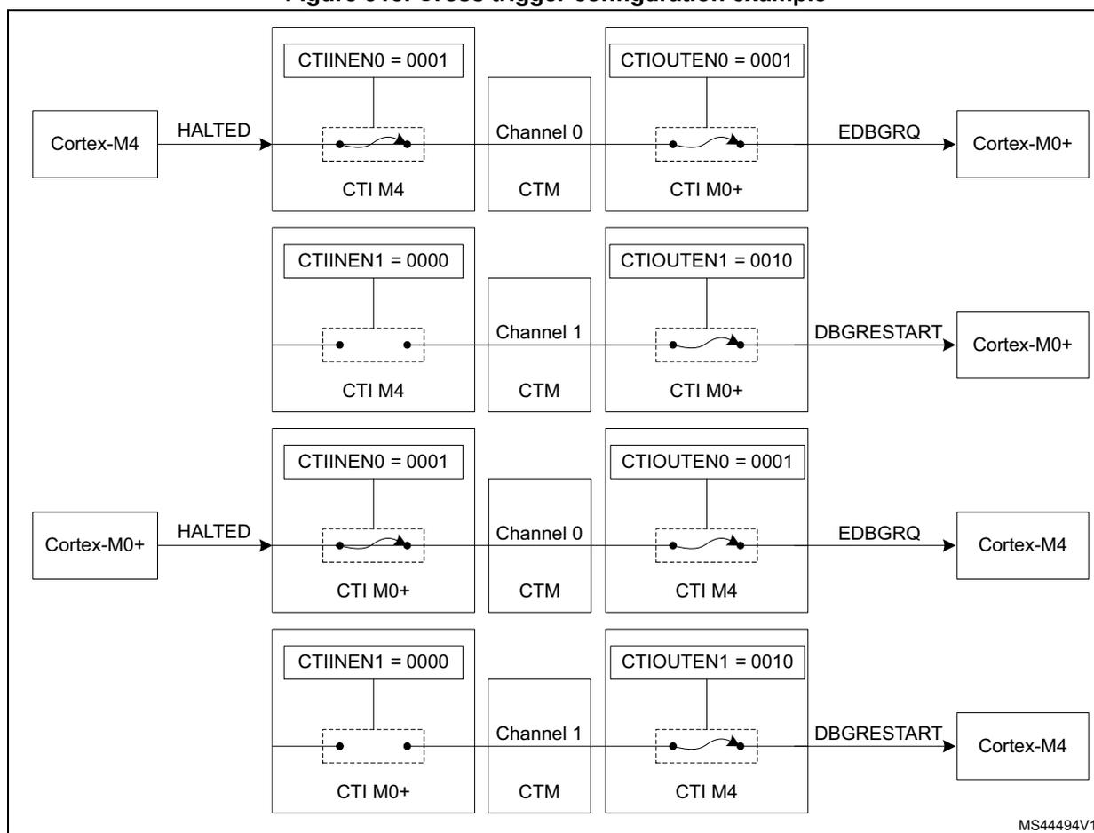
To force the processors to restart simultaneously, use the following procedure:
- 1. Clear the debug request by writing 0x01, then 0x00, to the CTIINTACK register in each CTI.
- 2. Cause a pulse on channel 1 by writing 0x02 to the APPPULSE register in either CTI. This generates a restart request to both processors.
Note that the debugger can also force both cores to stop simultaneously by writing 0x01 to the APPPULSE register in either CTI, which generates a pulse on channel 0.
For more information on the Cross-Trigger Interface CoreSight™ component refer to the Arm® CoreSight™ SoC-400 Technical Reference Manual [2].
33.7 Cross trigger interface registers
The register file base address is 0xE0043000 for CPU1 CTI and 0xF0001000 for CPU2 CTI. CPU1 CTI and CPU2 CTI are accessed via different access ports. The registers are the same for each CTI.
33.7.1 CTI control register (CTI_CONTROLR)
Address offset: 0x000
Reset value: 0x0000 0000
| 31 | 30 | 29 | 28 | 27 | 26 | 25 | 24 | 23 | 22 | 21 | 20 | 19 | 18 | 17 | 16 |
|---|---|---|---|---|---|---|---|---|---|---|---|---|---|---|---|
| Res. | Res. | Res. | Res. | Res. | Res. | Res. | Res. | Res. | Res. | Res. | Res. | Res. | Res. | Res. | Res. |
| 15 | 14 | 13 | 12 | 11 | 10 | 9 | 8 | 7 | 6 | 5 | 4 | 3 | 2 | 1 | 0 |
| Res. | Res. | Res. | Res. | Res. | Res. | Res. | Res. | Res. | Res. | Res. | Res. | Res. | Res. | Res. | GLBEN |
| rw |
Bits 31:1 Reserved, must be kept at reset value.
Bit 0 GLBEN : Global enable.
0: Cross-triggering disabled
1: Cross-triggering enabled
33.7.2 CTI trigger acknowledge register (CTI_INTACKR)
Address offset: 0x010
Reset value: 0x0000 0000
| 31 | 30 | 29 | 28 | 27 | 26 | 25 | 24 | 23 | 22 | 21 | 20 | 19 | 18 | 17 | 16 |
|---|---|---|---|---|---|---|---|---|---|---|---|---|---|---|---|
| Res. | Res. | Res. | Res. | Res. | Res. | Res. | Res. | Res. | Res. | Res. | Res. | Res. | Res. | Res. | Res. |
| 15 | 14 | 13 | 12 | 11 | 10 | 9 | 8 | 7 | 6 | 5 | 4 | 3 | 2 | 1 | 0 |
| Res. | Res. | Res. | Res. | Res. | Res. | Res. | Res. | INTACK[7:0] | |||||||
| rw | rw | rw | rw | rw | rw | rw | rw | ||||||||
Bits 31:8 Reserved, must be kept at reset value.
Bit 7:0 INTACK[7:0] : Trigger acknowledge.
There is one bit of the register for each CTITRIGOUT output. When a 1 is written to a bit in this register, the corresponding CTITRIGOUT output is acknowledged, causing it to be cleared.
33.7.3 CTI application trigger set register (CTI_APPSETR)
Address offset: 0x014
Reset value: 0x0000 0000
| 31 | 30 | 29 | 28 | 27 | 26 | 25 | 24 | 23 | 22 | 21 | 20 | 19 | 18 | 17 | 16 |
|---|---|---|---|---|---|---|---|---|---|---|---|---|---|---|---|
| Res. | Res. | Res. | Res. | Res. | Res. | Res. | Res. | Res. | Res. | Res. | Res. | Res. | Res. | Res. | Res. |
| 15 | 14 | 13 | 12 | 11 | 10 | 9 | 8 | 7 | 6 | 5 | 4 | 3 | 2 | 1 | 0 |
| Res. | Res. | Res. | Res. | Res. | Res. | Res. | Res. | Res. | Res. | Res. | Res. | APPSET[3:0] | |||
| rw | |||||||||||||||
Bits 31:4 Reserved, must be kept at reset value.
Bit 3:0 APPSET[3:0] : Set channel event.
Read:
- 0bXXX0: Channel 0 event inactive
- 0bXXX1: Channel 0 event active
- 0bXX0X: Channel 1 event inactive
- 0bXX1X: Channel 1 event active
- 0bX0XX: Channel 2 event inactive
- 0bX1XX: Channel 2 event active
- 0b0XXX: Channel 3 event inactive
- 0b1XXX: Channel 3 event active
Write:
- 0bXXX0: No effect
- 0bXXX1: Set event on Channel 0
- 0bXX0X: No effect
- 0bXX1X: Set event on Channel 1
- 0bX0XX: No effect
- 0bX1XX: Set event on Channel 2
- 0b0XXX: No effect
- 0b1XXX: Set event on Channel 3
33.7.4 CTI application trigger clear register (CTI_APPCLEAR)
Address offset: 0x018
Reset value: 0x0000 0000
| 31 | 30 | 29 | 28 | 27 | 26 | 25 | 24 | 23 | 22 | 21 | 20 | 19 | 18 | 17 | 16 |
|---|---|---|---|---|---|---|---|---|---|---|---|---|---|---|---|
| Res. | Res. | Res. | Res. | Res. | Res. | Res. | Res. | Res. | Res. | Res. | Res. | Res. | Res. | Res. | Res. |
| 15 | 14 | 13 | 12 | 11 | 10 | 9 | 8 | 7 | 6 | 5 | 4 | 3 | 2 | 1 | 0 |
| Res. | Res. | Res. | Res. | Res. | Res. | Res. | Res. | Res. | Res. | Res. | Res. | APPCLEAR[3:0] | |||
| w | |||||||||||||||
Bits 31:4 Reserved, must be kept at reset value.
Bit 3:0 APPCLEAR[3:0] : Clear channel event.
0b0000: No effect
0bXXX1: Clear event on Channel 0
0bXX1X: Clear event on Channel 1
0bX1XX: Clear event on Channel 2
0b1XXX: Clear event on Channel 3
33.7.5 CTI application pulse register (CTI_APPPULSER)
Address offset: 0x01C
Reset value: 0x0000 0000
| 31 | 30 | 29 | 28 | 27 | 26 | 25 | 24 | 23 | 22 | 21 | 20 | 19 | 18 | 17 | 16 |
|---|---|---|---|---|---|---|---|---|---|---|---|---|---|---|---|
| Res. | Res. | Res. | Res. | Res. | Res. | Res. | Res. | Res. | Res. | Res. | Res. | Res. | Res. | Res. | Res. |
| 15 | 14 | 13 | 12 | 11 | 10 | 9 | 8 | 7 | 6 | 5 | 4 | 3 | 2 | 1 | 0 |
| Res. | Res. | Res. | Res. | Res. | Res. | Res. | Res. | Res. | Res. | Res. | Res. | APPPULSE[3:0] | |||
| w | |||||||||||||||
Bits 31:4 Reserved, must be kept at reset value.
Bit 3:0 APPPULSE[3:0] : Pulse channel event. This register clears itself immediately.
0b0000: No effect
0bXXX1: Generate pulse on Channel 0
0bXX1X: Generate pulse on Channel 1
0bX1XX: Generate pulse on Channel 2
0b1XXX: Generate pulse on Channel 3
33.7.6 CTI trigger In x enable register (CTI_INENRx)
Address offset: 0x020 + 4 * x, where x = 0 to 7
Reset value: 0x0000 0000
| 31 | 30 | 29 | 28 | 27 | 26 | 25 | 24 | 23 | 22 | 21 | 20 | 19 | 18 | 17 | 16 |
|---|---|---|---|---|---|---|---|---|---|---|---|---|---|---|---|
| Res. | Res. | Res. | Res. | Res. | Res. | Res. | Res. | Res. | Res. | Res. | Res. | Res. | Res. | Res. | Res. |
| 15 | 14 | 13 | 12 | 11 | 10 | 9 | 8 | 7 | 6 | 5 | 4 | 3 | 2 | 1 | 0 |
| Res. | Res. | Res. | Res. | Res. | Res. | Res. | Res. | Res. | Res. | Res. | Res. | TRIGINEN[3:0] | |||
| rw | |||||||||||||||
Bits 31:4 Reserved, must be kept at reset value.
Bit 3:0 TRIGINEN[3:0] : Enables or disables a cross trigger event on each of the four channels when CTITRIGINx is activated (x = 0 to 7).
0b0000: Trigger does not generate events on Channels
0bXXX1: Trigger n generates events on Channel 0
0bXX1X: Trigger n generates events on Channel 1
0bX1XX: Trigger n generates events on Channel 2
0b1XXX: Trigger n generates events on Channel 3
33.7.7 CTI trigger out x enable register (CTI_OUTENRx)
Address offset: 0x0A0 + 4 * x, where x = 0 to 7
Reset value: 0x0000 0000
| 31 | 30 | 29 | 28 | 27 | 26 | 25 | 24 | 23 | 22 | 21 | 20 | 19 | 18 | 17 | 16 |
|---|---|---|---|---|---|---|---|---|---|---|---|---|---|---|---|
| Res. | Res. | Res. | Res. | Res. | Res. | Res. | Res. | Res. | Res. | Res. | Res. | Res. | Res. | Res. | Res. |
| 15 | 14 | 13 | 12 | 11 | 10 | 9 | 8 | 7 | 6 | 5 | 4 | 3 | 2 | 1 | 0 |
| Res. | Res. | Res. | Res. | Res. | Res. | Res. | Res. | Res. | Res. | Res. | Res. | TRIGOUTEN[3:0] | |||
| rw | rw | rw | rw | ||||||||||||
Bits 31:4 Reserved, must be kept at reset value.
Bit 3:0 TRIGOUTEN[3:0] : For each channel, defines whether an event on that channel generates a trigger on CTITRIGOUTx (x = 0 to 7).
0b0000: Channel events do not generate triggers on Trigger outputs
0bXXX1: Channel 0 events generate triggers on Trigger output n
0bXX1X: Channel 1 events generate triggers on Trigger output n
0bX1XX: Channel 2 events generate triggers on Trigger output n
0b1XXX: Channel 3 events generate triggers on Trigger output n
33.7.8 CTI trigger in status register (CTI_TRGISTSR)
Address offset: 0x130
Reset value: 0x0000 0000
| 31 | 30 | 29 | 28 | 27 | 26 | 25 | 24 | 23 | 22 | 21 | 20 | 19 | 18 | 17 | 16 |
|---|---|---|---|---|---|---|---|---|---|---|---|---|---|---|---|
| Res. | Res. | Res. | Res. | Res. | Res. | Res. | Res. | Res. | Res. | Res. | Res. | Res. | Res. | Res. | Res. |
| 15 | 14 | 13 | 12 | 11 | 10 | 9 | 8 | 7 | 6 | 5 | 4 | 3 | 2 | 1 | 0 |
| Res. | Res. | Res. | Res. | Res. | Res. | Res. | Res. | TRIGINSTATUS[7:0] | |||||||
| r | r | r | r | r | r | r | r | ||||||||
Bits 31:8 Reserved, must be kept at reset value.
Bit 7:0 TRIGINSTATUS[7:0] : Trigger input status.
There is one bit of the register for each CTITRIGIN input. When a bit is set to 1 it indicates that the corresponding trigger input is active. When it is set to 0, the corresponding trigger input is inactive.
33.7.9 CTI trigger out status register (CTI_TRGOSTSR)
Address offset: 0x134
Reset value: 0x0000 0000
| 31 | 30 | 29 | 28 | 27 | 26 | 25 | 24 | 23 | 22 | 21 | 20 | 19 | 18 | 17 | 16 |
|---|---|---|---|---|---|---|---|---|---|---|---|---|---|---|---|
| Res. | Res. | Res. | Res. | Res. | Res. | Res. | Res. | Res. | Res. | Res. | Res. | Res. | Res. | Res. | Res. |
| 15 | 14 | 13 | 12 | 11 | 10 | 9 | 8 | 7 | 6 | 5 | 4 | 3 | 2 | 1 | 0 |
| Res. | Res. | Res. | Res. | Res. | Res. | Res. | Res. | TRIGOUTSTATUS[7:0] | |||||||
| r | r | r | r | r | r | r | r | ||||||||
Bits 31:8 Reserved, must be kept at reset value.
Bit 7:0 TRIGOUTSTATUS[7:0] : Trigger output status.
There is one bit of the register for each CTITRIGOUT output. When a bit is set to 1 it indicates that the corresponding trigger output is active. When it is set to 0, the corresponding trigger output is inactive.
33.7.10 CTI channel in status register (CTI_CHINSTSR)
Address offset: 0x138
Reset value: 0x0000 0000
| 31 | 30 | 29 | 28 | 27 | 26 | 25 | 24 | 23 | 22 | 21 | 20 | 19 | 18 | 17 | 16 |
|---|---|---|---|---|---|---|---|---|---|---|---|---|---|---|---|
| Res. | Res. | Res. | Res. | Res. | Res. | Res. | Res. | Res. | Res. | Res. | Res. | Res. | Res. | Res. | Res. |
| 15 | 14 | 13 | 12 | 11 | 10 | 9 | 8 | 7 | 6 | 5 | 4 | 3 | 2 | 1 | 0 |
| Res. | Res. | Res. | Res. | Res. | Res. | Res. | Res. | Res. | Res. | Res. | Res. | CHINSTATUS[3:0] | |||
| r | r | r | r | ||||||||||||
Bits 31:4 Reserved, must be kept at reset value.
Bit 3:0 CHINSTATUS[3:0] : Channel input status.
There is one bit of the register for each channel input. When a bit is set to 1 it indicates that the corresponding channel input is active. When it is set to 0, the corresponding channel input is inactive.
33.7.11 CTI channel out status register (CTI_CHOUTSTSR)
Address offset: 0x13C
Reset value: 0x0000 0000
| 31 | 30 | 29 | 28 | 27 | 26 | 25 | 24 | 23 | 22 | 21 | 20 | 19 | 18 | 17 | 16 |
|---|---|---|---|---|---|---|---|---|---|---|---|---|---|---|---|
| Res. | Res. | Res. | Res. | Res. | Res. | Res. | Res. | Res. | Res. | Res. | Res. | Res. | Res. | Res. | Res. |
| 15 | 14 | 13 | 12 | 11 | 10 | 9 | 8 | 7 | 6 | 5 | 4 | 3 | 2 | 1 | 0 |
| Res. | Res. | Res. | Res. | Res. | Res. | Res. | Res. | Res. | Res. | Res. | Res. | CHOUTSTATUS[3:0] | |||
| r | r | r | r | ||||||||||||
Bits 31:4 Reserved, must be kept at reset value.
Bit 3:0 CHOUTSTATUS[3:0] : Channel output status.
There is one bit of the register for each channel output. When a bit is set to 1 it indicates that the corresponding channel output is active. When it is set to 0, the corresponding channel output is inactive.
33.7.12 CTI channel gate register (CTI_GATER)
Address offset: 0x140
Reset value: 0x0000 000F
| 31 | 30 | 29 | 28 | 27 | 26 | 25 | 24 | 23 | 22 | 21 | 20 | 19 | 18 | 17 | 16 |
|---|---|---|---|---|---|---|---|---|---|---|---|---|---|---|---|
| Res. | Res. | Res. | Res. | Res. | Res. | Res. | Res. | Res. | Res. | Res. | Res. | Res. | Res. | Res. | Res. |
| 15 | 14 | 13 | 12 | 11 | 10 | 9 | 8 | 7 | 6 | 5 | 4 | 3 | 2 | 1 | 0 |
| Res. | Res. | Res. | Res. | Res. | Res. | Res. | Res. | Res. | Res. | Res. | Res. | GATEEN[3:0] | |||
| rw | rw | rw | rw | ||||||||||||
Bits 31:4 Reserved, must be kept at reset value.
Bit 3:0 GATEEN[3:0] : Channel output enable. For each channel, defines whether an event on that channel can propagate over the CTM to other CTIs.
- 0b0000: Channels events do not propagate
- 0bXXX1: Channel 0 events propagate
- 0bXX1X: Channel 1 events propagate
- 0bX1XX: Channel 2 events propagate
- 0b1XXX: Channel 3 events propagate
33.7.13 CTI claim tag set register (CTI_CLAIMSETR)
Address offset: 0xFA0
Reset value: 0x0000 000F
| 31 | 30 | 29 | 28 | 27 | 26 | 25 | 24 | 23 | 22 | 21 | 20 | 19 | 18 | 17 | 16 |
|---|---|---|---|---|---|---|---|---|---|---|---|---|---|---|---|
| Res. | Res. | Res. | Res. | Res. | Res. | Res. | Res. | Res. | Res. | Res. | Res. | Res. | Res. | Res. | Res. |
| 15 | 14 | 13 | 12 | 11 | 10 | 9 | 8 | 7 | 6 | 5 | 4 | 3 | 2 | 1 | 0 |
| Res. | Res. | Res. | Res. | Res. | Res. | Res. | Res. | Res. | Res. | Res. | Res. | CLAIMSET[3:0] | |||
| rw | rw | rw | rw | ||||||||||||
Bits 31:4 Reserved, must be kept at reset value.
Bits 3:0 CLAIMSET[3:0] : Set claim tag bits
Write:
0000: No effect
xxx1: Set bit 0
xx1x: Set bit 1
x1xx: Set bit 2
1xxx: Set bit 3
Read:
0xF: Indicates there are four bits in claim tag
33.7.14 CTI claim tag clear register (CTI_CLAIMCLR)
Address offset: 0xFA4
Reset value: 0x0000 0000
| 31 | 30 | 29 | 28 | 27 | 26 | 25 | 24 | 23 | 22 | 21 | 20 | 19 | 18 | 17 | 16 |
|---|---|---|---|---|---|---|---|---|---|---|---|---|---|---|---|
| Res. | Res. | Res. | Res. | Res. | Res. | Res. | Res. | Res. | Res. | Res. | Res. | Res. | Res. | Res. | Res. |
| 15 | 14 | 13 | 12 | 11 | 10 | 9 | 8 | 7 | 6 | 5 | 4 | 3 | 2 | 1 | 0 |
| Res. | Res. | Res. | Res. | Res. | Res. | Res. | Res. | Res. | Res. | Res. | Res. | CLAIMCLR[3:0] | |||
| rw | rw | rw | rw | ||||||||||||
Bits 31:4 Reserved, must be kept at reset value.
Bits 3:0 CLAIMCLR[3:0] : Reset claim tag bits
Write:
0000: No effect
xxx1: Clear bit 0
xx1x: Clear bit 1
x1xx: Clear bit 2
1xxx: Clear bit 3
Read: Returns current value of claim tag
33.7.15 CTI lock access register (CTI_LAR)
Address offset: 0xFB0
Reset value: N/A
| 31 | 30 | 29 | 28 | 27 | 26 | 25 | 24 | 23 | 22 | 21 | 20 | 19 | 18 | 17 | 16 |
|---|---|---|---|---|---|---|---|---|---|---|---|---|---|---|---|
| ACCESS_W[31:16] | |||||||||||||||
| w | w | w | w | w | w | w | w | w | w | w | w | w | w | w | w |
| 15 | 14 | 13 | 12 | 11 | 10 | 9 | 8 | 7 | 6 | 5 | 4 | 3 | 2 | 1 | 0 |
| ACCESS_W[15:0] | |||||||||||||||
| w | w | w | w | w | w | w | w | w | w | w | w | w | w | w | w |
Bits 31:0
ACCESS_W[31:0]
: Enables write access to some CTI registers by processor cores (debuggers do not need to unlock the component)
0xC5AC CE55: Write access enabled
Other values: Write access disabled
33.7.16 CTI lock status register (CTI_LSR)
Address offset: 0xFB4
Reset value: 0x0000 0003
| 31 | 30 | 29 | 28 | 27 | 26 | 25 | 24 | 23 | 22 | 21 | 20 | 19 | 18 | 17 | 16 |
|---|---|---|---|---|---|---|---|---|---|---|---|---|---|---|---|
| Res. | Res. | Res. | Res. | Res. | Res. | Res. | Res. | Res. | Res. | Res. | Res. | Res. | Res. | Res. | Res. |
| 15 | 14 | 13 | 12 | 11 | 10 | 9 | 8 | 7 | 6 | 5 | 4 | 3 | 2 | 1 | 0 |
| Res. | Res. | Res. | Res. | Res. | Res. | Res. | Res. | Res. | Res. | Res. | Res. | Res. | LOCK TYPE | LOCK GRANT | LOCK EXIST |
| r | r | r |
Bits 31:3 Reserved, must be kept at reset value.
Bit 2
LOCKTYPE
: Indicates the size of the CTI_LAR register
0: 32-bit
Bit 1
LOCKGRANT
: Current status of lock. This bit always reads as zero by an external debugger.
0: Write access is permitted
1: Write access is blocked. Only reads are permitted.
Bit 0
LOCKEXIST
: Indicates whether a lock control mechanism exists. This bit always reads as zero by an external debugger.
0: No lock control mechanism exists.
1: Lock control mechanism is implemented
33.7.17 CTI authentication status register (CTI_AUTHSTATR)
Address offset: 0xFB8
Reset value: 0x0000 000A
| 31 | 30 | 29 | 28 | 27 | 26 | 25 | 24 | 23 | 22 | 21 | 20 | 19 | 18 | 17 | 16 |
|---|---|---|---|---|---|---|---|---|---|---|---|---|---|---|---|
| Res. | Res. | Res. | Res. | Res. | Res. | Res. | Res. | Res. | Res. | Res. | Res. | Res. | Res. | Res. | Res. |
| 15 | 14 | 13 | 12 | 11 | 10 | 9 | 8 | 7 | 6 | 5 | 4 | 3 | 2 | 1 | 0 |
| Res. | Res. | Res. | Res. | Res. | Res. | Res. | Res. | SNID[1:0] | SID[1:0] | NSNID[1:0] | NSID[1:0] | ||||
| r | r | r | r | r | r | r | r |
Bits 31:8 Reserved, must be kept at reset value.
Bits 7:6
SNID[1:0]
: Security level for secure non-invasive debug
0x0: Not implemented
Bits 5:4 SID[1:0] : Security level for secure invasive debug
0x0: Not implemented
Bits 3:2 NSNID[1:0] : Security level for non-secure non-invasive debug
0x2: Disabled
0x3: Enabled
Bits 1:0 NSID[1:0] : Security level for non-secure invasive debug
0x2: Disabled
0x3: Enabled
33.7.18 CTI device configuration register (CTI_DEVIDR)
Address offset: 0xFC8
Reset value: 0x0004 0800
| 31 | 30 | 29 | 28 | 27 | 26 | 25 | 24 | 23 | 22 | 21 | 20 | 19 | 18 | 17 | 16 |
|---|---|---|---|---|---|---|---|---|---|---|---|---|---|---|---|
| Res. | Res. | Res. | Res. | Res. | Res. | Res. | Res. | Res. | Res. | Res. | Res. | NUMCH[3:0] | |||
| r | r | r | r | ||||||||||||
| 15 | 14 | 13 | 12 | 11 | 10 | 9 | 8 | 7 | 6 | 5 | 4 | 3 | 2 | 1 | 0 |
| NUMTRIG[7:0] | Res. | Res. | Res. | EXTMUXNUM[4:0] | |||||||||||
| r | r | r | r | r | r | r | r | r | r | r | r | r | |||
Bits 31:20 Reserved, must be kept at reset value.
Bits 19:16 NUMCH[3:0] : Number of ECT channels available
0x4: 4 channels
Bits 15:8 NUMTRIG[7:0] : Number of ECT triggers available
0x8: 8 trigger inputs and 8 trigger outputs
Bits 7:5 Reserved, must be kept at reset value.
Bits 4:0 EXTMUXNUM[4:0] : Number of trigger input/output multiplexers
0x0: None
33.7.19 CTI device type identifier register (CTI_DEVTYPE)
Address offset: 0xFCC
Reset value: 0x0000 0014
| 31 | 30 | 29 | 28 | 27 | 26 | 25 | 24 | 23 | 22 | 21 | 20 | 19 | 18 | 17 | 16 |
|---|---|---|---|---|---|---|---|---|---|---|---|---|---|---|---|
| Res. | Res. | Res. | Res. | Res. | Res. | Res. | Res. | Res. | Res. | Res. | Res. | Res. | Res. | Res. | Res. |
| 15 | 14 | 13 | 12 | 11 | 10 | 9 | 8 | 7 | 6 | 5 | 4 | 3 | 2 | 1 | 0 |
| Res. | Res. | Res. | Res. | Res. | Res. | Res. | Res. | SUBTYPE[3:0] | MAJORTYPE[3:0] | ||||||
| r | r | r | r | r | r | r | r | ||||||||
Bits 31:8 Reserved, must be kept at reset value.
Bits 7:4 SUBTYPE[3:0] : Sub-classification
0x1: Indicates that this component is a cross-triggering component.
Bits 3:0 MAJORTYPE[3:0] : Major classification
0x4: Indicates that this component allows a debugger to control other components in a CoreSight™ SoC-400 system.
33.7.20 CTI CoreSight peripheral identity register 4 (CTI_PIDR4)
Address offset: 0xFD0
Reset value: 0x0000 0004
| 31 | 30 | 29 | 28 | 27 | 26 | 25 | 24 | 23 | 22 | 21 | 20 | 19 | 18 | 17 | 16 |
|---|---|---|---|---|---|---|---|---|---|---|---|---|---|---|---|
| Res. | Res. | Res. | Res. | Res. | Res. | Res. | Res. | Res. | Res. | Res. | Res. | Res. | Res. | Res. | Res. |
| 15 | 14 | 13 | 12 | 11 | 10 | 9 | 8 | 7 | 6 | 5 | 4 | 3 | 2 | 1 | 0 |
| Res. | Res. | Res. | Res. | Res. | Res. | Res. | Res. | 4KCOUNT[3:0] | JEP106CON[3:0] | ||||||
| r | r | r | r | r | r | r | r | ||||||||
Bits 31:8 Reserved, must be kept at reset value.
Bits 7:4 4KCOUNT[3:0] : register file size
0x0: Register file occupies a single 4 KB region
Bits 3:0 JEP106CON[3:0] : JEP106 continuation code
0x4: Arm® JEDEC code
33.7.21 CTI CoreSight peripheral identity register 0 (CTI_PIDR0)
Address offset: 0xFE0
Reset value: 0x0000 0006
| 31 | 30 | 29 | 28 | 27 | 26 | 25 | 24 | 23 | 22 | 21 | 20 | 19 | 18 | 17 | 16 |
|---|---|---|---|---|---|---|---|---|---|---|---|---|---|---|---|
| Res. | Res. | Res. | Res. | Res. | Res. | Res. | Res. | Res. | Res. | Res. | Res. | Res. | Res. | Res. | Res. |
| 15 | 14 | 13 | 12 | 11 | 10 | 9 | 8 | 7 | 6 | 5 | 4 | 3 | 2 | 1 | 0 |
| Res. | Res. | Res. | Res. | Res. | Res. | Res. | Res. | PARTNUM[7:0] | |||||||
| r | r | r | r | r | r | r | r | ||||||||
Bits 31:8 Reserved, must be kept at reset value.
Bits 7:0 PARTNUM[7:0] : Part number bits [7:0]
0x06: CTI part number
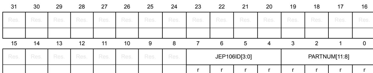
33.7.22 CTI CoreSight peripheral identity register 1 (CTI_PIDR1)
Address offset: 0xFE4
Reset value: 0x0000 00B9
| 31 | 30 | 29 | 28 | 27 | 26 | 25 | 24 | 23 | 22 | 21 | 20 | 19 | 18 | 17 | 16 |
|---|---|---|---|---|---|---|---|---|---|---|---|---|---|---|---|
| Res. | Res. | Res. | Res. | Res. | Res. | Res. | Res. | Res. | Res. | Res. | Res. | Res. | Res. | Res. | Res. |
| 15 | 14 | 13 | 12 | 11 | 10 | 9 | 8 | 7 | 6 | 5 | 4 | 3 | 2 | 1 | 0 |
|---|---|---|---|---|---|---|---|---|---|---|---|---|---|---|---|
| Res. | Res. | Res. | Res. | Res. | Res. | Res. | Res. | JEP106ID[3:0] | PARTNUM[11:8] | ||||||
| r | r | r | r | r | r | r | r | ||||||||
Bit 31:8 Reserved, must be kept at reset value.
Bits 7:4 JEP106ID[3:0] : JEP106 identity code bits [3:0]
0xB: Arm® JEDEC code
Bits 3:0 PARTNUM[11:8] : Part number bits [11:8]
0x9: CTI part number
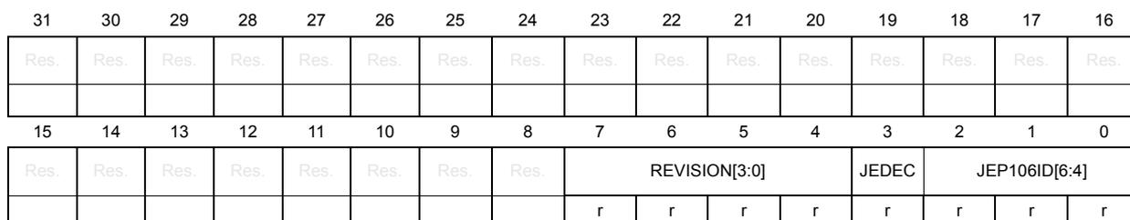
33.7.23 CTI CoreSight peripheral identity register 2 (CTI_PIDR2)
Address offset: 0xFE8
Reset value: 0x0000 004B
| 31 | 30 | 29 | 28 | 27 | 26 | 25 | 24 | 23 | 22 | 21 | 20 | 19 | 18 | 17 | 16 |
|---|---|---|---|---|---|---|---|---|---|---|---|---|---|---|---|
| Res. | Res. | Res. | Res. | Res. | Res. | Res. | Res. | Res. | Res. | Res. | Res. | Res. | Res. | Res. | Res. |
| 15 | 14 | 13 | 12 | 11 | 10 | 9 | 8 | 7 | 6 | 5 | 4 | 3 | 2 | 1 | 0 |
|---|---|---|---|---|---|---|---|---|---|---|---|---|---|---|---|
| Res. | Res. | Res. | Res. | Res. | Res. | Res. | Res. | REVISION[3:0] | JEDEC | JEP106ID[6:4] | |||||
| r | r | r | r | r | r | r | r | ||||||||
Bit 31:8 Reserved, must be kept at reset value.
Bits 7:4 REVISION[3:0] : Component revision number
0x4: r0p5
Bit 3 JEDEC : JEDEC assigned value
0x1: Designer ID specified by JEDEC
Bits 2:0 JEP106ID[6:4] : JEP106 identity code bits [6:4]
0x3: Arm® JEDEC code
33.7.24 CTI CoreSight peripheral identity register 3 (CTI_PIDR3)
Address offset: 0xFEC
Reset value: 0x0000 0000
| 31 | 30 | 29 | 28 | 27 | 26 | 25 | 24 | 23 | 22 | 21 | 20 | 19 | 18 | 17 | 16 |
|---|---|---|---|---|---|---|---|---|---|---|---|---|---|---|---|
| Res. | Res. | Res. | Res. | Res. | Res. | Res. | Res. | Res. | Res. | Res. | Res. | Res. | Res. | Res. | Res. |
| 15 | 14 | 13 | 12 | 11 | 10 | 9 | 8 | 7 | 6 | 5 | 4 | 3 | 2 | 1 | 0 |
| Res. | Res. | Res. | Res. | Res. | Res. | Res. | Res. | REVAND[3:0] | CMOD[3:0] | ||||||
| r | r | r | r | r | r | r | r | ||||||||
Bit 31:8 Reserved, must be kept at reset value.
Bits 7:4 REVAND[3:0] : metal fix version
0x0: No metal fix
Bits 3:0 CMOD[3:0] : Customer modified
0x0: No customer modifications
33.7.25 CTI CoreSight component identity register 0 (CTI_CIDR0)
Address offset: 0xFF0
Reset value: 0x0000 000D
| 31 | 30 | 29 | 28 | 27 | 26 | 25 | 24 | 23 | 22 | 21 | 20 | 19 | 18 | 17 | 16 |
|---|---|---|---|---|---|---|---|---|---|---|---|---|---|---|---|
| Res. | Res. | Res. | Res. | Res. | Res. | Res. | Res. | Res. | Res. | Res. | Res. | Res. | Res. | Res. | Res. |
| 15 | 14 | 13 | 12 | 11 | 10 | 9 | 8 | 7 | 6 | 5 | 4 | 3 | 2 | 1 | 0 |
| Res. | Res. | Res. | Res. | Res. | Res. | Res. | Res. | PREAMBLE[7:0] | |||||||
| r | r | r | r | r | r | r | r | ||||||||
Bits 31:8 Reserved, must be kept at reset value.
Bits 7:0 PREAMBLE[7:0] : Component ID bits [7:0]
0x0D: Common ID value
33.7.26 CTI CoreSight peripheral identity register 1 (CTI_CIDR1)
Address offset: 0xFF4
Reset value: 0x0000 0090
| 31 | 30 | 29 | 28 | 27 | 26 | 25 | 24 | 23 | 22 | 21 | 20 | 19 | 18 | 17 | 16 |
|---|---|---|---|---|---|---|---|---|---|---|---|---|---|---|---|
| Res. | Res. | Res. | Res. | Res. | Res. | Res. | Res. | Res. | Res. | Res. | Res. | Res. | Res. | Res. | Res. |
| 15 | 14 | 13 | 12 | 11 | 10 | 9 | 8 | 7 | 6 | 5 | 4 | 3 | 2 | 1 | 0 |
| Res. | Res. | Res. | Res. | Res. | Res. | Res. | Res. | CLASS[3:0] | PREAMBLE[11:8] | ||||||
| r | r | r | r | r | r | r | r | ||||||||
Bit 31:8 Reserved, must be kept at reset value.
Bits 7:4
CLASS[3:0]
: Component ID bits [15:12] - component class
0x9: CoreSight™ component
Bits 3:0
PREAMBLE[11:8]
: Component ID bits [11:8]
0x0: Common ID value
33.7.27 CTI CoreSight component identity register 2 (CTI_CIDR2)
Address offset: 0xFF8
Reset value: 0x0000 0005
| 31 | 30 | 29 | 28 | 27 | 26 | 25 | 24 | 23 | 22 | 21 | 20 | 19 | 18 | 17 | 16 |
|---|---|---|---|---|---|---|---|---|---|---|---|---|---|---|---|
| Res. | Res. | Res. | Res. | Res. | Res. | Res. | Res. | Res. | Res. | Res. | Res. | Res. | Res. | Res. | Res. |
| 15 | 14 | 13 | 12 | 11 | 10 | 9 | 8 | 7 | 6 | 5 | 4 | 3 | 2 | 1 | 0 |
|---|---|---|---|---|---|---|---|---|---|---|---|---|---|---|---|
| Res. | Res. | Res. | Res. | Res. | Res. | Res. | Res. | PREAMBLE[19:12] | |||||||
| r | r | r | r | r | r | r | r | ||||||||
Bits 31:8 Reserved, must be kept at reset value.
Bits 7:0
PREAMBLE[19:12]
: Component ID bits [23:16]
0x05: Common ID value
33.7.28 CTI CoreSight component identity register 3 (CTI_CIDR3)
Address offset: 0xFFC
Reset value: 0x0000 00B1
| 31 | 30 | 29 | 28 | 27 | 26 | 25 | 24 | 23 | 22 | 21 | 20 | 19 | 18 | 17 | 16 |
|---|---|---|---|---|---|---|---|---|---|---|---|---|---|---|---|
| Res. | Res. | Res. | Res. | Res. | Res. | Res. | Res. | Res. | Res. | Res. | Res. | Res. | Res. | Res. | Res. |
| 15 | 14 | 13 | 12 | 11 | 10 | 9 | 8 | 7 | 6 | 5 | 4 | 3 | 2 | 1 | 0 |
|---|---|---|---|---|---|---|---|---|---|---|---|---|---|---|---|
| Res. | Res. | Res. | Res. | Res. | Res. | Res. | Res. | PREAMBLE[27:20] | |||||||
| r | r | r | r | r | r | r | r | ||||||||
Bits 31:8 Reserved, must be kept at reset value.
Bits 7:0
PREAMBLE[27:20]
: Component ID bits [31:24]
0xB1: Common ID value
33.7.29 CTI register map and reset values
Table 218. CTI register map and reset values
| Offset | Register name | 31 | 30 | 29 | 28 | 27 | 26 | 25 | 24 | 23 | 22 | 21 | 20 | 19 | 18 | 17 | 16 | 15 | 14 | 13 | 12 | 11 | 10 | 9 | 8 | 7 | 6 | 5 | 4 | 3 | 2 | 1 | 0 |
|---|---|---|---|---|---|---|---|---|---|---|---|---|---|---|---|---|---|---|---|---|---|---|---|---|---|---|---|---|---|---|---|---|---|
| 0x000 | CTI_CONTROLR | Res. | Res. | Res. | Res. | Res. | Res. | Res. | Res. | Res. | Res. | Res. | Res. | Res. | Res. | Res. | Res. | Res. | Res. | Res. | Res. | Res. | Res. | Res. | Res. | Res. | Res. | Res. | Res. | Res. | Res. | Res. | GLBEN |
| Reset value | 0 | ||||||||||||||||||||||||||||||||
| 0x010 | CTI_INTACKR | Res. | INTACK[7:0] | ||||||||||||||||||||||||||||||
| Reset value | 0 | 0 | 0 | 0 | 0 | 0 | 0 | 0 | |||||||||||||||||||||||||
| 0x014 | CTI_APPSETR | Res. | APPSET[3:0] | ||||||||||||||||||||||||||||||
| Reset value | 0 | 0 | 0 | 0 | |||||||||||||||||||||||||||||
| 0x018 | CTI_APPCLEAR | Res. | APPCLEAR[3:0] | ||||||||||||||||||||||||||||||
| Reset value | 0 | 0 | 0 | 0 | |||||||||||||||||||||||||||||
| 0x01C | CTI_APPPULSER | Res. | APPPULSE[3:0] | ||||||||||||||||||||||||||||||
| Reset value | 0 | 0 | 0 | 0 | |||||||||||||||||||||||||||||
| 0x020 | CTI_INENR0 | Res. | TRIGINEN[3:0] | ||||||||||||||||||||||||||||||
| Reset value | 0 | 0 | 0 | 0 | |||||||||||||||||||||||||||||
| 0x024 | CTI_INENR1 | Res. | TRIGINEN[3:0] | ||||||||||||||||||||||||||||||
| Reset value | 0 | 0 | 0 | 0 | |||||||||||||||||||||||||||||
| 0x028 | CTI_INENR2 | Res. | TRIGINEN[3:0] | ||||||||||||||||||||||||||||||
| Reset value | 0 | 0 | 0 | 0 | |||||||||||||||||||||||||||||
| 0x02C | CTI_INENR3 | Res. | TRIGINEN[3:0] | ||||||||||||||||||||||||||||||
| Reset value | 0 | 0 | 0 | 0 | |||||||||||||||||||||||||||||
| 0x030 | CTI_INENR4 | Res. | TRIGINEN[3:0] | ||||||||||||||||||||||||||||||
| Reset value | 0 | 0 | 0 | 0 | |||||||||||||||||||||||||||||
| 0x034 | CTI_INENR5 | Res. | TRIGINEN[3:0] | ||||||||||||||||||||||||||||||
| Reset value | 0 | 0 | 0 | 0 | |||||||||||||||||||||||||||||
| 0x038 | CTI_INENR6 | Res. | TRIGINEN[3:0] | ||||||||||||||||||||||||||||||
| Reset value | 0 | 0 | 0 | 0 | |||||||||||||||||||||||||||||
| 0x03C | CTI_INENR7 | Res. | TRIGINEN[3:0] | ||||||||||||||||||||||||||||||
| Reset value | 0 | 0 | 0 | 0 | |||||||||||||||||||||||||||||
| 0x0A0 | CTI_OUTENR0 | Res. | TRIGOUTEN[3:0] | ||||||||||||||||||||||||||||||
| Reset value | 0 | 0 | 0 | 0 | |||||||||||||||||||||||||||||
| 0x0A4 | CTI_OUTENR1 | Res. | TRIGOUTEN[3:0] | ||||||||||||||||||||||||||||||
| Reset value | 0 | 0 | 0 | 0 | |||||||||||||||||||||||||||||
| 0x0A8 | CTI_OUTENR2 | Res. | TRIGOUTEN[3:0] | ||||||||||||||||||||||||||||||
| Reset value | 0 | 0 | 0 | 0 | |||||||||||||||||||||||||||||
Table 218. CTI register map and reset values (continued)
| Offset | Register name | 31 | 30 | 29 | 28 | 27 | 26 | 25 | 24 | 23 | 22 | 21 | 20 | 19 | 18 | 17 | 16 | 15 | 14 | 13 | 12 | 11 | 10 | 9 | 8 | 7 | 6 | 5 | 4 | 3 | 2 | 1 | 0 | |
|---|---|---|---|---|---|---|---|---|---|---|---|---|---|---|---|---|---|---|---|---|---|---|---|---|---|---|---|---|---|---|---|---|---|---|
| 0x0SC | CTI_OUTENR3 | Res. | Res. | Res. | Res. | Res. | Res. | Res. | Res. | Res. | Res. | Res. | Res. | Res. | Res. | Res. | Res. | Res. | Res. | Res. | Res. | Res. | Res. | Res. | Res. | Res. | Res. | Res. | Res. | Res. | TRIGOUTEN [3:0] | |||
| Reset value | 0 | 0 | 0 | 0 | ||||||||||||||||||||||||||||||
| 0x0B0 | CTI_OUTENR4 | Res. | Res. | Res. | Res. | Res. | Res. | Res. | Res. | Res. | Res. | Res. | Res. | Res. | Res. | Res. | Res. | Res. | Res. | Res. | Res. | Res. | Res. | Res. | Res. | Res. | Res. | Res. | Res. | Res. | TRIGOUTEN [3:0] | |||
| Reset value | 0 | 0 | 0 | 0 | ||||||||||||||||||||||||||||||
| 0x0B4 | CTI_OUTENR5 | Res. | Res. | Res. | Res. | Res. | Res. | Res. | Res. | Res. | Res. | Res. | Res. | Res. | Res. | Res. | Res. | Res. | Res. | Res. | Res. | Res. | Res. | Res. | Res. | Res. | Res. | Res. | Res. | Res. | TRIGOUTEN [3:0] | |||
| Reset value | 0 | 0 | 0 | 0 | ||||||||||||||||||||||||||||||
| 0x0B8 | CTI_OUTENR6 | Res. | Res. | Res. | Res. | Res. | Res. | Res. | Res. | Res. | Res. | Res. | Res. | Res. | Res. | Res. | Res. | Res. | Res. | Res. | Res. | Res. | Res. | Res. | Res. | Res. | Res. | Res. | Res. | Res. | TRIGOUTEN [3:0] | |||
| Reset value | 0 | 0 | 0 | 0 | ||||||||||||||||||||||||||||||
| 0x0BC | CTI_OUTENR7 | Res. | Res. | Res. | Res. | Res. | Res. | Res. | Res. | Res. | Res. | Res. | Res. | Res. | Res. | Res. | Res. | Res. | Res. | Res. | Res. | Res. | Res. | Res. | Res. | Res. | Res. | Res. | Res. | Res. | TRIGOUTEN [3:0] | |||
| Reset value | 0 | 0 | 0 | 0 | ||||||||||||||||||||||||||||||
| 0x130 | CTI_TRIGISTSR | Res. | Res. | Res. | Res. | Res. | Res. | Res. | Res. | Res. | Res. | Res. | Res. | Res. | Res. | Res. | Res. | Res. | Res. | Res. | Res. | Res. | Res. | Res. | Res. | Res. | Res. | Res. | Res. | Res. | TRIGINSTATUS[7:0] | |||
| Reset value | 0 | 0 | 0 | 0 | ||||||||||||||||||||||||||||||
| 0x134 | CTI_TRIGOSTSR | Res. | Res. | Res. | Res. | Res. | Res. | Res. | Res. | Res. | Res. | Res. | Res. | Res. | Res. | Res. | Res. | Res. | Res. | Res. | Res. | Res. | Res. | Res. | Res. | Res. | Res. | Res. | Res. | Res. | TRIGOUTSTATUS[7:0] | |||
| Reset value | 0 | 0 | 0 | 0 | ||||||||||||||||||||||||||||||
| 0x138 | CTI_CHINSTSR | Res. | Res. | Res. | Res. | Res. | Res. | Res. | Res. | Res. | Res. | Res. | Res. | Res. | Res. | Res. | Res. | Res. | Res. | Res. | Res. | Res. | Res. | Res. | Res. | Res. | Res. | Res. | Res. | Res. | CHISTATUS [3:0] | |||
| Reset value | 0 | 0 | 0 | 0 | ||||||||||||||||||||||||||||||
| 0x13C | CTI_CHOUTSTSR | Res. | Res. | Res. | Res. | Res. | Res. | Res. | Res. | Res. | Res. | Res. | Res. | Res. | Res. | Res. | Res. | Res. | Res. | Res. | Res. | Res. | Res. | Res. | Res. | Res. | Res. | Res. | Res. | Res. | CHOSTATUS [3:0] | |||
| Reset value | 0 | 0 | 0 | 0 | ||||||||||||||||||||||||||||||
| 0x140 | CTI_GATER | Res. | Res. | Res. | Res. | Res. | Res. | Res. | Res. | Res. | Res. | Res. | Res. | Res. | Res. | Res. | Res. | Res. | Res. | Res. | Res. | Res. | Res. | Res. | Res. | Res. | Res. | Res. | Res. | Res. | GATEEN[3:0] | |||
| Reset value | 1 | 1 | 1 | 1 | ||||||||||||||||||||||||||||||
| 0xFA0 | CTI_CLAIMSETR | Res. | Res. | Res. | Res. | Res. | Res. | Res. | Res. | Res. | Res. | Res. | Res. | Res. | Res. | Res. | Res. | Res. | Res. | Res. | Res. | Res. | Res. | Res. | Res. | Res. | Res. | Res. | Res. | Res. | CLAIMSET [3:0] | |||
| Reset value | 1 | 1 | 1 | 1 | ||||||||||||||||||||||||||||||
| 0xFA4 | CTI_CLAIMCLR | Res. | Res. | Res. | Res. | Res. | Res. | Res. | Res. | Res. | Res. | Res. | Res. | Res. | Res. | Res. | Res. | Res. | Res. | Res. | Res. | Res. | Res. | Res. | Res. | Res. | Res. | Res. | Res. | Res. | CLAIMCLR [3:0] | |||
| Reset value | 0 | 0 | 0 | 0 | ||||||||||||||||||||||||||||||
| 0xFB0 | CTI_LAR | KEY | ||||||||||||||||||||||||||||||||
| Reset value | ||||||||||||||||||||||||||||||||||
| 0xFB4 | CTI_LSR | Res. | Res. | Res. | Res. | Res. | Res. | Res. | Res. | Res. | Res. | Res. | Res. | Res. | Res. | Res. | Res. | Res. | Res. | Res. | Res. | Res. | Res. | Res. | Res. | Res. | Res. | Res. | Res. | Res. | NTT | SLK | SLJ | |
| Reset value | 0 | 1 | 1 | |||||||||||||||||||||||||||||||
| 0xFB8 | CTI_AUTHSTATR | Res. | Res. | Res. | Res. | Res. | Res. | Res. | Res. | Res. | Res. | Res. | Res. | Res. | Res. | Res. | Res. | Res. | Res. | Res. | Res. | Res. | Res. | Res. | Res. | Res. | Res. | Res. | Res. | Res. | SNID[1:0] | SID[1:0] | NSNID[1:0] | NSID[1:0] |
| Reset value | 0 | 0 | 0 | 1 | ||||||||||||||||||||||||||||||
| 0xFC8 | CTI_DEVIDR | Res. | Res. | Res. | Res. | Res. | Res. | Res. | Res. | Res. | Res. | Res. | Res. | Res. | Res. | Res. | Res. | Res. | Res. | Res. | Res. | Res. | Res. | Res. | Res. | Res. | Res. | Res. | Res. | Res. | NUMCH[3:0] | |||
| Reset value | 0 | 1 | 0 | 0 | ||||||||||||||||||||||||||||||
| 0xFCC | CTI_DEVTYPEP | Res. | Res. | Res. | Res. | Res. | Res. | Res. | Res. | Res. | Res. | Res. | Res. | Res. | Res. | Res. | Res. | Res. | Res. | Res. | Res. | Res. | Res. | Res. | Res. | Res. | Res. | Res. | Res. | Res. | NUMTRIG[7:0] | |||
| Reset value | 0 | 0 | 1 | 0 | ||||||||||||||||||||||||||||||
Table 218. CTI register map and reset values (continued)
| Offset | Register name | 31 | 30 | 29 | 28 | 27 | 26 | 25 | 24 | 23 | 22 | 21 | 20 | 19 | 18 | 17 | 16 | 15 | 14 | 13 | 12 | 11 | 10 | 9 | 8 | 7 | 6 | 5 | 4 | 3 | 2 | 1 | 0 | |||
|---|---|---|---|---|---|---|---|---|---|---|---|---|---|---|---|---|---|---|---|---|---|---|---|---|---|---|---|---|---|---|---|---|---|---|---|---|
| 0xFD0 | CTI_PIDR4 | Res | Res | Res | Res | Res | Res | Res | Res | Res | Res | Res | Res | Res | Res | Res | Res | Res | Res | Res | Res | Res | Res | Res | Res | Res | Res | Res | Res | Res | JEP106CON [3:0] | |||||
| Reset value | 0 | 0 | 0 | 0 | 0 | 1 | 0 | 0 | ||||||||||||||||||||||||||||
| 0xFE0 | CTI_PIDR0 | Res | Res | Res | Res | Res | Res | Res | Res | Res | Res | Res | Res | Res | Res | Res | Res | Res | Res | Res | Res | Res | Res | Res | Res | Res | Res | Res | Res | Res | PARTNUM[7:0] | |||||
| Reset value | 0 | 0 | 0 | 0 | 0 | 1 | 1 | 0 | ||||||||||||||||||||||||||||
| 0xFE4 | CTI_PIDR1 | Res | Res | Res | Res | Res | Res | Res | Res | Res | Res | Res | Res | Res | Res | Res | Res | Res | Res | Res | Res | Res | Res | Res | Res | Res | Res | Res | Res | JEP106ID [3:0] | PARTNUM [11:8] | |||||
| Reset value | 1 | 0 | 1 | 1 | 1 | 0 | 0 | 1 | ||||||||||||||||||||||||||||
| 0xFE8 | CTI_PIDR2 | Res | Res | Res | Res | Res | Res | Res | Res | Res | Res | Res | Res | Res | Res | Res | Res | Res | Res | Res | Res | Res | Res | Res | Res | Res | Res | Res | Res | REVISION [3:0] | JEDEC | JEP106ID [6:4] | ||||
| Reset value | 0 | 1 | 0 | 0 | 0 | 1 | 0 | 1 | ||||||||||||||||||||||||||||
| 0xFEC | CTI_PIDR3 | Res | Res | Res | Res | Res | Res | Res | Res | Res | Res | Res | Res | Res | Res | Res | Res | Res | Res | Res | Res | Res | Res | Res | Res | Res | Res | Res | Res | REVAND[3:0] | CMOD[3:0] | |||||
| Reset value | 0 | 0 | 0 | 0 | 0 | 0 | 0 | 0 | ||||||||||||||||||||||||||||
| 0xFF0 | CTI_CIDR0 | Res | Res | Res | Res | Res | Res | Res | Res | Res | Res | Res | Res | Res | Res | Res | Res | Res | Res | Res | Res | Res | Res | Res | Res | Res | Res | Res | Res | PREAMBLE[7:0] | ||||||
| Reset value | 0 | 0 | 0 | 0 | 1 | 1 | 0 | 1 | ||||||||||||||||||||||||||||
| 0xFF4 | CTI_CIDR1 | Res | Res | Res | Res | Res | Res | Res | Res | Res | Res | Res | Res | Res | Res | Res | Res | Res | Res | Res | Res | Res | Res | Res | Res | Res | Res | Res | Res | CLASS[3:0] | PREAMBLE[11:8] | |||||
| Reset value | 1 | 0 | 0 | 1 | 0 | 0 | 0 | 0 | ||||||||||||||||||||||||||||
| 0xFF8 | CTI_CIDR2 | Res | Res | Res | Res | Res | Res | Res | Res | Res | Res | Res | Res | Res | Res | Res | Res | Res | Res | Res | Res | Res | Res | Res | Res | Res | Res | Res | Res | PREAMBLE[19:12] | ||||||
| Reset value | 0 | 0 | 0 | 0 | 0 | 1 | 0 | 1 | ||||||||||||||||||||||||||||
| 0xFFC | CTI_CIDR3 | Res | Res | Res | Res | Res | Res | Res | Res | Res | Res | Res | Res | Res | Res | Res | Res | Res | Res | Res | Res | Res | Res | Res | Res | Res | Res | Res | Res | PREAMBLE[27:20] | ||||||
| Reset value | 1 | 0 | 1 | 1 | 0 | 0 | 0 | 1 |
Refer to Section 33.9: CPU2 ROM tables and to Section 33.13: CPU1 ROM table for the register boundary addresses.
33.8 Microcontroller debug unit (DBGMCU)
The DBGMCU is a component containing a number of registers that control the power and clock behavior in debug mode. It allows the debugger (or the debug software) to:
- • maintain the clock and power the CPU1 processor core when in low power modes (Sleep, Stop or Standby), CPU2 operation is not influenced in low power debug mode
- • maintain the clock and power the system debug and trace components when in low power modes
- • stop the clock to certain peripherals (watchdogs, timers, RTC) when either processor core is stopped in debug mode
The DBGMCU registers are not reset by a system reset, only by a power on reset. They are accessible to the debugger via the CPU1 AHB access port at base address 0xE0042000.
Note: The DBGMCU is not a standard CoreSight™ component, consequently it does not appear in the CPU1 ROM table.
33.8.1 DBGMCU identity code register (DBGMCU_IDCODE)
Address offset: 0x000
Reset value: 0x2000 6494
| 31 | 30 | 29 | 28 | 27 | 26 | 25 | 24 | 23 | 22 | 21 | 20 | 19 | 18 | 17 | 16 |
|---|---|---|---|---|---|---|---|---|---|---|---|---|---|---|---|
| REV_ID[15:0] | |||||||||||||||
| r | r | r | r | r | r | r | r | r | r | r | r | r | r | r | r |
| 15 | 14 | 13 | 12 | 11 | 10 | 9 | 8 | 7 | 6 | 5 | 4 | 3 | 2 | 1 | 0 |
| Res. | Res. | Res. | Res. | DEV_ID[11:0] | |||||||||||
| r | r | r | r | r | r | r | r | r | r | r | r | ||||
Bits 31:16 REV_ID[15:0] : Revision
0x2000 = Revision B (2.0)
0x2001 = Revision Z (2.1)
Bits 15:12 Reserved, must be kept at reset value.
Bits 11:0 DEV_ID[11:0] : Device ID
0x494: STM32WB15CC
33.8.2 DBGMCU configuration register (DBGMCU_CR)
Address offset: 0x004
Reset value: 0x0000 0000
| 31 | 30 | 29 | 28 | 27 | 26 | 25 | 24 | 23 | 22 | 21 | 20 | 19 | 18 | 17 | 16 |
|---|---|---|---|---|---|---|---|---|---|---|---|---|---|---|---|
| Res. | Res. | Res. | TRGOEN | Res. | Res. | Res. | Res. | Res. | Res. | Res. | Res. | Res. | Res. | Res. | Res. |
| rw | |||||||||||||||
| 15 | 14 | 13 | 12 | 11 | 10 | 9 | 8 | 7 | 6 | 5 | 4 | 3 | 2 | 1 | 0 |
| Res. | Res. | Res. | Res. | Res. | Res. | Res. | Res. | Res. | Res. | TRACE _IOEN | Res. | Res. | DBG_ STANDBY | DBG_ STOP | DBG_ SLEEP |
| rw | rw | rw | rw |
Bits 31:29 Reserved, must be kept at reset value.
Bit 28 TRGOEN : External trigger out/put enable. This bit controls the direction of the bi-directional trigger pin, TRIG_INOUT.
0: Input. TRIG_INOUT is connected to TRGIN.
1: Output. TRIG_INOUT is connected to TRGOUT.
Bits 27:6 Reserved, must be kept at reset value.
Bit 5 TRACE_IOEN : Trace port and clock enable. This bit enables the trace port clock, TRACECLK.
0: Disabled.
1: Enabled.
Bits 4:3 Reserved, must be kept at reset value.
Bit 2 DBG_STANDBY : Allow debug of the CPU1 in STANDBY and SHUTDOWN modes, no influence on CPU2 operation.
0: Normal operation. All clocks are disabled and the device powered down automatically in STANDBY and SHUTDOWN modes.
1: Automatic clock stop/power down disabled. All active CPU1 clocks and oscillators continue to run during STANDBY and SHUTDOWN modes, and the device supply is maintained, allowing full CPU1 debug capability. On exit from STANDBY and SHUTDOWN modes, a device reset is performed.
Note: On exit from STANDBY no power reset is performed, a system reset is generated, and the wakeup clock is not HSI16, but MSI when DBG_STANDBY is set.
Bit 1 DBG_STOP : Allow debug of the CPU1 in STOP mode, no influence on CPU2 operation.
0: Normal operation. All CPU1 clocks are disabled automatically in STOP mode
1: Automatic clock stop disabled. All active clocks and oscillators continue to run during STOP mode, allowing full CPU1 debug capability. On exit from STOP mode, the clock settings are set to the STOP mode exit state.
Bit 0 DBG_SLEEP : Allow debug of the CPU1 in SLEEP mode, no influence on CPU2 operation.
0: Normal operation. Processor clock is stopped automatically in SLEEP mode
1: Automatic clock stop disabled. CPU1 processor clock continue to run, resulting in full CPU1 debug capability
33.8.3 DBGMCU CPU1 APB1 peripheral freeze register 1 (DBGMCU_APB1FZR1)
Address offset: 0x03C
Reset value: 0x0000 0000
| 31 | 30 | 29 | 28 | 27 | 26 | 25 | 24 | 23 | 22 | 21 | 20 | 19 | 18 | 17 | 16 |
|---|---|---|---|---|---|---|---|---|---|---|---|---|---|---|---|
| DBG_LPTIM1_STOP | Res. | Res. | Res. | Res. | Res. | Res. | Res. | Res. | Res. | DBG_I2C1_STOP | Res. | Res. | Res. | Res. | Res. |
| rw | rw |
| 15 | 14 | 13 | 12 | 11 | 10 | 9 | 8 | 7 | 6 | 5 | 4 | 3 | 2 | 1 | 0 |
|---|---|---|---|---|---|---|---|---|---|---|---|---|---|---|---|
| Res. | Res. | Res. | DBG_IWDG_STOP | DBG_WWDG_STOP | DBG_RTC_STOP | Res. | Res. | Res. | Res. | Res. | Res. | Res. | Res. | Res. | DBG_TIM2_STOP |
| rw | rw | rw | rw |
Bit 31 DBG_LPTIM1_STOP : LPTIM1 stop in CPU1 debug
0: Normal operation. LPTIM1 continues to operate while CPU1 is in debug mode
1: Stop in debug. LPTIM1 is frozen while CPU1 is in debug mode.
Bits 30:22 Reserved, must be kept at reset value.
Bit 21 DBG_I2C1_STOP : I2C1 SMBUS timeout stop in CPU1 debug
0: Normal operation. I2C1 SMBUS timeout continues to operate while CPU1 is in debug mode
1: Stop in debug. I2C1 SMBUS timeout is frozen while CPU1 is in debug mode.
Bits 20:13 Reserved, must be kept at reset value.
Bit 12 DBG_IWDG_STOP : IWDG stop in CPU1 debug
0: Normal operation. IWDG continues to operate while CPU1 is in debug mode
1: Stop in debug. IWDG is frozen while CPU1 is in debug mode.
Bit 11 DBG_WWDG_STOP : WWDG stop in CPU1 debug
0: Normal operation. WWDG continues to operate while CPU1 is in debug mode
1: Stop in debug. WWDG is frozen while CPU1 is in debug mode.
Bit 10 DBG_RTC_STOP : RTC stop in CPU1 debug
0: Normal operation. RTC continues to operate while CPU1 is in debug mode
1: Stop in debug. RTC is frozen while CPU1 is in debug mode.
Bits 9:1 Reserved, must be kept at reset value.
Bit 0 DBG_TIM2_STOP : TIM2 stop in CPU1 debug
0: Normal operation. TIM2 continues to operate while CPU1 is in debug mode
1: Stop in debug. TIM2 is frozen while CPU1 is in debug mode.
33.8.4 DBGMCU CPU2 APB1 peripheral freeze register 1 (DBGMCU_C2APB1FZR1)
CPU2 peripheral freeze is only available when CPU2 debug is enabled or when CPU2 CTI is configured by the debugger for halt via EDBGREQ.
Address offset: 0x040
Reset value: 0x0000 0000
| 31 | 30 | 29 | 28 | 27 | 26 | 25 | 24 | 23 | 22 | 21 | 20 | 19 | 18 | 17 | 16 |
|---|---|---|---|---|---|---|---|---|---|---|---|---|---|---|---|
| DBG_LPTIM1_STOP | Res. | Res. | Res. | Res. | Res. | Res. | Res. | Res. | Res. | DBG_I2C1_STOP | Res. | Res. | Res. | Res. | Res. |
| rw | rw | ||||||||||||||
| 15 | 14 | 13 | 12 | 11 | 10 | 9 | 8 | 7 | 6 | 5 | 4 | 3 | 2 | 1 | 0 |
| Res. | Res. | Res. | DBG_IWDG_STOP | Res. | DBG_RTC_STOP | Res. | Res. | Res. | Res. | Res. | Res. | Res. | Res. | Res. | DBG_TIM2_STOP |
| rw | rw | rw |
DBG_LPTIM1_STOP: LPTIM1 stop in CPU2 debug
Bit 31 0: Normal operation. LPTIM1 continues to operate while CPU2 is in debug mode
1: Stop in debug. LPTIM1 is frozen while CPU2 is in debug mode.
Bits 30:22 Reserved, must be kept at reset value.
DBG_I2C1_STOP: I2C1 SMBUS timeout stop in CPU2 debug
Bit 21 0: Normal operation. I2C1 SMBUS timeout continues to operate while CPU2 is in debug mode
1: Stop in debug. I2C1 SMBUS timeout is frozen while CPU2 is in debug mode.
Bits 20:13 Reserved, must be kept at reset value.
Bit 12 DBG_IWDG_STOP: IWDG stop in CPU2 debug
0: Normal operation. IWDG continues to operate while CPU2 is in debug mode
1: Stop in debug. IWDG is frozen while CPU2 is in debug mode.
Bit 11 Reserved, must be kept at reset value.
Bit 10 DBG_RTC_STOP: RTC stop in CPU2 debug
0: Normal operation. RTC continues to operate while CPU2 is in debug mode
1: Stop in debug. RTC is frozen while CPU2 is in debug mode.
Bits 9:1 Reserved, must be kept at reset value.
Bit 0 DBG_TIM2_STOP: TIM2 stop in CPU2 debug
0: Normal operation. TIM2 continues to operate while CPU2 is in debug mode
1: Stop in debug. TIM2 is frozen while CPU2 is in debug mode.
33.8.5 DBGMCU CPU1 APB1 peripheral freeze register 2 (DBGMCU_APB1FZR2)
Address offset: 0x044
Reset value: 0x0000 0000
| 31 | 30 | 29 | 28 | 27 | 26 | 25 | 24 | 23 | 22 | 21 | 20 | 19 | 18 | 17 | 16 |
|---|---|---|---|---|---|---|---|---|---|---|---|---|---|---|---|
| Res. | Res. | Res. | Res. | Res. | Res. | Res. | Res. | Res. | Res. | Res. | Res. | Res. | Res. | Res. | Res. |
| 15 | 14 | 13 | 12 | 11 | 10 | 9 | 8 | 7 | 6 | 5 | 4 | 3 | 2 | 1 | 0 |
| Res. | Res. | Res. | Res. | Res. | Res. | Res. | Res. | Res. | Res. | DBG_LPTIM2_STOP | Res. | Res. | Res. | Res. | Res. |
| rw |
Bits 31:9 Reserved, must be kept at reset value.
Bit 5 DBG_LPTIM2_STOP : LPTIM2 stop in CPU1 debug
0: Normal operation. LPTIM2 continues to operate while CPU1 is in debug mode
1: Stop in debug. LPTIM2 is frozen while CPU1 is in debug mode.
Bits 7:0 Reserved, must be kept at reset value.
33.8.6 DBGMCU CPU2 APB1 peripheral freeze register 2 (DBGMCU_C2APB1FZR2)
CPU2 peripheral freeze is only available when CPU2 debug is enabled or when CPU2 CTI is configured by the debugger for halt via EDBGREQ.
Address offset: 0x048
Reset value: 0x0000 0000
| 31 | 30 | 29 | 28 | 27 | 26 | 25 | 24 | 23 | 22 | 21 | 20 | 19 | 18 | 17 | 16 |
|---|---|---|---|---|---|---|---|---|---|---|---|---|---|---|---|
| Res. | Res. | Res. | Res. | Res. | Res. | Res. | Res. | Res. | Res. | Res. | Res. | Res. | Res. | Res. | Res. |
| 15 | 14 | 13 | 12 | 11 | 10 | 9 | 8 | 7 | 6 | 5 | 4 | 3 | 2 | 1 | 0 |
| Res. | Res. | Res. | Res. | Res. | Res. | Res. | Res. | Res. | Res. | DBG_LPTIM2_STOP rw | Res. | Res. | Res. | Res. | Res. |
Bits 31:9 Reserved, must be kept at reset value.
Bit 5 DBG_LPTIM2_STOP : LPTIM2 stop in CPU2 debug
0: Normal operation. LPTIM2 continues to operate while CPU2 is in debug mode
1: Stop in debug. LPTIM2 is frozen while CPU2 is in debug mode.
Bits 7:0 Reserved, must be kept at reset value.
33.8.7 DBGMCU CPU1 APB2 peripheral freeze register (DBGMCU_APB2FZR)
Address offset: 0x04C
Reset value: 0x0000 0000
| 31 | 30 | 29 | 28 | 27 | 26 | 25 | 24 | 23 | 22 | 21 | 20 | 19 | 18 | 17 | 16 |
|---|---|---|---|---|---|---|---|---|---|---|---|---|---|---|---|
| Res. | Res. | Res. | Res. | Res. | Res. | Res. | Res. | Res. | Res. | Res. | Res. | Res. | Res. | Res. | Res. |
| 15 | 14 | 13 | 12 | 11 | 10 | 9 | 8 | 7 | 6 | 5 | 4 | 3 | 2 | 1 | 0 |
| Res. | Res. | Res. | Res. | DBG_TIM1_STOP rw | Res. | Res. | Res. | Res. | Res. | Res. | Res. | Res. | Res. | Res. | Res. |
Bits 31:12 Reserved, must be kept at reset value.
Bit 11 DBG_TIM1_STOP : TIM1 stop in CPU1 debug
0: Normal operation. TIM1 continues to operate while CPU1 is in debug mode
1: Stop in debug. TIM1 is frozen while CPU1 is in debug mode.
Bits 10:0 Reserved, must be kept at reset value.
33.8.8 DBGMCU CPU2 APB2 peripheral freeze register (DBGMCU_C2APB2FZR)
CPU2 peripheral freeze is only available when CPU2 debug is enabled or when CPU2 CTI is configured by the debugger for halt via EDBGRQ.
Address offset: 0x050
Reset value: 0x0000 0000
| 31 | 30 | 29 | 28 | 27 | 26 | 25 | 24 | 23 | 22 | 21 | 20 | 19 | 18 | 17 | 16 |
|---|---|---|---|---|---|---|---|---|---|---|---|---|---|---|---|
| Res. | Res. | Res. | Res. | Res. | Res. | Res. | Res. | Res. | Res. | Res. | Res. | Res. | Res. | Res. | Res. |
| 15 | 14 | 13 | 12 | 11 | 10 | 9 | 8 | 7 | 6 | 5 | 4 | 3 | 2 | 1 | 0 |
| Res. | Res. | Res. | Res. | DBG_TIM1_STOP | Res. | Res. | Res. | Res. | Res. | Res. | Res. | Res. | Res. | Res. | Res. |
| rw |
Bits 31:12 Reserved, must be kept at reset value.
Bit 11 DBG_TIM1_STOP : TIM1 stop in CPU2 debug
0: Normal operation. TIM1 continues to operate while CPU2 is in debug mode
1: Stop in debug. TIM1 is frozen while CPU2 is in debug mode.
Bits 10:0 Reserved, must be kept at reset value.
33.8.9 DBGMCU register map and reset values
Table 219. DBGMCU register map and reset values
| Offset | Register name | 31 | 30 | 29 | 28 | 27 | 26 | 25 | 24 | 23 | 22 | 21 | 20 | 19 | 18 | 17 | 16 | 15 | 14 | 13 | 12 | 11 | 10 | 9 | 8 | 7 | 6 | 5 | 4 | 3 | 2 | 1 | 0 |
|---|---|---|---|---|---|---|---|---|---|---|---|---|---|---|---|---|---|---|---|---|---|---|---|---|---|---|---|---|---|---|---|---|---|
| 0x000 | DBGMCU_IDCODE | REV_ID[15:0] | Res. | Res. | Res. | Res. | DEV_ID[11:0] | ||||||||||||||||||||||||||
| Reset value | 0 | 1 | 0 | 0 | 0 | 0 | 0 | 0 | 0 | 0 | 0 | 0 | 0 | 0 | 0 | 0 | 0 | 1 | 1 | 0 | 0 | 1 | 0 | 0 | 1 | 0 | 0 | 1 | 0 | 1 | 0 | 1 | |
| 0x004 | DBGMCU_CR | Res. | Res. | Res. | TRGOEN | Res. | Res. | Res. | Res. | Res. | Res. | Res. | Res. | Res. | Res. | Res. | Res. | Res. | Res. | Res. | Res. | Res. | Res. | Res. | Res. | Res. | Res. | TRACE_IOEN | Res. | Res. | DBG_STANDBY | DBG_STOP | DBG_SLEEP |
| Reset value | 0 | 0 | 0 | 0 | 0 | ||||||||||||||||||||||||||||
| 0x008- 0x038 | Reserved | Res. | Res. | Res. | Res. | Res. | Res. | Res. | Res. | Res. | Res. | Res. | Res. | Res. | Res. | Res. | Res. | Res. | Res. | Res. | Res. | Res. | Res. | Res. | Res. | Res. | Res. | Res. | Res. | Res. | Res. | Res. | |
| 0x03C | DBGMCU_ APB1FZR1 | DBG_LPTIM1_STOP | Res. | Res. | Res. | Res. | Res. | Res. | Res. | Res. | Res. | DBG_I2C1_STOP | Res. | Res. | Res. | Res. | Res. | Res. | Res. | Res. | DBG_IWDG_STOP | DBG_WWDG_STOP | DBG_RTC_STOP | Res. | Res. | Res. | Res. | Res. | Res. | Res. | Res. | Res. | DBG_TIM2_STOP |
| Reset value | 0 | 0 | 0 | 0 | 0 | 0 | |||||||||||||||||||||||||||
| 0x040 | DBGMCU_ C2APB1FZR1 | DBG_LPTIM1_STOP | Res. | Res. | Res. | Res. | Res. | Res. | Res. | Res. | Res. | DBG_I2C1_STOP | Res. | Res. | Res. | Res. | Res. | Res. | Res. | Res. | DBG_IWDG_STOP | Res. | DBG_RTC_STOP | Res. | Res. | Res. | Res. | Res. | Res. | Res. | Res. | Res. | DBG_TIM2_STOP |
| Reset value | 0 | 0 | 0 | 0 | 0 | ||||||||||||||||||||||||||||
| 0x044 | DBGMCU_ APB1FZR2 | Res. | Res. | Res. | Res. | Res. | Res. | Res. | Res. | Res. | Res. | Res. | Res. | Res. | Res. | Res. | Res. | Res. | Res. | Res. | Res. | Res. | Res. | Res. | Res. | Res. | Res. | DBG_LPTIM2_STOP | Res. | Res. | Res. | Res. | Res. |
| Reset value | 0 | ||||||||||||||||||||||||||||||||
| 0x048 | DBGMCU_ C2APB1FZR2 | Res. | Res. | Res. | Res. | Res. | Res. | Res. | Res. | Res. | Res. | Res. | Res. | Res. | Res. | Res. | Res. | Res. | Res. | Res. | Res. | Res. | Res. | Res. | Res. | Res. | Res. | DBG_LPTIM2_STOP | Res. | Res. | Res. | Res. | Res. |
| Reset value | 0 | ||||||||||||||||||||||||||||||||
| 0x04C | DBGMCU_ APB2FZR | Res. | Res. | Res. | Res. | Res. | Res. | Res. | Res. | Res. | Res. | Res. | Res. | Res. | Res. | Res. | Res. | Res. | Res. | Res. | Res. | DBG_TIM1_STOP | Res. | Res. | Res. | Res. | Res. | Res. | Res. | Res. | Res. | Res. | Res. |
| Reset value | 0 | ||||||||||||||||||||||||||||||||
Table 219. DBGMCU register map and reset values (continued)
| Offset | Register name | 31 | 30 | 29 | 28 | 27 | 26 | 25 | 24 | 23 | 22 | 21 | 20 | 19 | 18 | 17 | 16 | 15 | 14 | 13 | 12 | 11 | 10 | 9 | 8 | 7 | 6 | 5 | 4 | 3 | 2 | 1 | 0 |
|---|---|---|---|---|---|---|---|---|---|---|---|---|---|---|---|---|---|---|---|---|---|---|---|---|---|---|---|---|---|---|---|---|---|
| 0x050 | DBGMCU_C2APB2FZR | Res. | Res. | Res. | Res. | Res. | Res. | Res. | Res. | Res. | Res. | Res. | Res. | Res. | Res. | Res. | Res. | Res. | Res. | Res. | Res. | o DBG_TIM1_STOP | Res. | Res. | Res. | Res. | Res. | Res. | Res. | Res. | Res. | Res. | Res. |
| Reset value |
Refer to Section 33.8: Microcontroller debug unit (DBGMCU) for the register boundary addresses.
33.9 CPU2 ROM tables
The ROM tables are CoreSight™ components that contain the base addresses of all the Coresight™ debug components accessible via the AHBD. These tables allow a debugger to discover the topology of the CoreSight™ system automatically.
There are two ROM tables in the CPU2 sub-system:
- 1. ROM1: CPU2 processor ROM table, pointed to by the BASE register in the CPU2 AHB-AP. It contains the base address pointers for the CTI, as well as for the CPU2 ROM table.
- 2. ROM2: CPU2 ROM table, containing pointers to the CPU2 System control space registers, which allow the debugger to identify the CPU core, as well as to the remaining CoreSight™ components in the CPU2 subsystem (PBU, DWT).
The CPU2 processor ROM table occupies a 4-Kbyte, 32-bit wide chunk of AHB address space, from 0xF0000000 to 0xF0000FFC.
Table 220. CPU2 processor ROM table
| Address in ROM table | Component name | Component base address | Component address offset | Size | Entry |
|---|---|---|---|---|---|
| 0xF0000000 | CPU2 ROM table | 0xE00FF000 | 0xF00FF000 | 4 KB | 0xF00FF003 |
| 0xF0000004 | CTI | 0xF0001000 | 0x00001000 | 4 KB | 0x00001003 |
| 0xF0000008 | Not used | - | - | - | 0x00002002 |
| 0xF000000C | Not used | - | - | - | 0x10000002 |
| 0xF0000010 | Top of table | - | - | - | 0x00000000 |
| 0xF000000C to 0xF0000FC8 | Reserved | - | - | - | 0x00000000 |
| 0xF0000FCC to 0xF0000FFC | ROM table registers | - | - | - | See Table 222 |
The CPU2 ROM table occupies a 4 KB, 32-bit wide chunk of APB-D address space, from 0xE00FF000 to 0xE00FFFFC.
Table 221. CPU2 ROM table
| Address in ROM table | Component name | Component base address | Component address offset | Size | Entry |
|---|---|---|---|---|---|
| 0xE00FF000 | SCS | 0xE000E000 | 0xFFF0F000 | 4 KB | 0xFFF0F003 |
| 0xE00FF004 | DWT | 0xE0001000 | 0xFFF02000 | 4 KB | 0xFFF02003 |
| 0xE00FF008 | BPU | 0xE0002000 | 0xFFF03000 | 4 KB | 0xFFF03003 |
| 0xE00FF00C | Top of table | - | - | - | 0x00000000 |
| 0xE00FF010 to 0xE00FFFC8 | Reserved | - | - | - | 0x00000000 |
| 0xE00FFFC8 to 0xE00FFFFC | ROM table registers | - | - | - | See Table 223 |
The topology for the CoreSight™ components in the CPU2 subsystem is shown in Figure 319.
Figure 319. CPU2 CoreSight™ topology
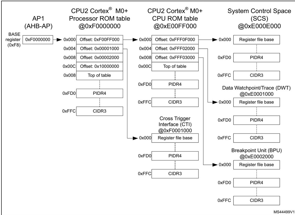
The diagram illustrates the CoreSight topology for the CPU2 subsystem. It shows the following components and their connections:
- AP1 (AHB-AP) : Contains a BASE register (0xF8) with the value 0xF0000000 . This register points to the CPU2 Cortex® M0+ Processor ROM table @0xF0000000 .
- CPU2 Cortex® M0+ Processor ROM table @0xF0000000 : A table with entries at offsets 0x000, 0x004, 0x008, and 0x00C. The entry at 0x008 is marked as the Top of table . This table points to the CPU2 Cortex® M0+ CPU ROM table @0xE00FF000 .
- CPU2 Cortex® M0+ CPU ROM table @0xE00FF000 : A table with entries at offsets 0x000, 0x004, 0x008, and 0x00C. The entry at 0x00C is marked as the Top of table . This table points to the Cross Trigger Interface (CTI) @0xF0001000 .
- Cross Trigger Interface (CTI) @0xF0001000 : Contains a Register file base at offset 0x000, PIDR4 at offset 0xFD0, and CIDR3 at offset 0xFFC.
- System Control Space (SCS) @0xE000E000
: Contains several components:
- Register file base at offset 0x000.
- PIDR4 at offset 0xFD0.
- CIDR3 at offset 0xFFC.
- Data Watchpoint/Trace (DWT) @0xE0001000 : Contains a Register file base at offset 0x000, PIDR4 at offset 0xFD0, and CIDR3 at offset 0xFFC.
- Breakpoint Unit (BPU) @0xE0002000 : Contains a Register file base at offset 0x000, PIDR4 at offset 0xFD0, and CIDR3 at offset 0xFFC.
The diagram also shows connections from the ROM tables to the SCS components and from the CTI to the SCS components. The label MS44499V1 is present in the bottom right corner.
33.9.1 CPU2 ROM1 memory type register (C2ROM1_MEMTYPE)
Address offset: 0xFCC
Reset value: 0x0000 0001
| 31 | 30 | 29 | 28 | 27 | 26 | 25 | 24 | 23 | 22 | 21 | 20 | 19 | 18 | 17 | 16 |
|---|---|---|---|---|---|---|---|---|---|---|---|---|---|---|---|
| Res. | Res. | Res. | Res. | Res. | Res. | Res. | Res. | Res. | Res. | Res. | Res. | Res. | Res. | Res. | Res. |
| 15 | 14 | 13 | 12 | 11 | 10 | 9 | 8 | 7 | 6 | 5 | 4 | 3 | 2 | 1 | 0 |
| Res. | Res. | Res. | Res. | Res. | Res. | Res. | Res. | Res. | Res. | Res. | Res. | Res. | Res. | Res. | SYSMEM |
| rw |
Bits 31:1 Reserved, must be kept at reset value.
Bit 0 SYSMEM : System memory
0x1: System memory is present on this bus
33.9.2 CPU2 ROM1 CoreSight peripheral identity register 4 (C2ROM1_PIDR4)
Address offset: 0xFD0
Reset value: 0x0000 0004
| 31 | 30 | 29 | 28 | 27 | 26 | 25 | 24 | 23 | 22 | 21 | 20 | 19 | 18 | 17 | 16 |
|---|---|---|---|---|---|---|---|---|---|---|---|---|---|---|---|
| Res. | Res. | Res. | Res. | Res. | Res. | Res. | Res. | Res. | Res. | Res. | Res. | Res. | Res. | Res. | Res. |
| 15 | 14 | 13 | 12 | 11 | 10 | 9 | 8 | 7 | 6 | 5 | 4 | 3 | 2 | 1 | 0 |
| Res. | Res. | Res. | Res. | Res. | Res. | Res. | Res. | 4KCOUNT[3:0] | JEP106CON[3:0] | ||||||
| r | r | r | r | r | r | r | r | ||||||||
Bits 31:8 Reserved, must be kept at reset value.
Bits 7:4 4KCOUNT[3:0] : register file size
0x0: Register file occupies a single 4 KB region
Bits 3:0 JEP106CON[3:0] : JEP106 continuation code
0x4: Arm ® JEDEC continuation code
33.9.3 CPU2 ROM1 CoreSight peripheral identity register 0 (C2ROM1_PIDR0)
Address offset: 0xFE0
Reset value: 0x0000 0C0
| 31 | 30 | 29 | 28 | 27 | 26 | 25 | 24 | 23 | 22 | 21 | 20 | 19 | 18 | 17 | 16 |
|---|---|---|---|---|---|---|---|---|---|---|---|---|---|---|---|
| Res. | Res. | Res. | Res. | Res. | Res. | Res. | Res. | Res. | Res. | Res. | Res. | Res. | Res. | Res. | Res. |
| 15 | 14 | 13 | 12 | 11 | 10 | 9 | 8 | 7 | 6 | 5 | 4 | 3 | 2 | 1 | 0 |
| Res. | Res. | Res. | Res. | Res. | Res. | Res. | Res. | PARTNUM[7:0] | |||||||
| r | r | r | r | r | r | r | r | ||||||||
Bits 31:8 Reserved, must be kept at reset value.
Bits 7:0 PARTNUM[7:0] : Part number bits [7:0]
0xC0: Cortex ® -M0+ processor ROM table
33.9.4 CPU2 ROM1 CoreSight peripheral identity register 1 (C2ROM1_PIDR1)
Address offset: 0xFE4
Reset value: 0x0000 00B4
| 31 | 30 | 29 | 28 | 27 | 26 | 25 | 24 | 23 | 22 | 21 | 20 | 19 | 18 | 17 | 16 |
|---|---|---|---|---|---|---|---|---|---|---|---|---|---|---|---|
| Res. | Res. | Res. | Res. | Res. | Res. | Res. | Res. | Res. | Res. | Res. | Res. | Res. | Res. | Res. | Res. |
| 15 | 14 | 13 | 12 | 11 | 10 | 9 | 8 | 7 | 6 | 5 | 4 | 3 | 2 | 1 | 0 |
| Res. | Res. | Res. | Res. | Res. | Res. | Res. | Res. | JEP106ID[3:0] | PARTNUM[11:8] | ||||||
Bit 31:8 Reserved, must be kept at reset value.
Bits 7:4 JEP106ID[3:0] : JEP106 identity code bits [3:0]
0xB: Arm ® JEDEC code
Bits 3:0 PARTNUM[11:8] : Part number bits [11:8]
0x4: Cortex ® -M0+processor ROM table
33.9.5 CPU2 ROM1 CoreSight peripheral identity register 2 (C2ROM1_PIDR2)
Address offset: 0xFE8
Reset value: 0x0000 000B
| 31 | 30 | 29 | 28 | 27 | 26 | 25 | 24 | 23 | 22 | 21 | 20 | 19 | 18 | 17 | 16 |
|---|---|---|---|---|---|---|---|---|---|---|---|---|---|---|---|
| Res. | Res. | Res. | Res. | Res. | Res. | Res. | Res. | Res. | Res. | Res. | Res. | Res. | Res. | Res. | Res. |
| 15 | 14 | 13 | 12 | 11 | 10 | 9 | 8 | 7 | 6 | 5 | 4 | 3 | 2 | 1 | 0 |
| Res. | Res. | Res. | Res. | Res. | Res. | Res. | Res. | REVISION[3:0] | JEDEC | JEP106ID[6:4] | |||||
Bit 31:8 Reserved, must be kept at reset value.
Bits 7:4 REVISION[3:0] : Component revision number
0x0: rev r0p0
Bit 3 JEDEC : JEDEC assigned value
0x1: Designer ID specified by JEDEC
Bits 2:0 JEP106ID[6:4] : JEP106 identity code bits [6:4]
0x3: Arm® JEDEC code
33.9.6 CPU2 ROM1 CoreSight peripheral identity register 3 (C2ROM1_PIDR3)
Address offset: 0xFEC
Reset value: 0x0000 0000
| 31 | 30 | 29 | 28 | 27 | 26 | 25 | 24 | 23 | 22 | 21 | 20 | 19 | 18 | 17 | 16 |
|---|---|---|---|---|---|---|---|---|---|---|---|---|---|---|---|
| Res. | Res. | Res. | Res. | Res. | Res. | Res. | Res. | Res. | Res. | Res. | Res. | Res. | Res. | Res. | Res. |
| 15 | 14 | 13 | 12 | 11 | 10 | 9 | 8 | 7 | 6 | 5 | 4 | 3 | 2 | 1 | 0 |
| Res. | Res. | Res. | Res. | Res. | Res. | Res. | Res. | REVAND[3:0] | CMOD[3:0] | ||||||
| r | r | r | r | r | r | r | r | ||||||||
Bit 31:8 Reserved, must be kept at reset value.
Bits 7:4 REVAND[3:0] : metal fix version
0x0: No metal fix
Bits 3:0 CMOD[3:0] : Customer modified
0x0: No customer modifications
33.9.7 CPU2 ROM1 CoreSight component identity register 0 (C2ROM1_CIDR0)
Address offset: 0xFF0
Reset value: 0x0000 000D
| 31 | 30 | 29 | 28 | 27 | 26 | 25 | 24 | 23 | 22 | 21 | 20 | 19 | 18 | 17 | 16 |
|---|---|---|---|---|---|---|---|---|---|---|---|---|---|---|---|
| Res. | Res. | Res. | Res. | Res. | Res. | Res. | Res. | Res. | Res. | Res. | Res. | Res. | Res. | Res. | Res. |
| 15 | 14 | 13 | 12 | 11 | 10 | 9 | 8 | 7 | 6 | 5 | 4 | 3 | 2 | 1 | 0 |
| Res. | Res. | Res. | Res. | Res. | Res. | Res. | Res. | PREAMBLE[7:0] | |||||||
| r | r | r | r | r | r | r | r | ||||||||
Bits 31:8 Reserved, must be kept at reset value.
Bits 7:0 PREAMBLE[7:0] : Component ID bits [7:0]
0x0D: Common ID value
33.9.8 CPU2 ROM1 CoreSight peripheral identity register 1 (C2ROM1_CIDR1)
Address offset: 0xFF4
Reset value: 0x0000 0010
| 31 | 30 | 29 | 28 | 27 | 26 | 25 | 24 | 23 | 22 | 21 | 20 | 19 | 18 | 17 | 16 |
|---|---|---|---|---|---|---|---|---|---|---|---|---|---|---|---|
| Res. | Res. | Res. | Res. | Res. | Res. | Res. | Res. | Res. | Res. | Res. | Res. | Res. | Res. | Res. | Res. |
| 15 | 14 | 13 | 12 | 11 | 10 | 9 | 8 | 7 | 6 | 5 | 4 | 3 | 2 | 1 | 0 |
| Res. | Res. | Res. | Res. | Res. | Res. | Res. | Res. | CLASS[3:0] | PREAMBLE[11:8] | ||||||
| r | r | r | r | r | r | r | r | ||||||||
Bit 31:8 Reserved, must be kept at reset value.
Bits 7:4
CLASS[3:0]
: Component ID bits [15:12] - component class
0x1: ROM table component
Bits 3:0
PREAMBLE[11:8]
: Component ID bits [11:8]
0x0: Common ID value
33.9.9 CPU2 ROM1 CoreSight component identity register 2 (C2ROM1_CIDR2)
Address offset: 0xFF8
Reset value: 0x0000 0005
| 31 | 30 | 29 | 28 | 27 | 26 | 25 | 24 | 23 | 22 | 21 | 20 | 19 | 18 | 17 | 16 |
|---|---|---|---|---|---|---|---|---|---|---|---|---|---|---|---|
| Res. | Res. | Res. | Res. | Res. | Res. | Res. | Res. | Res. | Res. | Res. | Res. | Res. | Res. | Res. | Res. |
| 15 | 14 | 13 | 12 | 11 | 10 | 9 | 8 | 7 | 6 | 5 | 4 | 3 | 2 | 1 | 0 |
| Res. | Res. | Res. | Res. | Res. | Res. | Res. | Res. | PREAMBLE[19:12] | |||||||
| r | r | r | r | r | r | r | r | ||||||||
Bits 31:8 Reserved, must be kept at reset value.
Bits 7:0
PREAMBLE[19:12]
: Component ID bits [23:16]
0x05: Common ID value
33.9.10 CPU2 ROM1 CoreSight component identity register 3 (C2ROM1_CIDR3)
Address offset: 0xFFC
Reset value: 0x0000 00B1
| 31 | 30 | 29 | 28 | 27 | 26 | 25 | 24 | 23 | 22 | 21 | 20 | 19 | 18 | 17 | 16 |
|---|---|---|---|---|---|---|---|---|---|---|---|---|---|---|---|
| Res. | Res. | Res. | Res. | Res. | Res. | Res. | Res. | Res. | Res. | Res. | Res. | Res. | Res. | Res. | Res. |
| 15 | 14 | 13 | 12 | 11 | 10 | 9 | 8 | 7 | 6 | 5 | 4 | 3 | 2 | 1 | 0 |
| Res. | Res. | Res. | Res. | Res. | Res. | Res. | Res. | PREAMBLE[27:20] | |||||||
| r | r | r | r | r | r | r | r | ||||||||
Bits 31:8 Reserved, must be kept at reset value.
Bits 7:0 PREAMBLE[27:20] : Component ID bits [31:24]
0xB1: Common ID value
33.9.11 CPU2 processor ROM table registers and reset values
Table 222. CPU2 processor ROM table register map and reset values
| Offset | Register name | 31 | 30 | 29 | 28 | 27 | 26 | 25 | 24 | 23 | 22 | 21 | 20 | 19 | 18 | 17 | 16 | 15 | 14 | 13 | 12 | 11 | 10 | 9 | 8 | 7 | 6 | 5 | 4 | 3 | 2 | 1 | 0 | |
|---|---|---|---|---|---|---|---|---|---|---|---|---|---|---|---|---|---|---|---|---|---|---|---|---|---|---|---|---|---|---|---|---|---|---|
| 0xFCC | C2ROM1_MEMTYPER | Res. | Res. | Res. | Res. | Res. | Res. | Res. | Res. | Res. | Res. | Res. | Res. | Res. | Res. | Res. | Res. | Res. | Res. | Res. | Res. | Res. | Res. | Res. | Res. | Res. | Res. | Res. | Res. | Res. | Res. | Res. | Res. | SYSTEM |
| Reset value | 1 | |||||||||||||||||||||||||||||||||
| 0xFD0 | C2ROM1_PIDR4 | Res. | Res. | Res. | Res. | Res. | Res. | Res. | Res. | Res. | Res. | Res. | Res. | Res. | Res. | Res. | Res. | Res. | Res. | Res. | Res. | Res. | Res. | Res. | Res. | Res. | 4KCOUNT [3:0] | JEP106CON [3:0] | ||||||
| Reset value | 0 | 0 | 0 | 0 | 0 | 1 | 0 | 0 | ||||||||||||||||||||||||||
| 0xFE0 | C2ROM1_PIDR0 | Res. | Res. | Res. | Res. | Res. | Res. | Res. | Res. | Res. | Res. | Res. | Res. | Res. | Res. | Res. | Res. | Res. | Res. | Res. | Res. | Res. | Res. | Res. | Res. | PARTNUM[7:0] | ||||||||
| Reset value | 1 | 1 | 0 | 0 | 0 | 0 | 0 | 0 | ||||||||||||||||||||||||||
| 0xFE4 | C2ROM1_PIDR1 | Res. | Res. | Res. | Res. | Res. | Res. | Res. | Res. | Res. | Res. | Res. | Res. | Res. | Res. | Res. | Res. | Res. | Res. | Res. | Res. | Res. | Res. | Res. | Res. | JEP106ID [3:0] | PARTNUM [11:8] | |||||||
| Reset value | 1 | 0 | 1 | 1 | 0 | 1 | 0 | 0 | ||||||||||||||||||||||||||
| 0xFE8 | C2ROM1_PIDR2 | Res. | Res. | Res. | Res. | Res. | Res. | Res. | Res. | Res. | Res. | Res. | Res. | Res. | Res. | Res. | Res. | Res. | Res. | Res. | Res. | Res. | Res. | Res. | Res. | REVISION [3:0] | JEDEC | JEP106ID [6:4] | ||||||
| Reset value | 0 | 0 | 0 | 0 | 1 | 0 | 1 | 1 | ||||||||||||||||||||||||||
| 0xFEC | C2ROM1_PIDR3 | Res. | Res. | Res. | Res. | Res. | Res. | Res. | Res. | Res. | Res. | Res. | Res. | Res. | Res. | Res. | Res. | Res. | Res. | Res. | Res. | Res. | Res. | Res. | Res. | REVAND[3:0] | CMOD[3:0] | |||||||
| Reset value | 0 | 0 | 0 | 0 | 0 | 0 | 0 | 0 | ||||||||||||||||||||||||||
| 0xFF0 | C2ROM1_CIDR0 | Res. | Res. | Res. | Res. | Res. | Res. | Res. | Res. | Res. | Res. | Res. | Res. | Res. | Res. | Res. | Res. | Res. | Res. | Res. | Res. | Res. | Res. | Res. | Res. | PREAMBLE[7:0] | ||||||||
| Reset value | 0 | 0 | 0 | 0 | 1 | 1 | 0 | 1 | ||||||||||||||||||||||||||
| 0xFF4 | C2ROM1_CIDR1 | Res. | Res. | Res. | Res. | Res. | Res. | Res. | Res. | Res. | Res. | Res. | Res. | Res. | Res. | Res. | Res. | Res. | Res. | Res. | Res. | Res. | Res. | Res. | Res. | CLASS[3:0] | PREAMBLE [11:8] | |||||||
| Reset value | 0 | 0 | 0 | 1 | 0 | 0 | 0 | 0 | ||||||||||||||||||||||||||
| 0xFF8 | C2ROM1_CIDR2 | Res. | Res. | Res. | Res. | Res. | Res. | Res. | Res. | Res. | Res. | Res. | Res. | Res. | Res. | Res. | Res. | Res. | Res. | Res. | Res. | Res. | Res. | Res. | Res. | PREAMBLE[19:12] | ||||||||
| Reset value | 0 | 0 | 0 | 0 | 0 | 1 | 0 | 1 | ||||||||||||||||||||||||||
| 0xFFC | C2ROM1_CIDR3 | Res. | Res. | Res. | Res. | Res. | Res. | Res. | Res. | Res. | Res. | Res. | Res. | Res. | Res. | Res. | Res. | Res. | Res. | Res. | Res. | Res. | Res. | Res. | Res. | PREAMBLE[27:20] | ||||||||
| Reset value | 1 | 0 | 1 | 1 | 0 | 0 | 0 | 1 | ||||||||||||||||||||||||||
Refer to Section 33.9: CPU2 ROM tables for the register boundary addresses.
33.9.12 CPU2 ROM2 memory type register (C2ROM2_MEMTYPER)
Address offset: 0xFCC
Reset value: 0x0000 0001
| 31 | 30 | 29 | 28 | 27 | 26 | 25 | 24 | 23 | 22 | 21 | 20 | 19 | 18 | 17 | 16 |
|---|---|---|---|---|---|---|---|---|---|---|---|---|---|---|---|
| Res. | Res. | Res. | Res. | Res. | Res. | Res. | Res. | Res. | Res. | Res. | Res. | Res. | Res. | Res. | Res. |
| 15 | 14 | 13 | 12 | 11 | 10 | 9 | 8 | 7 | 6 | 5 | 4 | 3 | 2 | 1 | 0 |
| Res. | Res. | Res. | Res. | Res. | Res. | Res. | Res. | Res. | Res. | Res. | Res. | Res. | Res. | Res. | SYSTEM |
| rw |
Bits 31:1 Reserved, must be kept at reset value.
Bit 0 SYSTEM : System memory
0x1: System memory is present on this bus
33.9.13 CPU2 ROM2 CoreSight peripheral identity register 4 (C2ROM2_PIDR4)
Address offset: 0xFD0
Reset value: 0x0000 0004
| 31 | 30 | 29 | 28 | 27 | 26 | 25 | 24 | 23 | 22 | 21 | 20 | 19 | 18 | 17 | 16 |
|---|---|---|---|---|---|---|---|---|---|---|---|---|---|---|---|
| Res. | Res. | Res. | Res. | Res. | Res. | Res. | Res. | Res. | Res. | Res. | Res. | Res. | Res. | Res. | Res. |
| 15 | 14 | 13 | 12 | 11 | 10 | 9 | 8 | 7 | 6 | 5 | 4 | 3 | 2 | 1 | 0 |
| Res. | Res. | Res. | Res. | Res. | Res. | Res. | Res. | 4KCOUNT[3:0] | JEP106CON[3:0] | ||||||
| r | r | r | r | r | r | r | r | ||||||||
Bits 31:8 Reserved, must be kept at reset value.
Bits 7:4 4KCOUNT[3:0] : register file size
0x0: Register file occupies a single 4 KB region
Bits 3:0 JEP106CON[3:0] : JEP106 continuation code
0x4: Arm® JEDEC continuation code
33.9.14 CPU2 ROM2 CoreSight peripheral identity register 0 (C2ROM2_PIDR0)
Address offset: 0xFE0
Reset value: 0x0000 0C0
| 31 | 30 | 29 | 28 | 27 | 26 | 25 | 24 | 23 | 22 | 21 | 20 | 19 | 18 | 17 | 16 |
|---|---|---|---|---|---|---|---|---|---|---|---|---|---|---|---|
| Res. | Res. | Res. | Res. | Res. | Res. | Res. | Res. | Res. | Res. | Res. | Res. | Res. | Res. | Res. | Res. |
| 15 | 14 | 13 | 12 | 11 | 10 | 9 | 8 | 7 | 6 | 5 | 4 | 3 | 2 | 1 | 0 |
| Res. | Res. | Res. | Res. | Res. | Res. | Res. | Res. | PARTNUM[7:0] | |||||||
| r | r | r | r | r | r | r | r | ||||||||
Bits 31:8 Reserved, must be kept at reset value.
Bits 7:0 PARTNUM[7:0] : Part number bits [7:0]
0xC0: CPU2 ROM table
33.9.15 CPU2 ROM2 CoreSight peripheral identity register 1 (C2ROM2_PIDR1)
Address offset: 0xFE4
Reset value: 0x0000 00B4
| 31 | 30 | 29 | 28 | 27 | 26 | 25 | 24 | 23 | 22 | 21 | 20 | 19 | 18 | 17 | 16 |
|---|---|---|---|---|---|---|---|---|---|---|---|---|---|---|---|
| Res. | Res. | Res. | Res. | Res. | Res. | Res. | Res. | Res. | Res. | Res. | Res. | Res. | Res. | Res. | Res. |
| 15 | 14 | 13 | 12 | 11 | 10 | 9 | 8 | 7 | 6 | 5 | 4 | 3 | 2 | 1 | 0 |
| Res. | Res. | Res. | Res. | Res. | Res. | Res. | Res. | JEP106ID[3:0] | PARTNUM[11:8] | ||||||
| r | r | r | r | r | r | r | r | ||||||||
Bit 31:8 Reserved, must be kept at reset value.
Bits 7:4 JEP106ID[3:0] : JEP106 identity code bits [3:0]
0xB: Arm® JEDEC code
Bits 3:0 PARTNUM[11:8] : Part number bits [11:8]
0x4: CPU2 ROM table
33.9.16 CPU2 ROM2 CoreSight peripheral identity register 2 (C2ROM2_PIDR2)
Address offset: 0xFE8
Reset value: 0x0000 000B
| 31 | 30 | 29 | 28 | 27 | 26 | 25 | 24 | 23 | 22 | 21 | 20 | 19 | 18 | 17 | 16 |
|---|---|---|---|---|---|---|---|---|---|---|---|---|---|---|---|
| Res. | Res. | Res. | Res. | Res. | Res. | Res. | Res. | Res. | Res. | Res. | Res. | Res. | Res. | Res. | Res. |
| 15 | 14 | 13 | 12 | 11 | 10 | 9 | 8 | 7 | 6 | 5 | 4 | 3 | 2 | 1 | 0 |
| Res. | Res. | Res. | Res. | Res. | Res. | Res. | Res. | REVISION[3:0] | JEDEC | JEP106ID[6:4] | |||||
| r | r | r | r | r | r | r | r | ||||||||
Bit 31:8 Reserved, must be kept at reset value.
Bits 7:4 REVISION[3:0] : Component revision number
0x0: rev r0p0
Bit 3 JEDEC : JEDEC assigned value
0x1: Designer ID specified by JEDEC
Bits 2:0 JEP106ID[6:4] : JEP106 identity code bits [6:4]
0x3: Arm® JEDEC code
33.9.17 CPU2 ROM2 CoreSight peripheral identity register 3 (C2ROM2_PIDR3)
Address offset: 0xFEC
Reset value: 0x0000 0000
| 31 | 30 | 29 | 28 | 27 | 26 | 25 | 24 | 23 | 22 | 21 | 20 | 19 | 18 | 17 | 16 |
|---|---|---|---|---|---|---|---|---|---|---|---|---|---|---|---|
| Res. | Res. | Res. | Res. | Res. | Res. | Res. | Res. | Res. | Res. | Res. | Res. | Res. | Res. | Res. | Res. |
| 15 | 14 | 13 | 12 | 11 | 10 | 9 | 8 | 7 | 6 | 5 | 4 | 3 | 2 | 1 | 0 |
| Res. | Res. | Res. | Res. | Res. | Res. | Res. | Res. | REVAND[3:0] | CMOD[3:0] | ||||||
| r | r | r | r | r | r | r | r | ||||||||
Bit 31:8 Reserved, must be kept at reset value.
Bits 7:4 REVAND[3:0] : metal fix version
0x0: No metal fix
Bits 3:0 CMOD[3:0] : Customer modified
0x0: No customer modifications
33.9.18 CPU2 ROM2 CoreSight component identity register 0 (C2ROM2_CIDR0)
Address offset: 0xFF0
Reset value: 0x0000 000D
| 31 | 30 | 29 | 28 | 27 | 26 | 25 | 24 | 23 | 22 | 21 | 20 | 19 | 18 | 17 | 16 |
|---|---|---|---|---|---|---|---|---|---|---|---|---|---|---|---|
| Res. | Res. | Res. | Res. | Res. | Res. | Res. | Res. | Res. | Res. | Res. | Res. | Res. | Res. | Res. | Res. |
| 15 | 14 | 13 | 12 | 11 | 10 | 9 | 8 | 7 | 6 | 5 | 4 | 3 | 2 | 1 | 0 |
| Res. | Res. | Res. | Res. | Res. | Res. | Res. | Res. | PREAMBLE[7:0] | |||||||
| r | r | r | r | r | r | r | r | ||||||||
Bits 31:8 Reserved, must be kept at reset value.
Bits 7:0 PREAMBLE[7:0] : Component ID bits [7:0]
0x0D: Common ID value
33.9.19 CPU2 ROM2 CoreSight peripheral identity register 1 (C2ROM2_CIDR1)
Address offset: 0xFF4
Reset value: 0x0000 0010
| 31 | 30 | 29 | 28 | 27 | 26 | 25 | 24 | 23 | 22 | 21 | 20 | 19 | 18 | 17 | 16 |
| Res. | Res. | Res. | Res. | Res. | Res. | Res. | Res. | Res. | Res. | Res. | Res. | Res. | Res. | Res. | Res. |
| 15 | 14 | 13 | 12 | 11 | 10 | 9 | 8 | 7 | 6 | 5 | 4 | 3 | 2 | 1 | 0 |
| Res. | Res. | Res. | Res. | Res. | Res. | Res. | Res. | CLASS[3:0] | PREAMBLE[11:8] | ||||||
| r | r | r | r | r | r | r | r | ||||||||
Bit 31:8 Reserved, must be kept at reset value.
Bits 7:4
CLASS[3:0]
: Component ID bits [15:12] - component class
0x1: ROM table component
Bits 3:0
PREAMBLE[11:8]
: Component ID bits [11:8]
0x0: Common ID value
33.9.20 CPU2 ROM2 CoreSight component identity register 2 (C2ROM2_CIDR2)
Address offset: 0xFF8
Reset value: 0x0000 0005
| 31 | 30 | 29 | 28 | 27 | 26 | 25 | 24 | 23 | 22 | 21 | 20 | 19 | 18 | 17 | 16 |
| Res. | Res. | Res. | Res. | Res. | Res. | Res. | Res. | Res. | Res. | Res. | Res. | Res. | Res. | Res. | Res. |
| 15 | 14 | 13 | 12 | 11 | 10 | 9 | 8 | 7 | 6 | 5 | 4 | 3 | 2 | 1 | 0 |
| Res. | Res. | Res. | Res. | Res. | Res. | Res. | Res. | PREAMBLE[19:12] | |||||||
| r | r | r | r | r | r | r | r | ||||||||
Bits 31:8 Reserved, must be kept at reset value.
Bits 7:0
PREAMBLE[19:12]
: Component ID bits [23:16]
0x05: Common ID value
33.9.21 CPU2 ROM2 CoreSight component identity register 3 (C2ROM2_CIDR3)
Address offset: 0xFFC
Reset value: 0x0000 00B1
| 31 | 30 | 29 | 28 | 27 | 26 | 25 | 24 | 23 | 22 | 21 | 20 | 19 | 18 | 17 | 16 |
|---|---|---|---|---|---|---|---|---|---|---|---|---|---|---|---|
| Res. | Res. | Res. | Res. | Res. | Res. | Res. | Res. | Res. | Res. | Res. | Res. | Res. | Res. | Res. | Res. |
| 15 | 14 | 13 | 12 | 11 | 10 | 9 | 8 | 7 | 6 | 5 | 4 | 3 | 2 | 1 | 0 |
| Res. | Res. | Res. | Res. | Res. | Res. | Res. | Res. | PREAMBLE[27:20] | |||||||
| 3r | r | r | r | r | r | r | r | ||||||||
Bits 31:8 Reserved, must be kept at reset value.
Bits 7:0 PREAMBLE[27:20] : Component ID bits [31:24]
0xB1: Common ID value
33.9.22 CPU2 ROM table register map and reset values
Table 223. CPU2 ROM table register map and reset values
| Offset | Register name | 31 | 30 | 29 | 28 | 27 | 26 | 25 | 24 | 23 | 22 | 21 | 20 | 19 | 18 | 17 | 16 | 15 | 14 | 13 | 12 | 11 | 10 | 9 | 8 | 7 | 6 | 5 | 4 | 3 | 2 | 1 | 0 | |
|---|---|---|---|---|---|---|---|---|---|---|---|---|---|---|---|---|---|---|---|---|---|---|---|---|---|---|---|---|---|---|---|---|---|---|
| 0xFCC | C2ROM2_MEMTYPER | Res. | Res. | Res. | Res. | Res. | Res. | Res. | Res. | Res. | Res. | Res. | Res. | Res. | Res. | Res. | Res. | Res. | Res. | Res. | Res. | Res. | Res. | Res. | Res. | Res. | Res. | Res. | Res. | Res. | Res. | Res. | Res. | SYSTEM |
| Reset value | 1 | |||||||||||||||||||||||||||||||||
| 0xFD0 | C2ROM2_PIDR4 | Res. | Res. | Res. | Res. | Res. | Res. | Res. | Res. | Res. | Res. | Res. | Res. | Res. | Res. | Res. | Res. | Res. | Res. | Res. | Res. | Res. | Res. | Res. | Res. | Res. | 4KCOUNT [3:0] | JEP106CON[3:0] | ||||||
| Reset value | 0 | 0 | 0 | 0 | 0 | 1 | 0 | 0 | ||||||||||||||||||||||||||
| 0xFE0 | C2ROM2_PIDR0 | Res. | Res. | Res. | Res. | Res. | Res. | Res. | Res. | Res. | Res. | Res. | Res. | Res. | Res. | Res. | Res. | Res. | Res. | Res. | Res. | Res. | Res. | Res. | Res. | PARTNUM[7:0] | ||||||||
| Reset value | 1 | 1 | 0 | 0 | 0 | 0 | 0 | 0 | ||||||||||||||||||||||||||
| 0xFE4 | C2ROM2_PIDR1 | Res. | Res. | Res. | Res. | Res. | Res. | Res. | Res. | Res. | Res. | Res. | Res. | Res. | Res. | Res. | Res. | Res. | Res. | Res. | Res. | Res. | Res. | Res. | Res. | JEP106ID [3:0] | PARTNUM [11:8] | |||||||
| Reset value | 1 | 0 | 1 | 1 | 0 | 1 | 0 | 0 | ||||||||||||||||||||||||||
| 0xFE8 | C2ROM2_PIDR2 | Res. | Res. | Res. | Res. | Res. | Res. | Res. | Res. | Res. | Res. | Res. | Res. | Res. | Res. | Res. | Res. | Res. | Res. | Res. | Res. | Res. | Res. | Res. | Res. | REVISION [3:0] | JEDEC | JEP106ID [6:4] | ||||||
| Reset value | 0 | 0 | 0 | 0 | 1 | 0 | 1 | 1 | ||||||||||||||||||||||||||
| 0xFEC | C2ROM2_PIDR3 | Res. | Res. | Res. | Res. | Res. | Res. | Res. | Res. | Res. | Res. | Res. | Res. | Res. | Res. | Res. | Res. | Res. | Res. | Res. | Res. | Res. | Res. | Res. | Res. | REVAND[3:0] | CMOD[3:0] | |||||||
| Reset value | 0 | 0 | 0 | 0 | 0 | 0 | 0 | 0 | ||||||||||||||||||||||||||
| 0xFF0 | C2ROM2_CIDR0 | Res. | Res. | Res. | Res. | Res. | Res. | Res. | Res. | Res. | Res. | Res. | Res. | Res. | Res. | Res. | Res. | Res. | Res. | Res. | Res. | Res. | Res. | Res. | Res. | PREAMBLE[7:0] | ||||||||
| Reset value | 0 | 0 | 0 | 0 | 1 | 1 | 0 | 1 | ||||||||||||||||||||||||||
| 0xFF4 | C2ROM2_CIDR1 | Res. | Res. | Res. | Res. | Res. | Res. | Res. | Res. | Res. | Res. | Res. | Res. | Res. | Res. | Res. | Res. | Res. | Res. | Res. | Res. | Res. | Res. | Res. | Res. | CLASS[3:0] | PREAMBLE [11:8] | |||||||
| Reset value | 0 | 0 | 0 | 1 | 0 | 0 | 0 | 0 | ||||||||||||||||||||||||||
| 0xFF8 | C2ROM2_CIDR2 | Res. | Res. | Res. | Res. | Res. | Res. | Res. | Res. | Res. | Res. | Res. | Res. | Res. | Res. | Res. | Res. | Res. | Res. | Res. | Res. | Res. | Res. | Res. | Res. | PREAMBLE[19:12] | ||||||||
| Reset value | 0 | 0 | 0 | 0 | 0 | 1 | 0 | 1 | ||||||||||||||||||||||||||
| 0xFFC | C2ROM2_CIDR3 | Res. | Res. | Res. | Res. | Res. | Res. | Res. | Res. | Res. | Res. | Res. | Res. | Res. | Res. | Res. | Res. | Res. | Res. | Res. | Res. | Res. | Res. | Res. | Res. | PREAMBLE[27:20] | ||||||||
| Reset value | 1 | 0 | 1 | 1 | 0 | 0 | 0 | 1 | ||||||||||||||||||||||||||
Refer to Section 33.9: CPU2 ROM tables for the register boundary addresses.
33.10 CPU2 data watchpoint and trace unit (DWT)
The DWT provides four comparators that can be used as:
- • Watchpoint
- • PC sampling trigger
- • Data address sampling trigger
- • Data comparator (for comparator 1 only)
- • Clock cycle counter comparator (for comparator 0 only)
It also contains counters for:
- • Clock cycles
- • Folded instructions
- • Load store unit (LSU) operations
- • Sleep cycles
- • Number of cycles per instruction
- • Interrupt overhead
A DWT comparator compares the value held in its DWT_COMP register with one of the following items:
- • a data address
- • an instruction address
- • a data value
- • the cycle count value (comparator 0 only)
For address matching, the comparator can use a mask, so it matches a range of addresses.
On a successful match, the comparator generates one of the following:
- • One or more DWT Data trace packets, containing one or more of:
- – the address of the instruction that caused a data access
- – an address offset, bits[15:0] of the data access address
- – the matched data value.
- • A watchpoint debug event, on either the PC value or the accessed data address.
- • A CMPMATCH[N] event, that signals the match outside the DWT unit.
A watchpoint debug event either generates a DebugMonitor exception, or causes the processor to halt execution and enter Debug state.
For more details on how to use the DWT, refer to the Arm ® v7-M Architecture Reference Manual [5].
33.10.1 DWT control register (DWT_CTRLR)
Address offset: 0x000
Reset value: 0x4000 0000
| 31 | 30 | 29 | 28 | 27 | 26 | 25 | 24 | 23 | 22 | 21 | 20 | 19 | 18 | 17 | 16 |
|---|---|---|---|---|---|---|---|---|---|---|---|---|---|---|---|
| NUMCOMP[3:0] | NOTRCPKT | NOEXTTRIG | NOCYCCNT | NOPRFCNT | Res. | CYCEVTENA | FOLDEVTEENA | LSUEVTENA | SLEEPEVTENA | EXCEVTENA | CPIEVTENA | EXCTRCENA | |||
| r | r | r | r | r | r | r | r | rw | rw | rw | rw | rw | rw | rw | |
| 15 | 14 | 13 | 12 | 11 | 10 | 9 | 8 | 7 | 6 | 5 | 4 | 3 | 2 | 1 | 0 |
| Res. | Res. | Res. | PCSAMPLENA | SYNCTAP[1:0] | CYCTAP | POSTINIT[3:0] | POSTRESET[3:0] | CYCCNTENA | |||||||
| rw | rw | rw | rw | rw | rw | rw | rw | rw | rw | rw | rw | rw | |||
Bits 31:28 NUMCOMP : Number of comparators implemented (read only)
0x4: Four comparators
Bit 27 NOTRCPKT : Trace sampling and exception tracing support (read only)
0x0: Supported
Bit 26 NOEXTTRIG : External match signal, CMPMATCH support (read only)
0x0: Supported
Bit 25 NOCYCCNT : Cycle counter support (read only)
0x0: Supported
Bit 24 NOPRFCNT : Profiling counter support (read only)
0x0: Supported
Bit 23 Reserved, must be kept at reset value.
Bit 22 CYCEVTENA : Enable for POSTCNT underflow event counter packet generation
0x0: Disabled
0x1: Enabled
Bit 21 FOLDEVTEENA : Enable for folded instruction counter overflow event generation
0x0: Disabled
0x1: Enabled
Bit 20 LSUEVTENA : Enable for LSU counter overflow event generation
0x0: Disabled
0x1: Enabled
Bit 19 SLEEPEVTENA : Enable for sleep counter overflow event generation
0x0: Disabled
0x1: Enabled
Bit 18 EXCEVTENA : Enable for exception overhead counter overflow event generation
0x0: Disabled
0x1: Enabled
Bit 17 CPIEVTENA : Enable for CPI counter overflow event generation
0x0: Disabled
0x1: Enabled
Bit 16 EXCTRCENA : Enable for exception trace generation
0x0: Disabled
0x1: Enabled
Bits 15:13 Reserved, must be kept at reset value.
Bit 12 PCSAMPLENA : Enables use of POSTCNT counter as a timer for Periodic PC sample packet generation.
0x0: Disabled
0x1: Enabled
Bits 11:10 SYNCTAP[1:0] : Selects the position of the synchronization packet counter tap on the CYCCNT counter. This determines the synchronization packet rate.
0x0: Disabled. No synchronization packets
0x1: Tap at CYCCNT[24]
0x2: Tap at CYCCNT[26]
0x3: Tap at CYCCNT[28]
Bit 9 CYCTAP : Selects the position of the POSTCNT tap on the CYCCNT counter.
0x0: Tap at CYCCNT[6]
0x1: Tap at CYCCNT[10]
Bits 8:5 POSTINIT[3:0] : Initial value of the POSTCNT counter. Writes to this field are ignored if POSTCNT counter is enabled (ie. CYCEVTENA or PCSAMPLENA must be reset prior to writing POSTINIT).
Bits 4:1 POSTPRESET[3:0] : Reload value of the POSTCNT counter.
Bit 0 CYCCNTENA : Enables CYCCNT counter.
0x0: Disabled
0x1: Enabled
33.10.2 DWT cycle count register (DWT_CYCCNTR)
Address offset: 0x004
Reset value: 0x0000 0000
| 31 | 30 | 29 | 28 | 27 | 26 | 25 | 24 | 23 | 22 | 21 | 20 | 19 | 18 | 17 | 16 |
| CYCCNT[31:16] | |||||||||||||||
| r | r | r | r | r | r | r | r | r | r | r | r | r | r | r | r |
| 15 | 14 | 13 | 12 | 11 | 10 | 9 | 8 | 7 | 6 | 5 | 4 | 3 | 2 | 1 | 0 |
| CYCCNT[15:0] | |||||||||||||||
| r | r | r | r | r | r | r | r | r | r | r | r | r | r | r | r |
Bits 31:0 CYCCNT[31:0] : Processor clock cycle counter
33.10.3 DWT CPI count register (DWT_CPICNTR)
Address offset: 0x008
Reset value: 0x0000 0000
| 31 | 30 | 29 | 28 | 27 | 26 | 25 | 24 | 23 | 22 | 21 | 20 | 19 | 18 | 17 | 16 |
|---|---|---|---|---|---|---|---|---|---|---|---|---|---|---|---|
| Res. | Res. | Res. | Res. | Res. | Res. | Res. | Res. | Res. | Res. | Res. | Res. | Res. | Res. | Res. | Res. |
| 15 | 14 | 13 | 12 | 11 | 10 | 9 | 8 | 7 | 6 | 5 | 4 | 3 | 2 | 1 | 0 |
| Res. | Res. | Res. | Res. | Res. | Res. | Res. | Res. | CPICNT[7:0] | |||||||
| rw | rw | rw | rw | rw | rw | rw | rw | ||||||||
Bits 31:8 Reserved, must be kept at reset value.
Bits 7:0 CPICNT[7:0] : CPI counter. Counts additional cycles required to execute multi-cycle instructions, except those recorded by DWT_LSUCNTR, and counts any instruction fetch stalls.
33.10.4 DWT exception count register (DWT_EXCCNTR)
Address offset: 0x00C
Reset value: 0x0000 0000
| 31 | 30 | 29 | 28 | 27 | 26 | 25 | 24 | 23 | 22 | 21 | 20 | 19 | 18 | 17 | 16 |
|---|---|---|---|---|---|---|---|---|---|---|---|---|---|---|---|
| Res. | Res. | Res. | Res. | Res. | Res. | Res. | Res. | Res. | Res. | Res. | Res. | Res. | Res. | Res. | Res. |
| 15 | 14 | 13 | 12 | 11 | 10 | 9 | 8 | 7 | 6 | 5 | 4 | 3 | 2 | 1 | 0 |
| Res. | Res. | Res. | Res. | Res. | Res. | Res. | Res. | EXCCNT[7:0] | |||||||
| rw | rw | rw | rw | rw | rw | rw | rw | ||||||||
Bits 31:8 Reserved, must be kept at reset value.
Bits 7:0 EXCCNT[7:0] : Exception overhead cycle counter. Counts the number of cycles spent in exception processing.
33.10.5 DWT sleep count register (DWT_SLP CNTR)
Address offset: 0x010
Reset value: 0x0000 0000
| 31 | 30 | 29 | 28 | 27 | 26 | 25 | 24 | 23 | 22 | 21 | 20 | 19 | 18 | 17 | 16 |
|---|---|---|---|---|---|---|---|---|---|---|---|---|---|---|---|
| Res. | Res. | Res. | Res. | Res. | Res. | Res. | Res. | Res. | Res. | Res. | Res. | Res. | Res. | Res. | Res. |
| 15 | 14 | 13 | 12 | 11 | 10 | 9 | 8 | 7 | 6 | 5 | 4 | 3 | 2 | 1 | 0 |
| Res. | Res. | Res. | Res. | Res. | Res. | Res. | Res. | SLP CNTR[7:0] | |||||||
| rw | rw | rw | rw | rw | rw | rw | rw | ||||||||
Bits 31:8 Reserved, must be kept at reset value.
Bits 7:0 SLP CNTR[7:0] : Sleep cycle counter. Counts the number of cycles spent in sleep mode (WFI, WFE, sleep-on-exit).
33.10.6 DWT LSU count register (DWT_LSUCNTR)
Address offset: 0x014
Reset value: 0x0000 0000
| 31 | 30 | 29 | 28 | 27 | 26 | 25 | 24 | 23 | 22 | 21 | 20 | 19 | 18 | 17 | 16 |
|---|---|---|---|---|---|---|---|---|---|---|---|---|---|---|---|
| Res. | Res. | Res. | Res. | Res. | Res. | Res. | Res. | Res. | Res. | Res. | Res. | Res. | Res. | Res. | Res. |
| 15 | 14 | 13 | 12 | 11 | 10 | 9 | 8 | 7 | 6 | 5 | 4 | 3 | 2 | 1 | 0 |
| Res. | Res. | Res. | Res. | Res. | Res. | Res. | Res. | LSUCNT[7:0] | |||||||
| rw | rw | rw | rw | rw | rw | rw | rw | ||||||||
Bits 31:8 Reserved, must be kept at reset value.
Bits 7:0 LSUCNT[7:0] : Load store counter. Counts additional cycles required to execute load and store instructions.
33.10.7 DWT fold count register (DWT_FOLDCNTR)
Address offset: 0x018
Reset value: 0x0000 0000
| 31 | 30 | 29 | 28 | 27 | 26 | 25 | 24 | 23 | 22 | 21 | 20 | 19 | 18 | 17 | 16 |
|---|---|---|---|---|---|---|---|---|---|---|---|---|---|---|---|
| Res. | Res. | Res. | Res. | Res. | Res. | Res. | Res. | Res. | Res. | Res. | Res. | Res. | Res. | Res. | Res. |
| 15 | 14 | 13 | 12 | 11 | 10 | 9 | 8 | 7 | 6 | 5 | 4 | 3 | 2 | 1 | 0 |
| Res. | Res. | Res. | Res. | Res. | Res. | Res. | Res. | FOLDCNT[7:0] | |||||||
| rw | rw | rw | rw | rw | rw | rw | rw | ||||||||
Bits 31:8 Reserved, must be kept at reset value.
Bits 7:0 FOLDCNT[7:0] : Folded instruction counter. Increments on each instruction that takes 0 cycles.
33.10.8 DWT program counter sample register (DWT_PCSR)
Address offset: 0x01C
Reset value: 0x0000 0000
| 31 | 30 | 29 | 28 | 27 | 26 | 25 | 24 | 23 | 22 | 21 | 20 | 19 | 18 | 17 | 16 |
|---|---|---|---|---|---|---|---|---|---|---|---|---|---|---|---|
| EIASAMPLE[31:16] | |||||||||||||||
| r | r | r | r | r | r | r | r | r | r | r | r | r | r | r | r |
| 15 | 14 | 13 | 12 | 11 | 10 | 9 | 8 | 7 | 6 | 5 | 4 | 3 | 2 | 1 | 0 |
| EIASAMPLE[15:0] | |||||||||||||||
| r | r | r | r | r | r | r | r | r | r | r | r | r | r | r | r |
Bits 31:0 EIASAMPLE[31:0] : Executed Instruction Address sample value. Samples the current value of the program counter.
33.10.9 DWT comparator register x (DWT_COMPxR)
Address offset: 0x020 + x * 0x10 (for x = 0 to 3)
Reset value: 0x0000 0000
| 31 | 30 | 29 | 28 | 27 | 26 | 25 | 24 | 23 | 22 | 21 | 20 | 19 | 18 | 17 | 16 |
|---|---|---|---|---|---|---|---|---|---|---|---|---|---|---|---|
| COMP[31:16] | |||||||||||||||
| r | r | r | r | r | r | r | r | r | r | r | r | r | r | r | r |
| 15 | 14 | 13 | 12 | 11 | 10 | 9 | 8 | 7 | 6 | 5 | 4 | 3 | 2 | 1 | 0 |
| COMP[15:0] | |||||||||||||||
| r | r | r | r | r | r | r | r | r | r | r | r | r | r | r | r |
Bits 31:0 COMP[31:0] : Reference value for comparison.
33.10.10 DWT mask register x (DWT_MASKxR)
Address offset: 0x024 + x * 0x10 (for x = 0 to 3)
Reset value: 0x0000 0000
| 31 | 30 | 29 | 28 | 27 | 26 | 25 | 24 | 23 | 22 | 21 | 20 | 19 | 18 | 17 | 16 |
|---|---|---|---|---|---|---|---|---|---|---|---|---|---|---|---|
| Res. | Res. | Res. | Res. | Res. | Res. | Res. | Res. | Res. | Res. | Res. | Res. | Res. | Res. | Res. | Res. |
| 15 | 14 | 13 | 12 | 11 | 10 | 9 | 8 | 7 | 6 | 5 | 4 | 3 | 2 | 1 | 0 |
| Res. | Res. | Res. | Res. | Res. | Res. | Res. | Res. | Res. | Res. | Res. | MASK[4:0] | ||||
| rw | rw | rw | rw | rw | |||||||||||
Bits 31:5 Reserved, must be kept at reset value.
Bits 4:0 MASK[4:0] : Comparator mask size. Provides the size of the ignore mask applied to the access address for address range matching by comparator n. A debugger can write 0b11111 to this field and then read the register back to determine the maximum mask size supported.
33.10.11 DWT function register x (DWT_FUNCTxR)
Address offset: 0x028 + x * 0x10 (for x = 0 to 3)
Reset value: 0x0000 0000
| 31 | 30 | 29 | 28 | 27 | 26 | 25 | 24 | 23 | 22 | 21 | 20 | 19 | 18 | 17 | 16 |
|---|---|---|---|---|---|---|---|---|---|---|---|---|---|---|---|
| Res. | Res. | Res. | Res. | Res. | Res. | Res. | MATCHED | Res. | Res. | Res. | Res. | DATAVADDR1[3:0] | |||
| r | rw | rw | rw | rw | |||||||||||
| 15 | 14 | 13 | 12 | 11 | 10 | 9 | 8 | 7 | 6 | 5 | 4 | 3 | 2 | 1 | 0 |
| DATAVADDR0[3:0] | DATAVSIZE[1:0] | LINK1ENA | DATAVMATCH | CYCMATCH | Res. | EMITRANGE | Res. | FUNCTION[3:0] | |||||||
| rw | rw | rw | rw | rw | rw | rw | rw | rw | rw | rw | rw | rw | rw | ||
Bits 31:25 Reserved, must be kept at reset value.
Bit 24 MATCHED : Comparator match (read only). Indicates if a comparator match has occurred since the register was last read.
0: No match
1: Match occurred
Bits 23:20 Reserved, must be kept at reset value.
Bits 19:16 DATAVADDR1[3:0] : When the DATAVMATCH and LNK1ENA bits are both 1, this field can hold the comparator number of a second comparator to use for linked address comparison.
Bits 15:12 DATAVADDR0[3:0] : When the DATAVMATCH and LNK1ENA bits are both 1, this field can hold the comparator number of a comparator to use for linked address comparison.
Bits 11:10 DATAVSIZE[1:0] : For data value matching, specifies the size of the required data comparison.
0x0: Byte
0x1: Half word
0x2: Word
0x3: reserved
Bit 9 LNK1ENA : Indicates whether use of a second linked comparator is supported (read only).
0x1: Supported
Bit 8 DATAVMATCH : Enables cycle comparison.
0x0: Perform address comparison
0x1: Perform data value comparison
Bit 7 CYCMATCH : Enables cycle count comparison on comparator 0. This field is reserved for other comparators.
0x0: No cycle count comparison
0x1: Compare DWT_COMP0R with the cycle counter, DWT_CYCCNTR
Bit 6 Reserved, must be kept at reset value.
Bit 5 EMITRANGE : Enables generation of data trace address offset packets (containing data address bits 0 to 15)
0x0: Disabled
0x1: Enabled
Bit 4 Reserved, must be kept at reset value.
Bits 3:0 FUNCTION[3:0] : Selects action to take on comparator match. The meaning of this bit field depends on the setting of the DATAVMATCH and CYCMATCH fields. See [5].
33.10.12 DWT CoreSight peripheral identity register 4 (DWT_PIDR4)
Address offset: 0xFD0
Reset value: 0x0000 0004
| 31 | 30 | 29 | 28 | 27 | 26 | 25 | 24 | 23 | 22 | 21 | 20 | 19 | 18 | 17 | 16 |
|---|---|---|---|---|---|---|---|---|---|---|---|---|---|---|---|
| Res. | Res. | Res. | Res. | Res. | Res. | Res. | Res. | Res. | Res. | Res. | Res. | Res. | Res. | Res. | Res. |
| 15 | 14 | 13 | 12 | 11 | 10 | 9 | 8 | 7 | 6 | 5 | 4 | 3 | 2 | 1 | 0 |
| Res. | Res. | Res. | Res. | Res. | Res. | Res. | Res. | 4KCOUNT[3:0] | JEP106CON[3:0] | ||||||
| r | r | r | r | r | r | r | r | ||||||||
Bits 31:8 Reserved, must be kept at reset value.
Bits 7:4 4KCOUNT[3:0] : register file size
0x0: Register file occupies a single 4 KB region
Bits 3:0 JEP106CON[3:0] : JEP106 continuation code
0x4: Arm ® JEDEC code
33.10.13 DWT CoreSight peripheral identity register 0 (DWT_PIDR0)
Address offset: 0xFE0
Reset value: 0x0000 0002
| 31 | 30 | 29 | 28 | 27 | 26 | 25 | 24 | 23 | 22 | 21 | 20 | 19 | 18 | 17 | 16 |
|---|---|---|---|---|---|---|---|---|---|---|---|---|---|---|---|
| Res. | Res. | Res. | Res. | Res. | Res. | Res. | Res. | Res. | Res. | Res. | Res. | Res. | Res. | Res. | Res. |
| 15 | 14 | 13 | 12 | 11 | 10 | 9 | 8 | 7 | 6 | 5 | 4 | 3 | 2 | 1 | 0 |
| Res. | Res. | Res. | Res. | Res. | Res. | Res. | Res. | PARTNUM[7:0] | |||||||
| r | r | r | r | r | r | r | r | ||||||||
Bits 31:8 Reserved, must be kept at reset value.
Bits 7:0 PARTNUM[7:0] : Part number bits [7:0]
0x02: DWT part number
33.10.14 DWT CoreSight peripheral identity register 1 (DWT_PIDR1)
Address offset: 0xFE4
Reset value: 0x0000 00B9
| 31 | 30 | 29 | 28 | 27 | 26 | 25 | 24 | 23 | 22 | 21 | 20 | 19 | 18 | 17 | 16 |
|---|---|---|---|---|---|---|---|---|---|---|---|---|---|---|---|
| Res. | Res. | Res. | Res. | Res. | Res. | Res. | Res. | Res. | Res. | Res. | Res. | Res. | Res. | Res. | Res. |
| 15 | 14 | 13 | 12 | 11 | 10 | 9 | 8 | 7 | 6 | 5 | 4 | 3 | 2 | 1 | 0 |
| Res. | Res. | Res. | Res. | Res. | Res. | Res. | Res. | JEP106ID[3:0] | PARTNUM[11:8] | ||||||
| r | r | r | r | r | r | r | r | ||||||||
Bit 31:8 Reserved, must be kept at reset value.
Bits 7:4 JEP106ID[3:0] : JEP106 identity code bits [3:0]
0xB: Arm® JEDEC code
Bits 3:0 PARTNUM[11:8] : Part number bits [11:8]
0x9: DWT part number
33.10.15 DWT CoreSight peripheral identity register 2 (DWT_PIDR2)
Address offset: 0xFE8
Reset value: 0x0000 003B
| 31 | 30 | 29 | 28 | 27 | 26 | 25 | 24 | 23 | 22 | 21 | 20 | 19 | 18 | 17 | 16 |
|---|---|---|---|---|---|---|---|---|---|---|---|---|---|---|---|
| Res. | Res. | Res. | Res. | Res. | Res. | Res. | Res. | Res. | Res. | Res. | Res. | Res. | Res. | Res. | Res. |
| 15 | 14 | 13 | 12 | 11 | 10 | 9 | 8 | 7 | 6 | 5 | 4 | 3 | 2 | 1 | 0 |
| Res. | Res. | Res. | Res. | Res. | Res. | Res. | Res. | REVISION[3:0] | JEDEC | JEP106ID[6:4] | |||||
| r | r | r | r | r | r | r | r | ||||||||
Bit 31:8 Reserved, must be kept at reset value.
Bits 7:4 REVISION[3:0] : Component revision number
0x3: r0p4
Bit 3 JEDEC : JEDEC assigned value
0x1: Designer ID specified by JEDEC
Bits 2:0 JEP106ID[6:4] : JEP106 identity code bits [6:4]
0x3: Arm® JEDEC code
33.10.16 DWT CoreSight peripheral identity register 3 (DWT_PIDR3)
Address offset: 0xFEC
Reset value: 0x0000 0000
| 31 | 30 | 29 | 28 | 27 | 26 | 25 | 24 | 23 | 22 | 21 | 20 | 19 | 18 | 17 | 16 |
|---|---|---|---|---|---|---|---|---|---|---|---|---|---|---|---|
| Res. | Res. | Res. | Res. | Res. | Res. | Res. | Res. | Res. | Res. | Res. | Res. | Res. | Res. | Res. | Res. |
| 15 | 14 | 13 | 12 | 11 | 10 | 9 | 8 | 7 | 6 | 5 | 4 | 3 | 2 | 1 | 0 |
| Res. | Res. | Res. | Res. | Res. | Res. | Res. | Res. | REVAND[3:0] | CMOD[3:0] | ||||||
| r | r | r | r | r | r | r | r | ||||||||
Bit 31:8 Reserved, must be kept at reset value.
Bits 7:4 REVAND[3:0] : metal fix version
0x0: No metal fix
Bits 3:0 CMOD[3:0] : Customer modified
0x0: No customer modifications
33.10.17 DWT CoreSight component identity register 0 (DWT_CIDR0)
Address offset: 0xFF0
Reset value: 0x0000 000D
| 31 | 30 | 29 | 28 | 27 | 26 | 25 | 24 | 23 | 22 | 21 | 20 | 19 | 18 | 17 | 16 |
|---|---|---|---|---|---|---|---|---|---|---|---|---|---|---|---|
| Res. | Res. | Res. | Res. | Res. | Res. | Res. | Res. | Res. | Res. | Res. | Res. | Res. | Res. | Res. | Res. |
| 15 | 14 | 13 | 12 | 11 | 10 | 9 | 8 | 7 | 6 | 5 | 4 | 3 | 2 | 1 | 0 |
| Res. | Res. | Res. | Res. | Res. | Res. | Res. | Res. | PREAMBLE[7:0] | |||||||
| r | r | r | r | r | r | r | r | ||||||||
Bits 31:8 Reserved, must be kept at reset value.
Bits 7:0 PREAMBLE[7:0] : Component ID bits [7:0]
0x0D: Common ID value
33.10.18 DWT CoreSight peripheral identity register 1 (DWT_PIDR1)
Address offset: 0xFF4
Reset value: 0x0000 00E0
| 31 | 30 | 29 | 28 | 27 | 26 | 25 | 24 | 23 | 22 | 21 | 20 | 19 | 18 | 17 | 16 |
|---|---|---|---|---|---|---|---|---|---|---|---|---|---|---|---|
| Res. | Res. | Res. | Res. | Res. | Res. | Res. | Res. | Res. | Res. | Res. | Res. | Res. | Res. | Res. | Res. |
| 15 | 14 | 13 | 12 | 11 | 10 | 9 | 8 | 7 | 6 | 5 | 4 | 3 | 2 | 1 | 0 |
| Res. | Res. | Res. | Res. | Res. | Res. | Res. | Res. | CLASS[3:0] | PREAMBLE[11:8] | ||||||
| r | r | r | r | r | r | r | r | ||||||||
Bit 31:8 Reserved, must be kept at reset value.
Bits 7:4 CLASS[3:0] : Component ID bits [15:12] - component class
0xE: Trace generator component
Bits 3:0 PREAMBLE[11:8] : Component ID bits [11:8]
0x0: Common ID value
33.10.19 DWT CoreSight component identity register 2 (DWT_CIDR2)
Address offset: 0xFF8
Reset value: 0x0000 0005
| 31 | 30 | 29 | 28 | 27 | 26 | 25 | 24 | 23 | 22 | 21 | 20 | 19 | 18 | 17 | 16 |
|---|---|---|---|---|---|---|---|---|---|---|---|---|---|---|---|
| Res. | Res. | Res. | Res. | Res. | Res. | Res. | Res. | Res. | Res. | Res. | Res. | Res. | Res. | Res. | Res. |
| 15 | 14 | 13 | 12 | 11 | 10 | 9 | 8 | 7 | 6 | 5 | 4 | 3 | 2 | 1 | 0 |
| Res. | Res. | Res. | Res. | Res. | Res. | Res. | Res. | PREAMBLE[19:12] | |||||||
| r | r | r | r | r | r | r | r | ||||||||
Bits 31:8 Reserved, must be kept at reset value.
Bits 7:0 PREAMBLE[19:12] : Component ID bits [23:16]
0x05: Common ID value
33.10.20 DWT CoreSight component identity register 3 (DWT_CIDR3)
Address offset: 0xFFC
Reset value: 0x0000 00B1
| 31 | 30 | 29 | 28 | 27 | 26 | 25 | 24 | 23 | 22 | 21 | 20 | 19 | 18 | 17 | 16 |
|---|---|---|---|---|---|---|---|---|---|---|---|---|---|---|---|
| Res. | Res. | Res. | Res. | Res. | Res. | Res. | Res. | Res. | Res. | Res. | Res. | Res. | Res. | Res. | Res. |
| 15 | 14 | 13 | 12 | 11 | 10 | 9 | 8 | 7 | 6 | 5 | 4 | 3 | 2 | 1 | 0 |
| Res. | Res. | Res. | Res. | Res. | Res. | Res. | Res. | PREAMBLE[27:20] | |||||||
| r | r | r | r | r | r | r | r | ||||||||
Bits 31:8 Reserved, must be kept at reset value.
Bits 7:0 PREAMBLE[27:20] : Component ID bits [31:24]
0xB1: Common ID value
33.10.21 CPU2 DWT registers
The CPU2 DWT registers are located at address range 0xE0001000 to 0xE0001FFC, on the AHB.
Table 224. CPU2 DWT register map and reset values
| Offset | Register name | 31 | 30 | 29 | 28 | 27 | 26 | 25 | 24 | 23 | 22 | 21 | 20 | 19 | 18 | 17 | 16 | 15 | 14 | 13 | 12 | 11 | 10 | 9 | 8 | 7 | 6 | 5 | 4 | 3 | 2 | 1 | 0 | |
|---|---|---|---|---|---|---|---|---|---|---|---|---|---|---|---|---|---|---|---|---|---|---|---|---|---|---|---|---|---|---|---|---|---|---|
| 0x000 | DWT_CTRLR | NUMCOMP[3:0] | NOTRCPKT | NOEXTTRIG | NOCYCCNT | NOPRFCNT | Res. | CYCEVTENA | FOLDEVTENA | LSUEVTENA | SLEEPEVTENA | EXCEVTENA | CPIEVTENA | EXCTRCENA | Res. | Res. | Res. | PCSAMPLENA | SYNCTAP[1:0] | CYCTAP | Res. | POSINIT[3:0] | POSTPRESET[3:0] | CYCCNTENA | ||||||||||
| Reset value | 0 | 1 | 0 | 0 | 0 | 0 | 0 | 0 | 0 | 0 | 0 | 0 | 0 | 0 | 0 | 0 | 0 | 0 | 0 | 0 | 0 | 0 | 0 | 0 | 0 | 0 | 0 | 0 | ||||||
| 0x004 | DWT_CYCCNTR | CYCCNT[31:0] | ||||||||||||||||||||||||||||||||
| Reset value | 0 | 0 | 0 | 0 | 0 | 0 | 0 | 0 | 0 | 0 | 0 | 0 | 0 | 0 | 0 | 0 | 0 | 0 | 0 | 0 | 0 | 0 | 0 | 0 | 0 | 0 | 0 | 0 | 0 | 0 | 0 | 0 | ||
| 0x008 | DWT_CPICNTR | Res. | CPICNT[7:0] | |||||||||||||||||||||||||||||||
| Reset value | 0 | 0 | 0 | 0 | 0 | 0 | 0 | 0 | ||||||||||||||||||||||||||
| 0x00C | DWT_EXCCNTR | Res. | EXCCNT[7:0] | |||||||||||||||||||||||||||||||
| Reset value | 0 | 0 | 0 | 0 | 0 | 0 | 0 | 0 | ||||||||||||||||||||||||||
| 0x010 | DWT_SLPCNTR | Res. | SLEEPCNT[7:0] | |||||||||||||||||||||||||||||||
| Reset value | 0 | 0 | 0 | 0 | 0 | 0 | 0 | 0 | ||||||||||||||||||||||||||
| 0x014 | DWT_LSUCNTR | Res. | LSUCNT[7:0] | |||||||||||||||||||||||||||||||
| Reset value | 0 | 0 | 0 | 0 | 0 | 0 | 0 | 0 | ||||||||||||||||||||||||||
| 0x018 | DWT_FOLDCNTR | Res. | FOLDCNT[7:0] | |||||||||||||||||||||||||||||||
| Reset value | 0 | 0 | 0 | 0 | 0 | 0 | 0 | 0 | ||||||||||||||||||||||||||
| 0x01C | DWT_PCSR | EIASAMPLE[31:0] | ||||||||||||||||||||||||||||||||
| Reset value | 0 | 0 | 0 | 0 | 0 | 0 | 0 | 0 | 0 | 0 | 0 | 0 | 0 | 0 | 0 | 0 | 0 | 0 | 0 | 0 | 0 | 0 | 0 | 0 | 0 | 0 | 0 | 0 | 0 | 0 | 0 | 0 | ||
| 0x020 | DWT_COMP0R | COMP[31:0] | ||||||||||||||||||||||||||||||||
| Reset value | 0 | 0 | 0 | 0 | 0 | 0 | 0 | 0 | 0 | 0 | 0 | 0 | 0 | 0 | 0 | 0 | 0 | 0 | 0 | 0 | 0 | 0 | 0 | 0 | 0 | 0 | 0 | 0 | 0 | 0 | 0 | 0 | ||
| 0x024 | DWT_MASK0R | Res. | MASK[4:0] | |||||||||||||||||||||||||||||||
| Reset value | 0 | 0 | 0 | 0 | 0 | |||||||||||||||||||||||||||||
| 0x028 | DWT_FUNCT0R | Res. | MATCHED | Res. | DATAVADDR1[3:0] | DATAVADDR0[3:0] | DATAVSIZE[1:0] | LNK1ENA | DATAVMATCH | CYCMATCH | Res. | EMITRANGE | Res. | FUNCTION[3:0] | ||||||||||||||||||||
| Reset value | 0 | 0 | 0 | 0 | 0 | 0 | 0 | 0 | 0 | 0 | 0 | 0 | 0 | 0 | 0 | 0 | 0 | 0 | 0 | |||||||||||||||
| 0x030 | DWT_COMP1R | COMP[31:0] | ||||||||||||||||||||||||||||||||
| Reset value | 0 | 0 | 0 | 0 | 0 | 0 | 0 | 0 | 0 | 0 | 0 | 0 | 0 | 0 | 0 | 0 | 0 | 0 | 0 | 0 | 0 | 0 | 0 | 0 | 0 | 0 | 0 | 0 | 0 | 0 | 0 | 0 | ||
| 0x034 | DWT_MASK1R | Res. | MASK[4:0] | |||||||||||||||||||||||||||||||
| Reset value | 0 | 0 | 0 | 0 | 0 | |||||||||||||||||||||||||||||
Table 224. CPU2 DWT register map and reset values (continued)
| Offset | Register name | 31 | 30 | 29 | 28 | 27 | 26 | 25 | 24 | 23 | 22 | 21 | 20 | 19 | 18 | 17 | 16 | 15 | 14 | 13 | 12 | 11 | 10 | 9 | 8 | 7 | 6 | 5 | 4 | 3 | 2 | 1 | 0 |
|---|---|---|---|---|---|---|---|---|---|---|---|---|---|---|---|---|---|---|---|---|---|---|---|---|---|---|---|---|---|---|---|---|---|
| 0x038 | DWT_FUNCT1R | Res. | Res. | Res. | Res. | Res. | Res. | Res. | MATCHED | Res. | Res. | Res. | q | DATAVADDR1[3:0] | DATAVADDR0[3:0] | DATAVSIZE[1:0] | LNK1ENA | DATAVMATCH | CYCMATCH | Res. | EMITRANGE | Res. | FUNCTION[3:0] | ||||||||||
| Reset value | 0 | 0 | 0 | 0 | 0 | 0 | 0 | 0 | 0 | 0 | 0 | 0 | 0 | 0 | 0 | 0 | 0 | 0 | 0 | 0 | |||||||||||||
| 0x040 | DWT_COMP2R | COMP[31:0] | |||||||||||||||||||||||||||||||
| Reset value | 0 | 0 | 0 | 0 | 0 | 0 | 0 | 0 | 0 | 0 | 0 | 0 | 0 | 0 | 0 | 0 | 0 | 0 | 0 | 0 | 0 | 0 | 0 | 0 | 0 | 0 | 0 | 0 | 0 | 0 | 0 | ||
| 0x044 | DWT_MASK2R | Res. | Res. | Res. | Res. | Res. | Res. | Res. | Res. | Res. | Res. | Res. | Res. | Res. | Res. | Res. | Res. | Res. | Res. | Res. | Res. | Res. | Res. | Res. | Res. | Res. | Res. | Res. | Res. | MASK[4:0] | |||
| Reset value | 0 | 0 | 0 | 0 | |||||||||||||||||||||||||||||
| 0x048 | DWT_FUNCT2R | Res. | Res. | Res. | Res. | Res. | Res. | Res. | MATCHED | Res. | Res. | Res. | Res. | DATAVADDR1[3:0] | DATAVADDR0[3:0] | DATAVSIZE[1:0] | LNK1ENA | DATAVMATCH | CYCMATCH | Res. | EMITRANGE | Res. | FUNCTION[3:0] | ||||||||||
| Reset value | 0 | 0 | 0 | 0 | 0 | 0 | 0 | 0 | 0 | 0 | 0 | 0 | 0 | 0 | 0 | 0 | 0 | 0 | 0 | ||||||||||||||
| 0x050 | DWT_COMP3R | COMP[31:0] | |||||||||||||||||||||||||||||||
| Reset value | 0 | 0 | 0 | 0 | 0 | 0 | 0 | 0 | 0 | 0 | 0 | 0 | 0 | 0 | 0 | 0 | 0 | 0 | 0 | 0 | 0 | 0 | 0 | 0 | 0 | 0 | 0 | 0 | 0 | 0 | 0 | ||
| 0x054 | DWT_MASK3R | Res. | Res. | Res. | Res. | Res. | Res. | Res. | Res. | Res. | Res. | Res. | Res. | Res. | Res. | Res. | Res. | Res. | Res. | Res. | Res. | Res. | Res. | Res. | Res. | Res. | Res. | Res. | Res. | MASK[4:0] | |||
| Reset value | 0 | 0 | 0 | 0 | |||||||||||||||||||||||||||||
| 0x058 | DWT_FUNCT3R | Res. | Res. | Res. | Res. | Res. | Res. | Res. | MATCHED | Res. | Res. | Res. | Res. | DATAVADDR1[3:0] | DATAVADDR0[3:0] | DATAVSIZE[1:0] | LNK1ENA | DATAVMATCH | CYCMATCH | Res. | EMITRANGE | Res. | FUNCTION[3:0] | ||||||||||
| Reset value | 0 | 0 | 0 | 0 | 0 | 0 | 0 | 0 | 0 | 0 | 0 | 0 | 0 | 0 | 0 | 0 | 0 | 0 | 0 | ||||||||||||||
| 0xFD0 | DWT_PIDR4 | Res. | Res. | Res. | Res. | Res. | Res. | Res. | Res. | Res. | Res. | Res. | Res. | Res. | Res. | Res. | Res. | Res. | Res. | Res. | Res. | Res. | Res. | Res. | Res. | Res. | 4KCOUNT [3:0] | JEP106CON [3:0] | |||||
| Reset value | 0 | 0 | 0 | 0 | 1 | 0 | |||||||||||||||||||||||||||
| 0xFE0 | DWT_PIDR0 | Res. | Res. | Res. | Res. | Res. | Res. | Res. | Res. | Res. | Res. | Res. | Res. | Res. | Res. | Res. | Res. | Res. | Res. | Res. | Res. | Res. | Res. | Res. | Res. | Res. | PARTNUM[7:0] | ||||||
| Reset value | 0 | 0 | 0 | 0 | 0 | 1 | |||||||||||||||||||||||||||
| 0xFE4 | DWT_PIDR1 | Res. | Res. | Res. | Res. | Res. | Res. | Res. | Res. | Res. | Res. | Res. | Res. | Res. | Res. | Res. | Res. | Res. | Res. | Res. | Res. | Res. | Res. | Res. | Res. | Res. | JEP106ID [3:0] | PARTNUM [11:8] | |||||
| Reset value | 1 | 0 | 1 | 1 | 0 | 0 | |||||||||||||||||||||||||||
| 0xFE8 | DWT_PIDR2 | Res. | Res. | Res. | Res. | Res. | Res. | Res. | Res. | Res. | Res. | Res. | Res. | Res. | Res. | Res. | Res. | Res. | Res. | Res. | Res. | Res. | Res. | Res. | Res. | Res. | REVISION [3:0] | JEDEC | JEP106ID [6:4] | ||||
| Reset value | 0 | 0 | 1 | 1 | 1 | 0 | |||||||||||||||||||||||||||
| 0xFEC | DWT_PIDR3 | Res. | Res. | Res. | Res. | Res. | Res. | Res. | Res. | Res. | Res. | Res. | Res. | Res. | Res. | Res. | Res. | Res. | Res. | Res. | Res. | Res. | Res. | Res. | Res. | Res. | REVAND[3:0] | CMOD[3:0] | |||||
| Reset value | 0 | 0 | 0 | 0 | 0 | 0 | |||||||||||||||||||||||||||
| 0xFF0 | DWT_CIDR0 | Res. | Res. | Res. | Res. | Res. | Res. | Res. | Res. | Res. | Res. | Res. | Res. | Res. | Res. | Res. | Res. | Res. | Res. | Res. | Res. | Res. | Res. | Res. | Res. | Res. | PREAMBLE[7:0] | ||||||
| Reset value | 0 | 0 | 0 | 0 | 1 | 1 | |||||||||||||||||||||||||||
| 0xFF4 | DWT_CIDR1 | Res. | Res. | Res. | Res. | Res. | Res. | Res. | Res. | Res. | Res. | Res. | Res. | Res. | Res. | Res. | Res. | Res. | Res. | Res. | Res. | Res. | Res. | Res. | Res. | Res. | CLASS[3:0] | PREAMBLE[11:8] | |||||
| Reset value | 0 | 1 | 1 | 1 | 0 | 0 | |||||||||||||||||||||||||||
Table 224. CPU2 DWT register map and reset values (continued)
| Offset | Register name | 31 | 30 | 29 | 28 | 27 | 26 | 25 | 24 | 23 | 22 | 21 | 20 | 19 | 18 | 17 | 16 | 15 | 14 | 13 | 12 | 11 | 10 | 9 | 8 | 7 | 6 | 5 | 4 | 3 | 2 | 1 | 0 |
|---|---|---|---|---|---|---|---|---|---|---|---|---|---|---|---|---|---|---|---|---|---|---|---|---|---|---|---|---|---|---|---|---|---|
| 0xFF8 | DWT_CIDR2 | Res | Res | Res | Res | Res | Res | Res | Res | Res | Res | Res | Res | Res | Res | Res | Res | Res | Res | Res | Res | Res | Res | Res | Res | PREAMBLE[19:12] | |||||||
| Reset value | 0 | 0 | 0 | 0 | 0 | 1 | 0 | 1 | |||||||||||||||||||||||||
| 0xFFC | DWT_CIDR3 | Res | Res | Res | Res | Res | Res | Res | Res | Res | Res | Res | Res | Res | Res | Res | Res | Res | Res | Res | Res | Res | Res | Res | Res | PREAMBLE[27:20] | |||||||
| Reset value | 1 | 0 | 1 | 1 | 0 | 0 | 0 | 1 | |||||||||||||||||||||||||
Refer to Section 33.9: CPU2 ROM tables for the register boundary addresses.
33.11 CPU2 breakpoint unit (PBU)
The BPU allows the user to set hardware breakpoints. It contains eight comparators that monitor the instruction fetch address and return a breakpoint instruction when a match is detected. The CPU2 PBU does not support Flash memory patch functionality.
33.11.1 BPU control register (BPU_CTRLR)
Address offset: 0x000
Reset value: 0x0000 0080
| 31 | 30 | 29 | 28 | 27 | 26 | 25 | 24 | 23 | 22 | 21 | 20 | 19 | 18 | 17 | 16 |
|---|---|---|---|---|---|---|---|---|---|---|---|---|---|---|---|
| Res. | Res. | Res. | Res. | Res. | Res. | Res. | Res. | Res. | Res. | Res. | Res. | Res. | Res. | Res. | Res. |
| 15 | 14 | 13 | 12 | 11 | 10 | 9 | 8 | 7 | 6 | 5 | 4 | 3 | 2 | 1 | 0 |
| Res. | NUM_CODE[6:4] | NUM_LIT[3:0] | NUM_CODE[3:0] | Res. | Res. | KEY | ENABLE | ||||||||
| r | r | r | r | r | r | r | r | r | r | r | rw | rw | |||
Bits 31:15 Reserved, must be kept at reset value.
Bits 14:12 NUM_CODE[6:4] : Number of instruction address comparators supported - least significant bits (read only).
0x0: 8 instruction comparators supported.
Bits 11:8 NUM_LIT[3:0] : Number of literal address comparators supported (read only).
0x0: No literal comparators supported.
Bits 7:4 NUM_CODE[3:0] : Number of instruction address comparators supported - least significant bits (read only).
0x8: 8 instruction comparators supported
Bit 1 KEY : Write protect key. A write to BPU_CTRLR register is ignored if this bit is not set to 1.
Bits 0 ENABLE : BPU enable
0x0: Disable
0x1: Enable
33.11.2 BPU remap register (BPU_REMAPR)
Address offset: 0x004
Reset value: 0x0000 0000
| 31 | 30 | 29 | 28 | 27 | 26 | 25 | 24 | 23 | 22 | 21 | 20 | 19 | 18 | 17 | 16 |
|---|---|---|---|---|---|---|---|---|---|---|---|---|---|---|---|
| Res. | Res. | RMP_SPT | Res. | Res. | Res. | Res. | Res. | Res. | Res. | Res. | Res. | Res. | Res. | Res. | Res. |
| r | |||||||||||||||
| 15 | 14 | 13 | 12 | 11 | 10 | 9 | 8 | 7 | 6 | 5 | 4 | 3 | 2 | 1 | 0 |
| Res. | Res. | Res. | Res. | Res. | Res. | Res. | Res. | Res. | Res. | Res. | Res. | Res. | Res. | Res. | Res. |
Bits 31:30 Reserved, must be kept at reset value.
Bit 29
RMPSPPT
: Indicates whether Flash memory patch remap is supported (read only).
0x0: Remapping not supported.
Bits 28:0 Reserved, must be kept at reset value.
33.11.3 BPU comparator registers (BPU_COMPxR)
Address offset: 0x008 + x * 0x4 (for x = 0 to 7)
Reset value: 0x0000 0000
| 31 | 30 | 29 | 28 | 27 | 26 | 25 | 24 | 23 | 22 | 21 | 20 | 19 | 18 | 17 | 16 |
|---|---|---|---|---|---|---|---|---|---|---|---|---|---|---|---|
| REPLACE[1:0] | Res. | COMP[26:14] | |||||||||||||
| rw | rw | rw | rw | rw | rw | rw | rw | rw | rw | rw | rw | rw | rw | rw | |
| 15 | 14 | 13 | 12 | 11 | 10 | 9 | 8 | 7 | 6 | 5 | 4 | 3 | 2 | 1 | 0 |
| COMP[13:0] | Res. | ENABLE | |||||||||||||
| rw | rw | rw | rw | rw | rw | rw | rw | rw | rw | rw | rw | rw | rw | rw | |
Bits 31:30 REPLACE[1:0] : Defines the behavior when a match occurs between the COMP field and the instruction fetch address.
0x0: Reserved
0x1: Breakpoint on lower half-word, upper half-word is unaffected.
0x2: Breakpoint on upper half-word, lower half-word is unaffected.
0x3: Breakpoint on both upper and lower half-words.
Bit 29 Reserved, must be kept at reset value.
Bits 28:2 COMP[26:0] : Value to compare with address bits 28:2 of accesses to instruction code memory (0x00000000 to 0x1FFFFFFF). If a match occurs, the action to be taken is defined by the REPLACE field.
Bit 1 Reserved, must be kept at reset value.
Bit 0 ENABLE : Comparator enable. The comparator is only enabled if both this bit and the BPU ENABLE bit in the BPU_CTRLR register are set.
0: Disabled
1: Enabled
33.11.4 BPU CoreSight peripheral identity register 4 (BPU_PIDR4)
Address offset: 0xFD0
Reset value: 0x0000 0004
| 31 | 30 | 29 | 28 | 27 | 26 | 25 | 24 | 23 | 22 | 21 | 20 | 19 | 18 | 17 | 16 |
|---|---|---|---|---|---|---|---|---|---|---|---|---|---|---|---|
| Res. | Res. | Res. | Res. | Res. | Res. | Res. | Res. | Res. | Res. | Res. | Res. | Res. | Res. | Res. | Res. |
| 15 | 14 | 13 | 12 | 11 | 10 | 9 | 8 | 7 | 6 | 5 | 4 | 3 | 2 | 1 | 0 |
| Res. | Res. | Res. | Res. | Res. | Res. | Res. | Res. | 4KCOUNT[3:0] | JEP106CON[3:0] | ||||||
| r | r | r | r | r | r | r | r | ||||||||
Bits 31:8 Reserved, must be kept at reset value.
Bits 7:4 4KCOUNT[3:0] : register file size
0x0: Register file occupies a single 4 KB region
Bits 3:0 JEP106CON[3:0] : JEP106 continuation code
0x4: Arm® JEDEC code
33.11.5 BPU CoreSight peripheral identity register 0 (BPU_PIDR0)
Address offset: 0xFE0
Reset value: 0x0000 000C
| 31 | 30 | 29 | 28 | 27 | 26 | 25 | 24 | 23 | 22 | 21 | 20 | 19 | 18 | 17 | 16 |
|---|---|---|---|---|---|---|---|---|---|---|---|---|---|---|---|
| Res. | Res. | Res. | Res. | Res. | Res. | Res. | Res. | Res. | Res. | Res. | Res. | Res. | Res. | Res. | Res. |
| 15 | 14 | 13 | 12 | 11 | 10 | 9 | 8 | 7 | 6 | 5 | 4 | 3 | 2 | 1 | 0 |
| Res. | Res. | Res. | Res. | Res. | Res. | Res. | Res. | PARTNUM[7:0] | |||||||
| r | r | r | r | r | r | r | r | ||||||||
Bits 31:8 Reserved, must be kept at reset value.
Bits 7:0 PARTNUM[7:0] : Part number bits [7:0]
0x0C: BPU part number
33.11.6 BPU CoreSight peripheral identity register 1 (BPU_PIDR1)
Address offset: 0xFE4
Reset value: 0x0000 00B0
| 31 | 30 | 29 | 28 | 27 | 26 | 25 | 24 | 23 | 22 | 21 | 20 | 19 | 18 | 17 | 16 |
|---|---|---|---|---|---|---|---|---|---|---|---|---|---|---|---|
| Res. | Res. | Res. | Res. | Res. | Res. | Res. | Res. | Res. | Res. | Res. | Res. | Res. | Res. | Res. | Res. |
| 15 | 14 | 13 | 12 | 11 | 10 | 9 | 8 | 7 | 6 | 5 | 4 | 3 | 2 | 1 | 0 |
| Res. | Res. | Res. | Res. | Res. | Res. | Res. | Res. | JEP106ID[3:0] | PARTNUM[11:8] | ||||||
| r | r | r | r | r | r | r | r | ||||||||
Bit 31:8 Reserved, must be kept at reset value.
Bits 7:4 JEP106ID[3:0] : JEP106 identity code bits [3:0]
0xB: Arm® JEDEC code
Bits 3:0 PARTNUM[11:8] : Part number bits [11:8]
0x0: BPU part number
33.11.7 BPU CoreSight peripheral identity register 2 (BPU_PIDR2)
Address offset: 0xFE8
Reset value: 0x0000 002B
| 31 | 30 | 29 | 28 | 27 | 26 | 25 | 24 | 23 | 22 | 21 | 20 | 19 | 18 | 17 | 16 |
|---|---|---|---|---|---|---|---|---|---|---|---|---|---|---|---|
| Res. | Res. | Res. | Res. | Res. | Res. | Res. | Res. | Res. | Res. | Res. | Res. | Res. | Res. | Res. | Res. |
| 15 | 14 | 13 | 12 | 11 | 10 | 9 | 8 | 7 | 6 | 5 | 4 | 3 | 2 | 1 | 0 |
| Res. | Res. | Res. | Res. | Res. | Res. | Res. | Res. | REVISION[3:0] | JEDEC | JEP106ID[6:4] | |||||
| r | r | r | r | r | r | r | r | ||||||||
Bit 31:8 Reserved, must be kept at reset value.
Bits 7:4 REVISION[3:0] : Component revision number
0x2: r0p3
Bit 3 JEDEC : JEDEC assigned value
0x1: Designer ID specified by JEDEC
Bits 2:0 JEP106ID[6:4] : JEP106 identity code bits [6:4]
0x3: Arm® JEDEC code
33.11.8 BPU CoreSight peripheral identity register 3 (BPU_PIDR3)
Address offset: 0xFEC
Reset value: 0x0000 0000
| 31 | 30 | 29 | 28 | 27 | 26 | 25 | 24 | 23 | 22 | 21 | 20 | 19 | 18 | 17 | 16 |
|---|---|---|---|---|---|---|---|---|---|---|---|---|---|---|---|
| Res. | Res. | Res. | Res. | Res. | Res. | Res. | Res. | Res. | Res. | Res. | Res. | Res. | Res. | Res. | Res. |
| 15 | 14 | 13 | 12 | 11 | 10 | 9 | 8 | 7 | 6 | 5 | 4 | 3 | 2 | 1 | 0 |
| Res. | Res. | Res. | Res. | Res. | Res. | Res. | Res. | REVAND[3:0] | CMOD[3:0] | ||||||
| r | r | r | r | r | r | r | r | ||||||||
Bit 31:8 Reserved, must be kept at reset value.
Bits 7:4 REVAND[3:0] : metal fix version
0x0: No metal fix
Bits 3:0 CMOD[3:0] : Customer modified
0x0: No customer modifications
33.11.9 BPU CoreSight component identity register 0 (BPU_CIDR0)
Address offset: 0xFF0
Reset value: 0x0000 000D
| 31 | 30 | 29 | 28 | 27 | 26 | 25 | 24 | 23 | 22 | 21 | 20 | 19 | 18 | 17 | 16 |
|---|---|---|---|---|---|---|---|---|---|---|---|---|---|---|---|
| Res. | Res. | Res. | Res. | Res. | Res. | Res. | Res. | Res. | Res. | Res. | Res. | Res. | Res. | Res. | Res. |
| 15 | 14 | 13 | 12 | 11 | 10 | 9 | 8 | 7 | 6 | 5 | 4 | 3 | 2 | 1 | 0 |
| Res. | Res. | Res. | Res. | Res. | Res. | Res. | Res. | PREAMBLE[7:0] | |||||||
| r | r | r | r | r | r | r | r | ||||||||
Bits 31:8 Reserved, must be kept at reset value.
Bits 7:0 PREAMBLE[7:0] : Component ID bits [7:0]
0x0D: Common ID value
33.11.10 BPU CoreSight peripheral identity register 1 (BPU_CIDR1)
Address offset: 0xFF4
Reset value: 0x0000 00E0
| 31 | 30 | 29 | 28 | 27 | 26 | 25 | 24 | 23 | 22 | 21 | 20 | 19 | 18 | 17 | 16 |
|---|---|---|---|---|---|---|---|---|---|---|---|---|---|---|---|
| Res. | Res. | Res. | Res. | Res. | Res. | Res. | Res. | Res. | Res. | Res. | Res. | Res. | Res. | Res. | Res. |
| 15 | 14 | 13 | 12 | 11 | 10 | 9 | 8 | 7 | 6 | 5 | 4 | 3 | 2 | 1 | 0 |
| Res. | Res. | Res. | Res. | Res. | Res. | Res. | Res. | CLASS[3:0] | PREAMBLE[11:8] | ||||||
| r | r | r | r | r | r | r | r | ||||||||
Bit 31:8 Reserved, must be kept at reset value.
Bits 7:4 CLASS[3:0] : Component ID bits [15:12] - component class
0xE: Trace generator component
Bits 3:0 PREAMBLE[11:8] : Component ID bits [11:8]
0x0: Common ID value
33.11.11 BPU CoreSight component identity register 2 (BPU_CIDR2)
Address offset: 0xFF8
Reset value: 0x0000 0005
| 31 | 30 | 29 | 28 | 27 | 26 | 25 | 24 | 23 | 22 | 21 | 20 | 19 | 18 | 17 | 16 |
|---|---|---|---|---|---|---|---|---|---|---|---|---|---|---|---|
| Res. | Res. | Res. | Res. | Res. | Res. | Res. | Res. | Res. | Res. | Res. | Res. | Res. | Res. | Res. | Res. |
| 15 | 14 | 13 | 12 | 11 | 10 | 9 | 8 | 7 | 6 | 5 | 4 | 3 | 2 | 1 | 0 |
| Res. | Res. | Res. | Res. | Res. | Res. | Res. | Res. | PREAMBLE[19:12] | |||||||
| r | r | r | r | r | r | r | r | ||||||||
Bits 31:8 Reserved, must be kept at reset value.
Bits 7:0
PREAMBLE[19:12]
: Component ID bits [23:16]
0x05: Common ID value
33.11.12 BPU CoreSight component identity register 3 (BPU_CIDR3)
Address offset: 0xFFC
Reset value: 0x0000 00B1
| 31 | 30 | 29 | 28 | 27 | 26 | 25 | 24 | 23 | 22 | 21 | 20 | 19 | 18 | 17 | 16 |
|---|---|---|---|---|---|---|---|---|---|---|---|---|---|---|---|
| Res. | Res. | Res. | Res. | Res. | Res. | Res. | Res. | Res. | Res. | Res. | Res. | Res. | Res. | Res. | Res. |
| 15 | 14 | 13 | 12 | 11 | 10 | 9 | 8 | 7 | 6 | 5 | 4 | 3 | 2 | 1 | 0 |
| Res. | Res. | Res. | Res. | Res. | Res. | Res. | Res. | PREAMBLE[27:20] | |||||||
| r | r | r | r | r | r | r | r | ||||||||
Bits 31:8 Reserved, must be kept at reset value.
Bits 7:0
PREAMBLE[27:20]
: Component ID bits [31:24]
0xB1: Common ID value
33.11.13 CPU2 BPU register map and reset values
The CPU2 BPU registers are located at address range 0xE0002000 to 0xE0002FFC.
Table 225. CPU2 BPU register map and reset values
| Offset | Register name | 31 | 30 | 29 | 28 | 27 | 26 | 25 | 24 | 23 | 22 | 21 | 20 | 19 | 18 | 17 | 16 | 15 | 14 | 13 | 12 | 11 | 10 | 9 | 8 | 7 | 6 | 5 | 4 | 3 | 2 | 1 | 0 |
|---|---|---|---|---|---|---|---|---|---|---|---|---|---|---|---|---|---|---|---|---|---|---|---|---|---|---|---|---|---|---|---|---|---|
| 0x000 | BPU_CTRLR | Res. | Res. | Res. | Res. | Res. | Res. | Res. | Res. | Res. | Res. | Res. | Res. | Res. | Res. | Res. | Res. | Res. | Res. | NUM_CODE[6:4] | NUM_LIT[3:0] | NUM_CODE[3:0] | Res. | Res. | KEY | ENABLE | |||||||
| Reset value | 0 | 0 | 0 | 0 | 0 | 0 | 0 | 1 | 0 | 0 | 0 | 0 | 0 | 0 | |||||||||||||||||||
| 0x004 | BPU_REMAPR | Res. | Res. | RMPSP | Res. | Res. | Res. | Res. | Res. | Res. | Res. | Res. | Res. | Res. | Res. | Res. | Res. | Res. | Res. | Res. | Res. | Res. | Res. | Res. | Res. | Res. | Res. | Res. | Res. | Res. | Res. | Res. | Res. |
| Reset value | 0 | ||||||||||||||||||||||||||||||||
| 0x008 to 0x024 | BPU_COMP0-7R | REPLACE[1:0] | Res. | COMP[26:0] | Res. | ENABLE | |||||||||||||||||||||||||||
| Reset value | 0 | 0 | 0 | 0 | 0 | 0 | 0 | 0 | 0 | 0 | 0 | 0 | 0 | 0 | 0 | 0 | 0 | 0 | 0 | 0 | 0 | 0 | 0 | 0 | 0 | 0 | 0 | 0 | 0 | 0 | |||
| 0xFD0 | BPU_PIDR4 | Res. | Res. | Res. | Res. | Res. | Res. | Res. | Res. | Res. | Res. | Res. | Res. | Res. | Res. | Res. | Res. | Res. | Res. | Res. | Res. | Res. | Res. | Res. | Res. | 4KCOUNT [3:0] | JEP106CON [3:0] | ||||||
| Reset value | 0 | 0 | 0 | 0 | 0 | 1 | 0 | 0 | |||||||||||||||||||||||||
| 0xFE0 | BPU_PIDR0 | Res. | Res. | Res. | Res. | Res. | Res. | Res. | Res. | Res. | Res. | Res. | Res. | Res. | Res. | Res. | Res. | Res. | Res. | Res. | Res. | Res. | Res. | Res. | Res. | PARTNUM[7:0] | |||||||
| Reset value | 0 | 0 | 0 | 0 | 1 | 1 | 0 | 0 | |||||||||||||||||||||||||
| 0xFE4 | BPU_PIDR1 | Res. | Res. | Res. | Res. | Res. | Res. | Res. | Res. | Res. | Res. | Res. | Res. | Res. | Res. | Res. | Res. | Res. | Res. | Res. | Res. | Res. | Res. | Res. | Res. | JEP106ID [3:0] | PARTNUM [11:8] | ||||||
| Reset value | 1 | 0 | 1 | 1 | 0 | 0 | 0 | 0 | |||||||||||||||||||||||||
| 0xFE8 | BPU_PIDR2 | Res. | Res. | Res. | Res. | Res. | Res. | Res. | Res. | Res. | Res. | Res. | Res. | Res. | Res. | Res. | Res. | Res. | Res. | Res. | Res. | Res. | Res. | Res. | Res. | REVISION [3:0] | JEDEC | JEP106ID [6:4] | |||||
| Reset value | 0 | 0 | 1 | 0 | 1 | 0 | 1 | 1 | |||||||||||||||||||||||||
| 0xFEC | BPU_PIDR3 | Res. | Res. | Res. | Res. | Res. | Res. | Res. | Res. | Res. | Res. | Res. | Res. | Res. | Res. | Res. | Res. | Res. | Res. | Res. | Res. | Res. | Res. | Res. | Res. | REVAND[3:0] | CMOD[3:0] | ||||||
| Reset value | 0 | 0 | 0 | 0 | 0 | 0 | 0 | 0 | |||||||||||||||||||||||||
| 0xFF0 | BPU_CIDR0 | Res. | Res. | Res. | Res. | Res. | Res. | Res. | Res. | Res. | Res. | Res. | Res. | Res. | Res. | Res. | Res. | Res. | Res. | Res. | Res. | Res. | Res. | Res. | PREAMBLE[7:0] | ||||||||
| Reset value | 0 | 0 | 0 | 0 | 1 | 1 | 0 | 1 | |||||||||||||||||||||||||
| 0xFF4 | BPU_CIDR1 | Res. | Res. | Res. | Res. | Res. | Res. | Res. | Res. | Res. | Res. | Res. | Res. | Res. | Res. | Res. | Res. | Res. | Res. | Res. | Res. | Res. | Res. | Res. | Res. | CLASS[3:0] | PREAMBLE [11:8] | ||||||
| Reset value | 1 | 1 | 1 | 0 | 0 | 0 | 0 | 0 | |||||||||||||||||||||||||
| 0xFF8 | BPU_CIDR2 | Res. | Res. | Res. | Res. | Res. | Res. | Res. | Res. | Res. | Res. | Res. | Res. | Res. | Res. | Res. | Res. | Res. | Res. | Res. | Res. | Res. | Res. | Res. | PREAMBLE[19:12] | ||||||||
| Reset value | 0 | 0 | 0 | 0 | 0 | 1 | 0 | 1 | |||||||||||||||||||||||||
| 0xFFC | BPU_CIDR3 | Res. | Res. | Res. | Res. | Res. | Res. | Res. | Res. | Res. | Res. | Res. | Res. | Res. | Res. | Res. | Res. | Res. | Res. | Res. | Res. | Res. | Res. | Res. | PREAMBLE[27:20] | ||||||||
| Reset value | 1 | 0 | 1 | 1 | 0 | 0 | 0 | 1 | |||||||||||||||||||||||||
Refer to Section 33.9: CPU2 ROM tables for the register boundary addresses.
33.12 CPU2 cross trigger interface (CTI)
See Section 33.6 .
33.13 CPU1 ROM table
The ROM table is a CoreSight™ component that contains the base addresses of all the CoreSight™ debug components accessible via the AHB-AP. These tables allow a debugger to discover the topology of the CoreSight system automatically.
There is one ROM table in the CPU1 sub-system. This table is pointed to by the BASE register in the CPU1 AHB-AP. It contains the base address pointer for the System control space registers, which allows the debugger to identify the CPU core, as well as for the FPB, DWT, ITM and CTI.
The CPU1 ROM table (see Table 226 ) occupies a 4-Kbyte, 32-bit wide chunk of address space, from 0xE00FF000 to 0xE00FFFFC.
Table 226. CPU1 ROM table
| Address in ROM table | Component name | Component base address | Component address offset | Size | Entry |
|---|---|---|---|---|---|
| 0xE00FF000 | SCS | 0xE000E000 | 0xFFF0F000 | 4 KB | 0xFFF0F003 |
| 0xE00FF004 | DWT | 0xE0001000 | 0xFFF02000 | 4 KB | 0xFFF02003 |
| 0xE00FF008 | FPB | 0xE0002000 | 0xFFF03000 | 4 KB | 0xFFF03003 |
| 0xE00FF00C | ITM | 0xE0000000 | 0xFFF01000 | 4 KB | 0xFFF01003 |
| 0xE00FF010 | TPIU | 0xE0040000 | 0xFFF41000 | 4 KB | 0xFFF41003 |
| 0xE00FF014 | Reserved | - | - | - | - |
| 0xE00FF018 | CTI | 0xE0043000 | 0xFFF44000 | 4 KB | 0xFFF44003 |
| 0xE00FF01C | Top of table | - | - | - | 0x00000000 |
| 0xE00FF020 to 0xE00FFFC8 | Reserved | - | - | - | 0x00000000 |
| 0xE00FFFCC to 0xE00FFFFC | ROM table registers | - | - | - | See Table 222 |
The topology for the CoreSight™ components in the CPU1 subsystem is shown in Figure 320 .
Figure 320. CPU1 CoreSight™ topology
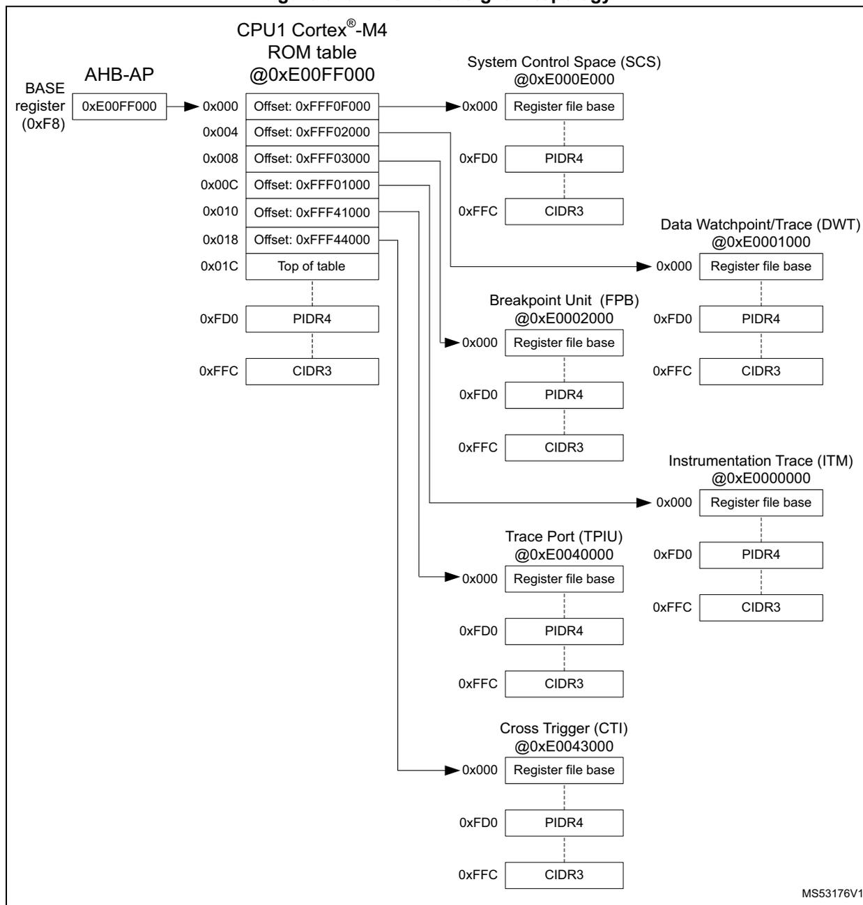
The diagram illustrates the CPU1 CoreSight™ topology. It shows the connection of various debug components to the CPU1 Cortex-M4 via an AHB-AP. The AHB-AP base register (0xF8) points to the ROM table at 0xE00FF000. The ROM table contains entries for the CPU1 Cortex-M4, System Control Space (SCS), Breakpoint Unit (FPB), Data Watchpoint/Trace (DWT), Instrumentation Trace (ITM), Trace Port (TPIU), and Cross Trigger (CTI). Each component has a register file base and specific registers like PIDR4 and CIDR3.
CPU1 Cortex®-M4 ROM table @0xE00FF000
- 0x000 Offset: 0xFFF0F000 → 0x000 Register file base
- 0x004 Offset: 0xFFF02000
- 0x008 Offset: 0xFFF03000 → 0xFD0 PIDR4
- 0x00C Offset: 0xFFF01000 → 0xFFC CIDR3
- 0x010 Offset: 0xFFF41000
- 0x018 Offset: 0xFFF44000
- 0x01C Top of table
System Control Space (SCS) @0xE000E000
- 0x000 Register file base
- 0xFD0 PIDR4
- 0xFFC CIDR3
Breakpoint Unit (FPB) @0xE0002000
- 0x000 Register file base
- 0xFD0 PIDR4
- 0xFFC CIDR3
Data Watchpoint/Trace (DWT) @0xE0001000
- 0x000 Register file base
- 0xFD0 PIDR4
- 0xFFC CIDR3
Instrumentation Trace (ITM) @0xE0000000
- 0x000 Register file base
- 0xFD0 PIDR4
- 0xFFC CIDR3
Trace Port (TPIU) @0xE0040000
- 0x000 Register file base
- 0xFD0 PIDR4
- 0xFFC CIDR3
Cross Trigger (CTI) @0xE0043000
- 0x000 Register file base
- 0xFD0 PIDR4
- 0xFFC CIDR3
MS53176V1
33.13.1 CPU1 ROM memory type register (C1ROM_MEMTYPE)
Address offset: 0xFCC
Reset value: 0x0000 0001
| 31 | 30 | 29 | 28 | 27 | 26 | 25 | 24 | 23 | 22 | 21 | 20 | 19 | 18 | 17 | 16 |
|---|---|---|---|---|---|---|---|---|---|---|---|---|---|---|---|
| Res. | Res. | Res. | Res. | Res. | Res. | Res. | Res. | Res. | Res. | Res. | Res. | Res. | Res. | Res. | Res. |
| 15 | 14 | 13 | 12 | 11 | 10 | 9 | 8 | 7 | 6 | 5 | 4 | 3 | 2 | 1 | 0 |
| Res. | Res. | Res. | Res. | Res. | Res. | Res. | Res. | Res. | Res. | Res. | Res. | Res. | Res. | Res. | SYSEMEN |
| r |
Bits 31:1 Reserved, must be kept at reset value.
Bit 0 SYSEMEN : System memory
0x1: System memory is present on this bus
33.13.2 CPU1 ROM CoreSight peripheral identity register 4 (C1ROM_PIDR4)
Address offset: 0xFD0
Reset value: 0x0000 0000
| 31 | 30 | 29 | 28 | 27 | 26 | 25 | 24 | 23 | 22 | 21 | 20 | 19 | 18 | 17 | 16 |
|---|---|---|---|---|---|---|---|---|---|---|---|---|---|---|---|
| Res. | Res. | Res. | Res. | Res. | Res. | Res. | Res. | Res. | Res. | Res. | Res. | Res. | Res. | Res. | Res. |
| 15 | 14 | 13 | 12 | 11 | 10 | 9 | 8 | 7 | 6 | 5 | 4 | 3 | 2 | 1 | 0 |
| Res. | Res. | Res. | Res. | Res. | Res. | Res. | Res. | 4KCOUNT[3:0] | JEP106CON[3:0] | ||||||
| r | r | r | r | r | r | r | r | ||||||||
Bits 31:8 Reserved, must be kept at reset value.
Bits 7:4 4KCOUNT[3:0] : register file size
0x0: Register file occupies a single 4 KB region
Bits 3:0 JEP106CON[3:0] : JEP106 continuation code
0x0: STMicroelectronics JEDEC continuation code
33.13.3 CPU1 ROM CoreSight peripheral identity register 0 (C1ROM_PIDR0)
Address offset: 0xFE0
Reset value: 0x0000 0094
| 31 | 30 | 29 | 28 | 27 | 26 | 25 | 24 | 23 | 22 | 21 | 20 | 19 | 18 | 17 | 16 |
|---|---|---|---|---|---|---|---|---|---|---|---|---|---|---|---|
| Res. | Res. | Res. | Res. | Res. | Res. | Res. | Res. | Res. | Res. | Res. | Res. | Res. | Res. | Res. | Res. |
| 15 | 14 | 13 | 12 | 11 | 10 | 9 | 8 | 7 | 6 | 5 | 4 | 3 | 2 | 1 | 0 |
| Res. | Res. | Res. | Res. | Res. | Res. | Res. | Res. | PARTNUM[7:0] | |||||||
| r | r | r | r | r | r | r | r | ||||||||
Bits 31:8 Reserved, must be kept at reset value.
Bits 7:0
PARTNUM[7:0]
: Part number bits [7:0]
0x94: STM32WB15CC
33.13.4 CPU1 ROM CoreSight peripheral identity register 1 (C1ROM_PIDR1)
Address offset: 0xFE4
Reset value: 0x0000 0004
| 31 | 30 | 29 | 28 | 27 | 26 | 25 | 24 | 23 | 22 | 21 | 20 | 19 | 18 | 17 | 16 |
|---|---|---|---|---|---|---|---|---|---|---|---|---|---|---|---|
| Res. | Res. | Res. | Res. | Res. | Res. | Res. | Res. | Res. | Res. | Res. | Res. | Res. | Res. | Res. | Res. |
| 15 | 14 | 13 | 12 | 11 | 10 | 9 | 8 | 7 | 6 | 5 | 4 | 3 | 2 | 1 | 0 |
| Res. | Res. | Res. | Res. | Res. | Res. | Res. | Res. | JEP106ID[3:0] | PARTNUM[11:8] | ||||||
| r | r | r | r | r | r | r | r | ||||||||
Bit 31:8 Reserved, must be kept at reset value.
Bits 7:4
JEP106ID[3:0]
: JEP106 identity code bits [3:0]
0x0: STMicroelectronics JEDEC code
Bits 3:0
PARTNUM[11:8]
: Part number bits [11:8]
0x4: STM32WB15CC
33.13.5 CPU1 ROM CoreSight peripheral identity register 2 (C1ROM_PIDR2)
Address offset: 0xFE8
Reset value: 0x0000 000A
| 31 | 30 | 29 | 28 | 27 | 26 | 25 | 24 | 23 | 22 | 21 | 20 | 19 | 18 | 17 | 16 |
|---|---|---|---|---|---|---|---|---|---|---|---|---|---|---|---|
| Res. | Res. | Res. | Res. | Res. | Res. | Res. | Res. | Res. | Res. | Res. | Res. | Res. | Res. | Res. | Res. |
| 15 | 14 | 13 | 12 | 11 | 10 | 9 | 8 | 7 | 6 | 5 | 4 | 3 | 2 | 1 | 0 |
| Res. | Res. | Res. | Res. | Res. | Res. | Res. | Res. | REVISION[3:0] | JEDEC | JEP106ID[6:4] | |||||
| r | r | r | r | r | r | r | r | ||||||||
Bit 31:8 Reserved, must be kept at reset value.
Bits 7:4
REVISION[3:0]
: Component revision number
0x0: rev r0p0
Bit 3
JEDEC
: JEDEC assigned value
0x1: Designer ID specified by JEDEC
Bits 2:0
JEP106ID[6:4]
: JEP106 identity code bits [6:4]
0x2: STMicroelectronics JEDEC code
33.13.6 CPU1 ROM CoreSight peripheral identity register 3 (C1ROM_PIDR3)
Address offset: 0xFEC
Reset value: 0x0000 0000
| 31 | 30 | 29 | 28 | 27 | 26 | 25 | 24 | 23 | 22 | 21 | 20 | 19 | 18 | 17 | 16 |
|---|---|---|---|---|---|---|---|---|---|---|---|---|---|---|---|
| Res. | Res. | Res. | Res. | Res. | Res. | Res. | Res. | Res. | Res. | Res. | Res. | Res. | Res. | Res. | Res. |
| 15 | 14 | 13 | 12 | 11 | 10 | 9 | 8 | 7 | 6 | 5 | 4 | 3 | 2 | 1 | 0 |
| Res. | Res. | Res. | Res. | Res. | Res. | Res. | Res. | REVAND[3:0] | CMOD[3:0] | ||||||
| r | r | r | r | r | r | r | r | ||||||||
Bit 31:8 Reserved, must be kept at reset value.
Bits 7:4 REVAND[3:0] : metal fix version
0x0: No metal fix
Bits 3:0 CMOD[3:0] : Customer modified
0x0: No customer modifications
33.13.7 CPU1 ROM CoreSight component identity register 0 (C1ROM_CIDR0)
Address offset: 0xFF0
Reset value: 0x0000 000D
| 31 | 30 | 29 | 28 | 27 | 26 | 25 | 24 | 23 | 22 | 21 | 20 | 19 | 18 | 17 | 16 |
|---|---|---|---|---|---|---|---|---|---|---|---|---|---|---|---|
| Res. | Res. | Res. | Res. | Res. | Res. | Res. | Res. | Res. | Res. | Res. | Res. | Res. | Res. | Res. | Res. |
| 15 | 14 | 13 | 12 | 11 | 10 | 9 | 8 | 7 | 6 | 5 | 4 | 3 | 2 | 1 | 0 |
| Res. | Res. | Res. | Res. | Res. | Res. | Res. | Res. | PREAMBLE[7:0] | |||||||
| r | r | r | r | r | r | r | r | ||||||||
Bits 31:8 Reserved, must be kept at reset value.
Bits 7:0 PREAMBLE[7:0] : Component ID bits [7:0]
0x0D: Common ID value
33.13.8 CPU1 ROM CoreSight peripheral identity register 1 (C1ROM_CIDR1)
Address offset: 0xFF4
Reset value: 0x0000 0010
| 31 | 30 | 29 | 28 | 27 | 26 | 25 | 24 | 23 | 22 | 21 | 20 | 19 | 18 | 17 | 16 |
|---|---|---|---|---|---|---|---|---|---|---|---|---|---|---|---|
| Res. | Res. | Res. | Res. | Res. | Res. | Res. | Res. | Res. | Res. | Res. | Res. | Res. | Res. | Res. | Res. |
| 15 | 14 | 13 | 12 | 11 | 10 | 9 | 8 | 7 | 6 | 5 | 4 | 3 | 2 | 1 | 0 |
| Res. | Res. | Res. | Res. | Res. | Res. | Res. | Res. | ||||||||
| r | r | r | r | r | r | r | r | ||||||||
| CLASS[3:0] | PREAMBLE[11:8] | ||||||||||||||
Bit 31:8 Reserved, must be kept at reset value.
Bits 7:4 CLASS[3:0] : Component ID bits [15:12] - component class
0x1: ROM table component
Bits 3:0 PREAMBLE[11:8] : Component ID bits [11:8]
0x0: Common ID value
33.13.9 CPU1 ROM CoreSight component identity register 2 (C1ROM_CIDR2)
Address offset: 0xFF8
Reset value: 0x0000 0005
| 31 | 30 | 29 | 28 | 27 | 26 | 25 | 24 | 23 | 22 | 21 | 20 | 19 | 18 | 17 | 16 |
|---|---|---|---|---|---|---|---|---|---|---|---|---|---|---|---|
| Res. | Res. | Res. | Res. | Res. | Res. | Res. | Res. | Res. | Res. | Res. | Res. | Res. | Res. | Res. | Res. |
| 15 | 14 | 13 | 12 | 11 | 10 | 9 | 8 | 7 | 6 | 5 | 4 | 3 | 2 | 1 | 0 |
| Res. | Res. | Res. | Res. | Res. | Res. | Res. | Res. | ||||||||
| r | r | r | r | r | r | r | r | ||||||||
| PREAMBLE[19:12] | |||||||||||||||
Bits 31:8 Reserved, must be kept at reset value.
Bits 7:0 PREAMBLE[19:12] : Component ID bits [23:16]
0x05: Common ID value
33.13.10 CPU1 ROM CoreSight component identity register 3 (C1ROM_CIDR3)
Address offset: 0xFFC
Reset value: 0x0000 00B1
| 31 | 30 | 29 | 28 | 27 | 26 | 25 | 24 | 23 | 22 | 21 | 20 | 19 | 18 | 17 | 16 |
|---|---|---|---|---|---|---|---|---|---|---|---|---|---|---|---|
| Res. | Res. | Res. | Res. | Res. | Res. | Res. | Res. | Res. | Res. | Res. | Res. | Res. | Res. | Res. | Res. |
| 15 | 14 | 13 | 12 | 11 | 10 | 9 | 8 | 7 | 6 | 5 | 4 | 3 | 2 | 1 | 0 |
| Res. | Res. | Res. | Res. | Res. | Res. | Res. | Res. | ||||||||
| r | r | r | r | r | r | r | r | ||||||||
| PREAMBLE[27:20] | |||||||||||||||
Bits 31:8 Reserved, must be kept at reset value.
Bits 7:0
PREAMBLE[27:20]
: Component ID bits [31:24]
0xB1: Common ID value
33.13.11 CPU1 ROM table register map and reset values
Table 227. CPU1 ROM table register map and reset values
| Offset | Register name | 31 | 30 | 29 | 28 | 27 | 26 | 25 | 24 | 23 | 22 | 21 | 20 | 19 | 18 | 17 | 16 | 15 | 14 | 13 | 12 | 11 | 10 | 9 | 8 | 7 | 6 | 5 | 4 | 3 | 2 | 1 | 0 |
|---|---|---|---|---|---|---|---|---|---|---|---|---|---|---|---|---|---|---|---|---|---|---|---|---|---|---|---|---|---|---|---|---|---|
| 0xFCC | C1ROM_MEMTYPE | Res. | Res. | Res. | Res. | Res. | Res. | Res. | Res. | Res. | Res. | Res. | Res. | Res. | Res. | Res. | Res. | Res. | Res. | Res. | Res. | Res. | Res. | Res. | Res. | Res. | Res. | Res. | Res. | Res. | Res. | Res. | SYSTEM |
| Reset value | 1 | ||||||||||||||||||||||||||||||||
| 0xFD0 | C1ROM_PIDR4 | Res. | Res. | Res. | Res. | Res. | Res. | Res. | Res. | Res. | Res. | Res. | Res. | Res. | Res. | Res. | Res. | Res. | Res. | Res. | Res. | Res. | Res. | Res. | Res. | Res. | 4KCOUNT | [3:0] | JEP106CON | [3:0] | |||
| Reset value | 0 | 0 | 0 | 0 | 0 | 0 | 0 | 0 | |||||||||||||||||||||||||
| 0xFE0 | C1ROM_PIDR0 | Res. | Res. | Res. | Res. | Res. | Res. | Res. | Res. | Res. | Res. | Res. | Res. | Res. | Res. | Res. | Res. | Res. | Res. | Res. | Res. | Res. | Res. | Res. | Res. | PARTNUM[7:0] | |||||||
| Reset value | 1 | 0 | 0 | 1 | 0 | 1 | 0 | 0 | |||||||||||||||||||||||||
| 0xFE4 | C1ROM_PIDR1 | Res. | Res. | Res. | Res. | Res. | Res. | Res. | Res. | Res. | Res. | Res. | Res. | Res. | Res. | Res. | Res. | Res. | Res. | Res. | Res. | Res. | Res. | Res. | Res. | JEP106ID | [3:0] | PARTNUM | [11:8] | ||||
| Reset value | 0 | 0 | 0 | 0 | 0 | 1 | 0 | 0 | |||||||||||||||||||||||||
| 0xFE8 | C1ROM_PIDR2 | Res. | Res. | Res. | Res. | Res. | Res. | Res. | Res. | Res. | Res. | Res. | Res. | Res. | Res. | Res. | Res. | Res. | Res. | Res. | Res. | Res. | Res. | Res. | Res. | REVISION | [3:0] | JEDEC | JEP106ID | [6:4] | |||
| Reset value | 0 | 0 | 0 | 0 | 1 | 0 | 1 | 0 | |||||||||||||||||||||||||
| 0xFEC | C1ROM_PIDR3 | Res. | Res. | Res. | Res. | Res. | Res. | Res. | Res. | Res. | Res. | Res. | Res. | Res. | Res. | Res. | Res. | Res. | Res. | Res. | Res. | Res. | Res. | Res. | Res. | REVAND[3:0] | CMOD[3:0] | ||||||
| Reset value | 0 | 0 | 0 | 0 | 0 | 0 | 0 | 0 | |||||||||||||||||||||||||
| 0xFF0 | C1ROM_CIDR0 | Res. | Res. | Res. | Res. | Res. | Res. | Res. | Res. | Res. | Res. | Res. | Res. | Res. | Res. | Res. | Res. | Res. | Res. | Res. | Res. | Res. | Res. | Res. | Res. | PREAMBLE[7:0] | |||||||
| Reset value | 0 | 0 | 0 | 0 | 1 | 1 | 0 | 1 | |||||||||||||||||||||||||
| 0xFF4 | C1ROM_CIDR1 | Res. | Res. | Res. | Res. | Res. | Res. | Res. | Res. | Res. | Res. | Res. | Res. | Res. | Res. | Res. | Res. | Res. | Res. | Res. | Res. | Res. | Res. | Res. | Res. | CLASS | [3:0] | PREAMBLE | [11:8] | ||||
| Reset value | 0 | 0 | 0 | 1 | 0 | 0 | 0 | 0 | |||||||||||||||||||||||||
| 0xFF8 | C1ROM_CIDR2 | Res. | Res. | Res. | Res. | Res. | Res. | Res. | Res. | Res. | Res. | Res. | Res. | Res. | Res. | Res. | Res. | Res. | Res. | Res. | Res. | Res. | Res. | Res. | Res. | PREAMBLE[19:12] | |||||||
| Reset value | 0 | 0 | 0 | 0 | 0 | 1 | 0 | 1 | |||||||||||||||||||||||||
| 0xFFC | C1ROM_CIDR3 | Res. | Res. | Res. | Res. | Res. | Res. | Res. | Res. | Res. | Res. | Res. | Res. | Res. | Res. | Res. | Res. | Res. | Res. | Res. | Res. | Res. | Res. | Res. | Res. | PREAMBLE[27:20] | |||||||
| Reset value | 1 | 0 | 1 | 1 | 0 | 0 | 0 | 1 | |||||||||||||||||||||||||
Refer to Section 33.13: CPU1 ROM table for the register boundary addresses.
33.14 CPU1 data watchpoint and trace unit (DWT)
The DWT provides four comparators that can be used as:
- • Watchpoint
- • ETM trigger
- • PC sampling trigger
- • Data address sampling trigger
- • Data comparator (comparator 1 only)
- • Clock cycle counter comparator (comparator 0 only)
It also contains counters for:
- • Clock cycles
- • Folded instructions
- • Load store unit (LSU) operations
- • Sleep cycles
- • Number of cycles per instruction
- • Interrupt overhead
A DWT comparator compares the value held in its DWT_COMP register with one of the following:
- • a data address
- • an instruction address
- • a data value
- • the cycle count value, for comparator 0 only.
For address matching, the comparator can use a mask, so it matches a range of addresses.
On a successful match, the comparator generates one of the following:
- • One or more DWT Data trace packets, containing one or more of:
- – the address of the instruction that caused a data access
- – an address offset, bits[15:0] of the data access address
- – the matched data value.
- • A watchpoint debug event, on either the PC value or the accessed data address.
- • A CMPMATCH[N] event, that signals the match outside the DWT unit.
A watchpoint debug event either generates a DebugMonitor exception, or causes the processor to halt execution and enter Debug state.
For more details on how to use the DWT, refer to the Arm ® v7-M Architecture Reference Manual [5].
33.14.1 DWT control register (DWT_CTRLR)
Address offset: 0x000
Reset value: 0x4000 0000
| 31 | 30 | 29 | 28 | 27 | 26 | 25 | 24 | 23 | 22 | 21 | 20 | 19 | 18 | 17 | 16 |
|---|---|---|---|---|---|---|---|---|---|---|---|---|---|---|---|
| NUMCOMP[3:0] | NOTR CPKT | NOEXT TRIG | NOCYC CNT | NOPRF CNT | Res. | CYCEV TENA | FOLDE VTENA | LSUEV TENA | SLEEPEVT ENA | EXCEVT ENA | CPIEV TENA | EXCTRC ENA | |||
| r | r | r | r | r | r | r | r | rw | rw | rw | rw | rw | rw | rw | |
| 15 | 14 | 13 | 12 | 11 | 10 | 9 | 8 | 7 | 6 | 5 | 4 | 3 | 2 | 1 | 0 |
| Res. | Res. | Res. | PCSAMPL ENA | SYNCTAP[1:0] | CYCTAP | POSTINIT[3:0] | POSTRESET[3:0] | CYCCNT ENA | |||||||
| rw | rw | rw | rw | rw | rw | rw | rw | rw | rw | rw | rw | rw | |||
Bits 31:28 NUMCOMP[3:0] : Number of comparators implemented (read only)
0x4: Four comparators
Bit 27 NOTRCPKT : Trace sampling and exception tracing support (read only)
0x0: Supported
Bit 26 NOEXTTRIG : External match signal, CMPMATCH support (read only)
0x0: Supported
Bit 25 NOCYCCNT : Cycle counter support (read only)
0x0: Supported
Bit 24 NOPRFCNT : Profiling counter support (read only)
0x0: Supported
Bit 23 Reserved, must be kept at reset value.
Bit 22 CYCEVTENA : Enable for POSTCNT underflow event counter packet generation
0x0: Disabled
0x1: Enabled
Bit 21 FOLDEVTENA : Enable for folded instruction counter overflow event generation
0x0: Disabled
0x1: Enabled
Bit 20 LSUEVTENA : Enable for LSU counter overflow event generation
0x0: Disabled
0x1: Enabled
Bit 19 SLEEPEVTENA : Enable for sleep counter overflow event generation
0x0: Disabled
0x1: Enabled
Bit 18 EXCEVTENA : Enable for exception overhead counter overflow event generation
0x0: Disabled
0x1: Enabled
Bit 17 CPIEVTENA : Enable for CPI counter overflow event generation
0x0: Disabled
0x1: Enabled
Bit 16 EXCTRCENA : Enable for exception trace generation
0x0: Disabled
0x1: Enabled
Bits 15:13 Reserved, must be kept at reset value.
- Bit 12
PCSAMPLENA
: Enables use of POSTCNT counter as a timer for Periodic PC sample packet generation.
- 0x0: Disabled
- 0x1: Enabled
- Bits 11:10
SYNCTAP[1:0]
: Selects the position of the synchronization packet counter tap on the CYCCNT counter. This determines the synchronization packet rate.
- 0x0: Disabled. No synchronization packets
- 0x1: Tap at CYCCNT[24]
- 0x2: Tap at CYCCNT[26]
- 0x3: Tap at CYCCNT[28]
- Bit 9
CYCTAP
: Selects the position of the POSTCNT tap on the CYCCNT counter.
- 0x0: Tap at CYCCNT[6]
- 0x1: Tap at CYCCNT[10]
- Bits 8:5 POSTINIT[3:0] : Initial value of the POSTCNT counter. Writes to this field are ignored if POSTCNT counter is enabled (ie. CYCEVTENA or PCSAMPLENA must be reset prior to writing POSTINIT).
- Bits 4:1 POSTPRESET[3:0] : Reload value of the POSTCNT counter.
- Bit 0
CYCCNTENA
: Enables CYCCNT counter.
- 0x0: Disabled
- 0x1: Enabled
33.14.2 DWT cycle count register (DWT_CYCCNTR)
Address offset: 0x004
Reset value: 0x0000 0000
| 31 | 30 | 29 | 28 | 27 | 26 | 25 | 24 | 23 | 22 | 21 | 20 | 19 | 18 | 17 | 16 |
| CYCCNT[31:16] | |||||||||||||||
| r | r | r | r | r | r | r | r | r | r | r | r | r | r | r | r |
| 15 | 14 | 13 | 12 | 11 | 10 | 9 | 8 | 7 | 6 | 5 | 4 | 3 | 2 | 1 | 0 |
| CYCCNT[15:0] | |||||||||||||||
| r | r | r | r | r | r | r | r | r | r | r | r | r | r | r | r |
Bits 31:0 CYCCNT[31:0] : Processor clock cycle counter
33.14.3 DWT CPI count register (DWT_CPICNTR)
Address offset: 0x008
Reset value: 0x0000 0000
| 31 | 30 | 29 | 28 | 27 | 26 | 25 | 24 | 23 | 22 | 21 | 20 | 19 | 18 | 17 | 16 |
|---|---|---|---|---|---|---|---|---|---|---|---|---|---|---|---|
| Res. | Res. | Res. | Res. | Res. | Res. | Res. | Res. | Res. | Res. | Res. | Res. | Res. | Res. | Res. | Res. |
| 15 | 14 | 13 | 12 | 11 | 10 | 9 | 8 | 7 | 6 | 5 | 4 | 3 | 2 | 1 | 0 |
| Res. | Res. | Res. | Res. | Res. | Res. | Res. | Res. | CPICNT[7:0] | |||||||
| rw | rw | rw | rw | rw | rw | rw | rw | ||||||||
Bits 31:8 Reserved, must be kept at reset value.
Bits 7:0 CPICNT[7:0] : CPI counter. Counts additional cycles required to execute multi-cycle instructions, except those recorded by DWT_LSUCNTR, and counts any instruction fetch stalls.
33.14.4 DWT exception count register (DWT_EXCCNTR)
Address offset: 0x00C
Reset value: 0x0000 0000
| 31 | 30 | 29 | 28 | 27 | 26 | 25 | 24 | 23 | 22 | 21 | 20 | 19 | 18 | 17 | 16 |
|---|---|---|---|---|---|---|---|---|---|---|---|---|---|---|---|
| Res. | Res. | Res. | Res. | Res. | Res. | Res. | Res. | Res. | Res. | Res. | Res. | Res. | Res. | Res. | Res. |
| 15 | 14 | 13 | 12 | 11 | 10 | 9 | 8 | 7 | 6 | 5 | 4 | 3 | 2 | 1 | 0 |
| Res. | Res. | Res. | Res. | Res. | Res. | Res. | Res. | EXCCNT[7:0] | |||||||
| rw | rw | rw | rw | rw | rw | rw | rw | ||||||||
Bits 31:8 Reserved, must be kept at reset value.
Bits 7:0 EXCCNT[7:0] : Exception overhead cycle counter. Counts the number of cycles spent in exception processing.
33.14.5 DWT sleep count register (DWT_SLP CNTR)
Address offset: 0x010
Reset value: 0x0000 0000
| 31 | 30 | 29 | 28 | 27 | 26 | 25 | 24 | 23 | 22 | 21 | 20 | 19 | 18 | 17 | 16 |
|---|---|---|---|---|---|---|---|---|---|---|---|---|---|---|---|
| Res. | Res. | Res. | Res. | Res. | Res. | Res. | Res. | Res. | Res. | Res. | Res. | Res. | Res. | Res. | Res. |
| 15 | 14 | 13 | 12 | 11 | 10 | 9 | 8 | 7 | 6 | 5 | 4 | 3 | 2 | 1 | 0 |
| Res. | Res. | Res. | Res. | Res. | Res. | Res. | Res. | SLEEP CNT[7:0] | |||||||
| rw | rw | rw | rw | rw | rw | rw | rw | ||||||||
Bits 31:8 Reserved, must be kept at reset value.
Bits 7:0 SLEEP CNT[7:0] : Sleep cycle counter. Counts the number of cycles spent in sleep mode (WFI, WFE, sleep-on-exit).
33.14.6 DWT LSU count register (DWT_LSUCNTR)
Address offset: 0x014
Reset value: 0x0000 0000
| 31 | 30 | 29 | 28 | 27 | 26 | 25 | 24 | 23 | 22 | 21 | 20 | 19 | 18 | 17 | 16 |
|---|---|---|---|---|---|---|---|---|---|---|---|---|---|---|---|
| Res. | Res. | Res. | Res. | Res. | Res. | Res. | Res. | Res. | Res. | Res. | Res. | Res. | Res. | Res. | Res. |
| 15 | 14 | 13 | 12 | 11 | 10 | 9 | 8 | 7 | 6 | 5 | 4 | 3 | 2 | 1 | 0 |
| Res. | Res. | Res. | Res. | Res. | Res. | Res. | Res. | LSUCNT[7:0] | |||||||
| rw | rw | rw | rw | rw | rw | rw | rw | ||||||||
Bits 31:8 Reserved, must be kept at reset value.
Bits 7:0 LSUCNT[7:0] : Load store counter. Counts additional cycles required to execute load and store instructions.
33.14.7 DWT fold count register (DWT_FOLDCNTR)
Address offset: 0x018
Reset value: 0x0000 0000
| 31 | 30 | 29 | 28 | 27 | 26 | 25 | 24 | 23 | 22 | 21 | 20 | 19 | 18 | 17 | 16 |
|---|---|---|---|---|---|---|---|---|---|---|---|---|---|---|---|
| Res. | Res. | Res. | Res. | Res. | Res. | Res. | Res. | Res. | Res. | Res. | Res. | Res. | Res. | Res. | Res. |
| 15 | 14 | 13 | 12 | 11 | 10 | 9 | 8 | 7 | 6 | 5 | 4 | 3 | 2 | 1 | 0 |
| Res. | Res. | Res. | Res. | Res. | Res. | Res. | Res. | FOLDCNT[7:0] | |||||||
| rw | rw | rw | rw | rw | rw | rw | rw | ||||||||
Bits 31:8 Reserved, must be kept at reset value.
Bits 7:0 FOLDCNT[7:0] : Folded instruction counter. Increments on each instruction that takes 0 cycles.
33.14.8 DWT program counter sample register (DWT_PCSR)
Address offset: 0x01C
Reset value: 0x0000 0000
| 31 | 30 | 29 | 28 | 27 | 26 | 25 | 24 | 23 | 22 | 21 | 20 | 19 | 18 | 17 | 16 |
|---|---|---|---|---|---|---|---|---|---|---|---|---|---|---|---|
| EIASAMPLE[31:16] | |||||||||||||||
| r | r | r | r | r | r | r | r | r | r | r | r | r | r | r | r |
| 15 | 14 | 13 | 12 | 11 | 10 | 9 | 8 | 7 | 6 | 5 | 4 | 3 | 2 | 1 | 0 |
| EIASAMPLE[15:0] | |||||||||||||||
| r | r | r | r | r | r | r | r | r | r | r | r | r | r | r | r |
Bits 31:0 EIASAMPLE[31:0] : Executed instruction address sample value. Samples the current value of the program counter.
33.14.9 DWT comparator register x (DWT_COMP x R)
Address offset: 0x020 + x * 0x10 (for x = 0 to 3)
Reset value: 0x0000 0000

| 31 | 30 | 29 | 28 | 27 | 26 | 25 | 24 | 23 | 22 | 21 | 20 | 19 | 18 | 17 | 16 |
| COMP[31:16] | |||||||||||||||
| r | r | r | r | r | r | r | r | r | r | r | r | r | r | r | r |
| 15 | 14 | 13 | 12 | 11 | 10 | 9 | 8 | 7 | 6 | 5 | 4 | 3 | 2 | 1 | 0 |
| COMP[15:0] | |||||||||||||||
| r | r | r | r | r | r | r | r | r | r | r | r | r | r | r | r |
Bits 31:0 COMP[31:0] : Reference value for comparison.
33.14.10 DWT mask register x (DWT_MASK x R)
Address offset: 0x024 + x * 0x10 (for x = 0 to 3)
Reset value: 0x0000 0000
| 31 | 30 | 29 | 28 | 27 | 26 | 25 | 24 | 23 | 22 | 21 | 20 | 19 | 18 | 17 | 16 |
| Res. | Res. | Res. | Res. | Res. | Res. | Res. | Res. | Res. | Res. | Res. | Res. | Res. | Res. | Res. | Res. |
| 15 | 14 | 13 | 12 | 11 | 10 | 9 | 8 | 7 | 6 | 5 | 4 | 3 | 2 | 1 | 0 |
| Res. | Res. | Res. | Res. | Res. | Res. | Res. | Res. | Res. | Res. | Res. | MASK[4:0] | ||||
| rw | rw | rw | rw | rw | |||||||||||
Bits 31:5 Reserved, must be kept at reset value.
Bits 4:0 MASK[4:0] : Comparator mask size. Provides the size of the ignore mask applied to the access address for address range matching by comparator n . A debugger can write 0b11111 to this field and then read the register back to determine the maximum mask size supported.
33.14.11 DWT function register x (DWT_FUNCT x R)
Address offset: 0x028 + x * 0x10 (for x = 0 to 3)
Reset value: 0x0000 0000
| 31 | 30 | 29 | 28 | 27 | 26 | 25 | 24 | 23 | 22 | 21 | 20 | 19 | 18 | 17 | 16 |
|---|---|---|---|---|---|---|---|---|---|---|---|---|---|---|---|
| Res. | Res. | Res. | Res. | Res. | Res. | Res. | Res. | Res. | Res. | Res. | Res. | DATAVADDR1[3:0] | |||
| rw | rw | rw | rw | ||||||||||||
| 15 | 14 | 13 | 12 | 11 | 10 | 9 | 8 | 7 | 6 | 5 | 4 | 3 | 2 | 1 | 0 |
| DATAVADDR0[3:0] | DATAVSIZE[1:0] | LINK1ENA | DATAVMATCH | CYCMATCH | Res. | EMITRANGE | Res. | FUNCTION[3:0] | |||||||
| rw | rw | rw | rw | rw | rw | rw | rw | rw | rw | rw | rw | rw | rw | ||
Bits 31:25 Reserved, must be kept at reset value.
Bit 24 MATCHED : Comparator match (read only). Indicates if a comparator match has occurred since the register was last read.
0: No match
1: Match occurred
Bits 23:20 Reserved, must be kept at reset value.
Bits 19:16 DATAVADDR1[3:0] : When the DATAVMATCH and LNK1ENA bits are both 1, this field can hold the comparator number of a second comparator to use for linked address comparison.
Bits 15:12 DATAVADDR0[3:0] : When the DATAVMATCH and LNK1ENA bits are both 1, this field can hold the comparator number of a comparator to use for linked address comparison.
Bits 11:10 DATAVSIZE[1:0] : For data value matching, specifies the size of the required data comparison.
0x0: Byte
0x1: Half word
0x2: Word
0x3: Reserved
Bit 9 LNK1ENA : Indicates whether use of a second linked comparator is supported (read only).
0x1: Supported
Bit 8 DATAVMATCH : Enables cycle comparison.
0x0: Perform address comparison
0x1: Perform data value comparison
Bit 7 CYCMATCH : Enables cycle count comparison on comparator 0. This field is reserved for other comparators.
0x0: No cycle count comparison
0x1: Compare DWT_COMP0R with the cycle counter, DWT_CYCCNTR
Bit 6 Reserved, must be kept at reset value.
Bit 5 EMITRANGE : Enables generation of data trace address offset packets (containing data address bits 0 to 15)
0x0: Disabled
0x1: Enabled
Bit 4 Reserved, must be kept at reset value.
Bits 3:0 FUNCTION[3:0] : Selects action to take on comparator match. The meaning of this bit field depends on the setting of the DATAVMATCH and CYCMATCH fields. See [5].
33.14.12 DWT CoreSight peripheral identity register 4 (DWT_PIDR4)
Address offset: 0xFD0
Reset value: 0x0000 0004
| 31 | 30 | 29 | 28 | 27 | 26 | 25 | 24 | 23 | 22 | 21 | 20 | 19 | 18 | 17 | 16 |
|---|---|---|---|---|---|---|---|---|---|---|---|---|---|---|---|
| Res. | Res. | Res. | Res. | Res. | Res. | Res. | Res. | Res. | Res. | Res. | Res. | Res. | Res. | Res. | Res. |
| 15 | 14 | 13 | 12 | 11 | 10 | 9 | 8 | 7 | 6 | 5 | 4 | 3 | 2 | 1 | 0 |
| Res. | Res. | Res. | Res. | Res. | Res. | Res. | Res. | 4KCOUNT[3:0] | JEP106CON[3:0] | ||||||
| r | r | r | r | r | r | r | r | ||||||||
Bits 31:8 Reserved, must be kept at reset value.
Bits 7:4 4KCOUNT[3:0] : register file size
0x0: Register file occupies a single 4 KB region
Bits 3:0 JEP106CON[3:0] : JEP106 continuation code
0x4: Arm® JEDEC code
33.14.13 DWT CoreSight peripheral identity register 0 (DWT_PIDR0)
Address offset: 0xFE0
Reset value: 0x0000 0002
| 31 | 30 | 29 | 28 | 27 | 26 | 25 | 24 | 23 | 22 | 21 | 20 | 19 | 18 | 17 | 16 |
|---|---|---|---|---|---|---|---|---|---|---|---|---|---|---|---|
| Res. | Res. | Res. | Res. | Res. | Res. | Res. | Res. | Res. | Res. | Res. | Res. | Res. | Res. | Res. | Res. |
| 15 | 14 | 13 | 12 | 11 | 10 | 9 | 8 | 7 | 6 | 5 | 4 | 3 | 2 | 1 | 0 |
| Res. | Res. | Res. | Res. | Res. | Res. | Res. | Res. | PARTNUM[7:0] | |||||||
| r | r | r | r | r | r | r | r | ||||||||
Bits 31:8 Reserved, must be kept at reset value.
Bits 7:0 PARTNUM[7:0] : Part number bits [7:0]
0x02: DWT part number
33.14.14 DWT CoreSight peripheral identity register 1 (DWT_PIDR1)
Address offset: 0xFE4
Reset value: 0x0000 00B9
| 31 | 30 | 29 | 28 | 27 | 26 | 25 | 24 | 23 | 22 | 21 | 20 | 19 | 18 | 17 | 16 |
|---|---|---|---|---|---|---|---|---|---|---|---|---|---|---|---|
| Res. | Res. | Res. | Res. | Res. | Res. | Res. | Res. | Res. | Res. | Res. | Res. | Res. | Res. | Res. | Res. |
| 15 | 14 | 13 | 12 | 11 | 10 | 9 | 8 | 7 | 6 | 5 | 4 | 3 | 2 | 1 | 0 |
| Res. | Res. | Res. | Res. | Res. | Res. | Res. | Res. | JEP106ID[3:0] | PARTNUM[11:8] | ||||||
| r | r | r | r | r | r | r | r | ||||||||
Bit 31:8 Reserved, must be kept at reset value.
Bits 7:4
JEP106ID[3:0]
: JEP106 identity code bits [3:0]
0xB: Arm® JEDEC code
Bits 3:0
PARTNUM[11:8]
: Part number bits [11:8]
0x9: DWT part number
33.14.15 DWT CoreSight peripheral identity register 2 (DWT_PIDR2)
Address offset: 0xFE8
Reset value: 0x0000 003B
| 31 | 30 | 29 | 28 | 27 | 26 | 25 | 24 | 23 | 22 | 21 | 20 | 19 | 18 | 17 | 16 |
|---|---|---|---|---|---|---|---|---|---|---|---|---|---|---|---|
| Res. | Res. | Res. | Res. | Res. | Res. | Res. | Res. | Res. | Res. | Res. | Res. | Res. | Res. | Res. | Res. |
| 15 | 14 | 13 | 12 | 11 | 10 | 9 | 8 | 7 | 6 | 5 | 4 | 3 | 2 | 1 | 0 |
| Res. | Res. | Res. | Res. | Res. | Res. | Res. | Res. | REVISION[3:0] | JEDEC | JEP106ID[6:4] | |||||
| r | r | r | r | r | r | r | r | ||||||||
Bit 31:8 Reserved, must be kept at reset value.
Bits 7:4
REVISION[3:0]
: Component revision number
0x3: r0p4
Bit 3
JEDEC
: JEDEC assigned value
0x1: Designer ID specified by JEDEC
Bits 2:0
JEP106ID[6:4]
: JEP106 identity code bits [6:4]
0x3: Arm® JEDEC code
33.14.16 DWT CoreSight peripheral identity register 3 (DWT_PIDR3)
Address offset: 0xFEC
Reset value: 0x0000 0000
| 31 | 30 | 29 | 28 | 27 | 26 | 25 | 24 | 23 | 22 | 21 | 20 | 19 | 18 | 17 | 16 |
|---|---|---|---|---|---|---|---|---|---|---|---|---|---|---|---|
| Res. | Res. | Res. | Res. | Res. | Res. | Res. | Res. | Res. | Res. | Res. | Res. | Res. | Res. | Res. | Res. |
| 15 | 14 | 13 | 12 | 11 | 10 | 9 | 8 | 7 | 6 | 5 | 4 | 3 | 2 | 1 | 0 |
| Res. | Res. | Res. | Res. | Res. | Res. | Res. | Res. | REVAND[3:0] | CMOD[3:0] | ||||||
| r | r | r | r | r | r | r | r | ||||||||
Bit 31:8 Reserved, must be kept at reset value.
Bits 7:4
REVAND[3:0]
: metal fix version
0x0: No metal fix
Bits 3:0
CMOD[3:0]
: Customer modified
0x0: No customer modifications
33.14.17 DWT CoreSight component identity register 0 (DWT_CIDR0)
Address offset: 0xFF0
Reset value: 0x0000 000D
| 31 | 30 | 29 | 28 | 27 | 26 | 25 | 24 | 23 | 22 | 21 | 20 | 19 | 18 | 17 | 16 |
|---|---|---|---|---|---|---|---|---|---|---|---|---|---|---|---|
| Res. | Res. | Res. | Res. | Res. | Res. | Res. | Res. | Res. | Res. | Res. | Res. | Res. | Res. | Res. | Res. |
| 15 | 14 | 13 | 12 | 11 | 10 | 9 | 8 | 7 | 6 | 5 | 4 | 3 | 2 | 1 | 0 |
| Res. | Res. | Res. | Res. | Res. | Res. | Res. | Res. | PREAMBLE[7:0] | |||||||
| r | r | r | r | r | r | r | r | ||||||||
Bits 31:8 Reserved, must be kept at reset value.
Bits 7:0 PREAMBLE[7:0] : Component ID bits [7:0]
0x0D: Common ID value
33.14.18 DWT CoreSight peripheral identity register 1 (DWT_PIDR1)
Address offset: 0xFF4
Reset value: 0x0000 00E0
| 31 | 30 | 29 | 28 | 27 | 26 | 25 | 24 | 23 | 22 | 21 | 20 | 19 | 18 | 17 | 16 |
|---|---|---|---|---|---|---|---|---|---|---|---|---|---|---|---|
| Res. | Res. | Res. | Res. | Res. | Res. | Res. | Res. | Res. | Res. | Res. | Res. | Res. | Res. | Res. | Res. |
| 15 | 14 | 13 | 12 | 11 | 10 | 9 | 8 | 7 | 6 | 5 | 4 | 3 | 2 | 1 | 0 |
| Res. | Res. | Res. | Res. | Res. | Res. | Res. | Res. | CLASS[3:0] | PREAMBLE[11:8] | ||||||
| r | r | r | r | r | r | r | r | ||||||||
Bit 31:8 Reserved, must be kept at reset value.
Bits 7:4 CLASS[3:0] : Component ID bits [15:12] - component class
0xE: Trace generator component
Bits 3:0 PREAMBLE[11:8] : Component ID bits [11:8]
0x0: Common ID value
33.14.19 DWT CoreSight component identity register 2 (DWT_CIDR2)
Address offset: 0xFF8
Reset value: 0x0000 0005
| 31 | 30 | 29 | 28 | 27 | 26 | 25 | 24 | 23 | 22 | 21 | 20 | 19 | 18 | 17 | 16 |
|---|---|---|---|---|---|---|---|---|---|---|---|---|---|---|---|
| Res. | Res. | Res. | Res. | Res. | Res. | Res. | Res. | Res. | Res. | Res. | Res. | Res. | Res. | Res. | Res. |
| 15 | 14 | 13 | 12 | 11 | 10 | 9 | 8 | 7 | 6 | 5 | 4 | 3 | 2 | 1 | 0 |
| Res. | Res. | Res. | Res. | Res. | Res. | Res. | Res. | PREAMBLE[19:12] | |||||||
| r | r | r | r | r | r | r | r | ||||||||
Bits 31:8 Reserved, must be kept at reset value.
Bits 7:0 PREAMBLE[19:12] : Component ID bits [23:16]
0x05: Common ID value
33.14.20 DWT CoreSight component identity register 3 (DWT_CIDR3)
Address offset: 0xFFC
Reset value: 0x0000 00B1
| 31 | 30 | 29 | 28 | 27 | 26 | 25 | 24 | 23 | 22 | 21 | 20 | 19 | 18 | 17 | 16 |
|---|---|---|---|---|---|---|---|---|---|---|---|---|---|---|---|
| Res. | Res. | Res. | Res. | Res. | Res. | Res. | Res. | Res. | Res. | Res. | Res. | Res. | Res. | Res. | Res. |
| 15 | 14 | 13 | 12 | 11 | 10 | 9 | 8 | 7 | 6 | 5 | 4 | 3 | 2 | 1 | 0 |
| Res. | Res. | Res. | Res. | Res. | Res. | Res. | Res. | PREAMBLE[27:20] | |||||||
| r | r | r | r | r | r | r | r | ||||||||
Bits 31:8 Reserved, must be kept at reset value.
Bits 7:0 PREAMBLE[27:20] : Component ID bits [31:24]
0xB1: Common ID value
33.14.21 CPU1 DWT register map and reset values
The CPU1 DWT registers are located at address range 0xE0001000 to 0xE0001FFC.
Table 228. CPU1 DWT register map and reset values
| Offset | Register name | 31 | 30 | 29 | 28 | 27 | 26 | 25 | 24 | 23 | 22 | 21 | 20 | 19 | 18 | 17 | 16 | 15 | 14 | 13 | 12 | 11 | 10 | 9 | 8 | 7 | 6 | 5 | 4 | 3 | 2 | 1 | 0 | |
|---|---|---|---|---|---|---|---|---|---|---|---|---|---|---|---|---|---|---|---|---|---|---|---|---|---|---|---|---|---|---|---|---|---|---|
| 0x000 | DWT_CTRLR | NUMCOMP [3:0] | NOTRCPKT | NOEXTTRIG | NOCYCCNT | NOPRFCNT | Res. | CYCEVTENA | FOLDEVTENA | LSUEVTENA | SLEEPEVTENA | EXCEVTENA | CPIEVTENA | EXCTRCENA | Res. | Res. | Res. | PCSAMPLENA | SYNCTAP [1:0] | CYCTAP | Res. | POSINIT[3:0] | POSTPRESET[3:0] | CYCCNTENA | ||||||||||
| Reset value | 0 | 1 | 0 | 0 | 0 | 0 | 0 | 0 | 0 | 0 | 0 | 0 | 0 | 0 | 0 | 0 | 0 | 0 | 0 | 0 | 0 | 0 | 0 | 0 | 0 | 0 | 0 | 0 | ||||||
| 0x004 | DWT_CYCCNTR | CYCCNT[31:0] | ||||||||||||||||||||||||||||||||
| Reset value | 0 | 0 | 0 | 0 | 0 | 0 | 0 | 0 | 0 | 0 | 0 | 0 | 0 | 0 | 0 | 0 | 0 | 0 | 0 | 0 | 0 | 0 | 0 | 0 | 0 | 0 | 0 | 0 | 0 | 0 | 0 | 0 | ||
| 0x008 | DWT_CPICNTR | Res. | CPICNT[7:0] | |||||||||||||||||||||||||||||||
| Reset value | 0 | 0 | 0 | 0 | 0 | 0 | 0 | 0 | ||||||||||||||||||||||||||
| 0x00C | DWT_EXCCNTR | Res. | EXCCNT[7:0] | |||||||||||||||||||||||||||||||
| Reset value | 0 | 0 | 0 | 0 | 0 | 0 | 0 | 0 | ||||||||||||||||||||||||||
| 0x010 | DWT_SLPCNTR | Res. | SLEEPCNT[7:0] | |||||||||||||||||||||||||||||||
| Reset value | 0 | 0 | 0 | 0 | 0 | 0 | 0 | 0 | ||||||||||||||||||||||||||
| 0x014 | DWT_LSUCNTR | Res. | LSUCNT[7:0] | |||||||||||||||||||||||||||||||
| Reset value | 0 | 0 | 0 | 0 | 0 | 0 | 0 | 0 | ||||||||||||||||||||||||||
| 0x018 | DWT_FOLDCNTR | Res. | FOLDCNT[7:0] | |||||||||||||||||||||||||||||||
| Reset value | 0 | 0 | 0 | 0 | 0 | 0 | 0 | 0 | ||||||||||||||||||||||||||
| 0x01C | DWT_PCSR | EIASAMPLE[31:0] | ||||||||||||||||||||||||||||||||
| Reset value | 0 | 0 | 0 | 0 | 0 | 0 | 0 | 0 | 0 | 0 | 0 | 0 | 0 | 0 | 0 | 0 | 0 | 0 | 0 | 0 | 0 | 0 | 0 | 0 | 0 | 0 | 0 | 0 | 0 | 0 | 0 | 0 | ||
| 0x020 | DWT_COMP0R | COMP[31:0] | ||||||||||||||||||||||||||||||||
| Reset value | 0 | 0 | 0 | 0 | 0 | 0 | 0 | 0 | 0 | 0 | 0 | 0 | 0 | 0 | 0 | 0 | 0 | 0 | 0 | 0 | 0 | 0 | 0 | 0 | 0 | 0 | 0 | 0 | 0 | 0 | 0 | 0 | ||
| 0x024 | DWT_MASK0R | Res. | MASK[4:0] | |||||||||||||||||||||||||||||||
| Reset value | 0 | 0 | 0 | 0 | 0 | |||||||||||||||||||||||||||||
| 0x028 | DWT_FUNCT0R | Res. | MATCHED | Res. | DATAVADDR1 [3:0] | DATAVADDR0 [3:0] | DATAVSIZE [1:0] | LNK1ENA | DATAVMATCH | CYCMATCH | Res. | EMITRANGE | Res. | FUNCTION [3:0] | ||||||||||||||||||||
| Reset value | 0 | 0 | 0 | 0 | 0 | 0 | 0 | 0 | 0 | 0 | 0 | 0 | 0 | 0 | 0 | 0 | 0 | 0 | 0 | 0 | 0 | 0 | ||||||||||||
| 0x030 | DWT_COMP1R | COMP[31:0] | ||||||||||||||||||||||||||||||||
| Reset value | 0 | 0 | 0 | 0 | 0 | 0 | 0 | 0 | 0 | 0 | 0 | 0 | 0 | 0 | 0 | 0 | 0 | 0 | 0 | 0 | 0 | 0 | 0 | 0 | 0 | 0 | 0 | 0 | 0 | 0 | 0 | 0 | ||
| 0x034 | DWT_MASK1R | Res. | MASK[4:0] | |||||||||||||||||||||||||||||||
| Reset value | 0 | 0 | 0 | 0 | 0 | |||||||||||||||||||||||||||||
| 0x038 | DWT_FUNCT1R | Res. | MATCHED | Res. | DATAVADDR1 [3:0] | DATAVADDR0 [3:0] | DATAVSIZE [1:0] | LNK1ENA | DATAVMATCH | CYCMATCH | Res. | EMITRANGE | Res. | FUNCTION [3:0] | ||||||||||||||||||||
| Reset value | 0 | 0 | 0 | 0 | 0 | 0 | 0 | 0 | 0 | 0 | 0 | 0 | 0 | 0 | 0 | 0 | 0 | 0 | 0 | 0 | 0 | 0 | ||||||||||||
Table 228. CPU1 DWT register map and reset values (continued)
| Offset | Register name | 31 | 30 | 29 | 28 | 27 | 26 | 25 | 24 | 23 | 22 | 21 | 20 | 19 | 18 | 17 | 16 | 15 | 14 | 13 | 12 | 11 | 10 | 9 | 8 | 7 | 6 | 5 | 4 | 3 | 2 | 1 | 0 |
|---|---|---|---|---|---|---|---|---|---|---|---|---|---|---|---|---|---|---|---|---|---|---|---|---|---|---|---|---|---|---|---|---|---|
| 0x040 | DWT_COMP2R | COMP[31:0] | |||||||||||||||||||||||||||||||
| Reset value | 0 | 0 | 0 | 0 | 0 | 0 | 0 | 0 | 0 | 0 | 0 | 0 | 0 | 0 | 0 | 0 | 0 | 0 | 0 | 0 | 0 | 0 | 0 | 0 | 0 | 0 | 0 | 0 | 0 | 0 | 0 | 0 | |
| 0x044 | DWT_MASK2R | Res. | Res. | Res. | Res. | Res. | Res. | Res. | Res. | Res. | Res. | Res. | Res. | Res. | Res. | Res. | Res. | Res. | Res. | Res. | Res. | Res. | Res. | Res. | Res. | Res. | Res. | Res. | Res. | Res. | Res. | Res. | MASK[4:0] |
| Reset value | 0 0 0 0 0 | ||||||||||||||||||||||||||||||||
| 0x048 | DWT_FUNCT2R | Res. | Res. | Res. | Res. | Res. | Res. | Res. | MATCHED | Res. | Res. | Res. | Res. | Res. | DATAVADDR1[3:0] | DATAVADDR0[3:0] | DATASIZE[1:0] | LNK1ENA | DATAMATCH | CYCMATCH | Res. | EMITRANGE | Res. | FUNCTION[3:0] | |||||||||
| Reset value | 0 | 0 | 0 | 0 | 0 | 0 | 0 | 0 | 0 | 0 | 0 | 0 | 0 | 0 | 0 | 0 | 0 | 0 0 0 0 | |||||||||||||||
| 0x050 | DWT_COMP3R | COMP[31:0] | |||||||||||||||||||||||||||||||
| Reset value | 0 | 0 | 0 | 0 | 0 | 0 | 0 | 0 | 0 | 0 | 0 | 0 | 0 | 0 | 0 | 0 | 0 | 0 | 0 | 0 | 0 | 0 | 0 | 0 | 0 | 0 | 0 | 0 | 0 | 0 | 0 | 0 | |
| 0x054 | DWT_MASK3R | Res. | Res. | Res. | Res. | Res. | Res. | Res. | Res. | Res. | Res. | Res. | Res. | Res. | Res. | Res. | Res. | Res. | Res. | Res. | Res. | Res. | Res. | Res. | Res. | Res. | Res. | Res. | Res. | Res. | Res. | Res. | MASK[4:0] |
| Reset value | 0 0 0 0 0 | ||||||||||||||||||||||||||||||||
| 0x058 | DWT_FUNCT3R | Res. | Res. | Res. | Res. | Res. | Res. | Res. | MATCHED | Res. | Res. | Res. | Res. | Res. | DATAVADDR1[3:0] | DATAVADDR0[3:0] | DATASIZE[1:0] | LNK1ENA | DATAMATCH | CYCMATCH | Res. | EMITRANGE | Res. | FUNCTION[3:0] | |||||||||
| Reset value | 0 | 0 | 0 | 0 | 0 | 0 | 0 | 0 | 0 | 0 | 0 | 0 | 0 | 0 | 0 | 0 | 0 | 0 0 0 0 | |||||||||||||||
| 0xFD0 | DWT_PIDR4 | Res. | Res. | Res. | Res. | Res. | Res. | Res. | Res. | Res. | Res. | Res. | Res. | Res. | Res. | Res. | Res. | Res. | Res. | Res. | Res. | Res. | Res. | Res. | Res. | Res. | Res. | 4KCOUNT[3:0] | JEP106CON[3:0] | ||||
| Reset value | 0 0 0 0 | 0 | 0 | 1 0 0 0 | |||||||||||||||||||||||||||||
| 0xFE0 | DWT_PIDR0 | Res. | Res. | Res. | Res. | Res. | Res. | Res. | Res. | Res. | Res. | Res. | Res. | Res. | Res. | Res. | Res. | Res. | Res. | Res. | Res. | Res. | Res. | Res. | Res. | Res. | Res. | Res. | Res. | Res. | Res. | Res. | PARTNUM[7:0] |
| Reset value | 0 0 0 0 0 0 1 0 | ||||||||||||||||||||||||||||||||
| 0xFE4 | DWT_PIDR1 | Res. | Res. | Res. | Res. | Res. | Res. | Res. | Res. | Res. | Res. | Res. | Res. | Res. | Res. | Res. | Res. | Res. | Res. | Res. | Res. | Res. | Res. | Res. | Res. | Res. | Res. | JEP106ID[3:0] | PARTNUM[11:8] | ||||
| Reset value | 1 0 1 1 | 0 | 0 | 0 0 0 0 | |||||||||||||||||||||||||||||
| 0xFE8 | DWT_PIDR2 | Res. | Res. | Res. | Res. | Res. | Res. | Res. | Res. | Res. | Res. | Res. | Res. | Res. | Res. | Res. | Res. | Res. | Res. | Res. | Res. | Res. | Res. | Res. | Res. | Res. | Res. | REVISION[3:0] | JEP106ID[6:4] | ||||
| Reset value | 0 0 1 1 | 1 | 1 0 1 1 | ||||||||||||||||||||||||||||||
| 0xFEC | DWT_PIDR3 | Res. | Res. | Res. | Res. | Res. | Res. | Res. | Res. | Res. | Res. | Res. | Res. | Res. | Res. | Res. | Res. | Res. | Res. | Res. | Res. | Res. | Res. | Res. | Res. | Res. | Res. | REVAND[3:0] | CMOD[3:0] | ||||
| Reset value | 0 0 0 0 | 0 | 0 0 0 0 | ||||||||||||||||||||||||||||||
| 0xFF0 | DWT_CIDR0 | Res. | Res. | Res. | Res. | Res. | Res. | Res. | Res. | Res. | Res. | Res. | Res. | Res. | Res. | Res. | Res. | Res. | Res. | Res. | Res. | Res. | Res. | Res. | Res. | Res. | Res. | Res. | Res. | Res. | Res. | PREAMBLE[7:0] | |
| Reset value | 0 0 0 0 1 1 0 1 | ||||||||||||||||||||||||||||||||
| 0xFF4 | DWT_CIDR1 | Res. | Res. | Res. | Res. | Res. | Res. | Res. | Res. | Res. | Res. | Res. | Res. | Res. | Res. | Res. | Res. | Res. | Res. | Res. | Res. | Res. | Res. | Res. | Res. | Res. | Res. | CLASS[3:0] | PREAMBLE[11:8] | ||||
| Reset value | 1 1 1 0 | 0 | 0 0 0 0 | ||||||||||||||||||||||||||||||
| 0xFF8 | DWT_CIDR2 | Res. | Res. | Res. | Res. | Res. | Res. | Res. | Res. | Res. | Res. | Res. | Res. | Res. | Res. | Res. | Res. | Res. | Res. | Res. | Res. | Res. | Res. | Res. | Res. | Res. | Res. | Res. | Res. | Res. | Res. | PREAMBLE[19:12] | |
| Reset value | 0 0 0 0 0 1 0 1 | ||||||||||||||||||||||||||||||||
| 0xFFC | DWT_CIDR3 | Res. | Res. | Res. | Res. | Res. | Res. | Res. | Res. | Res. | Res. | Res. | Res. | Res. | Res. | Res. | Res. | Res. | Res. | Res. | Res. | Res. | Res. | Res. | Res. | Res. | Res. | Res. | Res. | Res. | Res. | PREAMBLE[27:20] | |
| Reset value | 1 0 1 1 0 0 0 1 | ||||||||||||||||||||||||||||||||
Refer to Section 33.13: CPU1 ROM table for the register boundary addresses.
33.15 CPU1 instrumentation trace macrocell (ITM)
The ITM generates trace information as packets four sources can generate packets. If multiple sources generate packets at the same time, the ITM arbitrates the order in which packets are output. The four sources in decreasing order of priority are:
1. Software trace
Software can write directly to any of 32 x 32-bit ITM stimulus registers to generate packets. The permission level for each port can be programmed. When software writes to an enabled stimulus port, the ITM combines the identity of the port, the size of the write access and the data written, into a packet that it writes to a FIFO. The ITM outputs packets from the FIFO onto the trace bus. Reading a stimulus port register returns the status of the stimulus register (empty or pending) in bit 0.
2. Hardware trace
The DWT generates trace packets in response to a data trace event, a PC sample or a performance profiling counter wraparound. The ITM outputs these packets on the trace bus.
3. Local timestamping
The ITM contains a 21-bit counter clocked by the (pre-divided) processor clock. The counter value is output in a timestamp packet on the trace bus. The counter is reset to zero every time a timestamp packet is generated. The timestamps thus indicate the time elapsed since the previous timestamp packet.
33.15.1 ITM stimulus register x (ITM_STIMRx)
Address offset: 0x000 + x * 0x4 (x = 0 to 31)
Reset value: Unknown
| 31 | 30 | 29 | 28 | 27 | 26 | 25 | 24 | 23 | 22 | 21 | 20 | 19 | 18 | 17 | 16 |
| STIMULUS[31:16] | |||||||||||||||
| r | r | r | r | r | r | r | r | r | r | r | r | r | r | r | r |
| 15 | 14 | 13 | 12 | 11 | 10 | 9 | 8 | 7 | 6 | 5 | 4 | 3 | 2 | 1 | 0 |
| STIMULUS[15:0] | |||||||||||||||
| r | r | r | r | r | r | r | r | r | r | r | r | r | r | r | r |
Bits 31:0 STIMULUS[31:0] : Write data is output on the trace bus as a software event packet. When reading, bit 0 is a FIFOREADY indicator:
0: Stimulus port buffer is full (or port is disabled)
1: Stimulus port can accept new write data
33.15.2 ITM trace enable register (ITM_TER)
Address offset: 0x080
Reset value: 0x00000000
| 31 | 30 | 29 | 28 | 27 | 26 | 25 | 24 | 23 | 22 | 21 | 20 | 19 | 18 | 17 | 16 |
| STIMENA[31:16] | |||||||||||||||
| r | r | r | r | r | r | r | r | r | r | r | r | r | r | r | r |
| 15 | 14 | 13 | 12 | 11 | 10 | 9 | 8 | 7 | 6 | 5 | 4 | 3 | 2 | 1 | 0 |
| STIMENA[15:0] | |||||||||||||||
| r | r | r | r | r | r | r | r | r | r | r | r | r | r | r | r |
Bits 31:0 STIMENA[31:0] : Each bit n (0:31) enables the stimulus port associated with the ITM_STIMRn register.
0: Port disabled
1: Port enabled
33.15.3 ITM trace privilege register (ITM_TPR)
Address offset: 0xE00
Reset value: 0x00000000
| 31 | 30 | 29 | 28 | 27 | 26 | 25 | 24 | 23 | 22 | 21 | 20 | 19 | 18 | 17 | 16 |
| PRIVMASK[31:16] | |||||||||||||||
| r | r | r | r | r | r | r | r | r | r | r | r | r | r | r | r |
| 15 | 14 | 13 | 12 | 11 | 10 | 9 | 8 | 7 | 6 | 5 | 4 | 3 | 2 | 1 | 0 |
| PRIVSK[15:0] | |||||||||||||||
| r | r | r | r | r | r | r | r | r | r | r | r | r | r | r | r |
Bits 31:0 PRIVMASK[31:0] : Enable unprivileged access to ITM stimulus ports. Each bit controls eight stimulus ports.
0bXXX0: Unprivileged access permitted on ports 0 to 7
0bXXX1: Only privileged access permitted on ports 0 to 7
0bXX0X: Unprivileged access permitted on ports 8 to 15
0bXX1X: Only privileged access permitted on ports 8 to 15
0bX0XX: Unprivileged access permitted on ports 16 to 23
0bX1XX: Only privileged access permitted on ports 16 to 23
0b0XXX: Unprivileged access permitted on ports 24 to 31
0b1XXX: Only privileged access permitted on ports 24 to 31
33.15.4 ITM trace control register (ITM_TCR)
Address offset: 0xE80
Reset value: 0x0000 0000
| 31 | 30 | 29 | 28 | 27 | 26 | 25 | 24 | 23 | 22 | 21 | 20 | 19 | 18 | 17 | 16 |
|---|---|---|---|---|---|---|---|---|---|---|---|---|---|---|---|
| Res. | Res. | Res. | Res. | Res. | Res. | Res. | Res. | BUSY | TRACEBUSID[6:0] | ||||||
| rw | rw | rw | rw | rw | rw | rw | rw | ||||||||
| 15 | 14 | 13 | 12 | 11 | 10 | 9 | 8 | 7 | 6 | 5 | 4 | 3 | 2 | 1 | 0 |
| Res. | Res. | Res. | Res. | Res. | Res. | TSPRESCALE[1:0] | Res. | Res. | Res. | SWOENA | TXENA | SYNCENA | TSENA | ITMENA | |
| rw | rw | r | rw | rw | rw | rw | |||||||||
Bits 31:24 Reserved, must be kept at reset value.
Bit 23 BUSY : Indicates whether the ITM is currently processing events (read only).
0: Not busy
1: Busy
Bits 22:16 TRACEBUSID[6:0] : Identifier for multi-source trace stream formatting. If multi-source trace is in use, the debugger must write a non-zero value to this field. Note: different IDs must be used for each trace source in the system.
Bits 15:10 Reserved, must be kept at reset value.
Bits 9:8 TSPRESCALE[1:0] : Local timestamp prescaler, used with the trace packet reference clock. The possible values are:
0x0: No prescaling.
0x1: Divide by 4.
0x2: Divide by 16.
0x3: Divide by 64.
Bit 7:5 Reserved, must be kept at reset value.
Bit 4 SWOENA : Enables asynchronous clocking of the timestamp counter (read only).
0: Timestamp counter uses processor clock
Bit 3 TXENA : Enables forwarding of hardware event packets from the DWT unit to the trace port.
0: Disabled
1: Enabled
Bit 2 SYNCENA : Enables synchronization packet transmission.
Note: The debugger setting this bit must also configure the DWT_CTRLR register SYNCTAP field in the DWT for correct synchronization speed.
0: Disabled
1: Enabled
Bit 1 TSENA : Enables local timestamp generation.
0: Disabled
1: Enabled
Bit 0 ITMENA : Enables the ITM.
0: Disabled
1: Enabled
33.15.5 ITM CoreSight peripheral identity register 4 (ITM_PIDR4)
Address offset: 0xFD0
Reset value: 0x0000 0004
| 31 | 30 | 29 | 28 | 27 | 26 | 25 | 24 | 23 | 22 | 21 | 20 | 19 | 18 | 17 | 16 |
|---|---|---|---|---|---|---|---|---|---|---|---|---|---|---|---|
| Res. | Res. | Res. | Res. | Res. | Res. | Res. | Res. | Res. | Res. | Res. | Res. | Res. | Res. | Res. | Res. |
| 15 | 14 | 13 | 12 | 11 | 10 | 9 | 8 | 7 | 6 | 5 | 4 | 3 | 2 | 1 | 0 |
| Res. | Res. | Res. | Res. | Res. | Res. | Res. | Res. | 4KCOUNT[3:0] | JEP106CON[3:0] | ||||||
| r | r | r | r | r | r | r | r | ||||||||
Bits 31:8 Reserved, must be kept at reset value.
Bits 7:4 4KCOUNT[3:0] : register file size
0x0: Register file occupies a single 4 KB region
Bits 3:0 JEP106CON[3:0] : JEP106 continuation code
0x4: Arm ® JEDEC code
33.15.6 ITM CoreSight peripheral identity register 0 (ITM_PIDR0)
Address offset: 0xFE0
Reset value: 0x0000 0001
| 31 | 30 | 29 | 28 | 27 | 26 | 25 | 24 | 23 | 22 | 21 | 20 | 19 | 18 | 17 | 16 |
|---|---|---|---|---|---|---|---|---|---|---|---|---|---|---|---|
| Res. | Res. | Res. | Res. | Res. | Res. | Res. | Res. | Res. | Res. | Res. | Res. | Res. | Res. | Res. | Res. |
| 15 | 14 | 13 | 12 | 11 | 10 | 9 | 8 | 7 | 6 | 5 | 4 | 3 | 2 | 1 | 0 |
| Res. | Res. | Res. | Res. | Res. | Res. | Res. | Res. | PARTNUM[7:0] | |||||||
| r | r | r | r | r | r | r | r | ||||||||
Bits 31:8 Reserved, must be kept at reset value.
Bits 7:0 PARTNUM[7:0] : Part number bits [7:0]
0x01: ITM part number
33.15.7 ITM CoreSight peripheral identity register 1 (ITM_PIDR1)
Address offset: 0xFE4
Reset value: 0x0000 00B0
| 31 | 30 | 29 | 28 | 27 | 26 | 25 | 24 | 23 | 22 | 21 | 20 | 19 | 18 | 17 | 16 |
|---|---|---|---|---|---|---|---|---|---|---|---|---|---|---|---|
| Res. | Res. | Res. | Res. | Res. | Res. | Res. | Res. | Res. | Res. | Res. | Res. | Res. | Res. | Res. | Res. |
| 15 | 14 | 13 | 12 | 11 | 10 | 9 | 8 | 7 | 6 | 5 | 4 | 3 | 2 | 1 | 0 |
| Res. | Res. | Res. | Res. | Res. | Res. | Res. | Res. | JEP106ID[3:0] | PARTNUM[11:8] | ||||||
| r | r | r | r | r | r | r | r | ||||||||
Bit 31:8 Reserved, must be kept at reset value.
Bits 7:4 JEP106ID[3:0] : JEP106 identity code bits [3:0]
0xB: Arm® JEDEC code
Bits 3:0 PARTNUM[11:8] : Part number bits [11:8]
0x0: ITM part number
33.15.8 ITM CoreSight peripheral identity register 2 (ITM_PIDR2)
Address offset: 0xFE8
Reset value: 0x0000 003B
| 31 | 30 | 29 | 28 | 27 | 26 | 25 | 24 | 23 | 22 | 21 | 20 | 19 | 18 | 17 | 16 |
|---|---|---|---|---|---|---|---|---|---|---|---|---|---|---|---|
| Res. | Res. | Res. | Res. | Res. | Res. | Res. | Res. | Res. | Res. | Res. | Res. | Res. | Res. | Res. | Res. |
| 15 | 14 | 13 | 12 | 11 | 10 | 9 | 8 | 7 | 6 | 5 | 4 | 3 | 2 | 1 | 0 |
| Res. | Res. | Res. | Res. | Res. | Res. | Res. | Res. | REVISION[3:0] | JEDEC | JEP106ID[6:4] | |||||
| r | r | r | r | r | r | r | r | ||||||||
Bit 31:8 Reserved, must be kept at reset value.
Bits 7:4 REVISION[3:0] : Component revision number
0x3: r0p4
Bit 3 JEDEC : JEDEC assigned value
0x1: Designer ID specified by JEDEC
Bits 2:0 JEP106ID[6:4] : JEP106 identity code bits [6:4]
0x3: Arm® JEDEC code
33.15.9 ITM CoreSight peripheral identity register 3 (ITM_PIDR3)
Address offset: 0xFEC
Reset value: 0x0000 0000
| 31 | 30 | 29 | 28 | 27 | 26 | 25 | 24 | 23 | 22 | 21 | 20 | 19 | 18 | 17 | 16 |
|---|---|---|---|---|---|---|---|---|---|---|---|---|---|---|---|
| Res. | Res. | Res. | Res. | Res. | Res. | Res. | Res. | Res. | Res. | Res. | Res. | Res. | Res. | Res. | Res. |
| 15 | 14 | 13 | 12 | 11 | 10 | 9 | 8 | 7 | 6 | 5 | 4 | 3 | 2 | 1 | 0 |
| Res. | Res. | Res. | Res. | Res. | Res. | Res. | Res. | REVAND[3:0] | CMOD[3:0] | ||||||
| r | r | r | r | r | r | r | r | ||||||||
Bit 31:8 Reserved, must be kept at reset value.
Bits 7:4 REVAND[3:0] : metal fix version
0x0: No metal fix
Bits 3:0 CMOD[3:0] : Customer modified
0x0: No customer modifications
33.15.10 ITM CoreSight component identity register 0 (ITM_CIDR0)
Address offset: 0xFF0
Reset value: 0x0000 000D
| 31 | 30 | 29 | 28 | 27 | 26 | 25 | 24 | 23 | 22 | 21 | 20 | 19 | 18 | 17 | 16 |
|---|---|---|---|---|---|---|---|---|---|---|---|---|---|---|---|
| Res. | Res. | Res. | Res. | Res. | Res. | Res. | Res. | Res. | Res. | Res. | Res. | Res. | Res. | Res. | Res. |
| 15 | 14 | 13 | 12 | 11 | 10 | 9 | 8 | 7 | 6 | 5 | 4 | 3 | 2 | 1 | 0 |
| Res. | Res. | Res. | Res. | Res. | Res. | Res. | Res. | ||||||||
| PREAMBLE[7:0] | |||||||||||||||
| r | r | r | r | r | r | r | r | ||||||||
Bits 31:8 Reserved, must be kept at reset value.
Bits 7:0 PREAMBLE[7:0] : Component ID bits [7:0]
0x0D: Common ID value
33.15.11 ITM CoreSight peripheral identity register 1 (ITM_PIDR1)
Address offset: 0xFF4
Reset value: 0x0000 00E0
| 31 | 30 | 29 | 28 | 27 | 26 | 25 | 24 | 23 | 22 | 21 | 20 | 19 | 18 | 17 | 16 |
|---|---|---|---|---|---|---|---|---|---|---|---|---|---|---|---|
| Res. | Res. | Res. | Res. | Res. | Res. | Res. | Res. | Res. | Res. | Res. | Res. | Res. | Res. | Res. | Res. |
| 15 | 14 | 13 | 12 | 11 | 10 | 9 | 8 | 7 | 6 | 5 | 4 | 3 | 2 | 1 | 0 |
| Res. | Res. | Res. | Res. | Res. | Res. | Res. | Res. | ||||||||
| CLASS[3:0] | PREAMBLE[11:8] | ||||||||||||||
| r | r | r | r | r | r | r | r | ||||||||
Bit 31:8 Reserved, must be kept at reset value.
Bits 7:4 CLASS[3:0] : Component ID bits [15:12] - component class
0xE: Trace generator component
Bits 3:0 PREAMBLE[11:8] : Component ID bits [11:8]
0x0: Common ID value
33.15.12 ITM CoreSight component identity register 2 (ITM_CIDR2)
Address offset: 0xFF8
Reset value: 0x0000 0005
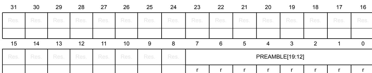
| 31 | 30 | 29 | 28 | 27 | 26 | 25 | 24 | 23 | 22 | 21 | 20 | 19 | 18 | 17 | 16 |
|---|---|---|---|---|---|---|---|---|---|---|---|---|---|---|---|
| Res. | Res. | Res. | Res. | Res. | Res. | Res. | Res. | Res. | Res. | Res. | Res. | Res. | Res. | Res. | Res. |
| 15 | 14 | 13 | 12 | 11 | 10 | 9 | 8 | 7 | 6 | 5 | 4 | 3 | 2 | 1 | 0 |
| Res. | Res. | Res. | Res. | Res. | Res. | Res. | Res. | PREAMBLE[19:12] | |||||||
| r | r | r | r | r | r | r | r | ||||||||
Bits 31:8 Reserved, must be kept at reset value.
Bits 7:0 PREAMBLE[19:12] : Component ID bits [23:16]
0x05: Common ID value
33.15.13 ITM CoreSight component identity register 3 (ITM_CIDR3)
Address offset: 0xFFC
Reset value: 0x0000 00B1

| 31 | 30 | 29 | 28 | 27 | 26 | 25 | 24 | 23 | 22 | 21 | 20 | 19 | 18 | 17 | 16 |
|---|---|---|---|---|---|---|---|---|---|---|---|---|---|---|---|
| Res. | Res. | Res. | Res. | Res. | Res. | Res. | Res. | Res. | Res. | Res. | Res. | Res. | Res. | Res. | Res. |
| 15 | 14 | 13 | 12 | 11 | 10 | 9 | 8 | 7 | 6 | 5 | 4 | 3 | 2 | 1 | 0 |
| Res. | Res. | Res. | Res. | Res. | Res. | Res. | Res. | PREAMBLE[27:20] | |||||||
| r | r | r | r | r | r | r | r | ||||||||
Bits 31:8 Reserved, must be kept at reset value.
Bits 7:0 PREAMBLE[27:20] : Component ID bits [31:24]
0xB1: Common ID value
33.15.14 ITM register map and reset values
The ITM registers are located at address range 0xE0000000 to 0xE0000FFC.
Table 229. CPU1 ITM register map and reset values
| Offset | Register name | 31 | 30 | 29 | 28 | 27 | 26 | 25 | 24 | 23 | 22 | 21 | 20 | 19 | 18 | 17 | 16 | 15 | 14 | 13 | 12 | 11 | 10 | 9 | 8 | 7 | 6 | 5 | 4 | 3 | 2 | 1 | 0 | |
|---|---|---|---|---|---|---|---|---|---|---|---|---|---|---|---|---|---|---|---|---|---|---|---|---|---|---|---|---|---|---|---|---|---|---|
| 0x000 to 0x07C | ITM_STIM0-31R | STIMULUS[31:0] | ||||||||||||||||||||||||||||||||
| Reset value | x | x | x | x | x | x | x | x | x | x | x | x | x | x | x | x | x | x | x | x | x | x | x | x | x | x | x | x | x | x | x | x | ||
| 0x0E00 | ITM_TER | STIMENA[31:0] | ||||||||||||||||||||||||||||||||
| Reset value | 0 | 0 | 0 | 0 | 0 | 0 | 0 | 0 | 0 | 0 | 0 | 0 | 0 | 0 | 0 | 0 | 0 | 0 | 0 | 0 | 0 | 0 | 0 | 0 | 0 | 0 | 0 | 0 | 0 | 0 | 0 | 0 | ||
| 0x0E40 | ITM_TPR | Res. | Res. | Res. | Res. | Res. | Res. | Res. | Res. | Res. | Res. | Res. | Res. | Res. | Res. | Res. | Res. | Res. | Res. | Res. | Res. | Res. | Res. | Res. | Res. | Res. | Res. | Res. | Res. | Res. | PRIVMASK[3:0] | |||
| Reset value | ||||||||||||||||||||||||||||||||||
| 0x0E80 | ITM_TCR | Res. | Res. | Res. | Res. | Res. | Res. | Res. | Res. | BUSY | TRACEBUSID[6:0] | Res. | Res. | Res. | GTSFREQ[1:0] | TSPRESCALE[1:0] | Res. | Res. | Res. | SWOENA | TXENA | SYNCENA | TSENA | ITMENA | ||||||||||
| Reset value | 0 | 0 | 0 | 0 | 0 | |||||||||||||||||||||||||||||
| 0xFD0 | ITM_PIDR4 | Res. | Res. | Res. | Res. | Res. | Res. | Res. | Res. | Res. | Res. | Res. | Res. | Res. | Res. | Res. | Res. | Res. | Res. | Res. | Res. | Res. | Res. | Res. | 4KCOUNT [3:0] | JEP106CON [3:0] | ||||||||
| Reset value | ||||||||||||||||||||||||||||||||||
| 0xFE0 | ITM_PIDR0 | Res. | Res. | Res. | Res. | Res. | Res. | Res. | Res. | Res. | Res. | Res. | Res. | Res. | Res. | Res. | Res. | Res. | Res. | Res. | Res. | Res. | Res. | Res. | PARTNUM[7:0] | |||||||||
| Reset value | ||||||||||||||||||||||||||||||||||
| 0xFE4 | ITM_PIDR1 | Res. | Res. | Res. | Res. | Res. | Res. | Res. | Res. | Res. | Res. | Res. | Res. | Res. | Res. | Res. | Res. | Res. | Res. | Res. | Res. | Res. | Res. | Res. | JEP106ID [3:0] | PARTNUM [11:8] | ||||||||
| Reset value | ||||||||||||||||||||||||||||||||||
| 0xFE8 | ITM_PIDR2 | Res. | Res. | Res. | Res. | Res. | Res. | Res. | Res. | Res. | Res. | Res. | Res. | Res. | Res. | Res. | Res. | Res. | Res. | Res. | Res. | Res. | Res. | Res. | REVISION [3:0] | JEDEC | JEP106ID [6:4] | |||||||
| Reset value | ||||||||||||||||||||||||||||||||||
| 0xFEC | ITM_PIDR3 | Res. | Res. | Res. | Res. | Res. | Res. | Res. | Res. | Res. | Res. | Res. | Res. | Res. | Res. | Res. | Res. | Res. | Res. | Res. | Res. | Res. | Res. | Res. | REVAND[3:0] | CMOD[3:0] | ||||||||
| Reset value | ||||||||||||||||||||||||||||||||||
| 0xFF0 | ITM_CIDR0 | Res. | Res. | Res. | Res. | Res. | Res. | Res. | Res. | Res. | Res. | Res. | Res. | Res. | Res. | Res. | Res. | Res. | Res. | Res. | Res. | Res. | Res. | Res. | PREAMBLE[7:0] | |||||||||
| Reset value | ||||||||||||||||||||||||||||||||||
| 0xFF4 | ITM_CIDR1 | Res. | Res. | Res. | Res. | Res. | Res. | Res. | Res. | Res. | Res. | Res. | Res. | Res. | Res. | Res. | Res. | Res. | Res. | Res. | Res. | Res. | Res. | Res. | CLASS[3:0] | PREAMBLE [11:8] | ||||||||
| Reset value | ||||||||||||||||||||||||||||||||||
| 0xFF8 | ITM_CIDR2 | Res. | Res. | Res. | Res. | Res. | Res. | Res. | Res. | Res. | Res. | Res. | Res. | Res. | Res. | Res. | Res. | Res. | Res. | Res. | Res. | Res. | Res. | Res. | PREAMBLE[19:12] | |||||||||
| Reset value | ||||||||||||||||||||||||||||||||||
| 0xFFC | ITM_CIDR3 | Res. | Res. | Res. | Res. | Res. | Res. | Res. | Res. | Res. | Res. | Res. | Res. | Res. | Res. | Res. | Res. | Res. | Res. | Res. | Res. | Res. | Res. | Res. | PREAMBLE[27:20] | |||||||||
| Reset value | ||||||||||||||||||||||||||||||||||
Refer to Section 33.13: CPU1 ROM table for the register boundary addresses.
33.16 CPU1 breakpoint unit (FPB)
The FPB allows the user to set hardware breakpoints. It contains six comparators that monitor the instruction fetch address and two literal address comparators. If a match occurs, the address is remapped to an address in system memory, defined by the FPB_REMAPR register plus an offset corresponding to the matching comparator. Alternatively, the instruction comparators can be configured to generate a breakpoint instruction.
33.16.1 FPB control register (FPB_CTRLR)
Address offset: 0x000
Reset value: 0x0000 0260
| 31 | 30 | 29 | 28 | 27 | 26 | 25 | 24 | 23 | 22 | 21 | 20 | 19 | 18 | 17 | 16 |
|---|---|---|---|---|---|---|---|---|---|---|---|---|---|---|---|
| Res. | Res. | Res. | Res. | Res. | Res. | Res. | Res. | Res. | Res. | Res. | Res. | Res. | Res. | Res. | Res. |
| 15 | 14 | 13 | 12 | 11 | 10 | 9 | 8 | 7 | 6 | 5 | 4 | 3 | 2 | 1 | 0 |
| Res. | NUM_CODE[6:4] | NUM_LIT[3:0] | NUM_CODE[3:0] | Res. | Res. | KEY | ENABLE | ||||||||
| r | r | r | r | r | r | r | r | r | r | r | rw | rw | |||
Bits 31:15 Reserved, must be kept at reset value.
Bits 14:12 NUM_CODE[6:4] : Number of instruction address comparators supported - least significant bits (read only).
0x0: 6 instruction comparators supported.
Bits 11:8 NUM_LIT[3:0] : Number of literal address comparators supported (read only).
0x2: Two literal comparators supported.
Bits 7:4 NUM_CODE[3:0] : Number of instruction address comparators supported - least significant bits (read only).
0x6: 6 instruction comparators supported
Bit 1 KEY : Write protect key. A write to FPB_CTRLR register is ignored if this bit is not set to 1.
Bits 0 ENABLE : FPB enable
0x0: Disable
0x1: Enable
33.16.2 FPB remap register (FPB_REMAPR)
Address offset: 0x004
Reset value: 0x2000 0000
| 31 | 30 | 29 | 28 | 27 | 26 | 25 | 24 | 23 | 22 | 21 | 20 | 19 | 18 | 17 | 16 |
|---|---|---|---|---|---|---|---|---|---|---|---|---|---|---|---|
| Res. | Res. | RMPSPRT | REMAP[23:11] | ||||||||||||
| r | rw | rw | rw | rw | rw | rw | rw | rw | rw | rw | rw | rw | rw | ||
| 15 | 14 | 13 | 12 | 11 | 10 | 9 | 8 | 7 | 6 | 5 | 4 | 3 | 2 | 1 | 0 |
| REMAP[10:0] | Res. | Res. | Res. | Res. | Res. | ||||||||||
| rw | rw | rw | rw | rw | rw | rw | rw | rw | rw | rw | |||||
Bits 31:30 Reserved, must be kept at reset value.
Bit 29
RMPSP
: Indicates whether Flash memory patch remap is supported (read only).
0x1: Remapping supported.
Bits 28:5 REMAP[23:0] : Remap target address. Bits [28:5] of the base address in SRAM to which the FPB remaps the address. The remap base address must be aligned to the number of words required to support the implemented comparators, that is to (NUM_CODE+NUM_LIT) words, with a minimum alignment of 8 words. Because remap is into the SRAM memory region, 0x20000000-0x3FFFFFF, bits [31:29] of the remap address are 0b001.
Bits 4:0 Reserved, must be kept at reset value.
33.16.3 FPB comparator registers (FPB_COMPxR)
Address offset: 0x008 + x * 0x4 (for x = 0 to 7)
Reset value: 0x0000 0000
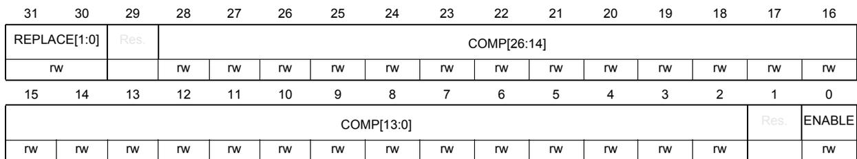
| 31 | 30 | 29 | 28 | 27 | 26 | 25 | 24 | 23 | 22 | 21 | 20 | 19 | 18 | 17 | 16 |
| REPLACE[1:0] | Res. | COMP[26:14] | |||||||||||||
| rw | rw | rw | rw | rw | rw | rw | rw | rw | rw | rw | rw | rw | rw | rw | |
| 15 | 14 | 13 | 12 | 11 | 10 | 9 | 8 | 7 | 6 | 5 | 4 | 3 | 2 | 1 | 0 |
| COMP[13:0] | Res. | ENABLE | |||||||||||||
| rw | rw | rw | rw | rw | rw | rw | rw | rw | rw | rw | rw | rw | rw | rw | |
Bits 31:30 REPLACE[1:0] : Defines the behavior when a match occurs between the COMP field and the instruction fetch address.
0x0: Reserved
0x1: Breakpoint on lower half-word, upper half-word is unaffected.
0x2: Breakpoint on upper half-word, lower half-word is unaffected.
0x3: Breakpoint on both upper and lower half-words.
Bit 29 Reserved, must be kept at reset value.
Bits 28:2 COMP[26:0] : Value to compare with address bits 28:2 of accesses to instruction code memory (0x00000000 to 0x1FFFFFF). If a match occurs, the action to be taken is defined by the REPLACE field.
Bit 1 Reserved, must be kept at reset value.
Bit 0 ENABLE : Comparator enable. The comparator is only enabled if both this bit and the FPB_ENABLE bit in the FPB_CTRLR register are set.
0: Disabled
1: Enabled
33.16.4 FPB CoreSight peripheral identity register 4 (FPB_PIDR4)
Address offset: 0xFD0
Reset value: 0x0000 0004
| 31 | 30 | 29 | 28 | 27 | 26 | 25 | 24 | 23 | 22 | 21 | 20 | 19 | 18 | 17 | 16 |
|---|---|---|---|---|---|---|---|---|---|---|---|---|---|---|---|
| Res. | Res. | Res. | Res. | Res. | Res. | Res. | Res. | Res. | Res. | Res. | Res. | Res. | Res. | Res. | Res. |
| 15 | 14 | 13 | 12 | 11 | 10 | 9 | 8 | 7 | 6 | 5 | 4 | 3 | 2 | 1 | 0 |
| Res. | Res. | Res. | Res. | Res. | Res. | Res. | Res. | 4KCOUNT[3:0] | JEP106CON[3:0] | ||||||
| r | r | r | r | r | r | r | r | ||||||||
Bits 31:8 Reserved, must be kept at reset value.
Bits 7:4 4KCOUNT[3:0] : register file size
0x0: Register file occupies a single 4 KB region
Bits 3:0 JEP106CON[3:0] : JEP106 continuation code
0x4: Arm® JEDEC code
33.16.5 FPB CoreSight peripheral identity register 0 (FPB_PIDR0)
Address offset: 0xFE0
Reset value: 0x0000 0003
| 31 | 30 | 29 | 28 | 27 | 26 | 25 | 24 | 23 | 22 | 21 | 20 | 19 | 18 | 17 | 16 |
|---|---|---|---|---|---|---|---|---|---|---|---|---|---|---|---|
| Res. | Res. | Res. | Res. | Res. | Res. | Res. | Res. | Res. | Res. | Res. | Res. | Res. | Res. | Res. | Res. |
| 15 | 14 | 13 | 12 | 11 | 10 | 9 | 8 | 7 | 6 | 5 | 4 | 3 | 2 | 1 | 0 |
| Res. | Res. | Res. | Res. | Res. | Res. | Res. | Res. | PARTNUM[7:0] | |||||||
| r | r | r | r | r | r | r | r | ||||||||
Bits 31:8 Reserved, must be kept at reset value.
Bits 7:0 PARTNUM[7:0] : Part number bits [7:0]
0x03: FPB part number
33.16.6 FPB CoreSight peripheral identity register 1 (FPB_PIDR1)
Address offset: 0xFE4
Reset value: 0x0000 00B0
| 31 | 30 | 29 | 28 | 27 | 26 | 25 | 24 | 23 | 22 | 21 | 20 | 19 | 18 | 17 | 16 |
|---|---|---|---|---|---|---|---|---|---|---|---|---|---|---|---|
| Res. | Res. | Res. | Res. | Res. | Res. | Res. | Res. | Res. | Res. | Res. | Res. | Res. | Res. | Res. | Res. |
| 15 | 14 | 13 | 12 | 11 | 10 | 9 | 8 | 7 | 6 | 5 | 4 | 3 | 2 | 1 | 0 |
| Res. | Res. | Res. | Res. | Res. | Res. | Res. | Res. | JEP106ID[3:0] | PARTNUM[11:8] | ||||||
| r | r | r | r | r | r | r | r | ||||||||
Bit 31:8 Reserved, must be kept at reset value.
Bits 7:4
JEP106ID[3:0]
: JEP106 identity code bits [3:0]
0xB: Arm® JEDEC code
Bits 3:0
PARTNUM[11:8]
: Part number bits [11:8]
0x0: FPB part number
33.16.7 FPB CoreSight peripheral identity register 2 (FPB_PIDR2)
Address offset: 0xFE8
Reset value: 0x0000 002B
| 31 | 30 | 29 | 28 | 27 | 26 | 25 | 24 | 23 | 22 | 21 | 20 | 19 | 18 | 17 | 16 |
|---|---|---|---|---|---|---|---|---|---|---|---|---|---|---|---|
| Res. | Res. | Res. | Res. | Res. | Res. | Res. | Res. | Res. | Res. | Res. | Res. | Res. | Res. | Res. | Res. |
| 15 | 14 | 13 | 12 | 11 | 10 | 9 | 8 | 7 | 6 | 5 | 4 | 3 | 2 | 1 | 0 |
| Res. | Res. | Res. | Res. | Res. | Res. | Res. | Res. | REVISION[3:0] | JEDEC | JEP106ID[6:4] | |||||
| r | r | r | r | r | r | r | r | ||||||||
Bit 31:8 Reserved, must be kept at reset value.
Bits 7:4
REVISION[3:0]
: Component revision number
0x2: r0p3
Bit 3
JEDEC
: JEDEC assigned value
0x1: Designer ID specified by JEDEC
Bits 2:0
JEP106ID[6:4]
: JEP106 identity code bits [6:4]
0x3: Arm® JEDEC code
33.16.8 FPB CoreSight peripheral identity register 3 (FPB_PIDR3)
Address offset: 0xFEC
Reset value: 0x0000 0000
| 31 | 30 | 29 | 28 | 27 | 26 | 25 | 24 | 23 | 22 | 21 | 20 | 19 | 18 | 17 | 16 |
|---|---|---|---|---|---|---|---|---|---|---|---|---|---|---|---|
| Res. | Res. | Res. | Res. | Res. | Res. | Res. | Res. | Res. | Res. | Res. | Res. | Res. | Res. | Res. | Res. |
| 15 | 14 | 13 | 12 | 11 | 10 | 9 | 8 | 7 | 6 | 5 | 4 | 3 | 2 | 1 | 0 |
| Res. | Res. | Res. | Res. | Res. | Res. | Res. | Res. | REVAND[3:0] | CMOD[3:0] | ||||||
| r | r | r | r | r | r | r | r | ||||||||
Bit 31:8 Reserved, must be kept at reset value.
Bits 7:4
REVAND[3:0]
: metal fix version
0x0: No metal fix
Bits 3:0
CMOD[3:0]
: Customer modified
0x0: No customer modifications
33.16.9 FPB CoreSight component identity register 0 (FPB_CIDR0)
Address offset: 0xFF0
Reset value: 0x0000 000D
| 31 | 30 | 29 | 28 | 27 | 26 | 25 | 24 | 23 | 22 | 21 | 20 | 19 | 18 | 17 | 16 |
|---|---|---|---|---|---|---|---|---|---|---|---|---|---|---|---|
| Res. | Res. | Res. | Res. | Res. | Res. | Res. | Res. | Res. | Res. | Res. | Res. | Res. | Res. | Res. | Res. |
| 15 | 14 | 13 | 12 | 11 | 10 | 9 | 8 | 7 | 6 | 5 | 4 | 3 | 2 | 1 | 0 |
| Res. | Res. | Res. | Res. | Res. | Res. | Res. | Res. | PREAMBLE[7:0] | |||||||
| r | r | r | r | r | r | r | r | ||||||||
Bits 31:8 Reserved, must be kept at reset value.
Bits 7:0 PREAMBLE[7:0] : Component ID bits [7:0]
0x0D: Common ID value
33.16.10 FPB CoreSight peripheral identity register 1 (FPB_CIDR1)
Address offset: 0xFF4
Reset value: 0x0000 00E0
| 31 | 30 | 29 | 28 | 27 | 26 | 25 | 24 | 23 | 22 | 21 | 20 | 19 | 18 | 17 | 16 |
|---|---|---|---|---|---|---|---|---|---|---|---|---|---|---|---|
| Res. | Res. | Res. | Res. | Res. | Res. | Res. | Res. | Res. | Res. | Res. | Res. | Res. | Res. | Res. | Res. |
| 15 | 14 | 13 | 12 | 11 | 10 | 9 | 8 | 7 | 6 | 5 | 4 | 3 | 2 | 1 | 0 |
| Res. | Res. | Res. | Res. | Res. | Res. | Res. | Res. | CLASS[3:0] | PREAMBLE[11:8] | ||||||
| r | r | r | r | r | r | r | r | ||||||||
Bit 31:8 Reserved, must be kept at reset value.
Bits 7:4 CLASS[3:0] : Component ID bits [15:12] - component class
0xE: Trace generator component
Bits 3:0 PREAMBLE[11:8] : Component ID bits [11:8]
0x0: Common ID value
33.16.11 FPB CoreSight component identity register 2 (FPB_CIDR2)
Address offset: 0xFF8
Reset value: 0x0000 0005
| 31 | 30 | 29 | 28 | 27 | 26 | 25 | 24 | 23 | 22 | 21 | 20 | 19 | 18 | 17 | 16 |
|---|---|---|---|---|---|---|---|---|---|---|---|---|---|---|---|
| Res. | Res. | Res. | Res. | Res. | Res. | Res. | Res. | Res. | Res. | Res. | Res. | Res. | Res. | Res. | Res. |
| 15 | 14 | 13 | 12 | 11 | 10 | 9 | 8 | 7 | 6 | 5 | 4 | 3 | 2 | 1 | 0 |
| Res. | Res. | Res. | Res. | Res. | Res. | Res. | Res. | PREAMBLE[19:12] | |||||||
| r | r | r | r | r | r | r | r | ||||||||
Bits 31:8 Reserved, must be kept at reset value.
Bits 7:0 PREAMBLE[19:12] : Component ID bits [23:16]
0x05: Common ID value
33.16.12 FPB CoreSight component identity register 3 (FPB_CIDR3)
Address offset: 0xFFC
Reset value: 0x0000 00B1
| 31 | 30 | 29 | 28 | 27 | 26 | 25 | 24 | 23 | 22 | 21 | 20 | 19 | 18 | 17 | 16 |
|---|---|---|---|---|---|---|---|---|---|---|---|---|---|---|---|
| Res. | Res. | Res. | Res. | Res. | Res. | Res. | Res. | Res. | Res. | Res. | Res. | Res. | Res. | Res. | Res. |
| 15 | 14 | 13 | 12 | 11 | 10 | 9 | 8 | 7 | 6 | 5 | 4 | 3 | 2 | 1 | 0 |
| Res. | Res. | Res. | Res. | Res. | Res. | Res. | Res. | PREAMBLE[27:20] | |||||||
| r | r | r | r | r | r | r | r | ||||||||
Bits 31:8 Reserved, must be kept at reset value.
Bits 7:0 PREAMBLE[27:20] : Component ID bits [31:24]
0xB1: Common ID value
33.16.13 FPB register map and reset values
The CPU1 FPB registers are located at address range 0xE0002000 to 0xE0002FFC.
Table 230. CPU1 FPB register map and reset values
| Offset | Register name | 31 | 30 | 29 | 28 | 27 | 26 | 25 | 24 | 23 | 22 | 21 | 20 | 19 | 18 | 17 | 16 | 15 | 14 | 13 | 12 | 11 | 10 | 9 | 8 | 7 | 6 | 5 | 4 | 3 | 2 | 1 | 0 | |
|---|---|---|---|---|---|---|---|---|---|---|---|---|---|---|---|---|---|---|---|---|---|---|---|---|---|---|---|---|---|---|---|---|---|---|
| 0x000 | FPB_CTRLR | Res. | Res. | Res. | Res. | Res. | Res. | Res. | Res. | Res. | Res. | Res. | Res. | Res. | Res. | Res. | Res. | Res. | Res. | NUM_CODE[6:4] | NUM_LIT[3:0] | NUM_CODE[3:0] | Res. | Res. | KEY | ENABLE | ||||||||
| Reset value | 0 | 0 | 0 | 0 | 0 | 1 | 0 | 0 | 1 | 1 | 0 | 0 | 0 | |||||||||||||||||||||
| 0x004 | FPB_REMAPR | Res. | Res. | RMPSP | REMAP[23:0] | Res. | Res. | Res. | Res. | |||||||||||||||||||||||||
| Reset value | 1 | 0 | 0 | 0 | 0 | 0 | 0 | 0 | 0 | 0 | 0 | 0 | 0 | 0 | 0 | 0 | 0 | 0 | 0 | 0 | 0 | 0 | 0 | 0 | 0 | 0 | 0 | |||||||
| 0x008 to 0x024 | FPB_COMP0-7R | REPLACE[1:0] | Res. | COMP[26:0] | Res. | |||||||||||||||||||||||||||||
| Reset value | 0 | 0 | 0 | 0 | 0 | 0 | 0 | 0 | 0 | 0 | 0 | 0 | 0 | 0 | 0 | 0 | 0 | 0 | 0 | 0 | 0 | 0 | 0 | 0 | 0 | 0 | 0 | 0 | 0 | 0 | ||||
| 0xFD0 | FPB_PIDR4 | Res. | Res. | Res. | Res. | Res. | Res. | Res. | Res. | Res. | Res. | Res. | Res. | Res. | Res. | Res. | Res. | Res. | Res. | Res. | Res. | Res. | Res. | Res. | Res. | 4KCOUNT [3:0] | JEP106CON [3:0] | |||||||
| Reset value | 0 | 0 | 0 | 0 | 0 | 1 | 0 | |||||||||||||||||||||||||||
| 0xFE0 | FPB_PIDR0 | Res. | Res. | Res. | Res. | Res. | Res. | Res. | Res. | Res. | Res. | Res. | Res. | Res. | Res. | Res. | Res. | Res. | Res. | Res. | Res. | Res. | Res. | Res. | PARTNUM[7:0] | |||||||||
| Reset value | 0 | 0 | 0 | 0 | 0 | 0 | 1 | 1 | ||||||||||||||||||||||||||
| 0xFE4 | FPB_PIDR1 | Res. | Res. | Res. | Res. | Res. | Res. | Res. | Res. | Res. | Res. | Res. | Res. | Res. | Res. | Res. | Res. | Res. | Res. | Res. | Res. | Res. | Res. | Res. | JEP106ID [3:0] | PARTNUM [11:8] | ||||||||
| Reset value | 1 | 0 | 1 | 1 | 0 | 0 | 0 | 0 | ||||||||||||||||||||||||||
| 0xFE8 | FPB_PIDR2 | Res. | Res. | Res. | Res. | Res. | Res. | Res. | Res. | Res. | Res. | Res. | Res. | Res. | Res. | Res. | Res. | Res. | Res. | Res. | Res. | Res. | Res. | Res. | REVISION [3:0] | JEDEC | JEP106ID [6:4] | |||||||
| Reset value | 0 | 0 | 1 | 0 | 1 | 0 | 1 | 1 | ||||||||||||||||||||||||||
| 0xFEC | FPB_PIDR3 | Res. | Res. | Res. | Res. | Res. | Res. | Res. | Res. | Res. | Res. | Res. | Res. | Res. | Res. | Res. | Res. | Res. | Res. | Res. | Res. | Res. | Res. | Res. | REVAND[3:0] | CMOD[3:0] | ||||||||
| Reset value | 0 | 0 | 0 | 0 | 0 | 0 | 0 | 0 | ||||||||||||||||||||||||||
| 0xFF0 | FPB_CIDR0 | Res. | Res. | Res. | Res. | Res. | Res. | Res. | Res. | Res. | Res. | Res. | Res. | Res. | Res. | Res. | Res. | Res. | Res. | Res. | Res. | Res. | Res. | Res. | PREAMBLE[7:0] | |||||||||
| Reset value | 0 | 0 | 0 | 0 | 1 | 1 | 0 | 1 | ||||||||||||||||||||||||||
| 0xFF4 | FPB_CIDR1 | Res. | Res. | Res. | Res. | Res. | Res. | Res. | Res. | Res. | Res. | Res. | Res. | Res. | Res. | Res. | Res. | Res. | Res. | Res. | Res. | Res. | Res. | Res. | CLASS[3:0] | PREAMBLE [11:8] | ||||||||
| Reset value | 1 | 1 | 1 | 0 | 0 | 0 | 0 | 0 | ||||||||||||||||||||||||||
| 0xFF8 | FPB_CIDR2 | Res. | Res. | Res. | Res. | Res. | Res. | Res. | Res. | Res. | Res. | Res. | Res. | Res. | Res. | Res. | Res. | Res. | Res. | Res. | Res. | Res. | Res. | Res. | PREAMBLE[19:12] | |||||||||
| Reset value | 0 | 0 | 0 | 0 | 0 | 1 | 0 | 1 | ||||||||||||||||||||||||||
| 0xFFC | FPB_CIDR3 | Res. | Res. | Res. | Res. | Res. | Res. | Res. | Res. | Res. | Res. | Res. | Res. | Res. | Res. | Res. | Res. | Res. | Res. | Res. | Res. | Res. | Res. | Res. | PREAMBLE[27:20] | |||||||||
| Reset value | 1 | 0 | 1 | 1 | 0 | 0 | 0 | 1 | ||||||||||||||||||||||||||
Refer to Section 33.13: CPU1 ROM table for the register boundary addresses.
33.17 CPU1 trace port interface unit (TPIU)
The TPIU formats the trace stream and outputs it on the external trace port signals. As shown in Figure 321, the TPIU has one ATB slave ports for incoming trace data from the ITM.
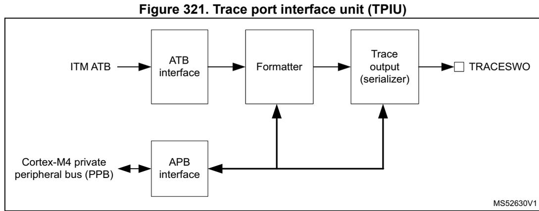
    graph LR
        subgraph TPIU [Trace port interface unit (TPIU)]
            direction LR
            ITM_ATB[ITM ATB] --> ATB_interface[ATB interface]
            ATB_interface --> Formatter[Formatter]
            Formatter --> Trace_output[Trace output (serializer)]
            Trace_output --> TRACESWO[TRACESWO]
            PPB[Cortex-M4 private peripheral bus (PPB)] <--> APB_interface[APB interface]
            APB_interface --> Formatter
            APB_interface --> Trace_output
        end
Trace data can be output on the serial wire output, TRACESWO.
For more information on the Trace Port Interface in the CPU1 refer to the Arm® Cortex®-M4 Technical Reference Manual [2].
33.17.1 TPIU supported port size register (TPIU_SSPSR)
Address offset: 0x000
Reset value: 0x0000 000F
| 31 | 30 | 29 | 28 | 27 | 26 | 25 | 24 | 23 | 22 | 21 | 20 | 19 | 18 | 17 | 16 |
|---|---|---|---|---|---|---|---|---|---|---|---|---|---|---|---|
| PORTSIZE[31:16] | |||||||||||||||
| r | r | r | r | r | r | r | r | r | r | r | r | r | r | r | r |
| 15 | 14 | 13 | 12 | 11 | 10 | 9 | 8 | 7 | 6 | 5 | 4 | 3 | 2 | 1 | 0 |
| PORTSIZE[15:0] | |||||||||||||||
| r | r | r | r | r | r | r | r | r | r | r | r | r | r | r | r |
Bits 31:0 PORTSIZE[31:0] : Indicates supported trace port sizes, from 1 to 32 pins. Bit n-1 when set indicates that port size n is supported.
0x0000 000F: No parallel trace port is implemented
33.17.2 TPIU current port size register (TPIU_CSPSR)
Address offset: 0x004
Reset value: 0x0000 0001
| 31 | 30 | 29 | 28 | 27 | 26 | 25 | 24 | 23 | 22 | 21 | 20 | 19 | 18 | 17 | 16 |
| PORTSIZE[31:16] | |||||||||||||||
| r | r | r | r | r | r | r | r | r | r | r | r | r | r | r | r |
| 15 | 14 | 13 | 12 | 11 | 10 | 9 | 8 | 7 | 6 | 5 | 4 | 3 | 2 | 1 | 0 |
| PORTSIZE[15:0] | |||||||||||||||
| r | r | r | r | r | r | r | r | r | r | r | r | r | r | r | r |
Bits 31:0 PORTSIZE[31:0] : Indicates current trace port size. No parallel trace port is implemented.
33.17.3 TPIU asynchronous clock prescaler register (TPIU_ACPR)
Address offset: 0x010
Reset value: 0x0000 0000
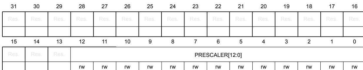
| 31 | 30 | 29 | 28 | 27 | 26 | 25 | 24 | 23 | 22 | 21 | 20 | 19 | 18 | 17 | 16 |
| Res. | Res. | Res. | Res. | Res. | Res. | Res. | Res. | Res. | Res. | Res. | Res. | Res. | Res. | Res. | Res. |
| 15 | 14 | 13 | 12 | 11 | 10 | 9 | 8 | 7 | 6 | 5 | 4 | 3 | 2 | 1 | 0 |
| Res. | Res. | Res. | PRESCALER[12:0] | ||||||||||||
| rw | rw | rw | rw | rw | rw | rw | rw | rw | rw | rw | rw | rw | |||
Bits 31:13 Reserved, must be kept at reset value.
Bits 12:0 PRESCALER[12:0] : Selects the baud rate for the asynchronous output, TRACESWO. The baud rate is given by the TRACECLKIN frequency divided by (PRESCALER +1).
33.17.4 TPIU selected pin protocol register (TPIU_SPPR)
Address offset: 0x0F0
Reset value: 0x0000 0001
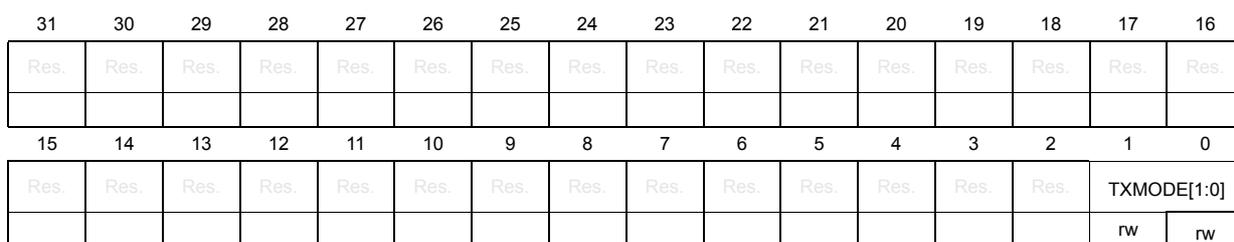
| 31 | 30 | 29 | 28 | 27 | 26 | 25 | 24 | 23 | 22 | 21 | 20 | 19 | 18 | 17 | 16 |
| Res. | Res. | Res. | Res. | Res. | Res. | Res. | Res. | Res. | Res. | Res. | Res. | Res. | Res. | Res. | Res. |
| 15 | 14 | 13 | 12 | 11 | 10 | 9 | 8 | 7 | 6 | 5 | 4 | 3 | 2 | 1 | 0 |
| Res. | Res. | Res. | Res. | Res. | Res. | Res. | Res. | Res. | Res. | Res. | Res. | Res. | Res. | TXMODE[1:0] | |
| rw | rw | ||||||||||||||
Bits 31:2 Reserved, must be kept at reset value.
Bits 1:0 TXMODE[1:0] : Selects the protocol used for trace output.
0x0: Reserved
0x1: Asynchronous SWO using Manchester encoding
0x2: Asynchronous SWO using NRZ encoding
0x3: Reserved
33.17.5 TPIU formatter and flush status register (TPIU_FFSR)
Address offset: 0x300
Reset value: 0x0000 0008
| 31 | 30 | 29 | 28 | 27 | 26 | 25 | 24 | 23 | 22 | 21 | 20 | 19 | 18 | 17 | 16 |
|---|---|---|---|---|---|---|---|---|---|---|---|---|---|---|---|
| Res. | Res. | Res. | Res. | Res. | Res. | Res. | Res. | Res. | Res. | Res. | Res. | Res. | Res. | Res. | Res. |
| 15 | 14 | 13 | 12 | 11 | 10 | 9 | 8 | 7 | 6 | 5 | 4 | 3 | 2 | 1 | 0 |
| Res. | Res. | Res. | Res. | Res. | Res. | Res. | Res. | Res. | Res. | Res. | Res. | FTNONSTOP | TCPPRESENT | FTSTOPPED | FLINPROG |
| r | r | r | r |
Bits 31:4 Reserved, must be kept at reset value.
Bit 3 FTNONSTOP : Indicates whether formatter can be stopped or not.
1: Formatter cannot be stopped
Bit 2 TCPPRESENT : Indicates whether the optional TRACECTL output pin is available for use.
0: TRACECTL pin is not present in this device.
Bit 1 FTSTOPPED : The formatter has received a stop request signal and all trace data and post-amble is sent. Any additional trace data on the ATB interface is ignored.
0: Formatter has not stopped
1: Formatter has stopped
Bit 0 FLINPROG : Flush in progress. Indicates whether a flush on the ATB slave port is in progress. This bit reflects the status of the AFVALIDS output. A flush can be initiated by the flush control bits in the TPIU_FFCR register.
0: No flush in progress
1: Flush in progress
33.17.6 TPIU formatter and flush control register (TPIU_FFCR)
Address offset: 0x304
Reset value: 0x0000 0102
| 31 | 30 | 29 | 28 | 27 | 26 | 25 | 24 | 23 | 22 | 21 | 20 | 19 | 18 | 17 | 16 |
|---|---|---|---|---|---|---|---|---|---|---|---|---|---|---|---|
| Res. | Res. | Res. | Res. | Res. | Res. | Res. | Res. | Res. | Res. | Res. | Res. | Res. | Res. | Res. | Res. |
| 15 | 14 | 13 | 12 | 11 | 10 | 9 | 8 | 7 | 6 | 5 | 4 | 3 | 2 | 1 | 0 |
| Res. | Res. | Res. | Res. | Res. | Res. | Res. | TRIGIN | Res. | Res. | Res. | Res. | Res. | Res. | ENFCONT | Res. |
| r | rw |
Bits 31:9 Reserved, must be kept at reset value.
Bit 8 TRIGIN : Trigger on trigger in.
1: Indicate a trigger in the trace stream when the TRIGIN input is asserted.
Bits 7:2 Reserved, must be kept at reset value.
Bit 1 ENFCONT : Enable continuous formatting. Setting this bit to zero in SWO mode bypasses the formatter and only ITM/DWT trace is output.
0: Continuous formatting is disabled
1: Continuous formatting is enabled
Bit 0 Reserved, must be kept at reset value.
33.17.7 TPIU formatter synchronization counter register (TPIU_FSCR)
Address offset: 0x308
Reset value: 0x0000 0040
| 31 | 30 | 29 | 28 | 27 | 26 | 25 | 24 | 23 | 22 | 21 | 20 | 19 | 18 | 17 | 16 |
|---|---|---|---|---|---|---|---|---|---|---|---|---|---|---|---|
| Res. | Res. | Res. | Res. | Res. | Res. | Res. | Res. | Res. | Res. | Res. | Res. | Res. | Res. | Res. | Res. |
| 15 | 14 | 13 | 12 | 11 | 10 | 9 | 8 | 7 | 6 | 5 | 4 | 3 | 2 | 1 | 0 |
| Res. | Res. | Res. | CYCCOUNT[12:0] | ||||||||||||
| rw | rw | rw | rw | rw | rw | rw | rw | rw | rw | rw | rw | rw | |||
Bits 31:13 Reserved, must be kept at reset value.
Bits 12:0 CYCCOUNT[12:0] : Enables effective use of different sized TPAs without wasting large amounts of the storage capacity of the capture device. This counter contains the number of formatter frames since the last synchronization packet of 128 bits. It is a 12-bit counter with a maximum count value of 4096. This equates to synchronization every 65536 bytes, that is, 4096 packets x 16 bytes per packet. The default is set up for a synchronization packet every 1024 bytes, that is, every 64 formatter frames. If the formatter is configured for continuous mode, full and half-word sync frames are inserted during normal operation. Under these circumstances, the count value is the maximum number of complete frames between full synchronization packets.
33.17.8 TPIU claim tag set register (TPIU_CLAIMSETR)
Address offset: 0xFA0
Reset value: 0x0000 000F
| 31 | 30 | 29 | 28 | 27 | 26 | 25 | 24 | 23 | 22 | 21 | 20 | 19 | 18 | 17 | 16 |
|---|---|---|---|---|---|---|---|---|---|---|---|---|---|---|---|
| Res. | Res. | Res. | Res. | Res. | Res. | Res. | Res. | Res. | Res. | Res. | Res. | Res. | Res. | Res. | Res. |
| 15 | 14 | 13 | 12 | 11 | 10 | 9 | 8 | 7 | 6 | 5 | 4 | 3 | 2 | 1 | 0 |
| Res. | Res. | Res. | Res. | Res. | Res. | Res. | Res. | Res. | Res. | Res. | Res. | CLAIMSET[3:0] | |||
| rw | rw | rw | rw | ||||||||||||
Bits 31:4 Reserved, must be kept at reset value.
Bits 3:0 CLAIMSET[3:0] : Set claim tag bits
Write:
- 0000: No effect
- xxx1: Set bit 0
- xx1x: Set bit 1
- x1xx: Set bit 2
- 1xxx: Set bit 3
Read:
0xF: Indicates there are four bits in claim tag
33.17.9 TPIU claim tag clear register (TPIU_CLAIMCLR)
Address offset: 0xFA4
Reset value: 0x0000 0000
| 31 | 30 | 29 | 28 | 27 | 26 | 25 | 24 | 23 | 22 | 21 | 20 | 19 | 18 | 17 | 16 |
|---|---|---|---|---|---|---|---|---|---|---|---|---|---|---|---|
| Res. | Res. | Res. | Res. | Res. | Res. | Res. | Res. | Res. | Res. | Res. | Res. | Res. | Res. | Res. | Res. |
| 15 | 14 | 13 | 12 | 11 | 10 | 9 | 8 | 7 | 6 | 5 | 4 | 3 | 2 | 1 | 0 |
| Res. | Res. | Res. | Res. | Res. | Res. | Res. | Res. | Res. | Res. | Res. | Res. | CLAIMCLR[3:0] | |||
| nw | nw | nw | nw | ||||||||||||
Bits 31:4 Reserved, must be kept at reset value.
Bits 3:0 CLAIMCLR[3:0] : Reset claim tag bits
Write:
- 0000: No effect
- xxx1: Clear bit 0
- xx1x: Clear bit 1
- x1xx: Clear bit 2
- 1xxx: Clear bit 3
Read: Returns current value of claim tag
33.17.10 TPIU device configuration register (TPIU_DEVIDR)
Address offset: 0xFC8
Reset value: 0x0000 0CA1
| 31 | 30 | 29 | 28 | 27 | 26 | 25 | 24 | 23 | 22 | 21 | 20 | 19 | 18 | 17 | 16 |
|---|---|---|---|---|---|---|---|---|---|---|---|---|---|---|---|
| Res. | Res. | Res. | Res. | Res. | Res. | Res. | Res. | Res. | Res. | Res. | Res. | Res. | Res. | Res. | Res. |
| 15 | 14 | 13 | 12 | 11 | 10 | 9 | 8 | 7 | 6 | 5 | 4 | 3 | 2 | 1 | 0 |
| Res. | Res. | Res. | Res. | SWO UARTNRZ | SWO MAN | TCLK DATA | FIFO SIZE[2:0] | CLK RELAT | MAXNUM[3:0] | ||||||
| r | r | r | r | r | r | r | r | r | r | r | r | ||||
Bits 31:11 Reserved, must be kept at reset value.
- Bit 11
SWONRZ
: Indicates whether Serial wire output, NRZ, is supported.
0x1: Supported - Bit 10
SWOMAN
: Indicates whether Serial wire output, Manchester encoded format, is supported.
0x1: Supported - Bit 9
TCLKDATA
: Indicates whether trace clock plus data is supported
0x0: Supported - Bits 8:6
FIFOSIZE[2:0]
: FIFO size in powers of 2
0x2: FIFO size = 4 bytes - Bit 5
CLKRELAT
: Indicates the relationship between the ATB clock and TRACECLKIN (synchronous or asynchronous)
0x1: Asynchronous - Bits 4:0
MAXNUM[4:0]
: Number/type of ATB input port multiplexing
0x1: Two input ports, only one port is used in this product
33.17.11 TPIU device type identifier register (TPIU_DEVTYPE)
Address offset: 0xFCC
Reset value: 0x0000 0011
| 31 | 30 | 29 | 28 | 27 | 26 | 25 | 24 | 23 | 22 | 21 | 20 | 19 | 18 | 17 | 16 |
|---|---|---|---|---|---|---|---|---|---|---|---|---|---|---|---|
| Res. | Res. | Res. | Res. | Res. | Res. | Res. | Res. | Res. | Res. | Res. | Res. | Res. | Res. | Res. | Res. |
| 15 | 14 | 13 | 12 | 11 | 10 | 9 | 8 | 7 | 6 | 5 | 4 | 3 | 2 | 1 | 0 |
| Res. | Res. | Res. | Res. | Res. | Res. | Res. | Res. | SUBTYPE[3:0] | MAJORTYPE[3:0] | ||||||
| r | r | r | r | r | r | r | r | ||||||||
Bits 31:8 Reserved, must be kept at reset value.
Bits 7:4 SUBTYPE[3:0] : Sub-classification
0x1: Trace port component
Bits 3:0 MAJORTYPE[3:0] : Major classification
0x1: Trace sink component
33.17.12 TPIU CoreSight peripheral identity register 4 (TPIU_PIDR4)
Address offset: 0xFD0
Reset value: 0x0000 0004
| 31 | 30 | 29 | 28 | 27 | 26 | 25 | 24 | 23 | 22 | 21 | 20 | 19 | 18 | 17 | 16 |
|---|---|---|---|---|---|---|---|---|---|---|---|---|---|---|---|
| Res. | Res. | Res. | Res. | Res. | Res. | Res. | Res. | Res. | Res. | Res. | Res. | Res. | Res. | Res. | Res. |
| 15 | 14 | 13 | 12 | 11 | 10 | 9 | 8 | 7 | 6 | 5 | 4 | 3 | 2 | 1 | 0 |
| Res. | Res. | Res. | Res. | Res. | Res. | Res. | Res. | 4KCOUNT[3:0] | JEP106CON[3:0] | ||||||
| r | r | r | r | r | r | r | r | ||||||||
Bits 31:8 Reserved, must be kept at reset value.
Bits 7:4 4KCOUNT[3:0] : register file size
0x0: Register file occupies a single 4 KB region
Bits 3:0 JEP106CON[3:0] : JEP106 continuation code
0x4: Arm® JEDEC code
33.17.13 TPIU CoreSight peripheral identity register 0 (TPIU_PIDR0)
Address offset: 0xFE0
Reset value: 0x0000 00A1
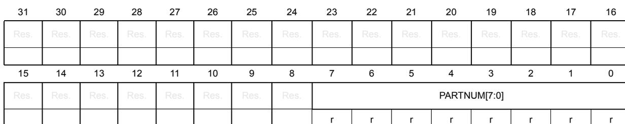
| 31 | 30 | 29 | 28 | 27 | 26 | 25 | 24 | 23 | 22 | 21 | 20 | 19 | 18 | 17 | 16 |
|---|---|---|---|---|---|---|---|---|---|---|---|---|---|---|---|
| Res. | Res. | Res. | Res. | Res. | Res. | Res. | Res. | Res. | Res. | Res. | Res. | Res. | Res. | Res. | Res. |
| 15 | 14 | 13 | 12 | 11 | 10 | 9 | 8 | 7 | 6 | 5 | 4 | 3 | 2 | 1 | 0 |
|---|---|---|---|---|---|---|---|---|---|---|---|---|---|---|---|
| Res. | Res. | Res. | Res. | Res. | Res. | Res. | Res. | PARTNUM[7:0] | |||||||
| r | r | r | r | r | r | r | r | ||||||||
Bits 31:8 Reserved, must be kept at reset value.
Bits 7:0 PARTNUM[7:0] : Part number bits [7:0]
0xA1: CPU1 TPIU part number
33.17.14 TPIU CoreSight peripheral identity register 1 (TPIU_PIDR1)
Address offset: 0xFE4
Reset value: 0x0000 00B9
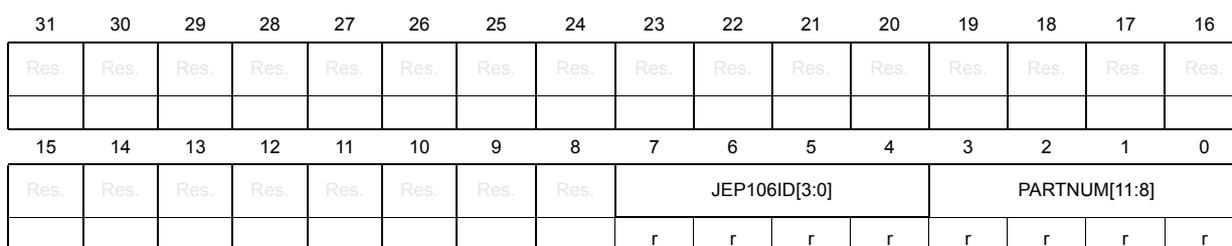
| 31 | 30 | 29 | 28 | 27 | 26 | 25 | 24 | 23 | 22 | 21 | 20 | 19 | 18 | 17 | 16 |
|---|---|---|---|---|---|---|---|---|---|---|---|---|---|---|---|
| Res. | Res. | Res. | Res. | Res. | Res. | Res. | Res. | Res. | Res. | Res. | Res. | Res. | Res. | Res. | Res. |
| 15 | 14 | 13 | 12 | 11 | 10 | 9 | 8 | 7 | 6 | 5 | 4 | 3 | 2 | 1 | 0 |
|---|---|---|---|---|---|---|---|---|---|---|---|---|---|---|---|
| Res. | Res. | Res. | Res. | Res. | Res. | Res. | Res. | JEP106ID[3:0] | PARTNUM[11:8] | ||||||
| r | r | r | r | r | r | r | r | ||||||||
Bit 31:8 Reserved, must be kept at reset value.
Bits 7:4 JEP106ID[3:0] : JEP106 identity code bits [3:0]
0xB: Arm® JEDEC code
Bits 3:0 PARTNUM[11:8] : Part number bits [11:8]
0x9: CPU1 TPIU part number
33.17.15 TPIU CoreSight peripheral identity register 2 (TPIU_PIDR2)
Address offset: 0xFE8
Reset value: 0x0000 004B
| 31 | 30 | 29 | 28 | 27 | 26 | 25 | 24 | 23 | 22 | 21 | 20 | 19 | 18 | 17 | 16 |
|---|---|---|---|---|---|---|---|---|---|---|---|---|---|---|---|
| Res. | Res. | Res. | Res. | Res. | Res. | Res. | Res. | Res. | Res. | Res. | Res. | Res. | Res. | Res. | Res. |
| 15 | 14 | 13 | 12 | 11 | 10 | 9 | 8 | 7 | 6 | 5 | 4 | 3 | 2 | 1 | 0 |
| Res. | Res. | Res. | Res. | Res. | Res. | Res. | Res. | REVISION[3:0] | JEDEC | JEP106ID[6:4] | |||||
| r | r | r | r | r | r | r | r | ||||||||
Bit 31:8 Reserved, must be kept at reset value.
Bits 7:4 REVISION[3:0] : Component revision number
0x4: r0p5
Bit 3 JEDEC : JEDEC assigned value
0x1: Designer ID specified by JEDEC
Bits 2:0 JEP106ID[6:4] : JEP106 identity code bits [6:4]
0x3: Arm® JEDEC code
33.17.16 TPIU CoreSight peripheral identity register 3 (TPIU_PIDR3)
Address offset: 0xFEC
Reset value: 0x0000 0000
| 31 | 30 | 29 | 28 | 27 | 26 | 25 | 24 | 23 | 22 | 21 | 20 | 19 | 18 | 17 | 16 |
|---|---|---|---|---|---|---|---|---|---|---|---|---|---|---|---|
| Res. | Res. | Res. | Res. | Res. | Res. | Res. | Res. | Res. | Res. | Res. | Res. | Res. | Res. | Res. | Res. |
| 15 | 14 | 13 | 12 | 11 | 10 | 9 | 8 | 7 | 6 | 5 | 4 | 3 | 2 | 1 | 0 |
| Res. | Res. | Res. | Res. | Res. | Res. | Res. | Res. | REVAND[3:0] | CMOD[3:0] | ||||||
| r | r | r | r | r | r | r | r | ||||||||
Bit 31:8 Reserved, must be kept at reset value.
Bits 7:4 REVAND[3:0] : metal fix version
0x0: No metal fix
Bits 3:0 CMOD[3:0] : Customer modified
0x0: No customer modifications
33.17.17 TPIU CoreSight component identity register 0 (TPIU_CIDR0)
Address offset: 0xFF0
Reset value: 0x0000 000D
| 31 | 30 | 29 | 28 | 27 | 26 | 25 | 24 | 23 | 22 | 21 | 20 | 19 | 18 | 17 | 16 |
|---|---|---|---|---|---|---|---|---|---|---|---|---|---|---|---|
| Res. | Res. | Res. | Res. | Res. | Res. | Res. | Res. | Res. | Res. | Res. | Res. | Res. | Res. | Res. | Res. |
| 15 | 14 | 13 | 12 | 11 | 10 | 9 | 8 | 7 | 6 | 5 | 4 | 3 | 2 | 1 | 0 |
| Res. | Res. | Res. | Res. | Res. | Res. | Res. | Res. | PREAMBLE[7:0] | |||||||
| r | r | r | r | r | r | r | r | ||||||||
Bits 31:8 Reserved, must be kept at reset value.
Bits 7:0 PREAMBLE[7:0] : Component ID bits [7:0]
0x0D: Common ID value
33.17.18 TPIU CoreSight peripheral identity register 1 (TPIU_CIDR1)
Address offset: 0xFF4
Reset value: 0x0000 0090
| 31 | 30 | 29 | 28 | 27 | 26 | 25 | 24 | 23 | 22 | 21 | 20 | 19 | 18 | 17 | 16 |
|---|---|---|---|---|---|---|---|---|---|---|---|---|---|---|---|
| Res. | Res. | Res. | Res. | Res. | Res. | Res. | Res. | Res. | Res. | Res. | Res. | Res. | Res. | Res. | Res. |
| 15 | 14 | 13 | 12 | 11 | 10 | 9 | 8 | 7 | 6 | 5 | 4 | 3 | 2 | 1 | 0 |
| Res. | Res. | Res. | Res. | Res. | Res. | Res. | Res. | CLASS[3:0] | PREAMBLE[11:8] | ||||||
| r | r | r | r | r | r | r | r | ||||||||
Bit 31:8 Reserved, must be kept at reset value.
Bits 7:4 CLASS[3:0] : Component ID bits [15:12] - component class
0x9: CoreSight™ component
Bits 3:0 PREAMBLE[11:8] : Component ID bits [11:8]
0x0: Common ID value
33.17.19 TPIU CoreSight component identity register 2 (TPIU_CIDR2)
Address offset: 0xFF8
Reset value: 0x0000 0005
| 31 | 30 | 29 | 28 | 27 | 26 | 25 | 24 | 23 | 22 | 21 | 20 | 19 | 18 | 17 | 16 |
|---|---|---|---|---|---|---|---|---|---|---|---|---|---|---|---|
| Res. | Res. | Res. | Res. | Res. | Res. | Res. | Res. | Res. | Res. | Res. | Res. | Res. | Res. | Res. | Res. |
| 15 | 14 | 13 | 12 | 11 | 10 | 9 | 8 | 7 | 6 | 5 | 4 | 3 | 2 | 1 | 0 |
| Res. | Res. | Res. | Res. | Res. | Res. | Res. | Res. | PREAMBLE[19:12] | |||||||
| r | r | r | r | r | r | r | r | ||||||||
Bits 31:8 Reserved, must be kept at reset value.
Bits 7:0
PREAMBLE[19:12]
: Component ID bits [23:16]
0x05: Common ID value
33.17.20 TPIU CoreSight component identity register 3 (TPIU_CIDR3)
Address offset: 0xFFC
Reset value: 0x0000 00B1
| 31 | 30 | 29 | 28 | 27 | 26 | 25 | 24 | 23 | 22 | 21 | 20 | 19 | 18 | 17 | 16 |
|---|---|---|---|---|---|---|---|---|---|---|---|---|---|---|---|
| Res. | Res. | Res. | Res. | Res. | Res. | Res. | Res. | Res. | Res. | Res. | Res. | Res. | Res. | Res. | Res. |
| 15 | 14 | 13 | 12 | 11 | 10 | 9 | 8 | 7 | 6 | 5 | 4 | 3 | 2 | 1 | 0 |
| Res. | Res. | Res. | Res. | Res. | Res. | Res. | Res. | PREAMBLE[27:20] | |||||||
| r | r | r | r | r | r | r | r | ||||||||
Bits 31:8 Reserved, must be kept at reset value.
Bits 7:0
PREAMBLE[27:20]
: Component ID bits [31:24]
0xB1: Common ID value
33.17.21 CPU1 TPIU register map and reset values
Table 231. CPU1 TPIU register map and reset values
| Offset | Register name | 31 | 30 | 29 | 28 | 27 | 26 | 25 | 24 | 23 | 22 | 21 | 20 | 19 | 18 | 17 | 16 | 15 | 14 | 13 | 12 | 11 | 10 | 9 | 8 | 7 | 6 | 5 | 4 | 3 | 2 | 1 | 0 | |
|---|---|---|---|---|---|---|---|---|---|---|---|---|---|---|---|---|---|---|---|---|---|---|---|---|---|---|---|---|---|---|---|---|---|---|
| 0x000 | TPIU_SSPSR | PORTSIZE[31:0] | ||||||||||||||||||||||||||||||||
| Reset value | 0 | 0 | 0 | 0 | 0 | 0 | 0 | 0 | 0 | 0 | 0 | 0 | 0 | 0 | 0 | 0 | 0 | 0 | 0 | 0 | 0 | 0 | 0 | 0 | 0 | 0 | 0 | 0 | 0 | 1 | 1 | 1 | ||
| 0x004 | TPIU_CSPSR | PORTSIZE[31:0] | ||||||||||||||||||||||||||||||||
| Reset value | 0 | 0 | 0 | 0 | 0 | 0 | 0 | 0 | 0 | 0 | 0 | 0 | 0 | 0 | 0 | 0 | 0 | 0 | 0 | 0 | 0 | 0 | 0 | 0 | 0 | 0 | 0 | 0 | 0 | 0 | 0 | 1 | ||
| 0x010 | TPIU_ACPR | Res. | Res. | Res. | Res. | Res. | Res. | Res. | Res. | Res. | Res. | Res. | Res. | Res. | Res. | Res. | Res. | Res. | Res. | Res. | PRESCALER[12:0] | |||||||||||||
| Reset value | 0 | 0 | 0 | 0 | 0 | 0 | 0 | 0 | 0 | 0 | 0 | 0 | 0 | |||||||||||||||||||||
| 0x0F0 | TPIU_SPPR | Res. | Res. | Res. | Res. | Res. | Res. | Res. | Res. | Res. | Res. | Res. | Res. | Res. | Res. | Res. | Res. | Res. | Res. | Res. | Res. | Res. | Res. | Res. | Res. | Res. | Res. | Res. | Res. | Res. | Res. | Res. | TXMODE[1:0] | |
| Reset value | 0 | |||||||||||||||||||||||||||||||||
| 0x300 | TPIU_FFSR | Res. | Res. | Res. | Res. | Res. | Res. | Res. | Res. | Res. | Res. | Res. | Res. | Res. | Res. | Res. | Res. | Res. | Res. | Res. | Res. | Res. | Res. | Res. | Res. | Res. | Res. | Res. | Res. | FTNONSTOP | TOPRESENT | FTSTOPPED | FLINPROG | |
| Reset value | 1 | 0 | 0 | 0 | ||||||||||||||||||||||||||||||
| 0x304 | TPIU_FFCR | Res. | Res. | Res. | Res. | Res. | Res. | Res. | Res. | Res. | Res. | Res. | Res. | Res. | Res. | Res. | Res. | Res. | Res. | Res. | Res. | Res. | Res. | TRIGIN | Res. | Res. | Res. | Res. | Res. | Res. | Res. | ENFCONT | Res. | |
| Reset value | 1 | 1 | ||||||||||||||||||||||||||||||||
| 0x308 | TPIU_FSCR | Res. | Res. | Res. | Res. | Res. | Res. | Res. | Res. | Res. | Res. | Res. | Res. | Res. | Res. | Res. | Res. | Res. | Res. | Res. | CYCCOUNT[11:0] | |||||||||||||
| Reset value | 0 | 0 | 0 | 0 | 0 | 0 | 0 | 0 | 0 | 0 | 0 | 0 | 0 | |||||||||||||||||||||
| 0xFA0 | TPIU_CLAIMSETR | Res. | Res. | Res. | Res. | Res. | Res. | Res. | Res. | Res. | Res. | Res. | Res. | Res. | Res. | Res. | Res. | Res. | Res. | Res. | Res. | Res. | Res. | Res. | Res. | Res. | Res. | Res. | Res. | Res. | Res. | CLAIMSET[3:0] | ||
| Reset value | 1 | 1 | ||||||||||||||||||||||||||||||||
| 0xFA4 | TPIU_CLAIMCLR | Res. | Res. | Res. | Res. | Res. | Res. | Res. | Res. | Res. | Res. | Res. | Res. | Res. | Res. | Res. | Res. | Res. | Res. | Res. | Res. | Res. | Res. | Res. | Res. | Res. | Res. | Res. | Res. | Res. | Res. | CLAIMCLR[3:0] | ||
| Reset value | 0 | 0 | ||||||||||||||||||||||||||||||||
| 0xFC8 | TPIU_DEVIDR | Res. | Res. | Res. | Res. | Res. | Res. | Res. | Res. | Res. | Res. | Res. | Res. | Res. | Res. | Res. | Res. | Res. | Res. | Res. | SWONRZ | SWOMAN | TCLKDATA | FIFOSIZE[2:0] | CLKRELAT | MUXNUM[4:0] | ||||||||
| Reset value | 1 | 1 | 0 | 0 | 1 | 0 | 1 | 0 | 0 | 0 | 0 | 0 | 1 | |||||||||||||||||||||
| 0xFD0 | TPIU_DEVTYPE | Res. | Res. | Res. | Res. | Res. | Res. | Res. | Res. | Res. | Res. | Res. | Res. | Res. | Res. | Res. | Res. | Res. | Res. | Res. | Res. | Res. | Res. | SUBTYPE [3:0] | MAJORTYPE [3:0] | |||||||||
| Reset value | 0 | 0 | 0 | 1 | 0 | 0 | 0 | 0 | 1 | |||||||||||||||||||||||||
| 0xFD0 | TPIU_PIDR4 | Res. | Res. | Res. | Res. | Res. | Res. | Res. | Res. | Res. | Res. | Res. | Res. | Res. | Res. | Res. | Res. | Res. | Res. | Res. | 4KCOUNT [3:0] | JEP106CON [3:0] | ||||||||||||
| Reset value | 0 | 0 | 0 | 0 | 0 | 0 | 0 | 0 | 0 | 1 | 0 | 0 | 0 | |||||||||||||||||||||
Table 231. CPU1 TPIU register map and reset values (continued)
| Offset | Register name | 31 | 30 | 29 | 28 | 27 | 26 | 25 | 24 | 23 | 22 | 21 | 20 | 19 | 18 | 17 | 16 | 15 | 14 | 13 | 12 | 11 | 10 | 9 | 8 | 7 | 6 | 5 | 4 | 3 | 2 | 1 | 0 | |
|---|---|---|---|---|---|---|---|---|---|---|---|---|---|---|---|---|---|---|---|---|---|---|---|---|---|---|---|---|---|---|---|---|---|---|
| 0xFD4 | TPIU_PIDR5 | Res | Res | Res | Res | Res | Res | Res | Res | Res | Res | Res | Res | Res | Res | Res | Res | Res | Res | Res | Res | Res | Res | Res | Res | Res | Res | Res | Res | Res | Res | Res | Res | Res |
| Reset value | ||||||||||||||||||||||||||||||||||
| 0xFD8 | TPIU_PIDR6 | Res | Res | Res | Res | Res | Res | Res | Res | Res | Res | Res | Res | Res | Res | Res | Res | Res | Res | Res | Res | Res | Res | Res | Res | Res | Res | Res | Res | Res | Res | Res | Res | Res |
| Reset value | ||||||||||||||||||||||||||||||||||
| 0xFDC | TPIU_PIDR7 | Res | Res | Res | Res | Res | Res | Res | Res | Res | Res | Res | Res | Res | Res | Res | Res | Res | Res | Res | Res | Res | Res | Res | Res | Res | Res | Res | Res | Res | Res | Res | Res | Res |
| Reset value | ||||||||||||||||||||||||||||||||||
| 0xFE0 | TPIU_PIDR0 | Res | Res | Res | Res | Res | Res | Res | Res | Res | Res | Res | Res | Res | Res | Res | Res | Res | Res | Res | Res | Res | Res | Res | Res | PARTNUM[7:0] | ||||||||
| Reset value | 1 | 0 | 1 | 0 | 0 | 0 | 0 | 1 | ||||||||||||||||||||||||||
| 0xFE4 | TPIU_PIDR1 | Res | Res | Res | Res | Res | Res | Res | Res | Res | Res | Res | Res | Res | Res | Res | Res | Res | Res | Res | Res | Res | Res | Res | Res | JEP106ID [3:0] | PARTNUM [11:8] | |||||||
| Reset value | 1 | 0 | 1 | 1 | 1 | 0 | 0 | 1 | ||||||||||||||||||||||||||
| 0xFE8 | TPIU_PIDR2 | Res | Res | Res | Res | Res | Res | Res | Res | Res | Res | Res | Res | Res | Res | Res | Res | Res | Res | Res | Res | Res | Res | Res | Res | REVISION [3:0] | JEDEC | JEP106ID [6:4] | ||||||
| Reset value | 0 | 0 | 0 | 1 | 0 | 1 | 1 | |||||||||||||||||||||||||||
| 0xFEC | TPIU_PIDR3 | Res | Res | Res | Res | Res | Res | Res | Res | Res | Res | Res | Res | Res | Res | Res | Res | Res | Res | Res | Res | Res | Res | Res | Res | REVAND[3:0] | CMOD[3:0] | |||||||
| Reset value | 0 | 0 | 0 | 0 | 0 | 0 | 0 | 0 | ||||||||||||||||||||||||||
| 0xFF0 | TPIU_CIDR0 | Res | Res | Res | Res | Res | Res | Res | Res | Res | Res | Res | Res | Res | Res | Res | Res | Res | Res | Res | Res | Res | Res | Res | Res | PREAMBLE[7:0] | ||||||||
| Reset value | 0 | 0 | 0 | 0 | 1 | 1 | 0 | 1 | ||||||||||||||||||||||||||
| 0xFF4 | TPIU_CIDR1 | Res | Res | Res | Res | Res | Res | Res | Res | Res | Res | Res | Res | Res | Res | Res | Res | Res | Res | Res | Res | Res | Res | Res | Res | CLASS[3:0] | PREAMBLE [11:8] | |||||||
| Reset value | 1 | 0 | 0 | 1 | 0 | 0 | 0 | 0 | ||||||||||||||||||||||||||
| 0xFF8 | TPIU_CIDR2 | Res | Res | Res | Res | Res | Res | Res | Res | Res | Res | Res | Res | Res | Res | Res | Res | Res | Res | Res | Res | Res | Res | Res | Res | PREAMBLE[19:12] | ||||||||
| Reset value | 0 | 0 | 0 | 0 | 0 | 1 | 0 | 1 | ||||||||||||||||||||||||||
| 0xFFC | TPIU_CIDR3 | Res | Res | Res | Res | Res | Res | Res | Res | Res | Res | Res | Res | Res | Res | Res | Res | Res | Res | Res | Res | Res | Res | Res | Res | PREAMBLE[27:20] | ||||||||
| Reset value | 1 | 0 | 1 | 1 | 0 | 0 | 0 | 1 | ||||||||||||||||||||||||||
33.18 CPU1 cross trigger interface (CTI)
See Section 33.6: Cross trigger interface (CTI) and matrix (CTM) .
33.19 References
- 1. IHI 0031C (ID080813) - Arm ® Debug Interface Architecture Specification ADIv5.0 to ADIv5.2, Issue C, 8 Aug 2013
- 2. DDI 0480F (ID100313) - Arm ® CoreSight ™ SoC-400 r3p2 Technical Reference Manual, Issue G, 16 March 2015
- 3. DDI 0461B (ID010111) - Arm ® CoreSight ™ Trace Memory Controller r0p1 Technical Reference Manual, Issue B, 10 Dec 2010
- 4. DDI 0314H - Arm ® CoreSight ™ Components Technical Reference Manual, Issue H, 10 July, 2009
- 5. DDI 0403D (ID100710) - Arm ® v7-M Architecture Reference Manual, Issue E.b, 2 December 2014