58. Single wire protocol master interface (SWPMI)
58.1 Introduction
The single wire protocol master interface (SWPMI) is the master interface corresponding to the contactless front-end (CLF) defined in the ETSI TS 102 613 technical specification.
The principle of the Single wire protocol (SWP) is based on the transmission of digital information in full duplex mode:
- • S1 signal (from Master to Slave) is transmitted by a digital modulation (L or H) in the voltage domain (refer to Figure 714: S1 signal coding ),
- • S2 signal (from Slave to Master) is transmitted by a digital modulation (L or H) in the current domain (refer to Figure 715: S2 signal coding ).
Figure 714. S1 signal coding
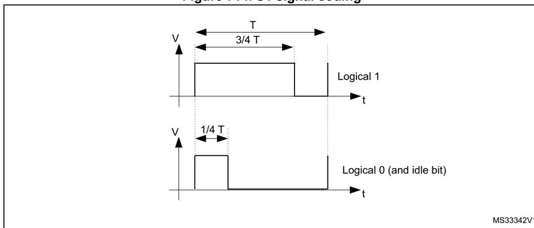
Figure 714 shows the S1 signal coding. It consists of two timing diagrams. The top diagram for 'Logical 1' shows a signal that is high for a duration of \( 3/4 T \) and low for \( 1/4 T \) . The bottom diagram for 'Logical 0 (and idle bit)' shows a signal that is high for a duration of \( 1/4 T \) and low for \( 3/4 T \) . Both diagrams show voltage (V) on the y-axis and time (t) on the x-axis. The total period is labeled as T.
MS33342V1
Figure 715. S2 signal coding
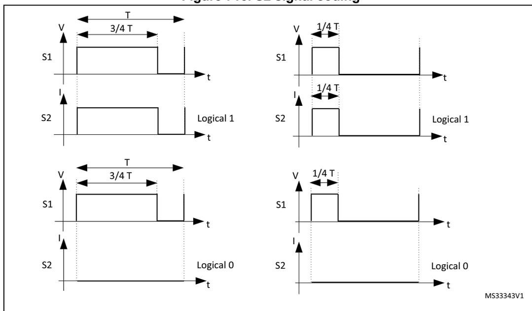
Figure 715 shows the S2 signal coding. It consists of four timing diagrams arranged in a 2x2 grid. The top-left diagram for 'Logical 1' shows the S1 signal (voltage) high for \( 3/4 T \) and the S2 signal (current) high for \( 1/4 T \) . The top-right diagram for 'Logical 1' shows S1 high for \( 1/4 T \) and S2 high for \( 1/4 T \) . The bottom-left diagram for 'Logical 0' shows the S1 signal (voltage) high for \( 3/4 T \) and the S2 signal (current) low. The bottom-right diagram for 'Logical 0' shows S1 high for \( 1/4 T \) and S2 low. All diagrams show voltage (V) or current (I) on the y-axis and time (t) on the x-axis. The total period is labeled as T.
MS33343V1
58.2 SWPMI main features
The SWPMI module main features are the following (see Figure 58.3.4: SWP bus states ):
- • Full-duplex communication mode
- • Automatic SWP bus state management
- • Automatic handling of Start of frame (SOF)
- • Automatic handling of End of frame (EOF)
- • Automatic handling of stuffing bits
- • Automatic CRC-16 calculation and generation in transmission
- • Automatic CRC-16 calculation and checking in reception
- • 32-bit Transmit data register
- • 32-bit Receive data register
- • Multi software buffer mode for efficient DMA implementation and multi frame buffering
- • Configurable bit-rate up to 2 Mbit/s
- • Configurable interrupts
- • CRC error, underrun, overrun flags
- • Frame reception and transmission complete flags
- • Slave resume detection flag
- • Loopback mode for test purpose
- • Embedded SWPMI_IO transceiver compliant with ETSI TS 102 613 technical specification
- • Dedicated mode to output SWPMI_RX, SWPMI_TX and SWPMI_SUSPEND signals on GPIOs, in case of external transceiver connection
58.3 SWPMI functional description
58.3.1 SWPMI block diagram
Figure 716. SWPMI block diagram
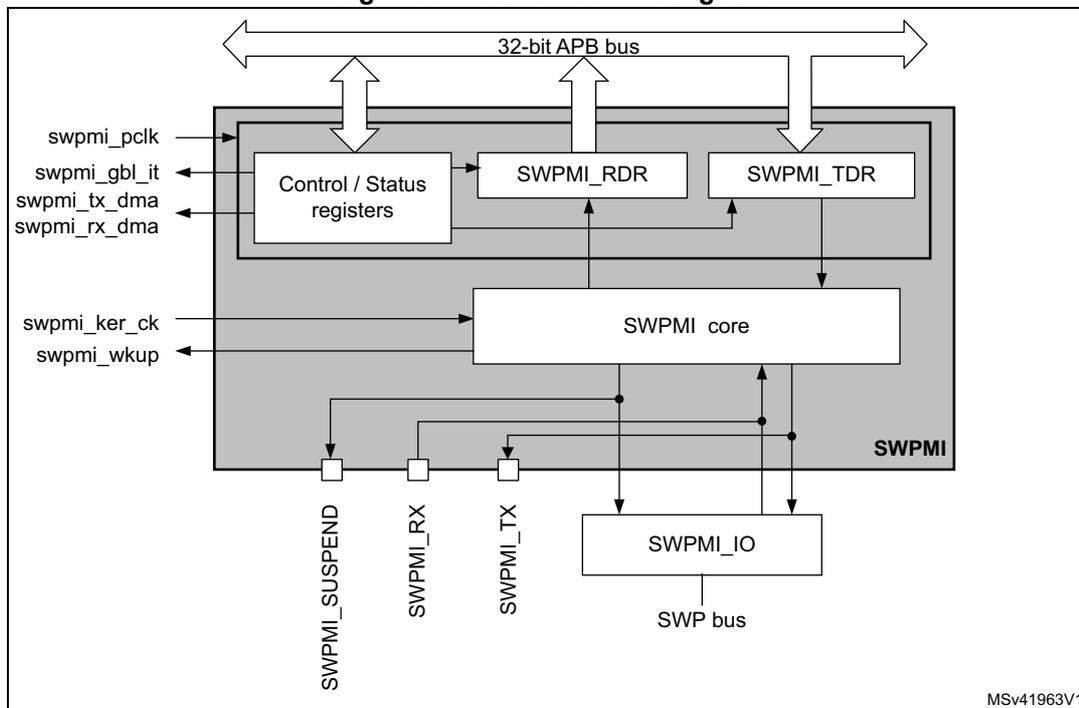
The block diagram illustrates the internal architecture of the SWPMI. A 32-bit APB bus is connected to a 'Control / Status registers' block, which in turn connects to 'SWPMI_RDR' (Receive Data Register) and 'SWPMI_TDR' (Transmit Data Register). These registers are connected to the 'SWPMI core'. The 'SWPMI core' is connected to 'SWPMI_IO', which is further connected to the 'SWP bus'. External pins are shown: 'swpmi_pclk' (input), 'swpmi_gbl_it' (output), 'swpmi_tx_dma' (output), 'swpmi_rx_dma' (output), 'swpmi_ker_ck' (input), and 'swpmi_wkup' (output). Internal pins are labeled 'SWPMI_SUSPEND', 'SWPMI_RX', and 'SWPMI_TX'. The diagram is labeled 'MSv41963V1' in the bottom right corner.
Refer to the bit
SWPSELSWPMISEL
in
Section 8.7.19: RCC domain 2 kernel clock configuration register (RCC_D2CCIP1R)
to select the
swpmi_ker_ck
(SWPMI core clock source).
Note:
In order to support the exit from Stop mode by a RESUME by slave, it is mandatory to select HSI for
swpmi_ker_ck
. If this feature is not required,
swpmi_pclk
can be selected, and SWPMI must be disabled before entering the Stop mode.
58.3.2 SWPMI pins and internal signals
Table 462 lists the SWPMI slave inputs and output signals connected to package pins or balls, while Table 463 shows the internal SWPMI signals.
Table 462. SWPMI input/output signals connected to package pins or balls
| Signal name | Signal type | Description |
|---|---|---|
| SWPMI_SUSPEND | Digital output | SWPMI suspend signal |
| SWPMI_TX | Digital output | SWPMI transmit signal |
| Signal name | Signal type | Description |
|---|---|---|
| SWPMI_RX | Digital input | SWPMI receive signal |
| SWPMI_IO | Input and output | Internal SWPMI transceiver. |
| Signal name | Signal type | Description |
|---|---|---|
| swpmi_pclk | Digital input | APB clock |
| swpmi_ker_ck | Digital input | SWPMI kernel clock |
| swpmi_wkup | Digital output | SWPMI wakeup signal |
| swpmi_gbl_it | Digital output | SWPMI interrupt signal |
| swpmi_tx_dma | Digital output | SWPMI DMA transmit request |
| swpmi_rx_dma | Digital output | SWPMI DMA receive request |
58.3.3 SWP initialization and activation
The initialization and activation will set the SWPMI_IO state from low to high.
When using the internal transceiver, the procedure is the following:
- 1. Configure the SWP_CLASS bit in SWPMI_OR register according to the VDD voltage (3 V or 1.8 V),
- 2. Set SWPTEN in SWPMI_CR register to enable the SWPMI_IO transceiver and set the SWPMI_IO to low level (SWP bus DEACTIVATED)
- 3. Wait for the RDYF flag in SWPMI_SR register to be set (polling the flag or enabling the interrupt with RDYIE bit in SWPMI_IER register),
- 4. Set SWPACT bit in SWPMI_CR register to ACTIVATE the SWP i.e. to move from DEACTIVATED to SUSPENDED.
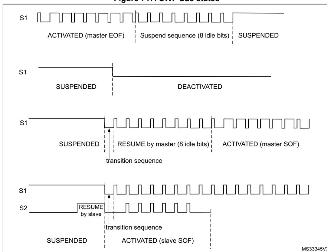
58.3.4 SWP bus states
The SWP bus can have the following states: DEACTIVATED, SUSPENDED, ACTIVATED.
Several transitions are possible:
- • ACTIVATE: transition from DEACTIVATED to SUSPENDED state,
- • SUSPEND: transition from ACTIVATED to SUSPENDED state,
- • RESUME by master: transition from SUSPENDED to ACTIVATED state initiated by the master,
- • RESUME by slave: transition from SUSPENDED to ACTIVATED state initiated by the slave,
- • DEACTIVATE: transition from SUSPENDED to DEACTIVATED state.
ACTIVATE
During and just after reset, the SWPMI_IO is configured in analog mode. Refer to Section 58.3.3: SWP initialization and activation to activate the SWP bus.
SUSPEND
The SWP bus stays in the ACTIVATED state as long as there is a communication with the slave, either in transmission or in reception. The SWP bus switches back to the SUSPENDED state as soon as there is no more transmission or reception activity, after 7 idle bits.
RESUME by master
Once the SWPMI is enabled, the user can request a SWPMI frame transmission. The SWPMI first sends a transition sequence and 8 idle bits (RESUME by master) before starting the frame transmission. The SWP moves from the SUSPENDED to ACTIVATED state after the RESUME by master (refer to Figure 717: SWP bus states ).
RESUME by slave
Once the SWPMI is enabled, the SWP can also move from the SUSPENDED to ACTIVATED state if the SWPMI receives a RESUME from the slave. The RESUME by slave sets the SRF flag in the SWPMI_ISR register.
DEACTIVATE
Deactivate request
If no more communication is required, and if SWP is in the SUSPENDED mode, the user can request to switch the SWP to the DEACTIVATED mode by disabling the SWPMI peripheral. The software must set DEACT bit in the SWPMI_CR register in order to request the DEACTIVATED mode. If no RESUME by slave is detected by SWPMI, the DEACTF flag is set in the SWPMI_ISR register and the SWPACT bit is cleared in the SWPMI_ICR register. In case a RESUME by slave is detected by the SWPMI while the software is setting DEACT bit, the SRF flag is set in the SWPMI_ISR register, DEACTF is kept cleared, SWPACT is kept set and DEACT bit is cleared.
In order to activate SWP again, the software must clear DEACT bit in the SWPMI_CR register before setting SWPACT bit.
Deactivate mode
In order to switch the SWP to the DEACTIVATED mode immediately, ignoring any possible incoming RESUME by slave, the user must clear SWPACT bit in the SWPMI_CR register.
Note: In order to further reduce current consumption, configure the SWPMI_IO port as output push pull low in GPIO controller and then clear the SWPTEN bit in SWPMI_CR register (refer to Section 8: General-purpose I/Os (GPIO)).
Figure 717. SWP bus states
58.3.5 SWPMI_IO (internal transceiver) bypass
A SWPMI_IO (transceiver), compliant with ETSI TS 102 613 technical specification, is embedded in the microcontroller. Nevertheless, this is possible to bypass it by setting SWP_TBYP bit in SWPMI_OR register. In this case, the SWPMI_IO is disabled and the SWPMI_RX, SWPMI_TX and SWPMI_SUSPEND signals are available as alternate functions on three GPIOs (refer to “Pinouts and pin description” in product datasheet). This configuration is selected to connect an external transceiver.
Note: In SWPMI_IO bypass mode, SWPTEN bit in SWPMI_CR register must be kept cleared.
58.3.6 SWPMI bit rate
The bit rate must be set in the SWPMI_BRR register, according to the following formula:
Note: The maximum bitrate is 2 Mbit/s.
58.3.7 SWPMI frame handling
The SWP frame is composed of a Start of frame (SOF), a Payload from 1 to 30 bytes, a 16-bit CRC and an End of frame (EOF) (Refer to Figure 718: SWP frame structure ).
Figure 718. SWP frame structure
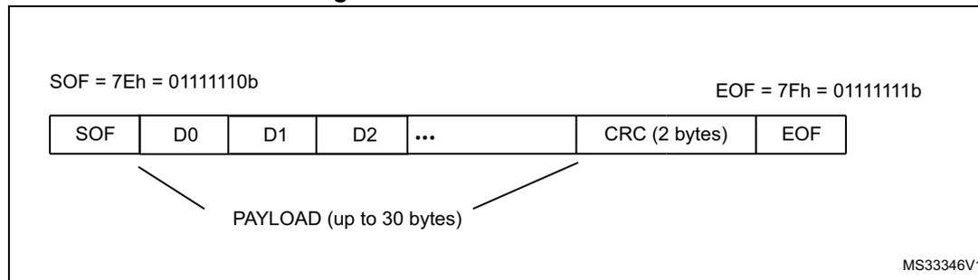
The diagram illustrates the structure of an SWP frame. It consists of several fields: SOF (Start of Frame), a Payload, CRC (Cyclic Redundancy Check), and EOF (End of Frame). The SOF field is defined as 7Eh (01111110b) and the EOF field as 7Fh (01111111b). The Payload is composed of multiple data bytes (D0, D1, D2, ...) and can be up to 30 bytes long. The CRC is a 2-byte field. The fields are arranged in a sequence: SOF, D0, D1, D2, ..., CRC (2 bytes), EOF. A bracket labeled 'PAYLOAD (up to 30 bytes)' spans from the start of D0 to the end of the last data byte before the CRC.
| SOF | D0 | D1 | D2 | ... | CRC (2 bytes) | EOF |
MS33346V1
The SWPMI embeds one 32-bit data register for transmission (SWPMI_TDR), and one 32-bit data register for reception (SWPMI_RDR).
In transmission, the SOF insertion, the CRC calculation and insertion, and the EOF insertion are managed automatically by the SWPMI. The user only has to provide the Payload content and size. A frame transmission starts as soon as data is written into the SWPMI_TDR register. Dedicated flags indicate an empty transmit data register and a complete frame transmission event.
In reception, the SOF deletion, the CRC calculation and checking, and the EOF deletion are managed automatically by the SWPMI. The user only has to read the Payload content and size. Dedicated flags indicate a full receive data register, a complete frame reception and possibly CRC error events.
The stuffing bits insertion (in transmission) and stuffing bits deletion (in reception) are managed automatically by the SWPMI core. These operations are transparent for the user.
58.3.8 Transmission procedure
Before starting any frame transmission, the user must activate the SWP. Refer to Section 58.3.3: SWP initialization and activation .
There are several possible software implementations for a frame transmission: No software buffer mode, Single software buffer mode, and Multi software buffer mode.
The software buffer usage requires the use of a DMA channel to transfer data from the software buffer in the RAM memory to the transmit data register in the SWPMI peripheral.
No software buffer mode
This mode does not require the use of DMA. The SWP frame transmission handling is done by polling status flags in the main loop or inside the SWPMI interrupt routine. There is a 32-bit transmit data register (SWPMI_TDR) in the SWPMI, thus writing to this register will trigger the transmission of up to 4 bytes.
The No software buffer mode is selected by clearing TXDMA bit in the SWPMI_CR register.
The frame transmission is started by the first write to the SWPMI_TDR register. The low significant byte of the first 32-bit word (bits [7:0]) written into the SWPMI_TDR register) indicates the number of data bytes in the payload, and the 3 other bytes of this word must
contain the first 3 bytes of the payload (bits [15:8] contain the first byte of the payload, bits [23:16] the second byte and bits [31:24] the third byte). Then, the following writes to the SWPMI_TDR register will only contain the following payload data bytes, up to 4 for each write.
Note: The low significant byte of the first 32-bit word written into the SWPMI_TDR register is coding the number of data bytes in the payload. This number could be from 1 to 30. Any other value in the low significant byte will be ignored and the transmission will not start.
Writing to the SWPMI_TDR register will induce the following actions:
- • Send the transition sequence and 8 idle bits (RESUME by master) if the SWP bus state is SUSPENDED (this will not happen if the SWP bus state is already ACTIVATED),
- • Send a Start of frame (SOF),
- • Send the payload according to the SWPMI_TRD register content. If the number of bytes in the payload is greater than 3, the SWPMI_TDR needs to be refilled by software, each time the TXE flag in the SWPMI_ISR register is set, and as long as the TXBEF flag is not set in the SWPMI_ISR register,
- • Send the 16-bit CRC, automatically calculated by the SWPMI core,
- • Send an End of frame (EOF).
The TXE flag is cleared automatically when the software is writing to the SWPMI_TDR register.
Once the complete frame is sent, provided that no other frame transmission has been requested (i.e. SWPMI_TDR has not been written again after the TXBEF flag setting), TCF and SUSP flags are set in the SWPMI_ISR register 7 idle bits after the EOF transmission, and an interrupt is generated if TCIE bit is set in the SWPMI_IER register (refer to Figure 719: SWPMI No software buffer mode transmission ).
Figure 719. SWPMI No software buffer mode transmission
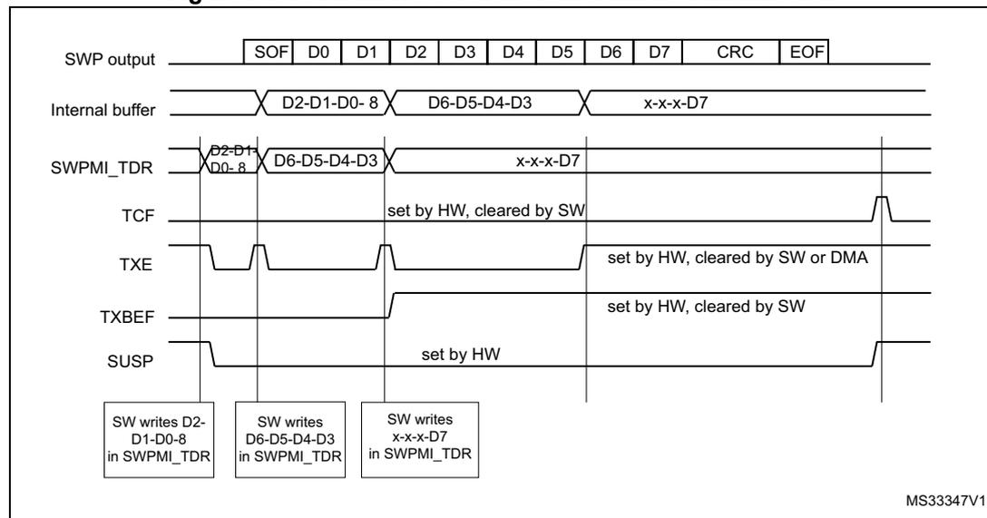
The diagram illustrates the timing and state transitions for an SWPMI transmission without a software buffer. The top row shows the 'SWP output' with a sequence of SOF, data bytes D0 through D7, a CRC, and an EOF. Below it, the 'Internal buffer' is shown with three segments: 'D2-D1-D0-8', 'D6-D5-D4-D3', and 'x-x-x-D7'. The 'SWPMI_TDR' register is shown with the same segments. The 'TCF' flag is set by hardware (HW) and cleared by software (SW). The 'TXE' flag is set by HW and cleared by SW or DMA. The 'TXBEF' flag is set by HW and cleared by SW. The 'SUSP' flag is set by HW. At the bottom, three software write actions are indicated: 'SW writes D2-D1-D0-8 in SWPMI_TDR', 'SW writes D6-D5-D4-D3 in SWPMI_TDR', and 'SW writes x-x-x-D7 in SWPMI_TDR'. The diagram is labeled 'MS33347V1' in the bottom right corner.
If another frame transmission is requested before the end of the EOF transmission, the TCF flag is not set and the frame will be consecutive to the previous one, with only one idle bit in between (refer to Figure 720: SWPMI No software buffer mode transmission, consecutive frames ).
Figure 720. SWPMI No software buffer mode transmission, consecutive frames
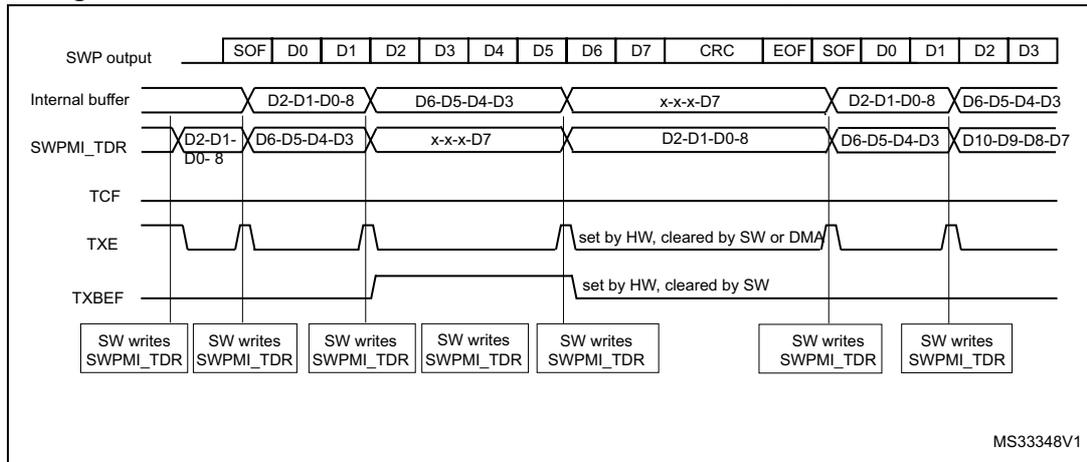
The diagram illustrates the timing and data flow for SWPMI No software buffer mode transmission of consecutive frames. The top row shows the SWP output signal with fields: SOF, D0, D1, D2, D3, D4, D5, D6, D7, CRC, EOF, followed by a second frame starting with SOF, D0, D1, D2, D3. Below this, the Internal buffer is shown with 32-bit words: D2-D1-D0-8, D6-D5-D4-D3, x-x-x-D7, D2-D1-D0-8, D6-D5-D4-D3. The SWPMI_TDR register is shown with 32-bit words: D2-D1-D0-8, D6-D5-D4-D3, x-x-x-D7, D2-D1-D0-8, D6-D5-D4-D3, D10-D9-D8-D7. The TCF flag is shown as a pulse. The TXE flag is shown as a pulse that is set by hardware and cleared by software or DMA. The TXBEF flag is shown as a pulse that is set by hardware and cleared by software. At the bottom, software intervention points are indicated: 'SW writes SWPMI_TDR' for each 32-bit word. The diagram is labeled MS33348V1.
Single software buffer mode
This mode allows to transmit a complete SWP frame without a CPU intervention, using the DMA. The DMA will refill the 32-bit SWPMI_TDR register, and the software can poll the end of the frame transmission using the SWPMI_TXBEF flag.
The Single software buffer mode is selected by setting TXDMA bit and clearing TXMODE bit in the SWPMI_CR register.
The DMA channel or stream must be configured in following mode (refer to DMA section):
- • memory to memory mode disabled,
- • memory increment mode enabled,
- • memory size set to 32-bit,
- • peripheral size set to 32-bit,
- • peripheral increment mode disabled,
- • circular mode disabled,
- • data transfer direction set to read from memory.
- • the number of words to be transferred must be set according to the SWP frame length,
- • the source address is the SWP frame buffer in RAM,
- • the destination address is the SWPMI_TDR register.
Then the user must:
- 1. Set TXDMA bit in the SWPMI_CR register,
- 2. Set TXBEIE bit in the SWPMI_IER register,
- 3. Fill the buffer in the RAM memory (with the number of data bytes in the payload on the least significant byte of the first word),
- 4. Enable stream or channel in DMA module to start DMA transfer and frame transmission.
A DMA request is issued by SWPMI when TXE flag in SWPMI_ISR is set. The TXE flag is cleared automatically when the DMA is writing to the SWPMI_TDR register.
In the SWPMI interrupt routine, the user must check TXBEF bit in the SWPMI_ISR register. If it is set, and if another frame needs to be transmitted, the user must:
- 1. Disable stream or channel in DMA module
- 2. Update the buffer in the RAM memory with the content of the next frame to be sent
- 3. Configure the total number of words to be transferred in DMA module
- 4. Enable stream or channel in DMA module to start next frame transmission
- 5. Set CTXBEF bit in the SWPMI_ICR register to clear the TXBEF flag
Multi software buffer mode
This mode allows to work with several frame buffers in the RAM memory, in order to ensure a continuous transmission, keeping a very low CPU load, and allowing more latency for buffer update by software thanks to the DMA. The software can check the DMA counters at any time and update SWP frames accordingly in the RAM memory.
The Multi software buffer mode must be used in combination with DMA in circular mode.
Each transmission buffer in the RAM memory must have a fixed length of eight 32-bit words, whatever the number of bytes in the SWP frame payload. The transmission buffers in the RAM memory must be filled by the software, keeping an offset of 8 between two consecutive ones. The first data byte of the buffer is the number of bytes of the frame payload. See the buffer example in Figure 721: SWPMI Multi software buffer mode transmission
The Multi software buffer mode is selected by setting both TXDMA and TXMODE bits in SWPMI_CR register.
For example, in order to work with 4 transmission buffers, the user must configure the DMA as follows:
The DMA channel or stream must be configured in following mode (refer to DMA section):
- • memory to memory mode disabled,
- • memory increment mode enabled,
- • memory size set to 32-bit,
- • peripheral size set to 32-bit,
- • peripheral increment mode disabled,
- • circular mode enabled,
- • data transfer direction set to read from memory,
- • the number of words to be transferred must be set to 32 (8 words per buffer),
- • the source address is the buffer1 in RAM,
- • the destination address is the SWPMI_TDR register.
Then, the user must:
- 1. Set TXDMA in the SWPMI_CR register
- 2. Set TXBEIE in the SWPMI_IER register
- 3. Fill buffer1, buffer2, buffer3 and buffer4 in the RAM memory (with the number of data bytes in the payload on the least significant byte of the first word)
- 4. Enable stream or channel in DMA module to start DMA.
In the SWPMI interrupt routine, the user must check TXBEF bit in the SWPMI_ISR register. If it is set, the user must set CTXBEF bit in SWPMI_ICR register to clear TXBEF flag and the user can update buffer1 in the RAM memory.
In the next SWPMI interrupt routine occurrence, the user will update buffer2, and so on.
The Software can also read the DMA counter (number of data to transfer) in the DMA registers in order to retrieve the frame which has already been transferred from the RAM memory and transmitted. For example, if the software works with 4 transmission buffers, and if the DMA counter equals 17, it means that two buffers are ready for updating in the RAM area. This is useful in case several frames are sent before the software can handle the SWPMI interrupt. If this happens, the software will have to update several buffers.
When there are no more frames to transmit, the user must disable the circular mode in the DMA module. The transmission will stop at the end of the buffer4 transmission.
If the transmission needs to stop before (for example at the end of buffer2), the user must set the low significant byte of the first word to 0 in buffer3 and buffer4.
TXDMA bit in the SWPMI_CR register will be cleared by hardware as soon as the number of data bytes in the payload is read as 0 in the least significant byte of the first word.
Figure 721. SWPMI Multi software buffer mode transmission
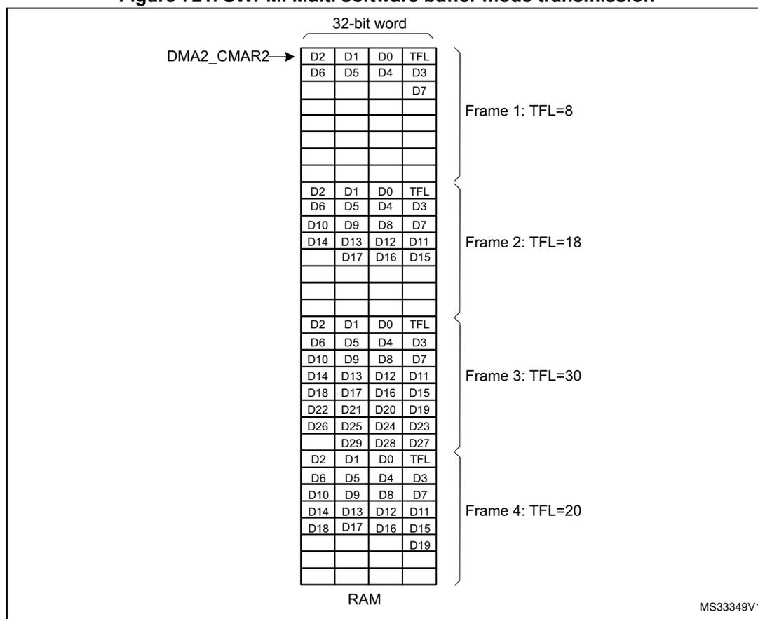
32-bit word
| DMA2_CMAR2 → | D2 | D1 | D0 | TFL | } Frame 1: TFL=8 |
| D6 | D5 | D4 | D3 | ||
| D7 | |||||
| D2 | D1 | D0 | TFL | } Frame 2: TFL=18 | |
| D6 | D5 | D4 | D3 | ||
| D10 | D9 | D8 | D7 | ||
| D14 | D13 | D12 | D11 | ||
| D17 | D16 | D15 | |||
| D2 | D1 | D0 | TFL | } Frame 3: TFL=30 | |
| D6 | D5 | D4 | D3 | ||
| D10 | D9 | D8 | D7 | ||
| D14 | D13 | D12 | D11 | ||
| D18 | D17 | D16 | D15 | ||
| D22 | D21 | D20 | D19 | ||
| D26 | D25 | D24 | D23 | ||
| D29 | D28 | D27 | |||
| D2 | D1 | D0 | TFL | } Frame 4: TFL=20 | |
| D6 | D5 | D4 | D3 | ||
| D10 | D9 | D8 | D7 | ||
| D14 | D13 | D12 | D11 | ||
| D18 | D17 | D16 | D15 | ||
| D19 | |||||
RAM
MS33349V1
58.3.9 Reception procedure
Before starting any frame reception, the user must activate the SWP (refer to Section 58.3.3: SWP initialization and activation ).
Once SWPACT bit is set in the SWPMI_CR register, a RESUME from slave state sets the SRF flag in the SWPMI_ISR register and automatically enables the SWPMI for the frame reception.
If the SWP bus is already in the ACTIVATED state (for example because a frame transmission is ongoing), the SWPMI core does not need any RESUME by slave state, and the reception can take place immediately.
There are several possible software implementations for a frame reception:
- • No software buffer mode,
- • Single software buffer mode,
- • Multi software buffer mode.
The software buffer usage requires the use of a DMA channel to transfer data from the receive data register in the SWPMI peripheral to the software buffer in the RAM memory.
No software buffer mode
This mode does not require the use of DMA. The SWP frame reception handling is done by polling status flags in the main loop or inside the SWPMI interrupt routine. There is a 32-bit receive data register (SWPMI_RDR) in the SWPMI, allowing to receive up to 4 bytes before reading this register.
The No software buffer mode is selected by resetting RXDMA bit in the SWPMI_CR register.
Once a Start of frame (SOF) is received, the following bytes (payload) are stored in the SWPMI_RDR register. Once the SWPMI_RDR is full, the RXNE flag is set in SWPMI_ISR and an interrupt is generated if RIE bit is set in SWPMI_IER register. The user can read the SWPMI_RDR register and the RXNE flag is cleared automatically when the software is reading the SWPMI_RDR register.
Once the complete frame has been received, including the CRC and the End of frame (EOF), both RXNE and RXBFF flags are set in the SWPMI_ISR register. The user must read the last byte(s) of the payload in the SWPMI_RDR register and set CRXBFF flag in SWPMI_ICR in order to clear the RXBFF flag. The number of data bytes in the payload is available in the SWPMI_RFL register. Again, the RXNE flag is reset automatically when the software is reading the SWPMI_RDR register (refer to Figure 722: SWPMI No software buffer mode reception ).
Reading the SWPMI_RDR register while RXNE is cleared will return 0.
Figure 722. SWPMI No software buffer mode reception
The diagram illustrates the reception of an SWP frame without software buffering. The top row shows the incoming SWP input frame: SOF, D0, D1, D2, D3, D4, D5, D6, D7, D8, D9, D10, D11, D12, D13, CRC, EOF. Below it, the internal buffer is shown as a series of 32-bit words: x-x-x-x, D3-D2-D1-D0, D7-D6-D5-D4, D11-D10-D9-D8, x-x-D13-D12. The SWPMI_RDR register is read by software (SW reads SWPMI_RDR) at four points, corresponding to the four 32-bit words in the buffer. The SWPMI_RFL register shows the number of valid data bits (x, 14d). The TCF flag is set by hardware when the frame is complete and cleared by software. The RXNE flag is set by hardware when the buffer is not empty and cleared by software or DMA. The RXBFF flag is set by hardware when the buffer is full and cleared by software. The SUSPEND flag is set by hardware when the RXDMA bit is set in the SWPMI_CR register.
Single software buffer mode
This mode allows to receive a complete SWP frame without any CPU intervention using the DMA. The DMA transfers received data from the 32-bit SWPMI_RDR register to the RAM memory, and the software can poll the end of the frame reception using the SWPMI_RBFF flag.
The Single software buffer mode is selected by setting RXDMA bit and clearing RXMODE bit in the SWPMI_CR register.
The DMA must be configured as follows:
The DMA channel or stream must be configured in following mode (refer to DMA section):
- • memory to memory mode disabled,
- • memory increment mode enabled,
- • memory size set to 32-bit,
- • peripheral size set to 32-bit,
- • peripheral increment mode disabled,
- • circular mode disabled,
- • data transfer direction set to read from peripheral,
- • the number of words to be transferred must be set to 8,
- • the source address is the SWPMI_RDR register,
- • the destination address is the SWP frame buffer in RAM.
Then the user must:
- 1. Set RXDMA bit in the SWPMI_CR register
- 2. Set RXBFIE bit in the SWPMI_IER register
- 3. Enable stream or channel in DMA module.
A DMA request is issued by SWPMI when RXNE flag is set in SWPMI_ISR. The RXNE flag is cleared automatically when the DMA is reading the SWPMI_RDR register.
In the SWPMI interrupt routine, the user must check RXBFF bit in the SWPMI_ISR register. If it is set, the user must:
- 1. Disable stream or channel in DMA module
- 2. Read the number of bytes in the received frame payload in the SWPMI_RFL register
- 3. Read the frame payload in the RAM buffer
- 4. Enable stream or channel in DMA module
- 5. Set CRXBFF bit in the SWPMI_ICR register to clear RXBFF flag (refer to Figure 723: SWPMI single software buffer mode reception ).
Figure 723. SWPMI single software buffer mode reception
The diagram illustrates the timing and data flow for SWPMI single software buffer mode reception. It shows the following signals and their states over time:
- SWP input: Shows a frame structure with SOF, D0-D13, CRC, and EOF. The internal buffer is shown as a circular buffer with segments: x-x-x-x, D3-D2-D1-D0, D7-D6-D5-D4, D11-D10-D9-D8, and x-x-D13-D12.
- SWPMI_RDR: Shows the data being read from the internal buffer. It contains segments: x-x-x-x, D3-D2-D1-D0, D7-D6-D5-D4, D11-D10-D9-D8, and x-x-D13-D12.
- SWPMI_RFL: Shows the receive flag level. It is set by hardware (HW) and cleared by software (SW). The value 14d (decimal 14) is shown at the end of the frame.
- TCF: Set by HW, cleared by SW. It pulses when the frame is complete.
- RXNE: Set by HW, cleared by SW. It pulses when the internal buffer is non-empty.
- RXBFF: Set by HW, cleared by SW. It pulses when the buffer is full.
- SUSPEND: Set by HW. It pulses when the frame is complete.
Below the signals, four DMA transfer boxes indicate that data is transferred from SWPMI_RDR to RAM. The RAM contains the following data segments:
- D3-D2-D1-D0
- D7-D6-D5-D4
- D11-D10-D9-D8
- x-x-D13-D12
MS33351V1
Multi software buffer mode
This mode allows to work with several frame buffers in the RAM memory, in order to ensure a continuous reception, keeping a very low CPU load, using the DMA. The frame payloads are stored in the RAM memory, together with the frame status flags. The software can check the DMA counters and status flags at any time to handle the received SWP frames in the RAM memory.
The Multi software buffer mode must be used in combination with the DMA in circular mode.
The Multi software buffer mode is selected by setting both RXDMA and RXMODE bits in SWPMI_CR register.
In order to work with n reception buffers in RAM, the DMA channel or stream must be configured in following mode (refer to DMA section):
- • memory to memory mode disabled,
- • memory increment mode enabled,
- • memory size set to 32-bit,
- • peripheral size set to 32-bit,
- • peripheral increment mode disabled,
- • circular mode enabled,
- • data transfer direction set to read from peripheral,
- • the number of words to be transferred must be set to \( 8 \times n \) (8 words per buffer),
- • the source address is the SWPMI_TDR register,
- • the destination address is the buffer1 address in RAM
Then the user must:
- 1. Set RXDMA in the SWPMI_CR register
- 2. Set RXBFIE in the SWPMI_IER register
- 3. Enable stream or channel in the DMA module.
In the SWPMI interrupt routine, the user must check RXBFF in the SWPMI_ISR register. If it is set, the user must set CRXBFF bit in the SWPMI_ICR register to clear RXBFF flag and the user can read the first frame payload received in the first buffer (at the RAM address set in DMA2_CMAR1).
The number of data bytes in the payload is available in bits [23:16] of the last 8th word.
In the next SWPMI interrupt routine occurrence, the user will read the second frame received in the second buffer (address set in DMA2_CMAR1 + 8), and so on (refer to Figure 724: SWPMI Multi software buffer mode reception ).
In case the application software cannot ensure to handle the SWPMI interrupt before the next frame reception, each buffer status is available in the most significant byte of the 8th buffer word:
- • The CRC error flag (equivalent to RXBERF flag in the SWPMI_ISR register) is available in bit 24 of the 8th word. Refer to Section 58.3.10: Error management for an CRC error description.
- • The receive overrun flag (equivalent to RXOVRF flag in the SWPMI_ISR register) is available in bit 25 of the 8th word. Refer to Section 58.3.10: Error management for an overrun error description.
- • The receive buffer full flag (equivalent to RXBFF flag in the SWPMI_ISR register) is available in bit 26 of the 8th word.
In case of a CRC error, both RXBFF and RXBERF flags are set, thus bit 24 and bit 26 are set.
In case of an overrun, an overrun flag is set, thus bit 25 is set. The receive buffer full flag is set only in case of an overrun during the last word reception; then, both bit 25 and bit 26 are set for the current and the next frame reception.
The software can also read the DMA counter (number of data to transfer) in the DMA registers in order to retrieve the frame which has already been received and transferred into the RAM memory through DMA. For example, if the software works with 4 reception buffers,
and if the DMA counter equals 17, it means that two buffers are ready for reading in the RAM area.
In Multi software buffer reception mode, if the software is reading bits 24, 25 and 26 of the 8th word, it does not need to clear RXBERF, RXOVRF and RXBFF flags after each frame reception.
Figure 724. SWPMI Multi software buffer mode reception
The diagram illustrates the reception of four frames in SWPMI Multi software buffer mode. The top section shows signal timing for SWP input, SWPMI_RDR (Receive Data Register), SWPMI_RFL (Receive Flag), TCF (Transfer Complete Flag), RXNE (Receive Not Empty), RXBFF (Receive Buffer Full Flag), and SUSPEND. The bottom section shows the RAM buffer structure where data is transferred from SWPMI_RDR to RAM via DMA. The RAM buffer is organized into four frames (Frame1 to Frame4), each containing multiple words. The data is transferred in chunks of 16 bits (D3-D2-D1-D0, D7-D6-D5-D4, D11-D10-D9-D8, D15-D14-D13-D12). The diagram also shows the SWP input sequence: SOF, D0-D13, CRC, EOF, SOF, D0.
58.3.10 Error management
Underrun during payload transmission
During the transmission of the frame payload, a transmit underrun is indicated by the TXUNRF flag in the SWPMI_ISR register. An interrupt is generated if TXBUNREIE bit is set in the SWPMI_IER register.
If a transmit underrun occurs, the SWPMI stops the payload transmission and sends a corrupted CRC (the first bit of the first CRC byte sent is inverted), followed by an EOF. If DMA is used, TXDMA bit in the SWPMI_CR register is automatically cleared.
Any further write to the SWPMI_TDR register while TXUNRF is set will be ignored. The user must set CTXUNRF bit in the SWPMI_ICR register to clear TXUNRF flag.
Overrun during payload reception
During the reception of the frame payload, a receive overrun is indicated by RXOVRF flag in the SWPMI_ISR register. If a receive overrun occurs, the SWPMI does not update SWPMI_RDR with the incoming data. The incoming data will be lost.
The reception carries on up to the EOF and, if the overrun condition disappears, the RXBFF flag is set. When RXBFF flag is set, the user can check the RXOVRF flag. The user must set CRXOVRF bit in the SWPMI_ICR register to clear RXBOVRF flag.
If the user wants to detect the overrun immediately, RXBOVREIE bit in the SWPMI_IER register can be set in order to generate an interrupt as soon as the overrun occurs.
The RXOVRF flag is set at the same time as the RXNE flag, two SWPMI_RDR reads after the overrun event occurred. It indicates that at least one received byte was lost, and the loaded word in SWPMI_RDR contains the bytes received just before the overrun.
In Multi software buffer mode, if RXOVRF flag is set for the last word of the received frame, then the overrun bit (bit 25 of the 8th word) is set for both the current and the next frame.
CRC error during payload reception
Once the two CRC bytes have been received, if the CRC is wrong, the RXBERF flag in the SWPMI_ISR register is set after the EOF reception. An interrupt is generated if RXBEIE bit in the SWPMI_IER register is set (refer to Figure 725: SWPMI single buffer mode reception with CRC error ). The user must set CRXBERF bit in SWPMI_ICR to clear RXBERF flag.
Figure 725. SWPMI single buffer mode reception with CRC error
Missing or corrupted stuffing bit during payload reception
When a stuffing bit is missing or is corrupted in the payload, RXBERF and RXBFF flags are set in SWPMI_ISR after the EOF reception.
Corrupted EOF reception
Once an SOF has been received, the SWPMI accumulates the received bytes until the reception of an EOF (ignoring any possible SOF). Once an EOF has been received, the SWPMI is ready to start a new frame reception and waits for an SOF.
In case of a corrupted EOF, RXBERF and RXBFF flags will be set in the SWPMI_ISR register after the next EOF reception.
Note: In case of a corrupted EOF reception, the payload reception carries on, thus the number of bytes in the payload might get the value 31 if the number of received bytes is greater than 30. The number of bytes in the payload is read in the SWPMI_RFL register or in bits [23:16] of the 8th word of the buffer in the RAM memory, depending on the operating mode.
58.3.11 Loopback mode
The loopback mode can be used for test purposes. The user must set LPBK bit in the SWPMI_CR register in order to enable the loopback mode.
When the loopback mode is enabled, SWPMI_TX and SWPMI_RX signals are connected together. As a consequence, all frames sent by the SWPMI will be received back.
58.4 SWPMI low-power modes
Table 464. Effect of low-power modes on SWPMI
| Mode | Description |
|---|---|
| Sleep | No effect. SWPMI interrupts cause the device to exit the Sleep mode. |
| Stop | A RESUME from SUSPENDED mode issued by the slave can wake up the device from Stop mode if the swpmi_ker_ck is HSI (refer to Section 58.3.1: SWPMI block diagram ). |
| Standby | The SWPMI is stopped. |
58.5 SWPMI interrupts
All SWPMI interrupts are connected to the NVIC.
To enable the SWPMI interrupt, the following sequence is required:
- 1. Configure and enable the SWPMI interrupt channel in the NVIC
- 2. Configure the SWPMI to generate SWPMI interrupts (refer to the SWPMI_IER register).
Table 465. Interrupt control bits
| Interrupt event | Event flag | Enable control bit | Exit the Sleep mode | Exit the Stop mode | Exit the Standby mode |
|---|---|---|---|---|---|
| Receive buffer full | RXBFF | RXBFIE | yes | no | no |
| Transmit buffer empty | TXBEF | TXBEIE | yes | no | no |
| Receive buffer error (CRC error) | RXBERF | RXBEIE | yes | no | no |
| Receive buffer overrun | RXOVRF | RXBOVEREIE | yes | no | no |
| Transmit buffer underrun | TXUNRF | TXBUNREIE | yes | no | no |
| Receive data register not empty | RXNE | RIE | yes | no | no |
| Transmit data register full | TXE | TIE | yes | no | no |
| Transfer complete flag | TCF | TCIE | yes | no | no |
| Slave resume flag | SRF | SRIE | yes | yes (1) | no |
| Transceiver ready flag | RDYF | RDYIE | yes | no | no |
- 1. If HSI is selected for swpmi_ker_ck.
58.6 SWPMI registers
Refer to Section 1.2 of the reference manual for a list of abbreviations used in register descriptions.
The peripheral registers can only be accessed by words (32-bit).
58.6.1 SWPMI configuration/control register (SWPMI_CR)
Address offset: 0x00
Reset value: 0x0000 0000
| 31 | 30 | 29 | 28 | 27 | 26 | 25 | 24 | 23 | 22 | 21 | 20 | 19 | 18 | 17 | 16 |
|---|---|---|---|---|---|---|---|---|---|---|---|---|---|---|---|
| Res. | Res. | Res. | Res. | Res. | Res. | Res. | Res. | Res. | Res. | Res. | Res. | Res. | Res. | Res. | Res. |
| 15 | 14 | 13 | 12 | 11 | 10 | 9 | 8 | 7 | 6 | 5 | 4 | 3 | 2 | 1 | 0 |
| Res. | Res. | Res. | Res. | SWP EN | DEACT | Res. | Res. | Res. | Res. | SWP ACT | LPBK | TXMOD E | RXMO DE | TXDMA | RXDMA |
| rw | rw | rw | rw | rw | rw | rw | rw |
Bits 31:12 Reserved, must be kept at reset value.
Bit 11 SWPTEN : Single wire protocol master transceiver enable
This bit is used to enable the transceiver and control the SWPMI_IO with SWPMI (refer to Section 58.3.3: SWP initialization and activation ).
0: SWPMI_IO pin is controlled by GPIO controller
1: SWPMI_IO transceiver is controlled by SWPMI
Bit 10 DEACT : Single wire protocol master interface deactivate
This bit is used to request the SWP DEACTIVATED state. Setting this bit has the same effect as clearing the SWPACT, except that a possible incoming RESUME by slave will keep the SWP in the ACTIVATED state.
Bits 9:6 Reserved, must be kept at reset value.
Bit 5 SWPACT : Single wire protocol master interface activate
This bit is used to activate the SWP bus (refer to Section 58.3.3: SWP initialization and activation ).
0: SWPMI_IO is pulled down to ground, SWP bus is switched to DEACTIVATED state
1: SWPMI_IO is released, SWP bus is switched to SUSPENDED state
To be able to set SWPACT bit, DEACT bit must have been cleared previously.
Bit 4 LPBK : Loopback mode enable
This bit is used to enable the loopback mode
0: Loopback mode is disabled
1: Loopback mode is enabled
Note: This bit cannot be written while SWPACT bit is set.
Bit 3 TXMODE : Transmission buffering mode
This bit is used to choose the transmission buffering mode. This bit is relevant only when TXDMA bit is set (refer to Table 466: Buffer modes selection for transmission/reception ).
0: SWPMI is configured in Single software buffer mode for transmission
1: SWPMI is configured in Multi software buffer mode for transmission.
Note: This bit cannot be written while SWPACT bit is set.
Bit 2 RXMODE : Reception buffering mode
This bit is used to choose the reception buffering mode. This bit is relevant only when TXDMA bit is set (refer to Table 466: Buffer modes selection for transmission/reception ).
0: SWPMI is configured in Single software buffer mode for reception
1: SWPMI is configured in Multi software buffer mode for reception.
Note: This bit cannot be written while SWPACT bit is set.
Bit 1 TXDMA : Transmission DMA enable
This bit is used to enable the DMA mode in transmission
0: DMA is disabled for transmission
1: DMA is enabled for transmission
Note: TXDMA is automatically cleared if the payload size of the transmitted frame is given as 0x00 (in the least significant byte of TDR for the first word of a frame). TXDMA is also automatically cleared on underrun events (when TXUNRF flag is set in the SWP_ISR register)
Bit 0 RXDMA : Reception DMA enable
This bit is used to enable the DMA mode in reception
0: DMA is disabled for reception
1: DMA is enabled for reception
Table 466. Buffer modes selection for transmission/reception
| Buffer mode | No software buffer | Single software buffer | Multi software buffer |
|---|---|---|---|
| RXMODE/TXMODE | x | 0 | 1 |
| RXDMA/TXDMA | 0 | 1 | 1 |
58.6.2 SWPMI Bitrate register (SWPMI_BRR)
Address offset: 0x04
Reset value: 0x0000 0001
| 31 | 30 | 29 | 28 | 27 | 26 | 25 | 24 | 23 | 22 | 21 | 20 | 19 | 18 | 17 | 16 |
|---|---|---|---|---|---|---|---|---|---|---|---|---|---|---|---|
| Res. | Res. | Res. | Res. | Res. | Res. | Res. | Res. | Res. | Res. | Res. | Res. | Res. | Res. | Res. | Res. |
| 15 | 14 | 13 | 12 | 11 | 10 | 9 | 8 | 7 | 6 | 5 | 4 | 3 | 2 | 1 | 0 |
| Res. | Res. | Res. | Res. | Res. | Res. | Res. | Res. | BR[7:0] | |||||||
| rw | rw | rw | rw | rw | rw | rw | rw | ||||||||
Bits 31:8 Reserved, must be kept at reset value.
Bits 7:0 BR[7:0] : Bitrate prescaler
This field must be programmed to set SWP bus bitrate, taking into account the \( F_{\text{swpmi\_ker\_ck}} \) programmed in the RCC (Reset and Clock Control), according to the following formula:
Note: The programmed bitrate must stay within the following range: from 100 kbit/s up to 2 Mbit/s.
BR[7:0] cannot be written while SWPACT bit is set in the SWPMI_CR register.
58.6.3 SWPMI Interrupt and Status register (SWPMI_ISR)
Address offset: 0x0C
Reset value: 0x0000 02C2
| 31 | 30 | 29 | 28 | 27 | 26 | 25 | 24 | 23 | 22 | 21 | 20 | 19 | 18 | 17 | 16 |
|---|---|---|---|---|---|---|---|---|---|---|---|---|---|---|---|
| Res. | Res. | Res. | Res. | Res. | Res. | Res. | Res. | Res. | Res. | Res. | Res. | Res. | Res. | Res. | Res. |
| 15 | 14 | 13 | 12 | 11 | 10 | 9 | 8 | 7 | 6 | 5 | 4 | 3 | 2 | 1 | 0 |
| Res. | Res. | Res. | Res. | RDYF | DEACTF | SUSP | SRF | TCF | TXE | RXNE | TXUNRF | RXOVR | RXBER | TXBEF | RXBFF |
| r | r | r | r | r | r | r | r | r | r | r | r |
Bits 31:12 Reserved, must be kept at reset value.
Bit 11 RDYF : transceiver ready flag
This bit is set by hardware as soon as transceiver is ready. After setting the SWPTEN bit in SWPMI_CR register to enable the SWPMI_IO transceiver, software must wait for this flag to be set before setting the SWPACT bit to activate the SWP bus.
0: transceiver not ready
1: transceiver ready
Bit 10 DEACTF : DEACTIVATED flag
This bit is a status flag, acknowledging the request to enter the DEACTIVATED mode.
0: SWP bus is in ACTIVATED or SUSPENDED state
1: SWP bus is in DEACTIVATED state
If a RESUME by slave state is detected by the SWPMI while DEACT bit is set by software, the SRF flag will be set, DEACTF will not be set and SWP will move in ACTIVATED state.
Bit 9 SUSP : SUSPEND flag
This bit is a status flag, reporting the SWP bus state
0: SWP bus is in ACTIVATED state
1: SWP bus is in SUSPENDED or DEACTIVATED state
Bit 8 SRF : Slave resume flag
This bit is set by hardware to indicate a RESUME by slave detection. It is cleared by software, writing 1 to CSRF bit in the SWPMI_ICR register.
0: No Resume by slave state detected
1: A Resume by slave state has been detected during the SWP bus SUSPENDED state
Bit 7 TCF : Transfer complete flag
This flag is set by hardware as soon as both transmission and reception are completed and SWP is switched to the SUSPENDED state. It is cleared by software, writing 1 to CTCF bit in the SWPMI_ICR register.
0: Transmission or reception is not completed
1: Both transmission and reception are completed and SWP is switched to the SUSPENDED state
Bit 6 TXE : Transmit data register empty
This flag indicates the transmit data register status
0: Data written in transmit data register SWPMI_TDR is not transmitted yet
1: Data written in transmit data register SWPMI_TDR has been transmitted and SWPMI_TDR can be written to again
Bit 5 RXNE : Receive data register not emptyThis flag indicates the receive data register status
0: Data is not received in the SWPMI_RDR register
1: Received data is ready to be read in the SWPMI_RDR register
Bit 4 TXUNRF : Transmit underrun error flagThis flag is set by hardware to indicate an underrun during the payload transmission i.e. SWPMI_TDR has not been written in time by the software or the DMA. It is cleared by software, writing 1 to the CTXUNRF bit in the SWPMI_ICR register.
0: No underrun error in transmission
1: Underrun error in transmission detected
Bit 3 RXOVR : Receive overrun error flagThis flag is set by hardware to indicate an overrun during the payload reception, i.e. SWPMI_RDR has not be read in time by the software or the DMA. It is cleared by software, writing 1 to CRXOVR bit in the SWPMI_ICR register.
0: No overrun in reception
1: Overrun in reception detected
Bit 2 RXBERF : Receive CRC error flagThis flag is set by hardware to indicate a CRC error in the received frame. It is set synchronously with RXBFF flag. It is cleared by software, writing 1 to CRXBERF bit in the SWPMI_ICR register.
0: No CRC error in reception
1: CRC error in reception detected
Bit 1 TXBEF : Transmit buffer empty flagThis flag is set by hardware to indicate that no more SWPMI_TDR update is required to complete the current frame transmission. It is cleared by software, writing 1 to CTXBEF bit in the SWPMI_ICR register.
0: Frame transmission buffer no yet emptied
1: Frame transmission buffer has been emptied
Bit 0 RXBFF : Receive buffer full flagThis flag is set by hardware when the final word for the frame under reception is available in SWPMI_RDR. It is cleared by software, writing 1 to CRXBFF bit in the SWPMI_ICR register.
0: The last word of the frame under reception has not yet arrived in SWPMI_RDR
1: The last word of the frame under reception has arrived in SWPMI_RDR
58.6.4 SWPMI Interrupt Flag Clear register (SWPMI_ICR)
Address offset: 0x10
Reset value: 0x0000 0000
| 31 | 30 | 29 | 28 | 27 | 26 | 25 | 24 | 23 | 22 | 21 | 20 | 19 | 18 | 17 | 16 |
|---|---|---|---|---|---|---|---|---|---|---|---|---|---|---|---|
| Res. | Res. | Res. | Res. | Res. | Res. | Res. | Res. | Res. | Res. | Res. | Res. | Res. | Res. | Res. | Res. |
| 15 | 14 | 13 | 12 | 11 | 10 | 9 | 8 | 7 | 6 | 5 | 4 | 3 | 2 | 1 | 0 |
| Res. | Res. | Res. | Res. | CRDY F | Res. | Res. | CSRF | CTCF | Res. | Res. | CTXUN RF | CRXOV RF | CRXBER F | CTXBE F | CRXBF F |
| rc_w1 | rc_w1 | rc_w1 | rc_w1 | rc_w1 | rc_w1 | rc_w1 | rc_w1 |
Bits 31:12 Reserved, must be kept at reset value.
Bit 11
CRDYF
: Clear transceiver ready flag
Writing 1 to this bit clears the RDYF flag in the SWPMI_ISR register
Writing 0 to this bit does not have any effect
Bits 10:9 Reserved, must be kept at reset value.
Bit 8
CSRF
: Clear slave resume flag
Writing 1 to this bit clears the SRF flag in the SWPMI_ISR register
Writing 0 to this bit does not have any effect
Bit 7
CTCF
: Clear transfer complete flag
Writing 1 to this bit clears the TCF flag in the SWPMI_ISR register
Writing 0 to this bit does not have any effect
Bits 6:5 Reserved, must be kept at reset value.
Bit 4
CTXUNRF
: Clear transmit underrun error flag
Writing 1 to this bit clears the TXUNRF flag in the SWPMI_ISR register
Writing 0 to this bit does not have any effect
Bit 3
CRXOVRF
: Clear receive overrun error flag
Writing 1 to this bit clears the RXBOCREF flag in the SWPMI_ISR register
Writing 0 to this bit does not have any effect
Bit 2
CRXBERF
: Clear receive CRC error flag
Writing 1 to this bit clears the RXBERF flag in the SWPMI_ISR register
Writing 0 to this bit does not have any effect
Bit 1
CTXBEF
: Clear transmit buffer empty flag
Writing 1 to this bit clears the TXBEF flag in the SWPMI_ISR register
Writing 0 to this bit does not have any effect
Bit 0
CRXBFF
: Clear receive buffer full flag
Writing 1 to this bit clears the RXBFF flag in the SWPMI_ISR register
Writing 0 to this bit does not have any effect
58.6.5 SWPMI Interrupt Enable register (SWPMI_IER)
Address offset: 0x14
Reset value: 0x0000 0000
| 31 | 30 | 29 | 28 | 27 | 26 | 25 | 24 | 23 | 22 | 21 | 20 | 19 | 18 | 17 | 16 |
|---|---|---|---|---|---|---|---|---|---|---|---|---|---|---|---|
| Res. | Res. | Res. | Res. | Res. | Res. | Res. | Res. | Res. | Res. | Res. | Res. | Res. | Res. | Res. | Res. |
| 15 | 14 | 13 | 12 | 11 | 10 | 9 | 8 | 7 | 6 | 5 | 4 | 3 | 2 | 1 | 0 |
| Res. | Res. | Res. | Res. | RDYIE | Res. | Res. | SRIE | TCIE | TIE | RIE | TXUNREIE | RXOVREIE | RXBEIE | TXBEIE | RXBFIE |
| rw | rw | rw | rw | rw | rw | rw | rw | rw | rw | ||||||
Bits 31:12 Reserved, must be kept at reset value.
Bit 11 RDYIE : Transceiver ready interrupt enable
0: Interrupt is inhibited
1: A SWPMI interrupt is generated whenever RDYF flag is set in the SWPMI_ISR register
Bits 10:9 Reserved, must be kept at reset value.
Bit 8 SRIE : Slave resume interrupt enable
0: Interrupt is inhibited
1: An SWPMI interrupt is generated whenever SRF flag is set in the SWPMI_ISR register
Bit 7 TCIE : Transmit complete interrupt enable
0: Interrupt is inhibited
1: An SWPMI interrupt is generated whenever TCF flag is set in the SWPMI_ISR register
Bit 6 TIE : Transmit interrupt enable
0: Interrupt is inhibited
1: An SWPMI interrupt is generated whenever TXE flag is set in the SWPMI_ISR register
Bit 5 RIE : Receive interrupt enable
0: Interrupt is inhibited
1: An SWPMI interrupt is generated whenever RXNE flag is set in the SWPMI_ISR register
Bit 4 TXUNRIE : Transmit underrun error interrupt enable
0: Interrupt is inhibited
1: An SWPMI interrupt is generated whenever TXBUNRF flag is set in the SWPMI_ISR register
Bit 3 RXOVRIE : Receive overrun error interrupt enable
0: Interrupt is inhibited
1: An SWPMI interrupt is generated whenever RXBOVRF flag is set in the SWPMI_ISR register
Bit 2 RXBERIE : Receive CRC error interrupt enable
0: Interrupt is inhibited
1: An SWPMI interrupt is generated whenever RXBERF flag is set in the SWPMI_ISR register
Bit 1 TXBEIE : Transmit buffer empty interrupt enable
0: Interrupt is inhibited
1: An SWPMI interrupt is generated whenever TXBEF flag is set in the SWPMI_ISR register
Bit 0 RXBFIE : Receive buffer full interrupt enable
0: Interrupt is inhibited
1: An SWPMI interrupt is generated whenever RXBFF flag is set in the SWPMI_ISR register
58.6.6 SWPMI Receive Frame Length register (SWPMI_RFL)
Address offset: 0x18
Reset value: 0x0000 0000
| 31 | 30 | 29 | 28 | 27 | 26 | 25 | 24 | 23 | 22 | 21 | 20 | 19 | 18 | 17 | 16 |
|---|---|---|---|---|---|---|---|---|---|---|---|---|---|---|---|
| Res. | Res. | Res. | Res. | Res. | Res. | Res. | Res. | Res. | Res. | Res. | Res. | Res. | Res. | Res. | Res. |
| 15 | 14 | 13 | 12 | 11 | 10 | 9 | 8 | 7 | 6 | 5 | 4 | 3 | 2 | 1 | 0 |
| Res. | Res. | Res. | Res. | Res. | Res. | Res. | Res. | Res. | Res. | Res. | RFL[4:0] | ||||
| r | r | r | r | r | |||||||||||
Bits 31:5 Reserved, must be kept at reset value.
Bits 4:0 RFL[4:0] : Receive frame length
RFL[4:0] is the number of data bytes in the payload of the received frame. The two least significant bits RFL[1:0] give the number of relevant bytes for the last SWPMI_RDR register read.
58.6.7 SWPMI Transmit data register (SWPMI_TDR)
Address offset: 0x1C
Reset value: 0x0000 0000
| 31 | 30 | 29 | 28 | 27 | 26 | 25 | 24 | 23 | 22 | 21 | 20 | 19 | 18 | 17 | 16 |
|---|---|---|---|---|---|---|---|---|---|---|---|---|---|---|---|
| TD[31:16] | |||||||||||||||
| w | w | w | w | w | w | w | w | w | w | w | w | w | w | w | w |
| 15 | 14 | 13 | 12 | 11 | 10 | 9 | 8 | 7 | 6 | 5 | 4 | 3 | 2 | 1 | 0 |
| TD[15:0] | |||||||||||||||
| w | w | w | w | w | w | w | w | w | w | w | w | w | w | w | w |
Bits 31:0 TD[31:0] : Transmit data
Contains the data to be transmitted.
Writing to this register triggers the SOF transmission or the next payload data transmission, and clears the TXE flag.
58.6.8 SWPMI Receive data register (SWPMI_RDR)
Address offset: 0x20
Reset value: 0x0000 0000
| 31 | 30 | 29 | 28 | 27 | 26 | 25 | 24 | 23 | 22 | 21 | 20 | 19 | 18 | 17 | 16 |
|---|---|---|---|---|---|---|---|---|---|---|---|---|---|---|---|
| RD[31:16] | |||||||||||||||
| r | r | r | r | r | r | r | r | r | r | r | r | r | r | r | r |
| 15 | 14 | 13 | 12 | 11 | 10 | 9 | 8 | 7 | 6 | 5 | 4 | 3 | 2 | 1 | 0 |
| RD[15:0] | |||||||||||||||
| r | r | r | r | r | r | r | r | r | r | r | r | r | r | r | r |
Bits 31:0 RD[31:0] : received data
Contains the received data
Reading this register is clearing the RXNE flag.
58.6.9 SWPMI Option register (SWPMI_OR)
Address offset: 0x24
Reset value: 0x0000 0000
| 31 | 30 | 29 | 28 | 27 | 26 | 25 | 24 | 23 | 22 | 21 | 20 | 19 | 18 | 17 | 16 |
|---|---|---|---|---|---|---|---|---|---|---|---|---|---|---|---|
| Res. | Res. | Res. | Res. | Res. | Res. | Res. | Res. | Res. | Res. | Res. | Res. | Res. | Res. | Res. | Res. |
| 15 | 14 | 13 | 12 | 11 | 10 | 9 | 8 | 7 | 6 | 5 | 4 | 3 | 2 | 1 | 0 |
| SWP_ CLASS | SWP_ TBYP | ||||||||||||||
| rw | rw | ||||||||||||||
Bits 31:2 Reserved, must be kept at reset value
Bit 1 SWP_CLASS : SWP class selection
This bit is used to select the SWP class (refer to Section 58.3.3: SWP initialization and activation ).
- 0: Class C: SWPMI_IO uses directly VDD voltage to operate in class C.
This configuration must be selected when VDD is in the range [1.62 V to 1.98 V] - 1: Class B: SWPMI_IO uses an internal voltage regulator to operate in class B.
This configuration must be selected when VDD is in the range [2.70 V to 3.30 V]
Bit 0 SWP_TBYP : SWP transceiver bypass
This bit is used to bypass the internal transceiver (SWPMI_IO), and connect an external transceiver.
- 0: Internal transceiver is enabled. The external interface for SWPMI is SWPMI_IO (SWPMI_RX, SWPMI_TX and SWPMI_SUSPEND signals are not available on GPIOs)
- 1: Internal transceiver is disabled. SWPMI_RX, SWPMI_TX and SWPMI_SUSPEND signals are available as alternate function on GPIOs. This configuration is selected to connect an external transceiver
58.6.10 SWPMI register map and reset value table
Table 467. SWPMI register map and reset values
| Offset | Register name | 31 | 30 | 29 | 28 | 27 | 26 | 25 | 24 | 23 | 22 | 21 | 20 | 19 | 18 | 17 | 16 | 15 | 14 | 13 | 12 | 11 | 10 | 9 | 8 | 7 | 6 | 5 | 4 | 3 | 2 | 1 | 0 |
|---|---|---|---|---|---|---|---|---|---|---|---|---|---|---|---|---|---|---|---|---|---|---|---|---|---|---|---|---|---|---|---|---|---|
| 0x00 | SWPMI_CR | Res. | Res. | Res. | Res. | Res. | Res. | Res. | Res. | Res. | Res. | Res. | Res. | Res. | Res. | Res. | Res. | Res. | Res. | Res. | Res. | SWPTEN | DEACT | Res. | Res. | Res. | Res. | SWPACT | LPBK | TXMODE | RXMODE | TXDMA | RXDMA |
| Reset value | 0 | 0 | 0 | 0 | 0 | 0 | 0 | 0 | |||||||||||||||||||||||||
| 0x04 | SWPMI_BRR | Res. | Res. | Res. | Res. | Res. | Res. | Res. | Res. | Res. | Res. | Res. | Res. | Res. | Res. | Res. | Res. | Res. | Res. | Res. | Res. | Res. | Res. | Res. | Res. | Res. | BRR[7:0] | ||||||
| Reset value | 0 | 0 | 0 | 0 | 0 | 1 | |||||||||||||||||||||||||||
| 0x08 | RESERVED | Res. | Res. | Res. | Res. | Res. | Res. | Res. | Res. | Res. | Res. | Res. | Res. | Res. | Res. | Res. | Res. | Res. | Res. | Res. | Res. | Res. | Res. | Res. | Res. | Res. | Res. | Res. | Res. | Res. | Res. | Res. | Res. |
| Reset value | |||||||||||||||||||||||||||||||||
| 0x0C | SWPMI_ISR | Res. | Res. | Res. | Res. | Res. | Res. | Res. | Res. | Res. | Res. | Res. | Res. | Res. | Res. | Res. | Res. | Res. | Res. | Res. | Res. | RDYF | DEACTF | SUSP | SRF | TCF | TXE | RXNE | TXUNRF | RXOVRF | RXBERF | TXBEF | RXBFF |
| Reset value | 0 | 0 | 1 | 0 | 1 | 1 | 0 | 0 | 0 | 0 | 1 | 0 | |||||||||||||||||||||
| 0x10 | SWPMI_ICR | Res. | Res. | Res. | Res. | Res. | Res. | Res. | Res. | Res. | Res. | Res. | Res. | Res. | Res. | Res. | Res. | Res. | Res. | Res. | Res. | CRDYF | Res. | Res. | CSRF | CTCF | Res. | Res. | CTXUNRF | CRXOVRF | CRXBERF | CTXBEF | CRXBFF |
| Reset value | 0 | 0 | 0 | 0 | 0 | 0 | 0 | 0 | |||||||||||||||||||||||||
| 0x14 | SWPMI_IER | Res. | Res. | Res. | Res. | Res. | Res. | Res. | Res. | Res. | Res. | Res. | Res. | Res. | Res. | Res. | Res. | Res. | Res. | Res. | Res. | RDYIE | Res. | Res. | SRIE | TCIE | TIE | RIE | TXUNRIE | RXOVRIE | RXBERIE | TXBEIE | RXBIE |
| Reset value | 0 | 0 | 0 | 0 | 0 | 0 | 0 | 0 | 0 | 0 | |||||||||||||||||||||||
| 0x18 | SWPMI_RFL | Res. | Res. | Res. | Res. | Res. | Res. | Res. | Res. | Res. | Res. | Res. | Res. | Res. | Res. | Res. | Res. | Res. | Res. | Res. | Res. | Res. | Res. | Res. | Res. | Res. | Res. | RFL[4:0] | |||||
| Reset value | 0 | 0 | 0 | 0 | 0 | ||||||||||||||||||||||||||||
| 0x1C | SWPMI_TDR | TD[31:0] | |||||||||||||||||||||||||||||||
| Reset value | 0 | 0 | 0 | 0 | 0 | 0 | 0 | 0 | 0 | 0 | 0 | 0 | 0 | 0 | 0 | 0 | 0 | 0 | 0 | 0 | 0 | 0 | 0 | 0 | 0 | 0 | 0 | 0 | 0 | 0 | 0 | 0 | |
| 0x20 | SWPMI_RDR | RD[31:0] | |||||||||||||||||||||||||||||||
| Reset value | 0 | 0 | 0 | 0 | 0 | 0 | 0 | 0 | 0 | 0 | 0 | 0 | 0 | 0 | 0 | 0 | 0 | 0 | 0 | 0 | 0 | 0 | 0 | 0 | 0 | 0 | 0 | 0 | 0 | 0 | 0 | 0 | |
| 0x24 | SWPMI_OR | Res. | Res. | Res. | Res. | Res. | Res. | Res. | Res. | Res. | Res. | Res. | Res. | Res. | Res. | Res. | Res. | Res. | Res. | Res. | Res. | Res. | Res. | Res. | Res. | Res. | Res. | Res. | Res. | Res. | Res. | SWP_CLASS | SWP_TBYP |
| Reset value | 0 | 0 | |||||||||||||||||||||||||||||||
Refer to Section 2.3 on page 131 for the register boundary addresses.