57. SPDIF receiver interface (SPDIFRX)
57.1 SPDIFRX interface introduction
The SPDIFRX interface handles S/PDIF audio protocol.
57.2 SPDIFRX main features
- • Up to 4 inputs available
- • Automatic symbol rate detection
- • Maximum symbol rate: 12.288 MHz
- • Stereo stream from 8 to 192 kHz (a) supported
- • Supports audio IEC-60958 and IEC-61937, consumer applications
- • Parity bit management
- • Communication using DMA for audio samples
- • Communication using DMA for control and user channel information
- • Interrupt capabilities
57.3 SPDIFRX functional description
The SPDIFRX peripheral, is designed to receive an S/PDIF flow compliant with IEC-60958 and IEC-61937. These standards support simple stereo streams up to high sample rate, and compressed multi-channel surround sound, such as those defined by Dolby or DTS.
The receiver provides all the necessary features to detect the symbol rate, and decode the incoming data. It is possible to use a dedicated path for the user and channel information in order to ease the interface handling. Figure 698 shows a simplified block diagram.
The SPDIFRX_DC block is responsible of the decoding of the S/PDIF stream received from SPDIFRX_IN[4:1] inputs. This block re-sample the incoming signal, decode the manchester stream, recognize frames, sub-frames and blocks elements. It delivers to the REG_IF part, decoded data, and associated status flags.
This peripheral can be fully controlled via the APB1 bus, and can handle two DMA channels:
- • A DMA channel dedicated to the transfer of audio samples
- • A DMA channel dedicated to the transfer of IEC60958 channel status and user information
Interrupt services are also available either as an alternative function to the DMA, or for signaling error or key status of the peripheral.
The SPDIFRX also offers a signal named spdifrx_frame_sync , which toggles every time that a sub-frame's preamble is detected. So the duty cycle is 50%, and the frequency equal to the frame rate.
This signal can be connected to timer events, in order to compute frequency drift.
a. Check the RCC capabilities in order to verify which sampling rates can be supported.
In addition the SPDIFRX also provides a signal named spdifrx_symb_ck toggling at the symbol rate.
Figure 698. SPDIFRX block diagram
![Figure 698. SPDIFRX block diagram. The diagram shows the internal architecture of the SPDIFRX block. On the left, external pins are shown: spdifrx_ker_ck (input), spdifrx_pclk (input), spdifrx_it (output), spdifrx_dat_dma (input/output), and spdifrx_ctrl_dma (input/output). A 32-bit APB bus connects to the Register interface. The Register interface contains several registers: SPDIFRX_FMTx_DR, SPDIFRX_CR, SPDIFRX_IMR, SPDIFRX_CSR, SPDIFRX_SR, SPDIFRX_IFCR, and SPDIFRX_DIR. These are connected to a 'data' bus and a 'ctrl ch.' bus. Below the registers are the IRQ interface and DMA interface. The SPDIFRX_DC (Data Channel) block contains a RX_BUF 32 bits, SPDIFRX_SEQ (SPDIF data packing and sequencer), SPDIFRX_DEC (Biphase and transition decoder), and SPDIFRX_FE (Re-sync & Edge detection). The SPDIFRX_IN[x], SPDIFRX_IN[x+1], ..., SPDIFRX_IN[x+n] (1) pins are connected to the SPDIFRX_FE block. The SPDIFRX_FE block also outputs spdifrx_symb_ck and spdifrx_frame_sync. The diagram is divided into two clock domains: spdifrx_pclk clock domain and spdif_ker_ck clock domain.](/RM0468-STM32H723-733-725-735-730/3c44cbbcbe321eaefd4f3bb87a31ed68_img.jpg)
1. 'n' is fixed to 4, and 'x' is set to 1.
57.3.1 SPDIFRX pins and internal signals
Table 455 lists the SPDIFRX internal input/output signals, Table 456 the SPDIFRX pins (alternate functions).
Table 455. SPDIFRX internal input/output signals
| Signal name | Signal type | Description |
|---|---|---|
| spdifrx_ker_ck | Digital input | SPDIFRX kernel clock |
| spdifrx_pclk | Digital input | SPDIFRX register interface clock |
| spdifrx_it | Digital output | SPDIFRX global interrupt |
| spdifrx_dat_dma | Digital input/output | SPDIFRX DMA request (and acknowledge) for data transfer |
| spdifrx_ctrl_dma | Digital input/output | SPDIFRX DMA request (and acknowledge) for channel status and user information transfer |
| spdifrx_frame_sync | Digital output | SPDIFRX frame rate synchronization signal |
| spdifrx_symb_ck | Digital output | SPDIFRX channel symbol clock |
Table 456. SPDIFRX pins
| Signal name | Signal type | Description |
|---|---|---|
| SPDIFRX_IN1 | Digital input | Input 1 for S/PDIF signal |
| SPDIFRX_IN2 | Digital input | Input 2 for S/PDIF signal |
| SPDIFRX_IN3 | Digital input | Input 3 for S/PDIF signal |
| SPDIFRX_IN4 | Digital input | Input 4 for S/PDIF signal |
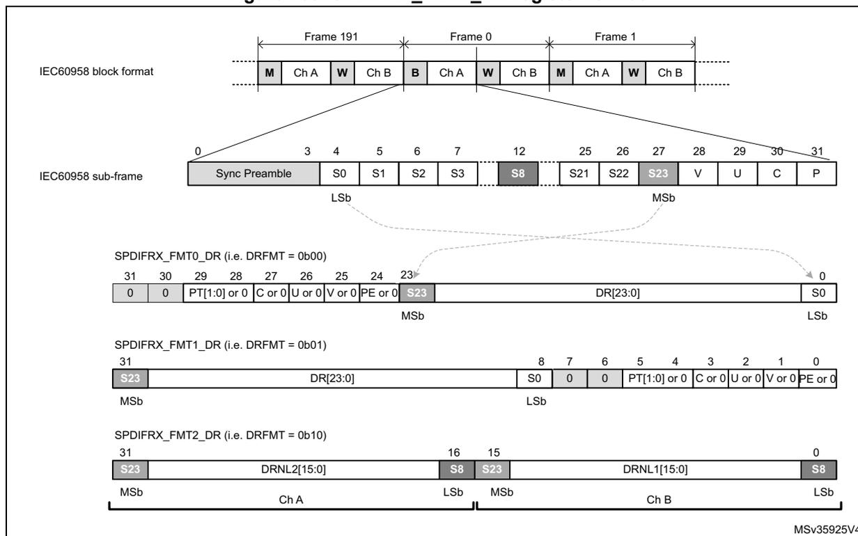
57.3.2 S/PDIF protocol (IEC-60958)
S/PDIF block
A S/PDIF frame is composed of two sub-frames (see Figure 699 ). Each sub-frame contains 32 bits (or time slots):
- • Bits 0 to 3 carry one of the synchronization preambles
- • Bits 4 to 27 carry the audio sample word in linear 2's complement representation. The most significant bit (MSB) is carried by bit 27. When a 20-bit coding range is used, bits 8 to 27 carry the audio sample word with the LSB in bit 8.
- • Bit 28 (validity bit “V”) indicates if the data is valid (for converting it to analog for example)
- • Bit 29 (user data bit “U”) carries the user data information like the number of tracks of a Compact Disk.
- • Bit 30 (channel status bit “C”) carries the channel status information like sample rate and protection against copy.
- • Bit 31 (parity bit “P”) carries a parity bit such that bits 4 to 31 inclusive carry an even number of ones and an even number of zeroes (even parity).
Figure 699. S/PDIF sub-frame format
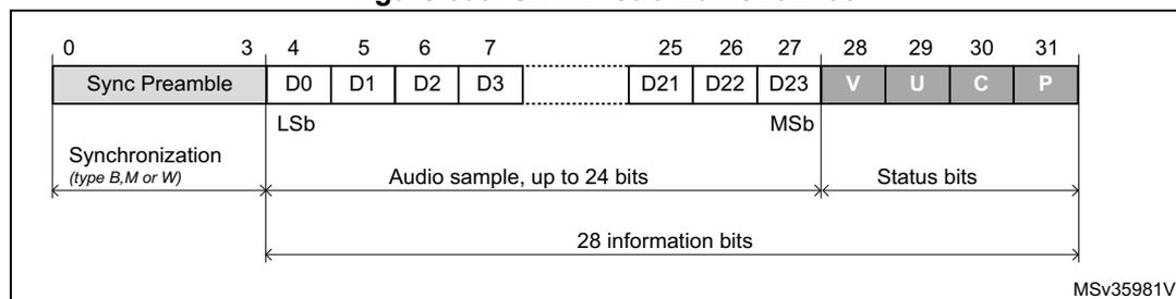
| 0 | 3 | 4 | 5 | 6 | 7 | ... | 25 | 26 | 27 | 28 | 29 | 30 | 31 | ||||
| Sync Preamble | D0 | D1 | D2 | D3 | ... | D21 | D22 | D23 | V | U | C | P | |||||
| Synchronization (type B,M or W) | Audio sample, up to 24 bits | Status bits | |||||||||||||||
| 28 information bits | |||||||||||||||||
MSV35981V1
For linear coded audio applications, the first sub-frame (left or “A” channel in stereophonic operation and primary channel in monophonic operation) normally starts with preamble “M”. However, the preamble changes to preamble “B” once every 192 frames to identify the start of the block structure used to organize the channel status and user information. The second sub-frame (right or “B” channel in stereophonic operation and secondary channel in monophonic operation) always starts with preamble “W”.
A S/PDIF block contains 192 pairs of sub-frames of 32 bits.
Figure 700. S/PDIF block format
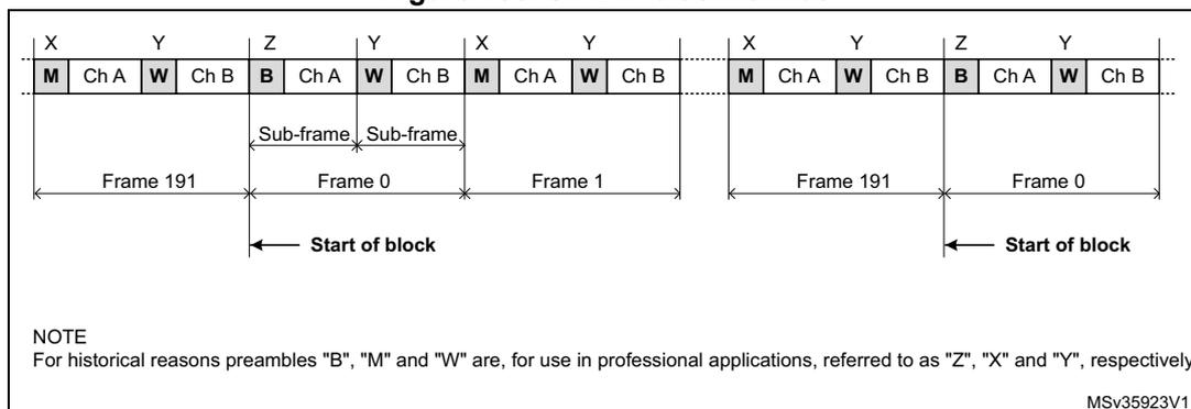
The diagram illustrates the S/PDIF block format. It shows a sequence of sub-frames and preambles. Each sub-frame consists of four fields: X (M), Y (Ch A), Z (W), and Y (Ch B). The sequence of sub-frames is: Frame 191, Frame 0, Frame 1, Frame 191, Frame 0. The 'Start of block' is indicated by an arrow pointing to the beginning of Frame 0 in both instances. A note at the bottom states: 'NOTE: For historical reasons preambles "B", "M" and "W" are, for use in professional applications, referred to as "Z", "X" and "Y", respectively.' The code MSv35923V1 is shown in the bottom right corner.
Synchronization preambles
The preambles patterns are inverted or not according to the previous half-bit value. This previous half-bit value is the level of the line before enabling a transfer for the first "B" preamble of the first frame. For the others preambles, this previous half-bit value is the second half-bit of the parity bit of the previous sub-frame. The preambles patterns B, M and W are described in the Figure 701 .
Figure 701. S/PDIF Preambles
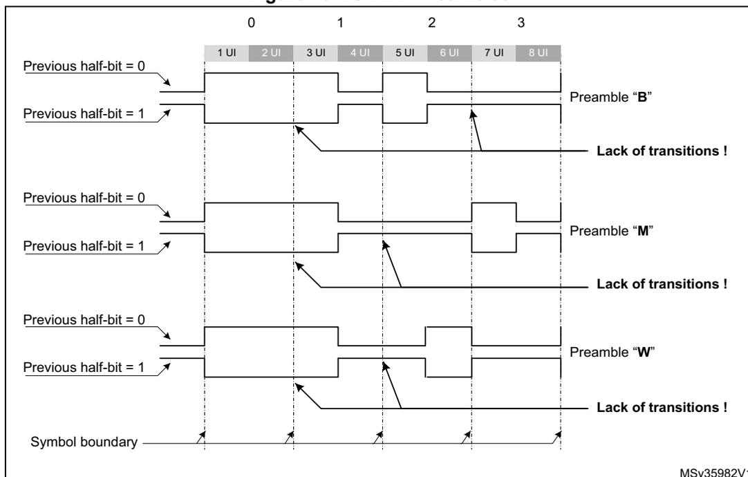
The diagram shows the timing and signal levels for preambles B, M, and W. It is divided into four horizontal sections. The top section shows the timing for Preamble "B" with two signal levels: 'Previous half-bit = 0' and 'Previous half-bit = 1'. The second section shows the timing for Preamble "M" with the same two signal levels. The third section shows the timing for Preamble "W" with the same two signal levels. The bottom section shows the 'Symbol boundary' for each of the four sections. The signal levels are represented by horizontal lines with vertical transitions. The text 'Lack of transitions !' is placed next to the signal levels for Preamble "B", "M", and "W" when the previous half-bit is 1. The code MSv35982V1 is shown in the bottom right corner.
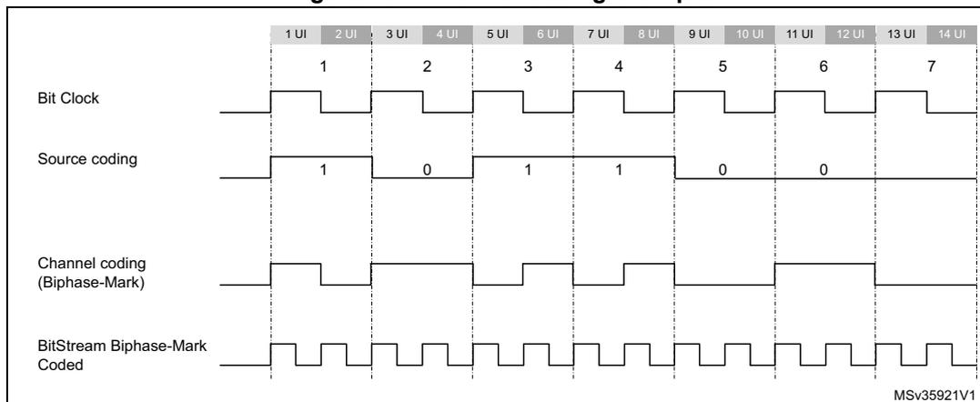
Coding of information bits
In order to minimize the DC component value on the transmission line, and to facilitate clock recovery from the data stream, bits 4 to 31 are encoded in biphase-mark.
Each bit to be transmitted is represented by a symbol comprising two consecutive binary states. The first state of a symbol is always different from the second state of the previous symbol. The second state of the symbol is identical to the first if the bit to be transmitted is
logical 0. However, it is different if the bit is logical 1. These states are named “UI” (unit interval) in the IEC-60958 specification.
The 24 data bits are transferred LSB first.
Figure 702. Channel coding example
57.3.3 SPDIFRX decoder (SPDIFRX_DC)
Main principle
The technique used by the SPDIFRX in order to decode the S/PDIF stream is based on the measurement of the time interval between two consecutive edges. Three kinds of time intervals may be found into an S/PDIF stream:
- • The long time interval, having a duration of 3 x UI, noted TL. It appears only during preambles.
- • The medium time interval, having a duration of 2 x UI, noted TM. It appears both in some preambles or into the information field.
- • The short time interval, having a duration of 1 x UI, noted TS. It appears both in some preambles or into the information field.
The SPDIFRX_DC block is responsible of the decoding of the received S/PDIF stream. It takes care of the following functions:
- • Resampling and filtering of the incoming signal
- • Estimation of the time-intervals
- • Estimation of the symbol rate and synchronization
- • Decoding of the serial data, and check of integrity
- • Detection of the block, and sub-frame preambles
- • Continuous tracking of the symbol rate
Figure 703 gives a detailed view of the SPDIFRX decoder.
Figure 703. SPDIFRX decoder
The diagram shows the internal architecture of the SPDIFRX_DC block. It starts with SPDIFRX_IN[x] and SPDIFRX_IN[x+n] inputs entering an SPDIFRX_FE block for noise filtering & edge detection. The output of the FE block enters the SPDIFRX_DEC block. Inside SPDIFRX_DEC, the signal goes through a 'Longest & shortest transition detector' which outputs MAX_CNT and MIN_CNT. These are followed by a 'Transition coder & Preamble detector' which outputs transition_info and preamble_info. These signals then enter a 'Biphase decoder' which outputs data. The SPDIFRX_DEC block also receives transition_pulse, transition_width_count (13 bits), WIDTH24, and WIDTH40 as inputs. The data from the Biphase decoder goes to a 'Data Packing' block, which also receives data_valid and data. The output of Data Packing goes to an RX_BUF block. The RX_BUF block outputs data and ctrl_ch. A SYNC block is connected to the RX_BUF block. The SPDIFRX_SEQ block contains a TRCNT (13 bits) which receives transition_pulse and spdifrx_ker_ck. The TRCNT output goes to the Data Packing block. A FINE SYNC block is also connected to the Data Packing block.
- 1. 'n' is fixed to 4, and 'x' is set to 1.
Noise filtering and rising/falling edge detection
The S/PDIF signal received on the selected SPDIFRX_IN is re-sampled using the spdifrx_ker_ck clock (acquisition clock). A simple filtering is applied in order to cancel spurs. This is performed by the stage detecting the edge transitions. The edge transitions are detected as follows:
- • A rising edge is detected when the sequence 0 followed by two 1 is sampled.
- • A falling edge is detected when the sequence 1 followed by two 0 is sampled.
- • After a rising edge, a falling edge sequence is expected.
- • After a falling edge, a rising edge sequence is expected.
Figure 704. Noise filtering and edge detection
Timing diagram showing the relationship between SPDIFRX_IN[x], spdifrx_ker_ck, resampled input, filtered input, and transition_pulse. It illustrates four states (S1, S2, S3, S4). A 'Glitch !!' is shown in the SPDIFRX_IN[x] signal between S2 and S3, which is filtered out in the 'filtered input' signal. The 'resampled input' shows bit sequences like '0 1 1', '1 1 1', '1 0 0', '0 1 1', '1 0 1', '1 1 1', '1 0 0', '0 0 1', '1 1 1', '1 0 0', '1 1 1', '1 1 1'. Transition pulses are generated at the detected edges of the filtered input.
Longest and shortest transition detector
The longest and shortest transition detector block detects the maximum (MAX_CNT) and minimum (MIN_CNT) duration between two transitions. The TRCNT counter is used to measure the time interval duration. It is clocked by the spdifrx_ker_ck signal. On every transition pulse, the counter value is stored and the counter is reset to start counting again.
The maximum duration is normally found during the preamble period. This maximum duration is sent out as MAX_CNT. The minimum duration is sent out as MIN_CNT.
The search of the longest and shortest transition is stopped when the transition timer expires. The transition timer is like a watchdog timer that generates a trigger after 70 transitions of the incoming signal. Note that counting 70 transitions insures a delay a bit longer than a sub-frame.
Note that when the TRCNT overflows due to a too long time interval between two pulses, the SPDIFRX is stopped and the flag TERR of SPDIFRX_SR register is set to 1.
Transition coder and preamble detector
The transition coder and preamble detector block receives the MAX_CNT and MIN_CNT. It also receives the current transition width from the TRCNT counter (see Figure 703 ). This block encodes the current transition width by comparing the current transition width with two different thresholds, names TH HI and TH LO .
- • If the current transition width is less than (TH LO - 1), then the data received is half part of data bit '1', and is coded as TS.
- • If the current transition width is greater than (TH LO - 1), and less than TH HI , then the data received is data bit '0', and is coded as TM.
- • If the current transition width is greater than TH HI , then the data received is the long pulse of preambles, and is coded as TL.
- • Else an error code is generated (FERR flag is set).
The thresholds TH HI and TH LO are elaborated using two different methods.
If the peripheral is doing its initial synchronization ('coarse synchronization'), then the thresholds are computed as follow:
- • \( TH_{LO} = MAX\_CNT / 2 \) .
- • \( TH_{HI} = MIN\_CNT + MAX\_CNT / 2 \) .
Once the 'coarse synchronization' is completed, then the SPDIFRX uses a more accurate reference in order to elaborate the thresholds. The SPDIFRX measures the length of 24 symbols (WIDTH24) for defining TH LO and the length of 40 symbols (WIDTH40) for TH HI . TH HI and TH LO are computed as follow:
- • \( TH_{LO} = (WIDTH24) / 32 \)
- • \( TH_{HI} = (WIDTH40) / 32 \)
This second synchronization phase is called the 'fine synchronization'. Refer to Figure 707 for additional information.
As shown in the figure hereafter, TH LO is ideally equal to 1.5 UI, and to TH HI 2.5 UI.
Figure 705. Thresholds
The diagram illustrates the SPDIFRX signal and its transition detection thresholds. The signal is shown as a horizontal line with a transition. Above the signal, three horizontal bars represent different transition durations: 1 UI, 2 UI, and 3 UI. The 1 UI bar is labeled 'MIN_CNT' and the 3 UI bar is labeled 'MAX_CNT'. Below the signal, three detection windows are indicated by double-headed arrows: 'Detection of Short Transition' (for 1 UI), 'Detection of Medium Transition' (for 2 UI), and 'Detection of Long Transition' (for 3 UI). Vertical lines mark the boundaries of these windows. The first boundary is labeled 'TH Lo ' and the second is labeled 'TH Hi '. The signal is also labeled 'SPDIFRX Signal'. The diagram includes a reference code 'MSv35931V2' in the bottom right corner.
The preamble detector checks four consecutive transitions of a specific sequence to determine if they form the part of preamble. Let us say TRANS0, TRANS1, TRANS2 and TRANS3 represent four consecutive transitions encoded as mentioned above. Table 457 shows the values of these four transitions to form a preamble. Absence of this pattern indicates that these transitions form part of the data in the sub frame and bi-phase decoder decode them.
Table 457. Transition sequence for preamble
| Preamble type | Biphase data pattern | TRANS3 | TRANS2 | TRANS1 | TRANS0 |
|---|---|---|---|---|---|
| Preamble B | 11101000 | TL | TS | TS | TL |
| Preamble M | 11100010 | TL | TL | TS | TS |
| Preamble W | 11100100 | TL | TM | TS | TM |
Bi-phase decoder
The Bi-phase decoder decodes the input bi-phase marked data stream using the transition information provided by the transition coder and preamble detector block. It first waits for the preamble detection information. After the preamble detection, it decodes the following transition information:
- • If the incoming transition information is TM then it is decoded as a '0'.
- • Two consecutive TS are decoded as a '1'.
- • Any other transition sequence generates an error signal (FERR set to 1).
After decoding 28 data bits this way, this module looks for the following preamble data. If the new preamble is not what is expected, then this block generates an error signal (FERR set to 1). Refer to Section 57.3.9: Reception errors , for additional information on error flags.
Data packing
This block is responsible of the decoding of the IEC-60958 frames and blocks. It also handles the writing into the RX_BUF or into SPDIFRX_CSR register.
57.3.4 SPDIFRX tolerance to clock deviation
The SPDIFRX tolerance to clock deviation depends on the number of sample clock cycles in one bit slot. The fastest
spdifrx_ker_ck
is, the more robust the reception is. The ratio between
spdifrx_ker_ck
frequency and the symbol rate must be at least 11.
Two kinds of phenomenon (at least) can degrade the reception quality:
- • The cycle-to-cycle jitter which reflects the difference of transition length between two consecutive transitions.
- • The long term jitter which reflects a cumulative effect of the cycle-to-cycle jitter. It can be seen as a low-frequency symbol modulation.
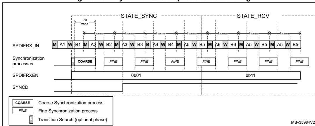
57.3.5 SPDIFRX synchronization
The synchronization phase starts when setting
SPDIFRXEN
to 01 or 11.
Figure 706
shows the synchronization process.
If the bit
WFA
of
SPDIFRX_CR
register is set to 1, then the peripheral must first detect activity on the selected
SPDIFRX_IN
line before starting the synchronization process. The activity detection is performed by detecting four transitions on the selected
SPDIFRX_IN
. The peripheral remains in this state until transitions are not detected. This function can be particularly helpful because the SPDIFRX switches in COARSE SYNC mode only if activity is present on the selected
SPDIFRX_IN
input, avoiding synchronization errors. See
Section 57.4: Programming procedures
for additional information.
The user can still set the SPDIFRX into STATE_IDLE by setting
SPDIFRXEN
to 0. If the
WFA
is set to 0, the peripheral starts the coarse synchronization without checking activity.
The next step consists on doing a first estimate of the thresholds (COARSE SYNC), in order to perform the fine synchronization (FINE SYNC). Due to disturbances of the SPDIFRX line, it can happen that the process is not executed first time right. For this purpose, the user can program the number of allowed re-tries (
NBTR
) before setting
SERR
error flag.
When the SPDIFRX is able to measure properly the duration of 24 and 40 consecutive symbols then the FINE SYNC is completed, the threshold values are updated, and the flag
SYNCD
is set to 1. Refer to
Section : Transition coder and preamble detector
for additional information.
Two kinds of errors are detected:
- • An overflow of the
TRCNT, which generally means that there is no valid S/PDIF stream in the input line. This overflow is indicated byTERRflag. - • The number of retries reached the programmed value. This means that strong jitter is present on the S/PDIF signal. This error is indicated by
SERRflag.
When the first FINE SYNC is completed, the reception of channel status (C) and user data (U) starts when the next “B” preamble is detected (see
Figure 710
). Then the user can read IEC-60958 C and U bits through
SPDIFRX_CSR
register. According to this information the user can then select the proper settings for
DRFMT
and
RXSTEO
. For example if the user detects that the current audio stream transports encoded data, then he can put
RXSTEO
to 0, and
DRFMT
to 10 prior to start data reception. Note that
DRFMT
and
RXSTEO
cannot be modified when
SPDIFRXEN
= 11. Writes to these fields are ignored if
SPDIFRXEN
is already 11, though these field can be changed with the same write instruction that causes
SPDIFRXEN
to become 11.
Then the SPDIFRX waits for
SPDIFRXEN
= 11 and the “B” preamble before starting saving audio samples.
Figure 706. Synchronization flowchart
graph TD
    Start([Initial Sync Process]) --> Wait[Wait for 4 transitions if WFA = 1, else skip this step]
    Wait --> Parallel[Parallel flows]
    Parallel --> TRCNT{TRCNT overflows ?}
    TRCNT -- N --> Parallel
    TRCNT -- Y --> TERR[ERROR: Sync failure ! TERR = 1]
    Parallel --> Coarse[Search for Longest/Shortest pulses for 70 transitions]
    Coarse --> CoarseTh[Compute COARSE thresholds (THLO, THHI)]
    CoarseTh --> FineSearch[Search for preamble for 70 transitions]
    FineSearch --> Preamble{preamble found within 70 trans. ?}
    Preamble -- N --> AttemptInc[ATTEMPT ++]
    Preamble -- Y --> Decode[Decode properly the next 40 symbols
Measurement of 24 and 40 symbols duration (WIDTH24, WIDTH40)]
    Decode --> SymbOK{Symb. decoding (1) OK ?}
    SymbOK -- N --> AttemptInc
    SymbOK -- Y --> FineTh[Compute FINE thresholds (THLO, THHI)]
    FineTh --> SetSyncD[Set SYNCD to 1]
    SetSyncD --> Done([Synchronization done])
    AttemptInc --> AttemptEq{ATTEMPT == NBTR ?}
    AttemptEq -- N --> Parallel
    AttemptEq -- Y --> SERR[ERROR: Sync failure ! SERR = 1]
    TERR --> SyncStopped([Sync stopped])
    SERR --> SyncStopped
(1) - The decoding is considered OK, when the symbols are properly decoded, and preamble occurs at the expected position
MSV35932V1
Refer to Frame structure and synchronization error for additional information concerning TRCNT overflow.
The FINE SYNC process is re-triggered every frame in order to update thresholds as shown in Figure 707 in order to continuously track S/PDIF synchronization.
Figure 707. Synchronization process scheduling
57.3.6 SPDIFRX handling
The software can control the state of the SPDIFRX through SPDIFRXEN field. The SPDIFRX can be into one of the following states:
- •
STATE_IDLE:
The peripheral is disabled, the spdifrx_ker_ck domain is reset. The spdifrx_pclk domain is functional. - •
STATE_SYNC:
The peripheral is synchronized to the stream, thresholds are updated regularly, user and channel status can be read via interrupt or DMA. The audio samples are not provided to receive buffer. - •
STATE_RCV:
The peripheral is synchronized to the stream, thresholds are updated regularly, user, channel status and audio samples can be read via interrupt or DMA channels. When SPDIFRXEN goes to 11, the SPDIFRX waits for “B” preamble before starting saving audio samples. - •
STOP_STATE:
The peripheral is no longer synchronized, the reception of the user, channel status and audio samples are stopped. It is expected that the software re-starts the SPDIFRX.
Figure 708 shows the possible states of the SPDIFRX, and how to transition from one state to the other. The bits under software control are followed by the mention “(SW)”, the bits under SPDIFRX control are followed by the mention “(HW)”.
Figure 708. SPDIFRX States
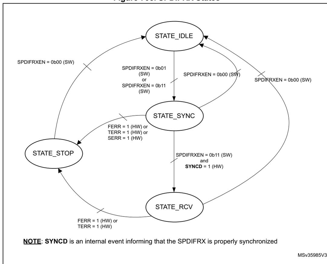
stateDiagram-v2
    [*] --> STATE_IDLE
    STATE_IDLE --> STATE_SYNC: SPDIFRXEN = 0b01 (SW) or SPDIFRXEN = 0b11 (SW)
    STATE_SYNC --> STATE_IDLE: SPDIFRXEN = 0b00 (SW)
    STATE_SYNC --> STATE_RCV: SPDIFRXEN = 0b11 (SW) and SYNCD = 1 (HW)
    STATE_RCV --> STATE_IDLE: SPDIFRXEN = 0b00 (SW)
    STATE_RCV --> STATE_STOP: FERR = 1 (HW) or TERR = 1 (HW)
    STATE_STOP --> STATE_IDLE: SPDIFRXEN = 0b00 (SW)
    STATE_STOP --> STATE_SYNC: FERR = 1 (HW) or TERR = 1 (HW) or SERR = 1 (HW)
NOTE: SYNCD is an internal event informing that the SPDIFRX is properly synchronized
MSv35985V3.
When SPDIFRX is in STATE_IDLE:
- • The software can transition to STATE_SYNC by setting SPDIFRXEN to 01 or 11
When SPDIFRX is in STATE_SYNC:
- • If the synchronization fails or if the received data are not properly decoded with no chance of recovery without a re-synchronization (FERR or SERR or TERR = 1), the SPDIFRX goes to STATE_STOP, and waits for software acknowledge.
- • When the synchronization phase is completed, if SPDIFRXEN = 01 the peripheral remains in this state.
- • At any time the software can set SPDIFRXEN to 0, then SPDIFRX returns immediately to STATE_IDLE. If a DMA transfer is on-going, it will properly be completed.
- • The SPDIFRX goes to STATE_RCV if SPDIFRXEN = 11 and if the SYNCD = 1
When SPDIFRX is in STATE_RCV:
- • If the received data are not properly decoded with no chance of recovery without a re-synchronization (FERR or SERR or TERR = 1), the SPDIFRX goes to STATE_STOP, and waits for software acknowledge.
- • At any time the software can set SPDIFRXEN to 0, then SPDIFRX returns immediately to STATE_IDLE. If a DMA transfer is on-going, it will properly be completed.
When SPDIFRX is in STATE_STOP:
- • The SPDIFRX stops reception and synchronization, and waits for the software to set the bit SPDIFRXEN to 0, in order to clear the error flags.
When SPDIFRXEN is set to 0, the SPDIFRX is disabled, meaning that all the state machines are reset, and RX_BUF is flushed. Note as well that flags FERR, SERR and TERR are reset.
57.3.7 Data reception management
The SPDIFRX offers a double buffer for the audio sample reception. A 32-bit buffer located into the spdifrx_ker_ck clock domain (RX_BUF), and the SPDIFRX_FMTx_DR register. The valid data contained into the RX_BUF are immediately transferred into SPDIFRX_FMTx_DR if SPDIFRX_FMTx_DR is empty.
The valid data contained into the RX_BUF are transferred into SPDIFRX_FMTx_DR when the two following conditions are reached:
- • The transition between the parity bit (P) and the next preamble is detected (this indicated that the word is completely received).
- • The SPDIFRX_FMTx_DR is empty.
Having a 2-word buffer gives more flexibility for the latency constraint.
The maximum latency allowed is \( T_{\text{SAMPLE}} - 2T_{\text{PCLK}} - 2T_{\text{spdifrx\_ker\_ck}} \)
Where \( T_{\text{SAMPLE}} \) is the audio sampling rate of the received stereo audio samples, \( T_{\text{PCLK}} \) is the period of spdifrx_pclk clock, and \( T_{\text{spdifrx\_ker\_ck}} \) is the period of spdifrx_ker_ck clock.
The SPDIFRX offers the possibility to use either DMA (spdifrx_dat_dma and spdifrx_ctrl_dma) or interrupts for transferring the audio samples into the memory. The recommended option is DMA, refer to Section 57.3.12: DMA interface for additional information.
The SPDIFRX offers several way on handling the received data. The user can either have a separate flow for control information and audio samples, or get them all together.
For each sub-frame, the data reception register SPDIFRX_FMTx_DR contains the 24 data bits, and optionally the V, U, C, PE status bits, and the PT (see Mixing data and control flow ).
Note that PE bit stands for parity error bit, and is set to 1 when a parity error is detected in the decoded sub-frame.
The PT field carries the preamble type (B, M or W).
V, U and C are a direct copy of the value received from the S/PDIF interface.
The bit DRFMT allows the selection between 3 audio formats as shown in Figure 709 .
This document describes 3 data registers: SPDIFRX_FMTx[2:0] (x = 2 to 0), but in reality there is only one physical data register, having 3 possible formats:
- • When DRFMT = 0, the format of the data register is the one described by SPDIFRX_FMT0_DR
- • When DRFMT = 1, the format of the data register is the one described by SPDIFRX_FMT1_DR
- • When DRFMT = 2, the format of the data register is the one described by SPDIFRX_FMT2_DR"
Figure 709. SPDIFRX_FMTx_DR register format
IEC60958 block format
IEC60958 sub-frame
| 0 - 3 | 4 | 5 | 6 | 7 | ... | 12 | ... | 25 | 26 | 27 | 28 | 29 | 30 | 31 | |||
| Sync Preamble | S0 | S1 | S2 | S3 | ... | S8 | ... | S21 | S22 | S23 | V | U | C | P | |||
SPDIFRX_FMT0_DR (i.e. DRFMT = 0b00)
| 31 | 30 | 29 | 28 | 27 | 26 | 25 | 24 | 23 | ... | 0 | |||||||||||||||||||||
| 0 | 0 | PT[1:0] or 0 | C or 0 | U or 0 | V or 0 | PE or 0 | S23 (MSb) | DR[23:0] | S0 (LSb) | ||||||||||||||||||||||
SPDIFRX_FMT1_DR (i.e. DRFMT = 0b01)
| 31 | ... | 8 | 7 | 6 | 5 | 4 | 3 | 2 | 1 | 0 | |||||||||||||||||||||
| S23 (MSb) | DR[23:0] | S0 (LSb) | 0 | 0 | PT[1:0] or 0 | C or 0 | U or 0 | V or 0 | PE or 0 | ||||||||||||||||||||||
SPDIFRX_FMT2_DR (i.e. DRFMT = 0b10)
| 31 | 30 - 17 | 16 | 15 | 14 - 1 | 0 | ||||||||||||||||||||||||||
| S23 (MSb) | DRNL2[15:0] | S8 (LSb) | S23 (MSb) | DRNL1[15:0] | S8 (LSb) | ||||||||||||||||||||||||||
| Ch A | Ch B | ||||||||||||||||||||||||||||||
Setting DRFMT to 00 or 01, offers the possibility to have the data either right or left aligned into the SPDIFRX_FMTx_DR register. The status information can be enabled or forced to zero according to the way the software wants to handle them.
The format given by DRFMT= 10 is interesting in non-linear mode, as only 16 bits per sub-frame are used. By using this format, the data of two consecutive sub-frames are stored into SPDIFRX_FMTx_DR, dividing by two the amount of memory footprint. Note that when RXSTEO = 1, there is no misalignment risks (i.e. data from ChA are always stored into SPDIFRX_FMTx_DR[31:16]). If RXSTEO = 0, then there is a misalignment risk in case of overrun situation. In that case SPDIFRX_FMTx_DR[31:16] always contain the oldest value and SPDIFRX_FMTx_DR[15:0] the more recent value (see Figure 711).
In this format the status information cannot be mixed with data, but the user can still get them through SPDIFRX_CSR register, and use a dedicated DMA channel or interrupt to transfer them to memory (see Section 57.3.8: Dedicated control flow )
Mixing data and control flow
The user can choose to use this mode in order to get the full flexibility of the handling of the control flow. The user can select which field must be kept into the data register (SPDIFRX_FMTx_DR).
- • When bit PMSK = 1, the parity error information is masked (set to 0), otherwise it is copied into SPDIFRX_FMTx_DR.
- • When bit VMSK = 1, the validity information is masked (set to 0), otherwise it is copied into SPDIFRX_FMTx_DR.
- • When bit CUMSK = 1, the channel status, and used data information are masked (set to 0), otherwise they are copied into SPDIFRX_FMTx_DR.
- • When bit PTMSK = 1, the preamble type is masked (set to 0), otherwise it is copied into SPDIFRX_FMTx_DR.
57.3.8 Dedicated control flow
The SPDIFRX offers the possibility to catch both user data and channel status information via a dedicated DMA channel. This feature allows the SPDIFRX to acquire continuously the channel status and user information. The acquisition starts at the beginning of a IEC 60958 block. Two fields are available to control this path: CBDMAEN and SPDIFRXEN. When SPDIFRXEN is set to 01 or 0x11, the acquisition is started, after completion of the synchronization phase. When 8 channel status and 16 user data bits are received, they are packed and stored into SPDIFRX_CSR register. A DMA request is triggered if the bit CBDMAEN is set to 1 (see Figure 710).
If CS[0] corresponds to the first bit of a new block, the bit SOB is set to 1. Refer to Section 57.5.8: Channel status register (SPDIFRX_CSR) . A bit is available (CHSEL) in order to select if the user wants to select channel status information (C) from the channel A or B.
Figure 710. Channel/user data format
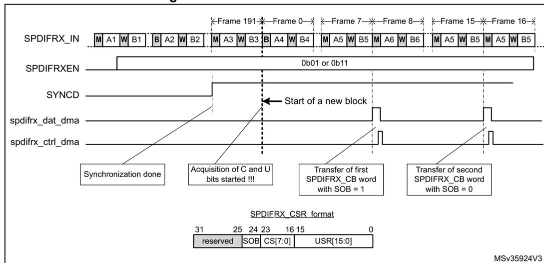
SPDIFRX_CSR format
| 31 | 25 | 24 | 23 | 16 | 15 | 0 |
| reserved | SOB | CS[7:0] | USR[15:0] | |||
MSv35924V3
Note: Once the first start of block is detected (B preamble), the SPDIFRX is checking the preamble type every 8 frames.
Note: Overrun error on SPDIFRX_FMTx_DR register does not affect this path.
57.3.9 Reception errors
Frame structure and synchronization error
The SPDIFRX, detects errors, when one of the following condition occurs:
- • The FERR bit is set to 1 on the following conditions:
- – For each of the 28 information bits, if one symbol transition sequence is not correct: for example if short pulses are not grouped by pairs.
- – If preambles occur to an unexpected place, or an expected preamble is not received.
- • The SERR bit is set when the synchronization fails, because the number of re-tries exceeded the programmed value.
- • The TERR bit is set when the counter used to estimate the width between two transitions overflows (TRCNT).
The overflow occurs when no transition is detected during 8192 periods of spdifrx_ker_ck clock. It represents at most a time interval of 11.6 frames.
When one of those flags goes to 1, the traffic on selected SPDIFRX_IN is then ignored, an interrupt is generated if the IFEIE bit of the SPDIFRX_CR register is set.
The normal procedure when one of those errors occur is:
- • Set SPDIFRXEN to 0 in order to clear the error flags
- • Set SPDIFRXEN to 01 or 11 in order to restart the SPDIFRX
Refer to Figure 708 for additional information.
Parity error
For each sub-frame, an even number of zeros and ones is expected inside the 28 information bits. If not, the parity error bit PERR is set in the SPDIFRX_SR register and an interrupt is generated if the parity interrupt enable PERRIE bit is set in the SPDIFRX_CR register. The reception of the incoming data is not paused, and the SPDIFRX continue to deliver data to SPDIFRX_FMTx_DR even if the interrupt is still pending.
The interrupt is acknowledged by clearing the PERR flag through PERRCF bit.
If the software wants to guarantee the coherency between the data read in the SPDIFRX_FMTx_DR register and the value of the bit PERR, the bit PMSK must be set to 0.
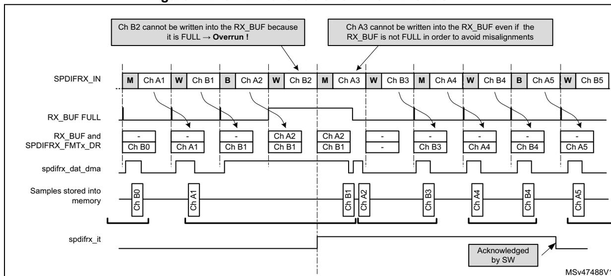
Overrun error
If both SPDIFRX_FMTx_DR and RX_BUF are full, while the SPDIFRX_DC needs to write a new sample in RX_BUF, this new sample is dropped, and an overrun condition is triggered. The overrun error flag OVR is set in the SPDIFRX_SR register and an interrupt is generated if the OVRIE bit of the SPDIFRX_CR register is set.
If the RXSTEO bit is set to 0, then as soon as the RX_BUF is empty, the SPDIFRX stores the next incoming data, even if the OVR flag is still pending. The main purpose is to reduce as much as possible the amount of lost samples. Note that the behavior is similar independently of DRFMT value. See Figure 711 .
Figure 711. S/PDIF overrun error when RXSTEO = 0
![Timing diagram for SPDIFRX overrun error when RXSTEO = 0 and DRFMT = 0b0x. It shows the SPDIFRX_IN signal with markers (M), words (W), and blocks (B) for channels A1, B1, A2, B2, A3, B3, A4, B4, A5, B5. The RX_BUF FULL signal goes high when the buffer is full. The RX_BUF and SPDIFRX_FMTx_DR content shows data being written into the buffer. The SPDIFRX_DMA_REQ signal is active. The Samples stored into memory show data being read from the buffer. The SPDIFRX_IRQ (OVR) signal is active and acknowledged by software. A callout indicates that Ch B2 cannot be written into the RX_BUF because it is FULL -> Overrun!, and another indicates that Ch A3 can be written into the RX_BUF. Timing diagram for SPDIFRX overrun error when RXSTEO = 0 and DRFMT = 0b10. It shows the IEC60958 block format with frames 191, 0, 1, 2, 3, and 4. Each frame contains markers (M), data (D), and words (W) for channels A and B. The RX_BUF FULL signal goes high when the buffer is full. The RXNE signal is active. The spdifrx_dat_dma signal is active. The spdifrx_it signal is active and acknowledged by software. The Data read from SPDIFRX_FMTx_DR shows data being read from the buffer. A callout indicates that RX_BUF cannot be emptied because SPDIF_RX is FULL, and another indicates that D6 is available and RX_BUF is FULL -> Overrun!. A final callout states that D6 is lost, SPDIFRX[31:16] contains the oldest data.](/RM0468-STM32H723-733-725-735-730/b6516cca52e913c7dffd80f63e4d2d7b_img.jpg)
DRFMT = 0b0x
DRFMT = 0b10
MSV35929V4
If the RXSTEO bit is set to 1, it means that stereo data are transported, then the SPDIFRX has to avoid misalignment between left and right channels. So the peripheral has to drop a second sample even if there is room inside the RX_BUF in order to avoid misalignment. Then the incoming samples can be written normally into the RX_BUF even if the OVR flag is still pending. Refer to Figure 712 .
The OVR flag is cleared by software, by setting the OVRFCF bit to 1.
Figure 712. S/PDIF overrun error when RXSTEO = 1
57.3.10 Clocking strategy
The SPDIFRX block needs two different clocks:
- • The APB clock (spdifrx_pclk), which is used for the register interface,
- • The spdifrx_ker_ck which is mainly used by the SPDIFRX_DC part. Those clocks are not supposed to be phase locked, so all signals crossing those clock domains are re-synchronized (SYNC block on Figure 698).
In order to decode properly the incoming S/PDIF stream the SPDIFRX_DC must re-sample the received data with a clock at least 11 times higher than the maximum symbol rate, or 704 times higher than the audio sample rate. For example if the user expects to receive a symbol rate to up to 12.288 MHz, the sample rate must be at least 135.2 MHz. The clock used by the SPDIFRX_DC is the spdifrx_ker_ck.
The frequency of the spdifrx_pclk must be at least equal to the symbol rate.
Table 458. Minimum spdifrx_ker_ck frequency versus audio sampling rate (1)
| Symbol rate | Minimum spdifrx_ker_ck frequency | Comments |
|---|---|---|
| 3.072 MHz | 33.8 MHz | For 48 kHz stream |
| 6.144 MHz | 67.6 MHz | For 96 kHz stream |
| 12.288 MHz | 135.2 MHz | For 192 kHz stream |
- 1. Check the RCC capabilities in order to verify which sampling rates can be supported.
57.3.11 Symbol clock generation
The SPDIFRX block provides a symbol clock on signal named spdifrx_symb_ck , which can be used as the reference kernel clock for another audio device such as SAI or SPI/I2S. It can be used for SPDIFRX to I2S bridge function.
The symbol clock is built using the values of WIDTH24, WIDTH40 and the symbol boundaries.
- • During the reception of the sub-frame sync preambles, the falling and rising edges of the symbol clock are built from the WIDTH24 and WIDTH40 values. Note that WIDTH24 and WIDTH40 are also used for the generation of the symbol clock, when the SPDIFRX is STATE_STOP or STATE_IDLE. See Table 459 for details.
- • During the reception of the sub-frame payload, the SPDIFRX uses the symbols boundaries to generate the rising edge, the WIDTH24 and WIDTH40 values for the generation of the falling edge.
The duty cycle of the symbol clock is close to 50% during the reception of the sub-frame payload. However, the duty cycle can be altered when the SPDIFRX transitions from a symbol clock generated with WIDTH24 and WIDTH40 to a clock generated by the symbol clock boundaries or vice-versa.
The symbol clock has an important jitter mainly due to:
- • The re-sampling of the S/PDIF signal with spdifrx_ker_ck clock
- • The transition of the symbol clock generation mode
For that reason the application must consider the quality degradation if the symbol clock is used as the reference clock for A/D or D/A converters.
The generation of this symbol clock is controlled by the CKSEN bit. When CKSEN = '1', the clock symbol is generated when the SPDIFRX completes successfully the first fine synchronization (SYNCD = 1), and when it receives correct data from the selected SPDIFRX input.
When the SPDIFRX goes to STATE_STOP, or STATE_IDLE, the symbol clock is gated if the bit CKSBKPEN = '0'. If the CKSBKPEN = '1', then a backup symbol clock is still generated if the SPDIFRX is properly synchronized (i.e. valid values available for WIDTH24 and WIDTH40). Table 459 gives more details on the conditions controlling the generation of the symbol clock.
Table 459. Conditions of spdifrx_symb_ck generation
| SPDIFRX states and conditions | CKSEN | CKSBKPEN | spdifrx_symb_ck state |
|---|---|---|---|
| Any state | 0 | X | Disabled |
Table 459. Conditions of spdifrx_symb_ck generation (continued)
| SPDIFRX states and conditions | CKSEN | CKSBKPEN | spdifrx_symb_ck state |
|---|---|---|---|
| – SPDIFRX in STATE_SYNC and completing successfully the fine synchronization (SYNCD = '1') or, – SPDIFRX in STATE_RCV, and valid data are received via the selected SPDIFRX input. | 0 | Enabled | |
| – SPDIFRX in STATE_IDLE or, – SPDIFRX in STATE_STOP or, – SPDIFRX did not complete the fine synchronization (on-going) – SPDIFRX is in STATE_RCV, but no data (transitions) detected on the selected SPDIFRX input. | 1 | 0 | Disabled |
| – SPDIFRX in STATE_IDLE, but with valid values for WIDTH40 and WIDTH24 or – SPDIFRX in STATE_SYNC and completing successfully the fine synchronization (SYNCD = '1') or, – SPDIFRX in STATE_SYNC the on-going fine synchronization is not completed, but WIDTH40 and WIDTH24 contain the valid values from the previous synchronization or, – SPDIFRX in STATE_RCV, and valid data are received via the selected SPDIFRX input or, – SPDIFRX in STATE_STOP, but with valid values for WIDTH40 and WIDTH24. | 1 | 1 | Enabled |
| – SPDIFRX in IDLE, with invalid values for WIDTH40 and WIDTH24 or, – SPDIFRX in STOP with invalid values for WIDTH40 and WIDTH24 (SERR = '1') or, – SPDIFRX in STATE_SYNC with invalid values for WIDTH40 and WIDTH24, and did not complete the on-going fine synchronization or, – SPDIFRX in STATE_RCV and no transitions detected on the selected SPDIFRX input | Disabled |
Note that when the flag SERR is set to '1', neither the symbol clock nor the backup clock can be generated, since there is no synchronization.
Note that when both CKSEN and CKSBKPEN are set to '1', the symbol clock looses some transitions when the SPDIFRX switches from STATE_SYNC or STATE_RCV to STATE_STOP, or STATE_IDLE.
The bits CKSEN and CKSBKPEN are located into Control register (SPDIFRX_CR) .
57.3.12 DMA interface
The SPDIFRX interface is able to perform communication using the DMA.
Note: The user must refer to product specifications for availability of the DMA controller.
The SPDIFRX offers two independent DMA channels:
- • A DMA channel dedicated to the data transfer
- • A DMA channel dedicated to the channel status and user data transfer
The DMA mode for the data can be enabled for reception by setting the RXDMAEN bit in the SPDIFRX_CR register. In this case, as soon as the SPDIFRX_FMTx_DR is not empty, the SPDIFRX interface sends a transfer request to the DMA. The DMA reads the data received through the SPDIFRX_FMTx_DR register without CPU intervention.
For the use of DMA for the control data refer to Section 57.3.8: Dedicated control flow .
57.3.13 Interrupt generation
An interrupt line is shared between:
- • Reception events for data flow (RXNE)
- • Reception event for control flow (CSRNE)
- • Data corruption detection (PERR)
- • Transfer flow interruption (OVR)
- • Frame structure and synchronization errors (SERR, TERR and FERR)
- • Start of new block interrupt (SBD)
- • Synchronization done (SYNCD)
Figure 713. SPDIFRX interface interrupt mapping diagram
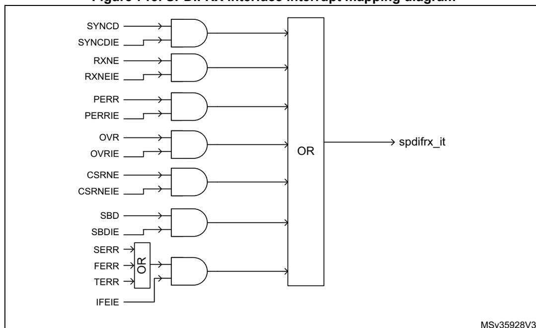
The diagram illustrates the interrupt mapping for the SPDIFRX interface. It features seven AND gates and one OR gate. The inputs to the AND gates are as follows:
- SYNCD and SYNCDIE (active-low) for the first AND gate.
- RXNE and RXNEIE (active-low) for the second AND gate.
- PERR and PERRIE (active-low) for the third AND gate.
- OVR and OVRIE (active-low) for the fourth AND gate.
- CSRNE and CSRNEIE (active-low) for the fifth AND gate.
- SBD and SBDIE (active-low) for the sixth AND gate.
- An OR gate combining SERR, FERR, and TERR (all active-low) for the seventh AND gate, along with IFEIE (active-low).
The outputs of all seven AND gates are connected to a single OR gate, which generates the final interrupt signal,
spdifrx_it
. The diagram is labeled with the identifier MSV35928V3.
Clearing interrupt source
- • RXNE is cleared when SPDIFRX_FMTx_DR register is read
- • CSRNE is cleared when SPDIFRX_CSR register is read
- • FERR is cleared when SPDIFRXEN is set to 0
- • SERR is cleared when SPDIFRXEN is set to 0
- • TERR is cleared when SPDIFRXEN is set to 0
- • Others are cleared through SPDIFRX_IFCR register
Note: The SBD event can only occur when the SPDIFRX is synchronized to the input stream (SYNCD = 1).
The SBD flag behavior is not guaranteed when the sub-frame which contains the B preamble is lost due to an overrun.
57.3.14 Register protection
The SPDIFRX block embeds some hardware protection avoid erroneous use of control registers. The table hereafter shows the bit field properties according to the SPDIFRX state.
Table 460. Bit field property versus SPDIFRX state
| Registers | Field | SPDIFRXEN | ||
|---|---|---|---|---|
| 00 (STATE_IDLE) | 01 (STATE_SYNC) | 11 (STATE_RCV) | ||
| SPDIFRX_CR | INSEL | rw | r | r |
| WFA | rw | r | r | |
| NBTR | rw | r | r | |
| CHSEL | rw | r | r | |
| CBDMAEN | rw | rw | rw | |
| PTMSK | rw | rw | rw | |
| CUMSK | rw | rw | rw | |
| VMSK | rw | rw | rw | |
| PMSK | rw | rw | rw | |
| DRFMT | rw | rw | r | |
| RXSTEO | rw | rw | r | |
| RXDMAEN | rw | rw | rw | |
| SPDIFRX_IMR | All fields | rw | rw | rw |
The table clearly shows that fields such as INSEL must be programmed when the SPDIFRX is in STATE_IDLE. In the others SPDIFRX states, the hardware prevents writing to this field.
Note: Even if the hardware allows the writing of CBDMAEN and RXDMAEN “on-the-fly”, it is not recommended to enable the DMA when the SPDIFRX already receives data.
Note: Each of the mask bits (such as PMSK, VMSK) can be changed “on-the-fly” at any SPDIFRX state, but any change does not affect data which are already hold in SPDIFRX_FMTx_DR.
57.4 Programming procedures
The following example illustrates a complete activation sequence of the SPDIFRX block. The data path and channel status and user information both use a dedicated DMA channel. The activation sequence is then split into the following steps:
- • Wait for valid data on the selected SPDIFRX_IN input
- • Synchronize to the S/PDIF stream
- • Read the channel status and user information in order to setup the complete audio path
- • Start data acquisition
A simple way to check if valid data are available into the SPDIFRX_IN line is to switch the SPDIFRX into the STATE_SYNC, with bit WFA set to 1. The description hereafter focuses on detection. It is also possible to implement this function as follows:
- • The software has to check from time to time (i.e. every 100 ms for example) if the SPDIFRX can find synchronization. This can be done by checking if the bit TERR is set. When it is set it indicates that no activity has been found.
- • Connect the SPDIFRX_IN input to an external interrupt event block in order to detect transitions of SPDIFRX_IN line. When activity is detected, then SPDIFRXEN can be set to 01 or 11.
For those two implementations, the bit WFA is set to 0.
57.4.1 Initialization phase
- • The initialization function looks like this:
- • Configure the DMA transfer for both audio samples and IEC60958 channel status and user information (DMA channel selection and activation, priority, number of data to transfer, circular/no circular mode, DMA interrupts)
- • Configure the destination address:
- – Configure the address of the SPDIFRX_CSR register as source address for IEC60958 channel status and user information
- – Configure the address of the SPDIFRX_FMTx_DR register as source address for audio samples
- – Enable the generation of the spdifrx_ker_ck. Refer to Table 458 in order to define the minimum clock frequency versus supported audio sampling rate. Note that the audio sampling rate of the received stream is not known in advance. This means that the user has to select a spdifrx_ker_ck frequency at least 704 times higher than the maximum audio sampling rate the application is supposed to handle: for example if the application is able to handle streams to up to 96 kHz, then \( F_{\text{spdifrx\_ker\_ck}} \) must be at least \( 704 \times 96 \text{ kHz} = 67.6 \text{ MHz} \)
- • Enable interrupt for errors and event signaling (IFEIE = SYNC DIE = OVRIE, PERRIE = 1, others set to 0). Note that SYNC DIE can be set to 0.
- • Configure the SPDIFRX_CR register:
- – INSEL must select the wanted input
- – NBTR = 2, WFA = 1 (16 re-tries allowed, wait for activity before going to synchronization phase),
- – PTMSK = CUMSK = 1 (Preamble, C and U bits are not mixed with data)
- – VMSK = PMSK = 0 (Parity error and validity bit mixed with data)
- – CHSEL = 0 (channels status are read from sub-frame A)
- – DRFMT = 01 (data aligned to the left)
- – RXSTEO = 1 (expected stereo mode linear)
- – CBDMAEN = RXDMAEN = 1 (enable DMA channels)
- – SPDIFRXEN = 01 (switch SPDIFRX to STATE_SYNC)
- • The CPU can enter in WFI mode
Then the CPU receives interrupts coming either from DMA or SPDIFRX.
57.4.2 Handling of interrupts coming from SPDIFRX
When an interrupt from the SPDIFRX is received, then the software has to check what is the source of the interrupt by reading the SPDIFRX_SR register.
- • If SYNCD is set to 1, then it means that the synchronization is properly completed. No action has to be performed in our case as the DMA is already programmed. The software just needs to wait for DMA interrupt in order to read channel status information.
The SYNCD flag must be cleared by setting SYNCD CF bit of SPDIFRX_IFCR register to 1.
- • If TERR or SERR or FERR are set to 1, the software has to set SPDIFRXEN to 0, and re-start from the initialization phase.
- – TERR indicates that a time-out occurs either during synchronization phase or after.
- – SERR indicates that the synchronization fails because the maximum allowed retries are reached.
- – FERR indicates that the reading of information after synchronization fails (such as unexpected preamble, bad data decoding).
- • If PERR is set to 1, it means that a parity error is detected, so one of the received audio sample or the channel status or user data bits are corrupted. The action taken here depends on the application: one action can be to drop the current channel status block as it is not reliable. There is no need to re-start from the initialization phase, as the synchronization is not lost.
The PERR flag must be cleared by setting PERR CF bit of SPDIFRX_IFCR register to 1.
57.4.3 Handling of interrupts coming from DMA
If an interrupt comes from the DMA channel used of the channel status (SPDIFRX_CSR):
If no error occurred (that is PERR), the CPU can start the decoding of channel information. For example bit 1 of the channel status informs the user if the current stream is linear or not. This information is very important in order to set-up the proper processing chain. In the same way, bits 24 to 27 of the channel status give the sampling frequency of the stream incoming stream.
Thanks to that information, the user can then configure the RXSTEO bit and DRFMT field prior to start the data reception. For example if the current stream is non linear PCM then RXSTEO is set to 0, and DRFMT is set to 10. Then the user can enable the data reception by setting SPDIFRXEN to 11.
The SOB bit, when set to 1 indicates the start of a new block. This information helps the software to identify the bit 0 of the channel status. Note that if the DMA generates an interrupt every time 24 values are transferred into the memory, then the first word always corresponds to the start of a new block.
If an interrupt comes from the DMA channel used of the audio samples (SPDIFRX_FMTx_DR):
The process performed here depends of the data type (linear or non-linear), and on the data format selected.
For example in linear mode, if PE or V bit is set a special processing can be performed locally in order to avoid spurs on output. In non-linear mode those bits are not important as data frame have their own checksum.
57.5 SPDIFRX interface registers
57.5.1 Control register (SPDIFRX_CR)
Only 32-bit accesses are allowed in this register.
Address offset: 0x00
Reset value: 0x0000 0000
| 31 | 30 | 29 | 28 | 27 | 26 | 25 | 24 | 23 | 22 | 21 | 20 | 19 | 18 | 17 | 16 |
|---|---|---|---|---|---|---|---|---|---|---|---|---|---|---|---|
| Res. | Res. | Res. | Res. | Res. | Res. | Res. | Res. | Res. | Res. | CKS BKP EN | CKSEN | Res. | INSEL[2:0] | ||
| rw | rw | rw | rw | rw | |||||||||||
| 15 | 14 | 13 | 12 | 11 | 10 | 9 | 8 | 7 | 6 | 5 | 4 | 3 | 2 | 1 | 0 |
| Res. | WFA | NBTR[1:0] | CHSEL | CBDMAEN | PTMSK | CUMSK | VMSK | PMSK | DRFMT[1:0] | RXSTE0 | RXDMAEN | SPDIFRXEN[1:0] | |||
| rw | rw | rw | rw | rw | rw | rw | rw | rw | rw | rw | rw | rw | rw | rw | |
Bits 31:22 Reserved, must be kept at reset value.
Bit 21 CKSBKPEN : Backup Symbol Clock Enable
This bit is set/reset by software
1: The SPDIFRX generates a backup symbol clock if CKSEN = '1'
0: The SPDIFRX does not generate a backup symbol clock
Bit 20 CKSEN : Symbol Clock Enable
This bit is set/reset by software
1: The SPDIFRX generates a symbol clock
0: The SPDIFRX does not generate a symbol clock
Bit 19 Reserved, must be kept at reset value.
Bits 18:16 INSEL[2:0] : SPDIFRX input selection (1)
000: SPDIFRX_IN1 selected
001: SPDIFRX_IN2 selected
010: SPDIFRX_IN3 selected
011: SPDIFRX_IN4 selected
other: reserved
Bit 15 Reserved, must be kept at reset value.
Bit 14 WFA : Wait for activity (1)
This bit is set/reset by software
1: The SPDIFRX waits for activity on SPDIFRX_IN line (4 transitions) before performing the synchronization
0: The SPDIFRX does not wait for activity on SPDIFRX_IN line before performing the synchronization
Bits 13:12 NBTR[1:0] : Maximum allowed re-tries during synchronization phase (1)
00: No re-try is allowed (only one attempt)
01: 3 re-tries allowed
10: 15 re-tries allowed
11: 63 re-tries allowed
Bit 11 CHSEL : Channel selection (1)
This bit is set/reset by software
1: The control flow takes the channel status from channel B
0: The control flow takes the channel status from channel A
Bit 10 CBDMAEN : Control buffer DMA enable for control flow (1)
This bit is set/reset by software
1: DMA mode is enabled for reception of channel status and used data information.
0: DMA mode is disabled for reception of channel status and used data information.
When this bit is set, the DMA request is made whenever the CSRNE flag is set.
Bit 9 PTMSK : Mask of preamble type bits (1)
This bit is set/reset by software
1: The preamble type bits are not copied into the SPDIFRX_FMTx_DR, zeros are written instead
0: The preamble type bits are copied into the SPDIFRX_FMTx_DR
Bit 8 CUMSK : Mask of channel status and user bits (1)
This bit is set/reset by software
1: The channel status and user bits are not copied into the SPDIFRX_FMTx_DR, zeros are written instead
0: The channel status and user bits are copied into the SPDIFRX_FMTx_DR
Bit 7 VMSK : Mask of validity bit (1)
This bit is set/reset by software
1: The validity bit is not copied into the SPDIFRX_FMTx_DR, a zero is written instead
0: The validity bit is copied into the SPDIFRX_FMTx_DR
Bit 6 PMSK : Mask parity error bit (1)
This bit is set/reset by software
1: The parity error bit is not copied into the SPDIFRX_FMTx_DR, a zero is written instead
0: The parity error bit is copied into the SPDIFRX_FMTx_DR
Bits 5:4 DRFMT[1:0] : RX data format (1)
This bit is set/reset by software
11: reserved
10: Data sample are packed by setting two 16-bit sample into a 32-bit word
01: Data samples are aligned in the left (MSB)
00: Data samples are aligned in the right (LSB)
Bit 3 RXSTEO : Stereo mode (1)
This bit is set/reset by software
1: The peripheral is in STEREO mode
0: The peripheral is in MONO mode
This bit is used in case of overrun situation in order to handle misalignment
Bit 2 RXDMAEN : Receiver DMA enable for data flow (1)
This bit is set/reset by software
1: DMA mode is enabled for reception.
0: DMA mode is disabled for reception.
When this bit is set, the DMA request is made whenever the RXNE flag is set.
Bits 1:0 SPDIFRXEN[1:0] : Peripheral block enable (1)
This field is modified by software.
It must be used to change the peripheral phase among the three possible states: STATE_IDLE, STATE_SYNC and STATE_RCV.
00: Disable SPDIFRX (STATE_IDLE).
01: Enable SPDIFRX synchronization only
10: Reserved
11: Enable SPDIF Receiver
Note: it is not possible to transition from STATE_RCV to STATE_SYNC, the user must first go the STATE_IDLE.
it is possible to transition from STATE_IDLE to STATE_RCV: in that case the peripheral transitions from STATE_IDLE to STATE_SYNC and as soon as the synchronization is performed goes to STATE_RCV.
1. Refer to Section 57.3.14: Register protection for additional information on fields properties.
57.5.2 Interrupt mask register (SPDIFRX_IMR)
Address offset: 0x04
Reset value: 0x0000 0000
| 31 | 30 | 29 | 28 | 27 | 26 | 25 | 24 | 23 | 22 | 21 | 20 | 19 | 18 | 17 | 16 |
|---|---|---|---|---|---|---|---|---|---|---|---|---|---|---|---|
| Res. | Res. | Res. | Res. | Res. | Res. | Res. | Res. | Res. | Res. | Res. | Res. | Res. | Res. | Res. | Res. |
| 15 | 14 | 13 | 12 | 11 | 10 | 9 | 8 | 7 | 6 | 5 | 4 | 3 | 2 | 1 | 0 |
| Res. | Res. | Res. | Res. | Res. | Res. | Res. | Res. | Res. | IFE IE | SYNCD IE | SBLK IE | OVR IE | PERR IE | CSRNE IE | RXNE IE |
| rw | rw | rw | rw | rw | rw | rw |
Bits 31:7 Reserved, must be kept at reset value.
Bit 6 IFEIE : Serial Interface Error Interrupt Enable
This bit is set and cleared by software.
0: Interrupt is inhibited
1: A SPDIFRX interface interrupt is generated whenever SERR=1, TERR=1 or FERR=1 in the SPDIFRX_SR register.
Bit 5 SYNCDIE : Synchronization Done
This bit is set and cleared by software.
0: Interrupt is inhibited
1: A SPDIFRX interface interrupt is generated whenever SYNCD = 1 in the SPDIFRX_SR register.
Bit 4 SBLKIE : Synchronization Block Detected Interrupt Enable
This bit is set and cleared by software.
0: Interrupt is inhibited
1: A SPDIFRX interface interrupt is generated whenever SBD = 1 in the SPDIFRX_SR register.
Bit 3 OVRIE : Overrun error Interrupt Enable
This bit is set and cleared by software.
0: Interrupt is inhibited
1: A SPDIFRX interface interrupt is generated whenever OVR=1 in the SPDIFRX_SR register
Bit 2 PERRIE : Parity error interrupt enable
This bit is set and cleared by software.
0: Interrupt is inhibited
1: A SPDIFRX interface interrupt is generated whenever PERR=1 in the SPDIFRX_SR register
Bit 1 CSRNEIE : Control Buffer Ready Interrupt Enable
This bit is set and cleared by software.
0: Interrupt is inhibited
1: A SPDIFRX interface interrupt is generated whenever CSRNE = 1 in the SPDIFRX_SR register.
Bit 0 RXNEIE : RXNE interrupt enable
This bit is set and cleared by software.
0: Interrupt is inhibited
1: A SPDIFRX interface interrupt is generated whenever RXNE=1 in the SPDIFRX_SR register
57.5.3 Status register (SPDIFRX_SR)
Address offset: 0x08
Reset value: 0x0000 0000
| 31 | 30 | 29 | 28 | 27 | 26 | 25 | 24 | 23 | 22 | 21 | 20 | 19 | 18 | 17 | 16 |
|---|---|---|---|---|---|---|---|---|---|---|---|---|---|---|---|
| Res. | WIDTH5[14:0] | ||||||||||||||
| r | r | r | r | r | r | r | r | r | r | r | r | r | r | r | |
| 15 | 14 | 13 | 12 | 11 | 10 | 9 | 8 | 7 | 6 | 5 | 4 | 3 | 2 | 1 | 0 |
| Res. | Res. | Res. | Res. | Res. | Res. | Res. | TERR | SERR | FERR | SYNCD | SBD | OVR | PERR | CSRNE | RXNE |
| r | r | r | r | r | r | r | r | r | |||||||
Bit 31 Reserved, must be kept at reset value.
Bits 30:16 WIDTH5[14:0] : duration of 5 symbols counted with spdifrx_ker_ck
This value represents the amount of spdifrx_ker_ck clock periods contained on a length of 5 consecutive symbols. This value can be used to estimate the S/PDIF symbol rate. Its accuracy is limited by the frequency of spdifrx_ker_ck.
For example if the spdifrx_ker_ck is fixed to 84 MHz, and WIDTH5 = 147d. The estimated sampling rate of the S/PDIF stream is:
\( F_s = 5 \times F_{\text{spdifrx\_ker\_ck}} / (\text{WIDTH5} \times 64) \sim 44.6 \text{ kHz} \) , so the closest standard sampling rate is 44.1 kHz.
Note that WIDTH5 is updated by the hardware when SYNCD goes high, and then every frame.
Bits 15:9 Reserved, must be kept at reset value.
Bit 8 TERR: time-out errorThis bit is set by hardware when the counter TRCNT reaches its max value. It indicates that the time interval between two transitions is too long. It generally indicates that there is no valid signal on SPDIFRX_IN input.
This flag is cleared by writing SPDIFRXEN to 0
An interrupt is generated if IFEIE=1 in the SPDIFRX_IMR register
0: No sequence error is detected
1: Sequence error is detected
Bit 7 SERR: synchronization errorThis bit is set by hardware when the synchronization fails due to amount of re-tries for NBTR.
This flag is cleared by writing SPDIFRXEN to 0
An interrupt is generated if IFEIE=1 in the SPDIFRX_IMR register.
0: No synchronization error is detected
1: Synchronization error is detected
Bit 6 FERR: framing errorThis bit is set by hardware when an error occurs during data reception: such as preamble not at the expected place, short transition not grouped by pairs.
This is set by the hardware only if the synchronization is completed (SYNCD = 1).
This flag is cleared by writing SPDIFRXEN to 0
An interrupt is generated if IFEIE=1 in the SPDIFRX_IMR register.
0: no Manchester Violation detected
1: Manchester Violation detected
Bit 5 SYNCD: synchronization doneThis bit is set by hardware when the initial synchronization phase is properly completed.
This flag is cleared by writing a 1 to its corresponding bit on SPDIFRX_IFCR register.
An interrupt is generated if SYNCDIE = 1 in the SPDIFRX_IMR register
0: Synchronization is pending
1: Synchronization is completed
Bit 4 SBD: synchronization block detectedThis bit is set by hardware when a “B” preamble is detected
This flag is cleared by writing a 1 to its corresponding bit on SPDIFRX_IFCR register.
An interrupt is generated if SBLKIE = 1 in the SPDIFRX_IMR register
0: No “B” preamble detected
1: “B” preamble is detected
Bit 3 OVR: overrun errorThis bit is set by hardware when a received data is ready to be transferred in the SPDIFRX_FMTx_DR register while RXNE = 1 and both SPDIFRX_FMTx_DR and RX_BUF are full.
This flag is cleared by writing a 1 to its corresponding bit on SPDIFRX_IFCR register.
An interrupt is generated if OVRIE=1 in the SPDIFRX_IMR register.
0: No Overrun error
1: Overrun error is detected
Note: When this bit is set, the SPDIFRX_FMTx_DR register content is not lost but the last data received are.
Bit 2 PERR : parity error
This bit is set by hardware when the data and status bits of the sub-frame received contain an odd number of 0 and 1.
This flag is cleared by writing a 1 to its corresponding bit on SPDIFRX_IFCR register.
An interrupt is generated if PIE = 1 in the SPDIFRX_IMR register.
0: No parity error
1: Parity error
Bit 1 CSRNE : the control buffer register is not empty
This bit is set by hardware when a valid control information is ready.
This flag is cleared when reading SPDIFRX_CSR register.
An interrupt is generated if CBRDYIE = 1 in the SPDIFRX_IMR register
0: No control word available on SPDIFRX_CSR register
1: A control word is available on SPDIFRX_CSR register
Bit 0 RXNE : read data register not empty
This bit is set by hardware when a valid data is available into SPDIFRX_FMTx_DR register.
This flag is cleared by reading the SPDIFRX_FMTx_DR register.
An interrupt is generated if RXNEIE=1 in the SPDIFRX_IMR register.
0: Data is not received
1: Received data is ready to be read.
57.5.4 Interrupt flag clear register (SPDIFRX_IFCR)
Address offset: 0x0C
Reset value: 0x0000 0000
| 31 | 30 | 29 | 28 | 27 | 26 | 25 | 24 | 23 | 22 | 21 | 20 | 19 | 18 | 17 | 16 |
|---|---|---|---|---|---|---|---|---|---|---|---|---|---|---|---|
| Res. | Res. | Res. | Res. | Res. | Res. | Res. | Res. | Res. | Res. | Res. | Res. | Res. | Res. | Res. | Res. |
| 15 | 14 | 13 | 12 | 11 | 10 | 9 | 8 | 7 | 6 | 5 | 4 | 3 | 2 | 1 | 0 |
| Res. | Res. | Res. | Res. | Res. | Res. | Res. | Res. | Res. | Res. | SYNCD CF | SBD CF | OVR CF | PERR CF | Res. | Res. |
| w | w | w | w |
Bits 31:6 Reserved, must be kept at reset value.
Bit 5 SYNCD CF : clears the synchronization done flag
Writing 1 in this bit clears the flag SYNCD in the SPDIFRX_SR register.
Reading this bit always returns the value 0.
Bit 4 SBD CF : clears the synchronization block detected flag
Writing 1 in this bit clears the flag SBD in the SPDIFRX_SR register.
Reading this bit always returns the value 0.
Bit 3 OVR CF : clears the overrun error flag
Writing 1 in this bit clears the flag OVR in the SPDIFRX_SR register.
Reading this bit always returns the value 0.
Bit 2 PERR CF : clears the parity error flag
Writing 1 in this bit clears the flag PERR in the SPDIFRX_SR register.
Reading this bit always returns the value 0.
Bits 1:0 Reserved, must be kept at reset value.
57.5.5 Data input register (SPDIFRX_FMT0_DR)
Address offset: 0x10
Reset value: 0x0000 0000
This register can take 3 different formats according to DRFMT. Here is the format when DRFMT = 00:
| 31 | 30 | 29 | 28 | 27 | 26 | 25 | 24 | 23 | 22 | 21 | 20 | 19 | 18 | 17 | 16 |
|---|---|---|---|---|---|---|---|---|---|---|---|---|---|---|---|
| Res. | Res. | PT[1:0] | C | U | V | PE | DR[23:16] | ||||||||
| r | r | r | r | r | r | r | r | r | r | r | r | r | r | r | r |
| 15 | 14 | 13 | 12 | 11 | 10 | 9 | 8 | 7 | 6 | 5 | 4 | 3 | 2 | 1 | 0 |
| DR[15:0] | |||||||||||||||
| r | r | r | r | r | r | r | r | r | r | r | r | r | r | r | r |
Bits 31:30 Reserved, must be kept at reset value.
Bits 29:28 PT[1:0] : preamble type
These bits indicate the preamble received.
00: not used
01: Preamble B received
10: Preamble M received
11: Preamble W received
Note that if PTMSK = 1, this field is forced to zero
Bit 27 C : channel status bit
Contains the received channel status bit, if CUMSK = 0, otherwise it is forced to 0
Bit 26 U : user bit
Contains the received user bit, if CUMSK = 0, otherwise it is forced to 0
Bit 25 V : validity bit
Contains the received validity bit if VMSK = 0, otherwise it is forced to 0
Bit 24 PE : parity error bit
Contains a copy of PERR bit if PMSK = 0, otherwise it is forced to 0
Bits 23:0 DR[23:0] : data value
Contains the 24 received data bits, aligned on D[23]
57.5.6 Data input register (SPDIFRX_FMT1_DR)
Address offset: 0x10
Reset value: 0x0000 0000
This register can take 3 different formats according to DRFMT. Here is the format when DRFMT = 01:
| 31 | 30 | 29 | 28 | 27 | 26 | 25 | 24 | 23 | 22 | 21 | 20 | 19 | 18 | 17 | 16 |
|---|---|---|---|---|---|---|---|---|---|---|---|---|---|---|---|
| DR[23:8] | |||||||||||||||
| r | r | r | r | r | r | r | r | r | r | r | r | r | r | r | r |
| 15 | 14 | 13 | 12 | 11 | 10 | 9 | 8 | 7 | 6 | 5 | 4 | 3 | 2 | 1 | 0 |
| DR[7:0] | Res. | Res. | PT[1:0] | C | U | V | PE | ||||||||
| r | r | r | r | r | r | r | r | r | r | r | r | r | r | ||
Bits 31:8 DR[23:0] : data value
Contains the 24 received data bits, aligned on D[23]
Bits 7:6 Reserved, must be kept at reset value.
Bits 5:4 PT[1:0] : preamble type
These bits indicate the preamble received.
00: not used
01: preamble B received
10: preamble M received
11: preamble W received
Note that if PTMSK = 1, this field is forced to zero
Bit 3 C : channel Status bit
Contains the received channel status bit, if CUMSK = 0, otherwise it is forced to 0
Bit 2 U : user bit
Contains the received user bit, if CUMSK = 0, otherwise it is forced to 0
Bit 1 V : validity bit
Contains the received validity bit if VMSK = 0, otherwise it is forced to 0
Bit 0 PE : parity error bit
Contains a copy of PERR bit if PMSK = 0, otherwise it is forced to 0
57.5.7 Data input register (SPDIFRX_FMT2_DR)
Address offset: 0x10
Reset value: 0x0000 0000
This register can take 3 different formats according to DRFMT.
The data format proposed when DRFMT = 10, is dedicated to non-linear mode, as only 16 bits are used (bits 23 to 8 from S/PDIF sub-frame).
| 31 | 30 | 29 | 28 | 27 | 26 | 25 | 24 | 23 | 22 | 21 | 20 | 19 | 18 | 17 | 16 |
| DRNL2[15:0] | |||||||||||||||
| r | r | r | r | r | r | r | r | r | r | r | r | r | r | r | r |
| 15 | 14 | 13 | 12 | 11 | 10 | 9 | 8 | 7 | 6 | 5 | 4 | 3 | 2 | 1 | 0 |
| DRNL1[15:0] | |||||||||||||||
| r | r | r | r | r | r | r | r | r | r | r | r | r | r | r | r |
Bits 31:16 DRNL2[15:0] : data value
This field contains the channel A
Bits 15:0 DRNL1[15:0] : data value
This field contains the channel B
57.5.8 Channel status register (SPDIFRX_CSR)
Address offset: 0x14
Reset value: 0x0000 0000
| 31 | 30 | 29 | 28 | 27 | 26 | 25 | 24 | 23 | 22 | 21 | 20 | 19 | 18 | 17 | 16 |
|---|---|---|---|---|---|---|---|---|---|---|---|---|---|---|---|
| Res. | Res. | Res. | Res. | Res. | Res. | Res. | SOB | CS[7:0] | |||||||
| r | r | r | r | r | r | r | r | r | |||||||
| 15 | 14 | 13 | 12 | 11 | 10 | 9 | 8 | 7 | 6 | 5 | 4 | 3 | 2 | 1 | 0 |
| USR[15:0] | |||||||||||||||
| r | r | r | r | r | r | r | r | r | r | r | r | r | r | r | r |
Bits 31:25 Reserved, must be kept at reset value.
Bit 24 SOB : start of block
This bit indicates if the bit CS[0] corresponds to the first bit of a new block
0: CS[0] is not the first bit of a new block
1: CS[0] is the first bit of a new block
Bits 23:16 CS[7:0] : channel A status information
Bit CS[0] is the oldest value
Bits 15:0 USR[15:0] : user data information
Bit USR[0] is the oldest value, and comes from channel A, USR[1] comes channel B.
So USR[n] bits come from channel A if n is even, otherwise they come from channel B.
57.5.9 Debug information register (SPDIFRX_DIR)
Address offset: 0x18
Reset value: 0x0000 0000
| 31 | 30 | 29 | 28 | 27 | 26 | 25 | 24 | 23 | 22 | 21 | 20 | 19 | 18 | 17 | 16 |
|---|---|---|---|---|---|---|---|---|---|---|---|---|---|---|---|
| Res. | Res. | Res. | TLO[12:0] | ||||||||||||
| r | r | r | r | r | r | r | r | r | r | r | r | r | |||
| 15 | 14 | 13 | 12 | 11 | 10 | 9 | 8 | 7 | 6 | 5 | 4 | 3 | 2 | 1 | 0 |
| Res. | Res. | Res. | TH[12:0] | ||||||||||||
| r | r | r | r | r | r | r | r | r | r | r | r | r | |||
Bits 31:29 Reserved, must be kept at reset value.
Bits 28:16 TLO[12:0] : threshold LOW ( \( TLO = 1.5 \times UI / T_{spdifrx\_ker\_ck} \) )
This field contains the current threshold LOW estimation. This value can be used to estimate the sampling rate of the received stream. The accuracy of TLO is limited to a period of the
\(
spdifrx\_ker\_ck
\)
. The sampling rate can be estimated as follow:
Sampling Rate =
\(
[2 \times TLO \times T_{spdifrx\_ker\_ck} \pm T_{spdifrx\_ker\_ck}] \times 2/3
\)
Note that TLO is updated by the hardware when SYNCD goes high, and then every frame.
Bits 15:13 Reserved, must be kept at reset value.
Bits 12:0 THI[12:0] : threshold HIGH ( \( THI = 2.5 \times UI / T_{spdifrx\_ker\_ck} \) )
This field contains the current threshold HIGH estimation. This value can be used to estimate the sampling rate of the received stream. The accuracy of THI is limited to a period of the
\(
spdifrx\_ker\_ck
\)
. The sampling rate can be estimated as follow:
Sampling Rate =
\(
[2 \times THI \times T_{spdifrx\_ker\_ck} \pm T_{spdifrx\_ker\_ck}] \times 2/5
\)
Note that THI is updated by the hardware when SYNCD goes high, and then every frame.
57.5.10 SPDIFRX interface register map
Table 461. SPDIFRX interface register map and reset values
| Offset | Register name | 31 | 30 | 29 | 28 | 27 | 26 | 25 | 24 | 23 | 22 | 21 | 20 | 19 | 18 | 17 | 16 | 15 | 14 | 13 | 12 | 11 | 10 | 9 | 8 | 7 | 6 | 5 | 4 | 3 | 2 | 1 | 0 |
|---|---|---|---|---|---|---|---|---|---|---|---|---|---|---|---|---|---|---|---|---|---|---|---|---|---|---|---|---|---|---|---|---|---|
| 0x00 | SPDIFRX_CR | Res. | Res. | Res. | Res. | Res. | Res. | Res. | Res. | Res. | Res. | CKSBKPEN | CKSEN | Res. | INSEL[2:0] | Res. | WFA | NBTR[1:0] | CHSEL | CBDMAEN | PTMSK | CUMSK | VMSK | PMSK | DRFMT[1:0] | RXSTEO | RXDMAEN | SPDIFRXEN[1:0] | |||||
| Reset value | 0 | 0 | 0 | 0 | 0 | 0 | 0 | 0 | 0 | 0 | 0 | 0 | 0 | 0 | 0 | 0 | 0 | 0 | 0 | 0 | |||||||||||||
| 0x04 | SPDIFRX_IMR | Res. | Res. | Res. | Res. | Res. | Res. | Res. | Res. | Res. | Res. | Res. | Res. | Res. | Res. | Res. | Res. | Res. | Res. | Res. | Res. | Res. | Res. | Res. | Res. | Res. | IFEIE | SYNCDIE | SBLKIE | OVRIE | PERRIE | CSRNEIE | RXNEIE |
| Reset value | 0 | 0 | 0 | 0 | 0 | 0 | 0 | ||||||||||||||||||||||||||
| 0x08 | SPDIFRX_SR | Res. | WIDTH5[14:0] | Res. | Res. | Res. | Res. | Res. | Res. | Res. | TERR | SERR | FERR | SYNCD | SBD | OVR | PERR | CSRNE | RXNE | ||||||||||||||
| Reset value | 0 | 0 | 0 | 0 | 0 | 0 | 0 | 0 | 0 | 0 | 0 | 0 | 0 | 0 | 0 | 0 | 0 | 0 | 0 | 0 | 0 | 0 | 0 | 0 | |||||||||
| 0x0C | SPDIFRX_IFCR | Res. | Res. | Res. | Res. | Res. | Res. | Res. | Res. | Res. | Res. | Res. | Res. | Res. | Res. | Res. | Res. | Res. | Res. | Res. | Res. | Res. | Res. | Res. | Res. | Res. | SYNCDCF | SBDCF | OVRCF | PERRCF | Res. | Res. | Res. |
| Reset value | 0 | 0 | 0 | 0 | |||||||||||||||||||||||||||||
| 0x10 | SPDIFRX_FMT0_DR | Res. | Res. | PT[1:0] | C | U | V | P | E | DR[23:0] | |||||||||||||||||||||||
| Reset value | 0 | 0 | 0 | 0 | 0 | 0 | 0 | 0 | 0 | 0 | 0 | 0 | 0 | 0 | 0 | 0 | 0 | 0 | 0 | 0 | 0 | 0 | 0 | 0 | 0 | 0 | 0 | 0 | 0 | 0 | |||
| 0x10 | SPDIFRX_FMT1_DR | DR[23:0] | Res. | PT[1:0] | C | U | V | P | E | ||||||||||||||||||||||||
| Reset value | 0 | 0 | 0 | 0 | 0 | 0 | 0 | 0 | 0 | 0 | 0 | 0 | 0 | 0 | 0 | 0 | 0 | 0 | 0 | 0 | 0 | 0 | 0 | 0 | 0 | 0 | 0 | 0 | 0 | 0 | 0 | ||
| 0x10 | SPDIFRX_FMT2_DR | DRNL2[15:0] | DRNL1[15:0] | ||||||||||||||||||||||||||||||
| Reset value | 0 | 0 | 0 | 0 | 0 | 0 | 0 | 0 | 0 | 0 | 0 | 0 | 0 | 0 | 0 | 0 | 0 | 0 | 0 | 0 | 0 | 0 | 0 | 0 | 0 | 0 | 0 | 0 | 0 | 0 | 0 | 0 | |
| 0x14 | SPDIFRX_CSR | Res. | Res. | Res. | Res. | Res. | Res. | SOB | CS[7:0] | USR[15:0] | |||||||||||||||||||||||
| Reset value | 0 | 0 | 0 | 0 | 0 | 0 | 0 | 0 | 0 | 0 | 0 | 0 | 0 | 0 | 0 | 0 | 0 | 0 | 0 | 0 | 0 | 0 | 0 | 0 | 0 | 0 | |||||||
Table 461. SPDIFRX interface register map and reset values (continued)
| Offset | Register name | 31 | 30 | 29 | 28 | 27 | 26 | 25 | 24 | 23 | 22 | 21 | 20 | 19 | 18 | 17 | 16 | 15 | 14 | 13 | 12 | 11 | 10 | 9 | 8 | 7 | 6 | 5 | 4 | 3 | 2 | 1 | 0 |
|---|---|---|---|---|---|---|---|---|---|---|---|---|---|---|---|---|---|---|---|---|---|---|---|---|---|---|---|---|---|---|---|---|---|
| 0x18 | SPDIFRX_DIR | Res | Res | Res | TLO[12:0] | Res | Res | Res | THI[12:0] | ||||||||||||||||||||||||
| Reset value | 0 | 0 | 0 | 0 | 0 | 0 | 0 | 0 | 0 | 0 | 0 | 0 | 0 | 0 | 0 | 0 | 0 | 0 | 0 | 0 | 0 | 0 | 0 | 0 | 0 | 0 | |||||||
Refer to Section 2.3 on page 131 for the register boundary addresses.