42. On-The-Fly decryption engine - AXI (OTFDEC)
42.1 Introduction
On-the-fly decryption engine OTFDEC allows to decrypt on-the-fly AXI traffic based on the read request address information. Four independent and non-overlapping encrypted regions can be defined in OTFDEC, with optional execute-only or execute-never enforcement per region.
OTFDEC is using AES-128 in counter mode to achieve the lowest possible latency. As a consequence, each time the content of one encrypted region is changed the entire region must be re-encrypted with a different cryptographic context (key or initialization vector). This constraint makes OTFDEC suitable to decrypt read-only data or code, stored for example in external NOR Flash memory.
Note: When OTFDEC is used in conjunction with OCTOSPI it is mandatory to access the external read-only memory using the memory map mode of the Flash memory controller.
CPU memories and OTFDEC follow little endian notation whereas AES hardware accelerator follows big endian notation. See AN5281 “How to use OTFDEC for encryption/decryption in trusted environment on STM32 MCUs” for more details.
42.2 OTFDEC main features
- • On-the-fly 128-bit decryption during STM32 OCTOSPI memory-mapped read operations (single or multiple).
- – Use of AES in counter (CTR) mode, with keystream FIFO (depth=4)
- – Support for any read size
- – Physical address of the reads is used for the encryption/decryption
- • Up to four independent encrypted regions
- – Granularity of the region definition: 4096 bytes
- – Region configuration write locking mechanism
- – Two optional decryption modes: execute-only and execute-never.
- – Each region has its own 128-bit key, two bytes firmware version, and eight bytes application-defined nonce. At least one of those must be changed each time an encryption is performed by the application.
- • Encryption keys confidentiality and integrity protection
- – Write-only registers, with software locking mechanism
- – Availability of 8-bit CRC as public key information
- • Support for STM32 Octo-SPI pre-fetching mechanism.
- • In execute-only mode, possibility to select an enhanced encryption mode to add a proprietary layer of protection on top of AES stream cipher.
- • AMBA AHB slave peripheral, accessible through 32-bit word single accesses only (otherwise an AHB bus error is generated, and write accesses are ignored).
- • Encryption mode
42.3 OTFDEC functional description
42.3.1 OTFDEC block diagram
Figure 368 shows the block diagram of the OTFDEC.
Figure 368. OTFDEC block diagram
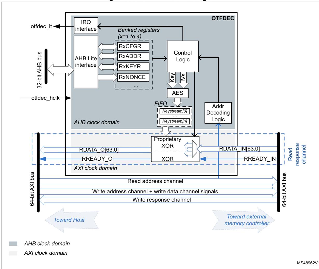
The diagram illustrates the internal architecture of the OTFDEC block. It is divided into two main clock domains: the AHB clock domain (shaded in light blue) and the AXI clock domain (shaded in light grey). In the AHB clock domain, an AHB Lite interface connects to a 32-bit AHB bus and an IRQ interface. The IRQ interface outputs the
otfdec_it
signal. The AHB Lite interface also connects to a set of Banked registers (labeled
RxCFGxR
,
RxADDRx
,
RxKEYRx
,
RxNONCE
for
\(
x=1
\)
to 4). These registers are connected to Control Logic, which in turn connects to an AES block. The AES block outputs a keystream to a FIFO, which contains
Keystream[0]
through
Keystream[n]
. The FIFO output is connected to a Proprietary XOR block. The Proprietary XOR block also receives data from the AXI clock domain and outputs
RDATA_O[63:0]
and
RREADY_O
signals. In the AXI clock domain, there is a 64-bit AXI bus interface. This interface includes a Read address channel, a Write address channel + write data channel signals, and a Write response channel. The Proprietary XOR block is connected to the Read address channel and outputs
RDATA_IN[63:0]
and
RREADY_IN
signals. The Read address channel is connected to a Read response channel. The diagram also shows the flow of data:
Toward Host
(indicated by a large blue arrow pointing left) and
Toward external memory controller
(indicated by a large blue arrow pointing right). A legend at the bottom left identifies the AHB clock domain and AXI clock domain. The reference code MS48962V1 is shown in the bottom right corner.
42.3.2 OTFDEC internal signals
Table 344 describes a list of useful to know internal signals available at OTFDEC level, not at the product level (on pads).
Table 344. OTFDEC internal input/output signals
| Signal name | Signal type | Description |
|---|---|---|
| otfdec_hclk | digital input | AHB bus clock |
| otfdec_it | digital output | OTFDEC global interrupt request |
42.3.3 OTFDEC on-the-fly decryption
Introduction
Typical usage for OTFDEC is shown on Figure 369.
Figure 369. Typical OTFDEC usage in the device
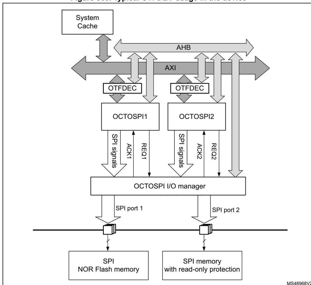
The diagram illustrates the typical OTFDEC usage in a device. At the top, a 'System Cache' is connected to an 'AHB' bus. The 'AHB' bus is connected to an 'AXI' bus. The 'AXI' bus is connected to two 'OTFDEC' blocks. Each 'OTFDEC' block is connected to an 'OCTOSPI1' and 'OCTOSPI2' block. These blocks are connected to an 'OCTOSPI I/O manager'. The 'OCTOSPI I/O manager' is connected to two 'SPI port' blocks, labeled 'SPI port 1' and 'SPI port 2'. 'SPI port 1' is connected to an 'SPI NOR Flash memory' block. 'SPI port 2' is connected to an 'SPI memory with read-only protection' block. Various signal lines are shown: 'SPI signals', 'ACK1', 'REQ1', 'ACK2', and 'REQ2' between the 'OCTOSPI' blocks and the 'OCTOSPI I/O manager'. A signal line labeled 'MS48968V2' is shown at the bottom right.
Original purpose of OTFDEC is to protect the confidentiality of execute-only firmware libraries, executed from external SPI NOR Flash memory devices. This scheme is part of
STM32 family of proprietary code read-out protection, leveraging on the capability to securely load secrets during microcontroller start up. OTFDEC protection also applies to read-only “code + data libraries”, and to execute-never, read-only data stored in external memory.
Note: OTFDEC provides optional execute-only and execute-never enforcement on any of the four encrypted regions.
A special locking scheme is available in OTFDEC in order to protect the integrity of the decryption keys and also to protect the other configurations against software denial of services attacks.
When OTFDEC is used in conjunction with OCTOSPI it is mandatory to access the external read-only memory using the memory map mode of the Flash memory controller.
OTFDEC architecture
OTFDEC principle is to analyze all read address channel transactions on the AXI interconnect between the host and a target, like the OCTOSPI controller shown on Figure 369 .
If the read request is within one of the four regions programmed in OTFDEC the control logic will trigger a keystream computation based on AES algorithm in counter mode. This keystream is then used to decrypt on-the-fly the data present in the read response channel, tying low the RREADY signal while the keystream information is being computed (this takes up to 11 cycles). Any accesses outside the enabled OTFDEC regions belong to a non-encrypted region.
Each OTFDEC regions are programmed through registers RxCFG, RxSTARTADDR, RxENDADDR, RxNONCER and RxKEYR, where x=1 to 4. In register RxCFG the MODE bits define whether the region is code (execute-only), data (execute-never), or both.
Granularity for the region determination is 4096 bytes.
Note: Although OTFDEC does not prevent region overlapping it is not a valid programming and it should be avoided by application software.
OTFDEC can decrypt incremental or wrap bursts only if they do not cross the 4096-byte aligned address boundaries.
42.3.4 AES in counter mode decryption
Figure 370 shows how OTFDEC uses industry standard Advanced Encryption Standard (AES) algorithm in counter chaining mode. This mode is specified by NIST in Special Publication 800-38A, Recommendation for Block Cipher Modes of Operation .
Figure 370. AES CTR decryption flow
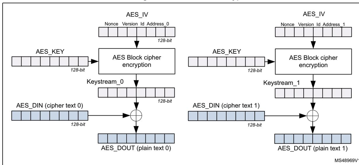
The diagram illustrates the AES CTR decryption flow for two parallel data blocks. Each block consists of the following components and steps:
- AES_IV: A 128-bit initialization vector with fields: Nonce, Version, Id, and Address (0 or 1).
- AES_KEY: A 128-bit key material.
- AES Block cipher encryption: A block that takes the AES_IV and AES_KEY as input and produces a 128-bit keystream (Keystream_0 or Keystream_1).
- AES_DIN (cipher text): A 128-bit input data block.
- XOR: A block that XORs the 128-bit keystream with the 128-bit AES_DIN to produce the 128-bit AES_DOUT (plain text).
The diagram is labeled MS48969V1.
Every 128-bit data block a special keystream information is computed using AES block cipher, as defined below:
- • The initialization vector \( AES\_IV[127:0] = RxNONCER[63:0] \parallel 0b0000\ 0000\ 0000\ 0000 \parallel RxCFGR[31:16] \parallel 0b00 \parallel (x-1) \parallel ReadAddress[31:4] \) (address modulo 128-bit)
- • The key material \( AES\_KEY[127:0] = RxKEYR3[31:0] \parallel RxKEYR2[31:0] \parallel RxKEYR1[31:0] \parallel RxKEYR0[31:0] \)
Note: Above \( x \) is the RegionID of the selected encrypted region ( \( x=1 \) to \( 4 \) ).
Resulting 128-bit keystream is XORed with 128-bit cipher text data to produce the 128-bit clear text data.
- •
\(
AES\_DIN
\)
and
\(
AES\_DOUT
\)
data blocks are constructed following the rule below:
\( AES\_Dx[127:0] = AXI\_word(@+0x8)[63:0] \parallel AXI\_word(@)[63:0] \) , where \( @ \) is the hexadecimal address used to compute the keystream.
When the read request is not within an encrypted region, or the decryption is not enabled in this region the 128-bit AXI data is not changed.
Note: When application sets the MODE bitfield to 11 in OTFDEC_RxCFGR an additional layer of protection is added on top of the AES stream cipher. This enhanced encryption mode is valid only in execute-only.
42.3.5 Flow control management
Figure 371 shows how OTFDEC manages two back-to-back AXI requests for a burst read of 4 words (256-bit). All 128-bit data blocks have contiguous address values.
Figure 371. OTFDEC flow control overview (dual burst read request)
![Figure 371. OTFDEC flow control overview (dual burst read request). The diagram illustrates the interaction between an AXI Master (CPU cache) and an AXI Slave (OctoSPI) for two back-to-back burst read requests. The master sends a read address with a burst size of 4 (256-bit). The slave responds with data blocks Data#1, Data#2, Data#3, and Data#4. The OTFDEC engine performs keystream computation for each data block, indicated by 'long' and 'short' latency labels. The keystreams are stored in KSTREAM FIFOs (KSTREAM[0] to KSTREAM[3]). The RREADY signal is shown low, indicating the engine is not ready to decrypt data. The RVALID signal is shown high, indicating valid data is available. The RLAST signal is shown high, indicating the end of the burst. The diagram also shows pre-fetching mechanisms (Pre-Fetch#1 to Pre-Fetch#4) and dependencies between data blocks and keystream computations. Numbered circles 1, 2, 3, and 4 highlight key areas: 1. RREADY signal, 2. RVALID signal, 3. Kstream FIFOs, 4. Pre-fetching mechanism.](/RM0468-STM32H723-733-725-735-730/37f995356a88c77d3eab8d1c30aab71e_img.jpg)
Few notes on this diagram:
- 1. OTFDEC enforces RREADY low as it is not ready to decrypt data (keystream computation).
- 2. OTFDEC does not enforce RREADY low as a valid mask is ready to XOR the incoming data. The decryption is done with zero latency, as expected.
- 3. The keystream FIFO is full. Next time a keystream is needed 11 clock cycles will be needed.
- 4. STM32 OctoSPI controller has a pre-fetching mechanism that greatly speed up any read request to an address that is consecutive to the last one. OTFDEC is able to manage this shorter latency thanks to the mask FIFO mechanism.
Figure 372 shows how OTFDEC manages an AXI request for a burst read of 4 words (256-bit), followed by a single read on an address that is not contiguous to the previous one.
Figure 372. OTFDEC flow control overview (burst then single read request)
![Figure 372. OTFDEC flow control overview (burst then single read request). The diagram shows the interaction between an AXI Master (Cpu cache) and an AXI Slave (OctoSPI). It details the flow of 'Control+address' and 'Read response channel (64-bit)' data. The OTFDEC engine performs 'Kstream computing' (Kstream, Kstream+1, Kstream+2, Kstream+3) and generates 'KSTREAM[0]' through 'KSTREAM[3]'. It shows data words (Data#1 to Data#4) and pre-fetch operations (Pre-Fetch#1 to Pre-Fetch#4). Timing signals RREADY, RVALID, and RLAST are shown at the bottom with numbered annotations 1 and 2 indicating where RREADY is held low.](/RM0468-STM32H723-733-725-735-730/45de88177dff176f5dbd7e0c8dc571d3_img.jpg)
Few notes on this diagram:
- 1. OTFDEC enforces RREADY low as it is not ready to decrypt data.
- 2. OTFDEC enforces RREADY low as pre-computed mask cannot be used for this request (the encrypted region address is not contiguous).
42.3.6 OTFDEC error management
OTFDEC automatically manages errors defined as below:
- • Illegal read to OTFDEC_RxKEYR registers
- • Illegal write to OTFDEC_RxKEYR registers while CONFIGLOCK or KEYLOCK="1" in OTFDEC_RxCFGR.
- • Illegal write to OTFDEC_RxCFGR, OTFDEC_RxSTARTADDR, OTFDEC_RxENDADDR or OTFDEC_RxNONCER registers while CONFIGLOCK="1" in OTFDEC_RxCFGR (x=1 to 4).
- • Illegal read to an execute-only region (MODE[1:0]=00 or 11), and illegal execution request to an execute-never region (MODE[1:0]=01). Such illegal requests return 0x0, without bus error.
- • Key error: read requests to an encrypted region after the key registers have been cleared by an abort event (tamper detection, unauthorized debug connection, untrusted boot, RDP level regression). Such read requests return 0x0, without bus error.
An interrupt can be generated by one or more of above errors if the bit SEIE, XONEIE or KEIE is set in OTFDEC_IER register, as explained in next Section 42.4 .
Note: After a key error OTFDEC keys must be initialized again, and a reset of OTFDEC might be needed if registers are locked.
42.4 OTFDEC interrupts
There are three independent maskable interrupt sources generated by the OTFDEC, signaling following security events:
- • Illegal read or write access to keys (SEIF flag), see Section 42.3.6
- • Illegal write to a region's configuration while CONFIGLOCK=1 (SEIF flag), see Section 42.3.6
- • Read access to an execute-only region (MODE[1:0]=00 or 11), execute access to an execute-never data region (MODE[1:0]=01). Both are triggering the XONEIF flag.
- • Key error (encrypted regions read as zero), triggering the KEIF flag. See Section 42.3.6 .
Interrupt sources are connected to the same global interrupt request signal.
You can enable or disable OTFDEC interrupt sources by setting corresponding SEIE, XONEIE or KEIE bits in OTFDEC_IER register, as described in Table 345 . Status of the interrupt event is found in OTFDEC_ISR register, and this event can be cleared using OTFDEC_ICR register.
Table 345. OTFDEC interrupt requests
| Interrupt event | Event flag | Enable control bit |
|---|---|---|
| Security Error | SEIF | SEIE |
| Execute-only, Execute-Never Error | XONEIF | XONEIE |
| Key Error | KEIF | KEIE |
42.5 OTFDEC application information
42.5.1 OTFDEC initialization process
Introduction
One key aspect of OTFDEC is the trusted initialization of its registers, as it involves secret keys and critical options like MODE bits.
Two trusted initialization schemes are recommended here below.
Note: Those sequence are for production code, as during firmware development it is not always recommended to lock the key or the region configuration.
Writes to configuration registers are effective when the configuration locks allow it, even if the region is enabled.
One key for all regions initialization scheme
In this scheme one entity owns the secret key used to decrypt the four protected regions. The recommended OTFDEC configuration sequence is described below:
- 3. For \( x=1 \) to 4 write the correct MODE[1:0] value in RxCFGGR register.
- 4. For \( x=1 \) to 4 program RxKEYR registers using the sequence described in KEYCRC (to have a valid CRC). Warning key registers are write only!
- 5. For \( x=1 \) to 4 check the key CRC. If OK set KEYLOCK bit in RxCFGR register. This bit cannot be cleared, i.e. the key registers in this region \( x \) are no more writable.
- 6. Do while you have a region
\(
x
\)
to decrypt. This task does not necessarily have to be performed by the entity that owns the decryption keys.
- a) Verify if the key CRC corresponds to the encrypted binary stored in the region.
- b) Fill the detailed information corresponding to this binary (nonce, start address, end address, version number).
- c) Enable decryption of this region using REG_EN.
- d) Set CONFIGLOCK bit in RxCFGR. This bit cannot be cleared, i.e. the region configuration is no more writable.
Caution: For a given region, when MODE bits are changed the key registers and associated CRC are cleared by hardware. As a consequence step 1 above must be done before step 2, and MODE bits must not be modified after step 2.
One key per region initialization scheme
In this scheme one entity can own the secret used to decrypt one (or more) protected region. The recommended OTFDEC configuration sequence is described below:
Do while you have a region x to decrypt. This task must be performed by the entity that owns the corresponding key.
- a) Write the correct MODE[1:0] value in RxCFGGR register.
- b) Program RxKEYR registers using the sequence described in KEYCRC (to have a valid key CRC). Warning key registers are write only!
- c) Check the key CRC. If OK set KEYLOCK bit in RxCFGGR register. This bit cannot be cleared, i.e. the key registers are no more writable.
- d) Fill the detailed information corresponding to the protected firmware (nonce, start address, end address, version number).
- e) Enable decryption of this region using REG_EN.
- f) Set CONFIGLOCK bit in RxCFGGR. This bit cannot be cleared, i.e. the region configuration is no more writable.
Caution: For a given region, when MODE bits are changed the key registers and associated CRC are cleared by hardware. As a consequence step a) above must be done before step b), and MODE bits must not be modified after step b).
42.5.2 OTFDEC and power management
Each time OTFDEC is reset the correct key loading sequence described in Section 42.5.1 must be performed (in this case KEYCRC equals to zero in OTFDEC_RxCFGGR registers).
It is recommended for application software to verify this point each time OTFDEC is reset by hardware.
42.5.3 Encrypting for OTFDEC
When MODE equals 00, 01 and 10
OTFDEC uses a standard AES in counter (CTR) mode to encrypt binary stored in a region with this MODE value. CTR chaining is defined in NIST Special Publication 800-38A, Recommendation for Block Cipher Modes of Operation .
When this mode is selected, any AES compatible hardware accelerator or library can be used to encrypt those protected libraries. Definition and endianness of the AES inputs and outputs are defined in Section 42.3.4: AES in counter mode decryption .
For more details, refer to AN5281 application note available on www.st.com .
When MODE equals to 11
OTFDEC uses a proprietary layer of protection on top of standard AES in counter mode when processing a code stored in a protected region with MODE[1:0] = 11.
Enhanced encryption mode can be used to increase the robustness against tampering.
When it is selected, two encryption scenarios are proposed:
- Use any device in RDP0 and a debugger to encrypt the code using a RSS service. Refer to AN5281 application note for more details.
- During a firmware install or update, use the OTFDEC in the device to encrypt the target code. For more details, refer to AN4992 application note (install) and UM2262 user manual (update) available on www.st.com .
42.5.4 OTFDEC Key CRC source code
Below is the CRC source code that can be used to compare with the result of the computation provided by OTFDEC in KEYCRC bitfield after loading the keys in OTFDEC_RxKEYR registers.
uint8_t getCRC(uint32_t * keyin)
{
    const uint8_t CRC7_POLY = 0x7;
    const uint32_t key_strobe[4] = {0xAA55AA55, 0x3, 0x18, 0xC0};
    uint8_t i, j, k, crc = 0x0;
    uint32_t keyval;

    for (j = 0; j < 4; j++)
    {
        keyval = *(keyin+j);
        if (j == 0)
        {
            keyval ^= key_strobe[0];
        }
        else
        {
            keyval ^= (key_strobe[j] << 24) | (crc << 16) | (key_strobe[j] << 8)
            | crc;
        }

        for (i = 0, crc = 0; i < 32; i++)
        {
            k = (((crc >> 7) ^ (keyval >> (31-i))&0xF)) & 1;
            crc <<= 1;
            if (k)
            {
                crc ^= CRC7_POLY;
            }
        }
        crc ^= 0x55;
    }
    return crc;
}
42.6 OTFDEC registers
42.6.1 OTFDEC region x configuration register (OTFDEC_RxCFGR)
Address offset: \( 0x20 + 0x30 \times (x - 1) \) ( \( x = 1 \) to 4)
Reset value: 0x0000 0000
Writes are ignored if CONFIGLOCK bit is set to 1.
| 31 | 30 | 29 | 28 | 27 | 26 | 25 | 24 | 23 | 22 | 21 | 20 | 19 | 18 | 17 | 16 |
|---|---|---|---|---|---|---|---|---|---|---|---|---|---|---|---|
| REGx_VERSION[15:0] | |||||||||||||||
| rw | rw | rw | rw | rw | rw | rw | rw | rw | rw | rw | rw | rw | rw | rw | rw |
| 15 | 14 | 13 | 12 | 11 | 10 | 9 | 8 | 7 | 6 | 5 | 4 | 3 | 2 | 1 | 0 |
| KEYCRC[7:0] | Res. | Res. | MODE[1:0] | Res. | KEYLO CK | CONFI GLOCK | REG_E N | ||||||||
| r | r | r | r | r | r | r | r | rw | rw | rs | rs | rw | |||
Bits 31:16 REGx_VERSION[15:0] : region firmware version
This 16-bit bitfield must be correctly initialized before the region corresponding REG_EN bit is set in the RxCFGR register.
Bits 15:8 KEYCRC[7:0] : region key 8-bit CRC
When KEYLOCK=0, KEYCRC bitfield is automatically computed by hardware while loading the key of this region in this exact sequence: KEYR0 then KEYR1 then KEYR2 then finally KEYR3 (all written once). A new computation starts as soon as a new valid sequence is initiated, and KEYCRC is read as zero until a valid sequence is completed.
When KEYLOCK=1, KEYCRC remains unchanged until the next reset.
CRC computation is an 8-bit checksum using the standard CRC-8-CCITT algorithm \( X^8 + X^2 + X + 1 \) (according the convention). Source code is available in this manual.
This field is read only.
Note: CRC information is updated only after the last bit of the key has been written.
Bits 7:6 Reserved, must be kept at reset value.
Bits 5:4 MODE[1:0] : operating mode
This bitfield selects the OTFDEC operating mode for this region:
- 00: Only instruction accesses are decrypted.
- 01: Only data accesses are decrypted.
- 10: All read accesses are decrypted (instruction or data).
- 11: Only instruction accesses are decrypted, and enhanced encryption mode is activated.
When MODE is not equal to 11 the standard AES encryption mode is activated.
When either of the MODE bits are changed the region's key and associated CRC are zeroed.
Bit 3 Reserved, must be kept at reset value.
Bit 2 KEYLOCK : region key lock
0: Writes to this region KEYRx registers are allowed.
1: Writes to this region KEYRx registers are ignored until next OTFDEC reset. KEYCRC bitfield is locked.
This bitfield is set once, i.e. if this bit is set it can only be reset to “0” if the OTFDEC is reset.
Bit 1 CONFIGLOCK : region config lock
0: Writes to this region CFGR1, STARTADDR, ENDADDR and NONCERx registers are allowed.
1: Writes to this region CFGR1, STARTADDR, ENDADDR and NONCERx registers are ignored until next OTFDEC reset.
This bit-field is set once, i.e. if this bit is set it can only be reset to “0” if OTFDEC is reset.
Setting this bit forces KEYLOCK bit to “1”.
Bit 0 REG_EN : region on-the-fly decryption enable
0: On-the-fly decryption is disabled for this region.
1: On-the-fly decryption is enabled for this region. Data are XORed with the corresponding keystream.
Note: When this bit is set region context (version, key, nonce) must be valid or garbage will be decrypted.
42.6.2 OTFDEC region x start address register (OTFDEC2_RxSTARTADDR)
Address offset: \( 0x24 + 0x30 * (x - 1) \) ( \( x = 1 \) to 4)
Reset value: 0x0000 0000
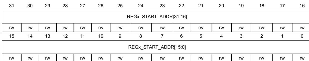
| 31 | 30 | 29 | 28 | 27 | 26 | 25 | 24 | 23 | 22 | 21 | 20 | 19 | 18 | 17 | 16 |
| REGx_START_ADDR[31:16] | |||||||||||||||
| rw | rw | rw | rw | rw | rw | rw | rw | rw | rw | rw | rw | rw | rw | rw | rw |
| 15 | 14 | 13 | 12 | 11 | 10 | 9 | 8 | 7 | 6 | 5 | 4 | 3 | 2 | 1 | 0 |
| REGx_START_ADDR[15:0] | |||||||||||||||
| rw | rw | rw | rw | rw | rw | rw | rw | rw | rw | rw | rw | rw | rw | rw | rw |
Bits 31:0 REGx_START_ADDR[31:0] : Region AXI start address
This register must be written before the region corresponding REG_EN bit in the RxCFGR register is set.
Writing this register while the region CONFIGLOCK bit in the RxCFGR register is set will be discarded.
Note: When determining the region the first 12 bits (LSB) and the last 4 bits (MSB) are ignored.
When this register is accessed in read the 4 MSB bits and the 12 LSB bits return zero.
42.6.3 OTFDEC region x end address register (OTFDEC_RxENDADDR)
Address offset: \( 0x28 + 0x30 * (x - 1) \) ( \( x = 1 \) to 4)
Reset value: 0x0000 0FFF
| 31 | 30 | 29 | 28 | 27 | 26 | 25 | 24 | 23 | 22 | 21 | 20 | 19 | 18 | 17 | 16 |
| REGx_END_ADDR[31:16] | |||||||||||||||
| rw | rw | rw | rw | rw | rw | rw | rw | rw | rw | rw | rw | rw | rw | rw | rw |
| 15 | 14 | 13 | 12 | 11 | 10 | 9 | 8 | 7 | 6 | 5 | 4 | 3 | 2 | 1 | 0 |
| REGx_END_ADDR[15:0] | |||||||||||||||
| rw | rw | rw | rw | rw | rw | rw | rw | rw | rw | rw | rw | rw | rw | rw | rw |
Bits 31:0 REGx_END_ADDR[31:0] : Region AXI end address
This register must be written before the region corresponding REG_EN bit in the RxCFGGR register is set, and RxENDADDR must be strictly greater than RxSTARTADDR to be valid.
Writing this register while the region CONFIGLOCK bit in the RxCFGGR register is set will be discarded.
Note: When determining the region the first 12 bits (LSB) and the last 4 bits (MSB) are ignored.
When this register is accessed in read the 4 MSB bits returns zeros and the 12 LSB bits return ones.
42.6.4 OTFDEC region x nonce register 0 (OTFDEC_RxNONCER0)
Address offset: 0x2C + 0x30 * (x - 1) (x = 1 to 4)
Reset value: 0x0000 0000
| 31 | 30 | 29 | 28 | 27 | 26 | 25 | 24 | 23 | 22 | 21 | 20 | 19 | 18 | 17 | 16 |
| REGx_NONCE[31:16] | |||||||||||||||
| rw | rw | rw | rw | rw | rw | rw | rw | rw | rw | rw | rw | rw | rw | rw | rw |
| 15 | 14 | 13 | 12 | 11 | 10 | 9 | 8 | 7 | 6 | 5 | 4 | 3 | 2 | 1 | 0 |
| REGx_NONCE[15:0] | |||||||||||||||
| rw | rw | rw | rw | rw | rw | rw | rw | rw | rw | rw | rw | rw | rw | rw | rw |
Bits 31:0 REGx_NONCE[31:0] : Region nonce, bits [31:0]
This register must be written before the region corresponding REG_EN bit in the RxCFGGR register is set.
Writing this register while the region CONFIGLOCK bit in the RxCFGGR register is set will be discarded.
42.6.5 OTFDEC region x nonce register 1 (OTFDEC_RxNONCER1)
Address offset: 0x30 + 0x30 * (x - 1) (x = 1 to 4)
Reset value: 0x0000 0000
| 31 | 30 | 29 | 28 | 27 | 26 | 25 | 24 | 23 | 22 | 21 | 20 | 19 | 18 | 17 | 16 |
| REGx_NONCE[63:48] | |||||||||||||||
| rw | rw | rw | rw | rw | rw | rw | rw | rw | rw | rw | rw | rw | rw | rw | rw |
| 15 | 14 | 13 | 12 | 11 | 10 | 9 | 8 | 7 | 6 | 5 | 4 | 3 | 2 | 1 | 0 |
| REGx_NONCE[47:32] | |||||||||||||||
| rw | rw | rw | rw | rw | rw | rw | rw | rw | rw | rw | rw | rw | rw | rw | rw |
Bits 31:0 REGx_NONCE[63:32] : Region nonce, bits [63:32]
Refer to the OTFDEC_RxNONCER0 register for description of the NONCE[63:0] bitfield.
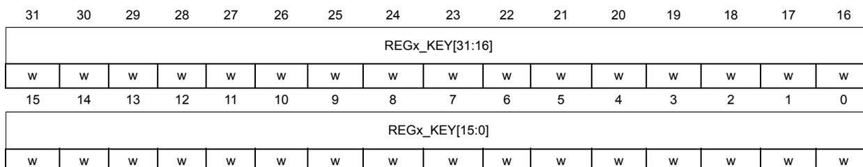
42.6.6 OTFDEC region x key register 0 (OTFDEC_RxKEYR0)
Address offset: \( 0x34 + 0x30 \times (x - 1) \) ( \( x = 1 \) to \( 4 \) )
Reset value: 0x0000 0000
| 31 | 30 | 29 | 28 | 27 | 26 | 25 | 24 | 23 | 22 | 21 | 20 | 19 | 18 | 17 | 16 |
| REGx_KEY[31:16] | |||||||||||||||
| w | w | w | w | w | w | w | w | w | w | w | w | w | w | w | w |
| 15 | 14 | 13 | 12 | 11 | 10 | 9 | 8 | 7 | 6 | 5 | 4 | 3 | 2 | 1 | 0 |
| REGx_KEY[15:0] | |||||||||||||||
| w | w | w | w | w | w | w | w | w | w | w | w | w | w | w | w |
Bits 31:0 REGx_KEY[31:0] : Region key, bits [31:0]
This register must be written before the region corresponding REG_EN bit in the RxCFGGR register is set.
Reading this register returns a zero value. Writing this register while the region CONFIGLOCK or KEYLOCK bit is set in the RxCFGGR register will be discarded.
Note: When application successfully changes MODE bits in RxCFGGR register RxKEYR registers and associated KEYCRC are erased.
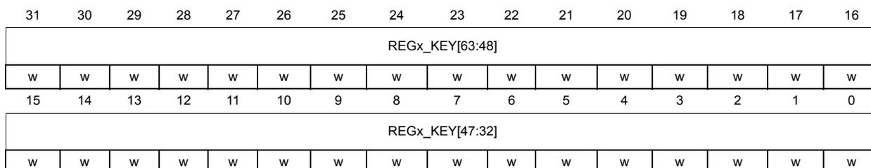
42.6.7 OTFDEC region x key register 1 (OTFDEC_RxKEYR1)
Address offset: \( 0x38 + 0x30 \times (x - 1) \) ( \( x = 1 \) to \( 4 \) )
Reset value: 0x0000 0000
| 31 | 30 | 29 | 28 | 27 | 26 | 25 | 24 | 23 | 22 | 21 | 20 | 19 | 18 | 17 | 16 |
| REGx_KEY[63:48] | |||||||||||||||
| w | w | w | w | w | w | w | w | w | w | w | w | w | w | w | w |
| 15 | 14 | 13 | 12 | 11 | 10 | 9 | 8 | 7 | 6 | 5 | 4 | 3 | 2 | 1 | 0 |
| REGx_KEY[47:32] | |||||||||||||||
| w | w | w | w | w | w | w | w | w | w | w | w | w | w | w | w |
Bits 31:0 REGx_KEY[63:32] : Region key, bits [63:32]
Refer to the OTFDEC_RxKEYR0 register for description of the KEY[127:0] bitfield.
42.6.8 OTFDEC region x key register 2 (OTFDEC_RxKEYR2)
Address offset: \( 0x3C + 0x30 \times (x - 1) \) ( \( x = 1 \) to \( 4 \) )
Reset value: 0x0000 0000

| 31 | 30 | 29 | 28 | 27 | 26 | 25 | 24 | 23 | 22 | 21 | 20 | 19 | 18 | 17 | 16 |
| REGx_KEY[95:80] | |||||||||||||||
| w | w | w | w | w | w | w | w | w | w | w | w | w | w | w | w |
| 15 | 14 | 13 | 12 | 11 | 10 | 9 | 8 | 7 | 6 | 5 | 4 | 3 | 2 | 1 | 0 |
|---|---|---|---|---|---|---|---|---|---|---|---|---|---|---|---|
| REGx_KEY[79:64] | |||||||||||||||
| w | w | w | w | w | w | w | w | w | w | w | w | w | w | w | w |
Bits 31:0
REGx_KEY[95:64]
: Region key, bits [95:64]
Refer to the OTFDEC_RxKEYR0 register for description of the KEY[127:0] bitfield.
42.6.9 OTFDEC region x key register 3 (OTFDEC_RxKEYR3)
Address offset: 0x40 + 0x30 * (x -1) (x = 1 to 4)
Reset value: 0x0000 0000
| 31 | 30 | 29 | 28 | 27 | 26 | 25 | 24 | 23 | 22 | 21 | 20 | 19 | 18 | 17 | 16 |
|---|---|---|---|---|---|---|---|---|---|---|---|---|---|---|---|
| REGx_KEY[127:112] | |||||||||||||||
| w | w | w | w | w | w | w | w | w | w | w | w | w | w | w | w |
| 15 | 14 | 13 | 12 | 11 | 10 | 9 | 8 | 7 | 6 | 5 | 4 | 3 | 2 | 1 | 0 |
| REGx_KEY[111:96] | |||||||||||||||
| w | w | w | w | w | w | w | w | w | w | w | w | w | w | w | w |
Bits 31:0
REGx_KEY[127:96]
: Region key, bits [127:96]
Refer to the OTFDEC_RxKEYR0 register for description of the KEY[127:0] bitfield.
42.6.10 OTFDEC interrupt status register (OTFDEC_ISR)
Address offset: 0x300
Reset value: 0x0000 0000
| 31 | 30 | 29 | 28 | 27 | 26 | 25 | 24 | 23 | 22 | 21 | 20 | 19 | 18 | 17 | 16 |
|---|---|---|---|---|---|---|---|---|---|---|---|---|---|---|---|
| Res. | Res. | Res. | Res. | Res. | Res. | Res. | Res. | Res. | Res. | Res. | Res. | Res. | Res. | Res. | Res. |
| 15 | 14 | 13 | 12 | 11 | 10 | 9 | 8 | 7 | 6 | 5 | 4 | 3 | 2 | 1 | 0 |
| Res. | Res. | Res. | Res. | Res. | Res. | Res. | Res. | Res. | Res. | Res. | Res. | Res. | KEIF | XONEIF | SEIF |
| r | r | r |
Bits 31:3 Reserved, must be kept at reset value.
Bit 2 KEIF: Key Error Interrupt Flag status
This bit is set by hardware and read only by application. Bit is set when a read access occurs on any encrypted region following the reset of the key registers by an abort event (tamper detection, unauthorized debugger connection, untrusted boot, RDP level regression).
Bit is cleared when application sets in OTFDEC_ICR the corresponding bit to “1”.
0: OTFDEC is operating properly.
1: Read access detected on an enabled encrypted region following an abort event. OTFDEC returns a zeroed value for the read, and an optional interrupt is generated if bit KEIE is set to “1” in OTFDEC_IER register.
After KEIF is set any subsequent read to any enabled encrypted region returns a zeroed value. This state remains until OTFDEC keys are initialized again.
Bit 1 XONEIF: Execute-only execute-Never Error Interrupt Flag status
This bit is set by hardware and read only by application. Bit is set when a read access and not an instruction fetch is detected on any encrypted region with MODE bits set to 00 or 11. It is also set when an instruction fetch and not a read access is detected on any encrypted region with MODE bits set to 01.
Bit is cleared when application sets in OTFDEC_ICR the corresponding bit to “1”.
0: No execute-only error status. No interrupt pending.
1: Read access detected on one region with MODE bits set to 00 or 11, or execute access detected on one region with MODE bits set to 01. OTFDEC returns a zeroed value for the illegal access, and an optional interrupt is generated if bit XONEIE is set to “1” in OTFDEC_IER register.
Bit 0 SEIF: Security Error Interrupt Flag status
This bit is set by hardware and read only by application. Bit is set when at least one security error has been detected (illegal access to keys, illegal write on locked configuration).
Bit is cleared when application sets in OTFDEC_ICR the corresponding bit to “1”.
0: No security error status. No interrupt pending.
1: Security error flag status, with interrupt pending. Actual interrupt generation is dependent on OTFDEC_IER corresponding bit SEIE.
42.6.11 OTFDEC interrupt clear register (OTFDEC_ICR)
Address offset: 0x304
Reset value: 0x0000 0000
| 31 | 30 | 29 | 28 | 27 | 26 | 25 | 24 | 23 | 22 | 21 | 20 | 19 | 18 | 17 | 16 |
|---|---|---|---|---|---|---|---|---|---|---|---|---|---|---|---|
| Res. | Res. | Res. | Res. | Res. | Res. | Res. | Res. | Res. | Res. | Res. | Res. | Res. | Res. | Res. | Res. |
| 15 | 14 | 13 | 12 | 11 | 10 | 9 | 8 | 7 | 6 | 5 | 4 | 3 | 2 | 1 | 0 |
| Res. | Res. | Res. | Res. | Res. | Res. | Res. | Res. | Res. | Res. | Res. | Res. | Res. | KEIF | XONEIF | SEIF |
| w | w | w | |||||||||||||
Bits 31:3 Reserved, must be kept at reset value.
Bit 2 KEIF : Key Error Interrupt Flag clear
This bit is written by application, and always reads as 0.
0: KEIF flag status is not affected
1: KEIF flag status is cleared in OTFDEC_ISR register
Note: Clearing KEIF does not solve the source of the problem (bad key registers). To be able to read or execute again any encrypted region, OTFDEC key registers must properly initialized, again.
Bit 1 XONEIF : Execute-only execute-Never Error Interrupt Flag clear
This bit is written by application, and always reads as 0.
0: XONEIF flag status is not affected
1: XONEIF flag status is cleared in OTFDEC_ISR register
Bit 0 SEIF : Security Error Interrupt Flag clear
This bit is written by application, and always reads as 0.
0: SEIF flag status is not affected
1: SEIF flag status is cleared in OTFDEC_ISR register
42.6.12 OTFDEC interrupt enable register (OTFDEC_IER)
Address offset: 0x308
Reset value: 0x0000 0000
| 31 | 30 | 29 | 28 | 27 | 26 | 25 | 24 | 23 | 22 | 21 | 20 | 19 | 18 | 17 | 16 |
|---|---|---|---|---|---|---|---|---|---|---|---|---|---|---|---|
| Res. | Res. | Res. | Res. | Res. | Res. | Res. | Res. | Res. | Res. | Res. | Res. | Res. | Res. | Res. | Res. |
| 15 | 14 | 13 | 12 | 11 | 10 | 9 | 8 | 7 | 6 | 5 | 4 | 3 | 2 | 1 | 0 |
| Res. | Res. | Res. | Res. | Res. | Res. | Res. | Res. | Res. | Res. | Res. | Res. | Res. | KEIE | XONEIE | SEIE |
| rw | rw | rw |
Bits 31:3 Reserved, must be kept at reset value.
Bit 2 KEIE : Key Error Interrupt Enable
This bit is read and written by application. It controls the OTFDEC interrupt generation when KEIF flag status is set.
0: Interrupt generation on key error flag KEIF is disabled (masked)
1: Interrupt generation on key error flag KEIF is enabled (not masked)
Bit 1 XONEIE : Execute-only execute-Never Error Interrupt Enable
This bit is read and written by application. It controls the OTFDEC interrupt generation when XONEIF flag status is set.
0: Interrupt generation on execute-only error XONEIF is disabled (masked)
1: Interrupt generation on execute-only error XONEIF is enabled (not masked)
Bit 0 SEIE : Security Error Interrupt Enable
This bit is read and written by application. It controls the OTFDEC interrupt generation when SEIF flag status is set.
0: Interrupt generation on security error SEIF is disabled (masked)
1: Interrupt generation on security error SEIF is enabled (not masked)
42.6.13 OTFDEC register map
Table 346 gives the summary OTFDEC register map and reset values.
Table 346. OTFDEC register map and reset values
| Offset | Register name reset value | 31 | 30 | 29 | 28 | 27 | 26 | 25 | 24 | 23 | 22 | 21 | 20 | 19 | 18 | 17 | 16 | 15 | 14 | 13 | 12 | 11 | 10 | 9 | 8 | 7 | 6 | 5 | 4 | 3 | 2 | 1 | 0 |
|---|---|---|---|---|---|---|---|---|---|---|---|---|---|---|---|---|---|---|---|---|---|---|---|---|---|---|---|---|---|---|---|---|---|
| 0x00 - 0x1C | Reserved | Res. | Res. | Res. | Res. | Res. | Res. | Res. | Res. | Res. | Res. | Res. | Res. | Res. | Res. | Res. | Res. | Res. | Res. | Res. | Res. | Res. | Res. | Res. | Res. | Res. | Res. | Res. | Res. | Res. | Res. | Res. | Res. |
| 0x20 | OTFDEC_R1CFGR | REG1_VERSION[15:0] | KEYCRC[7:0] | Res. | Res. | MODE[1:0] | Res. | KEYLOCK. | CONFIGLOCK. | REG_EN | |||||||||||||||||||||||
| Reset value | 0 | 0 | 0 | 0 | 0 | 0 | 0 | 0 | 0 | 0 | 0 | 0 | 0 | 0 | 0 | 0 | 0 | 0 | 0 | 0 | 0 | 0 | 0 | 0 | 0 | 0 | 0 | 0 | 0 | 0 | 0 | 0 | |
| 0x24 | OTFDEC_R1STARTADDR | REG1_START_ADD[31:0] | |||||||||||||||||||||||||||||||
| Reset value | 0 | 0 | 0 | 0 | 0 | 0 | 0 | 0 | 0 | 0 | 0 | 0 | 0 | 0 | 0 | 0 | 0 | 0 | 0 | 0 | 0 | 0 | 0 | 0 | 0 | 0 | 0 | 0 | 0 | 0 | 0 | 0 | |
| 0x28 | OTFDEC_R1ENDADDR | REG1_END_ADD[31:0] | |||||||||||||||||||||||||||||||
| Reset value | 0 | 0 | 0 | 0 | 0 | 0 | 0 | 0 | 0 | 0 | 0 | 0 | 0 | 0 | 0 | 0 | 0 | 0 | 0 | 0 | 1 | 1 | 1 | 1 | 1 | 1 | 1 | 1 | 1 | 1 | 1 | 1 | |
| 0x2C | OTFDEC_R1NONCER0 | REG1_NONCE[31:0] | |||||||||||||||||||||||||||||||
| Reset value | 0 | 0 | 0 | 0 | 0 | 0 | 0 | 0 | 0 | 0 | 0 | 0 | 0 | 0 | 0 | 0 | 0 | 0 | 0 | 0 | 0 | 0 | 0 | 0 | 0 | 0 | 0 | 0 | 0 | 0 | 0 | 0 | |
| 0x30 | OTFDEC_R1NONCER1 | REG1_NONCE[63:32] | |||||||||||||||||||||||||||||||
| Reset value | 0 | 0 | 0 | 0 | 0 | 0 | 0 | 0 | 0 | 0 | 0 | 0 | 0 | 0 | 0 | 0 | 0 | 0 | 0 | 0 | 0 | 0 | 0 | 0 | 0 | 0 | 0 | 0 | 0 | 0 | 0 | 0 | |
| 0x34 | OTFDEC_R1KEYR0 | REG1_KEY[31:0] | |||||||||||||||||||||||||||||||
| Reset value | 0 | 0 | 0 | 0 | 0 | 0 | 0 | 0 | 0 | 0 | 0 | 0 | 0 | 0 | 0 | 0 | 0 | 0 | 0 | 0 | 0 | 0 | 0 | 0 | 0 | 0 | 0 | 0 | 0 | 0 | 0 | 0 | |
| 0x38 | OTFDEC_R1KEYR1 | REG1_KEY[63:32] | |||||||||||||||||||||||||||||||
| Reset value | 0 | 0 | 0 | 0 | 0 | 0 | 0 | 0 | 0 | 0 | 0 | 0 | 0 | 0 | 0 | 0 | 0 | 0 | 0 | 0 | 0 | 0 | 0 | 0 | 0 | 0 | 0 | 0 | 0 | 0 | 0 | 0 | |
| 0x3C | OTFDEC_R1KEYR2 | REG1_KEY[95:64] | |||||||||||||||||||||||||||||||
| Reset value | 0 | 0 | 0 | 0 | 0 | 0 | 0 | 0 | 0 | 0 | 0 | 0 | 0 | 0 | 0 | 0 | 0 | 0 | 0 | 0 | 0 | 0 | 0 | 0 | 0 | 0 | 0 | 0 | 0 | 0 | 0 | 0 | |
| 0x40 | OTFDEC_REG1_KEYR3 | REG1_KEY[127:96] | |||||||||||||||||||||||||||||||
| Reset value | 0 | 0 | 0 | 0 | 0 | 0 | 0 | 0 | 0 | 0 | 0 | 0 | 0 | 0 | 0 | 0 | 0 | 0 | 0 | 0 | 0 | 0 | 0 | 0 | 0 | 0 | 0 | 0 | 0 | 0 | 0 | 0 | |
| 0x44 - 0x4C | Reserved | Res. | Res. | Res. | Res. | Res. | Res. | Res. | Res. | Res. | Res. | Res. | Res. | Res. | Res. | Res. | Res. | Res. | Res. | Res. | Res. | Res. | Res. | Res. | Res. | Res. | Res. | Res. | Res. | Res. | Res. | Res. | Res. |
| Reset value | |||||||||||||||||||||||||||||||||
| 0x50 | OTFDEC_R2CFGR | REG2_VERSION[15:0] | KEYCRC[7:0] | Res. | Res. | MODE[1:0] | Res. | KEYLOCK. | CONFIGLOCK. | REG_EN | |||||||||||||||||||||||
| Reset value | 0 | 0 | 0 | 0 | 0 | 0 | 0 | 0 | 0 | 0 | 0 | 0 | 0 | 0 | 0 | 0 | 0 | 0 | 0 | 0 | 0 | 0 | 0 | 0 | 0 | 0 | 0 | 0 | 0 | 0 | 0 | 0 | |
Table 346. OTFDEC register map and reset values (continued)
| Offset | Register name reset value | 31 | 30 | 29 | 28 | 27 | 26 | 25 | 24 | 23 | 22 | 21 | 20 | 19 | 18 | 17 | 16 | 15 | 14 | 13 | 12 | 11 | 10 | 9 | 8 | 7 | 6 | 5 | 4 | 3 | 2 | 1 | 0 |
|---|---|---|---|---|---|---|---|---|---|---|---|---|---|---|---|---|---|---|---|---|---|---|---|---|---|---|---|---|---|---|---|---|---|
| 0x054 | OTFDEC_R2STARTADDR | REG2_START_ADD[31:0] | |||||||||||||||||||||||||||||||
| Reset value | 0 | 0 | 0 | 0 | 0 | 0 | 0 | 0 | 0 | 0 | 0 | 0 | 0 | 0 | 0 | 0 | 0 | 0 | 0 | 0 | 0 | 0 | 0 | 0 | 0 | 0 | 0 | 0 | 0 | 0 | 0 | 0 | |
| 0x058 | OTFDEC_R2ENDADDR | REG2_END_ADD[31:0] | |||||||||||||||||||||||||||||||
| Reset value | 0 | 0 | 0 | 0 | 0 | 0 | 0 | 0 | 0 | 0 | 0 | 0 | 0 | 0 | 0 | 0 | 0 | 0 | 0 | 0 | 0 | 1 | 1 | 1 | 1 | 1 | 1 | 1 | 1 | 1 | 1 | 1 | |
| 0x05C | OTFDEC_R2NONCER0 | REG2_NONCE[31:0] | |||||||||||||||||||||||||||||||
| Reset value | 0 | 0 | 0 | 0 | 0 | 0 | 0 | 0 | 0 | 0 | 0 | 0 | 0 | 0 | 0 | 0 | 0 | 0 | 0 | 0 | 0 | 0 | 0 | 0 | 0 | 0 | 0 | 0 | 0 | 0 | 0 | 0 | |
| 0x060 | OTFDEC_R2NONCER1 | REG2_NONCE[63:32] | |||||||||||||||||||||||||||||||
| Reset value | 0 | 0 | 0 | 0 | 0 | 0 | 0 | 0 | 0 | 0 | 0 | 0 | 0 | 0 | 0 | 0 | 0 | 0 | 0 | 0 | 0 | 0 | 0 | 0 | 0 | 0 | 0 | 0 | 0 | 0 | 0 | 0 | |
| 0x064 | OTFDEC_R2KEYR0 | REG2_KEY[31:0] | |||||||||||||||||||||||||||||||
| Reset value | 0 | 0 | 0 | 0 | 0 | 0 | 0 | 0 | 0 | 0 | 0 | 0 | 0 | 0 | 0 | 0 | 0 | 0 | 0 | 0 | 0 | 0 | 0 | 0 | 0 | 0 | 0 | 0 | 0 | 0 | 0 | 0 | |
| 0x068 | OTFDEC_R2KEYR1 | REG2_KEY[63:32] | |||||||||||||||||||||||||||||||
| Reset value | 0 | 0 | 0 | 0 | 0 | 0 | 0 | 0 | 0 | 0 | 0 | 0 | 0 | 0 | 0 | 0 | 0 | 0 | 0 | 0 | 0 | 0 | 0 | 0 | 0 | 0 | 0 | 0 | 0 | 0 | 0 | 0 | |
| 0x06C | OTFDEC_R2KEYR2 | REG2_KEY[95:64] | |||||||||||||||||||||||||||||||
| Reset value | 0 | 0 | 0 | 0 | 0 | 0 | 0 | 0 | 0 | 0 | 0 | 0 | 0 | 0 | 0 | 0 | 0 | 0 | 0 | 0 | 0 | 0 | 0 | 0 | 0 | 0 | 0 | 0 | 0 | 0 | 0 | 0 | |
| 0x070 | OTFDEC_R2KEYR3 | REG2_KEY[127:96] | |||||||||||||||||||||||||||||||
| Reset value | 0 | 0 | 0 | 0 | 0 | 0 | 0 | 0 | 0 | 0 | 0 | 0 | 0 | 0 | 0 | 0 | 0 | 0 | 0 | 0 | 0 | 0 | 0 | 0 | 0 | 0 | 0 | 0 | 0 | 0 | 0 | 0 | |
| 0x074 - 0x07C | Reserved | Res | Res | Res | Res | Res | Res | Res | Res | Res | Res | Res | Res | Res | Res | Res | Res | Res | Res | Res | Res | Res | Res | Res | Res | Res | Res | Res | Res | Res | Res | Res | Res |
| Reset value | |||||||||||||||||||||||||||||||||
| 0x080 | OTFDEC_R3CFGR | REG3_VERSION[15:0] | KEYCRC[7:0] | Res | Res | MODE[1:0] | Res | KEYLOCK | CONFIGLOCK | REG_EN | |||||||||||||||||||||||
| Reset value | 0 | 0 | 0 | 0 | 0 | 0 | 0 | 0 | 0 | 0 | 0 | 0 | 0 | 0 | 0 | 0 | 0 | 0 | 0 | 0 | 0 | 0 | 0 | 0 | 0 | 0 | 0 | 0 | 0 | 0 | 0 | 0 | |
| 0x084 | OTFDEC_R3STARTADDR | REG3_START_ADD[31:0] | |||||||||||||||||||||||||||||||
| Reset value | 0 | 0 | 0 | 0 | 0 | 0 | 0 | 0 | 0 | 0 | 0 | 0 | 0 | 0 | 0 | 0 | 0 | 0 | 0 | 0 | 0 | 0 | 0 | 0 | 0 | 0 | 0 | 0 | 0 | 0 | 0 | 0 | |
| 0x088 | OTFDEC_R3ENDADDR | REG3_END_ADD[31:0] | |||||||||||||||||||||||||||||||
| Reset value | 0 | 0 | 0 | 0 | 0 | 0 | 0 | 0 | 0 | 0 | 0 | 0 | 0 | 0 | 0 | 0 | 0 | 0 | 0 | 0 | 0 | 1 | 1 | 1 | 1 | 1 | 1 | 1 | 1 | 1 | 1 | 1 | |
| 0x08C | OTFDEC_R3NONCER0 | REG3_NONCE[31:0] | |||||||||||||||||||||||||||||||
| Reset value | 0 | 0 | 0 | 0 | 0 | 0 | 0 | 0 | 0 | 0 | 0 | 0 | 0 | 0 | 0 | 0 | 0 | 0 | 0 | 0 | 0 | 0 | 0 | 0 | 0 | 0 | 0 | 0 | 0 | 0 | 0 | 0 | |
| 0x090 | OTFDEC_R3NONCER1 | REG3_NONCE[63:32] | |||||||||||||||||||||||||||||||
| Reset value | 0 | 0 | 0 | 0 | 0 | 0 | 0 | 0 | 0 | 0 | 0 | 0 | 0 | 0 | 0 | 0 | 0 | 0 | 0 | 0 | 0 | 0 | 0 | 0 | 0 | 0 | 0 | 0 | 0 | 0 | 0 | 0 | |
Table 346. OTFDEC register map and reset values (continued)
| Offset | Register name reset value | 31 | 30 | 29 | 28 | 27 | 26 | 25 | 24 | 23 | 22 | 21 | 20 | 19 | 18 | 17 | 16 | 15 | 14 | 13 | 12 | 11 | 10 | 9 | 8 | 7 | 6 | 5 | 4 | 3 | 2 | 1 | 0 |
|---|---|---|---|---|---|---|---|---|---|---|---|---|---|---|---|---|---|---|---|---|---|---|---|---|---|---|---|---|---|---|---|---|---|
| 0x94 | OTFDEC_R3KEYR0 | REG3_KEY[31:0] | |||||||||||||||||||||||||||||||
| Reset value | 0 | 0 | 0 | 0 | 0 | 0 | 0 | 0 | 0 | 0 | 0 | 0 | 0 | 0 | 0 | 0 | 0 | 0 | 0 | 0 | 0 | 0 | 0 | 0 | 0 | 0 | 0 | 0 | 0 | 0 | 0 | 0 | |
| 0x98 | OTFDEC_R3KEYR1 | REG3_KEY[63:32] | |||||||||||||||||||||||||||||||
| Reset value | 0 | 0 | 0 | 0 | 0 | 0 | 0 | 0 | 0 | 0 | 0 | 0 | 0 | 0 | 0 | 0 | 0 | 0 | 0 | 0 | 0 | 0 | 0 | 0 | 0 | 0 | 0 | 0 | 0 | 0 | 0 | 0 | |
| 0x9C | OTFDEC_R3KEYR2 | REG3_KEY[95:64] | |||||||||||||||||||||||||||||||
| Reset value | 0 | 0 | 0 | 0 | 0 | 0 | 0 | 0 | 0 | 0 | 0 | 0 | 0 | 0 | 0 | 0 | 0 | 0 | 0 | 0 | 0 | 0 | 0 | 0 | 0 | 0 | 0 | 0 | 0 | 0 | 0 | 0 | |
| 0xA0 | OTFDEC_REG3_KEYR3 | REG3_KEY[127:96] | |||||||||||||||||||||||||||||||
| Reset value | 0 | 0 | 0 | 0 | 0 | 0 | 0 | 0 | 0 | 0 | 0 | 0 | 0 | 0 | 0 | 0 | 0 | 0 | 0 | 0 | 0 | 0 | 0 | 0 | 0 | 0 | 0 | 0 | 0 | 0 | 0 | 0 | |
| 0xA4 - 0xAC | Reserved | Res. | Res. | Res. | Res. | Res. | Res. | Res. | Res. | Res. | Res. | Res. | Res. | Res. | Res. | Res. | Res. | Res. | Res. | Res. | Res. | Res. | Res. | Res. | Res. | Res. | Res. | Res. | Res. | Res. | Res. | Res. | Res. |
| Reset value | |||||||||||||||||||||||||||||||||
| 0xB0 | OTFDEC_R4CFGR | REG4_VERSION[15:0] | KEYCRC[7:0] | Res. | Res. | MODE[1:0] | Res. | KEYLOCK. | CONFIGLOCK. | REG_EN | |||||||||||||||||||||||
| Reset value | 0 | 0 | 0 | 0 | 0 | 0 | 0 | 0 | 0 | 0 | 0 | 0 | 0 | 0 | 0 | 0 | 0 | 0 | 0 | 0 | 0 | 0 | 0 | 0 | 0 | 0 | 0 | 0 | 0 | 0 | 0 | 0 | |
| 0xB4 | OTFDEC_R4STARTADDR | REG4_START_ADD[31:0] | |||||||||||||||||||||||||||||||
| Reset value | 0 | 0 | 0 | 0 | 0 | 0 | 0 | 0 | 0 | 0 | 0 | 0 | 0 | 0 | 0 | 0 | 0 | 0 | 0 | 0 | 0 | 0 | 0 | 0 | 0 | 0 | 0 | 0 | 0 | 0 | 0 | 0 | |
| 0xB8 | OTFDEC_R4ENDADDR | REG4_END_ADD[31:0] | |||||||||||||||||||||||||||||||
| Reset value | 0 | 0 | 0 | 0 | 0 | 0 | 0 | 0 | 0 | 0 | 0 | 0 | 0 | 0 | 0 | 0 | 0 | 0 | 0 | 0 | 1 | 1 | 1 | 1 | 1 | 1 | 1 | 1 | 1 | 1 | 1 | 1 | |
| 0xBC | OTFDEC_R4NONCER0 | REG4_NONCE[31:0] | |||||||||||||||||||||||||||||||
| Reset value | 0 | 0 | 0 | 0 | 0 | 0 | 0 | 0 | 0 | 0 | 0 | 0 | 0 | 0 | 0 | 0 | 0 | 0 | 0 | 0 | 0 | 0 | 0 | 0 | 0 | 0 | 0 | 0 | 0 | 0 | 0 | 0 | |
| 0xC0 | OTFDEC_R4NONCER1 | REG4_NONCE[63:32] | |||||||||||||||||||||||||||||||
| Reset value | 0 | 0 | 0 | 0 | 0 | 0 | 0 | 0 | 0 | 0 | 0 | 0 | 0 | 0 | 0 | 0 | 0 | 0 | 0 | 0 | 0 | 0 | 0 | 0 | 0 | 0 | 0 | 0 | 0 | 0 | 0 | 0 | |
| 0xC4 | OTFDEC_R4KEYR0 | REG4_KEY[31:0] | |||||||||||||||||||||||||||||||
| Reset value | 0 | 0 | 0 | 0 | 0 | 0 | 0 | 0 | 0 | 0 | 0 | 0 | 0 | 0 | 0 | 0 | 0 | 0 | 0 | 0 | 0 | 0 | 0 | 0 | 0 | 0 | 0 | 0 | 0 | 0 | 0 | 0 | |
| 0xC8 | OTFDEC_R4KEYR1 | REG4_KEY[63:32] | |||||||||||||||||||||||||||||||
| Reset value | 0 | 0 | 0 | 0 | 0 | 0 | 0 | 0 | 0 | 0 | 0 | 0 | 0 | 0 | 0 | 0 | 0 | 0 | 0 | 0 | 0 | 0 | 0 | 0 | 0 | 0 | 0 | 0 | 0 | 0 | 0 | 0 | |
| 0xCC | OTFDEC_R4KEYR2 | REG4_KEY[95:64] | |||||||||||||||||||||||||||||||
| Reset value | 0 | 0 | 0 | 0 | 0 | 0 | 0 | 0 | 0 | 0 | 0 | 0 | 0 | 0 | 0 | 0 | 0 | 0 | 0 | 0 | 0 | 0 | 0 | 0 | 0 | 0 | 0 | 0 | 0 | 0 | 0 | 0 | |
| 0xD0 | OTFDEC_R4KEYR3 | REG4_KEY[127:96] | |||||||||||||||||||||||||||||||
| Reset value | 0 | 0 | 0 | 0 | 0 | 0 | 0 | 0 | 0 | 0 | 0 | 0 | 0 | 0 | 0 | 0 | 0 | 0 | 0 | 0 | 0 | 0 | 0 | 0 | 0 | 0 | 0 | 0 | 0 | 0 | 0 | 0 | |
Table 346. OTFDEC register map and reset values (continued)
| Offset | Register name reset value | 31 | 30 | 29 | 28 | 27 | 26 | 25 | 24 | 23 | 22 | 21 | 20 | 19 | 18 | 17 | 16 | 15 | 14 | 13 | 12 | 11 | 10 | 9 | 8 | 7 | 6 | 5 | 4 | 3 | 2 | 1 | 0 | |
|---|---|---|---|---|---|---|---|---|---|---|---|---|---|---|---|---|---|---|---|---|---|---|---|---|---|---|---|---|---|---|---|---|---|---|
| 0x0D4 - 0x2FC | Reserved | Res. | Res. | Res. | Res. | Res. | Res. | Res. | Res. | Res. | Res. | Res. | Res. | Res. | Res. | Res. | Res. | Res. | Res. | Res. | Res. | Res. | Res. | Res. | Res. | Res. | Res. | Res. | Res. | Res. | Res. | Res. | Res. | Res. |
| Reset value | ||||||||||||||||||||||||||||||||||
| 0x300 | OTFDEC_ISR | Res. | Res. | Res. | Res. | Res. | Res. | Res. | Res. | Res. | Res. | Res. | Res. | Res. | Res. | Res. | Res. | Res. | Res. | Res. | Res. | Res. | Res. | Res. | Res. | Res. | Res. | Res. | Res. | Res. | Res. | KEIF | XONEIF | SEIF |
| Reset value | 0 | 0 | 0 | 0 | 0 | 0 | 0 | 0 | 0 | 0 | 0 | 0 | 0 | 0 | 0 | 0 | 0 | 0 | 0 | 0 | 0 | 0 | 0 | 0 | 0 | 0 | 0 | 0 | 0 | 0 | 0 | 0 | ||
| 0x304 | OTFDEC_ICR | Res. | Res. | Res. | Res. | Res. | Res. | Res. | Res. | Res. | Res. | Res. | Res. | Res. | Res. | Res. | Res. | Res. | Res. | Res. | Res. | Res. | Res. | Res. | Res. | Res. | Res. | Res. | Res. | Res. | Res. | KEIF | XONEIF | SEIF |
| Reset value | 0 | 0 | 0 | 0 | 0 | 0 | 0 | 0 | 0 | 0 | 0 | 0 | 0 | 0 | 0 | 0 | 0 | 0 | 0 | 0 | 0 | 0 | 0 | 0 | 0 | 0 | 0 | 0 | 0 | 0 | 0 | 0 | ||
| 0x308 | OTFDEC_IER | Res. | Res. | Res. | Res. | Res. | Res. | Res. | Res. | Res. | Res. | Res. | Res. | Res. | Res. | Res. | Res. | Res. | Res. | Res. | Res. | Res. | Res. | Res. | Res. | Res. | Res. | Res. | Res. | Res. | Res. | KEIF | XONEIF | SEIF |
| Reset value | 0 | 0 | 0 | 0 | 0 | 0 | 0 | 0 | 0 | 0 | 0 | 0 | 0 | 0 | 0 | 0 | 0 | 0 | 0 | 0 | 0 | 0 | 0 | 0 | 0 | 0 | 0 | 0 | 0 | 0 | 0 | 0 | ||
| 0x30C - 0x3E8 | Reserved | Res. | Res. | Res. | Res. | Res. | Res. | Res. | Res. | Res. | Res. | Res. | Res. | Res. | Res. | Res. | Res. | Res. | Res. | Res. | Res. | Res. | Res. | Res. | Res. | Res. | Res. | Res. | Res. | Res. | Res. | Res. | Res. | |
| Reset value |
Refer to Section 2.3 for the register boundary addresses.