11. General-purpose I/Os (GPIO)
11.1 Introduction
Each general-purpose I/O port has four 32-bit configuration registers (GPIOx_MODER, GPIOx_OTYPER, GPIOx_OSPEEDR and GPIOx_PUPDR), two 32-bit data registers (GPIOx_IDR and GPIOx_ODR) and a 32-bit set/reset register (GPIOx_BSRR). In addition all GPIOs have a 32-bit locking register (GPIOx_LCKR) and two 32-bit alternate function selection registers (GPIOx_AFRH and GPIOx_AFRL).
11.2 GPIO main features
- • Output states: push-pull or open drain + pull-up/down
- • Output data from output data register (GPIOx_ODR) or peripheral (alternate function output)
- • Speed selection for each I/O
- • Input states: floating, pull-up/down, analog
- • Input data to input data register (GPIOx_IDR) or peripheral (alternate function input)
- • Bit set and reset register (GPIOx_BSRR) for bitwise write access to GPIOx_ODR
- • Locking mechanism (GPIOx_LCKR) provided to freeze the I/O port configurations
- • Analog function
- • Alternate function selection registers
- • Fast toggle capable of changing every two clock cycles
- • Highly flexible pin multiplexing allows the use of I/O pins as GPIOs or as one of several peripheral functions
11.3 GPIO functional description
Subject to the specific hardware characteristics of each I/O port listed in the datasheet, each port bit of the general-purpose I/O (GPIO) ports can be individually configured by software in several modes:
- • Input floating
- • Input pull-up
- • Input pull-down
- • Analog
- • Output open-drain with pull-up or pull-down capability
- • Output push-pull with pull-up or pull-down capability
- • Alternate function push-pull with pull-up or pull-down capability
- • Alternate function open-drain with pull-up or pull-down capability
Each I/O port bit is freely programmable, however the I/O port registers have to be accessed as 32-bit words, half-words or bytes. The purpose of the GPIOx_BSRR register is to allow atomic read/modify accesses to any of the GPIOx_ODR registers. In this way, there is no risk of an IRQ occurring between the read and the modify access.
Figure 71 and Figure 72 show the basic structures of a standard and a 5-Volt tolerant I/O port bit, respectively. Table 89 gives the possible port bit configurations.
Figure 71. Basic structure of an I/O port bit
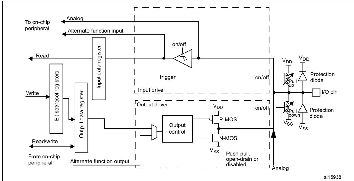
Figure 72. Basic structure of a 5-Volt tolerant I/O port bit
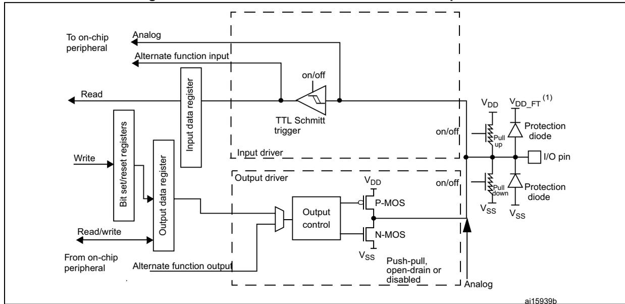
- 1. \( V_{DD\_FT} \) is a potential specific to 5-Volt tolerant I/Os and different from \( V_{DD} \) .
| MODE(i) [1:0] | OTYPER(i) | OSPEED(i) [1:0] | PUPD(i) | I/O configuration | |||
|---|---|---|---|---|---|---|---|
| [1:0] | [1:0] | ||||||
| 01 | 0 | SPEED [1:0] | 0 | 0 | GP output | PP | |
| 0 | 0 | 1 | GP output | PP + PU | |||
| 0 | 1 | 0 | GP output | PP + PD | |||
| 0 | 1 | 1 | Reserved | ||||
| 1 | 0 | 0 | GP output | OD | |||
| 1 | 0 | 1 | GP output | OD + PU | |||
| 1 | 1 | 0 | GP output | OD + PD | |||
| 1 | 1 | 1 | Reserved (GP output OD) | ||||
| 10 | 0 | SPEED [1:0] | 0 | 0 | AF | PP | |
| 0 | 0 | 1 | AF | PP + PU | |||
| 0 | 1 | 0 | AF | PP + PD | |||
| 0 | 1 | 1 | Reserved | ||||
| 1 | 0 | 0 | AF | OD | |||
| 1 | 0 | 1 | AF | OD + PU | |||
| 1 | 1 | 0 | AF | OD + PD | |||
| 1 | 1 | 1 | Reserved | ||||
| 00 | x | x | x | 0 | 0 | Input | Floating |
| x | x | x | 0 | 1 | Input | PU | |
| x | x | x | 1 | 0 | Input | PD | |
| x | x | x | 1 | 1 | Reserved (input floating) | ||
| 11 | x | x | x | 0 | 0 | Input/output | Analog |
| x | x | x | 0 | 1 | Reserved | ||
| x | x | x | 1 | 0 | |||
| x | x | x | 1 | 1 | |||
- 1. GP = general-purpose, PP = push-pull, PU = pull-up, PD = pull-down, OD = open-drain, AF = alternate function.
11.3.1 General-purpose I/O (GPIO)
During and just after reset, the alternate functions are not active and most of the I/O ports are configured in analog mode.
The debug pins are in AF pull-up/pull-down after reset:
- • PA15: JTDI in pull-up
- • PA14: JTCK/SWCLK in pull-down
- • PA13: JTMS/SWDAT in pull-up
- • PB4: NJTRST in pull-up
- • PB3: JTDO in floating state
When the pin is configured as output, the value written to the output data register (GPIOx_ODR) is output on the I/O pin. It is possible to use the output driver in push-pull mode or open-drain mode (only the low level is driven, high level is HI-Z).
The input data register (GPIOx_IDR) captures the data present on the I/O pin at every AHB clock cycle.
All GPIO pins have weak internal pull-up and pull-down resistors, which can be activated or not depending on the value in the GPIOx_PUPDR register.
11.3.2 I/O pin alternate function multiplexer and mapping
The device I/O pins are connected to on-board peripherals/modules through a multiplexer that allows only one peripheral alternate function (AF) connected to an I/O pin at a time. In this way, there can be no conflict between peripherals available on the same I/O pin.
Each I/O pin has a multiplexer with up to sixteen alternate function inputs (AF0 to AF15) that can be configured through the GPIOx_AFRL (for pin 0 to 7) and GPIOx_AFRH (for pin 8 to 15) registers:
- • After reset the multiplexer selection is alternate function 0 (AF0). The I/Os are configured in alternate function mode through GPIOx_MODER register.
- • The specific alternate function assignments for each pin are detailed in the device datasheet.
- • Cortex-M7 with FPU EVENTOUT is mapped on AF15
In addition to this flexible I/O multiplexing architecture, each peripheral has alternate functions mapped onto different I/O pins to optimize the number of peripherals available in smaller packages.
To use an I/O in a given configuration, the user has to proceed as follows:
- • Debug function: after each device reset these pins are assigned as alternate function pins immediately usable by the debugger host
- • System function: MCOx pins have to be configured in alternate function mode.
- • GPIO: configure the desired I/O as output, input or analog in the GPIOx_MODER register.
- •
Peripheral alternate function:
- – Connect the I/O to the desired AFx in one of the GPIOx_AFRL or GPIOx_AFRH register.
- – Select the type, pull-up/pull-down and output speed via the GPIOx_OTYPER, GPIOx_PUPDR and GPIOx_OSPEEDER registers, respectively.
- – Configure the desired I/O as an alternate function in the GPIOx_MODER register.
- •
Additional functions:
- – For the ADC and DAC, configure the desired I/O in analog mode in the GPIOx_MODER register and configure the required function in the ADC and DAC registers.
- – For the additional functions like RTC_OUT, RTC_TS, RTC_TAMPx, WKUPx and oscillators, configure the required function in the related RTC, PWR and RCC registers. These functions have priority over the configuration in the standard GPIO registers. For details about I/O control by the RTC, refer to Section 51.4: RTC functional description on page 1944 .
- •
EVENTOUT
- – Configure the I/O pin used to output the core EVENTOUT signal by connecting it to AF15.
Refer to the “Alternate function mapping” table in the device datasheet for the detailed mapping of the alternate function I/O pins.
11.3.3 I/O port control registers
Each of the GPIO ports has four 32-bit memory-mapped control registers (GPIOx_MODER, GPIOx_OTYPER, GPIOx_OSPEEDR, GPIOx_PUPDR) to configure up to 16 I/Os. The GPIOx_MODER register is used to select the I/O mode (input, output, AF, analog). The GPIOx_OTYPER and GPIOx_OSPEEDR registers are used to select the output type (push-pull or open-drain) and speed. The GPIOx_PUPDR register is used to select the pull-up/pull-down whatever the I/O direction.
11.3.4 I/O port data registers
Each GPIO has two 16-bit memory-mapped data registers: input and output data registers (GPIOx_IDR and GPIOx_ODR). GPIOx_ODR stores the data to be output, it is read/write accessible. The data input through the I/O are stored into the input data register (GPIOx_IDR), a read-only register.
See Section 11.4.5: GPIO port input data register (GPIOx_IDR) (x = A to H, J, K) and Section 11.4.6: GPIO port output data register (GPIOx_ODR) (x = A to H, J, K) for the register descriptions.
11.3.5 I/O data bitwise handling
The bit set reset register (GPIOx_BSRR) is a 32-bit register which allows the application to set and reset each individual bit in the output data register (GPIOx_ODR). The bit set reset register has twice the size of GPIOx_ODR.
To each bit in GPIOx_ODR, correspond two control bits in GPIOx_BSRR: BS(i) and BR(i). When written to 1, bit BS(i) sets the corresponding ODR(i) bit. When written to 1, bit BR(i) resets the ODR(i) corresponding bit.
Writing any bit to 0 in GPIOx_BSRR does not have any effect on the corresponding bit in GPIOx_ODR. If there is an attempt to both set and reset a bit in GPIOx_BSRR, the set action takes priority.
Using the GPIOx_BSRR register to change the values of individual bits in GPIOx_ODR is a “one-shot” effect that does not lock the GPIOx_ODR bits. The GPIOx_ODR bits can always
be accessed directly. The GPIOx_BSRR register provides a way of performing atomic bitwise handling.
There is no need for the software to disable interrupts when programming the GPIOx_ODR at bit level: it is possible to modify one or more bits in a single atomic AHB write access.
11.3.6 GPIO locking mechanism
It is possible to freeze the GPIO control registers by applying a specific write sequence to the GPIOx_LCKR register. The frozen registers are GPIOx_MODER, GPIOx_OTYPER, GPIOx_OSPEEDR, GPIOx_PUPDR, GPIOx_AFR and GPIOx_AFRH.
To write the GPIOx_LCKR register, a specific write / read sequence has to be applied. When the right LOCK sequence is applied to bit 16 in this register, the value of LCKR[15:0] is used to lock the configuration of the I/Os (during the write sequence the LCKR[15:0] value must be the same). When the LOCK sequence has been applied to a port bit, the value of the port bit can no longer be modified until the next MCU reset or peripheral reset. Each GPIOx_LCKR bit freezes the corresponding bit in the control registers (GPIOx_MODER, GPIOx_OTYPER, GPIOx_OSPEEDR, GPIOx_PUPDR, GPIOx_AFR and GPIOx_AFRH).
The LOCK sequence (refer to Section 11.4.8: GPIO port configuration lock register (GPIOx_LCKR) ( x = A to H, J, K )) can only be performed using a word (32-bit long) access to the GPIOx_LCKR register due to the fact that GPIOx_LCKR bit 16 has to be set at the same time as the [15:0] bits.
For more details refer to LCKR register description in Section 11.4.8: GPIO port configuration lock register (GPIOx_LCKR) ( x = A to H, J, K ).
11.3.7 I/O alternate function input/output
Two registers are provided to select one of the alternate function inputs/outputs available for each I/O. With these registers, the user can connect an alternate function to some other pin as required by the application.
This means that a number of possible peripheral functions are multiplexed on each GPIO using the GPIOx_AFR and GPIOx_AFRH alternate function registers. The application can thus select any one of the possible functions for each I/O. The AF selection signal being common to the alternate function input and alternate function output, a single channel is selected for the alternate function input/output of a given I/O.
To know which functions are multiplexed on each GPIO pin refer to the device datasheet.
11.3.8 External interrupt/wakeup lines
All ports have external interrupt capability. To use external interrupt lines, the port must be configured in input mode.
Refer to Section 20: Extended interrupt and event controller (EXTI) and to Section 20.3: EXTI functional description .
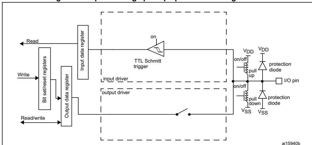
11.3.9 Input configuration
When the I/O port is programmed as input:
- • The output buffer is disabled
- • The Schmitt trigger input is activated
- • The pull-up and pull-down resistors are activated depending on the value in the GPIOx_PUPDR register
- • The data present on the I/O pin are sampled into the input data register every AHB clock cycle
- • A read access to the input data register provides the I/O state
Figure 73 shows the input configuration of the I/O port bit.
Figure 73. Input floating / pull up / pull down configurations
11.3.10 Output configuration
When the I/O port is programmed as output:
- • The output buffer is enabled:
- – Open drain mode: A “0” in the Output register activates the N-MOS whereas a “1” in the Output register leaves the port in Hi-Z (the P-MOS is never activated)
- – Push-pull mode: A “0” in the Output register activates the N-MOS whereas a “1” in the Output register activates the P-MOS
- • The Schmitt trigger input is activated
- • The pull-up and pull-down resistors are activated depending on the value in the GPIOx_PUPDR register
- • The data present on the I/O pin are sampled into the input data register every AHB clock cycle
- • A read access to the input data register gets the I/O state
- • A read access to the output data register gets the last written value
Figure 74 shows the output configuration of the I/O port bit.
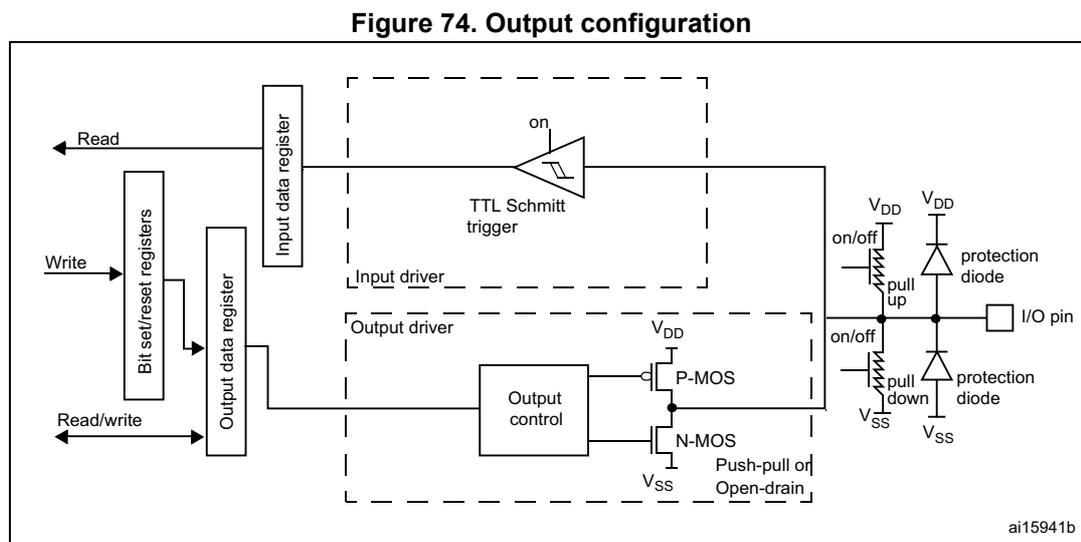
Figure 74. Output configuration
The diagram illustrates the internal architecture of an I/O port bit. On the left, external signals 'Read', 'Write', and 'Read/write' are shown. 'Read' connects to the 'Input data register'. 'Write' connects to 'Bit set/reset registers', which in turn connect to the 'Output data register'. 'Read/write' also connects to the 'Output data register'. The 'Input data register' feeds into an 'Input driver' containing a 'TTL Schmitt trigger'. The 'Output data register' feeds into an 'Output control' block, which drives a 'P-MOS' and an 'N-MOS' transistor. These transistors are part of an 'Output driver' and can be configured for 'Push-pull or Open-drain' mode. The transistors are connected to an 'I/O pin'. The pin is also connected to 'pull up' and 'pull down' resistors (with 'on/off' switches) and 'protection diode' structures connected to V DD and V SS . The entire internal circuitry is enclosed in a dashed box. The identifier 'ai15941b' is in the bottom right corner.
11.3.11 I/O compensation cell
This cell is used to control the I/O commutation slew rate (t fall / t rise ) to reduce the I/O noise on power supply.
The cell is split into two blocks:
- • The first block provides an optimal code for the current PVT. The code stored in this block can be read when the READY flag of the SYSCFG_CCSR is set.
- • The second block controls the I/O slew rate. The user selects the code to be applied and programs it by software.
The I/O compensation cell features 2 voltage ranges: 1.62 to 2.0 V and 2.7 to 3.6 V.
11.3.12 Alternate function configuration
When the I/O port is programmed as alternate function:
- • The output buffer can be configured in open-drain or push-pull mode
- • The output buffer is driven by the signals coming from the peripheral (transmitter enable and data)
- • The Schmitt trigger input is activated
- • The weak pull-up and pull-down resistors are activated or not depending on the value in the GPIOx_PUPDR register
- • The data present on the I/O pin are sampled into the input data register every AHB clock cycle
- • A read access to the input data register gets the I/O state
Figure 75 shows the alternate function configuration of the I/O port bit.
Figure 75. Alternate function configuration
11.3.13 Analog configuration
When the I/O port is programmed as analog configuration:
- • The output buffer is disabled
- • The Schmitt trigger input is deactivated, providing zero consumption for every analog value of the I/O pin. The output of the Schmitt trigger is forced to a constant value (0).
- • The weak pull-up and pull-down resistors are disabled by hardware
- • Read access to the input data register gets the value “0”
Figure 76 shows the high-impedance, analog-input configuration of the I/O port bits.
Figure 76. High impedance-analog configuration
Some pins/balls are directly connected to PA0_C, PA1_C, PC2_C and PC3_C ADC analog inputs (see Figure 77 ): there is a direct path between Pxy_C and Pxy pins/balls, through an analog switch (refer to Section 12.4.1: SYSCFG peripheral mode configuration register (SYSCFG_PMCR) for details on how to configure analog switches).
Figure 77. Analog inputs connected to ADC inputs
![Figure 77: Analog inputs connected to ADC inputs. This block diagram illustrates the internal architecture of a GPIO pin. On the left, various input and output sources are shown: 'To ADC', 'To on-chip peripherals' (Alternate Function Input), 'Read' (from Input data register), 'Write' (to Bit Set/Reset register), 'Read / Write' (to Output data register), 'Alternate Function Output' (from on-chip peripherals), and 'Analog' (from analog peripherals). The central part of the diagram shows the internal components: an 'Input Driver' containing a Schmitt Trigger and an 'Output Driver' containing an OUTPUT CONTROL block. The Input Driver is connected to an 'Input data register' and an 'On/off' switch controlled by 'MODERy [1:0] in GPIOx_MODER (reset state: open)'. The Output Driver is connected to 'Bit Set/Reset register' and 'Output data register'. On the right, the pin is shown with its internal connections to VDD, VSS, and pull-up/pull-down resistors. A note indicates that the switch default state depends on the PxySO bit Reset value in SYSCFG_PMCR. Pins PA0_C, PA1_C, PC2_C, and PC3_C are shown connected to the ADC input path. The diagram is labeled MSv41921V3.](/RM0468-STM32H723-733-725-735-730/7f7e4fb8ab2537d83350881b7ae97b7f_img.jpg)
- 1. VDD_FT is a potential specific to 5V tolerant I/Os. It is distinct from VDD.
11.3.14 Using the HSE or LSE oscillator pins as GPIOs
When the HSE or LSE oscillator is switched OFF (default state after reset), the related oscillator pins can be used as normal GPIOs.
When the HSE or LSE oscillator is switched ON (by setting the HSEON or LSEON bit in the RCC_CSR register) the oscillator takes control of its associated pins and the GPIO configuration of these pins has no effect.
When the oscillator is configured in a user external clock mode, only the OSC_IN or OSC32_IN pin is reserved for clock input and the OSC_OUT or OSC32_OUT pin can still be used as normal GPIO.
11.3.15 Using the GPIO pins in the backup supply domain
The PC13/PC14/PC15 GPIO functionality is lost when the core supply domain is powered off (when the device enters Standby mode). In this case, if their GPIO configuration is not bypassed by the RTC configuration, these pins are set in an analog input mode.
11.4 GPIO registers
For a summary of register bits, register address offsets and reset values, refer to Table 90 .
The peripheral registers can be written in word, half word or byte mode.
11.4.1 GPIO port mode register (GPIOx_MODER)
(x = A to H, J, K)
Address offset: 0x00
Reset value: 0xABFF FFFF for port A
Reset value: 0xFFFF FEBF for port B
Reset value: 0x00FF 0000 for port J
Reset value: 0x0000 003F for port K
Reset value: 0xFFFF FFFF for other ports
| 31 | 30 | 29 | 28 | 27 | 26 | 25 | 24 | 23 | 22 | 21 | 20 | 19 | 18 | 17 | 16 |
|---|---|---|---|---|---|---|---|---|---|---|---|---|---|---|---|
| MODER15[1:0] | MODER14[1:0] | MODER13[1:0] | MODER12[1:0] | MODER11[1:0] | MODER10[1:0] | MODER9[1:0] | MODER8[1:0] | ||||||||
| rw | rw | rw | rw | rw | rw | rw | rw | rw | rw | rw | rw | rw | rw | rw | rw |
| 15 | 14 | 13 | 12 | 11 | 10 | 9 | 8 | 7 | 6 | 5 | 4 | 3 | 2 | 1 | 0 |
| MODER7[1:0] | MODER6[1:0] | MODER5[1:0] | MODER4[1:0] | MODER3[1:0] | MODER2[1:0] | MODER1[1:0] | MODER0[1:0] | ||||||||
| rw | rw | rw | rw | rw | rw | rw | rw | rw | rw | rw | rw | rw | rw | rw | rw |
Bits 31:0 MODER[15:0][1:0] : Port x configuration I/O pin y (y = 15 to 0)
These bits are written by software to configure the I/O mode.
- 00: Input mode
- 01: General purpose output mode
- 10: Alternate function mode
- 11: Analog mode (reset state)
11.4.2 GPIO port output type register (GPIOx_OTYPER)
(x = A to H, J, K)
Address offset: 0x04
Reset value: 0x0000 0000
| 31 | 30 | 29 | 28 | 27 | 26 | 25 | 24 | 23 | 22 | 21 | 20 | 19 | 18 | 17 | 16 |
|---|---|---|---|---|---|---|---|---|---|---|---|---|---|---|---|
| Res. | Res. | Res. | Res. | Res. | Res. | Res. | Res. | Res. | Res. | Res. | Res. | Res. | Res. | Res. | Res. |
| 15 | 14 | 13 | 12 | 11 | 10 | 9 | 8 | 7 | 6 | 5 | 4 | 3 | 2 | 1 | 0 |
| OT15 | OT14 | OT13 | OT12 | OT11 | OT10 | OT9 | OT8 | OT7 | OT6 | OT5 | OT4 | OT3 | OT2 | OT1 | OT0 |
| rw | rw | rw | rw | rw | rw | rw | rw | rw | rw | rw | rw | rw | rw | rw | rw |
Bits 31:16 Reserved, must be kept at reset value.
Bits 15:0 OT[15:0] : Port x configuration I/O pin y (y = 15 to 0)
These bits are written by software to configure the I/O output type.
0: Output push-pull (reset state)
1: Output open-drain
11.4.3 GPIO port output speed register (GPIOx_OSPEEDR)
(x = A to H, J, K)
Address offset: 0x08
Reset value: 0x0C00 0000 (for port A)
Reset value: 0x0000 00C0 (for port B)
Reset value: 0x0000 0000 (for other ports)
| 31 | 30 | 29 | 28 | 27 | 26 | 25 | 24 | 23 | 22 | 21 | 20 | 19 | 18 | 17 | 16 |
|---|---|---|---|---|---|---|---|---|---|---|---|---|---|---|---|
| OSPEEDR15 [1:0] | OSPEEDR14 [1:0] | OSPEEDR13 [1:0] | OSPEEDR12 [1:0] | OSPEEDR11 [1:0] | OSPEEDR10 [1:0] | OSPEEDR9 [1:0] | OSPEEDR8 [1:0] | ||||||||
| rw | rw | rw | rw | rw | rw | rw | rw | rw | rw | rw | rw | rw | rw | rw | rw |
| 15 | 14 | 13 | 12 | 11 | 10 | 9 | 8 | 7 | 6 | 5 | 4 | 3 | 2 | 1 | 0 |
|---|---|---|---|---|---|---|---|---|---|---|---|---|---|---|---|
| OSPEEDR7 [1:0] | OSPEEDR6 [1:0] | OSPEEDR5 [1:0] | OSPEEDR4 [1:0] | OSPEEDR3 [1:0] | OSPEEDR2 [1:0] | OSPEEDR1 [1:0] | OSPEEDR0 [1:0] | ||||||||
| rw | rw | rw | rw | rw | rw | rw | rw | rw | rw | rw | rw | rw | rw | rw | rw |
Bits 31:0 OSPEEDR[15:0][1:0] : Port x configuration I/O pin y (y = 15 to 0)
These bits are written by software to configure the I/O output speed.
00: Low speed
01: Medium speed
10: High speed
11: Very high speed
Note: Refer to the product datasheets for the values of OSPEEDRy bits versus V DD range and external load.
11.4.4 GPIO port pull-up/pull-down register (GPIOx_PUPDR)
(x = A to H, J, K)
Address offset: 0x0C
Reset value: 0x6400 0000 (for port A)
Reset value: 0x0000 0100 (for port B)
Reset value: 0x0000 0000 (for other ports)
| 31 | 30 | 29 | 28 | 27 | 26 | 25 | 24 | 23 | 22 | 21 | 20 | 19 | 18 | 17 | 16 |
|---|---|---|---|---|---|---|---|---|---|---|---|---|---|---|---|
| PUPDR15[1:0] | PUPDR14[1:0] | PUPDR13[1:0] | PUPDR12[1:0] | PUPDR11[1:0] | PUPDR10[1:0] | PUPDR9[1:0] | PUPDR8[1:0] | ||||||||
| rw | rw | rw | rw | rw | rw | rw | rw | rw | rw | rw | rw | rw | rw | rw | rw |
| 15 | 14 | 13 | 12 | 11 | 10 | 9 | 8 | 7 | 6 | 5 | 4 | 3 | 2 | 1 | 0 |
|---|---|---|---|---|---|---|---|---|---|---|---|---|---|---|---|
| PUPDR7[1:0] | PUPDR6[1:0] | PUPDR5[1:0] | PUPDR4[1:0] | PUPDR3[1:0] | PUPDR2[1:0] | PUPDR1[1:0] | PUPDR0[1:0] | ||||||||
| rw | rw | rw | rw | rw | rw | rw | rw | rw | rw | rw | rw | rw | rw | rw | rw |
Bits 31:0 PUPDR[15:0][1:0] : Port x configuration I/O pin y (y = 15 to 0)
These bits are written by software to configure the I/O pull-up or pull-down
00: No pull-up, pull-down
01: Pull-up
10: Pull-down
11: Reserved
11.4.5 GPIO port input data register (GPIOx_IDR)
(x = A to H, J, K)
Address offset: 0x10
Reset value: 0x0000 XXXX
| 31 | 30 | 29 | 28 | 27 | 26 | 25 | 24 | 23 | 22 | 21 | 20 | 19 | 18 | 17 | 16 |
|---|---|---|---|---|---|---|---|---|---|---|---|---|---|---|---|
| Res. | Res. | Res. | Res. | Res. | Res. | Res. | Res. | Res. | Res. | Res. | Res. | Res. | Res. | Res. | Res. |
| 15 | 14 | 13 | 12 | 11 | 10 | 9 | 8 | 7 | 6 | 5 | 4 | 3 | 2 | 1 | 0 |
| IDR15 | IDR14 | IDR13 | IDR12 | IDR11 | IDR10 | IDR9 | IDR8 | IDR7 | IDR6 | IDR5 | IDR4 | IDR3 | IDR2 | IDR1 | IDR0 |
| r | r | r | r | r | r | r | r | r | r | r | r | r | r | r | r |
Bits 31:16 Reserved, must be kept at reset value.
Bits 15:0 IDR[15:0] : Port x input data I/O pin y (y = 15 to 0)
These bits are read-only. They contain the input value of the corresponding I/O port.
11.4.6 GPIO port output data register (GPIOx_ODR)
(x = A to H, J, K)
Address offset: 0x14
Reset value: 0x0000 0000
| 31 | 30 | 29 | 28 | 27 | 26 | 25 | 24 | 23 | 22 | 21 | 20 | 19 | 18 | 17 | 16 |
|---|---|---|---|---|---|---|---|---|---|---|---|---|---|---|---|
| Res. | Res. | Res. | Res. | Res. | Res. | Res. | Res. | Res. | Res. | Res. | Res. | Res. | Res. | Res. | Res. |
| 15 | 14 | 13 | 12 | 11 | 10 | 9 | 8 | 7 | 6 | 5 | 4 | 3 | 2 | 1 | 0 |
| ODR15 | ODR14 | ODR13 | ODR12 | ODR11 | ODR10 | ODR9 | ODR8 | ODR7 | ODR6 | ODR5 | ODR4 | ODR3 | ODR2 | ODR1 | ODR0 |
| rw | rw | rw | rw | rw | rw | rw | rw | rw | rw | rw | rw | rw | rw | rw | rw |
Bits 31:16 Reserved, must be kept at reset value.
Bits 15:0 ODR[15:0] : Port output data I/O pin y (y = 15 to 0)
These bits can be read and written by software.
Note: For atomic bit set/reset, the ODR bits can be individually set and/or reset by writing to the GPIOx_BSRR register (x = A to H, J, K).
11.4.7 GPIO port bit set/reset register (GPIOx_BSRR)
(x = A to H, J, K)
Address offset: 0x18
Reset value: 0x0000 0000
| 31 | 30 | 29 | 28 | 27 | 26 | 25 | 24 | 23 | 22 | 21 | 20 | 19 | 18 | 17 | 16 |
|---|---|---|---|---|---|---|---|---|---|---|---|---|---|---|---|
| BR15 | BR14 | BR13 | BR12 | BR11 | BR10 | BR9 | BR8 | BR7 | BR6 | BR5 | BR4 | BR3 | BR2 | BR1 | BR0 |
| w | w | w | w | w | w | w | w | w | w | w | w | w | w | w | w |
| 15 | 14 | 13 | 12 | 11 | 10 | 9 | 8 | 7 | 6 | 5 | 4 | 3 | 2 | 1 | 0 |
| BS15 | BS14 | BS13 | BS12 | BS11 | BS10 | BS9 | BS8 | BS7 | BS6 | BS5 | BS4 | BS3 | BS2 | BS1 | BS0 |
| w | w | w | w | w | w | w | w | w | w | w | w | w | w | w | w |
Bits 31:16 BR[15:0] : Port x reset I/O pin y (y = 15 to 0)
These bits are write-only. A read to these bits returns the value 0x0000.
0: No action on the corresponding ODRx bit
1: Resets the corresponding ODRx bit
Note: If both BSx and BRx are set, BSx has priority.
Bits 15:0 BS[15:0] : Port x set I/O pin y (y = 15 to 0)
These bits are write-only. A read to these bits returns the value 0x0000.
0: No action on the corresponding ODRx bit
1: Sets the corresponding ODRx bit
11.4.8 GPIO port configuration lock register (GPIOx_LCKR)
(x = A to H, J, K)
This register is used to lock the configuration of the port bits when a correct write sequence is applied to bit 16 (LCKK). The value of bits [15:0] is used to lock the configuration of the GPIO. During the write sequence, the value of LCKR[15:0] must not change. When the LOCK sequence has been applied on a port bit, the value of this port bit can no longer be modified until the next MCU reset or peripheral reset.
Note: A specific write sequence is used to write to the GPIOx_LCKR register. Only word access (32-bit long) is allowed during this locking sequence.
Each lock bit freezes a specific configuration register (control and alternate function registers).
Address offset: 0x1C
Reset value: 0x0000 0000
| 31 | 30 | 29 | 28 | 27 | 26 | 25 | 24 | 23 | 22 | 21 | 20 | 19 | 18 | 17 | 16 |
|---|---|---|---|---|---|---|---|---|---|---|---|---|---|---|---|
| Res. | Res. | Res. | Res. | Res. | Res. | Res. | Res. | Res. | Res. | Res. | Res. | Res. | Res. | Res. | LCKK |
| rw | |||||||||||||||
| 15 | 14 | 13 | 12 | 11 | 10 | 9 | 8 | 7 | 6 | 5 | 4 | 3 | 2 | 1 | 0 |
| LCK15 | LCK14 | LCK13 | LCK12 | LCK11 | LCK10 | LCK9 | LCK8 | LCK7 | LCK6 | LCK5 | LCK4 | LCK3 | LCK2 | LCK1 | LCK0 |
| rw | rw | rw | rw | rw | rw | rw | rw | rw | rw | rw | rw | rw | rw | rw | rw |
Bits 31:17 Reserved, must be kept at reset value.
Bit 16 LCKK : Lock key
This bit can be read any time. It can only be modified using the lock key write sequence.
0: Port configuration lock key not active
1: Port configuration lock key active. The GPIOx_LCKR register is locked until the next MCU reset or peripheral reset.
LOCK key write sequence:
WR LCKR[16] = 1 + LCKR[15:0]
WR LCKR[16] = 0 + LCKR[15:0]
WR LCKR[16] = 1 + LCKR[15:0]
RD LCKR
RD LCKR[16] = 1 (this read operation is optional but it confirms that the lock is active)
Note: During the LOCK key write sequence, the value of LCK[15:0] must not change.
Any error in the lock sequence aborts the lock.
After the first lock sequence on any bit of the port, any read access on the LCKK bit returns 1 until the next MCU reset or peripheral reset.
Bits 15:0 LCK[15:0] : Port x lock I/O pin y (y = 15 to 0)
These bits are read/write but can only be written when the LCKK bit is 0.
0: Port configuration not locked
1: Port configuration locked
11.4.9 GPIO alternate function low register (GPIOx_AFRL)
(x = A to H, J, K)
Address offset: 0x20
Reset value: 0x0000 0000
| 31 | 30 | 29 | 28 | 27 | 26 | 25 | 24 | 23 | 22 | 21 | 20 | 19 | 18 | 17 | 16 |
|---|---|---|---|---|---|---|---|---|---|---|---|---|---|---|---|
| AFR7[3:0] | AFR6[3:0] | AFR5[3:0] | AFR4[3:0] | ||||||||||||
| rw | rw | rw | rw | rw | rw | rw | rw | rw | rw | rw | rw | rw | rw | rw | rw |
| 15 | 14 | 13 | 12 | 11 | 10 | 9 | 8 | 7 | 6 | 5 | 4 | 3 | 2 | 1 | 0 |
| AFR3[3:0] | AFR2[3:0] | AFR1[3:0] | AFR0[3:0] | ||||||||||||
| rw | rw | rw | rw | rw | rw | rw | rw | rw | rw | rw | rw | rw | rw | rw | rw |
Bits 31:0 AFR[7:0][3:0] : Alternate function selection for port x I/O pin y (y = 7 to 0)
These bits are written by software to configure alternate function I/Os.
0000: AF0
0001: AF1
0010: AF2
0011: AF3
0100: AF4
0101: AF5
0110: AF6
0111: AF7
1000: AF8
1001: AF9
1010: AF10
1011: AF11
1100: AF12
1101: AF13
1110: AF14
1111: AF15
11.4.10 GPIO alternate function high register (GPIOx_AFRH)
(x = A to H, J, K)
Address offset: 0x24
Reset value: 0x0000 0000
| 31 | 30 | 29 | 28 | 27 | 26 | 25 | 24 | 23 | 22 | 21 | 20 | 19 | 18 | 17 | 16 |
|---|---|---|---|---|---|---|---|---|---|---|---|---|---|---|---|
| AFR15[3:0] | AFR14[3:0] | AFR13[3:0] | AFR12[3:0] | ||||||||||||
| rw | rw | rw | rw | rw | rw | rw | rw | rw | rw | rw | rw | rw | rw | rw | rw |
| 15 | 14 | 13 | 12 | 11 | 10 | 9 | 8 | 7 | 6 | 5 | 4 | 3 | 2 | 1 | 0 |
| AFR11[3:0] | AFR10[3:0] | AFR9[3:0] | AFR8[3:0] | ||||||||||||
| rw | rw | rw | rw | rw | rw | rw | rw | rw | rw | rw | rw | rw | rw | rw | rw |
Bits 31:0 AFR[15:8][3:0] : Alternate function selection for port x I/O pin y (y = 15 to 8)
These bits are written by software to configure alternate function I/Os.
0000: AF0
0001: AF1
0010: AF2
0011: AF3
0100: AF4
0101: AF5
0110: AF6
0111: AF7
1000: AF8
1001: AF9
1010: AF10
1011: AF11
1100: AF12
1101: AF13
1110: AF14
1111: AF15
11.4.11 GPIO register map
The following table gives the GPIO register map and reset values.
Table 90. GPIO register map and reset values
| Offset | Register name | 31 | 30 | 29 | 28 | 27 | 26 | 25 | 24 | 23 | 22 | 21 | 20 | 19 | 18 | 17 | 16 | 15 | 14 | 13 | 12 | 11 | 10 | 9 | 8 | 7 | 6 | 5 | 4 | 3 | 2 | 1 | 0 |
|---|---|---|---|---|---|---|---|---|---|---|---|---|---|---|---|---|---|---|---|---|---|---|---|---|---|---|---|---|---|---|---|---|---|
| 0x00 | GPIOA_MODER | MODER15[1:0] | MODER14[1:0] | MODER13[1:0] | MODER12[1:0] | MODER11[1:0] | MODER10[1:0] | MODER9[1:0] | MODER8[1:0] | MODER7[1:0] | MODER6[1:0] | MODER5[1:0] | MODER4[1:0] | MODER3[1:0] | MODER2[1:0] | MODER1[1:0] | MODER0[1:0] | ||||||||||||||||
| Reset value | 1 | 0 | 1 | 0 | 1 | 0 | 1 | 1 | 1 | 1 | 1 | 1 | 1 | 1 | 1 | 1 | 1 | 1 | 1 | 1 | 1 | 1 | 1 | 1 | 1 | 1 | 1 | 1 | 1 | 1 | 1 | 1 | |
| 0x00 | GPIOB_MODER | MODER15[1:0] | MODER14[1:0] | MODER13[1:0] | MODER12[1:0] | MODER11[1:0] | MODER10[1:0] | MODER9[1:0] | MODER8[1:0] | MODER7[1:0] | MODER6[1:0] | MODER5[1:0] | MODER4[1:0] | MODER3[1:0] | MODER2[1:0] | MODER1[1:0] | MODER0[1:0] | ||||||||||||||||
| Reset value | 1 | 1 | 1 | 1 | 1 | 1 | 1 | 1 | 1 | 1 | 1 | 1 | 1 | 1 | 1 | 1 | 1 | 1 | 1 | 1 | 1 | 1 | 1 | 0 | 1 | 0 | 1 | 1 | 1 | 1 | 1 | 1 | |
| 0x00 | GPIOx_MODER (where x = C..H) | MODER15[1:0] | MODER14[1:0] | MODER13[1:0] | MODER12[1:0] | MODER11[1:0] | MODER10[1:0] | MODER9[1:0] | MODER8[1:0] | MODER7[1:0] | MODER6[1:0] | MODER5[1:0] | MODER4[1:0] | MODER3[1:0] | MODER2[1:0] | MODER1[1:0] | MODER0[1:0] | ||||||||||||||||
| Reset value | 1 | 1 | 1 | 1 | 1 | 1 | 1 | 1 | 1 | 1 | 1 | 1 | 1 | 1 | 1 | 1 | 1 | 1 | 1 | 1 | 1 | 1 | 1 | 1 | 1 | 1 | 1 | 1 | 1 | 1 | 1 | 1 | |
| 0x00 | GPIOJ_MODER | MODER15[1:0] | MODER14[1:0] | MODER13[1:0] | MODER12[1:0] | MODER11[1:0] | MODER10[1:0] | MODER9[1:0] | MODER8[1:0] | MODER7[1:0] | MODER6[1:0] | MODER5[1:0] | MODER4[1:0] | MODER3[1:0] | MODER2[1:0] | MODER1[1:0] | MODER0[1:0] | ||||||||||||||||
| Reset value | 0 | 0 | 0 | 0 | 0 | 0 | 0 | 0 | 1 | 1 | 1 | 1 | 1 | 1 | 1 | 1 | 0 | 0 | 0 | 0 | 0 | 0 | 0 | 0 | 0 | 0 | 0 | 0 | 0 | 0 | 0 | 0 | |
| 0x00 | GPIOK_MODER | MODER15[1:0] | MODER14[1:0] | MODER13[1:0] | MODER12[1:0] | MODER11[1:0] | MODER10[1:0] | MODER9[1:0] | MODER8[1:0] | MODER7[1:0] | MODER6[1:0] | MODER5[1:0] | MODER4[1:0] | MODER3[1:0] | MODER2[1:0] | MODER1[1:0] | MODER0[1:0] | ||||||||||||||||
| Reset value | 0 | 0 | 0 | 0 | 0 | 0 | 0 | 0 | 0 | 0 | 0 | 0 | 0 | 0 | 0 | 0 | 0 | 0 | 0 | 0 | 0 | 0 | 0 | 0 | 0 | 0 | 1 | 1 | 1 | 1 | 1 | 1 | |
| 0x04 | GPIOx_OTYPER (where x = A to H, J, K) | Res. | Res. | Res. | Res. | Res. | Res. | Res. | Res. | Res. | Res. | Res. | Res. | Res. | Res. | Res. | Res. | OT15 | OT14 | OT13 | OT12 | OT11 | OT10 | OT9 | OT8 | OT7 | OT6 | OT5 | OT4 | OT3 | OT2 | OT1 | OT0 |
| Reset value | 0 | 0 | 0 | 0 | 0 | 0 | 0 | 0 | 0 | 0 | 0 | 0 | 0 | 0 | 0 | 0 | |||||||||||||||||
| 0x08 | GPIOA_OSPEEDR | OSPEEDR15[1:0] | OSPEEDR14[1:0] | OSPEEDR13[1:0] | OSPEEDR12[1:0] | OSPEEDR11[1:0] | OSPEEDR10[1:0] | OSPEEDR9[1:0] | OSPEEDR8[1:0] | OSPEEDR7[1:0] | OSPEEDR6[1:0] | OSPEEDR5[1:0] | OSPEEDR4[1:0] | OSPEEDR3[1:0] | OSPEEDR2[1:0] | OSPEEDR1[1:0] | OSPEEDR0[1:0] | ||||||||||||||||
| Reset value | 0 | 0 | 0 | 0 | 1 | 1 | 0 | 0 | 0 | 0 | 0 | 0 | 0 | 0 | 0 | 0 | 0 | 0 | 0 | 0 | 0 | 0 | 0 | 0 | 0 | 0 | 0 | 0 | 0 | 0 | 0 | 0 | |
| 0x08 | GPIOB_OSPEEDR | OSPEEDR15[1:0] | OSPEEDR14[1:0] | OSPEEDR13[1:0] | OSPEEDR12[1:0] | OSPEEDR11[1:0] | OSPEEDR10[1:0] | OSPEEDR9[1:0] | OSPEEDR8[1:0] | OSPEEDR7[1:0] | OSPEEDR6[1:0] | OSPEEDR5[1:0] | OSPEEDR4[1:0] | OSPEEDR3[1:0] | OSPEEDR2[1:0] | OSPEEDR1[1:0] | OSPEEDR0[1:0] | ||||||||||||||||
| Reset value | 0 | 0 | 0 | 0 | 0 | 0 | 0 | 0 | 0 | 0 | 0 | 0 | 0 | 0 | 0 | 0 | 0 | 0 | 0 | 0 | 0 | 0 | 0 | 0 | 1 | 1 | 0 | 0 | 0 | 0 | 0 | 0 |
Table 90. GPIO register map and reset values (continued)
| Offset | Register name | 31 | 30 | 29 | 28 | 27 | 26 | 25 | 24 | 23 | 22 | 21 | 20 | 19 | 18 | 17 | 16 | 15 | 14 | 13 | 12 | 11 | 10 | 9 | 8 | 7 | 6 | 5 | 4 | 3 | 2 | 1 | 0 |
|---|---|---|---|---|---|---|---|---|---|---|---|---|---|---|---|---|---|---|---|---|---|---|---|---|---|---|---|---|---|---|---|---|---|
| 0x08 | GPIOx_OSPEEDR (where x = C..H, J, K) | OSPEEDR15[1:0] | OSPEEDR14[1:0] | OSPEEDR13[1:0] | OSPEEDR12[1:0] | OSPEEDR11[1:0] | OSPEEDR10[1:0] | OSPEEDR9[1:0] | OSPEEDR8[1:0] | OSPEEDR7[1:0] | OSPEEDR6[1:0] | OSPEEDR5[1:0] | OSPEEDR4[1:0] | OSPEEDR3[1:0] | OSPEEDR2[1:0] | OSPEEDR1[1:0] | OSPEEDR0[1:0] | ||||||||||||||||
| Reset value | 0 | 0 | 0 | 0 | 0 | 0 | 0 | 0 | 0 | 0 | 0 | 0 | 0 | 0 | 0 | 0 | 0 | 0 | 0 | 0 | 0 | 0 | 0 | 0 | 0 | 0 | 0 | 0 | 0 | 0 | 0 | 0 | |
| 0x0C | GPIOA_PUPDR | PUPDR15[1:0] | PUPDR14[1:0] | PUPDR13[1:0] | PUPDR12[1:0] | PUPDR11[1:0] | PUPDR10[1:0] | PUPDR9[1:0] | PUPDR8[1:0] | PUPDR7[1:0] | PUPDR6[1:0] | PUPDR5[1:0] | PUPDR4[1:0] | PUPDR3[1:0] | PUPDR2[1:0] | PUPDR1[1:0] | PUPDR0[1:0] | ||||||||||||||||
| Reset value | 0 | 1 | 1 | 0 | 0 | 1 | 0 | 0 | 0 | 0 | 0 | 0 | 0 | 0 | 0 | 0 | 0 | 0 | 0 | 0 | 0 | 0 | 0 | 0 | 0 | 0 | 0 | 0 | 0 | 0 | 0 | 0 | |
| 0x0C | GPIOB_PUPDR | PUPDR15[1:0] | PUPDR14[1:0] | PUPDR13[1:0] | PUPDR12[1:0] | PUPDR11[1:0] | PUPDR10[1:0] | PUPDR9[1:0] | PUPDR8[1:0] | PUPDR7[1:0] | PUPDR6[1:0] | PUPDR5[1:0] | PUPDR4[1:0] | PUPDR3[1:0] | PUPDR2[1:0] | PUPDR1[1:0] | PUPDR0[1:0] | ||||||||||||||||
| Reset value | 0 | 0 | 0 | 0 | 0 | 0 | 0 | 0 | 0 | 0 | 0 | 0 | 0 | 0 | 0 | 0 | 0 | 0 | 0 | 0 | 0 | 0 | 0 | 1 | 0 | 0 | 0 | 0 | 0 | 0 | 0 | 0 | |
| 0x0C | GPIOx_PUPDR (where x = C..H, J, K) | PUPDR15[1:0] | PUPDR14[1:0] | PUPDR13[1:0] | PUPDR12[1:0] | PUPDR11[1:0] | PUPDR10[1:0] | PUPDR9[1:0] | PUPDR8[1:0] | PUPDR7[1:0] | PUPDR6[1:0] | PUPDR5[1:0] | PUPDR4[1:0] | PUPDR3[1:0] | PUPDR2[1:0] | PUPDR1[1:0] | PUPDR0[1:0] | ||||||||||||||||
| Reset value | 0 | 0 | 0 | 0 | 0 | 0 | 0 | 0 | 0 | 0 | 0 | 0 | 0 | 0 | 0 | 0 | 0 | 0 | 0 | 0 | 0 | 0 | 0 | 0 | 0 | 0 | 0 | 0 | 0 | 0 | 0 | 0 | |
| 0x10 | GPIOx_IDR (where x = A to H, J, K) | Res | Res | Res | Res | Res | Res | Res | Res | Res | Res | Res | Res | Res | Res | Res | Res | IDR15 | IDR14 | IDR13 | IDR12 | IDR11 | IDR10 | IDR9 | IDR8 | IDR7 | IDR6 | IDR5 | IDR4 | IDR3 | IDR2 | IDR1 | IDR0 |
| Reset value | x | x | x | x | x | x | x | x | x | x | x | x | x | x | x | x | |||||||||||||||||
| 0x14 | GPIOx_ODR (where x = A to H, J, K) | Res | Res | Res | Res | Res | Res | Res | Res | Res | Res | Res | Res | Res | Res | Res | Res | ODR15 | ODR14 | ODR13 | ODR12 | ODR11 | ODR10 | ODR9 | ODR8 | ODR7 | ODR6 | ODR5 | ODR4 | ODR3 | ODR2 | ODR1 | ODR0 |
| Reset value | 0 | 0 | 0 | 0 | 0 | 0 | 0 | 0 | 0 | 0 | 0 | 0 | 0 | 0 | 0 | 0 | |||||||||||||||||
| 0x18 | GPIOx_BSRR (where x = A to H, J, K) | BR15 | BR14 | BR13 | BR12 | BR11 | BR10 | BR9 | BR8 | BR7 | BR6 | BR5 | BR4 | BR3 | BR2 | BR1 | BR0 | BS15 | BS14 | BS13 | BS12 | BS11 | BS10 | BS9 | BS8 | BS7 | BS6 | BS5 | BS4 | BS3 | BS2 | BS1 | BS0 |
| Reset value | 0 | 0 | 0 | 0 | 0 | 0 | 0 | 0 | 0 | 0 | 0 | 0 | 0 | 0 | 0 | 0 | 0 | 0 | 0 | 0 | 0 | 0 | 0 | 0 | 0 | 0 | 0 | 0 | 0 | 0 | 0 | 0 | |
| 0x1C | GPIOx_LCKR (where x = A to H, J, K) | Res | Res | Res | Res | Res | Res | Res | Res | Res | Res | Res | Res | Res | Res | Res | Res | LCK15 | LCK14 | LCK13 | LCK12 | LCK11 | LCK10 | LCK9 | LCK8 | LCK7 | LCK6 | LCK5 | LCK4 | LCK3 | LCK2 | LCK1 | LCK0 |
| Reset value | 0 | 0 | 0 | 0 | 0 | 0 | 0 | 0 | 0 | 0 | 0 | 0 | 0 | 0 | 0 | 0 | |||||||||||||||||
| 0x20 | GPIOx_AFR (where x = A to H, J, K) | AFR7[3:0] | AFR6[3:0] | AFR5[3:0] | AFR4[3:0] | AFR3[3:0] | AFR2[3:0] | AFR1[3:0] | AFR0[3:0] | ||||||||||||||||||||||||
| Reset value | 0 | 0 | 0 | 0 | 0 | 0 | 0 | 0 | 0 | 0 | 0 | 0 | 0 | 0 | 0 | 0 | 0 | 0 | 0 | 0 | 0 | 0 | 0 | 0 | 0 | 0 | 0 | 0 | 0 | 0 | 0 | 0 | |
| 0x24 | GPIOx_AFRH (where x = A to H, J, K) | AFR15[3:0] | AFR14[3:0] | AFR13[3:0] | AFR12[3:0] | AFR11[3:0] | AFR10[3:0] | AFR9[3:0] | AFR8[3:0] | ||||||||||||||||||||||||
| Reset value | 0 | 0 | 0 | 0 | 0 | 0 | 0 | 0 | 0 | 0 | 0 | 0 | 0 | 0 | 0 | 0 | 0 | 0 | 0 | 0 | 0 | 0 | 0 | 0 | 0 | 0 | 0 | 0 | 0 | 0 | 0 | 0 | |