8. Reset and clock control (RCC)
The RCC block manages the clock and reset generation for the whole microcontroller.
The RCC block is located in the D3 domain (refer to Section 6: Power control (PWR) for a detailed description).
The operating modes this section refers to are defined in Section 6.6.1: Operating modes of the PWR block.
8.1 RCC main features
Reset block
- • Generation of local and system reset
- • Bidirectional pin reset allowing to reset the microcontroller or external devices
- • WWDG reset supported
Clock generation block
- • Generation and dispatching of clocks for the complete device
- • 3 separate PLLs using integer or fractional ratios
- • Possibility to change the PLL fractional ratios on-the-fly
- • Smart clock gating to reduce power dissipation
- • 2 external oscillators:
- – High-speed external oscillator (HSE) supporting a wide range of crystals from 4 to 50 MHz frequency
- – Low-speed external oscillator (LSE) for the 32 kHz crystals
- • 4 internal oscillators
- – High-speed internal oscillator (HSI)
- – 48 MHz RC oscillator (HSI48)
- – Low-power Internal oscillator (CSI)
- – Low-speed internal oscillator (LSI)
- • Buffered clock outputs for external devices
- • Generation of two types of interrupts lines:
- – Dedicated interrupt lines for clock security management
- – One general interrupt line for other events
- • Clock generation handling in Stop and Standby mode
- • D3 domain Autonomous mode
8.2 RCC block diagram
Figure 42 shows the RCC block diagram.
Figure 42. RCC Block diagram
The diagram illustrates the internal architecture of the RCC (Reset and Clock Control) block. At the top, the NRST pin is connected to a 'System Reset Control' block, which outputs 'nreset (system reset)' to all circuit blocks. Below this, 'Core Reset Control' blocks receive inputs from IWDG1, WWDG1, and 'rcc_sft_rst', outputting 'rcc_c_rst'. The 'Clock Manager (CMU)' is central, receiving various clock inputs and managing power and sleep states for the CPU and peripherals. The 'System Clock Generation (SCGU)' block uses oscillators (HSE/CSS, HSI48, LSI, HSI, CSI) and PLLs (PLL1, PLL2, PLL3) to generate system clocks. The 'Peripheral Kernel clock Selection (PKSU)' block selects clocks for peripherals like Ethernet, USB, and I2S. The 'Register Interface and Control' block is connected to the AHB Bus and handles interrupts (EXTI). External pins include NRST, OSC32_IN, OSC32_OUT, OSC_IN, OSC_OUT, CRS, TIM1,8,15,16,17, IWDG1, WWDG1, and EXTI. Internal signals include 'rcc_ckfail_evt', 'rcc_it', 'rcc_hsecss_it', and 'rcc_lsecss_it'.
8.3 RCC pins and internal signals
Table 49 lists the RCC inputs and output signals connected to package pins or balls.
Table 49. RCC input/output signals connected to package pins or balls
| Signal name | Signal type | Description |
|---|---|---|
| NRST | I/O | System reset, can be used to provide reset to external devices |
| OSC32_IN | I | 32 kHz oscillator input |
| OSC32_OUT | O | 32 kHz oscillator output |
| OSC_IN | I | System oscillator input |
| Signal name | Signal type | Description |
|---|---|---|
| OSC_OUT | O | System oscillator output |
| MCO1 | O | Output clock 1 for external devices |
| MCO2 | O | Output clock 2 for external devices |
| I2S_CKIN | I | External kernel clock input for digital audio interfaces: SPI/I2S, SAI, and DFSDM |
| ETH_MII_TX_CLK | I | External TX clock provided by the Ethernet MII interface |
| ETH_MII_RX_CLK | I | External RX clock provided by the Ethernet MII interface |
| ETH_RMII_REF_CLK | I | External reference clock provided by the Ethernet RMII interface |
| USB_PHY1 | I | USB clock input provided by the external USB PHY (OTG_HS_ULPI_CK) |
The RCC exchanges a lot of internal signals with all components of the product, for that reason, the Table 49 only shows the most significant internal signals.
Table 50. RCC internal input/output signals| New Signal name | Signal type | Description |
|---|---|---|
| rcc_it | O | General interrupt request line |
| rcc_hsecss_it | O | HSE clock security failure interrupt |
| rcc_lsecss_it | O | LSE clock security failure interrupt |
| rcc_ckfail_evt | O | Event indicating that a HSE clock security failure is detected. This signal is connected to TIMERS |
| nreset | I/O | System reset |
| iwdg1_out_rst | I | Reset line driven by the IWDG1, indicating that a timeout occurred. |
| wwdg1_out_rst | I | Reset line driven by the WWDG1, indicating that a timeout occurred. |
| pwr_bor_rst | I | Brownout reset generated by the PWR block |
| pwr_por_rst | I | Power-on reset generated by the PWR block |
| pwr_vsw_rst | I | Power-on reset of the VSW domain generated by the PWR block |
| rcc_perx_rst | O | Reset generated by the RCC for the peripherals. |
| pwr_d[3:1]_wkup | I | Wake-up domain request generated by the PWR. Generally used to restore the clocks a domain when this domain exits from DStop |
| rcc_pwd_d[3:1]_req | O | Low-Power request generated by the RCC. Generally used to ask to the PWR to set a domain into low-power mode, when a domain is in DStop. |
| pwr_hold_ctrl | I | Signals generated by the PWR, in order to set the processor into CStop when exiting from system Stop mode. |
| c_sleep | I | Signal generated by the CPU, indicating if the CPU is in CRun, CSleep or CStop. |
| c_deepsleep | I | |
| perx_ker_ckreq | I | Signal generated by some peripherals in order to request the activation of their kernel clock. |
Table 50. RCC internal input/output signals (continued)
| New Signal name | Signal type | Description |
|---|---|---|
| rcc_perx_ker_ck | O | Kernel clock signals generated by the RCC, for some peripherals. |
| rcc_perx_bus_ck | O | Bus interface clock signals generated by the RCC for peripherals. |
| rcc_bus_ck | O | Clocks for APB (rcc_apb_ck), AHB (rcc_ahb_ck) and AXI (rcc_axi_ck) bridges generated by the RCC. |
| rcc_c_ck | O | Clock for the CPU, generated by the RCC. |
| rcc_fclk_c | O |
8.4 RCC reset block functional description
Several sources can generate a reset:
- • An external device via NRST pin
- • A failure on the supply voltage applied to V DD
- • A watchdog timeout
- • A software command
The reset scope depends on the source that generates the reset. Three reset categories exist:
- • Power-on/off reset
- • System reset
- • Local resets
8.4.1 Power-on/off reset
The power-on/off reset ( pwr_por_rst ) is generated by the power controller block (PWR). It is activated when the input voltage (V DD ) is below a threshold level. This is the most complete reset since it resets the whole circuit, except the backup domain. The power-on/off reset function can be disabled through PDR_ON pin (see Section 6.5: Power supply supervision ).
Refer to Table 51: Reset distribution summary for details.
8.4.2 System reset
A system reset ( nreset ) resets all registers to their default values unless otherwise specified in the register descriptions.
A system reset can be generated from one of the following sources:
- • A reset from NRST pin (external reset)
- • A reset from the power-on/off reset block ( pwr_por_rst )
- • A reset from the brownout reset block (
pwr_bor_rst
)
Refer to Section 6.5.2: Brownout reset (BOR) for a detailed description of the BOR function. - • A reset from the independent watchdogs ( iwdg1_out_rst )
- • A software reset from the Cortex
®
-M7 core
It is generated via the SYSRESETREQ signal issued by the Cortex ® -M7 core. This signal is also named SFTRESET in this document. - • A reset from the window watchdogs depending on WWDG configuration ( wwdg1_out_rst )
- • A reset from the low-power mode security reset, depending on option byte configuration ( lpwr_rst )
Note: The SYSRESETREQ bit in Cortex ® -M7 Application Interrupt and Reset Control Register must be set to force a software reset on the device. Refer to the Cortex ® -M7 with FPU technical reference manual for more details (see http://infocenter.arm.com ).
As shown in Figure 43 , some internal sources (such as pwr_por_rst , pwr_bor_rst , iwdg1_out_rst ) perform a system reset of the circuit, which is also propagated to the NRST pin to reset the connected external devices. The pulse generator guarantees a minimum reset pulse duration of \( 20\ \mu\text{s} \) for each internal reset source. In case of an external reset, the reset pulse is generated while the NRST pin is asserted Low.
Note: It is not recommended to let the NRST pin unconnected. When it is not used, connect this pin to ground via a 10 to 100 nF capacitor ( \( C_R \) in Figure 43 ).
Figure 43. System reset circuit
graph LR
    VDD -- R_PU --> Node
    NRST -- Node
    Node -- C_R --> GND
    Node -- Inverter --> Filter
    Filter --> nreset

    pwr_bor_rst --> OR
    pwr_por_rst --> OR
    iwdg1_out_rst --> OR
    wwdg1_out_rst --> OR
    lpwr_rst --> OR
    SFTRESET --> OR

    OR --> PulseGen[Pulse generator 20 us min]
    PulseGen --> Transistor[NMOS Transistor]
    Transistor --> Node
    OR --> Filter
8.4.3 Local resets
CPU reset
The CPU can reset itself by means of the CPURST bit in RCC AHB3 reset register (RCC_AHB3RSTR) .
Domain reset
Some resets also dependent on the domain status. For example, when D1 domain exits from DStandby, it is reset ( d1_rst ). The same mechanism applies to D2.
When the system exits from Standby mode, a stby_rst reset is applied. The stby_rst signal generates a reset of the complete \( V_{CORE} \) domain as long the \( V_{CORE} \) voltage provided by the internal regulator is not valid.
Table 51 gives a detailed overview of reset sources and scopes.
Table 51. Reset distribution summary
| Reset source | Reset name | D1 CPU | D1 Interconnect | D1 Peripherals | D1 Debug | WWDG1 | D2 Interconnect | D2 Peripherals | D3 Peripherals | IWDG1 | FLASH | RTC domain | Backup RAM | System Supply | NRST pin | Comments |
|---|---|---|---|---|---|---|---|---|---|---|---|---|---|---|---|---|
| Pin | NRST | x | x | x | - | x | x | x | x | x | - | - | - | - | x | – Resets D1 and D2 domains, and all their peripherals – Resets D3 domain peripherals – Resets \( V_{DD} \) domain: IWDG1, LDO... – Debug features, Flash memory, RTC and backup RAM are not reset |
| PWR | pwr_bor_rst | x | x | x | - | x | x | x | x | x | - | - | - | - | x | – Same as pin reset. The pin is asserted as well. |
| pwr_por_rst | x | x | x | x | x | x | x | x | x | x | - | - | x | x | – Same as
pwr_bor_rst
reset, plus: Reset of the Flash memory digital block (including the option byte loading). Reset of the debug block | |
| lpwr_rst | x | x | x | - | x | x | x | x | x | - | - | - | - | x | – The low-power mode security reset has the same scope than pwr_por_rst . Refer to Section 8.4.5: Low-power mode security reset (lpwr_rst) for additional information. |
Table 51. Reset distribution summary (continued)
| Reset source | Reset name | D1 CPU | D1 Interconnect | D1 Peripherals | D1 Debug | WWDG1 | D2 Interconnect | D2 Peripherals | D3 Peripherals | IWDG1 | FLASH | RTC domain | Backup RAM | System Supply | NRST pin | Comments |
|---|---|---|---|---|---|---|---|---|---|---|---|---|---|---|---|---|
| RCC | BDRST | - | - | - | - | - | - | - | - | - | - | x | - | - | - | - The backup domain reset can be triggered by software. Refer to Section 8.4.6: Backup domain reset for additional information |
| d1_rst | x | x | x | x | x | - | - | - | - | - | - | - | - | - | - Resets D1 domain, and all its peripherals, when the domain exits DStandby mode. | |
| d2_rst | - | - | - | - | - | x | x | - | - | - | - | - | - | - | - Resets D2 domain, and all its peripherals, when the domain exits DStandby mode. | |
| stby_rst | x | x | x | x | x | x | x | x | - | x | - | - | - | - | - When the device exits Standby mode, a reset of the complete V
CORE
domain is performed as long the V
CORE
voltage is not valid. The V
CORE
is supplied by the internal regulator. NRST signal is not asserted. | |
| CPURST | x | - | - | - | x | - | - | - | - | - | - | - | - | - | - This reset is generated by software through the bit located into
RCC AHB3 reset register (RCC_AHB3RSTR)
. - Resets the CPU, and the WWDG1 block | |
| CPU | SFTRESET | x | x | x | - | x | x | x | x | x | - | - | - | - | x | - This reset is generated by software when writing SYSRESETREQ bit located into AIRCR register of the Cortex®-M7 core. - Same scope as pwr_bor_rst reset. |
| Backup domain | pwr_vsw_rst | - | - | - | - | - | - | - | - | - | - | x | - | - | - | - This reset is generated by the backup domain when the V SW supply voltage is outside the operating range. |
| IWDG1 | iwdg1_out_rst | x | x | x | - | x | x | x | x | x | - | - | - | - | x | - Same as pwr_bor_rst reset. |
| WWDG1 | wwdg1_out_rst | x | x | x | - | x | x | x | x | x | - | - | - | - | x | - Same as pwr_bor_rst reset. |
8.4.4 Reset source identification
The CPU can identify the reset source by checking the reset flags in the RCC_RSR (or RCC_C1_RSR) register.
The CPU can reset the flags by setting RMVF bit.
Table 52 shows how the status bits of RCC_RSR (or RCC_C1_RSR) register behaves, according to the situation that generated the reset. For example when an IWDG1 timeout occurs (line #8), if the CPU is reading the RCC_RSR (or RCC_C1_RSR) register during the boot phase, both PINRSTF and IWDG1RSTF bits are set, indicating that the IWDG1 also generated a pin reset.
Table 52. Reset source identification (RCC_RSR) (1)
| # | Situations Generating a Reset | LPWRRSTF | WWDG1RSTF | IWDG1RSTF | SFTRSTF | PORRSTF | PINRSTF | BORRSTF | D2RSTF | D1RSTF | CPURSTF |
|---|---|---|---|---|---|---|---|---|---|---|---|
| 1 | Power-on reset (pwr_por_rst) | 0 | 0 | 0 | 0 | 1 | 1 | 1 | 1 | 1 | 1 |
| 2 | Pin reset (NRST) | 0 | 0 | 0 | 0 | 0 | 1 | 0 | 0 | 0 | 1 |
| 3 | Brownout reset (pwr_bor_rst) | 0 | 0 | 0 | 0 | 0 | 1 | 1 | 0 | 0 | 1 |
| 4 | System reset generated by CPU (SFTRESET) | 0 | 0 | 0 | 1 | 0 | 1 | 0 | 0 | 0 | 1 |
| 5 | CPU reset (CPURST) | 0 | 0 | 0 | 0 | 0 | 0 | 0 | 0 | 0 | 1 |
| 6 | WWDG1 reset (wwdg1_out_rst) | 0 | 1 | 0 | 0 | 0 | 1 | 0 | 0 | 0 | 1 |
| 8 | IWDG1 reset (iwdg1_out_rst) | 0 | 0 | 1 | 0 | 0 | 1 | 0 | 0 | 0 | 1 |
| 10 | D1 exits DStandby mode | 0 | 0 | 0 | 0 | 0 | 0 | 0 | 0 | 1 | 0 |
| 11 | D2 exits DStandby mode | 0 | 0 | 0 | 0 | 0 | 0 | 0 | 1 | 0 | 0 |
| 12 | D1 erroneously enters DStandby mode or CPU erroneously enters CStop mode | 1 | 0 | 0 | 0 | 0 | 1 | 0 | 0 | 0 | 1 |
1. Grayed cells highlight the register bits that are set.
8.4.5 Low-power mode security reset (lpwr_rst)
To prevent critical applications from mistakenly enter a low-power mode, two low-power mode security resets are available. When enabled through nRST_STOP_D1 option bytes, a system reset is generated if the following conditions are met:
- • CPU accidentally enters CStop mode
This type of reset is enabled by resetting nRST_STOP_D1 user option byte. In this case, whenever the CPU CStop mode entry sequence is successfully executed, a system reset is generated. - • D1 domain accidentally enters DStandby mode
This type of reset is enabled by resetting nRST_STDBY_D1 user option byte. In this case, whenever a D1 domain DStandby mode entry sequence is successfully executed, a system reset is generated.
LPWRRSTF bits in RCC reset status register (RCC_RSR) indicates that a low-power mode security reset occurred (see line #12 in Table 52 ).
lpwr_rst is activated when a low-power mode security reset due to D1 or CPU occurred.
Refer to Section 4.4: FLASH option bytes for additional information.
8.4.6 Backup domain reset
A backup domain reset is generated when one of the following events occurs:
- • A software reset, triggered by setting BDRST bit in the RCC backup domain control register (RCC_BDCR) . All RTC registers and the RCC_BDCR register are reset to their default values. The backup RAM is not affected.
- • V SW voltage is outside the operating range. All RTC registers and the RCC_BDCR register are reset to their default values. In this case the content of the backup RAM is no longer valid.
There are two ways to reset the backup RAM:
- • through the Flash memory interface by requesting a protection level change from 1 to 0
- • when a tamper event occurs.
Refer to Section 6.4.1: System supply startup section of PWR block for additional information.
8.4.7 Power-on and wakeup sequences
For detailed diagrams refer to Section 6.4.1: System supply startup in the PWR section.
The time interval between the event which exits the product from a low-power and the moment where the CPU is able to execute code, depends on the system state and on its configuration. Figure 44 shows the most usual examples.
Power-on wakeup sequence
The power-on wakeup sequence shown in Figure 44 gives the most significant phases of the power-on sequence. It is the longest sequence since the circuit was not powered. Note that this sequence remains unchanged, whatever V BAT was present or not.
Boot from pin reset
When a pin reset occurs, \( V_{DD} \) is still present. As a result:
- • The regulator settling time is faster since the reference voltage is already stable.
- • The HSI restart delay may be needed if the HSI was not enabled when the NRST occurred, otherwise this restart delay phase is skipped.
- • The Flash memory power recovery delay can also be skipped if the Flash memory was enabled when the NRST occurred.
Note: The boot sequence is similar for pwr_bor_rst, lpwr_rst, STFxRESET, iwdg1_out_rst and wwdg1_out_rst (if WW1RSC = 1).
Boot from system Standby
When waking up from system Standby, the reference voltage is stable since \( V_{DD} \) has not been removed. As a result, the regulator settling time is fast. Since \( V_{CORE} \) was not present, the restart delay for the HSI, the Flash memory power recovery and the option byte reloading cannot be skipped.
Restart from system Stop
When restarting from system Stop, \( V_{DD} \) is still present. As a result, the sequence is mainly composed of two steps:
- 1. Regulator settling time to reach VOS3 (default voltage)
- 2. HSI/CSI restart delay. This step can be skipped if HSIKERON or CSIKERON bit, in RCC source control register (RCC_CR) is set to 1.
Boot from domain DStandby
The boot sequence of a domain from domain DStandby is mainly composed of two steps:
- 1. The power switch settling time (the regulator is already activated).
- 2. The Flash memory power recovery.
Restart from domain DStop
The restart sequence of a domain from domain DStop is mainly composed of the handshake between the RCC, EXTI and PWR blocks.
Figure 44. Boot sequences versus system states
Power-on wake-up (with or without VBAT)
Trigger: VDD > POR
Sequence: [REG + BandGap] → [HSI] → [FL_PWR] → [FL_OPTB] → [RUN]
PAD Reset (or pwr_bor_rst, SFTRESET, iwdg1_out_rst,...)
Trigger: NRST goes HIGH
Sequence: [REG] → [(HSI)] → [(FL_PWR)] → [RUN]
Wake-up from system Standby
Trigger: Wakeup event
Sequence: [REG] → [HSI] → [FL_PWR] → [FL_OPTB] → [RUN]
Re-start from system Stop
Trigger: Wakeup event
Sequence: [REG_VOS3] → [(HSI/CSI)] → [RUN]
Wake-up from Domain DStandby
Trigger: Wakeup event
Sequence: [ePOD] → [FL_PWR] → [RUN]
Re-start from Domain DStop
Trigger: Wakeup event
Sequence: [D] → [RUN]
| [REG + BandGap] | Bandgap and regulator settling time | [FL_PWR] | Flash power recovery delay | [RUN] | CPU Fetch |
| [REG_VOS3] | REG settling time to reach the VOS3 | [FL_OPTB] | Option bytes loading delay | [D] | Delay due to handshake RCC, PWR and EXTI |
| [REG] | REG settling time | [ePOD] | Power switch delay delay | [HSI/CSI] | HSI or CSI Restart delay |
MSv41930V2
8.5 RCC clock block functional description
The RCC provides a wide choice of clock generators:
- • HSI (High-speed internal oscillator) clock: ~ 8, 16, 32 or 64 MHz
- • HSE (High-speed external oscillator) clock: 4 to 48 MHz
- • LSE (Low-speed external oscillator) clock: 32 kHz
- • LSI (Low-speed internal oscillator) clock: ~ 32 kHz
- • CSI (Low-power internal oscillator) clock: ~4 MHz
- • HSI48 (High-speed 48 MHz internal oscillator) clock: ~48 MHz
It offers a high flexibility for the application to select the appropriate clock for CPU and peripherals, in particular for peripherals that require a specific clock such as Ethernet, USB OTG-FS and HS, SPI/I2S, SAI and SDMMC.
To optimize the power consumption, each clock source can be switched ON or OFF independently.
The RCC provides up to 3 PLLs; each of them can be configured with integer or fractional ratios.
As shown in the Figure 45 , the RCC offers 2 clock outputs (MCO1 and MCO2), with a great flexibility on the clock selection and frequency adjustment.
The SCGU block (System Clock Generation Unit) contains several prescalers used to configure the CPU and bus matrix clock frequencies.
The PKSU block (Peripheral Kernel clock Selection Unit) provides several dynamic switches allowing a large choice of kernel clock distribution to peripherals.
The PKEU (Peripheral Kernel clock Enable Unit) and SCEU (System Clock Enable Unit) blocks perform the peripheral kernel clock gating, and the bus interface/cores/bus matrix clock gating, respectively.
Figure 45. Top-level clock tree
The diagram illustrates the top-level clock tree for the RCC. It shows the following components and paths:
- RCC Block:
The central component containing all clock logic.
- VDD Domain: Contains LSI (Low-Speed Internal) and IWDG1 activated LSI. The LSI output is connected to IWDG1.
- VSW (Backup) Domain: Contains LSE (Low-Speed External) and CSS (Clock Security System). The LSE output is connected to RTC/AWU.
- OSC32_IN / OSC32_OUT: External pins for the LSE.
- OSC_IN / OSC_OUT: External pins for the HSE (High-Speed External).
- HSI (High-Speed Internal): Output is divided by HSI48ON/HSI48 to produce hsi48_ck.
- CSI (Clock Security Internal): Output is divided by CSIKERON/CSION to produce csi_ck.
- CRS (Clock Recovery System): Output is connected to the HSI48ON/HSI48 block.
- RTC Block: Receives inputs from LSI, LSE, and HSE 1M. It includes RTCPRE (+2 to 63), RTCSRC, and RTCEN to produce rcc_rtc_ck for the RTC/AWU.
- MCO1 and MCO2: Multi-Channel Oscillator outputs. MCO1 is derived from hsi_ck, lse_ck, hse_ck, pll1_q_ck, or hsi48_ck via MCO1SEL and MCO1PRE (+1 to 15). MCO2 is derived from sys_ck, pll2_p_ck, hse_ck, pll1_p_ck, or csi_ck via MCO2SEL and MCO2PRE (+1 to 15).
- Traceckin: Derived from hsi_ck, csi_ck, hse_ck, or pll1_r_ck via a multiplexer.
- CKPERSRC: Multiplexer for per_ck output, selecting from hsi_ck, csi_ck, hse_ck, or pll1_p_ck.
- PLL1, PLL2, PLL3: Phase-Locked Loops. Each has a reference clock (ref1_ck, ref2_ck, ref3_ck) derived from hsi_ck, csi_ck, or hse_ck via DIVM1, DIVM2, or DIVM3 (1 to 16 MHz). Each PLL contains a VCO, DIVN, and FRACN block, and outputs pll_p_ck, pll_q_ck, and pll_r_ck.
- PKSU (Peripheral Kernel Clock Selection): Multiplexers for peripheral clocks, selecting from sys_ck, per_ck, hse_ck, hsi_ck, csi_ck, lsi_ck, lse_ck, or hsi48_ck.
- PKEU (Peripheral Clock Enabling): Enabling signals for various peripherals.
- SCGU (System Clock Generation) and SCEU (System Clock Enabling): Blocks that generate and enable the system clock (sys_ck) for the CPU, busses, and peripherals.
- USB PHY1: Output is ulpi1_phy_ck.
- Other Peripherals: I2S_CKIN, ETH_MII_TX_CLK, ETH_MII_RX_CLK, ETH_RMII_REF_CLK, and USB_PHY1 are connected to the peripheral clock outputs.
Legend:
- D The selected input can be changed on-the-fly without spurs on the output signal
- x Represents the selected mux input after a system reset
MSv63804V2
8.5.1 Clock naming convention
The RCC provides clocks to the complete circuit. To avoid misunderstanding, the following terms are used in this document:
- • Peripheral clocks
The peripheral clocks are the clocks provided by the RCC to the peripherals. Two kinds of clock are available:
- – The bus interface clocks
- – The kernel clocks
A peripheral receives from the RCC a bus interface clock in order to access its registers, and thus control the peripheral operation. This clock is generally the AHB, APB or AXI clock depending on which bus the peripheral is connected to. Some peripherals only need a bus interface clock (e.g. RNG, TIMx).
Some peripherals also require a dedicated clock to handle the interface function. This clock is named “kernel clock”. As an example, peripherals such as SAI have to generate specific and accurate master clock frequencies, which require dedicated kernel clock frequencies. Another advantage of decoupling the bus interface clock from the specific interface needs, is that the bus clock can be changed without reprogramming the peripheral.
- • CPU clocks
The CPU clock is the clock provided to the CPU. It is derived from the system clock ( sys_ck ).
- • Bus matrix clocks
The bus matrix clocks are the clocks provided to the different bridges (APB, AHB or AXI). These clocks are derived from the system clock ( sys_ck ).
8.5.2 Description of the oscillators
HSE oscillator
The HSE block can generate a clock from two possible sources:
- • External crystal/ceramic resonator
- • External clock source
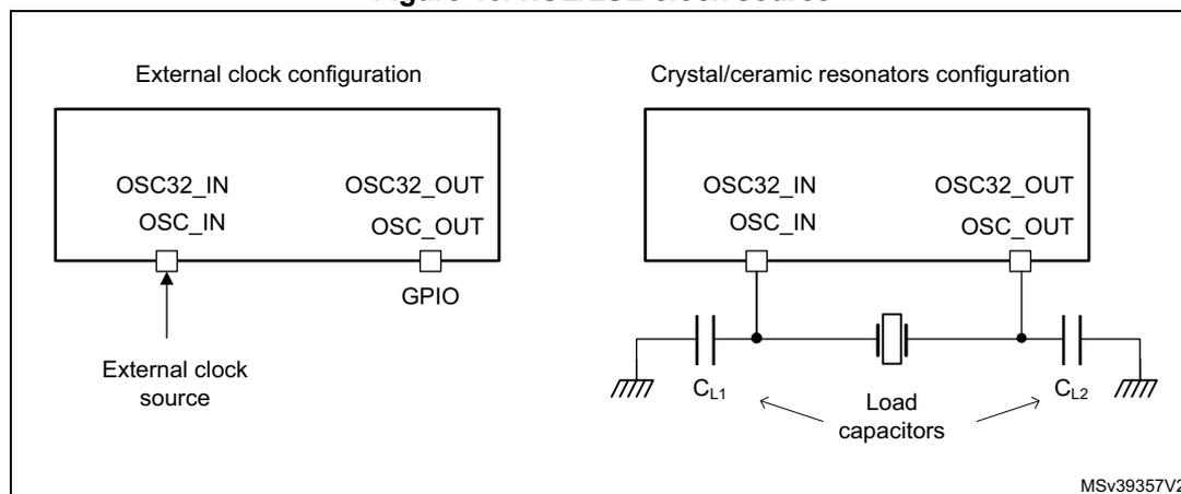
Figure 46. HSE/LSE clock source
External clock source (HSE bypass)
In this mode, an external clock source must be provided to OSC_IN pin. This mode is selected by setting the HSEBYP and HSEON bits of the RCC source control register (RCC_CR) to 1. The external clock source (square, sinus or triangle) with ~50% duty cycle has to drive the OSC_IN pin.
External crystal/ceramic resonator
The oscillator is enabled by setting the HSEBYP bit to 0 and HSEON bit to 1.
The HSE can be used when the product requires a very accurate high-speed clock.
The associated hardware configuration is shown in Figure 46 : the resonator and the load capacitors have to be placed as close as possible to the oscillator pins in order to minimize output distortion and startup stabilization time. The loading capacitance values must be adjusted according to the selected crystal or ceramic resonator. Refer to the electrical characteristics section of the datasheet for more details.
The HSERDY flag of the RCC source control register (RCC_CR) , indicates whether the HSE oscillator is stable or not. At startup, the hse_ck clock is not released until this bit is set by hardware. An interrupt can be generated if enabled in the RCC clock source interrupt enable register (RCC_CIER) .
The HSE can be switched ON and OFF through the HSEON bit. Note that the HSE cannot be switched OFF if one of the two conditions is met:
- • The HSE is used directly (via software mux) as system clock
- • The HSE is selected as reference clock for PLL1, with PLL1 enabled and selected to provide the system clock (via software mux).
In that case the hardware does not allow programming the HSEON bit to 0.
The HSE is automatically disabled by hardware, when the system enters Stop or Standby mode (refer to Section 8.5.7: Handling clock generators in Stop and Standby mode for additional information).
In addition, the HSE clock can be driven to the MCO1 and MCO2 outputs and used as clock source for other application components.
LSE oscillator
The LSE block can generate a clock from two possible sources:
- • External crystal/ceramic resonator
- • External user clock
External clock source (LSE bypass)
In this mode, an external clock source must be provided to OSC32_IN pin. The input clock can have a frequency up to 1 MHz. This mode is selected by setting the LSEBYP and LSEON bits of RCC backup domain control register (RCC_BDCR) to 1. The external clock signal (square, sinus or triangle) with ~50% duty cycle has to drive the OSC32_IN pin.
External crystal/ceramic resonator (LSE crystal)
The LSE clock is generated from a 32.768 kHz crystal or ceramic resonator. It has the advantage to provide a low-power highly accurate clock source to the real-time clock (RTC) for clock/calendar or other timing functions.
The LSERDY flag of the RCC backup domain control register (RCC_BDCR) indicates whether the LSE crystal is stable or not. At startup, the LSE crystal output clock signal is not released until this bit is set by hardware. An interrupt can be generated if enabled in the RCC clock source interrupt enable register (RCC_CIER) .
The LSE oscillator is switched ON and OFF using the LSEON bit. The LSE remains enabled when the system enters Stop or Standby mode.
In addition, the LSE clock can be driven to the MCO1 output and used as clock source for other application components.
The LSE also offers a programmable driving capability (LSEDRV[1:0]) that can be used to modulate the amplifier driving capability. This driving capability must be chosen according to the external crystal/ceramic component requirement to insure a stable oscillation. The driving capability must be set before enabling the LSE oscillator.
HSI oscillator
The HSI block provides the default clock to the product.
The HSI is a high-speed internal RC oscillator which can be used directly as system clock, peripheral clock, or as PLL input. A pres divider allows the application to select an HSI output frequency of 8, 16, 32 or 64 MHz. This pres divider is controlled by the HSIDIV.
The HSI advantages are the following:
- • Low-cost clock source since no external crystal is required
- • Faster startup time than HSE (a few microseconds)
The HSI frequency, even with frequency calibration, is less accurate than an external crystal oscillator or ceramic resonator.
The HSI can be switched ON and OFF using the HSION bit. Note that the HSI cannot be switched OFF if one of the two conditions is met:
- • The HSI is used directly (via software mux) as system clock
- • The HSI is selected as reference clock for PLL1, with PLL1 enabled and selected to provide the system clock (via software mux).
In that case the hardware does not allow programming the HSION bit to 0.
Note that the HSIDIV cannot be changed if the HSI is selected as reference clock for at least one enabled PLL (PLLxON bit set to 1). In that case the hardware does not update the HSIDIV with the new value. However it is possible to change the HSIDIV if the HSI is used directly as system clock.
The HSIRDY flag indicates if the HSI is stable or not. At startup, the HSI output clock is not released until this bit is set by hardware.
The HSI clock can also be used as a backup source (auxiliary clock) if the HSE fails (refer to Section : CSS on HSE ). The HSI can be disabled or not when the system enters Stop mode, please refer to Section 8.5.7: Handling clock generators in Stop and Standby mode for additional information.
In addition, the HSI clock can be driven to the MCO1 output and used as clock source for other application components.
Care must be taken when the HSI is used as kernel clock for communication peripherals, the application must take into account the following parameters:
- • the time interval between the moment where the peripheral generates a kernel clock request and the moment where the clock is really available,
- • the frequency accuracy.
Note: The HSI can remain enabled when the system is in Stop mode (see Section 8.5.7 for additional information).
HSION, HSIRDY and HSIDIV bits are located in the RCC source control register (RCC_CR) .
HSI calibration
RC oscillator frequencies can vary from one chip to another due to manufacturing process variations. That is why each device is factory calibrated by STMicroelectronics to improve accuracy (refer to the product datasheet for more information).
After a power-on reset, the factory calibration value is loaded in the HSICAL[11:0] bits.
If the application is subject to voltage or temperature variations, this may affect the RC oscillator frequency. The user application can trim the HSI frequency using the HSITRIM bits.
CSI oscillator
The CSI is a low-power RC oscillator which can be used directly as system clock, peripheral clock, or PLL input.
The CSI advantages are the following:
- • Low-cost clock source since no external crystal is required
- • Faster startup time than HSE (a few microseconds)
- • Very low-power consumption,
The CSI provides a clock frequency of about 4 MHz, while the HSI is able to provide a clock up to 64 MHz.
CSI frequency, even with frequency calibration, is less accurate than an external crystal oscillator or ceramic resonator.
The CSI can be switched ON and OFF through the CSION bit. The CSIRDY flag indicates whether the CSI is stable or not. At startup, the CSI output clock is not released until this bit is set by hardware.
The CSI cannot be switched OFF if one of the two conditions is met:
- • The CSI is used directly (via software mux) as system clock
- • The CSI is selected as reference clock for PLL1, with PLL1 enabled and selected to provide the system clock (via software mux).
In that case the hardware does not allow programming the CSION bit to 0.
The CSI can be disabled or not when the system enters Stop mode (refer to Section 8.5.7: Handling clock generators in Stop and Standby mode for additional information).
In addition, the CSI clock can be driven to the MCO2 output and used as clock source for other application components.
Even if the CSI settling time is faster than the HSI, care must be taken when the CSI is used as kernel clock for communication peripherals: the application has to take into account the following parameters:
- • the time interval between the moment where the peripheral generates a kernel clock request and the moment where the clock is really available,
- • the frequency precision.
CSI calibration
RC oscillator frequencies can vary from one chip to another due to manufacturing process variations, this is why each device is factory calibrated by STMicroelectronics to achieve improved accuracy (refer to the product datasheet for more information).
After reset, the factory calibration value is loaded in the CSICAL[7:0] bits.
If the application is subject to voltage or temperature variations, this may affect the RC oscillator frequency. The user application can trim the CSI frequency using the CSITRIM bits.
HSI48 oscillator
The HSI48 is an RC oscillator that delivers a 48 MHz clock that can be used directly as kernel clock for some peripherals.
The HSI48 oscillator mainly aims at providing a high precision clock to the USB peripheral by means of a special Clock Recovery System (CRS) circuitry, which could use the USB SOF signal, the LSE, or an external signal, to automatically adjust the oscillator frequency on-the-fly, in very small granularity.
The HSI48 oscillator is disabled as soon as the system enters Stop or Standby mode. When the CRS is not used, this oscillator is free running and thus subject to manufacturing process variations. That is why each device is factory calibrated by STMicroelectronics to achieve an accuracy of ACC HSI48 (refer to the product datasheet for more information).
For more details on how to configure and use the CRS, please refer to Section 9: Clock recovery system (CRS) .
The HSI48RDY flag indicates whether the HSI48 oscillator is stable or not. At startup, the HSI48 output clock is not released until this bit is set by hardware.
The HSI48 can be switched ON and OFF using the HSI48ON bit.
The HSI48 clock can also be driven to the MCO1 multiplexer and used as clock source for other application components.
Note: HSI48ON and HSI48RDY bits are located in the RCC source control register (RCC_CR) .
LSI oscillator
The LSI acts as a low-power clock source that can be kept running when the system is in Stop or Standby mode for the independent watchdog (IWDG) and Auto-Wakeup Unit (AWU). The clock frequency is around 32 kHz. For more details, refer to the electrical characteristics section of the datasheet.
The LSI can be switched ON and OFF using the LSION bit. The LSIRDY flag indicates whether the LSI oscillator is stable or not. If an independent watchdog is started either by hardware or software, the LSI is forced ON and cannot be disabled.
The LSI remains enabled when the system enters Stop or Standby mode (refer to Section 8.5.7: Handling clock generators in Stop and Standby mode for additional information).
At LSI startup, the clock is not provided until the hardware sets the LSIRDY bit. An interrupt can be generated if enabled in the RCC clock source interrupt enable register (RCC_CIER) .
In addition, the LSI clock can be driven to the MCO2 output and used as a clock source for other application components.
Note: Bits LSION and LSIRDY are located into the RCC Clock Control and Status Register (RCC_CSR) .
8.5.3 Clock Security System (CSS)
CSS on HSE
The clock security system can be enabled by software via the HSECSSON bit. The HSECSSON bit can be enabled even when the HSEON is set to 0.
The CSS on HSE is enabled by the hardware when the HSE is enabled and ready, and HSECSSON set to 1.
The CSS on HSE is disabled when the HSE is disabled. As a result, this function does not work when the system is in Stop mode.
It is not possible to clear directly the HSECSSON bit by software.
The HSECSSON bit is cleared by hardware when a system reset occurs or when the system enters Standby mode (see Section 8.4.2: System reset ).
If a failure is detected on the HSE clock, the system automatically switches to the HSI in order to provide a safe clock. The HSE is then automatically disabled, a clock failure event is sent to the break inputs of advanced-control timers (TIM1, TIM8, TIM15, TIM16, and TIM17), and an interrupt is generated to inform the software about the failure (CSS interrupt: rcc_hsecss_it ), thus allowing the MCU to perform rescue operations. If the HSE output was used as clock source for PLLs when the failure occurred, the PLLs are also disabled.
If an HSE clock failure occurs when the CSS is enabled, the CSS generates an interrupt which causes the automatic generation of an NMI. The HSECSSF flag in RCC clock source interrupt flag register (RCC_CIFR) is set to 1 to allow the application to identify the failure source. The NMI routine is executed indefinitely until the HSECSSF bit is cleared. As a consequence, the application has to clear the HSECSSF flag in the NMI ISR by setting the HSECSSC bit in the RCC clock source interrupt clear register (RCC_CICR) .
CSS on LSE
A clock security system on the LSE oscillator can be enabled by software by programming the LSECSSON bit in the RCC backup domain control register (RCC_BDCR) .
This bit can be disabled only by hardware when the following conditions are met:
- • after a pwr_vsw_rst ( \( V_{SW} \) software reset)
- • or after a failure detection on LSE.
LSECSSON bit must be written after the LSE is enabled (LSEON bit set by software) and ready (LSERDY set by hardware), and after the RTC clock has been selected through the RTCSEL bit.
The CSS on LSE works in all modes (Run, Stop and Standby) except VBAT.
If an LSE failure is detected, the LSE clock is no more delivered to the RTC but the value of RTCSEL, LSECSSON and LSEON bits are not changed by the hardware.
A wakeup is generated in Standby mode. In other modes an interrupt ( rcc_lsecss_it ) can be sent to wake up the software. The software must then disable the LSECSSON bit, stop the defective LSE (clear LSEON bit), and can change the RTC clock source (no clock or LSI or HSE) through RTCSEL bits, or take any required action to secure the application.
8.5.4 Clock output generation (MCO1/MCO2)
Two micro-controller clock output (MCO) pins, MCO1 and MCO2, are available. A clock source can be selected for each output. The selected clock can be divided thanks to configurable prescaler (refer to Figure 45 for additional information on signal selection).
MCO1 and MCO2 outputs are controlled via MCO1PRE[3:0], MCO1[2:0], MCO2PRE[3:0] and MCO2[2:0] located in the RCC clock configuration register (RCC_CFGR) .
The GPIO port corresponding to each MCO pin, has to be programmed in alternate function mode.
The clock provided to the MCOs outputs must not exceed the maximum pin speed (refer to the product datasheet for information on the supported pin speed).
8.5.5 PLL description
The RCC features three PLLs:
- • A main PLL, PLL1, which is generally used to provide clocks to the CPU and to some peripherals.
- • Two dedicated PLLs, PLL2 and PLL3, which are used to generate the kernel clock for peripherals.
The PLLs integrated into the RCC are completely independent. They offer the following features:
- • Two embedded VCOs:
- – A wide-range VCO (VCOH)
- – A low-frequency VCO (VCOL)
- • Input frequency range:
- – 1 to 2 MHz when VCOL is used
- – 2 to 16 MHz when VCOH is used
- • Capability to work either in integer or Fractional mode
- • 13-bit Sigma-Delta modulator, allowing to fine-tune the VCO frequency by steps of 11 to 0.3 ppm.
- • The Sigma-Delta modulator can be updated on-the-fly, without generating frequency overshoots on PLLs outputs.
- • Each PLL offer 3 outputs with post-dividers
Figure 47. PLL block diagram
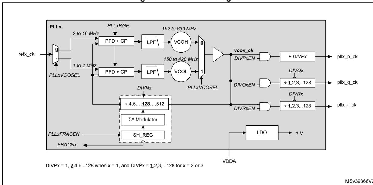
DIVPx = 1, 2, 4, 6...128 when x = 1, and DIVPx = 1, 2, 3...128 for x = 2 or 3
MSV39366V2
The PLLs are controlled via
RCC_PLLxDIVR
,
RCC_PLLxFRACR
,
RCC_PLLCFGR
and
RCC_CR
registers.
The frequency of the reference clock provided to the PLLs (
refx_ck
) must range from 1 to 16 MHz. The user application has to program properly the
DIVMx
dividers of the
RCC PLLs clock source selection register (RCC_PLLCKSELR)
in order to match this condition. In addition, the
PLLxRGE
of the
RCC PLLs Configuration Register (RCC_PLLCFGR)
field must be set according to the reference input frequency to guarantee an optimal performance of the PLL.
The user application can then configure the proper VCO: if the frequency of the reference clock is lower or equal to 2 MHz, then
VCOL
must be selected. Otherwise for a frequency equal or higher to 2 MHz,
VCOH
must be chosen. To reduce the power consumption, it is recommended to configure the VCO output to the lowest frequency.
DIVNx
loop divider has to be programmed to achieve the expected frequency at VCO output. In addition, the VCO output range must be respected.
The PLLs operate in integer mode when the value of
SH_REG
(
FRACNx
shadow register) is set to 0. The
SH_REG
is updated with the
FRACNx
value when
PLLxFRACEN
bit goes from 0 to 1. The Sigma-Delta modulator is designed in order to minimize the jitter impact while allowing very small frequency steps.
The PLLs can be enabled by setting
PLLxON
to 1. The bits
PLLxRDY
indicate that the PLL is ready (i.e. locked).
Note:
Before enabling the PLLs, make sure that the reference frequency (
refx_ck
) provided to the PLL is stable, so the hardware does not allow changing
DIVMx
when the
PLLx
is ON and it is also not possible to change
PLLSRC
when one of the PLL is ON.
The hardware prevents writing
PLL1ON
to 0 if the
PLL1
is currently used to deliver the system clock. There are other hardware protections on the clock generators (refer to sections
HSE oscillator
,
HSI oscillator
and
CSI oscillator
).
The following PLL parameters cannot be changed once the PLL is enabled: DIVNx, PLLxRGE, PLLxVCOSEL, DIVPx, DIVQx, DIVRx, DIVPxEN, DIVQxEN and DIVRxEN.
To insure an optimal behavior of the PLL when one of the post-divider (DIVP, DIVQ or DIVR) is not used, the application shall set the enable bit (DIVyEN) as well as the corresponding post-divider bits (DIVP, DIVQ or DIVR) to 0.
If the above rules are not respected, the PLL output frequency is not guaranteed.
Output frequency computation
When the PLL is configured in integer mode (SH_REG = 0), the VCO frequency ( \( F_{VCO} \) ) is given by the following expression:
When the PLL is configured in fractional mode (SH_REG different from 0), the DIVN divider must be initialized before enabling the PLLs. However, it is possible to change the value of FRACNx on-the-fly without disturbing the PLL output.
This feature can be used either to generate a specific frequency from any crystal value with a good accuracy, or to fine-tune the frequency on-the-fly.
For each PLL, the VCO frequency is given by the following formula:
Note: For PLL1, DIVP bitfield can only take odd values or 1 (no division).
The PLLs are disabled by hardware when:
- • The system enters Stop or Standby mode.
- • An HSE failure occurs when HSE or PLL (clocked by HSE) are used as system clock.
PLL initialization phase
Figure 48 shows the recommended PLL initialization sequence in integer and fractional mode. The PLLx are supposed to be disabled at the start of the initialization sequence:
- 1. Initialize the PLLs registers according to the required frequency.
- – Set PLLxFRACEN of RCC PLLs Configuration Register (RCC_PLLCFGR) to 0 for integer mode.
- – For fractional mode, set FRACN to the required initial value (FracInitValue) and then set PLLxFRACEN to 1.
- 2. Once the PLLxON bit is set to 1, the user application has to wait until PLLxRDY bit is set to 1. If the PLLx is in fractional mode, the PLLxFRACEN bit must not be set back to 0 as long as PLLxRDY = 0.
- 3. Once the PLLxRDY bit is set to 1, the PLLx is ready to be used.
- 4. If the application intends to tune the PLLx frequency on-the-fly (possible only in fractional mode), then:
- a) PLLxFRACEN must be set to 0,
When PLLxFRACEN = 0, the Sigma-Delta modulator is still operating with the value latched into SH_REG. - b) A new value must be uploaded into PLLxFRACR (FracValue(n)).
- c) PLLxFRACEN must be set to 1, in order to latch the content of PLLxFRACR into its shadow register.
- a) PLLxFRACEN must be set to 0,
Note: When the PLLxRDY goes to 1, it means that the difference between the PLLx output frequency and the target value is lower than \( \pm 2\% \) .
Figure 48. PLLs Initialization Flowchart
graph TD
    subgraph IntegerMode [ ]
        direction TB
        I1([PLL enable sequence integer mode]) --> I2[Select clock source (RCC_CKSELR)
- (PLL SRC)]
        I2 --> I3[Init pre-divider (RCC_CKSELR)
- DIVMx]
        I3 --> I4[PLLx config (RCC_PLLCFGR)
- PLLxVCOSEL, PLLxRGE
- PLLxFRACEN = 0
- DIVPxEN, DIVQxEN, DIVRxEN
Init PLLx dividers (RCC_PLLxDIVR)
- DIVNx, DIVPx, DIVQx, DIVRx]
        I4 --> I5[Enable PLLx (RCC_CR)
- PLLxON = 1]
        I5 --> I6{PLLxRDY = 1 ?}
        I6 -- No --> I5
        I6 -- Yes --> I7([Ready for use in integer mode])
    end

    subgraph FractionalMode [ ]
        direction TB
        F1([PLL enable sequence fractional mode]) --> F2[Select clock source (RCC_CKSELR)
- (PLL SRC)]
        F2 --> F3[Init pre-divider (RCC_CKSELR)
- DIVMx]
        F3 --> F4[Init fractional value (RCC_PLLxFRACR)
- FRACN= FracInitValue
PLLx config (RCC_PLLCFGR)
- PLLxVCOSEL, PLLxRGE
- PLLxFRACEN = 1
- DIVPxEN, DIVQxEN, DIVRxEN
Init PLLx dividers (RCC_PLLxDIVR)
- DIVNx, DIVPx, DIVQx, DIVRx]
        F4 --> F5[Enable PLLx (RCC_CR)
- PLLxON = 1]
        F5 --> F6{PLLxRDY = 1 ?}
        F6 -- No --> F5
        F6 -- Yes --> F7([Ready for use in fractional mode])
    end

    I3 -.-> F3
    F3 -.-> I3
    F3 -.-> F3R[Can be repeated for each PLL]

    I7 --> F8[Disable fractional mode (RCC_PLLCFGR)
- PLLxFRACEN = 0
Init fractional value (RCC_PLLxFRACR)
- FRACN= FracValue(n)
Enable fractional mode (RCC_PLLCFGR)
- PLLxFRACEN = 1]
    F8 --> F9([Ready for use in fractional mode])
    F8 -.-> F8R[Value update on-the-fly]
    F9 -.-> F8R
    F8R -.-> F9
MSV39367V1
8.5.6 System clock (sys_ck)
System clock selection
After a system reset, the HSI is selected as system clock and all PLLs are switched OFF. When a clock source is used for the system clock, it is not possible for the software to disable the selected source via the xxxON bits.
Of course, the system clock can be stopped by the hardware when the System enters Stop or Standby mode.
When the system is running, the user application can select the system clock ( sys_ck ) among the 4 following sources:
- • HSE
- • HSI
- • CSI or
- • pll1_p_ck
This function is controlled by programming the RCC clock configuration register (RCC_CFGR) . A switch from one clock source to another occurs only if the target clock source is ready (clock stable after startup delay or PLL locked). If a clock source that is not yet ready is selected, the switch occurs when the clock source is ready.
The SWS status bits in the RCC clock configuration register (RCC_CFGR) indicate which clock is currently used as system clock. The other status bits in the RCC_CR register indicate which clock(s) is (are) ready.
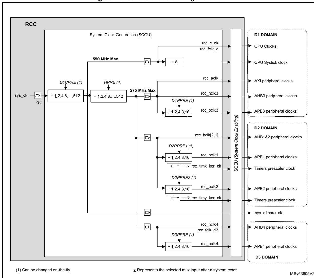
System clock generation
Figure 49 shows a simplified view of the clock distribution for the CPU and busses. All the dividers shown in the block diagram can be changed on-the-fly without generating timing violations. This feature is a very simply solution to adapt the busses frequencies to the application needs, thus optimizing the power consumption.
The D1CPRE divider can be used to adjust the CPU clock. However this also impacts the clock frequency of all bus matrix.
In the same way, HPRE divider can be used to adjust the clock for D1 domain bus matrix, but this also impacts the clock frequency of bus matrix of D2 and D3 domains.
Most of the prescalers are controlled via RCC_D1CFGR, RCC_D2CFGR and RCC_D3CFGR registers.
Figure 49. Core and bus clock generation
(1) Can be changed on-the-fly
x Represents the selected mux input after a system reset
MSV63805V2
This block also provides the clock for the timers ( rcc_timx_ker_ck and rcc_timy_ker_ck ). The frequency of the timers clock depends on the APB prescaler corresponding to the bus to which the timer is connected, and on TIMPRE bit. Table 53 shows how to select the timer clock frequency.
Table 53. Ratio between clock timer and pclk
| D2PPRE1 (1) D2PPRE2 | TIMPRE (2) | F
rcc_timx_ker_ck F rcc_timy_ker_ck | F
rcc_pclk1 F rcc_pclk2 | Comments | |
|---|---|---|---|---|---|
| 0xx | 0 | → | F rcc_hclk1 | F rcc_hclk1 | The timer clock is equal to the bus clock. |
| 100 | 0 | → | F rcc_hclk1 | F rcc_hclk1 / 2 | The timer clock is twice as fast as the bus clock. |
| 101 | 0 | → | F rcc_hclk1 / 2 | F rcc_hclk1 / 4 | |
| 110 | 0 | → | F rcc_hclk1 / 4 | F rcc_hclk1 / 8 | |
| 111 | 0 | → | F rcc_hclk1 / 8 | F rcc_hclk1 / 16 |
Table 53. Ratio between clock timer and pclk (continued)
| D2PPRE1 (1) D2PPRE2 | TIMPRE (2) | \(
F_{rcc\_timx\_ker\_ck}
\) \( F_{rcc\_timy\_ker\_ck} \) | \(
F_{rcc\_pclk1}
\) \( F_{rcc\_pclk2} \) | Comments | |
|---|---|---|---|---|---|
| 0xx | 1 | → | \( F_{rcc\_hclk1} \) | \( F_{rcc\_hclk1} \) | The timer clock is equal to the bus clock. |
| 100 | 1 | → | \( F_{rcc\_hclk1} \) | \( F_{rcc\_hclk1} / 2 \) | The timer clock is twice as fast as the bus clock. |
| 101 | 1 | → | \( F_{rcc\_hclk1} \) | \( F_{rcc\_hclk1} / 4 \) | The timer clock is 4 times faster than the bus clock. |
| 110 | 1 | → | \( F_{rcc\_hclk1} / 2 \) | \( F_{rcc\_hclk1} / 8 \) | |
| 111 | 1 | → | \( F_{rcc\_hclk1} / 4 \) | \( F_{rcc\_hclk1} / 16 \) |
1. D2PPRE1 and D2PPRE2 belong to RCC domain 2 clock configuration register (RCC_D2CFGR) .
2. TIMPRE belongs to RCC clock configuration register (RCC_CFGR) .
8.5.7 Handling clock generators in Stop and Standby mode
When the whole system enters Stop mode, all the clocks (system and kernel clocks) are stopped as well as the following clock sources:
- • CSI, HSI (depending on HSIKERON, and CSIKERON bits)
- • HSE
- • PLL1, PLL2 and PLL3
- • HSI48
The content of the RCC registers is not altered except for PLL1ON, PLL2ON, PLL3ON HSEON and HSI48ON which are set to 0.
Exiting Stop mode
When the microcontroller exits system Stop mode via a wake-up event, the application can select which oscillator (HSI and/or CSI) will be used to restart. The STOPWUCK bit selects the oscillator used as system clock. The STOPKERWUCK bit selects the oscillator used as kernel clock for peripherals. The STOPKERWUCK bit is useful if after a system Stop a peripheral needs a kernel clock generated by an oscillator different from the one used for the system clock.
All these bits belong to the RCC clock configuration register (RCC_CFGR) . Table 54 gives a detailed description of their behavior.
Table 54. STOPWUCK and STOPKERWUCK description
| STOPWUCK | STOPKERWUCK | Activated oscillator when the system exits Stop mode | Distributed clocks when System exits Stop mode | ||
|---|---|---|---|---|---|
| System Clock | Kernel Clock | ||||
| 0 | 0 | → | HSI | HSI | HSI |
| 1 | → | HSI and CSI | HSI and/or CSI | ||
| 1 | 0 | → | HSI and CSI | CSI | HSI and/or CSI |
| 1 | → | CSI | CSI | ||
During Stop mode
There are two specific cases where the HSI or CSI can be enabled during system Stop mode:
- • When a dedicated peripheral requests the kernel clock:
In this case the peripheral will receive the HSI or CSI according to the kernel clock source selected for this peripheral (via PERxSRC). - • When the bits HSIKERON or CSIKERON are set:
In this case the HSI and CSI are kept running during Stop mode but the outputs are gated. In that way, the clock will be available immediately when the system exits Stop mode or when a peripheral requests the kernel clock (see Table 55 for details).
HSIKERON and CSIKERON bits belong to RCC source control register (RCC_CR) . Table 55 gives a detailed description of their behavior.
Table 55. HSIKERON and CSIKERON behavior
| HSIKERON (CSIKERON) | HSI (CSI) state during Stop mode | HSI (CSI) Setting time | |
|---|---|---|---|
| 0 | → | OFF | \( t_{su(HSI)} (t_{su(CSI)})^{(1)} \) |
| 1 | → | Running and Gated | Immediate |
- 1. \( t_{su(HSI)} \) and \( t_{su(CSI)} \) are the startup times of the HSI and CSI oscillators (see refer to the product datasheet for the values of these parameters).
When the microcontroller exists system Standby mode, the HSI is selected as system and kernel clock, the RCC registers are reset to their initial values except for the RCC_RSR (or RCC_C1_RSR) and RCC_BDCR registers.
Note as well that the HSI and CSI outputs provide two clock paths (see Figure 45 ):
- • one path for the system clock ( hsi_ck or csi_ck )
- • one path for the peripheral kernel clock ( hsi_ker_ck or csi_ker_ck ).
When a peripheral requests the kernel clock in system Stop mode, only the path providing the hsi_ker_ck or csi_ker_ck is activated.
Caution: It is not guaranteed that the CPU will get automatically the same clock frequencies when leaving CStop mode: this mainly depends on the System state. For example If the CPU goes to CStop, while the D3 domain is kept in CRun, when the CPU exits from CStop, the clock settings remain unchanged. If the D3 domain goes to CStop while the CPU is also in CStop, then when the CPU exits from CStop, the CPU will operate with HSI or CSI when it left the CStop mode.
8.5.8 Kernel clock selection
Some peripherals are designed to work with two different clock domains that operate asynchronously:
- • a clock domain synchronous with the register and bus interface ( ckg_bus_perx clock)
- • and a clock domain generally synchronous with the peripheral (kernel clock).
The benefit of having peripherals supporting these two clock domains is that the user application has more freedom to choose optimized clock frequency for the CPU, bus matrix and for the kernel part of the peripheral.
As a consequence, the user application can change the bus frequency without reprogramming the peripherals. As an example an on-going transfer with UART will not be disturbed if its APB clock is changed on-the-fly.
Table 56 shows the kernel clock that the RCC can deliver to the peripherals. Each row of Table 56 represents a MUX and the peripherals connected to its output. The columns starting from number 5 represents the clock sources. Column 3 gives the maximum allowed frequency at each MUX output. It is up to the user to respect these requirements.
Table 56. Kernel clock distribution overview
| Peripherals | Clock mux control bits | Maximum allowed frequency [MHz] | Domain | Clock sources | ||||||||||||||||||||||
|---|---|---|---|---|---|---|---|---|---|---|---|---|---|---|---|---|---|---|---|---|---|---|---|---|---|---|
| VOS0 | VOS1 | VOS2 | VOS3 | pll1_q_ck | pll2_p_ck | pll2_q_ck | pll2_r_ck | pll3_p_ck | pll3_q_ck | pll3_r_ck | sys_ck | bus clocks (1) | hse_ck | hsi_ker_ck | csi_ker_ck | hsi48_ck | lse_ck | lsi_ck | per_ck (2) | I2S_CKIN | USB_PHY1 | spdifrx_symb_ck | Disabled | |||
| LTDC | - | 166 | 100 | 75 | 50 | D1 | x | |||||||||||||||||||
| FMC | FMCSEL | 275 | 200 | 150 | 100 | 1 | 2 | 0 | 3 | |||||||||||||||||
| OCTOSPI | OCTOSPISEL | 333 | 200 | 150 | 100 | 1 | 2 | 0 | 3 | |||||||||||||||||
| SDMMC1 | SDMMCSEL | 250 (4) | 200 (4) | 150 (4) | 100 (4) | 0 | 1 | |||||||||||||||||||
| SDMMC2 | 250 | 200 | 150 | 100 | ||||||||||||||||||||||
| DFSDM1 Aclk | SAI1SEL | 250 | 200 | 150 | 100 | D2 | 0 | 1 | 2 | 4 | 3 | |||||||||||||||
| DFSDM1 clk | DFSDM1SEL | 275 | 200 | 150 | 85 | 1 | 0 | |||||||||||||||||||
| FDCAN | FDCANSEL | 125 | 100 | 75 | 50 | 1 | 2 | 0 | ||||||||||||||||||
| HDMI-CEC | CECSEL | 1 | 1 | 1 | 1 | 2 (3) | 0 | 1 | ||||||||||||||||||
| I2C1,2,3, 5 | I2C1235SEL | 137.5 | 100 | 75 | 43 | 1 | 0 | 2 | 3 | |||||||||||||||||
| LPTIM1 | LPTIM1SEL | 137.5 | 100 | 75 | 43 | 1 | 2 | 0 | 3 | 4 | 5 | |||||||||||||||
| TIM[8:1][17:12] | - | 275 | 200 | 150 | 85 | x | ||||||||||||||||||||
| RNG | RNGSEL | 250 | 200 | 150 | 100 | 1 | 0 | 2 | 3 | |||||||||||||||||
| SAI1 | SAI1SEL | 166 | 150 | 113 | 75 | 0 | 1 | 2 | 4 | 3 | ||||||||||||||||
| SPDIFRX | SPDIFRXSEL | 250 | 200 | 150 | 100 | 0 | 1 | 2 | 3 | |||||||||||||||||
| SPI(I2S)1,2,3 | SPI123SEL | 250 | 180 | 125 | 75 | 0 | 1 | 2 | 4 | 3 | ||||||||||||||||
Table 56. Kernel clock distribution overview (continued)
| Peripherals | Clock mux control bits | Maximum allowed frequency [MHz] | Domain | Clock sources | |||||||||||||||||||||||
|---|---|---|---|---|---|---|---|---|---|---|---|---|---|---|---|---|---|---|---|---|---|---|---|---|---|---|---|
| VOS0 | VOS1 | VOS2 | VOS3 | pll1_q_ck | pll2_p_ck | pll2_q_ck | pll2_r_ck | pll3_p_ck | pll3_q_ck | pll3_r_ck | sys_ck | bus clocks (1) | hse_ck | hsi_ker_ck | csi_ker_ck | hsi48_ck | lse_ck | lsi_ck | per_ck (2) | I2S_CKIN | USB_PHY1 | spdifrx_symb_ck | Disabled | ||||
| SPI4,5 | SPI45SEL | 250 | 180 | 125 | 75 | D2 | 1 | 2 | 0 | 5 | 3 | 4 | |||||||||||||||
| SWPMI | SWPMISEL | 137.5 | 100 | 75 | 43 | 0 | 1 | ||||||||||||||||||||
| USART1,6, 10 UART9 | USART16910SEL | 137.5 | 100 | 75 | 43 | 1 | 2 | 0 | 3 | 4 | 5 | ||||||||||||||||
| USART2,3 UART4,5,7,8 | USART234578SEL | 137.5 | 100 | 75 | 43 | 1 | 2 | 0 | 3 | 4 | 5 | ||||||||||||||||
| USB1OTG | USBSEL | 125 | 100 | 50 | 50 | 1 | 2 | 3 | 0 | ||||||||||||||||||
| USB1ULPI | - | 60 | 60 | 45 | 40 | x | |||||||||||||||||||||
| ADC1,2, 3 | ADCSEL | 160 (4) | 160 (4) | 60 | 40 (4) | 0 | 1 | 2 | |||||||||||||||||||
| I2C4 | I2C4SEL | 137.5 | 100 | 75 | 43 | D3 | 1 | 0 | 2 | 3 | |||||||||||||||||
| LPTIM2 | LPTIM2SEL | 137.5 | 100 | 75 | 43 | 1 | 2 | 0 | 3 | 4 | 5 | ||||||||||||||||
| LPTIM3,4,5 | LPTIM345SEL | 137.5 | 100 | 75 | 43 | 1 | 2 | 0 | 3 | 4 | 5 | ||||||||||||||||
| LPUART1 | LPUART1SEL | 137.5 | 100 | 75 | 43 | 1 | 2 | 0 | 3 | 4 | 5 | ||||||||||||||||
| SAI4_A | SAI4ASEL | 166 | 150 | 113 | 75 | 0 | 1 | 2 | 4 | 3 | 5 | ||||||||||||||||
| SAI4_B | SAI4BSEL | 166 | 150 | 113 | 75 | 0 | 1 | 2 | 4 | 3 | 5 | ||||||||||||||||
| SPI(I2S)6 | SPI6SEL | 250 | 180 | 125 | 75 | 1 | 2 | 0 | 5 | 3 | 4 | 6 | |||||||||||||||
| RTC/AWU | RTCSEL | 1 | VSW | 3 (5) | 1 | 2 | 0 | ||||||||||||||||||||
1. The bus clocks are the bus interface clocks to which the peripherals are connected, it can be APB, AHB or AXI clocks.
2. The per_ck clock could be hse_ck, hsi_ker_ck or csi_ker_ck according to CKPERSEL selection.
3. Clock CSI divided by 122.
4. With a duty cycle close to 50%, meaning that DIV[P/Q/R]x values shall be even. For SDMMCx, the duty cycle shall be 50% when supporting DDR.
5. Clock HSE divided by RTCPRE.
Figure 50 to Figure 60 provide a more detailed description of kernel clock distribution. To simplify the drawings, the bus interface clocks (pclk, hclk) are not represented, even if they are gated with enable signals. Refer to Section 8.5.11: Peripheral clock gating control for more details.
To reduce the amount of switches, some peripherals share the same kernel clock source. Nevertheless, all peripherals have their dedicated enable signal.
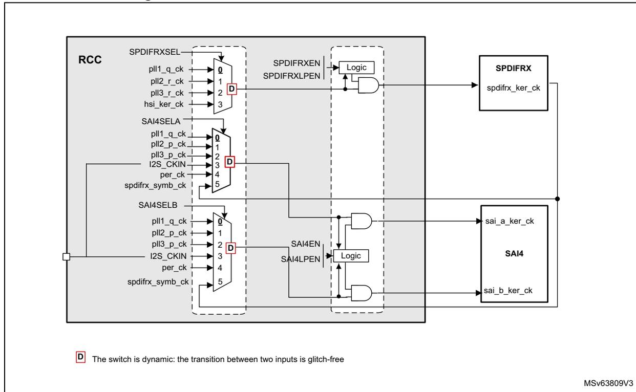
Peripherals dedicated to audio applications
The audio peripherals generally need specific accurate frequencies, except for SPDIFRX. As shown in Figure 50 and Figure 51 , the kernel clock of the SAIs or SPI(I2S)s can be generated by:
- • The PLL1 when the amount of active PLLs has to be reduced
- • The PLL2 or 3 for optimal flexibility in frequency generation
- • HSE, HSI or CSI for use-cases where the current consumption is critical
- • I2S_CKIN when an external clock reference need to be used.
Note: The SPDIFRX does not require a specific frequency, but only a kernel clock frequency high enough to make the peripheral work properly. Refer to the SPDIFRX description for more details.
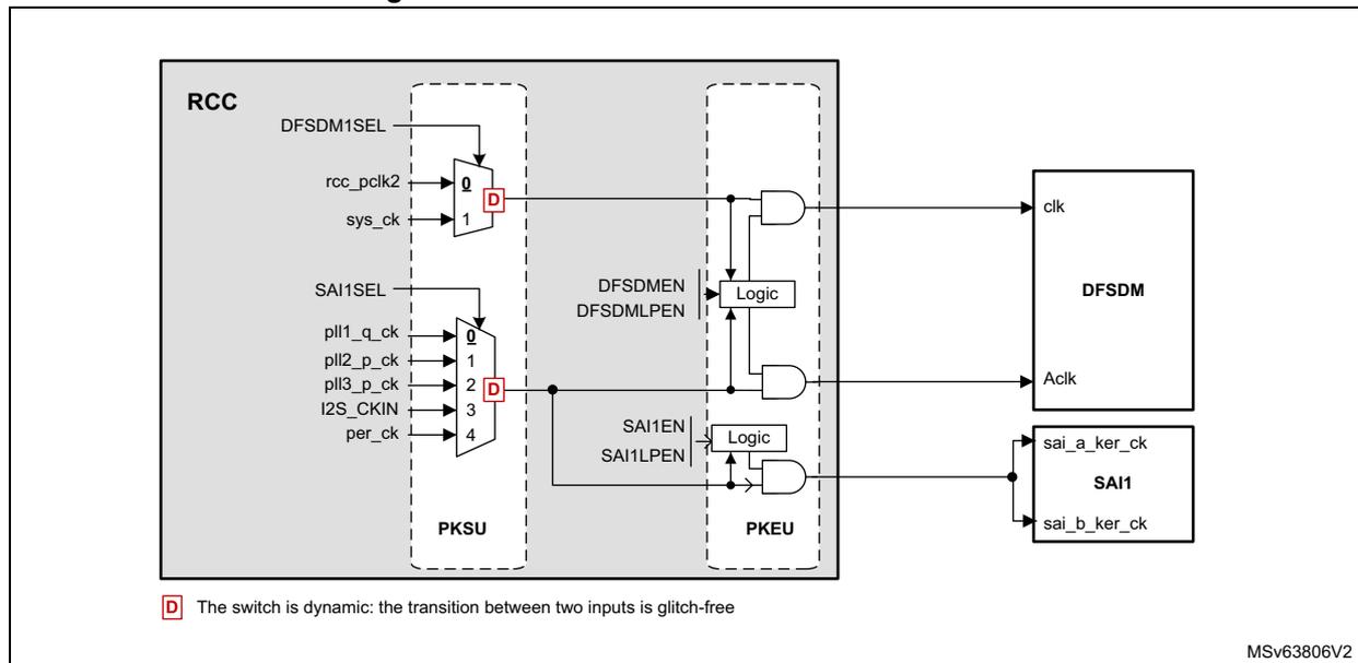
DFSDM1 can use the same clock as SAI1A. This is useful when DFSDM1 is used for audio applications.
To improve the flexibility, SAI4 can use different clock for each sub-block.
The SPI/I2S1, 2, and 3 share the same kernel clock source (see Figure 52 ).
Figure 50. Kernel clock distribution for SAIs and SPDIFRX
RCC
SPDIFRXSEL
- pll1_q_ck
- pll2_r_ck
- pll3_r_ck
- hsi_ker_ck
SAI4SEL A
- pll1_q_ck
- pll2_p_ck
- pll3_p_ck
- I2S_CKIN
- per_ck
- spdifrx_symb_ck
SAI4SEL B
- pll1_q_ck
- pll2_p_ck
- pll3_p_ck
- I2S_CKIN
- per_ck
- spdifrx_symb_ck
SPDIFRXEN
SPDIFRXLPEN
Logic
SPDIFRX
spdifrx_ker_ck
SAI4EN
SAI4LPEN
Logic
SAI4
sai_a_ker_ck
sai_b_ker_ck
D The switch is dynamic: the transition between two inputs is glitch-free
MSv63809V3
- 1. X represents the selected MUX input after a system reset.
- 2. This figure does not show the connection of the bus interface clock to the peripherals. For details on each enable cell, please refer to Section 8.5.11: Peripheral clock gating control .
Figure 51. Kernel clock distribution for DFSDM
RCC
DFSDM1SEL
- rcc_pclk2
- sys_ck
SAI1SEL
- pll1_q_ck
- pll2_p_ck
- pll3_p_ck
- I2S_CKIN
- per_ck
DFSDMEN
DFSDMLPEN
Logic
DFSDM
clk
Aclk
SAI1EN
SAI1LPEN
Logic
SAI1
sai_a_ker_ck
sai_b_ker_ck
D The switch is dynamic: the transition between two inputs is glitch-free
MSv63806V2
- 1. X represents the selected MUX input after a system reset.
- 2. This figure does not show the connection of the bus interface clock to the peripherals. For details on each enable cell, please refer to Section 8.5.11: Peripheral clock gating control .
Peripherals dedicated to control and data transfer
Peripherals such as SPIs, I2Cs, UARTs do not need a specific kernel clock frequency but a clock fast enough to generate the correct baud rate, or the required bit clock on the serial interface. For that purpose the source can be selected among:
- • PLL1 when the amount of active PLLs has to be reduced
- • PLL2 or PLL3 if better flexibility is required. As an example, this solution allows changing the frequency bus via PLL1 without affecting the speed of some serial interfaces.
- • HSI or CSI for low-power use-cases or when the peripheral has to quickly wake up from Stop mode (i.e. UART, I2C...).
Note: UARTs also need the LSE clock when high baud rates are not required.
Figure 52. Kernel clock distribution for SPIs and SPI/I2S
![Figure 52: Kernel clock distribution for SPIs and SPI/I2S. The diagram shows four clock multiplexers (MUX) within the RCC block, each selecting a clock source for a specific peripheral. The MUXes are labeled SPDIFRXSEL, SPI123SEL, SPI45SEL, and SPI6SEL. Each MUX has multiple inputs (PLL1, PLL2, PLL3, HSI, CSI, HSE, I2S_CKIN, etc.) and a dynamic switch (D) that selects one input. The selected clock is then passed through a Logic block (AND gate) along with an enable signal (e.g., SPDIFRXEN, SPI[3:1]EN, SPI[5:4]EN, SPI6AMEN) to the corresponding peripheral block: SPDIF-RX, SPI/I2S[3:1], SPI[5:4], and SPI/I2S6. The diagram also includes labels for PKSU and PKEU blocks. A legend at the bottom left indicates that 'D' represents a dynamic switch that is glitch-free.](/RM0468-STM32H723-733-725-735-730/715256755931ae8be93341625aefb19e_img.jpg)
D The switch is dynamic: the transition between two inputs is glitch-free
MSV63807V5
- 1. X represents the selected MUX input after a system reset.
- 2. This figure does not show the connection of the bus interface clock to the peripheral. or details on each enable cell, please refer to Section 8.5.11: Peripheral clock gating control .
Figure 53. Kernel clock distribution for I2Cs
![Schematic diagram of kernel clock distribution for I2Cs. It shows the RCC block containing PKSU and PKEU sub-blocks. PKSU contains two 4-to-1 multiplexers. The top MUX (I2C4SEL) has inputs 0 (rcc_pclk4), 1 (pll3_r_ck, marked with a 'D'), 2 (hsi_ker_ck), and 3 (csi_ker_ck). Its output goes to a Logic block in PKEU along with I2C4AMEN, I2C4EN, and I2C4LPEN signals. The Logic block outputs i2c_ker_ck_req and i2c_ker_ck to the I2C4 peripheral. The bottom MUX (I2C123SEL) has inputs 0 (rcc_pclk1), 1 (pll3_r_ck, marked with a 'D'), 2 (hsi_ker_ck), and 3 (csi_ker_ck). Its output goes to another Logic block in PKEU along with I2C[5,3:1]EN and I2C[5,3:1]LPEN signals. This Logic block outputs i2c_ker_ck_req and i2c_ker_ck to the I2C[5,3:1] peripheral. A legend indicates that 'D' represents a dynamic switch that is glitch-free.](/RM0468-STM32H723-733-725-735-730/feed0f353b821416f02b35097df3e021_img.jpg)
D The switch is dynamic: the transition between two inputs is glitch-free
MSV63810V1
- 1. X represents the selected MUX input after a system reset
- 2. This figure does not show the connection of the bus interface clock to the peripheral, for details on each enable cell, please refer to Section 8.5.11: Peripheral clock gating control .
Figure 54. Kernel clock distribution for UARTs, USARTs and LPUART1
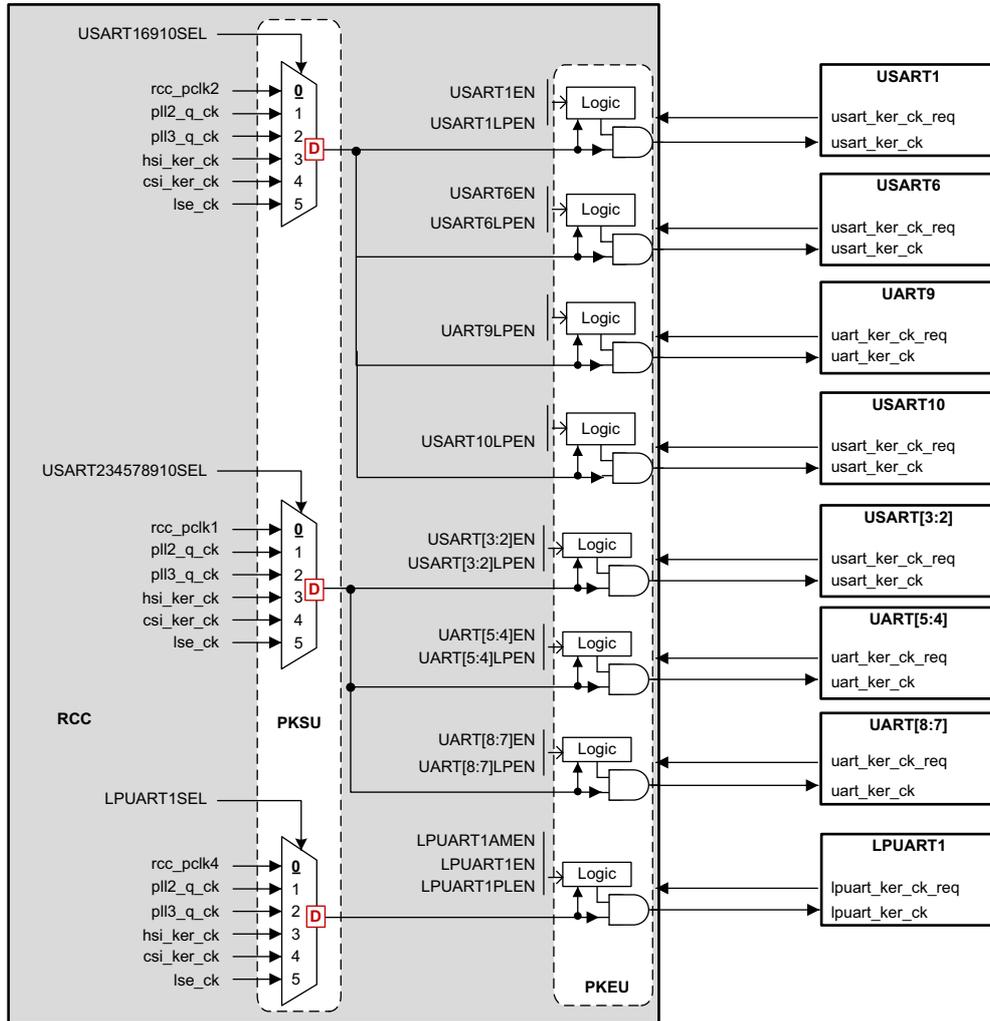
The diagram illustrates the internal clock distribution for various UART, USART, and LPUART1 peripherals. On the left, three multiplexers (MUX) are shown, each with six inputs: rcc_pclk2, pll2_q_ck, pll3_q_ck, hsi_ker_ck, csi_ker_ck, and lse_ck. The first MUX (top) is controlled by USART16910SEL and its output (marked with a red 'D') is connected to a 'Logic' block for USART1. The second MUX (middle) is controlled by USART234578910SEL and its output (marked with a red 'D') is connected to 'Logic' blocks for USART6, USART10, and USART[3:2]. The third MUX (bottom) is controlled by LPUART1SEL and its output (marked with a red 'D') is connected to 'Logic' blocks for UART9, UART10, UART[3:2], UART[5:4], UART[8:7], and LPUART1. Each 'Logic' block consists of an AND gate that combines the selected clock with an enable signal (e.g., USART1EN, USART1LPEN) to produce the final kernel clock (e.g., usart_ker_ck_req, usart_ker_ck). The peripherals are shown on the right: USART1, USART6, UART9, USART10, USART[3:2], UART[5:4], UART[8:7], and LPUART1. The entire diagram is enclosed in a dashed box labeled 'RCC' on the left and 'PKSU' and 'PKEU' at the bottom.
D The switch is dynamic: the transition between two inputs is glitch-free
MSV63811V2
- 1. X represents the selected MUX input after a system reset.
- 2. This figure does not show the connection of the bus interface clock to the peripheral, for details on each enable cell, please refer to Section 8.5.11: Peripheral clock gating control .
Figure 55. Kernel clock distribution for LTDC
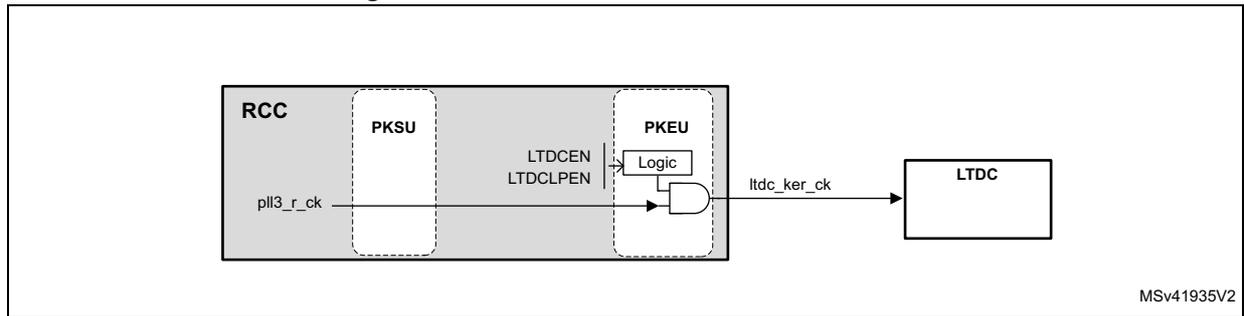
- 1. X represents the selected MUX input after a system reset.
- 2. This figure does not show the connection of the bus interface clock to the peripheral. For details on each enable cell, please refer to Section 8.5.11: Peripheral clock gating control .
- The FMC, OCTOSPI and SDMMC1/2 can also use a clock different from the bus interface clock for more flexibility.
Figure 56. Kernel clock distribution for SDMMC, OCTOSPI and FMC
![Figure 56: Kernel clock distribution for SDMMC, OCTOSPI and FMC. The diagram shows the RCC block with PKSU and PKEU. PKSU contains three MUXes: SDMMCSEL (selecting between pll1_q_ck and pll2_r_ck), OCTOSPISEL (selecting between rcc_hclk3, pll1_q_ck, pll2_r_ck, and per_ck), and FMCSEL (selecting between rcc_hclk3, pll1_q_ck, pll2_r_ck, and per_ck). Selected clocks pass to PKEU, which contains gating logic for each: SDMMC[2:1]EN/LPEN, OCTOSPI[2:1]EN/LPEN, and FMCEN/FMCLPEN. Outputs are sdmmc_ker_ck, octospi_ker_ck, and fmc_ker_ck, feeding SDMMC1/2, OCTOSPI1/2, and FMC blocks respectively. A 'D' icon indicates dynamic glitch-free switching. MSV48160V2](/RM0468-STM32H723-733-725-735-730/83b66fcbd6d4fd6c2eca36952f3bee80_img.jpg)
- 1. X represents the selected MUX input after a system reset.
- 2. This figure does not show the connection of the bus interface clock to the peripheral. For details on each enable cell, please refer to Section 8.5.11: Peripheral clock gating control .
Figure 57 shows the clock distribution for the USB blocks. The USB1ULPI block receives its clock from the external PHY.
The USB1OTG block receives the clock for USB communications which can be selected among different sources thanks to the MUX controlled by USBSEL.
Figure 57. Kernel clock distribution for USB (2)
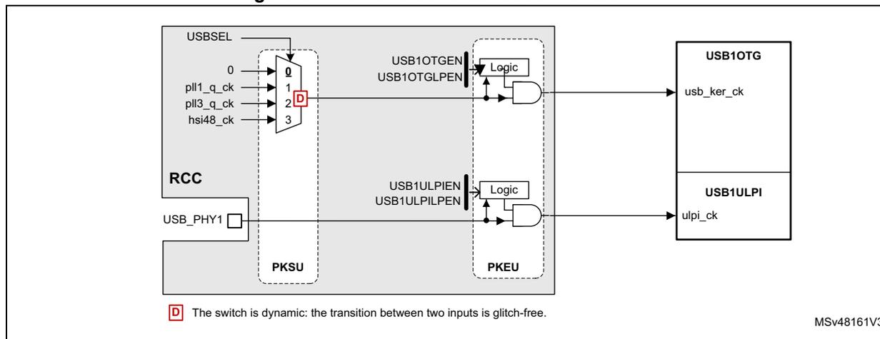
- 1. X represents the selected MUX input after a system reset.
- 2. This figure does not show the connection of the bus interface clock to the peripheral. For details on each enable cell, please refer to Section 8.5.11: Peripheral clock gating control .
The Ethernet transmit and receive clocks shall be provided from an external Ethernet PHY. The clock selection for the RX and TX path is controlled via the SYSCFG block.
Figure 58. Kernel clock distribution for Ethernet
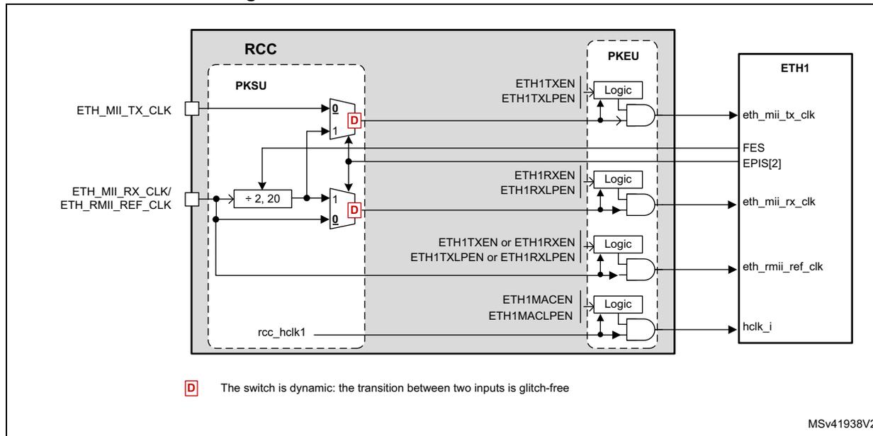
- 1. X represents the selected MUX input after a system reset.
- 2. This figure does not show the connection of the bus interface clock to the peripheral. For details on each enable cell, please refer to Section 8.5.11: Peripheral clock gating control .
Figure 59. Kernel clock distribution for ADCs, SWPMI, RNG and FDCAN (2)
RCC
ADCs:
- ADC3: MUX (ADC3SEL) selects from 0: pll2_p_ck, 1: D (pll3_r_ck), 2: per_ck. Output goes to Logic (inputs: ADC3AMEN, ADC3EN, ADC3LPEN) → adc_ker_ck_input.
- ADC12: MUX (ADC12SEL) selects from 0: pll2_p_ck, 1: D (pll3_r_ck), 2: per_ck. Output goes to Logic (inputs: ADC12EN, ADC12LPEN) → adc_ker_ck_input.
SWPMI:
- SWPMI: MUX (SWPSEL) selects from 0: rcc_pclk1, 1: D (hsi_ker_ck). Output goes to Logic (inputs: SWPEN, SWPLPEN) → swpmi_ker_ck.
RNG:
- RNG: MUX (RNGSEL) selects from 0: hsi48_ck, 1: D (pll1_q_ck), 2: lse_ck, 3: lsi_ck. Output goes to Logic (inputs: RNGEN, RNGLPEN) → rng_ker_ck.
FDCAN:
- FDCAN: MUX (FDCANSEL) selects from 0: hse_ck, 1: D (pll1_q_ck), 2: pll2_q_ck. Output goes to Logic (inputs: FDCANEN, FDCANLPEN) → fdcan_ker_ck.
PKSU (Power Key Switch Unit) and PKEU (Power Key Enable Unit) are shown as functional blocks within the RCC.
D The switch is dynamic: the transition between two inputs is glitch-free
MSV41939V3
- 1. X represents the selected MUX input after a system reset.
- 2. This figure does not show the connection of the bus interface clock to the peripheral. For details on each enable cell, please refer to Section 8.5.11: Peripheral clock gating control .
Figure 60. Kernel clock distribution for LPTIMs and HDMI-CEC (2)
![Schematic diagram of kernel clock distribution for LPTIMs and HDMI-CEC. It shows four clock paths originating from the RCC. 1. HDMI-CEC: lse_ck and lsi_ck are inputs to a 3-to-1 MUX (CECSEL). The output is connected to a Logic block along with CECEN and CECLPEN signals, resulting in cec_ker_ck (im). 2. LPTIM1: rcc_pclk1, pll2_p_ck, pll3_r_ck, lse_ck, lsi_ck, and per_ck are inputs to a 6-to-1 MUX (LPTIM1SEL). The output is connected to a Logic block along with LPTIM1EN and LPTIM1LPEN signals, resulting in lptim_ker_ck. 3. LPTIM2: rcc_pclk4, pll2_p_ck, pll3_r_ck, lse_ck, lsi_ck, and per_ck are inputs to a 6-to-1 MUX (LPTIM2SEL). The output is connected to a Logic block along with LPTIM2AMEN, LPTIM2EN, and LPTIM2LPEN signals, resulting in lptim_ker_ck. 4. LPTIM[5:3]: rcc_pclk4, pll2_p_ck, pll3_r_ck, lse_ck, lsi_ck, and per_ck are inputs to a 6-to-1 MUX (LPTIM345SEL). The output is connected to a Logic block along with LPTIM[5:3]AMEN, LPTIM[5:3]EN, and LPTIM[5:3]LPEN signals, resulting in lptim_ker_ck. The diagram also includes a 'D' symbol indicating dynamic switches and a note about glitch-free transitions. MSv41940V3 is noted in the bottom right.](/RM0468-STM32H723-733-725-735-730/c747f23d3c916cb48bebaa14372b8d75_img.jpg)
- 1. X represents the selected MUX input after a system reset
- 2. This figure does not show the connection of the bus interface clock to the peripheral. For details on each enable cell, please refer to Section 8.5.11: Peripheral clock gating control .
RTC/AWU clock
The rtc_ck clock source can be:
- • the hse_1M_ck ( hse_ck divided by a programmable prescaler)
- • the lse_ck
- • or the lsi_ck clock
The source clock is selected by programming the RTCSEL[1:0] bits in the RCC backup domain control register (RCC_BDCR) and the RTCPRE[5:0] bits in the RCC clock configuration register (RCC_CFGR) .
This selection cannot be modified without resetting the Backup domain.
If the LSE is selected as RTC clock, the RTC will work normally even if the backup or the V DD supply disappears.
The LSE clock is in the Backup domain, whereas the other oscillators are not. As a consequence:
- • If LSE is selected as RTC clock, the RTC continues working even if the \( V_{DD} \) supply is switched OFF, provided the \( V_{BAT} \) supply is maintained.
- • If LSI is selected as the RTC clock, the AWU state is not guaranteed if the \( V_{DD} \) supply is powered off.
- • If the HSE clock is used as RTC clock, the RTC state is not guaranteed if the \( V_{DD} \) supply is powered off or if the \( V_{CORE} \) supply is powered off.
The rtc_ck clock is enabled through RTCEN bit located in the RCC backup domain control register (RCC_BDCR) .
The RTC bus interface clock (APB clock) is enabled through RTCAPBEN and RTCAPBLPEN bits located in RCC_APB4ENR/LPENR registers.
Note: To read the RTC calendar register when the APB clock frequency is less than seven times the RTC clock frequency ( \( F_{APB} < 7 \times F_{RTCLK} \) ), the software must read the calendar time and date registers twice. The data are correct if the second read access to RTC_TR gives the same result than the first one. Otherwise a third read access must be performed.
Watchdog clocks
The RCC provides the clock for the four watchdog blocks available on the circuit. The independent watchdog (IWDG1) is connected to the LSI. The window watchdog (WWDG1) are connected to the APB clock.
If an independent watchdog is started by either hardware option or software access, the LSI is forced ON and cannot be disabled. After the LSI oscillator setup delay, the clock is provided to the IWDG.
Caution: Before enabling the WWDG1, the application must set the WW1RSC bit to 1. If the WW1RSC remains to 0, when the WWDG1 is enabled, its the behavior is not guaranteed. The WW1RSC bit is located in RCC global control register (RCC_GCR) .
Clock frequency measurement using TIMx
Most of the clock source generator frequencies can be measured by means of the input capture of TIMx.
- • Calibrating the HSI or CSI with the LSE
The primary purpose of having the LSE connected to a TIMx input capture is to be able to accurately measure the HSI or CSI. This requires to use the HSI or CSI as system clock source either directly or via PLL1. The number of system clock counts between consecutive edges of the LSE signal gives a measurement of the internal clock period. Taking advantage of the high precision of LSE crystals (typically a few tens of ppm) we can determine the internal clock frequency with the same resolution, and trim the source to compensate for manufacturing-process and/or temperature- and voltage-related frequency deviations.
The basic concept consists in providing a relative measurement (e.g. HSI/LSE ratio): the precision is therefore tightly linked to the ratio between the two clock sources. The greater the ratio is, the more accurate the measurement is.
The HSI and CSI oscillators have dedicated user-accessible calibration bits for this purpose (see RCC CSI configuration register (RCC_CSICFGR) ) for revision Y devices and RCC HSI configuration register (RCC_HSICFGR) / RCC CSI configuration register
( RCC_CS/CFGR ) for revision V devices). When the HSI or CSI are used via the PLLx, the system clock can also be fine-tuned by using the fractional divider of the PLLs.
- • Calibrating the LSI with the HSI
The LSI frequency can also be measured: this is useful for applications that do not have a crystal. The ultra-low power LSI oscillator has a large manufacturing process deviation. By measuring it versus the HSI clock source, it is possible to determine its frequency with the precision of the HSI. The measured value can be used to have more accurate RTC time base timeouts (when LSI is used as the RTC clock source) and/or an IWDG timeout with an acceptable accuracy.
8.5.9 General clock concept overview
The RCC handles the distribution of the CPU, bus interface and peripheral clocks for the system (D1, D2 and D3 domains), according to the operating mode of each function (refer to Section 8.5.1: Clock naming convention for details on clock definitions).
For each peripheral, the application can control the activation/deactivation of its kernel and bus interface clock. Prior to use a peripheral, the CPU has to enable it (by setting PERxEN to 1), and define if this peripheral remains active in CSleep mode (by setting PERxLPEN to 1). This is called 'allocation' of a peripheral to the CPU (refer to Section 8.5.10: Peripheral allocation for more details).
The peripheral allocation is used by the RCC to automatically control the clock gating according to the CPU and domain modes, and by the PWR to control the supply voltages of D1, D2 and D3 domains.
Figure 61 gives an example of peripheral allocation:
- • The CPU enabled SDMMC1, SPI5 and SRAM1, AXISRAM, ITCM, DTCM1, DTCM2 and SRAM4 are implicitly allocated to the CPU. The group composed of the CPU, bus matrix 1/2/3 and allocated peripherals makes up a sub-system (CPU_SS).
Note: The FLASH, AXISRAM, ITCM, DTCM1, DTCM2, SRAM4, IWDG1, PWR, EXTI and RCC are common resources and are implicitly allocated to the CPU.
Figure 61. Peripheral allocation example
Peripherals implicitly allocated to the CPU
MSv63812V1
When the CPU enters CStop mode, the RCC automatically disables the bus interface and kernel clocks of all the peripherals of the CPU_SS as well as the CPU clock. The PLLs, if enabled, are not disabled by the RCC since D3 is still running.
The D3 domain can be kept in DRun mode while the CPU is in CStop mode and D1 and D2 domains are in DStop or DStandby mode. This is done by setting RUN_D3 bit in PWR_CPUCR registers.
- • If RUN_D3 is set to 1, then D3 is maintained in DRun mode, independently from the CPU modes (see PWR_CPUCR register in Section Power control ).
- • If RUN_D3 is set to 0, then D3 domain enters DStop or DStandby mode when the CPU enters CStop mode (see Table 57 ).
Note that the CPU can control if D1, D2 or D3 domains are allowed to enter in DStandby when conditions are met, via bits PDDS_D1, PDDS_D2 and PDDS_D3 of PWR_CPUCR.
A wakeup event will be able to exit D1, D2 and D3 domains from DStandby or DStop mode.
In addition, more autonomy can be given to some peripherals located into D3 domain (refer to Section : D3 domain Autonomous mode for details).
D3 domain Autonomous mode
The Autonomous mode allows to deliver the peripheral clocks to peripherals located in D3, even if the CPU is in CStop mode. When a peripheral has its autonomous bit enabled, it receives its peripheral clocks according to D3 domain state, if the CPU is in CStop mode:
- • If the D3 domain is in DRun mode, peripherals with Autonomous mode activated receive their peripheral clocks,
- • If the D3 domain is in DStop mode, no peripheral clock is provided.
The Autonomous mode does not prevent the D3 domain to enter DStop or DStandby mode.
The autonomous bits are located in RCC D3 Autonomous mode register (RCC_D3AMR) .
For example, the CPU can enter CStop mode, while the SAI4 is filling the SRAM4 with data received from an external device via BDMA. When the amount of received data is reached, the CPU can be activated by a wakeup event. This can be done by setting the SAI4, the BDMA, and SRAM4 in Autonomous mode, while keeping D3 in DRun mode (RUN_D3 set to 1). In this example, the RCC does not switch off the PLLs as the D3 domain is always in DRun mode.
It is possible to go a step further with power consumption reduction by combining the Autonomous mode with the capability of some peripherals (UARTs, I2Cs) to request the kernel clock on their own, without waking-up the CPU. For example, if the system is expecting messages via I2C4, the whole system can be put in Stop mode. When the I2C4 peripheral detects a START bit, it will generate a “kernel clock request”. This request enables the HSI or CSI, and a kernel clock is provided only to the requester (in our example the I2C4). The I2C4 then decodes the incoming message. Several cases are then possible:
- • If the device address of the message does not match, then I2C4 releases its “kernel clock request” until a new START condition is detected.
- • If the device address of the incoming message matches, it has to be stored into D3 local memory. I2C4 is able to generate a wakeup event on address match to switch the D3 domain to DRun mode. The message is then transferred into memory via BDMA, and the D3 domain go back to DStop mode without any CPU activation. Note that if the amount of data transferred into memory reached the transfer count, the BDMA can also generate an interrupt to wake-up the CPU.
- • If the device address of the incoming message matches and the peripheral is setup to wake up the CPU, then I2C4 generates a wakeup event to activate the CPU.
Please refer to the description of EXTI block in order see which peripheral is able to perform a wake-up event to which domain.
Memory handling
The CPU can access all the memory areas available in the product:
- • AXISRAM, ITCM, DTCM1, DTCM2 and FLASH,
- • SRAM1 and SRAM2,
- • SRAM4 and BKPRAM.
As shown in Figure 61 , FLASH, AXISRAM, SRAM4, ITCM, DTCM1 and DTCM2 are implicitly allocated to the CPU. As a result, there is no enable bit allowing the CPU to allocate these memories.
If the CPU wants to use memories located into D2 domain (SRAM1 and SRAM2), it has to enable them.
The BKPRAM has a dedicated enable in order to gate the bus interface clock. The CPU needs to enable the BKPRAM prior to use it.
Note: The memory interface clocks (Flash and RAM interfaces) can be stopped by software during CSleep mode (via DxSRAMyLPEN bits).
Refer to Peripheral clock gating control and CPU and bus matrix clock gating control sections for details on clock enabling.
System states overview
Table 57 gives an overview of the system states with respect to the D1, D2 and D3 domain modes.
- • The system remains in Run mode as long as D3 is in DRun mode. Several sub-states of system Run exist that are not detailed here (refer to Section 6: Power control (PWR) for more information).
- • When the D1 domain is in DRun, the D2 domain can be in DRun, DStop or DStandby. When the D1 domain is in DStop or DStandby, the D2 domain can no longer remain in DRun it will switch to DStop or DStandby according to PDDS_D2 bit.
- • D3 can run while D1 and D2 are in DStop/DStandby mode thanks to RUN_D3 bits of PWR_CPUCR registers or when D3 is in Autonomous mode.
- • The system remains in Stop mode as long as D3 is in DStop mode. This means implicitly that D1 and D2 are in DStop or DStandby. As soon as D1 or D2 exits DStop or DStandby, D3 switches to DRun mode.
- • The system remains in Standby mode as long as D1, D2 and D3 are in DStandby.
- • Domain states versus CPU states:
- – When the D1 domain is in DRun mode, it means that its bus matrix is clocked, and the CPU is in CRun mode.
- – When the D2 domain is in DRun mode, it means that its bus matrix is clocked, and the CPU is in CRun mode with at least a peripheral of D2 domain allocated.
- – When the D1 domain is in DStop mode it means that its bus matrix is no longer clocked, and the CPU is in CStop mode.
- – When the D2 domain is in DStop mode it means that its bus matrix is no longer clocked. This situation happens when:
- - the CPU did not allocate peripherals of D2 domain,
- - the CPU allocated peripherals of D2 domain, but the CPU is in CStop or CStandby,
- – When a domain is in DStandby mode, it means that the domain including its CPU are powered down.
Table 57. System states overview
| System State | D1 State | D2 State | D3 State |
|---|---|---|---|
| Run | DRun | DRun/DStop/DStandby | DRun |
| DStop/DStandby | DStop/DStandby | ||
| Stop | DStop/DStandby | DStop/ DStandby | DStop |
| Standby | DStandby | DStandby | DStandby |
8.5.10 Peripheral allocation
The CPU can allocate a peripheral and hence control its kernel and bus interface clock.
The CPU can allocate a peripheral by setting the dedicated PERxEN bit located into:
- • RCC_xxxxENR registers or
- • RCC_C1_xxxxENR registers.
The CPU can control the peripheral clocks gating when it is in CSleep mode via the PERxLPEN bits located into:
- • RCC_xxxxLPENR registers or
- • RCC_C1_xxxxLPENR registers.
Refer to Section 8.7.1: Register mapping overview for additional information.
The peripheral allocation bits (PERxEN bits) are used by the hardware to provide the kernel and bus interface clocks to the peripherals. However they are also used to link peripherals to the CPU (CPU sub-system). In this way, the hardware is able to safely gate the peripheral clocks and bus matrix clocks according to CPU states. The PWR block also uses this information to control properly the domain states.
Clock switches and gating
- • Clock switching delays
The input selected by the kernel clock switches can be changed dynamically without generating spurs or timing violation. As a consequence, switching from the original to the new input can only be performed if a clock is present on both inputs. If it not the case, no clock will be provided to the peripheral. To recover from this situation, the user has to provide a valid clock to both inputs.
During the transition from one input to another, the kernel clock provided to the peripheral will be gated, in the worst case, during 2 clock cycles of the previously selected clock and 2 clock cycles of the new selected clock. As shown in Figure 62 , both input clocks shall be present during transition time.
Figure 62. Kernel Clock switching
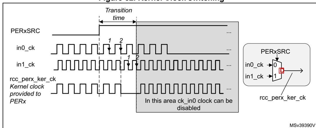
The diagram illustrates the timing for kernel clock switching. The top signal, PERxSRC, is a control signal that switches from a low state to a high state at the beginning of the transition. Below it are two input clocks, in0_ck and in1_ck. in0_ck is initially active, and in1_ck becomes active after the transition. The bottom signal, rcc_perx_ker_ck, is the kernel clock provided to the peripheral. It is shown that during the transition time (marked by two vertical dashed lines), the kernel clock is gated (held low). The diagram indicates that both in0_ck and in1_ck must be present during the transition. A shaded area on the right of the transition indicates that in this area, the ck_in0 clock can be disabled. An inset diagram on the right shows a multiplexer (MUX) with inputs in0_ck (0) and in1_ck (1), controlled by PERxSRC, outputting rcc_perx_ker_ck. The MUX has a red 'D' symbol, indicating a delay or latch.
- • Clock enabling delays
In the same way, the clock gating logic synchronizes the enable command (coming generally from a kernel clock request or PERxEN bits) with the selected clock, in order to avoid generation of spurs.
- – A maximum delay of two periods of the enabled clock may occur between the enable command and the first rising edge of the clock. The enable command can be the rising edge of the PERxEN bits of RCC_xxxxENR registers, or a kernel clock request asserted by a peripheral.
- – A maximum delay of 1.5 periods of the disabled clock may occur between the disable command and the last falling edge of the clock. The disable command can be the falling edge of the PERxEN bits of RCC_xxxxENR registers, or a kernel clock request released by a peripheral.
Note: Both the kernel clock and the bus interface clock are affected by this re-synchronization delay.
In addition, the clock enabling delay may strongly increase if the application is enabling for the first time a peripheral which is not located into the same domain. This is due to the fact that the domain where the peripheral is located could be in DStop or DStandby mode. The domain must be switched to DRun mode before the application can use this peripheral.
As an example, if the CPU enables a peripheral located in the D2 domain while the D2 domain is in DStop/DStandby mode, then the power controller (PWR) has first to provide a supply voltage to D2, then the RCC has to wait for an acknowledge from the PWR before enabling the clocks of the D2 domain. To handle properly this situation the RCC and the PWR blocks feature four flags:
- – D1CKRDY/D2CKRDY located in RCC source control register (RCC_CR)
- – SBF_D1 and SBF_D2 located in PWR_CPUCR register.
The following sequence can be followed to avoid this issue:
- Enable the peripheral clocks (i.e. allocate the peripheral) by writing the corresponding PERxEN bit to 1 in the RCC_xxxxENR register,
- Read back the RCC_xxxxENR register to make sure that the previous write operation is not pending into a write buffer.
- If the peripheral is located in a different domain, perform the two next steps:
Read DxCKRDY until it is set to 1.
Write SBF_Dx to zero and read-back the value, in order to check if the domain where the peripheral is located is still in DStandby. If the corresponding bit is read at 1, it means that the domain is still in DStandby. Repeat this operation until SBF_Dx is equal to 0, then continue the other steps.
- Perform a dummy read operation into a register of the enabled peripheral. This operation will take at least 2 clock cycles, which is equal to the max delay of the enable command.
- The peripheral can then be used.
Note: When the bus interface clock is not active, read or write accesses to the peripheral registers are not supported. A read access will return invalid data. A write access will be ignored and will not create any bus errors.
8.5.11 Peripheral clock gating control
As mentioned previously, each peripheral requires a bus interface clock, named rcc_perx_bus_ck (for peripheral 'x'). This clock can be an APB, AHB or AXI clock, according to which bus the peripheral is connected.
The clocks used as bus interface for peripherals located in D1 domain, could be rcc_aclk , rcc_hclk3 or rcc_pclk3 , depending on the bus connected to each peripheral. For simplicity sake, these clocks are named rcc_bus_d1_ck .
In the same way, the signal named rcc_bus_d2_ck represents rcc_hclk1 , rcc_hclk2 , rcc_pclk1 or rcc_pclk2 , depending on the bus connected to each peripheral of D2 domain.
Similarly, the signal rcc_bus_d3_ck represents rcc_hclk4 or rcc_pclk4 for peripherals located in D3.
Some peripherals (SAI, UART...) also require a dedicated clock for their communication interface. This clock is generally asynchronous with respect to the bus interface clock. It is named kernel clock ( perx_ker_ckreq ). Both clocks can be gated according to several conditions detailed hereafter.
As shown in Figure 63 , enabling the kernel and bus interface clocks of each peripheral depends on several input signals:
- • PERxEN and PERxLPEN bits
PERxEN represents the peripheral enable (allocation) bit for the CPU. The CPU can write these bits to 1 via RCC_C1_xxxxENR or RCC_xxxxENR registers. - • PERxAMEN bits
The PERxAMEN bits are belong to RCC D3 Autonomous mode register (RCC_D3AMR) . - • CPU state ( c_sleep and c_deepsleep signals)
- • D3 domain state ( d3_deepsleep signal)
- • The kernel clock request ( perx_ker_ckreq ) of the peripheral itself, when the feature is available.
Refer to Section 8.5.10: Peripheral allocation for more details.
Figure 63. Peripheral kernel clock enable logic details
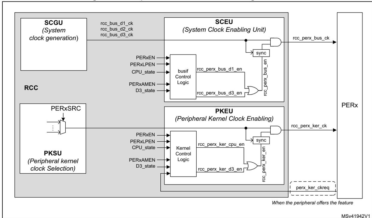
The diagram illustrates the internal clock enable logic for a peripheral (PERx). It is divided into two main paths: the System Clock Enabling Unit (SCEU) and the Peripheral Kernel Clock Enabling (PKEU).
- SCEU (System Clock Enabling Unit):
This unit generates the
rcc_perx_bus_cksignal. It takes inputs from the SCGU (System clock generation) and a busif Control Logic block. The busif Control Logic receivesPERxEN,PERxLPEN,CPU_state,PERxAMEN, andD3_statesignals. The SCEU logic includes a 'sync' block and AND/OR gates to producercc_perx_bus_en, which is then ANDed with the SCGU outputs (rcc_bus_d1_ck,rcc_bus_d2_ck,rcc_bus_d3_ck) to generatercc_perx_bus_ck. - PKEU (Peripheral Kernel Clock Enabling):
This unit generates the
rcc_perx_ker_cksignal. It takes inputs from the PKSU (Peripheral kernel clock Selection) and a Kernel Control Logic block. The Kernel Control Logic receives the same control signals as the busif Control Logic. The PKEU logic includes a 'sync' block and AND/OR gates to producercc_perx_ker_en, which is then ANDed with the PKSU output to generatercc_perx_ker_ck. A dashed box labeledperx_ker_ckreqindicates an optional feature from the peripheral.
When the peripheral offers the feature
MSV41942V1
Table 58 gives a detailed description of the enabling logic of the peripheral clocks for peripherals located in D1 or D2 domain and allocated by the CPU.
Table 58. Peripheral clock enabling for D1 and D2 peripherals
| PERxEN | PERxLPEN | PERxSRC | perx_ker_ckreq | CPU State | rcc_perx_ker_c_en | rcc_perx_bus_d1_en | Comments |
|---|---|---|---|---|---|---|---|
| 0 | X | X | X | X | 0 | 0 | No clock provided to the peripheral, because PERxEN=0 |
| 1 | X | X | X | CRun | 1 | 1 | Kernel and bus interface clocks are provided to the peripheral, because the CPU is in CRun, and PERxEN=1 |
| 1 | 0 | X | X | CSleep | 0 | 0 | No clock provided to the peripheral, because the CPU is in CSleep, and PERxLPEN=0 |
| 1 | 1 | X | X | 1 | 1 | Kernel and bus interface clocks are provided to the peripheral, because CPU is in CSleep, and PERxLPEN=1 | |
| 1 | 0 | X | X | CStop | 0 | 0 | No clock provided to the peripheral because the PERxLPEN bit is set to 0. |
| 1 | 1 | no lsi_ck and no lse_ck and no hsi_ker_ck and no csi_ker_ck | X | 0 | 0 | No clock provided to the peripheral because CPU is in CStop and lse_ck or lsi_ck or hsi_ker_ck or csi_ker_ck are not selected. | |
| 1 | 1 | lsi_ck or lse_ck | X | 1 (1) | 0 | Kernel clock is provided to the peripheral because PERxEN = PERxLPEN=1 and lsi_ck or lse_ck are selected. The bus interface clock is no provided as the CPU is in CStop | |
| 1 | 1 | hsi_ker_ck or csi_ker_ck | 1 | 1 | 0 | Kernel clock is provided to the peripheral because req_ker_perx = 1, and PERxEN = PERxLPEN=1 and hsi_ker_ck or csi_ker_ck are selected. The bus interface clock is no provided as the CPU is in CStop | |
| 1 | 1 | hsi_ker_ck or csi_ker_ck | 0 | 0 | 0 | No clock provided to the peripheral because CPU is in CStop, and no kernel clock request pending |
1. For RNG block, the kernel clock is not delivered if the CPU to which it is allocated is in CStop mode, even if the clock selected is lsi_ck or lse_ck.
As a summary, we can state that the kernel clock is provided to the peripherals located on domains D1 and D2 when the following conditions are met:
- 1. The CPU is in CRun mode, and the peripheral is allocated.
- 2. The CPU is in CSleep mode, and the peripheral is allocated with PERxLPEN = 1.
- 3. The CPU is in CStop mode, and the peripheral is allocated with PERxLPEN = 1, and the peripheral generates a kernel clock request, and the selected clock is hsi_ker_ck or csi_ker_ck .
- 4. The CPU is in CStop mode, and the peripheral is allocated with PERxLPEN = 1, and the kernel source clock of the peripheral is lse_ck or lsi_ck .
The bus interface clock will be provided to the peripherals only when conditions 1 or 2 are met.
Table 59 gives a detailed description of the enabling logic of the kernel clock for all peripherals located in D3.
Table 59. Peripheral clock enabling for D3 peripherals
| PERxEN | PERxLPEN | PERxAMEN | PERxSRC | perx_ker_ckreq | CPU State | D3 State | rcc_perx_ker_d3_en | rcc_perx_bus_d3_en | Comments |
|---|---|---|---|---|---|---|---|---|---|
| 0 | X | X | X | X | Any | Any | 0 | 0 | No clock provided to the peripheral, as PERxEN=0 |
| 1 | X | X | X | X | CRun | 1 | 1 | Kernel and bus interface clocks are provided to the peripheral, because the CPU is in CRun, and PERxEN=1 | |
| 1 | 0 | X | X | X | CSleep | DRun | 0 | 0 | No clock provided to the peripheral, because the CPU is in CSleep, and PERxLPEN=0 |
| 1 | 1 | X | X | X | 1 | 1 | Kernel and bus interface clocks are provided to the peripheral, because the CPU is in CSleep, and PERxLPEN=1 | ||
| 1 | X | 0 | X | X | CStop | 0 | 0 | As the CPU is in CStop, and PERxEN=1, then the kernel clock gating depends on D3 state and PERxAMEN bits. No clock provided to the peripheral because PERxAMEN = 0. | |
| 1 | X | 1 | X | X | 1 | 1 | The kernel and bus interface clocks are provided because even if the CPU is in CStop mode, D3 is in DRun mode, with PERxEN and PERxAMEN bits set to 1. | ||
| 1 | X | 1 | not lse_ck and not lsi_ck | 0 | DStop | 0 | 0 | No clock provided to the peripheral, because D3 is in DStop, req_ker_perx = 0, and lse_ck or lsi_ck are not selected. | |
Table 59. Peripheral clock enabling for D3 peripherals (continued)
| PERxEN | PERxLPEN | PERxAMEN | PERxSRC | perx_ker_ckreq | CPU State | D3 State | rcc_perx_ker_d3_en | rcc_perx_bus_d3_en | Comments |
|---|---|---|---|---|---|---|---|---|---|
| 1 | X | 1 | not hsi_ker_ck and not csi_ker_ck and not lse_ck and not lsi_ck | 1 | 0 | 0 | No clock provided to the peripheral, because even if req_ker_perx = 0, lse_ck or lsi_ck or hsi_ker_ck or csi_ker_ck are not selected. | ||
| 1 | X | 1 | hsi_ker_ck or csi_ker_ck | 1 | 1 | 0 | Kernel clock is provided to the peripheral because
req_ker_perx
= 1, and PERxEN = PERxAMEN=1, and the selected clock is
hsi_ker_ck
or
csi_ker_ck
. The bus interface clock is not provided as D3 is in DStop. | ||
| 1 | X | 1 | lse_ck or lsi_ck | X | 1 | 0 | Kernel clock is provided to the peripheral because PERxEN = PERxAMEN=1 and
lse_ck
or
lsi_ck
are selected, while D3 is in STOP. The bus interface clock is not provided as D3 is in DSTOP. |
As a summary, we can state that the kernel clock is provided to the peripherals of D3 if the following conditions are met:
- 1. The CPU is in CRun mode, and the peripheral is allocated.
- 2. The CPU is in CSleep mode, and the peripheral is allocated with PERxLPEN = 1.
- 3. The CPU is in CStop mode, and the peripheral is allocated and D3 domain is in DRun mode with PERxAMEN = 1.
- 4. The CPU is in CStop mode, and the peripheral is allocated, and D3 domain is in DStop mode with PERxAMEN = 1, and the peripheral is generating a kernel clock request and the kernel clock source is hsi_ker_ck or csi_ker_ck .
- 5. The CPU is in CStop mode, and the peripheral is allocated, and D3 domain is in DStop mode with PERxAMEN = 1, and the kernel clock source of the peripheral is lse_ck or lsi_ck .
The bus interface clock will be provided to the peripherals only when condition 1, 2 or 3 is met.
Note: When they are set to 1, the autonomous bits indicate that the associated peripheral will receive a kernel clock according to D3 state, and not according to the mode of the CPU.
Only I2C, U(S)ART and LPUART peripherals are able to request the kernel clock. This feature gives to the peripheral the capability to transfer data with an optimal power consumption.
The autonomous bits dedicated to some peripherals located in D3 domain allow the data transfer with external devices without activating the CPU.
In order for the LPTIMER to operate with lse_ck or lsi_ck when the circuit is in Stop mode, the user application has to select the lsi_ck or lse_ck input via LPTIMxSEL fields, and set bit LPTIMxAMEN and LPTIMxLPEN to 1.
8.5.12 CPU and bus matrix clock gating control
For each domain it is possible to control the activation/deactivation of the CPU clock and bus matrix clock.
For information about convention naming, refer to Section 8.5.11: Peripheral clock gating control .
The clocks of the CPU, AHB and AXI bridges and APB busses are enabled according to the rules hereafter:
- • The CPU clock rcc_c_ck is enabled when the CPU is in CRun mode.
- • The AXI bridge clock is enabled when the CPU is in CRun mode.
- • The D2 domain AHB bridges clocks are enabled when:
- – The CPU is in CRun or,
- – If the CPU is in CSleep with at least a peripheral (master) connected to this bus having both its PERxEN and PERxLPEN set to 1 or,
- – If the CPU is in CSleep with at least an APB bus having its clock enabled.
- • The D3 domain AHB bridge clock is enabled when:
- – The CPU is in CRun or CSleep mode or,
- – When the RUN_D3 bit is set to 1, independently of CPU modes or,
- – When the d3_deepsleep signal is inactive (0), independently of CPU modes.
- • The APB1,2,3 busses are enabled when:
- – The CPU is in CRun or,
- – If the CPU is in CSleep with at least a peripheral connected to this bus having both its PERxEN and PERxLPEN set to 1.
- • The APB4 bus is enabled when: the D3 domain is in DRun.
As shown in the Figure 64 , the enabling of the core and bus clock of each domain depends on several input signals:
- • c_sleep and c_deepsleep signals from the CPU,
- • d3_sleepdeep signal,
- • RCC_xxxxENR.PERxEN bits of peripherals located on D2 domain
Figure 64. Bus clock enable logic
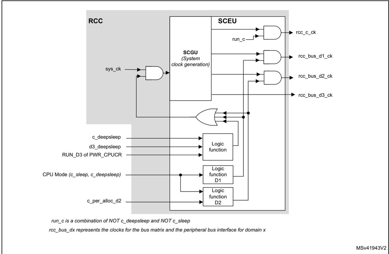
The diagram illustrates the bus clock enable logic. On the left, the RCC block contains an AND gate that takes sys_ck and a signal from the SCGU as inputs. The output of this AND gate is connected to the SCEU block and also to one input of an OR gate. The SCGU (System clock generation) block is connected to the SCEU block. The SCEU block contains four AND gates that generate the following outputs: rcc_c_ck , rcc_bus_d1_ck , rcc_bus_d2_ck , and rcc_bus_d3_ck . The rcc_c_ck output is also connected to the OR gate. The OR gate's output is connected to three logic functions: Logic function , Logic function D1 , and Logic function D2 . These logic functions take various inputs: c_deepsleep , d3_deepsleep , RUN_D3 of PWR_CPUCR , CPU Mode (c_sleep, c_deepsleep) , and c_per_alloc_d2 . The outputs of these logic functions are connected to the inputs of the AND gates in the SCEU block. A note at the bottom left states: run_c is a combination of NOT c_deepsleep and NOT c_sleep . Another note states: rcc_bus_dx represents the clocks for the bus matrix and the peripheral bus interface for domain x . The diagram is labeled with MSV41943V2 in the bottom right corner.
8.6 RCC Interrupts
The RCC provides 3 interrupt lines:
- • rcc_it : a general interrupt line, providing events when the PLLs are ready, or when the oscillators are ready.
- • rcc_hsecss_it : an interrupt line dedicated to the failure detection of the HSE Clock Security System.
- • rcc_lsecss_it : an interrupt line dedicated to the failure detection of the LSE Clock Security System.
The interrupt enable is controlled via RCC clock source interrupt enable register (RCC_CIER) , except for the HSE CSS failure. When the HSE CSS feature is enabled, it not possible to mask the interrupt generation.
The interrupt flags can be checked via RCC clock source interrupt flag register (RCC_CIFR) , and those flags can be cleared via RCC clock source interrupt clear register (RCC_CICR) .
Note: The interrupt flags are not relevant if the corresponding interrupt enable bit is not set.
Table 60 gives a summary of the interrupt sources, and the way to control them.
Table 60. Interrupt sources and control
| Interrupt Source | Description | Interrupt enable | Action to clear interrupt | Interrupt Line |
|---|---|---|---|---|
| LSIRDYF | LSI ready | LSIRDYIE | Set LSIRDYC to 1 | rcc_it |
| LSERDYF | LSE ready | LSERDYIE | Set LSERDYC to 1 | |
| HSIDRYF | HSI ready | HSIDRYIE | Set HSIRDYC to 1 | |
| HSERDYF | HSE ready | HSERDYIE | Set HSERDYC to 1 | |
| CSIRDYF | CSI ready | CSIRDYIE | Set CSIRDYC to 1 | |
| HSI48RDYF | HSI48 ready | HSI48RDYIE | Set HSI48RDYC to 1 | |
| PLL1RDYF | PLL1 ready | PLL1RDYIE | Set PLL1RDYC to 1 | |
| PLL2RDYF | PLL2 ready | PLL2RDYIE | Set PLL2RDYC to 1 | |
| PLL3RDYF | PLL3 ready | PLL3RDYIE | Set PLL3RDYC to 1 | |
| LSECSSF | LSE Clock security system failure | LSECSSFIE (1) | Set LSECSSC to 1 | rcc_lsecss_it |
| HSECSSF | HSE Clock security system failure | -( 2 ) | Set HSECSSC to 1 | rcc_hsecss_it |
1. The security system feature must also be enabled (LSECSSON = 1), in order to generate interrupts.
2. It is not possible to mask this interrupt when the security system feature is enabled (HSECSSON = 1).
8.7 RCC registers
8.7.1 Register mapping overview
Note that the control of PERxEN and PERxLPEN bits can be performed at two different address offset: 0x0D0 and 0x130. So the application can use the registers named:
- • RCC_xxxENR or RCC_C1_xxxENR to control the PERxEN bits
- • RCC_xxxLPENR or RCC_C1_xxxLPENR to control the PERxLPEN bits
- • RCC_RSR or RCC_C1_RSR to control the reset flag status bits.
This feature is provided to insure the compatibility with other products of this family.
Figure 65 shows the RCC mapping overview.
Figure 65. RCC mapping overview
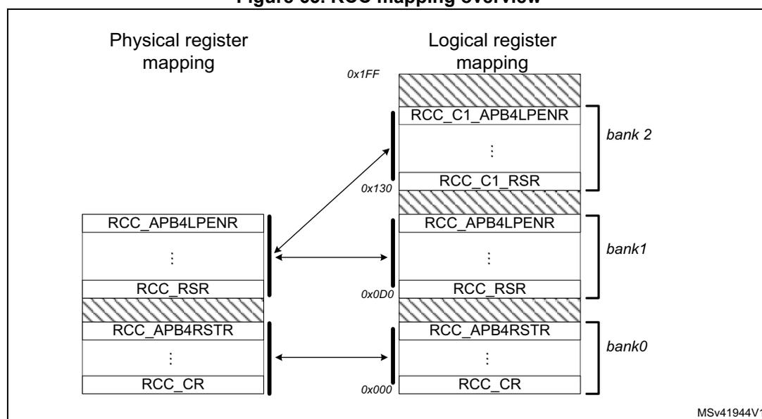
The diagram illustrates the mapping of RCC registers between physical and logical address spaces. It is divided into two main columns: 'Physical register mapping' on the left and 'Logical register mapping' on the right.
Physical register mapping: This column shows a vertical stack of registers starting from address 0x000 at the bottom. The registers are: RCC_CR, followed by a vertical ellipsis, then RCC_APB4RSTR, RCC_RSR (highlighted with diagonal hatching), another vertical ellipsis, and RCC_APB4LPENR at the top. An arrow points from the top register (RCC_APB4LPENR) to the address 0x130 on the logical side.
Logical register mapping: This column shows registers at two different address ranges. The first range starts at 0x000 and includes RCC_CR, a vertical ellipsis, RCC_APB4RSTR, RCC_RSR (hatched), and RCC_APB4LPENR. The second range starts at 0x130 and includes RCC_C1_RSR (hatched), a vertical ellipsis, and RCC_C1_APB4LPENR. Arrows indicate the mapping: from 0x000 to 0x000, from 0x130 to 0x130, and from the physical top register to the logical top register.
Banking: The logical registers are grouped into three banks: 'bank 0' (RCC_CR to RCC_APB4RSTR), 'bank 1' (RCC_RSR to RCC_APB4LPENR), and 'bank 2' (RCC_C1_RSR to RCC_C1_APB4LPENR). The address 0x1FF is indicated at the top of the logical mapping.
The diagram is labeled with 'MSV41944V1' in the bottom right corner.
8.7.2 RCC source control register (RCC_CR)
Address offset: 0x000
Reset value: 0x0000 0001
| 31 | 30 | 29 | 28 | 27 | 26 | 25 | 24 | 23 | 22 | 21 | 20 | 19 | 18 | 17 | 16 |
|---|---|---|---|---|---|---|---|---|---|---|---|---|---|---|---|
| Res. | Res. | PLL3RDY | PLL3ON | PLL2RDY | PLL2ON | PLL1RDY | PLL1ON | Res. | Res. | Res. | Res. | HSEOCSSON | HSEBYP | HSERDY | HSEON |
| r | rw | r | rw | r | rw | rs | rw | r | rw | ||||||
| 15 | 14 | 13 | 12 | 11 | 10 | 9 | 8 | 7 | 6 | 5 | 4 | 3 | 2 | 1 | 0 |
| D2CKRDY | D1CKRDY | HSI48RDY | HSI48ON | Res. | Res. | CSIKERON | CSIRDY | CSION | Res. | HSIDIVF | HSIDIV[1:0] | rw | HSIRDY | HSIKERON | HSION |
| r | r | r | rw | rw | r | rw | r | r | rw | rw |
Bits 31:30 Reserved, must be kept at reset value.
Bit 29 PLL3RDY : PLL3 clock ready flag
Set by hardware to indicate that the PLL3 is locked.
0: PLL3 unlocked (default after reset)
1: PLL3 locked
Bit 28 PLL3ON : PLL3 enable
Set and cleared by software to enable PLL3.
Cleared by hardware when entering Stop or Standby mode.
0: PLL3 OFF (default after reset)
1: PLL3 ON
Bit 27 PLL2RDY : PLL2 clock ready flag
Set by hardware to indicate that the PLL2 is locked.
0: PLL2 unlocked (default after reset)
1: PLL2 locked
Bit 26 PLL2ON : PLL2 enable
Set and cleared by software to enable PLL2.
Cleared by hardware when entering Stop or Standby mode.
0: PLL2 OFF (default after reset)
1: PLL2 ON
Bit 25 PLL1RDY : PLL1 clock ready flag
Set by hardware to indicate that the PLL1 is locked.
0: PLL1 unlocked (default after reset)
1: PLL1 locked
Bit 24 PLL1ON : PLL1 enable
Set and cleared by software to enable PLL1.
Cleared by hardware when entering Stop or Standby mode. Note that the hardware prevents writing this bit to 0, if the PLL1 output is used as the system clock.
0: PLL1 OFF (default after reset)
1: PLL1 ON
Bits 23:20 Reserved, must be kept at reset value.
Bit 19 HSECSSON: HSE Clock Security System enableSet by software to enable Clock Security System on HSE.
This bit is “set only” (disabled by a system reset or when the system enters in Standby mode).
When HSECSSON is set, the clock detector is enabled by hardware when the HSE is ready and disabled by hardware if an oscillator failure is detected.
This bit can be cleared by software, but clearing this bit through software has no impact on the feature.
0: Clock Security System on HSE OFF (Clock detector OFF) (default after reset)
1: Clock Security System on HSE ON (Clock detector ON if the HSE oscillator is stable, OFF if not).
Bit 18 HSEBYP: HSE clock bypassSet and cleared by software to bypass the oscillator with an external clock. The external clock must be enabled with the HSEON bit, to be used by the device.
The HSEBYP bit can be written only if the HSE oscillator is disabled.
0: HSE oscillator not bypassed (default after reset)
1: HSE oscillator bypassed with an external clock
Bit 17 HSERDY: HSE clock ready flagSet by hardware to indicate that the HSE oscillator is stable.
0: HSE clock is not ready (default after reset)
1: HSE clock is ready
Bit 16 HSEON: HSE clock enableSet and cleared by software.
Cleared by hardware to stop the HSE when entering Stop or Standby mode.
This bit cannot be cleared if the HSE is used directly (via SW mux) as system clock or if the HSE is selected as reference clock for PLL1 with PLL1 enabled (PLL1ON bit set to 1).
0: HSE is OFF (default after reset)
1: HSE is ON
Bit 15 D2CKRDY: D2 domain clocks ready flagSet by hardware to indicate that the D2 domain clocks are available.
0: D2 domain clocks are not available (default after reset)
1: D2 domain clocks are available
Bit 14 D1CKRDY: D1 domain clocks ready flagSet by hardware to indicate that the D1 domain clocks (CPU, bus and peripheral) are available.
0: D1 domain clocks are not available (default after reset)
1: D1 domain clocks are available
Bit 13 HSI48RDY: HSI48 clock ready flagSet by hardware to indicate that the HSI48 oscillator is stable.
0: HSI48 clock is not ready (default after reset)
1: HSI48 clock is ready
Bit 12 HSI48ON: HSI48 clock enableSet by software and cleared by software or by the hardware when the system enters to Stop or Standby mode.
0: HSI48 is OFF (default after reset)
1: HSI48 is ON
Bits 11:10 Reserved, must be kept at reset value.
Bit 9 CSIKERON : CSI clock enable in Stop modeSet and reset by software to force the CSI to ON, even in Stop mode, in order to be quickly available as kernel clock for some peripherals. This bit has no effect on the value of CSION.
0: no effect on CSI (default after reset)
1: CSI is forced to ON even in Stop mode
Bit 8 CSIRDY : CSI clock ready flagSet by hardware to indicate that the CSI oscillator is stable. This bit is activated only if the RC is enabled by CSION (it is not activated if the CSI is enabled by CSIKERON or by a peripheral request).
0: CSI clock is not ready (default after reset)
1: CSI clock is ready
Bit 7 CSION : CSI clock enableSet and reset by software to enable/disable CSI clock for system and/or peripheral.
Set by hardware to force the CSI to ON when the system leaves Stop mode, if STOPWUCK = 1 or STOPKERWUCK = 1.
This bit cannot be cleared if the CSI is used directly (via SW mux) as system clock or if the CSI is selected as reference clock for PLL1 with PLL1 enabled (PLL1ON bit set to 1).
0: CSI is OFF (default after reset)
1: CSI is ON
Bit 6 Reserved, must be kept at reset value.
Bit 5 HSIDIVF : HSI divider flagSet and reset by hardware.
As a write operation to HSIDIV has not an immediate effect on the frequency, this flag indicates the current status of the HSI divider. HSIDIVF will go immediately to 0 when HSIDIV value is changed, and will be set back to 1 when the output frequency matches the value programmed into HSIDIV.
0: new division ratio not yet propagated to hsi(_ker)_ck (default after reset)
1: hsi(_ker)_ck clock frequency reflects the new HSIDIV value
Bits 4:3 HSIDIV[1:0] : HSI clock dividerSet and reset by software.
These bits allow selecting a division ratio in order to configure the wanted HSI clock frequency. The HSIDIV cannot be changed if the HSI is selected as reference clock for at least one enabled PLL (PLLxON bit set to 1). In that case, the new HSIDIV value is ignored.
00: Division by 1, hsi(_ker)_ck = 64 MHz (default after reset)
01: Division by 2, hsi(_ker)_ck = 32 MHz
10: Division by 4, hsi(_ker)_ck = 16 MHz
11: Division by 8, hsi(_ker)_ck = 8 MHz
Bit 2 HSIRDY: HSI clock ready flagSet by hardware to indicate that the HSI oscillator is stable.
0: HSI clock is not ready (default after reset)
1: HSI clock is ready
Bit 1 HSIKERON: High Speed Internal clock enable in Stop modeSet and reset by software to force the HSI to ON, even in Stop mode, in order to be quickly available as kernel clock for peripherals. This bit has no effect on the value of HSION.
0: no effect on HSI (default after reset)
1: HSI is forced to ON even in Stop mode
Bit 0 HSION: High Speed Internal clock enableSet and cleared by software.
Set by hardware to force the HSI to ON when the product leaves Stop mode, if STOPWUCK = 0 or STOPKERWUCK = 0.
Set by hardware to force the HSI to ON when the product leaves Standby mode or in case of a failure of the HSE which is used as the system clock source.
This bit cannot be cleared if the HSI is used directly (via SW mux) as system clock or if the HSI is selected as reference clock for PLL1 with PLL1 enabled (PLL1ON bit set to 1).
0: HSI is OFF
1: HSI is ON (default after reset)
8.7.3 RCC HSI configuration register (RCC_HSICFGR)
Address offset: 0x004
Reset value: 0x4000 0XXX
| 31 | 30 | 29 | 28 | 27 | 26 | 25 | 24 | 23 | 22 | 21 | 20 | 19 | 18 | 17 | 16 |
|---|---|---|---|---|---|---|---|---|---|---|---|---|---|---|---|
| Res. | HSITRIM[6:0] | Res. | Res. | Res. | Res. | Res. | Res. | Res. | Res. | ||||||
| rw | rw | rw | rw | rw | rw | rw | |||||||||
| 15 | 14 | 13 | 12 | 11 | 10 | 9 | 8 | 7 | 6 | 5 | 4 | 3 | 2 | 1 | 0 |
| Res. | Res. | Res. | Res. | HSICAL[11:0] | |||||||||||
| r | r | r | r | r | r | r | r | r | r | r | r | ||||
Bit 31 Reserved, must be kept at reset value.
Bits 30:24 HSITRIM[6:0] : HSI clock trimming
Set by software to adjust calibration.
HSITRIM field is added to the engineering Option Bytes loaded during reset phase (FLASH_HSI_opt) in order to form the calibration trimming value.
\( HSICAL = HSITRIM + FLASH\_HSI\_opt \) .
Note: The reset value of the field is 0x40.
Bits 23:12 Reserved, must be kept at reset value.
Bits 11:0 HSICAL[11:0] : HSI clock calibration
Set by hardware by option byte loading during system reset nreset .
Adjusted by software through trimming bits HSITRIM.
This field represents the sum of engineering Option Byte calibration value and HSITRIM bits value.
8.7.4 RCC clock recovery RC register (RCC_CRRCR)
Address offset: 0x008
Reset value: 0x0000 0XXX
| 31 | 30 | 29 | 28 | 27 | 26 | 25 | 24 | 23 | 22 | 21 | 20 | 19 | 18 | 17 | 16 |
|---|---|---|---|---|---|---|---|---|---|---|---|---|---|---|---|
| Res. | Res. | Res. | Res. | Res. | Res. | Res. | Res. | Res. | Res. | Res. | Res. | Res. | Res. | Res. | Res. |
| 15 | 14 | 13 | 12 | 11 | 10 | 9 | 8 | 7 | 6 | 5 | 4 | 3 | 2 | 1 | 0 |
| Res. | Res. | Res. | Res. | Res. | Res. | HSI48CAL[9:0] | |||||||||
| r | r | r | r | r | r | r | r | r | r | ||||||
Bits 31:10 Reserved, must be kept at reset value.
Bits 9:0 HSI48CAL[9:0] : Internal RC 48 MHz clock calibration
Set by hardware by option byte loading during system reset nreset .
Read-only.
8.7.5 RCC CSI configuration register (RCC_CSICFGR)
Address offset: 0x00C
Reset value: 0x2000 0XXX
| 31 | 30 | 29 | 28 | 27 | 26 | 25 | 24 | 23 | 22 | 21 | 20 | 19 | 18 | 17 | 16 |
|---|---|---|---|---|---|---|---|---|---|---|---|---|---|---|---|
| Res. | Res. | CSITRIM[5:0] | Res. | Res. | Res. | Res. | Res. | Res. | Res. | Res. | |||||
| rw | rw | rw | rw | rw | rw | ||||||||||
| 15 | 14 | 13 | 12 | 11 | 10 | 9 | 8 | 7 | 6 | 5 | 4 | 3 | 2 | 1 | 0 |
| Res. | Res. | Res. | Res. | Res. | Res. | CSICAL[9:0] | |||||||||
| r | r | r | r | r | r | r | r | r | r | ||||||
Bits 31:30 Reserved, must be kept at reset value.
Bits 29:24 CSITRIM[5:0] : CSI clock trimming
Set by software to adjust calibration.
CSITRIM bitfield is added to the engineering option bytes loaded during the reset phase (FLASH_CSI_opt) in order to build the calibration trimming value.
CSICAL = CSITRIM + FLASH_CSI_opt.
Note: The reset value of this bitfield is 0x10.
Bits 23:8 Reserved, must be kept at reset value.
Bits 9:0 CSICAL[9:0] : CSI clock calibration
Set by hardware by option byte loading during system reset nreset .
Adjusted by software through trimming bits CSITRIM.
This bitfield represents the sum of the engineering option byte calibration value and CSITRIM value.
8.7.6 RCC clock configuration register (RCC_CFGR)
Address offset: 0x010
Reset value: 0x0000 0000
| 31 | 30 | 29 | 28 | 27 | 26 | 25 | 24 | 23 | 22 | 21 | 20 | 19 | 18 | 17 | 16 |
|---|---|---|---|---|---|---|---|---|---|---|---|---|---|---|---|
| MCO2[2:0] | MCO2PRE[3:0] | MCO1[2:0] | MCO1PRE[3:0] | Res. | Res. | ||||||||||
| rw | rw | rw | rw | rw | rw | rw | rw | rw | rw | rw | rw | rw | rw | ||
| 15 | 14 | 13 | 12 | 11 | 10 | 9 | 8 | 7 | 6 | 5 | 4 | 3 | 2 | 1 | 0 |
| TIMPRE | Res. | RTCPRE[5:0] | STOPKERWUICK | STOPWUICK | SWS[2:0] | SW[2:0] | |||||||||
| rw | rw | rw | rw | rw | rw | rw | rw | r | r | r | rw | rw | rw | ||
Bits 31:29 MCO2[2:0]: Micro-controller clock output 2
Set and cleared by software. Clock source selection may generate glitches on MCO2.
It is highly recommended to configure these bits only after reset, before enabling the external oscillators and the PLLs.
000: System clock selected ( sys_ck ) (default after reset)
001: PLL2 oscillator clock selected ( pll2_p_ck )
010: HSE clock selected ( hse_ck )
011: PLL1 clock selected ( pll1_p_ck )
100: CSI clock selected ( csi_ck )
101: LSI clock selected ( lsi_ck )
others: reserved
Bits 28:25 MCO2PRE[3:0]: MCO2 prescaler
Set and cleared by software to configure the prescaler of the MCO2. Modification of this prescaler may generate glitches on MCO2. It is highly recommended to change this prescaler only after reset, before enabling the external oscillators and the PLLs.
0000: prescaler disabled (default after reset)
0001: division by 1 (bypass)
0010: division by 2
0011: division by 3
0100: division by 4
...
1111: division by 15
Bits 24:22 MCO1[2:0]: Micro-controller clock output 1
Set and cleared by software. Clock source selection may generate glitches on MCO1.
It is highly recommended to configure these bits only after reset, before enabling the external oscillators and the PLLs.
000: HSI clock selected ( hsi_ck ) (default after reset)
001: LSE oscillator clock selected ( lse_ck )
010: HSE clock selected ( hse_ck )
011: PLL1 clock selected ( pll1_q_ck )
100: HSI48 clock selected ( hsi48_ck )
others: reserved
Bits 21:18 MCO1PRE[3:0] : MCO1 prescaler
Set and cleared by software to configure the prescaler of the MCO1. Modification of this prescaler may generate glitches on MCO1. It is highly recommended to change this prescaler only after reset, before enabling the external oscillators and the PLLs.
0000: prescaler disabled (default after reset)
0001: division by 1 (bypass)
0010: division by 2
0011: division by 3
0100: division by 4
...
1111: division by 15
Bits 17:16 Reserved, must be kept at reset value.
Bit 15 TIMPRE : Timers clocks prescaler selection
This bit is set and reset by software to control the clock frequency of all the timers connected to APB1 and APB2 domains.
0: The Timers kernel clock is equal to rcc_hclk1 if D2PPREx is corresponding to division by 1 or 2, else it is equal to \( 2 \times F_{\text{rcc\_pclkx\_d2}} \) (default after reset)
1: The Timers kernel clock is equal to rcc_hclk1 if D2PPREx is corresponding to division by 1, 2 or 4, else it is equal to \( 4 \times F_{\text{rcc\_pclkx\_d2}} \)
Please refer to Table 53: Ratio between clock timer and pclk
Bit 14 Reserved, must be kept at reset value.
Bits 13:8 RTCPRE[5:0] : HSE division factor for RTC clock
Set and cleared by software to divide the HSE to generate a clock for RTC.
Caution: The software has to set these bits correctly to ensure that the clock supplied to the RTC is lower than 1 MHz. These bits must be configured if needed before selecting the RTC clock source.
000000: no clock (default after reset)
000001: no clock
000010: HSE/2
000011: HSE/3
000100: HSE/4
...
111110: HSE/62
111111: HSE/63
Bit 7 STOPKERWUCK : Kernel clock selection after a wake up from system Stop
Set and reset by software to select the Kernel wakeup clock from system Stop.
0: The HSI is selected as wake up clock from system Stop (default after reset)
1: The CSI is selected as wake up clock from system Stop
See Section 8.5.7: Handling clock generators in Stop and Standby mode for details.
Bit 6 STOPWUCK : System clock selection after a wake up from system Stop
Set and reset by software to select the system wakeup clock from system Stop.
The selected clock is also used as emergency clock for the Clock Security System on HSE.
0: The HSI is selected as wake up clock from system Stop (default after reset)
1: The CSI is selected as wake up clock from system Stop
See Section 8.5.7: Handling clock generators in Stop and Standby mode for details.
Caution: STOPWUCK must not be modified when the Clock Security System is enabled (by HSECSSON bit) and the system clock is HSE (SWS="10") or a switch on HSE is requested (SW="10").
Bits 5:3 SWS[2:0] : System clock switch status
Set and reset by hardware to indicate which clock source is used as system clock.
000: HSI used as system clock ( hsi_ck ) (default after reset)
001: CSI used as system clock ( csi_ck )
010: HSE used as system clock ( hse_ck )
011: PLL1 used as system clock ( pll1_p_ck )
others: Reserved
Bits 2:0 SW[2:0] : System clock switch
Set and reset by software to select system clock source ( sys_ck ).
Set by hardware in order to:
- – force the selection of the HSI or CSI (depending on STOPWUCK selection) when leaving a system Stop mode
- – force the selection of the HSI in case of failure of the HSE when used directly or indirectly as system clock.
000: HSI selected as system clock ( hsi_ck ) (default after reset)
001: CSI selected as system clock ( csi_ck )
010: HSE selected as system clock ( hse_ck )
011: PLL1 selected as system clock ( pll1_p_ck )
others: Reserved
8.7.7 RCC domain 1 clock configuration register (RCC_D1CFGR)
Address offset: 0x018
Reset value: 0x0000 0000
| 31 | 30 | 29 | 28 | 27 | 26 | 25 | 24 | 23 | 22 | 21 | 20 | 19 | 18 | 17 | 16 |
|---|---|---|---|---|---|---|---|---|---|---|---|---|---|---|---|
| Res. | Res. | Res. | Res. | Res. | Res. | Res. | Res. | Res. | Res. | Res. | Res. | Res. | Res. | Res. | Res. |
| 15 | 14 | 13 | 12 | 11 | 10 | 9 | 8 | 7 | 6 | 5 | 4 | 3 | 2 | 1 | 0 |
| Res. | Res. | Res. | Res. | D1CPRE[3:0] | Res. | D1PPRE[2:0] | HPRE[3:0] | ||||||||
| rw | rw | rw | rw | rw | rw | rw | rw | rw | rw | rw | |||||
Bits 31:12 Reserved, must be kept at reset value.
Bits 11:8 D1CPRE[3:0] : D1 domain Core prescaler
Set and reset by software to control D1 domain CPU clock division factor.
Changing this division ratio has an impact on the frequency of the CPU clock, and all bus matrix clocks.
The clocks are divided by the new prescaler factor. This factor ranges from 1 to 16 periods of the slowest APB clock among rcc_pclk[4:1] after D1CPRE update. The application can check if the new division factor is taken into account by reading back this register.
0xxx: sys_ck not divided (default after reset)
1000: sys_ck divided by 2
1001: sys_ck divided by 4
1010: sys_ck divided by 8
1011: sys_ck divided by 16
1100: sys_ck divided by 64
1101: sys_ck divided by 128
1110: sys_ck divided by 256
1111: sys_ck divided by 512
Bit 7 Reserved, must be kept at reset value.
Bits 6:4 D1PPRE[2:0] : D1 domain APB3 prescaler
Set and reset by software to control the division factor of rcc_pclk3 .
The clock is divided by the new prescaler factor from 1 to 16 cycles of rcc_hclk3 after D1PPRE write.
- 0xx: rcc_pclk3 = rcc_hclk3 (default after reset)
- 100: rcc_pclk3 = rcc_hclk3 / 2
- 101: rcc_pclk3 = rcc_hclk3 / 4
- 110: rcc_pclk3 = rcc_hclk3 / 8
- 111: rcc_pclk3 = rcc_hclk3 / 16
Bits 3:0 HPRE[3:0] : D1 domain AHB prescaler
Set and reset by software to control the division factor of rcc_hclk3 and rcc_aclk . Changing this division ratio has an impact on the frequency of all bus matrix clocks.
- 0xxx: rcc_hclk3 = sys_d1cpres_ck (default after reset)
- 1000: rcc_hclk3 = sys_d1cpres_ck / 2
- 1001: rcc_hclk3 = sys_d1cpres_ck / 4
- 1010: rcc_hclk3 = sys_d1cpres_ck / 8
- 1011: rcc_hclk3 = sys_d1cpres_ck / 16
- 1100: rcc_hclk3 = sys_d1cpres_ck / 64
- 1101: rcc_hclk3 = sys_d1cpres_ck / 128
- 1110: rcc_hclk3 = sys_d1cpres_ck / 256
- 1111: rcc_hclk3 = sys_d1cpres_ck / 512
Note: The clocks are divided by the new prescaler factor from 1 to 16 periods of the slowest APB clock among rcc_pclk[4:1] after HPRE update.
Note: Note also that rcc_hclk3 = rcc_aclk .
Caution: Care must be taken when using the voltage scaling. Due to the propagation delay of the new division factor, after a prescaler factor change and before lowering the \( V_{CORE} \) voltage, this register must be read in order to check that the new prescaler value has been taken into account.
Depending on the clock source frequency and the voltage range, the software application has to program a correct value in HPRE to make sure that the system frequency does not exceed the maximum frequency.
8.7.8 RCC domain 2 clock configuration register (RCC_D2CFGR)
Address offset: 0x01C
Reset value: 0x0000 0000
| 31 | 30 | 29 | 28 | 27 | 26 | 25 | 24 | 23 | 22 | 21 | 20 | 19 | 18 | 17 | 16 |
|---|---|---|---|---|---|---|---|---|---|---|---|---|---|---|---|
| Res. | Res. | Res. | Res. | Res. | Res. | Res. | Res. | Res. | Res. | Res. | Res. | Res. | Res. | Res. | Res. |
| 15 | 14 | 13 | 12 | 11 | 10 | 9 | 8 | 7 | 6 | 5 | 4 | 3 | 2 | 1 | 0 |
| Res. | Res. | Res. | Res. | Res. | D2PPRE2[2:0] | Res. | D2PPRE1[2:0] | Res. | Res. | Res. | Res. | ||||
| rw | rw | rw | rw | rw | rw | ||||||||||
Bits 31:11 Reserved, must be kept at reset value.
Bits 10:8 D2PPRE2[2:0] : D2 domain APB2 prescaler
Set and reset by software to control D2 domain APB2 clock division factor.
The clock is divided by the new prescaler factor from 1 to 16 cycles of rcc_hclk1 after D2PPRE2 write.
0xx: rcc_pclk2 = rcc_hclk1 (default after reset)
100: rcc_pclk2 = rcc_hclk1 / 2
101: rcc_pclk2 = rcc_hclk1 / 4
110: rcc_pclk2 = rcc_hclk1 / 8
111: rcc_pclk2 = rcc_hclk1 / 16
Bit 7 Reserved, must be kept at reset value.
Bits 6:4 D2PPRE1[2:0] : D2 domain APB1 prescaler
Set and reset by software to control D2 domain APB1 clock division factor.
The clock is divided by the new prescaler factor from 1 to 16 cycles of rcc_hclk1 after D2PPRE1 write.
0xx: rcc_pclk1 = rcc_hclk1 (default after reset)
100: rcc_pclk1 = rcc_hclk1 / 2
101: rcc_pclk1 = rcc_hclk1 / 4
110: rcc_pclk1 = rcc_hclk1 / 8
111: rcc_pclk1 = rcc_hclk1 / 16
Bits 3:0 Reserved, must be kept at reset value.
8.7.9 RCC Domain 3 Clock Configuration Register (RCC_D3CFGR)
Address offset: 0x020
Reset value: 0x0000 0000
| 31 | 30 | 29 | 28 | 27 | 26 | 25 | 24 | 23 | 22 | 21 | 20 | 19 | 18 | 17 | 16 |
|---|---|---|---|---|---|---|---|---|---|---|---|---|---|---|---|
| Res. | Res. | Res. | Res. | Res. | Res. | Res. | Res. | Res. | Res. | Res. | Res. | Res. | Res. | Res. | Res. |
| 15 | 14 | 13 | 12 | 11 | 10 | 9 | 8 | 7 | 6 | 5 | 4 | 3 | 2 | 1 | 0 |
| Res. | Res. | Res. | Res. | Res. | Res. | Res. | Res. | Res. | D3PPRE[2:0] | Res. | Res. | Res. | Res. | ||
| rw | rw | rw | |||||||||||||
Bits 31:7 Reserved, must be kept at reset value.
Bits 6:4 D3PPRE[2:0] : D3 domain APB4 prescaler
Set and reset by software to control D3 domain APB4 clock division factor.
The clock is divided by the new prescaler factor from 1 to 16 cycles of rcc_hclk4 after D3PPRE write.
0xx: rcc_pclk4 = rcc_hclk4 (default after reset)
100: rcc_pclk4 = rcc_hclk4 / 2
101: rcc_pclk4 = rcc_hclk4 / 4
110: rcc_pclk4 = rcc_hclk4 / 8
111: rcc_pclk4 = rcc_hclk4 / 16
Bits 3:0 Reserved, must be kept at reset value.
8.7.10 RCC PLLs clock source selection register (RCC_PLLCKSELR)
Address offset: 0x028
Reset value: 0x0202 0200
| 31 | 30 | 29 | 28 | 27 | 26 | 25 | 24 | 23 | 22 | 21 | 20 | 19 | 18 | 17 | 16 |
|---|---|---|---|---|---|---|---|---|---|---|---|---|---|---|---|
| Res. | Res. | Res. | Res. | Res. | Res. | DIVM3[5:0] | Res. | Res. | DIVM2[5:4] | ||||||
| rw | rw | rw | rw | rw | rw | rw | rw | ||||||||
| 15 | 14 | 13 | 12 | 11 | 10 | 9 | 8 | 7 | 6 | 5 | 4 | 3 | 2 | 1 | 0 |
| DIVM2[3:0] | Res. | Res. | DIVM1[5:0] | Res. | Res. | PLL SRC[1:0] | |||||||||
| rw | rw | rw | rw | rw | rw | rw | rw | rw | rw | rw | rw | ||||
Bits 31:26 Reserved, must be kept at reset value.
Bits 25:20 DIVM3[5:0] : Prescaler for PLL3
Set and cleared by software to configure the prescaler of the PLL3.
The hardware does not allow any modification of this prescaler when PLL3 is enabled (PLL3ON = 1).
In order to save power when PLL3 is not used, the value of DIVM3 must be set to 0.
000000: prescaler disabled (default after reset)
000001: division by 1 (bypass)
000010: division by 2
000011: division by 3
...
100000: division by 32 (default after reset)
...
111111: division by 63
Bits 19:18 Reserved, must be kept at reset value.
Bits 17:12 DIVM2[5:0] : Prescaler for PLL2
Set and cleared by software to configure the prescaler of the PLL2.
The hardware does not allow any modification of this prescaler when PLL2 is enabled (PLL2ON = 1).
In order to save power when PLL2 is not used, the value of DIVM2 must be set to 0.
000000: prescaler disabled
000001: division by 1 (bypass)
000010: division by 2
000011: division by 3
...
100000: division by 32 (default after reset)
...
111111: division by 63
Bits 11:10 Reserved, must be kept at reset value.
Bits 9:4 DIVM1[5:0] : Prescaler for PLL1Set and cleared by software to configure the prescaler of the PLL1.
The hardware does not allow any modification of this prescaler when PLL1 is enabled (PLL1ON = 1).
In order to save power when PLL1 is not used, the value of DIVM1 must be set to 0.
000000: prescaler disabled
000001: division by 1 (bypass)
000010: division by 2
000011: division by 3
...
100000: division by 32 (default after reset)
...
111111: division by 63
Bits 3:2 Reserved, must be kept at reset value.
Bits 1:0 PLL SRC[1:0] : DIVMx and PLLs clock source selectionSet and reset by software to select the PLL clock source.
These bits can be written only when all PLLs are disabled.
In order to save power, when no PLL is used, the value of PLL SRC must be set to '11'.
00: HSI selected as PLL clock ( hsi_ck ) (default after reset)
01: CSI selected as PLL clock ( csi_ck )
10: HSE selected as PLL clock ( hse_ck )
11: No clock send to DIVMx divider and PLLs
8.7.11 RCC PLLs Configuration Register (RCC_PLLCFGR)
Address offset: 0x02C
Reset value: 0x01FF 0000
| 31 | 30 | 29 | 28 | 27 | 26 | 25 | 24 | 23 | 22 | 21 | 20 | 19 | 18 | 17 | 16 |
|---|---|---|---|---|---|---|---|---|---|---|---|---|---|---|---|
| Res. | Res. | Res. | Res. | Res. | Res. | Res. | DIVR3EN | DIVQ3EN | DIVP3EN | DIVR2EN | DIVQ2EN | DIVP2EN | DIVR1EN | DIVQ1EN | DIVP1EN |
| rw | rw | rw | rw | rw | rw | rw | rw | rw | |||||||
| 15 | 14 | 13 | 12 | 11 | 10 | 9 | 8 | 7 | 6 | 5 | 4 | 3 | 2 | 1 | 0 |
| Res. | Res. | Res. | Res. | PLL3RGE[1:0] | PLL3VCOSEL | PLL3FRACEN | PLL2RGE[[1:0] | PLL2VCOSEL | PLL2FRACEN | PLL1RGE[1:0] | PLL1VCOSEL | PLL1FRACEN | |||
| rw | rw | rw | rw | rw | rw | rw | rw | rw | rw |
Bits 31:25 Reserved, must be kept at reset value.
Bit 24 DIVR3EN : PLL3 DIVR divider output enable
Set and reset by software to enable the pll3_r_ck output of the PLL3.
To save power, DIVR3EN and DIVR3 bits must be set to 0 when the pll3_r_ck is not used.
This bit can be written only when the PLL3 is disabled (PLL3ON = 0 and PLL3RDY = 0).
0: pll3_r_ck output is disabled
1: pll3_r_ck output is enabled (default after reset)
Bit 23 DIVQ3EN : PLL3 DIVQ divider output enable
Set and reset by software to enable the pll3_q_ck output of the PLL3.
To save power, DIVR3EN and DIVR3 bits must be set to 0 when the pll3_r_ck is not used.
This bit can be written only when the PLL3 is disabled (PLL3ON = 0 and PLL3RDY = 0).
0: pll3_q_ck output is disabled
1: pll3_q_ck output is enabled (default after reset)
Bit 22 DIVP3EN : PLL3 DIVP divider output enable
Set and reset by software to enable the pll3_p_ck output of the PLL3.
This bit can be written only when the PLL3 is disabled (PLL3ON = 0 and PLL3RDY = 0).
To save power, DIVR3EN and DIVR3 bits must be set to 0 when the pll3_r_ck is not used.
0: pll3_p_ck output is disabled
1: pll3_p_ck output is enabled (default after reset)
Bit 21 DIVR2EN : PLL2 DIVR divider output enable
Set and reset by software to enable the pll2_r_ck output of the PLL2.
To save power, DIVR2EN and DIVR2 bits must be set to 0 when the pll2_r_ck is not used.
This bit can be written only when the PLL2 is disabled (PLL2ON = 0 and PLL2RDY = 0).
0: pll2_r_ck output is disabled
1: pll2_r_ck output is enabled (default after reset)
Bit 20 DIVQ2EN : PLL2 DIVQ divider output enable
Set and reset by software to enable the pll2_q_ck output of the PLL2.
To save power, DIVR2EN and DIVR2 bits must be set to 0 when the pll2_r_ck is not used.
This bit can be written only when the PLL2 is disabled (PLL2ON = 0 and PLL2RDY = 0).
0: pll2_q_ck output is disabled
1: pll2_q_ck output is enabled (default after reset)
Bit 19 DIVP2EN : PLL2 DIVP divider output enableSet and reset by software to enable the pll2_p_ck output of the PLL2.
This bit can be written only when the PLL2 is disabled (PLL2ON = 0 and PLL2RDY = 0).
To save power, DIVR2EN and DIVR2 bits must be set to 0 when the pll2_r_ck is not used.
0: pll2_p_ck output is disabled
1: pll2_p_ck output is enabled (default after reset)
Bit 18 DIVR1EN : PLL1 DIVR divider output enableSet and reset by software to enable the pll1_r_ck output of the PLL1.
To save power, DIVR1EN and DIVR1 bits must be set to 0 when the pll1_r_ck is not used.
This bit can be written only when the PLL1 is disabled (PLL1ON = 0 and PLL1RDY = 0).
0: pll1_r_ck output is disabled
1: pll1_r_ck output is enabled (default after reset)
Bit 17 DIVQ1EN : PLL1 DIVQ divider output enableSet and reset by software to enable the pll1_q_ck output of the PLL1.
In order to save power, when the pll1_q_ck output of the PLL1 is not used, the pll1_q_ck must be disabled.
This bit can be written only when the PLL1 is disabled (PLL1ON = 0 and PLL1RDY = 0).
0: pll1_q_ck output is disabled
1: pll1_q_ck output is enabled (default after reset)
Bit 16 DIVP1EN : PLL1 DIVP divider output enableSet and reset by software to enable the pll1_p_ck output of the PLL1.
This bit can be written only when the PLL1 is disabled (PLL1ON = 0 and PLL1RDY = 0).
In order to save power, when the pll1_p_ck output of the PLL1 is not used, the pll1_p_ck must be disabled.
0: pll1_p_ck output is disabled
1: pll1_p_ck output is enabled (default after reset)
Bits 15:12 Reserved, must be kept at reset value.
Bits 11:10 PLL3RGE[1:0] : PLL3 input frequency rangeSet and reset by software to select the proper reference frequency range used for PLL3.
These bits must be written before enabling the PLL3.
00: The PLL3 input ( ref3_ck ) clock range frequency is between 1 and 2 MHz (default after reset)
01: The PLL3 input ( ref3_ck ) clock range frequency is between 2 and 4 MHz
10: The PLL3 input ( ref3_ck ) clock range frequency is between 4 and 8 MHz
11: The PLL3 input ( ref3_ck ) clock range frequency is between 8 and 16 MHz
Bit 9 PLL3VCOSEL : PLL3 VCO selectionSet and reset by software to select the proper VCO frequency range used for PLL3.
This bit must be written before enabling the PLL3.
0: Wide VCO range: 192 to 836 MHz (default after reset)
1: Medium VCO range: 150 to 420 MHz
Bit 8 PLL3FRACEN : PLL3 fractional latch enableSet and reset by software to latch the content of FRACN3 into the Sigma-Delta modulator.
In order to latch the FRACN3 value into the Sigma-Delta modulator, PLL3FRACEN must be set to 0, then set to 1: the transition 0 to 1 transfers the content of FRACN3 into the modulator. Please refer to Section : PLL initialization phase for additional information.
Bits 7:6 PLL2RGE[1:0]: PLL2 input frequency rangeSet and reset by software to select the proper reference frequency range used for PLL2.
These bits must be written before enabling the PLL2.
00: The PLL2 input ( ref2_ck ) clock range frequency is between 1 and 2 MHz (default after reset)
01: The PLL2 input ( ref2_ck ) clock range frequency is between 2 and 4 MHz
10: The PLL2 input ( ref2_ck ) clock range frequency is between 4 and 8 MHz
11: The PLL2 input ( ref2_ck ) clock range frequency is between 8 and 16 MHz
Bit 5 PLL2VCOSEL: PLL2 VCO selectionSet and reset by software to select the proper VCO frequency range used for PLL2.
This bit must be written before enabling the PLL2.
0: Wide VCO range: 192 to 836 MHz (default after reset)
1: Medium VCO range: 150 to 420 MHz
Bit 4 PLL2FRACEN: PLL2 fractional latch enableSet and reset by software to latch the content of FRACN2 into the Sigma-Delta modulator.
In order to latch the FRACN2 value into the Sigma-Delta modulator, PLL2FRACEN must be set to 0, then set to 1: the transition 0 to 1 transfers the content of FRACN2 into the modulator. Please refer to Section : PLL initialization phase for additional information.
Bits 3:2 PLL1RGE[1:0]: PLL1 input frequency rangeSet and reset by software to select the proper reference frequency range used for PLL1.
This bit must be written before enabling the PLL1.
00: The PLL1 input ( ref1_ck ) clock range frequency is between 1 and 2 MHz (default after reset)
01: The PLL1 input ( ref1_ck ) clock range frequency is between 2 and 4 MHz
10: The PLL1 input ( ref1_ck ) clock range frequency is between 4 and 8 MHz
11: The PLL1 input ( ref1_ck ) clock range frequency is between 8 and 16 MHz
Bit 1 PLL1VCOSEL: PLL1 VCO selectionSet and reset by software to select the proper VCO frequency range used for PLL1.
These bits must be written before enabling the PLL1.
0: Wide VCO range: 192 to 836 MHz (default after reset)
1: Medium VCO range: 150 to 420 MHz
Bit 0 PLL1FRACEN: PLL1 fractional latch enableSet and reset by software to latch the content of FRACN1 into the Sigma-Delta modulator.
In order to latch the FRACN1 value into the Sigma-Delta modulator, PLL1FRACEN must be set to 0, then set to 1: the transition 0 to 1 transfers the content of FRACN1 into the modulator. Please refer to Section : PLL initialization phase for additional information.
8.7.12 RCC PLL1 dividers configuration register (RCC_PLL1DIVR)
Address offset: 0x030
Reset value: 0x0101 0280
| 31 | 30 | 29 | 28 | 27 | 26 | 25 | 24 | 23 | 22 | 21 | 20 | 19 | 18 | 17 | 16 |
|---|---|---|---|---|---|---|---|---|---|---|---|---|---|---|---|
| Res. | DIVR1[6:0] | Res. | DIVQ1[6:0] | ||||||||||||
| rw | rw | rw | rw | rw | rw | rw | rw | rw | rw | rw | rw | rw | rw | ||
| 15 | 14 | 13 | 12 | 11 | 10 | 9 | 8 | 7 | 6 | 5 | 4 | 3 | 2 | 1 | 0 |
| DIVP1[6:0] | DIVN1[8:0] | ||||||||||||||
| rw | rw | rw | rw | rw | rw | rw | rw | rw | rw | rw | rw | rw | rw | rw | rw |
Bit 31 Reserved, must be kept at reset value.
Bits 30:24 DIVR1[6:0] : PLL1 DIVR division factor
Set and reset by software to control the frequency of the pll1_r_ck clock.
These bits can be written only when the PLL1 is disabled (PLL1ON = 0 and PLL1RDY = 0).
0000000: pll1_r_ck = vco1_ck
0000001: pll1_r_ck = vco1_ck / 2 (default after reset)
0000010: pll1_r_ck = vco1_ck / 3
0000011: pll1_r_ck = vco1_ck / 4
...
1111111: pll1_r_ck = vco1_ck / 128
Bit 23 Reserved, must be kept at reset value.
Bits 22:16 DIVQ1[6:0] : PLL1 DIVQ division factor
Set and reset by software to control the frequency of the pll1_q_ck clock.
These bits can be written only when the PLL1 is disabled (PLL1ON = 0 and PLL1RDY = 0).
0000000: pll1_q_ck = vco1_ck
0000001: pll1_q_ck = vco1_ck / 2 (default after reset)
0000010: pll1_q_ck = vco1_ck / 3
0000011: pll1_q_ck = vco1_ck / 4
...
1111111: pll1_q_ck = vco1_ck / 128
Bits 15:9 DIVP1[6:0] : PLL1 DIVP division factor
Set and reset by software to control the frequency of the pll1_p_ck clock.
These bits can be written only when the PLL1 is disabled (PLL1ON = 0 and PLL1RDY = 0).
Note that odd division factors are not allowed, except for 1 (no division).
0000000: pll1_p_ck = vco1_ck
0000001: pll1_p_ck = vco1_ck / 2 (default after reset)
0000010: Not allowed
0000011: pll1_p_ck = vco1_ck / 4
...
1111111: pll1_p_ck = vco1_ck / 128
Bits 8:0 DIVN1[8:0] : Multiplication factor for PLL1 VCO
Set and reset by software to control the multiplication factor of the VCO.
These bits can be written only when the PLL is disabled (PLL1ON = 0 and PLL1RDY = 0).
0x003: DIVN1 = 4
0x004: DIVN1 = 5
0x005: DIVN1 = 6
...
0x080: DIVN1 = 129 (default after reset)
...
0x1FF: DIVN1 = 512
Others: wrong configurations
Caution: The software has to set correctly these bits to insure that the VCO output frequency is between its valid frequency range, which is:
- – 192 to 836 MHz if PLL1VCOSEL = 0
- – 150 to 420 MHz if PLL1VCOSEL = 1
- –
VCO output frequency = \( F_{ref1\_ck} \times DIVN1 \) , when fractional value 0 has been loaded into FRACN1, with:
- – DIVN1 between 4 and 512
- – The input frequency \( F_{ref1\_ck} \) between 1MHz and 16 MHz
8.7.13 RCC PLL1 fractional divider register (RCC_PLL1FRACR)
Address offset: 0x034
Reset value: 0x0000 0000
| 31 | 30 | 29 | 28 | 27 | 26 | 25 | 24 | 23 | 22 | 21 | 20 | 19 | 18 | 17 | 16 |
|---|---|---|---|---|---|---|---|---|---|---|---|---|---|---|---|
| Res. | Res. | Res. | Res. | Res. | Res. | Res. | Res. | Res. | Res. | Res. | Res. | Res. | Res. | Res. | Res. |
| 15 | 14 | 13 | 12 | 11 | 10 | 9 | 8 | 7 | 6 | 5 | 4 | 3 | 2 | 1 | 0 |
| FRACN1[12:0] | Res. | Res. | Res. | ||||||||||||
| rw | rw | rw | rw | rw | rw | rw | rw | rw | rw | rw | rw | rw | |||
Bits 31:16 Reserved, must be kept at reset value.
Bits 15:3 FRACN1[12:0] : Fractional part of the multiplication factor for PLL1 VCO
Set and reset by software to control the fractional part of the multiplication factor of the VCO.
These bits can be written at any time, allowing dynamic fine-tuning of the PLL1 VCO.
Caution: The software has to set correctly these bits to insure that the VCO output frequency is between its valid frequency range, which is:
- – 192 to 836 MHz if PLL1VCOSEL = 0
- – 150 to 420 MHz if PLL1VCOSEL = 1
VCO output frequency = \( F_{\text{ref1\_ck}} \times (\text{DIVN1} + (\text{FRACN1} / 2^{13})), \) with
- – DIVN1 shall be between 4 and 512
- – FRACN1 can be between 0 and \( 2^{13} - 1 \)
- – The input frequency \( F_{\text{ref1\_ck}} \) shall be between 1 and 16 MHz.
To change the FRACN value on-the-fly even if the PLL is enabled, the application has to proceed as follow:
- – set the bit PLL1FRACEN to 0,
- – write the new fractional value into FRACN1,
- – set the bit PLL1FRACEN to 1.
Bits 2:0 Reserved, must be kept at reset value.
8.7.14 RCC PLL2 dividers configuration register (RCC_PLL2DIVR)
Address offset: 0x038
Reset value: 0x0101 0280
| 31 | 30 | 29 | 28 | 27 | 26 | 25 | 24 | 23 | 22 | 21 | 20 | 19 | 18 | 17 | 16 |
|---|---|---|---|---|---|---|---|---|---|---|---|---|---|---|---|
| Res. | DIVR2[6:0] | Res. | DIVQ2[6:0] | ||||||||||||
| rw | rw | rw | rw | rw | rw | rw | rw | rw | rw | rw | rw | rw | rw | ||
| 15 | 14 | 13 | 12 | 11 | 10 | 9 | 8 | 7 | 6 | 5 | 4 | 3 | 2 | 1 | 0 |
| DIVP2[6:0] | DIVN2[8:0] | ||||||||||||||
| rw | rw | rw | rw | rw | rw | rw | rw | rw | rw | rw | rw | rw | rw | rw | rw |
Bit 31 Reserved, must be kept at reset value.
Bits 30:24 DIVR2[6:0] : PLL2 DIVR division factor
Set and reset by software to control the frequency of the pll2_r_ck clock.
These bits can be written only when the PLL2 is disabled (PLL2ON = 0 and PLL2RDY = 0).
0000000: pll2_r_ck = vco2_ck
0000001: pll2_r_ck = vco2_ck / 2 (default after reset)
0000010: pll2_r_ck = vco2_ck / 3
0000011: pll2_r_ck = vco2_ck / 4
...
1111111: pll2_r_ck = vco2_ck / 128
Bit 23 Reserved, must be kept at reset value.
Bits 22:16 DIVQ2[6:0] : PLL2 DIVQ division factor
Set and reset by software to control the frequency of the pll2_q_ck clock.
These bits can be written only when the PLL2 is disabled (PLL2ON = 0 and PLL2RDY = 0).
0000000: pll2_q_ck = vco2_ck
0000001: pll2_q_ck = vco2_ck / 2 (default after reset)
0000010: pll2_q_ck = vco2_ck / 3
0000011: pll2_q_ck = vco2_ck / 4
...
1111111: pll2_q_ck = vco2_ck / 128
Bits 15:9 DIVP2[6:0] : PLL2 DIVP division factor
Set and reset by software to control the frequency of the pll2_p_ck clock.
These bits can be written only when the PLL2 is disabled (PLL2ON = 0 and PLL2RDY = 0).
0000000: pll2_p_ck = vco2_ck
0000001: pll2_p_ck = vco2_ck / 2 (default after reset)
0000010: pll2_p_ck = vco2_ck / 3
0000011: pll2_p_ck = vco2_ck / 4
...
1111111: pll2_p_ck = vco2_ck / 128
Bits 8:0 DIVN2[8:0] : Multiplication factor for PLL2 VCO
Set and reset by software to control the multiplication factor of the VCO.
These bits can be written only when the PLL is disabled (PLL2ON = 0 and PLL2RDY = 0).
Caution: The software has to set correctly these bits to insure that the VCO output frequency is between its valid frequency range, which is:
- – 192 to 836 MHz if PLL2VCOSEL = 0
- – 150 to 420 MHz if PLL2VCOSEL = 1
VCO output frequency = \( F_{ref2\_ck} \times DIVN2 \) , when fractional value 0 has been loaded into FRACN2, with
- – DIVN2 between 4 and 512
- – The input frequency \( F_{ref2\_ck} \) between 1MHz and 16MHz
0x003: DIVN2 = 4
0x004: DIVN2 = 5
0x005: DIVN2 = 6
...
0x080: DIVN2 = 129 (default after reset)
...
0x1FF: DIVN2 = 512
Others: wrong configurations
8.7.15 RCC PLL2 fractional divider register (RCC_PLL2FRACR)
Address offset: 0x03C
Reset value: 0x0000 0000
| 31 | 30 | 29 | 28 | 27 | 26 | 25 | 24 | 23 | 22 | 21 | 20 | 19 | 18 | 17 | 16 |
|---|---|---|---|---|---|---|---|---|---|---|---|---|---|---|---|
| Res. | Res. | Res. | Res. | Res. | Res. | Res. | Res. | Res. | Res. | Res. | Res. | Res. | Res. | Res. | Res. |
| 15 | 14 | 13 | 12 | 11 | 10 | 9 | 8 | 7 | 6 | 5 | 4 | 3 | 2 | 1 | 0 |
| FRACN2[12:0] | Res. | Res. | Res. | ||||||||||||
| rw | rw | rw | rw | rw | rw | rw | rw | rw | rw | rw | rw | rw | |||
Bits 31:16 Reserved, must be kept at reset value.
Bits 15:3 FRACN2[12:0] : Fractional part of the multiplication factor for PLL2 VCO
Set and reset by software to control the fractional part of the multiplication factor of the VCO.
These bits can be written at any time, allowing dynamic fine-tuning of the PLL2 VCO.
Caution: The software has to set correctly these bits to insure that the VCO output frequency is between its valid frequency range, which is:
- – 192 to 836 MHz if PLL2VCOSEL = 0
- – 150 to 420 MHz if PLL2VCOSEL = 1
VCO output frequency = \( F_{ref2\_ck} \times (DIVN2 + (FRACN2 / 2^{13})) \) , with
- – DIVN2 shall be between 4 and 512
- – FRACN2 can be between 0 and \( 2^{13} - 1 \)
- – The input frequency \( F_{ref2\_ck} \) shall be between 1 and 16 MHz
In order to change the FRACN value on-the-fly even if the PLL is enabled, the application has to proceed as follow:
- – set the bit PLL2FRACEN to 0,
- – write the new fractional value into FRACN2,
- – set the bit PLL2FRACEN to 1.
Bits 2:0 Reserved, must be kept at reset value.
8.7.16 RCC PLL3 dividers configuration register (RCC_PLL3DIVR)
Address offset: 0x040
Reset value: 0x0101 0280
| 31 | 30 | 29 | 28 | 27 | 26 | 25 | 24 | 23 | 22 | 21 | 20 | 19 | 18 | 17 | 16 |
|---|---|---|---|---|---|---|---|---|---|---|---|---|---|---|---|
| Res. | DIVR3[6:0] | Res. | DIVQ3[6:0] | ||||||||||||
| rw | rw | rw | rw | rw | rw | rw | rw | rw | rw | rw | rw | rw | rw | ||
| 15 | 14 | 13 | 12 | 11 | 10 | 9 | 8 | 7 | 6 | 5 | 4 | 3 | 2 | 1 | 0 |
| DIVP3[6:0] | DIVN3[8:0] | ||||||||||||||
| rw | rw | rw | rw | rw | rw | rw | rw | rw | rw | rw | rw | rw | rw | rw | rw |
Bit 31 Reserved, must be kept at reset value.
Bits 30:24 DIVR3[6:0] : PLL3 DIVR division factor
Set and reset by software to control the frequency of the pll3_r_ck clock.
These bits can be written only when the PLL3 is disabled (PLL3ON = 0 and PLL3RDY = 0).
0000000: pll3_r_ck = vco3_ck
0000001: pll3_r_ck = vco3_ck / 2 (default after reset)
0000010: pll3_r_ck = vco3_ck / 3
0000011: pll3_r_ck = vco3_ck / 4
...
1111111: pll3_r_ck = vco3_ck / 128
Bit 23 Reserved, must be kept at reset value.
Bits 22:16 DIVQ3[6:0] : PLL3 DIVQ division factor
Set and reset by software to control the frequency of the
pll3_q_ck
clock.
These bits can be written only when the PLL3 is disabled (PLL3ON = 0 and PLL3RDY = 0).
0000000:
pll3_q_ck = vco3_ck
0000001:
pll3_q_ck = vco3_ck / 2
(default after reset)
0000010:
pll3_q_ck = vco3_ck / 3
0000011:
pll3_q_ck = vco3_ck / 4
...
1111111: pll3_q_ck = vco3_ck / 128
Bits 15:9 DIVP3[6:0] : PLL3 DIVP division factor
Set and reset by software to control the frequency of the
pll3_p_ck
clock.
These bits can be written only when the PLL3 is disabled (PLL3ON = 0 and PLL3RDY = 0).
0000000:
pll3_p_ck = vco3_ck
0000001:
pll3_p_ck = vco3_ck / 2
(default after reset)
0000010:
pll3_p_ck = vco3_ck / 3
0000011:
pll3_p_ck = vco3_ck / 4
...
1111111: pll3_p_ck = vco3_ck / 128
Bits 8:0 DIVN3[8:0] : Multiplication factor for PLL3 VCO
Set and reset by software to control the multiplication factor of the VCO.
These bits can be written only when the PLL is disabled (PLL3ON = 0 and PLL3RDY = 0).
Caution: The software has to set correctly these bits to insure that the VCO output frequency is between its valid frequency range, which is:
- – 192 to 836 MHz if PLL3VCOSEL = 0
- – 150 to 420 MHz if PLL3VCOSEL = 1
VCO output frequency = \( F_{\text{ref3\_ck}} \times \text{DIVN3} \) , when fractional value 0 has been loaded into FRACN3, with
- – DIVN3 between 4 and 512
- – The input frequency \( F_{\text{ref3\_ck}} \) between 1MHz and 16MHz
0x003: DIVN3 = 4
0x004: DIVN3 = 5
0x005: DIVN3 = 6
...
0x080: DIVN3 = 129 (default after reset)
...
0x1FF: DIVN3 = 512
Others: wrong configurations
8.7.17 RCC PLL3 fractional divider register (RCC_PLL3FRACR)
Address offset: 0x044
Reset value: 0x0000 0000
| 31 | 30 | 29 | 28 | 27 | 26 | 25 | 24 | 23 | 22 | 21 | 20 | 19 | 18 | 17 | 16 |
|---|---|---|---|---|---|---|---|---|---|---|---|---|---|---|---|
| Res. | Res. | Res. | Res. | Res. | Res. | Res. | Res. | Res. | Res. | Res. | Res. | Res. | Res. | Res. | Res. |
| 15 | 14 | 13 | 12 | 11 | 10 | 9 | 8 | 7 | 6 | 5 | 4 | 3 | 2 | 1 | 0 |
| FRACN3[12:0] | Res. | Res. | Res. | ||||||||||||
| rw | rw | rw | rw | rw | rw | rw | rw | rw | rw | rw | rw | rw | |||
Bits 31:16 Reserved, must be kept at reset value.
Bits 15:3 FRACN3[12:0] : Fractional part of the multiplication factor for PLL3 VCO
Set and reset by software to control the fractional part of the multiplication factor of the VCO.
These bits can be written at any time, allowing dynamic fine-tuning of the PLL3 VCO.
Caution: The software has to set correctly these bits to insure that the VCO output frequency is between its valid frequency range, which is:
- – 192 to 836 MHz if PLL3VCOSEL = 0
- – 150 to 420 MHz if PLL3VCOSEL = 1
VCO output frequency = \( F_{ref3\_ck} \times (DIVN3 + (FRACN3 / 2^{13})) \) , with
- – DIVN3 shall be between 4 and 512
- – FRACN3 can be between 0 and \( 2^{13} - 1 \)
- – The input frequency \( F_{ref3\_ck} \) shall be between 1 and 16 MHz
In order to change the FRACN value on-the-fly even if the PLL is enabled, the application has to proceed as follow:
- – set the bit PLL1FRACEN to 0,
- – write the new fractional value into FRACN1,
- – set the bit PLL1FRACEN to 1.
Bits 2:0 Reserved, must be kept at reset value.
8.7.18 RCC domain 1 kernel clock configuration register (RCC_D1CCIPR)
Address offset: 0x04C
Reset value: 0x0000 0000
| 31 | 30 | 29 28 | 27 | 26 | 25 | 24 | 23 | 22 | 21 | 20 | 19 | 18 | 17 | 16 | |
|---|---|---|---|---|---|---|---|---|---|---|---|---|---|---|---|
| Res. | Res. | CKPERSEL[1:0] | Res. | Res. | Res. | Res. | Res. | Res. | Res. | Res. | Res. | Res. | Res. | SDMMCESEL | |
| rw | rw | rw | |||||||||||||
| 15 | 14 | 13 | 12 | 11 | 10 | 9 | 8 | 7 | 6 | 5 4 | 3 | 2 | 1 0 | ||
| Res. | Res. | Res. | Res. | Res. | Res. | Res. | Res. | Res. | Res. | OCTOSPISSEL[1:0] | Res. | Res. | FMCSEL[1:0] | ||
| rw | rw | rw | rw | ||||||||||||
Note: Changing the clock source on-the-fly is allowed and will not generate any timing violation. However the user has to make use that both the previous and the new clock sources are present during the switching, and during the whole transition time. Please refer to Section : Clock switches and gating .
Bits 31:30 Reserved, must be kept at reset value.
Bits 29:28 CKPERSEL[1:0] : per_ck clock source selection
- 00: hsi_ker_ck clock selected as per_ck clock (default after reset)
- 01: csi_ker_ck clock selected as per_ck clock
- 10: hse_ck clock selected as per_ck clock
- 11: reserved, the per_ck clock is disabled
Bits 27:17 Reserved, must be kept at reset value.
Bit 16 SDMMCESEL : SDMMC kernel clock source selection
- 0: pll1_q_ck clock is selected as kernel peripheral clock (default after reset)
- 1: pll2_r_ck clock is selected as kernel peripheral clock
Bits 15:6 Reserved, must be kept at reset value.
Bits 5:4 OCTOSPISEL[1:0] : OCTOSPI kernel clock source selection
- 00: rcc_hclk3 clock selected as kernel peripheral clock (default after reset)
- 01: pll1_q_ck clock selected as kernel peripheral clock
- 10: pll2_r_ck clock selected as kernel peripheral clock
- 11: per_ck clock selected as kernel peripheral clock
Bits 3:2 Reserved, must be kept at reset value.
Bits 1:0 FMCSEL[1:0] : FMC kernel clock source selection
- 00: rcc_hclk3 clock selected as kernel peripheral clock (default after reset)
- 01: pll1_q_ck clock selected as kernel peripheral clock
- 10: pll2_r_ck clock selected as kernel peripheral clock
- 11: per_ck clock selected as kernel peripheral clock
8.7.19 RCC domain 2 kernel clock configuration register (RCC_D2CCIP1R)
Address offset: 0x050
Reset value: 0x0000 0000
| 31 | 30 | 29 | 28 | 27 | 26 | 25 | 24 | 23 | 22 | 21 | 20 | 19 | 18 | 17 | 16 |
|---|---|---|---|---|---|---|---|---|---|---|---|---|---|---|---|
| SWPMISEL | Res. | FDCANSEL[1:0] | Res. | Res. | Res. | DFSDM1SEL | Res. | Res. | SPDIFRXSEL[1:0] | Res. | SPI45SEL[2:0] | ||||
| rw | rw | rw | rw | rw | rw | rw | rw | rw | |||||||
| 15 | 14 | 13 | 12 | 11 | 10 | 9 | 8 | 7 | 6 | 5 | 4 | 3 | 2 | 1 | 0 |
| Res. | SPI123SEL[2:0] | Res. | Res. | Res. | Res. | Res. | Res. | Res. | Res. | Res. | SAI1SEL[2:0] | ||||
| rw | rw | rw | rw | rw | rw | ||||||||||
Note: Changing the clock source on-the-fly is allowed and will not generate any timing violation. However the user has to make sure that both the previous and the new clock sources are present during the switching, and for the whole transition time. Please refer to Section : Clock switches and gating .
Bit 31 SWPMISEL : SWPMI kernel clock source selection
Set and reset by software.
0: pclk is selected as SWPMI kernel clock (default after reset)
1: hsi_ker_ck clock is selected as SWPMI kernel clock
Bits 30 Reserved, must be kept at reset value.
Bits 29:28 FDCANSEL[1:0] : FDCAN kernel clock source selection
Set and reset by software.
00: hse_ck clock is selected as FDCAN kernel clock (default after reset)
01: pll1_q_ck clock is selected as FDCAN kernel clock
10: pll2_q_ck clock is selected as FDCAN kernel clock
11: reserved, the kernel clock is disabled
Bits 27:25 Reserved, must be kept at reset value.
Bit 24 DFSDM1SEL : DFSDM1 kernel CIk clock source selection
Set and reset by software.
Note: the DFSDM1 Aclk Clock Source Selection is done by SAI1SEL.
0: rcc_pclk2 is selected as DFSDM1 CIk kernel clock (default after reset)
1: sys_ck clock is selected as DFSDM1 CIk kernel clock
Bits 23:22 Reserved, must be kept at reset value.
Bits 21:20 SPDIFRXSEL[1:0] : SPDIFRX kernel clock source selection
- 00: pll1_q_ck clock selected as SPDIFRX kernel clock (default after reset)
- 01: pll2_r_ck clock selected as SPDIFRX kernel clock
- 10: pll3_r_ck clock selected as SPDIFRX kernel clock
- 11: hsi_ker_ck clock selected as SPDIFRX kernel clock
Bit 19 Reserved, must be kept at reset value.
Bits 18:16 SPI45SEL[2:0] : SPI4 and 5 kernel clock source selection
Set and reset by software.
- 000: APB clock is selected as kernel clock (default after reset)
- 001: pll2_q_ck clock is selected as kernel clock
- 010: pll3_q_ck clock is selected as kernel clock
- 011: hsi_ker_ck clock is selected as kernel clock
- 100: csi_ker_ck clock is selected as kernel clock
- 101: hse_ck clock is selected as kernel clock
- others: reserved, the kernel clock is disabled
Bit 15 Reserved, must be kept at reset value.
Bits 14:12 SPI123SEL[2:0] : SPI/I2S1,2 and 3 kernel clock source selection
Set and reset by software.
Caution: If the selected clock is the external clock and this clock is stopped, it will not be possible to switch to another clock. Refer to Section : Clock switches and gating for additional information.
- 000: pll1_q_ck clock selected as SPI/I2S1,2 and 3 kernel clock (default after reset)
- 001: pll2_p_ck clock selected as SPI/I2S1,2 and 3 kernel clock
- 010: pll3_p_ck clock selected as SPI/I2S1,2 and 3 kernel clock
- 011: I2S_CKIN clock selected as SPI/I2S1,2 and 3 kernel clock
- 100: per_ck clock selected as SPI/I2S1,2 and 3 kernel clock
- others: reserved, the kernel clock is disabled
Note: I2S_CKIN is an external clock taken from a pin.
Bits 11:3 Reserved, must be kept at reset value.
Bits 2:0 SAI1SEL[2:0] : SAI1 and DFSDM1 kernel Aclk clock source selection
Set and reset by software.
Caution: If the selected clock is the external clock and this clock is stopped, it will not be possible to switch to another clock. Refer to Section : Clock switches and gating for additional information.
Note: DFSDM1 Clock Source Selection is done by DFSDM1SEL.
- 000: pll1_q_ck clock selected as SAI1 and DFSDM1 Aclk kernel clock (default after reset)
- 001: pll2_p_ck clock selected as SAI1 and DFSDM1 Aclk kernel clock
- 010: pll3_p_ck clock selected as SAI1 and DFSDM1 Aclk kernel clock
- 011: I2S_CKIN clock selected as SAI1 and DFSDM1 Aclk kernel clock
- 100: per_ck clock selected as SAI1 and DFSDM1 Aclk kernel clock
- others: reserved, the kernel clock is disabled
Note: I2S_CKIN is an external clock taken from a pin.
8.7.20 RCC domain 2 kernel clock configuration register (RCC_D2CCIP2R)
Address offset: 0x054
Reset value: 0x0000 0000
| 31 | 30 | 29 | 28 | 27 | 26 | 25 | 24 | 23 | 22 | 21 | 20 | 19 | 18 | 17 | 16 |
|---|---|---|---|---|---|---|---|---|---|---|---|---|---|---|---|
| Res. | LPTIM1SEL[2:0] (1) | Res. | Res. | Res. | Res. | CECSEL[1:0] (1) | USBSEL[1:0] (1) | Res. | Res. | Res. | Res. | ||||
| rw | rw | rw | rw | rw | rw | rw | |||||||||
| 15 | 14 | 13 | 12 | 11 | 10 | 9 | 8 | 7 | 6 | 5 | 4 | 3 | 2 | 1 | 0 |
| Res. | Res. | I2C1235SEL[1:0] (1) | Res. | Res. | RNGSEL[1:0] (1) | Res. | Res. | USART16910SEL[2:0] (1) | USART234578SEL[2:0] (1) | ||||||
| rw | rw | rw | rw | rw | rw | rw | rw | rw | rw | ||||||
- Changing the clock source on-the-fly is allowed and will not generate any timing violation. However the user has to make sure that both the previous and the new clock sources are present during the switching, and for the whole transition time. Please refer to Section : Clock switches and gating .
Bit 31 Reserved, must be kept at reset value.
Bits 30:28 LPTIM1SEL[2:0] : LPTIM1 kernel clock source selection
Set and reset by software.
000: rcc_pclk1 clock selected as kernel peripheral clock (default after reset)
001: pll2_p_ck clock selected as kernel peripheral clock
010: pll3_r_ck clock selected as kernel peripheral clock
011: lse_ck clock selected as kernel peripheral clock
100: lsi_ck clock selected as kernel peripheral clock
101: per_ck clock selected as kernel peripheral clock
others: reserved, the kernel clock is disabled
Bits 27:24 Reserved, must be kept at reset value.
Bits 23:22 CECSEL[1:0] : HDMI-CEC kernel clock source selection
Set and reset by software.
00: lse_ck clock is selected as kernel clock (default after reset)
01: lsi_ck clock is selected as kernel clock
10: csi_ker_ck divided by 122 is selected as kernel clock
11: reserved, the kernel clock is disabled
Bits 21:20 USBSEL[1:0] : USBOTG1 kernel clock source selection
Set and reset by software.
00: Disable the kernel clock (default after reset)
01: pll1_q_ck clock is selected as kernel clock
10: pll3_q_ck clock is selected as kernel clock
11: hsi48_ck clock is selected as kernel clock
Bits 19:14 Reserved, must be kept at reset value.
Bits 13:12 I2C1235SEL[1:0] : I2C1/2/3/5 kernel clock source selection
Set and reset by software.
00: rcc_pclk1 clock is selected as kernel clock (default after reset)
01: pll3_r_ck clock is selected as kernel clock
10: hsi_ker_ck clock is selected as kernel clock
11: csi_ker_ck clock is selected as kernel clock
Bits 11:10 Reserved, must be kept at reset value.
Bits 9:8 RNGSEL[1:0] : RNG kernel clock source selection
Set and reset by software.
00: hsi8_ck clock is selected as kernel clock (default after reset)
01: pll1_q_ck clock is selected as kernel clock
10: lse_ck clock is selected as kernel clock
11: lsi_ck clock is selected as kernel clock
Bits 7:6 Reserved, must be kept at reset value.
Bits 5:3 USART16910SEL[2:0] : USART1/6/9/10 kernel clock source selection
Set and reset by software.
000: rcc_pclk2 clock is selected as kernel clock (default after reset)
001: pll2_q_ck clock is selected as kernel clock
010: pll3_q_ck clock is selected as kernel clock
011: hsi_ker_ck clock is selected as kernel clock
100: csi_ker_ck clock is selected as kernel clock
101: lse_ck clock is selected as kernel clock
others: reserved, the kernel clock is disabled
Bits 2:0 USART234578SEL[2:0] : USART2/3, UART4/5/7/8 (APB1) kernel clock source selection
Set and reset by software.
000: rcc_pclk1 clock is selected as kernel clock (default after reset)
001: pll2_q_ck clock is selected as kernel clock
010: pll3_q_ck clock is selected as kernel clock
011: hsi_ker_ck clock is selected as kernel clock
100: csi_ker_ck clock is selected as kernel clock
101: lse_ck clock is selected as kernel clock
others: reserved, the kernel clock is disabled
8.7.21 RCC domain 3 kernel clock configuration register (RCC_D3CCIPR)
Address offset: 0x058
Reset value: 0x0000 0000
| 31 | 30 | 29 | 28 | 27 | 26 | 25 | 24 | 23 | 22 | 21 | 20 | 19 | 18 | 17 | 16 |
|---|---|---|---|---|---|---|---|---|---|---|---|---|---|---|---|
| Res. | SPI6SEL[2:0] (1) | Res. | SAI4BSEL[2:0] (1) | SAI4ASEL[2:0] (1) | Res. | Res. | Res. | ADCSEL[1:0] (1) | |||||||
| rw | rw | rw | rw | rw | rw | rw | rw | rw | rw | rw | |||||
| 15 | 14 | 13 | 12 | 11 | 10 | 9 | 8 | 7 | 6 | 5 | 4 | 3 | 2 | 1 | 0 |
| LPTIM345SEL[2:0] (1) | LPTIM2SEL[2:0] (1) | I2C4SEL[1:0] (1) | Res. | Res. | Res. | Res. | Res. | LPUART1SEL[2:0] (1) | |||||||
| rw | rw | rw | rw | rw | rw | rw | rw | rw | rw | rw | |||||
- 1. Changing the clock source on-the-fly is allowed, and will not generate any timing violation. However the user has to make sure that both the previous and the new clock sources are present during the switching, and for the whole transition time. Please refer to Section : Clock switches and gating .
Bit 31 Reserved, must be kept at reset value.
Bits 30:28 SPI6SEL[2:0] : SPI6 kernel clock source selection
Set and reset by software.
000:
rcc_pclk4
clock selected as kernel peripheral clock (default after reset)
001:
pll2_q_ck
clock selected as kernel peripheral clock
010:
pll3_q_ck
clock selected as kernel peripheral clock
011:
hsi_ker_ck
clock selected as kernel peripheral clock
100:
csi_ker_ck
clock selected as kernel peripheral clock
101:
hse_ck
clock selected as kernel peripheral clock
110:
i2s_ckin
clock selected as kernel peripheral clock
others: reserved, the kernel clock is disabled
Bit 27 Reserved, must be kept at reset value.
Bits 26:24 SAI4BSEL[2:0] : Sub-Block B of SAI4 kernel clock source selection
Set and reset by software.
Caution: If the selected clock is the external clock and this clock is stopped, it will not be possible to switch to another clock. Refer to Section : Clock switches and gating for additional information.
000:
pll1_q_ck
clock selected as kernel peripheral clock (default after reset)
001:
pll2_p_ck
clock selected as kernel peripheral clock
010:
pll3_p_ck
clock selected as kernel peripheral clock
011:
i2s_ckin
clock selected as kernel peripheral clock
100:
per_ck
clock selected as kernel peripheral clock
101:
spdifrx_symb_ck
clock selected as kernel peripheral clock
others: reserved, the kernel clock is disabled
Note: I2S_CKIN is an external clock taken from a pin.
Bits 23:21 SAI4ASEL[2:0] : Sub-Block A of SAI4 kernel clock source selection
Set and reset by software.
Caution: If the selected clock is the external clock and this clock is stopped, it will not be possible to switch to another clock. Refer to Section : Clock switches and gating for additional information.
000:
pll1_q_ck
clock selected as kernel peripheral clock (default after reset)
001:
pll2_p_ck
clock selected as kernel peripheral clock
010:
pll3_p_ck
clock selected as kernel peripheral clock
011:
I2S_CKIN
clock selected as kernel peripheral clock
100:
per_ck
clock selected as kernel peripheral clock
101:
spdifrx_symb_ck
clock selected as kernel peripheral clock
others: reserved, the kernel clock is disabled
Note: I2S_CKIN is an external clock taken from a pin.
Bits 20:18 Reserved, must be kept at reset value.
Bits 17:16 ADCSEL[1:0] : SAR ADC kernel clock source selection
Set and reset by software.
00:
pll2_p_ck
clock selected as kernel peripheral clock (default after reset)
01:
pll3_r_ck
clock selected as kernel peripheral clock
10:
per_ck
clock selected as kernel peripheral clock
others: reserved, the kernel clock is disabled
Bits 15:13 LPTIM345SEL[2:0] : LPTIM3,4,5 kernel clock source selection
Set and reset by software.
000:
rcc_pclk4
clock selected as kernel peripheral clock (default after reset)
001:
pll2_p_ck
clock selected as kernel peripheral clock
010:
pll3_r_ck
clock selected as kernel peripheral clock
011:
lse_ck
clock selected as kernel peripheral clock
100:
lsi_ck
clock selected as kernel peripheral clock
101:
per_ck
clock selected as kernel peripheral clock
others: reserved, the kernel clock is disabled
Bits 12:10 LPTIM2SEL[2:0] : LPTIM2 kernel clock source selection
Set and reset by software.
000:
rcc_pclk4
clock selected as kernel peripheral clock (default after reset)
001:
pll2_p_ck
clock selected as kernel peripheral clock
010:
pll3_r_ck
clock selected as kernel peripheral clock
011:
lse_ck
clock selected as kernel peripheral clock
100:
lsi_ck
clock selected as kernel peripheral clock
101:
per_ck
clock selected as kernel peripheral clock
others: reserved, the kernel clock is disabled
Bits 9:8 I2C4SEL[1:0] : I2C4 kernel clock source selection
Set and reset by software.
00: rcc_pclk4 clock selected as kernel peripheral clock (default after reset)
01: pll3_r_ck clock selected as kernel peripheral clock
10: hsi_ker_ck clock selected as kernel peripheral clock
11: csi_ker_ck clock selected as kernel peripheral clock
Bits 7:3 Reserved, must be kept at reset value.
Bits 2:0 LPUART1SEL[2:0] : LPUART1 kernel clock source selection
Set and reset by software.
000: rcc_pclk_d3 clock is selected as kernel peripheral clock (default after reset)
001: pll2_q_ck clock is selected as kernel peripheral clock
010: pll3_q_ck clock is selected as kernel peripheral clock
011: hsi_ker_ck clock is selected as kernel peripheral clock
100: csi_ker_ck clock is selected as kernel peripheral clock
101: lse_ck clock is selected as kernel peripheral clock
others: reserved, the kernel clock is disabled
8.7.22 RCC clock source interrupt enable register (RCC_CIER)
Address offset: 0x060
Reset value: 0x0000 0000
| 31 | 30 | 29 | 28 | 27 | 26 | 25 | 24 | 23 | 22 | 21 | 20 | 19 | 18 | 17 | 16 |
|---|---|---|---|---|---|---|---|---|---|---|---|---|---|---|---|
| Res. | Res. | Res. | Res. | Res. | Res. | Res. | Res. | Res. | Res. | Res. | Res. | Res. | Res. | Res. | Res. |
| 15 | 14 | 13 | 12 | 11 | 10 | 9 | 8 | 7 | 6 | 5 | 4 | 3 | 2 | 1 | 0 |
| Res. | Res. | Res. | Res. | Res. | Res. | LSECSSIE | PLL3RDYIE | PLL2RDYIE | PLL1RDYIE | HSI48RDYIE | CSIRDYIE | HSERDYIE | HSIRDYIE | LSERDYIE | LSIRDYIE |
| rw | rw | rw | rw | rw | rw | rw | rw | rw | rw |
Bits 31:10 Reserved, must be kept at reset value.
Bit 9 LSECSSIE : LSE clock security system Interrupt Enable
Set and reset by software to enable/disable interrupt caused by the Clock Security System on external 32 kHz oscillator.
0: LSE CSS interrupt disabled (default after reset)
1: LSE CSS interrupt enabled
Bit 8 PLL3RDYIE : PLL3 ready Interrupt Enable
Set and reset by software to enable/disable interrupt caused by PLL3 lock.
0: PLL3 lock interrupt disabled (default after reset)
1: PLL3 lock interrupt enabled
Bit 7 PLL2RDYIE : PLL2 ready Interrupt Enable
Set and reset by software to enable/disable interrupt caused by PLL2 lock.
0: PLL2 lock interrupt disabled (default after reset)
1: PLL2 lock interrupt enabled
Bit 6 PLL1RDYIE : PLL1 ready Interrupt Enable
Set and reset by software to enable/disable interrupt caused by PLL1 lock.
0: PLL1 lock interrupt disabled (default after reset)
1: PLL1 lock interrupt enabled
Bit 5 HSI48RDYIE : HSI48 ready Interrupt Enable
Set and reset by software to enable/disable interrupt caused by the HSI48 oscillator stabilization.
0: HSI48 ready interrupt disabled (default after reset)
1: HSI48 ready interrupt enabled
Bit 4 CSIRDYIE : CSI ready Interrupt Enable
Set and reset by software to enable/disable interrupt caused by the CSI oscillator stabilization.
0: CSI ready interrupt disabled (default after reset)
1: CSI ready interrupt enabled
Bit 3 HSERDYIE : HSE ready Interrupt Enable
Set and reset by software to enable/disable interrupt caused by the HSE oscillator stabilization.
0: HSE ready interrupt disabled (default after reset)
1: HSE ready interrupt enabled
Bit 2 HSIRDYIE: HSI ready Interrupt EnableSet and reset by software to enable/disable interrupt caused by the HSI oscillator stabilization.
0: HSI ready interrupt disabled (default after reset)
1: HSI ready interrupt enabled
Bit 1 LSERDYIE: LSE ready Interrupt EnableSet and reset by software to enable/disable interrupt caused by the LSE oscillator stabilization.
0: LSE ready interrupt disabled (default after reset)
1: LSE ready interrupt enabled
Bit 0 LSIRDYIE: LSI ready Interrupt EnableSet and reset by software to enable/disable interrupt caused by the LSI oscillator stabilization.
0: LSI ready interrupt disabled (default after reset)
1: LSI ready interrupt enabled
8.7.23 RCC clock source interrupt flag register (RCC_CIFR)
Address offset: 0x64
Reset value: 0x0000 0000
| 31 | 30 | 29 | 28 | 27 | 26 | 25 | 24 | 23 | 22 | 21 | 20 | 19 | 18 | 17 | 16 |
|---|---|---|---|---|---|---|---|---|---|---|---|---|---|---|---|
| Res. | Res. | Res. | Res. | Res. | Res. | Res. | Res. | Res. | Res. | Res. | Res. | Res. | Res. | Res. | Res. |
| 15 | 14 | 13 | 12 | 11 | 10 | 9 | 8 | 7 | 6 | 5 | 4 | 3 | 2 | 1 | 0 |
| Res. | Res. | Res. | Res. | Res. | HSECSSF | LSECSSF | PLL3RDYF | PLL2RDYF | PLL1RDYF | HSI48RDYF | CSIRDYF | HSERDYF | HSIRDYF | LSERDYF | LSIRDYF |
| r | r | r | r | r | r | r | r | r | r | r |
Bits 31:11 Reserved, must be kept at reset value.
Bit 10 HSECSSF : HSE clock security system Interrupt Flag
Reset by software by writing HSECSSC bit.
Set by hardware in case of HSE clock failure.
0: No clock security interrupt caused by HSE clock failure (default after reset)
1: Clock security interrupt caused by HSE clock failure
Bit 9 LSECSSF : LSE clock security system Interrupt Flag
Reset by software by writing LSECSSC bit.
Set by hardware when a failure is detected on the external 32 kHz oscillator and LSECSSIE is set.
0: No failure detected on the external 32 kHz oscillator (default after reset)
1: A failure is detected on the external 32 kHz oscillator
Bit 8 PLL3RDYF : PLL3 ready Interrupt Flag
Reset by software by writing PLL3RDYC bit.
Set by hardware when the PLL3 locks and PLL3RDYIE is set.
0: No clock ready interrupt caused by PLL3 lock (default after reset)
1: Clock ready interrupt caused by PLL3 lock
Bit 7 PLL2RDYF : PLL2 ready Interrupt Flag
Reset by software by writing PLL2RDYC bit.
Set by hardware when the PLL2 locks and PLL2RDYIE is set.
0: No clock ready interrupt caused by PLL2 lock (default after reset)
1: Clock ready interrupt caused by PLL2 lock
Bit 6 PLL1RDYF : PLL1 ready Interrupt Flag
Reset by software by writing PLL1RDYC bit.
Set by hardware when the PLL1 locks and PLL1RDYIE is set.
0: No clock ready interrupt caused by PLL1 lock (default after reset)
1: Clock ready interrupt caused by PLL1 lock
Bit 5 HSI48RDYF : HSI48 ready Interrupt Flag
Reset by software by writing HSI48RDYC bit.
Set by hardware when the HSI48 clock becomes stable and HSI48RDYIE is set.
0: No clock ready interrupt caused by the HSI48 oscillator (default after reset)
1: Clock ready interrupt caused by the HSI48 oscillator
Bit 4 CSIRDYF: CSI ready Interrupt FlagReset by software by writing CSIRDYC bit.
Set by hardware when the CSI clock becomes stable and CSIRDYIE is set.
0: No clock ready interrupt caused by the CSI (default after reset)
1: Clock ready interrupt caused by the CSI
Bit 3 HSERDYF: HSE ready Interrupt FlagReset by software by writing HSERDYC bit.
Set by hardware when the HSE clock becomes stable and HSERDYIE is set.
0: No clock ready interrupt caused by the HSE (default after reset)
1: Clock ready interrupt caused by the HSE
Bit 2 HSIRDYF: HSI ready Interrupt FlagReset by software by writing HSIRDYC bit.
Set by hardware when the HSI clock becomes stable and HSIRDYIE is set.
0: No clock ready interrupt caused by the HSI (default after reset)
1: Clock ready interrupt caused by the HSI
Bit 1 LSERDYF: LSE ready Interrupt FlagReset by software by writing LSERDYC bit.
Set by hardware when the LSE clock becomes stable and LSERDYIE is set.
0: No clock ready interrupt caused by the LSE (default after reset)
1: Clock ready interrupt caused by the LSE
Bit 0 LSIRDYF: LSI ready Interrupt FlagReset by software by writing LSIRDYC bit.
Set by hardware when the LSI clock becomes stable and LSIRDYIE is set.
0: No clock ready interrupt caused by the LSI (default after reset)
1: Clock ready interrupt caused by the LSI
8.7.24 RCC clock source interrupt clear register (RCC_CICR)
Address offset: 0x68
Reset value: 0x0000 0000
| 31 | 30 | 29 | 28 | 27 | 26 | 25 | 24 | 23 | 22 | 21 | 20 | 19 | 18 | 17 | 16 |
|---|---|---|---|---|---|---|---|---|---|---|---|---|---|---|---|
| Res. | Res. | Res. | Res. | Res. | Res. | Res. | Res. | Res. | Res. | Res. | Res. | Res. | Res. | Res. | Res. |
| 15 | 14 | 13 | 12 | 11 | 10 | 9 | 8 | 7 | 6 | 5 | 4 | 3 | 2 | 1 | 0 |
| Res. | Res. | Res. | Res. | Res. | HSECSSC | LSECSSC | PLL3RDYC | PLL2RDYC | PLL1RDYC | HSI48RDYC | CSIIRDYC | HSERDYC | HSIRDYC | LSERDYC | LSIRDYC |
| rc_w1 | rc_w1 | rc_w1 | rc_w1 | rc_w1 | rc_w1 | rc_w1 | rc_w1 | rc_w1 | rc_w1 | rc_w1 |
Bits 31:11 Reserved, must be kept at reset value.
Bit 10 HSECSSC : HSE clock security system Interrupt Clear
Set by software to clear HSECSSF.
Reset by hardware when clear done.
0: HSECSSF no effect (default after reset)
1: HSECSSF cleared
Bit 9 LSECSSC : LSE clock security system Interrupt Clear
Set by software to clear LSECSSF.
Reset by hardware when clear done.
0: LSECSSF no effect (default after reset)
1: LSECSSF cleared
Bit 8 PLL3RDYC : PLL3 ready Interrupt Clear
Set by software to clear PLL3RDYF.
Reset by hardware when clear done.
0: PLL3RDYF no effect (default after reset)
1: PLL3RDYF cleared
Bit 7 PLL2RDYC : PLL2 ready Interrupt Clear
Set by software to clear PLL2RDYF.
Reset by hardware when clear done.
0: PLL2RDYF no effect (default after reset)
1: PLL2RDYF cleared
Bit 6 PLL1RDYC : PLL1 ready Interrupt Clear
Set by software to clear PLL1RDYF.
Reset by hardware when clear done.
0: PLL1RDYF no effect (default after reset)
1: PLL1RDYF cleared
Bit 5 HSI48RDYC : HSI48 ready Interrupt Clear
Set by software to clear HSI48RDYF.
Reset by hardware when clear done.
0: HSI48RDYF no effect (default after reset)
1: HSI48RDYF cleared
- Bit 4
CSIRDYC
: CSI ready Interrupt Clear
Set by software to clear CSIRDYF.
Reset by hardware when clear done.
0: CSIRDYF no effect (default after reset)
1: CSIRDYF cleared - Bit 3
HSERDYC
: HSE ready Interrupt Clear
Set by software to clear HSERDYF.
Reset by hardware when clear done.
0: HSERDYF no effect (default after reset)
1: HSERDYF cleared - Bit 2
HSIRDYC
: HSI ready Interrupt Clear
Set by software to clear HSIRDYF.
Reset by hardware when clear done.
0: HSIRDYF no effect (default after reset)
1: HSIRDYF cleared - Bit 1
LSERDYC
: LSE ready Interrupt Clear
Set by software to clear LSERDYF.
Reset by hardware when clear done.
0: LSERDYF no effect (default after reset)
1: LSERDYF cleared - Bit 0
LSIRDYC
: LSI ready Interrupt Clear
Set by software to clear LSIRDYF.
Reset by hardware when clear done.
0: LSIRDYF no effect (default after reset)
1: LSIRDYF cleared
8.7.25 RCC backup domain control register (RCC_BDCR)
Address offset: 0x070
Backup domain reset value: 0x0000 0000
Access: \( 0 \leq \text{wait state} \leq 7 \) , word, half-word and byte access. Wait states are inserted in case of successive accesses to this register.
After a system reset, the RCC_BDCR register is write-protected. To modify this register, the DBP bit in the PWR control register 1 (PWR_CR1) has to be set to 1. RCC_BDCR bits are only reset after a backup domain reset (see Section 8.4.6: Backup domain reset ). Any other internal or external reset will not have any effect on these bits.
| 31 | 30 | 29 | 28 | 27 | 26 | 25 | 24 | 23 | 22 | 21 | 20 | 19 | 18 | 17 | 16 |
|---|---|---|---|---|---|---|---|---|---|---|---|---|---|---|---|
| Res. | Res. | Res. | Res. | Res. | Res. | Res. | Res. | Res. | Res. | Res. | Res. | Res. | Res. | Res. | BDRST |
| rw | |||||||||||||||
| 15 | 14 | 13 | 12 | 11 | 10 | 9 | 8 | 7 | 6 | 5 | 4 | 3 | 2 | 1 | 0 |
| RTCEN | Res. | Res. | Res. | Res. | Res. | RTCSEL[1:0] | Res. | LSECSSD | LSECSSON | LSEDRV[1:0] | LSEBYP | LSEDRY | LSEON | ||
| rw | rwo | rwo | r | rs | rw | rw | rw | r | rw | ||||||
Bits 31:17 Reserved, must be kept at reset value.
Bit 16 BDRST : Backup domain software reset
Set and reset by software.
0: Reset not activated (default after backup domain reset)
1: Resets the entire VSW domain
Bit 15 RTCEN : RTC clock enable
Set and reset by software.
0: rtc_ck clock is disabled (default after backup domain reset)
1: rtc_ck clock enabled
Bits 14:10 Reserved, must be kept at reset value.
Bits 9:8 RTCSEL[1:0] : RTC clock source selection
Set by software to select the clock source for the RTC. These bits can be written only one time (except in case of failure detection on LSE). These bits must be written before LSECSSON is enabled. The BDRST bit can be used to reset them, then it can be written one time again.
If HSE is selected as RTC clock: this clock is lost when the system is in Stop mode or in case of a pin reset (NRST).
00: No clock (default after backup domain reset)
01: LSE clock used as RTC clock
10: LSI clock used as RTC clock
11: HSE clock divided by RTCPRE value is used as RTC clock
Bit 7 Reserved, must be kept at reset value.
Bit 6 LSECSSD: LSE clock security system failure detectionSet by hardware to indicate when a failure has been detected by the Clock Security System on the external 32 kHz oscillator.
0: No failure detected on 32 kHz oscillator (default after backup domain reset)
1: Failure detected on 32 kHz oscillator
Bit 5 LSECSSON: LSE clock security system enableSet by software to enable the Clock Security System on 32 kHz oscillator.
LSECSSON must be enabled after LSE is enabled (LSEON enabled) and ready (LSERDY set by hardware), and after RTCSEL is selected.
Once enabled this bit cannot be disabled, except after a LSE failure detection (LSECSSD = 1). In that case the software must disable LSECSSON.
0: Clock Security System on 32 kHz oscillator OFF (default after backup domain reset)
1: Clock Security System on 32 kHz oscillator ON
Bits 4:3 LSEDRV[1:0]: LSE oscillator driving capabilitySet by software to select the driving capability of the LSE oscillator.
00: Lowest drive (default after backup domain reset)
01: Medium low drive
10: Medium high drive
11: Highest drive
Bit 2 LSEBYP: LSE oscillator bypassSet and reset by software to bypass oscillator in debug mode. This bit must not be written when the LSE is enabled (by LSEON) or ready (LSERDY = 1)
0: LSE oscillator not bypassed (default after backup domain reset)
1: LSE oscillator bypassed
Bit 1 LSERDY: LSE oscillator readySet and reset by hardware to indicate when the LSE is stable. This bit needs 6 cycles of lse_ck clock to fall down after LSEON has been set to 0.
0: LSE oscillator not ready (default after backup domain reset)
1: LSE oscillator ready
Bit 0 LSEON: LSE oscillator enabledSet and reset by software.
0: LSE oscillator OFF (default after backup domain reset)
1: LSE oscillator ON
8.7.26 RCC Clock Control and Status Register (RCC_CSR)
Address offset: 0x074
Reset value: 0x0000 0000
Access: 0 ≤ wait state ≤ 7, word, half-word and byte access
Wait states are inserted in case of successive accesses to this register.
| 31 | 30 | 29 | 28 | 27 | 26 | 25 | 24 | 23 | 22 | 21 | 20 | 19 | 18 | 17 | 16 |
|---|---|---|---|---|---|---|---|---|---|---|---|---|---|---|---|
| Res. | Res. | Res. | Res. | Res. | Res. | Res. | Res. | Res. | Res. | Res. | Res. | Res. | Res. | Res. | Res. |
| 15 | 14 | 13 | 12 | 11 | 10 | 9 | 8 | 7 | 6 | 5 | 4 | 3 | 2 | 1 | 0 |
| Res. | Res. | Res. | Res. | Res. | Res. | Res. | Res. | Res. | Res. | Res. | Res. | Res. | Res. | LSIRDY | LSION |
| r | nw |
Bits 31:2 Reserved, must be kept at reset value.
Bit 1 LSIRDY : LSI oscillator ready
Set and reset by hardware to indicate when the Low Speed Internal RC oscillator is stable.
This bit needs 3 cycles of lsi_ck clock to fall down after LSION has been set to 0.
This bit can be set even when LSION is not enabled if there is a request for LSI clock by the Clock Security System on LSE or by the Low Speed Watchdog or by the RTC.
0: LSI clock is not ready (default after reset)
1: LSI clock is ready
Bit 0 LSION : LSI oscillator enable
Set and reset by software.
0: LSI is OFF (default after reset)
1: LSI is ON
8.7.27 RCC AHB3 reset register (RCC_AHB3RSTR)
Address offset: 0x07C
Reset value: 0x0000 0000
| 31 | 30 | 29 | 28 | 27 | 26 | 25 | 24 | 23 | 22 | 21 | 20 | 19 | 18 | 17 | 16 |
|---|---|---|---|---|---|---|---|---|---|---|---|---|---|---|---|
| CPURST | Res. | Res. | Res. | Res. | Res. | Res. | Res. | OTFD2RST | OTFD1RST | IOMNGRRST | Res. | OCTOSPI2RST | Res. | Res. | SDMMC1RST |
| rs | rw | rw | rw | rw | rw | ||||||||||
| 15 | 14 | 13 | 12 | 11 | 10 | 9 | 8 | 7 | 6 | 5 | 4 | 3 | 2 | 1 | 0 |
| Res. | OCTOSPI1RST | Res. | FMCIRST | Res. | Res. | Res. | Res. | Res. | Res. | Res. | DMA2DRST | Res. | Res. | Res. | MDMARST |
| rw | rw | rw | rw |
Bit 31 CPURST : CPU reset
Set and reset by software.
0: does not reset the CPU (default after reset)
1: resets the CPU
Bits 30:24 Reserved, must be kept at reset value.
Bit 23 OTFD2RST : OTFDEC2 reset
Set and reset by software.
0: does not reset OTFDEC2 (default after reset)
1: resets OTFDEC2
Bit 22 OTFD1RST : OTFDEC1 reset
Set and reset by software.
0: does not reset OTFDEC1 (default after reset)
1: resets OTFDEC1
Bit 21 IOMNGRRST : OCTOSPI I/O manager reset
Set and reset by software.
0: does not reset the OCTOSPI I/O manager (default after reset)
1: resets the OCTOSPI I/O manager
Bit 20 Reserved, must be kept at reset value.
Bit 19 OCTOSPI2RST : OCTOSPI2 and OCTOSPI2 delay block reset
Set and reset by software.
0: does not reset OCTOSPI2 and OCTOSPI2 delay block (default after reset)
1: resets OCTOSPI2 and OCTOSPI2 delay block
Bits 18:17 Reserved, must be kept at reset value.
Bit 16 SDMMC1RST : SDMMC1 and SDMMC1 delay block reset
Set and reset by software.
0: does not reset SDMMC1 and SDMMC1 Delay block (default after reset)
1: resets SDMMC1 and SDMMC1 Delay block
Bit 15 Reserved, must be kept at reset value.
Bit 14 OCTOSPI1RST : OCTOSPI1 and OCTOSPI1 delay block reset
Set and reset by software.
0: does not reset OCTOSPI1 and OCTOSPI1 delay block (default after reset)
1: resets OCTOSPI1 and OCTOSPI1 delay block
Bit 13 Reserved, must be kept at reset value.
Bit 12 FMCRST : FMC block reset
Set and reset by software.
0: does not reset FMC block (default after reset)
1: resets FMC block
Bits 11:5 Reserved, must be kept at reset value.
Bit 4 DMA2DRST : DMA2D block reset
Set and reset by software.
0: does not reset DMA2D block (default after reset)
1: resets DMA2D block
Bits 3:1 Reserved, must be kept at reset value.
Bit 0 MDMARST : MDMA block reset
Set and reset by software.
0: does not reset MDMA block (default after reset)
1: resets MDMA block
8.7.28 RCC AHB1 peripheral reset register(RCC_AHB1RSTR)
Address offset: 0x080
Reset value: 0x0000 0000
| 31 | 30 | 29 | 28 | 27 | 26 | 25 | 24 | 23 | 22 | 21 | 20 | 19 | 18 | 17 | 16 |
|---|---|---|---|---|---|---|---|---|---|---|---|---|---|---|---|
| Res. | Res. | Res. | Res. | Res. | Res. | USB1OTGRST | Res. | Res. | Res. | Res. | Res. | Res. | Res. | Res. | Res. |
| 15 | 14 | 13 | 12 | 11 | 10 | 9 | 8 | 7 | 6 | 5 | 4 | 3 | 2 | 1 | 0 |
| ETH1MACRST | Res. | Res. | Res. | Res. | Res. | Res. | Res. | Res. | Res. | ADC12RST | Res. | Res. | Res. | DMA2RST | DMA1RST |
| r/w | r/w | r/w | r/w |
Bits 31:26 Reserved, must be kept at reset value.
Bit 25 USB1OTGRST : USB1OTG (OTG_HS1) block reset
Set and reset by software.
0: does not reset USB1OTG block (default after reset)
1: resets USB1OTG block
Bits 24:16 Reserved, must be kept at reset value.
Bit 15 ETH1MACRST : ETH1MAC block reset
Set and reset by software.
0: does not reset ETH1MAC block (default after reset)
1: resets ETH1MAC block
Bits 14:6 Reserved, must be kept at reset value.
Bit 5 ADC12RST : ADC1 and 2 block reset
Set and reset by software.
0: does not reset ADC1 and 2 block (default after reset)
1: resets ADC1 and 2 block
Bits 4:2 Reserved, must be kept at reset value.
Bit 1 DMA2RST : DMA2 block reset
Set and reset by software.
0: does not reset DMA2 block (default after reset)
1: resets DMA2 block
Bit 0 DMA1RST : DMA1 block reset
Set and reset by software.
0: does not reset DMA1 block (default after reset)
1: resets DMA1 block
8.7.29 RCC AHB2 peripheral reset register (RCC_AHB2RSTR)
Address offset: 0x084
Reset value: 0x0000 0000
| 31 | 30 | 29 | 28 | 27 | 26 | 25 | 24 | 23 | 22 | 21 | 20 | 19 | 18 | 17 | 16 |
|---|---|---|---|---|---|---|---|---|---|---|---|---|---|---|---|
| Res. | Res. | Res. | Res. | Res. | Res. | Res. | Res. | Res. | Res. | Res. | Res. | Res. | Res. | CORDICRST | FMACRST |
| rw | rw | ||||||||||||||
| 15 | 14 | 13 | 12 | 11 | 10 | 9 | 8 | 7 | 6 | 5 | 4 | 3 | 2 | 1 | 0 |
| Res. | Res. | Res. | Res. | Res. | Res. | SDMMC2RST | Res. | Res. | RNGRST | HASHRST | CRYPTRST | Res. | Res. | Res. | DCML_PSSIRST |
| rw | rw | rw | rw | rw |
Bits 31:18 Reserved, must be kept at reset value.
Bit 17 CORDICRST : CORDIC coprocessor block reset
Set and reset by software.
0: does not reset CORDIC block (default after reset)
1: resets CORDIC block
Bit 16 FMACRST : FMAC reset
Set and reset by software.
0: does not reset the FMAC (default after reset)
1: resets the FMAC
Bits 15:10 Reserved, must be kept at reset value.
Bit 9 SDMMC2RST : SDMMC2 and SDMMC2 delay block reset
Set and reset by software.
0: does not reset SDMMC2 and SDMMC2 Delay block (default after reset)
1: resets SDMMC2 and SDMMC2 Delay block
Bits 8:7 Reserved, must be kept at reset value.
Bit 6 RNGRST : Random Number Generator block reset
Set and reset by software.
0: does not reset RNG block (default after reset)
1: resets RNG block
Bit 5 HASHRST : Hash block reset
Set and reset by software.
0: does not reset hash block (default after reset)
1: resets hash block
Bit 4 CRYPTIRST : Cryptography block reset
Set and reset by software.
0: does not reset cryptography block (default after reset)
1: resets cryptography block
Bits 3:1 Reserved, must be kept at reset value.
Bit 0 DCMI_PSSIRST : Digital camera interface block reset (DCMI or PSSI, depending which peripheral is active)
Set and reset by software.
0: does not reset the DCMI/PSSI peripheral (default after reset)
1: resets the DCMI/PSSI peripheral
8.7.30 RCC AHB4 peripheral reset register (RCC_AHB4RSTR)
Address offset: 0x088
Reset value: 0x0000 0000
| 31 | 30 | 29 | 28 | 27 | 26 | 25 | 24 | 23 | 22 | 21 | 20 | 19 | 18 | 17 | 16 |
|---|---|---|---|---|---|---|---|---|---|---|---|---|---|---|---|
| Res. | Res. | Res. | Res. | Res. | Res. | HSEMRST | ADC3RST | Res. | Res. | BDMARST | Res. | CRCRST | Res. | Res. | Res. |
| rw | rw | rw | rw |
| 15 | 14 | 13 | 12 | 11 | 10 | 9 | 8 | 7 | 6 | 5 | 4 | 3 | 2 | 1 | 0 |
|---|---|---|---|---|---|---|---|---|---|---|---|---|---|---|---|
| Res. | Res. | Res. | Res. | Res. | GPIOKRST | GPIOJRST | Res. | GPIOHRST | GPIOGRST | GPIOFRST | GPIOERST | GPIODRST | GPIOCRST | GPIOBRST | GPIOARST |
| rw | rw | rw | rw | rw | rw | rw | rw | rw | rw |
Bits 31:26 Reserved, must be kept at reset value.
Bit 25 HSEMRST : HSEM block reset
Set and reset by software.
0: does not reset the HSEM block (default after reset)
1: resets the HSEM block
Bit 24 ADC3RST : ADC3 block reset
Set and reset by software.
0: does not reset the ADC3 block (default after reset)
1: resets the ADC3 block
Bits 23:22 Reserved, must be kept at reset value.
Bit 21 BDMARST : BDMA block reset
Set and reset by software.
0: does not reset the BDMA block (default after reset)
1: resets the BDMA block
Bit 20 Reserved, must be kept at reset value.
Bit 19 CRCRST : CRC block reset
Set and reset by software.
0: does not reset the CRC block (default after reset)
1: resets the CRC block
Bits 18:11 Reserved, must be kept at reset value.
Bit 10 GPIOKRST : GPIOK block reset
Set and reset by software.
0: does not reset the GPIOK block (default after reset)
1: resets the GPIOK block
Bit 9 GPIOJRST : GPIOJ block reset
Set and reset by software.
0: does not reset the GPIOJ block (default after reset)
1: resets the GPIOJ block
Bit 8 Reserved, must be kept at reset value.
- Bit 7
GPIOHRST
: GPIOH block reset
Set and reset by software.
0: does not reset the GPIOH block (default after reset)
1: resets the GPIOH block - Bit 6
GPIOGRST
: GPIOG block reset
Set and reset by software.
0: does not reset the GPIOG block (default after reset)
1: resets the GPIOG block - Bit 5
GPIOFRST
: GPIOF block reset
Set and reset by software.
0: does not reset the GPIOF block (default after reset)
1: resets the GPIOF block - Bit 4
GPIOERST
: GPIOE block reset
Set and reset by software.
0: does not reset the GPIOE block (default after reset)
1: resets the GPIOE block - Bit 3
GPIODRST
: GPIOD block reset
Set and reset by software.
0: does not reset the GPIOD block (default after reset)
1: resets the GPIOD block - Bit 2
GPIOCRST
: GPIOC block reset
Set and reset by software.
0: does not reset the GPIOC block (default after reset)
1: resets the GPIOC block - Bit 1
GPIOBRST
: GPIOB block reset
Set and reset by software.
0: does not reset the GPIOB block (default after reset)
1: resets the GPIOB block - Bit 0
GPIOARST
: GPIOA block reset
Set and reset by software.
0: does not reset the GPIOA block (default after reset)
1: resets the GPIOA block
8.7.31 RCC APB3 peripheral reset register (RCC_APB3RSTR)
Address offset: 0x08C
Reset value: 0x0000 0000
| 31 | 30 | 29 | 28 | 27 | 26 | 25 | 24 | 23 | 22 | 21 | 20 | 19 | 18 | 17 | 16 |
|---|---|---|---|---|---|---|---|---|---|---|---|---|---|---|---|
| Res. | Res. | Res. | Res. | Res. | Res. | Res. | Res. | Res. | Res. | Res. | Res. | Res. | Res. | Res. | Res. |
| 15 | 14 | 13 | 12 | 11 | 10 | 9 | 8 | 7 | 6 | 5 | 4 | 3 | 2 | 1 | 0 |
| Res. | Res. | Res. | Res. | Res. | Res. | Res. | Res. | Res. | Res. | Res. | Res. | LTDCRST | Res. | Res. | Res. |
| rw |
Bits 31:4 Reserved, must be kept at reset value.
Bit 3 LTDCRST : LTDC block reset
Set and reset by software.
0: does not reset the LTDC block (default after reset)
1: resets the LTDC block
Bits 2:0 Reserved, must be kept at reset value.
8.7.32 RCC APB1 peripheral reset register (RCC_APB1LRSTR)
Address offset: 0x090
Reset value: 0x0000 0000
| 31 | 30 | 29 | 28 | 27 | 26 | 25 | 24 | 23 | 22 | 21 | 20 | 19 | 18 | 17 | 16 |
|---|---|---|---|---|---|---|---|---|---|---|---|---|---|---|---|
| UART8RST | UART7RST | DAC12RST | Res. | CECRST | Res. | I2C5RST | Res. | I2C3RST | I2C2RST | I2C1RST | UART5RST | UART4RST | USART3RST | USART2RST | SPDIFRXRST |
| r/w | r/w | r/w | r/w | r/w | r/w | r/w | r/w | r/w | r/w | r/w | r/w | r/w | |||
| 15 | 14 | 13 | 12 | 11 | 10 | 9 | 8 | 7 | 6 | 5 | 4 | 3 | 2 | 1 | 0 |
| SPI3RST | SPI2RST | Res. | Res. | Res. | Res. | LPTIM1RST | TIM14RST | TIM13RST | TIM12RST | TIM7RST | TIM6RST | TIM5RST | TIM4RST | TIM3RST | TIM2RST |
| r/w | r/w | r/w | r/w | r/w | r/w | r/w | r/w | r/w | r/w | r/w | r/w |
Bit 31 UART8RST : UART8 block reset
Set and reset by software.
0: does not reset the UART8 block (default after reset)
1: resets the UART8 block
Bit 30 UART7RST : UART7 block reset
Set and reset by software.
0: does not reset the UART7 block (default after reset)
1: resets the UART7 block
Bit 29 DAC12RST : DAC1 and 2 Blocks Reset
Set and reset by software.
0: does not reset the DAC1 and 2 blocks (default after reset)
1: resets the DAC1 and 2 blocks
Bit 28 Reserved, must be kept at reset value.
Bit 27 CECRST : HDMI-CEC block reset
Set and reset by software.
0: does not reset the HDMI-CEC block (default after reset)
1: resets the HDMI-CEC block
Bit 26 Reserved, must be kept at reset value.
Bit 25 I2C5RST : I2C5 block reset
Set and reset by software.
0: does not reset the I2C5 block (default after reset)
1: resets the I2C5 block
Bit 24 Reserved, must be kept at reset value.
Bit 23 I2C3RST : I2C3 block reset
Set and reset by software.
0: does not reset the I2C3 block (default after reset)
1: resets the I2C3 block
Bit 22 I2C2RST : I2C2 block reset
Set and reset by software.
0: does not reset the I2C2 block (default after reset)
1: resets the I2C2 block
Bit 21 I2C1RST : I2C1 block reset
Set and reset by software.
0: does not reset the I2C1 block (default after reset)
1: resets the I2C1 block
Bit 20 UART5RST : UART5 block reset
Set and reset by software.
0: does not reset the UART5 block (default after reset)
1: resets the UART5 block
Bit 19 UART4RST : UART4 block reset
Set and reset by software.
0: does not reset the UART4 block (default after reset)
1: resets the UART4 block
Bit 18 USART3RST : USART3 block reset
Set and reset by software.
0: does not reset the USART3 block (default after reset)
1: resets the USART3 block
Bit 17 USART2RST : USART2 block reset
Set and reset by software.
0: does not reset the USART2 block (default after reset)
1: resets the USART2 block
Bit 16 SPDIFRXRST : SPDIFRX block reset
Set and reset by software.
0: does not reset the SPDIFRX block (default after reset)
1: resets the SPDIFRX block
Bit 15 SPI3RST : SPI3 block reset
Set and reset by software.
0: does not reset the SPI3 block (default after reset)
1: resets the SPI3 block
Bit 14 SPI2RST : SPI2 block reset
Set and reset by software.
0: does not reset the SPI2 block (default after reset)
1: resets the SPI2 block
Bits 13:10 Reserved, must be kept at reset value.
Bit 9 LPTIM1RST : LPTIM1 block reset
Set and reset by software.
0: does not reset the LPTIM1 block (default after reset)
1: resets the LPTIM1 block
Bit 8 TIM14RST : TIM14 block reset
Set and reset by software.
0: does not reset the TIM14 block (default after reset)
1: resets the TIM14 block
- Bit 7
TIM13RST
: TIM13 block reset
Set and reset by software.
0: does not reset the TIM13 block (default after reset)
1: resets the TIM13 block - Bit 6
TIM12RST
: TIM12 block reset
Set and reset by software.
0: does not reset the TIM12 block (default after reset)
1: resets the TIM12 block - Bit 5
TIM7RST
: TIM7 block reset
Set and reset by software.
0: does not reset the TIM7 block (default after reset)
1: resets the TIM7 block - Bit 4
TIM6RST
: TIM6 block reset
Set and reset by software.
0: does not reset the TIM6 block (default after reset)
1: resets the TIM6 block - Bit 3
TIM5RST
: TIM5 block reset
Set and reset by software.
0: does not reset the TIM5 block (default after reset)
1: resets the TIM5 block - Bit 2
TIM4RST
: TIM4 block reset
Set and reset by software.
0: does not reset the TIM4 block (default after reset)
1: resets the TIM4 block - Bit 1
TIM3RST
: TIM3 block reset
Set and reset by software.
0: does not reset the TIM3 block (default after reset)
1: resets the TIM3 block - Bit 0
TIM2RST
: TIM2 block reset
Set and reset by software.
0: does not reset the TIM2 block (default after reset)
1: resets the TIM2 block
8.7.33 RCC APB1 peripheral reset register (RCC_APB1HRSTR)
Address offset: 0x094
Reset value: 0x0000 0000
| 31 | 30 | 29 | 28 | 27 | 26 | 25 | 24 | 23 | 22 | 21 | 20 | 19 | 18 | 17 | 16 |
|---|---|---|---|---|---|---|---|---|---|---|---|---|---|---|---|
| Res. | Res. | Res. | Res. | Res. | Res. | TIM24RST | TIM23RST | Res. | Res. | Res. | Res. | Res. | Res. | Res. | Res. |
| 15 | 14 | 13 | 12 | 11 | 10 | 9 | 8 | 7 | 6 | 5 | 4 | 3 | 2 | 1 | 0 |
| Res. | Res. | Res. | Res. | Res. | Res. | Res. | FDCANRST | Res. | Res. | MDIOSRST | OPAMPRST | Res. | SWPMIRST | CRSRST | Res. |
| rw | rw | rw | rw | rw |
Bits 31:26 Reserved, must be kept at reset value.
Bit 25 TIM24RST : TIM24 block reset
Set and reset by software.
0: does not reset the TIM24 block (default after reset)
1: resets the TIM24 block
Bit 24 TIM23RST : TIM23 block reset
Set and reset by software.
0: does not reset the TIM23 block (default after reset)
1: resets the TIM23 block
Bits 23:9 Reserved, must be kept at reset value.
Bit 8 FDCANRST : FDCAN block reset
Set and reset by software.
0: does not reset the FDCAN block (default after reset)
1: resets the FDCAN block
Bits 7:6 Reserved, must be kept at reset value.
Bit 5 MDIOSRST : MDIOS block reset
Set and reset by software.
0: does not reset the MDIOS block (default after reset)
1: resets the MDIOS block
Bit 4 OPAMPRST : OPAMP block reset
Set and reset by software.
0: does not reset the OPAMP block (default after reset)
1: resets the OPAMP block
Bit 3 Reserved, must be kept at reset value.
Bit 2 SWPMIRST : SWPMI block reset
Set and reset by software.
0: does not reset the SWPMI block (default after reset)
1: resets the SWPMI block
Bit 1 CRSRST : Clock Recovery System reset
Set and reset by software.
0: does not reset CRS (default after reset)
1: resets CRS
Bit 0 Reserved, must be kept at reset value.
8.7.34 RCC APB2 peripheral reset register (RCC_APB2RSTR)
Address offset: 0x098
Reset value: 0x0000 0000
| 31 | 30 | 29 | 28 | 27 | 26 | 25 | 24 | 23 | 22 | 21 | 20 | 19 | 18 | 17 | 16 |
|---|---|---|---|---|---|---|---|---|---|---|---|---|---|---|---|
| Res. | DFSDM1RST | Res. | Res. | Res. | Res. | Res. | Res. | Res. | SAI1RST | Res. | SPI5RST | Res. | TIM17RST | TIM16RST | TIM15RST |
| rw | rw | rw | rw | rw | rw | ||||||||||
| 15 | 14 | 13 | 12 | 11 | 10 | 9 | 8 | 7 | 6 | 5 | 4 | 3 | 2 | 1 | 0 |
| Res. | Res. | SPI4RST | SPI1RST | Res. | Res. | Res. | Res. | USART10RST | UART9RST | USART6RST | USART1RST | Res. | Res. | TIM8RST | TIM1RST |
| rw | rw | rw | rw | rw | rw | rw | rw |
Bit 31 Reserved, must be kept at reset value.
Bit 30 DFSDM1RST : DFSDM1 block reset
Set and reset by software.
0: does not reset DFSDM1 block (default after reset)
1: resets DFSDM1 block
Bits 29:23 Reserved, must be kept at reset value.
Bit 22 SAI1RST : SAI1 block reset
Set and reset by software.
0: does not reset the SAI1 (default after reset)
1: resets the SAI1
Bit 21 Reserved, must be kept at reset value.
Bit 20 SPI5RST : SPI5 block reset
Set and reset by software.
0: does not reset the SPI5 block (default after reset)
1: resets the SPI5 block
Bit 19 Reserved, must be kept at reset value.
Bit 18 TIM17RST : TIM17 block reset
Set and reset by software.
0: does not reset the TIM17 block (default after reset)
1: resets the TIM17 block
Bit 17 TIM16RST : TIM16 block reset
Set and reset by software.
0: does not reset the TIM16 block (default after reset)
1: resets the TIM16 block
Bit 16 TIM15RST : TIM15 block reset
Set and reset by software.
0: does not reset the TIM15 block (default after reset)
1: resets the TIM15 block
Bits 15:14 Reserved, must be kept at reset value.
Bit 13 SPI4RST : SPI4 block reset
Set and reset by software.
0: does not reset the SPI4 block (default after reset)
1: resets the SPI4 block
Bit 12 SPI1RST : SPI1 block reset
Set and reset by software.
0: does not reset the SPI1 block (default after reset)
1: resets the SPI1 block
Bits 11:8 Reserved, must be kept at reset value.
Bit 7 USART10RST : USART10 block reset
Set and reset by software.
0: does not reset the USART10 block (default after reset)
1: resets the USART10 block
Bit 6 UART9RST : UART9 block reset
Set and reset by software.
0: does not reset the UART9 block (default after reset)
1: resets the UART9 block
Bit 5 USART6RST : USART6 block reset
Set and reset by software.
0: does not reset the USART6 block (default after reset)
1: resets the USART6 block
Bit 4 USART1RST : USART1 block reset
Set and reset by software.
0: does not reset the USART1 block (default after reset)
1: resets the USART1 block
Bits 3:2 Reserved, must be kept at reset value.
Bit 1 TIM8RST : TIM8 block reset
Set and reset by software.
0: does not reset the TIM8 block (default after reset)
1: resets the TIM8 block
Bit 0 TIM1RST : TIM1 block reset
Set and reset by software.
0: does not reset the TIM1 block (default after reset)
1: resets the TIM1 block
8.7.35 RCC APB4 peripheral reset register (RCC_APB4RSTR)
Address offset: 0x09C
Reset value: 0x0000 0000
| 31 | 30 | 29 | 28 | 27 | 26 | 25 | 24 | 23 | 22 | 21 | 20 | 19 | 18 | 17 | 16 |
|---|---|---|---|---|---|---|---|---|---|---|---|---|---|---|---|
| Res. | Res. | Res. | Res. | Res. | DTSRST | Res. | Res. | Res. | Res. | SAI4RST | Res. | Res. | Res. | Res. | Res. |
| rw | rw | ||||||||||||||
| 15 | 14 | 13 | 12 | 11 | 10 | 9 | 8 | 7 | 6 | 5 | 4 | 3 | 2 | 1 | 0 |
| VREFRST | COMP12RST | Res. | LPTIM5RST | LPTIM4RST | LPTIM3RST | LPTIM2RST | Res. | I2C4RST | Res. | SPI6RST | Res. | LPUART1RST | Res. | SYSCFGIRST | Res. |
| rw | rw | rw | rw | rw | rw | rw | rw | rw | rw |
Bits 31:26 Reserved, must be kept at reset value.
Bit 26 DTSRST : Digital temperature sensor block reset
Set and reset by software.
0: does not reset the digital temperature sensor block (default after reset)
1: resets the digital temperature sensor block
Bits 25:22 Reserved, must be kept at reset value.
Bit 21 SAI4RST : SAI4 block reset
Set and reset by software.
0: does not reset the SAI4 block (default after reset)
1: resets the SAI4 block
Bits 20:16 Reserved, must be kept at reset value.
Bit 15 VREFRST : VREFBUF block reset
Set and reset by software.
0: does not reset the VREF block (default after reset)
1: resets the VREF block
Bit 14 COMP12RST : COMP12 Blocks Reset
Set and reset by software.
0: does not reset the COMP1 and 2 blocks (default after reset)
1: resets the COMP1 and 2 blocks
Bit 13 Reserved, must be kept at reset value.
Bit 12 LPTIM5RST : LPTIM5 block reset
Set and reset by software.
0: does not reset the LPTIM5 block (default after reset)
1: resets the LPTIM5 block
Bit 11 LPTIM4RST : LPTIM4 block reset
Set and reset by software.
0: does not reset the LPTIM4 block (default after reset)
1: resets the LPTIM4 block
- Bit 10
LPTIM3RST
: LPTIM3 block reset
Set and reset by software.
0: does not reset the LPTIM3 block (default after reset)
1: resets the LPTIM3 block - Bit 9
LPTIM2RST
: LPTIM2 block reset
Set and reset by software.
0: does not reset the LPTIM2 block (default after reset)
1: resets the LPTIM2 block - Bit 8 Reserved, must be kept at reset value.
- Bit 7
I2C4RST
: I2C4 block reset
Set and reset by software.
0: does not reset the I2C4 block (default after reset)
1: resets the I2C4 block - Bit 6 Reserved, must be kept at reset value.
- Bit 5
SPI6RST
: SPI6 block reset
Set and reset by software.
0: does not reset the SPI6 block (default after reset)
1: resets the SPI6 block - Bit 4 Reserved, must be kept at reset value.
- Bit 3
LPUART1RST
: LPUART1 block reset
Set and reset by software.
0: does not reset the LPUART1 block (default after reset)
1: resets the LPUART1 block - Bit 2 Reserved, must be kept at reset value.
- Bit 1
SYSCFGRST
: SYSCFG block reset
Set and reset by software.
0: does not reset the SYSCFG block (default after reset)
1: resets the SYSCFG block - Bit 0 Reserved, must be kept at reset value.
8.7.36 RCC global control register (RCC_GCR)
Address offset: 0x0A0
Reset value: 0x0000 0000
| 31 | 30 | 29 | 28 | 27 | 26 | 25 | 24 | 23 | 22 | 21 | 20 | 19 | 18 | 17 | 16 |
|---|---|---|---|---|---|---|---|---|---|---|---|---|---|---|---|
| Res. | Res. | Res. | Res. | Res. | Res. | Res. | Res. | Res. | Res. | Res. | Res. | Res. | Res. | Res. | Res. |
| 15 | 14 | 13 | 12 | 11 | 10 | 9 | 8 | 7 | 6 | 5 | 4 | 3 | 2 | 1 | 0 |
| Res. | Res. | Res. | Res. | Res. | Res. | Res. | Res. | Res. | Res. | Res. | Res. | Res. | Res. | Res. | WW1RSC |
| w |
Bits 31:1 Reserved, must be kept at reset value.
Bit 0 WW1RSC : WWDG1 reset scope control
This bit can be set by software but is cleared by hardware during a system reset
In order to work properly, before enabling the WWDG1, this bit must be set to 1.
8.7.37 RCC D3 Autonomous mode register (RCC_D3AMR)
The Autonomous mode allows providing the peripheral clocks to peripherals located in D3, even if the CPU is in CStop mode. When a peripheral is enabled, and has its autonomous bit enabled, it receives its peripheral clocks according to D3 domain state, if the CPU is in CStop mode.
Address offset: 0x0A8
Reset value: 0x0000 0000
| 31 | 30 | 29 | 28 | 27 | 26 | 25 | 24 | 23 | 22 | 21 | 20 | 19 | 18 | 17 | 16 |
|---|---|---|---|---|---|---|---|---|---|---|---|---|---|---|---|
| Res. | Res. | SRAM4AMEN | BKPRAMAMEN | Res. | DTSAMEN | Res. | ADC3AMEN | Res. | Res. | SAI4AMEN | Res. | CRCAMEN | Res. | Res. | RTCAMEN |
| rw | rw | rw | rw | rw | rw | rw | |||||||||
| 15 | 14 | 13 | 12 | 11 | 10 | 9 | 8 | 7 | 6 | 5 | 4 | 3 | 2 | 1 | 0 |
| VREFAMEN | COMP12AMEN | Res. | LPTIMSAMEN | LPTIM4AMEN | LPTIM3AMEN | LPTIM2AMEN | Res. | I2C4AMEN | Res. | SPI6AMEN | Res. | LPUART1AMEN | Res. | Res. | BDMAAMEN |
| rw | rw | rw | rw | rw | rw | rw | rw | rw | rw |
Bits 31:30 Reserved, must be kept at reset value.
Bit 29 SRAM4AMEN : SRAM4 Autonomous mode enable
Set and reset by software.
0: SRAM4 clock is disabled when the CPU is in CStop (default after reset)
1: SRAM4 peripheral bus clock enabled when D3 domain is in DRun.
Refer to Section 8.5.11: Peripheral clock gating control for additional information
Bit 28 BKPRAMAMEN : Backup RAM Autonomous mode enable
Set and reset by software.
0: Backup RAM clock is disabled when the CPU is in CStop (default after reset)
1: Backup RAM clock enabling is controlled by D3 domain state.
Refer to Section 8.5.11: Peripheral clock gating control for additional information
Bit 27 Reserved, must be kept at reset value.
Bit 26 DTSAMEN : Digital temperature sensor Autonomous mode enable
Set and reset by software.
0: Digital temperature sensor peripheral clocks are disabled when the CPU is in CStop (default after reset)
1: Digital temperature sensor peripheral clocks enabled when D3 domain is in DRun.
Refer to Section 8.5.11: Peripheral clock gating control for additional information
Bits 26:25 Reserved, must be kept at reset value.
Bit 24 ADC3AMEN : ADC3 Autonomous mode enable
Set and reset by software.
0: ADC3 peripheral clocks are disabled when the CPU is in CStop (default after reset)
1: ADC3 peripheral clocks enabled when D3 domain is in DRun.
Refer to Section 8.5.11: Peripheral clock gating control for additional information
Bits 23:22 Reserved, must be kept at reset value.
- Bit 21
SAI4AMEN
: SAI4 Autonomous mode enable
Set and reset by software.
0: SAI4 peripheral clocks are disabled when the CPU is in CStop (default after reset)
1: SAI4 peripheral clocks enabled when D3 domain is in DRun.
Refer to Section 8.5.11: Peripheral clock gating control for additional information - Bit 20 Reserved, must be kept at reset value.
- Bit 19
CRCAMEN
: CRC Autonomous mode enable
Set and reset by software.
0: CRC peripheral clocks are disabled when the CPU is in CStop (default after reset)
1: CRC peripheral clocks enabled when D3 domain is in DRun.
Refer to Section 8.5.11: Peripheral clock gating control for additional information - Bits 18:17 Reserved, must be kept at reset value.
- Bit 16
RTCAMEN
: RTC Autonomous mode enable
Set and reset by software.
0: RTC peripheral clocks are disabled when the CPU is in CStop (default after reset)
1: RTC peripheral clocks enabled when D3 domain is in DRun.
Refer to Section 8.5.11: Peripheral clock gating control for additional information - Bit 15
VREFAMEN
: VREF Autonomous mode enable
Set and reset by software.
0: VREF peripheral clocks are disabled when the CPU is in CStop (default after reset)
1: VREF peripheral clocks enabled when D3 domain is in DRun.
Refer to Section 8.5.11: Peripheral clock gating control for additional information - Bit 14
COMP12AMEN
: COMP12 Autonomous mode enable
Set and reset by software.
0: COMP12 peripheral clocks are disabled when the CPU is in CStop (default after reset)
1: COMP12 peripheral clocks enabled when D3 domain is in DRun.
Refer to Section 8.5.11: Peripheral clock gating control for additional information - Bit 13 Reserved, must be kept at reset value.
- Bit 12
LPTIM5AMEN
: LPTIM5 Autonomous mode enable
Set and reset by software.
0: LPTIM5 peripheral clocks are disabled when the CPU is in CStop (default after reset)
1: LPTIM5 peripheral clocks enabled when D3 domain is in DRun.
Refer to Section 8.5.11: Peripheral clock gating control for additional information - Bit 11
LPTIM4AMEN
: LPTIM4 Autonomous mode enable
Set and reset by software.
0: LPTIM4 peripheral clocks are disabled when the CPU is in CStop (default after reset)
1: LPTIM4 peripheral clocks enabled when D3 domain is in DRun.
Refer to Section 8.5.11: Peripheral clock gating control for additional information - Bit 10
LPTIM3AMEN
: LPTIM3 Autonomous mode enable
Set and reset by software.
0: LPTIM3 peripheral clocks are disabled when the CPU is in CStop (default after reset)
1: LPTIM3 peripheral clocks enabled when D3 domain is in DRun.
Refer to Section 8.5.11: Peripheral clock gating control for additional information - Bit 9
LPTIM2AMEN
: LPTIM2 Autonomous mode enable
Set and reset by software.
0: LPTIM2 peripheral clocks are disabled when the CPU is in CStop (default after reset)
1: LPTIM2 peripheral clocks enabled when D3 domain is in DRun.
Refer to Section 8.5.11: Peripheral clock gating control for additional information
- Bit 8 Reserved, must be kept at reset value.
- Bit 7
I2C4AMEN
: I2C4 Autonomous mode enable
Set and reset by software.
0: I2C4 peripheral clocks are disabled when the CPU is in CStop (default after reset)
1: I2C4 peripheral clocks enabled when D3 domain is in DRun.
Refer to Section 8.5.11: Peripheral clock gating control for additional information - Bit 6 Reserved, must be kept at reset value.
- Bit 5
SPI6AMEN
: SPI6 Autonomous mode enable
Set and reset by software.
0: SPI6 peripheral clocks are disabled when the CPU is in CStop (default after reset)
1: SPI6 peripheral clocks enabled when D3 domain is in DRun.
Refer to Section 8.5.11: Peripheral clock gating control for additional information - Bit 4 Reserved, must be kept at reset value.
- Bit 3
LPUART1AMEN
: LPUART1 Autonomous mode enable
Set and reset by software.
0: LPUART1 peripheral clocks are disabled when the CPU is in CStop (default after reset)
1: LPUART1 peripheral clocks enabled when D3 domain is in DRun.
Refer to Section 8.5.11: Peripheral clock gating control for additional information - Bits 2:1 Reserved, must be kept at reset value.
- Bit 0
BDMAAMEN
: BDMA and DMAMUX Autonomous mode enable
Set and reset by software.
0: BDMA and DMAMUX peripheral clocks are disabled when the CPU is in CStop (default after reset)
1: BDMA and DMAMUX peripheral clocks enabled when D3 domain is in DRun.
Refer to Section 8.5.11: Peripheral clock gating control for additional information
8.7.38 RCC reset status register (RCC_RSR)
This register can be accessed via two different offset address.
Table 61. RCC_RSR address offset and reset value
| Register Name | Address Offset | Reset Value |
|---|---|---|
| RCC_RSR | 0x0D0 | 0x00FA 0000 (1) |
| RCC_C1_RSR | 0x130 |
1. Reset by power-on reset only
Access: 0 ≤ wait state ≤ 7, word, half-word and byte access. Wait states are inserted in case of successive accesses to this register.
| 31 | 30 | 29 | 28 | 27 | 26 | 25 | 24 | 23 | 22 | 21 | 20 | 19 | 18 | 17 | 16 |
|---|---|---|---|---|---|---|---|---|---|---|---|---|---|---|---|
| Res. | LPWRRSTF | Res. | WWDG1RSTF | Res. | IWDG1RSTF | Res. | SFTRSTF | PORRSTF | PINRSTF | BORRSTF | D2RSTF | D1RSTF | Res. | CPURSTF | RMVF |
| r | r | r | r | r | r | r | r | r | r | nw | |||||
| 15 | 14 | 13 | 12 | 11 | 10 | 9 | 8 | 7 | 6 | 5 | 4 | 3 | 2 | 1 | 0 |
| Res. | Res. | Res. | Res. | Res. | Res. | Res. | Res. | Res. | Res. | Res. | Res. | Res. | Res. | Res. | Res. |
Bit 31 Reserved, must be kept at reset value.
Bit 30 LPWRRSTF : Reset due to illegal D1 DStandby or CPU CStop flag
Reset by software by writing the RMVF bit.
Set by hardware when D1 domain goes erroneously in DStandby or when CPU goes erroneously in CStop.
0: No illegal reset occurred (default after power-on reset)
1: Illegal D1 DStandby or CPU CStop reset occurred
Bit 29 Reserved, must be kept at reset value.
Bit 28 WWDG1RSTF : Window Watchdog reset flag
Reset by software by writing the RMVF bit.
Set by hardware when a window watchdog reset occurs.
0: No window watchdog reset occurred from WWDG1 (default after power-on reset)
1: window watchdog reset occurred from WWDG1
Bit 27 Reserved, must be kept at reset value.
Bit 26 IWDG1RSTF : Independent Watchdog reset flag
Reset by software by writing the RMVF bit.
Set by hardware when an independent watchdog reset occurs.
0: No independent watchdog reset occurred (default after power-on reset)
1: Independent watchdog reset occurred
Bit 25 Reserved, must be kept at reset value.
Bit 24 SFTRSTF : System reset from CPU reset flagReset by software by writing the RMVF bit.
Set by hardware when the system reset is due to CPU. The CPU can generate a system reset by writing SYSRESETREQ bit of AIRCR register of the CM7.
0: No CPU software reset occurred (default after power-on reset)
1: A system reset has been generated by the CPU
Bit 23 PORRSTF : POR/PDR reset flagReset by software by writing the RMVF bit.
Set by hardware when a POR/PDR reset occurs.
0: No POR/PDR reset occurred
1: POR/PDR reset occurred (default after power-on reset)
Bit 22 PINRSTF : Pin reset flag (NRST)Reset by software by writing the RMVF bit.
Set by hardware when a reset from pin occurs.
0: No reset from pin occurred
1: Reset from pin occurred (default after power-on reset)
Bit 21 BORRSTF : BOR reset flagReset by software by writing the RMVF bit.
Set by hardware when a BOR reset occurs ( pwr_bor_rst ).
0: No BOR reset occurred
1: BOR reset occurred (default after power-on reset)
Bit 20 D2RSTF : D2 domain power switch reset flagReset by software by writing the RMVF bit.
Set by hardware when a D2 domain exits from DStandby or after of power-on reset. Refer to Table 52 for details.
0: No D2 domain power switch reset occurred
1: A D2 domain power switch (ePOD2) reset occurred (default after power-on reset)
Bit 19 D1RSTF : D1 domain power switch reset flagReset by software by writing the RMVF bit.
Set by hardware when a D1 domain exits from DStandby or after of power-on reset. Refer to Table 52 for details.
0: No D1 domain power switch reset occurred
1: A D1 domain power switch (ePOD1) reset occurred (default after power-on reset)
Bit 18 Reserved, must be kept at reset value.
Bit 17 CPURSTF : CPU reset flagReset by software by writing the RMVF bit.
Set by hardware every time a CPU reset occurs.
0: No CPU reset occurred
1: A CPU reset occurred (default after power-on reset)
Bit 16 RMVF : Remove reset flagSet and reset by software to reset the value of the reset flags.
0: Reset of the reset flags not activated (default after power-on reset)
1: Reset the value of the reset flags
Bits 15:0 Reserved, must be kept at reset value.
8.7.39 RCC AHB3 clock register (RCC_AHB3ENR)
This register can be accessed via two different offset address.
Table 62. RCC_AHB3ENR address offset and reset value
| Register Name | Address Offset | Reset Value |
|---|---|---|
| RCC_AHB3ENR | 0x0D4 | 0x0000 0000 |
| RCC_C1_AHB3ENR | 0x134 |
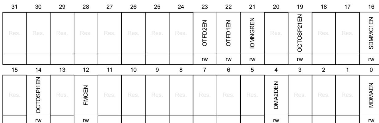
| 31 | 30 | 29 | 28 | 27 | 26 | 25 | 24 | 23 | 22 | 21 | 20 | 19 | 18 | 17 | 16 |
| Res. | Res. | Res. | Res. | Res. | Res. | Res. | Res. | OTFD2EN | OTFD1EN | IOMNGREN | Res. | OCTOSPI2EN | Res. | Res. | SDMMC1EN |
| rw | rw | rw | rw | rw | |||||||||||
| 15 | 14 | 13 | 12 | 11 | 10 | 9 | 8 | 7 | 6 | 5 | 4 | 3 | 2 | 1 | 0 |
| Res. | OCTOSPI1EN | Res. | FMCEN | Res. | Res. | Res. | Res. | Res. | Res. | Res. | DMA2DEN | Res. | Res. | Res. | MDMAEN |
| rw | rw | rw | rw |
Bits 31:24 Reserved, must be kept at reset value.
Bit 23
OTFD2EN
: OTFDEC2 clock enable
Set and reset by software.
0: OTFDEC2 clock disabled (default after reset)
1: OTFDEC2 clock enabled
Bit 22
OTFD1EN
: OTFDEC1 clock enable
Set and reset by software.
0: OTFDEC1 clock disabled (default after reset)
1: OTFDEC1 clock enabled
Bit 21
IOMNGREN
: OCTOSPI I/O manager clock enable
Set and reset by software.
0: OCTOSPI I/O manager clock disabled (default after reset)
1: OCTOSPI I/O manager clock enabled
Bit 20 Reserved, must be kept at reset value.
Bit 19
OCTOSPI2EN
: OCTOSPI2 and OCTOSPI2 delay clock enable
Set and reset by software.
0: OCTOSPI2 and OCTOSPI2 delay clock disabled (default after reset)
1: OCTOSPI2 and OCTOSPI2 delay clock enabled
Bits 18:17 Reserved, must be kept at reset value.
Bit 16
SDMMC1EN
: SDMMC1 and SDMMC1 Delay Clock Enable
Set and reset by software.
0: SDMMC1 and SDMMC1 Delay clock disabled (default after reset)
1: SDMMC1 and SDMMC1 Delay clock enabled
Bit 15 Reserved, must be kept at reset value.
Bit 14 OCTOSPI1EN : OCTOSPI1 and OCTOSPI1 delay clock enable
Set and reset by software.
0: OCTOSPI1 and OCTOSPI1 delay clock disabled (default after reset)
1: OCTOSPI1 and OCTOSPI1 delay clock enabled
Bit 13 Reserved, must be kept at reset value.
Bit 12 FMCEN : FMC Peripheral Clocks Enable
Set and reset by software.
0: FMC peripheral clocks disabled (default after reset)
1: FMC peripheral clocks enabled
The peripheral clocks of the FMC are: the kernel clock selected by FMCSEL and provided to fmc_ker_ck input, and the rcc_hclk3 bus interface clock.
Bits 11:5 Reserved, must be kept at reset value.
Bit 4 DMA2DEN : DMA2D Peripheral Clock Enable
Set and reset by software.
0: DMA2D peripheral clock disabled (default after reset)
1: DMA2D peripheral clock enabled
Bits 3:1 Reserved, must be kept at reset value.
Bit 0 MDMAEN : MDMA Peripheral Clock Enable
Set and reset by software.
0: MDMA peripheral clock disabled (default after reset)
1: MDMA peripheral clock enabled
8.7.40 RCC AHB1 clock register (RCC_AHB1ENR)
This register can be accessed via two different offset address.
Table 63. RCC_AHB1ENR address offset and reset value
| Register Name | Address Offset | Reset Value |
|---|---|---|
| RCC_AHB1ENR | 0x0D8 | 0x0000 0000 |
| RCC_C1_AHB1ENR | 0x138 |
| 31 | 30 | 29 | 28 | 27 | 26 | 25 | 24 | 23 | 22 | 21 | 20 | 19 | 18 | 17 | 16 |
|---|---|---|---|---|---|---|---|---|---|---|---|---|---|---|---|
| Res. | Res. | Res. | Res. | Res. | USB1OTGHSULPIEN | USB1OTGHSEN | Res. | Res. | Res. | Res. | Res. | Res. | Res. | ETH1RXEN | ETH1TXEN |
| rw | rw | rw | rw | ||||||||||||
| 15 | 14 | 13 | 12 | 11 | 10 | 9 | 8 | 7 | 6 | 5 | 4 | 3 | 2 | 1 | 0 |
| ETH1MACEN | Res. | Res. | Res. | Res. | Res. | Res. | Res. | Res. | Res. | ADC12EN | Res. | Res. | Res. | DMA2EN | DMA1EN |
| rw | rw | rw | rw |
Bits 31:27 Reserved, must be kept at reset value.
Bit 26 USB1OTGHSULPIEN : USB_PHY1 Clocks Enable
Set and reset by software.
0: USB1ULPI PHY clocks disabled (default after reset)
1: USB1ULPI PHY clocks enabled
Bit 25 USB1OTGHSEN : USB1OTG (OTG_HS1) Peripheral Clocks Enable
Set and reset by software.
0: USB1OTG peripheral clocks disabled (default after reset)
1: USB1OTG peripheral clocks enabled
The peripheral clocks of the USB1OTG are: the kernel clock selected by USBSEL and the rcc_hclk1 bus interface clock.
Bits 24:18 Reserved, must be kept at reset value.
Bit 17 ETH1RXEN : Ethernet Reception Clock Enable
Set and reset by software.
0: Ethernet Reception clock disabled (default after reset)
1: Ethernet Reception clock enabled
Bit 16 ETH1TXEN : Ethernet Transmission Clock Enable
Set and reset by software.
0: Ethernet Transmission clock disabled (default after reset)
1: Ethernet Transmission clock enabled
Bit 15 ETH1MACEN : Ethernet MAC bus interface Clock Enable
Set and reset by software.
0: Ethernet MAC bus interface clock disabled (default after reset)
1: Ethernet MAC bus interface clock enabled
Bits 14:6 Reserved, must be kept at reset value.
Bit 5 ADC12EN : ADC1/2 Peripheral Clocks Enable
Set and reset by software.
0: ADC1 and 2 peripheral clocks disabled (default after reset)
1: ADC1 and 2 peripheral clocks enabled
The peripheral clocks of the ADC1 and 2 are: the kernel clock selected by ADCSEL and provided to
adc_ker_ck_input
, and the
rcc_hclk1
bus interface clock.
Bits 4:2 Reserved, must be kept at reset value.
Bit 1 DMA2EN : DMA2 Clock Enable
Set and reset by software.
0: DMA2 clock disabled (default after reset)
1: DMA2 clock enabled
Bit 0 DMA1EN : DMA1 Clock Enable
Set and reset by software.
0: DMA1 clock disabled (default after reset)
1: DMA1 clock enabled
8.7.41 RCC AHB2 clock register (RCC_AHB2ENR)
This register can be accessed via two different offset address.
Table 64. RCC_AHB2ENR address offset and reset value
| Register Name | Address Offset | Reset Value |
|---|---|---|
| RCC_AHB2ENR | 0x0DC | 0x0000 0000 |
| RCC_C1_AHB2ENR | 0x13C |
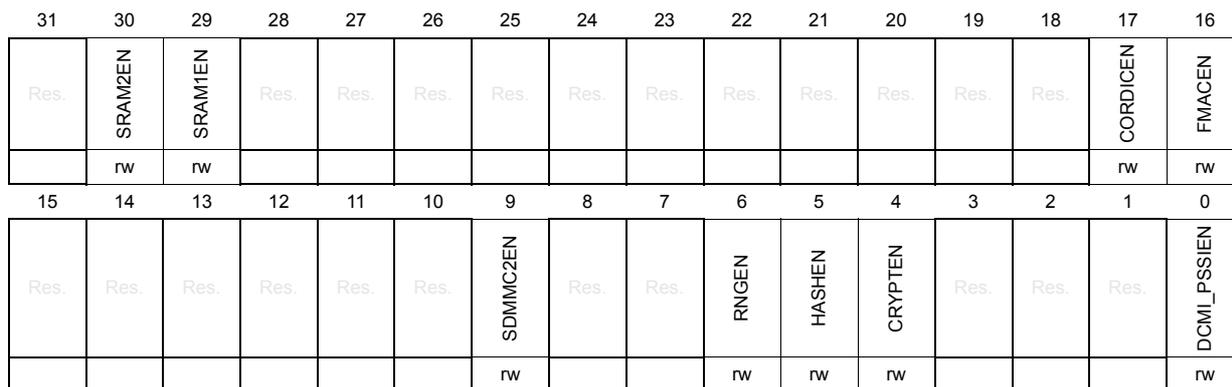
| 31 | 30 | 29 | 28 | 27 | 26 | 25 | 24 | 23 | 22 | 21 | 20 | 19 | 18 | 17 | 16 |
| Res. | SRAM2EN | SRAM1EN | Res. | Res. | Res. | Res. | Res. | Res. | Res. | Res. | Res. | Res. | Res. | CORDICEN | FMACEN |
| r/w | r/w | r/w | r/w |
| 15 | 14 | 13 | 12 | 11 | 10 | 9 | 8 | 7 | 6 | 5 | 4 | 3 | 2 | 1 | 0 |
| Res. | Res. | Res. | Res. | Res. | Res. | SDMMC2EN | Res. | Res. | RNGEN | HASHEN | CRYPTEN | Res. | Res. | Res. | DCML_PSS1EN |
| r/w | r/w | r/w | r/w | r/w |
Bit 31 Reserved, must be kept at reset value.
Bit 30 SRAM2EN : SRAM2 block enable
Set and reset by software.
When set, this bit indicates that the SRAM2 is allocated by the CPU. It causes the D2 domain to take into account also the CPU operation modes, i.e. keeping D2 domain in DRun when the CPU is in CRun.
0: SRAM2 interface clock is disabled. (default after reset)
1: SRAM2 interface clock is enabled.
Bit 29 SRAM1EN : SRAM1 block enable
Set and reset by software.
When set, this bit indicates that the SRAM1 is allocated by the CPU. It causes the D2 domain to take into account also the CPU operation modes, i.e. keeping D2 domain in DRun when the CPU is in CRun.
0: SRAM1 interface clock is disabled. (default after reset)
1: SRAM1 interface clock is enabled.
Bits 28:18 Reserved, must be kept at reset value.
Bit 17 CORDICEN : CORDIC peripheral clock enable
Set and reset by software.
0: CORDIC clock disabled (default after reset)
1: CORDIC clock enabled
Bit 16 FMACEN : FMAC peripheral clock enable
Set and reset by software.
0: FMAC clock disabled (default after reset)
1: FMAC clock enabled
Bits 15:10 Reserved, must be kept at reset value.
Bit 9 SDMMC2EN : SDMMC2 and SDMMC2 delay clock enable
Set and reset by software.
0: SDMMC2 and SDMMC2 Delay clock disabled (default after reset)
1: SDMMC2 and SDMMC2 Delay clock enabled
Bits 8:7 Reserved, must be kept at reset value.
Bit 6 RNGEN : RNG peripheral clocks enable
Set and reset by software.
0: RNG peripheral clocks disabled (default after reset)
1: RNG peripheral clocks enabled:
The peripheral clocks of the RNG are: the kernel clock selected by RNGSEL and provided to rng_ker_ck input, and the rcc_hclk2 bus interface clock.
Bit 5 HASHEN : HASH peripheral clock enable
Set and reset by software.
0: HASH peripheral clock disabled (default after reset)
1: HASH peripheral clock enabled
Bit 4 CRYPTEN : CRYPT peripheral clock enable
Set and reset by software.
0: CRYPT peripheral clock disabled (default after reset)
1: CRYPT peripheral clock enabled
Bits 3:1 Reserved, must be kept at reset value.
Bit 0 DCMI_PSSIEN : Digital camera interface clock enable (DCMI or PSSI, depending which peripheral is active)
Set and reset by software.
0: DCMI/PSSI peripheral clock disabled (default after reset)
1: DCMI/PSSI peripheral clock enabled
8.7.42 RCC AHB4 clock register (RCC_AHB4ENR)
This register can be accessed via two different offset address.
Table 65. RCC_AHB4ENR address offset and reset value
| Register Name | Address Offset | Reset Value |
|---|---|---|
| RCC_AHB4ENR | 0x0E0 | 0x0000 0000 |
| RCC_C1_AHB4ENR | 0x140 |
| 31 | 30 | 29 | 28 | 27 | 26 | 25 | 24 | 23 | 22 | 21 | 20 | 19 | 18 | 17 | 16 |
|---|---|---|---|---|---|---|---|---|---|---|---|---|---|---|---|
| Res. | Res. | Res. | BKPRAMEN | Res. | Res. | HSEMEN | ADC3EN | Res. | Res. | BDMAEN | Res. | CRCEN | Res. | Res. | Res. |
| rw | rw | rw | rw | rw | |||||||||||
| 15 | 14 | 13 | 12 | 11 | 10 | 9 | 8 | 7 | 6 | 5 | 4 | 3 | 2 | 1 | 0 |
| Res. | Res. | Res. | Res. | Res. | GPIOEN | GPIOJEN | Res. | GPIOHEN | GPIOGEN | GPIOFEN | GPIOEEN | GPIO DEN | GPIOCEN | GPIOBEN | GPIOAEN |
| rw | rw | rw | rw | rw | rw | rw | rw | rw | rw |
Bits 31:29 Reserved, must be kept at reset value.
Bit 28 BKPRAMEN : Backup RAM clock enable
Set and reset by software.
0: Backup RAM clock disabled (default after reset)
1: Backup RAM clock enabled
Bits 27:26 Reserved, must be kept at reset value.
Bit 25 HSEMEN : HSEM peripheral clock enable
Set and reset by software.
0: HSEM peripheral clock disabled (default after reset)
1: HSEM peripheral clock enabled
Bit 24 ADC3EN : ADC3 Peripheral Clocks Enable
Set and reset by software.
0: ADC3 peripheral clocks disabled (default after reset)
1: ADC3 peripheral clocks enabled
The peripheral clocks of the ADC3 are: the kernel clock selected by ADCSEL and provided to
adc_ker_ck_input
, and the
rcc_hclk4
bus interface clock.
Bits 23:22 Reserved, must be kept at reset value.
Bit 21 BDMAEN : BDMA and DMAMUX2 Clock Enable
Set and reset by software.
0: BDMA and DMAMUX2 clock disabled (default after reset)
1: BDMA and DMAMUX2 clock enabled
Bit 20 Reserved, must be kept at reset value.
Bit 19 CRCEN : CRC peripheral clock enable
Set and reset by software.
0: CRC peripheral clock disabled (default after reset)
1: CRC peripheral clock enabled
Bits 18:11 Reserved, must be kept at reset value.
Bit 10 GPIOEN : GPIO peripheral clock enable
Set and reset by software.
0: GPIO peripheral clock disabled (default after reset)
1: GPIO peripheral clock enabled
Bit 9 GPIOJEN : GPIOJ peripheral clock enable
Set and reset by software.
0: GPIOJ peripheral clock disabled (default after reset)
1: GPIOJ peripheral clock enabled
Bit 8 Reserved, must be kept at reset value.
Bit 7 GPIOHEN : GPIOH peripheral clock enable
Set and reset by software.
0: GPIOH peripheral clock disabled (default after reset)
1: GPIOH peripheral clock enabled
Bit 6 GPIOGEN : GPIOG peripheral clock enable
Set and reset by software.
0: GPIOG peripheral clock disabled (default after reset)
1: GPIOG peripheral clock enabled
Bit 5 GPIOFEN : GPIOF peripheral clock enable
Set and reset by software.
0: GPIOF peripheral clock disabled (default after reset)
1: GPIOF peripheral clock enabled
Bit 4 GPIOEEN : GPIOE peripheral clock enable
Set and reset by software.
0: GPIOE peripheral clock disabled (default after reset)
1: GPIOE peripheral clock enabled
Bit 3 GPIODEN : GPIOD peripheral clock enable
Set and reset by software.
0: GPIOD peripheral clock disabled (default after reset)
1: GPIOD peripheral clock enabled
Bit 2 GPIOCEN : GPIOC peripheral clock enable
Set and reset by software.
0: GPIOC peripheral clock disabled (default after reset)
1: GPIOC peripheral clock enabled
Bit 1 GPIOBEN : GPIOB peripheral clock enable
Set and reset by software.
0: GPIOB peripheral clock disabled (default after reset)
1: GPIOB peripheral clock enabled
Bit 0 GPIOAEN : GPIOA peripheral clock enable
Set and reset by software.
0: GPIOA peripheral clock disabled (default after reset)
1: GPIOA peripheral clock enabled
8.7.43 RCC APB3 clock register (RCC_APB3ENR)
This register can be accessed via two different offset address.
Table 66. RCC_APB3ENR address offset and reset value
| Register Name | Address Offset | Reset Value |
|---|---|---|
| RCC_APB3ENR | 0x0E4 | 0x0000 0000 |
| RCC_C1_APB3ENR | 0x144 |
| 31 | 30 | 29 | 28 | 27 | 26 | 25 | 24 | 23 | 22 | 21 | 20 | 19 | 18 | 17 | 16 |
|---|---|---|---|---|---|---|---|---|---|---|---|---|---|---|---|
| Res. | Res. | Res. | Res. | Res. | Res. | Res. | Res. | Res. | Res. | Res. | Res. | Res. | Res. | Res. | Res. |
| 15 | 14 | 13 | 12 | 11 | 10 | 9 | 8 | 7 | 6 | 5 | 4 | 3 | 2 | 1 | 0 |
| Res. | Res. | Res. | Res. | Res. | Res. | Res. | Res. | Res. | WWDG1EN | Res. | Res. | LTDCEN | Res. | Res. | Res. |
| rs | rw |
Bits 31:7 Reserved, must be kept at reset value.
Bit 6 WWDG1EN : WWDG1 Clock Enable
Set by software, and reset by hardware when a system reset occurs.
Note that in order to work properly, before enabling the WWDG1, the bit WW1RSC must be set to 1.
0: WWDG1 peripheral clock disable (default after reset)
1: WWDG1 peripheral clock enabled
Bits 5:4 Reserved, must be kept at reset value.
Bit 3 LTDCEN : LTDC peripheral clock enable
Provides the pixel clock ( ltcd_ker_ck ) to the LTDC block.
Set and reset by software.
0: LTDC peripheral clock disabled (default after reset)
1: LTDC peripheral clock provided to the LTDC block
Bits 2:0 Reserved, must be kept at reset value.
8.7.44 RCC APB1 clock register (RCC_APB1LENR)
This register can be accessed via two different offset address.
Table 67. RCC_APB1ENR address offset and reset value
| Register Name | Address Offset | Reset Value |
|---|---|---|
| RCC_APB1LENR | 0x0E8 | 0x0000 0000 |
| RCC_C1_APB1LENR | 0x148 |
| 31 | 30 | 29 | 28 | 27 | 26 | 25 | 24 | 23 | 22 | 21 | 20 | 19 | 18 | 17 | 16 |
|---|---|---|---|---|---|---|---|---|---|---|---|---|---|---|---|
| UART8EN | UART7EN | DAC12EN | Res. | CECEN | Res. | I2C5EN | Res. | I2C3EN | I2C2EN | I2C1EN | UART5EN | UART4EN | USART3EN | USART2EN | SPDIFRXEN |
| rw | rw | rw | rw | rw | rw | rw | rw | rw | rw | rw | rw | rw | |||
| 15 | 14 | 13 | 12 | 11 | 10 | 9 | 8 | 7 | 6 | 5 | 4 | 3 | 2 | 1 | 0 |
| SPI3EN | SPI2EN | Res. | Res. | Res. | Res. | LPTIM1EN | TIM14EN | TIM13EN | TIM12EN | TIM7EN | TIM6EN | TIM5EN | TIM4EN | TIM3EN | TIM2EN |
| rw | rw | rw | rw | rw | rw | rw | rw | rw | rw | rw | rw |
Bit 31 UART8EN: UART8 Peripheral Clocks Enable
Set and reset by software.
0: UART8 peripheral clocks disable (default after reset)
1: UART8 peripheral clocks enabled
The peripheral clocks of the UART8 are: the kernel clock selected by USART234578SEL and provided to usart_ker_ck input, and the rcc_pclk1 bus interface clock.
Bit 30 UART7EN: UART7 Peripheral Clocks Enable
Set and reset by software.
0: UART7 peripheral clocks disable (default after reset)
1: UART7 peripheral clocks enabled
The peripheral clocks of the UART7 are: the kernel clock selected by USART234578SEL and provided to usart_ker_ck input, and the rcc_pclk1 bus interface clock.
Bit 29 DAC12EN: DAC1 and 2 peripheral clock enable
Set and reset by software.
0: DAC1 and 2 peripheral clock disable (default after reset)
1: DAC1 and 2 peripheral clock enabled
Bit 28 Reserved, must be kept at reset value.
Bit 27 CECEN: HDMI-CEC peripheral clock enable
Set and reset by software.
0: HDMI-CEC peripheral clock disable (default after reset)
1: HDMI-CEC peripheral clock enabled
The peripheral clocks of the HDMI-CEC are: the kernel clock selected by CECSEL and provided to cec_ker_ck input, and the rcc_pclk1 bus interface clock.
Bits 26 Reserved, must be kept at reset value.
Bit 25 I2C5EN : I2C5 peripheral clocks enable
Set and reset by software.
0: I2C5 peripheral clocks disable (default after reset)
1: I2C5 peripheral clocks enabled
The peripheral clocks of the I2C5 are: the kernel clock selected by I2C1235SEL and provided to i2c_ker_ck input, and the rcc_pclk1 bus interface clock.
Bits 24 Reserved, must be kept at reset value.
Bit 23 I2C3EN : I2C3 peripheral clocks enable
Set and reset by software.
0: I2C3 peripheral clocks disable (default after reset)
1: I2C3 peripheral clocks enabled
The peripheral clocks of the I2C3 are: the kernel clock selected by I2C1235SEL and provided to i2c_ker_ck input, and the rcc_pclk1 bus interface clock.
Bit 22 I2C2EN : I2C2 Peripheral Clocks Enable
Set and reset by software.
0: I2C2 peripheral clocks disable (default after reset)
1: I2C2 peripheral clocks enabled
The peripheral clocks of the I2C2 are: the kernel clock selected by I2C1235SEL and provided to i2c_ker_ck input, and the rcc_pclk1 bus interface clock.
Bit 21 I2C1EN : I2C1 Peripheral Clocks Enable
Set and reset by software.
0: I2C1 peripheral clocks disable (default after reset)
1: I2C1 peripheral clocks enabled
The peripheral clocks of the I2C1 are: the kernel clock selected by I2C1235SEL and provided to i2c_ker_ck input, and the rcc_pclk1 bus interface clock.
Bit 20 UART5EN : UART5 Peripheral Clocks Enable
Set and reset by software.
0: UART5 peripheral clocks disable (default after reset)
1: UART5 peripheral clocks enabled
The peripheral clocks of the UART5 are: the kernel clock selected by USART234578SEL and provided to uart_ker_ck input, and the rcc_pclk1 bus interface clock.
Bit 19 UART4EN : UART4 Peripheral Clocks Enable
Set and reset by software.
0: UART4 peripheral clocks disable (default after reset)
1: UART4 peripheral clocks enabled
The peripheral clocks of the UART4 are: the kernel clock selected by USART234578SEL and provided to uart_ker_ck input, and the rcc_pclk1 bus interface clock.
Bit 18 USART3EN : USART3 Peripheral Clocks Enable
Set and reset by software.
0: USART3 peripheral clocks disable (default after reset)
1: USART3 peripheral clocks enabled
The peripheral clocks of the USART3 are: the kernel clock selected by USART234578SEL and provided to usart_ker_ck input, and the rcc_pclk1 bus interface clock.
Bit 17 USART2EN : USART2 Peripheral Clocks EnableSet and reset by software.
0: USART2 peripheral clocks disable (default after reset)
1: USART2 peripheral clocks enabled
The peripheral clocks of the USART2 are: the kernel clock selected by USART234578SEL and provided to usart_ker_ck input, and the rcc_pclk1 bus interface clock.
Bit 16 SPDIFRXEN : SPDIFRX Peripheral Clocks EnableSet and reset by software.
0: SPDIFRX peripheral clocks disable (default after reset)
1: SPDIFRX peripheral clocks enabled
The peripheral clocks of the SPDIFRX are: the kernel clock selected by SPDIFRXSEL and provided to spdifrx_ker_ck input, and the rcc_pclk1 bus interface clock.
Bit 15 SPI3EN : SPI3 Peripheral Clocks EnableSet and reset by software.
0: SPI3 peripheral clocks disable (default after reset)
1: SPI3 peripheral clocks enabled
The peripheral clocks of the SPI3 are: the kernel clock selected by I2S123SRC and provided to spi_ker_ck input, and the rcc_pclk1 bus interface clock.
Bit 14 SPI2EN : SPI2 Peripheral Clocks EnableSet and reset by software.
0: SPI2 peripheral clocks disable (default after reset)
1: SPI2 peripheral clocks enabled
The peripheral clocks of the SPI2 are: the kernel clock selected by I2S123SRC and provided to spi_ker_ck input, and the rcc_pclk1 bus interface clock.
Bits 13:10 Reserved, must be kept at reset value.
Bit 9 LPTIM1EN : LPTIM1 Peripheral Clocks EnableSet and reset by software.
0: LPTIM1 peripheral clocks disable (default after reset)
1: LPTIM1 peripheral clocks enabled
The peripheral clocks of the LPTIM1 are: the kernel clock selected by LPTIM1SEL and provided to lptim_ker_ck input, and the rcc_pclk1 bus interface clock.
Bit 8 TIM14EN : TIM14 peripheral clock enableSet and reset by software.
0: TIM14 peripheral clock disable (default after reset)
1: TIM14 peripheral clock enabled
Bit 7 TIM13EN : TIM13 peripheral clock enableSet and reset by software.
0: TIM13 peripheral clock disable (default after reset)
1: TIM13 peripheral clock enabled
Bit 6 TIM12EN : TIM12 peripheral clock enableSet and reset by software.
0: TIM12 peripheral clock disable (default after reset)
1: TIM12 peripheral clock enabled
Bit 5 TIM7EN : TIM7 peripheral clock enableSet and reset by software.
0: TIM7 peripheral clock disable (default after reset)
1: TIM7 peripheral clock enabled
- Bit 4
TIM6EN
: TIM6 peripheral clock enable
Set and reset by software.
0: TIM6 peripheral clock disable (default after reset)
1: TIM6 peripheral clock enabled - Bit 3
TIM5EN
: TIM5 peripheral clock enable
Set and reset by software.
0: TIM5 peripheral clock disable (default after reset)
1: TIM5 peripheral clock enabled - Bit 2
TIM4EN
: TIM4 peripheral clock enable
Set and reset by software.
0: TIM4 peripheral clock disable (default after reset)
1: TIM4 peripheral clock enabled - Bit 1
TIM3EN
: TIM3 peripheral clock enable
Set and reset by software.
0: TIM3 peripheral clock disable (default after reset)
1: TIM3 peripheral clock enabled - Bit 0
TIM2EN
: TIM2 peripheral clock enable
Set and reset by software.
0: TIM2 peripheral clock disable (default after reset)
1: TIM2 peripheral clock enabled
8.7.45 RCC APB1 clock register (RCC_APB1HENR)
This register can be accessed via two different offset address.
Table 68. RCC_APB1ENR address offset and reset value
| Register Name | Address Offset | Reset Value |
|---|---|---|
| RCC_APB1HENR | 0x0EC | 0x0000 0000 |
| RCC_C1_APB1HENR | 0x14C |
| 31 | 30 | 29 | 28 | 27 | 26 | 25 | 24 | 23 | 22 | 21 | 20 | 19 | 18 | 17 | 16 |
|---|---|---|---|---|---|---|---|---|---|---|---|---|---|---|---|
| Res. | Res. | Res. | Res. | Res. | Res. | TIM24EN | TIM23EN | Res. | Res. | Res. | Res. | Res. | Res. | Res. | Res. |
| rw | rw | ||||||||||||||
| 15 | 14 | 13 | 12 | 11 | 10 | 9 | 8 | 7 | 6 | 5 | 4 | 3 | 2 | 1 | 0 |
| Res. | Res. | Res. | Res. | Res. | Res. | Res. | FDCANEN | Res. | Res. | MDIOSEN | OPAMPEN | Res. | SWPMIEN | CRSEN | Res. |
| rw | rw | rw | rw | rw |
Bits 31:26 Reserved, must be kept at reset value.
Bit 25 TIM24EN : TIM24 peripheral clocks enable
Set and reset by software.
0: TIM24 peripheral clocks disable (default after reset)
1: TIM24 peripheral clocks enabled:
Bit 24 TIM23EN : TIM23 peripheral clocks enable
Set and reset by software.
0: TIM23 peripheral clocks disable (default after reset)
1: TIM23 peripheral clocks enabled:
Bits 23:9 Reserved, must be kept at reset value.
Bit 8 FDCANEN : FDCAN Peripheral Clocks Enable
Set and reset by software.
0: FDCAN peripheral clocks disable (default after reset)
1: FDCAN peripheral clocks enabled:
The peripheral clocks of the FDCAN are: the kernel clock selected by FDCANSEL and provided to fdcan_ker_ck input, and the rcc_pclk1 bus interface clock.
Bits 7:6 Reserved, must be kept at reset value.
Bit 5 MDIOSEN : MDIOS peripheral clock enable
Set and reset by software.
0: MDIOS peripheral clock disable (default after reset)
1: MDIOS peripheral clock enabled
Bit 4 OPAMPEN : OPAMP peripheral clock enable
Set and reset by software.
0: OPAMP peripheral clock disable (default after reset)
1: OPAMP peripheral clock enabled
Bit 3 Reserved, must be kept at reset value.
Bit 2 SWPMIEN: SWPMI Peripheral Clocks EnableSet and reset by software.
0: SWPMI peripheral clocks disable (default after reset)
1: SWPMI peripheral clocks enabled:
The peripheral clocks of the SWPMI are: the kernel clock selected by SWPMISEL and provided to swpmi_ker_ck input, and the rcc_pclk1 bus interface clock.
Bit 1 CRSEN: Clock Recovery System peripheral clock enableSet and reset by software.
0: CRS peripheral clock disable (default after reset)
1: CRS peripheral clock enabled
Bit 0 Reserved, must be kept at reset value.
8.7.46 RCC APB2 clock register (RCC_APB2ENR)
This register can be accessed via two different offset address.
Table 69. RCC_APB2ENR address offset and reset value
| Register Name | Address Offset | Reset Value |
|---|---|---|
| RCC_APB2ENR | 0x0F0 | 0x0000 0000 |
| RCC_C1_APB2ENR | 0x150 |
| 31 | 30 | 29 | 28 | 27 | 26 | 25 | 24 | 23 | 22 | 21 | 20 | 19 | 18 | 17 | 16 |
|---|---|---|---|---|---|---|---|---|---|---|---|---|---|---|---|
| Res. | DFSDM1EN | Res. | Res. | Res. | Res. | Res. | Res. | Res. | SAI1EN | Res. | SPI5EN | Res. | TIM17EN | TIM16EN | TIM15EN |
| rw | rw | rw | rw | rw | rw | ||||||||||
| 15 | 14 | 13 | 12 | 11 | 10 | 9 | 8 | 7 | 6 | 5 | 4 | 3 | 2 | 1 | 0 |
| Res. | Res. | SPI4EN | SPI1EN | Res. | Res. | Res. | Res. | USART10EN | UART9EN | USART6EN | USART1EN | Res. | Res. | TIM8EN | TIM1EN |
| rw | rw | rw | rw | rw | rw | rw | rw |
Bits 31 Reserved, must be kept at reset value.
Bit 30 DFSDM1EN : DFSDM1 Peripheral Clocks Enable
Set and reset by software.
0: DFSDM1 peripheral clocks disabled (default after reset)
1: DFSDM1 peripheral clocks enabled
DFSDM1 peripheral clocks are: the kernel clocks selected by SAI1SEL and DFSDM1SEL and provided to Aclk and clk inputs respectively, and the rcc_pclk2 bus interface clock.
Bits 29:23 Reserved, must be kept at reset value.
Bit 22 SAI1EN : SAI1 Peripheral Clocks Enable
Set and reset by software.
0: SAI1 peripheral clocks disabled (default after reset)
1: SAI1 peripheral clocks enabled:
The peripheral clocks of the SAI1 are: the kernel clock selected by SAI1SEL and provided to sai_a_ker_ck and sai_b_ker_ck inputs, and the rcc_pclk2 bus interface clock.
Bit 21 Reserved, must be kept at reset value.
Bit 20 SPI5EN : SPI5 Peripheral Clocks Enable
Set and reset by software.
0: SPI5 peripheral clocks disabled (default after reset)
1: SPI5 peripheral clocks enabled:
The peripheral clocks of the SPI5 are: the kernel clock selected by SPI45SEL and provided to spi_ker_ck input, and the rcc_pclk2 bus interface clock.
Bit 19 Reserved, must be kept at reset value.
Bit 18 TIM17EN : TIM17 peripheral clock enable
Set and reset by software.
0: TIM17 peripheral clock disabled (default after reset)
1: TIM17 peripheral clock enabled
Bit 17 TIM16EN : TIM16 peripheral clock enable
Set and reset by software.
0: TIM16 peripheral clock disabled (default after reset)
1: TIM16 peripheral clock enabled
Bit 16 TIM15EN : TIM15 peripheral clock enable
Set and reset by software.
0: TIM15 peripheral clock disabled (default after reset)
1: TIM15 peripheral clock enabled
Bits 15:14 Reserved, must be kept at reset value.
Bit 13 SPI4EN : SPI4 Peripheral Clocks Enable
Set and reset by software.
0: SPI4 peripheral clocks disabled (default after reset)
1: SPI4 peripheral clocks enabled:
The peripheral clocks of the SPI4 are: the kernel clock selected by SPI45SEL and provided to spi_ker_ck input, and the rcc_pclk2 bus interface clock.
Bit 12 SPI1EN : SPI1 Peripheral Clocks Enable
Set and reset by software.
0: SPI1 peripheral clocks disabled (default after reset)
1: SPI1 peripheral clocks enabled:
The peripheral clocks of the SPI1 are: the kernel clock selected by I2S123SRC and provided to spi_ker_ck input, and the rcc_pclk2 bus interface clock.
Bits 11:8 Reserved, must be kept at reset value.
Bit 7 USART10EN : USART10 peripheral clocks enable
Set and reset by software.
0: USART10 peripheral clocks disabled (default after reset)
1: USART10 peripheral clocks enabled:
The peripheral clocks of the USART10 are: the kernel clock selected by USART16910SEL and provided to usart_ker_ck input, and the rcc_pclk2 bus interface clock.
Bit 6 UART9EN : UART9 peripheral clocks enable
Set and reset by software.
0: UART9 peripheral clocks disabled (default after reset)
1: UART9 peripheral clocks enabled:
The peripheral clocks of the USART9 are the kernel clock selected by USART16910SEL and provided to usart_ker_ck input, and the rcc_pclk2 bus interface clock.
Bit 5 USART6EN : USART6 Peripheral Clocks Enable
Set and reset by software.
0: USART6 peripheral clocks disabled (default after reset)
1: USART6 peripheral clocks enabled:
The peripheral clocks of the USART6 are: the kernel clock selected by USART16910SEL and provided to usart_ker_ck input, and the rcc_pclk2 bus interface clock.
Bit 4 USART1EN : USART1 Peripheral Clocks Enable
Set and reset by software.
0: USART1 peripheral clocks disabled (default after reset)
1: USART1 peripheral clocks enabled:
The peripheral clocks of the USART1 are: the kernel clock selected by USART16910SEL and provided to usart_ker_ck input, and the rcc_pclk2 bus interface clock.
Bits 3:2 Reserved, must be kept at reset value.
Bit 1 TIM8EN : TIM8 peripheral clock enable
Set and reset by software.
0: TIM8 peripheral clock disabled (default after reset)
1: TIM8 peripheral clock enabled
Bit 0 TIM1EN : TIM1 peripheral clock enable
Set and reset by software.
0: TIM1 peripheral clock disabled (default after reset)
1: TIM1 peripheral clock enabled
8.7.47 RCC APB4 clock register (RCC_APB4ENR)
This register can be accessed via two different offset address.
Table 70. RCC_APB4ENR address offset and reset value
| Register Name | Address Offset | Reset Value |
|---|---|---|
| RCC_APB4ENR | 0x0F4 | 0x0001 0000 |
| RCC_C1_APB4ENR | 0x154 |
| 31 | 30 | 29 | 28 | 27 | 26 | 25 | 24 | 23 | 22 | 21 | 20 | 19 | 18 | 17 | 16 |
|---|---|---|---|---|---|---|---|---|---|---|---|---|---|---|---|
| Res. | Res. | Res. | Res. | Res. | DTSEN | Res. | Res. | Res. | Res. | SAI4EN | Res. | Res. | Res. | Res. | RTCAPBEN |
| rw | rw | rw |
| 15 | 14 | 13 | 12 | 11 | 10 | 9 | 8 | 7 | 6 | 5 | 4 | 3 | 2 | 1 | 0 |
|---|---|---|---|---|---|---|---|---|---|---|---|---|---|---|---|
| VREFEN | COMP12EN | Res. | LPTIM5EN | LPTIM4EN | LPTIM3EN | LPTIM2EN | Res. | I2C4EN | Res. | SPI6EN | Res. | LPUART1EN | Res. | SYSCFGEN | Res. |
| rw | rw | rw | rw | rw | rw | rw | rw | rw | rw |
Bits 31:27 Reserved, must be kept at reset value.
Bit 26 DTSEN : Digital temperature sensor peripheral clock enable
Set and reset by software.
0: Digital temperature sensor peripheral clock disabled (default after reset)
1: Digital temperature sensor peripheral clock enabled
Bits 25:22 Reserved, must be kept at reset value.
Bit 21 SAI4EN : SAI4 Peripheral Clocks Enable
Set and reset by software.
0: SAI4 peripheral clocks disabled (default after reset)
1: SAI4 peripheral clocks enabled
The peripheral clocks of the SAI4 are: the kernel clocks selected by SAI4ASEL and SAI4BSEL, and provided to sai_a_ker_ck and sai_b_ker_ck inputs respectively, and the rcc_pclk4 bus interface clock.
Bits 20:17 Reserved, must be kept at reset value.
Bit 16 RTCAPBEN : RTC APB Clock Enable
Set and reset by software.
0: The register clock interface of the RTC (APB) is disabled
1: The register clock interface of the RTC (APB) is enabled (default after reset)
Bit 15 VREFEN : VREFBUF peripheral clock enable
Set and reset by software.
0: VREF peripheral clock disabled (default after reset)
1: VREF peripheral clock enabled
- Bit 14
COMP12EN
: COMP1/2 peripheral clock enable
Set and reset by software.
0: COMP1/2 peripheral clock disabled (default after reset)
1: COMP1/2 peripheral clock enabled - Bit 13 Reserved, must be kept at reset value.
- Bit 12
LPTIM5EN
: LPTIM5 Peripheral Clocks Enable
Set and reset by software.
0: LPTIM5 peripheral clocks disabled (default after reset)
1: LPTIM5 peripheral clocks enabled
The peripheral clocks of the LPTIM5 are: the kernel clock selected by LPTIM345SEL and provided to lptim_ker_ck input, and the rcc_pclk4 bus interface clock. - Bit 11
LPTIM4EN
: LPTIM4 Peripheral Clocks Enable
Set and reset by software.
0: LPTIM4 peripheral clocks disabled (default after reset)
1: LPTIM4 peripheral clocks enabled
The peripheral clocks of the LPTIM4 are: the kernel clock selected by LPTIM345SEL and provided to lptim_ker_ck input, and the rcc_pclk4 bus interface clock. - Bit 10
LPTIM3EN
: LPTIM3 Peripheral Clocks Enable
Set and reset by software.
0: LPTIM3 peripheral clocks disabled (default after reset)
1: LPTIM3 peripheral clocks enabled
The peripheral clocks of the LPTIM3 are: the kernel clock selected by LPTIM345SEL and provided to lptim_ker_ck input, and the rcc_pclk4 bus interface clock. - Bit 9
LPTIM2EN
: LPTIM2 Peripheral Clocks Enable
Set and reset by software.
0: LPTIM2 peripheral clocks disabled (default after reset)
1: LPTIM2 peripheral clocks enabled
The peripheral clocks of the LPTIM2 are: the kernel clock selected by LPTIM2SEL and provided to lptim_ker_ck input, and the rcc_pclk4 bus interface clock. - Bit 8 Reserved, must be kept at reset value.
- Bit 7
I2C4EN
: I2C4 Peripheral Clocks Enable
Set and reset by software.
0: I2C4 peripheral clocks disabled (default after reset)
1: I2C4 peripheral clocks enabled
The peripheral clocks of the I2C4 are: the kernel clock selected by I2C4SEL and provided to i2c_ker_ck input, and the rcc_pclk4 bus interface clock. - Bit 6 Reserved, must be kept at reset value.
- Bit 5
SPI6EN
: SPI6 Peripheral Clocks Enable
Set and reset by software.
0: SPI6 peripheral clocks disabled (default after reset)
1: SPI6 peripheral clocks enabled
The peripheral clocks of the SPI6 are: the kernel clock selected by SPI6SEL and provided to spi_ker_ck input, and the rcc_pclk4 bus interface clock. - Bit 4 Reserved, must be kept at reset value.
Bit 3 LPUART1EN : LPUART1 Peripheral Clocks Enable
Set and reset by software.
0: LPUART1 peripheral clocks disabled (default after reset)
1: LPUART1 peripheral clocks enabled
The peripheral clocks of the LPUART1 are: the kernel clock selected by LPUART1SEL and provided to lpuart_ker_ck input, and the rcc_pclk4 bus interface clock.
Bit 2 Reserved, must be kept at reset value.
Bit 1 SYSCFGEN : SYSCFG peripheral clock enable
Set and reset by software.
0: SYSCFG peripheral clock disabled (default after reset)
1: SYSCFG peripheral clock enabled
Bit 0 Reserved, must be kept at reset value.
8.7.48 RCC AHB3 Sleep clock register (RCC_AHB3LPENR)
This register can be accessed via two different offset address.
Table 71. RCC_AHB3LPENR address offset and reset value
| Register Name | Address Offset | Reset Value |
|---|---|---|
| RCC_AHB3LPENR | 0x0FC | 0xF0E9 5111 |
| RCC_C1_AHB3LPENR | 0x15C |
| 31 | 30 | 29 | 28 | 27 | 26 | 25 | 24 | 23 | 22 | 21 | 20 | 19 | 18 | 17 | 16 |
|---|---|---|---|---|---|---|---|---|---|---|---|---|---|---|---|
| AXISRAMLPEN | ITCMLPEN | DTOM2LPEN | DTOM1LPEN | Res. | Res. | Res. | Res. | OTFD2LPEN | OTFD1LPEN | IOMNGRLPEN | Res. | OCTO2LPEN | Res. | Res. | SDMMC1LPEN |
| r/w | r/w | r/w | r/w | r/w | r/w | r/w | r/w | r/w | |||||||
| 15 | 14 | 13 | 12 | 11 | 10 | 9 | 8 | 7 | 6 | 5 | 4 | 3 | 2 | 1 | 0 |
| Res. | OCTO1LPEN | Res. | FMCLPEN | Res. | Res. | Res. | FLASHLPEN | Res. | Res. | Res. | DMA2DLPEN | Res. | Res. | Res. | MDMALPEN |
| r/w | r/w | r/w | r/w | r/w |
Bit 31 AXISRAMLPEN : AXISRAM Block Clock Enable During CSleep mode
Set and reset by software.
0: AXISRAM interface clock disabled during CSleep mode
1: AXISRAM interface clock enabled during CSleep mode (default after reset)
Bit 30 ITCMLPEN : D1ITCM Block Clock Enable During CSleep mode
Set and reset by software.
0: D1 ITCM interface clock disabled during CSleep mode
1: D1 ITCM interface clock enabled during CSleep mode (default after reset)
Bit 29 DTOM2LPEN : D1 DTCM2 Block Clock Enable During CSleep mode
Set and reset by software.
0: D1 DTCM2 interface clock disabled during CSleep mode
1: D1 DTCM2 interface clock enabled during CSleep mode (default after reset)
Bit 28 D1DTCM1LPEN : D1DTCM1 Block Clock Enable During CSleep mode
Set and reset by software.
0: D1DTCM1 interface clock disabled during CSleep mode
1: D1DTCM1 interface clock enabled during CSleep mode (default after reset)
Bits 27:24 Reserved, must be kept at reset value.
Bit 23 OTFD2LPEN : OTFDEC2 clock enable during CSleep mode
Set and reset by software.
0: OTFDEC2 clock disabled during CSleep mode
1: OTFDEC2 clock enabled during CSleep mode (default after reset)
Bit 22 OTFD1LPEN : OTFDEC1 clock enable during CSleep mode
Set and reset by software.
0: OTFDEC1 clock disabled during CSleep mode
1: OTFDEC1 clock enabled during CSleep mode (default after reset)
Bit 21 IOMNGRLPEN : OCTOSPI I/O manager clock enable during CSleep mode
Set and reset by software.
0: OCTOSPI I/O manager clock disabled during CSleep mode
1: OCTOSPI I/O manager clock enabled during CSleep mode (default after reset)
Bit 20 Reserved, must be kept at reset value.
Bit 19 OCTO2LPEN : OCTOSPI2 clock enable during CSleep mode
Set and reset by software.
0: OCTOSPI2 clock disabled during CSleep mode
1: OCTOSPI2 clock enabled during CSleep mode (default after reset)
Bits 18:17 Reserved, must be kept at reset value.
Bit 16 SDMMC1LPEN : SDMMC1 and SDMMC1 Delay Clock Enable During CSleep Mode
Set and reset by software.
0: SDMMC1 and SDMMC1 Delay clock disabled during CSleep mode
1: SDMMC1 and SDMMC1 Delay clock enabled during CSleep mode (default after reset)
Bit 15 Reserved, must be kept at reset value.
Bit 14 OCTO1LPEN : OCTOSPI1 clock enable during CSleep mode
Set and reset by software.
0: OCTOSPI1 clock disabled during CSleep mode
1: OCTOSPI1 clock enabled during CSleep mode (default after reset)
Bit 13 Reserved, must be kept at reset value.
Bit 12 FMCLPEN : FMC Peripheral Clocks Enable During CSleep Mode
Set and reset by software.
0: FMC peripheral clocks disabled during CSleep mode
1: FMC peripheral clocks enabled during CSleep mode (default after reset):
The peripheral clocks of the FMC are: the kernel clock selected by FMCSEL and provided to fmc_ker_ck input, and the rcc_hclk3 bus interface clock.
Bits 11:9 Reserved, must be kept at reset value.
Bit 8 FLASHLPEN : Flash interface Clock Enable During CSleep Mode
Set and reset by software.
0: Flash interface clock disabled during CSleep mode
1: Flash interface clock enabled during CSleep mode (default after reset)
Bits 7:5 Reserved, must be kept at reset value.
Bit 4 DMA2DLPEN : DMA2D Clock Enable During CSleep Mode
Set and reset by software.
0: DMA2D peripheral clock disabled during CSleep mode
1: DMA2D peripheral clock enabled during CSleep mode (default after reset)
Bits 3:1 Reserved, must be kept at reset value.
Bit 0 MDMALPEN : MDMA Clock Enable During CSleep Mode
Set and reset by software.
0: MDMA peripheral clock disabled during CSleep mode
1: MDMA peripheral clock enabled during CSleep mode (default after reset)
8.7.49 RCC AHB1 Sleep clock register (RCC_AHB1LPENR)
This register can be accessed via two different offset address.
Table 72. RCC_AHB1LPENR address offset and reset value
| Register Name | Address Offset | Reset Value |
|---|---|---|
| RCC_AHB1LPENR | 0x100 | 0x0603 8023 |
| RCC_C1_AHB1LPENR | 0x160 |
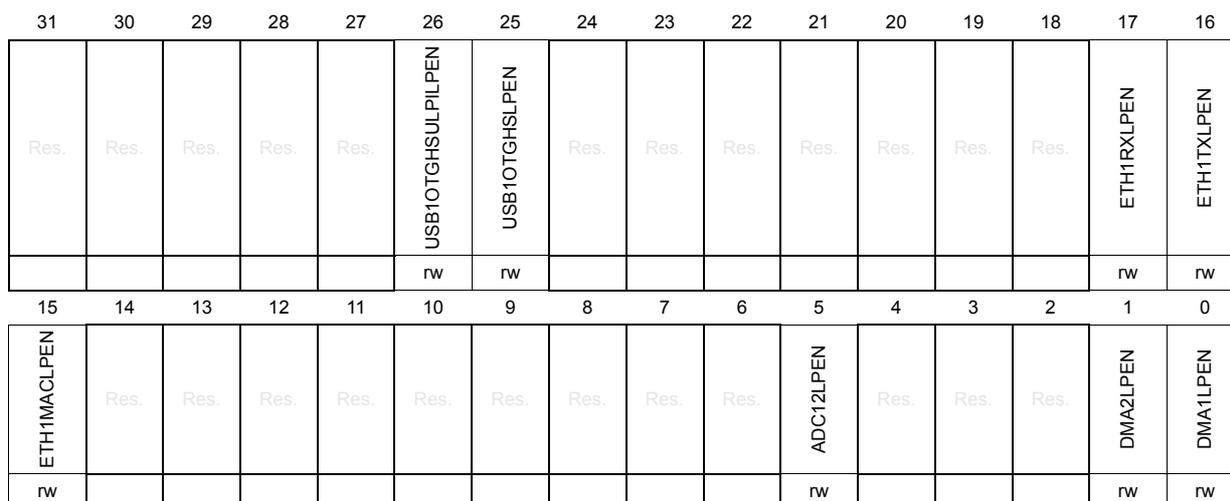
| 31 | 30 | 29 | 28 | 27 | 26 | 25 | 24 | 23 | 22 | 21 | 20 | 19 | 18 | 17 | 16 |
| Res. | Res. | Res. | Res. | Res. | USB1OTGHSULPILPEN | USB1OTGHSLOPEN | Res. | Res. | Res. | Res. | Res. | Res. | Res. | ETH1RXLPEN | ETH1TXLPEN |
| rw | rw | rw | rw | ||||||||||||
| 15 | 14 | 13 | 12 | 11 | 10 | 9 | 8 | 7 | 6 | 5 | 4 | 3 | 2 | 1 | 0 |
| ETH1MACLPEN | Res. | Res. | Res. | Res. | Res. | Res. | Res. | Res. | Res. | ADC12LPEN | Res. | Res. | Res. | DMA2LPEN | DMA1LPEN |
| rw | rw | rw | rw |
Bits 31:27 Reserved, must be kept at reset value.
Bit 26 USB1OTGHSULPILPEN : USB_PHY1 clock enable during CSleep mode
Set and reset by software.
- 0: USB_PHY1 peripheral clock disabled during CSleep mode
- 1: USB_PHY1 peripheral clock enabled during CSleep mode (default after reset)
Bit 25 USB1OTGHSLOPEN : USB1OTG (OTG_HS1) peripheral clock enable during CSleep mode
Set and reset by software.
- 0: USB1OTG peripheral clock disabled during CSleep mode
- 1: USB1OTG peripheral clock enabled during CSleep mode (default after reset)
The peripheral clocks of the USB1OTG are: the kernel clock selected by USBSEL and the rcc_hclk1 bus interface clock.
Bits 24:18 Reserved, must be kept at reset value.
Bit 17 ETH1RXLPEN : Ethernet Reception Clock Enable During CSleep Mode
Set and reset by software.
- 0: Ethernet Reception clock disabled during CSleep mode
- 1: Ethernet Reception clock enabled during CSleep mode (default after reset)
Bit 16 ETH1TXLPEN : Ethernet Transmission Clock Enable During CSleep Mode
Set and reset by software.
- 0: Ethernet Transmission clock disabled during CSleep mode
- 1: Ethernet Transmission clock enabled during CSleep mode (default after reset)
Bit 15 ETH1MACLPEN : Ethernet MAC bus interface Clock Enable During CSleep Mode
Set and reset by software.
0: Ethernet MAC bus interface clock disabled during CSleep mode
1: Ethernet MAC bus interface clock enabled during CSleep mode (default after reset)
Bits 14:6 Reserved, must be kept at reset value.
Bit 5 ADC12LPEN : ADC1/2 Peripheral Clocks Enable During CSleep Mode
Set and reset by software.
0: ADC1/2 peripheral clocks disabled during CSleep mode
1: ADC1/2 peripheral clocks enabled during CSleep mode (default after reset)
The peripheral clocks of the ADC1 and 2 are: the kernel clock selected by ADCSEL and provided to
adc_ker_ck_input
, and the
rcc_hclk1
bus interface clock.
Bits 4:2 Reserved, must be kept at reset value.
Bit 1 DMA2LPEN : DMA2 Clock Enable During CSleep Mode
Set and reset by software.
0: DMA2 clock disabled during CSleep mode
1: DMA2 clock enabled during CSleep mode (default after reset)
Bit 0 DMA1LPEN : DMA1 Clock Enable During CSleep Mode
Set and reset by software.
0: DMA1 clock disabled during CSleep mode
1: DMA1 clock enabled during CSleep mode (default after reset)
8.7.50 RCC AHB2 Sleep clock register (RCC_AHB2LPENR)
This register can be accessed via two different offset address.
Table 73. RCC_AHB2LPENR address offset and reset value
| Register Name | Address Offset | Reset Value |
|---|---|---|
| RCC_AHB2LPENR | 0x104 | 0x6003 0271 |
| RCC_C1_AHB2LPENR | 0x164 |
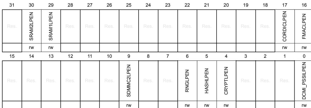
| 31 | 30 | 29 | 28 | 27 | 26 | 25 | 24 | 23 | 22 | 21 | 20 | 19 | 18 | 17 | 16 |
| Res. | SRAM2LPEN | SRAM1LPEN | Res. | Res. | Res. | Res. | Res. | Res. | Res. | Res. | Res. | Res. | Res. | CORDICLPEN | FMACLPEN |
| rw | rw | rw | rw |
| 15 | 14 | 13 | 12 | 11 | 10 | 9 | 8 | 7 | 6 | 5 | 4 | 3 | 2 | 1 | 0 |
| Res. | Res. | Res. | Res. | Res. | Res. | SDMMC2LPEN | Res. | Res. | RNGLPEN | HASHLPEN | CRYPTLPEN | Res. | Res. | Res. | DCMI_PSSILPEN |
| rw | rw | rw | rw | rw |
Bit 31 Reserved, must be kept at reset value.
Bit 30 SRAM2LPEN : SRAM2 Clock Enable During CSleep Mode
Set and reset by software.
0: SRAM2 clock disabled during CSleep mode
1: SRAM2 clock enabled during CSleep mode (default after reset)
Bit 29 SRAM1LPEN : SRAM1 Clock Enable During CSleep Mode
Set and reset by software.
0: SRAM1 clock disabled during CSleep mode
1: SRAM1 clock enabled during CSleep mode (default after reset)
Bits 28:18 Reserved, must be kept at reset value.
Bit 17 CORDICLPEN : CORDIC clock enable during CSleep mode
Set and reset by software.
0: CORDIC clock disabled during CSleep mode
1: CORDIC clock enabled during CSleep mode (default after reset)
Bit 16 FMACLPEN : FMAC clock enable during CSleep mode
Set and reset by software.
0: FMAC clock disabled during CSleep mode
1: FMAC clock enabled during CSleep mode (default after reset)
Bits 15:10 Reserved, must be kept at reset value.
Bit 9 SDMMC2LPEN : SDMMC2 and SDMMC2 Delay Clock Enable During CSleep Mode
Set and reset by software.
0: SDMMC2 and SDMMC2 Delay clock disabled during CSleep mode
1: SDMMC2 and SDMMC2 Delay clock enabled during CSleep mode (default after reset)
Bits 8:7 Reserved, must be kept at reset value.
Bit 6 RNGLPEN : RNG peripheral clock enable during CSleep mode
Set and reset by software.
0: RNG peripheral clocks disabled during CSleep mode
1: RNG peripheral clock enabled during CSleep mode (default after reset)
The peripheral clocks of the RNG are: the kernel clock selected by RNGSEL and provided to rng_ker_ck input, and the rcc_hclk2 bus interface clock.
Bit 5 HASHPEN : HASH peripheral clock enable during CSleep mode
Set and reset by software.
0: HASH peripheral clock disabled during CSleep mode
1: HASH peripheral clock enabled during CSleep mode (default after reset)
Bit 4 CRYPTLPEN : CRYPT peripheral clock enable during CSleep mode
Set and reset by software.
0: CRYPT peripheral clock disabled during CSleep mode
1: CRYPT peripheral clock enabled during CSleep mode (default after reset)
Bits 3:1 Reserved, must be kept at reset value.
Bit 0 DCMI_PSSILPEN : Digital camera interface clock enable during CSleep mode (DCMI or PSSI depending which peripheral is active)
Set and reset by software.
0: DCMI/PSSI peripheral clock disabled during CSleep mode
1: DCMI/PSSI peripheral clock enabled during CSleep mode (default after reset)
8.7.51 RCC AHB4 Sleep clock register (RCC_AHB4LPENR)
This register can be accessed via two different offset address.
Table 74. RCC_AHB4LPENR address offset and reset value
| Register Name | Address Offset | Reset Value |
|---|---|---|
| RCC_AHB4LPENR | 0x108 | 0x3128 06FF |
| RCC_C1_AHB4LPENR | 0x168 |
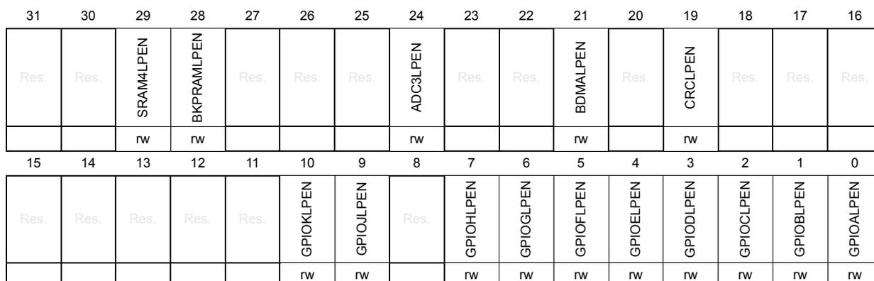
| 31 | 30 | 29 | 28 | 27 | 26 | 25 | 24 | 23 | 22 | 21 | 20 | 19 | 18 | 17 | 16 |
| Res. | Res. | SRAM4LPEN | BKPRAMLPEN | Res. | Res. | Res. | ADC3LPEN | Res. | Res. | BDMALPEN | Res. | CROLPEN | Res. | Res. | Res. |
| rw | rw | rw | rw | rw | |||||||||||
| 15 | 14 | 13 | 12 | 11 | 10 | 9 | 8 | 7 | 6 | 5 | 4 | 3 | 2 | 1 | 0 |
| Res. | Res. | Res. | Res. | Res. | GPIOKLPEN | GPIOJLPEN | Res. | GPIOHLPEN | GPIOGLPEN | GPIOFLPEN | GPIOELPEN | GPIOILPEN | GPIOCLPEN | GPIOBLPEN | GPIOALPEN |
| rw | rw | rw | rw | rw | rw | rw | rw | rw | rw |
Bits 31:30 Reserved, must be kept at reset value.
Bit 29 SRAM4LPEN : SRAM4 Clock Enable During CSleep Mode
Set and reset by software.
0: SRAM4 clock disabled during CSleep mode
1: SRAM4 clock enabled during CSleep mode (default after reset)
Bit 28 BKPRAMLPEN : Backup RAM Clock Enable During CSleep Mode
Set and reset by software.
0: Backup RAM clock disabled during CSleep mode
1: Backup RAM clock enabled during CSleep mode (default after reset)
Bits 27:25 Reserved, must be kept at reset value.
Bit 24 ADC3LPEN : ADC3 Peripheral Clocks Enable During CSleep Mode
Set and reset by software.
0: ADC3 peripheral clocks disabled during CSleep mode
1: ADC3 peripheral clocks enabled during CSleep mode (default after reset)
The peripheral clocks of the ADC3 are: the kernel clock selected by ADCSEL and provided to
adc_ker_ck_input
, and the
rcc_hclk4
bus interface clock.
Bits 23:22 Reserved, must be kept at reset value.
Bit 21 BDMALPEN : BDMA Clock Enable During CSleep Mode
Set and reset by software.
0: BDMA clock disabled during CSleep mode
1: BDMA clock enabled during CSleep mode (default after reset)
Bit 20 Reserved, must be kept at reset value.
Bit 19 CRCLPEN : CRC peripheral clock enable during CSleep mode
Set and reset by software.
0: CRC peripheral clock disabled during CSleep mode
1: CRC peripheral clock enabled during CSleep mode (default after reset)
Bits 18:11 Reserved, must be kept at reset value.
Bit 10 GPIOKLPEN : GPIOK peripheral clock enable during CSleep mode
Set and reset by software.
0: GPIOK peripheral clock disabled during CSleep mode
1: GPIOK peripheral clock enabled during CSleep mode (default after reset)
Bit 9 GPIOJLPEN : GPIOJ peripheral clock enable during CSleep mode
Set and reset by software.
0: GPIOJ peripheral clock disabled during CSleep mode
1: GPIOJ peripheral clock enabled during CSleep mode (default after reset)
Bit 8 Reserved, must be kept at reset value.
Bit 7 GPIOHLPEN : GPIOH peripheral clock enable during CSleep mode
Set and reset by software.
0: GPIOH peripheral clock disabled during CSleep mode
1: GPIOH peripheral clock enabled during CSleep mode (default after reset)
Bit 6 GPIOGLPEN : GPIOG peripheral clock enable during CSleep mode
Set and reset by software.
0: GPIOG peripheral clock disabled during CSleep mode
1: GPIOG peripheral clock enabled during CSleep mode (default after reset)
Bit 5 GPIOFLPEN : GPIOF peripheral clock enable during CSleep mode
Set and reset by software.
0: GPIOF peripheral clock disabled during CSleep mode
1: GPIOF peripheral clock enabled during CSleep mode (default after reset)
Bit 4 GPIOELPEN : GPIOE peripheral clock enable during CSleep mode
Set and reset by software.
0: GPIOE peripheral clock disabled during CSleep mode
1: GPIOE peripheral clock enabled during CSleep mode (default after reset)
Bit 3 GPIODLPEN : GPIOD peripheral clock enable during CSleep mode
Set and reset by software.
0: GPIOD peripheral clock disabled during CSleep mode
1: GPIOD peripheral clock enabled during CSleep mode (default after reset)
Bit 2 GPIOCLPEN : GPIOC peripheral clock enable during CSleep mode
Set and reset by software.
0: GPIOC peripheral clock disabled during CSleep mode
1: GPIOC peripheral clock enabled during CSleep mode (default after reset)
Bit 1 GPIOBLPEN : GPIOB peripheral clock enable during CSleep mode
Set and reset by software.
0: GPIOB peripheral clock disabled during CSleep mode
1: GPIOB peripheral clock enabled during CSleep mode (default after reset)
Bit 0 GPIOALPEN : GPIOA peripheral clock enable during CSleep mode
Set and reset by software.
0: GPIOA peripheral clock disabled during CSleep mode
1: GPIOA peripheral clock enabled during CSleep mode (default after reset)
8.7.52 RCC APB3 Sleep Clock Register (RCC_APB3LPENR)
This register can be accessed via two different offset address.
Table 75. RCC_APB3LPENR address offset and reset value
| Register Name | Address Offset | Reset Value |
|---|---|---|
| RCC_APB3LPENR | 0x10C | 0x0000 0048 |
| RCC_C1_APB3LPENR | 0x16C |
| 31 | 30 | 29 | 28 | 27 | 26 | 25 | 24 | 23 | 22 | 21 | 20 | 19 | 18 | 17 | 16 |
|---|---|---|---|---|---|---|---|---|---|---|---|---|---|---|---|
| Res. | Res. | Res. | Res. | Res. | Res. | Res. | Res. | Res. | Res. | Res. | Res. | Res. | Res. | Res. | Res. |
| 15 | 14 | 13 | 12 | 11 | 10 | 9 | 8 | 7 | 6 | 5 | 4 | 3 | 2 | 1 | 0 |
| Res. | Res. | Res. | Res. | Res. | Res. | Res. | Res. | Res. | WWDG1LPEN | Res. | Res. | LTDC1LPEN | Res. | Res. | Res. |
| r/w | r/w |
Bits 31:7 Reserved, must be kept at reset value.
Bit 6 WWDG1LPEN : WWDG1 Clock Enable During CSleep Mode
Set and reset by software.
0: WWDG1 clock disable during CSleep mode
1: WWDG1 clock enabled during CSleep mode (default after reset)
Bits 5:4 Reserved, must be kept at reset value.
Bit 3 LTDC1LPEN : LTDC peripheral clock enable during CSleep mode
Provides the pixel clock ( ltdc_ker_ck ) to the LTDC block.
Set and reset by software.
0: LTDC clock disabled during CSleep mode
1: LTDC clock provided to the LTDC during CSleep mode (default after reset)
Bits 2:0 Reserved, must be kept at reset value.
8.7.53 RCC APB1 Low Sleep clock register (RCC_APB1LLPENR)
This register can be accessed via two different offset address.
Table 76. RCC_APB1LLPENR address offset and reset value
| Register Name | Address Offset | Reset Value |
|---|---|---|
| RCC_APB1LLPENR | 0x110 | 0xEA9FF C3FF |
| RCC_C1_APB1LLPENR | 0x170 |
| 31 | 30 | 29 | 28 | 27 | 26 | 25 | 24 | 23 | 22 | 21 | 20 | 19 | 18 | 17 | 16 |
| UART8LPEN | UART7LPEN | DAC12LPEN | Res. | CECLPEN | Res. | I2C5LPEN | Res. | I2C3LPEN | I2C2LPEN | I2C1LPEN | UART5LPEN | UART4LPEN | USART3LPEN | USART2LPEN | SPDIFRXLPEN |
| r | r | r | r | r | r | r | r | r | r | r | r | r | |||
| 15 | 14 | 13 | 12 | 11 | 10 | 9 | 8 | 7 | 6 | 5 | 4 | 3 | 2 | 1 | 0 |
| SPI3LPEN | SPI2LPEN | Res. | Res. | Res. | Res. | LPTIM1LPEN | TIM14LPEN | TIM13LPEN | TIM12LPEN | TIM7LPEN | TIM6LPEN | TIM5LPEN | TIM4LPEN | TIM3LPEN | TIM2LPEN |
| r | r | r | r | r | r | r | r | r | r | r | r |
Bit 31 UART8LPEN : UART8 Peripheral Clocks Enable During CSleep Mode
Set and reset by software.
0: UART8 peripheral clocks disabled during CSleep mode
1: UART8 peripheral clocks enabled during CSleep mode (default after reset):
The peripheral clocks of the UART8 are: the kernel clock selected by USART234578SEL and provided to usart_ker_ck input, and the rcc_pclk1 bus interface clock.
Bit 30 UART7LPEN : UART7 Peripheral Clocks Enable During CSleep Mode
Set and reset by software.
0: UART7 peripheral clocks disabled during CSleep mode
1: UART7 peripheral clocks enabled during CSleep mode (default after reset):
The peripheral clocks of the UART7 are: the kernel clock selected by USART234578SEL and provided to usart_ker_ck input, and the rcc_pclk1 bus interface clock.
Bit 29 DAC12LPEN : DAC1/2 peripheral clock enable during CSleep mode
Set and reset by software.
0: DAC1/2 peripheral clock disabled during CSleep mode
1: DAC1/2 peripheral clock enabled during CSleep mode (default after reset)
Bit 28 Reserved, must be kept at reset value.
Bit 27 CECLPEN : HDMI-CEC Peripheral Clocks Enable During CSleep Mode
Set and reset by software.
0: HDMI-CEC peripheral clocks disabled during CSleep mode
1: HDMI-CEC peripheral clocks enabled during CSleep mode (default after reset)
The peripheral clocks of the HDMI-CEC are: the kernel clock selected by CECELSEL and provided to cec_ker_ck input, and the rcc_pclk1 bus interface clock.
Bit 26 Reserved, must be kept at reset value.
- Bit 25
I2C5LPEN
: I2C5 peripheral clocks enable during CSleep mode
Set and reset by software.
0: I2C5 peripheral clocks disabled during CSleep mode
1: I2C5 peripheral clocks enabled during CSleep mode (default after reset):
The peripheral clocks of the I2C3 are: the kernel clock selected by I2C1235SEL and provided to i2c_ker_ck input, and the rcc_pclk1 bus interface clock. - Bit 24 Reserved, must be kept at reset value.
- Bit 23
I2C3LPEN
: I2C3 Peripheral Clocks Enable During CSleep Mode
Set and reset by software.
0: I2C3 peripheral clocks disabled during CSleep mode
1: I2C3 peripheral clocks enabled during CSleep mode (default after reset):
The peripheral clocks of the I2C3 are: the kernel clock selected by I2C1235SEL and provided to i2c_ker_ck input, and the rcc_pclk1 bus interface clock. - Bit 22
I2C2LPEN
: I2C2 Peripheral Clocks Enable During CSleep Mode
Set and reset by software.
0: I2C2 peripheral clocks disabled during CSleep mode
1: I2C2 peripheral clocks enabled during CSleep mode (default after reset):
The peripheral clocks of the I2C2 are: the kernel clock selected by I2C1235SEL and provided to i2c_ker_ck input, and the rcc_pclk1 bus interface clock. - Bit 21
I2C1LPEN
: I2C1 Peripheral Clocks Enable During CSleep Mode
Set and reset by software.
0: I2C1 peripheral clocks disabled during CSleep mode
1: I2C1 peripheral clocks enabled during CSleep mode (default after reset):
The peripheral clocks of the I2C1 are: the kernel clock selected by I2C1235SEL and provided to i2c_ker_ck input, and the rcc_pclk1 bus interface clock. - Bit 20
UART5LPEN
: UART5 Peripheral Clocks Enable During CSleep Mode
Set and reset by software.
0: UART5 peripheral clocks disabled during CSleep mode
1: UART5 peripheral clocks enabled during CSleep mode (default after reset)
The peripheral clocks of the UART5 are: the kernel clock selected by USART234578SEL and provided to uart_ker_ck input, and the rcc_pclk1 bus interface clock. - Bit 19
UART4LPEN
: UART4 Peripheral Clocks Enable During CSleep Mode
Set and reset by software.
0: UART4 peripheral clocks disabled during CSleep mode
1: UART4 peripheral clocks enabled during CSleep mode (default after reset)
The peripheral clocks of the UART4 are: the kernel clock selected by USART234578SEL and provided to uart_ker_ck input, and the rcc_pclk1 bus interface clock. - Bit 18
USART3LPEN
: USART3 Peripheral Clocks Enable During CSleep Mode
Set and reset by software.
0: USART3 peripheral clocks disabled during CSleep mode
1: USART3 peripheral clocks enabled during CSleep mode (default after reset):
The peripheral clocks of the USART3 are: the kernel clock selected by USART234578SEL and provided to usart_ker_ck input, and the rcc_pclk1 bus interface clock.
Set and reset by software.
0: USART2 peripheral clocks disabled during CSleep mode
1: USART2 peripheral clocks enabled during CSleep mode (default after reset)
The peripheral clocks of the USART2 are: the kernel clock selected by USART234578SEL and provided to usart_ker_ck input, and the rcc_pclk1 bus interface clock.
Bit 16 SPDIFRXLPEN: SPDIFRX Peripheral Clocks Enable During CSleep ModeSet and reset by software.
0: SPDIFRX peripheral clocks disabled during CSleep mode
1: SPDIFRX peripheral clocks enabled during CSleep mode (default after reset)
The peripheral clocks of the SPDIFRX are: the kernel clock selected by SPDIFRXSEL and provided to spdifrx_ker_ck input, and the rcc_pclk1 bus interface clock.
Bit 15 SPI3LPEN: SPI3 Peripheral Clocks Enable During CSleep ModeSet and reset by software.
0: SPI3 peripheral clocks disabled during CSleep mode
1: SPI3 peripheral clocks enabled during CSleep mode (default after reset)
The peripheral clocks of the SPI3 are: the kernel clock selected by I2S123SRC and provided to spi_ker_ck input, and the rcc_pclk1 bus interface clock.
Bit 14 SPI2LPEN: SPI2 Peripheral Clocks Enable During CSleep ModeSet and reset by software.
0: SPI2 peripheral clocks disabled during CSleep mode
1: SPI2 peripheral clocks enabled during CSleep mode (default after reset)
The peripheral clocks of the SPI2 are: the kernel clock selected by I2S123SRC and provided to spi_ker_ck input, and the rcc_pclk1 bus interface clock.
Bits 13:10 Reserved, must be kept at reset value.
Bit 9 LPTIM1LPEN: LPTIM1 Peripheral Clocks Enable During CSleep ModeSet and reset by software.
0: LPTIM1 peripheral clocks disabled during CSleep mode
1: LPTIM1 peripheral clocks enabled during CSleep mode (default after reset)
The peripheral clocks of the LPTIM1 are: the kernel clock selected by LPTIM1SEL and provided to lptim_ker_ck input, and the rcc_pclk1 bus interface clock.
Bit 8 TIM14LPEN: TIM14 peripheral clock enable during CSleep modeSet and reset by software.
0: TIM14 peripheral clock disabled during CSleep mode
1: TIM14 peripheral clock enabled during CSleep mode (default after reset)
Bit 7 TIM13LPEN: TIM13 peripheral clock enable during CSleep modeSet and reset by software.
0: TIM13 peripheral clock disabled during CSleep mode
1: TIM13 peripheral clock enabled during CSleep mode (default after reset)
Bit 6 TIM12LPEN: TIM12 peripheral clock enable during CSleep modeSet and reset by software.
0: TIM12 peripheral clock disabled during CSleep mode
1: TIM12 peripheral clock enabled during CSleep mode (default after reset)
Bit 5 TIM7LPEN: TIM7 peripheral clock enable during CSleep modeSet and reset by software.
0: TIM7 peripheral clock disabled during CSleep mode
1: TIM7 peripheral clock enabled during CSleep mode (default after reset)
- Bit 4
TIM6LPEN
: TIM6 peripheral clock enable during CSleep mode
Set and reset by software.
0: TIM6 peripheral clock disabled during CSleep mode
1: TIM6 peripheral clock enabled during CSleep mode (default after reset) - Bit 3
TIM5LPEN
: TIM5 peripheral clock enable during CSleep mode
Set and reset by software.
0: TIM5 peripheral clock disabled during CSleep mode
1: TIM5 peripheral clock enabled during CSleep mode (default after reset) - Bit 2
TIM4LPEN
: TIM4 peripheral clock enable during CSleep mode
Set and reset by software.
0: TIM4 peripheral clock disabled during CSleep mode
1: TIM4 peripheral clock enabled during CSleep mode (default after reset) - Bit 1
TIM3LPEN
: TIM3 peripheral clock enable during CSleep mode
Set and reset by software.
0: TIM3 peripheral clock disabled during CSleep mode
1: TIM3 peripheral clock enabled during CSleep mode (default after reset) - Bit 0
TIM2LPEN
: TIM2 peripheral clock enable during CSleep mode
Set and reset by software.
0: TIM2 peripheral clock disabled during CSleep mode
1: TIM2 peripheral clock enabled during CSleep mode (default after reset)
8.7.54 RCC APB1 High Sleep clock register (RCC_APB1HLPENR)
This register can be accessed via two different offset address.
Table 77. RCC_APB1HLPENR address offset and reset value
| Register Name | Address Offset | Reset Value |
|---|---|---|
| RCC_APB1HLPENR | 0x114 | 0x0300 0136 |
| RCC_C1_APB1HLPENR | 0x174 |
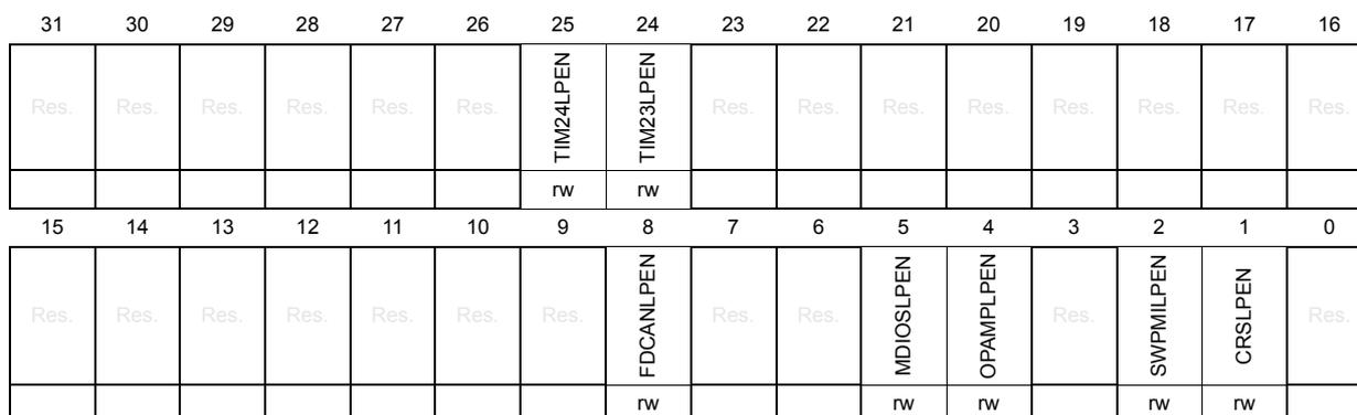
| 31 | 30 | 29 | 28 | 27 | 26 | 25 | 24 | 23 | 22 | 21 | 20 | 19 | 18 | 17 | 16 |
| Res. | Res. | Res. | Res. | Res. | Res. | TIM24LPEN | TIM23LPEN | Res. | Res. | Res. | Res. | Res. | Res. | Res. | Res. |
| rw | rw | ||||||||||||||
| 15 | 14 | 13 | 12 | 11 | 10 | 9 | 8 | 7 | 6 | 5 | 4 | 3 | 2 | 1 | 0 |
| Res. | Res. | Res. | Res. | Res. | Res. | Res. | FDCANLPEN | Res. | Res. | MDIOSLPEN | OPAMPLPEN | Res. | SWPMILPEN | CRSLPEN | Res. |
| rw | rw | rw | rw | rw |
Bits 31:26 Reserved, must be kept at reset value.
Bit 25 TIM24LPEN : TIM24 peripheral clocks enable during CSleep mode
Set and reset by software.
0: TIM24 peripheral clocks disabled during CSleep mode
1: TIM24 peripheral clocks enabled during CSleep mode (default after reset)
Bit 24 TIM23LPEN : TIM23 peripheral clocks enable during CSleep mode
Set and reset by software.
0: TIM23 peripheral clocks disabled during CSleep mode
1: TIM23 peripheral clocks enabled during CSleep mode (default after reset)
Bits 23:9 Reserved, must be kept at reset value.
Bit 8 FDCANLPEN : FDCAN Peripheral Clocks Enable During CSleep Mode
Set and reset by software.
0: FDCAN peripheral clocks disabled during CSleep mode
1: FDCAN peripheral clocks enabled during CSleep mode (default after reset)
The peripheral clocks of the FDCAN are: the kernel clock selected by FDCANSEL and provided to fdcan_ker_ck input, and the rcc_pclk1 bus interface clock.
Bits 7:6 Reserved, must be kept at reset value.
Bit 5 MDIOSLPEN : MDIOS peripheral clock enable during CSleep mode
Set and reset by software.
0: MDIOS peripheral clock disabled during CSleep mode
1: MDIOS peripheral clock enabled during CSleep mode (default after reset)
Bit 4 OPAMPLPEN : OPAMP peripheral clock enable during CSleep mode
Set and reset by software.
0: OPAMP peripheral clock disabled during CSleep mode
1: OPAMP peripheral clock enabled during CSleep mode (default after reset)
Bit 3 Reserved, must be kept at reset value.
Bit 2 SWPMILPEN : SWPMI Peripheral Clocks Enable During CSleep Mode
Set and reset by software.
0: SWPMI peripheral clocks disabled during CSleep mode
1: SWPMI peripheral clocks enabled during CSleep mode (default after reset)
The peripheral clocks of the SWPMI are: the kernel clock selected by SWPMISEL and provided to swpmi_ker_ck input, and the rcc_pclk1 bus interface clock.
Bit 1 CRSLPEN : Clock Recovery System peripheral clock enable during CSleep mode
Set and reset by software.
0: CRS peripheral clock disabled during CSleep mode
1: CRS peripheral clock enabled during CSleep mode (default after reset)
Bit 0 Reserved, must be kept at reset value.
8.7.55 RCC APB2 Sleep clock register (RCC_APB2LPENR)
This register can be accessed via two different offset address.
Table 78. RCC_APB2LPENR address offset and reset value
| Register Name | Address Offset | Reset Value |
|---|---|---|
| RCC_APB2LPENR | 0x118 | 0x4057 30F3 |
| RCC_C1_APB2LPENR | 0x178 |
| 31 | 30 | 29 | 28 | 27 | 26 | 25 | 24 | 23 | 22 | 21 | 20 | 19 | 18 | 17 | 16 |
| Res. | DFSDM1LPEN | Res. | Res. | Res. | Res. | Res. | Res. | Res. | SAI1LPEN | Res. | SPI5LPEN | Res. | TIM17LPEN | TIM16LPEN | TIM15LPEN |
| rw | rw | rw | rw | rw | rw | ||||||||||
| 15 | 14 | 13 | 12 | 11 | 10 | 9 | 8 | 7 | 6 | 5 | 4 | 3 | 2 | 1 | 0 |
| Res. | Res. | SPI4LPEN | SPI1LPEN | Res. | Res. | Res. | Res. | USART10LPEN | UART9LPEN | USART6LPEN | USART1LPEN | Res. | Res. | TIM8LPEN | TIM1LPEN |
| rw | rw | rw | rw | rw | rw | rw | rw |
Bit 31 Reserved, must be kept at reset value.
Bit 30 DFSDM1LPEN : DFSDM1 Peripheral Clocks Enable During CSleep Mode
Set and reset by software.
0: DFSDM1 peripheral clocks disabled during CSleep mode
1: DFSDM1 peripheral clocks enabled during CSleep mode (default after reset)
DFSDM1 peripheral clocks are: the kernel clocks selected by SAI1SEL and DFSDM1SEL and provided to Aclk and clk inputs respectively, and the rcc_pclk2 bus interface clock.
Bits 29:23 Reserved, must be kept at reset value.
Bit 22 SAI1LPEN : SAI1 Peripheral Clocks Enable During CSleep Mode
Set and reset by software.
0: SAI1 peripheral clocks disabled during CSleep mode
1: SAI1 peripheral clocks enabled during CSleep mode (default after reset)
The peripheral clocks of the SAI1 are: the kernel clock selected by SAI1SEL and provided to sai_a_ker_ck and sai_b_ker_ck inputs, and the rcc_pclk2 bus interface clock.
Bit 21 Reserved, must be kept at reset value.
Bit 20 SPI5LPEN : SPI5 Peripheral Clocks Enable During CSleep Mode
Set and reset by software.
0: SPI5 peripheral clocks disabled during CSleep mode
1: SPI5 peripheral clocks enabled during CSleep mode (default after reset)
The peripheral clocks of the SPI5 are: the kernel clock selected by SPI5SEL and provided to spi_ker_ck input, and the rcc_pclk2 bus interface clock.
Bit 19 Reserved, must be kept at reset value.
Bit 18 TIM17LPEN : TIM17 peripheral clock enable during CSleep mode
Set and reset by software.
0: TIM17 peripheral clock disabled during CSleep mode
1: TIM17 peripheral clock enabled during CSleep mode (default after reset)
Bit 17 TIM16LPEN : TIM16 peripheral clock enable during CSleep mode
Set and reset by software.
0: TIM16 peripheral clock disabled during CSleep mode
1: TIM16 peripheral clock enabled during CSleep mode (default after reset)
Bit 16 TIM15LPEN : TIM15 peripheral clock enable during CSleep mode
Set and reset by software.
0: TIM15 peripheral clock disabled during CSleep mode
1: TIM15 peripheral clock enabled during CSleep mode (default after reset)
Bits 15:14 Reserved, must be kept at reset value.
Bit 13 SPI4LPEN : SPI4 Peripheral Clocks Enable During CSleep Mode
Set and reset by software.
0: SPI4 peripheral clocks disabled during CSleep mode
1: SPI4 peripheral clocks enabled during CSleep mode (default after reset)
The peripheral clocks of the SPI4 are: the kernel clock selected by SPI45SEL and provided to spi_ker_ck input, and the rcc_pclk2 bus interface clock.
Bit 12 SPI1LPEN : SPI1 Peripheral Clocks Enable During CSleep Mode
Set and reset by software.
0: SPI1 peripheral clocks disabled during CSleep mode
1: SPI1 peripheral clocks enabled during CSleep mode (default after reset)
The peripheral clocks of the SPI1 are: the kernel clock selected by I2S123SRC and provided to spi_ker_ck input, and the rcc_pclk2 bus interface clock.
Bits 11:8 Reserved, must be kept at reset value.
Bit 7 USART10LPEN : USART10 peripheral clocks enable during CSleep mode
Set and reset by software.
0: USART10 peripheral clocks disabled during CSleep mode
1: USART10 peripheral clocks enabled during CSleep mode (default after reset)
The peripheral clocks of the USART10 are: the kernel clock selected by USART16910SEL and provided to usart_ker_ck input, and the rcc_pclk2 bus interface clock.
Bit 6 UART9LPEN : UART9 peripheral clocks enable during CSleep mode
Set and reset by software.
0: UART9 peripheral clocks disabled during CSleep mode
1: UART9 peripheral clocks enabled during CSleep mode (default after reset)
The peripheral clocks of the UART9 are: the kernel clock selected by USART16910SEL and provided to usart_ker_ck input, and the rcc_pclk2 bus interface clock.
Bit 5 USART6LPEN : USART6 Peripheral Clocks Enable During CSleep Mode
Set and reset by software.
0: USART6 peripheral clocks disabled during CSleep mode
1: USART6 peripheral clocks enabled during CSleep mode (default after reset)
The peripheral clocks of the USART6 are: the kernel clock selected by USART16910SEL and provided to usart_ker_ck input, and the rcc_pclk2 bus interface clock.
Bit 4 USART1LPEN : USART1 Peripheral Clocks Enable During CSleep Mode
Set and reset by software.
0: USART1 peripheral clocks disabled during CSleep mode
1: USART1 peripheral clocks enabled during CSleep mode (default after reset)
The peripheral clocks of the USART1 are: the kernel clock selected by USART16910SEL and provided to usart_ker_ck inputs, and the rcc_pclk2 bus interface clock.
Bits 3:2 Reserved, must be kept at reset value.
Bit 1 TIM8LPEN : TIM8 peripheral clock enable during CSleep mode
Set and reset by software.
0: TIM8 peripheral clock disabled during CSleep mode
1: TIM8 peripheral clock enabled during CSleep mode (default after reset)
Bit 0 TIM1LPEN : TIM1 peripheral clock enable during CSleep mode
Set and reset by software.
0: TIM1 peripheral clock disabled during CSleep mode
1: TIM1 peripheral clock enabled during CSleep mode (default after reset)
8.7.56 RCC APB4 Sleep clock register (RCC_APB4LPENR)
This register can be accessed via two different offset address.
Table 79. RCC_APB4LPENR address offset and reset value
| Register Name | Address Offset | Reset Value |
|---|---|---|
| RCC_APB4LPENR | 0x11C | 0x0421 DEAA |
| RCC_C1_APB4LPENR | 0x17C |
| 31 | 30 | 29 | 28 | 27 | 26 | 25 | 24 | 23 | 22 | 21 | 20 | 19 | 18 | 17 | 16 |
|---|---|---|---|---|---|---|---|---|---|---|---|---|---|---|---|
| Res. | Res. | Res. | Res. | Res. | DTSLPEN | Res. | Res. | Res. | Res. | SAI4LPEN | Res. | Res. | Res. | Res. | RTCAPBLPEN |
| rw | rw | rw | |||||||||||||
| 15 | 14 | 13 | 12 | 11 | 10 | 9 | 8 | 7 | 6 | 5 | 4 | 3 | 2 | 1 | 0 |
| VREFLPEN | COMP12LPEN | Res. | LPTIM5LPEN | LPTIM4LPEN | LPTIM3LPEN | LPTIM2LPEN | Res. | I2C4LPEN | Res. | SPI6LPEN | Res. | LPUART1LPEN | Res. | SYSCFGLPEN | Res. |
| rw | rw | rw | rw | rw | rw | rw | rw | rw | rw |
Bits 31:26 Reserved, must be kept at reset value.
Bit 26 DTSLPEN : Digital temperature sensor peripheral clock enable during CSleep mode
Set and reset by software.
0: Digital temperature sensor peripheral clock disabled during CSleep mode
1: Digital temperature sensor peripheral clock enabled during CSleep mode (default after reset)
Bits 25:22 Reserved, must be kept at reset value.
Bit 21 SAI4LPEN : SAI4 Peripheral Clocks Enable During CSleep Mode
Set and reset by software.
0: SAI4 peripheral clocks disabled during CSleep mode
1: SAI4 peripheral clocks enabled during CSleep mode (default after reset)
The peripheral clocks of the SAI4 are: the kernel clocks selected by SAI4ASEL and SAI4BSEL, and provided to sai_a_ker_ck and sai_b_ker_ck inputs respectively, and the rcc_pclk4 bus interface clock.
Bits 20:17 Reserved, must be kept at reset value.
Bit 16 RTCAPBLPEN : RTC APB Clock Enable During CSleep Mode
Set and reset by software.
0: The register clock interface of the RTC (APB) is disabled during CSleep mode
1: The register clock interface of the RTC (APB) is enabled during CSleep mode (default after reset)
Bit 15 VREFLPEN : VREF peripheral clock enable during CSleep mode
Set and reset by software.
0: VREF peripheral clock disabled during CSleep mode
1: VREF peripheral clock enabled during CSleep mode (default after reset)
Bit 14 COMP12LPEN : COMP1/2 peripheral clock enable during CSleep mode
Set and reset by software.
0: COMP1/2 peripheral clock disabled during CSleep mode
1: COMP1/2 peripheral clock enabled during CSleep mode (default after reset)
Bit 13 Reserved, must be kept at reset value.
Bit 12 LPTIM5LPEN : LPTIM5 Peripheral Clocks Enable During CSleep Mode
Set and reset by software.
0: LPTIM5 peripheral clocks disabled during CSleep mode
1: LPTIM5 peripheral clocks enabled during CSleep mode (default after reset)
The peripheral clocks of the LPTIM5 are: the kernel clock selected by LPTIM345SEL and provided to lptim_ker_ck input, and the rcc_pclk4 bus interface clock.
Bit 11 LPTIM4LPEN : LPTIM4 Peripheral Clocks Enable During CSleep Mode
Set and reset by software.
0: LPTIM4 peripheral clocks disabled during CSleep mode
1: LPTIM4 peripheral clocks enabled during CSleep mode (default after reset)
The peripheral clocks of the LPTIM4 are: the kernel clock selected by LPTIM345SEL and provided to lptim_ker_ck input, and the rcc_pclk4 bus interface clock.
Bit 10 LPTIM3LPEN : LPTIM3 Peripheral Clocks Enable During CSleep Mode
Set and reset by software.
0: LPTIM3 peripheral clocks disabled during CSleep mode
1: LPTIM3 peripheral clocks enabled during CSleep mode (default after reset)
The peripheral clocks of the LPTIM3 are: the kernel clock selected by LPTIM345SEL and provided to lptim_ker_ck input, and the rcc_pclk4 bus interface clock.
Bit 9 LPTIM2LPEN : LPTIM2 Peripheral Clocks Enable During CSleep Mode
Set and reset by software.
0: LPTIM2 peripheral clocks disabled during CSleep mode
1: LPTIM2 peripheral clocks enabled during CSleep mode (default after reset)
The peripheral clocks of the LPTIM5 are: the kernel clock selected by LPTIM2SEL and provided to lptim_ker_ck input, and the rcc_pclk4 bus interface clock.
Bit 8 Reserved, must be kept at reset value.
Bit 7 I2C4LPEN : I2C4 Peripheral Clocks Enable During CSleep Mode
Set and reset by software.
0: I2C4 peripheral clocks disabled during CSleep mode
1: I2C4 peripheral clocks enabled during CSleep mode (default after reset)
The peripheral clocks of the I2C4 are: the kernel clock selected by I2C4SEL and provided to i2c_ker_ck input, and the rcc_pclk4 bus interface clock.
Bit 6 Reserved, must be kept at reset value.
Bit 5 SPI6LPEN : SPI6 Peripheral Clocks Enable During CSleep Mode
Set and reset by software.
0: SPI6 peripheral clocks disabled during CSleep mode
1: SPI6 peripheral clocks enabled during CSleep mode (default after reset)
The peripheral clocks of the SPI6 are: the kernel clock selected by SPI6SEL and provided to spi_ker_ck input, and the rcc_pclk4 bus interface clock.
Bit 4 Reserved, must be kept at reset value.
Bit 3
LPUART1LPEN
: LPUART1 Peripheral Clocks Enable During CSleep Mode
Set and reset by software.
0: LPUART1 peripheral clocks disabled during CSleep mode
1: LPUART1 peripheral clocks enabled during CSleep mode (default after reset)
The peripheral clocks of the LPUART1 are: the kernel clock selected by LPUART1SEL and provided to
lpuart_ker_ck
input, and the
rcc_pclk4
bus interface clock.
Bit 2 Reserved, must be kept at reset value.
Bit 1
SYSCFGLPEN
: SYSCFG peripheral clock enable during CSleep mode
Set and reset by software.
0: SYSCFG peripheral clock disabled during CSleep mode
1: SYSCFG peripheral clock enabled during CSleep mode (default after reset)
Bit 0 Reserved, must be kept at reset value.
8.7.57 RCC register map
Table 80. RCC register map and reset values
| Offset | Register name | 31 | 30 | 29 | 28 | 27 | 26 | 25 | 24 | 23 | 22 | 21 | 20 | 19 | 18 | 17 | 16 | 15 | 14 | 13 | 12 | 11 | 10 | 9 | 8 | 7 | 6 | 5 | 4 | 3 | 2 | 1 | 0 | ||
|---|---|---|---|---|---|---|---|---|---|---|---|---|---|---|---|---|---|---|---|---|---|---|---|---|---|---|---|---|---|---|---|---|---|---|---|
| 0x000 | RCC_CR | Res. | Res. | PLL3RDY | PLL3ON | PLL2RDY | PLL2ON | PLL1RDY | PLL1ON | Res. | Res. | Res. | Res. | HSECSSON | HSEBYP | HSERDY | HSEON | D2CKRDY | D1CKRDY | HSI48RDY | HSI48ON | Res. | Res. | CSIKERON | CSIRDY | CSION | Res. | HSIDIVF | HSIDIV[1:0] | HSIRDY | HSIKERON | HSION | |||
| Reset value | 0 | 0 | 0 | 0 | 0 | 0 | 0 | 0 | 0 | 0 | 0 | 0 | 0 | 0 | 0 | 0 | 0 | 0 | 0 | 0 | 0 | 0 | 1 | ||||||||||||
| 0x004 | RCC_HSICFGR | Res. | HSITRIM[6:0] | Res. | Res. | Res. | Res. | Res. | Res. | Res. | Res. | Res. | Res. | Res. | Res. | HSICAL[11:0] | |||||||||||||||||||
| Reset value | 1 | 0 | 0 | 0 | 0 | 0 | 0 | X | X | X | X | X | X | X | X | X | X | X | X | ||||||||||||||||
| 0x008 | RCC_CRRCR | Res. | Res. | Res. | Res. | Res. | Res. | Res. | Res. | Res. | Res. | Res. | Res. | Res. | Res. | Res. | Res. | Res. | Res. | Res. | Res. | Res. | Res. | HSI48CAL[9:0] | |||||||||||
| Reset value | - | - | - | - | - | - | - | - | - | - | |||||||||||||||||||||||||
| 0x00C | reserved | Reserved | |||||||||||||||||||||||||||||||||
| 0x00C | RCC_CSICFGR | Res. | Res. | CSITRIM[5:0] | Res. | Res. | Res. | Res. | Res. | Res. | Res. | Res. | Res. | Res. | Res. | Res. | Res. | Res. | CSICAL[9:0] | ||||||||||||||||
| Reset value | 1 | 0 | 0 | 0 | 0 | 0 | X | X | X | X | X | X | X | X | X | X | |||||||||||||||||||
| 0x010 | RCC_CFGR | MCO2[2:0] | MCO2PRE[3:0] | MCO1[2:0] | MCO1PRE[3:0] | Res. | Res. | TIMPRE | Res. | Res. | Res. | RTCPRE[5:0] | STOPKERWUCK | STOPWUCK | SWS[2:0] | SW[2:0] | |||||||||||||||||||
| Reset value | 0 | 0 | 0 | 0 | 0 | 0 | 0 | 0 | 0 | 0 | 0 | 0 | 0 | 0 | 0 | 0 | 0 | 0 | 0 | 0 | 0 | 0 | 0 | 0 | 0 | 0 | 0 | 0 | |||||||
| 0x014 | reserved | Reserved | |||||||||||||||||||||||||||||||||
| 0x018 | RCC_D1CFGR | Res. | Res. | Res. | Res. | Res. | Res. | Res. | Res. | Res. | Res. | Res. | Res. | Res. | Res. | Res. | Res. | Res. | Res. | D1CPRE[3:0] | Res. | D1PPRE[2:0] | HPRE[3:0] | ||||||||||||
| Reset value | 0 | 0 | 0 | 0 | 0 | 0 | 0 | 0 | 0 | 0 | 0 | ||||||||||||||||||||||||
Table 80. RCC register map and reset values (continued)
| Offset | Register name | 31 | 30 | 29 | 28 | 27 | 26 | 25 | 24 | 23 | 22 | 21 | 20 | 19 | 18 | 17 | 16 | 15 | 14 | 13 | 12 | 11 | 10 | 9 | 8 | 7 | 6 | 5 | 4 | 3 | 2 | 1 | 0 |
|---|---|---|---|---|---|---|---|---|---|---|---|---|---|---|---|---|---|---|---|---|---|---|---|---|---|---|---|---|---|---|---|---|---|
| 0x01C | RCC_D2CFGR | Res. | Res. | Res. | Res. | Res. | Res. | Res. | Res. | Res. | Res. | Res. | Res. | Res. | Res. | Res. | Res. | Res. | Res. | Res. | Res. | Res. | D2PPRE2[2:0] | Res. | D2PPRE1[2:0] | Res. | Res. | Res. | Res. | Res. | |||
| Reset value | 0 | 0 | 0 | 0 | 0 | 0 | |||||||||||||||||||||||||||
| 0x020 | RCC_D3CFGR | Res. | Res. | Res. | Res. | Res. | Res. | Res. | Res. | Res. | Res. | Res. | Res. | Res. | Res. | Res. | Res. | Res. | Res. | Res. | Res. | Res. | D3PPRE2[2:0] | Res. | D3PPRE1[2:0] | Res. | Res. | Res. | Res. | Res. | |||
| Reset value | 0 | 0 | 0 | 0 | 0 | 0 | |||||||||||||||||||||||||||
| 0x024 | reserved | Reserved | |||||||||||||||||||||||||||||||
| 0x028 | RCC_PLLCKSEL | Res. | Res. | Res. | Res. | Res. | Res. | DIVM3[5:0] | Res. | Res. | DIVM2[5:0] | Res. | Res. | DIVM1[5:0] | Res. | Res. | PLL_SRC[1:0] | ||||||||||||||||
| Reset value | 1 | 0 | 0 | 0 | 0 | 0 | 1 | 0 | 0 | 0 | 0 | 0 | 1 | 0 | 0 | 0 | 0 | 0 | 0 | 0 | |||||||||||||
| 0x02C | RCC_PLLCFGR | Res. | Res. | Res. | Res. | Res. | Res. | Res. | Res. | Res. | Res. | Res. | Res. | Res. | Res. | Res. | Res. | Res. | Res. | Res. | Res. | Res. | Res. | PLL3RGE[1:0] | PLL3VCOSEL | PLL3FRACEN | PLL2RGE[1:0] | PLL2VCOSEL | PLL2FRACEN | PLL1RGE[1:0] | PLL1VCOSEL | PLL1FRACEN | |
| Reset value | 0 | 0 | 0 | 0 | 0 | 0 | 0 | 0 | 0 | 0 | |||||||||||||||||||||||
| 0x030 | RCC_PLL1DIVR | Res. | DIVR1[6:0] | Res. | DIVQ1[6:0] | DIVP1[6:0] | DIVN1[8:0] | ||||||||||||||||||||||||||
| Reset value | 0 | 0 | 0 | 0 | 0 | 0 | 1 | 0 | 0 | 0 | 0 | 0 | 0 | 1 | 0 | 0 | 0 | 0 | 0 | 0 | 0 | 1 | 0 | 1 | 0 | 0 | 0 | 0 | 0 | 0 | 0 | ||
| 0x034 | RCC_PLL1FRACR | Res. | Res. | Res. | Res. | Res. | Res. | Res. | Res. | Res. | Res. | Res. | Res. | Res. | Res. | Res. | Res. | FRACN1[12:0] | Res. | Res. | Res. | Res. | |||||||||||
| Reset value | 0 | 0 | 0 | 0 | 0 | 0 | 0 | 0 | 0 | 0 | 0 | 0 | 0 | 0 | 0 | ||||||||||||||||||
| 0x038 | RCC_PLL2DIVR | Res. | DIVR2[6:0] | Res. | DIVQ2[6:0] | DIVP2[6:0] | DIVN2[8:0] | ||||||||||||||||||||||||||
| Reset value | 0 | 0 | 0 | 0 | 0 | 0 | 1 | 0 | 0 | 0 | 0 | 0 | 0 | 1 | 0 | 0 | 0 | 0 | 0 | 0 | 0 | 1 | 0 | 1 | 0 | 0 | 0 | 0 | 0 | 0 | 0 | ||
| 0x03C | RCC_PLL2FRACR | Res. | Res. | Res. | Res. | Res. | Res. | Res. | Res. | Res. | Res. | Res. | Res. | Res. | Res. | Res. | Res. | FRACN2[12:0] | Res. | Res. | Res. | Res. | |||||||||||
| Reset value | 0 | 0 | 0 | 0 | 0 | 0 | 0 | 0 | 0 | 0 | 0 | 0 | 0 | 0 | 0 | ||||||||||||||||||
| 0x040 | RCC_PLL3DIVR | Res. | DIVR3[6:0] | Res. | DIVQ3[6:0] | DIVP3[6:0] | DIVN3[8:0] | ||||||||||||||||||||||||||
| Reset value | 0 | 0 | 0 | 0 | 0 | 0 | 1 | 0 | 0 | 0 | 0 | 0 | 0 | 1 | 0 | 0 | 0 | 0 | 0 | 0 | 0 | 1 | 0 | 1 | 0 | 0 | 0 | 0 | 0 | 0 | 0 | ||
| 0x044 | RCC_PLL3FRACR | Res. | Res. | Res. | Res. | Res. | Res. | Res. | Res. | Res. | Res. | Res. | Res. | Res. | Res. | Res. | Res. | FRACN3[12:0] | Res. | Res. | Res. | Res. | |||||||||||
| Reset value | 0 | 0 | 0 | 0 | 0 | 0 | 0 | 0 | 0 | 0 | 0 | 0 | 0 | 0 | 0 | ||||||||||||||||||
| 0x048 | reserved | Reserved | |||||||||||||||||||||||||||||||
| 0x04C | RCC_D1CCIPR | Res. | Res. | CKPERSEL[1:0] | Res. | Res. | Res. | Res. | Res. | Res. | Res. | Res. | Res. | Res. | SDMMCSEL | Res. | Res. | Res. | Res. | Res. | Res. | Res. | Res. | Res. | Res. | Res. | OCTOSPISSEL[1:0] | Res. | Res. | FMCSEL[1:0] | |||
| Reset value | 0 | 0 | 0 | 0 | 0 | 0 | 0 | ||||||||||||||||||||||||||
Table 80. RCC register map and reset values (continued)
| Offset | Register name | 31 | 30 | 29 | 28 | 27 | 26 | 25 | 24 | 23 | 22 | 21 | 20 | 19 | 18 | 17 | 16 | 15 | 14 | 13 | 12 | 11 | 10 | 9 | 8 | 7 | 6 | 5 | 4 | 3 | 2 | 1 | 0 | |
|---|---|---|---|---|---|---|---|---|---|---|---|---|---|---|---|---|---|---|---|---|---|---|---|---|---|---|---|---|---|---|---|---|---|---|
| 0x050 | RCC_D2CCIP1R | SWPMISEL | Res. | FDCANSEL[1:0] | Res. | Res. | Res. | DFSDM1SEL | Res. | Res. | Res. | SPDIFRXSEL[1:0] | Res. | Res. | Res. | SP145SEL[2:0] | Res. | Res. | Res. | SP1123SEL[2:0] | Res. | Res. | Res. | Res. | Res. | Res. | Res. | Res. | Res. | Res. | Res. | Res. | SAI1SEL[2:0] | |
| Reset value | 0 | 0 0 | 0 | 0 0 | 0 0 0 | 0 0 0 | 0 0 0 | |||||||||||||||||||||||||||
| 0x054 | RCC_D2CCIP2R | Res. | LPTIM1SEL[2:0] | Res. | Res. | Res. | Res. | Res. | CECSEL[1:0] | USBSEL[1:0] | Res. | Res. | Res. | Res. | Res. | Res. | Res. | I2C123SEL[1:0] | Res. | Res. | Res. | USART16910SEL[2:0] | USART234578SEL[2:0] | |||||||||||
| Reset value | 0 0 0 | 0 0 | 0 0 | 0 0 | 0 0 0 | 0 0 0 | ||||||||||||||||||||||||||||
| 0x058 | RCC_D3CCIPR | Res. | SP6SEL[2:0] | Res. | Res. | Res. | SAI4BSEL[2:0] | Res. | Res. | Res. | SAI4ASEL[2:0] | Res. | Res. | Res. | ADCSEL[1:0] | Res. | Res. | Res. | LPTIM345SEL[2:0] | Res. | Res. | Res. | LPJUART1SEL[2:0] | |||||||||||
| Reset value | 0 0 0 | 0 0 0 | 0 0 0 | 0 0 0 | 0 0 0 | 0 0 0 | ||||||||||||||||||||||||||||
| 0x05C | reserved | Reserved | ||||||||||||||||||||||||||||||||
| 0x060 | RCC_CIER | Res. | Res. | Res. | Res. | Res. | Res. | Res. | Res. | Res. | Res. | Res. | Res. | Res. | Res. | Res. | Res. | Res. | Res. | Res. | Res. | Res. | Res. | LSECCSSIE | PLL3RDYIE | PLL2RDYIE | PLL1RDYIE | HSI48RDYIE | CSIRDYIE | HSERDYIE | HSIRDYIE | LSERDYIE | LSIRDYIE | |
| Reset value | 0 | 0 | 0 | 0 | 0 | 0 | 0 | 0 | 0 | 0 | ||||||||||||||||||||||||
| 0x064 | RCC_CIFR | Res. | Res. | Res. | Res. | Res. | Res. | Res. | Res. | Res. | Res. | Res. | Res. | Res. | Res. | Res. | Res. | Res. | Res. | Res. | Res. | Res. | Res. | HSECCSSF | LSECCSSF | PLL3RDYF | PLL2RDYF | PLL1RDYF | HSI48RDYF | CSIRDYF | HSERDYF | HSIRDYF | LSERDYF | LSIRDYF |
| Reset value | 0 | 0 | 0 | 0 | 0 | 0 | 0 | 0 | 0 | 0 | ||||||||||||||||||||||||
| 0x068 | RCC_CICR | Res. | Res. | Res. | Res. | Res. | Res. | Res. | Res. | Res. | Res. | Res. | Res. | Res. | Res. | Res. | Res. | Res. | Res. | Res. | Res. | Res. | Res. | HSECCSSC | LSECCSSC | PLL3RDYC | PLL2RDYC | PLL1RDYC | HSI48RDYC | CSIRDYC | HSERDYC | HSIRDYC | LSERDYC | LSIRDYC |
| Reset value | 0 | 0 | 0 | 0 | 0 | 0 | 0 | 0 | 0 | 0 | ||||||||||||||||||||||||
| 0x06C | reserved | Reserved | ||||||||||||||||||||||||||||||||
| 0x070 | RCC_BDCR | Res. | Res. | Res. | Res. | Res. | Res. | Res. | Res. | Res. | Res. | Res. | Res. | Res. | Res. | Res. | BDRST | RTCEN | Res. | Res. | Res. | Res. | Res. | Res. | Res. | RTCOSEL[1:0] | Res. | LSECCSSD | LSECCSSON | LSEDRV[1:0] | LSEBYP | LSERDY | LSEON | |
| Reset value | 0 | 0 | 0 0 | 0 | 0 | 0 0 | 0 | 0 | 0 | |||||||||||||||||||||||||
Table 80. RCC register map and reset values (continued)
| Offset | Register name | 31 | 30 | 29 | 28 | 27 | 26 | 25 | 24 | 23 | 22 | 21 | 20 | 19 | 18 | 17 | 16 | 15 | 14 | 13 | 12 | 11 | 10 | 9 | 8 | 7 | 6 | 5 | 4 | 3 | 2 | 1 | 0 |
|---|---|---|---|---|---|---|---|---|---|---|---|---|---|---|---|---|---|---|---|---|---|---|---|---|---|---|---|---|---|---|---|---|---|
| 0x074 | RCC_CSR | Res. | Res. | Res. | Res. | Res. | Res. | Res. | Res. | Res. | Res. | Res. | Res. | Res. | Res. | Res. | Res. | Res. | Res. | Res. | Res. | Res. | Res. | Res. | Res. | Res. | Res. | Res. | Res. | Res. | Res. | LSIRDY | LSION |
| Reset value | 0 | 0 | |||||||||||||||||||||||||||||||
| 0x078 | reserved | Reserved | |||||||||||||||||||||||||||||||
| 0x07C | RCC_AHB3RSTR | CPURST | Res. | Res. | Res. | Res. | Res. | Res. | Res. | OTFD2RST | OTFD1RST | OMNGRST | Res. | OCTOSPI2RST | Res. | Res. | SDMMC1RST | Res. | Res. | Res. | FMCRST | Res. | Res. | Res. | Res. | Res. | Res. | Res. | DMA2DRST | Res. | Res. | Res. | MDMARST |
| Reset value | 0 | 0 | 0 | 0 | 0 | 0 | 0 | 0 | 0 | ||||||||||||||||||||||||
| 0x080 | RCC_AHB1RSTR | Res. | Res. | Res. | Res. | Res. | Res. | USB1OTGRST | Res. | Res. | Res. | Res. | Res. | Res. | Res. | Res. | ETH1MACRST | Res. | Res. | Res. | Res. | Res. | Res. | Res. | Res. | Res. | Res. | ADC12RST | Res. | Res. | Res. | DMA2RST | DMA1RST |
| Reset value | 0 | 0 | 0 | 0 | 0 | ||||||||||||||||||||||||||||
| 0x084 | RCC_AHB2RSTR | Res. | Res. | Res. | Res. | Res. | Res. | Res. | Res. | Res. | Res. | Res. | Res. | CORDICRST | FMACRST | Res. | Res. | Res. | Res. | Res. | Res. | Res. | Res. | SDMMC2RST | Res. | Res. | RNGRST | HASHRST | CRYPTRST | Res. | Res. | Res. | DCM_PSSIRS |
| Reset value | 0 | 0 | 0 | 0 | 0 | 0 | 0 | ||||||||||||||||||||||||||
| 0x088 | RCC_AHB4RSTR | Res. | Res. | Res. | Res. | Res. | Res. | HSEMRST | ADC3RST | Res. | Res. | Res. | Res. | Res. | Res. | Res. | Res. | Res. | Res. | Res. | Res. | Res. | GPIOKRST | GPIOJRST | Res. | GPIOHRST | GPIOGRST | GPIOFRST | GPIOERST | GPIODRST | GPIOCRST | GPIOBRST | GPIOARST |
| Reset value | 0 | 0 | 0 | 0 | 0 | 0 | 0 | 0 | 0 | 0 | 0 | 0 | |||||||||||||||||||||
| 0x08C | RCC_APB3RSTR | Res. | Res. | Res. | Res. | Res. | Res. | Res. | Res. | Res. | Res. | Res. | Res. | Res. | Res. | Res. | Res. | Res. | Res. | Res. | Res. | Res. | Res. | Res. | Res. | Res. | Res. | Res. | LTDRCRST | Res. | Res. | Res. | Res. |
| Reset value | 0 | ||||||||||||||||||||||||||||||||
| 0x090 | RCC_APB1LSTR | UART8RST | UART7RST | DAC12RST | Res. | CECRST | Res. | I2C5RST | Res. | I2C3RST | I2C2RST | I2C1RST | UART5RST | UART4RST | USART3RST | USART2RST | SPDIFRXRST | SPI3RST | SPI2RST | Res. | Res. | Res. | Res. | LPTIM1RST | TIM14RST | TIM13RST | TIM12RST | TIM7RST | TIM6RST | TIM5RST | TIM4RST | TIM3RST | TIM2RST |
| Reset value | 0 | 0 | 0 | 0 | 0 | 0 | 0 | 0 | 0 | 0 | 0 | 0 | 0 | 0 | 0 | 0 | 0 | 0 | 0 | 0 | 0 | 0 | 0 | 0 | 0 | ||||||||
| 0x094 | RCC_APB1HRSTR | Res. | Res. | Res. | Res. | Res. | Res. | TIM24RST | TIM23RST | Res. | Res. | Res. | Res. | Res. | Res. | Res. | Res. | Res. | Res. | Res. | Res. | Res. | Res. | Res. | FDCANRST | Res. | Res. | MDIOSRST | OPAMPFRST | Res. | SWMPPIRST | CRSRST | Res. |
| Reset value | 0 | 0 | 0 | 0 | 0 | 0 | 0 | ||||||||||||||||||||||||||
Table 80. RCC register map and reset values (continued)
| Offset | Register name | 31 | 30 | 29 | 28 | 27 | 26 | 25 | 24 | 23 | 22 | 21 | 20 | 19 | 18 | 17 | 16 | 15 | 14 | 13 | 12 | 11 | 10 | 9 | 8 | 7 | 6 | 5 | 4 | 3 | 2 | 1 | 0 | |
|---|---|---|---|---|---|---|---|---|---|---|---|---|---|---|---|---|---|---|---|---|---|---|---|---|---|---|---|---|---|---|---|---|---|---|
| 0x098 | RCC_APB2RSTR | Res. | DFSDM1RST | Res. | Res. | Res. | Res. | Res. | Res. | Res. | SAI1RST | Res. | SPI5RST | Res. | TIM17RST | TIM16RST | TIM15RST | Res. | Res. | SP4RST | SP1RST | Res. | Res. | Res. | Res. | Res. | UART10RST | UART9RST | USART6RST | USART1RST | Res. | Res. | TIM8RST | TIM1RST |
| Reset value | 0 | 0 | 0 | 0 | 0 | 0 | 0 | 0 | 0 | 0 | 0 | 0 | 0 | 0 | ||||||||||||||||||||
| 0x09C | RCC_APB4RSTR | Res. | Res. | Res. | Res. | Res. | DTISRST | Res. | Res. | Res. | Res. | SAI4RST | Res. | Res. | Res. | Res. | Res. | VREFRST | COMP12RST | Res. | LPTIM5RST | LPTIM4RST | LPTIM3RST | LPTIM2RST | Res. | I2C4RST | Res. | SP16RST | Res. | LPUART1RST | Res. | Res. | SYSCFGGRST | Res. |
| Reset value | 0 | 0 | 0 | 0 | 0 | 0 | 0 | 0 | 0 | 0 | 0 | 0 | ||||||||||||||||||||||
| 0x0A0 | RCC_GCR | Res. | Res. | Res. | Res. | Res. | Res. | Res. | Res. | Res. | Res. | Res. | Res. | Res. | Res. | Res. | Res. | Res. | Res. | Res. | Res. | Res. | Res. | Res. | Res. | Res. | Res. | Res. | Res. | Res. | Res. | Res. | WW1RSC | |
| Reset value | 0 | |||||||||||||||||||||||||||||||||
| 0x0A4 | reserved | Reserved | ||||||||||||||||||||||||||||||||
| 0x0A8 | RCC_D3AMR | Res. | Res. | SRAM4AMEN | BKPRAMAMEN | Res. | DTSAMEN | Res. | ADC3AMEN | Res. | Res. | SAI4AMEN | Res. | CRCAMEN | Res. | Res. | RTCAMEN | VREFAMEN | COMP12AMEN | Res. | LPTIM5AMEN | LPTIM4AMEN | LPTIM3AMEN | LPTIM2AMEN | Res. | I2C4AMEN | Res. | Res. | SP16AMEN | Res. | LPUART1AMEN | Res. | Res. | BDMAAMEN |
| Reset value | 0 | 0 | 0 | 0 | 0 | 0 | 0 | 0 | 0 | 0 | 0 | 0 | 0 | 0 | 0 | 0 | 0 | |||||||||||||||||
| 0x0AC to 0x0CC | reserved | Reserved | ||||||||||||||||||||||||||||||||
| 0x0D0 | RCC_RSR | Res. | LPWRRSTF | Res. | WWDG1RSTF | Res. | TWDG1RSTF | Res. | SFTRSTF | PORRSTF | PINRSTF | BORRSTF | D2RSTF | D1RSTF | Res. | CPURSTF | RMVF | Res. | Res. | Res. | Res. | Res. | Res. | Res. | Res. | Res. | Res. | Res. | Res. | Res. | Res. | Res. | Res. | |
| Reset value | 0 | 0 | 0 | 0 | 1 | 1 | 1 | 1 | 1 | 1 | 0 | |||||||||||||||||||||||
| 0x0D4 | RCC_AHB3ENR | Res. | Res. | Res. | Res. | Res. | Res. | Res. | Res. | OTFD2EN | OTFD1EN | IOMNGREN | Res. | OCTO2EN | Res. | Res. | SDMMC1EN | Res. | OCTO1EN | Res. | FMCEN | Res. | Res. | Res. | Res. | Res. | Res. | Res. | DMA2DEN | Res. | Res. | Res. | MDMAEN | |
| Reset value | 0 | 0 | 0 | 0 | 0 | 0 | 0 | 0 | 0 | |||||||||||||||||||||||||
| 0x0D8 | RCC_AHB1ENR | Res. | Res. | Res. | Res. | Res. | USB1OTGHSEN | USB1OTGHSEN | Res. | Res. | Res. | Res. | Res. | Res. | Res. | ETH1RXEN | ETH1TXEN | ETH1MACEN | Res. | Res. | Res. | Res. | Res. | Res. | Res. | Res. | Res. | ADC12EN | Res. | Res. | Res. | DMA2EN | DMA1EN | |
| Reset value | 0 | 0 | 0 | 0 | 0 | 0 | 0 | 0 | ||||||||||||||||||||||||||
Table 80. RCC register map and reset values (continued)
| Offset | Register name | 31 | 30 | 29 | 28 | 27 | 26 | 25 | 24 | 23 | 22 | 21 | 20 | 19 | 18 | 17 | 16 | 15 | 14 | 13 | 12 | 11 | 10 | 9 | 8 | 7 | 6 | 5 | 4 | 3 | 2 | 1 | 0 |
|---|---|---|---|---|---|---|---|---|---|---|---|---|---|---|---|---|---|---|---|---|---|---|---|---|---|---|---|---|---|---|---|---|---|
| 0x0DC | RCC_AHB2ENR | Res. | SRAM2EN | SRAM1EN | Res. | Res. | Res. | Res. | Res. | Res. | Res. | Res. | Res. | Res. | Res. | CORIDIEN | FMACEN | Res. | Res. | Res. | Res. | Res. | Res. | SDMMC2EN | Res. | Res. | RNGEN | HASHEN | CRYPTEN | Res. | Res. | Res. | DCMI_PSSIE |
| Reset value | 0 | 0 | 0 | 0 | 0 | 0 | 0 | 0 | 0 | ||||||||||||||||||||||||
| 0x0E0 | RCC_AHB4ENR | Res. | Res. | Res. | Res. | Res. | Res. | Res. | Res. | Res. | Res. | Res. | Res. | Res. | Res. | Res. | Res. | Res. | Res. | Res. | Res. | Res. | Res. | Res. | Res. | Res. | Res. | Res. | Res. | Res. | Res. | Res. | Res. |
| Reset value | |||||||||||||||||||||||||||||||||
| 0x0E4 | RCC_APB3ENR | Res. | Res. | Res. | Res. | Res. | Res. | Res. | Res. | Res. | Res. | Res. | Res. | Res. | Res. | Res. | Res. | Res. | Res. | Res. | Res. | Res. | Res. | Res. | Res. | Res. | Res. | Res. | Res. | Res. | Res. | Res. | Res. |
| Reset value | |||||||||||||||||||||||||||||||||
| 0x0E8 | RCC_APB1ENR | UART8EN | UART7EN | DAC12EN | Res. | CECEN | Res. | I2C5EN | Res. | I2C3EN | I2C2EN | I2C1EN | UART5EN | UART4EN | USART3EN | USART2EN | SPDIFRXEN | SP13EN | SP12EN | Res. | Res. | Res. | Res. | LPTIM1EN | TIM14EN | TIM13EN | TIM12EN | TIM7EN | TIM6EN | TIM5EN | TIM4EN | TIM3EN | TIM2EN |
| Reset value | 0 | 0 | 0 | 0 | 0 | 0 | 0 | 0 | 0 | 0 | 0 | 0 | 0 | 0 | 0 | 0 | 0 | 0 | 0 | 0 | 0 | 0 | 0 | 0 | 0 | ||||||||
| 0x0EC | RCC_APB1HENR | Res. | Res. | Res. | Res. | Res. | Res. | Res. | Res. | Res. | Res. | Res. | Res. | Res. | Res. | Res. | Res. | Res. | Res. | Res. | Res. | Res. | Res. | Res. | Res. | Res. | Res. | Res. | Res. | Res. | Res. | Res. | Res. |
| Reset value | |||||||||||||||||||||||||||||||||
| 0x0F0 | RCC_APB2ENR | Res. | Res. | Res. | Res. | Res. | Res. | Res. | Res. | Res. | Res. | Res. | Res. | Res. | Res. | Res. | Res. | Res. | Res. | Res. | Res. | Res. | Res. | Res. | Res. | Res. | Res. | Res. | Res. | Res. | Res. | Res. | Res. |
| Reset value | |||||||||||||||||||||||||||||||||
| 0x0F4 | RCC_APB4ENR | Res. | Res. | Res. | Res. | Res. | Res. | Res. | Res. | Res. | Res. | Res. | Res. | Res. | Res. | Res. | Res. | Res. | Res. | Res. | Res. | Res. | Res. | Res. | Res. | Res. | Res. | Res. | Res. | Res. | Res. | Res. | Res. |
| Reset value | |||||||||||||||||||||||||||||||||
| 0x0F8 | reserved | Reserved | |||||||||||||||||||||||||||||||
| 0x0FC | RCC_AHB3LPENR | AXISRAM1LPEN | ITCM1LPEN | DTCM2LPEN | DTCM1LPEN | Res. | Res. | Res. | Res. | OTFD2LPEN | OTFD1LPEN | IOMNGRLPEN | Res. | SDMMC1LPEN | Res. | SDMMC1LPEN | Res. | OCTO1LPEN | Res. | FMCLPEN | Res. | Res. | Res. | Res. | FLASHLPEN | Res. | Res. | Res. | Res. | DMA2DLPEN | Res. | Res. | MDMALPEN |
| Reset value | 1 | 1 | 1 | 1 | 1 | 1 | 1 | 1 | 1 | 1 | 1 | 1 | 1 | 1 | |||||||||||||||||||
Table 80. RCC register map and reset values (continued)
| Offset | Register name | 31 | 30 | 29 | 28 | 27 | 26 | 25 | 24 | 23 | 22 | 21 | 20 | 19 | 18 | 17 | 16 | 15 | 14 | 13 | 12 | 11 | 10 | 9 | 8 | 7 | 6 | 5 | 4 | 3 | 2 | 1 | 0 | |
|---|---|---|---|---|---|---|---|---|---|---|---|---|---|---|---|---|---|---|---|---|---|---|---|---|---|---|---|---|---|---|---|---|---|---|
| 0x100 | RCC_AHB1LPENR | Res. | Res. | Res. | Res. | Res. | USB1OTGHSULPILPEN | Res. | Res. | Res. | Res. | Res. | Res. | Res. | Res. | ETH1RXLPEN | ETH1TXLPEN | ETH1MACLPEN | Res. | Res. | Res. | Res. | Res. | Res. | Res. | Res. | Res. | Res. | ADC12LPEN | Res. | Res. | Res. | DMA2LPEN | |
| Reset value | 1 | 1 | 1 | 1 | 1 | 1 | ||||||||||||||||||||||||||||
| 0x104 | RCC_AHB2LPENR | Res. | SRAM2LPEN | SRAM1LPEN | Res. | Res. | Res. | Res. | Res. | Res. | Res. | Res. | Res. | Res. | Res. | CORCDLPEN | FMACLPEN | Res. | Res. | Res. | Res. | Res. | Res. | SDMMC2LPEN | Res. | Res. | RNGLPEN | HASHLPEN | CRYPTLPEN | Res. | Res. | Res. | DCMI_PSSILPEN | |
| Reset value | 1 | 1 | 1 | 1 | 1 | 1 | 1 | 1 | 1 | |||||||||||||||||||||||||
| 0x108 | RCC_AHB4LPENR | Res. | Res. | SRAM4LPEN | BKPRAMLPEN | Res. | Res. | ADC3LPEN | Res. | Res. | Res. | Res. | Res. | Res. | Res. | Res. | Res. | Res. | Res. | Res. | Res. | Res. | Res. | GPIO1LPEN | GPIO2LPEN | GPIO3LPEN | GPIO4LPEN | GPIO5LPEN | GPIO6LPEN | GPIO7LPEN | GPIO8LPEN | GPIO9LPEN | GPIO10LPEN | |
| Reset value | 1 | 1 | 1 | 1 | 1 | 1 | 1 | 1 | 1 | 1 | 1 | 1 | ||||||||||||||||||||||
| 0x10C | RCC_APB3LPENR | Res. | Res. | Res. | Res. | Res. | Res. | Res. | Res. | Res. | Res. | Res. | Res. | Res. | Res. | Res. | Res. | Res. | Res. | Res. | Res. | Res. | Res. | Res. | Res. | Res. | Res. | Res. | Res. | Res. | Res. | Res. | Res. | |
| Reset value | ||||||||||||||||||||||||||||||||||
| 0x110 | RCC_APB1LLPENR | UART8LPEN | UART7LPEN | DAC12LPEN | Res. | CECLPEN | Res. | I2C5LPEN | Res. | I2C3LPEN | I2C2LPEN | I2C1LPEN | UART5LPEN | UART4LPEN | USART3LPEN | USART2LPEN | SPDIFRXLPEN | SPI3LPEN | SPI2LPEN | Res. | Res. | Res. | Res. | LPTIM1LPEN | TIM14LPEN | TIM13LPEN | TIM12LPEN | TIM7LPEN | TIM6LPEN | TIM5LPEN | TIM4LPEN | TIM3LPEN | TIM2LPEN | |
| Reset value | 1 | 1 | 1 | 1 | 1 | 1 | 1 | 1 | 1 | 1 | 1 | 1 | 1 | 1 | 1 | 1 | 1 | 1 | 1 | 1 | 1 | 1 | 1 | 1 | 1 | |||||||||
| 0x114 | RCC_APB1HLPENR | Res. | Res. | Res. | Res. | Res. | TIM24LPEN | TIM23LPEN | Res. | Res. | Res. | Res. | Res. | Res. | Res. | Res. | Res. | Res. | Res. | Res. | Res. | Res. | Res. | Res. | Res. | Res. | Res. | Res. | Res. | Res. | Res. | Res. | Res. | Res. |
| Reset value | 1 | 1 | ||||||||||||||||||||||||||||||||
| 0x118 | RCC_APB2LPENR | Res. | DFSDM1LPEN | Res. | Res. | Res. | Res. | Res. | Res. | Res. | SAHLPEN | Res. | SPI5LPEN | Res. | TIM17LPEN | TIM16LPEN | TIM15LPEN | Res. | Res. | SPI4LPEN | SPI1LPEN | Res. | Res. | Res. | Res. | Res. | Res. | USART10LPEN | USART9LPEN | USART6LPEN | USART1LPEN | Res. | Res. | |
| Reset value | 1 | 1 | 1 | 1 | 1 | 1 | 1 | 1 | 1 | 1 | 1 | 1 | 1 |
Table 80. RCC register map and reset values (continued)
| Offset | Register name | 31 | 30 | 29 | 28 | 27 | 26 | 25 | 24 | 23 | 22 | 21 | 20 | 19 | 18 | 17 | 16 | 15 | 14 | 13 | 12 | 11 | 10 | 9 | 8 | 7 | 6 | 5 | 4 | 3 | 2 | 1 | 0 |
|---|---|---|---|---|---|---|---|---|---|---|---|---|---|---|---|---|---|---|---|---|---|---|---|---|---|---|---|---|---|---|---|---|---|
| 0x11C | RCC_ APB4LPENR | Res. | Res. | Res. | Res. | Res. | DTSLPEN | Res. | Res. | Res. | Res. | SA4LPEN | Res. | Res. | Res. | Res. | RTCAPBLPEN | VREFLPEN | COMP12LPEN | Res. | LPTIM5LPEN | LPTIM4LPEN | LPTIM3LPEN | LPTIM2LPEN | Res. | I2C4LPEN | Res. | SPI6LPEN | Res. | LPUART1LPEN | Res. | SYSCFGLPEN | Res. |
| Reset value | 1 | 1 | 1 | 1 | 1 | 1 | 1 | 1 | 1 | 1 | 1 | 1 | 1 | ||||||||||||||||||||
| 0x120 to 0x12C | reserved | Reserved | |||||||||||||||||||||||||||||||
| 0x130 | RCC_C1_RSR | Res. | LPWRRSTF | Res. | WWDG1RSTF | Res. | IWDG1RSTF | Res. | SFTRSTF | PORRSTF | PINRSTF | BORRSTF | D2RSTF | D1RSTF | Res. | CPURSTF | RMVF | Res. | Res. | Res. | Res. | Res. | Res. | Res. | Res. | Res. | Res. | Res. | Res. | Res. | Res. | Res. | Res. |
| Reset value | 0 | 0 | 0 | 0 | 1 | 1 | 1 | 1 | 1 | 1 | 0 | ||||||||||||||||||||||
| 0x134 | RCC_C1_ AHB3ENR | Res. | Res. | Res. | Res. | Res. | Res. | Res. | Res. | OTFD2EN | OTFD1EN | IOMNGREN | Res. | OCTO2EN | Res. | Res. | SDMMC1EN | Res. | OCTO1EN | Res. | FMCPEN | Res. | Res. | Res. | Res. | Res. | Res. | Res. | DMA2DEN | Res. | Res. | Res. | MDMAEN |
| Reset value | 0 | 0 | 0 | 0 | 0 | 0 | 0 | 0 | 0 | ||||||||||||||||||||||||
| 0x138 | RCC_C1_ AHB1ENR | Res. | Res. | Res. | Res. | Res. | USB1OTGHSULPEN | USB1OTGHSEN | Res. | Res. | Res. | Res. | Res. | Res. | Res. | ETH1RXEN | ETH1TXEN | ETH1MACEN | Res. | Res. | Res. | Res. | Res. | Res. | Res. | Res. | Res. | ADC12EN | Res. | Res. | Res. | DMA2EN | DMA1EN |
| Reset value | 0 | 0 | 0 | 0 | 0 | 0 | 0 | 0 | |||||||||||||||||||||||||
| 0x13C | RCC_C1_ AHB2ENR | Res. | SRAM2EN | SRAM1EN | Res. | Res. | Res. | Res. | Res. | Res. | Res. | Res. | Res. | Res. | Res. | CORDICEN | FMACEN | Res. | Res. | Res. | Res. | Res. | SDMMC2EN | Res. | Res. | Res. | RNGEN | HASHEN | CRYPTEN | Res. | Res. | DCMI_PSS1EN | |
| Reset value | 0 | 0 | 0 | 0 | 0 | 0 | 0 | 0 | 0 | ||||||||||||||||||||||||
| 0x140 | RCC_C1_ AHB4ENR | Res. | Res. | Res. | BKPRAMEN | Res. | Res. | HSEMEN | ADC3EN | Res. | Res. | BDMAEN | Res. | CRCEN | Res. | Res. | Res. | Res. | Res. | Res. | Res. | GPIOEN | GPIOJEN | Res. | Res. | GPIOHEN | GPIOGEN | GPIOFEN | GPIOEEN | GIOPDEN | GIOPCEN | GIOPBEN | GIOPAEN |
| Reset value | 0 | 0 | 0 | 0 | 0 | 0 | 0 | 0 | 0 | 0 | 0 | 0 | 0 | 0 | 0 | ||||||||||||||||||
| 0x144 | RCC_C1_ APB3ENR | Res. | Res. | Res. | Res. | Res. | Res. | Res. | Res. | Res. | Res. | Res. | Res. | Res. | Res. | Res. | Res. | Res. | Res. | Res. | Res. | Res. | Res. | Res. | Res. | WWDG1EN | Res. | Res. | Res. | LTDCCEN | Res. | Res. | Res. |
| Reset value | 0 | 0 | |||||||||||||||||||||||||||||||
Table 80. RCC register map and reset values (continued)
| Offset | Register name | 31 | 30 | 29 | 28 | 27 | 26 | 25 | 24 | 23 | 22 | 21 | 20 | 19 | 18 | 17 | 16 | 15 | 14 | 13 | 12 | 11 | 10 | 9 | 8 | 7 | 6 | 5 | 4 | 3 | 2 | 1 | 0 |
|---|---|---|---|---|---|---|---|---|---|---|---|---|---|---|---|---|---|---|---|---|---|---|---|---|---|---|---|---|---|---|---|---|---|
| 0x148 | RCC_C1_APB1LENR | UART8EN | UART7EN | DAC12EN | Res. | CECEN | Res. | I2C5EN | Res. | I2C3EN | I2C2EN | I2C1EN | UART5EN | UART4EN | USART3EN | USART2EN | SPDIFRXEN | SPI3EN | SPI2EN | Res. | Res. | Res. | Res. | LPTIM1EN | TIM14EN | TIM13EN | TIM12EN | TIM7EN | TIM6EN | TIM5EN | TIM4EN | TIM3EN | TIM2EN |
| Reset value | 0 | 0 | 0 | 0 | 0 | 0 | 0 | 0 | 0 | 0 | 0 | 0 | 0 | 0 | 0 | 0 | 0 | 0 | 0 | 0 | 0 | 0 | 0 | 0 | 0 | ||||||||
| 0x14C | RCC_C1_APB1HENR | Res. | Res. | Res. | Res. | Res. | Res. | TIM24EN | TIM23EN | Res. | Res. | Res. | Res. | Res. | Res. | Res. | Res. | Res. | Res. | Res. | Res. | Res. | Res. | Res. | FDCANEN | Res. | Res. | MDIOSEN | OPAMPEN | Res. | SWPMIEN | CRSEN | Res. |
| Reset value | 0 | 0 | 0 | 0 | 0 | 0 | 0 | ||||||||||||||||||||||||||
| 0x150 | RCC_C1_APB2ENR | Res. | DFSDM1EN | Res. | Res. | Res. | Res. | Res. | Res. | SA1EN | Res. | Res. | SP5EN | Res. | TIM17EN | TIM16EN | TIM15EN | Res. | Res. | SP4EN | SP1EN | Res. | Res. | Res. | Res. | USART10EN | USART9EN | USART6EN | USART1EN | Res. | Res. | TIM8EN | TIM1EN |
| Reset value | 0 | 0 | 0 | 0 | 0 | 0 | 0 | 0 | 0 | 0 | 0 | 0 | 0 | 0 | |||||||||||||||||||
| 0x154 | RCC_C1_APB4ENR | Res. | Res. | Res. | Res. | Res. | DTSEN | Res. | Res. | Res. | Res. | SA4EN | Res. | Res. | Res. | Res. | RTCAPBEN | VREFEN | COMP12EN | Res. | LPTIM5EN | LPTIM4EN | LPTIM3EN | LPTIM2EN | Res. | I2C4EN | Reserved | SPI6EN | Res. | LPUART1EN | Res. | SYSCFGEN | Res. |
| Reset value | 0 | 0 | 1 | 0 | 0 | 0 | 0 | 0 | 0 | 0 | 0 | 0 | 0 | 0 | 0 | 0 | 0 | ||||||||||||||||
| 0x158 | reserved | Reserved | |||||||||||||||||||||||||||||||
| 0x15C | RCC_C1_AHB3LPENR | AXISRAM1LPEN | ITCMLPEN | DTCM2LPEN | DTCM1LPEN | Res. | Res. | Res. | Res. | OTFD2LPEN | OTFD1LPEN | IOMNGRLPEN | Res. | SDMMC1LPEN | Res. | Res. | SDMMC1LPEN | Res. | OCTOT1LPEN | Res. | FMCLPEN | Res. | Res. | Res. | FLASHLPEN | Res. | Res. | Res. | DMA2LPEN | Res. | Res. | Res. | MDMALPEN |
| Reset value | 1 | 1 | 1 | 1 | 1 | 1 | 1 | 1 | 1 | 1 | 1 | 1 | 1 | 1 | |||||||||||||||||||
| 0x160 | RCC_C1_AHB1LPENR | Res. | Res. | Res. | Res. | Res. | USB1OTGHSULPILPEN | USB1OTGHSILPEN | Res. | Res. | Res. | Res. | Res. | Res. | ETH1RXLPEN | ETH1TXLPEN | ETH1MACLPEN | Res. | Res. | Res. | Res. | Res. | Res. | Res. | Res. | Res. | Res. | ADC12LPEN | Res. | Res. | Res. | DMA2LPEN | DMA1LPEN |
| Reset value | 1 | 1 | 1 | 1 | 1 | 1 | 1 | 1 | |||||||||||||||||||||||||
| 0x164 | RCC_C1_AHB2LPENR | Res. | SRAM2LPEN | SRAM1LPEN | Res. | Res. | Res. | Res. | Res. | Res. | Res. | Res. | Res. | Res. | CORDICLPEN | FMACLPEN | Res. | Res. | Res. | Res. | Res. | Res. | Res. | SDMMC2LPEN | Res. | Res. | RNGLPEN | HASHPEN | CRYPTLPEN | Res. | Res. | Res. | DCMI_PSSILPEN |
| Reset value | 1 | 1 | 1 | 1 | 1 | 1 | 1 | 1 | 1 | ||||||||||||||||||||||||
Table 80. RCC register map and reset values (continued)
| Offset | Register name | 31 | 30 | 29 | 28 | 27 | 26 | 25 | 24 | 23 | 22 | 21 | 20 | 19 | 18 | 17 | 16 | 15 | 14 | 13 | 12 | 11 | 10 | 9 | 8 | 7 | 6 | 5 | 4 | 3 | 2 | 1 | 0 | |
|---|---|---|---|---|---|---|---|---|---|---|---|---|---|---|---|---|---|---|---|---|---|---|---|---|---|---|---|---|---|---|---|---|---|---|
| 0x168 | RCC_C1_AHB4LPENR | Res. | Res. | SRAM4LPEN | BKPRAMLPEN | Res. | Res. | Res. | ADC3LPEN | Res. | Res. | BDMALPEN | Res. | CRCLPEN | Res. | Res. | Res. | Res. | Res. | Res. | Res. | Res. | GPIO1LPEN | GPIOJLPEN | Res. | GPIOHLPEN | GPIOGLPEN | GPIOFLPEN | GPIOELPEN | GPIODLPEN | GPIOCLPEN | GPIOBLPEN | GPIOALPEN | |
| Reset value | 1 | 1 | 1 | 1 | 1 | 1 | 1 | 1 | 1 | 1 | 1 | 1 | 1 | 1 | 1 | |||||||||||||||||||
| 0x16C | RCC_C1_APB3LPENR | Res. | Res. | Res. | Res. | Res. | Res. | Res. | Res. | Res. | Res. | Res. | Res. | Res. | Res. | Res. | Res. | Res. | Res. | Res. | Res. | Res. | Res. | Res. | Res. | Res. | WWDG1LPEN | Res. | Res. | Res. | LTDCLPEN | Res. | Res. | Res. |
| Reset value | 1 | 1 | ||||||||||||||||||||||||||||||||
| 0x170 | RCC_C1_APB1LLPENR | UART8LPEN | UART7LPEN | DAC12LPEN | Res. | CECLPEN | Res. | I2C5LPEN | Res. | I2C3LPEN | I2C2LPEN | I2C1LPEN | UART5LPEN | UART4LPEN | USART3LPEN | USART2LPEN | SPDIFRXLPEN | SPI3LPEN | SPI2LPEN | Res. | Res. | Res. | Res. | LPTIM1LPEN | TIM14LPEN | TIM13LPEN | TIM12LPEN | TIM7LPEN | TIM6LPEN | TIM5LPEN | TIM4LPEN | TIM3LPEN | TIM2LPEN | |
| Reset value | 1 | 1 | 1 | 1 | 1 | 1 | 1 | 1 | 1 | 1 | 1 | 1 | 1 | 1 | 1 | 1 | 1 | 1 | 1 | 1 | 1 | 1 | 1 | 1 | 1 | |||||||||
| 0x174 | RCC_C1_APB1HLPENR | Res. | Res. | Res. | Res. | Res. | Res. | TIM24LPEN | TIM23LPEN | Res. | Res. | Res. | Res. | Res. | Res. | Res. | Res. | Res. | Res. | Res. | Res. | Res. | Res. | Res. | FDCANLPEN | Res. | Res. | MDIOSLPEN | OPAMP1LPEN | Res. | SWPMILPEN | CRSLPEN | Res. | Res. |
| Reset value | 1 | 1 | 1 | 1 | 1 | 1 | 1 | |||||||||||||||||||||||||||
| 0x178 | RCC_C1_APB2LPENR | Res. | DFSDM1LPEN | Res. | Res. | Res. | Res. | Res. | Res. | Res. | SA1LPEN | Res. | SPI5LPEN | Res. | TIM17LPEN | TIM16LPEN | TIM15LPEN | Res. | Res. | SPI4LPEN | SPI1LPEN | Res. | Res. | Res. | Res. | USART10LPEN | USART9LPEN | USART8LPEN | USART1LPEN | Res. | Res. | TIM8LPEN | TIM1LPEN | |
| Reset value | 1 | 1 | 1 | 1 | 1 | 1 | 1 | 1 | 1 | 1 | 1 | 1 | 1 | 1 | ||||||||||||||||||||
| 0x17C | RCC_C1_APB4LPENR | Res. | Res. | Res. | Res. | Res. | Res. | DTSLPEN | Res. | Res. | Res. | SA4LPEN | Res. | Res. | Res. | Res. | Res. | Res. | Res. | Res. | Res. | Res. | Res. | Res. | Res. | Res. | Res. | Res. | Res. | Res. | Res. | Res. | Res. | Res. |
| Reset value | 1 | 1 | ||||||||||||||||||||||||||||||||
| 0x180 to 0x1FC | reserved | Reserved | ||||||||||||||||||||||||||||||||
Refer to Section 2.3 on page 131 for the register boundary addresses.