6. Reset and clock control (RCC)
6.1 Reset
There are three types of reset, defined as system reset, power reset and backup domain reset.
6.1.1 Power reset
A power reset is generated when one of the following events occurs:
- • a Brownout reset (BOR)
- • when exiting from Standby mode
- • when exiting from Shutdown mode
A Brownout reset, including power-on or power-down reset (POR/PDR), sets all registers to their reset values except the backup domain.
When exiting Standby mode, all registers in the \( V_{CORE} \) domain are set to their reset value. Registers outside the \( V_{CORE} \) domain (RTC, WKUP, IWDG and Standby/Shutdown modes control) are not impacted.
When exiting Shutdown mode, a Brownout reset is generated, resetting all registers except those in the backup domain.
6.1.2 System reset
A system reset sets all registers to their reset values unless otherwise specified in the register description.
A system reset is generated when one of the following events occurs:
- • a low level on the NRST pin (external reset)
- • window watchdog event (WWDG reset)
- • independent watchdog event (IWDG reset)
- • a software reset (SW reset) (see Software reset )
- • low-power mode security reset (see Low-power mode security reset )
- • option byte loader reset (see Option byte loader reset )
- • a Brownout reset
- • an illegal sub-GHz radio access (sub-GHz radio protocol error reset) (only valid for non LoRa devices, STM32WLE4xx)
The reset source can be identified by checking the reset flags in the control/status register,
RCC_CSR
(see
Section 6.4.31: RCC control/status register (RCC_CSR)
).
These sources act on the NRST pin, that is always kept low during the delay phase. The CPU RESET service routine vector is selected via the BOOT0 and BOOT1.
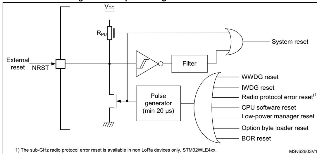
The system reset signal provided to the device is output on the NRST pin. The pulse generator guarantees a minimum reset pulse duration of 20 µs for each internal reset source. In case of an external reset, the reset pulse is generated while the NRST pin is asserted low.
In case of an internal reset, the internal pull-up \( R_{PU} \) is deactivated in order to save the power consumption through the pull-up resistor.
Figure 20. Simplified diagram of the reset circuit
Software reset
The SYSRESETREQ bit in CPU application interrupt and reset control register may be set to force a software reset on the device (refer to the programming manual STM32 Cortex®-M4 MCUs and MPUs (PM0214)).
Low-power mode security reset
To prevent that critical applications mistakenly enter a low-power mode, two low-power mode security resets are available.
If enabled in option bytes, the resets are generated in the following conditions:
- • Entering Standby mode: this type of reset is enabled by resetting nRST_STDBY bit in user option bytes. In this case, whenever a Standby mode entry sequence is successfully executed, the device is reset instead of entering Standby mode.
- • Entering Stop mode: this type of reset is enabled by resetting nRST_STOP bit in user option bytes. In this case, whenever a Stop mode entry sequence is successfully executed, the device is reset instead of entering Stop mode.
- • Entering Shutdown mode: this type of reset is enabled by resetting nRST_SHDW bit in user option bytes. In this case, whenever a Shutdown mode entry sequence is successfully executed, the device is reset instead of entering Shutdown mode.
For further information on the user option bytes, refer to Section 3.4.1: Option bytes description .
Option byte loader reset
The option byte loader reset is generated when the OBL_LAUNCH bit is set in the FLASH_CR register. This bit is used to launch the option byte loading by software.
6.1.3 Backup domain reset
The backup domain has two specific resets.
A backup domain reset is generated when one of the following events occurs:
- • a software reset, triggered by setting the BDRST bit in the RCC backup domain control register (RCC_BDCR)
- • \( V_{DD} \) or \( V_{BAT} \) power on, if both supplies have previously been powered off
A backup domain reset only affects the LSE oscillator, the RTC, the backup registers and the RCC backup domain control register.
6.1.4 Sub-GHz radio reset
The sub-GHz radio can be reset by the RFRST register bit. A sub-GHz radio reset status flag is provided in the RFRSTF register bit. The sub-GHz radio must not be accessed as long as the reset status flag RFRSTF indicates sub-GHz radio in reset.
The sub-GHz radio is also reset when entering Shutdown mode.
6.1.5 PKA SRAM reset
The PKA SRAM is erased by hardware on any power reset and system reset. The status of the PKA SRAM erase operation can be monitored in SYSCFG_SCSR.PKASRAMBSY flag register bit.
6.2 Clocks
The following different clock sources can be used to drive the system clock (SYSCLK):
- • HSI16 (high-speed internal) 16 MHz RC oscillator clock
- • MSI (multi-speed internal) RC oscillator clock from 100 kHz to 48 MHz
- • HSE32 (high-speed external) 32 MHz oscillator clock, with trimming capacitors.
- • PLL clock
The MSI is used as system clock source after startup from reset, configured at 4 MHz.
The devices have the following additional clock sources:
- • LSI: 32 kHz low-speed internal RC that may drive the independent watchdog and optionally the RTC used for auto-wake-up from Stop and Standby modes.
- • LSE: 32.768 kHz low-speed external crystal that optionally drives the RTC used for auto-wake-up from Stop, Standby and Shutdown modes, or the real-time clock (RTCCLK).
Each clock source can be switched on or off independently when it is not used, to optimize power consumption.
Several prescalers can be used to configure the AHB frequencies (HCLK3/PCLK3, HCLK1), the high-speed APB2 (PCLK2) and the low-speed APB1 (PCLK1) domains. The maximum frequency of the AHB (HCLK3, HCLK1), the PCLK1 and the PCLK2 domains is 48 MHz.
Most peripheral clocks are derived from their bus clock (HCLK, PCLK) except the following:
- • The clock used for true RNG, is derived (selected by software) from one of the following sources:
- – PLL VCO (PLLQCLK) (only available in Run mode)
- – MSI (only available in Run mode)
- – LSI clock
- – LSE clock
- • The ADC clock is derived (selected by software) from one of the following sources:
- – system clock (SYSCLK) (only available in Run mode)
- – HSI16 clock (only available in Run mode)
- – PLL VCO (PLLPCLK) (only available in Run mode)
- • The DAC uses the LSI clock in sample and hold mode
- • The (LP)U(S)ARTs clocks are derived (selected by software) from one of the following sources:
- – system clock (SYSCLK) (only available in Run mode)
- – HSI16 clock (available in Run and Stop modes)
- – LSE clock (available in Run and Stop modes)
- – APB clock (PCLK depending on which APB the U(S)ART is mapped) (available in CRun and CSleep when also enabled in (LP)U(S)ARTxSMEN.)
The wake-up from Stop mode is supported only when the clock is HSI16 or LSE.
- • The I2Cs clocks are derived (selected by software) from one of the following sources:
- – system clock (SYSCLK) (only available in Run mode)
- – HSI16 clock (available in Run and Stop modes)
- – APB clock (PCLK depending on which APB the I2C is mapped) (available in CRun and CSleep when also enabled in I2CxSMEN.)
The wake-up from Stop mode is supported only when the clock is HSI16.
- • The SPI2S2 I2S clock is derived (selected by software) from one of the following sources:
- – HSI16 clock (only available in Run mode)
- – PLL VCO (PLLQCLK) (only available in Run mode)
- – external input I2S_CK (available in Run and Stop modes)
- – The SPI2S2 clock in SPI mode is provided by PCLK1 clock.
- – I2S mode is selected through register SPIx_I2SCFGR I2SMOD field
- • The low-power timers (LPTIMx) clock is derived (selected by software) from one of the following sources:
- – LSI clock (available in Run and Stop modes)
- – LSE clock (available in Run and Stop modes)
- – HSI16 clock (only available in Run mode)
- – APB clock (PCLK depending on which APB the LPTIMx is mapped) (available in Run and CStop when enabled in LPTIMxSMEN.)
- – external clock mapped on LPTIMx_IN1 (available in Run and Stop modes)
The functionality in Stop mode (including wake-up) is supported only when the clock is LSI or LSE, or in external clock mode.
- • The RTC clock is derived (selected by software) from one of the following sources:
- – LSE clock
- – LSI clock
- – HSE32 clock divided by 32
The functionality in Stop mode (including wake-up) is supported only when the clock is LSI or LSE.
- • The IWDG clock is always the LSI clock.
The RCC feeds the CPU system timer (SysTick) external clock with the AHB clock (HCLK1) divided by eight. The SysTick can work either with this clock or directly with the CPU clock (HCLK1), configurable in the SysTick control and status register.
FCLK1 acts as CPU free-running clock. For more details, refer to the programming manual STM32 Cortex®-M4 MCUs and MPUs programming manual (PM0214) .
Figure 21. Clock tree
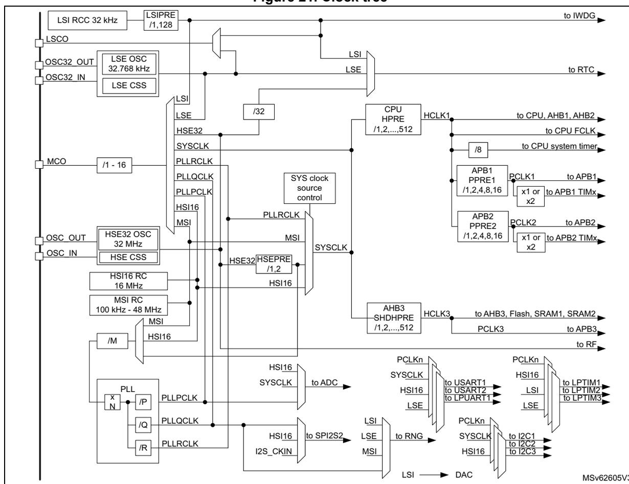
The diagram illustrates the clock tree architecture. On the left, external and internal clock sources are shown:
- External sources: LSCO (connected to LSI), OSC32_OUT/OSC32_IN (connected to LSE OSC 32.768 kHz and LSE CSS), OSC_OUT/OSC_IN (connected to HSE32 OSC 32 MHz and HSE CSS), HSI16 RC 16 MHz, and MSI RC 100 kHz - 48 MHz.
- Internal sources: LSI RCC 32 kHz (divided by LSIPRE /1,128 for IWDG), HSE32 (divided by /32 for SYSCLK), and PLL (with X/N, /P, /Q, /R dividers).
- HCLK1: Derived from SYSCLK via CPU HPRE (/1,2,...,512). It feeds the CPU, AHB1, AHB2, and is divided by /8 for the CPU system timer.
- HCLK3: Derived from SYSCLK via AHB3 SHDHPRE (/1,2,...,512). It feeds AHB3, Flash, SRAM1, SRAM2, and is divided into PCLK3 for APB3 and RF.
- PCLK1 and PCLK2: Derived from HCLK1 via APB1 PPRE1 and APB2 PPRE2 (/1,2,4,8,16). They feed APB1, APB2, and their respective timers (TIMx), with options for x1 or x2 multiplication.
- Other peripherals:
- ADC: Fed by SYSCLK or HSI16.
- SPI2/SPI3: Fed by HSI16 or I2S_CKIN.
- RNG: Fed by LSI, LSE, or MSI.
- USART1/2 and LPUART1: Fed by PCLK1, HSI16, LSI, or LSE.
- LPTIM1/2/3: Fed by PCLK1, HSI16, LSI, or LSE.
- I2C1/2/3: Fed by PCLK1, SYSCLK, or HSI16.
- DAC: Fed by LSI.
- 1. For full details about the internal and external clock source characteristics, refer to the electrical characteristics section in the device datasheet.
- 2. The ADC clock can additionally be derived from the AHB clock of the ADC bus interface, divided by a programmable factor (1, 2 or 4). When the programmable factor is 1, the AHB prescaler must be equal to 1.
6.2.1 HSE32 clock with trimming
The HSE32 32 MHz external oscillator has the advantage of producing a very accurate rate on the main clock. The HSE32 furthermore provides on-chip trimming capability.
The high-speed external clock signal (HSE32) can be generated from the following clock sources:
- • HSE32 external crystal
- • HSE32 external clock
- – external clock source
- – external TCXO
The clock source must be placed as close as possible to the oscillator pins in order to minimize output distortion and startup stabilization time.
HSE32 is controlled from the CPU and from the sub-GHz radio (see Section 4: Sub-GHz radio (SUBGHZ) ).
HSE32 can be switched on and off using the HSEON bit in the RCC clock control register (RCC_CR) . The HSE32 clock sources can be either an external crystal (XTAL) or an external source including a temperature compensated crystal oscillator (TCXO). HSE32 must be enabled with the HSEON bit when used for the CPU.
The stability of the XTAL HSE32 clock may be impacted by the sub-GHz radio, depending on the transmit output power (max +22 dBm), heating up the device. Heating depends on the used transmit output power and the device package. Careful PCB design using thermal heat dissipation techniques must be applied to avoid heat transfer to the HSE32 reference clock source. For the HSE32 frequency drift requirements related to the sub-GHz radio, see Section 4.5.1: LoRa modem .
The HSERDY flag in the RCC clock control register (RCC_CR) indicates if the HSE32 oscillator is stable or not. At startup, the clock is not released until this bit is set by hardware. An interrupt can be generated if enabled in the RCC clock interrupt enable register (RCC_CIER) .
The sub-GHz radio enables HSE32 autonomously for its own purpose, independently of the HSEON bit.
Warning: The HSE32 cannot be used in LPRun mode.
Figure 22. HSE32 clock sources
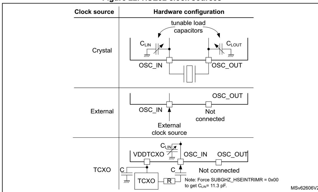
| Clock source | Hardware configuration |
|---|---|
| Crystal | |
| External | |
| TCXO |
External crystal (HSE32 crystal)
The associated hardware configuration is shown in Figure 22 . Refer to the electrical characteristics section of the datasheet for more details.
Frequency trimming
When using HSE32 with external crystal, the load capacitors are provided by the integrated capacitor banks, that can be trimmed. The HSE32 load capacitor trimming allows a compensation of device manufacturing process variations, used crystal and PCB design. The HSE32 frequency can be tuned in the application via the sub-GHz radio registers SUBGHZ_HSEINTRIMR and SUBGHZ_HSEOUTRIMR. For more information see Section 4.4: Sub-GHz radio clocks .
The HSE32 frequency can be measured by outputting the HSE32 clock on the MCO when in Run mode.
External source (HSE32 TXCO)
In this mode, an external TXCO clock source must be provided. This external source frequency must be 32 MHz. This mode is selected by setting the HSEBYP_PWR and HSEON bits in the RCC clock control register (RCC_CR) . The external clock signal (refer to the datasheet) must drive the following pins (see Figure 22: HSE32 clock sources ):
- • OSC_IN and OSC_OUT pins: OSC_IN pin must be driven, while the OSC_OUT pin must be left not connected.
The TCXO supply can be provided by the device on PB0/VDDTCXO. The V DDTCXO supply is also enabled with the HSEBYP_PWR bit in RCC clock control register (RCC_CR) before enabling the HSE32 oscillator. V DDTCXO supply level and TCXO clock startup timeout can be configured through the sub-GHz radio Set_TcxoMode() command (see Section 4: Sub-GHz radio (SUBGHZ) for more details).
Figure 23. HSE32 TCXO control
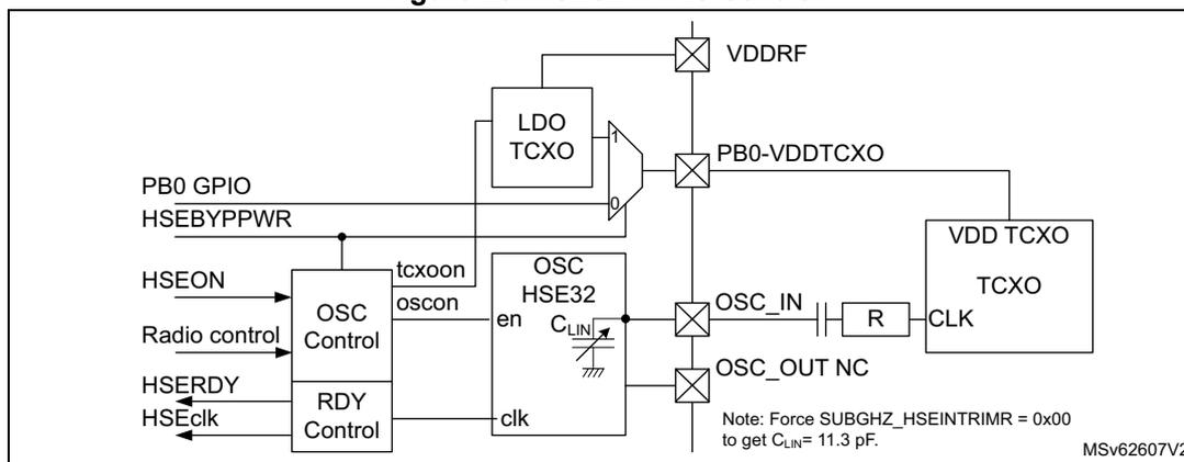
The control of the HSE32 external TCXO can be done in the following ways:
- • powered by
\(
V_{DDTCXO}
\)
:
- – Set the voltage level inside the sub-GHz radio by using the
Set_TcxoMode()command, before enabling the \( V_{DDTCXO} \) regulator. - – Set the HSEBYP PWR bit to 1 to use the \( V_{DDTCXO} \) regulator.
- – Enable the HSE32 use with external TCXO in Run mode for the CPU with the HSEON bit. The availability of the clock can be checked with the HSERDY bit.
- – Enable the HSE32 use with TXC XO for the sub-GHz radio with the sub-GHz radio
Set_TcxoMode()command when in sub-GHz radio Standby mode. It is recommended to issue a sub-GHz radio calibration command once the HSE32 clock is available.
- – Set the voltage level inside the sub-GHz radio by using the
When the CPU is in one of the low-power modes (Stop, Standby, or Shutdown) and the sub-GHz radio is in Sleep, the HSE32 clock including the TCXO is disabled.
6.2.2 HSI16 clock
The HSI16 clock signal is generated from an internal 16 MHz Oscillator.
The HSI16 oscillator has the advantage of providing a clock source at low cost. It also has a faster startup time than the HSE32 crystal oscillator however, even with calibration the frequency is less accurate than an external crystal oscillator or ceramic resonator.
The HSI16 clock can be selected as system clock after wake-up from Stop modes (Stop 0, Stop 1 or Stop 2). Refer to Section 6.3 . It can also be used as a backup clock source (auxiliary clock) if the HSE32 crystal oscillator fails. Refer to Section 6.2.10 .
Calibration
The RC oscillator frequencies can vary from one chip to another due to manufacturing process variations. This is why each device is factory calibrated by ST for 1 % accuracy at \( T_A = 25^\circ C \) .
After a reset, the factory calibration value is loaded in the HSICAL[7:0] bits in the RCC internal clock sources calibration register (RCC_ICSCR) .
If the application is subject to voltage or temperature variations, this may affect the RC oscillator speed. The HSI16 frequency can be trimmed in the application using the HSITRIM[6:0] bits in the RCC internal clock sources calibration register (RCC_ICSCR) .
For more details on how to measure the HSI16 frequency variation, refer to Section 6.2.20 .
The HSIRDY flag in the RCC clock control register (RCC_CR) indicates if the HSI16 RC is stable or not. At startup, the HSI16 RC output clock is not released until this bit is set by hardware.
The HSI16 RC can be switched on and off using the HSION bit in the RCC clock control register (RCC_CR) .
The HSI16 signal can also be used as a backup source (Auxiliary clock) if the HSE32 crystal oscillator fails. Refer to Section 6.2.10 .
6.2.3 MSI clock
The MSI clock signal is generated from an internal RC oscillator. Its frequency range can be adjusted by software using the MSIRANGE[3:0] bits in the RCC clock control register (RCC_CR) . The following frequency ranges are available: 100 kHz, 200 kHz, 400 kHz, 800 kHz, 1 MHz, 2 MHz, 4 MHz (default value), 8 MHz, 16 MHz, 24 MHz, 32 MHz and 48 MHz. To use the MSI range, it must be selected by MSIRGSEL.
The MSI clock is used as system clock after restart from reset, wake-up from Standby and Shutdown low-power modes. After restart from Reset and Shutdown, the MSI frequency is set to its default value 4 MHz (see Section 6.3 ). When wake-up from Standby, MSI can be adjusted by software using the MSISRANGE[3:0] bits in the RCC control/status register (RCC_CSR) . The following frequency ranges are available: 1MHz, 2 MHz, 4 MHz (default value) and 8 MHz.
The MSI clock can be selected as system clock after a wake-up from Stop mode (Stop 0, Stop 1, or Stop 2, see Section 6.3 ). It can also be used as a backup clock source (auxiliary clock for the CPU) if the HSE32 crystal oscillator fails (see Section 6.2.10 ).
The MSI RC oscillator provides a low-power clock source. In addition, when used in PLL-mode with the LSE, it also provides a very accurate clock source that can be used to feed the PLL to run the system at the maximum speed 48 MHz.
The MSIRDY flag in the RCC clock control register (RCC_CR) indicates whether the MSI RC is stable or not. At startup, the MSI RC output clock is not released until this bit is set by hardware. The MSI RC can be switched on and off by using the MSION bit in the RCC clock control register (RCC_CR) .
Hardware auto calibration with LSE (PLL-mode)
When a 32.768 kHz external oscillator is present in the application, it is possible to configure the MSI in a PLL-mode by setting the MSIPLLEN bit in the RCC clock control register (RCC_CR) . When configured in PLL-mode, MSI automatically calibrates itself thanks to the LSE. This mode is available for all MSI frequency ranges.
Software calibration
The MSI RC oscillator frequency can vary from one chip to another due to manufacturing process variations. This is why each device is factory calibrated by ST for 1 % accuracy at an ambient temperature \( T_A = 25\text{ }^\circ\text{C} \) . After reset, the factory calibration value is loaded in the MSICAL[7:0] bits in the RCC internal clock sources calibration register (RCC_ICSCR) . If the application is subject to voltage or temperature variations, this may affect the RC oscillator speed. The MSI frequency can be trimmed in the application using the MSITRIM[7:0] bits in the RCC internal clock sources calibration register (RCC_ICSCR) . For more details on how to measure the MSI frequency variation, refer to Section 6.2.20 .
6.2.4 PLL
The device embeds one PLL. The PLL provides up to three independent outputs. The internal PLL can be used to multiply the HSI16, HSE32 or MSI output clock frequency. The PLL input frequency must be between 2.66 and 16 MHz. The selected clock source is divided by a programmable factor PLLM from 1 to 8 to provide a clock frequency in the requested input range. Refer to Figure 21 and RCC PLL configuration register (RCC_PLLCFGR) .
The PLL configuration (selection of the input clock and multiplication factor) must be done before enabling the PLL. Once the PLL is enabled, these parameters cannot be changed.
To modify the PLL configuration, proceed as follows:
- 1. Disable the PLL by setting PLLON to 0 in the RCC clock control register (RCC_CR) .
- 2. Wait until PLLRDY is cleared. The PLL is now fully stopped.
- 3. Change the desired parameter.
- 4. Enable the PLL again by setting PLLON to 1.
- 5. Enable the desired PLL outputs by configuring PLLPEN, PLLQEN, PLLREN in the RCC PLL configuration register (RCC_PLLCFGR) .
An interrupt can be generated when the PLL is ready, if enabled in the RCC clock interrupt enable register (RCC_CIER) .
The PLLQCLK and PLLRCLK output frequency must not exceed 48 MHz. The PLLPCLK output frequency must not exceed 62 MHz.
The enable bits of the PLL output clock (PLLPEN, PLLQEN, PLLREN) can be modified at any time without stopping the PLL. PLLREN cannot be cleared if PLLRCLK is used as system clock.
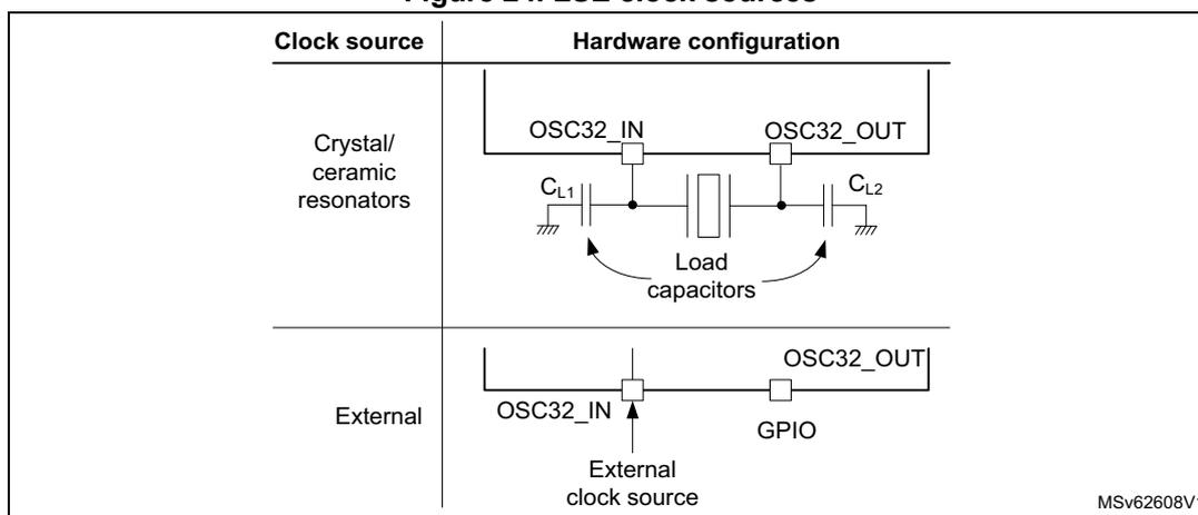
6.2.5 LSE clock
The LSE crystal is a 32.768 kHz low-speed external crystal or ceramic resonator. It provides a low-power but highly accurate clock source to the real-time clock peripheral (RTC) for clock/calendar or other timing functions.
The resonator and the load capacitors must be placed as close as possible to the oscillator pins in order to minimize output distortion and startup stabilization time. The loading capacitance values must be adjusted according to the selected oscillator.
Figure 24. LSE clock sources
| Clock source | Hardware configuration |
|---|---|
| Crystal/ ceramic resonators | |
| External |
MSV62608V1
The LSE crystal is switched on and off using the LSEON bit in the RCC backup domain control register (RCC_BDCR) . The crystal oscillator driving strength can be changed at runtime using the LSEDRV[1:0] bits in the RCC backup domain control register (RCC_BDCR) to obtain the best compromise between robustness and short start-up time on one side and low-power-consumption on the other side. The LSE drive can be decreased to the lower drive capability (LSEDRV = 0) when the LSE is on. However, once LSEDRV is selected, the drive capability can not be increased if LSEON = 1.
The LSERDY flag in the RCC backup domain control register (RCC_BDCR) indicates whether the LSE crystal is stable or not. At startup, the LSE crystal output clock signal is not released until this bit is set by hardware. An interrupt can be generated if enabled in the RCC clock interrupt enable register (RCC_CIER) .
When enabled and ready the LSE clock can directly be used by the RTC. To be able to use the clocks by other peripherals (LPTIMx, TIMx, USARTx, LPUARTx, system LSCO, MCO, MSI PLL mode), the LSE system clock must be enabled with the LSESYSEN bit in the RCC backup domain control register (RCC_BDCR) . When the LSE clock is ready and LSECSS is enabled, the LSE clock is used by the LSECSS and is available on the LSCO. A LSESYSRDY flag is provided in the RCC backup domain control register (RCC_BDCR) to indicate when LSE system clock is ready (due clock synchronization) after having been enabled by the LSESYSEN.
External source (LSE bypass)
In this mode, an external clock source must be provided. It can have a frequency of up to 1 MHz. This mode is selected by setting the LSEBYP and LSEON bits in the RCC backup domain control register (RCC_BDCR) . The external clock signal (square, sinus or triangle) with ~50 % duty cycle must drive the OSC32_IN pin while the OSC32_OUT pin can be used as GPIO (see Figure 24).
6.2.6 LSI clock
The LSI RC acts as a low-power clock source that can be kept running in Stop and Standby modes for the independent watchdog (IWDG) and RTC. The clock frequency is ~32 kHz or can be divided by 128 (~250 Hz) using LSIPRE. For more details, refer to the electrical characteristics section of the datasheets.
The LSI RC can be switched on and off using the LSION bit in the RCC control/status register (RCC_CSR) .
The LSIRDY flag in the RCC control/status register (RCC_CSR) indicates if the LSI oscillator is stable or not. At startup, the clock is not released until this bit is set by hardware. An interrupt can be generated if enabled in the RCC clock interrupt enable register (RCC_CIER) .
6.2.7 Clock source stabilization time
The different clock sources require a stabilization time, during which no clock is forwarded to the system (see the table below).
Table 49. Clock source stabilization times
| Clock source | Stabilization time |
|---|---|
| MSI | Refer to the device datasheet. |
| HSI | Refer to the device datasheet. |
| HSE | Refer to the device datasheet. |
| LSI | 2 cycles (~85 µs LSIPRE = 0) |
| 2 cycles (~2 ms LSIPRE = 1) | |
| LSE | 4096 cycles (125 ms) |
6.2.8 System clock (SYSCLK) selection
The following clock sources can be used to drive the system clock (SYSCLK):
- • MSI oscillator
- • HSI16 oscillator
- • HSE32 oscillator (either 32 MHz or divided by 2 for 16 MHz)
- • PLLRCLK
The system clock maximum frequency in range 1 is 48 MHz. After a system reset, the MSI oscillator, at 4 MHz, is selected as system clock. When a clock source is used directly or through the PLL as a system clock, it is not possible to stop it.
A switch from one clock source to another occurs only if the target clock source is ready (clock stable after startup delay or PLL locked). If a clock source that is not yet ready is selected, the switch occurs when the clock source becomes ready. Status bits in the RCC internal clock sources calibration register (RCC_ICSCR) indicate which clock(s) is (are) ready and which clock is currently used as a system clock.
When waking up from Standby mode, the MSI at 4 MHz is selected as system clock.
In range 2, the system clock must not exceed 16 MHz.
6.2.9 Clock source frequency versus voltage scaling
The following table gives the different clock source frequencies depending on the product voltage range.
Table 50. Clock source frequency
| Product voltage range | Clock frequency | |||
|---|---|---|---|---|
| MSI | HSI16 | HSE32 | PLL | |
| Range 1 | 48 MHz | 16 MHz | 32 MHz | PLLRCLK = PLLQCLK = 48 MHz PLLPCLK = 62 MHz (VCO max = 344 MHz) |
| Range 2 | 16 MHz | 16 MHz | 32 MHz (1) | PLLRCLK = PLLQCLK = 16 MHz PLLPCLK = 21 MHz (VCO max = 128 MHz) |
1. The HSEPRE must be set to divide by two.
6.2.10 Clock security system on HSE32 (CSS)
The clock security system can be activated by software. In this case, the clock detector is enabled after the HSE32 oscillator startup delay, and disabled when this oscillator is stopped.
If a failure is detected on the HSE32 clock, the HSE32 oscillator is automatically disabled. A clock failure event is sent to the break input of the advanced-control timers (TIM1 and TIM16/17) and a HSE32 CSS interrupt is generated to inform the software about the failure, allowing the MCU to perform rescue operations. The HSE32 CSS interrupt is linked to the CPU NMI (non-maskable interrupt) exception vector.
Note: Once the HSE32 CSS is enabled and if the HSE32 clock fails, the HSE32 CSS interrupt occurs and a NMI is automatically generated. The NMI is executed indefinitely unless the CSSF pending bit is cleared. As a consequence, in the NMI ISR (interrupt service routine), the user must clear the HSE CSS interrupt by setting the CSSC bit in the RCC clock interrupt clear register (RCC_CICR) .
If the HSE32 oscillator is used directly or indirectly as the system clock (indirectly meaning HSE32 is used as PLL input clock and the PLL clock is used as system clock), a detected failure causes a switch of the system clock to the MSI or the HSI16 oscillator depending on the STOPWUCK configuration in the RCC clock configuration register (RCC_CFGR) , and the disabling of the HSE32 oscillator. If the HSE32 clock (divided or not) is the clock entry of the PLL used as system clock when the failure occurs, the PLL is disabled too.
6.2.11 Clock security system on LSE (LSECSS)
A CSS on LSE can be activated by software writing the LSECSSON bit in the RCC backup domain control register (RCC_BDCR) . This bit can be disabled only by a hardware reset or RTC software reset, or after a failure detection on LSE. LSECSSON must be written after LSE and LSI are enabled (LSEON and LSION) and ready (LSERDY and LSIRDY set by hardware), and after the RTC clock has been selected by RTCSEL. The LSI clock is automatically enabled. The LSE must not be disabled with the LSEON bit when LSECSS is enabled with the LSECSSON bit.
The CSS on LSE is working in all modes except VBAT. It is working also under system reset (excluding power on reset). If a failure is detected on the external 32 kHz oscillator, the LSE clock is no longer supplied to the RTC but no hardware action is made to the registers. If the MSI was in PLL-mode, this mode is disabled.
In Standby mode, a wake-up is generated. In other modes an interrupt can be sent to wake-up the software (see RCC clock interrupt enable register (RCC_CIER) , RCC clock interrupt flag register (RCC_CIFR) , RCC clock interrupt clear register (RCC_CICR) ).
The software must then disable the LSECSSON bit, stop the defective 32 kHz oscillator (disabling LSEON), and change the RTC clock source (no clock or LSI or HSE32, with RTCSEL), or take any required action to secure the application.
6.2.12 SPI2S2 clock
The SPI2S2 I2S clock is derived from the HSI16 clock, PLL output, or from the external I2S_CLK signal. It can reach 48 MHz.
The serial audio interface requires either a frequency close to 49.152 MHz or 11.2896 MHz. The 49.152 MHz aims to derive audio sampling frequencies of 192 kHz, 96 kHz, 48 kHz, 32 kHz, 16 kHz and 8 kHz. While 11.2896 MHz targets audio sampling frequencies of 44.1 kHz, 22.05 kHz and 11.025 kHz. The targeted words case accuracy must be 0.05 %.
Possible clock configurations are given in the table below.
Table 51. SPI2S2 I2S clock PLL configurations
| Clock source | M | PLLN | PLLQ | I2C clock frequency |
|---|---|---|---|---|
| MSI (4 MHz) | 1 | 4 | 7 | 49.14286 MHz (-0.019%) |
| HSE32 (32 MHz) | 7 | 43 | 4 | |
| HSI16 (16 MHz) | 2 | 43 | 7 | |
| MSI (4 MHz) | 1 | 79 | 28 | 11.28571 MHz (0.034%) |
| HSE32 (32 MHz) | 3 | 18 | 17 | 11.29412 MHz (0.040%) |
| HSI16 (16 MHz) | 1 | 12 | 17 |
6.2.13 Sub-GHz radio SPI clock
The sub-GHz radio SPI clock is derived from the PCLK3 clock. The SUBGHZSPI_SCK frequency is obtained by PCLK3 divided by two. The SUBGHZSPI_SCK clock maximum speed must not exceed 16 MHz.
Table 52. Sub-GHz radio SPI clock configurations
| PCLK3 [MHz] | SUBGHZSPI_SCK clock maximum speed |
|---|---|
| 48 | PCLK / 4 (1) = 12 MHz |
| 32 | PCLK / 2 (1) = 16 MHz |
1. As controlled by SUBGHZSPI_CR1 BR baud rate control.
6.2.14 ADC clock
The ADC clock is derived from the system clock, from the HSI16 clock, or from the PLL output. The ADC clock can reach 35 MHz and can be divided by the following prescalers values: 1, 2, 4, 6, 8, 10, 12, 16, 32, 64, 128 or 256 by configuring the ADC_CCR register. It is asynchronous to the AHB clock. Alternatively, the ADC clock can be derived from the AHB clock of the ADC bus interface, divided by a programmable factor (1, 2 or 4). This programmable factor is configured using the CKMODE bit fields in the ADC_CCR register.
If the programmed factor is 1, the AHB prescaler must be set to 1.
6.2.15 RTC clock
The RTCCLK clock source can be either the HSE32 divided by 32, the LSE or the LSI clock. RTCCLK is selected by programming the RTCSEL[1:0] bits in the RCC backup domain control register (RCC_BDCR) . This selection cannot be modified without resetting the backup domain. The system must always be configured so as to get a PCLK frequency greater than or equal to the RTCCLK frequency for a proper operation of the RTC.
The LSE clock is in the backup domain, whereas the HSE32 and LSI clocks are not, with the following consequences:
- • If LSE is selected as RTC clock, the RTC continues to work even if the \( V_{DD} \) supply is switched off, provided the \( V_{BAT} \) supply is maintained.
- • If LSI is selected as the RTC clock, the RTC state is not guaranteed if the \( V_{DD} \) supply is powered off.
- • If the HSE32 clock divided by a prescaler is used as the RTC clock, the RTC state is not guaranteed if the \( V_{DD} \) supply is powered off or if the internal voltage regulator is powered off (removing power from the \( V_{CORE} \) domain).
When the RTC clock is LSE or LSI, the RTC remains clocked and functional under system reset.
6.2.16 Timer clock
The timer clock frequencies are automatically defined by hardware.
The following cases are possible:
- • If the APB prescaler (PPREx) selects the PCLKx clock to be HCLK1 not divided, the timer clock frequencies are set to the HCLK1 frequency (timer clock = HCLK1).
- • If the APB prescaler (PPREx) selects the PCLKx clock to be HCLK1 divided by n, the timer clock frequencies are set to HCLK1 divided by (n / 2) (timer clock = 2 x PCLKx).
6.2.17 Watchdog clock
If the independent watchdog (IWDG) is started by a hardware option or a software access, the LSI clock is forced on.
If the LSI oscillator is disabled when starting the IWDG, the LSI oscillator is forced on. After the LSI oscillator temporization, the clock is provided to the IWDG.
6.2.18 True RNG clock
The true random number generator (RNG) seed clock is derived from the MSI, from the PLL output or from the LSE or LSI clock. It can reach 48 MHz and can be divided by a prescalers values by configuring the true RNG register. It is asynchronous to the AHB clock.
6.2.19 Clock-out capability
- • MCO
The microcontroller clock output (MCO) capability allows the clock to be output onto the external MCO pin. One of the following clock signals can be selected as the MCO clock:
- – SYSCLK
- – MSI
- – HSI16 (only available when enabled by HSION)
- – HSE32
- – PLLRCLK
- – LSI
- – LSE
- – PLLPCLK
- – PLLQCLK
The selection is controlled by the MCOSEL[3:0] bits in the RCC clock configuration register (RCC_CFGR) . The selected clock can be divided with the MCOPRE[2:0] bits in the RCC clock configuration register (RCC_CFGR) .
The clock on MCO is only available in Run modes and is not available in Stop, Standby and Shutdown modes.
- • LSCO
Another output (LSCO) allows one of the following low-speed clocks to be output onto the external LSCO pin:
- – LSI
- – LSE
The selection is controlled by the LSCOSEL bit and enabled with the LSCOEN bit in the RCC backup domain control register (RCC_BDCR) .
The clock on LSCO is available in Run, Stop, and Standby and Shutdown modes.
The configuration registers of the corresponding GPIO port must be programmed in alternate function mode.
6.2.20 Internal/external clock measurement with TIM16/TIM17
The frequency of all on-board clock sources can be indirectly measured by mean of the TIM16 or TIM17 channel 1 input capture, as shown in Figure 25 and Figure 26 .
Figure 25. Frequency measurement with TIM16 in capture mode
![Figure 25: Frequency measurement with TIM16 in capture mode. The diagram shows a multiplexer selecting between four clock sources: GPIO, LSI, LSE, and RTC wakeup interrupt. The output of the multiplexer is connected to the TI1 input of a TIM16 timer block. The selection is controlled by the TI1_RMP[1:0] bits. The diagram is labeled MS33434V1.](/RM0461-STM32WLEx/e938694881f0eb809f192b1935bd79b4_img.jpg)
The diagram illustrates the internal connections for TIM16 channel 1 input capture. On the left, four clock sources are listed: GPIO, LSI, LSE, and RTC wakeup interrupt. These are inputs to a multiplexer. The output of the multiplexer is connected to the TI1 input of a TIM16 timer block. Above the multiplexer, the text 'TI1_RMP[1:0]' indicates the control bits for the selection. The diagram is labeled MS33434V1 in the bottom right corner.
The TIM16 input capture channel can be a GPIO line or an internal clock of the MCU. This selection is performed through the TI1_RMP[1:0] bits in the TIM16_OR register. The possibilities are listed below:
- • TIM16 channel1 is connected to the GPIO (refer to the alternate function mapping in the device datasheets).
- • TIM16 channel1 is connected to the LSI clock.
- • TIM16 channel1 is connected to the LSE clock.
- • TIM16 channel1 is connected to the RTC wake-up interrupt signal. In this case the RTC interrupt must be enabled.
Figure 26. Frequency measurement with TIM17 in capture mode
![Figure 26: Frequency measurement with TIM17 in capture mode. The diagram shows a multiplexer selecting between four clock sources: GPIO, MSI, HSE/32, and MCO. The output of the multiplexer is connected to the TI1 input of a TIM17 timer block. The selection is controlled by the TI1_RMP[1:0] bits. The diagram is labeled MS33435V1.](/RM0461-STM32WLEx/55ae388f215d5291df7c3ca240351d14_img.jpg)
The diagram illustrates the internal connections for TIM17 channel 1 input capture. On the left, four clock sources are listed: GPIO, MSI, HSE/32, and MCO. These are inputs to a multiplexer. The output of the multiplexer is connected to the TI1 input of a TIM17 timer block. Above the multiplexer, the text 'TI1_RMP[1:0]' indicates the control bits for the selection. The diagram is labeled MS33435V1 in the bottom right corner.
The TIM17 input capture channel can be a GPIO line or an internal clock of the MCU. This selection is performed through the TI1_RMP[1:0] bits in the TIM17_OR register. The possibilities are listed below:
- • TIM17 channel1 is connected to the GPIO (refer to the alternate function mapping in the device datasheets).
- • TIM17 channel1 is connected to the MSI Clock.
- • TIM17 channel1 is connected to the HSE32/32 Clock.
- • TIM17 channel1 is connected to the microcontroller clock output (MCO). This selection is controlled by the MCOSEL[3:0] bits in the RCC clock configuration register (RCC_CFGR) .
Calibration of the HSI16 and the MSI
For TIM16, the primary purpose of connecting the LSE to the channel 1 input capture is to be able to precisely measure the HSI16 and MSI system clocks (for this, HSI16 or MSI must be used as the system clock source). The number of HSI16 (MSI, respectively) clock counts between consecutive edges of the LSE signal, provides a measure of the internal clock period. Taking advantage of the high precision of LSE crystals (typically a few tens of ppm), it is possible to determine the internal clock frequency with the same resolution and to trim the source to compensate for manufacturing-process- and/or temperature- and voltage-related frequency deviations.
The MSI and HSI16 oscillator both have dedicated user-accessible calibration bits for this purpose.
The basic concept consists in providing a relative measurement (the HSI16/LSE ratio): the precision is therefore closely related to the ratio between the two clock sources. The higher the ratio is, the better the measurement is.
If LSE is not available, HSE32/32 is the better option in order to reach the most precise calibration possible.
It is however not possible to have a good enough resolution when the MSI clock is low (typically below 1 MHz). In this case, the following is recommended:
- • Accumulate the results of several captures in a row.
- • Use the timer input capture prescaler (up to one capture every eight periods).
- • Use the RTC wake-up interrupt signal (when the RTC is clocked by the LSE) as the input for the channel 1 input capture. This improves the measurement precision. For this purpose the RTC wake-up interrupt must be enabled.
Calibration of the LSI
The LSI calibration follows the same pattern than the HSI16, but changing the reference clock. It is necessary to connect the LSI clock to the TIM16 channel 1 input capture. Then the HSE32 must be defined as system clock source. The number of HSE32 clock counts between consecutive edges of the LSI signal provides a measure of the internal low-speed clock period.
The basic concept consists in providing a relative measurement (the HSE32 / LSI ratio): the precision is therefore closely related to the ratio between the two clock sources. The higher the ratio is, the better the measurement is.
6.2.21 Peripheral clocks enable
Most peripheral bus and kernel clocks can be individually enabled. The RCC_AHBxENR and RCC_APBxENRy registers enable peripheral clocks. The peripheral clocks follow the CPU state and the system state (see the table below). The RTC kernel clock is enabled by the RTCEN bit and does not depend on the CPU state nor the system state.
Peripheral bus clock activity during the CPU Sleep mode is controlled by the xxxxSMEN bit of the RCC_AHBxSMENR and RCC_APBxSMENRy registers. The peripheral bus clock during Sleep mode follows the CPU state (see the table below).
Table 53. Peripheral clock enable
| xxxEN | xxxSMEN | System mode | Bus clock | Kernel clock (1) |
|---|---|---|---|---|
| 0 | Any | Stopped | Stopped | |
| 1 | x | Run | Clocked | Clocked |
| 0 | Sleep | Stopped | Clocked | |
| Sleep | Clocked | Clocked | ||
| 1 | Stop | Stopped | Clocked when from HSI16, LSI, or LSE Stopped when from bus clock, SYSCLK, PLL clocks, or MSI clocks | |
| x | x | Standby or Shutdown | Stopped | Stopped |
- 1. Only the I2C, LPTIM, USART, LPUART, True RNG, ADC and SPI2S2 peripherals have a kernel clock controlled by xxxEN and xxxSMEN. The RTC has a kernel clock controlled by RTCEN and does not depend on xxxEN and xxxSMEN.
When the peripheral bus clock is not active, read or write accesses to the peripheral registers are not supported.
When the peripheral kernel clock is not active, the peripheral functionality is stopped.
The enable bits have a synchronization mechanism to create a glitch free clock for the peripheral. After the enable bit is set, there is a two clock cycles delay before the clock is active in the peripheral.
Caution: Just after enabling a clock for a peripheral, the software must wait for a delay before accessing the peripheral registers.
6.3 Low-power modes
AHB and APB peripheral clocks, including DMA clock, can be disabled by software.
Sleep and LPSleep modes stop the CPU clock. The memory interface clocks (flash memory and SRAM1/2 interfaces) can be stopped during Sleep mode by software using the SRAMxSMEN bits. The AHB to APB bridge clocks are disabled by hardware during Sleep mode when all the clocks of the peripherals connected to them are disabled in the peripheral SMEN bits.
Stop modes (Stop 0, Stop 1 and Stop 2) stop most clocks in the V CORE domain and disable the PLLs, the MSI and the HSE32 oscillators. HSI16 may be kept running when requested
by the peripheral (USART1, USART2, LPUART1, I2C1, I2C2 or I2C3) that allows the wake-up from Stop modes.
All U(S)ARTs, LPUARTs and I2Cs have the capability to enable the HSI16 oscillator even when the MCU is in Stop mode (if HSI16 is selected as clock source for that peripheral).
All U(S)ARTs, LPUARTs and LPTIMs can also be driven by the LSE oscillator when the system is in Stop mode (if LSE is selected as clock source for that peripheral) and the LSE oscillator is enabled (LSEON). In that case, LSE remains always on in Stop mode (no capability to turn on the LSE oscillator).
All LPTIMs can also be driven by the LSI oscillator when the system is in Stop mode (if LSI is selected as clock source for that peripheral) and the LSI oscillator is enabled (LSION).
Standby and Shutdown modes stop all clocks in the V CORE domain and disable the PLL, the HSI16, the MSI and the HSE32 oscillators.
The low-power modes can be overridden for debugging the CPU by setting the DBG_SLEEP, DBG_STOP or DBG_STANDBY bits in the DBGMCU_CR register. In addition, the EXTI CDBGPWRUPREQ events can be used to allow debugging the CPU in Stop modes (see the table below).
Table 54. Low-power debug configurations
| Mode | CDBGPWRUPREQ | DBGMCU | Debug | ||
|---|---|---|---|---|---|
| CPU | DBG_STANDBY | DBG_STOP | DBG_SLEEP | CPU | |
| Sleep | x (1) | x | x | x | Enabled |
| Stop 0 and Stop 1 | Disabled | x | Disabled | x | Disabled |
| Enabled | Enabled | ||||
| Stop 0, Stop 1 and Stop 2 | x | Enabled | Enabled | ||
| Standby | x | Disabled | x | x | Disabled |
| Enabled | Enabled | ||||
1. x = Don't care.
When leaving the Stop modes (Stop 0, Stop 1 or Stop 2), the system clock is either MSI or HSI16, depending on the software configuration of the STOPWUCK bit in the RCC clock configuration register (RCC_CFGR) . The frequency (range and user trim) of the MSI oscillator is the one configured before entering Stop mode. The user trim of HSI16 is kept. If the MSI was in PLL-mode before entering Stop mode, the PLL-mode stabilization time must be waited for after wake-up, even if LSE was kept on during the Stop mode.
When exiting Standby mode, the system clock is MSI at 4 MHz.
When exiting Shutdown modes, the system clock is MSI. The MSI frequency at wake-up from Shutdown mode is 4 MHz. The user trim is lost.
If a flash memory programming operation is ongoing, Stop, Standby and Shutdown modes entry is delayed until the flash memory interface access is finished. If an access to the APB
domain is ongoing, Stop, Standby and Shutdown modes entry is delayed until the APB access is finished.
6.4 RCC registers
6.4.1 RCC clock control register (RCC_CR)
Address offset: 0x000
Reset value: 0x0000 0061
Access: no wait state, word, half-word and byte access
| 31 | 30 | 29 | 28 | 27 | 26 | 25 | 24 | 23 | 22 | 21 | 20 | 19 | 18 | 17 | 16 |
|---|---|---|---|---|---|---|---|---|---|---|---|---|---|---|---|
| Res. | Res. | Res. | Res. | Res. | Res. | PLL RDY | PLLON | Res. | Res. | HSEBY PPWR | HSE PRE | CSS ON | Res. | HSE RDY | HSEON |
| r | rw | rw | rw | rs | r | rw | |||||||||
| 15 | 14 | 13 | 12 | 11 | 10 | 9 | 8 | 7 | 6 | 5 | 4 | 3 | 2 | 1 | 0 |
| Res. | Res. | Res. | HSI KERDY | HSI ASFS | HSI RDY | HSI KERON | HSION | MSIRANGE[3:0] | MSIRG SEL | MSI PLLEN | MSI RDY | MSION | |||
| r | rw | r | rw | rw | rw | rw | rw | rw | rs | rw | r | rw | |||
Bits 31:26 Reserved, must be kept at reset value.
Bit 25 PLL RDY : Main PLL clock ready flag
This bit is set by hardware to indicate that the main PLL is locked.
0: PLL unlocked
1: PLL locked
Bit 24 PLLON : Main PLL enable
This bit is set and cleared by software to enable the main PLL. It is also cleared by hardware when entering Stop, Standby or Shutdown mode. This bit cannot be reset if the main PLL clock is used as the system clock.
0: Main PLL off
1: Main PLL on
Bits 23:22 Reserved, must be kept at reset value.
Bit 21 HSEBYP PWR : HSE32 VDDTCXO output on package pin PB0-VDDTCXO enable
This bit is set and cleared by software to control the function on package pin PB0-VDDTCXO. It can only be written when HSE32 oscillator is disabled (HSEON = HSERDY = 0).
0: PB0 selected
1: VDDTCXO selected
Bit 20 HSEPRE : HSE32 SYSCLK prescaler
This bit is set and cleared by software to control the division factor of SYSCLK when selecting HSE32 clock.
0: SYSCLK not divided (HSE32)
1: SYSCLK divided by two (HSE32 / 2)
Bit 19 CSSON: HSE32 clock security system enableThis bit is set by software to enable the clock security system. When CSSON is set, the HSE32 lock detector is enabled by hardware when the HSE32 oscillator is ready, and disabled by hardware if a HSE32 clock failure is detected. This bit is set only and is cleared by reset.
0: HSE32 CSS off (clock detector off)
1: HSE32 CSS on (clock detector on if the HSE32 oscillator is stable and off if not)
Bit 18 Reserved, must be kept at reset value.
Bit 17 HSERDY: HSE32 clock ready flagThis bit is set and cleared by hardware to indicate that the HSE32 oscillator is stable or not.
0: HSE32 oscillator not ready
1: HSE32 oscillator ready
Note: Once HSEON is cleared, HSERDY goes low after six HSE32 clock cycles.
Bit 16 HSEON: HSE32 clock enable for CPUThis bit is set and cleared by software. It is also cleared by hardware to stop the HSE32 oscillator when entering Stop, Standby or Shutdown mode. This bit cannot be reset if the HSE32 oscillator is used directly or indirectly as system clock. The HSE32 oscillator must be disabled before entering LPRun mode.
0: HSE32 oscillator for CPU disabled
1: HSE32 oscillator for CPU enabled
Note: The sub-GHz radio has its own HSE32 oscillator enable in the sub-GHz radio.
Bits 15:13 Reserved, must be kept at reset value.
Bit 12 HSIKERDY: HSI16 kernel clock ready flag for peripherals requestsThis bit is set and cleared by hardware to indicate that the HSI16 oscillator is stable or not, when enabled by HSIKERON or a peripheral kernel clock request. This bit is not set when HSI16 is enabled by software with HSION setting or by wake-up from Standby.
0: HSI16 oscillator not ready
1: HSI16 oscillator ready
Note: Once HSIKERON is cleared, HSIKERDY goes low after six HSI16 clock cycles.
Bit 11 HSIAFS: HSI16 automatic start from Stop modesThis bit is set and cleared by software. When the system wake-up clock is MSI, this bit is used to wake-up the HSI16 in parallel to the system wake-up clock.
0: HSI16 not enabled by hardware when exiting Stop modes with MSI as wake-up clock
1: HSI16 enabled by hardware when exiting Stop mode with MSI as wake-up clock
Bit 10 HSIRDY: HSI16 clock ready flagThis bit is set and cleared by hardware to indicate that HSI16 oscillator is stable or not. It is set only when HSI16 is enabled by software by setting HSION, or by wake-up from Stop modes and HSIAFS is enabled. After wake-up from Stop modes, this bit is read 1 once the HSI16 is ready. This bit is not set when HSI16 is enabled by HSIKERON or by a peripheral request.
0: HSI16 oscillator not ready
1: HSI16 oscillator ready
Note: Once HSION is cleared, HSIRDY goes low after six HSI16 clock cycles.
Bit 9 HSIKERON : HSI16 enable for peripheral kernel clocks
This bit is set and cleared by software to force HSI16 on even in Stop modes. HSI16 enabled by HSIKERON can only feed USARTs, LPUARTs and I2Cs peripherals configured with HSI16 as kernel clock. Keeping HSI16 on in Stop modes avoids slowing down the communication speed because of the HSI16 startup time. This bit has no effect on HSION value.
0: No effect on HSI16 oscillator
1: HSI16 oscillator forced on even in Stop modes
Bit 8 HSION : HSI16 clock enable
This bit is set and cleared by software. It is also cleared by hardware to stop the HSI16 oscillator when entering Stop, Standby or Shutdown mode. This bit is set by hardware to force the HSI16 oscillator on when STOPWUCK = 1 or HSIASFS = 1 when exiting Stop modes, or in case of HSE32 crystal oscillator failure.
This bit is set by hardware if the HSI16 is used directly or indirectly as system clock. This bit cannot be reset if the HSI16 oscillator is used directly or indirectly as system clock.
0: HSI16 oscillator off
1: HSI16 oscillator on
Bits 7:4 MSIRANGE[3:0] : MSI clock ranges
These bits are configured by software to choose the frequency range of MSI when MSIRGSEL = 1. The following frequency ranges available:
0000: Range 0 around 100 kHz
0001: Range 1 around 200 kHz
0010: Range 2 around 400 kHz
0011: Range 3 around 800 kHz
0100: Range 4 around 1 MHz
0101: Range 5 around 2 MHz
0110: Range 6 around 4 MHz (reset value)
0111: Range 7 around 8 MHz
1000: Range 8 around 16 MHz
1001: Range 9 around 24 MHz
1010: Range 10 around 32 MHz
1011: Range 11 around 48 MHz
Others: not allowed (hardware write protection)
Caution: This field can be modified only when MSI is off (MSION = 0) or when MSI is ready (MSIRDY = 1). This field must not be modified when MSI is on and when MSI is not ready (MSION = 1 and MSIRDY = 0).
Bit 3 MSIRGSEL : MSI range control selection
This bit is cleared to 0 on a system reset and when exiting Standby mode. It can be set to 1 by software. Software writing 0 has no effect.
0: MSI frequency range defined by MSISRANGE[3:0] in the RCC_CSR register
1: MSI frequency range defined by MSIRANGE[3:0] in the RCC_CR register
Bit 2 MSIPLLLEN : MSI clock PLL enable
This bit is set and cleared by software to enable/disable the PLL part of the MSI clock source. It must be enabled after LSE is enabled (LSEON = 1) and ready (LSERDY set by hardware). There is a hardware protection to avoid enabling this bit if LSE is not ready.
This bit is cleared by hardware when LSE is disabled (LSEON = 0) or when the CSS on LSE detects an LSE failure (refer to RCC_CSR register).
0: MSI PLL off
1: MSI PLL on
Bit 1 MSIRDY : MSI clock ready flag
This bit is set and cleared by hardware to indicate that the MSI oscillator is stable or not. After reset, this bit is read 1 once the MSI is ready.
0: MSI oscillator not ready
1: MSI oscillator ready
Note: Once MSION is cleared, MSIRDY goes low after six MSI clock cycles.
Bit 0 MSION : MSI clock enable
This bit is set and cleared by software. It is also cleared by hardware to stop the MSI oscillator when entering Stop, Standby or Shutdown mode. This bit is set by hardware to force the MSI oscillator on when exiting Standby or Shutdown mode. It is set by hardware to force the MSI oscillator on when STOPWUCK = 0 when exiting from Stop modes, or in case of a HSE32 oscillator failure. This bit is set by hardware when used directly or indirectly as system clock. It cannot be reset if the MSI oscillator is used directly or indirectly as system clock.
0: MSI oscillator off
1: MSI oscillator on
6.4.2 RCC internal clock sources calibration register (RCC_ICSCR)
Address offset: 0x004
Reset value: 0x40XX 00XX
The reset value of HSICAL[7:0] and MSICAL[7:0] is factory-programmed.
Access: no wait state, word, half-word and byte access
| 31 | 30 | 29 | 28 | 27 | 26 | 25 | 24 | 23 | 22 | 21 | 20 | 19 | 18 | 17 | 16 |
|---|---|---|---|---|---|---|---|---|---|---|---|---|---|---|---|
| Res. | HSITRIM[6:0] | HSICAL[7:0] | |||||||||||||
| rw | rw | rw | rw | rw | rw | rw | r | r | r | r | r | r | r | r | |
| 15 | 14 | 13 | 12 | 11 | 10 | 9 | 8 | 7 | 6 | 5 | 4 | 3 | 2 | 1 | 0 |
| MSITRIM[7:0] | MSICAL[7:0] | ||||||||||||||
| rw | rw | rw | rw | rw | rw | rw | rw | r | r | r | r | r | r | r | r |
Bit 31 Reserved, must be kept at reset value.
Bits 30:24 HSITRIM[6:0] : HSI16 clock trimming
These bits provide an additional user-programmable trimming value that is added to the HSICAL[7:0] bits. They can be programmed to adjust to variations in voltage and temperature that influence the HSI16 frequency.
The default value is 64 that, when added to the HSICAL value, must trim the HSI16 to 16 MHz \( \pm \) 1 %.
Bits 23:16 HSICAL[7:0] : HSI16 clock calibration
These bits are initialized at startup with the factory-programmed HSI16 calibration trim value. When HSITRIM is written, HSICAL is updated with the sum of HSITRIM and the factory trim value.
Bits 15:8 MSITRIM[7:0] : MSI clock trimming
These bits provide an additional user-programmable trimming value that is added to the MSICAL[7:0] bits. It can be programmed to adjust to variations in voltage and temperature that influence the frequency of the MSI.
The default value is 0, that, when added to the MSICAL value, must trim the MSI to its mid frequency.
Bits 7:0 MSICAL[7:0] : MSI clock calibration
These bits are initialized at startup with the factory-programmed MSI calibration trim value.
When MSITRIM is written, MSICAL is updated with the sum of MSITRIM and the factory trim value.
Note: Adding a MSITRIM value with the MSB set results in a subtraction.
6.4.3 RCC clock configuration register (RCC_CFGR)
Address offset: 0x008
Reset value: 0x0007 0000
(after POR reset and after wake-up from Standby)
Access: 0 ≤ wait state ≤ 2, word, half-word and byte access
One or two wait states inserted only if the access occurs during clock source switch.
From 0 to 15 wait states inserted if the access occurs when the APB or AHB prescalers values update is ongoing.
| 31 | 30 | 29 | 28 | 27 | 26 | 25 | 24 | 23 | 22 | 21 | 20 | 19 | 18 | 17 | 16 |
|---|---|---|---|---|---|---|---|---|---|---|---|---|---|---|---|
| Res. | MCOPRE[2:0] | MCOSEL[3:0] | Res. | Res. | Res. | Res. | Res. | PPRE 2F | PPRE 1F | HPREF | |||||
| rw | rw | rw | rw | rw | rw | rw | r | r | r | ||||||
| 15 | 14 | 13 | 12 | 11 | 10 | 9 | 8 | 7 | 6 | 5 | 4 | 3 | 2 | 1 | 0 |
| STOP WUCK | Res. | PPRE2[2:0] | PPRE1[2:0] | HPRE[3:0] | SWS[1:0] | SW[1:0] | |||||||||
| rw | rw | rw | rw | rw | rw | rw | rw | rw | rw | rw | r | r | rw | rw | |
Bit 31 Reserved, must be kept at reset value.
Bits 30:28 MCOPRE[2:0] : Microcontroller clock output prescaler
These bits are set and cleared by software.
It is highly recommended to change this prescaler before MCO output is enabled.
000: MCO divided by 1
001: MCO divided by 2
010: MCO divided by 4
011: MCO divided by 8
100: MCO divided by 16
Others: not allowed
Bits 27:24 MCOSEL[3:0] : Microcontroller clock output selectionThese bits are set and cleared by software.
0000: MCO output disabled, no clock on MCO
0001: SYSCLK system clock selected
0010: MSI clock selected.
0011: HSI16 clock selected.
0100: HSE32 clock selected (after stabilization)
0101: Main PLLRCLK clock selected
0110: LSI clock selected
1000: LSE clock selected
1101: Main PLLPCLK clock selected
1110: Main PLLQCLK clock selected
Others: reserved
Note: This clock output may have some truncated cycles at startup, entering and wake-up from low-power modes, or during MCO clock source switching.
Bits 23:19 Reserved, must be kept at reset value.
Bit 18 PPRE2F : PCLK2 prescaler flag (APB2)This bit is set and reset by hardware to acknowledge PCLK2 prescaler programming. It is reset when a new prescaler value is programmed in PPRE2 and set when the programmed value is actually applied.
0: PCLK2 prescaler value not yet applied
1: PCLK2 prescaler value applied
Bit 17 PPRE1F : PCLK1 prescaler flag (APB1)This bit is set and reset by hardware to acknowledge PCLK1 prescaler programming. It is reset when a new prescaler value is programmed in PPRE1 and set when the programmed value is actually applied.
0: PCLK1 prescaler value not yet applied
1: PCLK1 prescaler value applied
Bit 16 HPREF : HCLK1 prescaler flag (CPU, AHB1, and AHB2)This bit is set and reset by hardware to acknowledge HCLK1 prescaler programming. It is reset when a new prescaler value is programmed in HPRE and set when the programmed value is actually applied.
0: HCLK1 prescaler value not yet applied
1: HCLK1 prescaler value applied
Bit 15 STOPWUCK : Wake-up from Stop and CSS backup clock selectionThis bit is set and cleared by software to select the system clock used when exiting Stop mode. The selected clock is also used as emergency clock for the CSS on HSE32.
0: MSI oscillator selected as wake-up from stop clock and CSS backup clock.
1: HSI16 oscillator selected as wake-up from stop clock and CSS backup clock
Note: Warning: STOPWUCK must not be modified when the HSE32 CSS is enabled by CSSON in the RCC_CR register and the system clock is HSE32 (SWS = 10) or a switch on HSE32 is requested (SW = 10).
Bit 14 Reserved, must be kept at reset value.
Bits 13:11 PPRE2[2:0] : PCLK2 high-speed prescaler (APB2)These bits are set and cleared by software to control the division factor of the PCLK2 clock (APB2). The PPRE2F flag can be checked to know if the programmed PPRE2 prescaler value is applied.
0xx: HCLK1 not divided
100: HCLK1 divided by 2
101: HCLK1 divided by 4
110: HCLK1 divided by 8
111: HCLK1 divided by 16
These bits are set and cleared by software to control the division factor of the PCLK1 clock (APB1). The PPRE1F flag can be checked to know if the programmed PPRE1 prescaler value is applied.
0xx: HCLK1 not divided
100: HCLK1 divided by 2
101: HCLK1 divided by 4
110: HCLK1 divided by 8
111: HCLK1 divided by 16
These bits are set and cleared by software to control the division factor of the HCLK1 clock (CPU, AHB1, AHB2). The HPREF flag can be checked to know if the programmed HPRE prescaler value is applied.
0001: SYSCLK divided by 3
0010: SYSCLK divided by 5
0101: SYSCLK divided by 6
0110: SYSCLK divided by 10
0111: SYSCLK divided by 32
1000: SYSCLK divided by 2
1001: SYSCLK divided by 4
1010: SYSCLK divided by 8
1011: SYSCLK divided by 16
1100: SYSCLK divided by 64
1101: SYSCLK divided by 128
1110: SYSCLK divided by 256
1111: SYSCLK divided by 512
Others: SYSCLK not divided
Caution: Depending on the device voltage range, the software must set correctly these bits to ensure that the system frequency does not exceed the maximum allowed frequency (for more details, refer to Section 5.1.4: Dynamic voltage scaling management ).
After a write operation to these bits and before decreasing the voltage range, the HPREF bit must be read to be sure that the new value has been taken into account.
Bits 3:2 SWS[1:0] : System clock switch statusThese bits are set and cleared by hardware to indicate which clock source is used as system clock.
00: MSI oscillator used as system clock
01: HSI16 oscillator used as system clock
10: HSE32 used as system clock
11: PLLRCLK used as system clock
Bits 1:0 SW[1:0] : System clock switch
These bits are set and cleared by software to select system clock source (SYSCLK). They are configured by hardware to force MSI oscillator selection when exiting Shutdown mode and Standby mode.
These bits can also be configured by hardware to force MSI or HSI16 oscillator selection when exiting Stop mode or in case of failure of the HSE32 oscillator, depending on STOPWUCK value.
00: MSI selected as system clock
01: HSI16 selected as system clock
10: HSE32 selected as system clock
11: PLLRCLK selected as system clock
6.4.4 RCC PLL configuration register (RCC_PLLCFGR)
Address offset: 0x00C
Reset value: 0x2204 0100
Access: no wait state, word, half-word and byte access
This register is used to configure the main PLL clock outputs according to the formulas:
- • \( f(\text{VCO clock}) = f(\text{PLL clock input}) \times (\text{PLLN} / \text{PLLM}) \)
- • \( f(\text{PLL\_P}) = f(\text{VCO clock}) / \text{PLLP} \)
- • \( f(\text{PLL\_Q}) = f(\text{VCO clock}) / \text{PLLQ} \)
- • \( f(\text{PLL\_R}) = f(\text{VCO clock}) / \text{PLLR} \)
| 31 | 30 | 29 | 28 | 27 | 26 | 25 | 24 | 23 | 22 | 21 | 20 | 19 | 18 | 17 | 16 |
|---|---|---|---|---|---|---|---|---|---|---|---|---|---|---|---|
| PLLR[2:0] | PLL REN | PLLQ[2:0] | PLL QEN | Res. | Res. | PLLP[4:0] | PLL PEN | ||||||||
| rw | rw | rw | rw | rw | rw | rw | rw | rw | rw | rw | rw | rw | rw | ||
| 15 | 14 | 13 | 12 | 11 | 10 | 9 | 8 | 7 | 6 | 5 | 4 | 3 | 2 | 1 | 0 |
| Res. | PLLN[6:0] | Res. | PLLM[2:0] | Res. | Res. | PLL SRC[1:0] | |||||||||
| rw | rw | rw | rw | rw | rw | rw | rw | rw | rw | rw | rw | ||||
Bits 31:29 PLLR[2:0] : Main PLL division factor for PLLRCLK
These bits are set and cleared by software to control the frequency of the main PLL output clock PLLRCLK. This output can be selected as system clock. These bits can be written only if PLL is disabled.
PLLRCLK output clock frequency = VCO frequency / PLLR with PLLR = 2, 3, 4, ... or 8 [VCO frequency / (N + 1)]
000: reserved
001: PLLR = 2
010: PLLR = 3
011: PLLR = 4
100: PLLR = 5
101: PLLR = 6
110: PLLR = 7
111: PLLR = 8
Note: The software must set these bits correctly not to exceed 48 MHz on this domain in range 1.
Bit 28 PLLREN : Main PLL PLLRCLK output enableThis bit is set and reset by software to enable the PLLRCLK output of the main PLL. It cannot be written when PLLRCLK output of the PLL is used as system clock. In order to save power, when the PLLRCLK output of the PLL is not used, the value of PLLREN must be 0.
0: PLLRCLK output disabled
1: PLLRCLK output enabled
Bits 27:25 PLLQ[2:0] : Main PLL division factor for PLLQCLKThese bits are set and cleared by software to control the frequency of the main PLL output clock PLLQCLK. This output can be selected for True RNG clock. These bits can be written only if PLL is disabled.
PLLQCLK output clock frequency = VCO frequency / PLLQ with PLLQ = 2, 3, 4, ... or 8 [VCO frequency / (N + 1)]
000: reserved
001: PLLQ = 2
010: PLLQ = 3
011: PLLQ = 4
100: PLLQ = 5
101: PLLQ = 6
110: PLLQ = 7
111: PLLQ = 8
Note: The software must set these bits correctly not to exceed 48 MHz on this domain in range 1.
Bit 24 PLLQEN : Main PLL PLLQCLK output enableThis bit is set and reset by software to enable the PLLQCLK output of the main PLL. In order to save power, when the PLLQCLK output of the PLL is not used, the value of PLLQEN must be 0.
0: PLLQCLK output disabled
1: PLLQCLK output enabled
Bits 23:22 Reserved, must be kept at reset value.
Bits 21:17 PLLP[4:0] : Main PLL division factor for PLLPCLKThese bits are set and cleared by software to control the frequency of the main PLL output clock PLLPCLK. This output can be selected for ADC. These bits can be written only if the PLL is disabled.
PLLPCLK output clock frequency = VCO frequency / PLLP with PLLP = 2, 3, 4, ... or 32 [VCO frequency / (N + 1)]
0000: reserved
00001: PLLP = 2
00010: PLLP = 3
00011: PLLP = 4
00100: PLLP = 5
...
11111: PLLP = 32
Caution: The software must set these bits correctly not to exceed 48 MHz on this domain in range 1.
Bit 16 PLLPEN : Main PLL PLLPCLK output enable
This bit is set and reset by software to enable the PLLPCLK output of the main PLL. In order to save power, when the PLLPCLK output of the PLL is not used, the value of PLLPEN must be 0.
- 0: PLLPCLK output disabled
- 1: PLLPCLK output enabled
Bit 15 Reserved, must be kept at reset value.
Bits 14:8 PLLN[6:0] : Main PLL multiplication factor for VCO
These bits are set and cleared by software to control the multiplication factor of the VCO. They can be written only when the PLL is disabled.
VCO output frequency = VCO input frequency \( \times \) PLLN with \( 6 \leq \text{PLLN} \leq 127 \)
- 0000000: Reserved must not be used.
- ...
- 0000101: Reserved (must not be used)
- 0000110: PLLN = 6
- 0000111: PLLN = 7
- ...
- 1010101: PLLN = 85
- 1010110: PLLN = 86
- ...
- 1111111: PLLN = 127
Caution: The software must set correctly these bits to assure that the VCO output frequency is between 96 and 344 MHz.
Bit 7 Reserved, must be kept at reset value.
Bits 6:4 PLLM[2:0] : Division factor for the main PLL input clock
These bits are set and cleared by software to divide the PLL input clock before the VCO. They can be written only when the PLL is disabled.
VCO input frequency = PLL input clock frequency / PLLM with \( 1 \leq \text{PLLM} \leq 8 \)
- 000: PLLM = 1
- 001: PLLM = 2
- 010: PLLM = 3
- 011: PLLM = 4
- 100: PLLM = 5
- 101: PLLM = 6
- 110: PLLM = 7
- 111: PLLM = 8
Caution: The software must set these bits correctly to ensure that the VCO input frequency ranges from 2.66 to 16 MHz.
Bits 3:2 Reserved, must be kept at reset value.
Bits 1:0 PLLSRC[1:0] : Main PLL entry clock source
These bits are set and cleared by software to select PLL clock source. They can be written only when PLL is disabled. In order to save power, when no PLL is used, the value of PLLSRC must be 0.
- 00: No clock sent to PLL
- 01: MSI clock selected as PLL clock entry
- 10: HSI16 clock selected as PLL clock entry
- 11: HSE32 clock selected as PLL clock entry
6.4.5 RCC clock interrupt enable register (RCC_CIER)
Address offset: 0x018
Reset value: 0x0000 0000
Access: no wait state, word, half-word and byte access
| 31 | 30 | 29 | 28 | 27 | 26 | 25 | 24 | 23 | 22 | 21 | 20 | 19 | 18 | 17 | 16 |
|---|---|---|---|---|---|---|---|---|---|---|---|---|---|---|---|
| Res. | Res. | Res. | Res. | Res. | Res. | Res. | Res. | Res. | Res. | Res. | Res. | Res. | Res. | Res. | Res. |
| 15 | 14 | 13 | 12 | 11 | 10 | 9 | 8 | 7 | 6 | 5 | 4 | 3 | 2 | 1 | 0 |
| Res. | Res. | Res. | Res. | Res. | Res. | LSE CSSIE | Res. | Res. | Res. | PLL RDYIE | HSE RDYIE | HSI RDYIE | MSI RDYIE | LSE RDYIE | LSI RDYIE |
| rw | rw | rw | rw | rw | rw | rw |
Bits 31:10 Reserved, must be kept at reset value.
Bit 9 LSECSSIE : LSE clock security system interrupt enable
This bit is set and cleared by software to enable/disable interrupt caused by the CSS on LSE.
0: Clock security interrupt caused by LSE clock failure disabled
1: Clock security interrupt caused by LSE clock failure enabled
Bits 8:6 Reserved, must be kept at reset value.
Bit 5 PLLRDYIE : PLL ready interrupt enable
This bit is set and cleared by software to enable/disable interrupt caused by PLL lock.
0: PLL lock interrupt disabled
1: PLL lock interrupt enabled
Bit 4 HSERDYIE : HSE32 ready interrupt enable
This bit is set and cleared by software to enable/disable interrupt caused by the HSE32 oscillator stabilization.
0: HSE32 ready interrupt disabled
1: HSE32 ready interrupt enabled
Bit 3 HSIRDYIE : HSI16 ready interrupt enable
This bit is set and cleared by software to enable/disable interrupt caused by the HSI16 oscillator stabilization.
0: HSI16 ready interrupt disabled
1: HSI16 ready interrupt enabled
Bit 2 MSIRDYIE : MSI ready interrupt enable
This bit is set and cleared by software to enable/disable interrupt caused by the MSI oscillator stabilization.
0: MSI ready interrupt disabled
1: MSI ready interrupt enabled
Bit 1 LSERDYIE : LSE ready interrupt enable
This bit is set and cleared by software to enable/disable interrupt caused by the LSE oscillator stabilization.
0: LSE ready interrupt disabled
1: LSE ready interrupt enabled
Bit 0 LSIRDYIE : LSI ready interrupt enable
This bit is set and cleared by software to enable/disable interrupt caused by the LSI oscillator stabilization.
0: LSI ready interrupt disabled
1: LSI ready interrupt enabled
6.4.6 RCC clock interrupt flag register (RCC_CIFR)
Address offset: 0x01C
Reset value: 0x0000 0000
Access: no wait state, word, half-word and byte access
| 31 | 30 | 29 | 28 | 27 | 26 | 25 | 24 | 23 | 22 | 21 | 20 | 19 | 18 | 17 | 16 |
|---|---|---|---|---|---|---|---|---|---|---|---|---|---|---|---|
| Res. | Res. | Res. | Res. | Res. | Res. | Res. | Res. | Res. | Res. | Res. | Res. | Res. | Res. | Res. | Res. |
| 15 | 14 | 13 | 12 | 11 | 10 | 9 | 8 | 7 | 6 | 5 | 4 | 3 | 2 | 1 | 0 |
| Res. | Res. | Res. | Res. | Res. | Res. | LSE CSSF | CSSF | Res. | Res. | PLL RDYF | HSE RDYF | HSI RDYF | MSI RDYF | LSE RDYF | LSI RDYF |
| r | r | r | r | r | r | r | r |
Bits 31:10 Reserved, must be kept at reset value.
Bit 9 LSECSSF : LSE CSS (clock security system) flag after masking
This bit is set by hardware when LSECSSIE = 1 and a failure is detected in the LSE oscillator. It is cleared by software setting the LSECSSC bit.
0: No CSS interrupt caused by LSE clock failure
1: CSS interrupt caused by LSE clock failure
Bit 8 CSSF : HSE32 CSS flag
This bit is set by hardware when a failure is detected in the HSE32 oscillator. It is cleared by software setting the CSSC bit.
0: No clock security interrupt caused by HSE32 clock failure
1: Clock security interrupt caused by HSE32 clock failure
Bits 7:6 Reserved, must be kept at reset value.
Bit 5 PLL RDYF : PLL ready interrupt flag
This bit is set by hardware when the PLL locks and PLLRDYDIE is set. It is cleared by software setting the PLLRDYC bit.
0: No clock ready interrupt caused by PLL lock
1: Clock ready interrupt caused by PLL lock
Bit 4 HSERDYF : HSE32 ready interrupt flag
This bit is set by hardware when the HSE32 clock becomes stable and HSERDYDIE is set. It is cleared by software setting the HSERDYC bit.
0: No clock ready interrupt caused by the HSE32 oscillator
1: Clock ready interrupt caused by the HSE32 oscillator
Bit 3 HSIRDYF : HSI16 ready interrupt flagThis bit is set by hardware when the HSI16 clock becomes stable and HSIRDYDIE is set in a response to setting the HSION in the RCC_CR register. When HSION is not set but the HSI16 oscillator is enabled by the peripheral through a clock request, this bit is not set and no interrupt is generated. This bit is cleared by software setting the HSIRDYC bit.
0: No clock ready interrupt caused by the HSI16 oscillator
1: Clock ready interrupt caused by the HSI16 oscillator
Bit 2 MSIRDYF : MSI ready interrupt flagThis bit is set by hardware when the MSI clock becomes stable and MSIRDYDIE is set. It is cleared by software setting the MSIRDYC bit.
0: No clock ready interrupt caused by the MSI oscillator
1: Clock ready interrupt caused by the MSI oscillator
Bit 1 LSERDYF : LSE ready interrupt flagThis bit is set by hardware when the LSE clock becomes stable and LSERDYDIE is set. It is cleared by software setting the LSERDYC bit.
0: No clock ready interrupt caused by the LSE oscillator
1: Clock ready interrupt caused by the LSE oscillator
Bit 0 LSIRDYF : LSI ready interrupt flagThis bit is set by hardware when the LSI clock becomes stable and LSIRDYDIE is set. It is cleared by software setting the LSIRDYC bit.
0: No clock ready interrupt caused by the LSI oscillator
1: Clock ready interrupt caused by the LSI oscillator
6.4.7 RCC clock interrupt clear register (RCC_CICR)
Address offset: 0x020
Reset value: 0x0000 0000
Access: no wait state, word, half-word and byte access
| 31 | 30 | 29 | 28 | 27 | 26 | 25 | 24 | 23 | 22 | 21 | 20 | 19 | 18 | 17 | 16 |
|---|---|---|---|---|---|---|---|---|---|---|---|---|---|---|---|
| Res. | Res. | Res. | Res. | Res. | Res. | Res. | Res. | Res. | Res. | Res. | Res. | Res. | Res. | Res. | Res. |
| 15 | 14 | 13 | 12 | 11 | 10 | 9 | 8 | 7 | 6 | 5 | 4 | 3 | 2 | 1 | 0 |
| Res. | Res. | Res. | Res. | Res. | Res. | LSE CSSC | CSSC | Res. | Res. | PLL RDYC | HSE RDYC | HSI RDYC | MSI RDYC | LSE RDYC | LSI RDYC |
| w | w | w | w | w | w | w | w |
Bits 31:10 Reserved, must be kept at reset value.
Bit 9 LSECSSC : LSE CSS flag clearThis bit is set by software to clear the LSECSSF flag.
0: No effect
1: LSECSSF flag cleared
Bit 8 CSSC : HSE32 CSS flag clearThis bit is set by software to clear the HSE32 CSSF flag.
0: No effect
1: HSE32 CSSF flag cleared
Bits 7:6 Reserved, must be kept at reset value.
Bit 5 PLLRDYC : PLL ready interrupt clear
This bit is set by software to clear the PLLRDYF flag.
0: No effect
1: PLLRDYF flag cleared
Bit 4 HSERDYC : HSE32 ready interrupt clear
This bit is set by software to clear the HSERDYF flag.
0: No effect
1: HSERDYF flag cleared
Bit 3 HSIRDYC : HSI16 ready interrupt clear
This bit is set software to clear the HSIRDYF flag.
0: No effect
1: HSIRDYF flag cleared
Bit 2 MSIRDYC : MSI ready interrupt clear
This bit is set by software to clear the MSIRDYF flag.
0: No effect
1: MSIRDYF flag cleared
Bit 1 LSERDYC : LSE ready interrupt clear
This bit is set by software to clear the LSERDYF flag.
0: No effect
1: LSERDYF flag cleared
Bit 0 LSIRDYC : LSI ready interrupt clear
This bit is set by software to clear the LSIRDYF flag.
0: No effect
1: LSIRDYF flag cleared
6.4.8 RCC AHB1 peripheral reset register (RCC_AHB1RSTR)
Address offset: 0x028
Reset value: 0x0000 0000
Access: no wait state, word, half-word and byte access
| 31 | 30 | 29 | 28 | 27 | 26 | 25 | 24 | 23 | 22 | 21 | 20 | 19 | 18 | 17 | 16 |
|---|---|---|---|---|---|---|---|---|---|---|---|---|---|---|---|
| Res. | Res. | Res. | Res. | Res. | Res. | Res. | Res. | Res. | Res. | Res. | Res. | Res. | Res. | Res. | Res. |
| 15 | 14 | 13 | 12 | 11 | 10 | 9 | 8 | 7 | 6 | 5 | 4 | 3 | 2 | 1 | 0 |
| Res. | Res. | Res. | CRC RST | Res. | Res. | Res. | Res. | Res. | Res. | Res. | Res. | Res. | DMA MUX1 RST | DMA2 RST | DMA1 RST |
| rw | rw | rw | rw |
Bits 31:13 Reserved, must be kept at reset value.
Bit 12 CRCRST : CRC reset
This bit is set and cleared by software.
0: No effect
1: CRC reset
Bits 11:3 Reserved, must be kept at reset value.
- Bit 2
DMAMUX1RST
: DMAMUX1 reset
This bit is set and cleared by software.
0: No effect
1: DMAMUX1 reset - Bit 1
DMA2RST
: DMA2 reset
This bit is set and cleared by software.
0: No effect
1: DMA2 reset - Bit 0
DMA1RST
: DMA1 reset
This bit is set and cleared by software.
0: No effect
1: DMA1 reset
6.4.9 RCC AHB2 peripheral reset register (RCC_AHB2RSTR)
Address offset: 0x02C
Reset value: 0x0000 0000
Access: no wait state, word, half-word and byte access
| 31 | 30 | 29 | 28 | 27 | 26 | 25 | 24 | 23 | 22 | 21 | 20 | 19 | 18 | 17 | 16 |
|---|---|---|---|---|---|---|---|---|---|---|---|---|---|---|---|
| Res. | Res. | Res. | Res. | Res. | Res. | Res. | Res. | Res. | Res. | Res. | Res. | Res. | Res. | Res. | Res. |
| 15 | 14 | 13 | 12 | 11 | 10 | 9 | 8 | 7 | 6 | 5 | 4 | 3 | 2 | 1 | 0 |
| Res. | Res. | Res. | Res. | Res. | Res. | Res. | Res. | GPIOH RST | Res. | Res. | Res. | Res. | GPIOC RST | GPIOB RST | GPIOA RST |
| rw | rw | rw | rw |
Bits 31:8 Reserved, must be kept at reset value.
- Bit 7
GPIOHRST
: IO port H reset
This bit is set and cleared by software.
0: No effect
1: IO port H reset - Bits 6:3 Reserved, must be kept at reset value.
- Bit 2
GPIOCRST
: IO port C reset
This bit is set and cleared by software.
0: No effect
1: IO port C reset - Bit 1
GPIOBRST
: IO port B reset
This bit is set and cleared by software.
0: No effect
1: IO port B reset - Bit 0
GPIOARST
: IO port A reset
This bit is set and cleared by software.
0: No effect
1: IO port A reset
6.4.10 RCC AHB3 peripheral reset register (RCC_AHB3RSTR)
Address offset: 0x030
Reset value: 0x0000 0000
Access: no wait state, word, half-word and byte access.
| 31 | 30 | 29 | 28 | 27 | 26 | 25 | 24 | 23 | 22 | 21 | 20 | 19 | 18 | 17 | 16 |
|---|---|---|---|---|---|---|---|---|---|---|---|---|---|---|---|
| Res. | Res. | Res. | Res. | Res. | Res. | FLASH RST | Res. | Res. | Res. | Res. | Res. | HSEM RST | RNG RST | AES RST | PKA RST |
| rw | rw | rw | rw | rw |
| 15 | 14 | 13 | 12 | 11 | 10 | 9 | 8 | 7 | 6 | 5 | 4 | 3 | 2 | 1 | 0 |
|---|---|---|---|---|---|---|---|---|---|---|---|---|---|---|---|
| Res. | Res. | Res. | Res. | Res. | Res. | Res. | Res. | Res. | Res. | Res. | Res. | Res. | Res. | Res. | Res. |
Bits 31:26 Reserved, must be kept at reset value.
Bit 25 FLASHRST : Flash interface reset
This bit can only be set when the flash memory is in power down. It is set and cleared by software.
0: No effect
1: Flash memory interface reset
Bits 24:20 Reserved, must be kept at reset value.
Bit 19 HSEMRST : HSEM reset
This bit is set and cleared by software.
0: No effect
1: HSEM reset
Bit 18 RNGRST : True RNG reset
This bit is set and cleared by software.
0: No effect
1: True RNG reset
Bit 17 AESRST : AES hardware accelerator reset
This bit is set and cleared by software.
0: No effect
1: AES reset
Bit 16 PKARST : PKA hardware accelerator reset
This bit is set and cleared by software. PKA reset is disabled when a hardware PKA SRAM erase is ongoing.
0: No effect
1: PKA reset
Bits 15:0 Reserved, must be kept at reset value.
6.4.11 RCC APB1 peripheral reset register 1 (RCC_APB1RSTR1)
Address offset: 0x038
Reset value: 0x0000 0000
Access: no wait state, word, half-word and byte access
| 31 | 30 | 29 | 28 | 27 | 26 | 25 | 24 | 23 | 22 | 21 | 20 | 19 | 18 | 17 | 16 |
|---|---|---|---|---|---|---|---|---|---|---|---|---|---|---|---|
| LPTIM1 RST | Res. | DAC RST | Res. | Res. | Res. | Res. | Res. | I2C3 RST | I2C2 RST | I2C1 RST | Res. | Res. | Res. | USART2 RST | Res. |
| rw | rw | rw | rw | rw | rw | ||||||||||
| 15 | 14 | 13 | 12 | 11 | 10 | 9 | 8 | 7 | 6 | 5 | 4 | 3 | 2 | 1 | 0 |
| Res. | SPI2S2 RST | Res. | Res. | Res. | Res. | Res. | Res. | Res. | Res. | Res. | Res. | Res. | Res. | Res. | TIM2 RST |
| rw | rw |
Bit 31
LPTIM1RST
: Low-power timer 1 reset
This bit is set and cleared by software.
0: No effect
1: LPTIM1 reset
Bit 30 Reserved, must be kept at reset value.
Bit 29
DACRST
: DAC reset
This bit is set and cleared by software.
0: No effect
1: DAC reset
Bits 28:24 Reserved, must be kept at reset value.
Bit 23
I2C3RST
: I2C3 reset
This bit is set and cleared by software.
0: No effect
1: I2C3 reset
Bit 22
I2C2RST
: I2C2 reset
This bit is set and cleared by software.
0: No effect
1: I2C2 reset
Bit 21
I2C1RST
: I2C1 reset
This bit is set and cleared by software.
0: No effect
1: I2C1 reset
Bits 20:18 Reserved, must be kept at reset value.
Bit 17
USART2RST
: USART2 reset
This bit is set and cleared by software.
0: No effect
1: USART2 reset
Bits 16:15 Reserved, must be kept at reset value.
Bit 14
SPI2S2RST
: SPI2S2 reset
This bit is set and cleared by software.
0: No effect
1: SPI2S2 reset
Bits 13:1 Reserved, must be kept at reset value.
Bit 0
TIM2RST
: TIM2 timer reset
This bit is set and cleared by software.
0: No effect
1: TIM2 reset
6.4.12 RCC APB1 peripheral reset register 2 (RCC_APB1RSTR2)
Address offset: 0x03C
Reset value: 0x0000 0000
Access: no wait state, word, half-word and byte access
| 31 | 30 | 29 | 28 | 27 | 26 | 25 | 24 | 23 | 22 | 21 | 20 | 19 | 18 | 17 | 16 |
|---|---|---|---|---|---|---|---|---|---|---|---|---|---|---|---|
| Res. | Res. | Res. | Res. | Res. | Res. | Res. | Res. | Res. | Res. | Res. | Res. | Res. | Res. | Res. | Res. |
| 15 | 14 | 13 | 12 | 11 | 10 | 9 | 8 | 7 | 6 | 5 | 4 | 3 | 2 | 1 | 0 |
| Res. | Res. | Res. | Res. | Res. | Res. | Res. | Res. | Res. | LPTIM3RST | LPTIM2RST | Res. | Res. | Res. | Res. | LPUART1RST |
| rw | rw | rw |
Bits 31:7 Reserved, must be kept at reset value.
Bit 6 LPTIM3RST : Low-power timer 3 reset
This bit is set and cleared by software.
0: No effect
1: LPTIM3 reset
Bit 5 LPTIM2RST : Low-power timer 2 reset
This bit is set and cleared by software.
0: No effect
1: LPTIM2 reset
Bits 4:1 Reserved, must be kept at reset value.
Bit 0 LPUART1RST : Low-power UART 1 reset
This bit is set and cleared by software.
0: No effect
1: LPUART1 reset
6.4.13 RCC APB2 peripheral reset register (RCC_APB2RSTR)
Address offset: 0x040
Reset value: 0x0000 0000
Access: no wait state, word, half-word and byte access
| 31 | 30 | 29 | 28 | 27 | 26 | 25 | 24 | 23 | 22 | 21 | 20 | 19 | 18 | 17 | 16 |
|---|---|---|---|---|---|---|---|---|---|---|---|---|---|---|---|
| Res. | Res. | Res. | Res. | Res. | Res. | Res. | Res. | Res. | Res. | Res. | Res. | Res. | TIM17 RST | TIM16 RST | Res. |
| rw | rw | ||||||||||||||
| 15 | 14 | 13 | 12 | 11 | 10 | 9 | 8 | 7 | 6 | 5 | 4 | 3 | 2 | 1 | 0 |
| Res. | USART1 RST | Res. | SPI1 RST | TIM1 RST | Res. | ADC RST | Res. | Res. | Res. | Res. | Res. | Res. | Res. | Res. | Res. |
| rw | rw | rw | rw |
Bits 31:19 Reserved, must be kept at reset value.
Bit 18
TIM17RST
: Timer 17 reset
This bit is set and cleared by software.
0: No effect
1: TIM17 reset
Bit 17
TIM16RST
: Timer 16 reset
This bit is set and cleared by software.
0: No effect
1: TIM16 reset
Bits 16:15 Reserved, must be kept at reset value.
Bit 14
USART1RST
: USART1 reset
This bit is set and cleared by software.
0: No effect
1: USART1 reset
Bit 13 Reserved, must be kept at reset value.
Bit 12
SPI1RST
: SPI1 reset
This bit is set and cleared by software.
0: No effect
1: SPI1 reset
Bit 11
TIM1RST
: Timer 1 reset
This bit is set and cleared by software.
0: No effect
1: TIM1 reset
Bit 10 Reserved, must be kept at reset value.
Bit 9
ADCRST
: ADC reset
This bit is set and cleared by software.
0: No effect
1: ADC reset
Bits 8:0 Reserved, must be kept at reset value.
6.4.14 RCC APB3 peripheral reset register (RCC_APB3RSTR)
Address offset: 0x044
Reset value: 0x0000 0000
Access: no wait state, word, half-word and byte access
| 31 | 30 | 29 | 28 | 27 | 26 | 25 | 24 | 23 | 22 | 21 | 20 | 19 | 18 | 17 | 16 |
|---|---|---|---|---|---|---|---|---|---|---|---|---|---|---|---|
| Res. | Res. | Res. | Res. | Res. | Res. | Res. | Res. | Res. | Res. | Res. | Res. | Res. | Res. | Res. | Res. |
| 15 | 14 | 13 | 12 | 11 | 10 | 9 | 8 | 7 | 6 | 5 | 4 | 3 | 2 | 1 | 0 |
| Res. | Res. | Res. | Res. | Res. | Res. | Res. | Res. | Res. | Res. | Res. | Res. | Res. | Res. | Res. | SUBGHZSPIRST |
| rw |
Bits 31:1 Reserved, must be kept at reset value.
Bit 0 SUBGHZSPIRST : Sub-GHz radio SPI reset
This bit is set and cleared by software.
0: No effect
1: Sub-GHz radio SPI reset
6.4.15 RCC AHB1 peripheral clock enable register (RCC_AHB1ENR)
Address offset: 0x048
Reset value: 0x0000 0000
Access: no wait state, word, half-word and byte access
Note: When the peripheral clock is not active, the peripheral registers read or write access is not supported.
| 31 | 30 | 29 | 28 | 27 | 26 | 25 | 24 | 23 | 22 | 21 | 20 | 19 | 18 | 17 | 16 |
|---|---|---|---|---|---|---|---|---|---|---|---|---|---|---|---|
| Res. | Res. | Res. | Res. | Res. | Res. | Res. | Res. | Res. | Res. | Res. | Res. | Res. | Res. | Res. | Res. |
| 15 | 14 | 13 | 12 | 11 | 10 | 9 | 8 | 7 | 6 | 5 | 4 | 3 | 2 | 1 | 0 |
| Res. | Res. | Res. | CRC EN | Res. | Res. | Res. | Res. | Res. | Res. | Res. | Res. | Res. | DMA MUX1 EN | DMA2 EN | DMA1 EN |
| rw | rw | rw | rw |
Bits 31:13 Reserved, must be kept at reset value.
Bit 12 CRCEN : CRC clock enable
This bit is set and cleared by software.
0: CRC clock disabled
1: CRC clock enabled
Bits 11:3 Reserved, must be kept at reset value.
Bit 2 DMAMUX1EN : DMAMUX1 clock enable
This bit is set and cleared by software.
0: DMAMUX1 clock disabled
1: DMAMUX1 clock enabled
Bit 1 DMA2EN : DMA2 clock enable
This bit is set and cleared by software.
0: DMA2 clock disabled
1: DMA2 clock enabled
Bit 0 DMA1EN : DMA1 clock enable
This bit is set and cleared by software.
0: DMA1 clock disabled
1: DMA1 clock enabled
6.4.16 RCC AHB2 peripheral clock enable register (RCC_AHB2ENR)
Address offset: 0x04C
Reset value: 0x0000 0000
Access: no wait state, word, half-word and byte access
Note: When the peripheral clock is not active, the peripheral registers read or write access is not supported.
| 31 | 30 | 29 | 28 | 27 | 26 | 25 | 24 | 23 | 22 | 21 | 20 | 19 | 18 | 17 | 16 |
|---|---|---|---|---|---|---|---|---|---|---|---|---|---|---|---|
| Res. | Res. | Res. | Res. | Res. | Res. | Res. | Res. | Res. | Res. | Res. | Res. | Res. | Res. | Res. | Res. |
| 15 | 14 | 13 | 12 | 11 | 10 | 9 | 8 | 7 | 6 | 5 | 4 | 3 | 2 | 1 | 0 |
| Res. | Res. | Res. | Res. | Res. | Res. | Res. | Res. | GPIOH EN | Res. | Res. | Res. | Res. | GPIOC EN | GPIOB EN | GPIOA EN |
| rw | rw | rw | rw |
Bits 31:8 Reserved, must be kept at reset value.
Bit 7
GPIOHEN
: IO port H clock enable
This bit is set and cleared by software.
0: IO port H clock disabled
1: IO port H clock enabled
Bits 6:3 Reserved, must be kept at reset value.
Bit 2
GPIOCEN
: IO port C clock enable
This bit is set and cleared by software.
0: IO port C clock disabled
1: IO port C clock enabled
Bit 1
GPIOBEN
: IO port B clock enable
This bit is set and cleared by software.
0: IO port B clock disabled
1: IO port B clock enabled
Bit 0
GPIOAEN
: IO port A clock enable
This bit is set and cleared by software.
0: IO port A clock disabled
1: IO port A clock enabled
6.4.17 RCC AHB3 peripheral clock enable register (RCC_AHB3ENR)
Address offset: 0x050
Reset value: 0x0208 0000
Access: no wait state, word, half-word and byte access
Note: When the peripheral clock is not active, the peripheral registers read or write access is not supported.
| 31 | 30 | 29 | 28 | 27 | 26 | 25 | 24 | 23 | 22 | 21 | 20 | 19 | 18 | 17 | 16 |
|---|---|---|---|---|---|---|---|---|---|---|---|---|---|---|---|
| Res. | Res. | Res. | Res. | Res. | Res. | FLASH EN | Res. | Res. | Res. | Res. | Res. | HSEM EN | RNG EN | AES EN | PKA EN |
| 15 | 14 | 13 | 12 | 11 | 10 | 9 | 8 | 7 | 6 | 5 | 4 | 3 | 2 | 1 | 0 |
| Res. | Res. | Res. | Res. | Res. | Res. | Res. | Res. | Res. | Res. | Res. | Res. | Res. | Res. | Res. | Res. |
Bits 31:26 Reserved, must be kept at reset value.
Bit 25 FLASHEN : flash memory interface clock enable
This bit can only be cleared when the flash memory is in power down. Set and cleared by software.
0: Flash interface clock disabled
1: Flash interface clock enabled
Bits 24:20 Reserved, must be kept at reset value.
Bit 19 HSEMEN : HSEM clock enable
This bit is set and cleared by software.
0: HSEM clock disabled
1: HSEM clock enabled
Bit 18 RNGEN : true RNG clocks enable
This bit is set and cleared by software.
0: True RNG bus and kernel clocks disabled
1: True RNG bus and kernel clocks enabled
Bit 17 AESEN : AES accelerator clock enable
This bit is set and cleared by software.
0: AES clock disabled
1: AES clock enabled
Bit 16 PKAEN : PKA accelerator clock enable
This bit is set and cleared by software.
PKA clock is enabled when a hardware PKA SRAM erase is ongoing.
0: PKA clock disabled
1: PKA clock enabled
Bits 15:0 Reserved, must be kept at reset value.
6.4.18 RCC APB1 peripheral clock enable register 1 (RCC_APB1ENR1)
Address offset: 0x058
Reset value: 0x0000 0000
Access: no wait state, word, half-word and byte access
Note: When the peripheral clock is not active, the peripheral registers read or write access is not supported.
| 31 | 30 | 29 | 28 | 27 | 26 | 25 | 24 | 23 | 22 | 21 | 20 | 19 | 18 | 17 | 16 |
|---|---|---|---|---|---|---|---|---|---|---|---|---|---|---|---|
| LPTIM1 EN | Res. | DAC EN | Res. | Res. | Res. | Res. | Res. | I2C3 EN | I2C2 EN | I2C1 EN | Res. | Res. | Res. | USART2 EN | Res. |
| rw | rw | rw | rw | rw | rw | ||||||||||
| 15 | 14 | 13 | 12 | 11 | 10 | 9 | 8 | 7 | 6 | 5 | 4 | 3 | 2 | 1 | 0 |
| Res. | SPI2S2 EN | Res. | Res. | WWDG EN | RTCAPB EN | Res. | Res. | Res. | Res. | Res. | Res. | Res. | Res. | Res. | TIM2 EN |
| rw | rs | rw | rw |
Bit 31 LPTIM1EN : Low power timer 1 clocks enable
This bit is set and cleared by software.
0: LPTIM1 bus and kernel clocks disabled
1: LPTIM1 bus and kernel clocks enabled
Bit 30 Reserved, must be kept at reset value.
Bit 29 DACEN : DAC clock enable
This bit is set and cleared by software.
0: DAC clock disabled
1: DAC clock enabled
Bits 28:24 Reserved, must be kept at reset value.
Bit 23 I2C3EN : I2C3 clocks enable
This bit is set and cleared by software.
0: I2C3 bus and kernel clocks disabled
1: I2C3 bus and kernel clocks enabled
Bit 22 I2C2EN : I2C2 clocks enable
This bit is set and cleared by software.
0: I2C2 bus and kernel clocks disabled
1: I2C2 bus and kernel clocks enabled
Bit 21 I2C1EN : I2C1 clocks enable
This bit is set and cleared by software.
0: I2C1 bus and kernel clocks disabled
1: I2C1 bus and kernel clocks enabled
Bits 20:18 Reserved, must be kept at reset value.
Bit 17 USART2EN : USART2 clock enable
This bit is set and cleared by software.
0: USART2 bus and kernel clocks disabled
1: USART2 bus and kernel clocks enabled
Bits 16:15 Reserved, must be kept at reset value.
Bit 14 SPI2S2EN : SPI2S2 clock enable
This bit is set and cleared by software.
0: SPI2S2 clock disabled
1: SPI2S2 clock enabled
Bits 13:12 Reserved, must be kept at reset value.
Bit 11 WWDGEN : Window watchdog clock enable
This bit is set by software to enable the window watchdog clock. It is reset by hardware system reset. This bit is forced to 1 by hardware when the hardware WWDG_SW option is reset.
0: Window watchdog clock disabled
1: Window watchdog clock enabled
Bit 10 RTCAPBEN : RTC APB bus clock enable
This bit is set and cleared by software.
RTC kernel clock is controlled by RCC_BDCR register bit RTCEN bit.
0: RTC APB bus clock disabled
1: RTC APB bus clock enabled
Bits 9:1 Reserved, must be kept at reset value.
Bit 0 TIM2EN : timer 2 clock enable
This bit is set and cleared by software.
0: TIM2 clock disabled
1: TIM2 clock enabled
6.4.19 RCC APB1 peripheral clock enable register 2 (RCC_APB1ENR2)
Address offset: 0x05C
Reset value: 0x0000 0000
Access: no wait state, word, half-word and byte access
Note: When the peripheral clock is not active, the peripheral registers read or write access is not supported.
| 31 | 30 | 29 | 28 | 27 | 26 | 25 | 24 | 23 | 22 | 21 | 20 | 19 | 18 | 17 | 16 |
|---|---|---|---|---|---|---|---|---|---|---|---|---|---|---|---|
| Res. | Res. | Res. | Res. | Res. | Res. | Res. | Res. | Res. | Res. | Res. | Res. | Res. | Res. | Res. | Res. |
| 15 | 14 | 13 | 12 | 11 | 10 | 9 | 8 | 7 | 6 | 5 | 4 | 3 | 2 | 1 | 0 |
| Res. | Res. | Res. | Res. | Res. | Res. | Res. | Res. | Res. | LPTIM3EN | LPTIM2EN | Res. | Res. | Res. | Res. | LPUART1EN |
| rw | rw | rw |
Bits 31:7 Reserved, must be kept at reset value.
Bit 6 LPTIM3EN : Low-power timer 3 clocks enable
This bit is set and cleared by software.
0: LPTIM3 bus and kernel clocks disabled
1: LPTIM3 bus and kernel clocks enable
Bit 5 LPTIM2EN : Low-power timer 2 clocks enable
Set and cleared by software.
0: LPTIM2 bus and kernel clocks disable
1: LPTIM2 bus and kernel clocks enable
Bits 4:1 Reserved, must be kept at reset value.
Bit 0 LPUART1EN : Low power UART 1 clocks enable
Set and cleared by software.
0: LPUART1 bus and kernel clocks disable
1: LPUART1 bus and kernel clocks enable
6.4.20 RCC APB2 peripheral clock enable register (RCC_APB2ENR)
Address offset: 0x060
Reset value: 0x0000 0000
Access: word, half-word and byte access
Note: When the peripheral clock is not active, the peripheral registers read or write access is not supported.
| 31 | 30 | 29 | 28 | 27 | 26 | 25 | 24 | 23 | 22 | 21 | 20 | 19 | 18 | 17 | 16 |
|---|---|---|---|---|---|---|---|---|---|---|---|---|---|---|---|
| Res. | Res. | Res. | Res. | Res. | Res. | Res. | Res. | Res. | Res. | Res. | Res. | Res. | TIM17 EN | TIM16 EN | Res. |
| rw | rw | ||||||||||||||
| 15 | 14 | 13 | 12 | 11 | 10 | 9 | 8 | 7 | 6 | 5 | 4 | 3 | 2 | 1 | 0 |
| Res. | USART1 EN | Res. | SPI1 EN | TIM1 EN | Res. | ADC EN | Res. | Res. | Res. | Res. | Res. | Res. | Res. | Res. | Res. |
| rw | rw | rw | rw |
Bits 31:19 Reserved, must be kept at reset value.
Bit 18 TIM17EN : Timer 17 clock enable
This bit is set and cleared by software.
0: TIM17 clock disabled
1: TIM17 clock enabled
Bit 17 TIM16EN : Timer 16 clock enable
This bit is set and cleared by software.
0: TIM16 clock disabled
1: TIM16 clock enabled
Bits 16:15 Reserved, must be kept at reset value.
Bit 14 USART1EN : USART1 clocks enable
This bit is set and cleared by software.
0: USART1 bus and kernel clocks disabled
1: USART1 bus and kernel clocks enabled
Bit 13 Reserved, must be kept at reset value.
Bit 12 SPI1EN : SPI1 clock enable
This bit is set and cleared by software.
0: SPI1 clock disabled
1: SPI1 clock enabled
Bit 11 TIM1EN : TIM1 timer clock enable
This bit is set and cleared by software.
0: TIM1 timer clock disabled
1: TIM1P timer clock enabled
Bit 10 Reserved, must be kept at reset value.
Bit 9 ADCEN : ADC clocks enable
This bit is set and cleared by software.
0: ADC bus and kernel clocks disabled
1: ADC bus and kernel clocks enabled
Bits 8:0 Reserved, must be kept at reset value.
6.4.21 RCC APB3 peripheral clock enable register (RCC_APB3ENR)
Address offset: 0x64
Reset value: 0x0000 0000
Access: no wait state, word, half-word and byte access
Note: When the peripheral clock is not active, the peripheral registers read or write access is not supported.
| 31 | 30 | 29 | 28 | 27 | 26 | 25 | 24 | 23 | 22 | 21 | 20 | 19 | 18 | 17 | 16 |
|---|---|---|---|---|---|---|---|---|---|---|---|---|---|---|---|
| Res. | Res. | Res. | Res. | Res. | Res. | Res. | Res. | Res. | Res. | Res. | Res. | Res. | Res. | Res. | Res. |
| 15 | 14 | 13 | 12 | 11 | 10 | 9 | 8 | 7 | 6 | 5 | 4 | 3 | 2 | 1 | 0 |
| Res. | Res. | Res. | Res. | Res. | Res. | Res. | Res. | Res. | Res. | Res. | Res. | Res. | Res. | Res. | SUBGHZSPIEN |
| nw |
Bits 31:1 Reserved, must be kept at reset value.
Bit 0 SUBGHZSPIEN : sub-GHz radio SPI clock enable
This bit is set and cleared by software.
0: Sub-GHz radio SPI clock disable
1: Sub-GHz radio SPI clock enable
6.4.22 RCC AHB1 peripheral clock enable in Sleep mode register (RCC_AHB1SMENR)
Address offset: 0x068
Reset value: 0x0000 1007
Access: no wait state, word, half-word and byte access
| 31 | 30 | 29 | 28 | 27 | 26 | 25 | 24 | 23 | 22 | 21 | 20 | 19 | 18 | 17 | 16 |
|---|---|---|---|---|---|---|---|---|---|---|---|---|---|---|---|
| Res. | Res. | Res. | Res. | Res. | Res. | Res. | Res. | Res. | Res. | Res. | Res. | Res. | Res. | Res. | Res. |
| 15 | 14 | 13 | 12 | 11 | 10 | 9 | 8 | 7 | 6 | 5 | 4 | 3 | 2 | 1 | 0 |
| Res. | Res. | Res. | CRC SMEN | Res. | Res. | Res. | Res. | Res. | Res. | Res. | Res. | Res. | DMAMUX1 SMEN | DMA2 SMEN | DMA1 SMEN |
| nw | nw | nw | nw |
Bits 31:13 Reserved, must be kept at reset value.
Bit 12 CRCSMEN : CRC clock enable during Sleep mode.
This bit is set and cleared by software.
0: CRC clock disabled by the clock gating during Sleep and Stop modes
1: CRC clock enabled by the clock gating during Sleep mode, disabled during Stop mode.
Bits 11:3 Reserved, must be kept at reset value.
Bit 2 DMAMUX1SMEN : DMAMUX1 clock enable during Sleep mode.
This bit is set and cleared by software.
0: DMAMUX1 clock disabled by the clock gating during Sleep and Stop modes
1: DMAMUX1 clock enabled by the clock gating during Sleep mode, disabled during Stop mode
Bit 1 DMA2SMEN : DMA2 clock enable during Sleep mode
This bit is set and cleared by software.
0: DMA2 clock disabled by the clock gating during Sleep and Stop modes
1: DMA2 clock enabled by the clock gating during Sleep mode, disabled during Stop mode
Bit 0 DMA1SMEN : DMA1 clock enable during Sleep mode.
This bit is set and cleared by software.
0: DMA1 clock disabled by the clock gating during Sleep and Stop modes
1: DMA1 clock enabled by the clock gating during Sleep mode, disabled during Stop mode.
6.4.23 RCC AHB2 peripheral clock enable in Sleep mode register (RCC_AHB2SMENR)
Address offset: 0x06C
Reset value: 0x0000 0087
Access: no wait state, word, half-word and byte access
| 31 | 30 | 29 | 28 | 27 | 26 | 25 | 24 | 23 | 22 | 21 | 20 | 19 | 18 | 17 | 16 |
|---|---|---|---|---|---|---|---|---|---|---|---|---|---|---|---|
| Res. | Res. | Res. | Res. | Res. | Res. | Res. | Res. | Res. | Res. | Res. | Res. | Res. | Res. | Res. | Res. |
| 15 | 14 | 13 | 12 | 11 | 10 | 9 | 8 | 7 | 6 | 5 | 4 | 3 | 2 | 1 | 0 |
| Res. | Res. | Res. | Res. | Res. | Res. | Res. | Res. | GPIOH SMEN | Res. | Res. | Res. | Res. | GPIOC SMEN | GPIOB SMEN | GPIOA SMEN |
| rw | rw | rw | rw |
Bits 31:8 Reserved, must be kept at reset value.
Bit 7 GPIOHSMEN : IO port H clock enable during Sleep mode.
This bit is set and cleared by software.
0: IO port H clock disabled by the clock gating during Sleep and Stop modes
1: IO port H clock enabled by the clock gating during Sleep mode, disabled during Stop mode.
Bits 6:3 Reserved, must be kept at reset value.
Bit 2 GPIOCSMEN : IO port C clock enable during Sleep mode.
This bit is set and cleared by software.
0: IO port C clock disabled by the clock gating during Sleep and Stop modes
1: IO port C clock enabled by the clock gating during Sleep mode, disabled during Stop mode
Bit 1 GPIOBSMEN : IO port B clock enable during Sleep mode.
This bit is set and cleared by software.
0: IO port B clock disabled by the clock gating during Sleep and Stop modes
1: IO port B clock enabled by the clock gating during Sleep mode, disabled during Stop mode
Bit 0 GPIOASMEN : IO port A clock enable during Sleep mode.
This bit is set and cleared by software.
0: IO port A clock disabled by the clock gating during Sleep and Stop modes
1: IO port A clock enabled by the clock gating during Sleep mode, disabled during Stop mode.
6.4.24 RCC AHB3 peripheral clock enable in Sleep and Stop mode register (RCC_AHB3SMENR)
Address offset: 0x070
Reset value: 0x0387 0000
Access: no wait state, word, half-word and byte access
| 31 | 30 | 29 | 28 | 27 | 26 | 25 | 24 | 23 | 22 | 21 | 20 | 19 | 18 | 17 | 16 |
|---|---|---|---|---|---|---|---|---|---|---|---|---|---|---|---|
| Res. | Res. | Res. | Res. | Res. | Res. | FLASH SMEN | SRAM2 SMEN | SRAM1 SMEN | Res. | Res. | Res. | Res. | RNG SMEN | AES SMEN | PKA SMEN |
| rw | rw | rw | rw | rw | rw | ||||||||||
| 15 | 14 | 13 | 12 | 11 | 10 | 9 | 8 | 7 | 6 | 5 | 4 | 3 | 2 | 1 | 0 |
| Res. | Res. | Res. | Res. | Res. | Res. | Res. | Res. | Res. | Res. | Res. | Res. | Res. | Res. | Res. | Res. |
Bits 31:26 Reserved, must be kept at reset value.
Bit 25 FLASHSMEN : Flash memory interface clock enable during Sleep mode.
This bit is set and cleared by software.
0: Flash memory interface clock disabled by the clock gating during Sleep and Stop modes
1: Flash memory interface clock enabled by the clock gating during Sleep mode, disabled during Stop mode.
Bit 24 SRAM2SMEN : SRAM2 memory interface clock enable during Sleep mode
This bit is set and cleared by software.
0: SRAM2 clock disabled by the clock gating during Sleep and Stop modes
1: SRAM2 clock enabled by the clock gating during Sleep mode, disabled during Stop mode.
Bit 23 SRAM1SMEN : SRAM1 interface clock enable during Sleep mode.
This bit is set and cleared by software.
0: SRAM1 interface clock disabled by the clock gating during Sleep and Stop modes
1: SRAM1 interface clock enabled by the clock gating during Sleep mode, disabled during Stop mode
Bits 22:19 Reserved, must be kept at reset value.
Bit 18 RNGSMEN : True RNG clocks enable during Sleep and Stop modes
This bit is set and cleared by software.
0: True RNG bus clock disabled by the clock gating during Sleep and Stop modes
1: True RNG bus clock enabled by the clock gating during Sleep mode, disabled during Stop mode.
Bit 17 AESSMEN : AES accelerator clock enable during Sleep mode.
This bit is set and cleared by software.
0: AES clock disabled by the clock gating during Sleep and Stop modes
1: AES clock enabled by the clock gating during Sleep mode, disabled during Stop mode
Bit 16 PKASMEN : PKA accelerator clock enable during Sleep mode.
This bit is set and cleared by software.
0: PKA clock disabled by the clock gating during Sleep and Stop modes
1: PKA clock enabled by the clock gating during Sleep mode, disabled during Stop mode
Bits 15:0 Reserved, must be kept at reset value.
6.4.25 RCC APB1 peripheral clock enable in Sleep mode register 1 (RCC_APB1SMENR1)
Address offset: 0x078
Reset value: 0xA0E2 4C01
Access: no wait state, word, half-word and byte access
| 31 | 30 | 29 | 28 | 27 | 26 | 25 | 24 | 23 | 22 | 21 | 20 | 19 | 18 | 17 | 16 |
|---|---|---|---|---|---|---|---|---|---|---|---|---|---|---|---|
| LPTIM1 SMEN | Res. | DAC SMEN | Res. | Res. | Res. | Res. | Res. | I2C3 SMEN | I2C2 SMEN | I2C1 SMEN | Res. | Res. | Res. | USART2 SMEN | Res. |
| rw | rw | rw | rw | rw | rw | ||||||||||
| 15 | 14 | 13 | 12 | 11 | 10 | 9 | 8 | 7 | 6 | 5 | 4 | 3 | 2 | 1 | 0 |
| Res. | SPI2S2 SMEN | Res. | Res. | WWDG SMEN | RTC APB SMEN | Res. | Res. | Res. | Res. | Res. | Res. | Res. | Res. | Res. | TIM2 SMEN |
| rw | rw | rw | rw |
Bit 31 LPTIM1SMEN : Low power timer 1 clock enable during Sleep and Stop modes
This bit is set and cleared by software.
0: LPTIM1 bus clock disabled by the clock gating during Sleep and Stop modes
1: LPTIM1 bus clock enabled by the clock gating during Sleep mode, disabled during Stop mode
Bit 30 Reserved, must be kept at reset value.
Bit 29 DACSMEN : DAC clock enable during Sleep and Stop modes
This bit is set and cleared by software.
0: DAC clock disabled by the clock gating during Sleep and Stop modes
1: DAC clock enabled by the clock gating during Sleep mode, disabled during Stop mode
Bits 28:24 Reserved, must be kept at reset value.
Bit 23 I2C3SMEN : I2C3 clock enable during Sleep and Stop modes
This bit is set and cleared by software.
0: I2C3 bus clock disabled by the clock gating during Sleep and Stop modes
1: I2C3 bus clock enabled by the clock gating during Sleep mode, disabled during Stop mode
Bit 22 I2C2SMEN : I2C2 clock enable during Sleep and Stop modes
This bit is set and cleared by software.
0: I2C2 bus clock disabled by the clock gating during Sleep and Stop modes
1: I2C2 bus clock enabled by the clock gating during Sleep mode, disabled during Stop mode
Bit 21 I2C1SMEN : I2C1 clock enable during Sleep and Stop modes
This bit is set and cleared by software.
0: I2C1 bus clock disabled by the clock gating during Sleep and Stop modes
1: I2C1 bus clock enabled by the clock gating during Sleep mode, disabled during Stop mode
Bits 20:18 Reserved, must be kept at reset value.
Bit 17 USART2SMEN : USART2 clock enable during Sleep and Stop modes
This bit is set and cleared by software.
0: USART2 bus clock disabled by the clock gating during Sleep and Stop modes
1: USART2 bus clock enabled by the clock gating during Sleep mode, disabled during Stop mode
Bits 16:15 Reserved, must be kept at reset value.
Bit 14 SPI2S2SMEN : SPI2S2 clock enable during Sleep and Stop modes
This bit is set and cleared by software.
0: SPI2S2 clock disabled by the clock gating during Sleep and Stop modes
1: SPI2S2 clock enabled by the clock gating during Sleep mode, disabled during Stop mode
Bits 13:12 Reserved, must be kept at reset value.
Bit 11 WWDGSMEN : Window watchdog clocks enable during Sleep and Stop modes
This bit is set and cleared by software. It is forced to 1 by hardware when the hardware WWDG_SW option is reset.
0: Window watchdog clock disabled by the clock gating during Sleep and Stop modes
1: Window watchdog clocks enabled by the clock gating during Sleep mode, disabled during Stop mode
Bit 10 RTCAPBSMEN : RTC APB bus clock enable during Sleep and Stop modes
This bit is set and cleared by software. RTC kernel clock is controlled by the RTCEN bit in the RCC_BDCR register.
0: RTC APB bus clock disabled during by the clock gating during Sleep and Stop modes
1: RTC APB bus clock enabled during by the clock gating during Sleep mode, disabled during Stop mode
Bits 9:1 Reserved, must be kept at reset value.
Bit 0 TIM2SMEN : Timer 2 clock enable during Sleep and Stop modes
This bit is set and cleared by software.
0: TIM2 clock disabled by the clock gating during Sleep and Stop modes
1: TIM2 clock enabled by the clock gating during Sleep mode, disabled during Stop mode
6.4.26 RCC APB1 peripheral clock enable in Sleep mode register 2 (RCC_APB1SMENR2)
Address offset: 0x07C
Reset value: 0x0000 0061
Access: no wait state, word, half-word and byte access
| 31 | 30 | 29 | 28 | 27 | 26 | 25 | 24 | 23 | 22 | 21 | 20 | 19 | 18 | 17 | 16 |
|---|---|---|---|---|---|---|---|---|---|---|---|---|---|---|---|
| Res. | Res. | Res. | Res. | Res. | Res. | Res. | Res. | Res. | Res. | Res. | Res. | Res. | Res. | Res. | Res. |
| 15 | 14 | 13 | 12 | 11 | 10 | 9 | 8 | 7 | 6 | 5 | 4 | 3 | 2 | 1 | 0 |
| Res. | Res. | Res. | Res. | Res. | Res. | Res. | Res. | Res. | LPTIM3SMEN | LPTIM2SMEN | Res. | Res. | Res. | Res. | LPUART1SMEN |
| rw | rw | rw |
Bits 31:7 Reserved, must be kept at reset value.
Bit 6 LPTIM3SMEN : Low-power timer 3 clock enable during Sleep and Stop modes
This bit is set and cleared by software.
0: LPTIM3 bus clock disabled by the clock gating during Sleep and Stop modes
1: LPTIM3 bus clock enabled by the clock gating during Sleep mode, disabled during Stop mode
Bit 5 LPTIM2SMEN : Low power timer 2 clock enable during Sleep and Stop modes
This bit is set and cleared by software.
0: LPTIM2 bus clock disabled by the clock gating during Sleep and Stop modes
1: LPTIM2 bus clock enabled by the clock gating during Sleep mode, disabled during Stop mode
Bits 4:1 Reserved, must be kept at reset value.
Bit 0 LPUART1SMEN : Low-power UART 1 clock enable during Sleep and Stop modes
This bit is set and cleared by software.
0: LPUART1 bus clock disabled by the clock gating during Sleep and Stop modes
1: LPUART1 bus clock enabled by the clock gating during Sleep mode, disabled during Stop mode
6.4.27 RCC APB2 peripheral clock enable in Sleep mode register (RCC_APB2SMENR)
Address offset: 0x080
Reset value: 0x0006 5A00
Access: word, half-word and byte access
| 31 | 30 | 29 | 28 | 27 | 26 | 25 | 24 | 23 | 22 | 21 | 20 | 19 | 18 | 17 | 16 |
|---|---|---|---|---|---|---|---|---|---|---|---|---|---|---|---|
| Res. | Res. | Res. | Res. | Res. | Res. | Res. | Res. | Res. | Res. | Res. | Res. | Res. | TIM17 SMEN | TIM16 SMEN | Res. |
| rw | rw | ||||||||||||||
| 15 | 14 | 13 | 12 | 11 | 10 | 9 | 8 | 7 | 6 | 5 | 4 | 3 | 2 | 1 | 0 |
| Res. | USART1 SMEN | Res. | SPI1 SMEN | TIM1 SMEN | Res. | ADC SMEN | Res. | Res. | Res. | Res. | Res. | Res. | Res. | Res. | Res. |
| rw | rw | rw | rw |
Bits 31:19 Reserved, must be kept at reset value.
Bit 18 TIM17SMEN : Timer 17 clock enable during Sleep and Stop modes
This bit is set and cleared by software.
0: TIM17 clock disabled by the clock gating during Sleep and Stop modes
1: TIM17 clocks enabled by the clock gating during Sleep mode, disabled during Stop mode
Bit 17 TIM16SMEN : Timer 16 clock enable during Sleep and Stop modes
This bit is set and cleared by software.
0: TIM16 clock disabled by the clock gating during Sleep and Stop modes
1: TIM16 clock enabled by the clock gating during Sleep mode, disabled during Stop mode
Bits 16:15 Reserved, must be kept at reset value.
Bit 14 USART1SMEN : USART1 clock enable during Sleep and Stop modes
This bit is set and cleared by software.
0: USART1 bus clock disabled by the clock gating during Sleep and Stop modes
1: USART1 bus clock enabled by the clock gating during Sleep mode, disabled during Stop mode
Bit 13 Reserved, must be kept at reset value.
Bit 12 SPI1SMEN : SPI1 clock enable during Sleep and Stop modes
This bit is set and cleared by software.
0: SPI1 clock disabled by the clock gating during Sleep and Stop modes
1: SPI1 clock enabled by the clock gating during Sleep mode, disabled during Stop mode
Bit 11 TIM1SMEN : Timer 1 clock enable during Sleep and Stop modes
This bit is set and cleared by software.
0: TIM1 clocks disabled by the clock gating during Sleep and Stop modes
1: TIM1 clock enabled by the clock gating during Sleep mode, disabled during Stop mode
Bit 10 Reserved, must be kept at reset value.
Bit 9 ADCSMEN : ADC clocks enable during Sleep and Stop modes
This bit is set and cleared by software.
0: ADC bus clock disabled by the clock gating during Sleep and Stop modes
1: ADC bus clock enabled by the clock gating during Sleep mode, disabled during Stop mode
Bits 8:0 Reserved, must be kept at reset value.
6.4.28 RCC APB3 peripheral clock enable in Sleep mode register (RCC_APB3SMENR)
Address offset: 0x084
Reset value: 0x0000 0001
Access: word, half-word and byte access
| 31 | 30 | 29 | 28 | 27 | 26 | 25 | 24 | 23 | 22 | 21 | 20 | 19 | 18 | 17 | 16 |
|---|---|---|---|---|---|---|---|---|---|---|---|---|---|---|---|
| Res. | Res. | Res. | Res. | Res. | Res. | Res. | Res. | Res. | Res. | Res. | Res. | Res. | Res. | Res. | Res. |
| 15 | 14 | 13 | 12 | 11 | 10 | 9 | 8 | 7 | 6 | 5 | 4 | 3 | 2 | 1 | 0 |
| Res. | Res. | Res. | Res. | Res. | Res. | Res. | Res. | Res. | Res. | Res. | Res. | Res. | Res. | Res. | SUBGHZSPI SMEN |
| rw |
Bits 31:1 Reserved, must be kept at reset value.
Bit 0 SUBGHZSPISMEN : Sub-GHz radio SPI clock enable during Sleep and Stop modes
This bit is set and cleared by software.
0: Sub-GHz radio SPI clock disabled by the clock gating during Sleep and Stop modes
1: Sub-GHz radio SPI clock enabled by the clock gating during Sleep mode, disabled during Stop mode
6.4.29 RCC peripherals independent clock configuration register (RCC_CCIPR)
Address offset: 0x088
Reset value: 0x0000 0000
Access: no wait states, word, half-word and byte access
| 31 | 30 | 29 | 28 | 27 | 26 | 25 | 24 | 23 | 22 | 21 | 20 | 19 | 18 | 17 | 16 |
|---|---|---|---|---|---|---|---|---|---|---|---|---|---|---|---|
| RNGSEL[1:0] | ADCSEL[1:0] | Res. | Res. | Res. | Res. | LPTIM3SEL[1:0] | LPTIM2SEL[1:0] | LPTIM1SEL[1:0] | I2C3SEL[1:0] | ||||||
| rw | rw | rw | rw | rw | rw | rw | rw | rw | rw | rw | rw | ||||
| 15 | 14 | 13 | 12 | 11 | 10 | 9 | 8 | 7 | 6 | 5 | 4 | 3 | 2 | 1 | 0 |
| I2C2SEL[1:0] | I2C1SEL[1:0] | LPUART1SEL[1:0] | SPI2S2SEL[1:0] | Res. | Res. | Res. | Res. | USART2SEL[1:0] | USART1SEL[1:0] | ||||||
| rw | rw | rw | rw | rw | rw | rw | rw | rw | rw | rw | rw | ||||
Bits 31:30 RNGSEL[1:0] : RNG clock source selection
These bits are set and cleared by software to select the clock source used by the true RNG.
00: PLL “Q” clock (PLLQCLK) selected
01: LSI clock selected
10: LSE clock selected
11: MSI clock selected
Bits 29:28 ADCSEL[1:0] : ADC clock source selection
These bits are set and cleared by software to select the clock source used by the ADC interface.
00: No clock selected
01: HSI16 clock selected
10: PLL “P” clock (PLLPCCLK) selected
11: System clock (SYSCLK) selected
Bits 27:24 Reserved, must be kept at reset value.
Bits 23:22 LPTIM3SEL[1:0] : Low-power timer 3 clock source selection
These bits are set and cleared by software to select the LPTIM3 clock source.
00: PCLK selected
01: LSI clock selected
10: HSI16 clock selected
11: LSE clock selected
Bits 21:20 LPTIM2SEL[1:0] : Low-power timer 2 clock source selection
These bits are set and cleared by software to select the LPTIM2 clock source.
00: PCLK selected
01: LSI clock selected
10: HSI16 clock selected
11: LSE clock selected
Bits 19:18 LPTIM1SEL[1:0] : Low-power timer 1 clock source selection
These bits are set and cleared by software to select the LPTIM1 clock source.
00: PCLK selected
01: LSI clock selected
10: HSI16 clock selected
11: LSE clock selected
Bits 17:16 I2C3SEL[1:0] : I2C3 clock source selection
These bits are set and cleared by software to select the I2C3 clock source.
00: PCLK selected
01: System clock (SYSCLK) selected
10: HSI16 clock selected
11: Reserved
Bits 15:14 I2C2SEL[1:0] : I2C2 clock source selection
These bits are set and cleared by software to select the I2C2 clock source.
00: PCLK selected
01: System clock (SYSCLK) selected
10: HSI16 clock
11: Reserved
Bits 13:12 I2C1SEL[1:0] : I2C1 clock source selection
These bits are set and cleared by software to select the I2C1 clock source.
00: PCLK selected
01: System clock (SYSCLK) selected
10: HSI16 clock selected
11: Reserved
Bits 11:10 LPUART1SEL[1:0] : LPUART1 clock source selection
These bits are set and cleared by software to select the LPUART1 clock source.
00: PCLK selected
01: System clock (SYSCLK) selected
10: HSI16 clock selected
11: LSE clock selected
Bits 9:8 SPI2S2SEL[1:0] : SPI2S2 I2S clock source selection
This bit is set and cleared by software to select the SPI2S2 I2S clock source.
00: Reserved
01: PLL “Q” clock (PLLQCLK) selected
10: HSI16 clock selected
11: External input I2S_CKIN selected
Bits 7:4 Reserved, must be kept at reset value.
Bits 3:2 USART2SEL[1:0] : USART2 clock source selection
This bit is set and cleared by software to select the USART2 clock source.
00: PCLK selected
01: System clock (SYSCLK) selected
10: HSI16 clock selected
11: LSE clock selected
Bits 1:0 USART1SEL[1:0] : USART1 clock source selection
These bits are set and cleared by software to select the USART1 clock source.
00: PCLK selected
01: System clock (SYSCLK) selected
10: HSI16 clock selected
11: LSE clock selected
6.4.30 RCC backup domain control register (RCC_BDCR)
Address offset: 0x090
Reset value: 0x0000 0000
Reset by backup domain reset, except LSCOSEL, LSCOEN and BDRST that are reset only by backup domain power-on reset but not reset by wake-up from Standby and NRST pad.
Access: 0 ≤ wait state ≤ 3, word, half-word and byte access
Wait states are inserted in case of successive accesses to this register.
Note: The bits of this register are outside of the \( V_{CORE} \) domain. As a result, after Reset, these bits are write-protected and the DBP bit in the PWR control register 1 (PWR_CR1) must be set before these bits can be modified. Refer to Section 5.1.2: Battery backup domain for further information. These bits (except LSCOSEL, LSCOEN and BDRST) are only reset after a backup domain reset (see Section 6.1.3 ). Any internal or external reset has no effect on these bits.
| 31 | 30 | 29 | 28 | 27 | 26 | 25 | 24 | 23 | 22 | 21 | 20 | 19 | 18 | 17 | 16 |
|---|---|---|---|---|---|---|---|---|---|---|---|---|---|---|---|
| Res. | Res. | Res. | Res. | Res. | Res. | LSCO SEL | LSCO EN | Res. | Res. | Res. | Res. | Res. | Res. | Res. | BDRST |
| rw | rw | rw | |||||||||||||
| 15 | 14 | 13 | 12 | 11 | 10 | 9 | 8 | 7 | 6 | 5 | 4 | 3 | 2 | 1 | 0 |
| RTCEN | Res. | Res. | Res. | LSESY SRDY | Res. | RTCSEL[1:0] | LSE SYSEN | LSE CSSD | LSE CSSON | LSEDRV[1:0] | LSE BYP | LSE RDY | LSEON | ||
| rw | r | rw | rw | r | rw | rw | rw | r | rw | ||||||
Bits 31:26 Reserved, must be kept at reset value.
Bit 25 LSCOSEL : Low-speed clock output selection
This bit is set and cleared by software.
0: LSI clock selected
1: LSE clock selected
Bit 24 LSCOEN : Low-speed clock output enable
This bit is set and cleared by software.
0: LSCO disabled
1: LSCO enabled
Bits 23:17 Reserved, must be kept at reset value.
Bit 16 BDRST : Backup domain software reset
This bit is set and cleared by software.
0: Reset not activated
1: Entire backup domain reset
Bit 15 RTCCEN : RTC kernel clock enable
This bit is set and cleared by software. The RTC APB bus clock is controlled by the RTCAPBEN bit in the RCC_APB1ENR1 register and the RTCAPBSMEN bit in the RCC_APB1SMENR1 register.
0: RTC kernel clock disabled
1: RTC kernel clock enabled
Bits 14:12 Reserved, must be kept at reset value.
Bit 11 LSESYSDY : LSE system clock ready
This bit is set and cleared by hardware to indicate when the LSE system clock is ready after the LSESYSEN bit is set. This bit is only valid when LSEON, LSERDY and LSESYSEN are set.
0: LSE system clock not ready
1: LSE system clock ready
Bit 10 Reserved, must be kept at reset value.
Bits 9:8 RTCCSEL[1:0] : RTC clock source selection
These bits are set by software to select the clock source for the RTC. Once the RTC clock source is selected, it cannot be changed anymore unless the backup domain is reset, or unless a failure is detected on LSE (LSECSSD is set). The BDRST bit can be used to reset them.
These bits cannot be written when LSE clock security is enabled in LSECSSON.
00: No clock
01: LSE oscillator clock selected
10: LSI oscillator clock selected
11: HSE32 oscillator clock divided by 32 selected
Bit 7 LSESYSEN : LSE system clock enable
This bit is set and cleared by software to enable the LSE as system clock to the USARTx, LPUARTx, LPTIMx, TIMx, RNG, system LSCO, MCO, MSI PLL mode. The LSE system clock is only enabled when LSEON and LSERDY are both set.
0: LSE system clock disabled to USARTx, LPUARTx, LPTIMx, TIMx, RNG, system LSCO, MCO, MSI PLL mode
1: LSE system clock enabled to USARTx, LPUARTx, LPTIMx, TIMx, RNG, system LSCO, MCO, MSI PLL mode
Note: The LSE clock for the RTC is not impacted by this bit.
Bit 6 LSECSSD : CSS on LSE failure detection
This bit is set by hardware to indicate when a failure is detected by the CSS on the external 32 kHz oscillator (LSE). This bit is only reset by hardware on a BDRST and a POR reset.
0: No failure detected on LSE (32 kHz oscillator)
1: Failure detected on LSE (32 kHz oscillator)
Bit 5 LSECSSON: CSS on LSE enableThis bit is set by software to enable the CSS on LSE (32 kHz oscillator). LSECSSON must be enabled after the LSE oscillator is enabled (LSEON bit = 1) and ready (LSERDY flag set by hardware), and after the RTCSEL bit is selected. This bit automatically enables the LSI oscillator. Once enabled this bit cannot be disabled, except after a LSE failure detection (LSECSSD = 1). In that case the software must disable the LSECSSON bit.
0: CSS on LSE off
1: CSS on LSE on
Bits 4:3 LSEDRV[1:0]: LSE oscillator drive capabilityThese bits are set by software to modulate the LSE oscillator drive capability.
00: Xtal mode lower driving capability
01: Xtal mode medium-low driving capability
10: Xtal mode medium-high driving capability
11: Xtal mode higher driving capability
Note: The oscillator is in Xtal mode when it is not in bypass mode.
Bit 2 LSEBYP: LSE oscillator bypassThis bit is set and cleared by software to bypass the LSE oscillator. It can be written only when the external 32 kHz oscillator is disabled (LSEON = 0 and LSERDY = 0).
0: LSE oscillator not bypassed
1: LSE oscillator bypassed
Bit 1 LSERDY: LSE oscillator readyThis bit is set and cleared by hardware to indicate when the external 32 kHz oscillator is stable.
0: LSE oscillator not ready
1: LSE oscillator ready
Note: Once the LSEON bit is cleared, this bit goes low after six LSE clock cycles.
Bit 0 LSEON: LSE oscillator enableThis bit is set and cleared by software.
0: LSE oscillator off
1: LSE oscillator on
Note: The LSE clock is directly forwarded to the RTC. To enable the LSE clock to other system peripherals (USARTx, LPUARTx, LPTIMx, TIMx, RNG, system LSCO, MCO, MSI PLL mode), LSE must be enabled with the LSESYSEN bit.
6.4.31 RCC control/status register (RCC_CSR)
Address offset: 0x094
Reset value: 0x0C01 C600
(Reset by NRST pad, except reset flags by POR only, not reset by wake-up from Standby)
Access: 0 ≤ wait state ≤ 3, word, half-word and byte access
Wait states are inserted in case of successive accesses to this register.
| 31 | 30 | 29 | 28 | 27 | 26 | 25 | 24 | 23 | 22 | 21 | 20 | 19 | 18 | 17 | 16 |
|---|---|---|---|---|---|---|---|---|---|---|---|---|---|---|---|
| LPWR RSTF | WWDG RSTF | IWDG RSTF | SFT RSTF | BOR RSTF | PIN RSTF | OBLRS TF | RFILA RSTF | RMVF | Res. | Res. | Res. | Res. | Res. | Res. | Res. |
| r | r | r | r | r | r | r | r | rw |
| 15 | 14 | 13 | 12 | 11 | 10 | 9 | 8 | 7 | 6 | 5 | 4 | 3 | 2 | 1 | 0 |
|---|---|---|---|---|---|---|---|---|---|---|---|---|---|---|---|
| RFRST | RF RSTF | Res. | Res. | MSISRANGE[3:0] | Res. | Res. | Res. | LSI PRE | Res. | Res. | LSI RDY | LSION | |||
| rw | r | rw | rw | rw | rw | rw | r | rw | |||||||
Bit 31 LPWRRSTF : Low-power reset flag
This bit is set by hardware when a reset occurs due to illegal Stop, Standby or Shutdown mode entry. It is cleared by writing to the RMVF bit.
0: No illegal mode reset occurred
1: Illegal mode reset occurred
Bit 30 WWDGRSTF : Window watchdog reset flag
This bit is set by hardware when a window watchdog reset occurs. It is cleared by writing to the RMVF bit.
0: No window watchdog reset occurred
1: Window watchdog reset occurred
Bit 29 IWDGRSTF : Independent window watchdog reset flag
This bit is set by hardware when an independent watchdog reset domain occurs. It is cleared by writing to the RMVF bit.
0: No independent watchdog reset occurred
1: Independent watchdog reset occurred
Bit 28 SFTRSTF : Software reset flag
This bit is set by hardware when a software reset occurs. It is cleared by writing to the RMVF bit.
0: No software reset occurred
1: Software reset occurred
Bit 27 BORRSTF : BOR flag
This bit is set by hardware when a BOR occurs. It is cleared by writing to the RMVF bit.
0: No BOR occurred
1: BOR occurred
Bit 26 PINRSTF : Pin reset flag
This bit is set by hardware when a reset from the NRST pin occurs. It is cleared by writing to the RMVF bit.
0: No reset from NRST pin occurred
1: Reset from NRST pin occurred
Bit 25 OBLRSTF : Option byte loader reset flag
This bit is set by hardware when a reset from the option byte loading occurs. It is cleared by writing to the RMVF bit.
0: No reset from option byte loading occurred
1: Reset from option byte loading occurred
Bit 24 RFILARSTF : Sub-GHz radio illegal command flag
This bit is set by hardware when a illegal sub-GHz radio command is sent. It is cleared by writing to the RMVF bit.
0: No sub-GHz radio illegal command occurred
1: Sub-GHz radio illegal command occurred
Bit 23 RMVF : Remove reset flagThis bit is set by software to clear the reset flags LPWRRSTF, WWDGRSTF, IWDGRSTF, SFTRSTF, BORRSTF, PINRSTF, OBLRSTF and RFILARSTF.
0: No effect
1: Reset flags reset
Bits 22:16 Reserved, must be kept at reset value.
Bit 15 RFRST : Sub-GHz radio resetThis bit is set and cleared by software.
0: Sub-GHz radio software reset removed
1: Sub-GHz radio software reset active
Bit 14 RFRSTF : Sub-GHz radio in reset status flagThis bit is set and cleared by hardware.
0: Sub-GHz radio out of reset
1: Sub-GHz radio in reset
Bits 13:12 Reserved, must be kept at reset value.
Bits 11:8 MSISRANGE[3:0] : MSI clock rangesThese bits are configured by software and can be written only when MSIRGSEL = 1 in the RCC_CR register. They are used to choose the MSI frequency range when exiting Standby mode and when MSIRGSEL = 0.
0100: Range 4 around 1 MHz
0101: Range 5 around 2 MHz
0110: Range 6 around 4 MHz (reset value)
0111: Range 7 around 8 MHz
Others: Not allowed (hardware write protection)
Bits 7:5 Reserved, must be kept at reset value.
Bit 4 LSIPRE : LSI frequency prescalerThis bit is set and cleared by software. It can be written at any time, however a new value is only taken into account after a switching off and turning on sequence on LSI by using the LSION bit.
0: LSI clock not divided (LSI)
1: LSI clock divided by 128 (LSI / 128)
Bits 3:2 Reserved, must be kept at reset value.
Bit 1 LSIRDY : LSI oscillator readyThis bit is set and cleared by hardware to indicate when the LSI oscillator is stable. After the LSION bit is cleared, this bit goes low after three LSI clock cycles. This bit can be set even if LSION = 0 if the LSI is requested by the CSS on LSE, by the independent watchdog or by the RTC.
0: LSI oscillator not ready
1: LSI oscillator ready
Bit 0 LSION : LSI oscillator enableThis bit is set and cleared by software.
0: LSI oscillator off
1: LSI oscillator on
6.4.32 RCC extended clock recovery register (RCC_EXTCFGR)
Address offset: 0x108
Reset value: 0x0003 0000
Access: no wait state, word, half-word and byte access
| 31 | 30 | 29 | 28 | 27 | 26 | 25 | 24 | 23 | 22 | 21 | 20 | 19 | 18 | 17 | 16 |
|---|---|---|---|---|---|---|---|---|---|---|---|---|---|---|---|
| Res. | Res. | Res. | Res. | Res. | Res. | Res. | Res. | Res. | Res. | Res. | Res. | Res. | Res. | Res. | SHD HPREF |
| r | |||||||||||||||
| 15 | 14 | 13 | 12 | 11 | 10 | 9 | 8 | 7 | 6 | 5 | 4 | 3 | 2 | 1 | 0 |
| Res | Res | Res | Res | Res | Res | Res | Res | Res | Res | Res | Res | SHDHPRE[3:0] | |||
| rw | rw | rw | rw | ||||||||||||
Bits 31:17 Reserved, must be kept at reset value.
Bit 16 SHDHPREF : HCLK3 shared prescaler flag (AHB3, flash, SRAM1, and SRAM2)
This bit is set and cleared by hardware to acknowledge the shared HCLK3 prescaler programming. It is reset when a new prescaler value is programmed in SHDHPRE[3:0]. This bit is set when the programmed value is actually applied.
0: HCLK3 prescaler value not yet applied
1: HCLK3 prescaler value applied
Bits 15:4 Reserved, must be kept at reset value.
Bits 3:0 SHDHPRE[3:0] : HCLK3 shared prescaler (AHB3, flash, SRAM1, and SRAM2)
These bits are set and cleared by software to control the division factor of the shared HCLK3 clock. (AHB3, flash, SRAM1 and SRAM2, APB3). The SHDHPREF flag can be checked to know if the programmed SHDHPRE prescaler value is applied.
0001: SYSCLK divided by 3
0010: SYSCLK divided by 5
0101: SYSCLK divided by 6
0110: SYSCLK divided by 10
0111: SYSCLK divided by 32
1000: SYSCLK divided by 2
1001: SYSCLK divided by 4
1010: SYSCLK divided by 8
1011: SYSCLK divided by 16
1100: SYSCLK divided by 64
1101: SYSCLK divided by 128
1110: SYSCLK divided by 256
1111: SYSCLK divided by 512
Others: SYSCLK not divided
Caution: Depending on the device voltage range, the software must set correctly these bits to ensure that the system frequency does not exceed the maximum allowed frequency (refer to Section 5.1.4: Dynamic voltage scaling management ). After a write operation to these bits and before decreasing the voltage range, the SHDHPRE bit must be read to be sure that the new value is taken into account.
6.4.33 RCC register map
Table 55. RCC register map and reset values
| Offset | Register name | 31 | 30 | 29 | 28 | 27 | 26 | 25 | 24 | 23 | 22 | 21 | 20 | 19 | 18 | 17 | 16 | 15 | 14 | 13 | 12 | 11 | 10 | 9 | 8 | 7 | 6 | 5 | 4 | 3 | 2 | 1 | 0 |
|---|---|---|---|---|---|---|---|---|---|---|---|---|---|---|---|---|---|---|---|---|---|---|---|---|---|---|---|---|---|---|---|---|---|
| 0x000 | RCC_CR | Res. | Res. | Res. | Res. | Res. | Res. | PLLRDY | PLLON | Res. | Res. | HSEBYPWR | HSEPRE | CSSON | Res. | HSERDY | HSEON | Res. | Res. | Res. | HSKERDY | HSIASFS | HSIRDY | HSIKERON | HSION | MSIRANGE [3:0] | MSIRANGE [3:0] | MSIRANGE [3:0] | MSIRANGE [3:0] | MSIRGSEL | MSIPLLEN | MSIRDY | MSION |
| Reset value | 0 | 0 | 0 | 0 | 0 | 0 | 0 | 0 | 0 | 0 | 0 | 0 | 0 | 1 | 1 | 0 | 0 | 0 | 0 | 0 | 1 | ||||||||||||
| 0x004 | RCC_ICSCR | Res. | HSITRIM[6:0] | HSICAL[7:0] | MSITRIM[7:0] | MSICAL[7:0] | |||||||||||||||||||||||||||
| Reset value | 1 | 0 | 0 | 0 | 0 | 0 | 0 | x | x | x | x | x | x | x | x | 0 | 0 | 0 | 0 | 0 | 0 | 0 | 0 | x | x | x | x | x | x | x | x | ||
| 0x008 | RCC_CFGR | Res. | MCOPRE [2:0] | MCOSEL [3:0] | Res. | Res. | Res. | Res. | Res. | Res. | Res. | PPRE2F | PPRE1F | HPREF | STOPWUCK | Res. | PPRE2[ 2:0] | PPRE1 [2:0] | HPRE[3:0] | SWS [1:0] | SWS [1:0] | SWS [1:0] | SWS [1:0] | SW [1:0] | SW [1:0] | ||||||||
| Reset value | 0 | 0 | 0 | 0 | 0 | 0 | 0 | 1 | 1 | 1 | 0 | 0 | 0 | 0 | 0 | 0 | 0 | 0 | 0 | 0 | 0 | 0 | 0 | 0 | |||||||||
| 0x00C | RCC_PLLCFGR | PLLIR[2:0] | PLLREN | PLLQ[2:0] | PLLQEN | Res. | Res. | PLLP[4:0] | PLLPEN | Res. | PLLN[6:0] | PLLIM[2:0] | Res. | Res. | Res. | PLL SRC [1:0] | |||||||||||||||||
| Reset value | 0 | 0 | 1 | 0 | 0 | 0 | 1 | 0 | 0 | 0 | 0 | 1 | 0 | 0 | 0 | 0 | 0 | 0 | 0 | 0 | 0 | 1 | 0 | 0 | 0 | 0 | 0 | 0 | |||||
| 0x010- 0x014 | Reserved | Reserved | |||||||||||||||||||||||||||||||
| 0x018 | RCC_CIER | Res. | Res. | Res. | Res. | Res. | Res. | Res. | Res. | Res. | Res. | Res. | Res. | Res. | Res. | Res. | Res. | Res. | Res. | Res. | Res. | Res. | Res. | LSECSSIE | Res. | Res. | Res. | PLL RDYIE | H SERDYIE | HSIRDYIE | MSIRDYIE | LSERDYIE | LSIRDYIE |
| Reset value | 0 | 0 | 0 | 0 | 0 | 0 | 0 | ||||||||||||||||||||||||||
| 0x01C | RCC_CIFR | Res. | Res. | Res. | Res. | Res. | Res. | Res. | Res. | Res. | Res. | Res. | Res. | Res. | Res. | Res. | Res. | Res. | Res. | Res. | Res. | Res. | Res. | LSECSSF | CSSF | Res. | Res. | PLL RDYF | H SERDYF | HSIRDYF | MSIRDYF | LSERDYF | LSIRDYF |
| Reset value | 0 | 0 | 0 | 0 | 0 | 0 | 0 | 0 | |||||||||||||||||||||||||
| 0x020 | RCC_CICR | Res. | Res. | Res. | Res. | Res. | Res. | Res. | Res. | Res. | Res. | Res. | Res. | Res. | Res. | Res. | Res. | Res. | Res. | Res. | Res. | Res. | Res. | LSECSSC | CSSC | Res. | Res. | PLL RDYC | H SERDYC | HSIRDYC | MSIRDYC | LSERDYC | LSIRDYC |
| Reset value | 0 | 0 | 0 | 0 | 0 | 0 | 0 | 0 | |||||||||||||||||||||||||
| 0x024 | Reserved | Reserved | |||||||||||||||||||||||||||||||
| 0x028 | RCC_AHB1RSTR | Res. | Res. | Res. | Res. | Res. | Res. | Res. | Res. | Res. | Res. | Res. | Res. | Res. | Res. | Res. | Res. | Res. | Res. | Res. | ORCRST | Res. | Res. | Res. | Res. | Res. | Res. | Res. | Res. | Res. | DMAMUX1RST | DMA2RST | DMA1RST |
| Reset value | 0 | 0 | 0 | 0 | |||||||||||||||||||||||||||||
| 0x02C | RCC_AHB2RSTR | Res. | Res. | Res. | Res. | Res. | Res. | Res. | Res. | Res. | Res. | Res. | Res. | Res. | Res. | Res. | Res. | Res. | Res. | Res. | Res. | Res. | Res. | Res. | GPIOHRST | Res. | Res. | Res. | Res. | Res. | GPIOCRST | GPIOBRST | GPIOARST |
| Reset value | 0 | 0 | 0 | 0 | |||||||||||||||||||||||||||||
Table 55. RCC register map and reset values (continued)
| Offset | Register name | 31 | 30 | 29 | 28 | 27 | 26 | 25 | 24 | 23 | 22 | 21 | 20 | 19 | 18 | 17 | 16 | 15 | 14 | 13 | 12 | 11 | 10 | 9 | 8 | 7 | 6 | 5 | 4 | 3 | 2 | 1 | 0 | |
|---|---|---|---|---|---|---|---|---|---|---|---|---|---|---|---|---|---|---|---|---|---|---|---|---|---|---|---|---|---|---|---|---|---|---|
| 0x030 | RCC_AHB3RSTR | Res. | Res. | Res. | Res. | Res. | Res. | FLASHRST | Res. | Res. | Res. | Res. | Res. | HSEMRST | RNGRST | AESRST | PKARST | Res. | Res. | Res. | Res. | Res. | Res. | Res. | Res. | Res. | Res. | Res. | Res. | Res. | Res. | Res. | Res. | |
| Reset value | 0 | 0 | 0 | 0 | 0 | |||||||||||||||||||||||||||||
| 0x034 | Reserved | Reserved | ||||||||||||||||||||||||||||||||
| 0x038 | RCC_APB1RSTR1 | LPTIM1RST | Res. | DACRST | Res. | Res. | Res. | Res. | Res. | I2C3RST | I2C2RST | I2C1RST | Res. | Res. | Res. | USART2RST | Res. | Res. | SPI2S2RST | Res. | Res. | Res. | Res. | Res. | Res. | Res. | Res. | Res. | Res. | Res. | Res. | Res. | TIM2RST | |
| Reset value | 0 | 0 | 0 | 0 | 0 | 0 | 0 | 0 | ||||||||||||||||||||||||||
| 0x03C | RCC_APB1RSTR2 | Res. | Res. | Res. | Res. | Res. | Res. | Res. | Res. | Res. | Res. | Res. | Res. | Res. | Res. | Res. | Res. | Res. | Res. | Res. | Res. | Res. | Res. | Res. | Res. | Res. | LPTIM3RST | LPTIM2RST | Res. | Res. | Res. | Res. | LPUART1RST | |
| Reset value | 0 | 0 | 0 | |||||||||||||||||||||||||||||||
| 0x040 | RCC_APB2RSTR | Res. | Res. | Res. | Res. | Res. | Res. | Res. | Res. | Res. | Res. | Res. | Res. | Res. | TIM17RST | TIM16RST | Res. | Res. | USART1RST | Res. | SPI1RST | TIM1RST | Res. | ADCRST | Res. | Res. | Res. | Res. | Res. | Res. | Res. | Res. | Res. | |
| Reset value | 0 | 0 | 0 | 0 | 0 | 0 | ||||||||||||||||||||||||||||
| 0x044 | RCC_APB3RSTR | Res. | Res. | Res. | Res. | Res. | Res. | Res. | Res. | Res. | Res. | Res. | Res. | Res. | Res. | Res. | Res. | Res. | Res. | Res. | Res. | Res. | Res. | Res. | Res. | Res. | Res. | Res. | Res. | Res. | Res. | Res. | SUBGHZSPIRST | |
| Reset value | 0 | |||||||||||||||||||||||||||||||||
| 0x048 | RCC_AHB1ENR | Res. | Res. | Res. | Res. | Res. | Res. | Res. | Res. | Res. | Res. | Res. | Res. | Res. | Res. | Res. | Res. | Res. | Res. | Res. | CRCEN | Res. | Res. | Res. | Res. | Res. | Res. | Res. | Res. | Res. | Res. | DMAMUX1EN | DMA2EN | DMA1EN |
| Reset value | 0 | 0 | 0 | 0 | ||||||||||||||||||||||||||||||
| 0x04C | RCC_AHB2ENR | Res. | Res. | Res. | Res. | Res. | Res. | Res. | Res. | Res. | Res. | Res. | Res. | Res. | Res. | Res. | Res. | Res. | Res. | Res. | Res. | Res. | Res. | Res. | Res. | GPIOHEN | Res. | Res. | Res. | Res. | Res. | GPIOCEN | GPIOBEN | GPIOAEN |
| Reset value | 0 | 0 | 0 | 0 | ||||||||||||||||||||||||||||||
| 0x050 | RCC_AHB3ENR | Res. | Res. | Res. | Res. | Res. | Res. | FLASHEN | Res. | Res. | Res. | Res. | Res. | HSEMEN | RNGEN | AESEN | PKAEN | Res. | Res. | Res. | Res. | Res. | Res. | Res. | Res. | Res. | Res. | Res. | Res. | Res. | Res. | Res. | Res. | |
| Reset value | 1 | 1 | 0 | 0 | 0 | |||||||||||||||||||||||||||||
| 0x054 | Reserved | Reserved | ||||||||||||||||||||||||||||||||
| 0x058 | RCC_APB1ENR1 | LPTIM1EN | Res. | DACEN | Res. | Res. | Res. | Res. | Res. | I2C3EN | I2C2EN | I2C1EN | Res. | Res. | Res. | USART2EN | Res. | Res. | SPI2S2EN | Res. | Res. | WWDGEN | RTCAPBEN | Res. | Res. | Res. | Res. | Res. | Res. | Res. | Res. | Res. | TIM2EN | |
| Reset value | 0 | 0 | 0 | 0 | 0 | 0 | 0 | 0 | 0 | 0 | ||||||||||||||||||||||||
Table 55. RCC register map and reset values (continued)
| Offset | Register name | 31 | 30 | 29 | 28 | 27 | 26 | 25 | 24 | 23 | 22 | 21 | 20 | 19 | 18 | 17 | 16 | 15 | 14 | 13 | 12 | 11 | 10 | 9 | 8 | 7 | 6 | 5 | 4 | 3 | 2 | 1 | 0 | |
|---|---|---|---|---|---|---|---|---|---|---|---|---|---|---|---|---|---|---|---|---|---|---|---|---|---|---|---|---|---|---|---|---|---|---|
| 0x05C | RCC_APB1ENR2 | Res | Res | Res | Res | Res | Res | Res | Res | Res | Res | Res | Res | Res | Res | Res | Res | Res | Res | Res | Res | Res | Res | Res | Res | Res | Res | LPTIM3EN | LPTIM2EN | Res | Res | Res | Res | Res |
| Reset value | 0 | 0 | 0 | |||||||||||||||||||||||||||||||
| 0x060 | RCC_APB2ENR | Res | Res | Res | Res | Res | Res | Res | Res | Res | Res | Res | Res | Res | TIM17EN | TIM16EN | Res | Res | Res | USART1EN | Res | Res | Res | ADCEN | Res | Res | Res | Res | Res | Res | Res | Res | Res | Res |
| Reset value | 0 | 0 | 0 | 0 | ||||||||||||||||||||||||||||||
| 0x064 | RCC_APB3ENR | Res | Res | Res | Res | Res | Res | Res | Res | Res | Res | Res | Res | Res | Res | Res | Res | Res | Res | Res | Res | Res | Res | Res | Res | Res | Res | Res | Res | Res | Res | Res | Res | SUBGHZSPIEN |
| Reset value | 0 | |||||||||||||||||||||||||||||||||
| 0x068 | RCC_AHB1SMENR | Res | Res | Res | Res | Res | Res | Res | Res | Res | Res | Res | Res | Res | Res | Res | Res | Res | Res | Res | CRCSMEN | Res | Res | Res | Res | Res | Res | Res | Res | Res | Res | Res | DMAMUX1SMEN | |
| Reset value | 1 | 1 | ||||||||||||||||||||||||||||||||
| 0x06C | RCC_AHB2SMENR | Res | Res | Res | Res | Res | Res | Res | Res | Res | Res | Res | Res | Res | Res | Res | Res | Res | Res | Res | Res | Res | Res | Res | Res | GPIOHSMEN | Res | Res | Res | Res | Res | Res | GPIOXSMEN | |
| Reset value | 1 | 1 | ||||||||||||||||||||||||||||||||
| 0x070 | RCC_AHB3SMENR | Res | Res | Res | Res | Res | FLASHSMEN | SRAM2SMEN | SRAM1SMEN | Res | Res | Res | Res | Res | RNGSMEN | AESSMEN | PKASMEN | Res | Res | Res | Res | Res | Res | Res | Res | Res | Res | Res | Res | Res | Res | Res | Res | |
| Reset value | 1 | 1 | 1 | 1 | 1 | 1 | ||||||||||||||||||||||||||||
| 0x074 | Reserved | Reserved | ||||||||||||||||||||||||||||||||
| 0x078 | RCC_APB1SMENR1 | LPTIM1SMEN | Res | DACSMEN | Res | Res | Res | Res | Res | I2C3SMEN | I2C2SMEN | I2C1SMEN | Res | Res | Res | USART2SMEN | Res | Res | Res | SPI2S2SMEN | Res | Res | Res | Res | Res | Res | Res | Res | Res | Res | Res | Res | Res | Res |
| Reset value | 1 | 1 | 1 | 1 | 1 | 1 | 1 | 1 | ||||||||||||||||||||||||||
| 0x07C | RCC_APB1SMENR2 | Res | Res | Res | Res | Res | Res | Res | Res | Res | Res | Res | Res | Res | Res | Res | Res | Res | Res | Res | Res | Res | Res | Res | Res | Res | LPTIM3SMEN | LPTIM2SMEN | Res | Res | Res | Res | Res | |
| Reset value | 1 | 1 | 1 | |||||||||||||||||||||||||||||||
Table 55. RCC register map and reset values (continued)
| Offset | Register name | 31 | 30 | 29 | 28 | 27 | 26 | 25 | 24 | 23 | 22 | 21 | 20 | 19 | 18 | 17 | 16 | 15 | 14 | 13 | 12 | 11 | 10 | 9 | 8 | 7 | 6 | 5 | 4 | 3 | 2 | 1 | 0 |
|---|---|---|---|---|---|---|---|---|---|---|---|---|---|---|---|---|---|---|---|---|---|---|---|---|---|---|---|---|---|---|---|---|---|
| 0x080 | RCC_APB2SMENR | Res. | Res. | Res. | Res. | Res. | Res. | Res. | Res. | Res. | Res. | Res. | Res. | Res. | TIM17SMEN | TIM16SMEN | Res. | Res. | USART1SMEN | Res. | SPI1SMEN | TIM13SMEN | Res. | ADCSMEN | Res. | Res. | Res. | Res. | Res. | Res. | Res. | Res. | Res. |
| Reset value | 1 | 1 | 1 | 1 | 1 | 1 | |||||||||||||||||||||||||||
| 0x084 | RCC_APB3SMENR | Res. | Res. | Res. | Res. | Res. | Res. | Res. | Res. | Res. | Res. | Res. | Res. | Res. | Res. | Res. | Res. | Res. | Res. | Res. | Res. | Res. | Res. | Res. | Res. | Res. | Res. | Res. | Res. | Res. | Res. | Res. | SUBGHZSPISMEN |
| Reset value | 1 | ||||||||||||||||||||||||||||||||
| 0x088 | RCC_CCIPR | RNGSEL [1:0] | ADCSEL [1:0] | Res. | Res. | Res. | Res. | Res. | LPTIM3SEL [1:0] | LPTIM2SEL [1:0] | LPTIM1SEL [1:0] | I2C3SEL [1:0] | I2C2SEL [1:0] | I2C1SEL [1:0] | LPJUART1SEL [1:0] | SP2S2SEL [1:0] | Res. | Res. | Res. | Res. | USART2SEL [1:0] | USART1SEL [1:0] | |||||||||||
| Reset value | 0 | 0 | 0 | 0 | 0 | 0 | 0 | 0 | 0 | 0 | 0 | 0 | 0 | 0 | 0 | 0 | 0 | 0 | 0 | 0 | 0 | 0 | 0 | ||||||||||
| 0x08C | Reserved | Reserved | |||||||||||||||||||||||||||||||
| 0x090 | RCC_BDCR | Res. | Res. | Res. | Res. | Res. | LSCOSEL | LSCOEN | Res. | Res. | Res. | Res. | Res. | Res. | Res. | BDRST | RTCEN | Res. | Res. | Res. | LSESYSDY | Res. | RTCSSEL[1:0] | LSESYSEN | LSECCSD | LSECCSON | LSEDRV[1:0] | LSEBYP | LSEBYP | LSEBYP | LSEBYP | LSEON | |
| Reset value | 0 | 0 | 0 | 0 | 0 | 0 | 0 | 0 | 0 | 0 | 0 | 0 | 0 | 0 | 0 | ||||||||||||||||||
| 0x094 | RCC_CSR | LPWRRSTF | WWDGRSTF | IWDGRSTF | SFTRSTF | BORRSTF | PINRSTF | OBLRSTF | RFILARSTF | RMVF | Res. | Res. | Res. | Res. | Res. | Res. | Res. | RFRST | RFRSTF | Res. | Res. | MSISRANGE[3:0] | Res. | Res. | Res. | LSIPRE | Res. | Res. | LSIRDY | LSION | |||
| Reset value | 0 | 0 | 0 | 0 | 1 | 1 | 0 | 0 | 0 | 0 | 1 | 0 | 1 | 1 | 0 | 0 | 0 | 0 | |||||||||||||||
| 0x098-0x104 | Reserved | Reserved | |||||||||||||||||||||||||||||||
| 0x108 | RCC_EXTCFGR | Res. | Res. | Res. | Res. | Res. | Res. | Res. | Res. | Res. | Res. | Res. | Res. | Res. | Res. | SHDPREF | Res. | Res. | Res. | Res. | Res. | Res. | Res. | Res. | Res. | Res. | Res. | Res. | Res. | SHDPRE [3:0] | |||
| Reset value | 1 | 0 | 0 | 0 | |||||||||||||||||||||||||||||