64. Tamper and backup registers (TAMP)
64.1 TAMP introduction
The anti-tamper detection circuit is used to protect sensitive data from external attacks. 32 32-bit backup registers are retained in all low-power modes and also in \( V_{BAT} \) mode. The backup registers, as well as other secrets in the device, are protected by this anti-tamper detection circuit with 8 tamper pins and 11 internal tampers. The external tamper pins can be configured for edge detection, or level detection with or without filtering, or active tamper which increases the security level by auto checking that the tamper pins are not externally opened or shorted.
64.2 TAMP main features
- • A tamper detection can optionally erase the backup registers, backup SRAM, SRAM2, caches, and cryptographic peripherals. The device resources protected by tamper are named “device secrets”.
- • 32×32-bit backup registers:
- – The backup registers (TAMP_BKPxR) are implemented in the backup domain that remains powered-on by V BAT when the V DD power is switched off.
- • Up to 8 tamper pins for 8 external tamper detection events:
- – Active tamper mode: continuous comparison between tamper output and input to protect from physical open-short attacks.
- – Flexible active tamper I/O management: from 4 meshes (each input associated to its own exclusive output) to 7 meshes (single output shared for up to 7 tamper inputs)
- – Passive tampers: ultra-low power edge or level detection with internal pull-up hardware management.
- – Configurable digital filter.
- • 11 internal tamper events to protect against transient or environmental perturbation attacks
- • Each tamper can be configured in two modes:
- – Confirmed mode: immediate erase of secrets on tamper detection, including backup registers erase
- – Potential mode: most of the secrets erase following a tamper detection are launched by software
- • Any tamper detection can generate a RTC timestamp event.
- • TrustZone support:
- – Tamper secure or nonsecure configuration.
- – Backup registers configuration in 3 configurable-size areas:
- 1 read/write secure area.
- 1 write secure/read nonsecure area.
- 1 read/write nonsecure area.
- – Boot hardware key for secure AES, stored in backup registers, protected against read and write access.
- • Tamper configuration and backup registers privilege protection
- • Monotonic counter.
64.3 TAMP implementation
STM32U575/585 rev. X devices do not implement the active tamper prescaler extension. This feature is implemented in all other STM32U575/585 revisions, and in the other STM32U5 series devices.
64.4 TAMP functional description
64.4.1 TAMP block diagram
Figure 774. TAMP block diagram
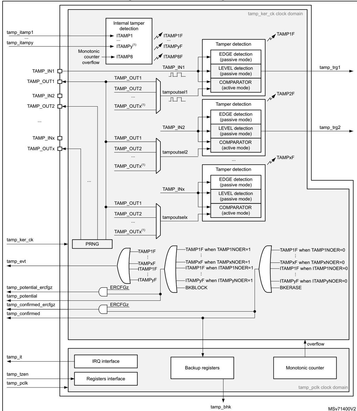
The diagram illustrates the internal architecture of the TAMP block, divided into two main clock domains: tamp_ker_ck and tamp_pclk .
- tamp_ker_ck clock domain:
- Internal tamper detection: Receives inputs from tamp_itamp1 through tamp_itampy . It includes a Monotonic counter overflow block and generates internal flags ITAMP1F , ITAMPyF , and ITAMP8F .
- External Tamper Detection: Multiple blocks (labeled Tamper detection ) process external pins TAMP_IN1 , TAMP_IN2 , and TAMP_INx . Each block contains EDGE detection (passive mode) , LEVEL detection (passive mode) , and a COMPARATOR (active mode) . These generate flags TAMP1F , TAMP2F , and TAMPxF .
- Logic and Event Generation:
- Flags TAMP1F through TAMPxF and ITAMP1F through ITAMPyF are inputs to a series of AND/OR gates.
- Control signals tamp_potential_ercfgz , tamp_potential , tamp_confirmed_ercfgz , and tamp_confirmed are also inputs to these gates.
- The final output is tamp_evt .
- PRNG: Receives input from tamp_ker_ck .
- Backup registers: Connected to the logic gates and the monotonic counter.
- Monotonic counter: Generates an overflow signal.
- tamp_pclk clock domain:
- Interfaces: Includes an IRQ interface (outputting tamp_it ) and a Registers interface (inputs: tamp_tzen , tamp_pclk ).
- Output: tamp_bhk .
MSV71400V2
1. The number of external and internal tampers depends on products.
64.4.2 TAMP pins and internal signals
Table 642. TAMP input/output pins
| Pin name | Signal type | Description |
|---|---|---|
| TAMP_INx (x = pin index) | Input | Tamper input pin |
| TAMP_OUTx (x = pin index) | Output | Tamper output pin (active mode only) |
Table 643. TAMP internal input/output signals
| Internal signal name | Signal type | Description |
|---|---|---|
| tamp_ker_ck | Input | TAMP kernel clock, connected to rtc_ker_ck and also named RTCCLK in this document |
| tamp_pclk | Input | TAMP APB clock, connected to rtc_pclk |
| tamp_itamp[y] (y = signal index) | Inputs | Internal tamper event sources |
| tamp_tzen | Input | TAMP TrustZone enabled |
| tamp_evt | Output | Tamper event detection flag (internal or external tamper), whatever confirmed or potential mode configuration. |
| tamp_potential | Output | Potential tamper detection signal, used for device secrets
(1)
protection. This signal is active when:
|
| tamp_confirmed | Output | Confirmed tamper detection signal, used for device secrets
(1)
protection. This signal is active when:
|
| tamp_potential_ercfgz (z = signal index) | Output | Potential tamper detection signal generated only when ERCFGz = 1. This signal is active when:
|
Table 643. TAMP internal input/output signals (continued)
| Internal signal name | Signal type | Description |
|---|---|---|
| tamp_confirmed_ercfgz (z = signal index) | Output | Confirmed tamper detection signal generated only when ERCFGz = 1. This signal is active when: – a tamper event detection flag (internal or external tamper), is generated in confirmed mode. – or a software request is done by writing BKERASE to 1 |
| tamp_it | Output | TAMP interrupt (refer to Section 64.6: TAMP interrupts for details) |
| tamp_trg[x] (x = signal index) | Output | Tamper detection trigger |
| tamp_bhk | Output | Tamper boot hardware key bus |
1. Refer to Table 644: TAMP interconnection .
The TAMP kernel clock is usually the LSE at 32.768 kHz although it is possible to select other clock sources in the RCC (refer to RCC for more details). The TAMP kernel clock is required only for external tamper inputs level with filtering, and for external active tamper detection modes. Internal tampers detection and external tampers inputs edge detection are functional without requiring any kernel clock.
Read and write access to backup registers and all other TAMP registers are also functional without any kernel clock (only APB clock is needed).
Some detections modes are not available in some low-power modes or V BAT depending on the selected clock (refer to for more details).
Table 644. TAMP interconnection
| Signal name | Source/Destination |
|---|---|
| tamp_tzen | From FLASH option bytes: TZEN |
| tamp_evt | rtc_tamp_evt used to generate a timestamp event |
| tamp_potential | The tamp_potential signal is used to block the read and write accesses to the device secrets listed hereafter:
RHUK (root hardware unique key) in system Flash memory and BHK (boot hardware key) hardware buses to SAES are blocked. The tamp_potential signal is used to erase the device secrets listed hereafter:
The device secrets access is blocked when erase is ongoing. |
Table 644. TAMP interconnection (continued)
| Signal name | Source/Destination |
|---|---|
| tamp_confirmed | The
The device secrets access is blocked when erase is ongoing. |
| tamp_potential_ercfg0 | When the bit ERCFG0 is set in the TAMP_ERCFGGR, the
|
| tamp_confirmed_ercfg0 | When the bit ERCFG0 is set in the TAMP_ERCFGGR, the
The device secrets access is blocked when erase is on-going. |
| tamp_itamp1 | Backup domain voltage threshold monitoring (1) |
| tamp_itamp2 | Temperature monitoring (1) |
| tamp_itamp3 | LSE monitoring (LSECSS) (2) |
| tamp_itamp5 | RTC calendar overflow (rtc_calovf) |
| tamp_itamp6 | JTAG/SWD access when RDP > 0 |
| tamp_itamp7 | ADC4 (adc4_awd1) analog watchdog monitoring 1 |
| tamp_itamp8 (3) | Monotonic counter 1 overflow |
| tamp_itamp9 | Cryptographic peripherals fault (SAES or AES or PKA or TRNG) |
| tamp_itamp11 | IWDG reset when tamper flag is set (potential tamper timeout) |
| tamp_itamp12 | ADC4 (adc4_awd2) analog watchdog monitoring 2 |
| tamp_itamp13 | ADC4 (adc4_awd3) analog watchdog monitoring 3 |
| tamp_bhk | saes_bhk
. This bus is used to load the boot hardware key in the secure AES co-processor. |
- 1. This monitoring must be enabled by setting MONEN in PWR backup domain control register 1 (PWR_BDCR1) .
- 2. This monitoring must be enabled by setting LSECSSON in RCC backup domain control register (RCC_BDCR) .
- 3. This signal is generated in the TAMP peripheral.
The TZEN option bit is used to activate TrustZone in the device.
TZEN = 1: TrustZone activated.
TZEN = 0: TrustZone disabled.
When TrustZone is disabled, the APB access to the TAMP registers are nonsecure.
64.4.3 GPIOs controlled by the RTC and TAMP
Refer to Section 63.3.3: GPIOs controlled by the RTC and TAMP .
64.4.4 TAMP register write protection
After system reset, the TAMP registers (including backup registers) are protected against parasitic write access by the DBP bit in the power control peripheral (refer to the PWR power control section). DBP bit must be set in order to enable TAMP registers write access.
64.4.5 TAMP secure protection modes
Unless otherwise specified, after a backup domain reset, all TAMP registers are readable and writable in both secure and nonsecure modes. For information about specific bitfields or complete registers that are writable only in secure mode, see Section 64.7: TAMP registers . The TAMP protection configuration is not affected by a system reset.
- • When the TAMPSEC bit is set in the TAMP_SECCFGR register:
- – Writing the TAMP registers is possible only in secure mode, except for the backup registers and monotonic counters which have their own protection setting.
- – Reading TAMP_SECCFGR, TAMP_PRIVCFGR and TAMP_MISR is always possible in secure and nonsecure modes. All the other TAMP registers can be read only in secure mode, except for the backup registers and monotonic counters which have their own protection setting.
- • When the CNT1SEC bit is set in the TAMP_SECCFGR register: the TAMP_COUNT1R can be read and written only in secure mode, and CNT1PRIV can be written only in secure mode.
A nonsecure access to a secure-protected register is denied:
- • There is no bus error generated.
- • A notification is generated through a flag/interrupt in the TZIC (TrustZone illegal access controller).
- • When write protected, the bits are not written.
- • When read protected they are read as 0.
As soon as at least one function is configured to be secured, the TAMP reset and clock control is also secured in the RCC.
64.4.6 Backup registers protection zones
The backup registers protection is configured thanks to BKPRWSEC[7:0] and BKPWSEC[7:0] (refer to the figure below):
Figure 775. Backup registers protection zones
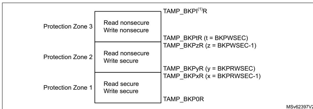
| TAMP_BKPI (1) R | ||
| Protection Zone 3 | Read nonsecure Write nonsecure | |
| TAMP_BKPrR (t = BKPWSEC) TAMP_BKPzR (z = BKPWSEC-1) | ||
| Protection Zone 2 | Read nonsecure Write secure | |
| TAMP_BKPyR (y = BKPRWSEC) TAMP_BKPxR (x = BKPRWSEC-1) | ||
| Protection Zone 1 | Read secure Write secure | |
| TAMP_BKP0R |
1. l = last backup register index
64.4.7 TAMP privilege protection modes
By default after a backup domain power-on reset, all TAMP registers can be read or written in both privileged and unprivileged modes, except for the TAMP privilege configuration register (TAMP_PRIVCFG) which can be written in privilege mode only. The TAMP protection configuration is not affected by a system reset.
- • When the TAMPPRIV bit is set in the TAMP_PRIVCFG register:
- – Writing the TAMP registers is possible only in privilege mode, except for the backup registers and the monotonic counter which have their own protection setting.
- – Reading TAMP_SECCFGR, TAMP_PRIVCFG is always possible in privilege and unprivilege modes. All the other TAMP registers can be read only in privileged mode, except for the backup registers and the monotonic counter which have their own protection setting.
- • When the CNT1PRIV bit is set in the TAMP_PRIVCFG register: the TAMP_COUNT1R can be read and written only in privilege mode, and CNT1SEC can be written only in privilege mode.
- • When the BKPRWPRIV is set in the TAMP_PRIVCFG register: the BKPWSEC can be written only in privilege mode.
- • When the BKPWPRIV is set in the TAMP_PRIVCFG register: the BKPRWSEC and BKPWSEC can be written only in privilege mode.
The backup registers protection is configured thanks to BKPRWSEC[7:0] and BKPRWPRIV for the protection zone 1, and thanks to BKPRWSEC[7:0], BKPWSEC[7:0] and BKPWPRIV for the protection zone 2 (refer to Figure 775). The BHKLOCK bit can be written only in privileged mode when the BKPRWPRIV bit is set.
A unprivileged access to a privileged-protected register is denied:
- • There is no bus error generated.
- • When write protected, the bits are not written.
- • When read protected they are read as 0.
64.4.8 Boot hardware key (BHK)
The eight first backup registers from TAMP_BKP0R to TAMP_BKP7R can be used to store a boot hardware key for the secure AES.
For this purpose, these registers must belong to the Protection Zone 1: BKPRWSEC must be greater or equal to 8.
Once the backup registers are written with the boot hardware key, the BHKLOCK bit must be set in the TAMP_SECCFGR register. Once BHKLOCK is set, the 8 backup registers cannot be accessed anymore by software: they are read as 0 and write to these registers is ignored. BHKLOCK cannot be cleared by software, and is cleared by hardware following a tamper event or when the readout protection (RDP) is disabled. It is also cleared with BKERASE command (in all cases the backup registers are also erased).
Refer to section secure AES co-processor (SAES) for details on procedure to download the boot hardware key in the SAES.
64.4.9 Tamper detection
The tamper detection main purpose is to protect the device secrets from device external attacks. The detection is made on events on TAMP_INx (x = pin index) I/Os, or on internal monitors detecting out-of-range device conditions.
The tamper detection can be configured for the following purposes:
- • erase the backup registers and other device secrets stored in SRAMs or peripherals listed in Table 644: TAMP interconnection
- • block the read/write access to the backup registers and other device secrets stored in SRAMs or peripherals listed in Table 644: TAMP interconnection
- • generate an interrupt, capable to wake-up from low-power modes
- • generate a hardware trigger for the low-power timers, or a RTC timestamp event
The external I/Os tamper detection supports 2 main configurations:
- • Passive mode: TAMP_INx I/Os are monitored and a tamper is detected either on edge or on level.
- • Active mode: TAMP_INx (x = pin index) is continuously compared with TAMP_OUTy (y = pin index) allowing open-short detection.
A digital filter can be applied on external tamper detection to avoid false detection. In addition, it is possible to configure each tamper source in potential mode, so that the secrets erase is not launched by hardware on tamper detection. The secrets erase can then be launched by software after software checks.
64.4.10 TAMP backup registers and other device secrets erase
The backup registers (TAMP_BKPxR) are not reset by system reset or when the device wakes up from Standby mode.
The backup registers and the other device secrets are not reset when the corresponding mask is set (TAMPxMSK=1 in the TAMP_CR2 register).
Note: The backup registers are also erased when the readout protection of the flash is changed from level 1 to level 0.
Tamper detection – confirmed mode
The confirmed mode is selected for TAMPx (external tamper x) when TAMPxNOER = 0 in the TAMP_CR2 register. The confirmed mode is selected for ITAMPx (internal tamper x) when ITAMPxNOER = 0 in the TAMP_CR3 register. The effects of a tamper detection in confirmed mode are described with tamp_confirmed and tamp_confirmed_ercfgx signals in the Table 644: TAMP interconnection .
This mode is selected to erase automatically the device secrets when the tamper is detected.
Tamper detection – potential mode
The potential mode is selected for TAMPx (external tamper x) when TAMPxNOER = 1 in the TAMP_CR2 register. The potential tamper mode is selected for ITAMPx (internal tamper x) when ITAMPxNOER = 1 in the TAMP_CR3 register. The effects of a tamper detection in potential mode are described with tamp_potential and tamp_potential_ercfgx signals in the Table 644: TAMP interconnection .
This mode is selected to avoid irreversible erasure of some device secrets when the tamper is detected. In this mode, some device secrets are not erased when the corresponding tamper event is detected. In addition, the read and write accesses to these device secrets are blocked as soon as the tamper detection flag is set in potential mode, until this flag is cleared by setting the corresponding clear flag in the TAMP_SCR register. Therefore the software can perform some checks to discriminate false from true tampers, and decide to launch secrets erase only in case of the potential tamper is confirmed to be a true tamper. The device secrets are erased by software by setting the BKERASE bit in the TAMP_CR2 register.
Potential tamper to confirmed tamper timeout
Some internal tampers generate a tamper event if the independent watchdog reset occurs when another tamper flag is set (refer to Table 644: TAMP interconnection ). The IWDG tamper must be configured with ITAMPxNOER = 0. This permits the erasure of device secrets to be forced by hardware after a timeout, in case the previous tamper event was in potential mode. This is equivalent to change the “potential tamper” into “confirmed tamper” if a watchdog reset occurs before any software decision following the potential tamper event.
Device resources protection configuration
Some device resources can be configured in order to be included to the list of the device secrets protected by tamper detection.
When ERCFGz = 0 in the TAMP_ERCFGR, the device resource associated to ERCFGz is not protected by the TAMP peripheral:
- • It is not affected by tamper detection (whatever confirmed or potential mode)
- • It is not affected by BKERASE software command
- • It is not affected by BKBLOCK software command
When ERCFGz = 1 in the TAMP_ERCFGR, the device resource associated to ERCFGz is protected by the TAMP peripheral:
- • It is affected by confirmed tamper detection and BKERASE software command, as described with tamp_confirmed_ercfgz signal in Table 644: TAMP interconnection
- • It is affected by potential tamper detection and BKBLOCK software command, as described with tamp_potential_ercfgz signal in Table 644: TAMP interconnection
| - | Potential tamper or BKBLOCK | Confirmed tamper or BKERASE |
|---|---|---|
| RPCFGx = 0 | No effect on device resource x | No effect on device resource x |
| RPCFGx = 1 | Device secret x protected as described by
tamp_potential_ercfgx
(1) | Device secret x protected as described by
tamp_confirmed_ercfgx
(1) |
1. Refer to Table 644: TAMP interconnection .
Device secrets access blocked by software
By default, the device secrets can be accessed by the application, except if a tamper event flag is detected: the device secrets access is not possible as long as a tamper flag is set.
It is possible to block the access to the device secrets by software, by setting the BKBLOCK bit of the TAMP_CR2 register. The device secrets access is possible only when BKBLOCK = 0 and no tamper flag is set.
64.4.11 Tamper detection configuration and initialization
Each input can be enabled by setting the corresponding TAMPxE bits to 1 in the TAMP_CR register.
Each TAMP_INx tamper detection input is associated with a flag TAMPxF in the TAMP_SR register.
By setting the TAMPxIE bit in the TAMP_IER register, an interrupt is generated when a tamper detection event occurs (when TAMPxF is set). Setting TAMPxIE is not allowed when the corresponding TAMPxMSK is set.
Trigger output generation on tamper event
The tamper event detection can be used as trigger input by the low-power timers.
When TAMPxMSK bit is cleared in TAMP_CR register, the TAMPxF flag must be cleared by software in order to allow a new tamper detection on the same pin.
When TAMPxMSK bit is set, the TAMPxF flag is masked, and kept cleared in TAMP_SR register. This configuration permits the low-power timers to be triggered automatically in Stop mode, without requiring the system wake-up to perform the TAMPxF clearing. In this case, the backup registers are not cleared.
This feature is available only when the tamper is configured in level detection with filtering mode (
TAMPFLT
≠ 00 and active mode is not selected). Refer to
Section : Level detection with filtering on tamper inputs (passive mode)
.
Timestamp on tamper event
With TAMPTS set to 1 in the RTC_CR, any internal or external tamper event causes a timestamp to occur. In case a timestamp occurs due to tamper event, either the TSF bit or the TSOVF bit is set in RTC_SR, in the same manner as if a normal timestamp event occurs.
Note: TSF is set up to 3 ck_apre cycles after TAMPxF flags. TSF is not set if RTCCLK is stopped (it is set when RTCCLK restarts).
Note: If TAMPxF is cleared before the expected rise of TSF, TSF is not set. Consequently, in case TAMPTS = 1, the software should either wait for timestamp flag before clearing the tamper flag, or should read the RTC counters values in the TAMP interrupt routine.
Edge detection on tamper inputs (passive mode)
If the TAMPFLT bits are 00, the TAMP_INx pins generate tamper detection events when either a rising edge or a falling edge is observed depending on the corresponding TAMPxTRG bit. The internal pull-up resistors on the TAMP_INx inputs are deactivated when edge detection is selected.
Caution: When TAMPFLT = 00 and TAMPxTRG = 0 (rising edge detection), a tamper event may be detected by hardware if the tamper input is already at high level before enabling the tamper detection.
After a tamper event has been detected and cleared, the TAMP_INx should be disabled and then re-enabled (TAMPxE set to 1) before re-programming the backup registers (TAMP_BKPxR). This prevents the application from writing to the backup registers while the TAMP_INx input value still indicates a tamper detection. This is equivalent to a level detection on the TAMP_INx input.
Note: Tamper detection is still active when V DD power is switched off. To avoid unwanted resetting of the backup registers, the pin to which the TAMPx is mapped should be externally tied to the correct level.
Level detection with filtering on tamper inputs (passive mode)
Level detection with filtering is performed by setting TAMPFLT to a non-zero value. A tamper detection event is generated when either 2, 4, or 8 (depending on TAMPFLT) consecutive samples are observed at the level designated by the TAMPxTRG bits.
The TAMP_INx inputs are precharged through the I/O internal pull-up resistance before its state is sampled, unless disabled by setting TAMPPUDIS to 1. The duration of the precharge is determined by the TAMPPRCH bits, allowing for larger capacitances on the TAMP_INx inputs.
The trade-off between tamper detection latency and power consumption through the pull-up can be optimized by using TAMPFREQ to determine the frequency of the sampling for level detection. The TAMP_IN I/O schmitt trigger is enabled only during the precharge duration to avoid any extra consumption if the tamper switch is open (floating state).
Figure 776. Tamper sampling with precharge pulse
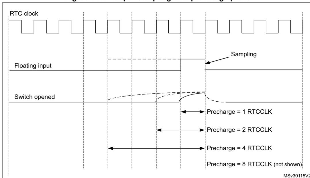
Figure 776 shows the timing for tamper sampling with a precharge pulse. The top waveform is the RTC clock. The middle waveform is the Floating input, which is sampled at regular intervals. The bottom waveform is the Switch opened signal. The diagram indicates the sampling period and the precharge duration, which is shown for 1, 2, 4, and 8 RTCCLK cycles. The 8-cycle duration is not shown.
MSv30115V2
Figure 777. Low level detection with precharge and filtering
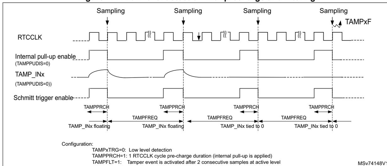
Figure 777 shows the timing for low level detection with precharge and filtering. The top waveform is the RTCCLK. The second waveform is the Internal pull-up enable (TAMPPUDIS=0), which is high during sampling. The third waveform is the TAMP_INx (TAMPPUDIS=0), which is high when the internal pull-up is enabled. The bottom waveform is the Schmitt trigger enable. The diagram shows the sampling process and the duration of the precharge pulse (TAMPPRCH) and the filtering period (TAMPFREQ). The configuration is set for low level detection with 1 RTCCLK cycle pre-charge duration and 2 consecutive samples at active level.
Configuration:
TAMPxTRG=0: Low level detection
TAMPPRCH=1: 1 RTCCLK cycle pre-charge duration (internal pull-up is applied)
TAMPFLT=1: Tamper event is activated after 2 consecutive samples at active level
MSv74148V1
Note: Refer to the microcontroller datasheet for the electrical characteristics of the pull-up resistors.
Active tamper detection
When the TAMPxAM bit is set in the TAMP_ATCR, the tamper events are configured in active mode, which is based on a comparison between a TAMP_OUTy pin and a TAMP_INx pin. By default (ATOSHARE = 0) the comparison is made between TAMP_INx and TAMP_OUTx (y = x). When ATOSHARE bit is set, the same output can be used for several tamper inputs. The TAMP_OUTy function is enabled on the I/O as soon as it is selected for comparison with an active tamper input TAMP_INx (TAMPxEN = TAMPxAM = 1), thanks to
ATOSHARE and ATOSELx bits. Refer to ATOSHARE and ATOSEL bits descriptions in the TAMP_ATCRx (x = 1, 2) registers.
Every two CK_ATPER cycles ( \( CK\_ATPER = 2^{ATPER} \times CK\_ATPRE \) ), TAMP_OUTy output pin provides a value provided by a pseudo random number generator (PRNG). After outputting this value, the TAMP_OUTy pin outputs its opposite value one CK_ATPER cycle after.
Table 646. Active tamper output change period
| ATCKSEL[3:0] | CK_ATPRE frequency | ATPER[2:0] | Tamper output change (CK_ATPER) frequency | Tamper output change period (1) (ms) |
|---|---|---|---|---|
| 0x0 | \( f_{RTCCLK} \) | 0x0 | \( f_{RTCCLK} \) | 0.030 |
| 0x1 | \( f_{RTCCLK}/2 \) | 0.061 | ||
| 0x2 | \( f_{RTCCLK}/4 \) | 0.122 | ||
| 0x3 | \( f_{RTCCLK}/8 \) | 0.244 | ||
| 0x4 | \( f_{RTCCLK}/16 \) | 0.488 | ||
| 0x5 | \( f_{RTCCLK}/32 \) | 0.977 | ||
| 0x6 | \( f_{RTCCLK}/64 \) | 1.953 | ||
| 0x7 | \( f_{RTCCLK}/128 \) | 3.906 | ||
| ... | ... | ... | ... | ... |
| 0x7 | \( f_{RTCCLK}/128 \) | 0x0 | \( f_{RTCCLK}/128 \) | 3.906 |
| 0x1 | \( f_{RTCCLK}/256 \) | 7.8125 | ||
| 0x2 | \( f_{RTCCLK}/512 \) | 15.625 | ||
| 0x3 | \( f_{RTCCLK}/1024 \) | 31.250 | ||
| 0x4 | \( f_{RTCCLK}/2048 \) | 62.5 | ||
| 0x5 | \( f_{RTCCLK}/4096 \) | 125 | ||
| 0x6 | \( f_{RTCCLK}/8192 \) | 250 | ||
| 0x7 | \( f_{RTCCLK}/16384 \) | 500 | ||
| 0xB (2) | \( f_{RTCCLK}/2048^{(3)} \) | 0x0 | \( f_{RTCCLK}/2048 \) | 62.5 |
| 0x1 | \( f_{RTCCLK}/4096 \) | 125 | ||
| 0x2 | \( f_{RTCCLK}/8192 \) | 250 | ||
| 0x3 | \( f_{RTCCLK}/16384 \) | 500 | ||
| 0x4 | \( f_{RTCCLK}/32768 \) | 1000 | ||
| 0x5 | \( f_{RTCCLK}/65536 \) | 2000 | ||
| 0x6 | \( f_{RTCCLK}/131072 \) | 4000 | ||
| 0x7 | \( f_{RTCCLK}/262144 \) | 8000 |
- 1. Assuming \( f_{RTCCLK} = 32768 \) Hz.
- 2. These values are supported only when the active tamper prescaler extension is supported. Refer to Section 64.3: TAMP implementation .
- 3. This setting requires that (PREDIV_A+1) = 128 and (PREDIV_S+1) is a multiple of 16.
PRNG is consumed by the selected tamper outputs at a different frequency depending on the number of selected tamper outputs. The number of selected outputs depends on TAMPxAM, TAMPxE, ATOSEL and ATOSHARE.
- • When only 1 output is selected: PRNG is consumed every 16 CK_ATPER periods.
- • When 2 outputs are selected: PRNG is consumed every 8 CK_ATPER periods.
- • When 3 or 4 outputs are selected: PRNG is consumed every 4 CK_ATPER periods.
- • When 5 or more outputs are selected: PRNG is consumed every 2 CK_ATPER periods.
The PRNG needs minimum 9 CK_ATPRE cycles to output a new value. Consequently the minimum ATPER values for correct functionality are provided in the table below:
Table 647. Minimum ATPER value
| Number of selected outputs | Minimum ATPER |
|---|---|
| 1 | 0 |
| 2 | 1 |
| 3 or 4 | 2 |
| 5 or more | 3 |
The TAMP_INx pin is externally connected to TAMP_OUTy pin. The comparison is made between TAMP_OUTy output value and TAMP_INx received value, every CK_ATPRE cycle. In case a comparison mismatch occurs, the TAMPxF bit is set in the TAMP_SR register.
As an example, TAMP_OUT1 can be used for comparison with TAMP_IN1 and TAMP_IN2 by configuring and enabling both TAMP1 and TAMP2 in active mode, with ATOSHARE = 1, ATOSEL1 = 000 and ATOSEL2 = 000.
The active tamper can be combined with input filtering when FLTEN = 1. In this case, the tamper is detected only when 2 comparisons are false, in 4 consecutive comparison samples.
Figure 778. Active tamper filtering
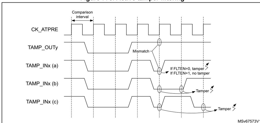
The diagram illustrates the timing for active tamper filtering. The top waveform is the CK_ATPRE clock. Below it is the TAMP_OUTy signal. The next three are input signals: TAMP_INx (a) , TAMP_INx (b) , and TAMP_INx (c) . Vertical dashed lines mark the Comparison interval for each clock cycle. A 'Mismatch' is shown between TAMP_OUTy and TAMP_INx (a). A legend indicates: 'If FLTEN=0, tamper' and 'If FLTEN=1, no tamper'. Arrows point to tamper events on TAMP_INx (b) and TAMP_INx (c). The code MSV67573V1 is shown in the bottom right corner.
As illustrated in Figure 778 , if FLTEN = 0, any mismatch between the TAMP_OUTy output and the associated TAMP_INx input when the latter is sampled generates a tamper. This is the case in all three examples (a), (b) and (c).
If FLTEN = 1, example (a) does not generate a tamper, since only one mismatch is detected in four consecutive comparisons. In example (b), a tamper is generated since two successive mismatches are detected. Example (c) also generates a tamper, since two mismatches occur in four consecutive comparisons, even though the mismatches do not occur on successive samples.
Setting FLTEN = 1 avoids unwanted detection of tampers due to glitches, bounce or transitory states on the TAMP_INx inputs, by ignoring single pulses which are shorter than one period of CK_ATPRE, programmed in the ATCKSEL field of the TAMP_ATCR1 register. The minimum filtered pulse width is listed in Table 648 for each possible setting of ATCKSEL, assuming \( f_{RTCCLK} = 32.768 \) kHz.
Table 648. Active tamper filtered pulse duration
| ATCKSEL[3:0] | CK_ATPRE frequency | Minimum filtered pulse width (ms) |
|---|---|---|
| 0x0 | \( f_{RTCCLK} \) | 0.030 |
| 0x1 | \( f_{RTCCLK}/2 \) | 0.061 |
| 0x2 | \( f_{RTCCLK}/4 \) | 0.122 |
| 0x3 | \( f_{RTCCLK}/8 \) | 0.244 |
| 0x4 | \( f_{RTCCLK}/16 \) | 0.488 |
| 0x5 | \( f_{RTCCLK}/32 \) | 0.977 |
| 0x6 | \( f_{RTCCLK}/64 \) | 1.953 |
| 0x7 | \( f_{RTCCLK}/128 \) | 3.906 |
| 0xB (1) | \( f_{RTCCLK}/2048 \) | 62.500 (2) |
1. These values are supported only when the active tamper prescaler extension is supported. Refer to Section 64.3: TAMP implementation .
2. This setting requires that (PREDIV_A+1) = 128 and (PREDIV_S+1) is a multiple of 16.
Note: Multiple pulses which are shorter than one CK_ATPRE period may nevertheless cause a tamper if they result in two mismatches in four consecutive comparisons.
Caution: Entering RTC initialization mode stops CK_ATPRE and CK_ATPER clocks when ATCKSEL[3] = 1. Therefore, TAMP_OUTy pin stops toggling until INIT mode exit.
Refer to section Section : Calendar initialization and configuration .
Refer also to RTC alarm A subsecond register (RTC_ALRMASSR) , RTC alarm B subsecond register (RTC_ALRMBSSR) , RTC alarm A binary mode register (RTC_ALRABINR) and RTC alarm B binary mode register (RTC_ALRBBINR) in case RTC binary mode is used in conjunction with ATCKSEL[3] = 1.
Caution: The active tamper detection is no more functional in case of calendar overflow when ATCKSEL[3] = 1. It is mandatory to enable the internal tamper 5 on calendar overflow to ensure tamper protection.
The pseudo-random generator must be initialized with a seed. This is done by writing consecutively four 32-bit random values in the TAMP_ATSEEDR register. Programming the seed automatically sends it to the PRNG. As long as the new seed is transferred and
elaborated by the PRNG, the SEEDF bit is set in the TAMP_ATOR and it is not allowed to switch off the TAMP APB clock. The duration of the elaboration is up to 184 APB clock cycles after the forth seed is written. Consequently, after writing a new seed, the user must wait until SEEDF is cleared before entering low-power modes.
The active tamper outputs are activated only after the first seed is written and the elaboration is completed. Then new seeds can be written and elaborated during active tamper activity.
Active tamper initialization
Here is the software procedure to initialize the active tampers after system reset:
Read INITS in TAMP_ATOR register.
- • If INITS = 0x0 (initialization was not done):
- a) Write TAMP_ATCR to configure Active tamper clock, filter and output sharing if any, and active mode.
- b) Write TAMP_CR1 to enable tampers (all the needed tampers must be enabled in the same write access).
- c) Write SEED by writing four times in the TAMP_ATSEEDR.
- d) Wait until SEEDF = 0 in TAMP_ATOR. Backup registers are then protected by active tamper.
- • If INITS = 0x1 (initialization already done):
No initialization. To increase randomness a new SEED should be provided regularly. When a new SEED is provided, wait until SEEDF = 0 before entering a low-power mode which switches off the TAMP APB clock.
- • In case the tampers are disabled by software, and re-enabled afterwards, the SEED must be written after enabling tampers:
- a) Write TAMP_CR1 to enable tampers (all the needed tampers must be enabled in the same write access).
- b) Write SEED by writing four times in the TAMP_ATSEEDR.
- c) Wait until SEEDF = 0 in TAMP_ATOR. Backup registers are then protected by active tamper.
64.5 TAMP low-power modes
Table 649. Effect of low-power modes on TAMP
| Mode | Description |
|---|---|
| Sleep | No effect. TAMP interrupts cause the device to exit the Sleep mode. |
| Stop | No effect, except for level detection with filtering and active tamper modes which remain active only when the clock source is LSE or LSI. Some internal tampers sources are not functional, refer to
Table 100: Functionalities depending on the working mode
. TAMP interrupts cause the device to exit the Stop mode. |
| Standby | No effect, except for level detection with filtering and active tamper modes which remain active only when the clock source is LSE or LSI. Some internal tampers sources are not functional, refer to
Table 100: Functionalities depending on the working mode
. TAMP interrupts cause the device to exit the Standby mode. |
| Shutdown | No effect, except for level detection with filtering and active tamper modes which remain active only when the clock source is LSE. Some internal tampers sources are not functional, refer to
Table 100: Functionalities depending on the working mode
. TAMP interrupts cause the device to exit the Shutdown mode. |
Table 650. TAMP pins functionality over modes
| Pin name | Functional in all low-power modes | Functional in V BAT mode |
|---|---|---|
| TAMP_IN[8:1] | Yes | Yes |
| TAMP_OUT[8:1] | Yes | Yes |
64.6 TAMP interrupts
The interrupt channel is set in the masked interrupt status register or in the secure masked interrupt status register depending on its security mode configuration (TAMPSEC).
Table 651. Interrupt requests
| Interrupt acronym | Interrupt event | Event flag (1) | Enable control bit | Interrupt clear method | Exit from low-power modes |
|---|---|---|---|---|---|
| TAMP | Tamper x (2) | TAMPxF | TAMPxIE | Write 1 in CTAMPxF | Yes (3) |
| Internal tamper y (2) | ITAMPyF | ITAMPyIE | Write 1 in CITAMPyF | Yes (3) |
- 1. The event flags are in the TAMP_SR register.
- 2. The number of tampers and internal tampers events depend on products.
- 3. Refer to Table 649: Effect of low-power modes on TAMP for more details about available features in the low-power modes.
64.7 TAMP registers
Refer to Section 1.2 of the reference manual for a list of abbreviations used in register descriptions. The peripheral registers can be accessed by words (32-bit).
64.7.1 TAMP control register 1 (TAMP_CR1)
This register can be protected against nonsecure access. Refer to Section 64.4.5: TAMP secure protection modes .
This register can be protected against unprivileged access. Refer to Section 64.4.7: TAMP privilege protection modes .
Address offset: 0x00
Backup domain reset value: 0x0000 0000
System reset: not affected
| 31 | 30 | 29 | 28 | 27 | 26 | 25 | 24 | 23 | 22 | 21 | 20 | 19 | 18 | 17 | 16 |
|---|---|---|---|---|---|---|---|---|---|---|---|---|---|---|---|
| Res. | Res. | Res. | ITAMP13E | ITAMP12E | ITAMP11E | Res. | ITA-MP9E | ITAMP8E | ITA-MP7E | ITAMP6E | ITAMP5E | Res. | ITAMP3E | ITAMP2E | ITAMP1E |
| rw | rw | rw | rw | rw | rw | rw | rw | rw | rw | rw | |||||
| 15 | 14 | 13 | 12 | 11 | 10 | 9 | 8 | 7 | 6 | 5 | 4 | 3 | 2 | 1 | 0 |
| Res. | Res. | Res. | Res. | Res. | Res. | Res. | Res. | TAMP8E | TAMP7E | TAMP6E | TAMP5E | TAMP4E | TAMP3E | TAMP2E | TAMP1E |
| rw | rw | rw | rw | rw | rw | rw | rw |
Bit 31 Reserved, must be kept at reset value.
Bit 30 Reserved, must be kept at reset value.
Bit 29 Reserved, must be kept at reset value.
Bit 28 ITAMP13E : Internal tamper 13 enable
0: Internal tamper 13 disabled.
1: Internal tamper 13 enabled.
Bit 27 ITAMP12E : Internal tamper 12 enable
0: Internal tamper 12 disabled.
1: Internal tamper 12 enabled.
Bit 26 ITAMP11E : Internal tamper 11 enable
0: Internal tamper 11 disabled.
1: Internal tamper 11 enabled.
Bit 25 Reserved, must be kept at reset value.
Bit 24 ITAMP9E : Internal tamper 9 enable
0: Internal tamper 9 disabled.
1: Internal tamper 9 enabled.
Bit 23 ITAMP8E : Internal tamper 8 enable
0: Internal tamper 8 disabled.
1: Internal tamper 8 enabled.
Bit 22 ITAMP7E : Internal tamper 7 enable
0: Internal tamper 7 disabled.
1: Internal tamper 7 enabled
- Bit 21
ITAMP6E
: Internal tamper 6 enable
0: Internal tamper 6 disabled.
1: Internal tamper 6 enabled. - Bit 20
ITAMP5E
: Internal tamper 5 enable
0: Internal tamper 5 disabled.
1: Internal tamper 5 enabled. - Bit 19 Reserved, must be kept at reset value.
- Bit 18
ITAMP3E
: Internal tamper 3 enable
0: Internal tamper 3 disabled.
1: Internal tamper 3 enabled. - Bit 17
ITAMP2E
: Internal tamper 2 enable
0: Internal tamper 2 disabled.
1: Internal tamper 2 enabled. - Bit 16
ITAMP1E
: Internal tamper 1 enable
0: Internal tamper 1 disabled.
1: Internal tamper 1 enabled. - Bits 15:8 Reserved, must be kept at reset value.
- Bit 7
TAMP8E
: Tamper detection on TAMP_IN8 enable
(1)
0: Tamper detection on TAMP_IN8 is disabled.
1: Tamper detection on TAMP_IN8 is enabled. - Bit 6
TAMP7E
: Tamper detection on TAMP_IN7 enable
(1)
0: Tamper detection on TAMP_IN7 is disabled.
1: Tamper detection on TAMP_IN7 is enabled. - Bit 5
TAMP6E
: Tamper detection on TAMP_IN6 enable
(1)
0: Tamper detection on TAMP_IN6 is disabled.
1: Tamper detection on TAMP_IN6 is enabled. - Bit 4
TAMP5E
: Tamper detection on TAMP_IN5 enable
(1)
0: Tamper detection on TAMP_IN5 is disabled.
1: Tamper detection on TAMP_IN5 is enabled. - Bit 3
TAMP4E
: Tamper detection on TAMP_IN4 enable
(1)
0: Tamper detection on TAMP_IN4 is disabled.
1: Tamper detection on TAMP_IN4 is enabled. - Bit 2
TAMP3E
: Tamper detection on TAMP_IN3 enable
(1)
0: Tamper detection on TAMP_IN3 is disabled.
1: Tamper detection on TAMP_IN3 is enabled. - Bit 1
TAMP2E
: Tamper detection on TAMP_IN2 enable
(1)
0: Tamper detection on TAMP_IN2 is disabled.
1: Tamper detection on TAMP_IN2 is enabled. - Bit 0
TAMP1E
: Tamper detection on TAMP_IN1 enable
(1)
0: Tamper detection on TAMP_IN1 is disabled.
1: Tamper detection on TAMP_IN1 is enabled.
- 1. Tamper detection mode (selected with TAMP_FLTCR, TAMP_ATCR1, TAMP_ATCR2 registers and TAMPxTRG bits in TAMP_CR2), must be configured before enabling the tamper detection.
64.7.2 TAMP control register 2 (TAMP_CR2)
This register can be protected against nonsecure access. Refer to Section 64.4.5: TAMP secure protection modes .
This register can be protected against unprivileged access. Refer to Section 64.4.7: TAMP privilege protection modes .
Address offset: 0x04
Backup domain reset value: 0x0000 0000
System reset: not affected
| 31 | 30 | 29 | 28 | 27 | 26 | 25 | 24 | 23 | 22 | 21 | 20 | 19 | 18 | 17 | 16 |
|---|---|---|---|---|---|---|---|---|---|---|---|---|---|---|---|
| TAMP8 TRG | TAMP7 TRG | TAMP6 TRG | TAMP5 TRG | TAMP4 TRG | TAMP3 TRG | TAMP2 TRG | TAMP1 TRG | BK ERASE | BK BLOCK | Res. | Res. | Res. | TAMP3 MSK | TAMP2 MSK | TAMP1 MSK |
| rw | rw | rw | rw | rw | rw | rw | rw | w | rw | rw | rw | rw | |||
| 15 | 14 | 13 | 12 | 11 | 10 | 9 | 8 | 7 | 6 | 5 | 4 | 3 | 2 | 1 | 0 |
| Res. | Res. | Res. | Res. | Res. | Res. | Res. | Res. | TAMP8 NOER | TAMP7 NOER | TAMP6 NOER | TAMP5 NOER | TAMP4 NOER | TAMP3 NOER | TAMP2 NOER | TAMP1 NOER |
| rw | rw | rw | rw | rw | rw | rw | rw |
Bit 31 TAMP8TRG : Active level for tamper 8 input (active mode disabled)
- 0: If TAMPFLT
\(
\neq
\)
00 tamper 8 input staying low triggers a tamper detection event.
If TAMPFLT = 00 tamper 8 input rising edge triggers a tamper detection event. - 1: If TAMPFLT
\(
\neq
\)
00 tamper 8 input staying high triggers a tamper detection event.
If TAMPFLT = 00 tamper 8 input falling edge triggers a tamper detection event.
Bit 30 TAMP7TRG : Active level for tamper 7 input (active mode disabled)
- 0: If TAMPFLT
\(
\neq
\)
00 tamper 7 input staying low triggers a tamper detection event.
If TAMPFLT = 00 tamper 7 input rising edge triggers a tamper detection event. - 1: If TAMPFLT
\(
\neq
\)
00 tamper 7 input staying high triggers a tamper detection event.
If TAMPFLT = 00 tamper 7 input falling edge triggers a tamper detection event.
Bit 29 TAMP6TRG : Active level for tamper 6 input (active mode disabled)
- 0: If TAMPFLT
\(
\neq
\)
00 tamper 6 input staying low triggers a tamper detection event.
If TAMPFLT = 00 tamper 6 input rising edge triggers a tamper detection event. - 1: If TAMPFLT
\(
\neq
\)
00 tamper 6 input staying high triggers a tamper detection event.
If TAMPFLT = 00 tamper 6 input falling edge triggers a tamper detection event.
Bit 28 TAMP5TRG : Active level for tamper 5 input (active mode disabled)
- 0: If TAMPFLT
\(
\neq
\)
00 tamper 5 input staying low triggers a tamper detection event.
If TAMPFLT = 00 tamper 5 input rising edge triggers a tamper detection event. - 1: If TAMPFLT
\(
\neq
\)
00 tamper 5 input staying high triggers a tamper detection event.
If TAMPFLT = 00 tamper 5 input falling edge triggers a tamper detection event.
Bit 27 TAMP4TRG : Active level for tamper 4 input (active mode disabled)
- 0: If TAMPFLT
\(
\neq
\)
00 tamper 4 input staying low triggers a tamper detection event.
If TAMPFLT = 00 tamper 4 input rising edge triggers a tamper detection event. - 1: If TAMPFLT
\(
\neq
\)
00 tamper 4 input staying high triggers a tamper detection event.
If TAMPFLT = 00 tamper 4 input falling edge triggers a tamper detection event.
Bit 26 TAMP3TRG : Active level for tamper 3 input
- 0: If TAMPFLT ≠ 00 tamper 3 input staying low triggers a tamper detection event.
If TAMPFLT = 00 tamper 3 input rising edge triggers a tamper detection event. - 1: If TAMPFLT ≠ 00 tamper 3 input staying high triggers a tamper detection event.
If TAMPFLT = 00 tamper 3 input falling edge triggers a tamper detection event.
Bit 25 TAMP2TRG : Active level for tamper 2 input
- 0: If TAMPFLT ≠ 00 tamper 2 input staying low triggers a tamper detection event.
If TAMPFLT = 00 tamper 2 input rising edge triggers a tamper detection event. - 1: If TAMPFLT ≠ 00 tamper 2 input staying high triggers a tamper detection event.
If TAMPFLT = 00 tamper 2 input falling edge triggers a tamper detection event.
Bit 24 TAMP1TRG : Active level for tamper 1 input
- 0: If TAMPFLT ≠ 00 tamper 1 input staying low triggers a tamper detection event.
If TAMPFLT = 00 tamper 1 input rising edge triggers a tamper detection event. - 1: If TAMPFLT ≠ 00 tamper 1 input staying high triggers a tamper detection event.
If TAMPFLT = 00 tamper 1 input falling edge triggers a tamper detection event.
Bit 23 BKERASE : Backup registers and device secrets (1) erase
Writing '1' to this bit reset the backup registers and device secrets (1) . Writing 0 has no effect. This bit is always read as 0.
Bit 22 BKBLOCK : Backup registers and device secrets (1) access blocked
- 0: backup registers and device secrets (1) can be accessed if no tamper flag is set
- 1: backup registers and device secrets (1) cannot be accessed
Bits 21:19 Reserved, must be kept at reset value.
Bit 18 TAMP3MSK : Tamper 3 mask
- 0: Tamper 3 event generates a trigger event and TAMP3F must be cleared by software to allow next tamper event detection.
- 1: Tamper 3 event generates a trigger event. TAMP3F is masked and internally cleared by hardware. The backup registers and device secrets
(1)
are not erased.
The tamper 3 interrupt must not be enabled when TAMP3MSK is set.
Bit 17 TAMP2MSK : Tamper 2 mask
- 0: Tamper 2 event generates a trigger event and TAMP2F must be cleared by software to allow next tamper event detection.
- 1: Tamper 2 event generates a trigger event. TAMP2F is masked and internally cleared by hardware. The backup registers and device secrets
(1)
are not erased.
The tamper 2 interrupt must not be enabled when TAMP2MSK is set.
Bit 16 TAMP1MSK : Tamper 1 mask
- 0: Tamper 1 event generates a trigger event and TAMP1F must be cleared by software to allow next tamper event detection.
- 1: Tamper 1 event generates a trigger event. TAMP1F is masked and internally cleared by hardware. The backup registers and device secrets
(1)
are not erased.
The tamper 1 interrupt must not be enabled when TAMP1MSK is set.
Bits 15:8 Reserved, must be kept at reset value.
Bit 7 TAMP8NOER : Tamper 8 no erase
- 0: Tamper 8 event detection is in confirmed mode (1) .
- 1: Tamper 8 event detection is in potential mode (2) .
Bit 6 TAMP7NOER : Tamper 7 no erase
- 0: Tamper 7 event detection is in confirmed mode (1) .
- 1: Tamper 7 event detection is in potential mode (2) .
Bit 5 TAMP6NOER : Tamper 6 no erase
- 0: Tamper 6 event detection is in confirmed mode (1) .
- 1: Tamper 6 event detection is in potential mode (2) .
Bit 4 TAMP5NOER : Tamper 5 no erase
- 0: Tamper 5 event detection is in confirmed mode (1) .
- 1: Tamper 5 event detection is in potential mode (2) .
Bit 3 TAMP4NOER : Tamper 4 no erase
- 0: Tamper 4 event detection is in confirmed mode (1) .
- 1: Tamper 4 event detection is in potential mode (2) .
Bit 2 TAMP3NOER : Tamper 3 no erase
- 0: Tamper 3 event detection is in confirmed mode (1) .
- 1: Tamper 3 event detection is in potential mode (2) .
Bit 1 TAMP2NOER : Tamper 2 no erase
- 0: Tamper 2 event detection is in confirmed mode (1) .
- 1: Tamper 2 event detection is in potential mode (2) .
Bit 0 TAMP1NOER : Tamper 1 no erase
- 0: Tamper 1 event detection is in confirmed mode (1) .
- 1: Tamper 1 event detection is in potential mode (2) .
- 1. The effects of tamper detection in confirmed mode is described with
tamp_confirmedandtamp_confirmed_ercfgxsignals in Table 644: TAMP interconnection . - 2. The effects of tamper detection in potential mode is described with
tamp_potentialandtamp_potential_ercfgxsignals in Table 644: TAMP interconnection .
64.7.3 TAMP control register 3 (TAMP_CR3)
This register can be protected against nonsecure access. Refer to Section 64.4.5: TAMP secure protection modes .
This register can be protected against unprivileged access. Refer to Section 64.4.7: TAMP privilege protection modes .
Address offset: 0x08
Backup domain reset value: 0x0000 0000
System reset: not affected
| 31 | 30 | 29 | 28 | 27 | 26 | 25 | 24 | 23 | 22 | 21 | 20 | 19 | 18 | 17 | 16 |
|---|---|---|---|---|---|---|---|---|---|---|---|---|---|---|---|
| Res. | Res. | Res. | Res. | Res. | Res. | Res. | Res. | Res. | Res. | Res. | Res. | Res. | Res. | Res. | Res. |
| 15 | 14 | 13 | 12 | 11 | 10 | 9 | 8 | 7 | 6 | 5 | 4 | 3 | 2 | 1 | 0 |
| Res. | Res. | Res. | ITAMP13NOE R | ITAMP12NOE R | ITAMP11NOE R | Res. | ITAMP9 NOER | ITAMP8 NOER | ITAMP7 NOER | ITAMP6 NOER | ITAMP5 NOER | Res. | ITAMP3 NOER | ITAMP2 NOER | ITAMP1 NOER |
| rw | rw | rw | rw | rw | rw | rw | rw | rw | rw | rw |
Bits 31:16 Reserved, must be kept at reset value.
Bit 15 Reserved, must be kept at reset value.
Bit 14 Reserved, must be kept at reset value.
Bit 13 Reserved, must be kept at reset value.
- Bit 12
ITAMP13NOER
: Internal tamper 13 no erase
0: Internal tamper 13 event detection is in confirmed mode (1) .
1: Internal tamper 13 event detection is in potential mode (2) . - Bit 11
ITAMP12NOER
: Internal tamper 12 no erase
0: Internal tamper 12 event detection is in confirmed mode (1) .
1: Internal tamper 12 event detection is in potential mode (2) . - Bit 10
ITAMP11NOER
: Internal tamper 11 no erase
0: Internal tamper 11 event detection is in confirmed mode (1) .
1: Internal tamper 11 event detection is in potential mode (2) . - Bit 9 Reserved, must be kept at reset value.
- Bit 8
ITAMP9NOER
: Internal tamper 9 no erase
0: Internal tamper 9 event detection is in confirmed mode (1) .
1: Internal tamper 9 event detection is in potential mode (2) . - Bit 7
ITAMP8NOER
: Internal tamper 8 no erase
0: Internal tamper 8 event detection is in confirmed mode (1) .
1: Internal tamper 8 event detection is in potential mode (2) . - Bit 6
ITAMP7NOER
: Internal tamper 7 no erase
0: Internal tamper 7 event detection is in confirmed mode (1) .
1: Internal tamper 7 event detection is in potential mode (2) . - Bit 5
ITAMP6NOER
: Internal tamper 6 no erase
0: Internal tamper 6 event detection is in confirmed mode (1) .
1: Internal tamper 6 event detection is in potential mode (2) . - Bit 4
ITAMP5NOER
: Internal tamper 5 no erase
0: Internal tamper 5 event detection is in confirmed mode (1) .
1: Internal tamper 5 event detection is in potential mode (2) . - Bit 3 Reserved, must be kept at reset value.
- Bit 2
ITAMP3NOER
: Internal tamper 3 no erase
0: Internal tamper 3 event detection is in confirmed mode (1) .
1: Internal tamper 3 event detection is in potential mode (2) . - Bit 1
ITAMP2NOER
: Internal tamper 2 no erase
0: Internal tamper 2 event detection is in confirmed mode (1) .
1: Internal tamper 2 event detection is in potential mode (2) . - Bit 0
ITAMP1NOER
: Internal tamper 1 no erase
0: Internal tamper 1 event detection is in confirmed mode (1) .
1: Internal tamper 1 event detection is in potential mode (2) .
- 1. The effects of internal tamper detection in confirmed mode is described with
tamp_confirmedandtamp_confirmed_ercfgxsignals in Table 644: TAMP interconnection - 2. The effects of internal tamper detection in potential mode is described with
tamp_potentialandtamp_potential_ercfgxsignals in Table 644: TAMP interconnection .
64.7.4 TAMP filter control register (TAMP_FLTCR)
This register can be protected against nonsecure access. Refer to Section 64.4.5: TAMP secure protection modes .
This register can be protected against unprivileged access. Refer to Section 64.4.7: TAMP
privilege protection modes.
Address offset: 0x0C
Backup domain reset value: 0x0000 0000
System reset: not affected
| 31 | 30 | 29 | 28 | 27 | 26 | 25 | 24 | 23 | 22 | 21 | 20 | 19 | 18 | 17 | 16 |
|---|---|---|---|---|---|---|---|---|---|---|---|---|---|---|---|
| Res. | Res. | Res. | Res. | Res. | Res. | Res. | Res. | Res. | Res. | Res. | Res. | Res. | Res. | Res. | Res. |
| 15 | 14 | 13 | 12 | 11 | 10 | 9 | 8 | 7 | 6 | 4 | 2 | ||||
| Res. | Res. | Res. | Res. | Res. | Res. | Res. | Res. | TAMP PUDIS | TAMPPRCH [1:0] | TAMPFLT [1:0] | TAMPFREQ [2:0] | ||||
| rw | rw | rw | rw | rw | rw | rw | rw | ||||||||
Bits 31:8 Reserved, must be kept at reset value.
Bit 7 TAMPPUDIS : TAMP_INx pull-up disable
This bit determines if each of the TAMPx pins are precharged before each sample.
0: Precharge TAMP_INx pins before sampling (enable internal pull-up)
1: Disable precharge of TAMP_INx pins.
Bits 6:5 TAMPPRCH[1:0] : TAMP_INx precharge duration
These bit determines the duration of time during which the pull-up/is activated before each sample. TAMPPRCH is valid for each of the TAMP_INx inputs.
0x0: 1 RTCCLK cycle
0x1: 2 RTCCLK cycles
0x2: 4 RTCCLK cycles
0x3: 8 RTCCLK cycles
Bits 4:3 TAMPFLT[1:0] : TAMP_INx filter count
These bits determines the number of consecutive samples at the specified level (TAMP*TRG) needed to activate a tamper event. TAMPFLT is valid for each of the TAMP_INx inputs.
0x0: Tamper event is activated on edge of TAMP_INx input transitions to the active level (no internal pull-up on TAMP_INx input).
0x1: Tamper event is activated after 2 consecutive samples at the active level.
0x2: Tamper event is activated after 4 consecutive samples at the active level.
0x3: Tamper event is activated after 8 consecutive samples at the active level.
Bits 2:0 TAMPFREQ[2:0] : Tamper sampling frequency
Determines the frequency at which each of the TAMP_INx inputs are sampled.
0x0: RTCCLK / 32768 (1 Hz when RTCCLK = 32768 Hz)
0x1: RTCCLK / 16384 (2 Hz when RTCCLK = 32768 Hz)
0x2: RTCCLK / 8192 (4 Hz when RTCCLK = 32768 Hz)
0x3: RTCCLK / 4096 (8 Hz when RTCCLK = 32768 Hz)
0x4: RTCCLK / 2048 (16 Hz when RTCCLK = 32768 Hz)
0x5: RTCCLK / 1024 (32 Hz when RTCCLK = 32768 Hz)
0x6: RTCCLK / 512 (64 Hz when RTCCLK = 32768 Hz)
0x7: RTCCLK / 256 (128 Hz when RTCCLK = 32768 Hz)
Note: This register concerns only the tamper inputs in passive mode.
64.7.5 TAMP active tamper control register 1 (TAMP_ATCR1)
This register can be protected against nonsecure access. Refer to Section 64.4.5: TAMP secure protection modes .
This register can be protected against unprivileged access. Refer to Section 64.4.7: TAMP privilege protection modes .
Address offset: 0x10
Backup domain reset value: 0x0007 0000
System reset: not affected
| 31 | 30 | 29 | 28 | 27 | 26 | 25 | 24 | 23 | 22 | 21 | 20 | 19 | 18 | 17 | 16 |
|---|---|---|---|---|---|---|---|---|---|---|---|---|---|---|---|
| FLTEN | ATO SHARE | Res. | Res. | Res. | ATPER[2:0] | Res. | Res. | Res. | Res. | ATCKSEL[3:0] | |||||
| rw | rw | rw | rw | rw | rw | rw | rw | rw | |||||||
| 15 | 14 | 13 | 12 | 11 | 10 | 9 | 8 | 7 | 6 | 5 | 4 | 3 | 2 | 1 | 0 |
|---|---|---|---|---|---|---|---|---|---|---|---|---|---|---|---|
| ATOSEL4[1:0] | ATOSEL3[1:0] | ATOSEL2[1:0] | ATOSEL1[1:0] | TAMP8 AM | TAMP7 AM | TAMP6 AM | TAMP5 AM | TAMP4 AM | TAMP3 AM | TAMP2 AM | TAMP1 AM | ||||
| rw | rw | rw | rw | rw | rw | rw | rw | rw | rw | rw | rw | rw | rw | rw | rw |
Bit 31 FLTEN : Active tamper filter enable
0: Active tamper filtering disable
1: Active tamper filtering enable: a tamper event is detected when 2 comparison mismatches occur out of 4 consecutive samples.
Bit 30 ATOSHARE : Active tamper output sharing
0: Each active tamper input TAMP_INi is compared with its dedicated output TAMP_OUTi
1: Each active tamper input TAMP_INi is compared with TAMPOUTSELi defined by ATOSELi bits.
Bits 29:27 Reserved, must be kept at reset value.
Bits 26:24 ATPER[2:0] : Active tamper output change period
The tamper output is changed every \( CK\_ATPER = (2^{ATPER} \times CK\_ATPRE) \) cycles. Refer to Table 647: Minimum ATPER value .
Bits 23:20 Reserved, must be kept at reset value.
Bits 19:16 ATCKSEL[3:0] : Active tamper RTC asynchronous prescaler clock selection
These bits selects the RTC asynchronous prescaler stage output. The selected clock is CK_ATPRE. ATCKSEL[3] is reserved, read only, and tied to 0 when the active tamper prescaler extension is not implemented.
0000: RTCCLK is selected
0001: RTCCLK/2 is selected
0010: RTCCLK/4 is selected
0011: RTCCLK/8 is selected
0100: RTCCLK/16 is selected
0101: RTCCLK/32 is selected
0110: RTCCLK/64 is selected
0111: RTCCLK/128 is selected
1011: RTCCLK/2048 is selected when (PREDIV_A+1) = 128 and (PREDIV_S+1) is a multiple of 16. This value is supported only when the active tamper prescaler extension is supported. Refer to Section 64.3: TAMP implementation .
Others: Reserved
Note: These bits can be written only when all active tampers are disabled. The write protection remains for up to 1.5 CK_ATPRE cycles after all the active tampers are disable.
Bits 15:14 ATOSEL4[1:0] : Active tamper shared output 4 selection
00: TAMPOUTSEL4 = TAMP_OUT1
01: TAMPOUTSEL4 = TAMP_OUT2
10: TAMPOUTSEL4 = TAMP_OUT3
11: TAMPOUTSEL4 = TAMP_OUT4
If the TAMP_OUTx output is not available in the package pinout, the ouput selection value is reserved and must not be used.
Bits 13:12 ATOSEL3[1:0] : Active tamper shared output 3 selection
00: TAMPOUTSEL3 = TAMP_OUT1
01: TAMPOUTSEL3 = TAMP_OUT2
10: TAMPOUTSEL3 = TAMP_OUT3
11: TAMPOUTSEL3 = TAMP_OUT4
If the TAMP_OUTx output is not available in the package pinout, the ouput selection value is reserved and must not be used.
Bits 11:10 ATOSEL2[1:0] : Active tamper shared output 2 selection
00: TAMPOUTSEL2 = TAMP_OUT1
01: TAMPOUTSEL2 = TAMP_OUT2
10: TAMPOUTSEL2 = TAMP_OUT3
11: TAMPOUTSEL2 = TAMP_OUT4
If the TAMP_OUTx output is not available in the package pinout, the ouput selection value is reserved and must not be used.
Bits 9:8 ATOSEL1[1:0] : Active tamper shared output 1 selection
00: TAMPOUTSEL1 = TAMP_OUT1
01: TAMPOUTSEL1 = TAMP_OUT2
10: TAMPOUTSEL1 = TAMP_OUT3
11: TAMPOUTSEL1 = TAMP_OUT4
If the TAMP_OUTx output is not available in the package pinout, the ouput selection value is reserved and must not be used.
Bit 7 TAMP8AM : Tamper 8 active mode
0: Tamper 8 detection mode is passive.
1: Tamper 8 detection mode is active.
- Bit 6
TAMP7AM
: Tamper 7 active mode
0: Tamper 7 detection mode is passive.
1: Tamper 7 detection mode is active. - Bit 5
TAMP6AM
: Tamper 6 active mode
0: Tamper 6 detection mode is passive.
1: Tamper 6 detection mode is active. - Bit 4
TAMP5AM
: Tamper 5 active mode
0: Tamper 5 detection mode is passive.
1: Tamper 5 detection mode is active. - Bit 3
TAMP4AM
: Tamper 4 active mode
0: Tamper 4 detection mode is passive.
1: Tamper 4 detection mode is active. - Bit 2
TAMP3AM
: Tamper 3 active mode
0: Tamper 3 detection mode is passive.
1: Tamper 3 detection mode is active. - Bit 1
TAMP2AM
: Tamper 2 active mode
0: Tamper 2 detection mode is passive.
1: Tamper 2 detection mode is active. - Bit 0
TAMP1AM
: Tamper 1 active mode
0: Tamper 1 detection mode is passive.
1: Tamper 1 detection mode is active.
Note: Changing the active tamper configuration in this register is not allowed when a TAMPxAM bit is set, unless the corresponding TAMPxE bits are all cleared in the TAMP_CR1 register. All tamper configured in active mode must be enabled at the same time (by setting all related TAMPxE in the same TAMP_CR1 write). All tamper configured in active mode must be disabled at the same time (by clearing all related TAMPxE in the same TAMP_CR1 write). A minimum duration of 1 CK_ATPRE period must be waited for after disabling the active tamper and before re-enabling them.
64.7.6 TAMP active tamper seed register (TAMP_ATSEEDR)
This register can be protected against nonsecure access. Refer to Section 64.4.5: TAMP secure protection modes .
This register can be protected against unprivileged access. Refer to Section 64.4.7: TAMP privilege protection modes .
Address offset: 0x14
Backup domain reset value: 0x0000 0000
System reset: not affected

| 31 | 30 | 29 | 28 | 27 | 26 | 25 | 24 | 23 | 22 | 21 | 20 | 19 | 18 | 17 | 16 |
| SEED[31:16] | |||||||||||||||
| w | w | w | w | w | w | w | w | w | w | w | w | w | w | w | w |
| 15 | 14 | 13 | 12 | 11 | 10 | 9 | 8 | 7 | 6 | 5 | 4 | 3 | 2 | 1 | 0 |
| SEED[15:0] | |||||||||||||||
| w | w | w | w | w | w | w | w | w | w | w | w | w | w | w | w |
Bits 31:0 SEED[31:0] : Pseudo-random generator seed value
This register must be written four times with 32-bit values to provide the 128-bit seed to the PRNG. Writing to this register automatically sends the seed value to the PRNG.
64.7.7 TAMP active tamper output register (TAMP_ATOR)
This register can be protected against nonsecure access. Refer to Section 64.4.5: TAMP secure protection modes .
This register can be protected against unprivileged access. Refer to Section 64.4.7: TAMP privilege protection modes .
Address offset: 0x18
Backup domain reset value: 0x0000 0000
System reset: not affected, except for SEEDF which is reset to 0.
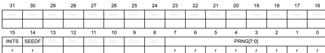
| 31 | 30 | 29 | 28 | 27 | 26 | 25 | 24 | 23 | 22 | 21 | 20 | 19 | 18 | 17 | 16 |
| Res. | Res. | Res. | Res. | Res. | Res. | Res. | Res. | Res. | Res. | Res. | Res. | Res. | Res. | Res. | Res. |
| 15 | 14 | 13 | 12 | 11 | 10 | 9 | 8 | 7 | 6 | 5 | 4 | 3 | 2 | 1 | 0 |
| INITS | SEEDF | Res. | Res. | Res. | Res. | Res. | Res. | PRNG[7:0] | |||||||
| r | r | r | r | r | r | r | r | r | r | ||||||
Bits 31:16 Reserved, must be kept at reset value.
Bit 15 INITS : Active tamper initialization status
This flag is set by hardware when the PRNG has absorbed the first 128-bit seed, meaning that the enabled active tamper are functional. This flag is cleared when the active tamper are disabled.
Bit 14 SEEDF : Seed running flag
This flag is set by hardware when a new seed is written in the TAMP_ATSEEDR. It is cleared by hardware when the PRNG has absorbed this new seed, and by system reset. The TAMP APB clock must not be switched off as long as SEEDF is set.
Bits 13:8 Reserved, must be kept at reset value.
Bits 7:0 PRNG[7:0] : Pseudo-random generator value
This field provides the values of the PRNG output. Because of potential inconsistencies due to synchronization delays, PRNG must be read at least twice. The read value is correct if it is equal to previous read value.
This field can only be read when the APB is in secure mode.
64.7.8 TAMP active tamper control register 2 (TAMP_ATCR2)
This register can be protected against nonsecure access. Refer to Section 64.4.5: TAMP secure protection modes .
This register can be protected against unprivileged access. Refer to Section 64.4.7: TAMP privilege protection modes .
Address offset: 0x1C
Backup domain reset value: 0x0000 0000
System reset: not affected
| 31 | 30 | 29 | 28 | 27 | 26 | 25 | 24 | 23 | 22 | 21 | 20 | 19 | 18 | 17 | 16 |
|---|---|---|---|---|---|---|---|---|---|---|---|---|---|---|---|
| ATOSEL8[2:0] | ATOSEL7[2:0] | ATOSEL6[2:0] | ATOSEL5[2:0] | ATOSEL4[2:0] | ATOSEL3[2] | ||||||||||
| rw | rw | rw | rw | rw | rw | rw | rw | rw | rw | rw | rw | rw | rw | rw | rw |
| 15 | 14 | 13 | 12 | 11 | 10 | 9 | 8 | 7 | 6 | 5 | 4 | 3 | 2 | 1 | 0 |
| ATOSEL3[1:0] | ATOSEL2[2:0] | ATOSEL1[2:0] | Res. | Res. | Res. | Res. | Res. | Res. | Res. | Res. | |||||
| rw | rw | rw | rw | rw | rw | rw | rw | ||||||||
Bits 31:29 ATOSEL8[2:0] : Active tamper shared output 8 selection
000: TAMPOUTSEL8 = TAMP_OUT1
001: TAMPOUTSEL8 = TAMP_OUT2
010: TAMPOUTSEL8 = TAMP_OUT3
011: TAMPOUTSEL8 = TAMP_OUT4
100: TAMPOUTSEL8 = TAMP_OUT5
101: TAMPOUTSEL8 = TAMP_OUT6
110: TAMPOUTSEL8 = TAMP_OUT7
111: TAMPOUTSEL8 = TAMP_OUT8
If the TAMP_OUTx output is not available in the package pinout, the output selection value is reserved and must not be used.
Bits 28:26 ATOSEL7[2:0] : Active tamper shared output 7 selection
000: TAMPOUTSEL7 = TAMP_OUT1
001: TAMPOUTSEL7 = TAMP_OUT2
010: TAMPOUTSEL7 = TAMP_OUT3
011: TAMPOUTSEL7 = TAMP_OUT4
100: TAMPOUTSEL7 = TAMP_OUT5
101: TAMPOUTSEL7 = TAMP_OUT6
110: TAMPOUTSEL7 = TAMP_OUT7
111: TAMPOUTSEL7 = TAMP_OUT8
If the TAMP_OUTx output is not available in the package pinout, the output selection value is reserved and must not be used.
Bits 25:23 ATOSEL6[2:0] : Active tamper shared output 6 selection
000: TAMPOUTSEL6 = TAMP_OUT1
001: TAMPOUTSEL6 = TAMP_OUT2
010: TAMPOUTSEL6 = TAMP_OUT3
011: TAMPOUTSEL6 = TAMP_OUT4
100: TAMPOUTSEL6 = TAMP_OUT5
101: TAMPOUTSEL6 = TAMP_OUT6
110: TAMPOUTSEL6 = TAMP_OUT7
111: TAMPOUTSEL6 = TAMP_OUT8
If the TAMP_OUTx output is not available in the package pinout, the output selection value is reserved and must not be used.
Bits 22:20 ATOSEL5[2:0] : Active tamper shared output 5 selection
000: TAMPOUTSEL5 = TAMP_OUT1
001: TAMPOUTSEL5 = TAMP_OUT2
010: TAMPOUTSEL5 = TAMP_OUT3
011: TAMPOUTSEL5 = TAMP_OUT4
100: TAMPOUTSEL5 = TAMP_OUT5
101: TAMPOUTSEL5 = TAMP_OUT6
110: TAMPOUTSEL5 = TAMP_OUT7
111: TAMPOUTSEL5 = TAMP_OUT8
If the TAMP_OUTx output is not available in the package pinout, the output selection value is reserved and must not be used.
Bits 19:17 ATOSEL4[2:0] : Active tamper shared output 4 selection
000: TAMPOUTSEL4 = TAMP_OUT1
001: TAMPOUTSEL4 = TAMP_OUT2
010: TAMPOUTSEL4 = TAMP_OUT3
011: TAMPOUTSEL4 = TAMP_OUT4
100: TAMPOUTSEL4 = TAMP_OUT5
101: TAMPOUTSEL4 = TAMP_OUT6
110: TAMPOUTSEL4 = TAMP_OUT7
111: TAMPOUTSEL4 = TAMP_OUT8
If the TAMP_OUTx output is not available in the package pinout, the output selection value is reserved and must not be used.
Bits 18:17 are the mirror of ATOSEL4[1:0] in the TAMP_ATCR1, and so can also be read or written through TAMP_ATCR1.
Bits 16:14 ATOSEL3[2:0] : Active tamper shared output 3 selection
000: TAMPOUTSEL3 = TAMP_OUT1
001: TAMPOUTSEL3 = TAMP_OUT2
010: TAMPOUTSEL3 = TAMP_OUT3
011: TAMPOUTSEL3 = TAMP_OUT4
100: TAMPOUTSEL3 = TAMP_OUT5
101: TAMPOUTSEL3 = TAMP_OUT6
110: TAMPOUTSEL3 = TAMP_OUT7
111: TAMPOUTSEL3 = TAMP_OUT8
If the TAMP_OUTx output is not available in the package pinout, the output selection value is reserved and must not be used.
Bits 15:14 are the mirror of ATOSEL3[1:0] in the TAMP_ATCR1, and so can also be read or written through TAMP_ATCR1.
Bits 13:11 ATOSEL2[2:0] : Active tamper shared output 2 selection
000: TAMPOUTSEL2 = TAMP_OUT1
001: TAMPOUTSEL2 = TAMP_OUT2
010: TAMPOUTSEL2 = TAMP_OUT3
011: TAMPOUTSEL2 = TAMP_OUT4
100: TAMPOUTSEL2 = TAMP_OUT5
101: TAMPOUTSEL2 = TAMP_OUT6
110: TAMPOUTSEL2 = TAMP_OUT7
111: TAMPOUTSEL2 = TAMP_OUT8
If the TAMP_OUTx output is not available in the package pinout, the output selection value is reserved and must not be used.
Bits 12:11 are the mirror of ATOSEL2[1:0] in the TAMP_ATCR1, and so can also be read or written through TAMP_ATCR1.
Bits 10:8 ATOSEL1[2:0] : Active tamper shared output 1 selection
000: TAMPOUTSEL1 = TAMP_OUT1
001: TAMPOUTSEL1 = TAMP_OUT2
010: TAMPOUTSEL1 = TAMP_OUT3
011: TAMPOUTSEL1 = TAMP_OUT4
100: TAMPOUTSEL1 = TAMP_OUT5
101: TAMPOUTSEL1 = TAMP_OUT6
110: TAMPOUTSEL1 = TAMP_OUT7
111: TAMPOUTSEL1 = TAMP_OUT8
If the TAMP_OUTx output is not available in the package pinout, the output selection value is reserved and must not be used.
Bits 9:8 are the mirror of ATOSEL1[1:0] in the TAMP_ATCR1, and so can also be read or written through TAMP_ATCR1.
Bits 7:0 Reserved, must be kept at reset value.
Note: Changing the active tamper configuration in this register is not allowed when a TAMPxAM bit is set, unless the corresponding TAMPxE bits are all cleared in the TAMP_CR1 register. All tamper configured in active mode must be enabled at the same time (by setting all related TAMPxE in the same TAMP_CR1 write). All tamper configured in active mode must be disabled at the same time (by clearing all related TAMPxE in the same TAMP_CR1 write). A minimum duration of 1 CK_ATPRE period must be waited for after disabling the active tamper and before re-enabling them.
64.7.9 TAMP secure configuration register (TAMP_SECCFGR)
If TZEN = 1, this register can be written only when the APB access is secure. If TZEN = 0, BKPRWSEC[7:0], BKPWSEC[7:0] and BHKLOCK can be written with nonsecure APB access, and TAMPSEC, CNT1SEC cannot be written.
This register can be globally write-protected, or each bit of this register can be individually write-protected against unprivileged access depending on the TAMP_PRIVCFGR configuration (refer to Section 64.4.7: TAMP privilege protection modes ).
Address offset: 0x20
Backup domain reset value: 0x0000 0000
System reset: not affected
| 31 | 30 | 29 | 28 | 27 | 26 | 25 | 24 | 23 | 22 | 21 | 20 | 19 | 18 | 17 | 16 |
|---|---|---|---|---|---|---|---|---|---|---|---|---|---|---|---|
| TAMP SEC | BHK LOCK | Res. | Res. | Res. | Res. | Res. | Res. | BKPWSEC[7:0] | |||||||
| rw | rs | rw | rw | rw | rw | rw | rw | rw | rw | ||||||
| 15 | 14 | 13 | 12 | 11 | 10 | 9 | 8 | 7 | 6 | 5 | 4 | 3 | 2 | 1 | 0 |
| CNT1 SEC | Res. | Res. | Res. | Res. | Res. | Res. | Res. | BKPRWSEC[7:0] | |||||||
| rw | rw | rw | rw | rw | rw | rw | rw | rw | |||||||
Bit 31 TAMPSEC : Tamper protection (excluding monotonic counters and backup registers)
0: Tamper configuration and interrupt can be written when the APB access is secure or nonsecure.
1: Tamper configuration and interrupt can be written only when the APB access is secure.
Note: Refer to Section 64.4.5: TAMP secure protection modes for details on the read protection.
Bit 30 BHKLOCK : Boot hardware key lock
This bit can be read and can only be written to 1 by software. It is cleared by hardware together with the backup registers following a tamper detection event or when the readout protection (RDP) is disabled.
0: The Backup registers from TAMP_BKP0R to TAMP_BKP7R can be accessed according to the Protection zone they belong to.
1: The backup registers from TAMP_BKP0R to TAMP_BKP7R cannot be accessed neither in read nor in write (they are read as 0 and write ignore).
Bits 29:24 Reserved, must be kept at reset value.
Bits 23:16 BKPWSEC[7:0] : Backup registers write protection offset
BKPWSEC value must be from 0 to 32.
Protection zone 2 is defined for backup registers from TAMP_BKPyR (y = BKPRWSEC) to TAMP_BKPzR (z = BKPWSEC-1, with BKPWSEC > BKPRWSEC):
- - if TZEN=1, these backup registers can be written only with secure access.
- - They can be read with secure or nonsecure access.
If BKPWSEC = 0 or if BKPWSEC ≤ BKPRWSEC: there is no protection zone 2.
Protection zone 3 is defined for backup registers from TAMP_BKPtR (t = BKPWSEC if BKPWSEC ≥ BKPRWSEC, else t = BKPRWSEC).
- - They can be read or written with secure or nonsecure access.
If BKPWSEC = 32: there is no protection zone 3.
Refer to Figure 775: Backup registers protection zones.
Note: If TZEN=0: the protection zone 2 can be read and written with nonsecure access.
Note: If BKPWPRIV is set, BKPWSEC[7:0] can be written only in privileged mode.
Bit 15 CNT1SEC : Monotonic counter 1 secure protection
0: Monotonic counter 1 (TAMP_COUNT1R) can be read and written when the APB access is secure or nonsecure.
1: Monotonic counter 1 (TAMP_COUNT1R) can be read and written only when the APB access is secure.
Bits 14:8 Reserved, must be kept at reset value.
Bits 7:0 BKPRWSEC[7:0] : Backup registers read/write protection offset
BKPRWSEC value must be from 0 to 32.
Protection zone 1 is defined for backup registers from TAMP_BKP0R to TAMP_BKPxR ( \( x = \text{BKPRWSEC}-1 \) , with \( \text{BKPRWSEC} \geq 1 \) ).
– if TZEN=1, these backup registers can be read and written only with secure access.
If BKPRWSEC = 0: there is no protection zone 1.
Refer to Figure 775: Backup registers protection zones .
Note: If TZEN=0: the protection zone 1 can be read and written with nonsecure access.
Note: If BKPRWPRIV or BKPWPRIV is set, BKPRWSEC[7:0] can be written only in privileged mode.
64.7.10 TAMP privilege configuration register (TAMP_PRIVCFGR)
This register can be written only when the APB access is privileged.
When TZEN = 1, this register can be write-protected, or each bit of this register can be individually write-protected against nonsecure access depending on the TAMP_SECCFGR configuration (refer to Section 64.4.5: TAMP secure protection modes ). BKPWPRIV and BKPRWPRIV can be written in secure mode only.
Address offset: 0x24
Backup domain reset value: 0x0000 0000
System reset: not affected
| 31 | 30 | 29 | 28 | 27 | 26 | 25 | 24 | 23 | 22 | 21 | 20 | 19 | 18 | 17 | 16 |
|---|---|---|---|---|---|---|---|---|---|---|---|---|---|---|---|
| TAMP PRIV | BKP WPRIV | BKPR WPRIV | Res. | Res. | Res. | Res. | Res. | Res. | Res. | Res. | Res. | Res. | Res. | Res. | Res. |
| rw | rw | rw | |||||||||||||
| 15 | 14 | 13 | 12 | 11 | 10 | 9 | 8 | 7 | 6 | 5 | 4 | 3 | 2 | 1 | 0 |
| CNT1 PRIV | Res. | Res. | Res. | Res. | Res. | Res. | Res. | Res. | Res. | Res. | Res. | Res. | Res. | Res. | Res. |
| rw |
Bit 31 TAMPPRIV : Tamper privilege protection (excluding monotonic counters and backup registers)
0: Tamper configuration and interrupt can be written with privileged or unprivileged access.
1: Tamper configuration and interrupt can be written only with privileged access.
Note: Refer to Section 64.4.7: TAMP privilege protection modes for details on the read protection.
Bit 30 BKPWPRIV : Backup registers zone 2 privilege protection
0: Backup registers zone 2 can be written with privileged or unprivileged access.
1: Backup registers zone 2 can be written only with privileged access.
Bit 29 BKPRWPRIV : Backup registers zone 1 privilege protection
0: Backup registers zone 1 can be read and written with privileged or unprivileged access.
1: Backup registers zone 1 can be read and written only with privileged access
Bits 28:16 Reserved, must be kept at reset value.
Bit 15 CNT1PRIV : Monotonic counter 1 privilege protection
0: Monotonic counter 1 (TAMP_COUNT1R) can be read and written when the APB access is privileged or unprivileged.
1: Monotonic counter 1 (TAMP_COUNT1R) can be read and written only when the APB access is privileged.
Bits 14:0 Reserved, must be kept at reset value.
64.7.11 TAMP interrupt enable register (TAMP_IER)
This register can be protected against nonsecure access. Refer to Section 64.4.5: TAMP secure protection modes .
This register can be protected against unprivileged access. Refer to Section 64.4.7: TAMP privilege protection modes .
Address offset: 0x2C
Backup domain reset value: 0x0000 0000
System reset: not affected
| 31 | 30 | 29 | 28 | 27 | 26 | 25 | 24 | 23 | 22 | 21 | 20 | 19 | 18 | 17 | 16 |
|---|---|---|---|---|---|---|---|---|---|---|---|---|---|---|---|
| Res. | Res. | Res. | ITAMP13IE | ITAMP12IE | ITAMP11IE | Res. | ITAMP9IE | ITAMP8IE | ITAMP7IE | ITAMP6IE | ITAMP5IE | Res. | ITAMP3IE | ITAMP2IE | ITAMP1IE |
| rw | rw | rw | rw | rw | rw | rw | rw | rw | rw | rw |
| 15 | 14 | 13 | 12 | 11 | 10 | 9 | 8 | 7 | 6 | 5 | 4 | 3 | 2 | 1 | 0 |
|---|---|---|---|---|---|---|---|---|---|---|---|---|---|---|---|
| Res. | Res. | Res. | Res. | Res. | Res. | Res. | Res. | TAMP8IE | TAMP7IE | TAMP6IE | TAMP5IE | TAMP4IE | TAMP3IE | TAMP2IE | TAMP1IE |
| rw | rw | rw | rw | rw | rw | rw | rw |
Bit 31 Reserved, must be kept at reset value.
Bit 30 Reserved, must be kept at reset value.
Bit 29 Reserved, must be kept at reset value.
Bit 28 ITAMP13IE : Internal tamper 13 interrupt enable
0: Internal tamper 13 interrupt disabled.
1: Internal tamper 13 interrupt enabled.
- Bit 27
ITAMP12IE
: Internal tamper 12 interrupt enable
0: Internal tamper 12 interrupt disabled.
1: Internal tamper 12 interrupt enabled. - Bit 26
ITAMP11IE
: Internal tamper 11 interrupt enable
0: Internal tamper 11 interrupt disabled.
1: Internal tamper 11 interrupt enabled. - Bit 25 Reserved, must be kept at reset value.
- Bit 24
ITAMP9IE
: Internal tamper 9 interrupt enable
0: Internal tamper 9 interrupt disabled.
1: Internal tamper 9 interrupt enabled. - Bit 23
ITAMP8IE
: Internal tamper 8 interrupt enable
0: Internal tamper 8 interrupt disabled.
1: Internal tamper 8 interrupt enabled. - Bit 22
ITAMP7IE
: Internal tamper 7 interrupt enable
0: Internal tamper 7 interrupt disabled.
1: Internal tamper 7 interrupt enabled. - Bit 21
ITAMP6IE
: Internal tamper 6 interrupt enable
0: Internal tamper 6 interrupt disabled.
1: Internal tamper 6 interrupt enabled. - Bit 20
ITAMP5IE
: Internal tamper 5 interrupt enable
0: Internal tamper 5 interrupt disabled.
1: Internal tamper 5 interrupt enabled. - Bit 19 Reserved, must be kept at reset value.
- Bit 18
ITAMP3IE
: Internal tamper 3 interrupt enable
0: Internal tamper 3 interrupt disabled.
1: Internal tamper 3 interrupt enabled. - Bit 17
ITAMP2IE
: Internal tamper 2 interrupt enable
0: Internal tamper 2 interrupt disabled.
1: Internal tamper 2 interrupt enabled. - Bit 16
ITAMP1IE
: Internal tamper 1 interrupt enable
0: Internal tamper 1 interrupt disabled.
1: Internal tamper 1 interrupt enabled - Bits 15:8 Reserved, must be kept at reset value.
- Bit 7
TAMP8IE
: Tamper 8 interrupt enable
0: Tamper 8 interrupt disabled.
1: Tamper 8 interrupt enabled. - Bit 6
TAMP7IE
: Tamper 7 interrupt enable
0: Tamper 7 interrupt disabled.
1: Tamper 7 interrupt enabled. - Bit 5
TAMP6IE
: Tamper 6 interrupt enable
0: Tamper 6 interrupt disabled.
1: Tamper 6 interrupt enabled.
- Bit 4
TAMP5IE
: Tamper 5 interrupt enable
- 0: Tamper 5 interrupt disabled.
- 1: Tamper 5 interrupt enabled.
- Bit 3
TAMP4IE
: Tamper 4 interrupt enable
- 0: Tamper 4 interrupt disabled.
- 1: Tamper 4 interrupt enabled.
- Bit 2
TAMP3IE
: Tamper 3 interrupt enable
- 0: Tamper 3 interrupt disabled.
- 1: Tamper 3 interrupt enabled..
- Bit 1
TAMP2IE
: Tamper 2 interrupt enable
- 0: Tamper 2 interrupt disabled.
- 1: Tamper 2 interrupt enabled.
- Bit 0
TAMP1IE
: Tamper 1 interrupt enable
- 0: Tamper 1 interrupt disabled.
- 1: Tamper 1 interrupt enabled.
64.7.12 TAMP status register (TAMP_SR)
This register can be protected against nonsecure access. Refer to Section 64.4.5: TAMP secure protection modes .
This register can be protected against unprivileged access. Refer to Section 64.4.7: TAMP privilege protection modes .
Address offset: 0x30
Backup domain reset value: 0x0000 0000
System reset: not affected
| 31 | 30 | 29 | 28 | 27 | 26 | 25 | 24 | 23 | 22 | 21 | 20 | 19 | 18 | 17 | 16 |
|---|---|---|---|---|---|---|---|---|---|---|---|---|---|---|---|
| Res. | Res. | Res. | ITAMP13F | ITAMP12F | ITAMP11F | Res. | ITAMP9F | ITAMP8F | ITAMP7F | ITAMP6F | ITAMP5F | Res. | ITAMP3F | ITAMP2F | ITAMP1F |
| r | r | r | r | r | r | r | r | r | r | r | |||||
| 15 | 14 | 13 | 12 | 11 | 10 | 9 | 8 | 7 | 6 | 5 | 4 | 3 | 2 | 1 | 0 |
| Res. | Res. | Res. | Res. | Res. | Res. | Res. | Res. | TAMP8F | TAMP7F | TAMP6F | TAMP5F | TAMP4F | TAMP3F | TAMP2F | TAMP1F |
| r | r | r | r | r | r | r | r |
- Bit 31 Reserved, must be kept at reset value.
- Bit 30 Reserved, must be kept at reset value.
- Bit 29 Reserved, must be kept at reset value.
- Bit 28
ITAMP13F
: Internal tamper 13 flag
- This flag is set by hardware when a tamper detection event is detected on the internal tamper 13.
- Bit 27
ITAMP12F
: Internal tamper 12 flag
- This flag is set by hardware when a tamper detection event is detected on the internal tamper 12.
- Bit 26
ITAMP11F
: Internal tamper 11 flag
This flag is set by hardware when a tamper detection event is detected on the internal tamper 11. - Bit 25 Reserved, must be kept at reset value.
- Bit 24
ITAMP9F
: Internal tamper 9 flag
This flag is set by hardware when a tamper detection event is detected on the internal tamper 9. - Bit 23
ITAMP8F
: Internal tamper 8 flag
This flag is set by hardware when a tamper detection event is detected on the internal tamper 8. - Bit 22
ITAMP7F
: Internal tamper 7 flag
This flag is set by hardware when a tamper detection event is detected on the internal tamper 7. - Bit 21
ITAMP6F
: Internal tamper 6 flag
This flag is set by hardware when a tamper detection event is detected on the internal tamper 6. - Bit 20
ITAMP5F
: Internal tamper 5 flag
This flag is set by hardware when a tamper detection event is detected on the internal tamper 5. - Bit 19 Reserved, must be kept at reset value.
- Bit 18
ITAMP3F
: Internal tamper 3 flag
This flag is set by hardware when a tamper detection event is detected on the internal tamper 3. - Bit 17
ITAMP2F
: Internal tamper 2 flag
This flag is set by hardware when a tamper detection event is detected on the internal tamper 2. - Bit 16
ITAMP1F
: Internal tamper 1 flag
This flag is set by hardware when a tamper detection event is detected on the internal tamper 1. - Bits 15:8 Reserved, must be kept at reset value.
- Bit 7
TAMP8F
: TAMP8 detection flag
This flag is set by hardware when a tamper detection event is detected on the TAMP8 input. - Bit 6
TAMP7F
: TAMP7 detection flag
This flag is set by hardware when a tamper detection event is detected on the TAMP7 input. - Bit 5
TAMP6F
: TAMP6 detection flag
This flag is set by hardware when a tamper detection event is detected on the TAMP6 input. - Bit 4
TAMP5F
: TAMP5 detection flag
This flag is set by hardware when a tamper detection event is detected on the TAMP5 input. - Bit 3
TAMP4F
: TAMP4 detection flag
This flag is set by hardware when a tamper detection event is detected on the TAMP4 input.
Bit 2 TAMP3F : TAMP3 detection flag
This flag is set by hardware when a tamper detection event is detected on the TAMP3 input.
Bit 1 TAMP2F : TAMP2 detection flag
This flag is set by hardware when a tamper detection event is detected on the TAMP2 input.
Bit 0 TAMP1F : TAMP1 detection flag
This flag is set by hardware when a tamper detection event is detected on the TAMP1 input.
64.7.13 TAMP nonsecure masked interrupt status register (TAMP_MISR)
This register can be protected against unprivileged access. Refer to Section 64.4.7: TAMP privilege protection modes .
Address offset: 0x34
Backup domain reset value: 0x0000 0000
System reset: not affected
| 31 | 30 | 29 | 28 | 27 | 26 | 25 | 24 | 23 | 22 | 21 | 20 | 19 | 18 | 17 | 16 |
|---|---|---|---|---|---|---|---|---|---|---|---|---|---|---|---|
| Res. | Res. | Res. | ITAMP13MF | ITAMP12MF | ITAMP11MF | Res. | ITAMP9MF | ITAMP8MF | ITAMP7MF | ITAMP6MF | ITAMP5MF | Res. | ITAMP3MF | ITAMP2MF | ITAMP1MF |
| r | r | r | r | r | r | r | r | r | r | r | |||||
| 15 | 14 | 13 | 12 | 11 | 10 | 9 | 8 | 7 | 6 | 5 | 4 | 3 | 2 | 1 | 0 |
| Res. | Res. | Res. | Res. | Res. | Res. | Res. | Res. | TAMP8MF | TAMP7MF | TAMP6MF | TAMP5MF | TAMP4MF | TAMP3MF | TAMP2MF | TAMP1MF |
| r | r | r | r | r | r | r | r |
Bit 31 Reserved, must be kept at reset value.
Bit 30 Reserved, must be kept at reset value.
Bit 29 Reserved, must be kept at reset value.
Bit 28 ITAMP13MF : internal tamper 13 nonsecure interrupt masked flag
This flag is set by hardware when the internal tamper 13 nonsecure interrupt is raised.
Bit 27 ITAMP12MF : internal tamper 12 nonsecure interrupt masked flag
This flag is set by hardware when the internal tamper 12 nonsecure interrupt is raised.
Bit 26 ITAMP11MF : internal tamper 11 nonsecure interrupt masked flag
This flag is set by hardware when the internal tamper 11 nonsecure interrupt is raised.
Bit 25 Reserved, must be kept at reset value.
Bit 24 ITAMP9MF : internal tamper 9 nonsecure interrupt masked flag
This flag is set by hardware when the internal tamper 9 nonsecure interrupt is raised.
Bit 23 ITAMP8MF : Internal tamper 8 nonsecure interrupt masked flag
This flag is set by hardware when the internal tamper 8 nonsecure interrupt is raised.
Bit 22 ITAMP7MF : Internal tamper 7 tamper nonsecure interrupt masked flag
This flag is set by hardware when the internal tamper 7 nonsecure interrupt is raised.
Bit 21 ITAMP6MF : Internal tamper 6 nonsecure interrupt masked flag
This flag is set by hardware when the internal tamper 6 nonsecure interrupt is raised.
Bit 20 ITAMP5MF : Internal tamper 5 nonsecure interrupt masked flag
This flag is set by hardware when the internal tamper 5 nonsecure interrupt is raised.
Bit 19 Reserved, must be kept at reset value.
Bit 18 ITAMP3MF : Internal tamper 3 nonsecure interrupt masked flag
This flag is set by hardware when the internal tamper 3 nonsecure interrupt is raised.
Bit 17 ITAMP2MF : Internal tamper 2 nonsecure interrupt masked flag
This flag is set by hardware when the internal tamper 2 nonsecure interrupt is raised.
Bit 16 ITAMP1MF : Internal tamper 1 nonsecure interrupt masked flag
This flag is set by hardware when the internal tamper 1 nonsecure interrupt is raised.
Bits 15:8 Reserved, must be kept at reset value.
Bit 7 TAMP8MF : TAMP8 nonsecure interrupt masked flag
This flag is set by hardware when the tamper 8 nonsecure interrupt is raised.
Bit 6 TAMP7MF : TAMP7 nonsecure interrupt masked flag
This flag is set by hardware when the tamper 7 nonsecure interrupt is raised.
Bit 5 TAMP6MF : TAMP6 nonsecure interrupt masked flag
This flag is set by hardware when the tamper 6 nonsecure interrupt is raised.
Bit 4 TAMP5MF : TAMP5 nonsecure interrupt masked flag
This flag is set by hardware when the tamper 5 nonsecure interrupt is raised.
Bit 3 TAMP4MF : TAMP4 nonsecure interrupt masked flag
This flag is set by hardware when the tamper 4 nonsecure interrupt is raised.
Bit 2 TAMP3MF : TAMP3 nonsecure interrupt masked flag
This flag is set by hardware when the tamper 3 nonsecure interrupt is raised.
Bit 1 TAMP2MF : TAMP2 nonsecure interrupt masked flag
This flag is set by hardware when the tamper 2 nonsecure interrupt is raised.
Bit 0 TAMP1MF : TAMP1 nonsecure interrupt masked flag
This flag is set by hardware when the tamper 1 nonsecure interrupt is raised.
64.7.14 TAMP secure masked interrupt status register (TAMP_SMISR)
This register can be protected against nonsecure access. Refer to Section 64.4.5: TAMP secure protection modes .
This register can be protected against unprivileged access. Refer to Section 64.4.7: TAMP privilege protection modes .
Address offset: 0x38
Backup domain reset value: 0x0000 0000
System reset: not affected
| 31 | 30 | 29 | 28 | 27 | 26 | 25 | 24 | 23 | 22 | 21 | 20 | 19 | 18 | 17 | 16 |
|---|---|---|---|---|---|---|---|---|---|---|---|---|---|---|---|
| Res. | Res. | Res. | ITAMP1 3MF | ITAMP1 2MF | ITAMP1 1MF | Res. | ITAMP9 MF | ITAMP8 MF | ITAMP 7MF | ITAMP6 MF | ITAMP5 MF | Res. | ITAMP3 MF | ITAMP2 MF | ITAMP1 MF |
| r | r | r | r | r | r | r | r | r | r | r | |||||
| 15 | 14 | 13 | 12 | 11 | 10 | 9 | 8 | 7 | 6 | 5 | 4 | 3 | 2 | 1 | 0 |
| Res. | Res. | Res. | Res. | Res. | Res. | Res. | Res. | TAMP 8MF | TAMP 7MF | TAMP 6MF | TAMP 5MF | TAMP 4MF | TAMP 3MF | TAMP 2MF | TAMP 1MF |
| r | r | r | r | r | r | r | r |
- Bit 31 Reserved, must be kept at reset value.
- Bit 30 Reserved, must be kept at reset value.
- Bit 29 Reserved, must be kept at reset value.
- Bit 28
ITAMP13MF
: internal tamper 13 secure interrupt masked flag
This flag is set by hardware when the internal tamper 13 secure interrupt is raised. - Bit 27
ITAMP12MF
: internal tamper 12 secure interrupt masked flag
This flag is set by hardware when the internal tamper 12 secure interrupt is raised. - Bit 26
ITAMP11MF
: internal tamper 11 secure interrupt masked flag
This flag is set by hardware when the internal tamper 11 secure interrupt is raised. - Bit 25 Reserved, must be kept at reset value.
- Bit 24
ITAMP9MF
: internal tamper 9 secure interrupt masked flag
This flag is set by hardware when the internal tamper 9 secure interrupt is raised. - Bit 23
ITAMP8MF
: Internal tamper 8 secure interrupt masked flag
This flag is set by hardware when the internal tamper 8 secure interrupt is raised. - Bit 22
ITAMP7MF
: Internal tamper 7 secure interrupt masked flag
This flag is set by hardware when the internal tamper 7 secure interrupt is raised. - Bit 21
ITAMP6MF
: Internal tamper 6 secure interrupt masked flag
This flag is set by hardware when the internal tamper 6 secure interrupt is raised. - Bit 20
ITAMP5MF
: Internal tamper 5 secure interrupt masked flag
This flag is set by hardware when the internal tamper 5 secure interrupt is raised. - Bit 19 Reserved, must be kept at reset value.
- Bit 18
ITAMP3MF
: Internal tamper 3 secure interrupt masked flag
This flag is set by hardware when the internal tamper 3 secure interrupt is raised. - Bit 17
ITAMP2MF
: Internal tamper 2 secure interrupt masked flag
This flag is set by hardware when the internal tamper 2 secure interrupt is raised. - Bit 16
ITAMP1MF
: Internal tamper 1 secure interrupt masked flag
This flag is set by hardware when the internal tamper 1 secure interrupt is raised. - Bits 15:8 Reserved, must be kept at reset value.
- Bit 7
TAMP8MF
: TAMP8 secure interrupt masked flag
This flag is set by hardware when the tamper 8 secure interrupt is raised. - Bit 6
TAMP7MF
: TAMP7 secure interrupt masked flag
This flag is set by hardware when the tamper 7 secure interrupt is raised. - Bit 5
TAMP6MF
: TAMP6 secure interrupt masked flag
This flag is set by hardware when the tamper 6 secure interrupt is raised. - Bit 4
TAMP5MF
: TAMP5 secure interrupt masked flag
This flag is set by hardware when the tamper 5 secure interrupt is raised. - Bit 3
TAMP4MF
: TAMP4 secure interrupt masked flag
This flag is set by hardware when the tamper 4 secure interrupt is raised.
Bit 2 TAMP3MF : TAMP3 secure interrupt masked flag
This flag is set by hardware when the tamper 3 secure interrupt is raised.
Bit 1 TAMP2MF : TAMP2 secure interrupt masked flag
This flag is set by hardware when the tamper 2 secure interrupt is raised.
Bit 0 TAMP1MF : TAMP1 secure interrupt masked flag
This flag is set by hardware when the tamper 1 secure interrupt is raised.
64.7.15 TAMP status clear register (TAMP_SCR)
This register can be protected against nonsecure access. Refer to Section 64.4.5: TAMP secure protection modes .
This register can be protected against unprivileged access. Refer to Section 64.4.7: TAMP privilege protection modes .
Address offset: 0x3C
System reset value: 0x0000 0000
| 31 | 30 | 29 | 28 | 27 | 26 | 25 | 24 | 23 | 22 | 21 | 20 | 19 | 18 | 17 | 16 |
|---|---|---|---|---|---|---|---|---|---|---|---|---|---|---|---|
| Res. | Res. | Res. | C ITAMP 13F | C ITAMP 12F | C ITAMP 11F | Res. | C ITAMP 9F | C ITAMP 8F | C ITAMP 7F | C ITAMP 6F | C ITAMP 5F | Res. | C ITAMP 3F | C ITAMP 2F | C ITAMP 1F |
| w | w | w | w | w | w | w | w | w | w | w | |||||
| 15 | 14 | 13 | 12 | 11 | 10 | 9 | 8 | 7 | 6 | 5 | 4 | 3 | 2 | 1 | 0 |
| Res. | Res. | Res. | Res. | Res. | Res. | Res. | Res. | CTAMP 8F | CTAMP 7F | CTAMP 6F | CTAMP 5F | CTAMP 4F | CTAMP 3F | CTAMP 2F | CTAMP 1F |
| w | w | w | w | w | w | w | w |
Bit 31 Reserved, must be kept at reset value.
Bit 30 Reserved, must be kept at reset value.
Bit 29 Reserved, must be kept at reset value.
Bit 28 CITAMP13F : Clear ITAMP13 detection flag
Writing 1 in this bit clears the ITAMP13F bit in the TAMP_SR register.
Bit 27 CITAMP12F : Clear ITAMP12 detection flag
Writing 1 in this bit clears the ITAMP12F bit in the TAMP_SR register.
Bit 26 CITAMP11F : Clear ITAMP11 detection flag
Writing 1 in this bit clears the ITAMP11F bit in the TAMP_SR register.
Bit 25 Reserved, must be kept at reset value.
Bit 24 CITAMP9F : Clear ITAMP9 detection flag
Writing 1 in this bit clears the ITAMP9F bit in the TAMP_SR register.
Bit 23 CITAMP8F : Clear ITAMP8 detection flag
Writing 1 in this bit clears the ITAMP8F bit in the TAMP_SR register.
Bit 22 CITAMP7F : Clear ITAMP7 detection flag
Writing 1 in this bit clears the ITAMP7F bit in the TAMP_SR register.
Bit 21 CITAMP6F : Clear ITAMP6 detection flag
Writing 1 in this bit clears the ITAMP6F bit in the TAMP_SR register.
- Bit 20
CITAMP5F
: Clear ITAMP5 detection flag
Writing 1 in this bit clears the ITAMP5F bit in the TAMP_SR register. - Bit 19 Reserved, must be kept at reset value.
- Bit 18
CITAMP3F
: Clear ITAMP3 detection flag
Writing 1 in this bit clears the ITAMP3F bit in the TAMP_SR register. - Bit 17
CITAMP2F
: Clear ITAMP2 detection flag
Writing 1 in this bit clears the ITAMP2F bit in the TAMP_SR register. - Bit 16
CITAMP1F
: Clear ITAMP1 detection flag
Writing 1 in this bit clears the ITAMP1F bit in the TAMP_SR register. - Bits 15:8 Reserved, must be kept at reset value.
- Bit 7
CTAMP8F
: Clear TAMP8 detection flag
Writing 1 in this bit clears the TAMP8F bit in the TAMP_SR register. - Bit 6
CTAMP7F
: Clear TAMP7 detection flag
Writing 1 in this bit clears the TAMP7F bit in the TAMP_SR register. - Bit 5
CTAMP6F
: Clear TAMP6 detection flag
Writing 1 in this bit clears the TAMP6F bit in the TAMP_SR register. - Bit 4
CTAMP5F
: Clear TAMP5 detection flag
Writing 1 in this bit clears the TAMP5F bit in the TAMP_SR register. - Bit 3
CTAMP4F
: Clear TAMP4 detection flag
Writing 1 in this bit clears the TAMP4F bit in the TAMP_SR register. - Bit 2
CTAMP3F
: Clear TAMP3 detection flag
Writing 1 in this bit clears the TAMP3F bit in the TAMP_SR register. - Bit 1
CTAMP2F
: Clear TAMP2 detection flag
Writing 1 in this bit clears the TAMP2F bit in the TAMP_SR register. - Bit 0
CTAMP1F
: Clear TAMP1 detection flag
Writing 1 in this bit clears the TAMP1F bit in the TAMP_SR register.
64.7.16 TAMP monotonic counter 1 register (TAMP_COUNT1R)
This register can be protected against nonsecure access. Refer to Section 64.4.5: TAMP secure protection modes .
This register can be protected against unprivileged access. Refer to Section 64.4.7: TAMP privilege protection modes .
Address offset: 0x040
Backup domain reset value: 0x0000 0000
System reset: not affected
| 31 | 30 | 29 | 28 | 27 | 26 | 25 | 24 | 23 | 22 | 21 | 20 | 19 | 18 | 17 | 16 |
| COUNT[31:16] | |||||||||||||||
| rw | rw | rw | rw | rw | rw | rw | rw | rw | rw | rw | rw | rw | rw | rw | rw |
| 15 | 14 | 13 | 12 | 11 | 10 | 9 | 8 | 7 | 6 | 5 | 4 | 3 | 2 | 1 | 0 |
| COUNT[15:0] | |||||||||||||||
| rw | rw | rw | rw | rw | rw | rw | rw | rw | rw | rw | rw | rw | rw | rw | rw |
Bits 31:0 COUNT[31:0] : Monotonic counter
The monotonic counter increments by one when a write access to this register occurs, regardless of the written value. Reading this register returns the monotonic counter value. This register does not roll-over and freezes upon reaching its maximum value.
64.7.17 TAMP erase configuration register (TAMP_ERCFGR)
This register can be protected against nonsecure access. Refer to Section 64.4.5: TAMP secure protection modes .
This register can be protected against unprivileged access. Refer to Section 64.4.7: TAMP privilege protection modes .
Address offset: 0x54
Backup domain reset value: 0x0000 0000
System reset: not affected
| 31 | 30 | 29 | 28 | 27 | 26 | 25 | 24 | 23 | 22 | 21 | 20 | 19 | 18 | 17 | 16 |
| Res. | Res. | Res. | Res. | Res. | Res. | Res. | Res. | Res. | Res. | Res. | Res. | Res. | Res. | Res. | Res. |
| 15 | 14 | 13 | 12 | 11 | 10 | 9 | 8 | 7 | 6 | 5 | 4 | 3 | 2 | 1 | 0 |
| Res. | Res. | Res. | Res. | Res. | Res. | Res. | Res. | Res. | Res. | Res. | Res. | Res. | Res. | Res. | ER CFG0 |
| rw |
Bit 31 Reserved, must be kept at reset value.
Bits 30:8 Reserved, must be kept at reset value.
Bit 7 Reserved, must be kept at reset value.
Bit 6 Reserved, must be kept at reset value.
Bit 5 Reserved, must be kept at reset value.
Bit 4 Reserved, must be kept at reset value.
Bit 3 Reserved, must be kept at reset value.
Bit 2 Reserved, must be kept at reset value.
Bit 1 Reserved, must be kept at reset value.
Bit 0 ERCFG0 : Configurable resource 0 protection (1)
0: Resource 0 is not included in the device secrets protected by TAMP peripheral
1: Resource 0 is included in the device secrets protected by TAMP peripheral
- 1. Refer to tamp_confirmed_ercfg0 and tamp_potential_ercfg0 signals in Table 642: TAMP input/output pins and Table 644: TAMP interconnection .
64.7.18 TAMP backup x register (TAMP_BKPxR)
This register can be protected against nonsecure access. Refer to Section 64.4.5: TAMP secure protection modes .
This register can be protected against unprivileged access. Refer to Section 64.4.7: TAMP privilege protection modes .
Address offset: 0x100 + 0x04 * x, (x = 0 to 31)
Backup domain reset value: 0x0000 0000
System reset: not affected
| 31 | 30 | 29 | 28 | 27 | 26 | 25 | 24 | 23 | 22 | 21 | 20 | 19 | 18 | 17 | 16 |
| BKP[31:16] | |||||||||||||||
| rw | rw | rw | rw | rw | rw | rw | rw | rw | rw | rw | rw | rw | rw | rw | rw |
| 15 | 14 | 13 | 12 | 11 | 10 | 9 | 8 | 7 | 6 | 5 | 4 | 3 | 2 | 1 | 0 |
| BKP[15:0] | |||||||||||||||
| rw | rw | rw | rw | rw | rw | rw | rw | rw | rw | rw | rw | rw | w | rw | rw |
Bits 31:0 BKP[31:0]:
The application can write or read data to and from these registers.
In the default (ERASE) configuration this register is reset on a tamper detection event. It is forced to reset value as long as there is at least one internal or external tamper flag being set. This register is also reset when the readout protection (RDP) is disabled.
64.7.19 TAMP register map
Table 652. TAMP register map and reset values
| Offset | Register name | 31 | 30 | 29 | 28 | 27 | 26 | 25 | 24 | 23 | 22 | 21 | 20 | 19 | 18 | 17 | 16 | 15 | 14 | 13 | 12 | 11 | 10 | 9 | 8 | 7 | 6 | 5 | 4 | 3 | 2 | 1 | 0 | |
|---|---|---|---|---|---|---|---|---|---|---|---|---|---|---|---|---|---|---|---|---|---|---|---|---|---|---|---|---|---|---|---|---|---|---|
| 0x00 | TAMP_CR1 | Res. | Res. | Res. | ITAMP13E | ITAMP12E | ITAMP11E | Res. | ITAMP9E | ITAMP8E | ITAMP7E | ITAMP6E | ITAMP5E | Res. | ITAMP3E | ITAMP2E | ITAMP1E | Res. | Res. | Res. | Res. | Res. | Res. | Res. | Res. | TAMP8E | TAMP7E | TAMP6E | TAMP5E | TAMP4E | TAMP3E | TAMP2E | TAMP1E | |
| Reset value | 0 | 0 | 0 | 0 | 0 | 0 | 0 | 0 | 0 | 0 | 0 | 0 | 0 | 0 | 0 | 0 | 0 | 0 | 0 | |||||||||||||||
| 0x04 | TAMP_CR2 | TAMP8TRG | TAMP7TRG | TAMP6TRG | TAMP5TRG | TAMP4TRG | TAMP3TRG | TAMP2TRG | TAMP1TRG | BKERASE | BKBLOCK | Res. | Res. | Res. | TAMP3MSK | TAMP2MSK | TAMP1MSK | Res. | Res. | Res. | Res. | Res. | Res. | Res. | Res. | TAMP8NOER | TAMP7NOER | TAMP6NOER | TAMP5NOER | TAMP4NOER | TAMP3NOER | TAMP2NOER | TAMP1NOER | |
| Reset value | 0 | 0 | 0 | 0 | 0 | 0 | 0 | 0 | 0 | 0 | 0 | 0 | 0 | 0 | 0 | 0 | 0 | 0 | 0 | 0 | 0 | |||||||||||||
| 0x08 | TAMP_CR3 | Res. | Res. | Res. | Res. | Res. | Res. | Res. | Res. | Res. | Res. | Res. | Res. | Res. | Res. | Res. | Res. | Res. | Res. | Res. | ITAMP13NOER | ITAMP12NOER | ITAMP11NOER | Res. | ITAMP9NOER | ITAMP8NOER | ITAMP7NOER | ITAMP6NOER | ITAMP5NOER | Res. | ITAMP3NOER | ITAMP2NOER | ITAMP1NOER | |
| Reset value | 0 | 0 | 0 | 0 | 0 | 0 | 0 | 0 | 0 | 0 | 0 | |||||||||||||||||||||||
| 0x0C | TAMP_FLTCR | Res. | TAMPPUDIS | TAMPPRCH[1:0] | Res. | TAMPFLT[1:0] | TAMPFREQ[2:0] | |||||||||||||||||||||||||||
| Reset value | 0 | 0 | 0 | 0 | 0 | 0 | 0 | 0 | ||||||||||||||||||||||||||
| 0x10 | TAMP_ATCR1 | FLTEN | ATOSHARE | Res. | ATPER[2:0] | Res. | ATCKSEL[3:0] | ATOSEL4[1:0] | ATOSEL3[1:0] | ATOSEL2[1:0] | ATOSEL1[1:0] | TAMP8AM | TAMP7AM | TAMP6AM | TAMP5AM | TAMP4AM | TAMP3AM | TAMP2AM | TAMP1AM | |||||||||||||||
| Reset value | 0 | 0 | 0 | 0 | 0 | 0 | 1 | 1 | 1 | 0 | 0 | 0 | 0 | 0 | 0 | 0 | 0 | 0 | 0 | 0 | 0 | 0 | 0 | 0 | 0 | |||||||||
| 0x14 | TAMP_ATSEEDR | SEED[31:0] | ||||||||||||||||||||||||||||||||
| Reset value | 0 | 0 | 0 | 0 | 0 | 0 | 0 | 0 | 0 | 0 | 0 | 0 | 0 | 0 | 0 | 0 | 0 | 0 | 0 | 0 | 0 | 0 | 0 | 0 | 0 | 0 | 0 | 0 | 0 | 0 | 0 | 0 | ||
| 0x18 | TAMP_ATOR | Res. | INITS | SEEDF | Res. | PRNG[7:0] | ||||||||||||||||||||||||||||
| Reset value | 0 | 0 | 0 | 0 | 0 | 0 | 0 | 0 | 0 | 0 | ||||||||||||||||||||||||
| 0x1C | TAMP_ATCR2 | ATOSEL8[2:0] | ATOSEL7[2:0] | ATOSEL6[2:0] | ATOSEL5[2:0] | ATOSEL4[2:0] | ATOSEL3[2:0] | ATOSEL2[2:0] | ATOSEL1[2:0] | Res. | ||||||||||||||||||||||||
| Reset value | 0 | 0 | 0 | 0 | 0 | 0 | 0 | 0 | 0 | 0 | 0 | 0 | 0 | 0 | 0 | 0 | 0 | 0 | 0 | 0 | 0 | 0 | 0 | 0 | ||||||||||
| 0x20 | TAMP_SEC_CFGR | TAMPSEC | BHKLOCK | Res. | BKPWSEC[7:0] | CNT1SEC | Res. | BKPRWSEC[7:0] | ||||||||||||||||||||||||||
| Reset value | 0 | 0 | 0 | 0 | 0 | 0 | 0 | 0 | 0 | 0 | 0 | 0 | 0 | 0 | 0 | 0 | 0 | 0 | 0 | |||||||||||||||
| 0x24 | TAMP_PRIVCFGR | TAMPPRIV | BKPWPRIV | BKPRWPRIV | Res. | CNT1PRIV | Res. | |||||||||||||||||||||||||||
| Reset value | 0 | 0 | 0 | 0 | ||||||||||||||||||||||||||||||
Table 652. TAMP register map and reset values (continued)
| Offset | Register name | 31 | 30 | 29 | 28 | 27 | 26 | 25 | 24 | 23 | 22 | 21 | 20 | 19 | 18 | 17 | 16 | 15 | 14 | 13 | 12 | 11 | 10 | 9 | 8 | 7 | 6 | 5 | 4 | 3 | 2 | 1 | 0 | |
|---|---|---|---|---|---|---|---|---|---|---|---|---|---|---|---|---|---|---|---|---|---|---|---|---|---|---|---|---|---|---|---|---|---|---|
| 0x2C | TAMP_IER | Res. | Res. | Res. | ITAMP13IE | ITAMP12IE | ITAMP11IE | Res. | ITAMP9IE | ITAMP8IE | ITAMP7IE | ITAMP6IE | ITAMP5IE | Res. | ITAMP3IE | ITAMP2IE | ITAMP1IE | Res. | Res. | Res. | Res. | Res. | Res. | Res. | Res. | Res. | TAMP8IE | TAMP7IE | TAMP6IE | TAMP5IE | TAMP4IE | TAMP3IE | TAMP2IE | TAMP1IE |
| Reset value | 0 | 0 | 0 | 0 | 0 | 0 | 0 | 0 | 0 | 0 | 0 | 0 | 0 | 0 | 0 | 0 | 0 | 0 | 0 | 0 | ||||||||||||||
| 0x30 | TAMP_SR | Res. | Res. | Res. | ITAMP13F | ITAMP12F | ITAMP11F | Res. | ITAMP9F | ITAMP8F | ITAMP7F | ITAMP6F | ITAMP5F | Res. | ITAMP3F | ITAMP2F | ITAMP1F | Res. | Res. | Res. | Res. | Res. | Res. | Res. | Res. | Res. | TAMP8F | TAMP7F | TAMP6F | TAMP5F | TAMP4F | TAMP3F | TAMP2F | TAMP1F |
| Reset value | 0 | 0 | 0 | 0 | 0 | 0 | 0 | 0 | 0 | 0 | 0 | 0 | 0 | 0 | 0 | 0 | 0 | 0 | 0 | 0 | ||||||||||||||
| 0x34 | TAMP_MISR | Res. | Res. | Res. | ITAMP13MF | ITAMP12MF | ITAMP11MF | Res. | ITAMP9MF | ITAMP8MF | ITAMP7MF | ITAMP6MF | ITAMP5MF | Res. | ITAMP3MF | ITAMP2MF | ITAMP1MF | Res. | Res. | Res. | Res. | Res. | Res. | Res. | Res. | Res. | TAMP8MF | TAMP7MF | TAMP6MF | TAMP5MF | TAMP4MF | TAMP3MF | TAMP2MF | TAMP1MF |
| Reset value | 0 | 0 | 0 | 0 | 0 | 0 | 0 | 0 | 0 | 0 | 0 | 0 | 0 | 0 | 0 | 0 | 0 | 0 | 0 | 0 | ||||||||||||||
| 0x38 | TAMP_SMISR | Res. | Res. | Res. | ITAMP13MF | ITAMP12MF | ITAMP11MF | Res. | ITAMP9MF | ITAMP8MF | ITAMP7MF | ITAMP6MF | ITAMP5MF | Res. | ITAMP3MF | ITAMP2MF | ITAMP1MF | Res. | Res. | Res. | Res. | Res. | Res. | Res. | Res. | Res. | TAMP8MF | TAMP7MF | TAMP6MF | TAMP5MF | TAMP4MF | TAMP3MF | TAMP2MF | TAMP1MF |
| Reset value | 0 | 0 | 0 | 0 | 0 | 0 | 0 | 0 | 0 | 0 | 0 | 0 | 0 | 0 | 0 | 0 | 0 | 0 | 0 | 0 | ||||||||||||||
| 0x3C | TAMP_SCR | Res. | Res. | Res. | CITAMP13F | CITAMP12F | CITAMP11F | Res. | CITAMP9F | CITAMP8F | CITAMP7F | CITAMP6F | CITAMP5F | Res. | CITAMP3F | CITAMP2F | CITAMP1F | Res. | Res. | Res. | Res. | Res. | Res. | Res. | Res. | Res. | CTAMP8F | CTAMP7F | CTAMP6F | CTAMP5F | CTAMP4F | CTAMP3F | CTAMP2F | CTAMP1F |
| Reset value | 0 | 0 | 0 | 0 | 0 | 0 | 0 | 0 | 0 | 0 | 0 | 0 | 0 | 0 | 0 | 0 | 0 | 0 | 0 | 0 | ||||||||||||||
| 0x40 | TAMP_COUNT1R | COUNT[31:0] | ||||||||||||||||||||||||||||||||
| Reset value | 0 | 0 | 0 | 0 | 0 | 0 | 0 | 0 | 0 | 0 | 0 | 0 | 0 | 0 | 0 | 0 | 0 | 0 | 0 | 0 | 0 | 0 | 0 | 0 | 0 | 0 | 0 | 0 | 0 | 0 | 0 | 0 | ||
| 0x54 | TAMP_ERCFGR | Res. | Res. | Res. | Res. | Res. | Res. | Res. | Res. | Res. | Res. | Res. | Res. | Res. | Res. | Res. | Res. | Res. | Res. | Res. | Res. | Res. | Res. | Res. | Res. | Res. | Res. | Res. | Res. | Res. | Res. | Res. | Res. | |
| Reset value | 0 | |||||||||||||||||||||||||||||||||
| 0x100 + 0x04*x, (x= 0 to 31) | TAMP_BKPxR | BKP[31:0] | ||||||||||||||||||||||||||||||||
| Reset value | 0 | 0 | 0 | 0 | 0 | 0 | 0 | 0 | 0 | 0 | 0 | 0 | 0 | 0 | 0 | 0 | 0 | 0 | 0 | 0 | 0 | 0 | 0 | 0 | 0 | 0 | 0 | 0 | 0 | 0 | 0 | 0 | ||
Refer to Section 2.3: Memory organization for the register boundary addresses.