50. Secure AES coprocessor (SAES)
This section only applies to STM32U545/585/5Ax/5Gx devices.
50.1 Introduction
The secure AES coprocessor (SAES) encrypts or decrypts data, using an algorithm and implementation fully compliant with the advanced encryption standard (AES) defined in Federal information processing standards (FIPS) publication 197. It incorporates a protection against side-channel attacks (SCA), including differential power analysis (DPA), required for SESIP and PSA security assurance level 3 target.
The peripheral supports ECB, and CBC chaining modes for key sizes of 128 or 256 bits, as well as special modes such as hardware secret key encryption/ decryption (Wrapped-key mode) and key sharing with faster AES peripheral (Shared-key mode).
SAES has the possibility to load by hardware STM32 hardware secret keys (boot hardware key BHK and derived hardware unique key DHUK), usable but not readable by application.
SAES is an AMBA AHB slave peripheral accessible through 32-bit single accesses only. Other access types generate an AHB error, and other than 32-bit writes may corrupt the register content.
The peripheral supports DMA single transfers for incoming and outgoing data (two DMA channels required). It is hardware-linked with the true random number generator (TRNG) and with the AES peripheral.
50.2 SAES main features
- Compliance with NIST “ Advanced encryption standard (AES), FIPS publication 197 ” from November 2001
- 128-bit data block processing
- Support for cipher key lengths of 128-bit and 256-bit
- Encryption and decryption with multiple chaining modes:
- Electronic codebook (ECB) mode
- Cipher block chaining (CBC) mode
- 528 or 743 clock cycle latency in ECB mode for processing one 128-bit block of data with, respectively, 128-bit or 256-bit key
- Integrated round key scheduler to compute the last round key for ECB/CBC decryption
- AMBA AHB slave peripheral, accessible through 32-bit word single accesses only
- 256-bit write-only register for storing the cryptographic key (eight 32-bit registers)
- Optional hardware loading of two hardware secret keys (BHK, DHUK) that can be XOR-ed together
- 128-bit register for storing initialization vector (four 32-bit registers)
- 32-bit buffer for data input and output
- Automatic data flow control with support of single-transfer direct memory access (DMA) using two channels (one for incoming data, one for processed data)
- Data-swapping logic to support 1-, 8-, 16- or 32-bit data
- Possibility for software to suspend a message if SAES needs to process another message with a higher priority, then resume the original message
- Security context enforcement for keys
- Hardware secret key encryption/ decryption (Wrapped-key mode)
- Protection against side-channel attacks (SCA), incl. differential power analysis (DPA), required for SESIP and PSA security assurance level 3 target
- Hardware key sharing with faster AES peripheral (Shared-key mode), controlled by SAES
50.3 SAES implementation
The devices have one SAES and one AES peripheral, implemented as shown in the following table.
Table 478. AES/SAES features
| AES/SAES modes/features (1) | AES | SAES |
|---|---|---|
| ECB, CBC chaining | X | X |
| CTR, CCM, GCM chaining | X | - |
| AES 128-bit ECB encryption in cycles | 51 | 528 |
| DHUK and BHK key selection | - | X |
| Side-channel attacks resistance | - | X |
| Shared key between SAES and AES | X | |
- 1. X = supported.
50.4 SAES functional description
50.4.1 SAES block diagram
Figure 485 shows the block diagram of SAES.
Figure 485. SAES block diagram
The diagram illustrates the internal architecture of the SAES peripheral. On the left, external connections include a 32-bit AHB bus, RNG bus, saes_hclk, saes_in_dma, saes_out_dma, saes_it, and saes_itamp_out. The SAES block contains an AHB interface connected to the bus and registers. A PRNG block provides 'sca/dpa protections' to the AHB interface. A bank of registers includes AES_KEYRx, AES_IVRx, AES_SR, AES_CR, AES_DOUTR, and AES_DINR. These are connected to an AES Core (AEA) via a 'swap' block and to a 'Control Logic' block. The Control Logic is also connected to DMA and IRQ interfaces. The AES Core (AEA) is connected to an external AES block via a 'Shared key' and 'KEY' signal. A 'KGen' block generates 'RHUK' and 'DHUK' signals, which are combined with 'TAMP' signals (TAMP_BKP0R, ..., TAMP_BKP7R) via a multiplexer and a 'BHK' signal. The saes_ker_ck signal is also shown as an input to the Control Logic.
Note: AES represents the AES peripheral. The saes_ker_ck represents the rcc_shsi_ck clock signal.
50.4.2 SAES internal signals
Table 479 describes the user relevant internal signals interfacing the SAES peripheral.
Table 479. SAES internal input/output signals
| Signal name | Signal type | Description |
|---|---|---|
| saes_hclk | Input | AHB bus clock |
| saes_it | Output | SAES interrupt request |
| saes_in_dma | Input/Output | Input DMA single request/acknowledge |
| saes_out_dma | Input/Output | Output DMA single request/acknowledge |
Table 479. SAES internal input/output signals (continued)
| Signal name | Signal type | Description |
|---|---|---|
| saes_itamp_out | Output | Tamper event signal to TAMP (XOR-ed), triggered when an unexpected hardware fault occurs. When this signal is triggered, SAES automatically clears key registers. A reset is required for SAES to be usable again. |
| rcc_shsi_ck | Input | Dedicated SHSI clock from RCC |
| RHUK | Input | 256-bit root hardware unique key (non-volatile, unique per device and secret to software), used to internally compute the derived hardware unique key (DHUK) |
| BHK (1) | Input | 256-bit boot hardware key (BHK) stored in tamper-resistant secure backup registers and written by a secure code during boot. Once written, this key cannot be read nor written by any application until the next product reset. |
- 1. Connected to a set of backup registers in TAMP peripheral that are written, then read/write locked, by the application software (see Section 50.4.12 for details).
50.4.3 SAES cryptographic core
Overview
The SAES cryptographic core consists of the following components:
- • AES core algorithm (AEA)
- • key input
- • initialization vector (IV) input
- • chaining algorithm logic (XOR)
The SAES core works on 128-bit data blocks (four words) with 128-bit or 256-bit key length. Depending on the chaining mode, the SAES requires zero or one 128-bit initialization vector IV.
The SAES features the following modes of operation:
- •
Mode 1:
Plaintext encryption using a key stored in the SAES_KEYRx registers or read using a dedicated hardware bus - •
Mode 2:
ECB or CBC decryption key preparation. It must be used prior to selecting Mode 3 with ECB or CBC chaining modes. The key prepared for decryption is stored automatically in the SAES_KEYRx registers. Now the SAES peripheral is ready to switch to Mode 3 for executing data decryption. - •
Mode 3:
Ciphertext decryption using a key stored in the SAES_KEYRx registers. When ECB and CBC chaining modes are selected, the key must be prepared beforehand, through Mode 2.
Note: Mode 2 is only used when performing ECB and CBC decryption.
The operating mode is selected by programming the MODE[1:0] bitfield of the SAES_CR register. It may be done only when the SAES peripheral is disabled.
Special key operation is selected using the KMOD[1:0] bitfield of the SAES_CR register. See Section 50.4.10 and Section 50.4.9 for details.
Typical data processing
Typical usage of the SAES is described in Section 50.4.4: SAES procedure to perform a cipher operation .
Note: The outputs of the intermediate AEA stages are never revealed outside the cryptographic boundary, with the exclusion of the IVI bitfield.
Chaining modes
The following chaining modes are supported by SAES, selected through the CHMOD[2:0] bitfield of the SAES_CR register:
- • Electronic code book (ECB)
- • Cipher block chaining (CBC)
Note: The chaining mode may be changed only when SAES is disabled (bit EN of the SAES_CR register cleared).
Principle of each SAES chaining mode is provided in the following subsections.
Detailed information is in dedicated sections, starting from Section 50.4.8: SAES basic chaining modes (ECB, CBC) .
Electronic codebook (ECB) mode
Figure 486. ECB encryption and decryption principle
Encryption
Plaintext block 1 → [Encrypt] → Ciphertext block 1
Plaintext block 2 → [Encrypt] → Ciphertext block 2
Plaintext block 3 → [Encrypt] → Ciphertext block 3
Decryption
Ciphertext block 1 → [Decrypt] → Plaintext block 1
Ciphertext block 2 → [Decrypt] → Plaintext block 2
Ciphertext block 3 → [Decrypt] → Plaintext block 3
Legend
- input (light gray box)
- output (dark gray box)
- key scheduling (circular arrow icon)
MSv42140V1
ECB is the simplest mode of operation. There are no chaining operations, and no special initialization stage. The message is divided into blocks and each block is encrypted or decrypted separately.
Note: For decryption, a special key scheduling is required before processing the first block.
Cipher block chaining (CBC) mode
Figure 487. CBC encryption and decryption principle
The diagram illustrates the CBC encryption and decryption process. It is divided into two main sections: Encryption and Decryption .
Encryption: Three plaintext blocks (Plaintext block 1, 2, and 3) are shown. Each block is XORed with an initialization vector (for the first block) or the previous ciphertext block (for subsequent blocks) and then passed through an 'Encrypt' block with a 'key' input to produce a ciphertext block. The output of one block is the input for the next.
Decryption: The process is reversed. Each ciphertext block is passed through a 'Decrypt' block with a 'key' input, and the output is XORed with the previous ciphertext block (or initialization vector for the first block) to produce the plaintext block.
Legend:
- input (light gray box)
- output (dark gray box)
- key scheduling (circular arrow)
MSv42141V1
In CBC mode the output of each block chains with the input of the following block. To make each message unique, an initialization vector is used during the first block processing.
Note: For decryption, a special key scheduling is required before processing the first block.
50.4.4 SAES procedure to perform a cipher operation
Introduction
A typical cipher operation is explained below. Detailed information is provided in sections starting from Section 50.4.8: SAES basic chaining modes (ECB, CBC) .
Initialization of SAES
To initialize SAES, first disable it by clearing the EN bit of the SAES_CR register. Then perform the following steps in any order (except KEYSIZE):
- • Verify that BUSY = 0 in SAES_SR (no RNG random number fetch in progress), and RNGEIF = 0 in SAES_ISR (no random number fetching error flagged).
- • Configure the SAES mode, by programming the MODE[1:0] bitfield of the SAES_CR register.
- – For encryption, select Mode 1 (MODE[1:0] = 00).
- – For decryption, select Mode 2 (MODE[1:0] = 01) then Mode 3 (MODE[1:0] = 10), as described in Section 50.4.8: SAES basic chaining modes (ECB, CBC) .
- • Select the chaining mode, by programming the CHMOD[2:0] bitfield of the SAES_CR register. Select normal key mode by setting KMOD[1:0] to 00. For the other KMOD[1:0] values, refer to Section 50.4.9 and Section 50.4.10 .
- • Configure the data type (1-, 8-, 16- or 32-bit), with the DATATYPE[1:0] bitfield in the SAES_CR register.
- • When it is required (for example in CBC chaining mode), write the initialization vector into the SAES_IVRx registers.
- • Configure the key size (128-bit or 256-bit), with the KEYSIZE bitfield of the SAES_CR register. This step must be done before writing into key registers or selecting a different key source using KEYSEL. If the key must not be shared with a different security context (different secure attribute), the KEYPROT bit of the SAES_CR register must also be set.
- • Write a symmetric key into the SAES_KEYRx registers (4 or 8 registers depending on the key size). Alternatively, select a key source different from the key registers by setting KEYSEL[2:0] to a value different from 0x0. See Section 50.4.12 for details.
Note: SAES sets KEYVALID in SAES_SR when key information defined by KEYSIZE is loaded in SAES_KEYRx.
Data append
This section describes different ways of appending data for processing, where the size of data to process is not a multiple of 128 bits when KMOD[1:0] = 00. For other KMOD[1:0] values refer to Section 50.4.10 and Section 50.4.9 .
Data append through polling
This method uses flag polling to control the data append through the following sequence:
- 1. Enable the SAES peripheral by setting the EN bit of the SAES_CR register.
- 2. Repeat the following sub-sequence until the payload is entirely processed:
- a) Write four input data words into the SAES_DINR register.
- b) Wait until the status flag CCF is set in the SAES_SR, then read the four data words from the SAES_DOUTR register.
- c) Clear the CCF flag, by setting the CCF bit of the SAES_ISR register.
- d) If the data block just processed is the second-last block of the message and the significant data in the last block to process is inferior to 128 bits, refer to Section 50.4.6: SAES ciphertext stealing and data padding .
- 3. As it is the last block, follow the instructions in Section 50.4.6: SAES ciphertext stealing and data padding , then disable the SAES peripheral by clearing the EN bit of the SAES_CR register.
Note: Up to three wait cycles are automatically inserted between two consecutive writes to the SAES_DINR register, to allow sending the key to the AES co-processor.
Data append using interrupt
The method uses interrupt from the SAES peripheral to control the data append, through the following sequence:
- 1. Enable interrupts from SAES by setting the CCFIE bit of the SAES_IER register.
- 2. Enable the SAES peripheral by setting the EN bit of the SAES_CR register.
- 3. Write first four input data words into the SAES_DINR register.
- 4. Handle the data in the SAES interrupt service routine, upon interrupt:
- a) Read four output data words from the SAES_DOUTR register.
- b) Clear the CCF flag and thus the pending interrupt, by setting the CCF bit of the SAES_ISR register.
- c) If the data block just processed is the second-last block of an message and the significant data in the last block to process is inferior to 128 bits, refer to Section 50.4.6: SAES ciphertext stealing and data padding . Then proceed with point 4e).
- d) If the data block just processed is the last block of the message, follow if needed Section 50.4.6: SAES ciphertext stealing and data padding , then disable the SAES peripheral by clearing the EN bit of the SAES_CR register and quit the interrupt service routine.
- e) Write next four input data words into the SAES_DINR register and quit the interrupt service routine.
Note: SAES is tolerant of delays between consecutive read or write operations, which allows, for example, an interrupt from another peripheral to be served between two SAES computations.
Data append using DMA
With this method, all the transfers and processing are managed by DMA and SAES. To use the method, proceed as follows:
- 1. If the last block to process is inferior to 128 bits, refer to Section 50.4.6: SAES ciphertext stealing and data padding to prepare the last four-word data block.
- 2. Configure the DMA controller so as to transfer the data to process from the memory to the SAES peripheral input and the processed data from the SAES peripheral output to the memory, as described in Section 50.4.14: SAES DMA interface . Configure the DMA controller so as to generate an interrupt on transfer completion.
- 3. Enable the SAES peripheral by setting the EN bit of the SAES_CR register
- 4. Enable DMA requests by setting the DMAINEN and DMAOUTEN bits of the SAES_CR register.
- 5. Upon DMA interrupt indicating the transfer completion, get the SAES-processed data from the memory.
Note: The CCF flag has no use with this method, because the reading of the SAES_DOUTR register is managed by DMA automatically, without any software action, at the end of the computation phase.
50.4.5 SAES decryption round key preparation
Internal key schedule is used to generate AES round keys. In AES encryption, the round 0 key is the one stored in the key registers. AES decryption must start using the last round key. As the encryption key is stored in memory, a special key scheduling must be performed to obtain the decryption key.
Recommended method is to select the Mode 2 by setting to 01 the MODE[1:0] bitfield of the SAES_CR (key process only), then proceed with the decryption by setting MODE[1:0] to 10 (Mode 3, decryption only). Mode 2 usage is described below:
- 1. Verify that BUSY = 0 in SAES_SR (no RNG random number fetch in progress).
- 2. Disable the SAES peripheral by clearing the EN bit of the SAES_CR register.
- 3. Select Mode 2 by setting to 01 the MODE[1:0] bitfield of the SAES_CR. The CHMOD[2:0] bitfield is not significant in this case because this key derivation mode is independent of the chaining algorithm selected. Select normal key mode by setting KMOD[1:0] to 00. For decryption with other KMOD[1:0] values, refer to Section 50.4.10 and Section 50.4.9 .
- 4. Set key length to 128 or 256 bits, via KEYSIZE bit of SAES_CR register. If the key must not be shared with a different security context (different secure attribute), the KEYPROT bit of the SAES_CR register must also be set.
- 5. Write the SAES_KEYRx registers (128 or 256 bits) with encryption key, or, alternatively, select a key source different from the key registers, through KEYSEL[2:0]. Refer to Section 50.4.12: SAES key registers for details. Writes to the SAES_IVRx registers have no effect.
- 6. Enable the SAES peripheral, by setting the EN bit of the SAES_CR register.
- 7. Wait until the CCF flag is set in the SAES_SR register.
- 8. Clear the CCF flag. Derived key is available in AES core, ready to use for decryption.
Note: The SAES is disabled by hardware when the derivation key is available.
To restart a derivation key computation, repeat steps 5, 6, 7, and 8.
Note: The operation of the key preparation lasts 200 or 324 clock cycles, depending on the key size (128- or 256-bit).
50.4.6 SAES ciphertext stealing and data padding
When using SAES in ECB or CBC modes to manage messages the size of which is not a multiple of the block size (128 bits), ciphertext stealing techniques are used, such as those described in NIST Special Publication 800-38A, Recommendation for Block Cipher Modes of Operation: Three Variants of Ciphertext Stealing for CBC Mode . Since the SAES peripheral does not support such techniques, the application must complete the last block of input data using data from the second last block.
Note: Ciphertext stealing techniques are not documented in this reference manual.
Note: Padding data are swapped in a similar way as normal data, according to the DATATYPE[1:0] field of the SAES_CR register (see Section 50.4.11: SAES data registers and data swapping for details).
50.4.7 SAES task suspend and resume
A message can be suspended if another message with a higher priority must be processed. When this highest priority message is sent, the suspended message can resume in both encryption or decryption mode.
Suspend/resume operations do not break the chaining operation and the message processing can resume as soon as SAES is enabled again to receive the next data block.
Figure 488 gives an example of suspend/resume operation: Message 1 is suspended in order to send a shorter and higher-priority Message 2.
Figure 488. Example of suspend mode management
The diagram illustrates the flow of data blocks for two messages, Message 1 and Message 2, during a suspend and resume operation. Message 1 consists of 128-bit blocks 1 through 6, followed by an ellipsis. Message 2 consists of 128-bit blocks 1 and 2. A callout bubble indicates that Message 2 is a 'New higher-priority message 2 to be processed'. The flow shows Message 1 blocks 1, 2, and 3 being processed. After block 3, an 'AES suspend sequence' is initiated, which saves the state. Message 2 blocks 1 and 2 are then processed. After Message 2, an 'AES resume sequence' is initiated, which restores the state for Message 1. Message 1 then resumes with blocks 4, 5, and 6.
A detailed description of suspend/resume operations is in the sections dedicated to each SAES mode.
50.4.8 SAES basic chaining modes (ECB, CBC)
Overview
This section gives a brief explanation of the four basic operation modes provided by the SAES core: ECB encryption, ECB decryption, CBC encryption and CBC decryption. For detailed information, refer to the FIPS publication 197 from November 26, 2001.
Figure 489 illustrates the electronic codebook (ECB) encryption.
Figure 489. ECB encryption
The diagram illustrates the ECB encryption process for two blocks, Block 1 and Block 2. Each block follows a similar flow:
- Block 1: The 128-bit plaintext input data block P1 is stored in the AES_DINR register. It first goes through a Swap management block (controlled by DATATYPE[1:0]) to produce a swap result I1. I1 is then processed by the Encrypt block (using the AES_KEYRx (KEY)). The encryption result O1 goes through another Swap management block (controlled by DATATYPE[1:0]) to produce the 128-bit ciphertext output data block C1, which is stored in the AES_DOUTR register.
- Block 2: The 128-bit plaintext input data block P2 is stored in the AES_DINR register. It first goes through a Swap management block (controlled by DATATYPE[1:0]) to produce a swap result I2. I2 is then processed by the Encrypt block (using the AES_KEYRx (KEY)). The encryption result O2 goes through another Swap management block (controlled by DATATYPE[1:0]) to produce the 128-bit ciphertext output data block C2, which is stored in the AES_DOUTR register.
A legend indicates that light gray boxes represent input and dark gray boxes represent output. The text "MSv19105V2" is visible in the bottom right corner of the diagram.
In ECB encrypt mode, the 128-bit plaintext input data block \( P_x \) in the SAES_DINR register first goes through bit/byte/half-word swapping. The swap result \( I_x \) is processed with the AES core set in encrypt mode, using a 128- or 256-bit key. The encryption result \( O_x \) goes through bit/byte/half-word swapping, then is stored in the SAES_DOUTR register as 128-bit ciphertext output data block \( C_x \) . The ECB encryption continues in this way until the last complete plaintext block is encrypted.
Figure 490 illustrates the electronic codebook (ECB) decryption.
Figure 490. ECB decryption
The diagram illustrates the ECB decryption process for two blocks, Block 1 and Block 2. Each block follows a similar flow:
- Block 1: The 128-bit ciphertext input data block C1 is stored in the AES_DINR register. It first goes through a Swap management block (controlled by DATATYPE[1:0]) to produce a swap result I1. I1 is then processed by the Decrypt block (using the AES_KEYRx (KEY)). The decryption result O1 goes through another Swap management block (controlled by DATATYPE[1:0]) to produce the 128-bit plaintext output data block P1, which is stored in the AES_DOUTR register.
- Block 2: The 128-bit ciphertext input data block C2 is stored in the AES_DINR register. It first goes through a Swap management block (controlled by DATATYPE[1:0]) to produce a swap result I2. I2 is then processed by the Decrypt block (using the AES_KEYRx (KEY)). The decryption result O2 goes through another Swap management block (controlled by DATATYPE[1:0]) to produce the 128-bit plaintext output data block P2, which is stored in the AES_DOUTR register.
A legend indicates that light gray boxes represent input and dark gray boxes represent output. The text "MSv19106V2" is visible in the bottom right corner of the diagram.
To perform an AES decryption in the ECB mode, the secret key has to be prepared by collecting the last-round encryption key (which requires to first execute the complete key schedule for encryption), and using it as the first-round key for the decryption of the ciphertext. This preparation is supported by the AES core.
In ECB decrypt mode, the 128-bit ciphertext input data block \( C_1 \) in the SAES_DINR register first goes through bit/byte/half-word swapping. The keying sequence is reversed compared to that of the ECB encryption. The swap result \( I_1 \) is processed with the AES core set in decrypt mode, using the formerly prepared decryption key. The decryption result goes through bit/byte/half-word swapping, then is stored in the SAES_DOUTR register as 128-bit plaintext output data block \( P_1 \) . The ECB decryption continues in this way until the last complete ciphertext block is decrypted.
Figure 491 illustrates the cipher block chaining (CBC) encryption.
Figure 491. CBC encryption
The diagram illustrates the CBC encryption process for two blocks. Block 1 : AES_DINR (plaintext P1) is processed through a Swap management block to produce P1'. P1' is XOR-ed with the IVI (from AES_IVRx) to produce I1. I1 is then processed by the Block cipher encryption block using the KEY (from AES_KEYRx) to produce O1. O1 is processed through another Swap management block to produce AES_DOUTR (ciphertext C1). Block 2 : AES_DINR (plaintext P2) is processed through a Swap management block to produce P2'. P2' is XOR-ed with O1 to produce I2. I2 is then processed by the Block cipher encryption block using the KEY to produce O2. O2 is processed through another Swap management block to produce AES_DOUTR (ciphertext C2). A legend indicates that light gray boxes represent input, dark gray boxes represent output, and the circle with a cross symbol represents XOR. The diagram is labeled MSv19107V2.
In CBC encrypt mode, the first plaintext input block, after bit/byte/half-word swapping (P1'), is XOR-ed with a 128-bit IVI bitfield (initialization vector and counter), producing the I1 input data for encrypt with the AES core, using a 128- or 256-bit key. The resulting 128-bit output block O1, after swapping operation, is used as ciphertext C1. The O1 data is then XOR-ed with the second-block plaintext data P2' to produce the I2 input data for the AES core to produce the second block of ciphertext data. The chaining of data blocks continues in this way until the last plaintext block in the message is encrypted.
If the message size is not a multiple of 128 bits, the final partial data block is encrypted in the way explained in Section 50.4.6: SAES ciphertext stealing and data padding .
Figure 492 illustrates the cipher block chaining (CBC) decryption.
Figure 492. CBC decryption
The diagram illustrates the CBC decryption process for two blocks. Block 1 : AES_DINR (ciphertext C1) is processed through a Swap management block to produce I1. I1 is then processed by the Decrypt block using the KEY (from AES_KEYRx) to produce O1. O1 is XOR-ed with the IVI (from AES_IVRx) to produce P1'. P1' is processed through another Swap management block to produce AES_DOUTR (plaintext P1). Block 2 : AES_DINR (ciphertext C2) is processed through a Swap management block to produce I2. I2 is then processed by the Decrypt block using the KEY to produce O2. O2 is XOR-ed with O1 to produce P2'. P2' is processed through another Swap management block to produce AES_DOUTR (plaintext P2). A legend indicates that light gray boxes represent input, dark gray boxes represent output, and the circle with a cross symbol represents XOR. The diagram is labeled MSv19104V2.
In CBC decrypt mode, like in ECB decrypt mode, the secret key must be prepared to perform an AES decryption.
After the key preparation process, the decryption goes as follows: the first 128-bit ciphertext block (after the swap operation) is used directly as the AES core input block I1 for decrypt operation, using the 128-bit or 256-bit key. Its output O1 is XOR-ed with the 128-bit IVI field (that must be identical to that used during encryption) to produce the first plaintext block P1.
The second ciphertext block is processed in the same way as the first block, except that the I1 data from the first block is used in place of the initialization vector.
The decryption continues in this way until the last complete ciphertext block is decrypted.
If the message size is not a multiple of 128 bits, the final partial data block is decrypted in the way explained in Section 50.4.6: SAES ciphertext stealing and data padding .
For more information on data swapping, refer to Section 50.4.11: SAES data registers and data swapping .
ECB/CBC encryption sequence
The sequence of events to perform an ECB/CBC encryption (more detail in Section 50.4.4 ):
- 1. Verify that BUSY = 0 in SAES_SR (no RNG random number fetch in progress).
- 2. Disable the SAES peripheral by clearing the EN bit of the SAES_CR register.
- 3. Select the Mode 1 by setting to 00 the MODE[1:0] bitfield of the SAES_CR register and select ECB or CBC chaining mode by setting the CHMOD[2:0] bitfield of the SAES_CR register to 000 or 001, respectively. Data type can also be defined, using DATATYPE[1:0] bitfield. Select normal key mode by setting KMOD[1:0] to 00. For encryption with other KMOD[1:0] values, refer to Section 50.4.10 and Section 50.4.9 .
- 4. Select 128- or 256-bit key length through the KEYSIZE bit of the SAES_CR register. If the key must not be shared with a different security context (different secure attribute), the KEYPROT bit of the SAES_CR register must also be set.
- 5. Write the SAES_KEYRx registers (128 or 256 bits) with encryption key. Alternatively, select a key source different from the key registers, through KEYSEL[2:0]. Refer to Section 50.4.12: SAES key registers for details. Fill the SAES_IVRx registers with the initialization vector data if CBC mode has been selected.
- 6. Enable the SAES peripheral by setting the EN bit of the SAES_CR register.
- 7. Write the SAES_DINR register four times to input the plaintext (MSB first), as shown in Figure 493 .
- 8. Wait until the CCF flag is set in the SAES_SR register.
- 9. Read the SAES_DOUTR register four times to get the ciphertext (MSB first) as shown in Figure 493 . Then clear the CCF flag by setting the CCF bit of the SAES_ISR register.
- 10. Repeat steps 7-8-9 to process all the blocks with the same encryption key.
Figure 493. ECB/CBC encryption (Mode 1)
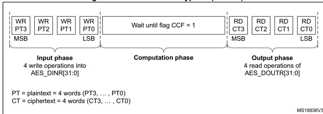
The diagram illustrates the ECB/CBC encryption sequence in Mode 1, divided into three phases:
- Input phase: Four write operations into the SAES_DINR register. The registers are labeled WR PT3, WR PT2, WR PT1, and WR PT0. PT3 is the MSB and PT0 is the LSB. The text below indicates: "Input phase 4 write operations into AES_DINR[31:0]".
- Computation phase: A central block labeled "Wait until flag CCF = 1". The text below indicates: "Computation phase".
- Output phase: Four read operations from the SAES_DOUTR register. The registers are labeled RD CT3, RD CT2, RD CT1, and RD CT0. CT3 is the MSB and CT0 is the LSB. The text below indicates: "Output phase 4 read operations of AES_DOUTR[31:0]".
Legend:
PT = plaintext = 4 words (PT3, ... , PT0)
CT = ciphertext = 4 words (CT3, ... , CT0)
MS18936V3
ECB/CBC decryption sequence
The sequence of events to perform an AES ECB/CBC decryption is as follows (More detail in Section 50.4.4 ). Select normal key mode by setting KMOD[1:0] to 00. For decryption with other KMOD[1:0] values, refer to Section 50.4.10 and Section 50.4.9 .
- 1. Follow the steps described in Section 50.4.5: SAES decryption round key preparation , in order to prepare the decryption key in AES core.
- 2. Select the Mode 3 by setting to 10 the MODE[1:0] bitfield of the SAES_CR register and select ECB or CBC chaining mode by setting the CHMOD[2:0] bitfield of the SAES_CR register to 000 or 001, respectively. Data type can also be defined, using DATATYPE[1:0] bitfield. KEYSIZE and KMOD[1:0] bitfields must be kept as-is.
- 3. Write the SAES_IVRx registers with the initialization vector (required in CBC mode only).
- 4. Enable SAES by setting the EN bit of the SAES_CR register.
- 5. Write the SAES_DINR register four times to input the cipher text (MSB first), as shown in Figure 494 .
- 6. Wait until the CCF flag is set in the SAES_SR register.
- 7. Read the SAES_DOUTR register four times to get the plain text (MSB first), as shown in Figure 494 . Then clear the CCF flag by setting the CCF bit of the SAES_ISR register.
- 8. Repeat steps 5-6-7 to process all the blocks encrypted with the same key.
Figure 494. ECB/CBC decryption (Mode 3)
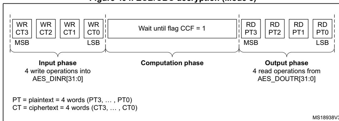
PT = plaintext = 4 words (PT3, ..., PT0)
CT = ciphertext = 4 words (CT3, ..., CT0)
MS18938V3
Suspend/resume operations in ECB/CBC modes
The following sequences are valid for normal key mode (KMOD[1:0] = 00).
To suspend the processing of a message , proceed as follows:
- 1. If DMA is used, stop the SAES DMA transfers to the IN FIFO by clearing the DMAINEN bit of the SAES_CR register.
- 2. If DMA is not used, read four times the SAES_DOUTR register to save the last processed block. If DMA is used, wait until the CCF flag is set in the SAES_SR register then stop the DMA transfers from the OUT FIFO by clearing the DMAOUTEN bit of the SAES_CR register.
- 3. If DMA is not used, poll the CCF flag of the SAES_SR register until it becomes 1 (computation completed).
- 4. Clear the CCF flag by setting the CCF bit of the SAES_ISR register.
- 5. Save initialization vector registers (only required in CBC mode as SAES_IVRx registers are altered during the data processing).
- 6. Disable the SAES peripheral by clearing the bit EN of the SAES_CR register.
- 7. Save the SAES_CR register and clear the key registers if they are not needed, to process the higher priority message.
- 8. If DMA is used, save the DMA controller status (pointers for IN and OUT data transfers, number of remaining bytes, and so on).
To resume the processing of a message, proceed as follows:
- 1. If DMA is used, configure the DMA controller so as to complete the rest of the FIFO IN and FIFO OUT transfers.
- 2. Disable the SAES peripheral by clearing the EN bit of the SAES_CR register.
- 3. Restore SAES_CR register (with correct KEYSIZE) then restore SAES_KEYRx registers. Alternatively, select a key source different from key registers, using KEYSEL[2:0]. Refer to Section 50.4.12: SAES key registers for details.
- 4. Prepare the decryption key as described in Section 50.4.5: SAES decryption round key preparation (only required for ECB or CBC decryption).
- 5. Restore SAES_IVRx registers using the saved configuration (only required in CBC mode).
- 6. Enable the SAES peripheral by setting the EN bit of the SAES_CR register.
- 7. If DMA is used, enable SAES DMA transfers by setting the DMAINEN and DMAOUTEN bits of the SAES_CR register.
50.4.9 SAES operation with wrapped keys
SAES peripheral can wrap (encrypt) and unwrap (decrypt) application keys using hardware-secret key DHUK, XOR-ed or not with application key BHK. With this feature, AES keys can be made usable by application software without being exposed in clear-text (unencrypted).
Wrapped key sequences are too small to be suspended/resumed. SAES cannot unwrap a key using an unwrapped key.
Figure 495 summarizes the operation with wrapped keys. To protect the wrapped key, select DHUK by setting KEYSEL[2:0] to 001 or 100. Alternatively, select BHK by setting KEYSEL to 010 if the corresponding registers are read/write-locked in the TAMP peripheral.
Figure 495. Operation with wrapped keys
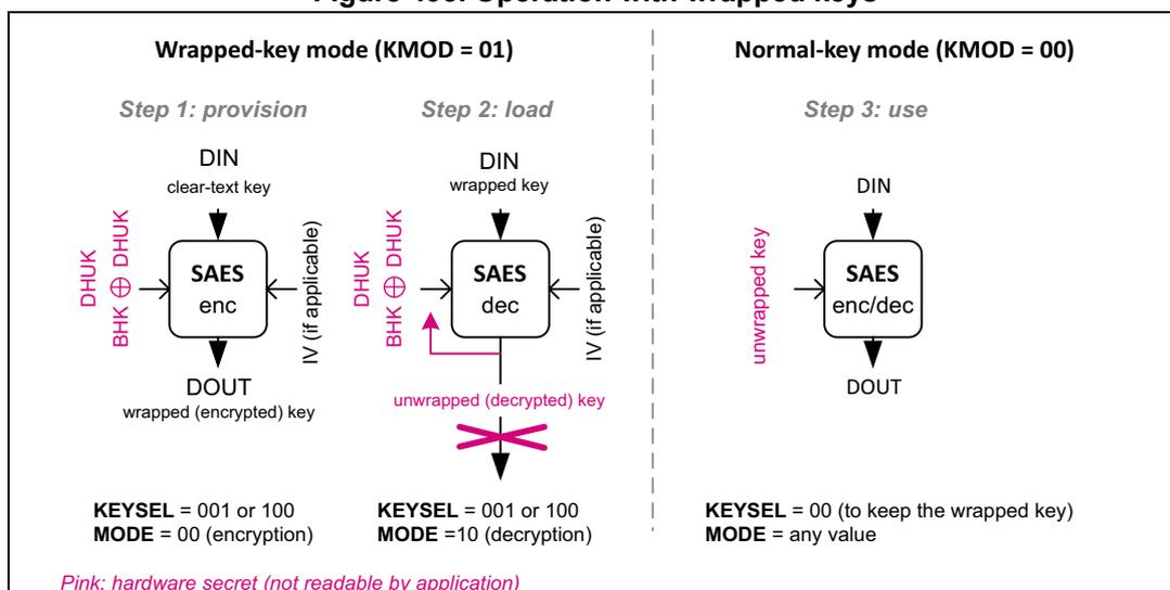
The diagram is divided into two main sections by a vertical dashed line.
- Wrapped-key mode (KMOD = 01)
:
- Step 1: provision : A clear-text key (DIN) is input to the SAES enc block. The block also receives a DHUK (BHK ⊕ DHUK) and an IV (if applicable). The output is a wrapped (encrypted) key (DOUT). Configuration: KEYSEL = 001 or 100, MODE = 00 (encryption).
- Step 2: load : A wrapped key (DIN) is input to the SAES dec block. The block also receives a DHUK (BHK ⊕ DHUK) and an IV (if applicable). The output is an unwrapped (decrypted) key (DOUT), which is shown with a large 'X' over it, indicating it is not readable. Configuration: KEYSEL = 001 or 100, MODE = 10 (decryption).
- Normal-key mode (KMOD = 00)
:
- Step 3: use : An unwrapped key (DIN) is input to the SAES enc/dec block. The output is DOUT. Configuration: KEYSEL = 00 (to keep the wrapped key), MODE = any value.
Pink: hardware secret (not readable by application)
Note: DHUK value depends on privilege, KMOD[1:0], KEYSEL, CHMOD[2:0], and on whether SAES peripheral is secure or nonsecure.
Encryption in Wrapped-key mode
Recommended sequence to wrap (that is, encrypt) a key is described below:
- Verify that BUSY = 0 in SAES_SR (no RNG random number fetch in progress).
- Disable the SAES peripheral by clearing the EN bit of the SAES_CR register.
- In SAES_CR register, select the Mode 1 (encryption) by setting to 00 the MODE[1:0] bitfield, and select ECB or CBC chaining mode by setting CHMOD[2:0] bitfield to 000 or 001, respectively. Data type can be defined as 32-bit, with DATATYPE[1:0] bitfield set to 00. Key size must be properly configured using KEYSIZE bit, and KMOD[1:0] bitfield must be set as 01 (wrapped key). The KEYSIZE information is used both for the encryption key and for the key to be encrypted.
- Write the SAES_IVRx registers with the initialization vector if CBC mode has been selected in previous step.
- Select the DHUK by setting the KEYSEL[2:0] bitfield of the SAES_CR register to 001 or 100. Upon successful key loading BUSY bit is cleared and KEYVALID bit is set in SAES_SR register. Refer to Section 50.4.12: SAES key registers for detail on KEYSEL = 100 usage.
- Enable SAES by setting the EN bit of the SAES_CR register.
- Write the SAES_DINR register four times to input the key to encrypt (MSB first, see Table 480 on page 1993 ).
- Wait until the CCF flag is set in the SAES_SR register.
- Get the encrypted key (MSB first) by reading the SAES_DOUTR register four times. Then clear the CCF flag by setting the CCF bit in SAES_ICR register.
- Repeat steps 6 to 8 if KEYSIZE is 256 bits.
Note: Encryption in Wrapped-key mode is only supported when ECB or CBC is selected through CHMOD[2:0].
Decryption in Wrapped-key mode
Recommended sequence to unwrap (i.e. decrypt) a wrapped key is described below:
- 1. Verify that BUSY = 0 in SAES_SR (no RNG random number fetch in progress).
- 2. Disable the SAES peripheral by clearing the EN bit of the SAES_CR register.
- 3. SAES_CR register, select the Mode 2 by setting to 01 the MODE[1:0] bitfield, and select ECB or CBC chaining mode by setting CHMOD[2:0] to 000 or 001, respectively. Key size must be properly configured using KEYSIZE bit, and KMOD[1:0] bitfield must be set as 01 (wrapped key). Data type selection with DATATYPE[1:0] bitfield must be the same as the one used during encryption (that is, 0x0). The KEYSIZE information is used both for the decryption key and for the key to be decrypted.
If the decrypted key is not to share with a different security context (different security attribute), the KEYPROT bit of the SAES_CR register must also be set.
- 4. Select the DHUK by setting the KEYSEL[2:0] bitfield of the SAES_CR register to 001 or 100. Upon successful key loading, the SAES_SR register BUSY bit is cleared and KEYVALID bit set. Refer to Section 50.4.12: SAES key registers for detail on KEYSEL = 100 usage.
- 5. Enable SAES by setting the EN bit of the SAES_CR register.
- 6. Wait until the CCF flag is set in the SAES_SR register.
- 7. Clear the CCF flag. Decryption key is available in AES core, and SAES is disabled automatically.
- 8. In SAES_CR register select the Mode 3 by setting to 10 the MODE[1:0] bitfield.
- 9. Write the SAES_IVRx registers with the initialization vector if CBC mode has been selected in previous step.
- 10. Enable SAES by setting the EN bit of the SAES_CR register.
- 11. Write the SAES_DINR register four times to input the encrypted random key (MSB first, see Table 480 on page 1993 ).
- 12. Wait until the CCF flag is set in the SAES_SR register.
- 13. Clear the CCF flag, then repeat steps 10 and 11 if KEYSIZE is 256 bits.
When the decrypted key is loaded in key registers, KEYSEL[2:0] of the SAES_CR register is automatically cleared. Hence, after this sequence, the decrypted wrapped key is available in SAES_KEYRx registers, immediately usable by the application software for any AES operation (normal key mode, that is, with KMOD[1:0] = 00).
Decrypted wrapped key can be shared with an application running in a different security context (different security attribute) if KEYPROT bit was cleared during step 2.
Note: When KMOD[1:0] = 01 (wrapped key) and MODE[1:0] = 10 (decryption) a read access to SAES_DOUTR register triggers a read error (RDERR).
When KEYSEL[2:0] = 001 (DHUK) or 100 (DHUK XOR BHK), the application software must use the same privilege, security, KMOD[1:0], CHMOD[2:0] and KEYSIZE context for encryption and decryption. Otherwise, the result is incorrect.
50.4.10 SAES operation with shared keys
SAES peripheral can share application keys wrapped with hardware-secret key DHUK, XOR-ed or not with application key BHK. With this feature, the application software can make the AES keys available to the AES peripheral, without exposing them in clear-text (unencrypted).
Shared key sequences are too small to be suspended/resumed. SAES cannot unwrap a shared key using an unwrapped key.
Note: When a key stored in SAES is shared with AES, the protection given by KEYPROT bit is lost. The protection is detailed in Section 50.4.12: SAES key registers .
Figure 496 summarizes how to use Shared-key mode. To protect the shared key, DHUK must be selected, by setting KEYSEL[2:0] to 001 or 100. Alternatively, select BHK by setting KEYSEL to 010 if the corresponding registers are read/write-locked in the TAMP peripheral.
Figure 496. Usage of Shared-key mode
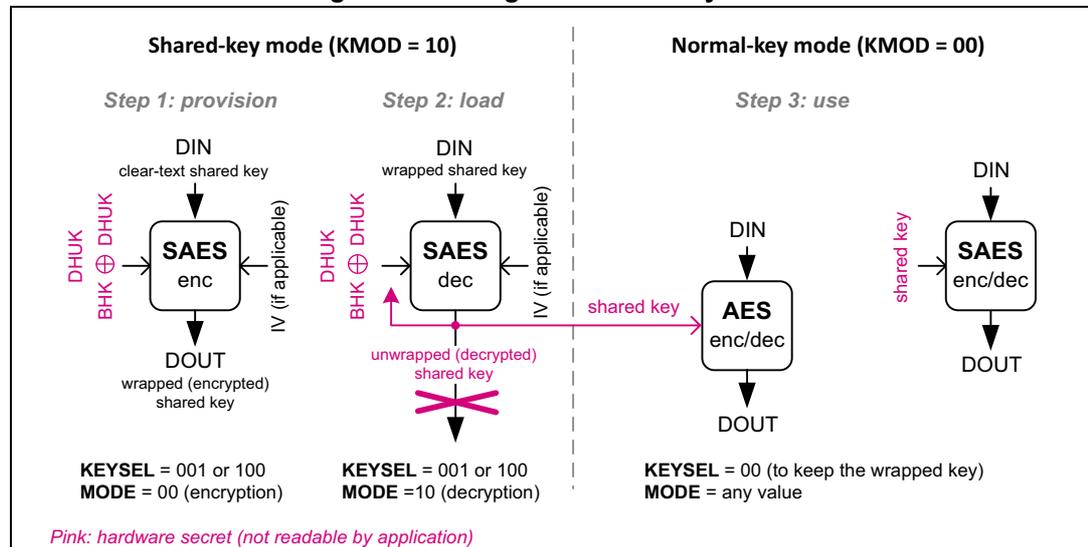
Shared-key mode (KMOD = 10)
Step 1: provision
DIN
clear-text shared key
↓
enc
↓
DOUT
wrapped (encrypted)
shared key
KEYSEL = 001 or 100
MODE = 00 (encryption)
Step 2: load
DIN
wrapped shared key
↓
dec
↓
unwrapped (decrypted)
shared key
KEYSEL = 001 or 100
MODE = 10 (decryption)
Normal-key mode (KMOD = 00)
Step 3: use
DIN
↓
enc/dec
↓
DOUT
DIN
↓
enc/dec
↓
DOUT
KEYSEL = 00 (to keep the wrapped key)
MODE = any value
Pink: hardware secret (not readable by application)
Note: DHUK value depends on privilege, KMOD[1:0], KSHAREID, KEYSEL, CHMOD[2:0], and on whether SAES peripheral is secure or nonsecure.
In the step 3, AES represents the AES peripheral.
Encryption in Shared-key mode
Before SAES can share a key with the AES peripheral, the key must be encrypted once. The encryption sequence of a shared key is the same as for a wrapped key, with KMOD[1:0] set to 10 (shared key) and KSHAREID[1:0] kept at 00 in the step 3 in Figure 496 . See Encryption in Wrapped-key mode for details.
Note: Encryption in Shared-key mode is only supported when ECB or CBC is selected through CHMOD[2:0].
Decryption in Shared-key mode
Each time SAES needs to share a key with the AES peripheral, shared encrypted key must be decrypted in SAES, then loaded by the AES. The overall sequence is described next.
Sequence in the SAES peripheral
The decryption sequence of a shared key is the same as for a wrapped key, with KMOD[1:0] set to 10 (shared key) and KSHAREID[1:0] kept at 00 in the step 3 in Figure 496 . See Decryption in Wrapped-key mode for details.
Note: Instead of being shared, a decrypted shared key can be used directly in SAES as the KEYSEL[2:0] bitfield is automatically cleared. In this case, KMOD[1:0] must be set to 00 (normal key mode).
Sequence in the AES peripheral
Once the shared key is decrypted in SAES key registers, it can be shared with the AES peripheral, while SAES peripheral remains in key sharing state, that is, with KMOD[1:0] = 10 and KEYVALID = 1 in the SAES_SR register. The sequence in the AES key share target peripheral is as follows:
- 1. Initialize the AES processor to process some data
- 2. When the key must be loaded, set the same KEYSIZE as for the SAES peripheral and write the KMOD[1:0] bitfield of the AES_CR register to 10 (shared key). If the previous sequence in the SAES peripheral completed successfully, with KMOD[1:0] kept at 10 and KSHAREID[1:0] kept at 00, the SAES_KEYRx registers are automatically copied into the AES_KEYRx registers, with BUSY set in AES_SR.
- 3. Once the transfer is completed, the BUSY flag is cleared and KEYVALID set in the AES_SR register. If KEYVALID is not set when BUSY bit is cleared, or if a key error flag (KEIF) is set an unexpected event occurred during the transfer, such as a DPA error, a tamper event or the KEYVALID SAES flag was cleared before the end of the transfer. When such errors occur, the whole key sharing process starting from the SAES peripheral must be restarted, through the IPRST bits of both control registers.
- 4. As KEYVALID is set, the key share target peripheral is initialized with a valid, shared key. The application can proceed with the data processing of data, setting KMOD[1:0] to 00.
This sequence can be run multiple times (for example, to manage a suspend/resume situation), as long as SAES is unused and duly remains in key sharing state.
Note: in SAES peripheral, when KMOD[1:0] = 10 (shared key) and MODE[1:0] = 10 (decryption), a read access to the SAES_DOUTR register triggers a read error (RDERR).
When KEYSEL[2:0] = 001 (DHUK) or 100 (DHUK XOR BHK), the application software must use the same privilege, security, KMOD[1:0] / KSHAREID[1:0], CHMOD[2:0], and KEYSIZE context for encryption and decryption. Otherwise, the result is incorrect.
When KMOD[1:0] = 10 and BUSY = 1 in the AES peripheral and KEYSIZE value of AES and SAES differs, the key sharing fails and the KEIF flag is raised in both peripherals.
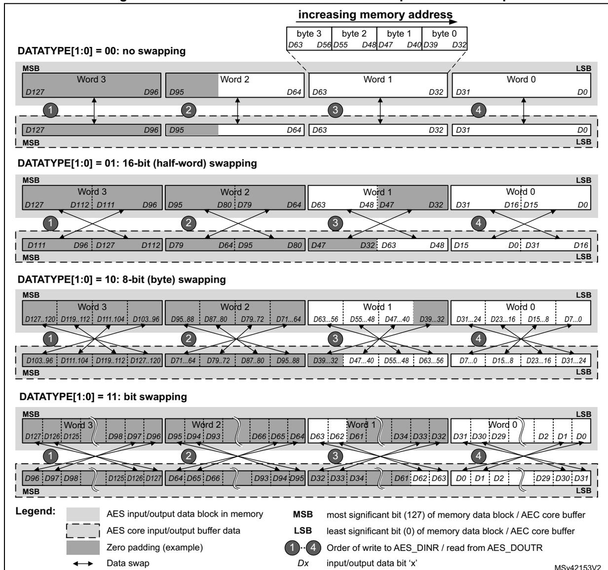
50.4.11 SAES data registers and data swapping
Data input and output
A 128-bit data block is entered into the SAES peripheral with four successive 32-bit word writes into the SAES_DINR register (bitfield DIN[31:0]), the most significant word (bits [127:96]) first, the least significant word (bits [31:0]) last.
A 128-bit data block is retrieved from the SAES peripheral with four successive 32-bit word reads from the SAES_DOUTR register (bitfield DOUT[31:0]), the most significant word (bits [127:96]) first, the least significant word (bits [31:0]) last.
The 32-bit data word for SAES_DINR register or from SAES_DOUTR register is organized in big endian order, that is:
- • the most significant byte of a word to write into SAES_DINR must be put on the lowest address out of the four adjacent memory locations keeping the word to write, or
- • the most significant byte of a word read from SAES_DOUTR goes to the lowest address out of the four adjacent memory locations receiving the word
For using DMA for input data block write into SAES, the four words of the input block must be stored in the memory consecutively and in big-endian order, that is, the most significant word on the lowest address. See Section 50.4.14: SAES DMA interface .
Data swapping
The SAES peripheral can be configured to perform a bit-, a byte-, a half-word-, or no swapping on the input data word in the SAES_DINR register, before loading it to the AES processing core, and on the data output from the AES processing core, before sending it to the SAES_DOUTR register. The choice depends on the type of data. For example, a byte swapping is used for an ASCII text stream.
The data swap type is selected through the DATATYPE[1:0] bitfield of the SAES_CR register. The selection applies both to the input and the output of the AES core.
For different data swap types, Figure 497 shows the construction of AES processing core input buffer data P127 to P0, from the input data entered through the SAES_DINR register, or the construction of the output data available through the SAES_DOUTR register, from the AES processing core output buffer data P127 to P0.
Figure 497. 128-bit block construction with respect to data swap
increasing memory address
byte 3 | byte 2 | byte 1 | byte 0
D63 D56 D55 D48 D47 D40 D39 D32
DATATYPE[1:0] = 00: no swapping
MSB Word 3 D127...D96 | Word 2 D95...D64 | Word 1 D63...D32 | Word 0 D31...D0 LSB
1 2 3 4
D127...D96 | D95...D64 | D63...D32 | D31...D0
MSB LSB
DATATYPE[1:0] = 01: 16-bit (half-word) swapping
MSB Word 3 D127...D112 | D111...D96 | Word 2 D95...D80 | D79...D64 | Word 1 D63...D48 | D47...D32 | Word 0 D31...D16 | D15...D0 LSB
1 2 3 4
D111...D96 | D127...D112 | D79...D64 | D95...D80 | D47...D32 | D63...D48 | D15...D0 | D31...D16
MSB LSB
DATATYPE[1:0] = 10: 8-bit (byte) swapping
MSB Word 3 D127...D120 | D119...D112 | D111...D104 | D103...D96 | Word 2 D95...D88 | D87...D80 | D79...D72 | D71...D64 | Word 1 D63...D56 | D55...D48 | D47...D40 | D39...D32 | Word 0 D31...D24 | D23...D16 | D15...D8 | D7...D0 LSB
1 2 3 4
D103...D96 | D111...D104 | D119...D112 | D127...D120 | D71...D64 | D79...D72 | D87...D80 | D95...D88 | D39...D32 | D47...D40 | D55...D48 | D63...D56 | D7...D0 | D15...D8 | D23...D16 | D31...D24
MSB LSB
DATATYPE[1:0] = 11: bit swapping
MSB Word 3 D127...D126 | D125...D98 | D97...D96 | Word 2 D95...D94 | D93...D66 | D65...D64 | Word 1 D63...D62 | D61...D34 | D33...D32 | Word 0 D31...D30 | D29...D2 | D1...D0 LSB
1 2 3 4
D96...D97...D98 | D125...D126...D127 | D64...D65...D66 | D93...D94...D95 | D32...D33...D34 | D61...D62...D63 | D0...D1...D2 | D29...D30...D31
MSB LSB
Legend:
- ■ AES input/output data block in memory
- □ AES core input/output buffer data
- ▒ Zero padding (example)
- ↔ Data swap
- MSB most significant bit (127) of memory data block / AES core buffer
- LSB least significant bit (0) of memory data block / AES core buffer
- ①...④ Order of write to AES_DINR / read from AES_DOUTR
- D x input/output data bit 'x'
MSv42153V2
Note: The data in SAES key registers (SAES_KEYRx) and initialization registers (SAES_IVRx) are not sensitive to the swap mode selection.
Data padding
Figure 497 also gives an example of memory data block padding with zeros such that the zeroed bits after the data swap form a contiguous zone at the MSB end of the AES core input buffer. The example shows the padding of an input data block containing:
- • 48 message bits, with DATATYPE[1:0] = 01
- • 56 message bits, with DATATYPE[1:0] = 10
- • 34 message bits, with DATATYPE[1:0] = 11
50.4.12 SAES key registers
The SAES_KEYRx write-only registers store the encryption or decryption key bitfield KEY[127:0] or KEY[255:0]. The data to write to each register is organized in the memory in little-endian order, that is, with most significant byte on the highest address (reads are not allowed for security reason).
The key is spread over eight registers as shown in Table 480 .
Table 480. Key endianness in SAES_KEYRx registers (128- or 256-bit key length)
| SAES_KEYR 7 [31:0] | SAES_KEYR 6 [31:0] | SAES_KEYR 5 [31:0] | SAES_KEYR 4 [31:0] | SAES_KEYR 3 [31:0] | SAES_KEYR 2 [31:0] | SAES_KEYR 1 [31:0] | SAES_KEYR 0 [31:0] |
|---|---|---|---|---|---|---|---|
| - | - | - | - | KEY[127:96] | KEY[95:64] | KEY[63:32] | KEY[31:0] |
| KEY[255:224] | KEY[223:192] | KEY[191:160] | KEY[159:128] | KEY[127:96] | KEY[95:64] | KEY[63:32] | KEY[31:0] |
| TAMP_BKP7R [31:0] | TAMP_BKP6R [31:0] | TAMP_BKP5R [31:0] | TAMP_BKP4R [31:0] | TAMP_BKP3R [31:0] | TAMP_BKP2R [31:0] | TAMP_BKP1R [31:0] | TAMP_BKP0R [31:0] |
The key for encryption or decryption may be written into these registers when the SAES peripheral is disabled, by clearing the EN bit and the KEYSEL[2:0] bitfield of the SAES_CR register.
The key registers are not affected by the data swapping controlled by DATATYPE[1:0] bitfield of the SAES_CR register.
The entire key must be written before starting an AES computation. In normal key mode (KMOD[1:0] = 00), with KEYSEL[2:0] = 000, the SAES_KEYRx (x = 0 to 3 for KEYSIZE = 0, x = 0 to 7 for KEYSIZE = 1) registers must always be written in either ascending or descending order.
With KEYSEL[2:0] set to 001, a derived hardware unique key (DHUK), computed inside the SAES engine from a non-volatile OTP-based root hardware unique key, is loaded directly into key registers, based on KEYSIZE information.
With KEYSEL[2:0] set to 010, the boot hardware key (BHK), stored in tamper-resistant secure backup registers, is entirely transferred into key registers upon a secure application performing a single read of all TAMP_BKPxR registers (x = 0 to 3 for KEYSIZE = 0, x = 0 to 7 for KEYSIZE = 1) in either ascending or descending order. Refer to Table 480 .
With KEYSEL[2:0] set to 100, the XOR combination of DHUK and BHK is entirely transferred into key registers upon a secure application performing a single read of all TAMP_BKPxR registers (x = 0 to 3 for KEYSIZE = 0, x = 0 to 7 for KEYSIZE = 1) in either ascending or descending order. Refer to Table 480 .
Repeated writing of KEYSEL[2:0] with the same non-zero value only triggers the loading of DHUK or BHK if KEYVALID = 0. The recommended method to clear KEYVALID is to set the IPRST bit in the SAES_CR register. Such method is required for example when switching from ECB decryption to ECB encryption, selecting the same BHK (KEYSEL[2:0] = 010).
The KEYPROT bit of SAES_CR register must be set if the key to load in key registers must not be shared with an application executing in a different security context (that is, different security attribute). Setting KEYPROT and KEYVALID makes KEIF flag an error upon SAES access attempts by an application executing in a different security context than the one that loaded the key, as shown in Figure 498.
Note: KEYSEL[2:0] values different from zero (normal key) automatically protect the key registers.
DHUK, BHK and their XOR combination are not readable by any software (even secure).
Secure SAES uses secure DHUK. Nonsecure SAES uses nonsecure DHUK.
Figure 498. Key protection mechanisms
![Diagram illustrating key protection mechanisms in SAES. It shows two security contexts: Security context A (secure) and Security context B (nonsecure). In context A, the SAES block has a key icon and is labeled with KEYVALID = 1. In context B, there are two SAES blocks. The top one is labeled with KEYPROT = 0 and KEYSEL[2:0] = 000. The bottom one is labeled with KEYPROT = 1 or KEYSEL ≠ 000 and has a crossed-out key icon, with a lightning bolt labeled KEIF indicating an error. Arrows point from the text labels to the corresponding SAES blocks. The diagram is labeled MSv63151V1 in the bottom right corner.](/RM0456-STM32U5/c2838cb7f48d738579cc2d44d0260547_img.jpg)
Note: Initiating the key-loading sequence sets the BUSY flag and clears the KEYVALID flag. Once the amount of bits defined by KEYSIZE is transferred to the SAES_KEYRx registers, BUSY is cleared, KEYVALID set and the EN bit becomes writable. If an error occurs, BUSY and KEYVALID are cleared and KEIF set (see Section 50.4.15: SAES error management for details). This holds for all KEYSEL values. For additional information on key modes, refer to Section 50.4.10 and Section 50.4.9 .
50.4.13 SAES initialization vector registers
The four SAES_IVRx registers keep the initialization vector input bitfield IVI[127:0]. The data to write to or to read from each register is organized in the memory in little-endian order, that is, with most significant byte on the highest address. The registers are also ordered from lowest address (SAES_IVR0) to highest address (SAES_IVR3).
The signification of data in the bitfield depends on the chaining mode selected. When used, the bitfield is updated upon each computation cycle of the AES core.
Write operations to the SAES_IVRx registers when the SAES peripheral is enabled have no effect to the register contents. For modifying the contents of the SAES_IVRx registers, the EN bit of the SAES_CR register must first be cleared.
Reading the SAES_IVRx registers returns the latest counter value (useful for managing suspend mode).
The SAES_IVRx registers are not affected by the data swapping feature controlled by the DATATYPE[1:0] bitfield of the SAES_CR register.
50.4.14 SAES DMA interface
The SAES peripheral provides an interface to connect to the DMA (direct memory access) controller. The DMA operation is controlled through the SAES_CR register.
Data input using DMA
Setting the DMAINEN bit of the SAES_CR register enables DMA writing into SAES. The SAES peripheral then initiates a DMA request during the input phase each time it requires to write a 128-bit block (quadruple word) to the SAES_DINR register, as shown in Figure 499 .
Note: According to the algorithm and the mode selected, special padding / ciphertext stealing might be required. For details, refer to Section 50.4.6: SAES ciphertext stealing and data padding .
Figure 499. DMA transfer of a 128-bit data block during input phase
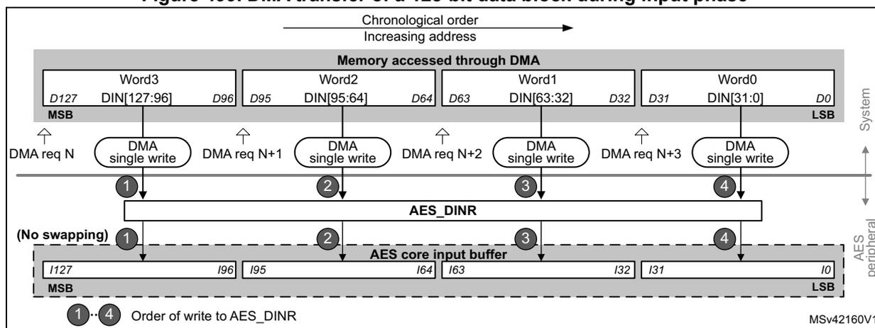
The diagram illustrates the DMA transfer of a 128-bit data block during the input phase. At the top, a horizontal arrow indicates 'Chronological order' and 'Increasing address'. Below this, a section titled 'Memory accessed through DMA' shows four words: Word3 (D127 to D96), Word2 (D95 to D64), Word1 (D63 to D32), and Word0 (D31 to D0). Each word is associated with a 'DMA single write' operation, labeled 'DMA req N', 'DMA req N+1', 'DMA req N+2', and 'DMA req N+3' respectively. Arrows show the data flow from these writes into the 'AES_DINR' register. From the AES_DINR register, four arrows labeled 1, 2, 3, and 4 show the data being transferred into the 'AES core input buffer'. A note '(No swapping)' is present. The input buffer is shown as a 128-bit wide register with bits labeled from 127 down to 0, with MSB at bit 127 and LSB at bit 0. At the bottom, a sequence of four circles labeled 1 to 4 indicates the 'Order of write to AES_DINR'. The diagram is labeled 'MSv42160V1' in the bottom right corner.
Data output using DMA
Setting the DMAOUTEN bit of the SAES_CR register enables DMA reading from SAES. The SAES peripheral then initiates a DMA request during the Output phase each time it requires to read a 128-bit block (quadruple word) to the SAES_DINR register, as shown in Figure 500 .
Note: According to the message size, extra bytes might need to be discarded by application in the last block.
Figure 500. DMA transfer of a 128-bit data block during output phase
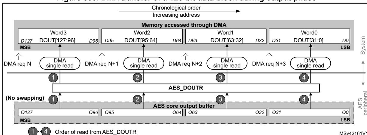
The diagram illustrates the data flow during the output phase of a DMA transfer for a 128-bit data block. At the top, a horizontal arrow indicates 'Chronological order' and 'Increasing address' from left to right. Below this, a section titled 'Memory accessed through DMA' shows four 32-bit words: Word3 (bits D127 to D96), Word2 (bits D95 to D64), Word1 (bits D63 to D32), and Word0 (bits D31 to D0). Each word is associated with a 'DMA single read' request, labeled DMA req N, DMA req N+1, DMA req N+2, and DMA req N+3 respectively. These requests are shown as arrows pointing from the DMA controller to the memory. Below the memory section is the 'AES_DOUTR' register. Four arrows, numbered 1 to 4 in circles, point from the AES_DOUTR register to the memory words. Below the AES_DOUTR register is the 'AES core output buffer', which contains 128 bits (O127 to O0). Four arrows, also numbered 1 to 4 in circles, point from the output buffer to the AES_DOUTR register. A label '(No swapping)' is present next to the first arrow. At the bottom, a legend shows four circled numbers 1 to 4 with the text 'Order of read from AES_DOUTR'. The right side of the diagram is labeled 'System' and 'AES peripheral'. The identifier 'MSV42161V1' is in the bottom right corner.
DMA operation in different operating modes
DMA operations are usable when Mode 1 (encryption) or Mode 3 (decryption) are selected via the MODE[1:0] bitfield of the register SAES_CR. As in Mode 2 (key derivation) the SAES_KEYRx registers must be written by software, enabling the DMA transfer through the DMAINEN and DMAOUTEN bits of the SAES_CR register have no effect in that mode.
DMA single requests are generated by SAES until it is disabled. So, after the data output phase at the end of processing of a 128-bit data block, SAES switches automatically to a new data input phase for the next data block, if any.
When the data transferring between SAES and memory is managed by DMA, the CCF flag has no use because the reading of the SAES_DOUTR register is managed by DMA automatically at the end of the computation phase. The CCF flag must only be cleared when transiting back to data transferring managed by software. See Section 50.4.4: SAES procedure to perform a cipher operation , subsection Data append , for details.
50.4.15 SAES error management
Unless indicated otherwise, SAES configuration can be changed at any moment by clearing the EN bit of the SAES_CR register.
Read error flag (RDERR)
Unexpected read attempt of the SAES_DOUTR register sets the RDERR flag of the SAES_SR register and the RWEIF flag of the SAES_ISR register, and returns zero.
RDERR is triggered during the computation phase or during the input phase.
Note: Unless indicated otherwise, SAES is not disabled upon a RDERR error detection and continues processing.
An interrupt is generated if the RWEIE bit of the SAES_IER register is set. For more details, refer to Section 50.5: SAES interrupts .
The RDERR and RWEIF flag is cleared by setting the RWEIE bit of the SAES_ISR register.
Write error flag (WDERR)
Unexpected write attempt of the SAES_DINR register sets the WDERR flag of the SAES_SR register and the RWEIF flag of the SAES_ISR register, and has no effect on the
SAES_DINR register. The WRERR is triggered during the computation phase or during the output phase.
Note: Unless indicated otherwise, SAES is not disabled after a WRERR error detection and continues processing.
An interrupt is generated if the RWEIE bit of the SAES_IER register is set. For more details, refer to Section 50.5: SAES interrupts .
The WRERR and RWEIF flag is cleared by setting the RWEIF bit of the SAES_ISR register.
Key error interrupt flag (KEIF)
Failure to load a key into key registers, or attempt to load a key while the key is protected, sets the KEIF flag of the SAES_ISR register and clears the KEYVALID bit of the SAES_SR register.
The KEIF flag is cleared with corresponding bit of the SAES_ISR register. An interrupt is generated if the KEIE bit of the SAES_IER register is set. For more details, refer to Section 50.5: SAES interrupts .
The possible sources of key errors are:
- • Key protection error: while KEYVALID is set, if KEYPROT = 1 or KEYSEL is different from zero this error is triggered when an application executing in a security context different from the one used to load the key is detected accessing the SAES (that is, different security attribute).
- • Key writing sequence error: an incorrect sequence has been detected when writing key registers. See Section 50.4.12: SAES key registers for details.
- • Key sharing size mismatch: error is triggered when KMOD[1:0] = 10 and application sets a KEYSIZE information in AES peripheral that does not match the KEYSIZE stored in SAES peripheral
- • Key sharing error: the copy of key registers from SAES peripheral to AES failed. See Section 50.4.10: SAES operation with shared keys for details.
- • Hardware secret key loading error: the DHUK or BHK failed to load into SAES. KEYSEL = 001 (DHUK), 010 (BHK) or 100 (DHUK XOR BHK) is not functional.
Upon a key sharing error, reset both AES and SAES peripherals through the IPRST bit of their corresponding control register, then restart the key sharing sequence.
Upon a key selection error, clearing the KEIF flag automatically restarts the key selection process. Persisting problems (for example, RHUK load failing) may require a power-on reset.
Note: For any key error, clear KEIF flag prior to re-configuring SAES.
RNG error interrupt flag (RNGEIF)
SAES fetches random numbers from the RNG peripheral automatically after an IP reset triggered in the RCC. SAES cannot be used when RNGEIF is set.
An error detected while fetching a random number from RNG peripheral (due to, for example, bad entropy) sets the RNGEIF flag of the SAES_ISR register. The flag is cleared by setting the corresponding bit of the SAES_ICR register. An interrupt is generated if the
RNGEIE bit of the SAES_IER register is set. For more details, refer to Section 50.5: SAES interrupts .
Upon an RNG error:
- • Verify that the RNG peripheral AHB clock is enabled and no noise source (or seed) error is pending in this peripheral.
- • Clear the RNGEIF bit of the SAES_ISR register, or reset the peripheral by setting the IPRST bit of the SAES_CR register. The clearance of the BUSY flag in the SAES_SR register then indicates the completion of the random number fetch from RNG.
Note: To avoid RNGEIF errors, it is recommended to activate the RNG AHB clock each time SAES AHB clock is activated.
About DPA errors
An unexpected error triggers an SAES internal tamper event in the TAMP peripheral, and stops any SAES co-processor processing.
To resume normal operation, application must reset the SAES peripheral through RCC or global reset.
50.5 SAES interrupts
Individual maskable interrupt sources generated by the SAES peripheral signal the following events:
- • computation completed
- • read error
- • write error
- • key error
- • RNG error
These sources are combined into a common interrupt signal from the SAES peripheral that connects to the Arm ® Cortex ® interrupt controller. Each can individually be enabled/disabled, by setting/clearing the corresponding enable bit of the SAES_IER register, and cleared by setting the corresponding bit of the SAES_ISR register.
The status of each can be read from the SAES_SR and SAES_ISR registers.
Table 481 gives a summary of the interrupt sources, their event flags and enable bits.
Table 481. SAES interrupt requests
| Interrupt acronym | SAES interrupt event | Event flag | Enable bit | Interrupt clear method |
|---|---|---|---|---|
| SAES | computation completed flag | CCF | CCFIE | set CCF (1) |
| read error flag | RDERR (2) | RWEIE | set RWEIF (1) | |
| write error flag | WRERR (2) | |||
| key error flag | KEIF | KEIE | set KEIF (1) | |
| RNG error flag | RNGEIF | RNGEIE | set RNGEIF (1) |
1. Bit of the SAES_ISR register.
2. Flag of the SAES_SR register, mirrored by the flag RWEIF of the SAES_ISR register.
50.6 SAES processing latency
The tables below summarize the latency to process a 128-bit block for each mode of operation.
Table 482. Processing latency for ECB, CBC
| Key size | Mode of operation | Algorithm | Clock cycles (1) |
|---|---|---|---|
| 128-bit | Mode 1: Encryption | ECB, CBC | 528 |
| Mode 2: Key derivation | - | 200 | |
| Mode 3: Decryption | ECB, CBC | 528 | |
| 256-bit | Mode 1: Encryption | ECB, CBC | 743 |
| Mode 2: Key derivation | - | 324 | |
| Mode 3: Decryption | ECB, CBC | 743 |
1. SHSI clock from RCC (48 MHz with +/-15% jitter)
50.7 SAES registers
50.7.1 SAES control register (SAES_CR)
Address offset: 0x00
Reset value: 0x0000 0000
| 31 | 30 | 29 | 28 | 27 | 26 | 25 | 24 | 23 | 22 | 21 | 20 | 19 | 18 | 17 | 16 |
|---|---|---|---|---|---|---|---|---|---|---|---|---|---|---|---|
| IPRST | KEYSEL[2:0] | KSHAREID[1:0] | KMOD[1:0] | Res. | KEYPROT | KEYSIZE | Res. | CHMOD[2] | |||||||
| rw | rw | rw | rw | rw | rw | rw | rw | rw | rw | rw | |||||
| 15 | 14 | 13 | 12 | 11 | 10 | 9 | 8 | 7 | 6 | 5 | 4 | 3 | 2 | 1 | 0 |
| Res. | DMAOUTEN | DMAINEN | Res. | Res. | CHMOD[1:0] | MODE[1:0] | DATATYPE[1:0] | EN | |||||||
| rw | rw | rw | rw | rw | rw | rw | rw | rw | |||||||
Bit 31 IPRST : SAES peripheral software reset
Setting the bit resets the SAES peripheral, putting all registers to their default values, except the IPRST bit itself and the SAES_DPACFG register. Hence, any key-relative data is lost. For this reason, it is recommended to set the bit before handing over the SAES to a less secure application. The bit must be low while writing any configuration registers.
Bits 30:28 KEYSEL[2:0] : Key selectionThe bitfield defines the source of the key information to use in the AES cryptographic core.
- 000: Software key, loaded in key registers SAES_KEYx
- 001: Derived hardware unique key (DHUK)
- 010: Boot hardware key (BHK)
- 100: XOR of DHUK and BHK
- 111: Test mode key (256-bit hardware constant 0xA5A5...A5A5)
- Others: Reserved (if used, unfreeze SAES with IPRST)
When KEYSEL is different from zero, selected key value is available in key registers when BUSY bit is cleared and KEYVALID is set in the SAES_SR register. Otherwise, the key error flag KEIF is set. Repeated writing of KEYSEL[2:0] with the same non-zero value only triggers the loading of DHUK or BHK if KEYVALID = 0.
When the application software changes the key selection by writing the KEYSEL[2:0] bitfield, the key registers are immediately erased and the KEYVALID flag cleared.
At the end of the decryption process, if KMOD[1:0] is other than zero, KEYSEL[2:0] is cleared.
With the bitfield value other than zero and KEYVALID set, the application cannot transfer the ownership of SAES with a loaded key to an application running in another security context (such as secure, nonsecure). More specifically, when security of an access to any register does not match the information recorded by SAES, the KEIF flag is set.
Attempts to write the bitfield are ignored when the BUSY flag of SAES_SR register is set, as well as when the EN bit of the SAES_CR register is set before the write access and it is not cleared by that write access.
Bits 27:26 KSHAREID[1:0] : Key share identificationThis bitfield defines, at the end of a decryption process with KMOD[1:0] = 10 (shared key), which target can read the SAES key registers using a dedicated hardware bus.
- 00: AES peripheral
- Others: Reserved
Attempts to write the bitfield are ignored when the BUSY flag of SAES_SR register is set, as well as when the EN bit of the SAES_CR register is set before the write access and it is not cleared by that write access.
Bits 25:24 KMOD[1:0] : Key mode selectionThe bitfield defines how the SAES key can be used by the application:
- 00: Normal key
- 01: Wrapped key
- 10: Shared key
- Others: Reserved
With normal key selection, the key registers are freely usable, no specific usage or protection applies to SAES_DIN and SAES_DOUT registers.
With wrapped key selection, the key loaded in key registers can only be used to encrypt or decrypt AES keys. Hence, when a decryption is selected in Wrapped-key mode read-as-zero SAES_DOUT register is automatically loaded into SAES key registers after a successful decryption process.
With shared key selection, after a successful decryption process, SAES key registers are shared with the peripheral described in KSHAREID[1:0] bitfield. This sharing is valid only while KMOD[1:0] = 10 and KEYVALID = 1. When a decryption is selected, read-as-zero SAES_DOUT register is automatically loaded into SAES key registers after a successful decryption process.
With KMOD[1:0] other than zero, any attempt to configure the SAES peripheral for use by an application belonging to a different security domain (secure or nonsecure) results in automatic key erasure and setting of the KEIF flag.
Attempts to write the bitfield are ignored when the BUSY flag of SAES_SR register is set, as well as when the EN bit of the SAES_CR register is set before the write access and it is not cleared by that write access.
Bits 23:20 Reserved, must be kept at reset value.
Bit 19 KEYPROT: Key protectionWhen set, hardware-based key protection is enabled.
0: When KEYVALID is set and KEYSEL = 0 application can transfer the ownership of the SAES, with its loaded key, to an application running in another security context (such as nonsecure, secure).
1: When KEYVALID is set, key error flag (KEIF) is set when an access to any registers is detected, this access having a security context (for example, secure, nonsecure) that does not match the one of the application that loaded the key.
Attempts to write the bit are ignored when the BUSY flag of SAES_SR register is set, as well as when the EN bit of the SAES_CR register is set before the write access and it is not cleared by that write access.
Bit 18 KEYSIZE: Key size selectionThis bitfield defines the length of the key used in the SAES cryptographic core, in bits:
0: 128
1: 256
When KMOD[1:0] = 01 or 10 KEYSIZE also defines the length of the key to encrypt or decrypt.
Attempts to write the bit are ignored when the BUSY flag of SAES_SR register is set, as well as when the EN bit of the SAES_CR register is set before the write access and it is not cleared by that write access.
Bit 17 Reserved, must be kept at reset value.
Bit 16 Reserved, must be kept at reset value.
Bits 15:13 Reserved, must be kept at reset value.
Bit 12 DMAOUTEN: DMA output enableThis bit enables/disables data transferring with DMA, in the output phase:
0: Disable
1: Enable
When the bit is set, DMA requests are automatically generated by SAES during the output data phase. This feature is only effective when Mode 1 or Mode 3 is selected through the MODE[1:0] bitfield. It is not effective for Mode 2 (key derivation).
Bit 11 DMAINEN: DMA input enableThis bit enables/disables data transferring with DMA, in the input phase:
0: Disable
1: Enable
When the bit is set, DMA requests are automatically generated by SAES during the input data phase. This feature is only effective when Mode 1 or Mode 3 is selected through the MODE[1:0] bitfield. It is not effective for Mode 2 (key derivation).
Bits 10:7 Reserved, must be kept at reset value.
Bit 6 Reserved, must be kept at reset value.
Bits 16, 6:5 CHMOD[2:0]: Chaining mode selectionThis bitfield selects the AES chaining mode:
000: Electronic codebook (ECB)
001: Cipher-block chaining (CBC)
others: Reserved
Attempts to write the bitfield are ignored when the BUSY flag of SAES_SR register is set, as well as when the EN bit of the SAES_CR register is set before the write access and it is not cleared by that write access.
Bits 4:3 MODE[1:0] : SAES operating mode
This bitfield selects the SAES operating mode:
00: Mode 1: encryption
01: Mode 2: key derivation (or key preparation for ECB/CBC decryption)
10: Mode 3: decryption
11: Reserved
Attempts to write the bitfield are ignored when the BUSY flag of SAES_SR register is set, as well as when the EN bit of the SAES_CR register is set before the write access and it is not cleared by that write access.
Bits 2:1 DATATYPE[1:0] : Data type selection
This bitfield defines the format of data written in the SAES_DINR register or read from the SAES_DOUTR register, through selecting the mode of data swapping:
00: None
01: Half-word (16-bit)
10: Byte (8-bit)
11: Bit
For more details, refer to Section 50.4.11: SAES data registers and data swapping .
Attempts to write the bitfield are ignored when the BUSY flag of SAES_SR register is set, as well as when the EN bit of the SAES_CR register is set before the write access and it is not cleared by that write access.
Bit 0 EN : SAES enable
This bit enables/disables the SAES peripheral:
0: Disable
1: Enable
At any moment, clearing then setting the bit re-initializes the SAES peripheral.
This bit is automatically cleared by hardware upon the completion of the key preparation (Mode 2) .
The bit cannot be set as long as KEYVALID = 0.
Note: With KMOD[1:0] other than 00, use the IPRST bit rather than the bit EN.
50.7.2 SAES status register (SAES_SR)
Address offset: 0x04
Reset value: 0x0000 0000
| 31 | 30 | 29 | 28 | 27 | 26 | 25 | 24 | 23 | 22 | 21 | 20 | 19 | 18 | 17 | 16 |
|---|---|---|---|---|---|---|---|---|---|---|---|---|---|---|---|
| Res. | Res. | Res. | Res. | Res. | Res. | Res. | Res. | Res. | Res. | Res. | Res. | Res. | Res. | Res. | Res. |
| 15 | 14 | 13 | 12 | 11 | 10 | 9 | 8 | 7 | 6 | 5 | 4 | 3 | 2 | 1 | 0 |
| Res. | Res. | Res. | Res. | Res. | Res. | Res. | Res. | KEYVALID | Res. | Res. | Res. | BUSY | WRERR | RDERR | CCF |
| r | r | r | r | r |
Bits 31:8 Reserved, must be kept at reset value.
Bit 7 KEYVALID: Key Valid flagThis bit is set by hardware when the amount of key information defined by KEYSIZE in SAES_CR has been loaded in SAES_KEYYx key registers.
0: No valid key information is available in key registers. EN bit in SAES_CR cannot be set.
1: Valid key information, defined by KEYSIZE in SAES_CR, is loaded in key registers.
In normal mode when KEYSEL equals to zero, the application must write the key registers in the correct sequence, otherwise the KEIF flag of the SAES_ISR register is set and KEYVALID stays at zero.
When KEYSEL is different from zero the BUSY flag is automatically set by SAES. When key is loaded successfully, the BUSY flag is cleared and KEYVALID set. Upon an error, the KEIF flag of the SAES_ISR register is set, the BUSY flag cleared and KEYVALID kept at zero.
When the KEIF flag is set, the application must clear it through the SAES_ICR register, otherwise KEYVALID cannot be set. See the KEIF bit description for more details.
For more information on key loading, refer to Section 50.4.12: SAES key registers .
Bits 6:4 Reserved, must be kept at reset value.
Bit 3 BUSY: BusyThis flag indicates whether SAES is idle or busy during GCM payload encryption phase:
0: Idle
1: Busy
The flag is also set upon SAES initialization, upon fetching random number from the RNG, or upon transferring a shared key to a target peripheral.
Bit 2 WRERR: Write errorThis flag indicates the detection of an unexpected write operation to the SAES_DINR register (during computation or data output phase):
0: Not detected
1: Detected
The flag is set by hardware. It is cleared by software upon setting the RWEIF bit of the SAES_ISR register.
Upon the flag setting, an interrupt is generated if enabled through the RWEIE bit of the SAES_ISR register.
The flag setting has no impact on the SAES operation. Unexpected write is ignored.
Bit 1 RDERR: Read error flagThis flag indicates the detection of an unexpected read operation from the SAES_DOUTR register (during computation or data input phase):
0: Not detected
1: Detected
The flag is set by hardware. It is cleared by software upon setting the RWEIF bit of the SAES_ISR register.
Upon the flag setting, an interrupt is generated if enabled through the RWEIE bit of the SAES_ISR register.
The flag setting has no impact on the SAES operation. Unexpected read returns zero.
Bit 0 CCF: Computation completed flagThis bit mirrors the CCF bit of the SAES_ISR register.
50.7.3 SAES data input register (SAES_DINR)
Address offset: 0x08
Reset value: 0x0000 0000
Only 32-bit write access type is supported.
| 31 | 30 | 29 | 28 | 27 | 26 | 25 | 24 | 23 | 22 | 21 | 20 | 19 | 18 | 17 | 16 |
| DIN[31:16] | |||||||||||||||
| w | w | w | w | w | w | w | w | w | w | w | w | w | w | w | w |
| 15 | 14 | 13 | 12 | 11 | 10 | 9 | 8 | 7 | 6 | 5 | 4 | 3 | 2 | 1 | 0 |
| DIN[15:0] | |||||||||||||||
| w | w | w | w | w | w | w | w | w | w | w | w | w | w | w | w |
Bits 31:0 DIN[31:0] : Input data word
A four-fold sequential write to this bitfield during the input phase results in writing a complete 128-bit block of input data to the SAES peripheral. From the first to the fourth write, the corresponding data weights are [127:96], [95:64], [63:32], and [31:0]. Upon each write, the data from the 32-bit input buffer are handled by the data swap block according to the DATATYPE[1:0] bitfield, then written into the AES core 128-bit input buffer.
The data signification of the input data block depends on the SAES operating mode:
- - Mode 1 (encryption): plaintext
- - Mode 2 (key derivation): the bitfield is not used (SAES_KEYRx registers used for input if KEYSEL = 0)
- - Mode 3 (decryption): ciphertext
The data swap operation is described in Section 50.4.11: SAES data registers and data swapping on page 1991 .
50.7.4 SAES data output register (SAES_DOUTR)
Address offset: 0x0C
Reset value: 0x0000 0000
Only 32-bit read access type is supported. Read when KMOD[1:0] = 01 or 10 while MODE[1:0] = 10 and EN = 1 triggers a read error.
| 31 | 30 | 29 | 28 | 27 | 26 | 25 | 24 | 23 | 22 | 21 | 20 | 19 | 18 | 17 | 16 |
| DOUT[31:16] | |||||||||||||||
| r | r | r | r | r | r | r | r | r | r | r | r | r | r | r | r |
| 15 | 14 | 13 | 12 | 11 | 10 | 9 | 8 | 7 | 6 | 5 | 4 | 3 | 2 | 1 | 0 |
| DOUT[15:0] | |||||||||||||||
| r | r | r | r | r | r | r | r | r | r | r | r | r | r | r | r |
Bits 31:0 DOUT[31:0] : Output data word
This read-only bitfield fetches a 32-bit output buffer. A four-fold sequential read of this bitfield, upon the computation completion (CCF set), virtually reads a complete 128-bit block of output data from the SAES peripheral. Before reaching the output buffer, the data produced by the AES core are handled by the data swap block according to the DATATYPE[1:0] bitfield.
Data weights from the first to the fourth read operation are: [127:96], [95:64], [63:32], and [31:0].
The data signification of the output data block depends on the SAES operating mode:
- - Mode 1 (encryption): ciphertext
- - Mode 2 (key derivation): the bitfield is not used
- - Mode 3 (decryption): plaintext
The data swap operation is described in Section 50.4.11: SAES data registers and data swapping on page 1991 .
50.7.5 SAES key register 0 (SAES_KEYR0)
Address offset: 0x10
Reset value: 0x0000 0000
| 31 | 30 | 29 | 28 | 27 | 26 | 25 | 24 | 23 | 22 | 21 | 20 | 19 | 18 | 17 | 16 |
|---|---|---|---|---|---|---|---|---|---|---|---|---|---|---|---|
| KEY[31:16] | |||||||||||||||
| w | w | w | w | w | w | w | w | w | w | w | w | w | w | w | w |
| 15 | 14 | 13 | 12 | 11 | 10 | 9 | 8 | 7 | 6 | 5 | 4 | 3 | 2 | 1 | 0 |
| KEY[15:0] | |||||||||||||||
| w | w | w | w | w | w | w | w | w | w | w | w | w | w | w | w |
Bits 31:0 KEY[31:0] : Cryptographic key, bits [31:0]
This write-only bitfield contains the bits [31:0] of the AES encryption or decryption key, depending on the operating mode:
- - In Mode 1 (encryption), Mode 2 (key derivation): the value to write into the bitfield is the encryption key.
- - In Mode 3 (decryption): the value to write into the bitfield is the encryption key to be derived before being used for decryption.
The SAES_KEYRx registers may be written only when KEYSIZE value is correct and when the SAES peripheral is disabled (EN bit of the SAES_CR register cleared). A special writing sequence is also required, as described in KEYVALID bit of the SAES_SR register. Note that, if KEYSEL is different from 0 and KEYVALID = 0, the key is directly loaded to SAES_KEYRx registers (hence writes to key register is ignored and KEIF is set).
Refer to Section 50.4.12: SAES key registers on page 1993 for more details.
50.7.6 SAES key register 1 (SAES_KEYR1)
Address offset: 0x14
Reset value: 0x0000 0000
| 31 | 30 | 29 | 28 | 27 | 26 | 25 | 24 | 23 | 22 | 21 | 20 | 19 | 18 | 17 | 16 |
|---|---|---|---|---|---|---|---|---|---|---|---|---|---|---|---|
| KEY[63:48] | |||||||||||||||
| w | w | w | w | w | w | w | w | w | w | w | w | w | w | w | w |
| 15 | 14 | 13 | 12 | 11 | 10 | 9 | 8 | 7 | 6 | 5 | 4 | 3 | 2 | 1 | 0 |
| KEY[47:32] | |||||||||||||||
| w | w | w | w | w | w | w | w | w | w | w | w | w | w | w | w |
Bits 31:0 KEY[63:32] : Cryptographic key, bits [63:32]
Refer to the SAES_KEYR0 register for description of the KEY[255:0] bitfield.
50.7.7 SAES key register 2 (SAES_KEYR2)
Address offset: 0x18
Reset value: 0x0000 0000
| 31 | 30 | 29 | 28 | 27 | 26 | 25 | 24 | 23 | 22 | 21 | 20 | 19 | 18 | 17 | 16 |
|---|---|---|---|---|---|---|---|---|---|---|---|---|---|---|---|
| KEY[95:80] | |||||||||||||||
| w | w | w | w | w | w | w | w | w | w | w | w | w | w | w | w |
| 15 | 14 | 13 | 12 | 11 | 10 | 9 | 8 | 7 | 6 | 5 | 4 | 3 | 2 | 1 | 0 |
| KEY[79:64] | |||||||||||||||
| w | w | w | w | w | w | w | w | w | w | w | w | w | w | w | w |
Bits 31:0 KEY[95:64] : Cryptographic key, bits [95:64]
Refer to the SAES_KEYR0 register for description of the KEY[255:0] bitfield.
50.7.8 SAES key register 3 (SAES_KEYR3)
Address offset: 0x1C
Reset value: 0x0000 0000
| 31 | 30 | 29 | 28 | 27 | 26 | 25 | 24 | 23 | 22 | 21 | 20 | 19 | 18 | 17 | 16 |
|---|---|---|---|---|---|---|---|---|---|---|---|---|---|---|---|
| KEY[127:112] | |||||||||||||||
| w | w | w | w | w | w | w | w | w | w | w | w | w | w | w | w |
| 15 | 14 | 13 | 12 | 11 | 10 | 9 | 8 | 7 | 6 | 5 | 4 | 3 | 2 | 1 | 0 |
| KEY[111:96] | |||||||||||||||
| w | w | w | w | w | w | w | w | w | w | w | w | w | w | w | w |
Bits 31:0 KEY[127:96] : Cryptographic key, bits [127:96]
Refer to the SAES_KEYR0 register for description of the KEY[255:0] bitfield.
50.7.9 SAES initialization vector register 0 (SAES_IVR0)
Address offset: 0x20
Reset value: 0x0000 0000
| 31 | 30 | 29 | 28 | 27 | 26 | 25 | 24 | 23 | 22 | 21 | 20 | 19 | 18 | 17 | 16 |
|---|---|---|---|---|---|---|---|---|---|---|---|---|---|---|---|
| IVI[31:16] | |||||||||||||||
| rw | rw | rw | rw | rw | rw | rw | rw | rw | rw | rw | rw | rw | rw | rw | rw |
| 15 | 14 | 13 | 12 | 11 | 10 | 9 | 8 | 7 | 6 | 5 | 4 | 3 | 2 | 1 | 0 |
| IVI[15:0] | |||||||||||||||
| rw | rw | rw | rw | rw | rw | rw | rw | rw | rw | rw | rw | rw | rw | rw | rw |
Bits 31:0 IVI[31:0] : Initialization vector input, bits [31:0]
Refer to Section 50.4.13: SAES initialization vector registers on page 1994 for description of the IVI[127:0] bitfield.
The initialization vector is only used in chaining modes other than ECB.
The SAES_IVRx registers may be written only when the SAES peripheral is disabled
50.7.10 SAES initialization vector register 1 (SAES_IVR1)
Address offset: 0x24
Reset value: 0x0000 0000
| 31 | 30 | 29 | 28 | 27 | 26 | 25 | 24 | 23 | 22 | 21 | 20 | 19 | 18 | 17 | 16 |
|---|---|---|---|---|---|---|---|---|---|---|---|---|---|---|---|
| IVI[63:48] | |||||||||||||||
| rw | rw | rw | rw | rw | rw | rw | rw | rw | rw | rw | rw | rw | rw | rw | rw |
| 15 | 14 | 13 | 12 | 11 | 10 | 9 | 8 | 7 | 6 | 5 | 4 | 3 | 2 | 1 | 0 |
| IVI[47:32] | |||||||||||||||
| rw | rw | rw | rw | rw | rw | rw | rw | rw | rw | rw | rw | rw | rw | rw | rw |
Bits 31:0 IVI[63:32] : Initialization vector input, bits [63:32]
Refer to the SAES_IVR0 register for description of the IVI[128:0] bitfield.
50.7.11 SAES initialization vector register 2 (SAES_IVR2)
Address offset: 0x28
Reset value: 0x0000 0000
| 31 | 30 | 29 | 28 | 27 | 26 | 25 | 24 | 23 | 22 | 21 | 20 | 19 | 18 | 17 | 16 |
|---|---|---|---|---|---|---|---|---|---|---|---|---|---|---|---|
| IVI[95:80] | |||||||||||||||
| rw | rw | rw | rw | rw | rw | rw | rw | rw | rw | rw | rw | rw | rw | rw | rw |
| 15 | 14 | 13 | 12 | 11 | 10 | 9 | 8 | 7 | 6 | 5 | 4 | 3 | 2 | 1 | 0 |
| IVI[79:64] | |||||||||||||||
| rw | rw | rw | rw | rw | rw | rw | rw | rw | rw | rw | rw | rw | rw | rw | rw |
Bits 31:0 IVI[95:64] : Initialization vector input, bits [95:64]
Refer to the SAES_IVR0 register for description of the IVI[128:0] bitfield.
50.7.12 SAES initialization vector register 3 (SAES_IVR3)
Address offset: 0x2C
Reset value: 0x0000 0000
| 31 | 30 | 29 | 28 | 27 | 26 | 25 | 24 | 23 | 22 | 21 | 20 | 19 | 18 | 17 | 16 |
|---|---|---|---|---|---|---|---|---|---|---|---|---|---|---|---|
| IVI[127:112] | |||||||||||||||
| rw | rw | rw | rw | rw | rw | rw | rw | rw | rw | rw | rw | rw | rw | rw | rw |
| 15 | 14 | 13 | 12 | 11 | 10 | 9 | 8 | 7 | 6 | 5 | 4 | 3 | 2 | 1 | 0 |
| IVI[111:96] | |||||||||||||||
| rw | rw | rw | rw | rw | rw | rw | rw | rw | rw | rw | rw | rw | rw | rw | rw |
Bits 31:0 IVI[127:96] : Initialization vector input, bits [127:96]
Refer to the SAES_IVR0 register for description of the IVI[128:0] bitfield.
50.7.13 SAES key register 4 (SAES_KEYR4)
Address offset: 0x30
Reset value: 0x0000 0000
| 31 | 30 | 29 | 28 | 27 | 26 | 25 | 24 | 23 | 22 | 21 | 20 | 19 | 18 | 17 | 16 |
| KEY[159:144] | |||||||||||||||
| w | w | w | w | w | w | w | w | w | w | w | w | w | w | w | w |
| 15 | 14 | 13 | 12 | 11 | 10 | 9 | 8 | 7 | 6 | 5 | 4 | 3 | 2 | 1 | 0 |
| KEY[143:128] | |||||||||||||||
| w | w | w | w | w | w | w | w | w | w | w | w | w | w | w | w |
Bits 31:0 KEY[159:128] : Cryptographic key, bits [159:128]
Refer to the SAES_KEYR0 register for description of the KEY[255:0] bitfield.
50.7.14 SAES key register 5 (SAES_KEYR5)
Address offset: 0x34
Reset value: 0x0000 0000
| 31 | 30 | 29 | 28 | 27 | 26 | 25 | 24 | 23 | 22 | 21 | 20 | 19 | 18 | 17 | 16 |
| KEY[191:176] | |||||||||||||||
| w | w | w | w | w | w | w | w | w | w | w | w | w | w | w | w |
| 15 | 14 | 13 | 12 | 11 | 10 | 9 | 8 | 7 | 6 | 5 | 4 | 3 | 2 | 1 | 0 |
| KEY[175:160] | |||||||||||||||
| w | w | w | w | w | w | w | w | w | w | w | w | w | w | w | w |
Bits 31:0 KEY[191:160] : Cryptographic key, bits [191:160]
Refer to the SAES_KEYR0 register for description of the KEY[255:0] bitfield.
50.7.15 SAES key register 6 (SAES_KEYR6)
Address offset: 0x38
Reset value: 0x0000 0000
| 31 | 30 | 29 | 28 | 27 | 26 | 25 | 24 | 23 | 22 | 21 | 20 | 19 | 18 | 17 | 16 |
| KEY[223:208] | |||||||||||||||
| w | w | w | w | w | w | w | w | w | w | w | w | w | w | w | w |
| 15 | 14 | 13 | 12 | 11 | 10 | 9 | 8 | 7 | 6 | 5 | 4 | 3 | 2 | 1 | 0 |
| KEY[207:192] | |||||||||||||||
| w | w | w | w | w | w | w | w | w | w | w | w | w | w | w | w |
Bits 31:0 KEY[223:192] : Cryptographic key, bits [223:192]
Refer to the SAES_KEYR0 register for description of the KEY[255:0] bitfield.
50.7.16 SAES key register 7 (SAES_KEYR7)
Address offset: 0x3C
Reset value: 0x0000 0000
| 31 | 30 | 29 | 28 | 27 | 26 | 25 | 24 | 23 | 22 | 21 | 20 | 19 | 18 | 17 | 16 |
| KEY[255:240] | |||||||||||||||
| w | w | w | w | w | w | w | w | w | w | w | w | w | w | w | w |
| 15 | 14 | 13 | 12 | 11 | 10 | 9 | 8 | 7 | 6 | 5 | 4 | 3 | 2 | 1 | 0 |
| KEY[239:224] | |||||||||||||||
| w | w | w | w | w | w | w | w | w | w | w | w | w | w | w | w |
Bits 31:0 KEY[255:224] : Cryptographic key, bits [255:224]
Refer to the SAES_KEYR0 register for description of the KEY[255:0] bitfield.
Note: The key registers from 4 to 7 are used only when the key length of 256 bits is selected. They have no effect when the key length of 128 bits is selected (only key registers 0 to 3 are used in that case).
50.7.17 SAES interrupt enable register (SAES_IER)
Address offset: 0x300
Reset value: 0x0000 0000
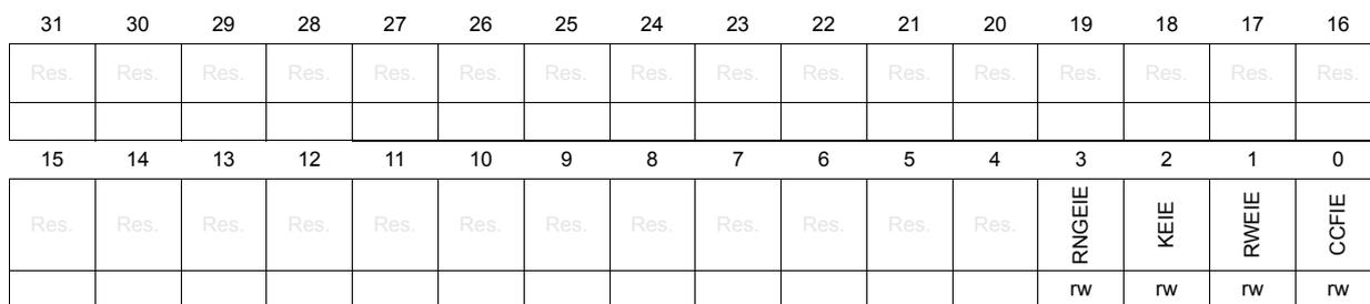
| 31 | 30 | 29 | 28 | 27 | 26 | 25 | 24 | 23 | 22 | 21 | 20 | 19 | 18 | 17 | 16 |
| Res. | Res. | Res. | Res. | Res. | Res. | Res. | Res. | Res. | Res. | Res. | Res. | Res. | Res. | Res. | Res. |
| 15 | 14 | 13 | 12 | 11 | 10 | 9 | 8 | 7 | 6 | 5 | 4 | 3 | 2 | 1 | 0 |
| Res. | Res. | Res. | Res. | Res. | Res. | Res. | Res. | Res. | Res. | Res. | Res. | RNGEIE | KEIE | RWEIE | CCFIE |
| rw | rw | rw | rw |
Bits 31:4 Reserved, must be kept at reset value.
Bit 3 RNGEIE : RNG error interrupt enable
This bit enables or disables (masks) the SAES interrupt generation when RNGEIF (RNG error flag) is set.
0: Disabled (masked)
1: Enabled (not masked)
Bit 2 KEIE : Key error interrupt enable
This bit enables or disables (masks) the SAES interrupt generation when KEIF (key error flag) is set.
0: Disabled (masked)
1: Enabled (not masked)
Bit 1 RWEIE : Read or write error interrupt enable
This bit enables or disables (masks) the SAES interrupt generation when RWEIF (read and/or write error flag) is set.
0: Disabled (masked)
1: Enabled (not masked)
Bit 0 CCFIE : Computation complete flag interrupt enable
This bit enables or disables (masks) the SAES interrupt generation when CCF (computation complete flag) is set.
0: Disabled (masked)
1: Enabled (not masked)
50.7.18 SAES interrupt status register (SAES_ISR)
Address offset: 0x304
Reset value: 0x0000 0000
| 31 | 30 | 29 | 28 | 27 | 26 | 25 | 24 | 23 | 22 | 21 | 20 | 19 | 18 | 17 | 16 |
|---|---|---|---|---|---|---|---|---|---|---|---|---|---|---|---|
| Res. | Res. | Res. | Res. | Res. | Res. | Res. | Res. | Res. | Res. | Res. | Res. | Res. | Res. | Res. | Res. |
| 15 | 14 | 13 | 12 | 11 | 10 | 9 | 8 | 7 | 6 | 5 | 4 | 3 | 2 | 1 | 0 |
| Res. | Res. | Res. | Res. | Res. | Res. | Res. | Res. | Res. | Res. | Res. | Res. | RNGEIF | KEIF | RWEIF | CCF |
| r | r | r | r |
Bits 31:4 Reserved, must be kept at reset value.
Bit 3 RNGEIF : RNG error interrupt flag
This read-only bit is set by hardware when an error is detected on RNG bus interface (e.g. bad entropy).
0: RNG bus is functional
1: Error detected on RNG bus interface (random seed fetching error)
RNGEIF bit is cleared when application sets the corresponding bit of SAES_ICR register. An interrupt is generated if the RNGEIF bit has been previously set in the SAES_IER register. Clearing this bit triggers the reload of a new random number from RNG peripheral.
Bit 2 KEIF : Key error interrupt flag
This read-only bit is set by hardware when key information failed to load into key registers or key register usage is forbidden.
0: No key error detected
1: Key information failed to load into key registers, or key register use is forbidden
Setting the corresponding bit of the SAES_ICR register clears the KEIF and generates interrupt if the KEIE bit of the SAES_IER register is set.
KEIF is triggered upon any of the following errors:
–SAES fails to load the DHUK (KEYSEL = 001 or 100).
–SAES fails to load the BHK (KEYSEL = 010 or 100) respecting the correct order.
–AES fails to load the key shared by SAES peripheral (KMOD = 10).
– When KEYVALID = 1 and (KEYPROT = 1 or KEYSEL is not 0x0), the security context of the application that loads the key (secure or nonsecure) does not match the security attribute of the access to SAES_CR or SAES_DOUT. In this case, KEYVALID and EN bits are cleared.
–SAES_KEYRx register write does not respect the correct order. (For KEYSIZE = 0, SAES_KEYR0 then SAES_KEYR1 then SAES_KEYR2 then SAES_KEYR3 register, or reverse. For KEYSIZE = 1, SAES_KEYR0 then SAES_KEYR1 then SAES_KEYR2 then SAES_KEYR3 then SAES_KEYR4 then SAES_KEYR5 then SAES_KEYR6 then SAES_KEYR7, or reverse).
KEIF must be cleared by the application software, otherwise KEYVALID cannot be set.
Bit 1 RWEIF : Read or write error interrupt flag
This read-only bit is set by hardware when a RDERR or a WRERR error flag is set in the SAES_SR register.
0: No read or write error detected
1: Read or write error detected (see SAES_SR register for details)
RWEIF bit is cleared when application sets the corresponding bit of SAES_ICR register. An interrupt is generated if the RWEIE bit has been previously set in the SAES_IER register.
This flag has no meaning when key derivation mode is selected.
Bit 0 CCF : Computation complete flag
This flag indicates whether the computation is completed:
0: Not completed
1: Completed
The flag is set by hardware upon the completion of the computation. It is cleared by software, upon setting the CCF bit of the SAES_ISR register.
Upon the flag setting, an interrupt is generated if enabled through the CCFIE bit of the SAES_IER register.
The flag is significant only when the DMAOUTEN bit is 0. It may stay high when DMA_EN is 1.
50.7.19 SAES interrupt clear register (SAES_ICR)
Address offset: 0x308
Reset value: 0x0000 0000
| 31 | 30 | 29 | 28 | 27 | 26 | 25 | 24 | 23 | 22 | 21 | 20 | 19 | 18 | 17 | 16 |
|---|---|---|---|---|---|---|---|---|---|---|---|---|---|---|---|
| Res. | Res. | Res. | Res. | Res. | Res. | Res. | Res. | Res. | Res. | Res. | Res. | Res. | Res. | Res. | Res. |
| 15 | 14 | 13 | 12 | 11 | 10 | 9 | 8 | 7 | 6 | 5 | 4 | 3 | 2 | 1 | 0 |
| Res. | Res. | Res. | Res. | Res. | Res. | Res. | Res. | Res. | Res. | Res. | Res. | RNGEIF w | KEIF w | RWEIF w | CCF w |
Bits 31:4 Reserved, must be kept at reset value.
Bit 3 RNGEIF : RNG error interrupt flag clear
Application must set this bit to clear the RNGEIF status bit in SAES_ISR register.
Bit 2 KEIF : Key error interrupt flag clear
Setting this bit clears the KEIF status bit of the SAES_ISR register.
Bit 1 RWEIF : Read or write error interrupt flag clear
Setting this bit clears the RWEIF status bit of the SAES_ISR register, and both RDERR and WRERR flags in the SAES_SR register.
Bit 0 CCF : Computation complete flag clear
Setting this bit clears the CCF status bit of the SAES_SR and SAES_ISR registers.
50.7.20 SAES register map
Table 483. SAES register map and reset values
| Offset | Register | 31 | 30 | 29 | 28 | 27 | 26 | 25 | 24 | 23 | 22 | 21 | 20 | 19 | 18 | 17 | 16 | 15 | 14 | 13 | 12 | 11 | 10 | 9 | 8 | 7 | 6 | 5 | 4 | 3 | 2 | 1 | 0 |
|---|---|---|---|---|---|---|---|---|---|---|---|---|---|---|---|---|---|---|---|---|---|---|---|---|---|---|---|---|---|---|---|---|---|
| 0x000 | SAES_CR | IPRST | KEYSEL[2:0] | KSHARED[1:0] | KMOD[1:0] | Res. | KEYPROT | KEYSIZE | Res. | CHMOD[2] | Res. | Res. | DMAOUTEN | DMAINEN | Res. | Res. | Res. | Res. | Res. | CHMOD[1:0] | MODE[1:0] | DATATYPE[1:0] | EN | ||||||||||
| Reset value | 0 | 0 | 0 | 0 | 0 | 0 | 0 | 0 | 0 | 0 | 0 | 0 | 0 | 0 | 0 | 0 | 0 | 0 | 0 | 0 | |||||||||||||
| 0x004 | SAES_SR | Res. | Res. | Res. | Res. | Res. | Res. | Res. | Res. | Res. | Res. | Res. | Res. | Res. | Res. | Res. | Res. | Res. | Res. | Res. | Res. | Res. | Res. | Res. | Res. | KEYVALID | Res. | Res. | Res. | BUSY | WRERR | RDERR | CCF |
| Reset value | 0 | 0 | 0 | 0 | 0 | ||||||||||||||||||||||||||||
| 0x008 | SAES_DINR | DIN[31:0] | |||||||||||||||||||||||||||||||
| Reset value | 0 | 0 | 0 | 0 | 0 | 0 | 0 | 0 | 0 | 0 | 0 | 0 | 0 | 0 | 0 | 0 | 0 | 0 | 0 | 0 | 0 | 0 | 0 | 0 | 0 | 0 | 0 | 0 | 0 | 0 | 0 | 0 | |
| 0x00C | SAES_DOUTR | DOUT[31:0] | |||||||||||||||||||||||||||||||
| Reset value | 0 | 0 | 0 | 0 | 0 | 0 | 0 | 0 | 0 | 0 | 0 | 0 | 0 | 0 | 0 | 0 | 0 | 0 | 0 | 0 | 0 | 0 | 0 | 0 | 0 | 0 | 0 | 0 | 0 | 0 | 0 | 0 | |
| 0x010 | SAES_KEYR0 | KEY[31:0] | |||||||||||||||||||||||||||||||
| Reset value | 0 | 0 | 0 | 0 | 0 | 0 | 0 | 0 | 0 | 0 | 0 | 0 | 0 | 0 | 0 | 0 | 0 | 0 | 0 | 0 | 0 | 0 | 0 | 0 | 0 | 0 | 0 | 0 | 0 | 0 | 0 | 0 | |
| 0x014 | SAES_KEYR1 | KEY[63:32] | |||||||||||||||||||||||||||||||
| Reset value | 0 | 0 | 0 | 0 | 0 | 0 | 0 | 0 | 0 | 0 | 0 | 0 | 0 | 0 | 0 | 0 | 0 | 0 | 0 | 0 | 0 | 0 | 0 | 0 | 0 | 0 | 0 | 0 | 0 | 0 | 0 | 0 | |
| 0x018 | SAES_KEYR2 | KEY[95:64] | |||||||||||||||||||||||||||||||
| Reset value | 0 | 0 | 0 | 0 | 0 | 0 | 0 | 0 | 0 | 0 | 0 | 0 | 0 | 0 | 0 | 0 | 0 | 0 | 0 | 0 | 0 | 0 | 0 | 0 | 0 | 0 | 0 | 0 | 0 | 0 | 0 | 0 | |
| 0x01C | SAES_KEYR3 | KEY[127:96] | |||||||||||||||||||||||||||||||
| Reset value | 0 | 0 | 0 | 0 | 0 | 0 | 0 | 0 | 0 | 0 | 0 | 0 | 0 | 0 | 0 | 0 | 0 | 0 | 0 | 0 | 0 | 0 | 0 | 0 | 0 | 0 | 0 | 0 | 0 | 0 | 0 | 0 | |
| 0x020 | SAES_IVR0 | IVI[31:0] | |||||||||||||||||||||||||||||||
| Reset value | 0 | 0 | 0 | 0 | 0 | 0 | 0 | 0 | 0 | 0 | 0 | 0 | 0 | 0 | 0 | 0 | 0 | 0 | 0 | 0 | 0 | 0 | 0 | 0 | 0 | 0 | 0 | 0 | 0 | 0 | 0 | 0 | |
| 0x024 | SAES_IVR1 | IVI[63:32] | |||||||||||||||||||||||||||||||
| Reset value | 0 | 0 | 0 | 0 | 0 | 0 | 0 | 0 | 0 | 0 | 0 | 0 | 0 | 0 | 0 | 0 | 0 | 0 | 0 | 0 | 0 | 0 | 0 | 0 | 0 | 0 | 0 | 0 | 0 | 0 | 0 | 0 | |
| 0x028 | SAES_IVR2 | IVI[95:64] | |||||||||||||||||||||||||||||||
| Reset value | 0 | 0 | 0 | 0 | 0 | 0 | 0 | 0 | 0 | 0 | 0 | 0 | 0 | 0 | 0 | 0 | 0 | 0 | 0 | 0 | 0 | 0 | 0 | 0 | 0 | 0 | 0 | 0 | 0 | 0 | 0 | 0 | |
| 0x02C | SAES_IVR3 | IVI[127:96] | |||||||||||||||||||||||||||||||
| Reset value | 0 | 0 | 0 | 0 | 0 | 0 | 0 | 0 | 0 | 0 | 0 | 0 | 0 | 0 | 0 | 0 | 0 | 0 | 0 | 0 | 0 | 0 | 0 | 0 | 0 | 0 | 0 | 0 | 0 | 0 | 0 | 0 | |
| 0x030 | SAES_KEYR4 | KEY[159:128] | |||||||||||||||||||||||||||||||
| Reset value | 0 | 0 | 0 | 0 | 0 | 0 | 0 | 0 | 0 | 0 | 0 | 0 | 0 | 0 | 0 | 0 | 0 | 0 | 0 | 0 | 0 | 0 | 0 | 0 | 0 | 0 | 0 | 0 | 0 | 0 | 0 | 0 | |
| 0x034 | SAES_KEYR5 | KEY[191:160] | |||||||||||||||||||||||||||||||
| Reset value | 0 | 0 | 0 | 0 | 0 | 0 | 0 | 0 | 0 | 0 | 0 | 0 | 0 | 0 | 0 | 0 | 0 | 0 | 0 | 0 | 0 | 0 | 0 | 0 | 0 | 0 | 0 | 0 | 0 | 0 | 0 | 0 | |
| 0x038 | SAES_KEYR6 | KEY[223:192] | |||||||||||||||||||||||||||||||
| Reset value | 0 | 0 | 0 | 0 | 0 | 0 | 0 | 0 | 0 | 0 | 0 | 0 | 0 | 0 | 0 | 0 | 0 | 0 | 0 | 0 | 0 | 0 | 0 | 0 | 0 | 0 | 0 | 0 | 0 | 0 | 0 | 0 | |
| 0x03C | SAES_KEYR7 | KEY[255:224] | |||||||||||||||||||||||||||||||
| Reset value | 0 | 0 | 0 | 0 | 0 | 0 | 0 | 0 | 0 | 0 | 0 | 0 | 0 | 0 | 0 | 0 | 0 | 0 | 0 | 0 | 0 | 0 | 0 | 0 | 0 | 0 | 0 | 0 | 0 | 0 | 0 | 0 | |
| 0x040-0x2FF | Reserved | Res. | Res. | Res. | Res. | Res. | Res. | Res. | Res. | Res. | Res. | Res. | Res. | Res. | Res. | Res. | Res. | Res. | Res. | Res. | Res. | Res. | Res. | Res. | Res. | Res. | Res. | Res. | Res. | Res. | Res. | Res. | Res. |
Table 483. SAES register map and reset values (continued)
| Offset | Register | 31 | 30 | 29 | 28 | 27 | 26 | 25 | 24 | 23 | 22 | 21 | 20 | 19 | 18 | 17 | 16 | 15 | 14 | 13 | 12 | 11 | 10 | 9 | 8 | 7 | 6 | 5 | 4 | 3 | 2 | 1 | 0 | |
|---|---|---|---|---|---|---|---|---|---|---|---|---|---|---|---|---|---|---|---|---|---|---|---|---|---|---|---|---|---|---|---|---|---|---|
| 0x300 | SAES_IER | Res. | Res. | Res. | Res. | Res. | Res. | Res. | Res. | Res. | Res. | Res. | Res. | Res. | Res. | Res. | Res. | Res. | Res. | Res. | Res. | Res. | Res. | Res. | Res. | Res. | Res. | Res. | Res. | Res. | RNGEIE | KEIE | RWEIE | CCFIE |
| Reset value | 0 | 0 | 0 | 0 | ||||||||||||||||||||||||||||||
| 0x304 | SAES_ISR | Res. | Res. | Res. | Res. | Res. | Res. | Res. | Res. | Res. | Res. | Res. | Res. | Res. | Res. | Res. | Res. | Res. | Res. | Res. | Res. | Res. | Res. | Res. | Res. | Res. | Res. | Res. | Res. | Res. | RNGEIF | KEIF | RWEIF | CCF |
| Reset value | 0 | 0 | 0 | 0 | ||||||||||||||||||||||||||||||
| 0x308 | SAES_ICR | Res. | Res. | Res. | Res. | Res. | Res. | Res. | Res. | Res. | Res. | Res. | Res. | Res. | Res. | Res. | Res. | Res. | Res. | Res. | Res. | Res. | Res. | Res. | Res. | Res. | Res. | Res. | Res. | Res. | RNGEIF | KEIF | RWEIF | CCF |
| Reset value | 0 | 0 | 0 | 0 |
Refer to Section 2.3 on page 140 for the register boundary addresses.