44. DSI Host (DSI)
This section applies to STM32U599/5A9/5F9/5G9 devices only.
44.1 DSI introduction
Portions Copyright (c) Synopsys, Inc. All rights reserved. Used with permission.
The display serial interface (DSI) is part of a group of communication protocols defined by the MIPI ® Alliance.
The MIPI ® DSI Host controller is a digital core that implements all protocol functions defined in the MIPI ® DSI specification. It provides an interface between the system and the MIPI ® D-PHY, allowing the user to communicate with a DSI-compliant display.
44.2 Standard and references
- • MIPI
®
Alliance Specification for Display Serial interface (DSI)
v1.1 - 22 November 2011 - • MIPI
®
Alliance Specification for Display Bus interface (DBI-2)
v2.00 - 16 November 2005 - • MIPI
®
Alliance Specification for Display Command set (DCS)
v1.1 - 22 November 2011 - • MIPI
®
Alliance Specification for Display Pixel interface (DPI-2)
v2.00 - 15 September 2005 - • MIPI
®
Alliance Specification for Stereoscopic Display Formats (SDF)
v1.0 - 22 November 2011 - • MIPI
®
Alliance Specification for D-PHY
v1.1 - 7 November 2011
44.3 DSI Host main features
- • Compliant with MIPI ® Alliance standards (see Section 44.2 )
- • Interface with MIPI ® D-PHY
- • Supports all commands defined in the MIPI
®
Alliance specification for DCS:
- – Transmission of all command mode packets through the APB interface
- – Transmission of commands in low-power and high-speed during video mode
- • Supports up to two D-PHY data lanes
- • Bidirectional communication and escape mode support through Data lane 0
- • Supports non continuous clock in D-PHY clock lane for additional power saving
- • Supports ultra low-power mode with PLL disabled
- • ECC and checksum capabilities
- • Support for end of transmission packet (EoTp)
- • Fault recovery schemes
- • Configurable selection of system interfaces:
- – AMBA APB for control and optional support for generic and DCS commands
- – Video mode interface through LTDC
- – Adapted command mode interface through LTDC
- – Independently programmable virtual channel ID in video mode, adapted command mode, and APB register interface
- • Video mode interfaces features:
- – LTDC interface color coding mappings into 24-bit interface:
- • 16-bit RGB, configurations 1, 2, and 3
- • 18-bit RGB, configurations 1 and 2
- • 24-bit RGB
- – Extended resolutions beyond the DPI standard maximum resolution of 800x480 pixels
- – Maximum resolution is limited by available DSI physical link bandwidth:
- • Number of lanes: 2
- • Maximum speed per lane: 500 Mbit/s
- • See examples in Section 44.4.3
- – LTDC interface color coding mappings into 24-bit interface:
- • Adapted interface features:
- – Support for sending large amounts of data through the memory_write_start (WMS) and memory_write_continue (WMC) DCS commands
- – LTDC interface color coding mappings into 24-bit interface:
- • 16-bit RGB, configurations 1, 2, and 3
- • 18-bit RGB, configurations 1 and 2
- • 24-bit RGB
- • Video mode pattern generator:
- – Vertical and horizontal color bar generation without LTDC stimuli
- – BER pattern without LTDC stimuli
44.4 DSI Host functional description
44.4.1 General description
The MIPI® DSI Host includes dedicated video interfaces internally connected to the LTDC and a generic APB interface that can be used to transmit information to the display. More in detail:
- • LTDC interface:
- – Used to transmit information in video mode, in which the transfers from the host processor to the peripheral take the form of a real-time pixel stream (DPI).
- – Through a customized mode, this interface can be used to transmit information in full bandwidth in the adapted command mode (DBI).
- • APB register interface: allows the transmission of generic information in command mode, and follows a proprietary register interface. This interface can operate concurrently with either LTDC interface in either video mode or adapted command mode.
- • Video mode pattern generator: allows the transmission of horizontal/vertical color bar and D-PHY BER testing pattern without any kind of stimuli.
The block diagram is shown in Figure 412 .
Figure 412. DSI block diagram
44.4.2 DSI Host pins and internal signals
Table 434 and Table 435 list, respectively, the DSI pins (alternate functions) and the internal input/output signals.
Table 434. DSI pins
| Signal name | Signal type | Description |
|---|---|---|
| DSI_D0P/D0N | Input/Output | Differential Data lane 0 |
| DSI_D1P/D1N | Output | Differential Data lane 1 |
| Signal name | Signal type | Description |
|---|---|---|
| DSI_CKP/CKN | Output | Differential clock |
| DSI_TE | Input | DSI tearing effect pin |
| Signal name | Signal type | Description |
|---|---|---|
| dsi_it | Output | DSI global interrupt |
44.4.3 Supported resolutions and frame rates
The DSI specification does not define supported standard resolutions or frame rates. Display resolution, blanking periods, synchronization events duration, frame rates, and pixel color depth play a fundamental role in the required bandwidth. In addition, other link-related attributes can influence the ability of the link to support a DSI-specific device, namely display input buffering capabilities, video transmission mode (burst or non-burst), bus turn-around (BTA) time, concurrent command mode traffic in a video mode transmission, or display device specifics. All these variables make it difficult to define a standard procedure to estimate the minimum lane rate and the minimum number of lanes that support a specific display device.
The basic assumptions for estimates are:
- • clock lane frequency is 250 MHz, resulting in a bandwidth of 500 Mbit/s for each data lane
- • the display must be capable of buffering the pixel data at the speed at which it is delivered in the DSI link
- • no significant control traffic is present on the link when the pixel data are transmitted.
44.4.4 System level architecture
Figure 413 shows the architecture of the DSI Host.
Figure 413. DSI Host architecture
The diagram illustrates the DSI Host architecture. On the left, an LTDC block is connected to a DSI Wrapper via Ctrl, RGB, and APB signals. The DSI Wrapper is connected to the DSI Host block via RGB and APB signals. The DSI Host block contains several sub-components: LTDC I/F, APB to Generic, Register bank, Packet handler, D-PHY I/F, and Error management. The DSI Host is connected to a D-PHY block via PPI signals. The D-PHY block is connected to external pins: DATAP1, DATAN1, DATAP0, DATAN0, CLKP, and CLKN. Above the D-PHY block, Bias and PLL blocks are shown, with connections from the DSI Host to them.
The different parts have the following functions:
- • The DSI Wrapper ensures the interfacing between the LTDC and the DSI Host kernel. It can adapt the color mode, and manages the tearing effect (TE) for automatic frame buffer update in adapted command mode. The DSI Wrapper also controls the DSI bias, the DSI PLL and specific functions of the MIPI® D-PHY.
- • The LTDC interface captures the data and control signals from the LTDC and conveys them to a FIFO for video control signals and another one for the pixel data. This data is then used to build one of the following:
- – Video packets, when in video mode (see Section 44.5 )
- – The memory_write_start and memory_write_continue DCS commands, when in adapted command mode (see Section 44.6 )
- • The register bank is accessible through a standard APB interface, providing access to the DSI Host registers for configuration and control. There is also a fully programmable interrupt generator to inform the system about certain events.
- • The PHY interface control is responsible for managing the D-PHY interface. It acknowledges the current operation and enables low-power transmission/reception or a high-speed transmission. It also performs data splitting between available D-PHY lanes for high-speed transmission.
- • The packet handler schedules the activities inside the link. It performs several functions based on the currently operational interfaces and the used video transmission mode (burst mode or non-burst mode with sync pulses or sync events). It builds long or short packets generating correspondent ECC and CRC codes. This block also performs the following functions:
- – packet reception
- – validation of packet header by checking the ECC
- – header correction and notification for single-bit errors
- – termination of reception
- – multiple header error notification
- – depending on the virtual channel of the incoming packet, the handler routes the output data to the respective port.
- • The APB-to-generic block bridges the APB operations into FIFOs holding the generic commands. The block interfaces with the following FIFOs:
- – Command FIFO
- – Write payload FIFO
- – Read payload FIFO
- • The error management notifies and monitors the error conditions on the DSI link. It controls the timers used to determine if a timeout condition occurred, performing an internal soft reset and triggering an interruption notification.
44.5 Functional description: video mode on LTDC interface
The LTDC interface captures the data and control signals and conveys them to the FIFO interfaces that transmit them to the DSI link.
Two different streams of data are present at the interface, namely video control signals and pixel data. Depending on the interface color coding, the pixel data is disposed differently throughout the LTDC bus.
Interface pixel color coding is summarized in Table 436 .
Table 436. Location of color components in the LTDC interface
| Location | 16-bit | 18-bit | 24-bit | |||
|---|---|---|---|---|---|---|
| Config 1 | Config 2 | Config 3 | Config 1 | Config 2 | ||
| D23 | - | - | - | - | - | R[7] |
| D22 | - | - | - | - | - | R[6] |
| D21 | - | - | R[4] | - | R[5] | R[5] |
| D20 | - | R[4] | R[3] | - | R[4] | R[4] |
| D19 | - | R[3] | R[2] | - | R[3] | R[3] |
| D18 | - | R[2] | R[1] | - | R[2] | R[2] |
| D17 | - | R[1] | R[0] | R[5] | R[1] | R[1] |
| D16 | - | R[0] | - | R[4] | R[0] | R[0] |
| D15 | R[4] | - | - | R[3] | - | G[7] |
| D14 | R[3] | - | - | R[2] | - | G[6] |
| D13 | R[2] | G[5] | G[5] | R[1] | G[5] | G[5] |
| D12 | R[1] | G[4] | G[4] | R[0] | G[4] | G[4] |
| D11 | R[0] | G[3] | G[3] | G[5] | G[3] | G[3] |
| D10 | G[5] | G[2] | G[2] | G[4] | G[2] | G[2] |
| D9 | G[4] | G[1] | G[1] | G[3] | G[1] | G[1] |
| D8 | G[3] | G[0] | G[0] | G[2] | G[0] | G[0] |
| D7 | G[2] | - | - | G[1] | - | B[7] |
| D6 | G[1] | - | - | G[0] | - | B[6] |
| D5 | G[0] | - | B[4] | B[5] | B[5] | B[5] |
| D4 | B[4] | B[4] | B[3] | B[4] | B[4] | B[4] |
| D3 | B[3] | B[3] | B[2] | B[3] | B[3] | B[3] |
| D2 | B[2] | B[2] | B[1] | B[2] | B[2] | B[2] |
| D1 | B[1] | B[1] | B[0] | B[1] | B[1] | B[1] |
| D0 | B[0] | B[0] | - | B[0] | B[0] | B[0] |
The LTDC interface can be configured to increase flexibility and promote its correct use for several systems. The following configuration options are available:
- • Polarity control: all the control signals are programmable to change the polarity depending on the LTDC configuration. It is recommended to keep the default polarity configuration in both LTDC, DSI Host and DSI Wrapper, to guarantee a correct behavior.
- • After the core reset, DSI Host waits for the first VSYNC active transition to start signal sampling, including pixel data, thus avoiding starting the transmission of the image data in the middle of a frame.
- • If interface pixel color coding is 18 bits and the 18-bit loosely packed stream is disabled, the number of pixels programmed in the VPSIZE field must be a multiple of four. This means that in this mode, the two LSBs in the configuration are always inferred as zero. The specification states that in this mode, the pixel line size must be a multiple of four.
- • To avoid FIFO underflows and overflows, the configured number of pixels is assumed to be received from the LTDC at all times.
- • To keep the memory organized with respect to the packet scheduling, the number of pixels per packet parameter is used to separate the memory space of different video packets.
For SHTDN and COLM sampling and transmission, the video streaming from the LTDC must be active. This means that if the LTDC is not actively generating the video signals like VSYNC and HSYNC, these signals are not transmitted through the DSI link. Because of such constraints and for commands to be correctly transmitted, the first VSYNC active pulse must occur for the command sampling and transmission. When shutting down the display, it is necessary for the LTDC to be kept active for one frame after the command being issued. This ensures that the commands are correctly transmitted before actually disabling the video generation at the LTDC interface.
The SHTDN and COLM values can be programmed in the DSI Wrapper control register (DSI_WCR).
For all of the data types, one entire pixel is received per each clock cycle. The number of pixels of payload is restricted to a multiple of a value, as shown in Table 437 .
Table 437. Multiplicity of the payload size in pixels for each data type
| Value | Data types |
|---|---|
| 1 | 16-bit 18-bit loosely packed 24-bit |
| 2 | Loosely packed pixel stream |
| 4 | 18-bit non-loosely packed |
44.5.1 Video transmission mode
There are different video transmission modes, namely:
- • Burst mode
- • Non-burst mode
- – Non-burst mode with sync pulse
- – Non-burst mode with sync event
Burst mode
In this mode, the entire active pixel line is buffered into a FIFO and transmitted in a single packet with no interruptions. This transmission mode requires that the DPI pixel FIFO has the capacity to store a full line of active pixel data inside it. This mode is optimally used when the difference between the pixel required bandwidth and DSI link bandwidth is significant, it enables the DSI Host to quickly dispatch the entire active video line in a single burst of data and then return to low-power mode.
Non-burst mode
In this mode, the processor uses the partitioning properties of the DSI Host to divide the video line transmission into several DSI packets. This is done to match the pixel required bandwidth with the DSI link bandwidth. With this mode, the controller configuration does not require a full line of pixel data to be stored inside the LTDC interface pixel FIFO. It requires only the content of one video packet.
Guidelines for selecting the burst or non-burst mode
Selecting the burst and non-burst mode is mainly dependent on the system configuration and the device requirements. Choose the video transmission mode that suits the application scenario. The burst mode is more beneficial because it increases the probability of the link spending more time in the low-power mode, decreasing power consumption. The following conditions must be met to get the maximum benefits from the burst mode of operation:
- • The DSI Host core must have sufficient pixel memory to store an entire pixel line to avoid the overflow of the internal FIFOs.
- • The display device must support receiving a full pixel line in a single packet burst to avoid the overflow on the reception buffer.
- • The DSI output bandwidth must be higher than the LTDC interface input bandwidth in a relation that enables the link to go to low-power once per line.
If the system cannot meet these requirements, it is likely that the pixel data is lost causing the malfunctioning of the display device while using the burst mode. These errors are related to the capabilities of the system to store the temporary pixel data.
If all the conditions for using the burst mode cannot be met, use the non-burst mode to avoid errors. The non-burst mode provides a better matching of rates for pixel transmission, enabling:
- • only a certain number of pixels to be stored in the memory, and not requiring a full pixel line (lesser LTDC interface RAM requirements in the DSI Host)
- • operation with devices that support only a small amount of pixel buffering (less than a full pixel line).
The DSI non-burst mode must be configured so that the DSI output pixel ratio matches with the LTDC interface input pixel ratio, reducing the memory requirements on both host and/or
device side. This is achieved by dividing a pixel line into several chunks of pixels and optionally interleaving them with null packets.
The following equations show how the DSI Host core transmission parameters must be programmed in non-burst mode to match the DSI link pixel output ratio (left hand side of the “=” sign) and LTDC interface pixel input (right hand side of the “=” sign).
When the null packets are enabled:
When the null packets are disabled:
44.5.2 Updating the LTDC interface configuration in video mode
It is possible to update the LTDC interface configuration on the fly without impacting the current frame. It is done with the help of shadow registers. This feature is controlled by the DSI Host video shadow control register (DSI_VSCR).
The new configuration is only used when the system requests for it. To update the video configuration during the transmission of a video frame, the configuration of that frame needs to be stored in the auxiliary registers. This way, the new frame configurations can be set through the APB interface without corrupting the current frame.
By default, this feature is disabled. To enable it, set the enable (EN) bit of the DSI Host video shadow control register (DSI_VSCR) to 1. When this feature is enabled, the system supplies the configuration stored in the auxiliary registers.
Figure 414 shows the steps needed to update the LTDC interface configuration.
Figure 414. Flow to update the LTDC interface configuration using shadow registers
graph TD
    A[Configure the LTDC interface] --> B[Request update]
    B --> C[Read DSI Host LTDC shadow control register]
    C --> D{UR}
    D -- Active --> C
    D -- Accepted --> E[Start video engine]
    E --> F[New resolution]
    F --> A
MSV35855V1
Immediate update
When the shadow register feature is active, the auxiliary registers require the LTDC configuration before the video engine starts. This means that, after a reset, update register (UR) bit is immediately granted.
When it is required to immediately update the active registers without the reset (as in Figure 415 ), ensure that the enable (EN) and update register (UR) bits of the DSI Host video shadow control register (DSI_VSCR) are set to 0.
Figure 415. Immediate update procedure

The diagram illustrates the immediate update procedure. It shows two states of the DSI Host. On the left, the DSI Host contains 'Default DPI Config', 'EN=0', and 'UR=0'. An arrow labeled 'DPI CONFIG 1' points to this state. A large yellow arrow labeled 'Video Shadow Update' points to the right state. On the right, the DSI Host contains 'DPI Config 1', 'EN=1', and 'UR=1'. A small label 'MSV35856V2' is in the bottom right corner.
Updating the configuration during the transmission of a frame using APB
To update the LTDC interface configuration, follow the steps shown in Figure 416 :
- 1. Ensure that the enable (EN) bit of the DSI Host video shadow control register (DSI_VSCR) register is set to 1.
- 2. Set the update register (UR) bit of DSI Host video shadow control register (DSI_VSCR) to 1.
- 3. Monitor the update register (UR) bit. This bit is set to 0 when the update is complete.
Figure 416. Configuration update during the transmission of a frame
The diagram illustrates the configuration update during the transmission of a frame. It shows two states of the DSI Host. On the left, the DSI Host contains 'Default DPI Config', 'EN=1', and 'UR=0'. An arrow labeled 'DPI CONFIG 1' points to this state. A large yellow arrow labeled 'Video Shadow Request' points to the right state. On the right, the DSI Host contains 'DPI Config 1', 'EN=1', and 'UR=1'. A small label 'MSV35857V2' is in the bottom right corner.
Requesting a configuration update
It is possible to request for the LTDC interface configuration update at any part of the frame. DSI Host waits until the end of the frame to change the configuration. However, avoid sending the update request during the first line of the frame because the data must propagate between clock domains.
44.6 Functional description: adapted command mode on LTDC interface
The adapted command mode, enables the system to input a stream of pixel from the LTDC that is conveyed by DSI Host using the command mode transmission (using the DCS packets). The adapted command mode also supports pixel input control rate signaling and tearing effect report mechanism.
The adapted command mode makes it possible to send large amounts of data through the memory_write_start (WMS) and memory_write_continue (WMC) DCS commands. It helps in delivering a wider data bandwidth for the memory write operations sent in command mode to MIPI® displays and to refresh large areas of pixels in high resolution displays. If additional commands such as display configuration commands, read back commands, and tearing effect initialization must be transferred, then the APB register interface must be used to complement the adapted command mode functionality.
Adapted command mode of operation supports 16 bpp, 18 bpp, and 24 bpp RGB.
To transmit the image data in adapted command mode:
- • Set command mode (CMDM) bit of the DSI Host mode configuration register (DSI_MCR) to 1.
- • Set DSI mode (DSIM) bit in the DSI Wrapper configuration register (DSI_WCFGR) to 1.
To transmit the image data, follow these steps:
- • Define the image area to be refreshed, by using the set_column_address and set_page_address DCS commands. The image area needs to be defined only once and remains effective until different values are defined.
- • Define the pixel color coding to be used by using the color coding (COLC) field in the DSI Host LTDC color coding register (DSI_LCOLCR).
- • Define the virtual channel ID of the LTDC interface generated packets using the virtual channel ID (VCID) field in the DSI Host LTDC VCID register (DSI_LVCIDR). These also need to be defined only once.
- • Start transmitting the data from the LTDC setting the LTDC enable (LTDCEN) bit of the DSI_WCR register.
Figure 417 shows the adapted command mode usage flow.
Figure 417. Adapted command mode usage flow
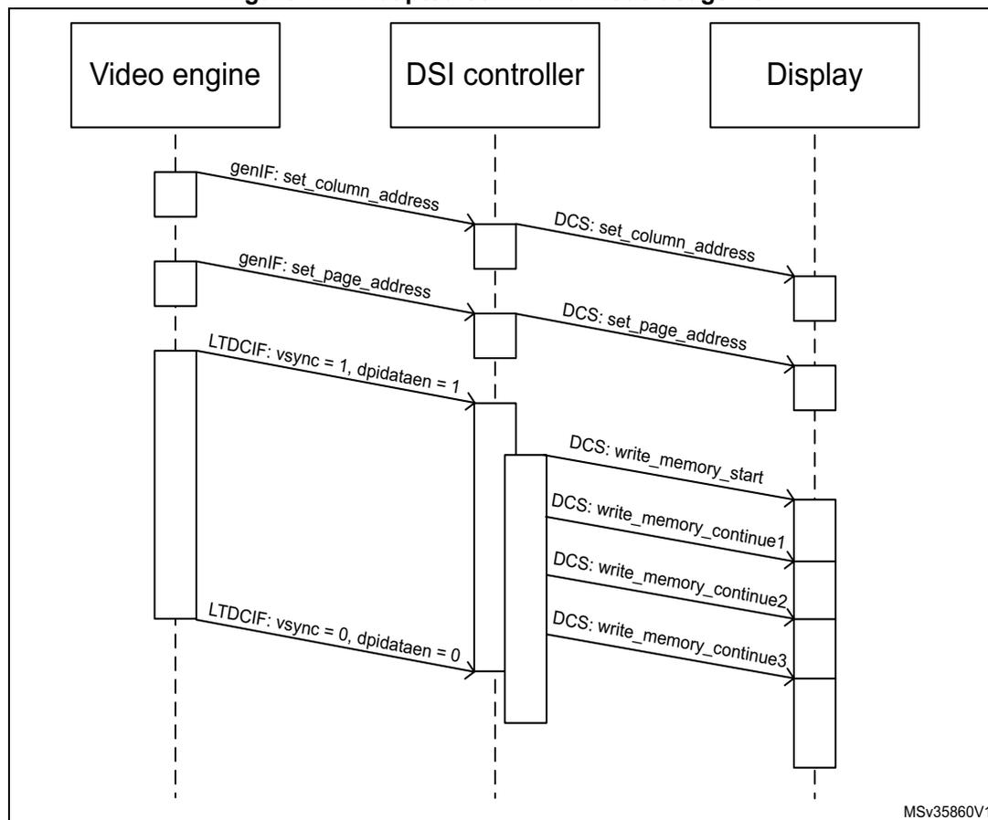
sequenceDiagram
    participant VE as Video engine
    participant DC as DSI controller
    participant D as Display
    Note left of VE:
    VE->>DC: genIF: set_column_address
    DC->>D: DCS: set_column_address
    Note left of VE:
    VE->>DC: genIF: set_page_address
    DC->>D: DCS: set_page_address
    Note left of VE:
    VE->>DC: LTDCIF: vsync = 1, dpidataen = 1
    DC->>D: DCS: write_memory_start
    Note left of VE:
    VE->>DC: LTDCIF: vsync = 0, dpidataen = 0
    DC->>D: DCS: write_memory_continue1
    DC->>D: DCS: write_memory_continue2
    DC->>D: DCS: write_memory_continue3
    Note right of D: MSv35860V1
When the command mode (CMDM) bit of the DSI Host mode configuration register (DSI_CFGR) is set to 1, the LTDC interface assumes the behavior corresponding to the adapted command mode.
In this mode, the host processor can use the LTDC interface to transmit a continuous stream of pixels to be written in the local frame buffer of the peripheral. It uses a pixel input bus to receive the pixels and controls the flow automatically to limit the stream of continuous pixels. When the first pixel is received, the current value of the command size (CMDSIZE) field of the DSI Host LTDC command configuration register (DSI_LCCR), is shadowed to the internal interface function. The interface increments a counter on every valid pixel that is input through the interface. When this pixel counter reaches command size (CMDSIZE), a command is written into the command FIFO, and the packet can be transmitted through the DSI link.
If the last pixel arrives before the counter reaches the value of shadowed command size (CMDSIZE), a WMS command is issued to the command FIFO with word count (WC) set to the number of bytes corresponding to the counter value. If more than CMDSIZE pixels are received (shadowed value), a WMS command is sent to the command FIFO with WC set to the number of bytes corresponding to the command size (CMDSIZE) and the counter is restarted.
After the first WMS command has been written to the FIFO, the circuit behaves in a similar way, but issues WMC commands instead of WMS commands. The process is repeated until the last pixel of the image is received. The core automatically starts sending a new packet
when the last pixel of the image is received, falls, or command size (CMDSIZE) limit is reached.
Synchronization with the LTDC
The DSI Wrapper performs the synchronization of the transfer process by:
- • controlling the start/halt of the LTDC
- • making the data flow control between LTDC and DSI Host.
The transfer to refresh the display frame buffer can be triggered
- • manually, setting the LTDC enable (LTDCEN) bit of the DSI Wrapper control register (DSI_WCR)
- • automatically when a tearing effect (TEIF) event occurs, and automatic refresh (AR) is enabled.
The selection between manual and automatic mode is done through the automatic refresh (AR) bit of the DSI Wrapper configuration register (DSI_WCFGR).
Once the transfer of one frame is done whatever in manual or automatic refresh mode, the DSI Wrapper halts the TFT display controller (LTDC), resetting the LTDC enable (LTDCEN) bit of the DSI Wrapper control register (DSI_WCR), and setting the end of refresh interrupt flag (ERIF) flag of the DSI Wrapper status register (DSI_WSR). If the end of refresh interrupt enable (ERIE) bit of the DSI Wrapper configuration register (DSI_WCFGR) is set, an interrupt is generated.
The end of refresh interrupt flag (ERIF) flag of the DSI Wrapper status register (DSI_WSR) can be reset setting the clear end of refresh interrupt flag (CERIF) bit of the DSI Wrapper clear interrupt flag register (DSI_WCIFR).
The halting of the TFT display controller (LTDC) by the DSI Wrapper is done synchronously on a rising edge or a falling edge of VSync according to the VSync polarity (VSPOL) bit of the DSI Wrapper configuration register (DSI_WCFGR). It is recommended to keep the default polarity to guarantee a correct behavior.
Support of tearing effect
The DSI specification supports tearing effect function in command mode displays. It enables the Host processor to receive timing accurate information about where the display peripheral is in the process of reading the content of its frame buffer.
The tearing effect can be managed through:
- • a separate pin, which is not covered in the DSI specification
- • the DSI tearing effect functionality: a set_tear_on DCS command must be issued through the APB interface using the generic interface registers.
Tearing effect through a GPIO
When the tearing effect source (TESRC) bit of the DSI Wrapper configuration register (DSI_WCFGR) is set, the tearing effect is signaled through a GPIO.
The polarity of the input signal can be configured by the tearing effect polarity (TEPOL) bit of the DSI Wrapper configuration register (DSI_WCFGR).
When the programmed edge is detected, the tearing effect interrupt flag (TEIF) bit of the DSI Wrapper interrupt and status register (DSI_WISR) is set.
If the tearing effect interrupt enable (TEIE) bit of the DSI Wrapper interrupt enable register (DSI_WIER) is set, an interrupt is generated.
Tearing effect through DSI link
When the TESRC bit of the DSI Wrapper configuration register (DSI_WCFGR) is reset, the tearing effect is managed through the DSI link:
The DSI Host performs a double bus turn-around (BTA) after sending the set_tear_on command granting the ownership of the link to the DSI display. The display holds the ownership of the bus until the tear event occurs, which is indicated to the DSI Host by a D-PHY trigger event. The DSI Host then decodes the trigger and reports the event setting the tearing effect interrupt flag (TEIF) bit of the DSI Wrapper interrupt and status register (DSI_WISR).
If the tearing effect interrupt enable (TEIE) bit of the DSI Wrapper interrupt enable register (DSI_WIER) is set, an interrupt is generated.
To use this function, it is necessary to issue a set_tear_on command after the update of the display using the WMS and WMC DCS commands. This procedure halts the DSI link until the display is ready to receive a new frame update.
The DSI Host does not automatically generate the tearing effect request (double BTA) after a WMS/WMC sequence for flexibility purposes, so several regions of the display can be updated improving DSI bandwidth usage. Tearing effect request must always be triggered by a set_tear_on command in the DSI Host implementation.
Configure the following registers to activate the tearing effect:
- • DSI Host command mode configuration register (DSI_CMCR): TEARE
- • DSI Host protocol configuration register (DSI_PCR): BTAE.
44.7 Functional description: APB register interface
The APB register interface allows the transmission of generic information in command mode, and follows a proprietary register interface. Commands sent through this interface are not constrained to comply with the DCS specification, and can include generic commands described in the DSI specification as manufacturer-specific.
The DSI Host supports the transmission of write and read command mode packets as described in the DSI specification. These packets are built using the APB register access. The DSI Host generic payload data register (DSI_GPDR) has two distinct functions based on the operation. Writing to this register sends the data as payload when sending a command mode packet. Reading this register returns the payload of a read back operation. The DSI Host generic header configuration register (DSI_GHCR) contains the command mode packet header type and header data. Writing to this register triggers the transmission of the packet implying that for a long command mode packet, the packet payload needs to be written in advance in the DSI Host generic payload data register (DSI_GPDR).
The valid packets that can be transmitted through the generic interface are the following:
- • Generic write short packet 0 parameters
- • Generic write short packet 1 parameters
- • Generic write short packet 2 parameters
- • Generic read short packet 0 parameters
- • Generic read short packet 1 parameters
- • Generic read short packet 2 parameters
- • Maximum read packet configuration
- • Generic long write packet
- • DCS write short packet 0 parameters
- • DCS write short packet 1 parameters
- • DCS read short packet 0 parameters
- • DCS write long packet.
A set of bits in the DSI Host generic packet status register (DSI_GPSR) reports the status of the FIFO associated with APB interface support.
Generic interface packets are always transported using one of the DSI transmission modes, that is, video mode or command mode. If neither of these modes is selected, the packets are not transmitted through the link, and the related FIFO eventually becomes overflowed.
44.7.1 Packet transmission using the generic interface
The transfer of packets through the APB bus is based on the following conditions:
- • The APB protocol defines that the write and read procedure takes two clock cycles each to be executed. This means that the maximum input data rate through the APB interface is always half the speed of the APB clock.
- • The data input bus has a maximum width of 32 bits. This allows for a relation to be defined between the input APB clock frequency and the maximum bit rate achievable by the APB interface.
- • The DSI link pixel bit rate when using solely APB is \( (\text{APB clock frequency}) * 16 \) Mbit/s.
- • When using only the APB interface, the theoretical DSI link maximum bit rate can be expressed as \( \text{DSI link maximum bit rate} = \text{APB clock frequency (in MHz)} * 32 / 2 \) Mbit/s.
In this formula, the number 32 represents the APB data bus width, and the division by two is present because each APB write procedure takes two clock cycles to be executed.
- • The bandwidth is dependent on the APB clock frequency; the available bandwidth increases with the clock frequency.
To drive the APB interface to achieve high bandwidth command mode traffic transported by the DSI link, the DSI Host must operate only in the command mode, and the APB interface must be the only data source in use. Thus, the APB interface has the entire bandwidth of the DSI link and does not share it with any another input interface source.
The memory write commands require the maximum throughput from the APB interface, because they contain the highest amount of data conveyed by the DSI link. While writing the packet information, first write the payload of a given packet into the payload FIFO using the DSI Host generic payload data register (DSI_GPDHR). When the payload data is for the command parameters, put the first byte to be transmitted in the least significant byte position of the APB data bus. After writing the payload, write the packet header into the command FIFO. For more information about the packet header organization on the 32-bit APB data bus, so that it is correctly stored inside the command FIFO.
When the payload data is for a memory write command, it contains pixel information and it must follow the pixel to byte conversion organization referred in the Annex A of the DCS specification.
Figures 418 to 422 show how the pixel data must be organized in the APB data write bus.
The memory write commands are conveyed in DCS long packets, encapsulated in a DSI packet. The DSI specifies that the DCS command must be present in the first payload byte of the packet. This is also included in the diagrams. In figures 418 to 422, the write memory command can be replaced by the DCS command write memory Start and write memory Continue .
Figure 418. 24 bpp APB pixel to byte organization
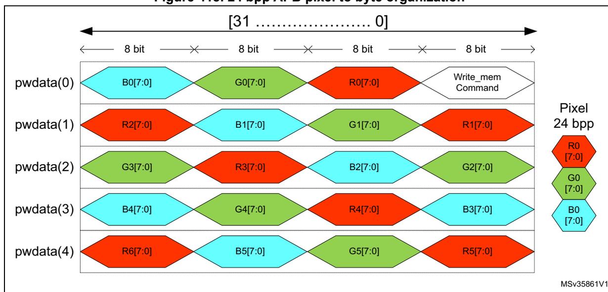
The diagram illustrates the 24 bpp APB pixel to byte organization. The APB data bus is 32 bits wide, divided into four 8-bit segments. The pixel data is organized in a 24-bit format (R0, G0, B0, R1, G1, B1, R2, G2, B2, R3, G3, B3, R4, G4, B4, R5, G5, B5). The diagram shows the mapping of these 24 bits to the 32-bit bus, with the remaining 8 bits filled with the Write_mem Command.
| APB Data Bus Segment | Pixel Data |
|---|---|
| pwdata(0) | B0[7:0], G0[7:0], R0[7:0], Write_mem Command |
| pwdata(1) | R2[7:0], B1[7:0], G1[7:0], R1[7:0] |
| pwdata(2) | G3[7:0], R3[7:0], B2[7:0], G2[7:0] |
| pwdata(3) | B4[7:0], G4[7:0], R4[7:0], B3[7:0] |
| pwdata(4) | R6[7:0], B5[7:0], G5[7:0], R5[7:0] |
Pixel 24 bpp organization:
- R0 [7:0]
- G0 [7:0]
- B0 [7:0]
MSv35861V1
Figure 419. 18 bpp APB pixel to byte organization
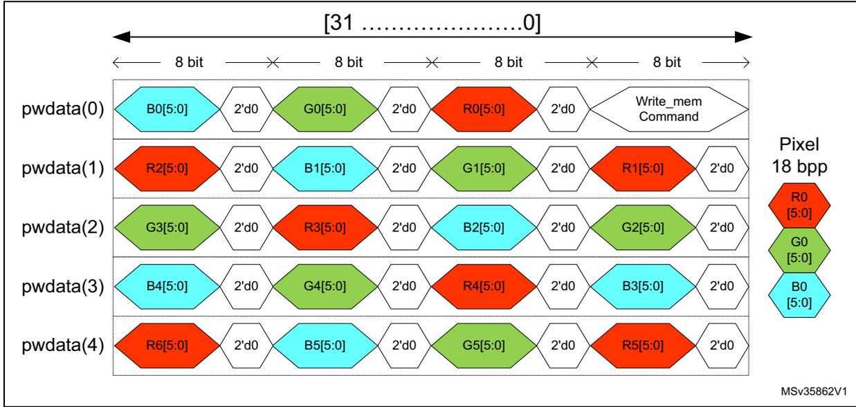
The diagram illustrates the 18 bpp APB pixel to byte organization. It shows five rows of data (pwdata(0) to pwdata(4)) and a summary of the pixel structure on the right. Each row is divided into four 8-bit segments, indicated by a double-headed arrow at the top spanning from bit 31 down to 0.
- pwdata(0): B0[5:0] (blue), 2'd0 (white), G0[5:0] (green), 2'd0 (white), R0[5:0] (red), 2'd0 (white), Write_mem Command (white), 2'd0 (white).
- pwdata(1): R2[5:0] (red), 2'd0 (white), B1[5:0] (blue), 2'd0 (white), G1[5:0] (green), 2'd0 (white), R1[5:0] (red), 2'd0 (white).
- pwdata(2): G3[5:0] (green), 2'd0 (white), R3[5:0] (red), 2'd0 (white), B2[5:0] (blue), 2'd0 (white), G2[5:0] (green), 2'd0 (white).
- pwdata(3): B4[5:0] (blue), 2'd0 (white), G4[5:0] (green), 2'd0 (white), R4[5:0] (red), 2'd0 (white), B3[5:0] (blue), 2'd0 (white).
- pwdata(4): R6[5:0] (red), 2'd0 (white), B5[5:0] (blue), 2'd0 (white), G5[5:0] (green), 2'd0 (white), R5[5:0] (red), 2'd0 (white).
On the right, a summary shows the pixel structure for 18 bpp:
- Pixel 18 bpp
- R0 [5:0] (red)
- G0 [5:0] (green)
- B0 [5:0] (blue)
MSv35862V1
Figure 420. 16 bpp APB pixel to byte organization
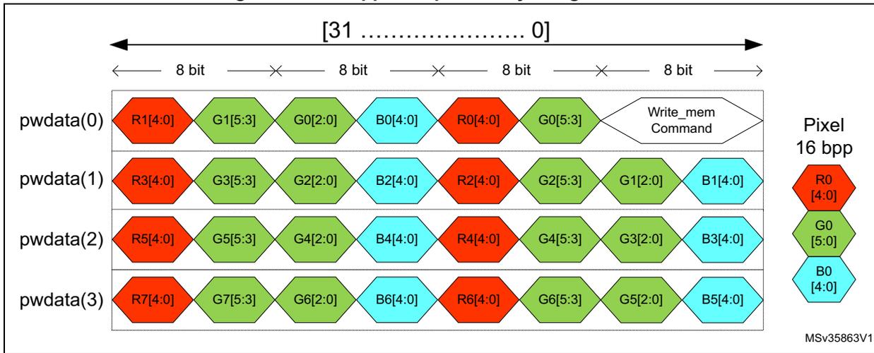
The diagram illustrates the 16 bpp APB pixel to byte organization. It shows four rows of data (pwdata(0) to pwdata(3)) and a summary of the pixel structure on the right. Each row is divided into four 8-bit segments, indicated by a double-headed arrow at the top spanning from bit 31 down to 0.
- pwdata(0): R1[4:0] (red), G1[5:3] (green), G0[2:0] (green), B0[4:0] (blue), R0[4:0] (red), G0[5:3] (green), Write_mem Command (white), 2'd0 (white).
- pwdata(1): R3[4:0] (red), G3[5:3] (green), G2[2:0] (green), B2[4:0] (blue), R2[4:0] (red), G2[5:3] (green), G1[2:0] (green), B1[4:0] (blue).
- pwdata(2): R5[4:0] (red), G5[5:3] (green), G4[2:0] (green), B4[4:0] (blue), R4[4:0] (red), G4[5:3] (green), G3[2:0] (green), B3[4:0] (blue).
- pwdata(3): R7[4:0] (red), G7[5:3] (green), G6[2:0] (green), B6[4:0] (blue), R6[4:0] (red), G6[5:3] (green), G5[2:0] (green), B5[4:0] (blue).
On the right, a summary shows the pixel structure for 16 bpp:
- Pixel 16 bpp
- R0 [4:0] (red)
- G0 [5:0] (green)
- B0 [4:0] (blue)
MSv35863V1
Figure 421. 12 bpp APB pixel to byte organization
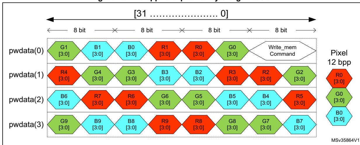
Figure 421 illustrates the 12 bpp APB pixel to byte organization. The diagram shows a 32-bit bus (bits 31 to 0) divided into four 8-bit segments. The data is organized into four rows (pwdata(0) to pwdata(3)), each containing 8 bytes. The bytes are interleaved by color (R, G, B) and bit depth (3:0). A 'Write_mem Command' is included in the first row. The resulting pixel data is 12 bpp.
| Row | Byte 0 | Byte 1 | Byte 2 | Byte 3 | Byte 4 | Byte 5 | Byte 6 | Byte 7 |
|---|---|---|---|---|---|---|---|---|
| pwdata(0) | G1 [3:0] | B1 [3:0] | B0 [3:0] | R1 [3:0] | R0 [3:0] | G0 [3:0] | Write_mem Command | |
| pwdata(1) | R4 [3:0] | G4 [3:0] | G3 [3:0] | B3 [3:0] | B2 [3:0] | R3 [3:0] | R2 [3:0] | G2 [3:0] |
| pwdata(2) | B6 [3:0] | R7 [3:0] | R6 [3:0] | G6 [3:0] | G5 [3:0] | B5 [3:0] | B4 [3:0] | R5 [3:0] |
| pwdata(3) | G9 [3:0] | B9 [3:0] | B8 [3:0] | R9 [3:0] | R8 [3:0] | G8 [3:0] | G7 [3:0] | B7 [3:0] |
Pixel 12 bpp: R0 [3:0], G0 [3:0], B0 [3:0]
MSv35864V1
Figure 422. 8 bpp APB pixel to byte organization
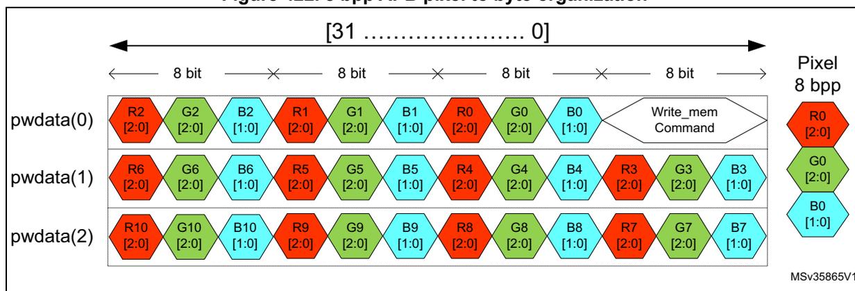
Figure 422 illustrates the 8 bpp APB pixel to byte organization. The diagram shows a 32-bit bus (bits 31 to 0) divided into four 8-bit segments. The data is organized into three rows (pwdata(0) to pwdata(2)), each containing 12 bytes. The bytes are interleaved by color (R, G, B) and bit depth (2:0 or 1:0). A 'Write_mem Command' is included in the first row. The resulting pixel data is 8 bpp.
| Row | Byte 0 | Byte 1 | Byte 2 | Byte 3 | Byte 4 | Byte 5 | Byte 6 | Byte 7 | Byte 8 | Byte 9 | Byte 10 | Byte 11 |
|---|---|---|---|---|---|---|---|---|---|---|---|---|
| pwdata(0) | R2 [2:0] | G2 [2:0] | B2 [1:0] | R1 [2:0] | G1 [2:0] | B1 [1:0] | R0 [2:0] | G0 [2:0] | B0 [1:0] | Write_mem Command | ||
| pwdata(1) | R6 [2:0] | G6 [2:0] | B6 [1:0] | R5 [2:0] | G5 [2:0] | B5 [1:0] | R4 [2:0] | G4 [2:0] | B4 [1:0] | R3 [2:0] | G3 [2:0] | B3 [1:0] |
| pwdata(2) | R10 [2:0] | G10 [2:0] | B10 [1:0] | R9 [2:0] | G9 [2:0] | B9 [1:0] | R8 [2:0] | G8 [2:0] | B8 [1:0] | R7 [2:0] | G7 [2:0] | B7 [1:0] |
Pixel 8 bpp: R0 [2:0], G0 [2:0], B0 [1:0]
MSv35865V1
44.8 Functional description: timeout counters
The DSI Host includes counters to manage timeout during the various communication phases. The duration of each timeout can be configured by the six timeout counter configuration registers (DSI_TCCR0...5).
There are two types of counters:
- • contention error detection timeout counters ( Section 44.8.1 )
- • peripheral response timeout counters ( Section 44.8.2 ).
44.8.1 Contention error detection timeout counters
The DSI Host implements a set of counters and conditions to notify the errors. It features a set of registers to control the timers used to determine if a timeout has occurred, and also contains a set of interruption status registers that are cleared upon a read operation (detailed in Table 438 ). Optionally, these registers also trigger an interrupt signal that can be used by the system to be activated when an error occurs within the DSI connection.
Table 438. Contention detection timeout counters configuration
| Timeout counter | Value register | Value field | Flag register | Flag field |
|---|---|---|---|---|
| High-speed transmission | DSI_TCCR0 | TOHSTX | DSI_ISR1 | TOHSTX |
| Low-power reception | DSI_TCCR0 | TOLPRX | DSI_ISR1 | TOLPRX |
Time units for these 16-bit counters are configured in cycles defined in the timeout clock division (TOCKDIV) field in the DSI Host clock control register (DSI_CCR).
The value written to the timeout clock division (TOCKDIV) field in the DSI Host clock control register (DSI_CCR) defines the time unit for the timeout limits using the lane byte clock as input.
This mechanism increases the range to define these limits.
High-speed transmission contention detection
The timeout duration is configured in the high-speed transmission timeout count (HSTX_TOCNT) field of the DSI Host timeout counter configuration register 1 (DSI_TCCR0). A 16-bit counter measures the time during which the high-speed mode is active.
If that counter reaches the value defined by the high-speed transmission timeout count (HSTX_TOCNT) field of the DSI Host timeout counter configuration register 1 (DSI_TCCR0), the timeout high-speed transmission (TOHSTX) bit in the DSI Host interrupt and status register 1 (DSI_ISR1) is asserted and an internal soft reset is generated to the DSI Host.
If the timeout high-speed transmission interrupt enable (TOHSTXIE) bit of the DSI Host interrupt enable register 1 (DSI_IER1) is set, an interrupt is generated.
Low-power reception contention detection
The timeout is configured in the low-power reception timeout counter (LPRX_TOCNT) field of the DSI Host timeout counter configuration register 1 (DSI_TCCR1) . A 16-bit counter measures the time during which the low-power reception is active. If that counter reaches
the value defined by the low-power reception timeout counter (LPRX_TOCNT) field of the DSI Host timeout counter configuration register 1 (DSI_TCCR1) , the timeout low-power reception (TOLPRX) bit in the DSI Host interrupt enable register 1 (DSI_IER1) is asserted and an internal soft reset is generated to the DSI Host.
If the timeout low-power reception interrupt enable (TOLPRXIE) bit of the DSI Host interrupt enable register 1 (DSI_IER1) is set, an interrupt is generated. Once the software gets notified by the interrupt, it must reset the D-PHY by deasserting and asserting the digital enable (DEN) bit of the DSI Host PHY control register (DSI_PCTLR) .
44.8.2 Peripheral response timeout counters
A peripheral may not immediately respond correctly to some received packets. For example, a peripheral receives a read request, but due to its architecture cannot access the RAM for a while (for example, the panel is being refreshed and takes some time to respond). In this case, set a timeout to ensure that the host waits long enough so that the device is able to process the previous data before receiving the new data or responding correctly to new requests.
Table 439 lists the events belonging to various categories having an associated timeout for peripheral response.
Table 439. List of events of different categories of the PRESP_TO counter
| Category | Event |
|---|---|
| Items implying a BTA PRESP_TO | Bus-turn-around |
| READ requests indicating a PRESP_TO (replicated for HS and LP) | (0x04) Generic read, no parameters short (0x14) Generic read, 1 parameter short (0x24) Generic read, 2 parameters short (0x06) DCS read, no parameters short |
| WRITE requests indicating a PRESP_TO (replicated for HS and LP) | (0x03) Generic short write, no parameters short (0x13) Generic short write, 1 parameter short (0x23) Generic short write, 2 parameters short (0x29) Generic long write long (0x05) DCS short write, no parameters short (0x15) DCS short write, 1 parameter short (0x39) DCS long write/write_LUT, command packet long (0x37) Set maximum return packet size |
The DSI Host ensures that, on sending an event that triggers a timeout, the D-PHY switches to the Stop state and a counter starts running until it reaches the value of that timeout. The link remains in the LP-11 state and unused until the timeout ends, even if there are other events ready to be transmitted.
Figures 423 to 425 illustrate the flow of counting in the PRESP_TO counter for the three categories listed in Table 439 .
Figure 423. Timing of PRESP_TO after a bus-turn-around
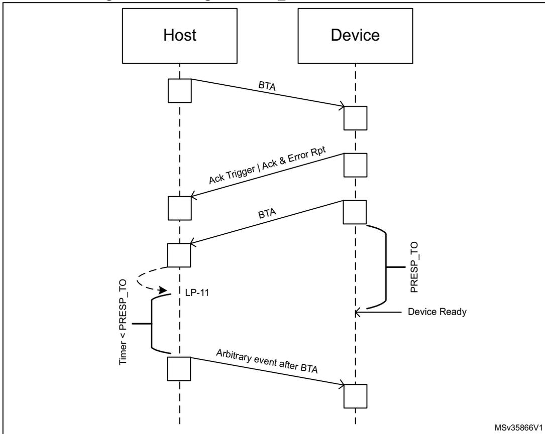
The diagram illustrates the timing of PRESP_TO after a bus-turn-around between a Host and a Device. The sequence of events is as follows:
- The Host sends a BTA (Bus Turn-Around) signal to the Device.
- The Device responds with an Ack Trigger | Ack & Error Rpt signal.
- The Host receives the response and then sends another BTA signal.
- Simultaneously, the Device enters a low-power state ( LP-11 ) and asserts the PRESP_TO signal.
- The Host's Timer < PRESP_TO is active during this period.
- An Arbitrary event after BTA occurs on the Host side.
- Finally, the Device becomes Device Ready , indicated by a signal transition.
MSV35866V1
Figure 424. Timing of PRESP_TO after a read request (HS or LP)
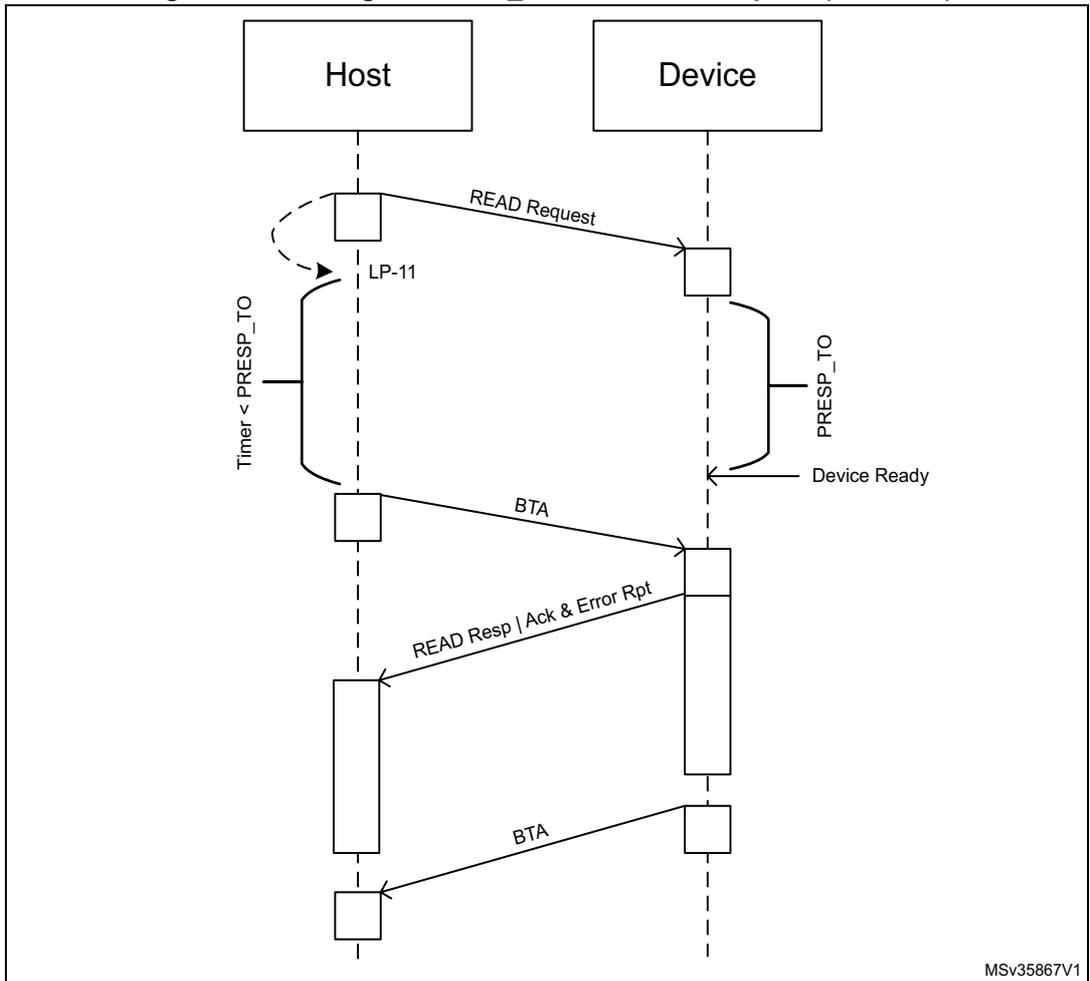
The diagram illustrates the timing sequence for a read request between a Host and a Device. The sequence of events is as follows:
- The Host sends a READ Request to the Device.
- Simultaneously, the Host enters the LP-11 state.
- A timer on the Host starts, labeled Timer < PRESP_TO .
- The Device receives the request and enters a state monitored by the PRESP_TO timer.
- When the Device is Device Ready , it initiates a BTA (Bus Turnaround) to take control of the bus.
- The Host receives the BTA and exits the LP-11 state.
- The Device then sends the READ Resp | Ack & Error Rpt to the Host.
- After the response, another BTA occurs to return bus control to the Host.
MSV35867V1
Figure 425. Timing of PRESP_TO after a write request (HS or LP)
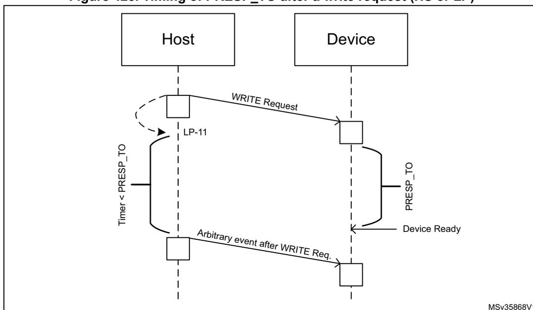
Table 440 describes the fields used for the configuration of the PRESP_TO counter.
Table 440. PRESP_TO counter configuration
| Description | Register | Field | |
|---|---|---|---|
| Period for which the DSI Host keeps the link still | After sending a High-speed read operation | DSI_TCCR1 | HSRD_TOCNT |
| After sending a Low-power read operation | DSI_TCCR2 | LPRD_TOCNT | |
| After completing a Bus-turn-around (BTA) | DSI_TCCR5 | BTA_TOCNT | |
| Period for which the DSI Host keeps the link inactive | After sending a High-speed write operation | DSI_TCCR3 | HSWR_TOCNT |
| After sending a Low-power write operation | DSI_TCCR4 | LPWR_TOCNT | |
The values in these registers are measured in number of cycles of the lane byte clock. These registers are only used in command mode because in video mode, there is a rigid timing schedule to be met to keep the display properly refreshed and it must not be broken by these or any other timeouts. Setting a given timeout to 0 disables going into LP-11 state and timeout for events of that category.
The read and the write requests in high-speed mode are distinct from those in low-power mode. For example, if HSRD_TOCNT is set to 0 and LPRD_TOCNT is set to a non-0 value, a generic read with no parameters does not activate the PRESP_TO counter in high-speed, but activates the PRESP_TO in low-power.
The DSI Host timeout counter configuration register 4 (DSI_TCCR3) includes a special Presp mode (PM) bit to change the normal behavior of PRESP_TO in Adaptive command
mode for high-speed write operation timeout. When set to 1, this bit allows the RESP_TO from HSWR_TOCNT to be used only once, when both of the following conditions are met:
- • the LTDC VSYNC signal rises and falls
- • the packets originated from the LTDC interface in adapted command mode are transmitted and its FIFO is empty again.
In this scenario, non-adapted command mode requests are not sent to the D-PHY, even if there is traffic from the generic interface ready to be sent, returning them to the Stop state. When it happens, the RESP_TO counter is activated and only when it is completed, the DSI Host sends any other traffic that is ready, as illustrated in Figure 426 .
Figure 426. Effect of prep mode at 1
![Timing diagram showing the effect of prep mode at 1 on DSI signals. The diagram illustrates the relationship between dpivsync_edpiwms, dpidataen, dpidata[29:0], edpi_fifo_empty, gen_wr_en, gen_data[31:0], link_state[1:0], link_data[31:0], and RESP_TO_active signals over time. The dpidata[29:0] signal shows data packets A10, A20, and A30 being transmitted. The gen_data[31:0] signal shows data packets B3 and X being transmitted. The link_state[1:0] signal shows a sequence of LP, HS, LP, HS, LP states. The RESP_TO_active signal is shown as a pulse during the transmission of the first data packet.](/RM0456-STM32U5/bb641e7ca4319871d023dd6044930c16_img.jpg)
The timing diagram illustrates the following signals and their states over time:
- dpivsync_edpiwms : A signal that goes high during the transmission of the first data packet (A10) and returns low after the second packet (A20) is transmitted.
- dpidataen : A signal that pulses high for each data packet (A10, A20, A30) and is low otherwise.
- dpidata[29:0] : Data bus showing packets A10, A20, and A30 being transmitted sequentially. There are 'X' marks at the beginning and end of the sequence.
- edpi_fifo_empty : A signal that goes low when the FIFO is empty (after A30) and returns high when it is no longer empty (when B3 starts).
- gen_wr_en : A signal that goes high when the FIFO is empty (after A30) and returns low when it is no longer empty (when B3 starts).
- gen_data[31:0] : Data bus showing packets B3 and X being transmitted. The packet B3 starts after the FIFO becomes non-empty.
- link_state[1:0] : Shows a sequence of states: LP (Low Power), HS (High Speed), LP, HS, LP. The first LP state corresponds to the initial idle state, and subsequent states correspond to the transmission of packets A10, A20, and A30.
- link_data[31:0] : Data bus showing packets X, A10, X, A20, X, A30, X, B3, X being transmitted. The 'X' marks represent idle or stop states.
- RESP_TO_active : A signal that goes high when the first data packet (A10) is transmitted and returns low after the second packet (A20) is transmitted.
MSv35880V1
44.9 Functional description: transmission of commands
44.9.1 Transmission of commands in video mode
The DSI Host supports the transmission of commands, both in high-speed and low-power, while in video mode. The DSI Host uses blanking or low-power (BLLP) periods to transmit commands inserted through the APB generic interface. Those periods correspond to the gray areas of Figure 427 .
Figure 427. Command transmission periods within the image area
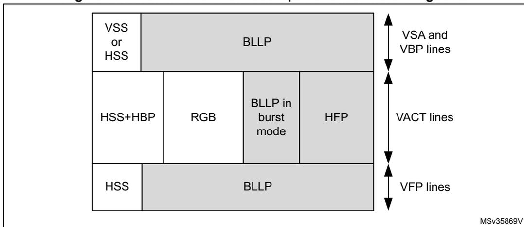
Commands are transmitted in the blanking periods after the following packets/states:
- • Vertical Sync Start (VSS) packets, if the video sync pulses are not enabled
- • Horizontal sync end (HSE) packets, in the VSA, VBP, and VFP regions
- • Horizontal sync Start (HSS) packets, if the video sync pulses are not enabled in the VSA, VBP, and VFP regions
- • Horizontal active (HACT) state
Besides the areas corresponding to BLLP, large commands can also be sent during the last line of a frame. In that case, the line time for the video mode is violated and the edpihalt signal is set to request the DPI video timing signals to remain inactive. Only if a command does not fit into any BLLP area, it is postponed to the last line, causing the violation of the line time for the video mode, as illustrated in Figure 428 .
Figure 428. Transmission of commands on the last line of a frame
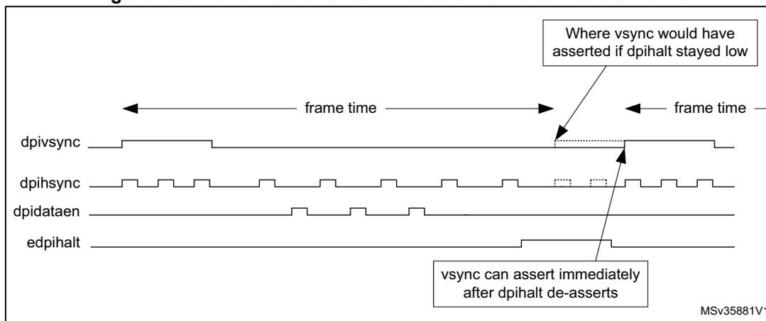
Where vsync would have asserted if dpivsync stayed low
frame time
frame time
dpivsync
dpihsync
dpidataen
edpihalt
vsync can assert immediately after dpivsync de-asserts
MSV35881V1
Only one command is transmitted per line, even in the case of the last line of a frame but one command is possible for each line.
There can be only one command sent in low-power per line. However, one low-power command is possible for each line. In high-speed, the DSI Host can send more than one command, as many as it determines to fit in the available time.
The DSI Host avoids sending commands in the last line because it is possible that the last line is shorter than the other ones. For instance, the line time ( \( t_L \) ) can be half a cycle longer than the \( t_L \) on the LTDC interface, that is, each line in the frame taking half a cycle from time for the last line. This results in the last line being \( (\frac{1}{2} \text{ cycle}) \times (\text{number of lines} - 1) \) shorter than \( t_L \) .
The COLM and SHTDN bits of the DSI Wrapper control register (DSI_WCR) are also able to trigger the sending of command packets. The commands are:
- • Color mode ON
- • Color mode OFF
- • Shut down peripheral
- • Turn on peripheral
These commands are not sent in the VACT region. If the low-power command enable (LPCE) bit of the DSI Host video mode configuration register (DSI_VMCR) is set, these commands are sent in low-power mode.
In low-power mode, the largest packet size (LPSIZE) field of the DSI Host low-power mode configuration register (DSI_LPMCR) is used to determine if these commands can be transmitted. It is assumed that largest packet size (LPSIZE) is greater than or equal to four bytes (number of bytes in a short packet), because the DSI Host does not transmit these commands on the last line.
If the frame bus-turn-around acknowledge enable (FBTAEE) bit is set in the DSI Host low-power mode configuration register (DSI_LPMCR), a BTA is generated by DSI Host after the last line of a frame. This may coincide with a write command or a read command. In either case, the LTDC interface is halted until an acknowledge is received (control of the DSI bus is returned to the host).
44.9.2 Transmission of commands in low-power mode
DSI Host can be configured to send the low-power commands during the high-speed video mode transmission.
To enable this feature, set the Low Power command enable (LPCE) bit of the DSI Host video mode configuration register (DSI_VMCR) to 1. In this case, it is necessary to calculate the time available, in bytes, to transmit a command in low-power mode to horizontal front-porch (HFP), vertical sync active (VSA), vertical back-porch (VBP), and vertical front-porch (VFP) regions.
Bits 8 to 13 of the video mode configuration register (DSI_VMCR) indicate if DSI Host can go to LP when idle. If the low-power command enable (LPCE) bit is set and non-video packets are in queue, DSI Host ignores the low-power configuration and transmits low-power commands, even if it is not allowed to enter low-power mode in a specific region. After the low-power commands transmission, DSI Host remains in low-power until a sync event occurs.
For example, consider that the VFP is selected as high-speed region (LPVFPE = 1'b0) with LPCE set as a command to transmit in low-power in the VPF region. This command is transmitted in low-power, and the line stays in low-power mode until a new HSS arrives.
Calculating the time to transmit commands in LP mode in the VSA, VBP, and VFP regions
The largest packet size (LPSIZE) field of the DSI Host low-power mode configuration register (DSI_LPMCR) indicates the time available (in bytes) to transmit a command in low-power mode (based on the escape clock) on a line during the VSA, VBP, and the VFP regions.
Calculation of largest packet size (LPSIZE) depends on the used video mode.
Figure 429 illustrates the timing intervals for the video mode in non-burst with sync pulses, while Figure 430 refers to video mode in burst and non-burst with sync events.
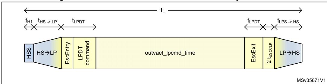
Figure 429. LPSIZE for non-burst with sync pulses
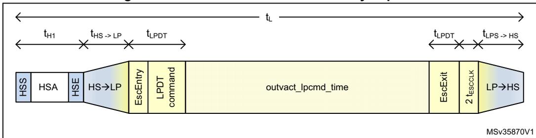
This timing diagram illustrates the sequence of events for a non-burst mode with sync pulses. It shows the transition from High-Speed (HS) to Low-Power (LP) and back. The sequence starts with HSS, HSA, and HSE. Then it transitions from HS to LP (t HS → LP ), followed by EscEntry, LPDT command, a period of outvact_lpcmd_time, EscExit, 2 t ESCCLK , and finally a transition from LP to HS (t LPS → HS ). Time intervals are marked as t H1 , t HS → LP , t LPDT , and t LPS → HS . The total line duration is labeled t L . The diagram is labeled MSV35870V1.
Figure 430. LPSIZE for burst or non-burst with sync events
This timing diagram illustrates the sequence of events for burst or non-burst mode with sync events. It shows the transition from High-Speed (HS) to Low-Power (LP) and back. The sequence starts with HSS, then transitions from HS to LP (t HS → LP ), followed by EscEntry, LPDT command, a period of outvact_lpcmd_time, EscExit, 2 t ESCCLK , and finally a transition from LP to HS (t LPS → HS ). Time intervals are marked as t H1 , t HS → LP , t LPDT , and t LPS → HS . The total line duration is labeled t L . The diagram is labeled MSV35871V1.
This time is calculated as follows:
\( LPSIZE = (t_L - (t_{H1} + t_{HS \rightarrow LP} + t_{LPHS} + t_{LPDT} + 2 t_{ESCCCLK})) / (2 \times 8 \times t_{ESCCCLK}) \) , where
- • \( t_L \) = line time
- • \( t_{H1} \) = time of the HSA pulse for sync pulses mode ( Figure 429 ) or time to send the HSS packet, including EoTp ( Figure 430 )
- • \( t_{HS \rightarrow LP} \) = time to enter the low-power mode
- • \( t_{LP \rightarrow HS} \) = time to leave the low-power mode
- • \( t_{LPDT} \) = D-PHY timing related with escape mode entry, LPDT command, and escape exit. According to the D-PHY specification, this value is always 11 bits in LP (or 22 TX escape clock cycles)
- • \( t_{ESCCCLK} \) = escape clock period as programmed in the TXECKDIV field of the DSI_CCR register
- • \( t_{ESCCCLK} \) = delay imposed by the DSI Host implementation.
In the above equation, division by eight is done to convert the available time to bytes. Division by two is done because one bit is transmitted every two escape clock cycles. The largest packet size (LPSIZE) field can be compared directly with the size of the command to be transmitted to determine if there is enough time to transmit the command. The maximum size of a command that can be transmitted in low-power mode is limited to 255 bytes by this field. Program this register to a value greater than or equal to 4 bytes for the transmission of the DCTRL commands, such as shutdown and color in low-power mode.
Consider an example of a frame with 12.4 \( \mu\text{s} \) per line and assume an escape clock frequency of 20 MHz and a lane bit rate of 800 Mbit/s. In this case, it is possible to send 124 bits in escape mode (that is, \( 124 \text{ bit} = 12.4 \mu\text{s} \times 20 \text{ MHz} / 2 \) ). Still, you need to consider the D-PHY protocol and PHY timings.
The following assumptions are made:
- • lane byte clock period is 10 ns (800 Mbit/s per lane)
- • escape clock period is 50 ns (DSI_CCR.TXECKDIV = 5)
- • video is transmitted in non-burst mode with sync pulses bounded by HSS and HSE packets
- • DSI is configured for two lanes
- • D-PHY takes 180 ns to transit from low-power to high-speed mode (DSI_DLTCCR.LS2HS_TIME = 18)
- • D-PHY takes 200 ns to transit from high-speed to low-power mode (DSI_DLTCCR.HS2LP_TIME = 20)
- • \( t_{HSA} = 420 \text{ ns} \) .
In this example, a 13-byte command can be transmitted as follows:
\( LPSIZE = (12.4 \mu\text{s} - (420 \text{ ns} + 180 \text{ ns} + 200 \text{ ns} + (22 \times 50 \text{ ns} + 2 \times 50 \text{ ns}))) / (2 \times 8 \times 50 \text{ ns}) = 13 \text{ bytes} \) .
Calculating the time to transmit commands in low-power mode in HFP region
The VACT largest packet size (VLPSIZE) field of the DSI Host low-power mode configuration register (DSI_LPMCR) indicates the time available (in bytes) to transmit a command in low-power mode (based on the escape clock) in the vertical active (VACT) region.
To calculate the value of VACT largest packet size (VLPSIZE), consider the video mode being used. Figure 431 shows the timing intervals for video mode in non-burst with sync pulses, Figure 432 those for video mode in non-burst with sync events, and Figure 433 refers to the burst video mode.
Figure 431. VLPSIZE for non-burst with sync pulses
Figure 432. VLPSIZE for non-burst with sync events
Figure 433. VLPSIZE for burst mode
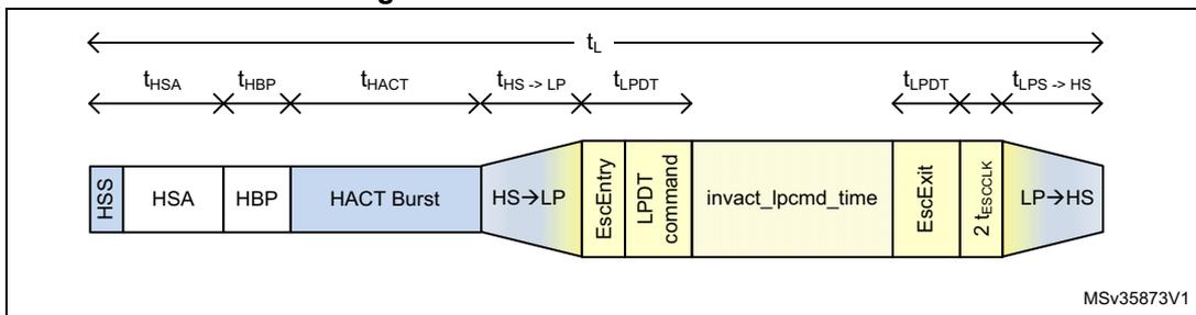
This time is calculated as follows:
where
- • \( t_L \) = line time
- • \( t_{HSA} \) = time of the HSA pulse (DSI_VHSACR.HSA)
- • \( t_{HBP} \) = time of horizontal back-porch (DSI_VHBPOR.HBP)
- • \( t_{HACT} \) = time of video active. For burst mode, the video active is time compressed and is calculated as \( t_{HACT} = VPSIZE * Bytes\_per\_Pixel / Number\_Lanes * t_{Lane\_byte\_clk} \)
- • \( t_{ESCCLK} \) = escape clock period as programmed in TXECKDIV field of the DSI_CCR register.
The VLPSIZE field can be compared directly with the size of the command to be transmitted to determine if there is time to transmit the command.
Consider an example of a frame with 16.4 \( \mu\text{s} \) per line and assume an escape clock frequency of 20 MHz and a lane bit rate of 800 Mbits/s. In this case, it is possible to send 420 bits in escape mode (that is, \( 164 \text{ bits} = 16.4 \mu\text{s} \times 20 \text{ MHz} / 2 \) ). Still, since it is the vertical active region of the frame, consider the HSA, HBP, and HACT timings apart from the D-PHY protocol and PHY timings. The following assumptions are made:
- • number of active lanes is four
- • Lane byte clock period (lanebyteclkperiod) is 10 ns (800 Mbit/s per lane)
- • escape clock period is 50 ns (DSI_CCR.TXECKDIV = 5)
- • D-PHY takes 180 ns to pass from low-power to high-speed mode (DSI_DLTCCR.LP2HS_TIME = 18)
- • D-PHY takes 200 ns to pass from high-speed to low-power mode (DSI_DLTCCR.HS2LP_TIME = 20)
- • \( t_{\text{HSA}} = 420 \text{ ns} \)
- • \( t_{\text{HBP}} = 800 \text{ ns} \)
- • \( t_{\text{HACT}} = 12800 \text{ ns} \) to send 1280 pixel at 24 bpp
- • video is transmitted in non-burst mode
- • DSI is configured for four lanes.
In this example, consider that video is sent in non-burst mode. The VLPSIZE is calculated as follows:
Only one byte can be transmitted in this period. A short packet (for example, generic short write) requires a minimum of four bytes. Therefore, in this example, commands are not sent in the VACT region.
If burst mode is enabled, more time is available to transmit the commands in the VACT region, because HACT is time compressed.
For burst mode, the VLPSIZE is 5 bytes and then a 4-byte short packet can be sent.
Transmission of commands in different periods
The LPSIZE and VLPSIZE fields allow a simple comparison to determine if a command can be transmitted in any of the BLLP periods.
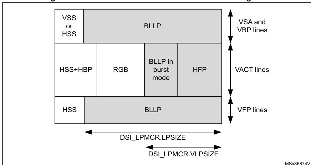
Figure 434 illustrates the meaning of VLPSIZE and LPSIZE, matching them with the shaded areas and the VACT region.
Figure 434. Location of LPSIZE and VLPSIZE in the image area
44.9.3 Transmission of commands in high-speed
If the LPCE bit of the DSI_VMCR register is 0, the commands are sent in high-speed video mode. In this case, the DSI Host automatically determines the area where each command can be sent and no programming or calculation is required.
44.9.4 Read command transmission
The MRD_TIME field of the DSI_DLTRCR register configures the maximum amount of time required to perform a read command in lane byte clock cycles, it is calculated as:
MRD_TIME = time to transmit the read command in low-power mode + time to enter and leave low-power mode + time to return the read data packet from the peripheral device.
The time to return the read data packet from the peripheral depends on the number of bytes read and the escape clock frequency of the peripheral, not the escape clock of the host. The MRD_TIME field is used in both high-speed and low-power mode to determine if there is time to complete a read command in a BLLP period.
In high-speed mode (LPCE = 0), MRD_TIME is calculated as follows:
In low-power mode (LPCE = 1), MRD_TIME is calculated as follows:
- • \( t_{\text{HS}\rightarrow\text{LP}} \) = time to enter the low-power mode
- • \( t_{\text{LP}\rightarrow\text{HS}} \) = time to leave the low-power mode
- • \( t_{\text{LPDT}} \) = D-PHY timing related to escape mode entry, LPDT command, and escape mode exit (according to the D-PHY specification, this value is always 11 bits in LP, or 22 TX escape clock cycles)
- • \( t_{\text{lprd}} \) = read command time in low-power mode ( \( 64 \times \text{TX esc clock} \) )
- • \( t_{\text{read}} \) = time to return the read data packet from the peripheral
- • \( t_{\text{BTA}} \) = time to perform a bus-turn-around (D-PHY dependent).
Keep the maximum number of bytes read from the peripheral to a minimum, to issue the read commands in a line time. Ensure that \( MRD\_TIME \times \text{lane byte clock period} \) is less than \( LPSIZE \times 16 \times \text{escape clock period of the host} \) , otherwise, the read commands are dispatched on the last line of a frame. If it is necessary to read a large number of parameters ( \( > 16 \) ), increase the \( MRD\_TIME \) while the read command is executed. When the read has completed, decrease the \( MRD\_TIME \) to a lower value.
If a read command is issued on the last line of a frame, the LTDC interface is halted and stays halted until the read command is in progress. The video transmission must be stopped during this period.
44.9.5 Clock lane in low-power mode
To reduce the power consumption of the D-PHY, the DSI Host, when not transmitting in the high-speed mode, allows the clock lane to enter into the low-power mode. The controller automatically handles the transition of the clock lane from HS (clock lane active sending clock) to LP state without direct intervention by the software. This feature can be enabled by configuring the DPCC and the ACR bits of the DSI_CLCR register.
In the command mode, the DSI Host can put the clock lane in the low-power mode when it does not have any HS packets to transmit.
In the video mode (LTDC interface), the DSI Host controller uses its internal video and PHY timing configurations to determine if there is time available for the clock line to enter the low-power mode and not compromise the video data transmission of pixel data and sync events.
Along with a correct configuration of the video mode (see Section 44.5: Functional description: video mode on LTDC interface ), the DSI Host needs to know the time required by the clock lane to go from high-speed to low-power mode and vice-versa. The values required can be obtained from the D-PHY specification: program the DSI_CLTCR register with the following values:
- • \( HS2LP\_TIME \) = time from HS to LP in clock lane / byte clock period in HS (lanebyteclk)
- • \( LP2HS\_TIME \) = time from LP to HS in clock lane / byte clock period in HS (lanebyteclk)
Based on the programmed values, the DSI Host calculates if there is enough time for the clock lane to enter the low-power mode during inactive regions of the video frame.
The DSI Host decides the best approach to follow regarding power saving out of the three possible scenarios:
- • there is no enough time to go to the low-power mode. Therefore, blanking period is added as shown in Figure 435
- • there is enough time for the data lanes to go to the low-power mode but not enough time for the clock lane to enter the low-power mode, see Figure 436 .
- • there is enough time for both data lanes and clock lane to go to the low-power mode, as in Figure 437 .
Figure 435. Clock lane and data lane in HS

The diagram shows a horizontal bar representing a video frame. It is divided into three segments: a purple segment on the left labeled 'HS', a large green segment in the middle labeled 'Blanking', and a purple segment on the right labeled 'HS'. Below the bar, there are two labels: 'Clock Lane in HS' and 'Data Lanes in HS', indicating that both the clock lane and data lanes are in high-speed mode throughout the frame, including the blanking period.
Figure 436. Clock lane in HS and data lanes in LP
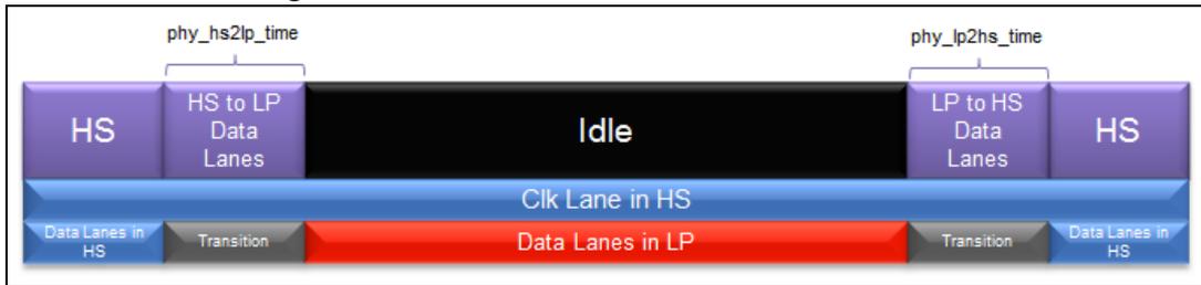
This diagram illustrates the timing sequence for a DSI interface where the clock lane is in High-Speed (HS) mode and data lanes are in Low-Power (LP) mode. The sequence starts with an HS state, followed by an 'HS to LP Data Lanes' transition (governed by \( phy\_hs2lp\_time \) ), then an Idle state, followed by an 'LP to HS Data Lanes' transition (governed by \( phy\_lp2hs\_time \) ), and finally returning to an HS state. Below this, the 'Clk Lane in HS' is shown as a continuous blue signal. The 'Data Lanes in LP' are shown as a red signal that is active during the Idle state and transitions during the 'HS to LP Data Lanes' and 'LP to HS Data Lanes' phases. The 'Data Lanes in HS' are shown as blue signals at the beginning and end of the sequence, separated by 'Transition' phases.
Figure 437. Clock lane and data lane in LP
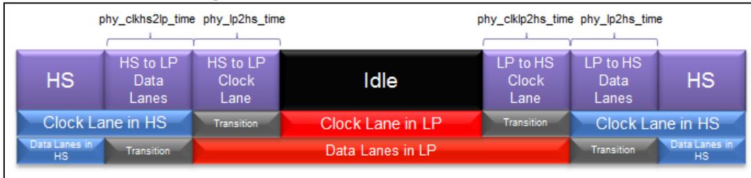
This diagram illustrates the timing sequence for a DSI interface where both the clock lane and data lanes are in Low-Power (LP) mode. The sequence starts with an HS state, followed by 'HS to LP Data Lanes' ( \( phy\_hs2lp\_time \) ) and 'HS to LP Clock Lane' ( \( phy\_lp2hs\_time \) ) transitions, then an Idle state, followed by 'LP to HS Clock Lane' ( \( phy\_clk2hs\_time \) ) and 'LP to HS Data Lanes' ( \( phy\_lp2hs\_time \) ) transitions, and finally returning to an HS state. Below this, the 'Clock Lane in HS' is shown as a blue signal that transitions to 'Clock Lane in LP' (red) during the Idle state. The 'Data Lanes in LP' are shown as a red signal that is active during the Idle state. The 'Data Lanes in HS' are shown as blue signals at the beginning and end of the sequence, separated by 'Transition' phases.
44.10 Functional description: virtual channels
The DSI Host supports choosing the virtual channel (VC) for use for each interface. Using multiple virtual channels, the system can address multiple displays at the same time, when each display has a different virtual channel identifier.
When the LTDC interface is configured for a particular virtual channel, it is possible to use the APB register interface to issue the commands while the video stream is being transmitted. With this, it is possible to send the commands through the ongoing video stream, addressing different virtual channels and thus enable the interface with multiple displays. During the video mode, the video stream transmission has the maximum priority. Therefore, the transmission of sideband packets such as the ones from the generic interface are only transported when there is time available within the video stream transmission. The DSI Host identifies the available time periods and uses them to transport the generic interface packets. Figure 438 illustrates where the DSI Host inserts the packets from the APB generic interface within the video stream transmitted by the LTDC interface.
Figure 438. Command transmission by the generic interface
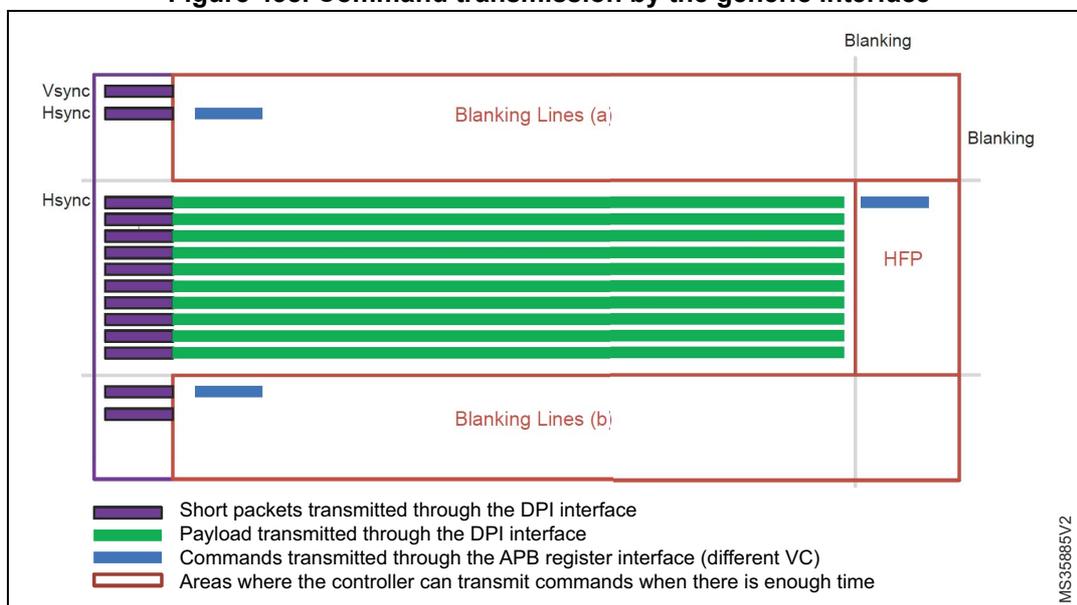
The diagram illustrates the timing of a video signal with Vsync and Hsync lines. It shows two blanking intervals, 'Blanking Lines (ai)' and 'Blanking Lines (bi)'. The 'HFP' (Horizontal Front Porch) area is marked. The legend indicates:
- Short packets transmitted through the DPI interface (purple bars)
- Payload transmitted through the DPI interface (green bars)
- Commands transmitted through the APB register interface (different VC) (blue bars)
- Areas where the controller can transmit commands when there is enough time (red outlines)
It is also possible to address the multiple displays with only the generic interface, using different virtual channels. Because the generic interface is not restricted to any particular virtual channel through configuration, it is possible to issue the packets with different virtual channels. This enables the interface to time multiplex the packets to be provided to the displays with different virtual channels.
You can use the following configuration registers to select the virtual channel ID associated with transmissions over the LTDC and APB register interfaces:
- • DSI_LVCDR.VCID field configures the virtual channel ID that is indexed to the video mode packets using the LTDC interface.
- • DSI_GHCR register configures the packet header (which includes the virtual channel ID to be used) for transmissions using APB register interface.
- • DSI_GVCIDR register configures the virtual channel ID of the read responses to store and return to the generic interface.
44.11 Functional description: video mode pattern generator
The video mode pattern generator allows the transmission of horizontal/vertical color bar and D-PHY BER testing pattern without any stimuli.
The frame requirements must be defined in video registers that are listed in Table 441 .
Table 441. Frame requirement configuration registers
| Register name | Description |
|---|---|
| DSI Host video mode configuration | Video mode configuration |
| DSI Host video packet configuration | Video packet size |
| DSI Host video chunks configuration | Number of chunks |
| DSI Host video null packet configuration | Null packet size |
| DSI Host video HSA configuration | Horizontal sync active time |
| DSI Host video HBP configuration | Horizontal back-porch time |
| DSI Host video line configuration | Line time |
| DSI Host video VSA configuration | Vertical sync active period |
| DSI Host video VBP configuration | Vertical back-porch period |
| DSI Host video VFP configuration | Vertical front-porch period |
| DSI Host video VA configuration | Vertical resolution |
44.11.1 Color bar pattern
The color bar pattern comprises eight bars for white, yellow, cyan, green, magenta, red, blue, and black colors.
Each color width is calculated by dividing the line pixel size (vertical pattern) or the number of lines (horizontal pattern) by eight. In the vertical color bar mode ( Figure 439 ), each single color bar has a width of the number of pixels in a line divided by eight. In case the number of pixels in a line is not divisible by eight, the last color (black) contains the remaining.
In the horizontal color bar mode ( Figure 440 ), each color line has a color width of the number of lines in a frame divided by eight. In case the number of lines in a frame is not divisible by eight, the last color (black) contains the remaining lines.
Figure 439. Vertical color bar mode

A diagram illustrating the vertical color bar mode. It consists of a rectangular frame containing eight vertical color bars of equal width. From left to right, the colors are: white, yellow, cyan, green, magenta, red, blue, and black. The bars are arranged side-by-side across the width of the frame.
Figure 440. Horizontal color bar mode

A diagram illustrating the horizontal color bar mode. It consists of a rectangular frame containing eight horizontal color bars of equal height. From top to bottom, the colors are: white, yellow, cyan, green, magenta, red, blue, and black. The bars are stacked vertically, filling the height of the frame.
44.11.2 Color coding
Table 442 shows the RGB components used.
Table 442. RGB components
| White | Yellow | Cyan | Green | Magenta | Red | Blue | Black | |
|---|---|---|---|---|---|---|---|---|
| R | High | High | Low | Low | High | High | Low | Low |
| G | High | High | High | High | Low | Low | Low | Low |
| B | High | Low | High | Low | High | Low | High | Low |
44.11.3 BER testing pattern
The BER testing pattern simplifies conformance testing. This pattern tests the RX D-PHY capability to receive the data correctly. The following data patterns are required:
- • X bytes of 0xAA (high-frequency pattern, inverted)
- • X bytes of 0x33 (mid-frequency pattern)
- • X bytes of 0xF0 (low-frequency pattern, inverted)
- • X bytes of 0x7F (lone 0 pattern)
- • X bytes of 0x55 (high-frequency pattern)
- • X bytes of 0xCC (mid-frequency pattern, inverted)
- • X bytes of 0x0F (low-frequency pattern)
- • Y bytes of 0x80 (lone 1 pattern).
In most cases, Y is equal to X. However, depending on line length and the color coding used, Y may be different from X. With RGB888 color coding and horizontal resolution in multiples of eight, the pattern shown in Figure 441 appears on the DSI display.
Figure 441. RGB888 BER testing pattern

The figure illustrates a rectangular area containing eight vertical bars of varying grayscale intensities. From left to right, the bars are: medium-light gray, dark gray, light gray, medium gray, dark gray, light gray, black, and medium-dark gray. The bars are of equal width and are contained within a thin black border.
44.11.4 Video mode pattern generator resolution
Depending on the orientation, BER mode, and color coding, the smallest resolutions accepted by the video mode pattern generator are:
- • BER mode: 8x8
- • horizontal color bar mode: 8x8
- • vertical color bar mode: 8x8.
Vertical pattern
The width of each color bar is determined by the division of horizontal resolution (pixels) for eight test pattern colors. If the horizontal resolution is not divisible by eight, the last color (black) is extended to fill the resolution.
In the example in Figure 442 , the horizontal resolution is 103.
Figure 442. Vertical pattern (103x15)

The diagram shows a horizontal sequence of color bars. Below each color bar is a double-headed arrow indicating its width in pixels. The widths are: 12 (white), 12 (yellow), 12 (cyan), 12 (green), 12 (magenta), 12 (red), 12 (blue), 12 (black), and 7 (black). The total width is 103 pixels.
| Color | Width (pixels) |
|---|---|
| White | 12 |
| Yellow | 12 |
| Cyan | 12 |
| Green | 12 |
| Magenta | 12 |
| Red | 12 |
| Blue | 12 |
| Black | 12 |
| Black | 7 |
Horizontal pattern
The width of each color bar is determined by the division of the number of vertical resolution (lines) for eight test pattern colors. If the vertical resolution is not divisible by eight, the last color (black) is extended to fill the resolution, as shown in Figure 443 .
Figure 443. Horizontal pattern (103x15)
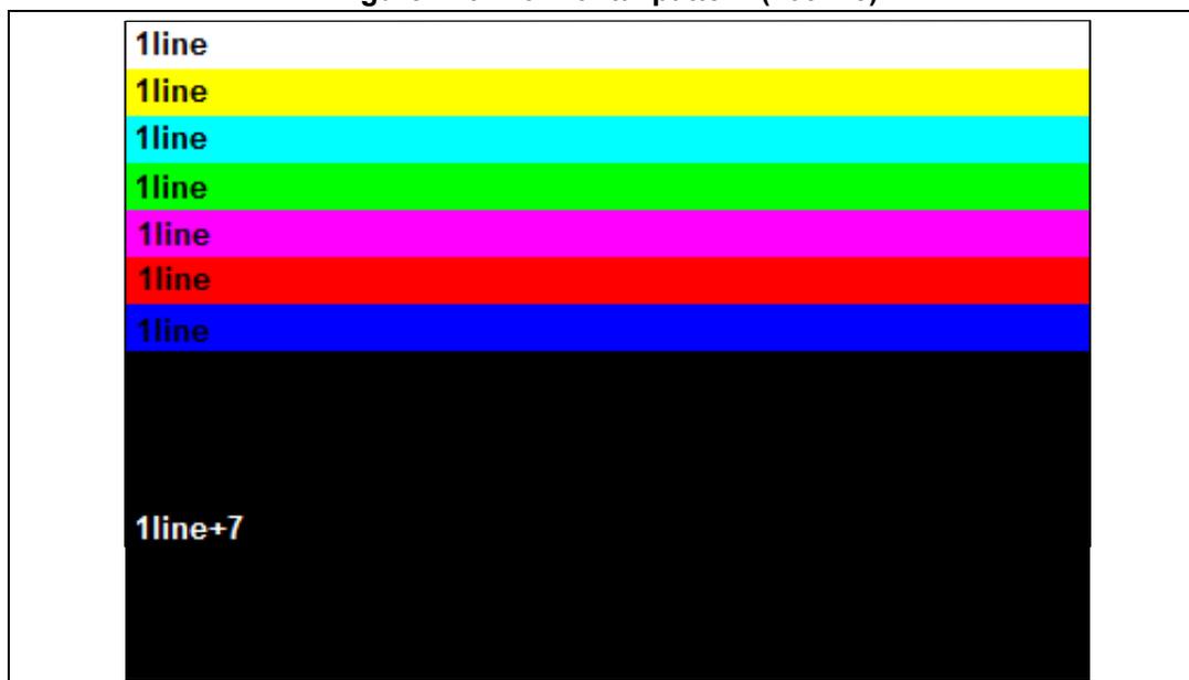
The diagram shows a vertical stack of color bars. To the left of each bar is a label indicating its height in lines. The heights are: 1line (white), 1line (yellow), 1line (cyan), 1line (green), 1line (magenta), 1line (red), 1line (blue), and 1line+7 (black). The total height is 15 lines.
| Color | Height (lines) |
|---|---|
| White | 1line |
| Yellow | 1line |
| Cyan | 1line |
| Green | 1line |
| Magenta | 1line |
| Red | 1line |
| Blue | 1line |
| Black | 1line+7 |
44.12 Functional description: D-PHY management
The embedded MIPI ® D-PHY is control directly by the DSI Host and is configured through the DSI Wrapper.
A dedicated PLL and a dedicated bias are also embedded to supply the clock and the power supply to the DSI and D-PHY.
44.12.1 D-PHY configuration
The D-PHY configuration is carried out through the DSI Wrapper, thanks to the DSI_WPCRx registers.
Slew-rate tuning on pins
To fine tune DSI communication, slew-rates can be adjusted:
- • clock slew rate for HS-TX speed through the DSI_DPCSRCR
- • data slew rate for HS-TX speed through the DSI_DPDL0SRCR and DSI_DPDL1SRCR
Band setting
The frequency band of the D-PHY is controlled by the DSI_DPCBCR register for the clock lane and by the DSI_DPDL0BCR and DSI_DPDL1BCR for the data lanes, it must be adjusted for clock and data lanes.
Custom lane configuration
To ease DSI integration, lane pins can be swapped on a lane as described in Table 443 .
Table 443. Custom lane configuration
| Function | Lane | Enable bit in DSI_WPCR0 |
|---|---|---|
| Swap lane pins | Clock lane | SWCL |
| Data lane 0 | SWDL0 | |
| Data lane 1 | SWDL1 |
44.12.2 D-PHY HS2LP and LP2HS durations
The DSI system is able to switch to LP mode during blanking period if there is enough time between two HS transmission.
To be able to make the scheduling and estimate if it is possible or not to make the switch, the duration of the transitions from HS to LP and from LP to HS must be programmed in the DSI Host in the DSI_CLTCR register for the clock lane and in the DSI_DLTCR register for the data lanes.
Table 444 gives an estimation of the values to be programmed for these timings, expressed in lane byte clock cycles.
Table 444. HS2LP and LP2HS values vs. band frequency (MHz)
| 80 to 100 | 100 to 120 | 120 to 160 | 160 to 200 | 200 to 240 | 240 to 320 | 320 to 390 | 390 to 450 | 450 to 510 | |
|---|---|---|---|---|---|---|---|---|---|
| Clock HS2LP | 4 + LPXO | 4 + LPXO | 5 + LPXO | 6 + LPXO | 7 + LPXO | 7 + LPXO | 9 + LPXO | 9 + LPXO | 11 + LPXO |
| Clock LP2HS | 8 + 3 * LPXO | 8 + 3 * LPXO | 14 + 3 * LPXO | 16 + 3 * LPXO | 21 + 3 * LPXO | 25 + 3 * LPXO | 32 + 3 * LPXO | 33 + 3 * LPXO | 40 + 3 * LPXO |
| Data HS2LP | 5 | 5 | 6 | 7 | 8 | 8 | 10 | 10 | 12 |
| Data LP2HS | 8 + 2 * LPXO | 9 + 2 * LPXO | 11 + 2 * LPXO | 14 + 2 * LPXO | 15 + 2 * LPXO | 17 + 2 * LPXO | 19 + 2 * LPXO | 20 + 2 * LPXO | 23 + 2 * LPXO |
44.12.3 Special D-PHY operations
The DSI Wrapper features some control bits to force the D-PHY in some particular state and/or behavior.
Forcing lane state
It is possible to force the data lane and/or the clock lane in TX stop mode through the bits FTXSMDL and FTXSMCL of the DSI_WPCR0 register. Setting these bits causes the respective lane module to immediately jump in transmit control mode and to begin transmitting a Stop state (LP-11).
This feature can be used to go back in TX mode after a wrong BTA sequence.
44.12.4 DSI PLL control
The dedicated DSI PLL is controlled through the DSI Wrapper, as shown in Figure 444 .
Figure 444. PLL block diagram
graph LR
    CLKIN[F_CLKIN
4 to 100 MHz] --> IDIV[9-bit
input divider
1/IDF]
    IDIV -->|F_PFD
2 to 100 MHz| PFD[PFD]
    PFD --> Filter[Filter]
    Filter --> VCO((Ring oscillator
F_VCO
500 to 1000 MHz))
    VCO --> ODIV[9-bit
output divider
1/ODF]
    ODIV --> PHI1[PHI1]
    VCO --> DIV2[1/2]
    DIV2 --> FDIV[9-bit
feedback divider
1/DIVN]
    FDIV --> PFD
The PLL output frequency is configured through the DSI_WRPCR register fields. The VCO frequency and the PLL output frequency are calculated as follows:
where:
- • \( CLK_{IN} \) is in the 4 to 100 MHz range
- • DSI_WRPCR.NDIV is in the 1 to 511 range
- • DSI_WRPCR.IDF is in the 1 to 511 range
- • \( F_{PFD} \) is in the 2 to 100 MHz range
- • \( F_{VCO} \) is in the 500 MHz to 1 GHz range
- • DSI_WRPCR.ODF can be 1 to 511
- • PHI is in the 31.25 to 500 MHz range
The PLL is enabled by setting the PLLEN bit in the DSI_WRPCR register.
Once the PLL is locked, the PLLLIF bit is set in the DSI_WISR. If the PLLIE bit is set in the DSI_WIER, an interrupt is generated.
The PLL status (lock or unlock) can be monitored with the PLLLS flag in the DSI_WISR register.
If the PLL gets unlocked, the PLLUIF bit of the DSI_WISR is set. If the PLLUIE bit of the DSI_WIER register is set, an interrupt is generated.
The DSI PLL settings can be changed only when the PLL is disabled.
44.12.5 D-PHY bias control
The bias providing the reference to the D-PHY is enabled setting the PWRUP bit of the DSI_BCFGGR register.
44.13 Functional description: interrupts and errors
The interrupts can be generated either by the DSI Host or by the DSI Wrapper.
All the interrupts are merged in one interrupt lane going to the interrupt controller.
44.13.1 DSI Wrapper interrupts
An interrupt can be produced on the following events:
- • tearing effect event
- • end of refresh
- • PLL locked
- • PLL unlocked
Separate interrupt enable bits are available for flexibility.
Table 445. DSI Wrapper interrupt requests
| Interrupt event | Event flag in DSI_WISR | Enable control bit in DSI_WIER |
|---|---|---|
| Tearing effect | TEIF | TEIE |
| End of refresh | ERIF | ERIE |
| PLL locked | PLLLIF | PLLLIE |
| PLL unlocked | PLLUIF | PLLUIE |
44.13.2 DSI Host interrupts and errors
The DSI_ISR0 and DSI_ISR1 registers are associated with error condition reporting. These registers can trigger an interrupt to inform the system about the occurrence of errors.
The DSI Host has one interrupt line that is set high when an error occurs in either the DSI_ISR0 or the DSI_ISR1 register.
The triggering of the interrupt can be masked by programming the mask registers DSI_IER0 and DSI_IER1. By default all errors are masked. When any bit of these registers is set to 1, it enables the interrupt for a specific error. The error bit is always set in the respective DSI_ISR register. The DSI_ISR0 and DSI_ISR1 registers are always cleared after a read operation. The interrupt line is cleared if all registers that caused the interrupt are read.
The interrupt force registers (DSI_FIR0 and DSI_FIR1) are used for test purposes: they allow triggering the interrupt events individually without the need to activate the conditions that trigger the interrupt sources (it is extremely complex to generate the stimuli for that purpose). This feature also facilitates the development and testing of the software associated with the interrupt events. Setting any bit of these registers to 1 triggers the corresponding interrupt.
The light yellow boxes in Figure 445 illustrate the location of some of the errors.
Figure 445. Error sources
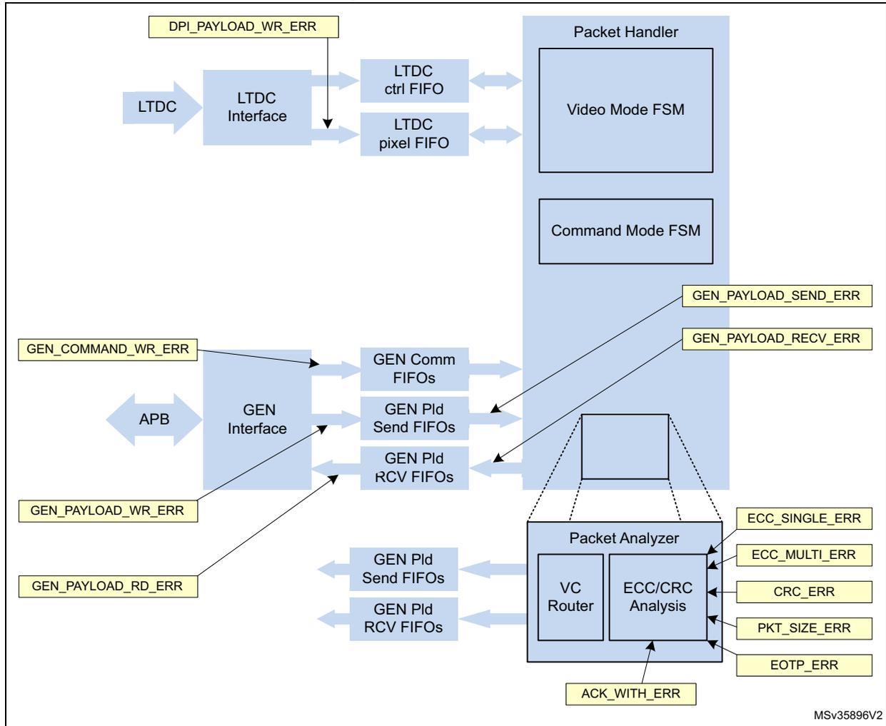
Table 446 explains the reasons that set off these interrupts and also explains how to recover from these interrupts.
Table 446. Error causes and recovery
| DSI Host interrupt and status register | Bit | Name | Error cause | Recommended method to handle the error |
|---|---|---|---|---|
| 0 | 20 | PE4 | The D-PHY reports the LP1 contention error. The D-PHY host detects the contention while trying to drive the line high. | Recover the D-PHY from contention. Reset the DSI Host and transmit the packets again. If this error is recurrent, carefully analyze the connectivity between the Host and the device. |
| 0 | 19 | PE3 | D-PHY reports the LP0 contention error. The D-PHY Host detects the contention while trying to drive the line low. | Recover the D-PHY from contention. Reset the DSI Host and transmit the packets again. If this error is recurrent, carefully analyze the connectivity between the Host and the device. |
Table 446. Error causes and recovery (continued)
| DSI Host interrupt and status register | Bit | Name | Error cause | Recommended method to handle the error |
|---|---|---|---|---|
| 0 | 18 | PE2 | The D-PHY reports the false control error. The D-PHY detects an incorrect line state sequence in lane 0 lines. | Device does not behave as expected, communication with the device is not properly established. This is an unrecoverable error. Reset the DSI Host and the D-PHY. If this error is recurrent, analyze the behavior of the device. |
| 0 | 17 | PE1 | The D-PHY reports the LPDT error. The D-PHY detects that the LDPT did not match a multiple of 8 bits. | The data reception is not reliable. The D-PHY recovers but the received data from the device might not be reliable. It is recommended to reset the DSI Host and repeat the RX transmission. |
| 0 | 16 | PE0 | The D-PHY reports the escape entry error. The D-PHY does not recognize the received escape entry code. | The D-PHY Host does not recognize the escape entry code. The transmission is ignored. The D-PHY Host recovers but the system must repeat the RX reception. |
| 0 | 15 | AE15 | This error is directly retrieved from acknowledge with error packet. The device detected a protocol violation in the reception. | Refer to the display documentation. When this error is active, the device must have another read-back command that reports additional information about this error. Read the additional information and take appropriate actions. |
| 0 | 14 | AE14 | The acknowledge with error packet contains this error. The device chooses to use this bit for error report. | Refer to the device documentation regarding possible reasons for this error and take appropriate actions. |
| 0 | 13 | AE13 | The acknowledge with error packet contains this error. The device reports that the transmission length does not match the packet length. | Possible reason for this is multiple errors present in the packet header (more than 2), so the error detection fails and the device does not discard the packet. In this case, the packet header is corrupt and can cause decoding mismatches. Transmit the packets again. If this error is recurrent, carefully analyze the connectivity between the Host and the device. |
| 0 | 12 | AE12 | The acknowledge with error packet contains this error. The device does not recognize the VC ID in at least one of the received packets. | Possible reason for this is multiple errors present in the packet header (more than 2), so the error detection fails and the device does not discard the packet. In this case, the packet header is corrupt and can cause decoding mismatches. Transmit the packets again. If this error is recurrent, carefully analyze the connectivity between the Host and the device. |
| 0 | 11 | AE11 | The acknowledge with error packet contains this error. The device does not recognize the data type of at least one of the received packets. | Check the device capabilities. It is possible that there are some packets not supported by the device. Repeat the transmission. |
Table 446. Error causes and recovery (continued)
| DSI Host interrupt and status register | Bit | Name | Error cause | Recommended method to handle the error |
|---|---|---|---|---|
| 0 | 10 | AE10 | The acknowledge with error packet contains this error. The device detects the CRC errors in at least one of the received packets. | Some of the long packets, transmitted after the last acknowledge request, might contain the CRC errors in the payload. If the payload content is critical, transmit the packets again. If this error is recurrent, carefully analyze the connectivity between the Host and the device. |
| 0 | 9 | AE9 | The acknowledge with error packet contains this error. The device detects multi-bit ECC errors in at least one of the received packets. | The device does not interpret the packets transmitted after the last acknowledge request. If the packets are critical, transmit the packets again. If this error is recurrent, carefully analyze the connectivity between the Host and the device. |
| 0 | 8 | AE8 | The acknowledge with error packet contains this error. The device detects and corrects the 1 bit ECC error in at least one of the received packets. | No action is required. The device acknowledges the packet. If this error is recurrent, analyze the signal integrity or the noise conditions of the link. |
| 0 | 7 | AE7 | The acknowledge with error packet contains this error. The device detects the line Contention through LP0/LP1 detection. | This error might corrupt the low-power data reception and transmission. Ignore the packets and transmit them again. The device recovers automatically. If this error is recurrent, check the device capabilities and the connectivity between the Host and device. Refer to section 7.2.1 of the DSI Specification 1.1. |
| 0 | 6 | AE6 | The acknowledge with error packet contains this error. The device detects the false control error. | The device detects one of the following: – The LP-10 (LP request) is not followed by the remainder of a valid escape or turnaround sequence. – The LP-01 (HS request) is not followed by a bridge state (LP-00). The D-PHY communications are corrupted. This error is unrecoverable. Reset the DSI Host and the D-PHY. Refer to the section 7.1.6 of the DSI Specification 1.1. |
Table 446. Error causes and recovery (continued)
| DSI Host interrupt and status register | Bit | Name | Error cause | Recommended method to handle the error |
|---|---|---|---|---|
| 0 | 5 | AE5 | The acknowledge with error packet contains this error. The display timeout counters for a HS reception and LP transmission expire. | It is possible that the Host and device timeout counters are not correctly configured. The device HS_TX timeout must be shorter than the Host HS_RX timeout. Host LP_RX timeout must be longer than the device LP_TX timeout. Check and confirm that the Host configuration is consistent with the device specifications. This error is automatically recovered, although there is no guarantee that all the packets in the transmission or reception are complete. For additional information about this error, see section 7.2.2 of the DSI Specification 1.1. |
| 0 | 4 | AE4 | The acknowledge with error packet contains this error. The device reports that the LPDT is not aligned in an 8-bit boundary | There is no guarantee that the device properly receives the packets. Transmit the packets again. For additional information about this error, see section 7.1.5 of the DSI Specification. |
| 0 | 3 | AE3 | The acknowledge with error packet contains this error. The device does not recognize the escape mode entry command. | The device does not recognize the escape mode entry code. Check the device capability. For additional information about this error, see section 7.1.4 of the DSI Specification. Repeat the transmission to the device. |
| 0 | 2 | AE2 | The acknowledge with error packet contains this error. The device detects the HS transmission did not end in an 8-bit boundary when the EoT sequence is detected. | There is no guarantee that the device properly received the packets. Re-transmission must be performed. Transmit the packets again. For additional information about this error, see section 7.1.3 of the DSI Specification 1.1. |
| 0 | 1 | AE1 | The acknowledge with error packet contains this error. The device detects that the SoT leader sequence is corrupted. | The device discards the incoming transmission. Re-transmission must be performed by the Host. For additional information about this error, see section 7.1.2 of the DSI Specification 1.1. |
| 0 | 0 | AE0 | The acknowledge with error packet contains this error. The device reports that the SoT sequence is received with errors but synchronization can still be achieved. | The device is tolerant to single bit and some multi-bit errors in the SoT sequence but the packet correctness is compromised. If the packet content was important, transmit the packets again. For additional information about this error, see section 7.1.1 of the DSI Specification 1.1. |
| 1 | 19 | PBUE | An underflow occurs in the LTDC payload buffer. | The LTDC frequency is too slow compared to the DSI bandwidth. Increase the LTDC frequency or decrease the DSI bandwidth. |
Table 446. Error causes and recovery (continued)
| DSI Host interrupt and status register | Bit | Name | Error cause | Recommended method to handle the error |
|---|---|---|---|---|
| 1 | 12 | GPRXE | An overflow occurs in the generic read FIFO. | The read FIFO size is not correctly dimensioned for the maximum read-back packet size. Configure the device to return the read data with a suitable size for the Host dimensioned FIFO. Data stored in the FIFO is corrupted. Reset the DSI Host and repeat the read procedure. |
| 1 | 11 | GPRDE | An underflow occurs in the generic read FIFO. | System does not wait for the read procedure to end and starts retrieving the data from the FIFO. The read data is requested before it is fully received. Data is corrupted. Reset the DSI Host and repeat the read procedure. Check that the read procedure is completed before reading the data through the APB interface. |
| 1 | 10 | GPTXE | An underflow occurs in the generic write payload FIFO. | The system writes the packet header before the respective packet payload is completely loaded into the payload FIFO. This error is unrecoverable, the transmitted packet is corrupted. Reset the DSI Host and repeat the write procedure. |
| 1 | 9 | GPWRE | An overflow occurs in the generic write payload FIFO. | The payload FIFO size is not correctly dimensioned to store the total payload of a long packet. Data stored in the FIFO is corrupted. Reset the DSI Host and repeat the write procedure. |
| 1 | 8 | GCWRE | An overflow occurs in the generic command FIFO. | The command FIFO size is not correctly dimensioned to store the total headers of a burst of packets. Data stored in the FIFO is corrupted. Reset the DSI Host and repeat the write procedure. |
| 1 | 7 | LPWRE | An overflow occurs in the DPI pixel payload FIFO. | The controller FIFO dimensions are not correctly set up for the operating resolution. Check the video mode configuration registers. They must be consistent with the LTDC video resolution. The pixel data sequence is corrupted. Reset the DSI Host and re-initiate the Video transmission. |
| 1 | 6 | EOTPE | Host receives a transmission that does not end with an end of transmission packet. | This error is not critical for the data integrity of the received packets. Check if the device supports the transmission of EoTp packets. |
Table 446. Error causes and recovery (continued)
| DSI Host interrupt and status register | Bit | Name | Error cause | Recommended method to handle the error |
|---|---|---|---|---|
| 1 | 5 | PSE | Host receives a transmission that does not end in the expected boundaries. | The integrity of the received data cannot be guaranteed. Reset the DSI Host and repeat the read procedure. |
| 1 | 4 | CRCE | Host reports that a received long packet has a CRC error in its payload. | The received payload data is corrupted. Reset the DSI Host and repeat the read procedure. If this error is recurrent, check the DSI connectivity link for the noise levels. |
| 1 | 3 | ECCME | Host reports that a received packet contains multiple ECC errors. | The received packet is corrupted. The DSI Host ignores all the following packets. The DSI Host must repeat the read procedure. |
| 1 | 2 | ECCSE | Host reports that a received packet contains a single bit error. | This error is not critical because the DSI Host can correct the error and properly decode the packet. If this error is recurrent, check the DSI connectivity link for signal integrity and noise levels. |
| 1 | 1 | TOLPRX | Host reports that the configured timeout counter for the low-power reception has expired. | Once the configured timeout counter ends, the DSI Host automatically resets the controller side and recovers to normal operation. Packet transmissions happening during this event are lost. If this error is recurrent, check the timer configuration for any issue. This timer must be greater than the maximum low-power transmission generated by the device. |
| 1 | 0 | TOHSTX | Host reports that the configured timeout counter for the high-speed transmission has expired. | Once the configured timeout counter ends, the DSI Host automatically resets the controller side and recovers to normal operation. Packet transmissions happening during this event are lost. If this error is recurrent, check the timer configuration for any issue. This timer must be greater than the maximum high-speed transmission bursts generated by the Host. |
| DSI Wrapper | 10 | PLLUF | The PLL of the D-PHY has unlocked. | This error can be critical. The graphical subsystem must be reconfigured and restarted. |
44.14 Programing procedure
To operate the DSI Host the user must be familiar with the MIPI® DSI specification. Every software programmable register is accessible through the APB interface.
44.14.1 Programing procedure overview
The procedure for video mode or adapted command mode must respect the following order:
- 1. Configure the LTDC (refer to LTDC section)
- a) Configure RCC for LTDC
- b) Configure the LTDC PLL, turn it ON, and wait for its lock
- c) Program the panel timings
- d) Enable the relevant layers
- 2. Configure the RCC for DSI (refer to RCC section)
- a) Configure PLL3, turn it on, and wait for its lock
- b) Keep the lane byte clock on PLL3 up and running
- c) Enable the clock for DSI
- 3. Optionally, configure the GPIO (if tearing effect requires GPIO usage for example or reset for display)
- 4. Optionally, reset display (when the display needs to be reset in LP-00)
- 5. Optionally, validate the ISR
- 6. Turn on the DSI bias (DSI_BCGGR.PWRUP = 1)
- 7. Configure the DSI PLL, turn it ON, and wait for its lock as described in Section 44.12.4
- 8. Enable DSI Host (DSI_CR.EN = 1)
- 9. Configure clock division factors (DSI_CCR.TXECKDIV \( \neq \) 0x0) to start tx_clk_esc clock (this clock is required to configure the D-PHY)
- 10. Configure the D-PHY parameters in the DSI Host, the DSI D-PHY, and in the DSI Wrapper to define D-PHY configuration and timing as described in Section 44.14.2
- 11. Enable the D-PHY setting the DEN bit of the DSI_PCTLR
- 12. Configure the band control (BC fields) and the slew rate (SRC fields) for the clock lane and the data lanes in DSI_DPCBCR, DSI_DPDLxBCD, DSI_DPCSRCR, and DSI_DPDLxSRCR
- 13. Enable the D-PHY clock lane setting the CKEN bit of the DSI_PCTLR
- 14. Switch the lane byte clock from PLL3 to D-PHY PLL in the RCC
- 15. Wait for the D-PHY to be in STOP state checking the bits:
- a) the clock lane stop state (PSSC) in the DSI_PSR
- b) data lanes stop state (PSS1/PSS0) in the DSI_PSR
- 16. Disable the DSI Host (DSI_CR.EN = 0)
- 17. Turn on clock lane in high speed as no automatic control (DPCC)
- 18. Configure the DSI Host timings as detailed in Section 44.14.3
- 19. Configure the DSI Host flow control and DBI interface as detailed in Section 44.14.4
- 20. Configure the DSI Host LTDC interface as detailed in Section 44.14.5
- 21. Configure the DSI Host for video mode as detailed in Section 44.14.6 or adapted command mode as detailed in Section 44.14.7
- 22. Optionally, reset display (when the display needs to be reset in LP-11)
- 23. Start the DSI (DSI_CR.EN = 1 and DSI_WCR.DSIEN = 1)
- 24. Optionally, send DCS commands through the APB generic interface to configure the display
- 25. Enable the LTDC in the LTDC
- 26. Start the LTDC flow through the DSI Wrapper (DSI_WCR.LTDCEN = 1)
- a) In video mode, the data streaming starts as soon as the LTDC is enabled
- a) In adapted command mode, the frame buffer update is launched as soon as the DSI_WCR.LTDCEN bit is set
44.14.2 Configuring the D-PHY parameters
The D-PHY requires a specific configuration prior starting any communications. The configuration parameters are stored either in the DSI Host or the DSI Wrapper.
Configuring the D-PHY parameters
The D-PHY must be configured to adjust:
- • the slew rate for the clock lane through register DSI_DPCSRC
- • the slew rate for the data lanes through DSI_DPDL0SRC and DSI_DPDL1SRC
- • the frequency band for the clock lane through DSI_DPCLBCR
- • the frequency band for the data lanes through DSI_DPDL0BCR and DSI_DPBL1BCR
Configuring the D-PHY parameters in the DSI Host
The DSI Host stores the configuration of D-PHY timing parameters and number of lanes.
The following fields must be configured prior to any startup:
- • Number of data lanes in the DSI_PCONF register
- • Automatic clock lane control (ACR) in the DSI_CLCR register
- • Clock control (DPCC) in the DSI_CLCR register
- • Time for LP/HS and HS/LP transitions for both clock lane and data lanes in DSI_CLTCR and DSI_DLTCR registers
- • Stop wait time in the DSI_PCONF register
44.14.3 Configuring the DSI Host timing
All the protocol timing must be configured in the DSI Host.
Clock divider configuration
Two clocks are generated internally, namely the timeout clock and the TX escape clock.
The timeout clock is used as the timing unit in the configuration of HS to LP and LP to HS transition error. Its division factor is configured by the timeout clock division (TOCKDIV) field of the DSI Host clock control register (DSI_CCR).
The TX escape clock is used in low-power transmission. Its division factor is configured by the TX escape clock division (TXECKDIV) field of the DSI Host clock control register (DSI_CCR) relatively to the lanebyteclock. Its typical value must be around 20 MHz.
Timeout configuration
The timings for timeout management as described in Section 44.8 are configured in the DSI Host timeout counter configuration registers (DSI_TCCR0 to DSI_TCCR5).
44.14.4 Configuring flow control and DBI interface
The flow control is configured thanks to the DSI Host protocol configuration register (DSI_PCR). The configuration parameters are the following
- • CRC reception enable (CRCRXE bit)
- • ECC reception enable (ECCRXE bit)
- • BTA enable (BTAE bit)
- • EoTp reception enable (ETRXE bit)
- • EoTp transmission enable (ETTXE bit)
Their values depend upon the protocol to be used for the communication with the DSI display.
The virtual channel ID used for the generic DBI interface must be configured by the virtual channel ID (VCID) field of the DSI Host generic VCID register (DSI_GVCIDR).
All the DCS command, depending on their type, can be transmitted or received either in high-speed or low-power. For each of them, a dedicated configuration bit must be programmed in the DSI Host command mode configuration register (DSI_CMCR).
Acknowledge request for packet or tearing effect event must also be configured in the DSI Host command mode configuration register (DSI_CMCR).
44.14.5 Configuring the DSI Host LTDC interface
As the DSI Host is interface to the system through the LTDC for video mode or adapted command mode, the DSI Wrapper performs a low level interfacing in between.
The parameter programmed into the DSI Wrapper must be aligned with the parameters programmed into the LTDC and the DSI Host.
The following fields must be configured:
- • Virtual channel ID in the virtual channel ID (VCID) field of the DSI Host LTDC VCID register (DSI_LVCIDR).
- • Color coding (COLC) field of the DSI Host LTDC color coding register (DSI_LCOLCR) and the color multiplexing (COLMUX) in the DSI Wrapper configuration register (DSI_WCFGR).
- • If loose packets are used for 18-bit mode, the loosely packet enable (LPE) bit of the DSI Host LTDC color coding register (DSI_LCOLCR) must be set.
44.14.6 Configuring the video mode
The video mode configuration defines the behavior of the controller in low-power for command transmission, the type of video transmission (burst or non-burst mode) and the panel horizontal and vertical timing:
- • Select the video transmission mode to define how the processor requires the video line to be transported through the DSI link.
- – Configure the low-power transitions in the DSI_VMCR to define the video periods, which are permitted to go to low-power if there is time available to do so.
- – Configure if the controller must request the peripheral acknowledge message at the end of frames (DSI_VMCR.FBTAAE).
- – Configure if commands are to be transmitted in low-power (DSI_VMCR.LPE).
- • Select the video mode type
- – Burst mode:
Configure the video mode type (DSI_VMCR.VMT) with value 2'b1x.
Configure the video packet size (DSI_VPCR.VPSIZE) with the size of the active line period, measured in pixels.
The registers DSI_VCCR and DSI_VNPCR are ignored by the DSI Host. - – Non-burst mode:
Configure the video mode type (DSI_VMCR.VMT) with 2'b00 to enable the transmission of sync pulses or with 2'b01 to enable the transmission of sync events.
Configure the video packet size (DSI_VPCR.VPSIZE) with the number of pixels to be transmitted in a single packet. Selecting this value depends on the available memory of the attached peripheral, if the data is first stored, or on the memory you want to select for the FIFO in DSI Host.
Configure the number of chunks (DSI_VCCR.NUMC) with the number of packets to be transmitted per video line. The value of VPSIZE * NUMC is the number of pixels per line of video, except if NUMC is 0, which disables the multi-packets. If you set it to 1, there is still only one packet per line, but it can be part of a chunk, followed by a null packet.
Configure the null packet size (DSI_VNPCR.NPSIZE) with the size of null packets to be inserted as part of the chunks. Setting it to 0 disables null packets.
- – Burst mode:
- • Define the video horizontal timing configuration as follows:
- – Configure the horizontal line time (DSI_VLCR.HLINE) with the time taken by an LTDC video line measured in cycles of lane byte clock (for a clock lane at 500 MHz the lane byte clock period is 8 ns). When the periods of LTDC clock and lane byte clock are not multiples, the value to program the DSI_VLCR.HLINE needs to be rounded. A timing mismatch is introduced between the lines due to the rounding of configuration values. If the DSI Host is configured not to go to low-power, this timing divergence accumulates on every line, introducing a significant amount of mismatch towards the end of the frame. The reason for this is that the DSI Host cannot resynchronize on every new line because it transmits the blanking packets when the horizontal sync event occurs on the LTDC interface. However, the accumulated mismatch must become extinct on the last line of a frame, where, according to the DSI specification, the link must always return to low-power regaining synchronization, when a new frame starts on a vertical sync event. If the accumulated timing mismatch is greater than the time in low-power on the last
line, a malfunction occurs. This phenomenon can be avoided by configuring the DSI Host to go to low-power once per line.
- – Configure the horizontal sync duration (DSI_VHSACR.HSA) with the time taken by an LTDC horizontal sync active period measured in cycles of lane byte clock (normally a period of 8 ns).
- – Configure the horizontal back-porch duration (DSI_VHBPCR.HBP) with the time taken by the LTDC horizontal back-porch period measured in cycles of lane byte clock (normally a period of 8 ns). Special attention must be given to the calculation of this parameter.
- • Define the vertical line configuration:
- – Configure the vertical sync duration (DSI_VVSACR.VSA) with the number of lines existing in the LTDC vertical sync active period.
- – Configure the vertical back-porch duration (DSI_VVBPCR.VBP) with the number of lines existing in the LTDC vertical back-porch period.
- – Configure the vertical front-porch duration (DSI_VVFPPCR.VFP) with the number of lines existing in the LTDC vertical front-porch period.
- – Configure the vertical active duration (DSI_VVACR.VA) with the number of lines existing in the LTDC vertical active period.
Figure 446 illustrates the steps for configuring the DPI packet transmission.
Figure 446. Video packet transmission configuration flow diagram
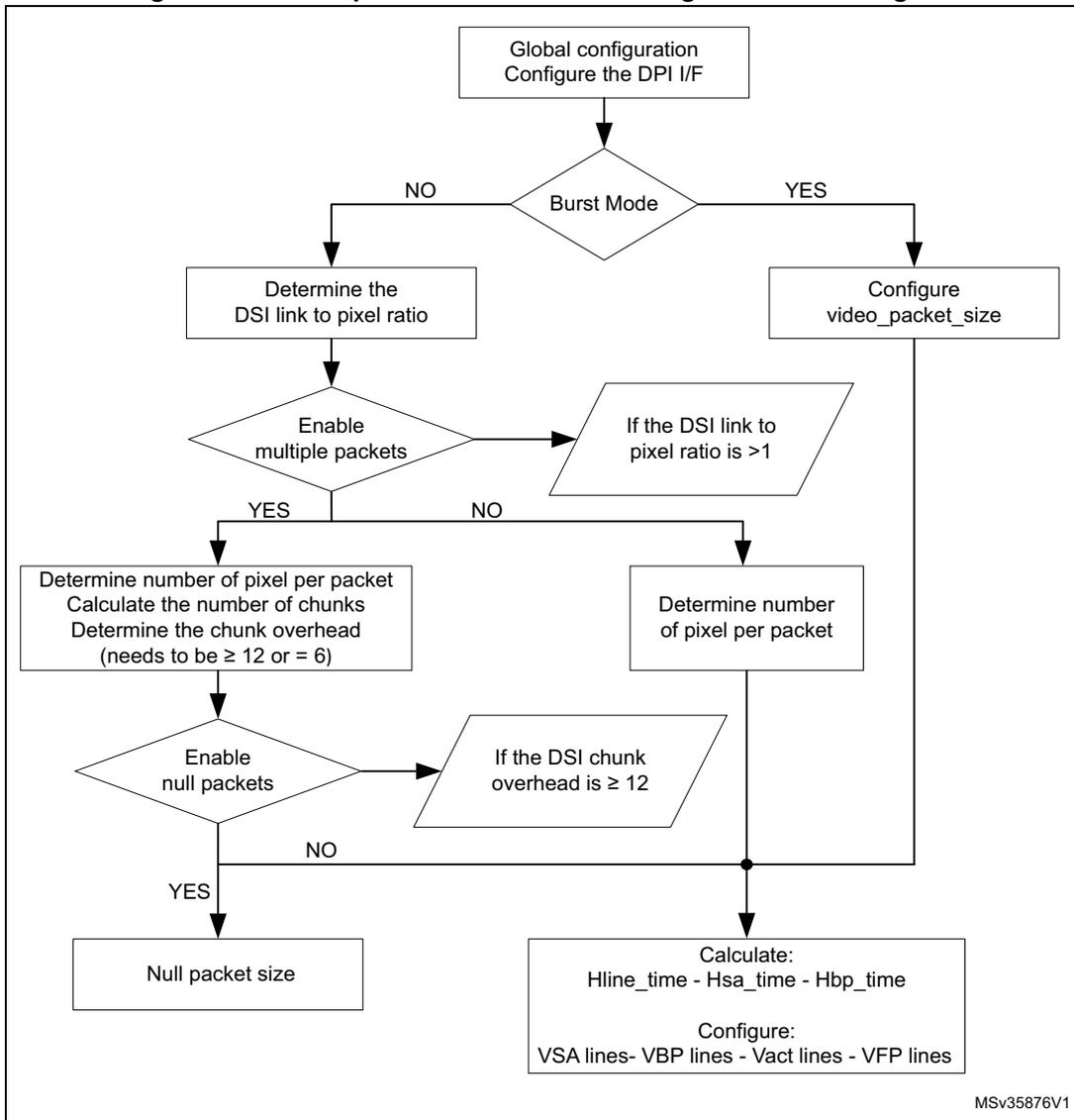
graph TD; A[Global configuration
Configure the DPI I/F] --> B{Burst Mode}; B -- NO --> C[Determine the
DSI link to pixel ratio]; B -- YES --> D[Configure
video_packet_size]; C --> E{Enable
multiple packets}; E -- YES --> F[Determine number of pixel per packet
Calculate the number of chunks
Determine the chunk overhead
(needs to be ≥ 12 or = 6)]; E -- NO --> G[Determine number
of pixel per packet]; E -- YES --> H{Enable
null packets}; H -- YES --> I[Null packet size]; H -- NO --> J(( )); H -- YES --> K[/If the DSI chunk
overhead is ≥ 12/]; F --> H; G --> J; D --> J; J --> L[Calculate:
Hline_time - Hsa_time - Hbp_time

Configure:
VSA lines- VBP lines - Vact lines - VFP lines];
MSV35876V1
Example of video configuration
The following is an example of video packet transmission configuration:
Video resolution:
- • PCLK period = 50 ns
- • HSA = 8 PCLK
- • HBP = 8 PCLK
- • HACT = 480 PCLK
- • HFP = 24 PCLK
- • VSA = 2 lines
- • VBP = 2 lines
- • VACT = 640 lines
- • VFP = 4 lines
Configuration steps:
- • Video transmission mode configuration:
- a) Configure the low-power transitions:
\( DSI\_VMCR[13:8] = 6'b111111 \) , to enable LP in all video period. - b) \( DSI\_VMCR.FBTAEE = 1 \) , for the DSI Host to request an acknowledge response message from the peripheral at the end of each frame.
- a) Configure the low-power transitions:
- • To use the burst mode, follow these steps:
\( DSI\_VMCR.VMT = 2'b1x \)
\( DSI\_VPCR.VPSIZE = 480 \) - • Horizontal timing configuration:
- – \( DSI\_VLCR.HLINE = (HSA + HBP + HACT + HFP) * (PCLK\ period / Clk\ lane\ byte\ period) = (8 + 8 + 480 + 24) * (50 / 8) = 3250 \)
- – \( DSI\_VHSACR.HSA = HSA * (PCLK\ period / Clk\ lane\ byte\ period) = 8 * (50 / 8) = 50 \)
- – \( DSI\_VHBPCR.HBP = HBP * (PCLK\ period / Clk\ lane\ byte\ period) = 8 * (50 / 8) = 50 \)
- • Vertical line configuration:
- – \( DSI\_VVSACR.VSA = 2 \)
- – \( DSI\_VVBPCR.VBP = 2 \)
- – \( DSI\_VVFPCR.VFP = 4 \)
- – \( DSI\_VVACR.VA = 640 \)
44.14.7 Configuring the adapted command mode
The adapted command mode requires the following parameters to be configured:
- • Command size (CMDSIZE) field of the DSI Host LTDC command configuration register (DSI_LCCR) to define the maximum allowed size for a write memory command.
- • The tearing effect source (TESRC) and optionally tearing effect polarity (TEPOL) bits of the DSI Wrapper configuration register (DSI_WCFGR).
- • The automatic refresh (AR) bit of the DSI Wrapper configuration register (DSI_WCFGR) if the display needs to be updated automatically each time a tearing effect event is received.
44.14.8 Configuring the video mode pattern generator
DSI Host can transmit a color bar pattern without horizontal/vertical color bar and D-PHY BER testing pattern without any kind of stimuli.
Figure 447 shows the programming sequence to send a test pattern:
- 1. Configure the DSI_MCR register to enable video mode. Configure the video mode type using DSI_VMCR.VMT.
- 2. Configure the DSI_LCOLCR register.
- 3. Configure the frame using registers shown in Figure 448 (where the gray area indicates the transferred pixels).
- 4. Configure the pattern generation mode (DSI_VMCR.PGM) and the pattern orientation (DSI_VMCR.PGO), and enable them (DSI_VMCR.PGE).
Figure 447. Programming sequence to send a test pattern
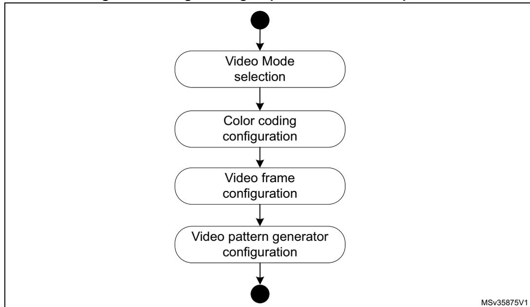
graph TD; Start(( )) --> A[Video Mode selection]; A --> B[Color coding configuration]; B --> C[Video frame configuration]; C --> D[Video pattern generator configuration]; D --> End(( ));
MSV35875V1
Figure 448. Frame configuration registers
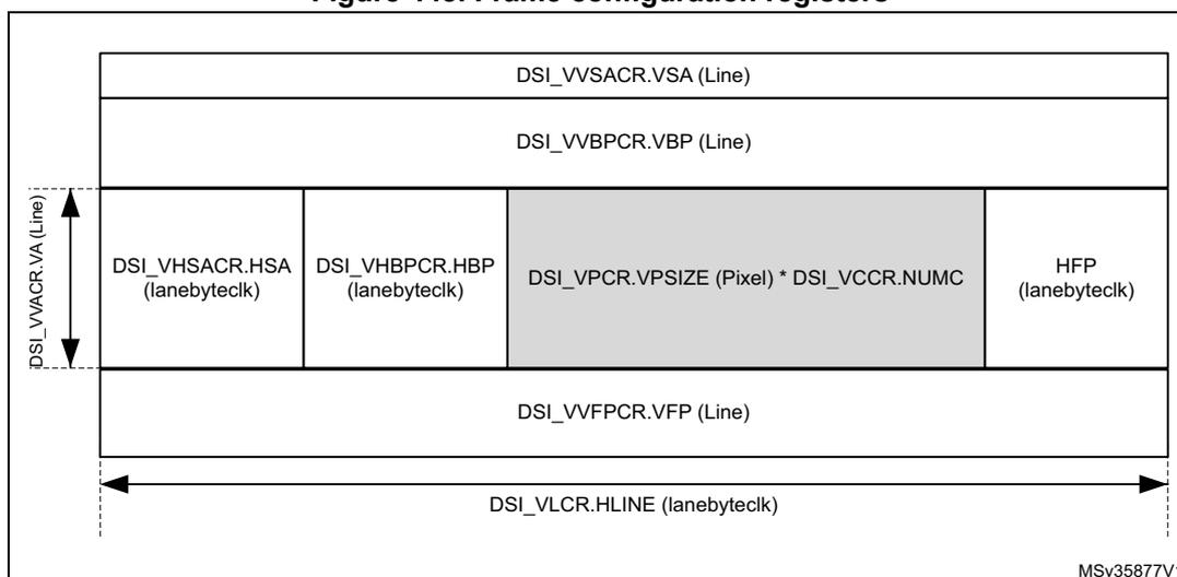
The diagram illustrates the structure of a video frame as defined by configuration registers. The frame is shown as a rectangle divided into several horizontal and vertical sections. The top section is labeled DSI_VVSACR.VSA (Line). Below it is DSI_VVBPCR.VBP (Line). The main body of the frame is divided into four horizontal segments: DSI_VHSA.CR.HSA (lanebyteclk), DSI_VHBP.CR.HBP (lanebyteclk), a large shaded area representing the payload (DSI_VPCR.VPSIZE (Pixel) * DSI_VCCR.NUMC), and HFP (lanebyteclk). The bottom section is labeled DSI_VVFP.CR.VFP (Line). A horizontal double-headed arrow at the bottom indicates the total horizontal length as DSI_VLCR.HLINE (lanebyteclk). A vertical double-headed arrow on the left indicates the total vertical length as DSI_VVACR.VA (Line). The diagram is labeled MSv35877V1 in the bottom right corner.
Note: The number of pixels of payload is restricted to a multiple of a value provided in Table 437 .
44.14.9 Managing ULPM
There are two ways to configure the software to enter and exit the ULPM:
- • enter and exit the ULPM with the D-PHY PLL running (a faster process)
- • enter and exit the ULPM with the D-PHY PLL turned off (a more efficient process in terms of power consumption).
Clock management for ULPM sequence
The ULPM management state machine is working on the lanebyteclock provided by the D-PHY.
Because the D-PHY is providing the lanebyteclock only when the clock lane is not in ULPM state, it is mandatory to switch the lanebyteclock source of the DSI Host before starting the ULPM mode entry sequence.
The lanebyteclock source is controlled by the RCC. It can be
- • the lanebyteclock provided by the D-PHY (for all modes except ULPM)
- • a clock generated by the system PLL (for ULPM)
Process flow to enter the ULPM
Implement the process described in detail in the following procedure to enter the ULPM on both clock lane and data lanes:
- 1. Verify the initial status of the DSI Host:
- – DSI_PCTLR[2:1] = 2'h3
- – DSI_WRPCR.PLLEN = 1'h1 and DSI_WRPCR.REGEN = 1'h1
- – DSI_PUCR[3:0] = 4'h0
- – DSI_PTTCR[3:0] = 4'h0
- – Verify that all active lanes are in Stop state and the D-PHY PLL is locked:
One-lane configuration: DSI_PSR[6:4] = 3'h3 and DSI_PSR[1] = 1'h0 and DSI_WISR.PLLS = 1'h1
Two-lanes configuration: DSI_PSR[8:4] = 5'h1B and DSI_PSR[1] = 1'h0 and DSI_WISR.PLLS = 1'h1
- 2. Switch the lanebyteclock source in the RCC from D-PHY to system PLL
- 3. Set DSI_PUCR[3:0] = 4'h5 to enter ULPM in the data and the clock lanes.
- 4. Wait until the D-PHY active lanes enter into ULPM:
- – One-lane configuration: DSI_PSR[6:1] = 6'h00
- – Two-lanes configuration: DSI_PSR[8:1] = 8'h00
- 5. Turn off the D-PHY PLL by setting DSI_WRPCR.PLLEN = 1'b0
Process flow to exit the ULPM
Implement the process flow described in the following procedure to exit the ULPM on both clock lane and data lanes:
- 1. Verify that all active lanes are in ULPM:
- – One-lane configuration: DSI_PSR[6:1] = 6'h00
- – Two-lanes configuration: DSI_PSR[8:1] = 8'h00
- 2. Turn on the D-PHY PLL by setting DSI_WRPCR.PLLLEN = 1'b1.
- 3. Wait until D-PHY PLL locked
- – DSI_WISR.PLLS = 1'b1
- 4. Without de-asserting the ULPM request bits, assert the exit ULPM bits by setting DSI_PUCR[3:0] = 4'hF.
- 5. Wait until all active lanes exit ULPM:
- – One-lane configuration:
DSI_PSR[5] = 1'b1
DSI_PSR[3] = 1'b1 - – Two-lanes configuration:
DSI_PSR[8] = 1'b1
DSI_PSR[5] = 1'b1
DSI_PSR[3] = 1'b1
- – One-lane configuration:
- 6. Wait for 1 ms.
- 7. De-assert the ULPM requests and the ULPM exit bits by setting DSI_PUCR [3:0] = 4'h0.
- 8. Switch the lanbyteclock source in the RCC from system PLL to D-PHY
- 9. The DSI Host is now in Stop state and the D-PHY PLL is locked:
- – One-lane configuration:
DSI_PSR[6:4] = 3'h3
DSI_PSR[1] = 1'h0
DSI_WRPCR.PLLLEN = 1'b1 - – Two-lanes configuration:
DSI_PSR[8:4] = 5'h1B
DSI_PSR[1] = 1'h0
DSI_WRPCR.PLLLEN = 1'b1
- – One-lane configuration:
44.15 DSI Host registers
44.15.1 DSI Host version register (DSI_VR)
Address offset: 0x0000
Reset value: 0x3134 312A
| 31 | 30 | 29 | 28 | 27 | 26 | 25 | 24 | 23 | 22 | 21 | 20 | 19 | 18 | 17 | 16 |
|---|---|---|---|---|---|---|---|---|---|---|---|---|---|---|---|
| VERSION[31:16] | |||||||||||||||
| r | r | r | r | r | r | r | r | r | r | r | r | r | r | r | r |
| 15 | 14 | 13 | 12 | 11 | 10 | 9 | 8 | 7 | 6 | 5 | 4 | 3 | 2 | 1 | 0 |
| VERSION[15:0] | |||||||||||||||
| r | r | r | r | r | r | r | r | r | r | r | r | r | r | r | r |
Bits 31:0 VERSION[31:0] : Version of the DSI Host
This read-only register contains the version of the DSI Host
44.15.2 DSI Host control register (DSI_CR)
Address offset: 0x0004
Reset value: 0x0000 0000
| 31 | 30 | 29 | 28 | 27 | 26 | 25 | 24 | 23 | 22 | 21 | 20 | 19 | 18 | 17 | 16 |
|---|---|---|---|---|---|---|---|---|---|---|---|---|---|---|---|
| Res. | Res. | Res. | Res. | Res. | Res. | Res. | Res. | Res. | Res. | Res. | Res. | Res. | Res. | Res. | Res. |
| 15 | 14 | 13 | 12 | 11 | 10 | 9 | 8 | 7 | 6 | 5 | 4 | 3 | 2 | 1 | 0 |
| Res. | Res. | Res. | Res. | Res. | Res. | Res. | Res. | Res. | Res. | Res. | Res. | Res. | Res. | Res. | EN |
| rw |
Bits 31:1 Reserved, must be kept at reset value.
Bit 0 EN : Enable
This bit configures the DSI Host in either power-up mode or to reset.
- 0: DSI Host disabled (under reset)
- 1: DSI Host enabled
44.15.3 DSI Host clock control register (DSI_CCR)
Address offset: 0x0008
Reset value: 0x0000 0000
| 31 | 30 | 29 | 28 | 27 | 26 | 25 | 24 | 23 | 22 | 21 | 20 | 19 | 18 | 17 | 16 |
|---|---|---|---|---|---|---|---|---|---|---|---|---|---|---|---|
| Res. | Res. | Res. | Res. | Res. | Res. | Res. | Res. | Res. | Res. | Res. | Res. | Res. | Res. | Res. | Res. |
| 15 | 14 | 13 | 12 | 11 | 10 | 9 | 8 | 7 | 6 | 5 | 4 | 3 | 2 | 1 | 0 |
| TOCKDIV[7:0] | TXECKDIV[7:0] | ||||||||||||||
| rw | rw | rw | rw | rw | rw | rw | rw | rw | rw | rw | rw | rw | rw | rw | rw |
Bits 31:16 Reserved, must be kept at reset value.
Bits 15:8 TOCKDIV[7:0] : Timeout clock division
This field indicates the division factor for the timeout clock used as the timing unit in the configuration of HS to LP and LP to HS transition error.
Bits 7:0 TXECKDIV[7:0] : TX escape clock division
This field indicates the division factor for the TX escape clock source (lanebyteclk). The values 0 and 1 stop the TX_ESC clock generation.
44.15.4 DSI Host LTDC VCID register (DSI_LVCIDR)
Address offset: 0x000C
Reset value: 0x0000 0000
| 31 | 30 | 29 | 28 | 27 | 26 | 25 | 24 | 23 | 22 | 21 | 20 | 19 | 18 | 17 | 16 |
|---|---|---|---|---|---|---|---|---|---|---|---|---|---|---|---|
| Res. | Res. | Res. | Res. | Res. | Res. | Res. | Res. | Res. | Res. | Res. | Res. | Res. | Res. | Res. | Res. |
| 15 | 14 | 13 | 12 | 11 | 10 | 9 | 8 | 7 | 6 | 5 | 4 | 3 | 2 | 1 | 0 |
| Res. | Res. | Res. | Res. | Res. | Res. | Res. | Res. | Res. | Res. | Res. | Res. | Res. | Res. | VCID[1:0] | |
| rw | rw | ||||||||||||||
Bits 31:2 Reserved, must be kept at reset value.
Bits 1:0 VCID[1:0] : Virtual channel ID
These bits configure the virtual channel ID for the LTDC interface traffic.
44.15.5 DSI Host LTDC color coding register (DSI_LCOLCR)
Address offset: 0x0010
Reset value: 0x0000 0000
| 31 | 30 | 29 | 28 | 27 | 26 | 25 | 24 | 23 | 22 | 21 | 20 | 19 | 18 | 17 | 16 |
|---|---|---|---|---|---|---|---|---|---|---|---|---|---|---|---|
| Res. | Res. | Res. | Res. | Res. | Res. | Res. | Res. | Res. | Res. | Res. | Res. | Res. | Res. | Res. | Res. |
| 15 | 14 | 13 | 12 | 11 | 10 | 9 | 8 | 7 | 6 | 5 | 4 | 3 | 2 | 1 | 0 |
| Res. | Res. | Res. | Res. | Res. | Res. | Res. | LPE | Res. | Res. | Res. | Res. | COLC[3:0] | |||
| rw | rw | rw | rw | rw | |||||||||||
Bits 31:9 Reserved, must be kept at reset value.
Bit 8 LPE : Loosely packet enable
This bit enables the loosely packed variant to 18-bit configuration
0: Loosely packet variant disabled
1: Loosely packet variant enabled
Bits 7:4 Reserved, must be kept at reset value.
Bits 3:0 COLC[3:0] : Color coding
This field configures the DPI color coding.
0000: 16-bit configuration 1
0001: 16-bit configuration 2
0010: 16-bit configuration 3
0011: 18-bit configuration 1
0100: 18-bit configuration 2
0101: 24-bit
Others: Reserved
44.15.6 DSI Host LTDC polarity configuration register (DSI_LPCR)
Address offset: 0x0014
Reset value: 0x0000 0000
| 31 | 30 | 29 | 28 | 27 | 26 | 25 | 24 | 23 | 22 | 21 | 20 | 19 | 18 | 17 | 16 |
|---|---|---|---|---|---|---|---|---|---|---|---|---|---|---|---|
| Res. | Res. | Res. | Res. | Res. | Res. | Res. | Res. | Res. | Res. | Res. | Res. | Res. | Res. | Res. | Res. |
| 15 | 14 | 13 | 12 | 11 | 10 | 9 | 8 | 7 | 6 | 5 | 4 | 3 | 2 | 1 | 0 |
| Res. | Res. | Res. | Res. | Res. | Res. | Res. | Res. | Res. | Res. | Res. | Res. | Res. | HSP | VSP | DEP |
| rw | rw | rw |
Bits 31:3 Reserved, must be kept at reset value.
Bit 2 HSP : HSYNC polarity
This bit configures the polarity of HSYNC pin. It is recommended to keep the default polarity configuration to guarantee a correct behavior.
0: HSYNC pin active high (default)
1: HSYNC pin active low
Bit 1 VSP : VSYNC polarity
This bit configures the polarity of VSYNC pin. It is recommended to keep the default polarity configuration to guarantee a correct behavior.
0: VSYNC pin active high (default)
1: VSYNC pin active low
Bit 0 DEP : Data enable polarity
This bit configures the polarity of data enable pin. It is recommended to keep the default polarity configuration to guarantee a correct behavior.
0: Data enable pin active high (default)
1: Data enable pin active low
44.15.7 DSI Host low-power mode configuration register (DSI_LPMCR)
Address offset: 0x0018
Reset value: 0x0000 0000
| 31 | 30 | 29 | 28 | 27 | 26 | 25 | 24 | 23 | 22 | 21 | 20 | 19 | 18 | 17 | 16 |
|---|---|---|---|---|---|---|---|---|---|---|---|---|---|---|---|
| Res. | Res. | Res. | Res. | Res. | Res. | Res. | Res. | LPSIZE[7:0] | |||||||
| rw | rw | rw | rw | rw | rw | rw | rw | ||||||||
| 15 | 14 | 13 | 12 | 11 | 10 | 9 | 8 | 7 | 6 | 5 | 4 | 3 | 2 | 1 | 0 |
| Res. | Res. | Res. | Res. | Res. | Res. | Res. | Res. | VLPSIZE[7:0] | |||||||
| rw | rw | rw | rw | rw | rw | rw | rw | ||||||||
Bits 31:24 Reserved, must be kept at reset value.
Bits 23:16 LPSIZE[7:0] : Largest packet size
This field is used for the transmission of commands in low-power mode. It defines the size, in bytes, of the largest packet that can fit in a line during VSA, VBP and VFP regions.
Bits 15:8 Reserved, must be kept at reset value.
Bits 7:0 VLPSIZE[7:0] : VACT largest packet size
This field is used for the transmission of commands in low-power mode. It defines the size, in bytes, of the largest packet that can fit in a line during VACT regions.
44.15.8 DSI Host protocol configuration register (DSI_PCR)
Address offset: 0x002C
Reset value: 0x0000 0000
| 31 | 30 | 29 | 28 | 27 | 26 | 25 | 24 | 23 | 22 | 21 | 20 | 19 | 18 | 17 | 16 |
|---|---|---|---|---|---|---|---|---|---|---|---|---|---|---|---|
| Res. | Res. | Res. | Res. | Res. | Res. | Res. | Res. | Res. | Res. | Res. | Res. | Res. | Res. | Res. | Res. |
| 15 | 14 | 13 | 12 | 11 | 10 | 9 | 8 | 7 | 6 | 5 | 4 | 3 | 2 | 1 | 0 |
| Res. | Res. | Res. | Res. | Res. | Res. | Res. | Res. | Res. | Res. | ETTXLPE | CRCRXE | ECCRXE | BTAE | ETRXE | ETTXE |
| rw | rw | rw | rw | rw | rw |
Bits 31:6 Reserved, must be kept at reset value.
Bit 5 ETTXLPE : EoTp transmission in low-power enable
- This bit enables the EoTP transmission in low-power.
- 0: EoTp transmission in low-power is disabled.
- 1: EoTp transmission in low-power is enabled.
Bit 4 CRCRXE : CRC reception enable
- This bit enables the CRC reception and error reporting.
- 0: CRC reception is disabled.
- 1: CRC reception is enabled.
Bit 3 ECCRXE : ECC reception enable
- This bit enables the ECC reception, error correction and reporting.
- 0: ECC reception is disabled.
- 1: ECC reception is enabled.
Bit 2 BTAE : Bus-turn-around enable
- This bit enables the bus-turn-around (BTA) request.
- 0: Bus-turn-around request is disabled.
- 1: Bus-turn-around request is enabled.
Bit 1 ETRXE : EoTp reception enable
This bit enables the EoTp reception.
0: EoTp reception is disabled.
1: EoTp reception is enabled.
Bit 0 ETTXE : EoTp transmission enable
This bit enables the EoTP transmission.
0: EoTp transmission is disabled.
1: EoTp transmission is enabled.
44.15.9 DSI Host generic VCID register (DSI_GVCIDR)
Address offset: 0x0030
Reset value: 0x0000 0000
| 31 | 30 | 29 | 28 | 27 | 26 | 25 | 24 | 23 | 22 | 21 | 20 | 19 | 18 | 17 | 16 |
|---|---|---|---|---|---|---|---|---|---|---|---|---|---|---|---|
| Res. | Res. | Res. | Res. | Res. | Res. | Res. | Res. | Res. | Res. | Res. | Res. | Res. | Res. | VCIDTX[1:0] | |
| rw | rw | ||||||||||||||
| 15 | 14 | 13 | 12 | 11 | 10 | 9 | 8 | 7 | 6 | 5 | 4 | 3 | 2 | 1 | 0 |
| Res. | Res. | Res. | Res. | Res. | Res. | Res. | Res. | Res. | Res. | Res. | Res. | Res. | Res. | VCIDRX[1:0] | |
| rw | rw |
Bits 31:18 Reserved, must be kept at reset value.
Bits 17:16 VCIDTX[1:0] : Virtual channel ID for transmission
This field indicates the generic interface virtual channel identification where the generic packet is automatically generated and transmitted.
Bits 15:2 Reserved, must be kept at reset value.
Bits 1:0 VCIDRX[1:0] : Virtual channel ID for reception
This field indicates the generic interface read-back virtual channel identification.
44.15.10 DSI Host mode configuration register (DSI_MCR)
Address offset: 0x0034
Reset value: 0x0000 0001
| 31 | 30 | 29 | 28 | 27 | 26 | 25 | 24 | 23 | 22 | 21 | 20 | 19 | 18 | 17 | 16 |
|---|---|---|---|---|---|---|---|---|---|---|---|---|---|---|---|
| Res. | Res. | Res. | Res. | Res. | Res. | Res. | Res. | Res. | Res. | Res. | Res. | Res. | Res. | Res. | Res. |
| 15 | 14 | 13 | 12 | 11 | 10 | 9 | 8 | 7 | 6 | 5 | 4 | 3 | 2 | 1 | 0 |
| Res. | Res. | Res. | Res. | Res. | Res. | Res. | Res. | Res. | Res. | Res. | Res. | Res. | Res. | Res. | CMDM |
| rw |
Bits 31:1 Reserved, must be kept at reset value.
Bit 0 CMDM : Command mode
This bit configures the DSI Host in either video or command mode.
0: DSI Host is configured in video mode.
1: DSI Host is configured in command mode.
44.15.11 DSI Host video mode configuration register (DSI_VMCR)
Address offset: 0x0038
Reset value: 0x0000 0000
| 31 | 30 | 29 | 28 | 27 | 26 | 25 | 24 | 23 | 22 | 21 | 20 | 19 | 18 | 17 | 16 |
|---|---|---|---|---|---|---|---|---|---|---|---|---|---|---|---|
| Res. | Res. | Res. | Res. | Res. | Res. | Res. | PGO | Res. | Res. | Res. | PGM | Res. | Res. | Res. | PGE |
| rw | rw | rw | |||||||||||||
| 15 | 14 | 13 | 12 | 11 | 10 | 9 | 8 | 7 | 6 | 5 | 4 | 3 | 2 | 1 | 0 |
| LPCE | FBTAAE | LPHFPE | LPHBPE | LPVAE | LPVFPE | LPVBPE | LPVSAE | Res. | Res. | Res. | Res. | Res. | Res. | VMT[1:0] | |
| rw | rw | rw | rw | rw | rw | rw | rw | rw | rw | ||||||
Bits 31:25 Reserved, must be kept at reset value.
Bit 24 PGO : Pattern generator orientation
This bit configures the color bar orientation.
0: Vertical color bars.
1: Horizontal color bars.
Bits 23:21 Reserved, must be kept at reset value.
Bit 20 PGM : Pattern generator mode
This bit configures the pattern generator mode.
0: Color bars (horizontal or vertical).
1: BER pattern (vertical only).
Bits 19:17 Reserved, must be kept at reset value.
Bit 16 PGE : Pattern generator enable
This bit enables the video mode pattern generator.
0: Pattern generator is disabled.
1: Pattern generator is enabled.
Bit 15 LPCE : Low-power command enable
This bit enables the command transmission only in low-power mode.
0: Command transmission in low-power mode is disabled.
1: Command transmission in low-power mode is enabled.
Bit 14 FBTAAE : Frame bus-turn-around acknowledge enable
This bit enables the request for an acknowledge response at the end of a frame.
0: Acknowledge response at the end of a frame is disabled.
1: Acknowledge response at the end of a frame is enabled.
Bit 13 LPHFPE : Low-power horizontal front-porch enable
This bit enables the return to low-power inside the horizontal front-porch (HFP) period when timing allows.
0: Return to low-power inside the HFP period is disabled.
1: Return to low-power inside the HFP period is enabled.
Bit 12 LPHBPE : Low-power horizontal back-porch enable
This bit enables the return to low-power inside the horizontal back-porch (HBP) period when timing allows.
0: Return to low-power inside the HBP period is disabled.
1: Return to low-power inside the HBP period is enabled.
Bit 11 LPVAE : Low-power vertical active enable
This bit enables to return to low-power inside the vertical active (VACT) period when timing allows.
0: Return to low-power inside the VACT is disabled.
1: Return to low-power inside the VACT is enabled.
Bit 10 LPVFPE : Low-power vertical front-porch enable
This bit enables to return to low-power inside the vertical front-porch (VFP) period when timing allows.
0: Return to low-power inside the VFP is disabled.
1: Return to low-power inside the VFP is enabled.
Bit 9 LPVBPE : Low-power vertical back-porch enable
This bit enables to return to low-power inside the vertical back-porch (VBP) period when timing allows.
0: Return to low-power inside the VBP is disabled.
1: Return to low-power inside the VBP is enabled.
Bit 8 LPVSAE : Low-power vertical sync active enable
This bit enables to return to low-power inside the vertical sync time (VSA) period when timing allows.
0: Return to low-power inside the VSA is disabled.
1: Return to low-power inside the VSA is enabled
Bits 7:2 Reserved, must be kept at reset value.
Bits 1:0 VMT[1:0] : Video mode type
This field configures the video mode transmission type :
00: Non-burst with sync pulses.
01: Non-burst with sync events.
1x: Burst mode
44.15.12 DSI Host video packet configuration register (DSI_VPCR)
Address offset: 0x003C
Reset value: 0x0000 0000
| 31 | 30 | 29 | 28 | 27 | 26 | 25 | 24 | 23 | 22 | 21 | 20 | 19 | 18 | 17 | 16 |
|---|---|---|---|---|---|---|---|---|---|---|---|---|---|---|---|
| Res. | Res. | Res. | Res. | Res. | Res. | Res. | Res. | Res. | Res. | Res. | Res. | Res. | Res. | Res. | Res. |
| 15 | 14 | 13 | 12 | 11 | 10 | 9 | 8 | 7 | 6 | 5 | 4 | 3 | 2 | 1 | 0 |
| Res. | Res. | VPSIZE[13:0] | |||||||||||||
| rw | rw | rw | rw | rw | rw | rw | rw | rw | rw | rw | rw | rw | rw | ||
Bits 31:14 Reserved, must be kept at reset value.
Bits 13:0 VPSIZE[13:0] : Video packet size
This field configures the number of pixels in a single video packet.
For 18-bit not loosely packed data types, this number must be a multiple of 4.
For YCbCr data types, it must be a multiple of 2 as described in the DSI specification.
44.15.13 DSI Host video chunks configuration register (DSI_VCCR)
Address offset: 0x0040
Reset value: 0x0000 0000
| 31 | 30 | 29 | 28 | 27 | 26 | 25 | 24 | 23 | 22 | 21 | 20 | 19 | 18 | 17 | 16 |
|---|---|---|---|---|---|---|---|---|---|---|---|---|---|---|---|
| Res. | Res. | Res. | Res. | Res. | Res. | Res. | Res. | Res. | Res. | Res. | Res. | Res. | Res. | Res. | Res. |
| 15 | 14 | 13 | 12 | 11 | 10 | 9 | 8 | 7 | 6 | 5 | 4 | 3 | 2 | 1 | 0 |
| Res. | Res. | Res. | NUMC[12:0] | ||||||||||||
| rw | rw | rw | rw | rw | rw | rw | rw | rw | rw | rw | rw | rw | |||
Bits 31:13 Reserved, must be kept at reset value.
Bits 12:0 NUMC[12:0] : Number of chunks
This register configures the number of chunks to be transmitted during a line period (a chunk consists of a video packet and a null packet).
If set to 0 or 1, the video line is transmitted in a single packet.
If set to 1, the packet is part of a chunk, so a null packet follows it if NPSIZE > 0. Otherwise, multiple chunks are used to transmit each video line.
44.15.14 DSI Host video null packet configuration register (DSI_VNPCR)
Address offset: 0x0044
Reset value: 0x0000 0000
| 31 | 30 | 29 | 28 | 27 | 26 | 25 | 24 | 23 | 22 | 21 | 20 | 19 | 18 | 17 | 16 |
|---|---|---|---|---|---|---|---|---|---|---|---|---|---|---|---|
| Res. | Res. | Res. | Res. | Res. | Res. | Res. | Res. | Res. | Res. | Res. | Res. | Res. | Res. | Res. | Res. |
| 15 | 14 | 13 | 12 | 11 | 10 | 9 | 8 | 7 | 6 | 5 | 4 | 3 | 2 | 1 | 0 |
| Res. | Res. | Res. | NPSIZE[12:0] | ||||||||||||
| rw | rw | rw | rw | rw | rw | rw | rw | rw | rw | rw | rw | rw | |||
Bits 31:13 Reserved, must be kept at reset value.
Bits 12:0 NPSIZE[12:0] : Null packet size
This field configures the number of bytes inside a null packet.
Setting to 0 disables the null packets.
44.15.15 DSI Host video HSA configuration register (DSI_VHSACR)
Address offset: 0x0048
Reset value: 0x0000 0000
| 31 | 30 | 29 | 28 | 27 | 26 | 25 | 24 | 23 | 22 | 21 | 20 | 19 | 18 | 17 | 16 |
|---|---|---|---|---|---|---|---|---|---|---|---|---|---|---|---|
| Res. | Res. | Res. | Res. | Res. | Res. | Res. | Res. | Res. | Res. | Res. | Res. | Res. | Res. | Res. | Res. |
| 15 | 14 | 13 | 12 | 11 | 10 | 9 | 8 | 7 | 6 | 5 | 4 | 3 | 2 | 1 | 0 |
| Res. | Res. | Res. | Res. | HSA[11:0] | |||||||||||
| rw | rw | rw | rw | rw | rw | rw | rw | rw | rw | rw | rw | ||||
Bits 31:12 Reserved, must be kept at reset value.
Bits 11:0 HSA[11:0] : Horizontal synchronism active duration
This field configures the horizontal synchronism active period in lane byte clock cycles.
44.15.16 DSI Host video HBP configuration register (DSI_VHBPCR)
Address offset: 0x004C
Reset value: 0x0000 0000
| 31 | 30 | 29 | 28 | 27 | 26 | 25 | 24 | 23 | 22 | 21 | 20 | 19 | 18 | 17 | 16 |
|---|---|---|---|---|---|---|---|---|---|---|---|---|---|---|---|
| Res. | Res. | Res. | Res. | Res. | Res. | Res. | Res. | Res. | Res. | Res. | Res. | Res. | Res. | Res. | Res. |
| 15 | 14 | 13 | 12 | 11 | 10 | 9 | 8 | 7 | 6 | 5 | 4 | 3 | 2 | 1 | 0 |
| Res. | Res. | Res. | Res. | HBP[11:0] | |||||||||||
| rw | rw | rw | rw | rw | rw | rw | rw | rw | rw | rw | rw | ||||
Bits 31:12 Reserved, must be kept at reset value.
Bits 11:0 HBP[11:0] : Horizontal back-porch duration
This field configures the horizontal back-porch period in lane byte clock cycles.
44.15.17 DSI Host video line configuration register (DSI_VLCR)
Address offset: 0x0050
Reset value: 0x0000 0000
| 31 | 30 | 29 | 28 | 27 | 26 | 25 | 24 | 23 | 22 | 21 | 20 | 19 | 18 | 17 | 16 |
|---|---|---|---|---|---|---|---|---|---|---|---|---|---|---|---|
| Res. | Res. | Res. | Res. | Res. | Res. | Res. | Res. | Res. | Res. | Res. | Res. | Res. | Res. | Res. | Res. |
| 15 | 14 | 13 | 12 | 11 | 10 | 9 | 8 | 7 | 6 | 5 | 4 | 3 | 2 | 1 | 0 |
| Res. | HLINE[14:0] | ||||||||||||||
| rw | rw | rw | rw | rw | rw | rw | rw | rw | rw | rw | rw | rw | rw | rw | |
Bits 31:15 Reserved, must be kept at reset value.
Bits 14:0 HLINE[14:0] : Horizontal line duration
This field configures the total of the horizontal line period (HSA+HBP+HACT+HFP) counted in lane byte clock cycles.
44.15.18 DSI Host video VSA configuration register (DSI_VVSACR)
Address offset: 0x0054
Reset value: 0x0000 0000
| 31 | 30 | 29 | 28 | 27 | 26 | 25 | 24 | 23 | 22 | 21 | 20 | 19 | 18 | 17 | 16 |
|---|---|---|---|---|---|---|---|---|---|---|---|---|---|---|---|
| Res. | Res. | Res. | Res. | Res. | Res. | Res. | Res. | Res. | Res. | Res. | Res. | Res. | Res. | Res. | Res. |
| 15 | 14 | 13 | 12 | 11 | 10 | 9 | 8 | 7 | 6 | 5 | 4 | 3 | 2 | 1 | 0 |
| Res. | Res. | Res. | Res. | Res. | Res. | VSA[9:0] | |||||||||
| rw | rw | rw | rw | rw | rw | rw | rw | rw | rw | ||||||
Bits 31:10 Reserved, must be kept at reset value.
Bits 9:0
VSA[9:0]
: Vertical synchronism active duration
This fields configures the vertical synchronism active period measured in number of horizontal lines.
44.15.19 DSI Host video VBP configuration register (DSI_VVBPCR)
Address offset: 0x0058
Reset value: 0x0000 0000
| 31 | 30 | 29 | 28 | 27 | 26 | 25 | 24 | 23 | 22 | 21 | 20 | 19 | 18 | 17 | 16 |
|---|---|---|---|---|---|---|---|---|---|---|---|---|---|---|---|
| Res. | Res. | Res. | Res. | Res. | Res. | Res. | Res. | Res. | Res. | Res. | Res. | Res. | Res. | Res. | Res. |
| 15 | 14 | 13 | 12 | 11 | 10 | 9 | 8 | 7 | 6 | 5 | 4 | 3 | 2 | 1 | 0 |
| Res. | Res. | Res. | Res. | Res. | Res. | VBP[9:0] | |||||||||
| rw | rw | rw | rw | rw | rw | rw | rw | rw | rw | ||||||
Bits 31:10 Reserved, must be kept at reset value.
Bits 9:0 VBP[9:0] : Vertical back-porch duration
This fields configures the vertical back-porch period measured in number of horizontal lines.
44.15.20 DSI Host video VFP configuration register (DSI_VVFPR)
Address offset: 0x005C
Reset value: 0x0000 0000
| 31 | 30 | 29 | 28 | 27 | 26 | 25 | 24 | 23 | 22 | 21 | 20 | 19 | 18 | 17 | 16 |
|---|---|---|---|---|---|---|---|---|---|---|---|---|---|---|---|
| Res. | Res. | Res. | Res. | Res. | Res. | Res. | Res. | Res. | Res. | Res. | Res. | Res. | Res. | Res. | Res. |
| 15 | 14 | 13 | 12 | 11 | 10 | 9 | 8 | 7 | 6 | 5 | 4 | 3 | 2 | 1 | 0 |
| Res. | Res. | Res. | Res. | Res. | Res. | VFP[9:0] | |||||||||
| rw | rw | rw | rw | rw | rw | rw | rw | rw | rw | ||||||
Bits 31:10 Reserved, must be kept at reset value.
Bits 9:0 VFP[9:0] : Vertical front-porch duration
This fields configures the vertical front-porch period measured in number of horizontal lines.
44.15.21 DSI Host video VA configuration register (DSI_VVACR)
Address offset: 0x0060
Reset value: 0x0000 0000
| 31 | 30 | 29 | 28 | 27 | 26 | 25 | 24 | 23 | 22 | 21 | 20 | 19 | 18 | 17 | 16 |
|---|---|---|---|---|---|---|---|---|---|---|---|---|---|---|---|
| Res. | Res. | Res. | Res. | Res. | Res. | Res. | Res. | Res. | Res. | Res. | Res. | Res. | Res. | Res. | Res. |
| 15 | 14 | 13 | 12 | 11 | 10 | 9 | 8 | 7 | 6 | 5 | 4 | 3 | 2 | 1 | 0 |
| Res. | Res. | ||||||||||||||
| rw | rw | rw | rw | rw | rw | rw | rw | rw | rw | rw | rw | rw | rw |
Bits 31:14 Reserved, must be kept at reset value.
Bits 13:0 VA[13:0] : Vertical active duration
This field configures the vertical active period measured in number of horizontal lines.
44.15.22 DSI Host LTDC command configuration register (DSI_LCCR)
Address offset: 0x0064
Reset value: 0x0000 0000
| 31 | 30 | 29 | 28 | 27 | 26 | 25 | 24 | 23 | 22 | 21 | 20 | 19 | 18 | 17 | 16 |
|---|---|---|---|---|---|---|---|---|---|---|---|---|---|---|---|
| Res. | Res. | Res. | Res. | Res. | Res. | Res. | Res. | Res. | Res. | Res. | Res. | Res. | Res. | Res. | Res. |
| 15 | 14 | 13 | 12 | 11 | 10 | 9 | 8 | 7 | 6 | 5 | 4 | 3 | 2 | 1 | 0 |
| rw | rw | rw | rw | rw | rw | rw | rw | rw | rw | rw | rw | rw | rw | rw | rw |
| CMDSIZE[15:0] | |||||||||||||||
Bits 31:16 Reserved, must be kept at reset value.
Bits 15:0 CMDSIZE[15:0] : Command size
This field configures the maximum allowed size for an LTDC write memory command, measured in pixels. Automatic partitioning of data obtained from LTDC is permanently enabled.
44.15.23 DSI Host command mode configuration register (DSI_CMCR)
Address offset: 0x0068
Reset value: 0x0000 0000
| 31 | 30 | 29 | 28 | 27 | 26 | 25 | 24 | 23 | 22 | 21 | 20 | 19 | 18 | 17 | 16 |
|---|---|---|---|---|---|---|---|---|---|---|---|---|---|---|---|
| Res. | Res. | Res. | Res. | Res. | Res. | Res. | MRDPS | Res. | Res. | Res. | Res. | DLWTX | DSR0TX | DSW1TX | DSW0TX |
| rw | rw | rw | rw | rw | |||||||||||
| 15 | 14 | 13 | 12 | 11 | 10 | 9 | 8 | 7 | 6 | 5 | 4 | 3 | 2 | 1 | 0 |
| Res. | GLWTX | GSR 2TX | GSR 1TX | GSR 0TX | GSW 2TX | GSW 1TX | GSW 0TX | Res. | Res. | Res. | Res. | Res. | Res. | ARE | TEARE |
| rw | rw | rw | rw | rw | rw | rw | rw | rw |
Bits 31:25 Reserved, must be kept at reset value.
Bit 24 MRDPS : Maximum read packet size
This bit configures the maximum read packet size command transmission type:
0: High-speed
1: Low-power
Bits 23:20 Reserved, must be kept at reset value.
Bit 19 DLWTX : DCS long write transmission
This bit configures the DCS long write packet command transmission type:
0: High-speed
1: Low-power
Bit 18 DSR0TX : DCS short read zero parameter transmission
This bit configures the DCS short read packet with zero parameter command transmission type:
0: High-speed
1: Low-power
Bit 17 DSW1TX : DCS short read one parameter transmission
This bit configures the DCS short read packet with one parameter command transmission type:
0: High-speed
1: Low-power
Bit 16 DSW0TX : DCS short write zero parameter transmission
This bit configures the DCS short write packet with zero parameter command transmission type:
0: High-speed
1: Low-power
Bit 15 Reserved, must be kept at reset value.
Bit 14 GLWTX : Generic long write transmission
This bit configures the generic long write packet command transmission type:
0: High-speed
1: Low-power
Bit 13 GSR2TX : Generic short read two parameters transmission
This bit configures the generic short read packet with two parameters command transmission type:
0: High-speed
1: Low-power
Bit 12 GSR1TX : Generic short read one parameters transmission
This bit configures the generic short read packet with one parameters command transmission type:
0: High-speed
1: Low-power
Bit 11 GSR0TX : Generic short read zero parameters transmission
This bit configures the generic short read packet with zero parameters command transmission type:
0: High-speed
1: Low-power
Bit 10 GSW2TX : Generic short write two parameters transmission
This bit configures the generic short write packet with two parameters command transmission type:
0: High-speed
1: Low-power
Bit 9 GSW1TX : Generic short write one parameters transmission
This bit configures the generic short write packet with one parameters command transmission type:
- 0: High-speed
- 1: Low-power
Bit 8 GSW0TX : Generic short write zero parameters transmission
This bit configures the generic short write packet with zero parameters command transmission type:
- 0: High-speed
- 1: Low-power
Bits 7:2 Reserved, must be kept at reset value.
Bit 1 ARE : Acknowledge request enable
This bit enables the acknowledge request after each packet transmission:
- 0: Acknowledge request is disabled.
- 1: Acknowledge request is enabled.
Bit 0 TEARE : Tearing effect acknowledge request enable
This bit enables the tearing effect acknowledge request:
- 0: Tearing effect acknowledge request is disabled.
- 1: Tearing effect acknowledge request is enabled.
44.15.24 DSI Host generic header configuration register (DSI_GHCR)
Address offset: 0x006C
Reset value: 0x0000 0000
| 31 | 30 | 29 | 28 | 27 | 26 | 25 | 24 | 23 | 22 | 21 | 20 | 19 | 18 | 17 | 16 |
|---|---|---|---|---|---|---|---|---|---|---|---|---|---|---|---|
| Res | Res | Res | Res | Res | Res | Res | Res | WCMSB[7:0] | |||||||
| rw | rw | rw | rw | rw | rw | rw | rw | ||||||||
| 15 | 14 | 13 | 12 | 11 | 10 | 9 | 8 | 7 | 6 | 5 | 4 | 3 | 2 | 1 | 0 |
| WCLSB[7:0] | VCID[1:0] | DT[5:0] | |||||||||||||
| rw | rw | rw | rw | rw | rw | rw | rw | rw | rw | rw | rw | rw | rw | rw | rw |
Bits 31:24 Reserved, must be kept at reset value.
Bits 23:16 WCMSB[7:0] : WordCount MSB
This field configures the most significant byte of the header packet's word count for long packets, or data 1 for short packets.
Bits 15:8 WCLSB[7:0] : WordCount LSB
This field configures the less significant byte of the header packet word count for long packets, or data 0 for short packets.
Bits 7:6 VCID[1:0] : Channel
This field configures the virtual channel ID of the header packet.
Bits 5:0 DT[5:0] : Type
This field configures the packet data type of the header packet.
44.15.25 DSI Host generic payload data register (DSI_GPDR)
Address offset: 0x0070
Reset value: 0x0000 0000
| 31 | 30 | 29 | 28 | 27 | 26 | 25 | 24 | 23 | 22 | 21 | 20 | 19 | 18 | 17 | 16 |
|---|---|---|---|---|---|---|---|---|---|---|---|---|---|---|---|
| DATA4[7:0] | DATA3[7:0] | ||||||||||||||
| rw | rw | rw | rw | rw | rw | rw | rw | rw | rw | rw | rw | rw | rw | rw | rw |
| 15 | 14 | 13 | 12 | 11 | 10 | 9 | 8 | 7 | 6 | 5 | 4 | 3 | 2 | 1 | 0 |
| DATA2[7:0] | DATA1[7:0] | ||||||||||||||
| rw | rw | rw | rw | rw | rw | rw | rw | rw | rw | rw | rw | rw | rw | rw | rw |
Bits 31:24 DATA4[7:0] : Payload byte 4
This field indicates the byte 4 of the packet payload.
Bits 23:16 DATA3[7:0] : Payload byte 3
This field indicates the byte 3 of the packet payload.
Bits 15:8 DATA2[7:0] : Payload byte 2
This field indicates the byte 2 of the packet payload.
Bits 7:0 DATA1[7:0] : Payload byte 1
This field indicates the byte 1 of the packet payload.
44.15.26 DSI Host generic packet status register (DSI_GPSR)
Address offset: 0x0074
Reset value: 0x0005 0015
| 31 | 30 | 29 | 28 | 27 | 26 | 25 | 24 | 23 | 22 | 21 | 20 | 19 | 18 | 17 | 16 |
|---|---|---|---|---|---|---|---|---|---|---|---|---|---|---|---|
| Res. | Res. | Res. | Res. | Res. | Res. | Res. | Res. | Res. | Res. | Res. | Res. | PBF | PBE | CMDBF | CMDBE |
| r | r | r | r | ||||||||||||
| 15 | 14 | 13 | 12 | 11 | 10 | 9 | 8 | 7 | 6 | 5 | 4 | 3 | 2 | 1 | 0 |
| Res. | Res. | Res. | Res. | Res. | Res. | Res. | Res. | Res. | RCB | PRDFF | PRDFE | PWRFF | PWRFE | CMDFF | CMDFE |
| r | r | r | r | r | r | r |
Bits 31:20 Reserved, must be kept at reset value.
Bit 19 PBF : Payload buffer full
This bit indicates the full status of the generic payload internal buffer:
0: Payload internal buffer not full
1: Payload internal buffer full
Bit 18 PBE : Payload buffer empty
This bit indicates the empty status of the generic payload internal buffer:
0: Payload internal buffer not empty
1: Payload internal buffer empty
Bit 17 CMDBF : Command buffer full
This bit indicates the full status of the generic command internal buffer:
0: Command internal buffer not full
1: Command internal buffer full
Bit 16 CMDBE : Command buffer empty
This bit indicates the empty status of the generic payload internal buffer:
0: Payload internal buffer not full
1: Payload internal buffer full
Bits 15:7 Reserved, must be kept at reset value.
Bit 6 RCB : Read command busy
This bit is set when a read command is issued and cleared when the entire response is stored in the FIFO:
0: No read command ongoing
1: Read command ongoing
Bit 5 PRDFF : Payload read FIFO full
This bit indicates the full status of the generic read payload FIFO:
0: Read payload FIFO not full
1: Read payload FIFO full
Bit 4 PRDFE : Payload read FIFO empty
This bit indicates the empty status of the generic read payload FIFO:
0: Read payload FIFO not empty
1: Read payload FIFO empty
Bit 3 PWRFF : Payload write FIFO full
This bit indicates the full status of the generic write payload FIFO:
0: Write payload FIFO not full
1: Write payload FIFO full
Bit 2 PWRFE : Payload write FIFO empty
This bit indicates the empty status of the generic write payload FIFO:
0: Write payload FIFO not empty
1: Write payload FIFO empty
Bit 1 CMDFF : Command FIFO full
This bit indicates the full status of the generic command FIFO:
0: Write payload FIFO not full
1: Write payload FIFO full
Bit 0 CMDFE : Command FIFO empty
This bit indicates the empty status of the generic command FIFO:
0: Write payload FIFO not empty
1: Write payload FIFO empty
44.15.27 DSI Host timeout counter configuration register 0 (DSI_TCCR0)
Address offset: 0x0078
Reset value: 0x0000 0000
| 31 | 30 | 29 | 28 | 27 | 26 | 25 | 24 | 23 | 22 | 21 | 20 | 19 | 18 | 17 | 16 |
|---|---|---|---|---|---|---|---|---|---|---|---|---|---|---|---|
| HSTX_TOCNT[15:0] | |||||||||||||||
| rw | rw | rw | rw | rw | rw | rw | rw | rw | rw | rw | rw | rw | rw | rw | rw |
| 15 | 14 | 13 | 12 | 11 | 10 | 9 | 8 | 7 | 6 | 5 | 4 | 3 | 2 | 1 | 0 |
| LPRX_TOCNT[15:0] | |||||||||||||||
| rw | rw | rw | rw | rw | rw | rw | rw | rw | rw | rw | rw | rw | rw | rw | rw |
Bits 31:16 HSTX_TOCNT[15:0] : High-speed transmission timeout counter
This field configures the timeout counter that triggers a high-speed transmission timeout contention detection (measured in TOCKDIV cycles).
When using the non-burst mode and there is no enough time to switch from high-speed to low-power and back in the period from one line data finishing to the next line sync start, the DSI link returns the low-power state once per frame, then configure TOCKDIV and HSTX_TOCNT to be in accordance with:
In burst mode, RGB pixel packets are time-compressed, leaving more time during a scan line. Therefore, if in burst mode and there is enough time to switch from high-speed to low-power and back in the period from one line data finishing to the next line sync start, the DSI link can return low-power mode and back in this time interval to save power. For this, configure the TOCKDIV and HSTX_TOCNT to be in accordance with:
Bits 15:0 LPRX_TOCNT[15:0] : Low-power reception timeout counter
This field configures the timeout counter that triggers a low-power reception timeout contention detection (measured in TOCKDIV cycles).
44.15.28 DSI Host timeout counter configuration register 1 (DSI_TCCR1)
Address offset: 0x007C
Reset value: 0x0000 0000
| 31 | 30 | 29 | 28 | 27 | 26 | 25 | 24 | 23 | 22 | 21 | 20 | 19 | 18 | 17 | 16 |
|---|---|---|---|---|---|---|---|---|---|---|---|---|---|---|---|
| Res. | Res. | Res. | Res. | Res. | Res. | Res. | Res. | Res. | Res. | Res. | Res. | Res. | Res. | Res. | Res. |
| 15 | 14 | 13 | 12 | 11 | 10 | 9 | 8 | 7 | 6 | 5 | 4 | 3 | 2 | 1 | 0 |
| HSRD_TOCNT[15:0] | |||||||||||||||
| rw | rw | rw | rw | rw | rw | rw | rw | rw | rw | rw | rw | rw | rw | rw | rw |
Bits 31:16 Reserved, must be kept at reset value.
Bits 15:0 HSRD_TOCNT[15:0] : High-speed read timeout counter
This field sets a period for which the DSI Host keeps the link still, after sending a high-speed read operation. This period is measured in cycles of lanebyteclk. The counting starts when the D-PHY enters the Stop state and causes no interrupts.
44.15.29 DSI Host timeout counter configuration register 2 (DSI_TCCR2)
Address offset: 0x0080
Reset value: 0x0000 0000
| 31 | 30 | 29 | 28 | 27 | 26 | 25 | 24 | 23 | 22 | 21 | 20 | 19 | 18 | 17 | 16 |
|---|---|---|---|---|---|---|---|---|---|---|---|---|---|---|---|
| Res. | Res. | Res. | Res. | Res. | Res. | Res. | Res. | Res. | Res. | Res. | Res. | Res. | Res. | Res. | Res. |
| 15 | 14 | 13 | 12 | 11 | 10 | 9 | 8 | 7 | 6 | 5 | 4 | 3 | 2 | 1 | 0 |
| LPRD_TOCNT[15:0] | |||||||||||||||
| rw | rw | rw | rw | rw | rw | rw | rw | rw | rw | rw | rw | rw | rw | rw | rw |
Bits 31:16 Reserved, must be kept at reset value.
Bits 15:0 LPRD_TOCNT[15:0] : Low-power read timeout counter
This field sets a period for which the DSI Host keeps the link still, after sending a low-power read operation. This period is measured in cycles of lanebyteclk. The counting starts when the D-PHY enters the Stop state and causes no interrupts.
44.15.30 DSI Host timeout counter configuration register 3 (DSI_TCCR3)
Address offset: 0x0084
Reset value: 0x0000 0000
| 31 | 30 | 29 | 28 | 27 | 26 | 25 | 24 | 23 | 22 | 21 | 20 | 19 | 18 | 17 | 16 |
|---|---|---|---|---|---|---|---|---|---|---|---|---|---|---|---|
| Res. | Res. | Res. | Res. | Res. | Res. | Res. | PM | Res. | Res. | Res. | Res. | Res. | Res. | Res. | Res. |
| rw | |||||||||||||||
| 15 | 14 | 13 | 12 | 11 | 10 | 9 | 8 | 7 | 6 | 5 | 4 | 3 | 2 | 1 | 0 |
| HSWR_TOCNT[15:0] | |||||||||||||||
| rw | rw | rw | rw | rw | rw | rw | rw | rw | rw | rw | rw | rw | rw | rw | rw |
Bits 31:25 Reserved, must be kept at reset value.
Bit 24 PM : Presp mode
When set to 1, this bit ensures that the peripheral response timeout caused by HSWR_TOCNT is used only once per LTDC frame in command mode, when both the following conditions are met:
- – dpivsync_edpiwms has risen and fallen.
- – Packets originated from LTDC in command mode have been transmitted and its FIFO is empty again.
In this scenario no non-LTDC command requests are sent to the D-PHY, even if there is traffic from generic interface ready to be sent, making it return to stop state. When it does so, PRESP_TO counter is activated and only when it finishes does the controller send any other traffic that is ready.
Bits 23:16 Reserved, must be kept at reset value.
Bits 15:0 HSWR_TOCNT[15:0] : High-speed write timeout counter
This field sets a period for which the DSI Host keeps the link inactive after sending a high-speed write operation. This period is measured in cycles of lanebyteclk. The counting starts when the D-PHY enters the Stop state and causes no interrupts.
44.15.31 DSI Host timeout counter configuration register 4 (DSI_TCCR4)
Address offset: 0x0088
Reset value: 0x0000 0000
| 31 | 30 | 29 | 28 | 27 | 26 | 25 | 24 | 23 | 22 | 21 | 20 | 19 | 18 | 17 | 16 |
|---|---|---|---|---|---|---|---|---|---|---|---|---|---|---|---|
| Res. | Res. | Res. | Res. | Res. | Res. | Res. | Res. | Res. | Res. | Res. | Res. | Res. | Res. | Res. | Res. |
| 15 | 14 | 13 | 12 | 11 | 10 | 9 | 8 | 7 | 6 | 5 | 4 | 3 | 2 | 1 | 0 |
| LPWR_TOCNT[15:0] | |||||||||||||||
| rw | rw | rw | rw | rw | rw | rw | rw | rw | rw | rw | rw | rw | rw | rw | rw |
Bits 31:16 Reserved, must be kept at reset value.
Bits 15:0 LPWR_TOCNT[15:0] : Low-power write timeout counter
This field sets a period for which the DSI Host keeps the link still, after sending a low-power write operation. This period is measured in cycles of lanebyteclk. The counting starts when the D-PHY enters the Stop state and causes no interrupts.
44.15.32 DSI Host timeout counter configuration register 5 (DSI_TCCR5)
Address offset: 0x008C
Reset value: 0x0000 0000
| 31 | 30 | 29 | 28 | 27 | 26 | 25 | 24 | 23 | 22 | 21 | 20 | 19 | 18 | 17 | 16 |
|---|---|---|---|---|---|---|---|---|---|---|---|---|---|---|---|
| Res. | Res. | Res. | Res. | Res. | Res. | Res. | Res. | Res. | Res. | Res. | Res. | Res. | Res. | Res. | Res. |
| 15 | 14 | 13 | 12 | 11 | 10 | 9 | 8 | 7 | 6 | 5 | 4 | 3 | 2 | 1 | 0 |
| BTA_TOCNT[15:0] | |||||||||||||||
| rw | rw | rw | rw | rw | rw | rw | rw | rw | rw | rw | rw | rw | rw | rw | rw |
Bits 31:16 Reserved, must be kept at reset value.
Bits 15:0 BTA_TOCNT[15:0] : Bus-turn-around timeout counter
This field sets a period for which the DSI Host keeps the link still, after completing a bus-turn-around. This period is measured in cycles of lanebyteclk. The counting starts when the D-PHY enters the Stop state and causes no interrupts.
44.15.33 DSI Host clock lane configuration register (DSI_CLCR)
Address offset: 0x0094
Reset value: 0x0000 0000
| 31 | 30 | 29 | 28 | 27 | 26 | 25 | 24 | 23 | 22 | 21 | 20 | 19 | 18 | 17 | 16 |
|---|---|---|---|---|---|---|---|---|---|---|---|---|---|---|---|
| Res. | Res. | Res. | Res. | Res. | Res. | Res. | Res. | Res. | Res. | Res. | Res. | Res. | Res. | Res. | Res. |
| 15 | 14 | 13 | 12 | 11 | 10 | 9 | 8 | 7 | 6 | 5 | 4 | 3 | 2 | 1 | 0 |
| Res | Res | Res | Res | Res | Res | Res | Res | Res | Res | Res | Res | Res | Res | ACR | DPCC |
| rw | rw |
Bits 31:2 Reserved, must be kept at reset value.
Bit 1 ACR : Automatic clock lane control
This bit enables the automatic mechanism to stop providing clock in the clock lane when time allows.
0: Automatic clock lane control disabled
1: Automatic clock lane control enabled
Bit 0 DPCC : D-PHY clock control
This bit controls the D-PHY clock state:
0: Clock lane is in low-power mode.
1: Clock lane runs in high-speed mode.
44.15.34 DSI Host clock lane timer configuration register (DSI_CLTCR)
Address offset: 0x0098
Reset value: 0x0000 0000
| 31 | 30 | 29 | 28 | 27 | 26 | 25 | 24 | 23 | 22 | 21 | 20 | 19 | 18 | 17 | 16 |
|---|---|---|---|---|---|---|---|---|---|---|---|---|---|---|---|
| Res. | Res. | Res. | Res. | Res. | Res. | HS2LP_TIME[9:0] | |||||||||
| rw | rw | rw | rw | rw | rw | rw | rw | rw | rw | ||||||
| 15 | 14 | 13 | 12 | 11 | 10 | 9 | 8 | 7 | 6 | 5 | 4 | 3 | 2 | 1 | 0 |
| Res. | Res. | Res. | Res. | Res. | Res. | LP2HS_TIME[9:0] | |||||||||
| rw | rw | rw | rw | rw | rw | rw | rw | rw | rw | ||||||
Bits 31:26 Reserved, must be kept at reset value.
Bits 25:16 HS2LP_TIME[9:0] : High-speed to low-power time
This field configures the maximum time that the D-PHY clock lane takes to go from high-speed to low-power transmission measured in lane byte clock cycles.
Bits 15:10 Reserved, must be kept at reset value.
Bits 9:0 LP2HS_TIME[9:0] : Low-power to high-speed time
This field configures the maximum time that the D-PHY clock lane takes to go from low-power to high-speed transmission measured in lane byte clock cycles.
44.15.35 DSI Host data lane timer configuration register (DSI_DLTCR)
Address offset: 0x009C
Reset value: 0x0000 0000
| 31 | 30 | 29 | 28 | 27 | 26 | 25 | 24 | 23 | 22 | 21 | 20 | 19 | 18 | 17 | 16 |
|---|---|---|---|---|---|---|---|---|---|---|---|---|---|---|---|
| Res. | Res. | Res. | Res. | Res. | Res. | HS2LP_TIME[9:0] | |||||||||
| rw | rw | rw | rw | rw | rw | rw | rw | rw | rw | ||||||
| 15 | 14 | 13 | 12 | 11 | 10 | 9 | 8 | 7 | 6 | 5 | 4 | 3 | 2 | 1 | 0 |
| Res. | Res. | Res. | Res. | Res. | Res. | LP2HS_TIME[9:0] | |||||||||
| rw | rw | rw | rw | rw | rw | rw | rw | rw | rw | ||||||
Bits 31:26 Reserved, must be kept at reset value.
Bits 25:16 HS2LP_TIME[9:0] : High-speed to low-power time
This field configures the maximum time that the D-PHY data lanes take to go from high-speed to low-power transmission measured in lane byte clock cycles.
Bits 15:10 Reserved, must be kept at reset value.
Bits 9:0 LP2HS_TIME[9:0] : Low-power to high-speed time
This field configures the maximum time that the D-PHY data lanes take to go from low-power to high-speed transmission measured in lane byte clock cycles.
44.15.36 DSI Host PHY control register (DSI_PCTLR)
Address offset: 0x00A0
Reset value: 0x0000 0000
| 31 | 30 | 29 | 28 | 27 | 26 | 25 | 24 | 23 | 22 | 21 | 20 | 19 | 18 | 17 | 16 |
|---|---|---|---|---|---|---|---|---|---|---|---|---|---|---|---|
| Res. | Res. | Res. | Res. | Res. | Res. | Res. | Res. | Res. | Res. | Res. | Res. | Res. | Res. | Res. | Res. |
| 15 | 14 | 13 | 12 | 11 | 10 | 9 | 8 | 7 | 6 | 5 | 4 | 3 | 2 | 1 | 0 |
| Res. | Res. | Res. | Res. | Res. | Res. | Res. | Res. | Res. | Res. | Res. | Res. | Res. | CKE | DEN | Res. |
| rw | rw |
Bits 31:3 Reserved, must be kept at reset value.
Bit 2 CKE : Clock enable
This bit enables the D-PHY clock lane module:
0: D-PHY clock lane module is disabled
1: D-PHY clock lane module is enabled.
Bit 1 DEN : Digital enable
When set to 0, this bit puts the digital section of the D-PHY in the reset state
0: The digital section of the D-PHY is in the reset state
1: The digital section of the D-PHY is enabled
Bit 0 Reserved, must be kept at reset value.
44.15.37 DSI Host PHY configuration register (DSI_PCONF)
Address offset: 0x00A4
Reset value: 0x0000 0001
| 31 | 30 | 29 | 28 | 27 | 26 | 25 | 24 | 23 | 22 | 21 | 20 | 19 | 18 | 17 | 16 |
|---|---|---|---|---|---|---|---|---|---|---|---|---|---|---|---|
| Res. | Res. | Res. | Res. | Res. | Res. | Res. | Res. | Res. | Res. | Res. | Res. | Res. | Res. | Res. | Res. |
| 15 | 14 | 13 | 12 | 11 | 10 | 9 | 8 | 7 | 6 | 5 | 4 | 3 | 2 | 1 | 0 |
| SW_TIME[7:0] | Res. | Res. | Res. | Res. | Res. | Res. | NL[1:0] | ||||||||
| rw | rw | rw | rw | rw | rw | rw | rw | rw | rw | ||||||
Bits 31:16 Reserved, must be kept at reset value.
Bits 15:8 SW_TIME[7:0] : Stop wait time
This field configures the minimum wait period to request a high-speed transmission after the Stop state.
Bits 7:2 Reserved, must be kept at reset value.
Bits 1:0 NL[1:0] : Number of lanes
This field configures the number of active data lanes:
00: One data lane (lane 0)
01: Two data lanes (lanes 0 and 1) - Reset value
Others: Reserved
44.15.38 DSI Host PHY ULPS control register (DSI_PUCR)
Address offset: 0x00A8
Reset value: 0x0000 0000
| 31 | 30 | 29 | 28 | 27 | 26 | 25 | 24 | 23 | 22 | 21 | 20 | 19 | 18 | 17 | 16 |
|---|---|---|---|---|---|---|---|---|---|---|---|---|---|---|---|
| Res. | Res. | Res. | Res. | Res. | Res. | Res. | Res. | Res. | Res. | Res. | Res. | Res. | Res. | Res. | Res. |
| 15 | 14 | 13 | 12 | 11 | 10 | 9 | 8 | 7 | 6 | 5 | 4 | 3 | 2 | 1 | 0 |
| Res. | Res. | Res. | Res. | Res. | Res. | Res. | Res. | Res. | Res. | Res. | Res. | UEDL | URDL | UECL | URCL |
| rw | rw | rw | rw |
Bits 31:4 Reserved, must be kept at reset value.
Bit 3 UEDL : ULPS exit on data lane
ULPS mode exit on all active data lanes.
0: No exit request
1: Exit ULPS mode on all active data lane URDL
Bit 2 URDL : ULPS request on data lane
ULPS mode request on all active data lanes.
0: No ULPS request
1: Request ULPS mode on all active data lane UECL
Bit 1 UECL : ULPS exit on clock lane
ULPS mode exit on clock lane.
0: No exit request
1: Exit ULPS mode on clock lane
Bit 0 URCL : ULPS request on clock lane
ULPS mode request on clock lane.
0: No ULPS request
1: Request ULPS mode on clock lane
44.15.39 DSI Host PHY TX triggers configuration register (DSI_PTCR)
Address offset: 0x00AC
Reset value: 0x0000 0000
| 31 | 30 | 29 | 28 | 27 | 26 | 25 | 24 | 23 | 22 | 21 | 20 | 19 | 18 | 17 | 16 |
|---|---|---|---|---|---|---|---|---|---|---|---|---|---|---|---|
| Res. | Res. | Res. | Res. | Res. | Res. | Res. | Res. | Res. | Res. | Res. | Res. | Res. | Res. | Res. | Res. |
| 15 | 14 | 13 | 12 | 11 | 10 | 9 | 8 | 7 | 6 | 5 | 4 | 3 | 2 | 1 | 0 |
| Res. | Res. | Res. | Res. | Res. | Res. | Res. | Res. | Res. | Res. | Res. | Res. | TX_TRIG[3:0] | |||
| rw | rw | rw | rw | ||||||||||||
Bits 31:4 Reserved, must be kept at reset value.
Bits 3:0 TX_TRIG[3:0] : Transmission trigger
Escape mode transmit trigger 0-3.
Only one bit of TX_TRIG is asserted at any given time.
44.15.40 DSI Host PHY status register (DSI_PSR)
Address offset: 0x00B0
Reset value: 0x0000 1528
| 31 | 30 | 29 | 28 | 27 | 26 | 25 | 24 | 23 | 22 | 21 | 20 | 19 | 18 | 17 | 16 |
|---|---|---|---|---|---|---|---|---|---|---|---|---|---|---|---|
| Res. | Res. | Res. | Res. | Res. | Res. | Res. | Res. | Res. | Res. | Res. | Res. | Res. | Res. | Res. | Res. |
| 15 | 14 | 13 | 12 | 11 | 10 | 9 | 8 | 7 | 6 | 5 | 4 | 3 | 2 | 1 | 0 |
| Res. | Res. | Res. | Res. | Res. | Res. | Res. | UAN1 | PSS1 | RUE0 | UAN0 | PSS0 | UANC | PSSC | PD | Res. |
| r | r | r | r | r | r | r | r |
Bits 31:9 Reserved, must be kept at reset value.
Bit 8 UAN1 : ULPS active not lane 1
This bit indicates the status of ulpsactivenot1lane D-PHY signal.
Bit 7 PSS1 : PHY stop state lane 1
This bit indicates the status of phystopstate1lane D-PHY signal.
Bit 6 RUE0 : RX ULPS escape lane 0
This bit indicates the status of rxulpsesc0lane D-PHY signal.
Bit 5 UAN0 : ULPS active not lane 0
This bit indicates the status of ulpsactivenot0lane D-PHY signal.
Bit 4 PSS0 : PHY stop state lane 0
This bit indicates the status of phystopstate0lane D-PHY signal.
Bit 3 UANC : ULPS active not clock lane
This bit indicates the status of ulpsactivenotcklane D-PHY signal.
Bit 2 PSSC : PHY stop state clock lane
This bit indicates the status of phystopstatecklane D-PHY signal.
Bit 1 PD : PHY direction
This bit indicates the status of phydirection D-PHY signal.
Bit 0 Reserved, must be kept at reset value.
44.15.41 DSI Host interrupt and status register 0 (DSI_ISR0)
Address offset: 0x00BC
Reset value: 0x0000 0000
| 31 | 30 | 29 | 28 | 27 | 26 | 25 | 24 | 23 | 22 | 21 | 20 | 19 | 18 | 17 | 16 |
|---|---|---|---|---|---|---|---|---|---|---|---|---|---|---|---|
| Res. | Res. | Res. | Res. | Res. | Res. | Res. | Res. | Res. | Res. | Res. | PE4 | PE3 | PE2 | PE1 | PE0 |
| r | r | r | r | r | |||||||||||
| 15 | 14 | 13 | 12 | 11 | 10 | 9 | 8 | 7 | 6 | 5 | 4 | 3 | 2 | 1 | 0 |
| AE15 | AE14 | AE13 | AE12 | AE11 | AE10 | AE9 | AE8 | AE7 | AE6 | AE5 | AE4 | AE3 | AE2 | AE1 | AE0 |
| r | r | r | r | r | r | r | r | r | r | r | r | r | r | r | r |
Bits 31:21 Reserved, must be kept at reset value.
Bit 20 PE4 : PHY error 4
This bit indicates the LP1 contention error ErrContentionLP1 from lane 0.
Bit 19 PE3 : PHY error 3
This bit indicates the LP0 contention error ErrContentionLP0 from lane 0.
Bit 18 PE2 : PHY error 2
This bit indicates the ErrControl error from lane 0.
Bit 17 PE1 : PHY error 1
This bit indicates the ErrSyncEsc low-power transmission synchronization error from lane 0.
Bit 16 PE0 : PHY error 0
This bit indicates the ErrEsc escape entry error from lane 0.
Bit 15 AE15 : Acknowledge error 15
This bit retrieves the DSI protocol violation from the acknowledge error report.
Bit 14 AE14 : Acknowledge error 14
This bit retrieves the reserved (specific to the device) from the acknowledge error report.
Bit 13 AE13 : Acknowledge error 13
This bit retrieves the invalid transmission length from the acknowledge error report.
Bit 12 AE12 : Acknowledge error 12
This bit retrieves the DSI VC ID Invalid from the acknowledge error report.
Bit 11 AE11 : Acknowledge error 11
This bit retrieves the not recognized DSI data type from the acknowledge error report.
Bit 10 AE10 : Acknowledge error 10
This bit retrieves the checksum error (long packet only) from the acknowledge error report.
Bit 9 AE9 : Acknowledge error 9
This bit retrieves the ECC error, multi-bit (detected, not corrected) from the acknowledge error report.
Bit 8 AE8 : Acknowledge error 8
This bit retrieves the ECC error, single-bit (detected and corrected) from the acknowledge error report.
Bit 7 AE7 : Acknowledge error 7
This bit retrieves the reserved (specific to the device) from the acknowledge error report.
Bit 6 AE6 : Acknowledge error 6
This bit retrieves the false control error from the acknowledge error report.
Bit 5 AE5 : Acknowledge error 5
This bit retrieves the peripheral timeout error from the acknowledge error report.
Bit 4 AE4 : Acknowledge error 4
This bit retrieves the LP transmit sync error from the acknowledge error report.
Bit 3 AE3 : Acknowledge error 3
This bit retrieves the escape mode entry command error from the acknowledge error report.
Bit 2 AE2 : Acknowledge error 2
This bit retrieves the EoT sync error from the acknowledge error report.
Bit 1 AE1 : Acknowledge error 1
This bit retrieves the SoT sync error from the acknowledge error report.
Bit 0 AE0 : Acknowledge error 0
This bit retrieves the SoT error from the acknowledge error report.
44.15.42 DSI Host interrupt and status register 1 (DSI_ISR1)
Address offset: 0x00C0
Reset value: 0x0000 0000
| 31 | 30 | 29 | 28 | 27 | 26 | 25 | 24 | 23 | 22 | 21 | 20 | 19 | 18 | 17 | 16 |
|---|---|---|---|---|---|---|---|---|---|---|---|---|---|---|---|
| Res. | Res. | Res. | Res. | Res. | Res. | Res. | Res. | Res. | Res. | Res. | Res. | PBUE | Res. | Res. | Res. |
| r | |||||||||||||||
| 15 | 14 | 13 | 12 | 11 | 10 | 9 | 8 | 7 | 6 | 5 | 4 | 3 | 2 | 1 | 0 |
| Res. | Res. | Res. | GPRXE | GPRDE | GPTXE | GPWRE | GCWRE | LPWRE | EOTPE | PSE | CRCE | ECCME | ECCSE | TOLPRX | TOHSTX |
| r | r | r | r | r | r | r | r | r | r | r | r | r |
Bits 31:20 Reserved, must be kept at reset value.
Bit 19 PBUE : Payload buffer underflow error
This bit indicates that underflow has occurred when reading payload to build DSI packet for video mode.
Bits 18:13 Reserved, must be kept at reset value.
Bit 12 GPRXE : Generic payload receive error
This bit indicates that during a generic interface packet read back, the payload FIFO becomes full and the received data is corrupted.
Bit 11 GPRDE : Generic payload read error
This bit indicates that during a DCS read data, the payload FIFO becomes empty and the data sent to the interface is corrupted.
Bit 10 GPTXE : Generic payload transmit error
This bit indicates that during a generic interface packet build, the payload FIFO becomes empty and corrupt data is sent.
Bit 9 GPWRE : Generic payload write error
This bit indicates that the system tried to write a payload data through the generic interface and the FIFO is full. Therefore, the payload is not written.
Bit 8 GCWRE : Generic command write error
This bit indicates that the system tried to write a command through the generic interface and the FIFO is full. Therefore, the command is not written.
Bit 7 LPWRE : LTDC payload write error
This bit indicates that during a DPI pixel line storage, the payload FIFO becomes full and the data stored is corrupted.
Bit 6 EOTPE : EoTp error
This bit indicates that the EoTp packet is not received at the end of the incoming peripheral transmission.
Bit 5 PSE : Packet size error
This bit indicates that the packet size error is detected during the packet reception.
Bit 4 CRCE : CRC error
This bit indicates that the CRC error is detected in the received packet payload.
Bit 3 ECCME : ECC multi-bit error
This bit indicates that the ECC multiple error is detected in a received packet.
Bit 2 ECCSE : ECC single-bit error
This bit indicates that the ECC single error is detected and corrected in a received packet.
Bit 1 TOLPRX : Timeout low-power reception
This bit indicates that the low-power reception timeout counter reached the end and contention is detected.
Bit 0 TOHSTX : Timeout high-speed transmission
This bit indicates that the high-speed transmission timeout counter reached the end and contention is detected.
44.15.43 DSI Host interrupt enable register 0 (DSI_IER0)
Address offset: 0x00C4
Reset value: 0x0000 0000
| 31 | 30 | 29 | 28 | 27 | 26 | 25 | 24 | 23 | 22 | 21 | 20 | 19 | 18 | 17 | 16 |
|---|---|---|---|---|---|---|---|---|---|---|---|---|---|---|---|
| Res. | Res. | Res. | Res. | Res. | Res. | Res. | Res. | Res. | Res. | Res. | PE4IE | PE3IE | PE2IE | PE1IE | PE0IE |
| rw | rw | rw | rw | rw | |||||||||||
| 15 | 14 | 13 | 12 | 11 | 10 | 9 | 8 | 7 | 6 | 5 | 4 | 3 | 2 | 1 | 0 |
| AE15IE | AE14IE | AE13IE | AE12IE | AE11IE | AE10IE | AE9IE | AE8IE | AE7IE | AE6IE | AE5IE | AE4IE | AE3IE | AE2IE | AE1IE | AE0IE |
| rw | rw | rw | rw | rw | rw | rw | rw | rw | rw | rw | rw | rw | rw | rw | rw |
Bits 31:21 Reserved, must be kept at reset value.
Bit 20 PE4IE : PHY error 4 interrupt enable
This bit enables the interrupt generation on PHY error 4.
0: Interrupt on PHY error 4 disabled
1: Interrupt on PHY error 4 enabled
Bit 19 PE3IE : PHY error 3 interrupt enable
This bit enables the interrupt generation on PHY error 4.
0: Interrupt on PHY error 3 disabled
1: Interrupt on PHY error 3 enabled
Bit 18 PE2IE : PHY error 2 interrupt enable
This bit enables the interrupt generation on PHY error 2.
0: Interrupt on PHY error 2 disabled
1: Interrupt on PHY error 2 enabled
Bit 17 PE1IE : PHY error 1 interrupt enable
This bit enables the interrupt generation on PHY error 1.
0: Interrupt on PHY error 1 disabled
1: Interrupt on PHY error 1 enabled
Bit 16 PE0IE : PHY error 0 interrupt enable
This bit enables the interrupt generation on PHY error 0.
0: Interrupt on PHY error 0 disabled
1: Interrupt on PHY error 0 enabled
Bit 15 AE15IE : Acknowledge error 15 interrupt enable
This bit enables the interrupt generation on acknowledge error 15.
0: Interrupt on acknowledge error 15 disabled
1: Interrupt on acknowledge error 15 enabled
Bit 14 AE14IE : Acknowledge error 14 interrupt enable
This bit enables the interrupt generation on acknowledge error 14.
0: Interrupt on acknowledge error 14 disabled
1: Interrupt on acknowledge error 14 enabled
Bit 13 AE13IE : Acknowledge error 13 interrupt enable
This bit enables the interrupt generation on acknowledge error 13.
0: Interrupt on acknowledge error 13 disabled
1: Interrupt on acknowledge error 13 enabled
Bit 12 AE12IE : Acknowledge error 12 interrupt enable
This bit enables the interrupt generation on acknowledge error 12.
0: Interrupt on acknowledge error 12 disabled
1: Interrupt on acknowledge error 12 enabled
Bit 11 AE11IE : Acknowledge error 11 interrupt enable
This bit enables the interrupt generation on acknowledge error 11.
0: Interrupt on acknowledge error 11 disabled
1: Interrupt on acknowledge error 11 enabled
Bit 10 AE10IE : Acknowledge error 10 interrupt enable
This bit enables the interrupt generation on acknowledge error 10.
0: Interrupt on acknowledge error 10 disabled
1: Interrupt on acknowledge error 10 enable.
Bit 9 AE9IE : Acknowledge error 9 interrupt enable
This bit enables the interrupt generation on acknowledge error 9.
0: Interrupt on acknowledge error 9 disabled
1: Interrupt on acknowledge error 9 enabled
Bit 8 AE8IE : Acknowledge error 8 interrupt enable
This bit enables the interrupt generation on acknowledge error 8.
0: Interrupt on acknowledge error 8 disabled
1: Interrupt on acknowledge error 8 enabled
Bit 7 AE7IE : Acknowledge error 7 interrupt enable
This bit enables the interrupt generation on acknowledge error 7.
0: Interrupt on acknowledge error 7 disabled
1: Interrupt on acknowledge error 7 enabled
Bit 6 AE6IE : Acknowledge error 6 interrupt enable
This bit enables the interrupt generation on acknowledge error 6.
0: Interrupt on acknowledge error 6 disabled
1: Interrupt on acknowledge error 6 enabled
- Bit 5
AE5IE
: Acknowledge error 5 interrupt enable
This bit enables the interrupt generation on acknowledge error 5.
0: Interrupt on acknowledge error 5 disabled
1: Interrupt on acknowledge error 5 enabled - Bit 4
AE4IE
: Acknowledge error 4 interrupt enable
This bit enables the interrupt generation on acknowledge error 4.
0: Interrupt on acknowledge error 4 disabled
1: Interrupt on acknowledge error 4 enabled - Bit 3
AE3IE
: Acknowledge error 3 interrupt enable
This bit enables the interrupt generation on acknowledge error 3.
0: Interrupt on acknowledge error 3 disabled
1: Interrupt on acknowledge error 3 enabled - Bit 2
AE2IE
: Acknowledge error 2 interrupt enable
This bit enables the interrupt generation on acknowledge error 2.
0: Interrupt on acknowledge error 2 disabled
1: Interrupt on acknowledge error 2 enabled - Bit 1
AE1IE
: Acknowledge error 1 interrupt enable
This bit enables the interrupt generation on acknowledge error 1.
0: Interrupt on acknowledge error 1 disabled
1: Interrupt on acknowledge error 1 enabled - Bit 0
AE0IE
: Acknowledge error 0 interrupt enable
This bit enables the interrupt generation on acknowledge error 0.
0: Interrupt on acknowledge error 0 disabled
1: Interrupt on acknowledge error 0 enabled
44.15.44 DSI Host interrupt enable register 1 (DSI_IER1)
Address offset: 0x00C8
Reset value: 0x0000 0000
| 31 | 30 | 29 | 28 | 27 | 26 | 25 | 24 | 23 | 22 | 21 | 20 | 19 | 18 | 17 | 16 |
|---|---|---|---|---|---|---|---|---|---|---|---|---|---|---|---|
| Res. | Res. | Res. | Res. | Res. | Res. | Res. | Res. | Res. | Res. | Res. | Res. | PBU EIE | Res. | Res. | Res. |
| rw | |||||||||||||||
| 15 | 14 | 13 | 12 | 11 | 10 | 9 | 8 | 7 | 6 | 5 | 4 | 3 | 2 | 1 | 0 |
| Res. | Res. | Res. | GPRX EIE | GPRD EIE | GPTX EIE | GPWR EIE | GCWR EIE | LPWR EIE | EOTP EIE | PS EIE | CRC EIE | ECCM EIE | ECCS EIE | TOLPRX IE | TOHSTX IE |
| rw | rw | rw | rw | rw | rw | rw | rw | rw | rw | rw | rw | rw |
Bits 31:20 Reserved, must be kept at reset value.
- Bit 19
PBUEIE
: Payload buffer underflow error interrupt enable
This bit enables the interrupt generation on payload buffer underflow error.
0: Interrupt on payload buffer underflow error disabled
1: Interrupt on payload buffer underflow error enabled
Bits 18:13 Reserved, must be kept at reset value.
Bit 12 GPRXEIE : Generic payload receive error interrupt enable
This bit enables the interrupt generation on generic payload receive error.
0: Interrupt on generic payload receive error disabled
1: Interrupt on generic payload receive error enabled
Bit 11 GPRDEIE : Generic payload read error interrupt enable
This bit enables the interrupt generation on generic payload read error.
0: Interrupt on generic payload read error disabled
1: Interrupt on generic payload read error enabled
Bit 10 GPTXEIE : Generic payload transmit error interrupt enable
This bit enables the interrupt generation on generic payload transmit error.
0: Interrupt on generic payload transmit error disabled
1: Interrupt on generic payload transmit error enabled
Bit 9 GPWREIE : Generic payload write error interrupt enable
This bit enables the interrupt generation on generic payload write error.
0: Interrupt on generic payload write error disabled
1: Interrupt on generic payload write error enabled
Bit 8 GCWREIE : Generic command write error interrupt enable
This bit enables the interrupt generation on generic command write error.
0: Interrupt on generic command write error disabled
1: Interrupt on generic command write error enabled
Bit 7 LPWREIE : LTDC payload write error interrupt enable
This bit enables the interrupt generation on LTDC payload write error.
0: Interrupt on LTDC payload write error disabled
1: Interrupt on LTDC payload write error enabled
Bit 6 EOTPEIE : EoTp error interrupt enable
This bit enables the interrupt generation on EoTp error.
0: Interrupt on EoTp error disabled
1: Interrupt on EoTp error enabled
Bit 5 PSEIE : Packet size error interrupt enable
This bit enables the interrupt generation on packet size error.
0: Interrupt on packet size error disabled
1: Interrupt on packet size error enabled
Bit 4 CRCEIE : CRC error interrupt enable
This bit enables the interrupt generation on CRC error.
0: Interrupt on CRC error disabled
1: Interrupt on CRC error enabled
Bit 3 ECCMEIE : ECC multi-bit error interrupt enable
This bit enables the interrupt generation on ECC multi-bit error.
0: Interrupt on ECC multi-bit error disabled
1: Interrupt on ECC multi-bit error enabled
Bit 2 ECCSEIE : ECC single-bit error interrupt enable
This bit enables the interrupt generation on ECC single-bit error.
0: Interrupt on ECC single-bit error disabled
1: Interrupt on ECC single-bit error enabled
Bit 1 TOLPRXIE : Timeout low-power reception interrupt enable
This bit enables the interrupt generation on timeout low-power reception.
0: Interrupt on timeout low-power reception disabled
1: Interrupt on timeout low-power reception enabled
Bit 0 TOHSTXIE : Timeout high-speed transmission interrupt enable
This bit enables the interrupt generation on timeout high-speed transmission .
0: Interrupt on timeout high-speed transmission disabled
1: Interrupt on timeout high-speed transmission enabled
44.15.45 DSI Host force interrupt register 0 (DSI_FIR0)
Address offset: 0x00D8
Reset value: 0x0000 0000
| 31 | 30 | 29 | 28 | 27 | 26 | 25 | 24 | 23 | 22 | 21 | 20 | 19 | 18 | 17 | 16 |
|---|---|---|---|---|---|---|---|---|---|---|---|---|---|---|---|
| Res. | Res. | Res. | Res. | Res. | Res. | Res. | Res. | Res. | Res. | Res. | FPE4 | FPE3 | FPE2 | FPE1 | FPE0 |
| w | w | w | w | w | |||||||||||
| 15 | 14 | 13 | 12 | 11 | 10 | 9 | 8 | 7 | 6 | 5 | 4 | 3 | 2 | 1 | 0 |
| FAE15 | FAE14 | FAE13 | FAE12 | FAE11 | FAE10 | FAE9 | FAE8 | FAE7 | FAE6 | FAE5 | FAE4 | FAE3 | FAE2 | FAE1 | FAE0 |
| w | w | w | w | w | w | w | w | w | w | w | w | w | w | w | w |
Bits 31:21 Reserved, must be kept at reset value.
Bit 20 FPE4 : Force PHY error 4
Writing one to this bit forces a PHY error 4.
Bit 19 FPE3 : Force PHY error 3
Writing one to this bit forces a PHY error 3.
Bit 18 FPE2 : Force PHY error 2
Writing one to this bit forces a PHY error 2.
Bit 17 FPE1 : Force PHY error 1
Writing one to this bit forces a PHY error 1.
Bit 16 FPE0 : Force PHY error 0
Writing one to this bit forces a PHY error 0.
Bit 15 FAE15 : Force acknowledge error 15
Writing one to this bit forces an acknowledge error 15.
Bit 14 FAE14 : Force acknowledge error 14
Writing one to this bit forces an acknowledge error 14.
Bit 13 FAE13 : Force acknowledge error 13
Writing one to this bit forces an acknowledge error 13.
Bit 12 FAE12 : Force acknowledge error 12
Writing one to this bit forces an acknowledge error 12.
Bit 11 FAE11 : Force acknowledge error 11
Writing one to this bit forces an acknowledge error 11.
Bit 10 FAE10 : Force acknowledge error 10
Writing one to this bit forces an acknowledge error 10.
- Bit 9
FAE9
: Force acknowledge error 9
Writing one to this bit forces an acknowledge error 9. - Bit 8
FAE8
: Force acknowledge error 8
Writing one to this bit forces an acknowledge error 8. - Bit 7
FAE7
: Force acknowledge error 7
Writing one to this bit forces an acknowledge error 7. - Bit 6
FAE6
: Force acknowledge error 6
Writing one to this bit forces an acknowledge error 6. - Bit 5
FAE5
: Force acknowledge error 5
Writing one to this bit forces an acknowledge error 5. - Bit 4
FAE4
: Force acknowledge error 4
Writing one to this bit forces an acknowledge error 4. - Bit 3
FAE3
: Force acknowledge error 3
Writing one to this bit forces an acknowledge error 3. - Bit 2
FAE2
: Force acknowledge error 2
Writing one to this bit forces an acknowledge error 2. - Bit 1
FAE1
: Force acknowledge error 1
Writing one to this bit forces an acknowledge error 1. - Bit 0
FAE0
: Force acknowledge error 0
Writing one to this bit forces an acknowledge error 0.
44.15.46 DSI Host force interrupt register 1 (DSI_FIR1)
Address offset: 0x00DC
Reset value: 0x0000 0000
| 31 | 30 | 29 | 28 | 27 | 26 | 25 | 24 | 23 | 22 | 21 | 20 | 19 | 18 | 17 | 16 |
|---|---|---|---|---|---|---|---|---|---|---|---|---|---|---|---|
| Res. | Res. | Res. | Res. | Res. | Res. | Res. | Res. | Res. | Res. | Res. | Res. | FPBUE | Res. | Res. | Res. |
| w | |||||||||||||||
| 15 | 14 | 13 | 12 | 11 | 10 | 9 | 8 | 7 | 6 | 5 | 4 | 3 | 2 | 1 | 0 |
| Res. | Res. | Res. | FGP RXE | FGP RDE | FGP TXE | FGP WRE | FGC WRE | FLP WRE | FE OTPE | FPSE | FCRCE | FECC ME | FECC SE | FTOLP RX | FTOHS TX |
| w | w | w | w | w | w | w | w | w | w | w | w | w |
Bits 31:20 Reserved, must be kept at reset value.
- Bit 19
FPBUE
: Force payload buffer underflow error
Writing one to this bit forces a payload underflow error.
Bits 18:13 Reserved, must be kept at reset value.
- Bit 12
FGPRXE
: Force generic payload receive error
Writing one to this bit forces a generic payload receive error. - Bit 11
FGPRDE
: Force generic payload read error
Writing one to this bit forces a generic payload read error.
- Bit 10
FGPTXE
: Force generic payload transmit error
Writing one to this bit forces a generic payload transmit error. - Bit 9
FGPWRE
: Force generic payload write error
Writing one to this bit forces a generic payload write error. - Bit 8
FGCWRE
: Force generic command write error
Writing one to this bit forces a generic command write error. - Bit 7
FLPWRE
: Force LTDC payload write error
Writing one to this bit forces a LTDC payload write error. - Bit 6
FEOTPE
: Force EoTp error
Writing one to this bit forces a EoTp error. - Bit 5
FPSE
: Force packet size error
Writing one to this bit forces a packet size error. - Bit 4
FCRCE
: Force CRC error
Writing one to this bit forces a CRC error. - Bit 3
FECCME
: Force ECC multi-bit error
Writing one to this bit forces a ECC multi-bit error. - Bit 2
FECCSE
: Force ECC single-bit error
Writing one to this bit forces a ECC single-bit error. - Bit 1
FTOLPRX
: Force timeout low-power reception
Writing one to this bit forces a timeout low-power reception. - Bit 0
FTOHSTX
: Force timeout high-speed transmission
Writing one to this bit forces a timeout high-speed transmission.
44.15.47 DSI Host data lane timer read configuration register (DSI_DLTRCR)
Address offset: 0x00F4
Reset value: 0x0000 0000
| 31 | 30 | 29 | 28 | 27 | 26 | 25 | 24 | 23 | 22 | 21 | 20 | 19 | 18 | 17 | 16 |
|---|---|---|---|---|---|---|---|---|---|---|---|---|---|---|---|
| Res. | Res. | Res. | Res. | Res. | Res. | Res. | Res. | Res. | Res. | Res. | Res. | Res. | Res. | Res. | Res. |
| 15 | 14 | 13 | 12 | 11 | 10 | 9 | 8 | 7 | 6 | 5 | 4 | 3 | 2 | 1 | 0 |
| Res. | MRD_TIME[14:0] | ||||||||||||||
| rw | rw | rw | rw | rw | rw | rw | rw | rw | rw | rw | rw | rw | rw | rw | |
Bits 31:15 Reserved, must be kept at reset value.
Bits 14:0 MRD_TIME[14:0] : Maximum read time
This field configures the maximum time required to perform a read command in lane byte clock cycles. This register can only be modified when no read command is in progress.
44.15.48 DSI Host video shadow control register (DSI_VSCR)
Address offset: 0x0100
Reset value: 0x0000 0000
| 31 | 30 | 29 | 28 | 27 | 26 | 25 | 24 | 23 | 22 | 21 | 20 | 19 | 18 | 17 | 16 |
|---|---|---|---|---|---|---|---|---|---|---|---|---|---|---|---|
| Res. | Res. | Res. | Res. | Res. | Res. | Res. | Res. | Res. | Res. | Res. | Res. | Res. | Res. | Res. | Res. |
| 15 | 14 | 13 | 12 | 11 | 10 | 9 | 8 | 7 | 6 | 5 | 4 | 3 | 2 | 1 | 0 |
| Res. | Res. | Res. | Res. | Res. | Res. | Res. | UR | Res. | Res. | Res. | Res. | Res. | Res. | Res. | EN |
| rw | rw |
Bits 31:9 Reserved, must be kept at reset value.
Bit 8 UR : Update register
When set to 1, the LTDC registers are copied to the auxiliary registers. After copying, this bit is auto cleared.
0: No update requested
1: Register update requested
Bits 7:1 Reserved, must be kept at reset value.
Bit 0 EN : Enable
When set to 1, DSI Host LTDC interface receives the active configuration from the auxiliary registers.
When this bit is set along with the UR bit, the auxiliary registers are automatically updated.
0: Register update is disabled.
1: Register update is enabled.
44.15.49 DSI Host LTDC current VCID register (DSI_LCVCIDR)
Address offset: 0x010C
Reset value: 0x0000 0000
| 31 | 30 | 29 | 28 | 27 | 26 | 25 | 24 | 23 | 22 | 21 | 20 | 19 | 18 | 17 | 16 |
|---|---|---|---|---|---|---|---|---|---|---|---|---|---|---|---|
| Res. | Res. | Res. | Res. | Res. | Res. | Res. | Res. | Res. | Res. | Res. | Res. | Res. | Res. | Res. | Res. |
| 15 | 14 | 13 | 12 | 11 | 10 | 9 | 8 | 7 | 6 | 5 | 4 | 3 | 2 | 1 | 0 |
| Res. | Res. | Res. | Res. | Res. | Res. | Res. | Res. | Res. | Res. | Res. | Res. | Res. | Res. | VCID[1:0] | |
| rw | rw |
Bits 31:2 Reserved, must be kept at reset value.
Bits 1:0 VCID[1:0] : Virtual channel ID
This field returns the virtual channel ID for the LTDC interface.
44.15.50 DSI Host LTDC current color coding register (DSI_LCCCR)
Address offset: 0x0110
Reset value: 0x0000 0000
| 31 | 30 | 29 | 28 | 27 | 26 | 25 | 24 | 23 | 22 | 21 | 20 | 19 | 18 | 17 | 16 |
|---|---|---|---|---|---|---|---|---|---|---|---|---|---|---|---|
| Res. | Res. | Res. | Res. | Res. | Res. | Res. | Res. | Res. | Res. | Res. | Res. | Res. | Res. | Res. | Res. |
| 15 | 14 | 13 | 12 | 11 | 10 | 9 | 8 | 7 | 6 | 5 | 4 | 3 | 2 | 1 | 0 |
| Res. | Res. | Res. | Res. | Res. | Res. | Res. | LPE | Res. | Res. | Res. | Res. | COLC[3:0] | |||
| r | r | r | r | r | |||||||||||
Bits 31:9 Reserved, must be kept at reset value.
Bit 8 LPE : Loosely packed enable
This bit returns the current state of the loosely packed variant to 18-bit configurations.
0: Loosely packed variant disabled
1: Loosely packed variant enabled
Bits 7:4 Reserved, must be kept at reset value.
Bits 3:0 COLC[3:0] : Color coding
This field returns the current LTDC interface color coding.
0000: 16-bit configuration 1
0001: 16-bit configuration 2
0010: 16-bit configuration 3
0011: 18-bit configuration 1
0100: 18-bit configuration 2
0101: 24-bit
0110 - 1111: reserved
If LTDC interface in command mode is chosen and currently works in the command mode (CMDM=1), then 0110-1111: 24-bit
44.15.51 DSI Host low-power mode current configuration register (DSI_LPMCCR)
Address offset: 0x0118
Reset value: 0x0000 0000
| 31 | 30 | 29 | 28 | 27 | 26 | 25 | 24 | 23 | 22 | 21 | 20 | 19 | 18 | 17 | 16 |
|---|---|---|---|---|---|---|---|---|---|---|---|---|---|---|---|
| Res. | Res. | Res. | Res. | Res. | Res. | Res. | Res. | LPSIZE[7:0] | |||||||
| r | r | r | r | r | r | r | r | ||||||||
| 15 | 14 | 13 | 12 | 11 | 10 | 9 | 8 | 7 | 6 | 5 | 4 | 3 | 2 | 1 | 0 |
| Res. | Res. | Res. | Res. | Res. | Res. | Res. | Res. | VLPSIZE[7:0] | |||||||
| r | r | r | r | r | r | r | r | ||||||||
Bits 31:24 Reserved, must be kept at reset value.
Bits 23:16 LPSIZE[7:0] : Largest packet size
This field returns the current size, in bytes, of the largest packet that can fit in a line during VSA, VBP and VFP regions, for the transmission of commands in low-power mode.
Bits 15:8 Reserved, must be kept at reset value.
Bits 7:0 VLPSIZE[7:0] : VACT largest packet size
This field returns the current size, in bytes, of the largest packet that can fit in a line during VACT regions, for the transmission of commands in low-power mode.
44.15.52 DSI Host video mode current configuration register (DSI_VMCCR)
Address offset: 0x0138
Reset value: 0x0000 0000
| 31 | 30 | 29 | 28 | 27 | 26 | 25 | 24 | 23 | 22 | 21 | 20 | 19 | 18 | 17 | 16 |
|---|---|---|---|---|---|---|---|---|---|---|---|---|---|---|---|
| Res. | Res. | Res. | Res. | Res. | Res. | Res. | Res. | Res. | Res. | Res. | Res. | Res. | Res. | Res. | Res. |
| 15 | 14 | 13 | 12 | 11 | 10 | 9 | 8 | 7 | 6 | 5 | 4 | 3 | 2 | 1 | 0 |
| Res. | Res. | Res. | Res. | Res. | Res. | LPCE | FBTAEE | LPHFE | LPHBPE | LPVAE | LPVFPE | LPVBPE | LPVSAE | VMT[1:0] | |
| r | r | r | r | r | r | r | r | r | r |
Bits 31:10 Reserved, must be kept at reset value.
Bit 9 LPCE : Low-power command enable
This bit returns the current command transmission state in low-power mode.
0: Command transmission in low-power mode is disabled.
1: Command transmission in low-power mode is enabled.
Bit 8 FBTAEE : Frame BTA acknowledge enable
This bit returns the current state of request for an acknowledge response at the end of a frame.
0: Acknowledge response at the end of a frame is disabled.
1: Acknowledge response at the end of a frame is enabled.
Bit 7 LPHFE : Low-power horizontal front-porch enable
This bit returns the current state of return to low-power inside the horizontal front-porch (HFP) period when timing allows.
0: Return to low-power inside the HFP period is disabled.
1: Return to low-power inside the HFP period is enabled.
Bit 6 LPHBPE : Low-power horizontal back-porch enable
This bit returns the current state of return to low-power inside the horizontal back-porch (HBP) period when timing allows.
0: Return to low-power inside the HBP period is disabled.
1: Return to low-power inside the HBP period is enabled.
Bit 5 LPVAE : Low-power vertical active enable
This bit returns the current state of return to low-power inside the vertical active (VACT) period when timing allows.
0: Return to low-power inside the VACT is disabled.
1: Return to low-power inside the VACT is enabled.
Bit 4 LPVFPE : Low-power vertical front-porch enable
This bit returns the current state of return to low-power inside the vertical front-porch (VFP) period when timing allows.
0: Return to low-power inside the VFP is disabled.
1: Return to low-power inside the VFP is enabled.
Bit 3 LPVBPE : Low-power vertical back-porch enable
This bit returns the current state of return to low-power inside the vertical back-porch (VBP) period when timing allows.
0: Return to low-power inside the VBP is disabled.
1: Return to low-power inside the VBP is enabled.
Bit 2 LPVSAE : Low-power vertical sync time enable
This bit returns the current state of return to low-power inside the vertical sync time (VSA) period when timing allows.
0: Return to low-power inside the VSA is disabled.
1: Return to low-power inside the VSA is enabled
Bits 1:0 VMT[1:0] : Video mode type
This field returns the current video mode transmission type:
00: Non-burst with sync pulses
01: Non-burst with sync events
1x: Burst mode
44.15.53 DSI Host video packet current configuration register (DSI_VPCCR)
Address offset: 0x013C
Reset value: 0x0000 0000
| 31 | 30 | 29 | 28 | 27 | 26 | 25 | 24 | 23 | 22 | 21 | 20 | 19 | 18 | 17 | 16 |
|---|---|---|---|---|---|---|---|---|---|---|---|---|---|---|---|
| Res. | Res. | Res. | Res. | Res. | Res. | Res. | Res. | Res. | Res. | Res. | Res. | Res. | Res. | Res. | Res. |
| 15 | 14 | 13 | 12 | 11 | 10 | 9 | 8 | 7 | 6 | 5 | 4 | 3 | 2 | 1 | 0 |
| Res. | Res. | VPSIZE[13:0] | |||||||||||||
| r | r | r | r | r | r | r | r | r | r | r | r | r | r | ||
Bits 31:14 Reserved, must be kept at reset value.
Bits 13:0 VPSIZE[13:0] : Video packet size
This field returns the number of pixels in a single video packet.
44.15.54 DSI Host video chunks current configuration register (DSI_VCCCR)
Address offset: 0x0140
Reset value: 0x0000 0000
| 31 | 30 | 29 | 28 | 27 | 26 | 25 | 24 | 23 | 22 | 21 | 20 | 19 | 18 | 17 | 16 |
|---|---|---|---|---|---|---|---|---|---|---|---|---|---|---|---|
| Res. | Res. | Res. | Res. | Res. | Res. | Res. | Res. | Res. | Res. | Res. | Res. | Res. | Res. | Res. | Res. |
| 15 | 14 | 13 | 12 | 11 | 10 | 9 | 8 | 7 | 6 | 5 | 4 | 3 | 2 | 1 | 0 |
| Res. | Res. | Res. | NUMC[12:0] | ||||||||||||
| r | r | r | r | r | r | r | r | r | r | r | r | r | |||
Bits 31:13 Reserved, must be kept at reset value.
Bits 12:0 NUMC[12:0] : Number of chunks
This field returns the number of chunks transmitted during a line period.
44.15.55 DSI Host video null packet current configuration register (DSI_VNPCCR)
Address offset: 0x0144
Reset value: 0x0000 0000
| 31 | 30 | 29 | 28 | 27 | 26 | 25 | 24 | 23 | 22 | 21 | 20 | 19 | 18 | 17 | 16 |
|---|---|---|---|---|---|---|---|---|---|---|---|---|---|---|---|
| Res. | Res. | Res. | Res. | Res. | Res. | Res. | Res. | Res. | Res. | Res. | Res. | Res. | Res. | Res. | Res. |
| 15 | 14 | 13 | 12 | 11 | 10 | 9 | 8 | 7 | 6 | 5 | 4 | 3 | 2 | 1 | 0 |
| Res. | Res. | Res. | NPSIZE[12:0] | ||||||||||||
| r | r | r | r | r | r | r | r | r | r | r | r | r | |||
Bits 31:13 Reserved, must be kept at reset value.
Bits 12:0
NPSIZE[12:0]
: Null packet size
This field returns the number of bytes inside a null packet.
44.15.56 DSI Host video HSA current configuration register (DSI_VHSACCR)
Address offset: 0x0148
Reset value: 0x0000 0000
| 31 | 30 | 29 | 28 | 27 | 26 | 25 | 24 | 23 | 22 | 21 | 20 | 19 | 18 | 17 | 16 |
|---|---|---|---|---|---|---|---|---|---|---|---|---|---|---|---|
| Res. | Res. | Res. | Res. | Res. | Res. | Res. | Res. | Res. | Res. | Res. | Res. | Res. | Res. | Res. | Res. |
| 15 | 14 | 13 | 12 | 11 | 10 | 9 | 8 | 7 | 6 | 5 | 4 | 3 | 2 | 1 | 0 |
| Res. | Res. | Res. | Res. | HSA[11:0] | |||||||||||
| r | r | r | r | r | r | r | r | r | r | r | r | ||||
Bits 31:12 Reserved, must be kept at reset value.
Bits 11:0
HSA[11:0]
: Horizontal synchronism active duration
This fields returns the horizontal synchronism active period in lane byte clock cycles.
44.15.57 DSI Host video HBP current configuration register (DSI_VHBPCCR)
Address offset: 0x014C
Reset value: 0x0000 0000
| 31 | 30 | 29 | 28 | 27 | 26 | 25 | 24 | 23 | 22 | 21 | 20 | 19 | 18 | 17 | 16 |
|---|---|---|---|---|---|---|---|---|---|---|---|---|---|---|---|
| Res. | Res. | Res. | Res. | Res. | Res. | Res. | Res. | Res. | Res. | Res. | Res. | Res. | Res. | Res. | Res. |
| 15 | 14 | 13 | 12 | 11 | 10 | 9 | 8 | 7 | 6 | 5 | 4 | 3 | 2 | 1 | 0 |
| Res. | Res. | Res. | Res. | HBP[11:0] | |||||||||||
| r | r | r | r | r | r | r | r | r | r | r | r | ||||
Bits 31:12 Reserved, must be kept at reset value.
Bits 11:0 HBP[11:0] : Horizontal back-porch duration
This field returns the horizontal back-porch period in lane byte clock cycles.
44.15.58 DSI Host video line current configuration register (DSI_VLCCR)
Address offset: 0x0150
Reset value: 0x0000 0000
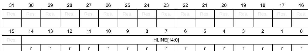
| 31 | 30 | 29 | 28 | 27 | 26 | 25 | 24 | 23 | 22 | 21 | 20 | 19 | 18 | 17 | 16 |
| Res. | Res. | Res. | Res. | Res. | Res. | Res. | Res. | Res. | Res. | Res. | Res. | Res. | Res. | Res. | Res. |
| 15 | 14 | 13 | 12 | 11 | 10 | 9 | 8 | 7 | 6 | 5 | 4 | 3 | 2 | 1 | 0 |
| Res. | HLINE[14:0] | ||||||||||||||
| r | r | r | r | r | r | r | r | r | r | r | r | r | r | r | |
Bits 31:15 Reserved, must be kept at reset value.
Bits 14:0 HLINE[14:0] : Horizontal line duration
This field returns the current total of the horizontal line period (HSA + HBP + HACT + HFP) counted in lane byte clock cycles.
44.15.59 DSI Host video VSA current configuration register (DSI_VVSACCR)
Address offset: 0x0154
Reset value: 0x0000 0000
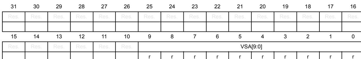
| 31 | 30 | 29 | 28 | 27 | 26 | 25 | 24 | 23 | 22 | 21 | 20 | 19 | 18 | 17 | 16 |
| Res. | Res. | Res. | Res. | Res. | Res. | Res. | Res. | Res. | Res. | Res. | Res. | Res. | Res. | Res. | Res. |
| 15 | 14 | 13 | 12 | 11 | 10 | 9 | 8 | 7 | 6 | 5 | 4 | 3 | 2 | 1 | 0 |
| Res. | Res. | Res. | Res. | Res. | Res. | VSA[9:0] | |||||||||
| r | r | r | r | r | r | r | r | r | r | ||||||
Bits 31:10 Reserved, must be kept at reset value.
Bits 9:0 VSA[9:0] : Vertical synchronism active duration
This field returns the current vertical synchronism active period measured in number of horizontal lines.
44.15.60 DSI Host video VBP current configuration register (DSI_VVBPCCR)
Address offset: 0x0158
Reset value: 0x0000 0000
| 31 | 30 | 29 | 28 | 27 | 26 | 25 | 24 | 23 | 22 | 21 | 20 | 19 | 18 | 17 | 16 |
|---|---|---|---|---|---|---|---|---|---|---|---|---|---|---|---|
| Res. | Res. | Res. | Res. | Res. | Res. | Res. | Res. | Res. | Res. | Res. | Res. | Res. | Res. | Res. | Res. |
| 15 | 14 | 13 | 12 | 11 | 10 | 9 | 8 | 7 | 6 | 5 | 4 | 3 | 2 | 1 | 0 |
| Res. | Res. | Res. | Res. | Res. | Res. | ||||||||||
| VBP[9:0] | |||||||||||||||
| r | r | r | r | r | r | r | r | r | r | ||||||
Bits 31:10 Reserved, must be kept at reset value.
Bits 9:0 VBP[9:0] : Vertical back-porch duration
This field returns the current vertical back-porch period measured in number of horizontal lines.
44.15.61 DSI Host video VFP current configuration register (DSI_VVFPCCR)
Address offset: 0x015C
Reset value: 0x0000 0000
| 31 | 30 | 29 | 28 | 27 | 26 | 25 | 24 | 23 | 22 | 21 | 20 | 19 | 18 | 17 | 16 |
|---|---|---|---|---|---|---|---|---|---|---|---|---|---|---|---|
| Res. | Res. | Res. | Res. | Res. | Res. | Res. | Res. | Res. | Res. | Res. | Res. | Res. | Res. | Res. | Res. |
| 15 | 14 | 13 | 12 | 11 | 10 | 9 | 8 | 7 | 6 | 5 | 4 | 3 | 2 | 1 | 0 |
| Res. | Res. | Res. | Res. | Res. | Res. | ||||||||||
| VFP[9:0] | |||||||||||||||
| r | r | r | r | r | r | r | r | r | r | ||||||
Bits 31:10 Reserved, must be kept at reset value.
Bits 9:0 VFP[9:0] : Vertical front-porch duration
This field returns the current vertical front-porch period measured in number of horizontal lines.
44.15.62 DSI Host video VA current configuration register (DSI_VVACCR)
Address offset: 0x0160
Reset value: 0x0000 0000
| 31 | 30 | 29 | 28 | 27 | 26 | 25 | 24 | 23 | 22 | 21 | 20 | 19 | 18 | 17 | 16 |
|---|---|---|---|---|---|---|---|---|---|---|---|---|---|---|---|
| Res. | Res. | Res. | Res. | Res. | Res. | Res. | Res. | Res. | Res. | Res. | Res. | Res. | Res. | Res. | Res. |
| 15 | 14 | 13 | 12 | 11 | 10 | 9 | 8 | 7 | 6 | 5 | 4 | 3 | 2 | 1 | 0 |
| Res. | Res. | ||||||||||||||
| VA[13:0] | |||||||||||||||
| r | r | r | r | r | r | r | r | r | r | r | r | r | r | ||
Bits 31:14 Reserved, must be kept at reset value.
Bits 13:0 VA[13:0] : Vertical active duration
This field returns the current vertical active period measured in number of horizontal lines.
44.15.63 DSI Host FIFO and buffer status register (DSI_FBSR)
Address offset: 0x0168
Reset value: 0x0005 0015
| 31 | 30 | 29 | 28 | 27 | 26 | 25 | 24 | 23 | 22 | 21 | 20 | 19 | 18 | 17 | 16 |
|---|---|---|---|---|---|---|---|---|---|---|---|---|---|---|---|
| Res. | Res. | Res. | Res. | Res. | Res. | Res. | Res. | APBF | APBE | ACBF | ACBE | Res. | Res. | VPBF | VPBE |
| r | r | r | r | r | r | ||||||||||
| 15 | 14 | 13 | 12 | 11 | 10 | 9 | 8 | 7 | 6 | 5 | 4 | 3 | 2 | 1 | 0 |
| Res. | Res. | Res. | Res. | Res. | Res. | Res. | Res. | APWFF | APWFE | ACWFF | ACWFE | VPWFF | VPWFE | VCWFF | VCWFE |
| r | r | r | r | r | r | r | r |
Bits 31:24 Reserved, must be kept at reset value.
Bit 23 APBF : Adapted command mode payload buffer full
This bit indicates the full status of the adapted command mode payload internal buffer:
0: Payload internal buffer not full
1: Payload internal buffer full
Bit 22 APBE : Adapted command mode payload buffer empty
This bit indicates the empty status of the adapted command mode payload internal buffer:
0: Payload internal buffer not empty
1: Payload internal buffer empty
Bit 21 ACBF : Adapted command mode command buffer full
This bit indicates the full status of the adapted command mode command internal buffer:
0: Command internal buffer not full
1: Command internal buffer full
Bit 20 ACBE : Adapted command mode command buffer empty
This bit indicates the empty status of the adapted command mode command internal buffer:
0: Command internal buffer not empty
1: Command internal buffer empty
Bits 19:18 Reserved, must be kept at reset value.
Bit 17 VPBF : Video mode payload buffer full
This bit indicates the full status of the video mode payload internal buffer:
0: Payload internal buffer not full
1: Payload internal buffer full
Bit 16 VPBE : Video mode payload buffer empty
This bit indicates the empty status of the video mode payload internal buffer:
0: Payload internal buffer not empty
1: Payload internal buffer empty
Bits 15:8 Reserved, must be kept at reset value.
Bit 7 APWFF : Adapted command mode payload write FIFO full
This bit indicates the full status of the adapted command mode write payload FIFO:
0: Write payload FIFO not full
1: Write payload FIFO full
Bit 6 APWFE : Adapted command mode payload write FIFO empty
This bit indicates the empty status of the adapted command mode write payload FIFO:
0: Write payload FIFO not empty
1: Write payload FIFO empty
Bit 5 ACWFF : Adapted command mode command write FIFO full
This bit indicates the full status of the adapted command mode write command FIFO:
0: Write command FIFO not full
1: Write command FIFO full
Bit 4 ACWFE : Adapted command mode command write FIFO empty
This bit indicates the empty status of the adapted command mode write command FIFO:
0: Write command FIFO not empty
1: Write command FIFO empty
Bit 3 VPWFF : Video mode payload write FIFO full
This bit indicates the full status of the video mode write payload FIFO:
0: Write payload FIFO not full
1: Write payload FIFO full
Bit 2 VPWFE : Video mode payload write FIFO empty
This bit indicates the empty status of the video mode write payload FIFO:
0: Write payload FIFO not empty
1: Write payload FIFO empty
Bit 1 VCWFF : Video mode command write FIFO full
This bit indicates the full status of the video mode write command FIFO:
0: Write command FIFO not full
1: Write command FIFO full
Bit 0 VCWFE : Video mode command write FIFO empty
This bit indicates the empty status of the video mode write command FIFO:
0: Write command FIFO not empty
1: Write command FIFO empty
44.16 DSI Wrapper registers
44.16.1 DSI Wrapper configuration register (DSI_WCFGR)
Address offset: 0x0400
Reset value: 0x0000 0000
| 31 | 30 | 29 | 28 | 27 | 26 | 25 | 24 | 23 | 22 | 21 | 20 | 19 | 18 | 17 | 16 |
|---|---|---|---|---|---|---|---|---|---|---|---|---|---|---|---|
| Res. | Res. | Res. | Res. | Res. | Res. | Res. | Res. | Res. | Res. | Res. | Res. | Res. | Res. | Res. | Res. |
| 15 | 14 | 13 | 12 | 11 | 10 | 9 | 8 | 7 | 6 | 5 | 4 | 3 | 2 | 1 | 0 |
| Res. | Res. | Res. | Res. | Res. | Res. | Res. | Res. | VSPOL | AR | TEPOL | TESRC | COLMUX[2:0] | DSIM | ||
| rw | rw | rw | rw | rw | rw | rw | rw | ||||||||
Bits 31:8 Reserved, must be kept at reset value.
Bit 7 VSPOL : VSync polarity
This bit selects the VSync edge on which the LTDC is halted. It can be changed only when DSI is stopped (DSI_WCR.DSIEN = 0 and DSI_CR.EN = 0). It is recommended to keep the default polarity configuration to guarantee a correct behavior.
0: LTDC halted on a falling edge
1: LTDC halted on a rising edge
Bit 6 AR : Automatic refresh
This bit selects the refresh mode in DBI mode. It can be changed only when DSI Host is stopped (DSI_CR.EN = 0).
0: automatic refresh mode disabled
1: automatic refresh mode enabled
Bit 5 TEPOL : TE polarity
This bit selects the polarity of the external pin tearing effect (TE) source. It can be changed only when DSI Host is stopped (DSI_CR.EN = 0).
0: rising edge
1: falling edge
Bit 4 TESRC : TE source
This bit selects the tearing effect (TE) source. It can be changed when DSI Host is stopped (DSI_CR.EN = 0).
0: DSI link
1: External pin
Bits 3:1 COLMUX[2:0] : Color multiplexing
This bitfield selects the color multiplexing used by DSI Host. It can be changed only when DSI Host is stopped (DSI_WCR.DSIEN = 0 and DSI_CR.EN = 0).
000: 16-bit configuration 1
001: 16-bit configuration 2
010: 16-bit configuration 3
011: 18-bit configuration 1
100: 18-bit configuration 2
101: 24-bit
Bit 0 DSIM : DSI mode
This bit selects the mode for the video transmission. It can be changed when DSI Host is stopped (DSI_CR.EN = 0).
0: Video mode
1: Adapted command mode
44.16.2 DSI Wrapper control register (DSI_WCR)
Address offset: 0x0404
Reset value: 0x0000 0000
| 31 | 30 | 29 | 28 | 27 | 26 | 25 | 24 | 23 | 22 | 21 | 20 | 19 | 18 | 17 | 16 |
|---|---|---|---|---|---|---|---|---|---|---|---|---|---|---|---|
| Res. | Res. | Res. | Res. | Res. | Res. | Res. | Res. | Res. | Res. | Res. | Res. | Res. | Res. | Res. | Res. |
| 15 | 14 | 13 | 12 | 11 | 10 | 9 | 8 | 7 | 6 | 5 | 4 | 3 | 2 | 1 | 0 |
| Res. | Res. | Res. | Res. | Res. | Res. | Res. | Res. | Res. | Res. | Res. | Res. | DSIEN | LTDCEN | SHTDN | COLM |
| rw | rs | rw | rw |
Bits 31:4 Reserved, must be kept at reset value.
Bit 3 DSIEN : DSI enable
This bit enables the DSI Wrapper.
0: DSI disabled
1: DSI enabled
Bit 2 LTDCEN : LTDC enable
This bit enables the LTDC for a frame transfer in adapted command mode.
0: LTDC disabled
1: LTDC enabled
Bit 1 SHTDN : Shutdown
This bit controls the display shutdown in video mode.
0: Display ON
1: Display OFF
Bit 0 COLM : Color mode
This bit controls the display color mode in video mode.
0: Full color mode
1: Eight color mode
44.16.3 DSI Wrapper interrupt enable register (DSI_WIER)
Address offset: 0x0408
Reset value: 0x0000 0000
| 31 | 30 | 29 | 28 | 27 | 26 | 25 | 24 | 23 | 22 | 21 | 20 | 19 | 18 | 17 | 16 |
|---|---|---|---|---|---|---|---|---|---|---|---|---|---|---|---|
| Res. | Res. | Res. | Res. | Res. | Res. | Res. | Res. | Res. | Res. | Res. | Res. | Res. | Res. | Res. | Res. |
| 15 | 14 | 13 | 12 | 11 | 10 | 9 | 8 | 7 | 6 | 5 | 4 | 3 | 2 | 1 | 0 |
| Res. | Res. | Res. | Res. | Res. | PLLUIE | PLLLIE | Res. | Res. | Res. | Res. | Res. | Res. | Res. | ERIE | TEIE |
| rw | rw | rw | rw |
- Bits 31:11 Reserved, must be kept at reset value.
- Bit 10
PLLUIE
: PLL unlock interrupt enable
- This bit enables the PLL unlock interrupt.
- 0: PLL unlock interrupt disabled
- 1: PLL unlock interrupt enabled
- Bit 9
PLLIE
: PLL lock interrupt enable
- This bit enables the PLL lock interrupt.
- 0: PLL lock interrupt disabled
- 1: PLL lock interrupt enabled
- Bits 8:2 Reserved, must be kept at reset value.
- Bit 1
ERIE
: End of refresh interrupt enable
- This bit enables the end of refresh interrupt.
- 0: End of refresh interrupt disabled
- 1: End of refresh interrupt enabled
- Bit 0
TEIE
: Tearing effect interrupt enable
- This bit enables the tearing effect interrupt.
- 0: Tearing effect interrupt disabled
- 1: Tearing effect interrupt enabled
44.16.4 DSI Wrapper interrupt and status register (DSI_WISR)
Address offset: 0x040C
Reset value: 0x0000 0000
| 31 | 30 | 29 | 28 | 27 | 26 | 25 | 24 | 23 | 22 | 21 | 20 | 19 | 18 | 17 | 16 |
|---|---|---|---|---|---|---|---|---|---|---|---|---|---|---|---|
| Res. | Res. | Res. | Res. | Res. | Res. | Res. | Res. | Res. | Res. | Res. | Res. | Res. | Res. | Res. | Res. |
| 15 | 14 | 13 | 12 | 11 | 10 | 9 | 8 | 7 | 6 | 5 | 4 | 3 | 2 | 1 | 0 |
| Res. | Res. | Res. | Res. | Res. | PLLUIF | PLLIF | PLLS | Res. | Res. | Res. | Res. | Res. | BUSY | ERIF | TEIF |
| r | r | r | r | r | r |
- Bits 31:11 Reserved, must be kept at reset value.
- Bit 10
PLLUIF
: PLL unlock interrupt flag
- This bit is set when the PLL becomes unlocked.
- 0: No PLL unlock event occurred
- 1: PLL unlock event occurred
- Bit 9
PLLIF
: PLL lock interrupt flag
- This bit is set when the PLL becomes locked.
- 0: No PLL lock event occurred
- 1: PLL lock event occurred
- Bit 8
PLLS
: PLL lock status
- This bit is set when the PLL is locked and cleared when it is unlocked.
- 0: PLL is unlocked.
- 1: PLL is locked.
- Bits 7:3 Reserved, must be kept at reset value.
Bit 2 BUSY : Busy flag
This bit is set when the transfer of a frame in adapted command mode is ongoing.
0: No transfer ongoing
1: Transfer ongoing
Bit 1 ERIF : End of refresh interrupt flag
This bit is set when the transfer of a frame in adapted command mode is finished.
0: No end of refresh event occurred
1: End of refresh event occurred
Bit 0 TEIF : Tearing effect interrupt flag
This bit is set when a tearing effect event occurs.
0: No tearing effect event occurred
1: Tearing effect event occurred
44.16.5 DSI Wrapper interrupt flag clear register (DSI_WIFCR)
Address offset: 0x0410
Reset value: 0x0000 0000
| 31 | 30 | 29 | 28 | 27 | 26 | 25 | 24 | 23 | 22 | 21 | 20 | 19 | 18 | 17 | 16 |
|---|---|---|---|---|---|---|---|---|---|---|---|---|---|---|---|
| Res. | Res. | Res. | Res. | Res. | Res. | Res. | Res. | Res. | Res. | Res. | Res. | Res. | Res. | Res. | Res. |
| 15 | 14 | 13 | 12 | 11 | 10 | 9 | 8 | 7 | 6 | 5 | 4 | 3 | 2 | 1 | 0 |
| Res. | Res. | Res. | Res. | Res. | CPLLUIF | CPLLIF | Res. | Res. | Res. | Res. | Res. | Res. | Res. | CERIF | CTEIF |
| w | w | w | w |
Bits 31:11 Reserved, must be kept at reset value.
Bit 10 CPLLUIF : Clear PLL unlock interrupt flag
Writing 1 clears the PLLUIF flag in the DSI_WSR register.
0: No effect
1: Clears the PLLUIF flag
Bit 9 CPLLIF : Clear PLL lock interrupt flag
Writing 1 clears the PLLIF flag in the DSI_WSR register.
0: No effect
1: Clears the PLLUIF flag
Bits 8:2 Reserved, must be kept at reset value.
Bit 1 CERIF : Clear end of refresh interrupt flag
Writing 1 clears the ERIF flag in the DSI_WSR register.
0: No effect
1: Clears the PLLUIF flag
Bit 0 CTEIF : Clear tearing effect interrupt flag
Writing 1 clears the TEIF flag in the DSI_WSR register.
0: No effect
1: Clears the PLLUIF flag
44.16.6 DSI Wrapper PHY configuration register 0 (DSI_WPCR0)
Address offset: 0x0418
Reset value: 0x0000 0000
| 31 | 30 | 29 | 28 | 27 | 26 | 25 | 24 | 23 | 22 | 21 | 20 | 19 | 18 | 17 | 16 |
|---|---|---|---|---|---|---|---|---|---|---|---|---|---|---|---|
| Res. | Res. | Res. | Res. | Res. | Res. | Res. | Res. | Res. | Res. | Res. | Res. | Res. | Res. | Res. | Res. |
| 15 | 14 | 13 | 12 | 11 | 10 | 9 | 8 | 7 | 6 | 5 | 4 | 3 | 2 | 1 | 0 |
| Res. | Res. | FTXSM DL | FTXSM CL | Res. | Res. | Res. | SWDL1 | SWDL0 | SWCL | Res. | Res. | Res. | Res. | Res. | Res. |
| rw | rw | rw | rw | rw |
Bits 31:14 Reserved, must be kept at reset value.
Bit 13 FTXSM DL : Force in TX Stop mode the data lanes
This bit forces the data lanes in TX stop mode. It is used to initialize a lane module in transmit mode. It causes the lane module to immediately jump to transmit control mode and to begin transmitting a stop state (LP-11). It can be used to go back in TX mode after a wrong BTA sequence.
0: No effect
1: Force the data lanes in TX Stop mode
Bit 12 FTXSM CL : Force in TX Stop mode the clock lane
This bit forces the clock lane in TX stop mode. It is used to initialize a lane module in transmit mode. It causes the lane module to immediately jump to transmit control mode and to begin transmitting a stop state (LP-11). It can be used to go back in TX mode after a wrong BTA sequence.
0: No effect
1: Force the clock lane in TX Stop mode
Bits 11:9 Reserved, must be kept at reset value.
Bit 8 SWDL 1 : Swap data lane 1 pins
This bit swaps the pins on clock lane.
0: Regular clock lane pin configuration
1: Swapped clock lane pin
Bit 7 SWDL 0 : Swap data lane 0 pins
This bit swaps the pins on data lane 0.
0: Regular clock lane pin configuration
1: Swapped clock lane pin
Bit 6 SWCL : Swap clock lane pins
This bit swaps the pins on clock lane.
0: Regular clock lane pin configuration
1: Swapped clock lane pin
Bits 5:0 Reserved, must be kept at reset value.
44.16.7 DSI Wrapper regulator and PLL control register (DSI_WRPCR)
Address offset: 0x0430
Reset value: 0x0000 0000
| 31 | 30 | 29 | 28 | 27 | 26 | 25 | 24 | 23 | 22 | 21 | 20 | 19 | 18 | 17 | 16 |
|---|---|---|---|---|---|---|---|---|---|---|---|---|---|---|---|
| Res. | BC[1:0] | ODF[8:0] | |||||||||||||
| rw | rw | rw | rw | rw | rw | rw | rw | rw | rw | rw | rw | rw | rw | rw | |
| 15 | 14 | 13 | 12 | 11 | 10 | 9 | 8 | 7 | 6 | 5 | 4 | 3 | 2 | 1 | 0 |
| IDF[4:0] | NDIV[8:0] | Res. | PLLEN | ||||||||||||
| rw | rw | rw | rw | rw | rw | rw | rw | rw | rw | rw | rw | rw | rw | rw | |
Bit 31 Reserved, must be kept at reset value.
Bits 30:29 BC[1:0] : Band control
This field selects the VCO frequency band.
00: 500 to 800 MHz
01: 800 to 1000 MHz
Others: Reserved
Bits 28:20 ODF[8:0] : PLL output division factor
This field configures the PLL output division factor.
0: PLL output divided by 1
1: PLL output divided by 1
2: PLL output divided by 2
...
511: PLL output divided by 511
Bits 19:11 IDF[8:0] : PLL input division factor
This field configures the PLL input division factor.
0: PLL input divided by 1
1: PLL input divided by 1
2: PLL input divided by 2
...
511: PLL input divided by 511
Bits 10:2 NDIV[8:0] : PLL loop division factor
This field configures the PLL loop division factor.
0: PLL loop divided by 1x2
1: PLL loop divided by 1x2
2: PLL loop divided by 2x2
...
511: PLL loop divided by 511x2
Bit 1 Reserved, must be kept at reset value.
Bit 0 PLLEN : PLL enable
This bit enables the D-PHY PLL.
0: PLL disabled
1: PLL enabled
44.16.8 DSI Wrapper PLL tuning register (DSI_WPTR)
Address offset: 0x0434
Reset value: 0x0000 0000
| 31 | 30 | 29 | 28 | 27 | 26 | 25 | 24 | 23 | 22 | 21 | 20 | 19 | 18 | 17 | 16 |
| Res. | Res. | Res. | Res. | Res. | Res. | Res. | Res. | Res. | Res. | Res. | Res. | Res. | Res. | Res. | Res. |
| 15 | 14 | 13 | 12 | 11 | 10 | 9 | 8 | 7 | 6 | 5 | 4 | 3 | 2 | 1 | 0 |
| LPF[3:0] | CP[3:0] | Res. | Res. | Res. | Res. | Res. | Res. | Res. | Res. | ||||||
| rw | rw | rw | rw | rw | rw | rw | rw | ||||||||
Bits 31:16 Reserved, must be kept at reset value.
Bits 15:12 LPF[3:0] : Loop filter
This field controls the PLL loop filter, it must be configured according to the PFD frequency range:
0000: 2.0 to 4.4 MHz
0001: 4.4 to 30.9 MHz
0010: 30.9 to 50 MHz
Others: Reserved
Bits 11:8 CP[3:0] : Charge pump
This field controls the PLL charge pump, it must be configured according to the PFD frequency range and the LPF value:
0000: 2.0 to 4.4 MHz and 14.1 to 30.9 MHz
0001: 4.4 to 14.1 MHz
0010: 45.7 to 50 MHz
0011: 30.9 to 45.7 MHz
Others: Reserved
Bits 7:0 Reserved, must be kept at reset value.
44.17 DSI bias registers
44.17.1 DSI bias configuration register (DSI_BCFGR)
Address offset: 0x0808
Reset value: 0x0000 0000
| 31 | 30 | 29 | 28 | 27 | 26 | 25 | 24 | 23 | 22 | 21 | 20 | 19 | 18 | 17 | 16 |
| Res. | Res. | Res. | Res. | Res. | Res. | Res. | Res. | Res. | Res. | Res. | Res. | Res. | Res. | Res. | Res. |
| 15 | 14 | 13 | 12 | 11 | 10 | 9 | 8 | 7 | 6 | 5 | 4 | 3 | 2 | 1 | 0 |
| Res. | Res. | Res. | Res. | Res. | Res. | Res. | Res. | Res. | PWRUP | Res. | Res. | Res. | Res. | Res. | Res. |
| rw | |||||||||||||||
Bits 31:7 Reserved, must be kept at reset value.
Bit 6 PWRUP : Power-up
This bit powers-up the reference bias for the MIPI D-PHY
0: Reference bias is powered down.
1: Reference bias is powered up.
Bits 5:0 Reserved, must be kept at reset value.
44.18 D-PHY registers
44.18.1 DSI D-PHY clock band control register (DSI_DPCBCR)
Address offset: 0x0C04
Reset value: 0x0000 0000
| 31 | 30 | 29 | 28 | 27 | 26 | 25 | 24 | 23 | 22 | 21 | 20 | 19 | 18 | 17 | 16 |
|---|---|---|---|---|---|---|---|---|---|---|---|---|---|---|---|
| Res. | Res. | Res. | Res. | Res. | Res. | Res. | Res. | Res. | Res. | Res. | Res. | Res. | Res. | Res. | Res. |
| 15 | 14 | 13 | 12 | 11 | 10 | 9 | 8 | 7 | 6 | 5 | 4 | 3 | 2 | 1 | 0 |
| Res. | Res. | Res. | Res. | Res. | Res. | Res. | Res. | BC[4:0] | Res. | Res. | Res. | ||||
| rw | rw | rw | rw | rw | |||||||||||
Bits 31:8 Reserved, must be kept at reset value.
Bits 7:3 BC[4:0] : Band control
This field selects the frequency band used by the D-PHY.
00000: 80 to 100 MHz
00001: 100 to 120 MHz
00010: 120 to 160 MHz
00011: 160 to 200 MHz
00100: 200 to 240 MHz
00101: 240 to 320 MHz
00110: 320 to 390 MHz
00111: 390 to 450 MHz
01000: 450 to 510 MHz
Others: Reserved
Bits 2:0 Reserved, must be kept at reset value.
44.18.2 DSI D-PHY clock skew rate control register (DSI_DPCSRCR)
Address offset: 0x0C34
Reset value: 0x0000 0000
| 31 | 30 | 29 | 28 | 27 | 26 | 25 | 24 | 23 | 22 | 21 | 20 | 19 | 18 | 17 | 16 |
|---|---|---|---|---|---|---|---|---|---|---|---|---|---|---|---|
| Res. | Res. | Res. | Res. | Res. | Res. | Res. | Res. | Res. | Res. | Res. | Res. | Res. | Res. | Res. | Res. |
| 15 | 14 | 13 | 12 | 11 | 10 | 9 | 8 | 7 | 6 | 5 | 4 | 3 | 2 | 1 | 0 |
| Res. | Res. | Res. | Res. | Res. | Res. | Res. | Res. | SRC[7:0] | |||||||
| rw | rw | rw | rw | rw | rw | rw | rw | ||||||||
Bits 31:8 Reserved, must be kept at reset value.
Bits 7:0 SRC[7:0] : Slew rate control
This field selects the slew rate for HS-TX speed.
0x0E: 80 to 750 Mbit/s
Others: Reserved
44.18.3 DSI D-PHY data lane 0 HS offset control register (DSI_DPDL0HSOCR)
Address offset: 0x0C5C
Reset value: 0x0000 0000
| 31 | 30 | 29 | 28 | 27 | 26 | 25 | 24 | 23 | 22 | 21 | 20 | 19 | 18 | 17 | 16 |
|---|---|---|---|---|---|---|---|---|---|---|---|---|---|---|---|
| Res. | Res. | Res. | Res. | Res. | Res. | Res. | Res. | Res. | Res. | Res. | Res. | Res. | Res. | Res. | Res. |
| 15 | 14 | 13 | 12 | 11 | 10 | 9 | 8 | 7 | 6 | 5 | 4 | 3 | 2 | 1 | 0 |
| Res. | Res. | Res. | Res. | Res. | Res. | Res. | Res. | HSPRPO[3:0] | Res. | Res. | Res. | Res. | |||
| rw | rw | rw | rw | ||||||||||||
Bits 31:8 Reserved, must be kept at reset value.
Bits 7:4 HSPRPO[3:0] : HS prepare offset
This field selects the offset in lane byte clock to be added to the HS prepare timing. The offset is dependent on the frequency band selected for the D-PHY
0000: 100 to 120 MHz - 120 to 160 MHz - 240 to 320 MHz
0001: 80 to 100 MHz - 160 to 200 MHz - 200 to 240 MHz - 320 to 390 MHz
0010: 390 to 450 MHz - 450 to 510 MHz
Others: Reserved
Bits 3:0 Reserved, must be kept at reset value.
44.18.4 DSI D-PHY data lane 0 HS LPX offset control register (DSI_DPDL0LPXOCR)
Address offset: 0x0C60
Reset value: 0x0000 0000
| 31 | 30 | 29 | 28 | 27 | 26 | 25 | 24 | 23 | 22 | 21 | 20 | 19 | 18 | 17 | 16 |
|---|---|---|---|---|---|---|---|---|---|---|---|---|---|---|---|
| Res. | Res. | Res. | Res. | Res. | Res. | Res. | Res. | Res. | Res. | Res. | Res. | Res. | Res. | Res. | Res. |
| 15 | 14 | 13 | 12 | 11 | 10 | 9 | 8 | 7 | 6 | 5 | 4 | 3 | 2 | 1 | 0 |
| Res. | Res. | Res. | Res. | Res. | Res. | Res. | Res. | Res. | Res. | Res. | Res. | LPXO[3:0] | |||
| rw | rw | rw | rw | ||||||||||||
Bits 31:4 Reserved, must be kept at reset value.
Bits 3:0 LPXO[3:0] : LPX offset
This field selects the offset added to fine tune the delay associated to the following states: INIT_STATE, STOP_STATE, LP01_STATE and LP11_STATE.
This field is a 4-bit signed value in complement 2 format (-8 to +7 range).
The LPX timing is composed of a unsigned fixed 7-bit value dependent of the frequency band selected for the D-PHY and the 4-bit signed value of this field.
The LPX timing is expressed in lane byte clock period.
The LPX fixed value is:
80 to 120 MHz: 7'h01
120 to 160 MHz: 7'h02
160 to 320 MHz: 7'h03
320 to 450 MHz: 7'h04
450 to 510 MHz: 7'h05
As the resulting LPX timing is an unsigned 7-bit value, the user must take care of underflow when the value is negative (complement 2 format).
44.18.5 DSI D-PHY data lane 0 band control register (DSI_DPDLOBCR)
Address offset: 0x0C70
Reset value: 0x0000 0000
| 31 | 30 | 29 | 28 | 27 | 26 | 25 | 24 | 23 | 22 | 21 | 20 | 19 | 18 | 17 | 16 |
|---|---|---|---|---|---|---|---|---|---|---|---|---|---|---|---|
| Res. | Res. | Res. | Res. | Res. | Res. | Res. | Res. | Res. | Res. | Res. | Res. | Res. | Res. | Res. | Res. |
| 15 | 14 | 13 | 12 | 11 | 10 | 9 | 8 | 7 | 6 | 5 | 4 | 3 | 2 | 1 | 0 |
| Res. | Res. | Res. | Res. | Res. | Res. | Res. | Res. | Res. | Res. | Res. | BC[4:0] | ||||
| rw | rw | rw | rw | rw | |||||||||||
Bits 31:5 Reserved, must be kept at reset value.
Bits 4:0 BC[4:0] : Band control
This field selects the frequency band used by the D-PHY.
00000: 80 to 100 MHz
00001: 100 to 120 MHz
00010: 120 to 160 MHz
00011: 160 to 200 MHz
00100: 200 to 240 MHz
00101: 240 to 320 MHz
00110: 320 to 390 MHz
00111: 390 to 450 MHz
01000: 450 to 510 MHz
Others: Reserved
44.18.6 DSI D-PHY data lane 0 skew rate control register (DSI_DPDLOSRCR)
Address offset: 0x0CA0
Reset value: 0x0000 0000
| 31 | 30 | 29 | 28 | 27 | 26 | 25 | 24 | 23 | 22 | 21 | 20 | 19 | 18 | 17 | 16 |
|---|---|---|---|---|---|---|---|---|---|---|---|---|---|---|---|
| Res. | Res. | Res. | Res. | Res. | Res. | Res. | Res. | Res. | Res. | Res. | Res. | Res. | Res. | Res. | Res. |
| 15 | 14 | 13 | 12 | 11 | 10 | 9 | 8 | 7 | 6 | 5 | 4 | 3 | 2 | 1 | 0 |
| Res. | Res. | Res. | Res. | Res. | Res. | Res. | Res. | SRC[7:0] | |||||||
| rw | rw | rw | rw | rw | rw | rw | rw | ||||||||
Bits 31:8 Reserved, must be kept at reset value.
Bits 7:0 SRC[7:0] : Slew rate control
This field selects the slew rate for HS-TX speed.
0x0E: 80 to 750 Mbit/s
Others: Reserved
44.18.7 DSI D-PHY data lane 1 HS offset control register (DSI_DPD1HSOCR)
Address offset: 0x0CF4
Reset value: 0x0000 0000
| 31 | 30 | 29 | 28 | 27 | 26 | 25 | 24 | 23 | 22 | 21 | 20 | 19 | 18 | 17 | 16 |
|---|---|---|---|---|---|---|---|---|---|---|---|---|---|---|---|
| Res. | Res. | Res. | Res. | Res. | Res. | Res. | Res. | Res. | Res. | Res. | Res. | Res. | Res. | Res. | Res. |
| 15 | 14 | 13 | 12 | 11 | 10 | 9 | 8 | 7 | 6 | 5 | 4 | 3 | 2 | 1 | 0 |
| Res. | Res. | Res. | Res. | Res. | Res. | Res. | Res. | HSPRPO[3:0] | Res. | Res. | Res. | Res. | |||
| rw | rw | rw | rw | ||||||||||||
Bits 31:8 Reserved, must be kept at reset value.
Bits 7:4 HSPRPO[3:0] : HS prepare offset
This field selects the offset in lane byte clock to be added to the HS prepare timing. The offset is dependent on the frequency band selected for the D-PHY
0000: 100 to 120 MHz - 120 to 160 MHz - 240 to 320 MHz
0001: 80 to 100 MHz - 160 to 200 MHz - 200 to 240 MHz - 320 to 390 MHz
0010: 390 to 450 MHz - 450 to 510 MHz
Others: Reserved
Bits 3:0 Reserved, must be kept at reset value.
44.18.8 DSI D-PHY data lane 1 HS LPX offset control register (DSI_DPDL1LPXOCR)
Address offset: 0x0CF8
Reset value: 0x0000 0000
| 31 | 30 | 29 | 28 | 27 | 26 | 25 | 24 | 23 | 22 | 21 | 20 | 19 | 18 | 17 | 16 |
|---|---|---|---|---|---|---|---|---|---|---|---|---|---|---|---|
| Res. | Res. | Res. | Res. | Res. | Res. | Res. | Res. | Res. | Res. | Res. | Res. | Res. | Res. | Res. | Res. |
| 15 | 14 | 13 | 12 | 11 | 10 | 9 | 8 | 7 | 6 | 5 | 4 | 3 | 2 | 1 | 0 |
| Res. | Res. | Res. | Res. | Res. | Res. | Res. | Res. | Res. | Res. | Res. | Res. | LPXO[3:0] | |||
| rw | rw | rw | rw | ||||||||||||
Bits 31:4 Reserved, must be kept at reset value.
Bits 3:0 LPXO[3:0] : LPX offset
This field selects the offset added to fine tune the delay associated to the following states: INIT_STATE, STOP_STATE, LP01_STATE and LP11_STATE.
This field is a 4-bit signed value in complement 2 format.
The LPX timing is composed of a unsigned fixed 7-bit value dependent of the frequency band selected for the D-PHY and the 4-bit signed value of this field.
The offset is expressed in lane byte clock period.
As the resulting LPX timing is an unsigned 7-bit value, the user must take care of underflow when the value is negative (complement 2 format).
44.18.9 DSI D-PHY data lane 1 band control register (DSI_DPDL1BCR)
Address offset: 0x0D08
Reset value: 0x0000 0000
| 31 | 30 | 29 | 28 | 27 | 26 | 25 | 24 | 23 | 22 | 21 | 20 | 19 | 18 | 17 | 16 |
|---|---|---|---|---|---|---|---|---|---|---|---|---|---|---|---|
| Res. | Res. | Res. | Res. | Res. | Res. | Res. | Res. | Res. | Res. | Res. | Res. | Res. | Res. | Res. | Res. |
| 15 | 14 | 13 | 12 | 11 | 10 | 9 | 8 | 7 | 6 | 5 | 4 | 3 | 2 | 1 | 0 |
| Res. | Res. | Res. | Res. | Res. | Res. | Res. | Res. | Res. | Res. | Res. | BC[4:0] | ||||
| rw | rw | rw | rw | rw | |||||||||||
Bits 31:5 Reserved, must be kept at reset value.
Bits 4:0 BC[4:0] : Band control
This field selects the frequency band used by the D-PHY.
00000: 80 to 100 MHz
00001: 100 to 120 MHz
00010: 120 to 160 MHz
00011: 160 to 200 MHz
00100: 200 to 240 MHz
00101: 240 to 320 MHz
00110: 320 to 390 MHz
00111: 390 to 450 MHz
01000: 450 to 510 MHz
Others: Reserved
44.18.10 DSI D-PHY data lane 1 skew rate control register(DSI_DPDL1SRCR)
Address offset: 0x0D38
Reset value: 0x0000 0000
| 31 | 30 | 29 | 28 | 27 | 26 | 25 | 24 | 23 | 22 | 21 | 20 | 19 | 18 | 17 | 16 |
|---|---|---|---|---|---|---|---|---|---|---|---|---|---|---|---|
| Res. | Res. | Res. | Res. | Res. | Res. | Res. | Res. | Res. | Res. | Res. | Res. | Res. | Res. | Res. | Res. |
| 15 | 14 | 13 | 12 | 11 | 10 | 9 | 8 | 7 | 6 | 5 | 4 | 3 | 2 | 1 | 0 |
| Res. | Res. | Res. | Res. | Res. | Res. | Res. | Res. | SRC[7:0] | |||||||
| rw | rw | rw | rw | rw | rw | rw | rw | ||||||||
Bits 31:8 Reserved, must be kept at reset value.
Bits 7:0 SRC[7:0] : Slew rate controlThis field selects the slew rate for HS-TX speed.
0x0E: 80 to 750 Mbit/s
Others: Reserved
44.18.11 DSI register map
Table 447. DSI register map and reset values
| Offset | Register | 31 | 30 | 29 | 28 | 27 | 26 | 25 | 24 | 23 | 22 | 21 | 20 | 19 | 18 | 17 | 16 | 15 | 14 | 13 | 12 | 11 | 10 | 9 | 8 | 7 | 6 | 5 | 4 | 3 | 2 | 1 | 0 |
|---|---|---|---|---|---|---|---|---|---|---|---|---|---|---|---|---|---|---|---|---|---|---|---|---|---|---|---|---|---|---|---|---|---|
| 0x0000 | DSI_VR | VERSION[31:0] | |||||||||||||||||||||||||||||||
| Reset value | 0 | 0 | 1 | 1 | 0 | 0 | 0 | 1 | 0 | 0 | 1 | 1 | 0 | 1 | 0 | 0 | 0 | 0 | 1 | 1 | 0 | 0 | 0 | 1 | 0 | 0 | 1 | 0 | 1 | 1 | 0 | 0 | |
| 0x0004 | DSI_CR | Res. | Res. | Res. | Res. | Res. | Res. | Res. | Res. | Res. | Res. | Res. | Res. | Res. | Res. | Res. | Res. | Res. | Res. | Res. | Res. | Res. | Res. | Res. | Res. | Res. | Res. | Res. | Res. | Res. | Res. | Res. | EN |
| Reset value | 0 | ||||||||||||||||||||||||||||||||
| 0x0008 | DSI_CCR | Res. | Res. | Res. | Res. | Res. | Res. | Res. | Res. | Res. | Res. | Res. | Res. | Res. | Res. | Res. | Res. | TOCKDIV[7:0] | TXECKDIV[7:0] | ||||||||||||||
| Reset value | 0 | 0 | 0 | 0 | 0 | 0 | 0 | 0 | 0 | 0 | 0 | 0 | 0 | 0 | 0 | 0 | |||||||||||||||||
| 0x000C | DSI_LVCIDR | Res. | Res. | Res. | Res. | Res. | Res. | Res. | Res. | Res. | Res. | Res. | Res. | Res. | Res. | Res. | Res. | Res. | Res. | Res. | Res. | Res. | Res. | Res. | Res. | Res. | Res. | Res. | Res. | Res. | Res. | VCID [1:0] | |
| Reset value | 0 | 0 | |||||||||||||||||||||||||||||||
| 0x0010 | DSI_LCOLCR | Res. | Res. | Res. | Res. | Res. | Res. | Res. | Res. | Res. | Res. | Res. | Res. | Res. | Res. | Res. | Res. | Res. | Res. | Res. | Res. | Res. | Res. | Res. | LPE | Res. | Res. | Res. | Res. | COLC[3:0] | |||
| Reset value | 0 | 0 | 0 | 0 | 0 | ||||||||||||||||||||||||||||
| 0x0014 | DSI_LPCR | Res. | Res. | Res. | Res. | Res. | Res. | Res. | Res. | Res. | Res. | Res. | Res. | Res. | Res. | Res. | Res. | Res. | Res. | Res. | Res. | Res. | Res. | Res. | Res. | Res. | Res. | Res. | Res. | Res. | HSP | VSP | DEP |
| Reset value | 0 | 0 | 0 | ||||||||||||||||||||||||||||||
| 0x0018 | DSI_LPMCR | Res. | Res. | Res. | Res. | Res. | Res. | Res. | Res. | LPSIZE[7:0] | Res. | Res. | Res. | Res. | Res. | Res. | Res. | Res. | VLPSIZE[7:0] | ||||||||||||||
| Reset value | 0 | 0 | 0 | 0 | 0 | 0 | 0 | 0 | 0 | 0 | 0 | 0 | 0 | 0 | 0 | 0 | |||||||||||||||||
| 0x001C- 0x0028 | Reserved | Reserved | |||||||||||||||||||||||||||||||
| 0x002C | DSI_PCR | Res. | Res. | Res. | Res. | Res. | Res. | Res. | Res. | Res. | Res. | Res. | Res. | Res. | Res. | Res. | Res. | Res. | Res. | Res. | Res. | Res. | Res. | Res. | Res. | Res. | ETTX LPE | CRCRXE | ECCRXE | BTAE | ETRXE | ETTXE | Res. |
| Reset value | 0 | 0 | 0 | 0 | 0 | 0 | |||||||||||||||||||||||||||
| 0x0030 | DSI_GVCDR | Res. | Res. | Res. | Res. | Res. | Res. | Res. | Res. | Res. | Res. | Res. | Res. | Res. | Res. | VCIDTX [1:0] | Res. | Res. | Res. | Res. | Res. | Res. | Res. | Res. | Res. | Res. | Res. | Res. | Res. | Res. | VCIDRX [1:0] | ||
| Reset value | 0 | 0 | 0 | 0 | |||||||||||||||||||||||||||||
| 0x0034 | DSI_MCR | Res. | Res. | Res. | Res. | Res. | Res. | Res. | Res. | Res. | Res. | Res. | Res. | Res. | Res. | Res. | Res. | Res. | Res. | Res. | Res. | Res. | Res. | Res. | Res. | Res. | Res. | Res. | Res. | Res. | Res. | Res. | CMDM |
| Reset value | 1 | ||||||||||||||||||||||||||||||||
| 0x0038 | DSI_VMCR | Res. | Res. | Res. | Res. | Res. | Res. | PGO | Res. | Res. | Res. | PGM | Res. | Res. | Res. | PGE | LPCE | FBTAAE | LPHPPE | LPHBPE | LVAE | LPVFPE | LPVBPE | LPVSAE | Res. | Res. | Res. | Res. | Res. | Res. | Res. | VMT [1:0] | |
| Reset value | 0 | 0 | 0 | 0 | 0 | 0 | 0 | 0 | 0 | 0 | 0 | 0 | 0 | ||||||||||||||||||||
| 0x003C | DSI_VPCR | Res. | Res. | Res. | Res. | Res. | Res. | Res. | Res. | Res. | Res. | Res. | Res. | Res. | Res. | VPSIZE[13:0] | Res. | Res. | Res. | Res. | |||||||||||||
| Reset value | 0 | 0 | 0 | 0 | 0 | 0 | 0 | 0 | 0 | 0 | 0 | 0 | 0 | 0 | |||||||||||||||||||
| 0x0040 | DSI_VCCR | Res. | Res. | Res. | Res. | Res. | Res. | Res. | Res. | Res. | Res. | Res. | Res. | Res. | Res. | Res. | Res. | Res. | Res. | Res. | NUMC[12:0] | ||||||||||||
| Reset value | 0 | 0 | 0 | 0 | 0 | 0 | 0 | 0 | 0 | 0 | 0 | 0 | 0 | ||||||||||||||||||||
| 0x0044 | DSI_VNPCR | Res. | Res. | Res. | Res. | Res. | Res. | Res. | Res. | Res. | Res. | Res. | Res. | Res. | Res. | Res. | Res. | Res. | Res. | Res. | NPSIZE[12:0] | ||||||||||||
| Reset value | 0 | 0 | 0 | 0 | 0 | 0 | 0 | 0 | 0 | 0 | 0 | 0 | 0 | ||||||||||||||||||||
| 0x0048 | DSI_VHSACR | Res. | Res. | Res. | Res. | Res. | Res. | Res. | Res. | Res. | Res. | Res. | Res. | Res. | Res. | Res. | Res. | Res. | Res. | Res. | Res. | HSA[11:0] | |||||||||||
| Reset value | 0 | 0 | 0 | 0 | 0 | 0 | 0 | 0 | 0 | 0 | 0 | 0 | |||||||||||||||||||||
| 0x004C | DSI_VHBPCR | Res. | Res. | Res. | Res. | Res. | Res. | Res. | Res. | Res. | Res. | Res. | Res. | Res. | Res. | Res. | Res. | Res. | Res. | Res. | Res. | HBP[11:0] | |||||||||||
| Reset value | 0 | 0 | 0 | 0 | 0 | 0 | 0 | 0 | 0 | 0 | 0 | 0 | |||||||||||||||||||||
| 0x0050 | DSI_VLCR | Res. | Res. | Res. | Res. | Res. | Res. | Res. | Res. | Res. | Res. | Res. | Res. | Res. | Res. | Res. | Res. | Res. | HLINE[14:0] | ||||||||||||||
| Reset value | 0 | 0 | 0 | 0 | 0 | 0 | 0 | 0 | 0 | 0 | 0 | 0 | 0 | 0 | 0 | ||||||||||||||||||
Table 447. DSI register map and reset values (continued)
| Offset | Register | 31 | 30 | 29 | 28 | 27 | 26 | 25 | 24 | 23 | 22 | 21 | 20 | 19 | 18 | 17 | 16 | 15 | 14 | 13 | 12 | 11 | 10 | 9 | 8 | 7 | 6 | 5 | 4 | 3 | 2 | 1 | 0 |
|---|---|---|---|---|---|---|---|---|---|---|---|---|---|---|---|---|---|---|---|---|---|---|---|---|---|---|---|---|---|---|---|---|---|
| 0x0054 | DSI_VVSACR | Res. | Res. | Res. | Res. | Res. | Res. | Res. | Res. | Res. | Res. | Res. | Res. | Res. | Res. | Res. | Res. | Res. | Res. | Res. | Res. | Res. | Res. | VSA[9:0] | |||||||||
| Reset value | 0 | 0 | 0 | 0 | 0 | 0 | 0 | 0 | 0 | 0 | |||||||||||||||||||||||
| 0x0058 | DSI_VVBPCR | Res. | Res. | Res. | Res. | Res. | Res. | Res. | Res. | Res. | Res. | Res. | Res. | Res. | Res. | Res. | Res. | Res. | Res. | Res. | Res. | Res. | Res. | VBP[9:0] | |||||||||
| Reset value | 0 | 0 | 0 | 0 | 0 | 0 | 0 | 0 | 0 | 0 | |||||||||||||||||||||||
| 0x005C | DSI_VVFPCR | Res. | Res. | Res. | Res. | Res. | Res. | Res. | Res. | Res. | Res. | Res. | Res. | Res. | Res. | Res. | Res. | Res. | Res. | Res. | Res. | Res. | Res. | VFP[9:0] | |||||||||
| Reset value | 0 | 0 | 0 | 0 | 0 | 0 | 0 | 0 | 0 | 0 | |||||||||||||||||||||||
| 0x0060 | DSI_VVACR | Res. | Res. | Res. | Res. | Res. | Res. | Res. | Res. | Res. | Res. | Res. | Res. | Res. | Res. | Res. | Res. | Res. | Res. | VA[13:0] | |||||||||||||
| Reset value | 0 | 0 | 0 | 0 | 0 | 0 | 0 | 0 | 0 | 0 | 0 | 0 | 0 | 0 | |||||||||||||||||||
| 0x0064 | DSI_LCCR | Res. | Res. | Res. | Res. | Res. | Res. | Res. | Res. | Res. | Res. | Res. | Res. | Res. | Res. | Res. | Res. | CMDSIZE[15:0] | |||||||||||||||
| Reset value | 0 | 0 | 0 | 0 | 0 | 0 | 0 | 0 | 0 | 0 | 0 | 0 | 0 | 0 | 0 | 0 | |||||||||||||||||
| 0x0068 | DSI_CMCR | Res. | Res. | Res. | Res. | Res. | Res. | Res. | Res. | MRDPS | Res. | Res. | Res. | DLWTX | DSR0TX | DSW1TX | DSW0TX | Res. | GLWTX | GSR2TX | GSR1TX | GSR0TX | GSW2TX | GSW1TX | GSW0TX | Res. | Res. | Res. | Res. | Res. | Res. | ARE | TEARE |
| Reset value | 0 | 0 | 0 | 0 | 0 | 0 | 0 | 0 | 0 | 0 | 0 | 0 | 0 | 0 | |||||||||||||||||||
| 0x006C | DSI_GHCR | Res. | Res. | Res. | Res. | Res. | Res. | Res. | Res. | WCMSB[7:0] | WCLSB[7:0] | VCID[1:0] | DT[5:0] | ||||||||||||||||||||
| Reset value | 0 | 0 | 0 | 0 | 0 | 0 | 0 | 0 | 0 | 0 | 0 | 0 | 0 | 0 | 0 | 0 | 0 | 0 | 0 | 0 | 0 | 0 | 0 | 0 | |||||||||
| 0x0070 | DSI_GPDR | DATA4[7:0] | DATA3[7:0] | DATA2[7:0] | DATA1[7:0] | ||||||||||||||||||||||||||||
| Reset value | 0 | 0 | 0 | 0 | 0 | 0 | 0 | 0 | 0 | 0 | 0 | 0 | 0 | 0 | 0 | 0 | 0 | 0 | 0 | 0 | 0 | 0 | 0 | 0 | 0 | 0 | 0 | 0 | 0 | 0 | 0 | 0 | |
| 0x0074 | DSI_GPSR | Res. | Res. | Res. | Res. | Res. | Res. | Res. | Res. | Res. | Res. | Res. | Res. | PBF | PBE | CMDBF | CMDBEB | Res. | Res. | Res. | Res. | Res. | Res. | Res. | Res. | RCB | PRDFF | PRDFE | PWRFF | PWRFE | CMDFE | CMDFE | |
| Reset value | 0 | 1 | 0 | 1 | 0 | 0 | 1 | 0 | 1 | 0 | 1 | ||||||||||||||||||||||
| 0x0078 | DSI_TCCR0 | HSTX_TOCNT[15:0] | LPRX_TOCNT[15:0] | ||||||||||||||||||||||||||||||
| Reset value | 0 | 0 | 0 | 0 | 0 | 0 | 0 | 0 | 0 | 0 | 0 | 0 | 0 | 0 | 0 | 0 | 0 | 0 | 0 | 0 | 0 | 0 | 0 | 0 | 0 | 0 | 0 | 0 | 0 | 0 | 0 | 0 | |
| 0x007C | DSI_TCCR1 | Res. | Res. | Res. | Res. | Res. | Res. | Res. | Res. | Res. | Res. | Res. | Res. | Res. | Res. | Res. | Res. | HSRD_TOCNT[15:0] | |||||||||||||||
| Reset value | 0 | 0 | 0 | 0 | 0 | 0 | 0 | 0 | 0 | 0 | 0 | 0 | 0 | 0 | 0 | 0 | |||||||||||||||||
| 0x0080 | DSI_TCCR2 | Res. | Res. | Res. | Res. | Res. | Res. | Res. | Res. | Res. | Res. | Res. | Res. | Res. | Res. | Res. | Res. | LPRD_TOCNT[15:0] | |||||||||||||||
| Reset value | 0 | 0 | 0 | 0 | 0 | 0 | 0 | 0 | 0 | 0 | 0 | 0 | 0 | 0 | 0 | 0 | |||||||||||||||||
| 0x0084 | DSI_TCCR3 | Res. | Res. | Res. | Res. | Res. | Res. | Res. | PM | Res. | Res. | Res. | Res. | Res. | Res. | Res. | Res. | HSWR_TOCNT[15:0] | |||||||||||||||
| Reset value | 0 | 0 | 0 | 0 | 0 | 0 | 0 | 0 | 0 | 0 | 0 | 0 | 0 | 0 | 0 | 0 | 0 | ||||||||||||||||
| 0x0088 | DSI_TCCR4 | Res. | Res. | Res. | Res. | Res. | Res. | Res. | Res. | Res. | Res. | Res. | Res. | Res. | Res. | Res. | Res. | LSWR_TOCNT[15:0] | |||||||||||||||
| Reset value | 0 | 0 | 0 | 0 | 0 | 0 | 0 | 0 | 0 | 0 | 0 | 0 | 0 | 0 | 0 | 0 | |||||||||||||||||
| 0x008C | DSI_TCCR5 | Res. | Res. | Res. | Res. | Res. | Res. | Res. | Res. | Res. | Res. | Res. | Res. | Res. | Res. | Res. | Res. | BTA_TOCNT[15:0] | |||||||||||||||
| Reset value | 0 | 0 | 0 | 0 | 0 | 0 | 0 | 0 | 0 | 0 | 0 | 0 | 0 | 0 | 0 | 0 | |||||||||||||||||
| 0x0090 | Reserved | Reserved | |||||||||||||||||||||||||||||||
| 0x0094 | DSI_CLCR | Res. | Res. | Res. | Res. | Res. | Res. | Res. | Res. | Res. | Res. | Res. | Res. | Res. | Res. | Res. | Res. | Res. | Res. | Res. | Res. | Res. | Res. | Res. | Res. | Res. | Res. | Res. | Res. | Res. | Res. | ACR | DPCC |
| Reset value | 0 | 0 | |||||||||||||||||||||||||||||||
| 0x0098 | DSI_CLTCR | Res. | Res. | Res. | Res. | Res. | Res. | HS2LP_TIME[9:0] | Res. | Res. | Res. | Res. | Res. | Res. | LP2HS_TIME[9:0] | ||||||||||||||||||
| Reset value | 0 | 0 | 0 | 0 | 0 | 0 | 0 | 0 | 0 | 0 | 0 | 0 | 0 | 0 | 0 | 0 | 0 | 0 | 0 | 0 | |||||||||||||
| 0x009C | DSI_DLTCR | Res. | Res. | Res. | Res. | Res. | Res. | HS2LP_TIME[9:0] | Res. | Res. | Res. | Res. | Res. | Res. | LP2HS_TIME[9:0] | ||||||||||||||||||
| Reset value | 0 | 0 | 0 | 0 | 0 | 0 | 0 | 0 | 0 | 0 | 0 | 0 | 0 | 0 | 0 | 0 | 0 | 0 | 0 | 0 | |||||||||||||
| Offset | Register | 31 | 30 | 29 | 28 | 27 | 26 | 25 | 24 | 23 | 22 | 21 | 20 | 19 | 18 | 17 | 16 | 15 | 14 | 13 | 12 | 11 | 10 | 9 | 8 | 7 | 6 | 5 | 4 | 3 | 2 | 1 | 0 | |
|---|---|---|---|---|---|---|---|---|---|---|---|---|---|---|---|---|---|---|---|---|---|---|---|---|---|---|---|---|---|---|---|---|---|---|
| 0x00A0 | DSI_PCTLR | Res. | Res. | Res. | Res. | Res. | Res. | Res. | Res. | Res. | Res. | Res. | Res. | Res. | Res. | Res. | Res. | Res. | Res. | Res. | Res. | Res. | Res. | Res. | Res. | Res. | Res. | Res. | Res. | Res. | CKE | DEN | Res. | |
| Reset value | 0 | 0 | ||||||||||||||||||||||||||||||||
| 0x00A4 | DSI_PCCONFR | Res. | Res. | Res. | Res. | Res. | Res. | Res. | Res. | Res. | Res. | Res. | Res. | Res. | Res. | Res. | Res. | SW_TIME[7:0] | Res. | Res. | Res. | Res. | Res. | Res. | Res. | NL [1:0] | ||||||||
| Reset value | 0 | 0 | 0 | 0 | 0 | 0 | 0 | 0 | 0 | 0 | ||||||||||||||||||||||||
| 0x00A8 | DSI_PUCR | Res. | Res. | Res. | Res. | Res. | Res. | Res. | Res. | Res. | Res. | Res. | Res. | Res. | Res. | Res. | Res. | Res. | Res. | Res. | Res. | Res. | Res. | Res. | Res. | Res. | Res. | Res. | Res. | UEDL | URD | UECL | URC | |
| Reset value | 0 | 0 | 0 | 0 | ||||||||||||||||||||||||||||||
| 0x00AC | DSI_PTTCR | Res. | Res. | Res. | Res. | Res. | Res. | Res. | Res. | Res. | Res. | Res. | Res. | Res. | Res. | Res. | Res. | Res. | Res. | Res. | Res. | Res. | Res. | Res. | Res. | Res. | Res. | Res. | Res. | TX_TRIG [3:0] | ||||
| Reset value | 0 | 0 | 0 | 0 | ||||||||||||||||||||||||||||||
| 0x00B0 | DSI_PSR | Res. | Res. | Res. | Res. | Res. | Res. | Res. | Res. | Res. | Res. | Res. | Res. | Res. | Res. | Res. | Res. | Res. | Res. | Res. | Res. | Res. | Res. | Res. | UAN1 | PSS1 | RUE0 | UAN0 | PSS0 | UANC | PSSC | PD | Res. | |
| Reset value | 1 | 0 | 0 | 1 | 0 | 1 | 0 | 0 | ||||||||||||||||||||||||||
| 0x00B4- 0x00B8 | Reserved | Reserved | ||||||||||||||||||||||||||||||||
| 0x00BC | DSI_ISR0 | Res. | Res. | Res. | Res. | Res. | Res. | Res. | Res. | Res. | Res. | Res. | Res. | PE4 | PE3 | PE2 | PE1 | PE0 | AE15 | AE14 | AE13 | AE12 | AE11 | AE10 | AE9 | AE8 | AE7 | AE6 | AE5 | AE4 | AE3 | AE2 | AE1 | AE0 |
| Reset value | 0 | 0 | 0 | 0 | 0 | 0 | 0 | 0 | 0 | 0 | 0 | 0 | 0 | 0 | 0 | 0 | 0 | 0 | 0 | 0 | 0 | |||||||||||||
| 0x00C0 | DSI_ISR1 | Res. | Res. | Res. | Res. | Res. | Res. | Res. | Res. | Res. | Res. | Res. | Res. | Res. | PBUE | Res. | Res. | Res. | Res. | Res. | Res. | GPRXE | GPRDE | GPTXE | GPWRE | GCWRE | LPWRE | EOTPE | PSE | CRCE | ECCME | ECCSE | TOLPRX | TOHSTX |
| Reset value | 0 | 0 | 0 | 0 | 0 | 0 | 0 | 0 | 0 | 0 | 0 | 0 | 0 | 0 | ||||||||||||||||||||
| 0x00C4 | DSI_IER0 | Res. | Res. | Res. | Res. | Res. | Res. | Res. | Res. | Res. | Res. | Res. | Res. | PE4IE | PE3IE | PE2IE | PE1IE | PE0IE | AE15IE | AE14IE | AE13IE | AE12IE | AE11IE | AE10IE | AE9IE | AE8IE | AE7IE | AE6IE | AE5IE | AE4IE | AE3IE | AE2IE | AE1IE | AE0IE |
| Reset value | 0 | 0 | 0 | 0 | 0 | 0 | 0 | 0 | 0 | 0 | 0 | 0 | 0 | 0 | 0 | 0 | 0 | 0 | 0 | 0 | 0 | |||||||||||||
| 0x00C8 | DSI_IER1 | Res. | Res. | Res. | Res. | Res. | Res. | Res. | Res. | Res. | Res. | Res. | Res. | Res. | PBUEIE | Res. | Res. | Res. | Res. | Res. | Res. | GPRXEIE | GPRDEIE | GPTXEIE | GPWREIE | GCWREIE | LPWREIE | EOTPEIE | PSEIE | CRCEIE | ECCMEIE | ECCSEIE | TOLPRXIE | TOHSTXIE |
| Reset value | 0 | 0 | 0 | 0 | 0 | 0 | 0 | 0 | 0 | 0 | 0 | 0 | 0 | 0 | ||||||||||||||||||||
| 0x00CC- 0x00D4 | Reserved | Reserved | ||||||||||||||||||||||||||||||||
| 0x00D8 | DSI_FIR0 | Res. | Res. | Res. | Res. | Res. | Res. | Res. | Res. | Res. | Res. | Res. | Res. | FPE4 | FPE3 | FPE2 | FPE1 | FPE0 | FAE15 | FAE14 | FAE13 | FAE12 | FAE11 | FAE10 | FAE9 | FAE8 | FAE7 | FAE6 | FAE5 | FAE4 | FAE3 | FAE2 | FAE1 | FAE0 |
| Reset value | 0 | 0 | 0 | 0 | 0 | 0 | 0 | 0 | 0 | 0 | 0 | 0 | 0 | 0 | 0 | 0 | 0 | 0 | 0 | 0 | 0 | |||||||||||||
| 0x00DC | DSI_FIR1 | Res. | Res. | Res. | Res. | Res. | Res. | Res. | Res. | Res. | Res. | Res. | Res. | Res. | FPBUE | Res. | Res. | Res. | Res. | Res. | Res. | FGPRXE | FGPRDE | FGPTXE | FGPWRE | FGCWRE | FLPWRE | FEOTPE | FPSE | FCRCE | FECCME | FECCSE | FTOLPRX | FTOHSTX |
| Reset value | 0 | 0 | 0 | 0 | 0 | 0 | 0 | 0 | 0 | 0 | 0 | 0 | 0 | 0 | ||||||||||||||||||||
| 0x00F0 | Reserved | Reserved | ||||||||||||||||||||||||||||||||
| 0x00F4 | DSI_DLTRCR | Res. | Res. | Res. | Res. | Res. | Res. | Res. | Res. | Res. | Res. | Res. | Res. | Res. | Res. | Res. | Res. | Res. | MRD_TIME[14:0] | |||||||||||||||
| Reset value | 0 | 0 | 0 | 0 | 0 | 0 | 0 | 0 | 0 | 0 | 0 | 0 | 0 | 0 | 0 | |||||||||||||||||||
| 0x00F8- 0x00FC | Reserved | Reserved | ||||||||||||||||||||||||||||||||
| 0x0100 | DSI_VSCR | Res. | Res. | Res. | Res. | Res. | Res. | Res. | Res. | Res. | Res. | Res. | Res. | Res. | Res. | Res. | Res. | Res. | Res. | Res. | Res. | Res. | Res. | Res. | UR | Res. | Res. | Res. | Res. | Res. | Res. | Res. | EN | |
| Reset value | 0 | 0 | ||||||||||||||||||||||||||||||||
| 0x0104- 0x0108 | Reserved | Reserved | ||||||||||||||||||||||||||||||||
| 0x010C | DSI_LCVCIDR | Res. | Res. | Res. | Res. | Res. | Res. | Res. | Res. | Res. | Res. | Res. | Res. | Res. | Res. | Res. | Res. | Res. | Res. | Res. | Res. | Res. | Res. | Res. | Res. | Res. | Res. | Res. | Res. | Res. | Res. | VCID [1:0] | ||
| Reset value | 0 | 0 | ||||||||||||||||||||||||||||||||
Table 447. DSI register map and reset values (continued)
| Offset | Register | 31 | 30 | 29 | 28 | 27 | 26 | 25 | 24 | 23 | 22 | 21 | 20 | 19 | 18 | 17 | 16 | 15 | 14 | 13 | 12 | 11 | 10 | 9 | 8 | 7 | 6 | 5 | 4 | 3 | 2 | 1 | 0 | |
|---|---|---|---|---|---|---|---|---|---|---|---|---|---|---|---|---|---|---|---|---|---|---|---|---|---|---|---|---|---|---|---|---|---|---|
| 0x0110 | DSI_LCCCR | Res. | Res. | Res. | Res. | Res. | Res. | Res. | Res. | Res. | Res. | Res. | Res. | Res. | Res. | Res. | Res. | Res. | Res. | Res. | Res. | Res. | Res. | Res. | LPE | Res. | Res. | Res. | Res. | Res. | COLC[3:0] | |||
| Reset value | 0 | 0 | 0 | 0 | 0 | |||||||||||||||||||||||||||||
| 0x0114 | Reserved | Res. | Res. | Res. | Res. | Res. | Res. | Res. | Res. | Res. | Res. | Res. | Res. | Res. | Res. | Res. | Res. | Res. | Res. | Res. | Res. | Res. | Res. | Res. | Res. | Res. | Res. | Res. | Res. | Res. | Res. | Res. | Res. | |
| 0x0118 | DSI_LPMCCR | Res. | Res. | Res. | Res. | Res. | Res. | Res. | Res. | LPSIZE[7:0] | Res. | Res. | Res. | Res. | Res. | Res. | Res. | Res. | VLPSIZE[7:0] | |||||||||||||||
| Reset value | 0 | 0 | 0 | 0 | 0 | 0 | 0 | 0 | 0 | 0 | 0 | 0 | 0 | 0 | 0 | 0 | ||||||||||||||||||
| 0x011C- 0x0134 | Reserved | Reserved | ||||||||||||||||||||||||||||||||
| 0x0138 | DSI_VMCCR | Res. | Res. | Res. | Res. | Res. | Res. | Res. | Res. | Res. | Res. | Res. | Res. | Res. | Res. | Res. | Res. | Res. | Res. | Res. | Res. | Res. | Res. | LPCE | FBTAAE | LPHFE | LPHBFE | LVAE | LPVFE | LPVBFE | LPVSAE | VMT [1:0] | ||
| Reset value | 0 | 0 | 0 | 0 | 0 | 0 | 0 | 0 | 0 | 0 | ||||||||||||||||||||||||
| 0x013C | DSI_VPCCR | Res. | Res. | Res. | Res. | Res. | Res. | Res. | Res. | Res. | Res. | Res. | Res. | Res. | Res. | Res. | Res. | Res. | Res. | VPSIZE[13:0] | ||||||||||||||
| Reset value | 0 | 0 | 0 | 0 | 0 | 0 | 0 | 0 | 0 | 0 | 0 | 0 | 0 | 0 | ||||||||||||||||||||
| 0x0140 | DSI_VCCCR | Res. | Res. | Res. | Res. | Res. | Res. | Res. | Res. | Res. | Res. | Res. | Res. | Res. | Res. | Res. | Res. | Res. | Res. | Res. | NUMC[12:0] | |||||||||||||
| Reset value | 0 | 0 | 0 | 0 | 0 | 0 | 0 | 0 | 0 | 0 | 0 | 0 | ||||||||||||||||||||||
| 0x0144 | DSI_VNPCCR | Res. | Res. | Res. | Res. | Res. | Res. | Res. | Res. | Res. | Res. | Res. | Res. | Res. | Res. | Res. | Res. | Res. | Res. | Res. | NPSIZE[12:0] | |||||||||||||
| Reset value | 0 | 0 | 0 | 0 | 0 | 0 | 0 | 0 | 0 | 0 | 0 | 0 | ||||||||||||||||||||||
| 0x0148 | DSI_VHSACCR | Res. | Res. | Res. | Res. | Res. | Res. | Res. | Res. | Res. | Res. | Res. | Res. | Res. | Res. | Res. | Res. | Res. | Res. | Res. | Res. | HSA[11:0] | ||||||||||||
| Reset value | 0 | 0 | 0 | 0 | 0 | 0 | 0 | 0 | 0 | 0 | 0 | 0 | ||||||||||||||||||||||
| 0x014C | DSI_VHBPCCR | Res. | Res. | Res. | Res. | Res. | Res. | Res. | Res. | Res. | Res. | Res. | Res. | Res. | Res. | Res. | Res. | Res. | Res. | Res. | Res. | HBP[11:0] | ||||||||||||
| Reset value | 0 | 0 | 0 | 0 | 0 | 0 | 0 | 0 | 0 | 0 | 0 | 0 | ||||||||||||||||||||||
| 0x0150 | DSI_VLCCR | Res. | Res. | Res. | Res. | Res. | Res. | Res. | Res. | Res. | Res. | Res. | Res. | Res. | Res. | Res. | Res. | Res. | HLINE[14:0] | |||||||||||||||
| Reset value | 0 | 0 | 0 | 0 | 0 | 0 | 0 | 0 | 0 | 0 | 0 | 0 | 0 | 0 | 0 | |||||||||||||||||||
| 0x0154 | DSI_VVSACCR | Res. | Res. | Res. | Res. | Res. | Res. | Res. | Res. | Res. | Res. | Res. | Res. | Res. | Res. | Res. | Res. | Res. | Res. | Res. | Res. | Res. | Res. | VSA[9:0] | ||||||||||
| Reset value | 0 | 0 | 0 | 0 | 0 | 0 | 0 | 0 | 0 | 0 | ||||||||||||||||||||||||
| 0x0158 | DSI_VVBPCCR | Res. | Res. | Res. | Res. | Res. | Res. | Res. | Res. | Res. | Res. | Res. | Res. | Res. | Res. | Res. | Res. | Res. | Res. | Res. | Res. | Res. | Res. | VBP[9:0] | ||||||||||
| Reset value | 0 | 0 | 0 | 0 | 0 | 0 | 0 | 0 | 0 | 0 | ||||||||||||||||||||||||
| 0x015C | DSI_VVFPCCR | Res. | Res. | Res. | Res. | Res. | Res. | Res. | Res. | Res. | Res. | Res. | Res. | Res. | Res. | Res. | Res. | Res. | Res. | Res. | Res. | Res. | Res. | VFP[9:0] | ||||||||||
| Reset value | 0 | 0 | 0 | 0 | 0 | 0 | 0 | 0 | 0 | 0 | ||||||||||||||||||||||||
| 0x0160 | DSI_VVACCR | Res. | Res. | Res. | Res. | Res. | Res. | Res. | Res. | Res. | Res. | Res. | Res. | Res. | Res. | Res. | Res. | Res. | Res. | VA[13:0] | ||||||||||||||
| Reset value | 0 | 0 | 0 | 0 | 0 | 0 | 0 | 0 | 0 | 0 | 0 | 0 | 0 | 0 | ||||||||||||||||||||
| 0x0164 | Reserved | Reserved | ||||||||||||||||||||||||||||||||
| 0x0168 | DSI_FBSR | Res. | Res. | Res. | Res. | Res. | Res. | Res. | Res. | APBF | APBE | ACBF | ACBE | Res. | Res. | VPBF | VPBE | Res. | Res. | Res. | Res. | Res. | Res. | Res. | Res. | APWFF | APWFE | ACWFF | ACWFE | VPWFF | VPWFE | VCWFF | VCWFE | |
| Reset value | 0 | 0 | 0 | 0 | 0 | 1 | 0 | 0 | 0 | 1 | 0 | 1 | 0 | 1 | ||||||||||||||||||||
| 0x0170- 0x03FC | Reserved | Reserved | ||||||||||||||||||||||||||||||||
| 0x0400 | DSI_WCFGR | Res. | Res. | Res. | Res. | Res. | Res. | Res. | Res. | Res. | Res. | Res. | Res. | Res. | Res. | Res. | Res. | Res. | Res. | Res. | Res. | Res. | Res. | Res. | Res. | VSPOL | AR | TEPOL | TESRC | COLMUX[2:0] | DSIM | |||
| Reset value | 0 | 0 | 0 | 0 | 0 | 0 | 0 | 0 | ||||||||||||||||||||||||||
| 0x0404 | DSI_WCR | Res. | Res. | Res. | Res. | Res. | Res. | Res. | Res. | Res. | Res. | Res. | Res. | Res. | Res. | Res. | Res. | Res. | Res. | Res. | Res. | Res. | Res. | Res. | Res. | Res. | Res. | Res. | Res. | DSIEN | LTDCEN | SHTDN | COLM | |
| Reset value | 0 | 0 | 0 | 0 | ||||||||||||||||||||||||||||||
Table 447. DSI register map and reset values (continued)
| Offset | Register | 31 | 30 | 29 | 28 | 27 | 26 | 25 | 24 | 23 | 22 | 21 | 20 | 19 | 18 | 17 | 16 | 15 | 14 | 13 | 12 | 11 | 10 | 9 | 8 | 7 | 6 | 5 | 4 | 3 | 2 | 1 | 0 |
|---|---|---|---|---|---|---|---|---|---|---|---|---|---|---|---|---|---|---|---|---|---|---|---|---|---|---|---|---|---|---|---|---|---|
| 0x0408 | DSI_WIER | Res. | Res. | Res. | Res. | Res. | Res. | Res. | Res. | Res. | Res. | Res. | Res. | Res. | Res. | Res. | Res. | Res. | Res. | Res. | Res. | Res. | o | o | Res. | Res. | Res. | Res. | Res. | Res. | Res. | Res. | ERIE |
| Reset value | 0 | 0 | 0 | ||||||||||||||||||||||||||||||
| 0x040C | DSI_WISR | Res. | Res. | Res. | Res. | Res. | Res. | Res. | Res. | Res. | Res. | Res. | Res. | Res. | Res. | Res. | Res. | Res. | Res. | Res. | Res. | Res. | o | o | o | Res. | Res. | Res. | Res. | Res. | Res. | Res. | ERIF |
| Reset value | 0 | 0 | 0 | 0 | |||||||||||||||||||||||||||||
| 0x0410 | DSI_WIFCR | Res. | Res. | Res. | Res. | Res. | Res. | Res. | Res. | Res. | Res. | Res. | Res. | Res. | Res. | Res. | Res. | Res. | Res. | Res. | Res. | Res. | o | o | Res. | Res. | Res. | Res. | Res. | Res. | Res. | Res. | CERIF |
| Reset value | 0 | 0 | 0 | ||||||||||||||||||||||||||||||
| 0x0414 | Reserved | Reserved | |||||||||||||||||||||||||||||||
| 0x0418 | DSI_WPCR0 | Res. | Res. | Res. | Res. | Res. | Res. | Res. | Res. | Res. | Res. | Res. | Res. | Res. | Res. | Res. | TDDL | Res. | o | o | o | Res. | Res. | Res. | o | o | o | Res. | Res. | Res. | Res. | Res. | Res. |
| Reset value | 0 | 0 | 0 | 0 | 0 | 0 | 0 | ||||||||||||||||||||||||||
| 0x0420-0x042C | Reserved | Reserved | |||||||||||||||||||||||||||||||
| 0x0430 | DSI_WRPCR | Res. | BC [1:0] | ODF[8:0] | Res. | ||||||||||||||||||||||||||||
| Reset value | 0 0 | 0 0 0 0 0 0 0 0 | 0 | ||||||||||||||||||||||||||||||
| 0x0434 | DSI_WPTR | Res. | Res. | Res. | Res. | Res. | Res. | Res. | Res. | Res. | Res. | Res. | Res. | Res. | Res. | Res. | Res. | Res. | Res. | LPF[3:0] | CP[3:0] | Res. | Res. | Res. | Res. | Res. | Res. | Res. | Res. | Res. | Res. | ||
| Reset value | 0 0 0 0 | 0 0 0 0 | |||||||||||||||||||||||||||||||
| 0x0434-0x0804 | Reserved | Reserved | |||||||||||||||||||||||||||||||
| 0x0808 | DSI_BCFGR | Res. | Res. | Res. | Res. | Res. | Res. | Res. | Res. | Res. | Res. | Res. | Res. | Res. | Res. | Res. | Res. | Res. | Res. | Res. | Res. | Res. | Res. | Res. | Res. | Res. | PWRRUP | Res. | Res. | Res. | Res. | Res. | Res. |
| Reset value | 0 | ||||||||||||||||||||||||||||||||
| 0x080C-0x0C00 | Reserved | Reserved | |||||||||||||||||||||||||||||||
| 0x0C04 | DSI_DPCBCR | Res. | Res. | Res. | Res. | Res. | Res. | Res. | Res. | Res. | Res. | Res. | Res. | Res. | Res. | Res. | Res. | Res. | Res. | Res. | Res. | Res. | Res. | Res. | Res. | Res. | Res. | Res. | Res. | Res. | Res. | Res. | Res. |
| Reset value | 0 0 0 0 0 | ||||||||||||||||||||||||||||||||
| 0x0C08-0x0C30 | Reserved | Reserved | |||||||||||||||||||||||||||||||
| 0x0C34 | DSI_DPCSRCR | Res. | Res. | Res. | Res. | Res. | Res. | Res. | Res. | Res. | Res. | Res. | Res. | Res. | Res. | Res. | Res. | Res. | Res. | Res. | Res. | Res. | Res. | Res. | Res. | Res. | Res. | Res. | Res. | Res. | Res. | Res. | Res. |
| Reset value | 0 0 0 0 0 0 0 0 | ||||||||||||||||||||||||||||||||
| 0x0C38-0x0C58 | Reserved | Reserved | |||||||||||||||||||||||||||||||
| 0x0C5C | DSI_DPDLOHSOCCR | Res. | Res. | Res. | Res. | Res. | Res. | Res. | Res. | Res. | Res. | Res. | Res. | Res. | Res. | Res. | Res. | Res. | Res. | Res. | Res. | Res. | Res. | Res. | Res. | Res. | Res. | Res. | Res. | Res. | Res. | Res. | Res. |
| Reset value | 0 0 0 0 | ||||||||||||||||||||||||||||||||
| 0x0C60 | DSI_DPDLOLPXOCR | Res. | Res. | Res. | Res. | Res. | Res. | Res. | Res. | Res. | Res. | Res. | Res. | Res. | Res. | Res. | Res. | Res. | Res. | Res. | Res. | Res. | Res. | Res. | Res. | Res. | Res. | Res. | Res. | Res. | Res. | Res. | Res. |
| Reset value | 0 0 0 0 | ||||||||||||||||||||||||||||||||
| 0x0C64-0x0C6C | Reserved | Reserved | |||||||||||||||||||||||||||||||
| 0x0C70 | DSI_DPDLOBCR | Res. | Res. | Res. | Res. | Res. | Res. | Res. | Res. | Res. | Res. | Res. | Res. | Res. | Res. | Res. | Res. | Res. | Res. | Res. | Res. | Res. | Res. | Res. | Res. | Res. | Res. | Res. | Res. | Res. | Res. | Res. | Res. |
| Reset value | 0 0 0 0 0 | ||||||||||||||||||||||||||||||||
| 0x0C74-0x0C9C | Reserved | Reserved | |||||||||||||||||||||||||||||||
Table 447. DSI register map and reset values (continued)
| Offset | Register | 31 | 30 | 29 | 28 | 27 | 26 | 25 | 24 | 23 | 22 | 21 | 20 | 19 | 18 | 17 | 16 | 15 | 14 | 13 | 12 | 11 | 10 | 9 | 8 | 7 | 6 | 5 | 4 | 3 | 2 | 1 | 0 |
|---|---|---|---|---|---|---|---|---|---|---|---|---|---|---|---|---|---|---|---|---|---|---|---|---|---|---|---|---|---|---|---|---|---|
| 0x0CA0 | DSI_DPDLOSRCR | Res | Res | Res | Res | Res | Res | Res | Res | Res | Res | Res | Res | Res | Res | Res | Res | Res | Res | Res | Res | Res | Res | Res | Res | SRC[7:0] | |||||||
| Reset value | 0 | 0 | 0 | 0 | 0 | 0 | 0 | 0 | |||||||||||||||||||||||||
| 0x0CA4- 0x0CF0 | Reserved | Reserved | |||||||||||||||||||||||||||||||
| 0x0CF4 | DSI_DPD1HSOCR | Res | Res | Res | Res | Res | Res | Res | Res | Res | Res | Res | Res | Res | Res | Res | Res | Res | Res | Res | Res | Res | Res | Res | Res | HSPRPO [3:0] | Res | Res | Res | Res | |||
| Reset value | 0 | 0 | 0 | 0 | |||||||||||||||||||||||||||||
| 0x0CF8 | DSI_DPD1LPXOCR | Res | Res | Res | Res | Res | Res | Res | Res | Res | Res | Res | Res | Res | Res | Res | Res | Res | Res | Res | Res | Res | Res | Res | Res | Res | Res | Res | Res | LPXO[3:0] | |||
| Reset value | |||||||||||||||||||||||||||||||||
| 0x0CFC- 0x0D04 | Reserved | Reserved | |||||||||||||||||||||||||||||||
| 0x0D08 | DSI_DPD1BCR | Res | Res | Res | Res | Res | Res | Res | Res | Res | Res | Res | Res | Res | Res | Res | Res | Res | Res | Res | Res | Res | Res | Res | Res | Res | Res | Res | Res | BC[4:0] | |||
| Reset value | 0 | 0 | 0 | 0 | |||||||||||||||||||||||||||||
| 0x0D0C- 0x0D34 | Reserved | Reserved | |||||||||||||||||||||||||||||||
| 0x0D38 | DSI_DPD1SRCR | Res | Res | Res | Res | Res | Res | Res | Res | Res | Res | Res | Res | Res | Res | Res | Res | Res | Res | Res | Res | Res | Res | Res | Res | SRC[7:0] | |||||||
| Reset value | 0 | 0 | 0 | 0 | 0 | 0 | 0 | 0 | |||||||||||||||||||||||||
Refer to Section 2.3 on page 140 for the register boundary addresses.