38. Operational amplifier (OPAMP)
38.1 OPAMP introduction
STM32U535/545 devices embed one operational amplifier and STM32U575/585/59x/5Ax/5Fx/5Gx devices embed two operational amplifiers with two inputs and one output each. The three I/Os can be connected to the external pins, this enables any type of external interconnections. The operational amplifier can be configured internally as a follower or as an amplifier with a non-inverting gain ranging from 2 to 16.
The positive input can be connected to the internal DAC.
The output can be connected to the internal ADC.
38.2 OPAMP main features
- • Rail-to-rail input voltage range
- • Low input bias current
- • Low input offset voltage
- • Low-power mode
- • High-speed mode to achieve a better slew rate
- • Fast wake-up time
- • Gain bandwidth of 1.6 MHz
38.3 OPAMP functional description
The OPAMP has several modes.
Each OPAMP can be individually enabled, when disabled the output is high-impedance.
When enabled, it can be in calibration mode, all input and output of the OPAMP are then disconnected, or in functional mode.
There are three functional modes: the low-power mode, the high-speed mode and the normal mode. In functional mode the inputs and output of the OPAMP are connected as described in the Section 38.3.3 .
38.3.1 OPAMP reset and clocks
The operational amplifier clock is necessary for accessing the registers. When the application does not need read or write access to those registers, the clock can be switched off using the peripheral clock enable register (see OPAMPEN bit in RCC_APB3ENR).
The OPAEN bit in OPAMPx_CSR enables and disables the OPAMP operation. The OPAMP registers configurations can be changed when the OPAEN bit is set in OPAMPx_CSR. However it can create spurious effects (noise, glitch, overshoot or saturation). If the configuration is changed, the application firmware must take care of these spurious effects (such as ignore the ADC result on the OPAMP output).
When the OPAMP output is no more needed, the OPAMP can be disabled to save power. All the configurations previously set (including the calibration) are maintained while the OPAMP is disabled.
38.3.2 Initial configuration
The OPAMP default configuration is a functional mode where the three IOs are connected to external pins. In the default mode, the OPAMP uses the factory trimming values (see “electrical characteristics” section of the datasheet for factory trimming conditions. Usually the temperature is 30 °C and the voltage is 3 V). The trimming values can be adjusted (see Section 38.3.5 ). The default configuration uses the normal mode, that provides the standard performance. The OPALPM bit in OPAMPx_CSR can be set in order to switch the OPAMP to low-power mode and reduced performance. Normal, low-power, and high-speed modes characteristics are defined in the “electrical characteristics” section of the datasheet. Before utilization, the OPA_RANGE bit in OPAMP1_CSR must be set to 1.
As soon as the OPAEN bit in OPAMPx_CSR is set, the OPAMP is functional. The two input pins and the output pin are connected as defined in Section 38.3.3 and the default connection settings can be changed.
Note: The inputs and output pins must be configured in analog mode (default state) in the corresponding GPIOx_MODER register.
38.3.3 Signal routing
The routing for the OPAMP pins is determined by the OPAMPx_CSR register.
The connections of the operational amplifiers (OPAMP1 and OPAMP2) are described in the table below.
Table 363. Operational amplifier possible connections (1)
| Signal | Pin | Internal | comment |
|---|---|---|---|
| OPAMP1_VINM | PA1 or dedicated pin (2) | OPAMP1_OUT or PGA | Controlled by OPAMODE and VM_SEL |
| OPAMP1_VINP | PA0 | dac1_out1 | Controlled by bit VP_SEL |
| OPAMP1_VOUT | PA3 | ADC1_IN8 ADC2_IN8 | The pin is connected when the OPAMP is enabled. The ADC input is controlled by the ADC. |
| OPAMP2_VINM | PA7 or dedicated pin (2) | OPAMP2_OUT or PGA | Controlled by bits OPAMODE and VM_SEL |
| OPAMP2_VINP | PA6 | dac1_out2 | Controlled by bit VP_SEL |
| OPAMP2_VOUT | PB0 | ADC1_IN15 ADC2_IN15 ADC4_IN18 | The pin is connected when the OPAMP is enabled. The ADC input is controlled by the ADC. |
1. STM32U535/545 devices only embed OPAMP1.
2. The dedicated pin is only available on BGA132/169/216 packages. This configuration provides the lowest input bias current (see datasheet).
38.3.4 OPAMP modes
The OPAMP inputs and outputs are all accessible on terminals. The amplifiers can be used in the following configuration environments:
- • standalone mode (external gain setting mode)
- • follower configuration mode
- • PGA modes
The amplifier output pin is directly connected to the output pad to minimize the output impedance. It cannot be used as a general purpose I/O, even if the amplifier is configured as a PGA and only connected to the ADC channel.
The impedance of the signal must be maintained below a level that avoids the input leakage to create significant artifacts (due to a resistive drop in the source). Refer to the “electrical characteristics” section in the datasheet for further details.
Standalone mode (external gain setting mode)
The procedure to use the OPAMP in standalone mode is detailed below:
- 1. Keep default value of OPAMPx_CSR and the default state of GPIOx_MODER.
- 2. As soon as OPAEN is set in OPAMPx_CSR, the two input pins and the output pin are connected to the operational amplifier.
This default configuration uses the factory trimming values and operates in normal mode (standard performance). The OPAMP behavior can be changed with the following bits in OPAMPx_CSR:
- • If OPALPM is set to 1, the OPAMP switches in low-power mode in order to save power.
- • If OPAHSM is set to 1, the OPAMP switches in high-speed mode in order to have high slew rate.
- • If USERTRIM is set to 1, the input offset values can be trimmed.
Figure 323. Standalone mode: external gain setting mode
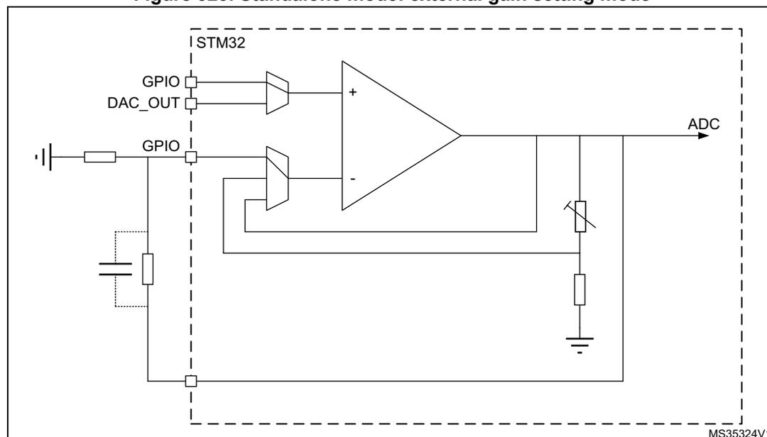
The diagram illustrates the standalone mode configuration of an OPAMP. A dashed box labeled 'STM32' contains internal components: a 'GPIO' pin, a 'DAC_OUT' pin, and another 'GPIO' pin. The 'DAC_OUT' pin is connected to the non-inverting input (+) of an operational amplifier. The inverting input (-) is connected to a 'GPIO' pin. The output of the operational amplifier is connected to an 'ADC'. Outside the 'STM32' box, the inverting input (-) is connected to a circuit consisting of a battery, a resistor, and a capacitor. The output of the operational amplifier is also connected to a circuit consisting of a resistor and a capacitor. The diagram is labeled 'MS35324V1' in the bottom right corner.
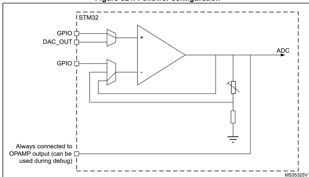
Follower configuration mode
The procedure to use the OPAMP in follower mode is detailed below (all bits in OPAMPx_CSR):
- 1. Set OPAMODE[1:0] = 11 (internal follower).
- 2. Clear VP_SEL to 0 (GPIO connected to OPAMPx_VINP, named VINP in this document).
- 3. As soon as OPAEN is set to 1, the signal on the VINP pin is copied to the OPAMP_VOUT pin.
Note: The pin corresponding to OPAMP_VINM is free for another usage.
The signal on the OPAMP output is also seen as an ADC input. As a consequence, the OPAMP configured in follower mode can be used to perform impedance adaptation on input signals before feeding them to the ADC input, assuming the input signal frequency is compatible with the operational amplifier gain bandwidth specification.
Figure 324. Follower configuration
Programmable gain amplifier mode
The procedure to use the OPAMP to amplify the amplitude of an input signal is presented hereafter (all bits in OPAMPx_CSR):
- 1. Set OPAMODE[1:0] to 10 (internal PGA enabled).
- 2. Set PGA_GAIN[1:0] to the selected PGA gain (2, 4, 8 or 16) in OPAMPx_CSR.
- 3. Set VM_SEL[1:0] to 1x in OPAMPx_CSR (inverting input not externally connected).
- 4. Clear VP_SEL to 0 in OPAMPx_CSR (GPIO connected to VINP).
- 5. As soon as OPAEN is set in OPAMPx_CSR, the signal on the OPAMP_VINP pin is amplified by the selected gain and visible on the OPAMP_VOUT pin.
Note: To avoid saturation, the input voltage must stay below \( V_{DDA} \) divided by the selected gain.
Figure 325. PGA mode, internal gain setting (x2/x4/x8/x16), inverting input not used
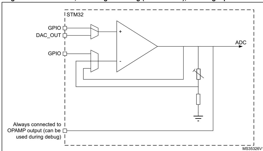
The diagram illustrates the internal configuration of an operational amplifier (OPAMP) within an STM32 microcontroller. The non-inverting input (+) is connected to a DAC_OUT pin. The inverting input (-) is connected to a GPIO pin and is also connected to the output through a feedback loop containing a variable resistor and a fixed resistor. The output is connected to an ADC. A note indicates that the output is always connected to the OPAMP output (can be used during debug). The diagram is labeled MS35326V1.
Programmable gain amplifier mode with external filtering
The procedure to use the OPAMP to amplify the amplitude of an input signal, with an external Set, is detailed below (all bits in OPAMPx_CSR):
- 1. Configure OPAMODE[1:0] to 10 (internal PGA enabled).
- 2. Set PGA_GAIN[1:0] to the selected PGA gain (2, 4, 8 or 16).
- 3. Clear VM_SEL[1:0] to 00 or 01(GPIO connected to VINM).
- 4. Clear VP_SEL to 0 (GPIO connected to VINP).
Any external connection on VINP can be used in parallel with the internal PGA. For example, a capacitor can be connected between VOUT and VINM for filtering purpose (see datasheet for the value of resistors used in the PGA resistor network).
Figure 326. PGA mode, internal gain setting (x2/x4/x8/x16), inverting input used for filtering
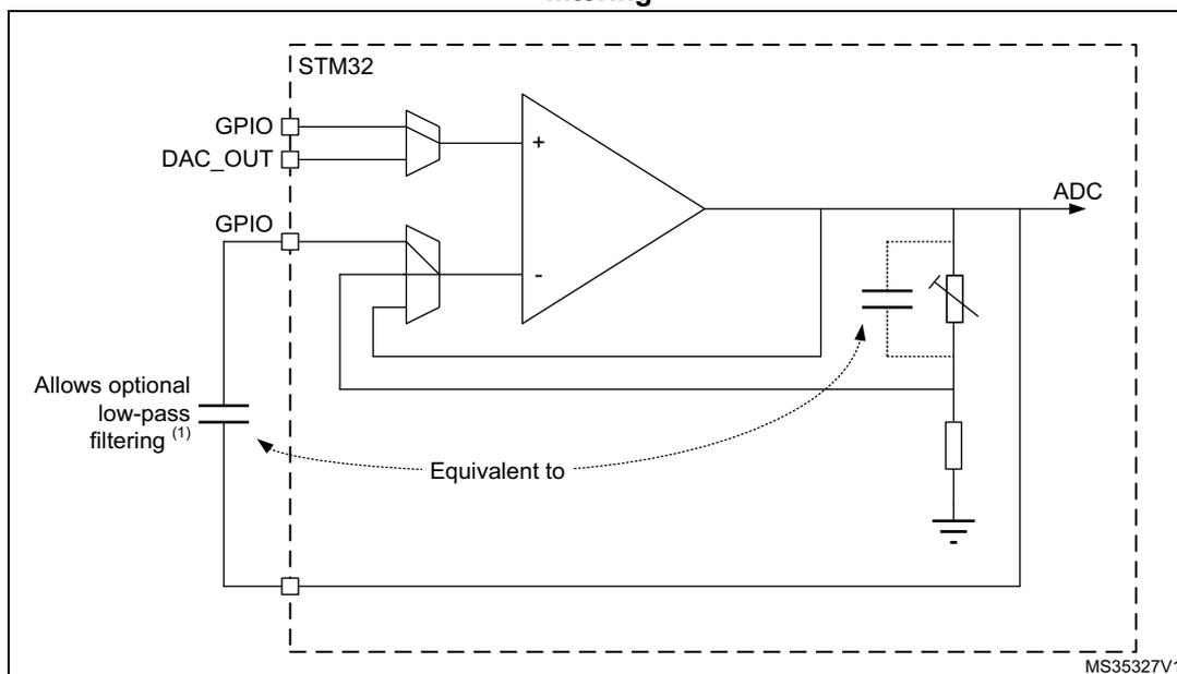
1. The gain depends on the cut-off frequency.
38.3.5 Calibration
At startup, the trimming values are initialized with the preset 'factory' trimming value.
Each OPAMP offset can be trimmed by the user. Specific registers allow different trimming values for normal and low-power modes.
The calibration purpose is to cancel as much as possible the OPAMP inputs offset voltage. The calibration circuitry allows the inputs offset voltage to be reduced to less than \( \pm 1.5 \) mV within stable voltage and temperature conditions.
For each OPAMP and each mode, two trimming values can be trimmed: one for N differential pair and one for P differential pair.
The registers used to trim the offsets for each operational amplifiers are:
- • OPAMPx_OTR for normal mode
- • OPAMPx_LPOTR for low-power mode
Each register is composed of five bits for P differential pair trimming and five bits for N differential pair trimming. These are the 'user' values.
The user is able to switch from 'factory' values to 'user' trimmed values, with the USERTRIM bit in OPAMPx_CSR. This bit is reset at startup and the 'factory' value are applied by default to the OPAMP trimming registers.
The trimming values can be changed in calibration or in functional mode.
The offset trimming registers are typically configured after the initialization of the calibration operation (CALON set to 1 in OPAMPx_CSR). When CALON = 1, the OPAMP inputs are disconnected from the functional environment.
Setting CALSEL to 1 in OPAMPx_CSR initializes the offset calibration for the P differential pair (low-voltage reference used).
Clearing CALSEL to 0 initializes the offset calibration for the N differential pair (high voltage reference used).
When CALON = 1, the CALOUT bit in OPAMPx_CSR reflects the influence of the trimming value selected by CALSEL and OPALPM. When the value of CALOUT switches between two consecutive trimming values, this means that those two values are the best trimming values. The CALOUT flag needs up to 1 ms after the trimming value is changed to become steady (see \( t_{\text{OFFTRIM}} \) max delay specification in the “electrical characteristics” section of the datasheet).
Note: The closer the trimming value is to the optimum trimming value, the longer it takes to stabilize (with a maximum stabilization time remaining below 1 ms in any case).
When the calibration operation is done, OPAHSM must be cleared to 0 in OPAMPx_CSR.
Table 364. Operating modes and calibration
| Mode | Control bits | Output | ||||
|---|---|---|---|---|---|---|
| OPAEN | OPALPM | CALON | CALSEL | V OUT | CALOUT | |
| Normal operating mode | 1 | 0 | 0 | X | Analog | 0 |
| Low-power mode | 1 | 1 | 0 | X | Analog | 0 |
| Power down | 0 | X | X | X | Z | 0 |
| Offset cal high for normal mode | 1 | 0 | 1 | 0 | Analog | X |
| Offset cal low for normal mode | 1 | 0 | 1 | 1 | Analog | X |
| Offset cal high for low-power mode | 1 | 1 | 1 | 0 | Analog | X |
| Offset cal low for low-power mode | 1 | 1 | 1 | 1 | Analog | X |
Calibration procedure
Here are the steps to perform a full calibration of either one of the operational amplifiers:
- 1. Set OPAEN to 1 in OPAMPx_CSR to enable the OPAMP and set OPA_RANGE = 1 in OPAMP1_CSR.
- 2. Clear OPAHSM to 0 in OPAMPx_CSR.
- 3. Set CALON and USERTRIM to 1 in OPAMPx_CSR.
- 4. Choose a calibration mode (refer to Table 364 ). Steps 4 to 5 must be repeated four times. For the first iteration, select normal mode, offset cal high (N differential pair), with OPALPM = 0 and CALSEL = 0 in OPAMPx_CSR.
- 5. Increment TRIMOFFSETN[4:0] in OPAMPx_OTR starting from 0, until CALOUT changes to 1 in OPAMPx_CSR.
Between the write to OPAMP_OTR and the read of the CALOUT value, make sure to wait for the \( t_{\text{OFFTRIM}} \) max delay specified in the “electrical characteristics” section of the datasheet, to get the correct CALOUT value.
The commutation means that the offset is correctly compensated and that the corresponding trim code must be saved in OPAMP_OTR.
6. Repeat steps 4 to 5 for:
- – normal mode and offset cal low
- – low-power mode and offset cal high
- – low-power mode and offset cal low
If a mode is not used, the corresponding calibration can be skipped.
All OPAMPs can be calibrated at the same time.
Note: During the whole calibration phase:
- - the external connection of the OPAMP output must not pull up or down currents higher than 500 \( \mu\text{A} \) .
- - OPAMODE[1:0] must be set up to 00 or 01 (PGA disable) or 11 (internal follower).
38.4 OPAMP low-power modes
Table 365. Effect of low-power modes on the OPAMP
| Mode | Description |
|---|---|
| Sleep | No effect. |
| Stop0/1/2 | No effect, OPAMP registers content is kept. |
| Stop3 | The OPAMP is disabled; the register content is kept. |
| Standby | The OPAMP registers are powered down and must be re-initialized after exiting Standby mode. |
38.5 OPAMP registers
These registers are only accessible by word.(byte and half-word not supported)
38.5.1 OPAMP1 control/status register (OPAMP1_CSR)
Address offset: 0x00
Reset value: 0x0000 0000
| 31 | 30 | 29 | 28 | 27 | 26 | 25 | 24 | 23 | 22 | 21 | 20 | 19 | 18 | 17 | 16 |
|---|---|---|---|---|---|---|---|---|---|---|---|---|---|---|---|
| OPA_R ANGE | OPAHS M | Res. | Res. | Res. | Res. | Res. | Res. | Res. | Res. | Res. | Res. | Res. | Res. | Res. | Res. |
| rw | rw |
| 15 | 14 | 13 | 12 | 11 | 10 | 9 | 8 | 7 | 6 | 5 | 4 | 3 | 2 | 1 | 0 |
|---|---|---|---|---|---|---|---|---|---|---|---|---|---|---|---|
| CALOU T | USER TRIM | CALSE L | CALON | Res. | VP_SE L | VM_SEL[1:0] | Res. | Res. | PGA_GAIN[1:0] | OPAMODE[1:0] | OPALP M | OPAEN | |||
| r | rw | rw | rw | rw | rw | rw | rw | rw | rw | rw | rw | rw | rw |
Bit 31 OPA_RANGE : OPAMP range setting
This bit must be set before enabling the OPAMP and this bit affects all OPAMP instances.
0: reserved
1: OPAMP range set
- Bit 30
OPAHSM
: OPAMP high-speed mode
- This bit is effective for both normal and low-power modes.
- 0: normal mode (standard slew rate)
- 1: increased consumption to improve the slew rate
- Bits 29:16 Reserved, must be kept at reset value.
- Bit 15
CALOUT
: OPAMP calibration output
- During the calibration mode, the offset is trimmed when this signal toggles.
- Bit 14
USERTRIM
: 'factory' or 'user' offset trimmed values selection
- This bit is active for normal and low-power modes.
- 0: 'factory' trim code used
- 1: 'user' trim code used
- Bit 13
CALSEL
: Calibration selection
- 0: NMOS calibration (200 mV applied on OPAMP inputs)
- 1: PMOS calibration ( \( V_{DDA} - 200 \) mV applied on OPAMP inputs)
- Bit 12
CALON
: Calibration mode enable
- 0: normal mode
- 1: calibration mode (all switches opened by hardware)
- Bit 11 Reserved, must be kept at reset value.
- Bit 10
VP_SEL
: Non-inverted input selection
- 0: GPIO connected to VINP
- 1: DAC connected to VINP
- Bits 9:8
VM_SEL[1:0]
: Inverting input selection
- These bits are used only when OPAMODE = 00, 01 or 10.
- 00: GPIO connected to VINM (valid also in PGA mode for filtering)
- 01: dedicated low-leakage input connected to VINM (valid also in PGA mode for filtering)
- 1x: inverting input not externally connected
- Bits 7:6 Reserved, must be kept at reset value.
- Bits 5:4
PGA_GAIN[1:0]
: OPAMP programmable amplifier gain value
- 00: internal PGA gain 2
- 01: internal PGA gain 4
- 10: internal PGA gain 8
- 11: internal PGA gain 16
- Bits 3:2
OPAMODE[1:0]
: OPAMP PGA mode
- 00 and 01: internal PGA disabled
- 10: internal PGA enabled, gain programmed in PGA_GAIN
- 11: internal follower
- Bit 1
OPALPM
: OPAMP low-power mode
- The OPAMP must be disabled to change this configuration.
- 0: normal mode
- 1: low-power mode
- Bit 0
OPAEN
: OPAMP enable
- 0: OPAMP disabled
- 1: OPAMP enabled
38.5.2 OPAMP1 offset trimming register in normal mode (OPAMP1_OTR)
Address offset: 0x04
Reset value: 0x0000 XXXX
XXXX are factory trimmed values.
| 31 | 30 | 29 | 28 | 27 | 26 | 25 | 24 | 23 | 22 | 21 | 20 | 19 | 18 | 17 | 16 |
|---|---|---|---|---|---|---|---|---|---|---|---|---|---|---|---|
| Res. | Res. | Res. | Res. | Res. | Res. | Res. | Res. | Res. | Res. | Res. | Res. | Res. | Res. | Res. | Res. |
| 15 | 14 | 13 | 12 | 11 | 10 | 9 | 8 | 7 | 6 | 5 | 4 | 3 | 2 | 1 | 0 |
| Res. | Res. | Res. | TRIMOFFSETP[4:0] | Res. | Res. | Res. | TRIMOFFSETN[4:0] | ||||||||
| rw | rw | rw | rw | rw | rw | rw | rw | rw | rw | ||||||
Bits 31:13 Reserved, must be kept at reset value.
Bits 12:8 TRIMOFFSETP[4:0] : Trim for PMOS differential pairs
Bits 7:5 Reserved, must be kept at reset value.
Bits 4:0 TRIMOFFSETN[4:0] : Trim for NMOS differential pairs
38.5.3 OPAMP1 offset trimming register in low-power mode (OPAMP1_LPOTR)
Address offset: 0x08
Reset value: 0x0000 XXXX
XXXX are factory trimmed values.
| 31 | 30 | 29 | 28 | 27 | 26 | 25 | 24 | 23 | 22 | 21 | 20 | 19 | 18 | 17 | 16 |
|---|---|---|---|---|---|---|---|---|---|---|---|---|---|---|---|
| Res. | Res. | Res. | Res. | Res. | Res. | Res. | Res. | Res. | Res. | Res. | Res. | Res. | Res. | Res. | Res. |
| 15 | 14 | 13 | 12 | 11 | 10 | 9 | 8 | 7 | 6 | 5 | 4 | 3 | 2 | 1 | 0 |
| Res. | Res. | Res. | TRIMLPOFFSETP[4:0] | Res. | Res. | Res. | TRIMLPOFFSETN[4:0] | ||||||||
| rw | rw | rw | rw | rw | rw | rw | rw | rw | rw | ||||||
Bits 31:13 Reserved, must be kept at reset value.
Bits 12:8 TRIMLPOFFSETP[4:0] : Low-power mode trim for PMOS differential pairs
Bits 7:5 Reserved, must be kept at reset value.
Bits 4:0 TRIMLPOFFSETN[4:0] : Low-power mode trim for NMOS differential pairs
38.5.4 OPAMP2 control/status register (OPAMP2_CRS)
Address offset: 0x10
Reset value: 0x0000 0000
This register availability varies in STM32U5 Series devices. Refer to Section 38.1 . If not present, consider it as reserved and keep it at reset value.
| 31 | 30 | 29 | 28 | 27 | 26 | 25 | 24 | 23 | 22 | 21 | 20 | 19 | 18 | 17 | 16 |
|---|---|---|---|---|---|---|---|---|---|---|---|---|---|---|---|
| Res. | OPAHS M | Res. | Res. | Res. | Res. | Res. | Res. | Res. | Res. | Res. | Res. | Res. | Res. | Res. | Res. |
| 15 | 14 | 13 | 12 | 11 | 10 | 9 | 8 | 7 | 6 | 5 | 4 | 3 | 2 | 1 | 0 |
| CALOUT T | USERTR IM | CALSE L | CALON | Res. | VP_SE L | VM_SEL[1:0] | Res. | Res. | PGA_GAIN[1:0] | OPAMODE[1:0] | OPALP M | OPAEN | |||
| r | rw | rw | rw | rw | rw | rw | rw | rw | rw | rw | rw | rw | |||
Bit 31 Reserved, must be kept at reset value.
Bit 30 OPAHSM : OPAMP high-speed mode
This bit is effective for both normal and high-speed modes.
0: normal mode (standard slew rate)
1: increased consumption to improve the slew rate
Bits 29:16 Reserved, must be kept at reset value.
Bit 15 CALOUT : OPAMP calibration output
During calibration mode, the offset is trimmed when this signal toggles.
Bit 14 USERTRIM : 'factory' or 'user' offset trimmed values selection
This bit is active for normal and low-power modes.
0: 'factory' trim code used
1: 'user' trim code used
Bit 13 CALSEL : Calibration selection
0: NMOS calibration (200 mV applied on OPAMP inputs)
1: PMOS calibration ( \( V_{DDA} - 200 \) mV applied on OPAMP inputs)
Bit 12 CALON : Calibration mode enable
0: normal mode
1: calibration mode (all switches opened by hardware)
Bit 11 Reserved, must be kept at reset value.
Bit 10 VP_SEL : Non inverted input selection
0: GPIO connected to VINP
1: DAC connected to VINP
Bits 9:8 VM_SEL[1:0] : Inverting input selection
These bits are used only when OPAMODE = 00, 01 or 10.
00: GPIO connected to VINM (valid also in PGA mode for filtering)
01: dedicated low-leakage input connected to VINM (valid also in PGA mode for filtering)
1x: inverting input not externally connected
Bits 7:6 Reserved, must be kept at reset value.
Bits 5:4 PGA_GAIN[1:0] : OPAMP programmable amplifier gain value
- 00: internal PGA gain 2
- 01: internal PGA gain 4
- 10: internal PGA gain 8
- 11: internal PGA gain 16
Bits 3:2 OPAMODE[1:0] : OPAMP PGA mode
- 00 and 01: internal PGA disabled
- 10: internal PGA enabled, gain programmed in PGA_GAIN
- 11: internal follower
Bit 1 OPALPM : OPAMP low-power mode
The OPAMP must be disabled to change this configuration.
- 0: normal mode
- 1: low-power mode
Bit 0 OPAEN : OPAMP enable
- 0: OPAMP disabled
- 1: OPAMP enabled
38.5.5 OPAMP2 offset trimming register in normal mode (OPAMP2_OTR)
Address offset: 0x14
Reset value: 0x0000 XXXX
XXXX are factory trimmed values.
This register availability varies in STM32U5 Series devices. Refer to Section 38.1 . If not present, consider it as reserved and keep it at reset value.
| 31 | 30 | 29 | 28 | 27 | 26 | 25 | 24 | 23 | 22 | 21 | 20 | 19 | 18 | 17 | 16 |
|---|---|---|---|---|---|---|---|---|---|---|---|---|---|---|---|
| Res. | Res. | Res. | Res. | Res. | Res. | Res. | Res. | Res. | Res. | Res. | Res. | Res. | Res. | Res. | Res. |
| 15 | 14 | 13 | 12 | 11 | 10 | 9 | 8 | 7 | 6 | 5 | 4 | 3 | 2 | 1 | 0 |
| Res. | Res. | Res. | TRIMOFFSETP[4:0] | Res. | Res. | Res. | TRIMOFFSETN[4:0] | ||||||||
| rw | rw | rw | rw | rw | rw | rw | rw | rw | rw | ||||||
Bits 31:13 Reserved, must be kept at reset value.
Bits 12:8 TRIMOFFSETP[4:0] : Trim for PMOS differential pairs
Bits 7:5 Reserved, must be kept at reset value.
Bits 4:0 TRIMOFFSETN[4:0] : Trim for NMOS differential pairs
38.5.6 OPAMP2 offset trimming register in low-power mode (OPAMP2_LPOTR)
Address offset: 0x18
Reset value: 0x0000 XXXX
XXXX are factory trimmed values.
This register availability varies in STM32U5 Series devices. Refer to Section 38.1 . If not present, consider it as reserved and keep it at reset value.
| 31 | 30 | 29 | 28 | 27 | 26 | 25 | 24 | 23 | 22 | 21 | 20 | 19 | 18 | 17 | 16 |
|---|---|---|---|---|---|---|---|---|---|---|---|---|---|---|---|
| Res. | Res. | Res. | Res. | Res. | Res. | Res. | Res. | Res. | Res. | Res. | Res. | Res. | Res. | Res. | Res. |
| 15 | 14 | 13 | 12 | 11 | 10 | 9 | 8 | 7 | 6 | 5 | 4 | 3 | 2 | 1 | 0 |
| Res. | Res. | Res. | TRIMLPOFFSETP[4:0] | Res. | Res. | Res. | TRIMLPOFFSETN[4:0] | ||||||||
| rw | rw | rw | rw | rw | rw | rw | rw | rw | rw | ||||||
Bits 31:13 Reserved, must be kept at reset value.
Bits 12:8 TRIMLPOFFSETP[4:0] : Low-power mode trim for PMOS differential pairs
Bits 7:5 Reserved, must be kept at reset value.
Bits 4:0 TRIMLPOFFSETN[4:0] : Low-power mode trim for NMOS differential pairs
38.5.7 OPAMP register map
Table 366. OPAMP register map and reset values
| Offset | Register name | 31 | 30 | 29 | 28 | 27 | 26 | 25 | 24 | 23 | 22 | 21 | 20 | 19 | 18 | 17 | 16 | 15 | 14 | 13 | 12 | 11 | 10 | 9 | 8 | 7 | 6 | 5 | 4 | 3 | 2 | 1 | 0 |
|---|---|---|---|---|---|---|---|---|---|---|---|---|---|---|---|---|---|---|---|---|---|---|---|---|---|---|---|---|---|---|---|---|---|
| 0x00 | OPAMP1_CSR | OPA_RANGE | OPA_HSM | Res. | Res. | Res. | Res. | Res. | Res. | Res. | Res. | Res. | Res. | Res. | Res. | Res. | Res. | CALOUT | USERTRIM | CALSEL | CALON | Res. | VP_SEL | VM_SEL[1:0] | Res. | Res. | Res. | PGA_GAIN[1:0] | OPAMODE[1:0] | OPALPM | OPAEN | ||
| Reset value | 0 | 0 | 0 | 0 | 0 | 0 | 0 | 0 | 0 | 0 | 0 | 0 | 0 | 0 | 0 | ||||||||||||||||||
| 0x04 | OPAMP1_OTR | Res. | Res. | Res. | Res. | Res. | Res. | Res. | Res. | Res. | Res. | Res. | Res. | Res. | Res. | Res. | Res. | Res. | Res. | Res. | TRIM OFFSETP[4:0] | Res. | Res. | Res. | Res. | TRIM OFFSETN[4:0] | |||||||
| Reset value | X | X | X | X | X | X | X | X | X | ||||||||||||||||||||||||
| 0x08 | OPAMP1_LPOTR | Res. | Res. | Res. | Res. | Res. | Res. | Res. | Res. | Res. | Res. | Res. | Res. | Res. | Res. | Res. | Res. | Res. | Res. | Res. | TRIML OFFSETP[4:0] | Res. | Res. | Res. | Res. | TRIML OFFSETN[4:0] | |||||||
| Reset value | X | X | X | X | X | X | X | X | X | ||||||||||||||||||||||||
| 0x10 | OPAMP2_CSR | Res. | OPA_HSM | Res. | Res. | Res. | Res. | Res. | Res. | Res. | Res. | Res. | Res. | Res. | Res. | Res. | Res. | CALOUT | USERTRIM | CALSEL | CALON | Res. | VP_SEL | VM_SEL[1:0] | Res. | Res. | Res. | PGA_GAIN[1:0] | OPAMODE[1:0] | OPALPM | OPAEN | ||
| Reset value | 0 | 0 | 0 | 0 | 0 | 0 | 0 | 0 | 0 | 0 | 0 | 0 | 0 | 0 | |||||||||||||||||||
| 0x14 | OPAMP2_OTR | Res. | Res. | Res. | Res. | Res. | Res. | Res. | Res. | Res. | Res. | Res. | Res. | Res. | Res. | Res. | Res. | Res. | Res. | Res. | TRIM OFFSETP[4:0] | Res. | Res. | Res. | Res. | TRIM OFFSETN[4:0] | |||||||
| Reset value | X | X | X | X | X | X | X | X | X | ||||||||||||||||||||||||
Table 366. OPAMP register map and reset values (continued)
| Offset | Register name | 31 | 30 | 29 | 28 | 27 | 26 | 25 | 24 | 23 | 22 | 21 | 20 | 19 | 18 | 17 | 16 | 15 | 14 | 13 | 12 | 11 | 10 | 9 | 8 | 7 | 6 | 5 | 4 | 3 | 2 | 1 | 0 |
|---|---|---|---|---|---|---|---|---|---|---|---|---|---|---|---|---|---|---|---|---|---|---|---|---|---|---|---|---|---|---|---|---|---|
| 0x18 | OPAMP2_LPOTR | Res | Res | Res | Res | Res | Res | Res | Res | Res | Res | Res | Res | Res | Res | Res | Res | Res | Res | Res | TRIMLP OFFSETN[4:0] | Res | Res | Res | TRIMLP OFFSETN[4:0] | ||||||||
| Reset value | X | X | X | X | X | X | X | X | X | X | |||||||||||||||||||||||
Refer to Section 2.3 for the register boundary addresses.