37. Comparator (COMP)
37.1 Introduction
The device embeds two ultra-low-power comparators COMP1 and COMP2.
These comparators can be used for a variety of functions including:
- • Wake-up from low-power mode triggered by an analog signal
- • Analog signal conditioning
- • Cycle-by-cycle current control loop when combined with a PWM output from a timer
37.2 COMP main features
- • Each comparator has configurable plus and minus inputs used for flexible voltage selection:
- – Multiplexed I/O pins
- – DAC channel1 and channel2
- – Internal reference voltage and three submultiple values (1/4, 1/2, 3/4) provided by a scaler (buffered voltage divider)
- • Programmable hysteresis
- • Programmable speed/consumption
- • Outputs that can be redirected to an I/O or to timer inputs for triggering break events for fast PWM shutdowns
- • Comparator outputs with blanking source
- • Comparators that can be combined as a window comparator
- • Interrupt generation capability for each comparator with wake-up from Sleep and Stop modes (through the EXTI controller)
37.3 COMP implementation
The following table describes COMP features on the STM32U5 Series devices.
Table 353. COMP features (1)
| COMP modes/features | STM32U535/545 | Other devices |
|---|---|---|
| COMP1 | X | X |
| COMP1 INPy maximum input | y = 6 | y = 3 |
| COMP1_INPSEL[2:0] reserved codes | ≥ 101 | ≥ 011 |
| COMP2 | - | X |
| Window comparator feature | - | X |
- 1. 'X' = supported
'-' = non supported
37.4 COMP functional description
37.4.1 COMP block diagram
The block diagram of the comparators is shown in the figure below.
Figure 318. Comparator block diagrams
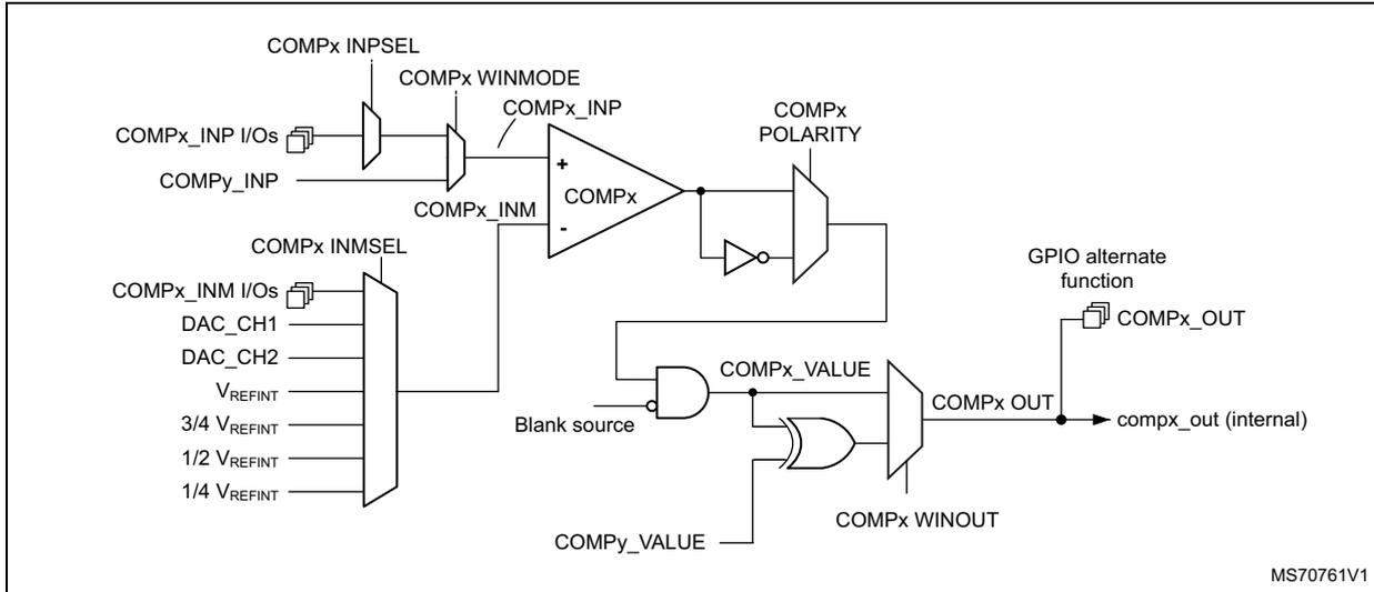
37.4.2 COMP pins and internal signals
The I/Os used as comparators inputs must be configured in analog mode in the GPIOs registers.
The comparator output can be connected to the I/Os using the alternate function channel given in “Alternate function mapping” table in the datasheet.
The output can also be internally redirected to a variety of timer input for the following purposes:
- • Emergency shut-down of PWM signals, using BKIN and BKIN2 inputs
- • Cycle-by-cycle current control, using OCREF_CLR inputs
- • Input capture for timing measures
The comparator output can be simultaneously redirected internally and externally.
Table 354. COMP1 non-inverting input assignment
| COMP1_INP | COMP1_INPSEL[2:0] |
|---|---|
| COMP1_INP1 | 000 |
| COMP1_INP2 | 001 |
| COMP1_INP3 | 010 |
| COMP1_INP4 | 011 |
| COMP1_INP5 | 100 |
| COMP1_INP6 | 101 |
Table 355. COMP1 inverting input assignment
| COMP1_INM | COMP1_INMSEL[3:0] |
|---|---|
| \( \frac{1}{4} \) V REFINT | 0000 |
| \( \frac{1}{2} \) V REFINT | 0001 |
| \( \frac{3}{4} \) V REFINT | 0010 |
| V REFINT | 0011 |
| DAC Channel1 | 0100 |
| DAC Channel2 | 0101 |
| COMP1_INM1 | 0110 |
| COMP1_INM2 | 0111 |
| Reserved | \( \geq 1000 \) |
Table 356. COMP2 non-inverting input assignment
| COMP2_INP | COMP2_INPSEL[1:0] |
|---|---|
| COMP2_INP1 | 00 |
| COMP2_INP2 | 01 |
| Reserved | 10 |
| Reserved | 11 |
Table 357. COMP2 inverting input assignment
| COMP2_INM | COMP2_INMSEL[3:0] |
|---|---|
| \( \frac{1}{4} \) V REFINT | 0000 |
| \( \frac{1}{2} \) V REFINT | 0001 |
| \( \frac{3}{4} \) V REFINT | 0010 |
| V REFINT | 0011 |
| DAC Channel1 | 0100 |
| DAC Channel2 | 0101 |
| COMP2_INM1 | 0110 |
| COMP2_INM2 | 0111 |
| Reserved | \( \geq 1000 \) |
Table 358. COMP1 output-blanking PWM assignment
| PWM output | COMP1_BLANKSEL[4:0] |
|---|---|
| None (no blanking) | 00000 |
| tim1_oc5 | xxx1 |
| tim2_oc3 | xxx1x |
| PWM output | COMP1_BLANKSEL[4:0] |
|---|---|
| tim3_oc3 | xx1xx |
| Reserved | Others |
| PWM output | COMP2_BLANKSEL[4:0] |
|---|---|
| None (no blanking) | 00000 |
| tim3_oc4 | xxxx1 |
| tim8_oc5 | xxx1x |
| tim15_oc1 | xx1xx |
| Reserved | Others |
37.4.3 Comparator LOCK mechanism
The comparators can be used for safety purposes, such as over-current or thermal protection. For applications having specific functional safety requirements, the comparator programming must not be altered in case of spurious register access or program counter corruption. For this purpose, the comparator control and status registers can be write-protected (read-only).
Once the programming is completed, the COMPxLOCK bit can be set to 1. This causes the whole COMPx_CSR register to become read-only, including the COMPxLOCK bit.
The write protection can only be reset by an MCU reset.
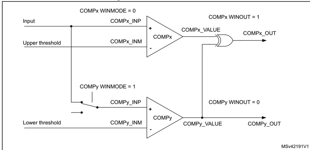
37.4.4 Window comparator
The purpose of the window comparator is to monitor the analog voltage if it is within the voltage range defined by the lower and upper threshold.
The two embedded comparators can be used to create a window comparator. The monitored analog voltage is connected to the non-inverting (plus) inputs of comparators connected together. The upper and lower threshold voltages are connected to the inverting (minus) inputs of the comparators.
Two non-inverting inputs can be connected internally together by enabling the WINMODE bit to save one IO for other purposes.
Figure 319. Window mode
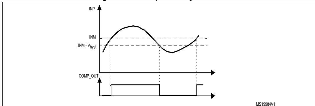
37.4.5 Hysteresis
The comparator includes a programmable hysteresis to avoid spurious output transitions in case of noisy signals. The hysteresis can be disabled if it is not needed (for instance when exiting a low-power mode) to be able to force the hysteresis value using external components.
Figure 320. Comparator hysteresis
37.4.6 Comparator output-blanking function
The blanking function prevents the current regulation to trip upon short current spikes at the beginning of the PWM period (typically the recovery current in power switches anti parallel diodes). This blanking function consists of a selection of a blanking window that is a timer output compare signal. The selection is done by the software (refer to the comparator register description for possible blanking signals).
The complementary of the blanking signal is ANDed with the comparator output to provide the wanted comparator output (see the example in the figure below).
Figure 321. Comparator output blanking
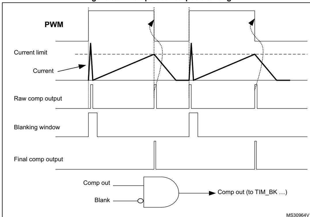
The figure illustrates the comparator output blanking mechanism. The top part is a timing diagram showing the relationship between the PWM signal, the current limit, the actual current, the raw comparator output, the blanking window, and the final comparator output. The bottom part is a logic schematic showing the AND gate that combines the raw comparator output and the inverted blanking window to produce the final output.
37.4.7 COMP power and speed modes
COMP1 and COMP2 power consumption versus propagation delay can be adjusted to have the optimum trade-off for a given application.
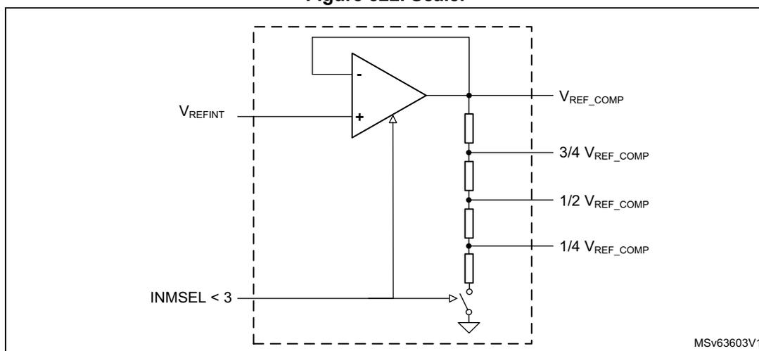
37.4.8 Scaler function
The scaler block provides the different voltage reference levels to the comparator inputs. This block is based on an amplifier driving a resistor bridge. The amplifier input is connected to the internal voltage reference. The amplifier and the resistor bridge are enabled by setting the INMSEL value in the COMP_CFGRx registers, to connect the corresponding inverting input to the scaler output.
When the resistor divided voltage is not used, the resistor bridge and the amplifier are disabled to reduce the consumption. When the resistor bridge is disconnected, the 1/4 VREF_COMP, 1/2 VREF_COMP, and 3/4 VREF_COMP levels are equal to VREF_COMP.
Figure 322. Scaler
37.5 COMP low-power modes
Table 360. Comparator behavior in the low-power modes
| Mode | Description |
|---|---|
| Sleep | No effect on the comparators. Comparator interrupts cause the device to exit Sleep mode. |
| Stop | No effect on the comparators. Comparator interrupts cause the device to exit Stop mode. |
| Standby | The COMP registers are powered down and must be reinitialized after exiting Standby mode. |
37.6 COMP interrupts
The comparator outputs are internally connected to the extended interrupts and events controller (EXTI). Each comparator has its own EXTI line and can generate either interrupts or events. The same mechanism is used to exit the low-power modes.
Refer to Section 23: Extended interrupts and event controller (EXTI) for more details.
To enable the COMPx interrupt, follow this sequence:
- 1. Configure and enable the EXTI line corresponding to the COMPx output event in interrupt mode and select the rising, falling or both edges sensitivity.
- 2. Configure and enable the NVIC IRQ channel mapped to the corresponding EXTI lines.
- 3. Enable the COMPx.
Table 361. Interrupt control bits
| Interrupt event | Event flag | Enable control bit | Exit Sleep mode | Exit Stop modes | Exit Standby mode |
|---|---|---|---|---|---|
| COMP1 output | VALUE in COMP1_CSR | through EXTI | Yes | Yes | No |
| COMP2 output | VALUE in COMP2_CSR | through EXTI | Yes | Yes | No |
37.7 COMP registers
37.7.1 COMP1 control and status register (COMP1_CSR)
Address offset: 0x00
Reset value: 0x0000 0000
| 31 | 30 | 29 | 28 | 27 | 26 | 25 | 24 | 23 | 22 | 21 | 20 | 19 | 18 | 17 | 16 |
|---|---|---|---|---|---|---|---|---|---|---|---|---|---|---|---|
| LOCK | VALUE | Res. | Res. | Res. | Res. | Res. | BLANKSEL[4:0] | PWRMODE[1:0] | HYST[1:0] | ||||||
| rw | r | rw | rw | rw | rw | rw | rw | rw | rw | rw | |||||
| 15 | 14 | 13 | 12 | 11 | 10 | 9 | 8 | 7 | 6 | 5 | 4 | 3 | 2 | 1 | 0 |
|---|---|---|---|---|---|---|---|---|---|---|---|---|---|---|---|
| POLARITY | WINOUT | Res. | Res. | WIN MODE | INPSEL[2:0] | INMSEL[3:0] | Res. | Res. | Res. | Res. | EN | ||||
| rw | rw | rw | rw | rw | rw | rw | rw | rw | rw | rw | |||||
Bit 31 LOCK : COMP1_CSR register lock
This bit is set by the software and cleared by reset. It locks the whole content of COMP1_CSR.
0: COMP1_CSR read/write bits can be written by the software.
1: COMP1_CSR bits can be read but not written by the software.
Bit 30 VALUE : COMP1 output status
This bit is read-only. It reflects the level of the COMP1 output after the polarity selector and blanking (see Figure 321 ).
Bits 29:25 Reserved, must be kept at reset value.
Bits 24:20 BLANKSEL[4:0] : COMP1 blanking source selector
This field is controlled by the software (if not locked) and selects the PWM signal for comparator output-blanking (see Table 358 for the assignment).
Bits 19:18 PWRMODE[1:0] : COMP1 power mode selector
This bitfield is controlled by the software (if not locked). It selects the power consumption and, as a consequence, the speed of the COMP1.
00: High speed
01-10: Medium speed and power
11: Ultra-low-power
Bits 17:16 HYST[1:0] : COMP1 hysteresis selector
This bitfield is controlled by the software (if not locked). It selects the COMP1 hysteresis.
00: None
01: Low hysteresis
10: Medium hysteresis
11: High hysteresis
Bit 15 POLARITY : COMP1 polarity selector
This bit is controlled by the software (if not locked). It selects the COMP1 output polarity.
0: Non-inverted
1: Inverted
Bit 14 WINOUT : COMP1 output selector
This bit is controlled by the software (if not locked). It selects the COMP1 output.
This bit must be kept at zero when window comparator feature is not supported.
0: COMP1_VALUE
1: COMP1_VALUE XOR COMP2_VALUE (required for window mode, see Figure 319 )
Bits 13:12 Reserved, must be kept at reset value.
Bit 11 WINMODE : COMP1 non-inverting input selector for window mode
This bit is controlled by the software (if not locked). It selects the signal for the COMP1_INP input of the COMP1.
This bit must be kept at zero when window comparator feature is not supported.
0: Signal selected with INPSEL[1:0]
1: COMP2_INP signal of COMP2 (required for window mode, see Figure 319 )
Bits 10:8 INPSEL[2:0] : COMP1 signal selector for non-inverting input
This field is controlled by the software (if not locked). It selects the signal for the non-inverting input COMP1_INP (see Table 354 for the assignment).
Bits 7:4 INMSEL[3:0] : COMP1 signal selector for inverting input INM
This field is controlled by the software (if not locked). It selects the signal for the inverting input COMP1_INM (see Table 355 for the assignment).
Bits 3:1 Reserved, must be kept at reset value.
Bit 0 EN : COMP1 enable
This bit is controlled by the software (if not locked). It enables COMP1.
0: COMP1 disabled
1: COMP1 enabled
37.7.2 COMP2 control and status register (COMP2_CSR)
Address offset: 0x04
Reset value: 0x0000 0000
| 31 | 30 | 29 | 28 | 27 | 26 | 25 | 24 | 23 | 22 | 21 | 20 | 19 | 18 | 17 | 16 |
|---|---|---|---|---|---|---|---|---|---|---|---|---|---|---|---|
| LOCK | VALUE | Res. | Res. | Res. | Res. | Res. | BLANKSEL[4:0] | PWRMODE[1:0] | HYST[1:0] | ||||||
| rw | r | rw | rw | rw | rw | rw | rw | rw | rw | rw | |||||
| 15 | 14 | 13 | 12 | 11 | 10 | 9 | 8 | 7 | 6 | 5 | 4 | 3 | 2 | 1 | 0 |
|---|---|---|---|---|---|---|---|---|---|---|---|---|---|---|---|
| POLARITY | WIN OUT | Res. | Res. | WIN MODE | Res. | INPSEL[1:0] | INMSEL[3:0] | Res. | Res. | Res. | EN | ||||
| rw | rw | rw | rw | rw | rw | rw | rw | rw | rw | ||||||
Bit 31 LOCK : COMP2_CSR register lock
This bit is set by the software and cleared by reset. It locks the whole content of COMP2_CSR.
0: COMP2_CSR read/write bits can be written by the software.
1: COMP2_CSR bits can be read but not written by the software.
Bit 30 VALUE : COMP2 output status
This bit is read-only. It reflects the level of the COMP2 output after the polarity selector and blanking (see Figure 321 ).
Bits 29:25 Reserved, must be kept at reset value.
Bits 24:20 BLANKSEL[4:0] : COMP2 blanking source selector
This field is controlled by the software (if not locked) and selects the PWM signal for comparator output-blanking (see Table 359 for the assignment).
Bits 19:18 PWRMODE[1:0] : COMP2 power mode selector
This bitfield is controlled by the software (if not locked). It selects the power consumption and, as a consequence, the speed of the COMP2.
00: High speed
01-10: Medium speed and power
11: Ultra-low-power
Bits 17:16 HYST[1:0] : COMP2 hysteresis selector
This bitfield is controlled by the software (if not locked). It selects the COMP2 hysteresis.
00: None
01: Low hysteresis
10: Medium hysteresis
11: High hysteresis
Bit 15 POLARITY : COMP2 polarity selector
This bit is controlled by the software (if not locked). It selects the COMP2 output polarity.
0: Non-inverted
1: Inverted
Bit 14 WINOUT : COMP2 output selector
This bit is controlled by the software (if not locked). It selects the COMP2 output.
0: COMP2_VALUE
1: COMP1_VALUE XOR COMP2_VALUE (required for window mode, see Figure 319 )
Bits 13:12 Reserved, must be kept at reset value.
Bit 11 WINMODE : COMP2 non-inverting input selector for window mode
This bit is controlled by the software (if not locked). It selects the signal for the COMP2_INP input of the COMP2.
0: Signal selected with INPSEL[1:0]
1: COMP1_INP signal of COMP1 (required for window mode, see Figure 319 )
Bit 10 Reserved, must be kept at reset value.
Bits 9:8 INPSEL[1:0] : COMP2 signal selector for non-inverting input
This field is controlled by the software (if not locked). It selects the signal for the non-inverting input COMP2_INP (see Table 356 for the assignment).
Bits 7:4 INMSEL[3:0] : COMP2 signal selector for inverting input INM
This field is controlled by the software (if not locked). It selects the signal for the inverting input COMP2_INM (see Table 357 for the assignment).
Bits 3:1 Reserved, must be kept at reset value.
Bit 0 EN : COMP2 enable
This bit is controlled by the software (if not locked). It enables COMP2.
0: COMP2 disabled
1: COMP2 enabled
37.7.3 COMP register map
Table 362. COMP register map and reset values
| Offset | Register name | 31 | 30 | 29 | 28 | 27 | 26 | 25 | 24 | 23 | 22 | 21 | 20 | 19 | 18 | 17 | 16 | 15 | 14 | 13 | 12 | 11 | 10 | 9 | 8 | 7 | 6 | 5 | 4 | 3 | 2 | 1 | 0 |
|---|---|---|---|---|---|---|---|---|---|---|---|---|---|---|---|---|---|---|---|---|---|---|---|---|---|---|---|---|---|---|---|---|---|
| 0x00 | COMP1_CSR | LOCK | VALUE | Res. | Res. | Res. | Res. | Res. | BLANKSEL[4:0] | PWRMODE[1:0] | HYST[1:0] | POLARITY | WINOUT | Res. | Res. | WINMODE | INPSEL[2:0] | INPSEL[3:0] | Res. | Res. | Res. | EN | |||||||||||
| Reset value | 0 | 0 | 0 | 0 | 0 | 0 | 0 | 0 | 0 | 0 | 0 | 0 | 0 | 0 | 0 | 0 | 0 | 0 | 0 | 0 | 0 | 0 | |||||||||||
| 0x04 | COMP2_CSR | LOCK | VALUE | Res. | Res. | Res. | Res. | Res. | BLANKSEL[4:0] | PWRMODE[1:0] | HYST[1:0] | POLARITY | WINOUT | Res. | Res. | WINMODE | INPSEL[1:0] | INPSEL[3:0] | Res. | Res. | Res. | EN | |||||||||||
| Reset value | 0 | 0 | 0 | 0 | 0 | 0 | 0 | 0 | 0 | 0 | 0 | 0 | 0 | 0 | 0 | 0 | 0 | 0 | 0 | 0 | 0 | ||||||||||||
Refer to Section 2.3 for the register boundary addresses.