33. Analog-to-digital converter (ADC12)
STM32U535/545/575/585 devices embed one analog-to-digital converter (ADC1) while STM32U59x/5Ax/5Fx/5Gx devices embed two analog-to-digital converters (ADC1 and ADC2), controlled by a single interface ADC12.
33.1 ADC introduction
This section describes the implementation of the 14-bit ADC successive approximation analog-to-digital converter.
ADC1 and ADC2 are tightly coupled and can operate in dual mode (ADC1 is a master).
The ADC features up to 20 multiplexed channels. Channel A/D conversion can be performed in single, continuous, scan, or discontinuous mode. The result of the ADC can be stored in a left-aligned or right-aligned 32-bit data register.
The ADC is mapped on the AHB bus to enable fast data handling.
In addition, the analog watchdog features enable the application to detect if the input voltage goes outside user-defined high or low thresholds.
The ADC features a built-in hardware oversampler that improves analog performances while off-loading the related computational burden from the CPU.
An efficient low-power mode is also implemented to achieve very low consumption at low frequency.
33.2 ADC main features
- • High-performance features
- – Dual mode operation (refer to Section 33.3: ADC implementation )
- – 14-, 12-, 10-, or 8-bit configurable resolution
- – ADC conversion time independent from the AHB bus clock frequency
- – Faster conversion time by lowering resolution
- – Management of single-ended or differential inputs (programmable per channels)
- – AHB slave bus interface for fast data handling
- – Self-calibration (both offset and linearity)
- – Channel-wise programmable sampling time
- – Flexible sampling time control
- – Up to four injected channels (fully configurable analog input assignment to regular or injected channels)
- – Hardware assistant to prepare the injected channel context and enable fast context switching
- – Data alignment with in-built data coherency
- – Data management by general-purpose DMA for regular channel conversions with FIFO
- – Data routing to MDF for post processing
- – Four dedicated data registers for injected channels
- • Oversampler
- – 32-bit data register
- – Oversampling ratio adjustable from 2 to 1024
- – Programmable data right and left shift
- • Data preconditioning
- – Gain compensation
- – Offset compensation
- • Low-power features
- – Speed adaptive low-power mode to reduce ADC consumption when operating at low frequency
- – Support of slow bus frequency applications while keeping optimum ADC performance
- – Automatic control to avoid ADC overrun in AHB bus clock low-frequency application (auto-delayed mode)
- • Up to 17 external analog input channels connected to dedicated GPIO pads
- • 3 internal dedicated channels
- – One channel for internal reference voltage ( \( V_{REFINT} \) )
- – One channel for internal temperature sensor ( \( V_{SENSE} \) )
- – One channel for \( V_{BAT} \) monitoring channel ( \( V_{BAT}/4 \) )
- • Start-of-conversion can be initiated:
- – by software for both regular and injected conversions or
- – by hardware triggers with configurable polarity (internal timers events or GPIO input events) for both regular and injected conversions
- • Conversion modes
- – Single mode: the ADC converts a single channel. The conversion is triggered by a special event.
- – Scan mode: the ADC scans and converts a sequence of channels.
- – Continuous mode: the ADC converts continuously selected inputs.
- – Discontinuous mode: the ADC converts a subset of the conversion sequence.
- • Interrupt generation when the ADC is ready, at end of sampling, end of conversion (regular or injected), end of sequence conversion (regular or injected), analog watchdog 1, 2 or 3 or when an overrun event occurs
- • Three analog watchdogs
The watchdogs can perform filtering to ignore out-of-range data. - • ADC input range: \( V_{REF-} \leq V_{IN} \leq V_{REF+} \)
Figure 221 shows the block diagram of one ADC.
33.3 ADC implementation
The tables below describe the ADC implementation on STM32U5 series devices. It also includes ADC4 for comparison.
Table 301. ADC features (1)
| ADC modes/features | STM32U535/545/ 575/585 | STM32U59x/5Ax/ 5Fx/5Gx | STM32U535/545/575/585/ 59x/5Ax/5Fx/5Gx | |
|---|---|---|---|---|
| ADC1 | ADC1 | ADC2 | ADC4 | |
| Resolution | 14 bits | 12 bits | ||
| Maximum sampling speed for maximum resolution | 2.5 Msps | 2.75 Msps | ||
| Hardware offset calibration | X | X | ||
| Hardware linearity calibration | X | - | ||
| Extended calibration mode | X (2) | X | - | |
| Single-ended inputs | X | X | ||
| Differential inputs | X | - | ||
| Injected channel conversion | X | - | ||
| Oversampling | up to x1024 | up to x256 | ||
| Data register | 32 bits | 16 bits | ||
| DMA support | X | X | ||
| Parallel data output to MDF | X | - | ||
| Dual mode | - | X | - | |
| Autonomous mode | - | X | ||
| Offset compensation | X | - | ||
| Gain compensation | X | - | ||
| Number of analog watchdogs | 3 | 3 | ||
| Wake-up from Stop mode | - | X (3) | ||
- Note: 'X' = supported, '-' = not supported.
- For STM32U575/585, the extended calibration mode is not supported on device revision X.
- Wake-up supported from Stop 0, Stop 1 and Stop 2 modes.
Table 302. Memory location of the temperature sensor calibration values
| Name | Description | Memory address |
|---|---|---|
| TS_CAL1 | Temperature sensor 14-bit raw data acquired by ADC1 at 30 °C (± 5 °C), \( V_{DDA} = V_{REF+} = 3.0\text{ V} \) (±10 mV) | 0x0BFA 0710 - 0x0BFA 0711 |
| TS_CAL2 | Temperature sensor 14-bit raw data acquired by ADC1 at 130 °C (± 5 °C), \( V_{DDA} = V_{REF+} = 3.0\text{ V} \) (±10 mV) | 0x0BFA 0742 - 0x0BFA 0743 |
| Name | Description | Memory address |
|---|---|---|
| VREFINT_CAL | 14-bit raw data acquired by ADC1 at 30 °C ( \( \pm 5 \) °C), \( V_{DDA} = V_{REF+} = 3.0 \) V ( \( \pm 10 \) mV) | 0x0BFA 07A5 - 0x0BFA 07A6 |
33.4 ADC functional description
33.4.1 ADC block diagram
Figure 221 shows the ADC block diagram and Table 304 gives the ADC pin description.
Figure 221. ADC block diagram
![Detailed block diagram of the ADC12 functional description. The diagram shows the internal architecture of the ADC, including the SAR ADC core, input selection, triggers, calibration, and watchdog functions. Key components include: Input selection & scan control with BOOST, JAUTO, JL[1:0], JSQx, L[3:0], SQx, CONT, and DIFSEL[19:0] settings; a SAR ADC core with V_IN input, BOOST, and SMPx[2:0] sampling time settings; a Bias & Ref section with DEEPPWD, ADVREGEN, REG, and VREF+ input; an Oversampler with RDATA[31:0], JDATA1[31:0], JDATA2[31:0], JDATA3[31:0], and JDATA4[31:0] outputs; an AHB interface with ADRDY, EOSMP, EOC, EOS, OVR, JEOC, JEOS, and AWDx signals; and an Analog watchdog section with AWD1, AWD2, and AWD3 comparators. External connections include ADCx_INI, adc_ext_trg0, adc_ext_trg1, adc_jext_trg0, and adc_jext_trg1. Internal signals include adc_it, adc_dma, adcx_dat[15:0], adc_ker_ck, and adc_hclk. The diagram is labeled MSV62467V4 at the bottom right.](/RM0456-STM32U5/aa3af26639b26ef1cf606caff94119dc_img.jpg)
33.4.2 ADC pins and internal signals
Table 304. ADC input/output pins
| Name | Signal type | Description |
|---|---|---|
| VREF+ | Input, analog reference positive | Higher/positive reference voltage for the ADC |
| VDDA | Input, analog supply | Analog power supply equal V DDA |
| VREF- | Input, analog reference negative | Lower/negative reference voltage for the ADC, V REF- = V SSA |
| VSSA | Input, analog supply ground | Ground for analog power supply equal to V SS |
| ADCx_INy | External analog input signals | Up to 17 external analog input channels |
Table 305. ADC internal input/output signals
| Internal signal name | Signal type | Description |
|---|---|---|
| V INP [i] | Analog inputs | Positive input analog channels for each ADC |
| V INN [i] | Analog inputs | Negative input analog channels for each ADC |
| adc_ext_trgy | Inputs | External trigger inputs for the regular conversions (can be connected to on-chip timers). |
| adc_jext_trgy | Inputs | External trigger inputs for the injected conversions (can be connected to on-chip timers). |
| adc_awd1 adc_awd2 adc_awd3 | Outputs | Internal analog watchdog output signal connected to on-chip timers. |
| adc_it | Output | ADC interrupt |
| adc_hclk | Input | AHB clock |
| adc_ker_ck | Input | ADC kernel clock |
| adc_dma | Output | ADC DMA requests |
| adcx_dat[15:0] | Output | ADC data outputs (regular data register) |
Table 306. ADC1/ADC12 interconnection
| Signal name | Source/destination |
|---|---|
| ADCx V INP [0] (x = 1, 2) | V REFINT buffered voltage |
| ADCx V INP [18] (x = 1, 2) | V BAT /4 |
| ADCx V INP [19] (x = 1, 2) | V SENSE |
| adcx_dat[15:0] (x = 1, 2) | mdf1_adcx_dat[15:0] |
Table 307. ADC1/ADC12 external triggers for regular channels
| Name | Source |
|---|---|
| adc_ext_trg0 | tim1_oc1 |
| adc_ext_trg1 | tim1_oc2 |
| adc_ext_trg2 | tim1_oc3 |
| adc_ext_trg3 | tim2_oc2 |
| adc_ext_trg4 | tim3_trgo |
| adc_ext_trg5 | tim4_oc4 |
| adc_ext_trg6 | exti11 |
| adc_ext_trg7 | tim8_trgo |
| adc_ext_trg8 | tim8_trgo2 |
| adc_ext_trg9 | tim1_trgo |
| adc_ext_trg10 | tim1_trgo2 |
| adc_ext_trg11 | tim2_trgo |
| adc_ext_trg12 | tim4_trgo |
| adc_ext_trg13 | tim6_trgo |
| adc_ext_trg14 | tim15_trgo |
| adc_ext_trg15 | tim3_oc4 |
| adc_ext_trg16 | exti15 |
| adc_ext_trg18 | lptim1_ch1 |
| adc_ext_trg19 | lptim2_ch1 |
| adc_ext_trg20 | lptim3_ch1 |
| adc_ext_trg21 | lptim4_out |
Table 308. ADC1/ADC12 external triggers for injected channels
| Name | Source |
|---|---|
| adc_jext_trg0 | tim1_trgo |
| adc_jext_trg1 | tim1_oc4 |
| adc_jext_trg2 | tim2_trgo |
| adc_jext_trg3 | tim2_oc1 |
| adc_jext_trg4 | tim3_oc4 |
| adc_jext_trg5 | tim4_trgo |
| adc_jext_trg6 | exti15 |
| adc_jext_trg7 | tim8_oc4 |
| adc_jext_trg8 | tim1_trgo2 |
| adc_jext_trg9 | tim8_trgo |
| adc_jext_trg10 | tim8_trgo2 |
| Name | Source |
|---|---|
| adc_jext_trg11 | tim3_oc3 |
| adc_jext_trg12 | tim3_trgo |
| adc_jext_trg13 | tim3_oc1 |
| adc_jext_trg14 | tim6_trgo |
| adc_jext_trg15 | tim15_trgo |
| adc_jext_trg18 | lptim1_ch2 |
| adc_jext_trg19 | lptim2_ch2 |
| adc_jext_trg20 | lptim3_ch1 |
| adc_jext_trg21 | lptim4_out1 |
33.4.3 ADC clocks
Dual clock domain architecture
Dual clock-domain architecture means that the ADC kernel clock is independent from the AHB bus clock that is used to access ADC registers.
The
adc_ker_ck
input clock can be selected between different clock sources (see
Figure 222: ADC clock scheme
). This selection is done in the RCC (refer to the RCC section for more information):
- 1. The ADC clock can be provided by an internal or external clock source, which is independent and asynchronous with the AHB clock.
- 2. The ADC clock can be derived from the AHB clock.
Option 1 has the advantage of achieving the maximum ADC clock frequency whatever the AHB clock scheme selected. The ADC clock can eventually be divided by a ratio of 1, 2, 4, 6, 8, 10, 12, 16, 32, 64, 128 or 256, using the prescaler configured through the
PRESC[3:0]
bits in the
ADC12_CCR
register.
Option 2 enables to bypass the clock domain resynchronizations. This can be useful when the ADC is triggered by a timer and the application requires that the ADC is accurately triggered without any uncertainty (otherwise, an uncertainty of the trigger instant is added by the resynchronizations between the two clock domains).
The clock is configured through the RCC. It must be compliant with the operating frequency specified in the device datasheet.
Figure 222. ADC clock scheme
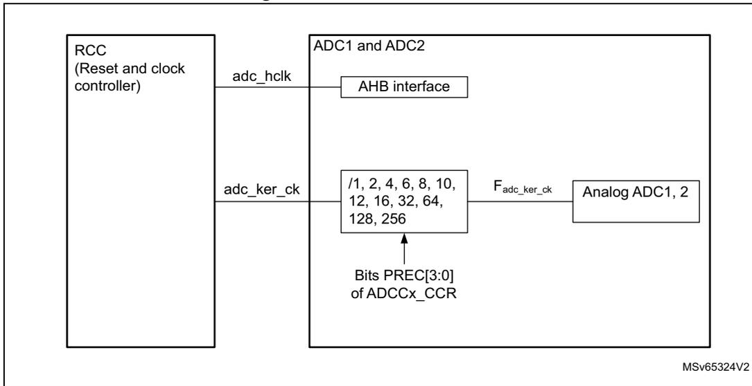
The diagram illustrates the clock architecture for the ADC. On the left, the RCC (Reset and clock controller) provides two clock signals:
adc_hclk
and
adc_ker_ck
. The
adc_hclk
signal is connected to the AHB interface within the ADC1 and ADC2 block. The
adc_ker_ck
signal is connected to a prescaler block labeled with values:
/1, 2, 4, 6, 8, 10, 12, 16, 32, 64, 128, 256
. This prescaler is controlled by the
Bits PREC[3:0] of ADCCx_CCR
. The output of the prescaler, labeled
F_adc_ker_ck
, is connected to the Analog ADC1, 2 block. The entire ADC section, including the AHB interface, prescaler, and analog ADCs, is contained within a larger block labeled
ADC1 and ADC2
. A reference code
MSV65324V2
is located in the bottom right corner of the diagram.
1. Refer to the RCC section for information on
adc_hclk
and
adc_ker_ck
generation.
Clock ratio constraint between ADC clock and AHB clock
There are generally no constraints to be respected for the ratio between the ADC clock and the AHB clock. However, the ratio must be carefully chosen to avoid any overrun especially if the clock AHB is much slower than the ADC clock.
33.4.4 ADC connectivity
Figure 223. ADC1 connectivity
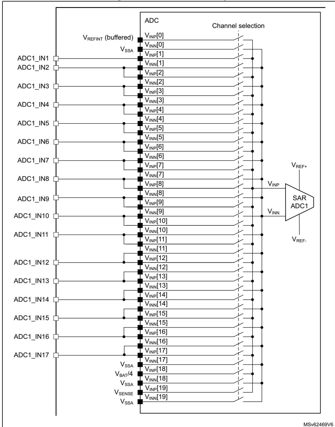
The diagram illustrates the internal connectivity of the ADC12. On the left, external pins are labeled ADC1_IN1 through ADC1_IN17. These are connected to a central column of internal signal nodes. The nodes are organized into pairs for each channel index i: V INP [i] and V INN [i].
- ADC1_IN1 connects to V INP [0].
- ADC1_IN2 connects to V INN [2].
- ADC1_IN3 connects to V INP [3].
- ADC1_IN4 connects to V INN [4].
- ADC1_IN5 connects to V INP [5].
- ADC1_IN6 connects to V INN [6].
- ADC1_IN7 connects to V INP [7].
- ADC1_IN8 connects to V INN [8].
- ADC1_IN9 connects to V INP [9].
- ADC1_IN10 connects to V INN [10].
- ADC1_IN11 connects to V INP [11].
- ADC1_IN12 connects to V INN [12].
- ADC1_IN13 connects to V INP [13].
- ADC1_IN14 connects to V INN [14].
- ADC1_IN15 connects to V INP [15].
- ADC1_IN16 connects to V INN [16].
- ADC1_IN17 connects to V INP [17].
Additional internal signal sources are connected to the central column:
- V REFINT (buffered) connects to V INP [0].
- V SSA connects to V INN [0] and V INN [1].
- V SSA connects to V INP [1].
- V SSA connects to V INN [2].
- V SSA connects to V INP [2].
- V SSA connects to V INN [3].
- V SSA connects to V INP [3].
- V SSA connects to V INN [4].
- V SSA connects to V INP [4].
- V SSA connects to V INN [5].
- V SSA connects to V INP [5].
- V SSA connects to V INN [6].
- V SSA connects to V INP [6].
- V SSA connects to V INN [7].
- V SSA connects to V INP [7].
- V SSA connects to V INN [8].
- V SSA connects to V INP [8].
- V SSA connects to V INN [9].
- V SSA connects to V INP [9].
- V SSA connects to V INN [10].
- V SSA connects to V INP [10].
- V SSA connects to V INN [11].
- V SSA connects to V INP [11].
- V SSA connects to V INN [12].
- V SSA connects to V INP [12].
- V SSA connects to V INN [13].
- V SSA connects to V INP [13].
- V SSA connects to V INN [14].
- V SSA connects to V INP [14].
- V SSA connects to V INN [15].
- V SSA connects to V INP [15].
- V SSA connects to V INN [16].
- V SSA connects to V INP [16].
- V SSA connects to V INN [17].
- V SSA connects to V INP [17].
- V BAT/4 connects to V INN [18].
- V SENSE connects to V INP [19].
- V SSA connects to V INN [19].
On the right, a 'Channel selection' matrix (indicated by a dashed vertical line) allows for the routing of these internal signals to the SAR ADC1 block. The SAR ADC1 block has inputs for V REF+ , V REF- , V INP , and V INN .
MSv62469V6
- 1. V INN [i] signal can only be used when the corresponding ADC input channel is configured as differential mode.
Figure 224. ADC2 connectivity (STM32U59x/5Ax/5Fx/5Gx)
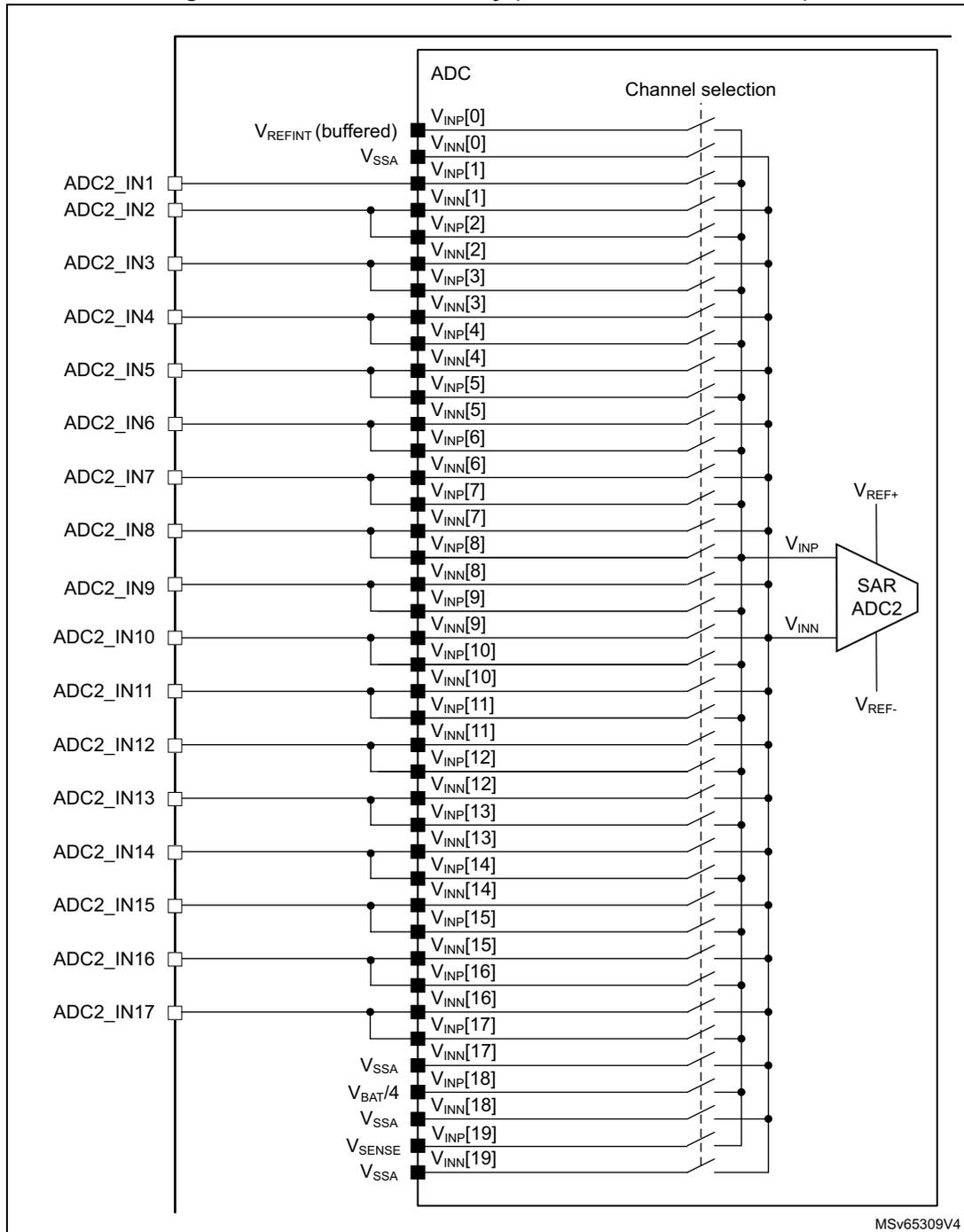
The diagram illustrates the connectivity of the ADC2 module. On the left, external pins are labeled from ADC2_IN1 to ADC2_IN17. These are connected to a central column of ADC pins labeled V_INP[0] through V_INP[19] and V_INN[0] through V_INN[19]. The connections are as follows:
- V_INP[0] and V_INN[0] are connected to V_REFINT (buffered).
- V_INP[1] and V_INN[1] are connected to ADC2_IN1.
- V_INP[2] and V_INN[2] are connected to ADC2_IN2.
- V_INP[3] and V_INN[3] are connected to ADC2_IN3.
- V_INP[4] and V_INN[4] are connected to ADC2_IN4.
- V_INP[5] and V_INN[5] are connected to ADC2_IN5.
- V_INP[6] and V_INN[6] are connected to ADC2_IN6.
- V_INP[7] and V_INN[7] are connected to ADC2_IN7.
- V_INP[8] and V_INN[8] are connected to ADC2_IN8.
- V_INP[9] and V_INN[9] are connected to ADC2_IN9.
- V_INP[10] and V_INN[10] are connected to ADC2_IN10.
- V_INP[11] and V_INN[11] are connected to ADC2_IN11.
- V_INP[12] and V_INN[12] are connected to ADC2_IN12.
- V_INP[13] and V_INN[13] are connected to ADC2_IN13.
- V_INP[14] and V_INN[14] are connected to ADC2_IN14.
- V_INP[15] and V_INN[15] are connected to ADC2_IN15.
- V_INP[16] and V_INN[16] are connected to ADC2_IN16.
- V_INP[17] and V_INN[17] are connected to ADC2_IN17.
- V_INP[18] and V_INN[18] are connected to V_BAT/4.
- V_INP[19] and V_INN[19] are connected to V_SENSE.
Additional pins V_SSA and V_REFINT (buffered) are also shown at the top and bottom of the central column. On the right, a block labeled 'SAR ADC2' receives V_INP and V_INN signals. It is connected to V_REF+ and V_REF- reference voltages. A 'Channel selection' block is shown above the SAR ADC2 block, with lines connecting it to the V_INP and V_INN pins.
MSv65309V4
33.4.5 Slave AHB interface
The ADC implements an AHB slave port for control/status register and data access. The features of the AHB interface are listed below:
- • Word (32-bit) accesses
- • Single cycle response
- • Response to all read/write accesses to the registers with zero wait states.
The AHB slave interface does not support split/retry requests and never generates AHB errors.
33.4.6 ADC Deep-power-down mode (DEEPPWD) and ADC voltage regulator (ADVREGEN)
By default, the ADC is in Deep-power-down mode where its supply voltage is internally switched off to reduce the leakage currents (the reset state of bit DEEPPWD is 1 in the ADC_CR register).
To start ADC operations, follow the sequence below:
- 1. First exit Deep-power-down mode by clearing the DEEPPWD bit.
- 2. Then, enable the ADC internal voltage regulator by setting the ADVREGEN bit in the ADC_CR register. The software must wait for the startup time of the ADC voltage regulator ( \( T_{ADCVREG\_STUP} \) ) before launching a calibration or enabling the ADC. This can be done by software by polling the LDORDY bit of the ADC_ISR register.
After ADC operations are complete, the ADC can be disabled (ADEN = 0). It is possible to save power by also disabling the ADC voltage regulator. This is done by clearing the ADVREGEN bit. Power consumption can be further reduced by reducing the leakage currents. In addition, it is possible to enter again in ADC Deep-power-down mode by setting DEEPPWD bit in ADC_CR register. This is particularly interesting before entering Stop mode.
Note: Setting DEEPPWD automatically disables the ADC voltage regulator and the ADVREGEN bit is automatically cleared.
When the internal voltage regulator is disabled (ADVREGEN = 0), the internal analog calibration factor is kept.
In ADC Deep-power-down mode (DEEPPWD = 1), the internal analog calibration is lost and it is necessary either to relaunch a calibration or apply again the calibration factor, which was previously saved (refer to Section 33.4.8: Calibration (ADCAL, ADCALLIN, ADC_CALFACT) ).
33.4.7 Single-ended and differential input channels
ADC channels can be configured either as single-ended input or as differential input. This is done by writing DIFSEL[19:0] bits in the ADC_DIFSEL register. This configuration must be performed while the ADC is disabled (ADEN = 0).
In single-ended input mode, the analog voltage to be converted for channel “i” is the difference between the external voltage \( V_{INP}[i] \) (positive input) and \( V_{REF-} \) (negative input).
In differential input mode, the analog voltage to be converted for channel “i” is the difference between the external voltage \( V_{INP}[i] \) (positive input) and \( V_{INN}[i] \) (negative input).
The output data in differential mode is an unsigned data:
- • When \( V_{INP}[i] = V_{REF+} \) : \( V_{INN}[i] = V_{REF+} \) and output data = 0x0000 (14-bit resolution mode),
- • When \( V_{INP}[i] = V_{REF+} \) : \( V_{INN}[i] = V_{REF-} \) and output data = 0x3FFF.
When ADC is configured as differential mode, both inputs must be biased at \( V_{REF+} / 2 \) voltage.
For a complete description of how the input channels are connected, refer to Section 33.4.4: ADC connectivity
Caution: When channel “i” is configured in differential input mode, its negative input voltage is connected to \( V_{INN}[i-1] \) .
33.4.8 Calibration (ADCAL, ADCALLIN, ADC_CALFACT)
The ADC provides an automatic calibration procedure that controls the whole calibration sequence including the ADC power-on/off. During the procedure, the ADC calculates an offset calibration factor for single-ended and differential mode. This factor includes the internal offset and the linearity that are applied internally to the ADC until the next ADC power-off. During the calibration procedure, the application must not use the ADC and must wait until the calibration is complete.
The calibration is a prerequisite to any ADC operation. It removes the systematic errors that may vary from chip to chip and enables to compensate offset and linearity deviation.
The offset calibration is the same for single-ended or differential channels.
The linearity correction must be done only once, regardless of single / differential configuration:
- • Set ADCALLIN in ADC_CR before launching a calibration that runs the linearity calibration simultaneously with the offset calibration or
- • Clear ADCALLIN in ADC_CR before launching a calibration that does not run the linearity calibration but only the offset calibration.
The calibration is then initiated by software by setting the ADCAL bit. The calibration can only be initiated when the ADC is disabled (ADEN = 0). ADCAL bit remains at 1 during all the calibration sequence. It is cleared by hardware as soon the calibration completes. At this time, the associated calibration factor is stored internally in the analog ADC.
The internal analog calibration is kept if the ADC is disabled (ADEN = 0). However, if the ADC is disabled for extended periods of time, the temperature changes, or the reference voltage is modified of more than 10%, it is recommended that a new offset calibration cycle is run before enabling the ADC again.
The internal analog calibration is lost each time the ADC power is switched off (for example, when the device enters Standby or \( V_{BAT} \) mode). In this case, to avoid spending time recalibrating the ADC, the calibration factor can be written again to the ADC analog block without recalibrating, assuming that the software has previously saved the calibration factor generated during the previous calibration.
The calibration factor can be written if the ADC is enabled and no calibration is ongoing (ADEN = 1 and ADSTART = 0 and JADSTART = 0). Then, at the next start of conversion, the calibration factor is injected into the analog ADC.
Refer to the device datasheet for the offset and linearity calibration time requirements.
Software procedure to calibrate the ADC
- 1. Make sure DEEPPWD = 0, ADVREGEN = 1 and check that the ADC voltage regulator startup time has elapsed (LDORDY = 1).
- 2. Make sure ADEN = 0.
- 3. Either enable the linearity calibration (ADCALLIN = 1) or disable it (ADCALLIN = 0).
- 4. Make sure CAPTURE_COEF and LATCH_COEF in ADC_CALFACT are cleared.
- 5. Set ADCAL in the ADC_CR register and wait until ADCAL = 0.
Figure 225 shows the ADC calibration timing diagram.
Note: The software can launch the calibration only when ADEN = 0, LDORDY = 1 (ADC disabled and LDO ready), and DUAL[4:0] = 0b00000.
Single-ended and differential channels cannot be calibrated separately. The offset calibration is performed within the same sequence.
Figure 225. ADC calibration
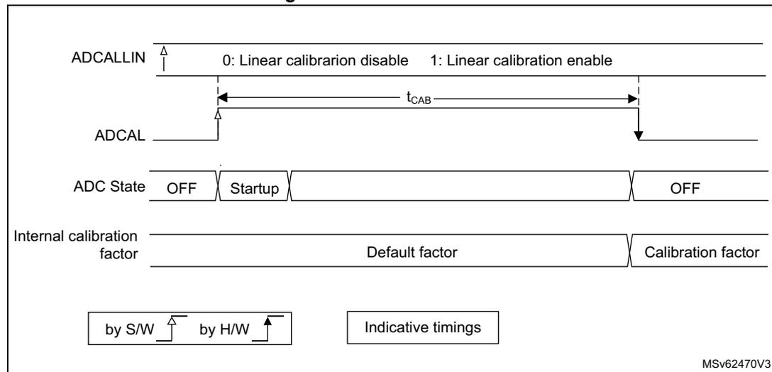
The diagram illustrates the timing sequence for ADC calibration across four horizontal timelines:
- ADCALLIN: Shows a transition from 0 (Linear calibration disable) to 1 (Linear calibration enable). The transition is triggered by software (S/W).
- ADCAL: Shows a transition from 1 to 0. The transition is triggered by hardware (H/W) and occurs after the ADCALLIN transition.
- ADC State: Shows the state of the ADC. It starts in OFF, transitions to Startup when ADCALLIN goes high, and returns to OFF when ADCAL goes low.
- Internal calibration factor: Shows the calibration factor being updated from the Default factor to the Calibration factor when ADCAL goes low.
A horizontal double-headed arrow labeled \( t_{CAB} \) indicates the time interval between the rising edge of ADCALLIN and the falling edge of ADCAL. A legend at the bottom indicates that transitions marked with an upward arrow are "by S/W" and those with a rightward arrow are "by H/W". The text "Indicative timings" is also present. The diagram is identified by the code MSV62470V3.
Reading calibration factor procedure
Once the calibration is complete (ADCAL bit cleared by hardware), the calibration factor can be read from the ADC_CALFACT2 register. The CALINDEX[0:3] bitfield of the ADC_CR register can be incremented to access other calibration factors:
- 1. Make sure DEEPPWD = 0, ADVREGEN = 1, and check that the ADC voltage regulator startup time has elapsed (LDORDY = 1).
- 2. Make sure that ADEN = 1.
- 3. Set CAPTURE_COEF and clear LATCH_COEF in the ADC_CALFACT register.
- 4. Select the calibration factor by setting CALINDEX[0:3] in ADC control register (ADC_CR) .
- 5. Read the calibration factor from the ADC_CALFACT2 register.
- 6. Repeat steps 4 and 5 for each required calibration factor.
- 7. Clear the CAPTURE_COEF bit in the ADC_CALFACT register.
Note: The software can access the calibration factor only when ADEN = 1, ADSTART = 0 and JADSTART = 0 (ADC enabled and no conversion is ongoing).
Software procedure to reinject the calibration factor into the ADC
- 1. Make sure ADEN = 1, ADSTART = 0 and JADSTART = 0 (ADC enabled and no conversion is ongoing).
- 2. Clear the CAPTURE_COEF and LATCH_COEF bits in the ADC_CALFACT register
- 3. Set CALINDEX[3:0] to the targeted calibration index to be updated, then write the calibration factor to CALFACT[31:0] in the ADC_CALFACT2 register.
- 4. Repeat step 3 for all the calibration index bytes.
- 5. Set the LATCH_COEF bit in the ADC_CALFACT register.
- 6. Clear the LATCH_COEF bit in the ADC_CALFACT register.
Note: The software is allowed to update the calibration factor only when ADEN = 1 and ADSTART = 0 and JADSTART = 0 (ADC enabled and no conversion is ongoing).
If some of the calibration factor bytes are not written when the LATCH_COEF bit is set, the calibration factor becomes the default value.
Calibration factor index
The calibration factors are stored in the analog block in an indexed way. Index 0b0000 and 0b1000 contain the offset calibration factor while index 0b0001 to 0b0110 contain the linearity factor. The lower two bytes of index 0b0111 contain the linearity calibration factor. The internal offset calibration factor must be programmed into byte 2 of index (0b0111). However, it is read at byte 3 of index 0b1000. When programming or reinjecting the calibration factor, make sure to use the correct indexes for read and write operations.
Refer to Table 309 for a summary.
Table 309. Calibration factor index
| CALINDEX[3:0] values | Calibration factor | Reset value | |||
|---|---|---|---|---|---|
| Byte location | |||||
| Byte 3 | Byte 2 | Byte 1 | Byte 0 | ||
| 0b0000 | Differential offset | Single-end offset | 0x036D 0648 | ||
| 0b0001 | Linearity factor 1 | 0x0004 0000 | |||
| 0b0010 | Linearity factor 2 | 0x0000 0200 | |||
| 0b0011 | Linearity factor 3 | 0x0080 0001 | |||
| 0b0100 | Linearity factor 4 | 0x2000 4000 | |||
| 0b0101 | Linearity factor 5 | 0x09EB 13D6 | |||
| 0b0110 | Linearity factor 6 | 0x027A 04F5 | |||
| 0b0111 (read) | Reserved | Reserved | Linearity factor 7 | 0x8000 016A | |
| 0b0111 (write) | Reserved | Internal offset | |||
| 0b1000 (read) | Internal offset | Reserved | Reserved | Reserved | 0x8C02 7A00 |
| 0b1001 | Reserved | Calibration mode | Reserved | Reserved | 0x3000 1100 |
| 0b1000 (write) | Reserved | Reserved | Reserved | Reserved | - |
| Other values | Reserved | - | |||
When the calibration factor is latched, all the index bytes must be uploaded, otherwise the non-uploaded index bytes are reset to their default value.
Extended calibration mode
To enhance the ADC performance, the extended calibration mode is implemented on some product versions (see Section 33.3: ADC implementation ).
Below the procedure to enable the extended calibration mode:
- 1. Make sure that DEEPPWD = 0 and ADVREGEN = 1, and check that the ADC voltage regulator startup time has elapsed (LDORDY = 1).
- 2. Set ADCALLIN in the ADC_CR register.
- 3. Make sure CAPTURE_COEF and LATCH_COEF of ADC_CALFACT are cleared.
- 4. Set ADEN and wait until ADRDY is set.
- 5. Set CALINDEX[3:0] = 0b1001, then write CALFACT[31:0] = 0x0302 1100 in the ADC_CALFACT2 register.
- 6. Set the LATCH_COEF bit in the ADC_CALFACT register.
- 7. Set the ADDIS and wait until the ADEN bit is cleared.
- 8. Set the ADCAL in the ADC_CR register and wait until ADCAL bit is cleared.
Note: Once the calibration is complete, the value of CALFACT[31:0] at CALINDEX[3:0] = 0b1001 is reset.
The values written to the ADC_CR (CALINDEX[3:0] and ADCALLIN), ADC_CALFACT, and ADC_CALFACT2 registers are internally applied asynchronously from \( F_{adc\_ker\_ck} \) . As a result, consecutive fast accesses to these registers might generate errors. To prevent errors
from occurring, the software can insert the
__DMB();
command after each access to these registers.
To run the calibration, set DUAL[4:0] = 0b00000.
33.4.9 ADC on-off control (ADEN, ADDIS, ADRDY)
First of all, follow the procedure described in Section 33.4.6: ADC Deep-power-down mode (DEEPPWD) and ADC voltage regulator (ADVREGEN) .
Once the DEEPPWD bit is cleared and the ADVREGEN bit is set, the ADC can be enabled. It requires a stabilization time of \( t_{STAB} \) before staring converting accurately (see Figure 226 ). Two control bits enable or disable the ADC:
- • When ADEN = 1: the ADC is enabled. The ADRDY is set as soon as the ADC is ready for operation.
- • When ADDIS = 1: the ADC is disabled.
ADEN and ADDIS bits are automatically cleared by hardware as soon as the analog ADC is effectively disabled.
Regular conversions can then start either by setting ADSTART (refer to Section 33.4.19: Conversion on external trigger and trigger polarity (EXTSEL, EXTEN[1:0], JEXTSEL, JEXTEN[1:0]) ) or when an external trigger event occurs if triggers are enabled.
Injected conversions start by setting JADSTART or when an external injected trigger event occurs if injected triggers are enabled.
Software procedure to enable the ADC
- 1. Clear the ADRDY bit in the ADC_ISR register by writing 1.
- 2. Set ADEN = 1.
- 3. Wait until ADRDY = 1 (ADRDY is set after the ADC startup time). This can be done by using the associated interrupt (ADRDYIE = 1).
- 4. Clear the ADRDY bit in the ADC_ISR register by writing 1 (optional).
Software procedure to disable the ADC
- 1. Check that both ADSTART = 0 and JADSTART = 0 to make sure that no conversion is ongoing. If required, stop any ongoing regular and injected conversion by setting ADSTP = 1 and JADSTP = 1 and then wait until ADSTP = 0 and JADSTP = 0.
- 2. Set ADDIS.
- 3. If required by the application, wait until ADEN = 0, until the analog ADC is effectively disabled (ADDIS is automatically reset once ADEN = 0).
Figure 226. Enabling/disabling the ADC
MSv62472V1
33.4.10 Constraints when writing the ADC control bits
The software can program the RCC control bits to configure and enable the ADC clock (refer to the Reset and clock control section), the control DIFSEL bits in the ADC_DIFSEL register, the ADC12_CCR register and the ADCAL and ADEN control bits in the ADC_CR register, only if the ADC is disabled.
The software can program the ADCAL bit to launch the calibration when ADEN is cleared. It can read or update the calibration factor if ADEN is set and no conversion is ongoing (ADSTART and JADSTART both cleared).
The software is then allowed to write the ADSTART, JADSTART, and ADDIS control bits in the ADC_CR register only if the ADC is enabled and there is no pending request to disable it (ADEN must be equal to 1 and ADDIS to 0).
The following constraints apply to all the other control bits of the ADC_CFGRx, ADC_SMPRy, ADC_LTRy, ADC_HTRy, ADC_SQRY, ADC_OFRy and ADC_IER registers:
- • Control bits related to configuration of regular conversions: the software is allowed to write them only if the ADC is enabled (ADEN = 1) and no regular conversion is ongoing (ADSTART must be equal to 0).
- • Control bits related to configuration of injected conversions: the software is allowed to write them only if the ADC is enabled (ADEN = 1) and no injected conversion is ongoing (JADSTART must be equal to 0).
- • ADC_LTRy, ADC_HTRy registers can be modified when an analog-to-digital conversion is ongoing (refer to Section 33.4.29: Analog window watchdog (AWD1EN, JAWD1EN, AWD1SGL, AWD1CH, AWD2CH, AWD3CH, AWD_HTRy, AWD_LTRy, AWBy) for details).
The software can write ADSTP or JADSTP control bits in the ADC_CR register only if the ADC is enabled, a conversion is ongoing and there is no pending request to disable it (ADSTART or JADSTART must be equal to 1 and ADDIS to 0).
Note: There is no hardware protection to prevent these forbidden write accesses that may cause the ADC to enter an unknown state. To recover from this situation, the ADC must be disabled (clear ADEN as well as all the bits of the ADC_CR register).
33.4.11 Channel selection (SQRx, JSQRx)
The ADC features up to 20 multiplexed channels per ADC:
- • Up to 17 analog inputs coming from GPIO pads
- • Each ADC is connected to 3 internal analog inputs:
- – the internal temperature sensor ( \( V_{\text{SENSE}} \) )
- – the internal reference voltage ( \( V_{\text{REFINT}} \) )
- – the \( V_{\text{BAT}} \) monitoring channel ( \( V_{\text{BAT}}/4 \) )
Refer to Table ADC interconnection in Section 33.4.2: ADC pins and internal signals for the connection of the above internal analog inputs to external ADC pins or internal signals.
The conversions can be organized in two groups: regular and injected. A group consists of a sequence of conversions that can be done on any channel and in any order. For instance, it is possible to implement the conversion sequence in the following order: ADC_IN3, ADC_IN8, ADC_IN2, ADC_IN2, ADC_IN0, ADC_IN2, ADC_IN2, ADC_IN15.
- • A regular group is composed of up to 16 conversions. The regular channels and their order in the conversion sequence must be selected in the ADC_SQRy registers. The total number of conversions in the regular group must be written in the L[3:0] bits in the ADC_SQR1 register.
- • An injected group is composed of up to four conversions. The injected channels and their order in the conversion sequence must be selected in the ADC_JSQR register. The total number of conversions in the injected group must be written in the L[1:0] bits in the ADC_JSQR register.
ADC_SQRy registers must not be modified while regular conversions are ongoing. To modify ADC_SQRy registers, the ADC regular conversions must first be stopped by setting ADSTP (refer to Section 33.4.18: Stopping an ongoing conversion (ADSTP, JADSTP) ).
Note: To convert one of the internal analog channels, the corresponding analog sources must first be enabled by programming VBATEN, VSENSESEL, or VREFEN bits in the ADC12_CCR registers.
33.4.12 Channel preselection register (ADC_PCSEL)
For each channel selected through SQRx or JSQRx bits, the corresponding ADC_PCSEL bit must be configured in advance.
This ADC_PCSEL bit controls the analog switch integrated in the I/O level. The ADC input multiplexer selects the ADC input according to SQRx and JSQRx configuration with very high speed and the analog switch integrated in the I/O cannot react as fast as the ADC multiplexer does. To avoid the delay due to on analog switch control on the I/O, it is necessary to preselect the input channels that are selected through the SQRx and JSQRx. The selection is based on the \( V_{\text{INP}}[i] \) of each ADC input. For example, if the ADC converts ADC_IN1, the PCSEL1 bit must also be set in ADC_PCSEL.
33.4.13 Channel-wise programmable sampling time (SMPR1, SMPR2)
Before starting a conversion, the ADC must establish a direct connection between the voltage source under measurement and the embedded sampling capacitor of the ADC. This sampling time must be enough for the input voltage source to charge the embedded capacitor to the input voltage level.
Each channel can be sampled with a different sampling time that is programmable using the SMP[2:0] bits in the ADC_SMPR1 and ADC_SMPR2 registers. It is therefore possible to select among the following sampling time values:
- • SMP = 000: 5 ADC clock cycles
- • SMP = 001: 6 ADC clock cycles
- • SMP = 010: 12 ADC clock cycles
- • SMP = 011: 20 ADC clock cycles
- • SMP = 100: 36 ADC clock cycles
- • SMP = 101: 68 ADC clock cycles
- • SMP = 110: 391 ADC clock cycles
- • SMP = 111: 814 ADC clock cycles
The total conversion time is calculated as follows:
Example
When converting a single data, the sampling time is five cycles and the conversion time is 17 cycles for 14-bit mode. With an \( F_{\text{adc\_ker\_ck}} \) of 55 MHz:
The above result assumes that \( R_{\text{AIN}} \ll 1 \text{ K}\Omega \) (refer to the datasheet for additional sampling time to be added depending on the external resistance).
The ADC notifies the end of the sampling phase by setting the status bit EOSMP (only for regular conversion).
I/O analog switch voltage booster
The resistance of the I/O analog switches increases when the \( V_{\text{DDA}} \) voltage is too low. The sampling time must consequently be adapted accordingly (refer to the device datasheet for the corresponding electrical characteristics). This resistance can be minimized at low \( V_{\text{DDA}} \) voltage by enabling an internal voltage booster (refer to the SYSCFG section for more details).
Bulb sampling mode
When the BULB bit is set in the ADC_CFGR2 register, the sampling period starts immediately after the last ADC conversion. A hardware or software trigger starts the conversion after the sampling time has been programmed in the ADC_SMPR1 register. The very first ADC conversion, after the ADC is enabled, is performed with the sampling time programmed in SMP bits. The bulb mode is effective starting from the second conversion.
The maximum sampling time is limited (refer to the ADC characteristics section of the datasheet).
The bulb mode may not be used in continuous conversion mode or with injected channel conversion.
When the BULB bit is set, it is not allowed to set the SMPTRIG bit in ADC_CFGR2.
When conversions in bulb mode are stopped by setting ADSTP bit or when the DMA transfers are complete, the ADC must be disabled by setting ADDIS bit.
Figure 227. Bulb mode timing diagram
The figure is a timing diagram for the ADC12 Bulb mode. It is divided into two horizontal sections. The top section, 'Normal mode (discontinuous sampling)', shows the 'ADC state' as a sequence of 'idle', 'sample', and 'conversion' periods. The 'Trigger' signal is shown as a series of pulses. The bottom section, 'BULB mode (continuous sampling)', shows the 'ADC state' as 'idle', 'sample', 'conversion', 'sample', 'conversion', and 'sample'. The 'Trigger' signal is shown as a pulse that starts the sampling period and a falling edge that ends it. A double-headed arrow indicates the 'Sampling time programmed in SMP bits' between the rising and falling edges of the trigger signal. The diagram is labeled 'MSV62473V1' in the bottom right corner.
Sampling time control trigger mode
When the SMPTRIG bit is set, the sampling time programmed through SMPx bits is not applicable. The sampling time is controlled by the trigger signal edge.
When a hardware trigger is selected, each rising edge of the trigger signal starts the sampling period. A falling edge ends the sampling period and starts the conversion.
When a software trigger is selected, the software trigger is not the ADSTART bit in ADC_CR but the SWTRIG bit. SWTRIG bit has to be set to start the sampling period, and the SWTRIG bit has to be cleared to end the sampling period and start the conversion.
The maximum sampling time is limited (refer to the ADC characteristics section of the datasheet).
This mode is not compatible with the continuous conversion mode and injected channel conversion.
When the SMPTRIG bit is set, it is not allowed to set the BULB bit.
33.4.14 Single conversion mode (CONT = 0)
In single conversion mode, the ADC performs once the conversions of all channels. This mode is started with the CONT bit at 0 by either:
- • Setting the ADSTART bit in the ADC_CR register (for a regular channel, with software trigger selected)
- • Setting the JADSTART bit in the ADC_CR register (for an injected channel, with software trigger selected)
- • External hardware trigger event (for a regular or injected channel)
ADSTART bit or JADSTART bit must be set before triggering an external event.
Inside the regular sequence, after each conversion is complete:
- • The converted data are stored into the 32-bit ADC_DR register
- • The EOC (end of regular conversion) flag is set
- • An interrupt is generated if the EOCIE bit is set
Inside the injected sequence, after each conversion is complete:
- • The converted data are stored into one of the four 32-bit ADC_JDRy registers
- • The JEOC (end of injected conversion) flag is set
- • An interrupt is generated if the JEOCIE bit is set
After the regular sequence is complete:
- • The EOS (end of regular sequence) flag is set
- • An interrupt is generated if the EOSIE bit is set
After the injected sequence is complete:
- • The JEOS (end of injected sequence) flag is set
- • An interrupt is generated if the JEOSIE bit is set
Then the ADC stops until a new external regular or injected trigger occurs or until bit ADSTART or JADSTART is set again.
Note: To convert a single channel, program a sequence with a length of 1.
33.4.15 Continuous conversion mode (CONT = 1)
This mode applies to regular channels only.
In continuous conversion mode, when a software or hardware regular trigger event occurs, the ADC performs once all the regular conversions of the channels and then automatically restarts and continuously converts each conversion of the sequence. This mode is started with the CONT bit at 1 either by an external trigger or by setting the ADSTART bit in the ADC_CR register.
Inside the regular sequence, after each conversion is complete:
- • The converted data are stored into the 32-bit ADC_DR register
- • The EOC (end of conversion) flag is set
- • An interrupt is generated if the EOCIE bit is set
After the sequence of conversions is complete:
- • The EOS (end of sequence) flag is set
- • An interrupt is generated if the EOSIE bit is set
Then, a new sequence restarts immediately and the ADC continuously repeats the conversion sequence.
Note: To convert a single channel, program a sequence with a length of 1.
It is not possible to have both discontinuous mode and continuous mode enabled: it is forbidden to set both DISCEN = 1 and CONT = 1.
Injected channels cannot be converted continuously. The only exception is when an injected channel is configured to be converted automatically after regular channels in continuous mode (using the JAUTO bit), refer to Section : Auto-injection mode ).
33.4.16 Starting conversions (ADSTART, JADSTART)
The software starts ADC regular conversions by setting ADSTART. When ADSTART is set, the conversion starts:
- • immediately if EXTEN[1:0] = 0x0 (software trigger) or
- • at the next active edge of the selected regular hardware trigger, if EXTEN[1:0] is not equal to 0x0
The software starts ADC injected conversions by setting JADSTART. When JADSTART is set, the conversion starts:
- • immediately, if JEXTEN[1:0] = 0x0 (software trigger) or
- • at the next active edge of the selected injected hardware trigger if JEXTEN[1:0] is not equal to 0x0
Note: In auto-injection mode (JAUTO = 1), use the ADSTART bit to start regular conversions followed by auto-injected conversions (JADSTART must be kept cleared).
ADSTART and JADSTART also provide information on whether any ADC operation is ongoing. The ADC can be reconfigured while ADSTART and JADSTART are both cleared (the ADC is idle).
ADSTART is cleared by hardware:
- • In single mode with software trigger (CONT = 0, EXTEN[1:0] = 0x0): at any end of the conversion sequence (EOS = 1)
- • In discontinuous mode with software trigger (CONT = 0, DISCEN = 1, EXTEN[1:0] = 0x0): at end of conversion (EOC = 1)
- • In all other cases (CONT = x, EXTEN[1:0] = x): after executing the ADSTP assertion procedure by software.
Note: In continuous mode (CONT = 1), ADSTART is not cleared by hardware with the assertion of EOS because the sequence is automatically relaunched.
When a hardware trigger is selected in single mode (CONT = 0 and EXTEN[1:0] ≠ 0x0), ADSTART is not cleared by hardware with the assertion of EOS to help the software that does not need to reset ADSTART again for the next hardware trigger event. This ensures that no further hardware triggers are missed.
JADSTART is cleared by hardware:
- • In single mode with software injected trigger (JEXTEN[1:0] = 0x0): at any end of the injected conversion sequence (JEOS assertion) or at any end of subgroup processing if JDISCEN = 1
- • In all other cases (JEXTEN[1:0]=x): after executing the JADSTP assertion procedure by software.
Note: When the software trigger is selected, the ADSTART bit must not be set if the EOC flag is still high.
33.4.17 Timing
The elapsed time between the start of a conversion and the end of conversion is the sum of the configured sampling time plus the successive approximation time depending on data resolution for single conversion and minus the overlap time between the sampling and the previous SAR for continuous conversion.
In single conversion mode:
Figure 228. Analog-to-digital conversion time in single conversion
The diagram shows the timing of signals during a single conversion. The ADC state starts at RDY, then goes to Sampling Ch(N) for a duration of \( t_{\text{SMPL}}^{(1)} \) , then to Converting Ch(N) for a duration of \( t_{\text{SAR}}^{(2)} \) , and finally to Sampling Ch(N+1). The Analog channel is Ch(N) during sampling and conversion, and Ch(N+1) during the next sampling. The Internal S/H is Sample AIN(N) during sampling and Hold AIN(N) during conversion, then Sample AIN(N+1) during the next sampling. ADSTART is set by SW at the beginning of sampling. EOSMP is set by HW at the end of sampling and cleared by SW at the end of conversion. EOC is set by HW at the end of conversion and cleared by HW/SW. ADC_DR contains Data N-1 during conversion and Data N after conversion. Indicative timings are shown for \( t_{\text{SMPL}}^{(1)} \) and \( t_{\text{SAR}}^{(2)} \) . MSV30532V2
1. \( t_{\text{SMPL}} \) depends on SMP[2:0].
2. \( t_{\text{SAR}} \) depends on RES[1:0].
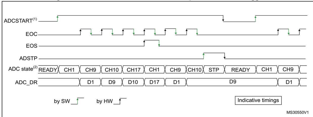
33.4.18 Stopping an ongoing conversion (ADSTP, JADSTP)
The software can decide to stop regular conversions ongoing by setting ADSTP, and injected conversions ongoing by setting JADSTP.
Stopping conversions resets the ongoing ADC operation. The ADC can then be reconfigured (for example by changing the channel selection or the trigger). It is then ready for a new operation.
Injected conversions can be stopped while regular conversions are still ongoing and vice versa. This enables, for instance, to reconfigure the injected conversion sequence and triggers while regular conversions are still ongoing (and vice versa).
When the ADSTP bit is set by software, any ongoing regular conversion is aborted with partial result discarded (ADC_DR register is not updated with the current conversion).
When the JADSTP bit is set by software, any ongoing injected conversion is aborted with partial result discarded (ADC_JDRy register is not updated with the current conversion). The scan sequence is also aborted and reset (meaning that relaunching the ADC would restart a new sequence).
Once this procedure is complete, ADSTP/ADSTART bits (in case of regular conversion), or JADSTP/JADSTART bits (in case of injected conversion) are cleared by hardware. The software must poll ADSTART (or JADSTART) until the bit is reset before assuming the ADC is completely stopped.
Note: In auto-injection mode (JAUTO = 1), setting the ADSTP bit aborts both regular and injected conversions (JADSTP must not be used).
Figure 229. Stopping ongoing regular conversions
This timing diagram illustrates the sequence of events for stopping ongoing regular conversions. The top line shows the ADC state transitioning from RDY to Sample Ch(N-1) upon a Trigger, then to Convert Ch(N-1), back to RDY, then to Sample Ch(N) upon another Trigger, then to C, and finally back to RDY. The ADSTART bit is set by software (SW) to initiate regular conversions and is cleared by hardware (HW) when the ADC returns to the RDY state. A note indicates that software cannot configure regular conversion selection and triggers. The ADSTP bit is set by software to stop conversions and is cleared by hardware. The ADC_DR register contains Data N-2 and Data N-1.
MSV62490V1
Figure 230. Stopping ongoing regular and injected conversions
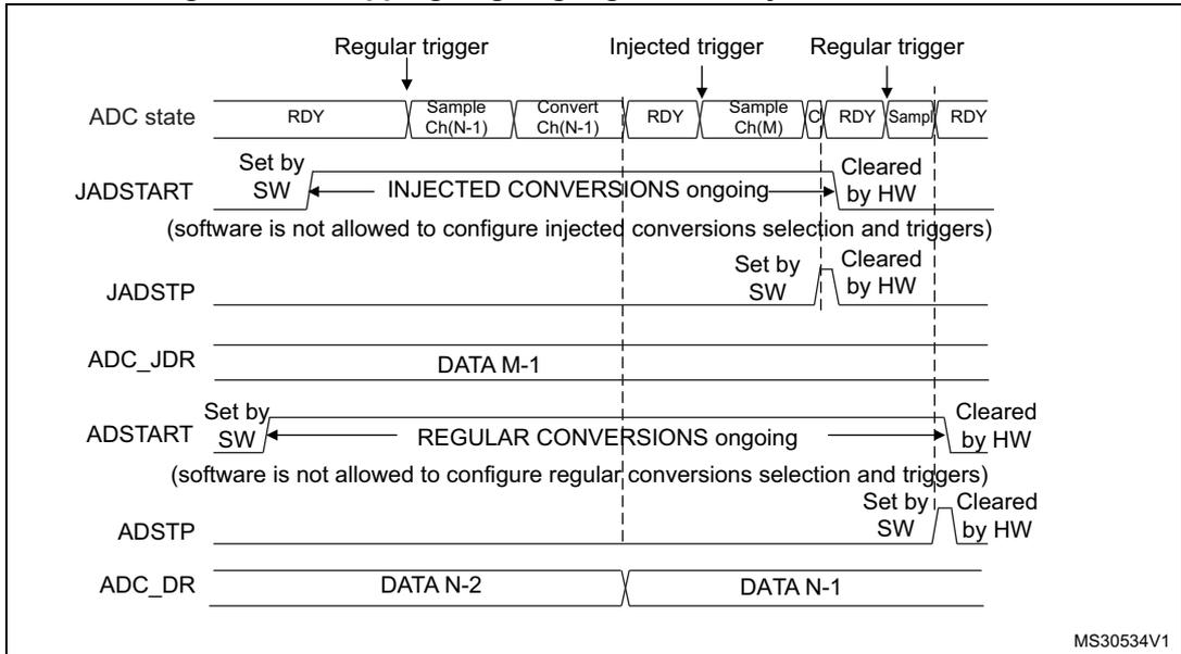
This timing diagram shows the sequence of events for stopping ongoing regular and injected conversions. The ADC state transitions are triggered by Regular, Injected, and Regular triggers. The JADSTART bit is set by software to start injected conversions and is cleared by hardware. A note indicates that software cannot configure injected conversion selection and triggers. The JADSTP bit is set by software to stop injected conversions and is cleared by hardware. The ADSTART bit is set by software to start regular conversions and is cleared by hardware. A note indicates that software cannot configure regular conversion selection and triggers. The ADSTP bit is set by software to stop regular conversions and is cleared by hardware. The ADC_JDR register contains DATA M-1, and the ADC_DR register contains DATA N-2 and DATA N-1.
MS30534V1
33.4.19 Conversion on external trigger and trigger polarity (EXTSEL, EXTEN[1:0], JEXTSEL, JEXTEN[1:0])
A conversion or a sequence of conversions can be triggered either by software or by an external event (for example, timer capture, input pins). If the EXTEN[1:0] control bits (for a regular conversion) or JEXTEN[1:0] bits (for an injected conversion) are different from 00, then external events are able to trigger a conversion with the selected polarity.
The regular trigger selection is effective once software has set bit ADSTART = 1 and the injected trigger selection is effective once software has set bit JADSTART = 1.
Any hardware trigger which occurs while a conversion is ongoing are ignored.
- • If ADSTART = 0, regular hardware triggers are ignored.
- • If JADSTART = 0, injected hardware triggers are ignored.
Table 310 provides the correspondence between the EXTEN[1:0] and JEXTEN[1:0] values and the trigger polarity.
Table 310. Configuring the trigger polarity for regular external triggers
| EXTEN[1:0] | Source |
|---|---|
| 00 | Hardware Trigger detection disabled, software trigger detection enabled |
| 01 | Hardware Trigger with detection on the rising edge |
| 10 | Hardware Trigger with detection on the falling edge |
| 11 | Hardware Trigger with detection on both the rising and falling edges |
Note: The polarity of the regular trigger cannot be changed on-the-fly.
Table 311. Configuring the trigger polarity for injected external triggers
| JEXTEN[1:0] | Source |
|---|---|
| 00 | Hardware trigger detection disabled, software trigger detection enabled |
| 01 | Hardware trigger with detection on the rising edge |
| 10 | Hardware trigger with detection on the falling edge |
| 11 | Hardware trigger with detection on both the rising and falling edges |
The EXTSEL[4:0] and JEXTSEL[4:0] control bits select which events can trigger regular and injected groups conversion, out of 21 possibilities.
A regular group conversion can be interrupted by an injected trigger.
Note: The trigger selection cannot be changed on-the-fly.
Figure 231. Triggers are shared between ADC master and ADC slave
![Schematic diagram showing trigger connections between ADC MASTER and ADC SLAVE. The diagram illustrates how external triggers (adc_ext0_trg, adc_ext1_trg, adc_ext31_trg) and JEXTI triggers (adc_jext0_trg, adc_jext1_trg, adc_jext31_trg) are shared between the master and slave ADC units. Each ADC unit has its own multiplexers for regular and injected triggers, controlled by EXTSEL[4:0] and JEXTSEL[4:0] registers. The diagram is labeled MSV41035V2.](/RM0456-STM32U5/9deeda16d37bfbc5d6e1f9062fe82754_img.jpg)
Refer to Table ADC external triggers for regular channels and Table ADC external triggers for injected channels in Section 33.4.2: ADC pins and internal signals for the connection of the above internal analog inputs to external ADC pins or internal signals.
33.4.20 Injected channel management
Triggered injection mode
To use triggered injection, the JAUTO bit must be cleared in the ADC_CFGR1 register:
- 1. Start the conversion of a group of regular channels either by an external trigger or by setting the ADSTART bit in the ADC_CR register.
- 2. If an external injected trigger occurs or if the JADSTART bit in the ADC_CR register is set during the conversion of a regular group of channels, the current conversion is reset and the injected channel sequence switches are launched (all the injected channels are converted once).
- 3. Then, the regular conversion of the regular group of channels is resumed from the last interrupted regular conversion.
- 4. If a regular event occurs during an injected conversion, the injected conversion is not interrupted but the regular sequence is executed at the end of the injected sequence. Figure 232 shows the corresponding timing diagram.
Note: When using triggered injection, one must ensure that the interval between trigger events is longer than the injection sequence. For instance, if the sequence length is 44 ADC clock cycles (that is two conversions with a minimum sampling time), the minimum interval between triggers must be 45 ADC clock cycles.
Auto-injection mode
If the JAUTO bit is set in the ADC_CFGR1 register, the channels in the injected group are automatically converted after the regular group of channels. This can be used to convert a sequence of up to 20 conversions programmed in the ADC_SQRy and ADC_JSQR registers.
In this mode, the ADSTART bit in the ADC_CR register must be set to start regular conversions, followed by injected conversions (JADSTART must be kept cleared). Setting the ADSTP bit aborts both regular and injected conversions (JADSTP bit must not be used).
In this mode, the external trigger on injected channels must be disabled.
If the CONT bit is also set in addition to the JAUTO bit, regular channels followed by injected channels are continuously converted.
Note: It is not possible to use both the auto-injected and discontinuous modes simultaneously.
When the DMA is used for exporting the regular sequencer's data in JAUTO mode, it is necessary to program it in circular mode (CIRC bit set in the DMA_CCRx register). If the CIRC bit is reset (single-shot mode), the JAUTO sequence is stopped upon a DMA Transfer Complete event.
Figure 232. Injected conversion latency
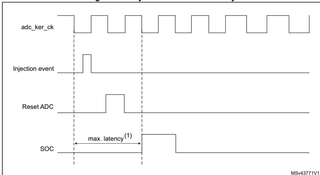
The figure is a timing diagram illustrating the injected conversion latency. It shows four signal traces over time:
- adc_ker_ck : A periodic square wave representing the ADC kernel clock.
- Injection event : A short pulse that triggers the injected conversion sequence.
- Reset ADC : A pulse that goes high following the injection event and then goes low.
- SOC : A pulse that goes high when the Reset ADC signal goes low and then goes low when the adc_ker_ck signal goes high.
- 1. The maximum latency value can be found in the electrical characteristics of the device datasheet.
33.4.21 Discontinuous mode (DISCEN, DISCNUM, JDISCEN)
Regular group mode
This mode is enabled by setting the DISCEN bit in the ADC_CFGR1 register.
It is used to convert a short sequence (subgroup) of n conversions ( \( n \leq 8 \) ) that is part of the sequence of conversions selected in the ADC_SQRy registers. The value of n is specified by writing to the DISCNUM[2:0] bits in the ADC_CFGR1 register.
When an external trigger occurs, it starts the next n conversions selected in the ADC_SQRx registers until all the conversions in the sequence are done. The total sequence length is defined by the L[3:0] bits in the ADC_SQR1 register.
Example
- • DISCEN = 1, n=3, channels to be converted = 1, 2, 3, 6, 7, 8, 9, 10, 11
- – 1st trigger: channels converted are 1, 2, 3 (an EOC event is generated at each conversion).
- – 2nd trigger: channels converted are 6, 7, 8 (an EOC event is generated at each conversion).
- – 3rd trigger: channels converted are 9, 10, 11 (an EOC event is generated at each conversion) and an EOS event is generated after the conversion of channel 11.
- – 4th trigger: channels converted are 1, 2, 3 (an EOC event is generated at each conversion).
- – ...
- • DISCEN = 0, channels to be converted = 1, 2, 3, 6, 7, 8, 9, 10, 11
- – First trigger: the complete sequence is converted: channel 1, then 2, 3, 6, 7, 8, 9, 10 and 11. Each conversion generates an EOC event and the last one also generates an EOS event.
- – All the next trigger events relaunch the complete sequence.
Note: When a regular group is converted in discontinuous mode, no rollover occurs (the last subgroup of the sequence can have less than n conversions).
When all subgroups are converted, the next trigger starts the conversion of the first subgroup. In the example above, the 4th trigger reconverts the channels 1, 2 and 3 in the 1st subgroup.
It is not possible to have both discontinuous mode and continuous mode enabled. In this case (if DISCEN = 1, CONT = 1), the ADC behaves as if continuous mode was disabled.
Injected group mode
This mode is enabled by setting the JDISCEN bit in the ADC_CFGR1 register. It converts the sequence selected in the ADC_JSQR register, channel by channel, after an external injected trigger event. This is equivalent to discontinuous mode for regular channels where 'n' is fixed at 1.
When an external trigger occurs, it starts the next channel conversions selected in the ADC_JSQR registers until all the conversions in the sequence are done. The total sequence length is defined by the JL[1:0] bits in the ADC_JSQR register.
Example- • JDISCEN = 1, channels to be converted = 1, 2, 3
- – 1st trigger: channel 1 converted (a JEOC event is generated)
- – 2nd trigger: channel 2 converted (a JEOC event is generated)
- – 3rd trigger: channel 3 converted and a JEOC event + a JEOS event are generated
- – ...
Note: When all injected channels have been converted, the next trigger starts the conversion of the first injected channel. In the example above, the 4th trigger reconverts the 1st injected channel 1.
It is not possible to use both auto-injected mode and discontinuous mode simultaneously: the bits DISCEN and JDISCEN must be kept cleared by software when JAUTO is set.
33.4.22 Programmable resolution (RES) - fast conversion mode
It is possible to perform faster conversion by reducing the ADC resolution.
The resolution can be configured to be either 14, 12, 10, 8 bits by programming the control bits RES[1:0]. Figure 237 , Figure 238 , Figure 239 and Figure 240 show the conversion result format with respect to the resolution as well as to the data alignment (in continuous mode assuming no added extra sampling cycle for high input resistance).
Lower resolution enables faster conversion time for applications where high-data precision is not required. It reduces the conversion time spent by the successive approximation steps according to Table 312 .
Table 312. T SAR timings depending on resolution
| RES | T
SAR (ADC clock cycles) | T
SAR
(ns) at F adc_ker_ck = 55 MHz | T
adc_ker_ck (ADC clock cycles) with Sampling time=5 ADC clock cycles | T
adc_ker_ck
(ns) at F adc_ker_ck = 55 MHz |
|---|---|---|---|---|
| 14 | 17 ADC clock cycles | 309.1 | 22 ADC clock cycles | 400.0 |
| 12 | 15 ADC clock cycles | 272.7 | 20 ADC clock cycles | 363.6 |
| 10 | 13 ADC clock cycles | 236.4 | 18 ADC clock cycles | 327.3 |
| 8 | 11 ADC clock cycles | 200.0 | 16 ADC clock cycles | 290.9 |
33.4.23 End of conversion and end of sampling phase (EOC, JEOC, EOSMP)
The ADC notifies the application for each end of regular conversion (EOC) event and each injected conversion (JEOC) event.
The ADC sets the EOC flag as soon as a new regular conversion data is available in the ADC_DR register. An interrupt can be generated if bit EOCIE is set. EOC flag is cleared by the software either by writing 1 to it or by reading ADC_DR.
The ADC sets the JEOC flag as soon as a new injected conversion data is available in one of the ADC_JDRy registers. An interrupt can be generated if bit JEOCIE is set. JEOC flag is cleared by the software either by writing 1 to it or by reading the corresponding ADC_JDRy register.
The ADC also notifies the end of Sampling phase by setting the status bit EOSMP (for regular conversions only). EOSMP flag is cleared by software by writing 1 to it. An interrupt can be generated if bit EOSMPIE is set.
33.4.24 End of conversion sequence (EOS, JEOS)
The ADC notifies the application for each end of regular sequence (EOS) and for each end of injected sequence (JEOS) event.
The ADC sets the EOS flag as soon as the last data of the regular conversion sequence is available in the ADC_DR register. An interrupt can be generated if bit EOSIE is set. EOS flag is cleared by the software either by writing 1 to it.
The ADC sets the JEOS flag as soon as the last data of the injected conversion sequence is complete. An interrupt can be generated if bit JEOSIE is set. JEOS flag is cleared by the software either by writing 1 to it.
33.4.25 Timing diagrams example (single/continuous modes, hardware/software triggers)
Figure 233. Single conversions of a sequence, software trigger
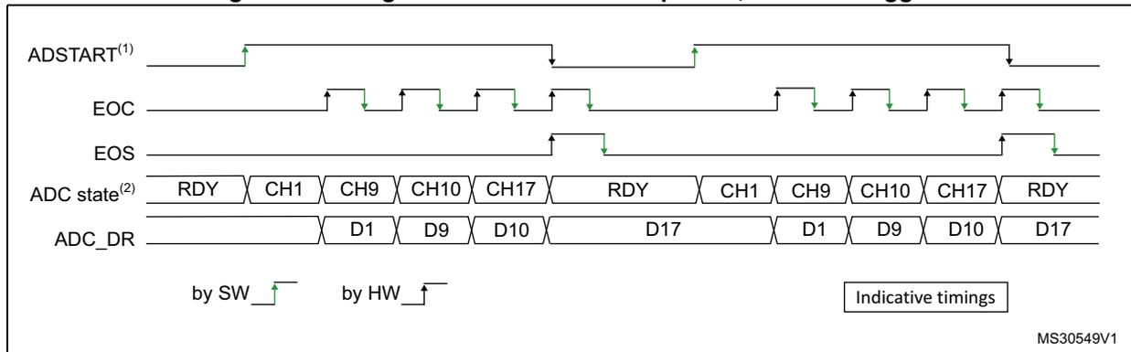
- 1. EXTEN[1:0] = 0x0, CONT = 0
- 2. Channels selected = 1,9, 10, 17; AUTDLY = 0.
Figure 234. Continuous conversion of a sequence, software trigger
by SW ↑ by HW ↑ Indicative timings
MS30550V1
- 1. EXTEN[1:0] = 0x0, CONT = 1
- 2. Channels selected = 1, 9, 10, 17; AUTDLY = 0.
Figure 235. Single conversions of a sequence, hardware trigger
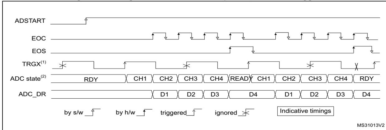
by s/w ↑ by h/w ↑ triggered ↑ ignored ✕ Indicative timings
MS31013V2
- 1. TRGx (over-frequency) is selected as trigger source, EXTEN[1:0] = 01, CONT = 0
- 2. Channels selected = 1, 2, 3, 4; AUTDLY = 0.
Figure 236. Continuous conversions of a sequence, hardware trigger
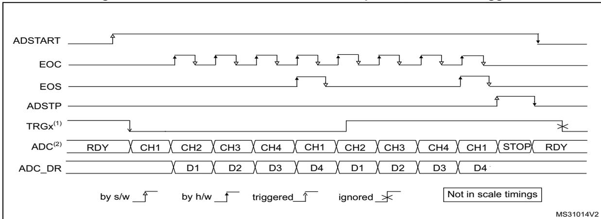
- 1. TRGx is selected as trigger source, EXTEN[1:0] = 10, CONT = 1
- 2. Channels selected = 1, 2, 3, 4; AUTDLY = 0.
33.4.26 Data management
Data register, data alignment and offset (ADC_DR, ADC_JDRy, OFFSETy, OFFSETy_CH, OVSS, LSHIFT, USAT, SSAT)
Data and alignment
At the end of each regular conversion channel (when the EOC event occurs), the result of the converted data is stored into the ADC_DR data register which is 32 bits wide.
At the end of each injected conversion channel (when the JEOC event occurs), the result of the converted data is stored into the corresponding ADC_JDRy data register which is 32 bits wide.
The OVSS[3:0] and LSHIFT[3:0] bitfields in the ADC_CFGR2 register selects the alignment of the data stored after conversion. By default, data are right-aligned. Refer to Figure 237 , Figure 238 , Figure 239 and Figure 240 for examples of data alignment.
Note: The data can be realigned in normal and in oversampling mode.
Offset
An offset y (y = 1,2,3,4) can be applied to a channel by programming a value different from 0 in the OFFSETy[23:0] bitfield of the ADC_OFRy register. The channel to which the offset is applied is programmed into the bits OFFSETy_CH[4:0] of ADC_OFRy register. The offset can be positive or negative depending on the value of the POSOFF bit. When POSOFF is cleared, the converted value is subtracted by the user-defined offset written in OFFSETy[23:0] bits. The result can be a negative value. The read data is consequently signed and the SEXT bit represents the extended sign value.
The offset value must be lower than the maximum conversion value (for example, in 14-bit mode, the maximum offset value is 0x3FFF).
The offset can be used to convert unsigned data to signed data (for example, in 14-bit mode, the offset value is equal to 0x2000).
The offset correction is also supported in oversampling mode. For the oversampling mode, offset is subtracted before OVSS right shift applied.
Table 313 describes how the comparison is performed for all the possible resolutions for analog watchdog 1, 2, 3.
Table 313. Offset computation versus data resolution
| Resolution (bits RES[1:0]) | Subtraction/addition between raw converted data and offset | Result | Comments | |
|---|---|---|---|---|
| Raw - converted left -aligned data | Offset | |||
| 00: 14-bit | DATA[13:0] | OFFSET[13:0] | Signed or unsigned 24-bit data, right aligned to [13:0] | - |
| 01: 12-bit | DATA[13:2],00 | OFFSET[13:2] | Signed or unsigned 24-bit data, right aligned to [11:0] | The user must configure OFFSET[11:0] to 0b0000 0000 0000. |
| 10: 10-bit | DATA[13:4],00 00 | OFFSET[13:4] | Signed or unsigned 24-bit data, right aligned to [9:0] | The user must configure OFFSET[3:0] to 0b0000. |
| 11: 8-bit | DATA[13:6],00 0000 | OFFSET[13:6] | Signed or unsigned 24-bit data, right aligned to [7:0] | The user must configure OFFSET[5:0] to 0b000000. |
Figure 237, Figure 238, Figure 239 and Figure 240 show alignments for signed and unsigned data together with corresponding OVSS and LSHIFT values.
Figure 237. Right alignment (offset disabled, unsigned value)
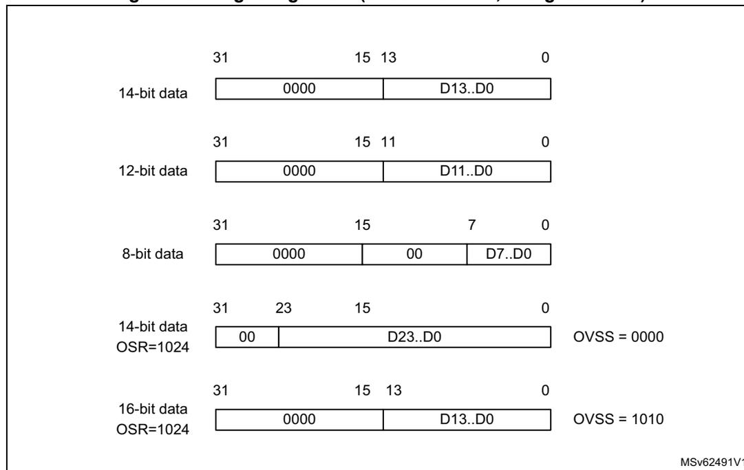
The diagram illustrates the right alignment of unsigned data for different resolutions and oversampling settings. It shows the mapping of data bits (Dn..D0) into a 32-bit register, with bit positions 31, 15, 13, 7, and 0 marked at the top.
- 14-bit data: Bits D13..D0 are aligned to the right (bits 13..0). The upper bits (31..14) are 0000.
- 12-bit data: Bits D11..D0 are aligned to the right (bits 11..0). The upper bits (31..12) are 0000.
- 8-bit data: Bits D7..D0 are aligned to the right (bits 7..0). The upper bits (31..8) are 0000.
- 14-bit data OSR=1024: Bits D23..D0 are aligned to the right (bits 23..0). The upper bits (31..24) are 00. OVSS = 0000.
- 16-bit data OSR=1024: Bits D13..D0 are aligned to the right (bits 13..0). The upper bits (31..14) are 0000. OVSS = 1010.
MSv62491V1
Figure 238. Right alignment (offset enabled, signed value)
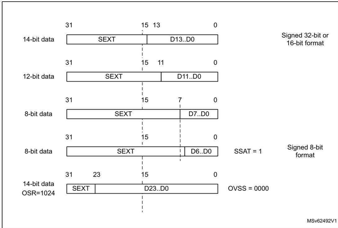
The diagram illustrates the right alignment of ADC data for different bit widths. Each row shows a 32-bit register structure with bit positions 31, 15, 13, 11, 7, and 0 marked. The data is right-aligned, meaning the least significant bit (D0) is always at position 0.
- 14-bit data: Bits D13..D0 are at positions 13..0. Bits 31..14 are filled with SEXT (sign extension). Labeled as "Signed 32-bit or 16-bit format".
- 12-bit data: Bits D11..D0 are at positions 11..0. Bits 31..12 are filled with SEXT.
- 8-bit data: Bits D7..D0 are at positions 7..0. Bits 31..8 are filled with SEXT.
- 8-bit data (SSAT = 1): Bits D6..D0 are at positions 6..0. Bits 31..7 are filled with SEXT. Labeled as "Signed 8-bit format".
- 14-bit data (OSR=1024): Bits D23..D0 are at positions 23..0. Bits 31..24 are filled with SEXT. Labeled as "OVSS = 0000".
MSv62492V1
Figure 239. Left alignment (offset disabled, unsigned value)
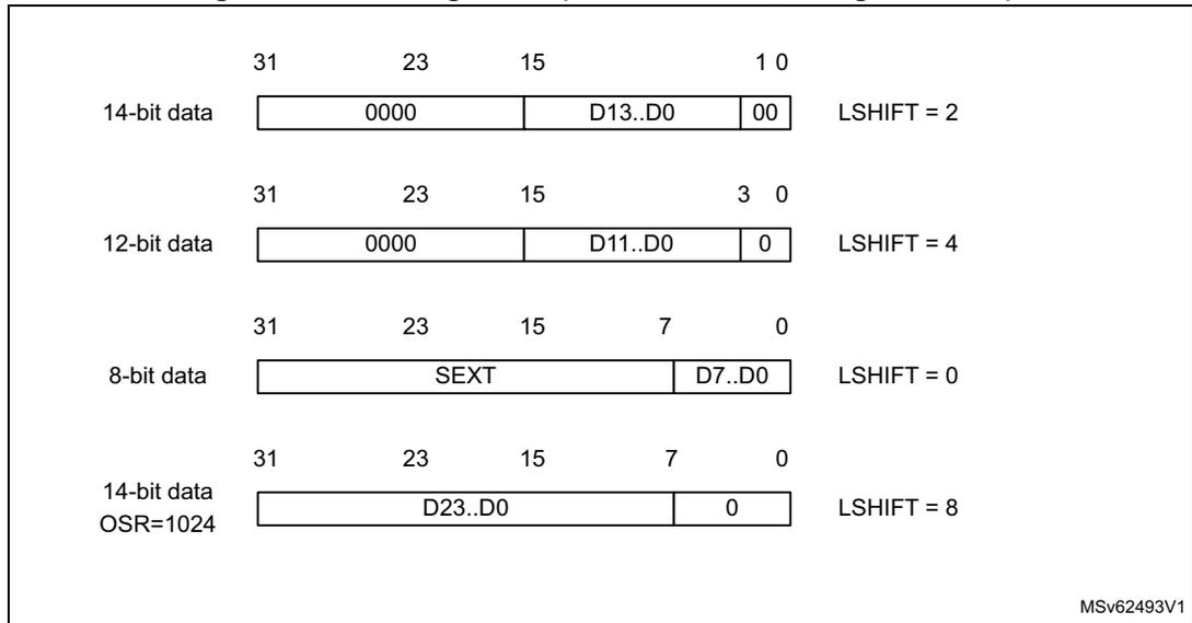
The diagram illustrates the left alignment of ADC data for different bit widths. Each row shows a 32-bit register structure with bit positions 31, 23, 15, 7, 1, and 0 marked. The data is left-aligned, meaning the most significant bit is at position 31.
- 14-bit data: Bits D13..D0 are at positions 23..10. Bits 31..24 are 0000. Bits 1..0 are 00. Labeled as "LSHIFT = 2".
- 12-bit data: Bits D11..D0 are at positions 23..12. Bits 31..24 are 0000. Bit 1 is 3, bit 0 is 0. Labeled as "LSHIFT = 4".
- 8-bit data: Bits D7..D0 are at positions 23..16. Bits 31..8 are filled with SEXT (sign extension). Labeled as "LSHIFT = 0".
- 14-bit data (OSR=1024): Bits D23..D0 are at positions 31..8. Bits 7..0 are 0. Labeled as "LSHIFT = 8".
MSv62493V1
Figure 240. Left alignment (offset enabled, signed value)
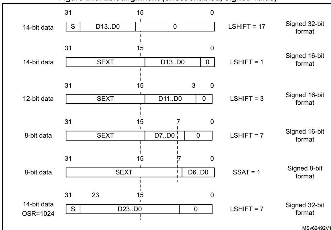
The diagram illustrates the internal 32-bit register format for different ADC resolutions with left alignment and signed values. Bit positions 31, 15, 0, 3, 7, and 23 are marked at the top. The formats are as follows:
- 14-bit data: Bit 31 is 'S', bits 13-0 are 'D13..D0', bits 15-1 are '0'. LSHIFT = 17. Signed 32-bit format.
- 14-bit data: Bits 31-16 are 'SEXT', bits 15-1 are 'D13..D0', bit 0 is '0'. LSHIFT = 1. Signed 16-bit format.
- 12-bit data: Bits 31-16 are 'SEXT', bits 15-3 are 'D11..D0', bits 2-0 are '0'. LSHIFT = 3. Signed 16-bit format.
- 8-bit data: Bits 31-16 are 'SEXT', bits 15-8 are 'D7..D0', bits 7-0 are '0'. LSHIFT = 7. Signed 16-bit format.
- 8-bit data: Bits 31-7 are 'SEXT', bits 6-0 are 'D6..D0'. SSAT = 1. Signed 8-bit format.
- 14-bit data OSR=1024: Bit 31 is 'S', bits 23-16 are 'D23..D0', bits 15-0 are '0'. LSHIFT = 7. Signed 32-bit format.
MSv62492V1
Management of signed and unsigned saturation format (SSAT, USAT)
The offset correction might result in the data width to be wider than the original data.
To limit the original width, the data saturation can be enabled through the SSAT and USAT bits of the ADC_OFRy register.
Unsigned 14-bit data can be extended to 15-bit signed data by using an offset value different from 0x2000.
The original data width can be preserved by setting the SSAT bit to limit the data width to 14 bits.
Unsigned data can be saturated to the original data width by setting the USAT bit.
Table 314 shows the sign-extended data format corresponding to different resolutions.
Table 314. 14-bit data formats
| SSAT | USAT | Format | Data range (offset = 0x2000) |
|---|---|---|---|
| 0 | 0 | Sign-extended 15-bit significant data: SEXT[31:14] DATA[13:0] | 0x0000 1FFF - 0xFFFF E000 |
| 1 | 0 | Sign-extended 14-bit significant data: SEXT[31:13] DATA[12:0] | 0x1FFF - 0xE000 |
Table 314. 14-bit data formats (continued)
| SSAT | USAT | Format | Data range (offset = 0x2000) |
|---|---|---|---|
| 0 | 1 | Unsigned saturation14-bit significant data: DATA[13:0] | 0x3FFF - 0x0000 |
| 1 | 1 | Reserved | - |
Table 315 provides numerical examples for three different offset values.
Table 315. Numerical examples for 16-bit format
| Raw conversion result | Offset value | Result | Result | Result |
|---|---|---|---|---|
| SSAT = 0 USAT = 0 | SSAT = 0 USAT = 1 | SSAT = 1 USAT = 0 | ||
| 0x3FFF | 0x2000 | 0x0000 1FFF | 1FFF | 1FFF |
| 0x2000 | 0x0000 0000 | 0000 | 0000 | |
| 0x0000 | 0xFFFF E000 | E000 | E000 | |
| 0x3FFF | 0x2020 | 0x0000 1FDF | 1FDF | 1FDF |
| 0x2000 | 0xFFFF FFE0 | 0000 | FFE0 | |
| 0x0000 | 0xFFFF DFE0 | 0000 | DFE0 | |
| 0x3FFF | 0x1FE0 | 0x0000 201F | 201F | 1FFF |
| 0x2000 | 0x0000 0020 | 0020 | 0020 | |
| 0x0000 | 0xFFFF E020 | 0000 | E020 | |
| 0x3FFF | 0x20 | 0x0000 3FDF | 3FDF | 3FDF |
| 0x2000 | 0x0000 1FE0 | 1FE0 | 1FE0 | |
| 0x0000 | 0xFFFF FFE0 | 0000 | FFE0 |
Caution: SSAT must not be used in conjunction with USAT. No hardware check is performed to ensure that this recommendation is respected.
Gain compensation
When the GCOMP bit is set in the ADC_CFGR2 register, the gain compensation is activated on all converted data. After each conversion, data is calculated using the following formula.
As GCOMPCOEFF can be programmed from 0 to 16383, the actual gain compensation factor can range from 0 to 3.999756.
Before storing the resulting data in the RDATA or JDATAx registers, the LSB+1 value is evaluated to round up the data and minimize the error.
The gain compensation is also effective for the oversampling. When the gain compensation is used for the oversampling mode, the gain calculation is performed after the accumulation and right-shift operations to minimize the power consumption (the gain calculation is done
only once instead of at each conversion). The internal multiplier width is 32 bits and the input data width for the gain compensation must be less than 18 bits. When using oversampling with injected and regular conversion mode the bit ADC_CFGR2.ROVSM bit must be set to resume the pending conversion with the correct value.
ADC overrun (OVRMOD)
The overrun flag (OVR) notifies of that a buffer overrun event occurred when the regular converted data has not been read (by the CPU or the DMA) before ADC_DR FIFO (eight stages) is overflowed.
The OVR flag is set when a new conversion completes while the ADC_CR register FIFO was full. An interrupt is generated if the OVRIE bit is set.
When an overrun event occurs, the ADC is still operating and can continue converting unless the software decides to stop and reset the sequence by setting the ADSTP bit.
OVR flag is cleared by software by writing 1 to it.
Data can be configured to be preserved or overwritten when an overrun event occurs by programming the OVRMOD control bit of the ADC_CFGR1 register:
- • OVRMOD = 0
The overrun event preserves the data register from being overwritten: the old data is maintained up to ADC_DR FIFO depth (eight data) and the new conversion is discarded and lost. If OVR remains at 1, further conversions occur but the result data are also discarded. - • OVRMOD = 1
The data register is overwritten with the last conversion result and the previous unread data is lost. In this mode, ADC_DR FIFO is disabled. If OVR remains at 1, further conversions operate normally and the ADC_DR register always contains the latest converted data.
Figure 241. Example of overrun (OVRMOD = 0)
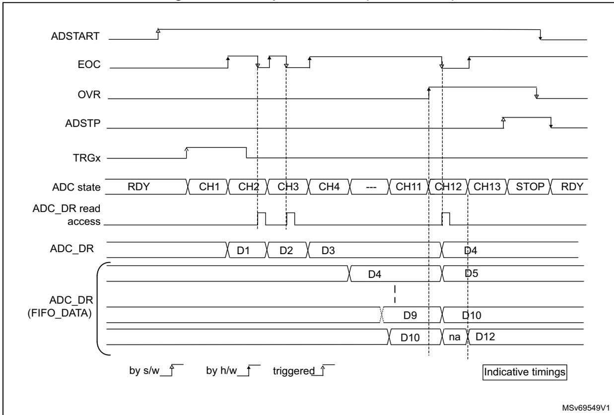
This timing diagram illustrates an overrun condition when OVRMOD = 0. The signals shown are:
- ADSTART : A software trigger that starts the ADC sequence.
- EOC : End of Conversion signal, which pulses when each channel's conversion is complete.
- OVR : Overrun flag, which goes high when a new conversion result is ready before the previous one has been read from the FIFO.
- ADSTP : A software stop signal for the ADC sequence.
- TRGx : An external trigger signal.
- ADC state : Shows the sequence of states: RDY, CH1, CH2, CH3, CH4, ..., CH11, CH12, CH13, STOP, RDY.
- ADC_DR read access : Shows software read accesses to the ADC_DR register.
- ADC_DR : The data register, showing values D1, D2, D3, D4, D5, D9, D10, D10, na, D12. The 'na' indicates a lost or invalid data point due to overrun.
- ADC_DR (FIFO_DATA) : The FIFO data register, showing the same sequence of values as ADC_DR.
Legend:
by s/w (software)
by h/w (hardware)
triggered
Indicative timings
MSv69549V1
Figure 242. Example of overrun (OVRMOD = 1)
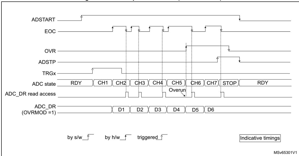
This timing diagram illustrates an overrun condition when OVRMOD = 1. The signals shown are:
- ADSTART : A software trigger that starts the ADC sequence.
- EOC : End of Conversion signal, which pulses when each channel's conversion is complete.
- OVR : Overrun flag, which goes high when a new conversion result is ready before the previous one has been read from the dedicated register.
- ADSTP : A software stop signal for the ADC sequence.
- TRGx : An external trigger signal.
- ADC state : Shows the sequence of states: RDY, CH1, CH2, CH3, CH4, CH5, CH6, CH7, STOP, RDY. An 'Overrun' label is present under CH5.
- ADC_DR read access : Shows software read accesses to the ADC_DR register.
- ADC_DR (OVRMOD = 1) : The data register, showing values D1, D2, D3, D4, D5, D6. No data is lost in this mode.
Legend:
by s/w (software)
by h/w (hardware)
triggered
Indicative timings
MSv65301V1
Note: There is no overrun detection on the injected channels since there is a dedicated data register for each of the four injected channels.
Managing a sequence of conversions without using the DMA
If the conversions are slow enough, the conversion sequence can be handled by the software. In this case, the software must use the EOC flag and its associated interrupt to handle each data. Each time a conversion is complete, EOC is set and the ADC_DR register can be read. OVRMOD must be configured to 0 to manage overrun events as an error.
Managing conversions without using the DMA and without overrun
It may be useful to let the ADC convert one or more channels without reading the data each time (for example if the device features an analog watchdog). In this case, the OVRMOD bit must be configured to 1 and the OVR flag must be ignored by the software. An overrun event does not prevent the ADC from continuing to convert and the ADC_DR register always contains the latest conversion.
Managing conversions using the DMA
Since converted channel values are stored in a unique data register, it is useful to use DMA to convert more than one channel. This avoids the loss of the data already stored in the ADC_DR register.
When the DMA mode is enabled (DMNGT[1:0] = 01 or 11 in the ADC_CFGR register in single ADC mode or DAMDF different from 00 in dual ADC mode), a DMA request is generated after each conversion of a channel. This allows the transfer of the converted data from the ADC_DR register to the destination location selected by the software.
Despite this, if an overrun occurs (OVR = 1) because the DMA cannot serve the DMA transfer request in time, the ADC stops generating DMA requests and the data corresponding to the new conversion is not transferred by the DMA. This means that all the data transferred to the RAM can be considered as valid.
Depending on the configuration of the OVRMOD bit, the data is either preserved or overwritten.
The DMA transfer requests are blocked until the software clears the OVR bit.
Two different DMA modes are proposed depending on the application. They can be configured through the DMNGT[1:0] bitfield of the ADC_CFGR1 register and the DAMDF bit of the ADC12_CCR register, in single ADC mode and in dual ADC mode, respectively:
- • DMA one shot mode (DMNGT[1:0] = 01).
This mode is suitable when the DMA is programmed to transfer a fixed number of data. - • DMA circular mode (DMNGT[1:0] = 11)
This mode is suitable when programming the DMA in circular mode.
DMA one shot mode (DMNGT[1:0] = 01)
In this mode, the ADC generates a DMA transfer request each time a new conversion data is available and stops generating DMA requests once the DMA has reached the last DMA transfer (when a transfer complete interrupt occurs - refer to DMA section) even if a conversion has been started again.
When the DMA transfer is complete (all the transfers configured in the DMA controller have been done):
- • The content of the ADC data register is frozen.
- • Any ongoing conversion is aborted with partial result discarded.
- • No new DMA request is issued to the DMA controller. This avoids generating an overrun error if there are still conversions, which are started.
- • Scan sequence is stopped and reset.
- • The DMA is stopped.
DMA circular mode (DMNGT[1:0] = 11)
In this mode, the ADC generates a DMA transfer request each time a new conversion data is available in the data register, even if the DMA has reached the last DMA transfer. This allows configuring the DMA in circular mode to handle a continuous analog input data stream.
DMA with FIFO
The output data register features an eight-stage FIFO. Two different DMA requests are generated in parallel. When a data is available, an “SREQ single request” is generated. When four data are available, a “BREQ burst request” is generated. DMA can be programmed either single transfer mode or incremental burst mode (four beats), according to this mode, correct request line is selected by the DMA. Refer to the DMA chapter for further information.
33.4.27 Managing conversions using the MDF
The ADC conversion results can be transferred directly to the MDF.
In this case, the DMNGT[1:0] bits must be set to 10.
The ADC transfers the 16 least significant bits of the regular data register to the MDF through
adcx_dat[15:0]
bus, which in turn resets the EOC flag once the transfer is effective.
The data format must be in 16-bit signed format:
ADC_DR[31:16]
= don't care
ADC_DR[15]
= sign
ADC_DR[14:0]
= data
Any value above 16-bit signed format is truncated.
33.4.28 Dynamic low-power features
Auto-delayed conversion mode (AUTDLY)
The ADC implements an auto-delayed conversion mode controlled by the AUTDLY configuration bit. Auto-delayed conversions are useful to simplify the software as well as to optimize performance of an application clocked at low frequency where there would be risk of encountering an ADC overrun.
When
AUTDLY = 1
, a new conversion can start only if all the previous data of the same group has been treated:
- • For a regular conversion: once the
ADC_DRregister has been read or if the EOC bit has been cleared (see Figure 243 ). - • For an injected conversion: when the JEOS bit has been cleared (see Figure 244 ).
The auto-delayed conversion mode enables to automatically adapt the speed of the ADC to the speed of the system which reads the data.
The delay is inserted after each regular conversion (whatever DISCEN = 0 or 1) and after each sequence of injected conversions (whatever JDISCEN = 0 or 1).
Note: There is no delay inserted between each conversion of the injected sequence, except after the last one.
During a conversion, a hardware trigger event (for the same group of conversions) occurring during this delay is ignored.
Note: This is not true for software triggers where it remains possible during this delay to set the bits ADSTART or JADSTART to restart a conversion: it is up to the software to read the data before launching a new conversion.
No delay is inserted between conversions of different groups (a regular conversion followed by an injected conversion or conversely):
- • If an injected trigger occurs during the automatic delay of a regular conversion, the injected conversion starts immediately (see Figure 244 ).
- • Once the injected sequence is complete, the ADC waits for the delay (if not ended) of the previous regular conversion before launching a new regular conversion (see Figure 246 ).
The behavior is slightly different in auto-injected mode (JAUTO = 1) where a new regular conversion can start only when the automatic delay of the previous injected sequence of conversion has ended (when JEOS has been cleared). This is to ensure that the software can read all the data of a given sequence before starting a new sequence (see Figure 247 ).
To stop a conversion in continuous auto-injection mode combined with auto-delay mode (JAUTO = 1, CONT = 1 and AUTDLY = 1), follow the following procedure:
- 1. Wait until JEOS = 1 (no more conversions are restarted).
- 2. Clear JEOS.
- 3. Set ADSTP = 1.
- 4. Read the regular data.
If this procedure is not respected, a new regular sequence can restart if JEOS is cleared after ADSTP has been set.
In AUTDLY mode, a hardware regular trigger event is ignored if it occurs during an already ongoing regular sequence or during the delay that follows the last regular conversion of the sequence. It is however considered pending if it occurs after this delay, even if it occurs during an injected sequence or during the delay that follows it. The conversion then starts at the end of the delay of the injected sequence.
In AUTDLY mode, a hardware injected trigger event is ignored if it occurs during an already ongoing injected sequence or during the delay that follows the last injected conversion of the sequence.
Figure 243. AUTDLY = 1, regular conversion in continuous mode, software trigger
- 1. AUTDLY = 1.
- 2. Regular configuration: EXTEN[1:0] = 0x0 (software trigger), CONT = 1, CHANNELS = 1,2,3.
- 3. Injected configuration DISABLED.
Figure 244. AUTDLY = 1, regular hardware conversions interrupted by injected conversions (DISCEN = 0; JDISCEN = 0)
- 1. AUTDLY = 1.
- 2. Regular configuration: EXTEN[1:0] = 0x1 (hardware trigger), CONT = 0, DISCEN = 0, CHANNELS = 1, 2, 3.
- 3. Injected configuration: JEXTEN[1:0] = 0x1 (hardware Trigger), JDISCEN = 0, CHANNELS = 5,6.
Figure 245. AUTODLY = 1, regular hardware conversions interrupted by injected conversions (DISCEN = 1, JDISCEN = 1)
The diagram illustrates the timing of regular and injected conversions in the ADC12 when AUTODLY = 1, DISCEN = 1, and JDISCEN = 1. The sequence starts with a regular trigger (by SW) and proceeds through a series of regular conversions (CH1, CH2, CH3) and injected conversions (CH5, CH6). Delays (DLY) are applied between conversions. The diagram shows that injected conversions can interrupt the regular sequence, and that regular conversions are ignored if they occur during an injected sequence. The ADC state transitions between RDY (Ready) and CHx (Conversion in progress). The EOC (End of Conversion) signal is generated at the end of each sequence. The ADC_DR (Data Register) is updated with the conversion results (D1, D2, D3, D5, D6). The injected trigger (by HW) initiates the injected sequence. The JEOS (End of Injected Sequence) signal is generated at the end of the injected sequence. The ADC_JDR1 and ADC_JDR2 registers are updated with the injected conversion results (D5, D6). The legend indicates that solid lines represent software (SW) triggers and dashed lines represent hardware (HW) triggers. The text 'Indicative timings' is present in the bottom right corner of the diagram area.
MS31022V1
- 1. AUTODLY = 1.
- 2. Regular configuration: EXTEN[1:0] = 0x1 ( hardware trigger), CONT = 0, DISCEN = 1, DISCNUM = 1, CHANNELS = 1, 2, 3.
- 3. Injected configuration: JEXTEN[1:0] = 0x1 (hardware Trigger), JDISCEN = 1, CHANNELS = 5,6.
Figure 246. AUTODLY = 1, regular continuous conversions interrupted by injected conversions
Timing diagram for Figure 246. The diagram shows the sequence of conversions and the associated delays. The ADC state starts at RDY and transitions through CH1 (regular), DLY (CH1), CH2 (regular), DLY (CH2), CH5 (injected), CH6 (injected), DLY (ignored), CH3 (regular), DLY (CH3), and CH1 (regular). The EOC signal is shown for each regular conversion. The ADC_DR read access is shown for each regular conversion. The injected trigger is shown for the injected conversions. The JEOS signal is shown for the injected conversions. The ADC_JDR1 and ADC_JDR2 registers are shown for the injected conversions. The data values D1, D2, D3, D5, and D6 are indicated for the respective channels. The diagram is labeled with 'by s/w' and 'by h/w' for the start of conversions. A legend indicates 'Indicative timings'.
MS31023V3
- 1. AUTODLY = 1.
- 2. Regular configuration: EXTEN[1:0] = 0x0 (software trigger), CONT = 1, DISCEN = 0, CHANNELS = 1, 2, 3.
- 3. Injected configuration: JEXTEN[1:0] = 0x1 (hardware trigger), JDISCEN = 0, CHANNELS = 5,6.
Figure 247. AUTODLY = 1 in auto- injected mode (JAUTO = 1)
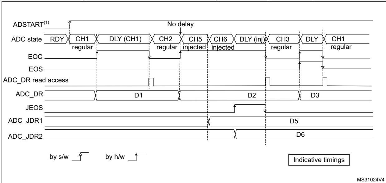
Timing diagram for Figure 247. The diagram shows the sequence of conversions and the associated delays. The ADC state starts at RDY and transitions through CH1 (regular), DLY (CH1), CH2 (regular), CH5 (injected), CH6 (injected), DLY (inj), CH3 (regular), DLY, and CH1 (regular). The 'No delay' label is shown between CH2 and CH5. The EOC signal is shown for each regular conversion. The ADC_DR read access is shown for each regular conversion. The JEOS signal is shown for the injected conversions. The ADC_JDR1 and ADC_JDR2 registers are shown for the injected conversions. The data values D1, D2, D3, D5, and D6 are indicated for the respective channels. The diagram is labeled with 'by s/w' and 'by h/w' for the start of conversions. A legend indicates 'Indicative timings'.
MS31024V4
- 1. AUTODLY = 1.
- 2. Regular configuration: EXTEN[1:0] = 0x0 (software trigger), CONT = 1, DISCEN = 0, CHANNELS = 1, 2.
- 3. Injected configuration: JAUTO = 1, CHANNELS = 5,6.
33.4.29 Analog window watchdog (AWD1EN, JAWD1EN, AWD1SGL, AWD1CH, AWD2CH, AWD3CH, AWD_HTRy, AWD_LTRy, AWDy)
The three AWD analog watchdogs monitor whether some channels remain within a configured voltage range (window).
Figure 248. Analog watchdog guarded area

AWDx flag and interrupt
An interrupt can be enabled for each of the three analog watchdogs by setting AWDyIE in the ADC_IER register (y = 1, 2, 3).
AWDy (y = 1, 2, 3) flag is cleared by software by writing 1 to it.
The ADC conversion result is compared to the lower and higher thresholds before alignment.
Description of analog watchdog 1
The AWD analog watchdog 1 is enabled by setting the AWD1EN bit in the ADC_CFGR1 register. This watchdog monitors whether either one selected channel or all enabled channels remain within a configured voltage range (window).
Table 316 shows how the ADC_CFGR1 registers must be configured to enable the analog watchdog on one or more channels.
Table 316. Analog watchdog channel selection
| Channels guarded by the analog watchdog | AWD1SGL bit | AWD1EN bit | JAWD1EN bit |
|---|---|---|---|
| None | x | 0 | 0 |
| All injected channels | 0 | 0 | 1 |
| All regular channels | 0 | 1 | 0 |
| All regular and injected channels | 0 | 1 | 1 |
| Single (1) injected channel | 1 | 0 | 1 |
| Single (1) regular channel | 1 | 1 | 0 |
| Single (1) regular or injected channel | 1 | 1 | 1 |
1. Selected by the AWDyCH[4:0] bits. The channels must also be programmed to be converted in the appropriate regular or injected sequence.
The AWD1 analog watchdog status bit is set if the analog voltage converted by the ADC is below a lower threshold or above a higher threshold.
These thresholds are programmed in the HTR1[24:0] bits of the ADC_HTR1 register and LTR1[24:0] of the ADC_LTR1 register for the analog watchdog 1.
The threshold can be up to 25-bits (14-bit resolution with oversampling, OSR=256).
When converting data with a resolution of less than 14 bits (according to bits RES[1:0]), the LSBs of the programmed thresholds must be kept cleared, the internal comparison being performed on the full 14-bit converted data (left aligned to the half-word boundary).
Table 317 describes how the comparison is performed for all the possible resolutions for analog watchdog 1,2,3.
Table 317. Analog watchdog 1,2,3 comparison
| Resolution (bit RES[1:0]) | Analog watchdog comparison between: | Comments | |
|---|---|---|---|
| Raw converted data, left aligned (1) | Thresholds | ||
| 00: 14-bit | DATA[13:0] | LTR1[24:0] and HTR1[24:0] | - |
| 01: 12-bit | DATA[13:2],00 | LTR1[24:0] and HTR1[24:0] | User must configure LTR1[1:0] and HTR1[1:0] to 00 |
| 10: 10-bit | DATA[13:4],0000 | LTR1[24:0] and HTR1[24:0] | User must configure LTR1[3:0] and HTR1[3:0] to 0000 |
| 11: 8-bit | DATA[13:6],000000 | LTR1[24:0] and HTR1[24:0] | User must configure LTR1[5:0] and HTR1[5:0] to 000000 |
- 1. The watchdog comparison is performed when the oversampling, the gain compensation and the offset compensation are complete (the data that are compared can be either signed or unsigned).
Analog watchdog filter for watchdog 1
When the ADC is configured with only one input channel (selecting several channels in scan mode not allowed), a valid ADC conversion data range can be configured through the ADC_LTR1 and ADC_HTR1 register:
- • When converted data belong to the range defined in ADC_LTR1 and ADC_HTR1, the AWD1 flag remains cleared.
- • If data are out-of-range a number of times higher than the value specified in the AWDFILT bit of ADC_HTR1, the AWD1 flag is set and the corresponding interrupt is issued.
Description of analog watchdog 2 and 3
The second and third analog watchdogs are more flexible and can guard several selected channels by programming the corresponding bits in AWDCHy[19:0] (y=2,3).
The corresponding watchdog is enabled when any bit of AWDCHy[19:0] (y=2,3) is set.
The threshold can be up to 25 bits (14-bit resolution with oversampling, OSR = 1024, and offset conversion in signed format) and are programmed with the ADC_HTR2, ADC_LTR2, ADC_HTR3, and ADC_LTR3 registers.
When converting data with a resolution of less than 14 bits (according to bits RES[1:0]), the LSBs of the programmed thresholds must be kept cleared, the internal comparison being performed on the full 14-bit converted data (left aligned).
ADC_AWDy_OUT signal output generation
Each analog watchdog is associated to an internal hardware signal ADC_AWDy_OUT (y being the watchdog number) which is directly connected to the ETR input (external trigger)
of some on-chip timers. Refer to the on-chip timers section to understand how to select the ADC_AWDy_OUT signal as ETR.
ADC_AWDy_OUT is activated when the associated analog watchdog is enabled:
- • ADC_AWDy_OUT is set when a guarded conversion is outside the programmed thresholds.
- • ADC_AWDy_OUT is reset after the end of the next guarded conversion which is inside the programmed thresholds (it remains at 1 if the next guarded conversions are still outside the programmed thresholds).
- • ADC_AWDy_OUT is also reset when disabling the ADC (when setting ADDIS = 1). Note that stopping regular or injected conversions (setting ADSTP = 1 or JADSTP = 1) has no influence on the generation of ADCy_AWDx_OUT.
Note: AWDx flag is set by hardware and reset by software: AWDy flag has no influence on the generation of ADC_AWDy_OUT (ex: ADCy_AWDy_OUT can toggle while AWDx flag remains at 1 if the software did not clear the flag).
Figure 249. ADCy_AWDx_OUT signal generation (on all regular channels)
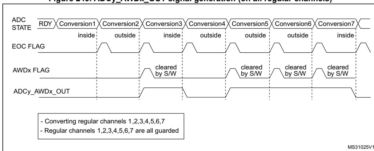
The diagram shows the following signals over time for seven conversions:
- ADC STATE: Starts at RDY, then shows Conversion1 (inside), Conversion2 (outside), Conversion3 (inside), Conversion4 (outside), Conversion5 (outside), Conversion6 (outside), Conversion7 (inside).
- EOC FLAG: Pulses high at the end of each conversion.
- AWDx FLAG: Goes high when a conversion is 'outside' (Conversions 2, 4, 5, 6). It is manually cleared by software (S/W) after each 'outside' conversion, returning to low before the next conversion starts.
- ADCy_AWDx_OUT: Goes high when the AWDx FLAG is high (during 'outside' conversions) and returns to low when the AWDx FLAG is low.
Legend:
- - Converting regular channels 1,2,3,4,5,6,7
- - Regular channels 1,2,3,4,5,6,7 are all guarded
MS31025V1
Figure 250. ADC_AWDx_OUT signal generation (AWDx flag not cleared by software)
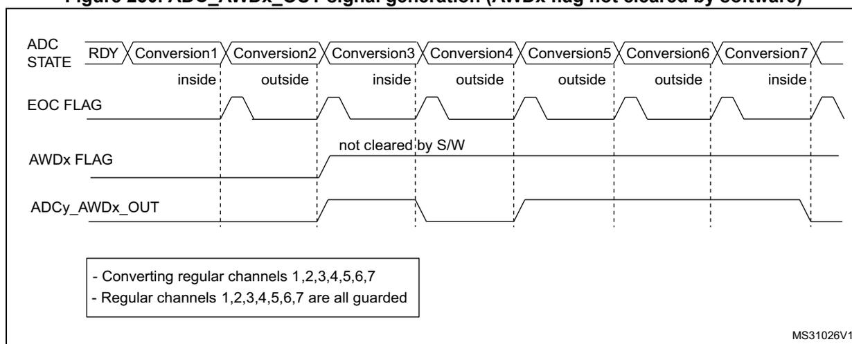
The diagram shows the following signals over time for seven conversions:
- ADC STATE: Starts at RDY, then shows Conversion1 (inside), Conversion2 (outside), Conversion3 (inside), Conversion4 (outside), Conversion5 (outside), Conversion6 (outside), Conversion7 (inside).
- EOC FLAG: Pulses high at the end of each conversion.
- AWDx FLAG: Goes high when Conversion2 is 'outside'. It remains high ('not cleared by S/W') through Conversion3 (inside), and only returns to low after Conversion7 (inside) is complete.
- ADCy_AWDx_OUT: Goes high when Conversion2 is 'outside' and remains high until after Conversion7 is complete.
Legend:
- - Converting regular channels 1,2,3,4,5,6,7
- - Regular channels 1,2,3,4,5,6,7 are all guarded
MS31026V1
Figure 251. ADC_AWDx_OUT signal generation (on a single regular channel)
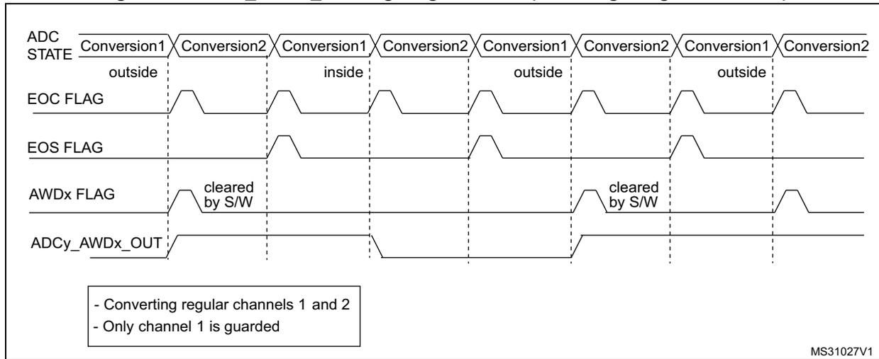
Legend:
- - Converting regular channels 1 and 2
- - Only channel 1 is guarded
MS31027V1
Figure 252. ADC_AWDx_OUT signal generation (on all injected channels)
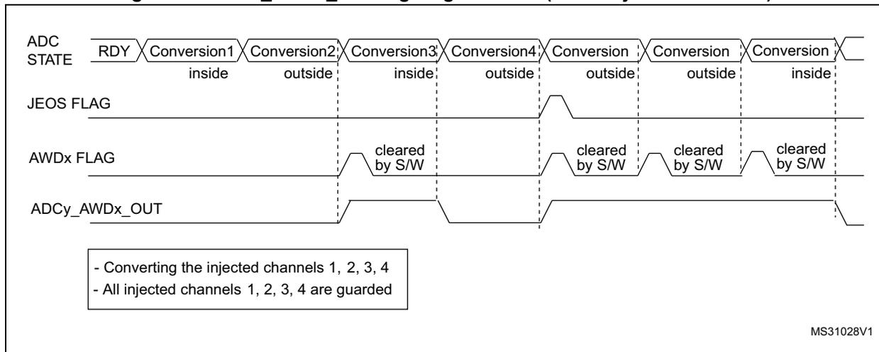
Legend:
- - Converting the injected channels 1, 2, 3, 4
- - All injected channels 1, 2, 3, 4 are guarded
MS31028V1
Analog watchdog threshold control
LTRx[24:0] and HTRx[24:0] can be changed when an analog-to-digital conversion is ongoing (that is between the start of conversion and the end of conversion of the ADC internal state). If LTRx[24:0] and HTRx[24:0] are updated during the ADC conversion of the ADC guarded channel, the watchdog function is masked for this conversion. This masking is removed at the next start of conversion, resulting in an analog watchdog thresholds to be applied from the next ADC conversion. The analog watchdog comparison is performed at each end of conversion. If the current ADC data is out of the new interval, no interrupt and AWDx_OUT signal are issued. The interrupt and the AWD generation only happen at the end of the conversion which started after the threshold update. If AWD_xOUT is already asserted, programming the new thresholds does not deassert the AWD_OUT signal.
Analog watchdog with gain and offset compensation
When gain and offset compensation are enabled, the analog watchdog compares the threshold after the compensated data.
33.4.30 Oversampler
The oversampling unit performs data preprocessing to offload the CPU. It is able to handle multiple conversions and average them into a single data with increased data width, up to 24-bit (14-bit values and OSR = 1024).
It provides a result with the following form, where N and M can be adjusted:
It enables the following functions to be performed by hardware: averaging, data rate reduction, SNR improvement, basic filtering.
The oversampling ratio N is defined using the OSR[9:0] bits in the ADC_CFGR2 register, and can range from 2x to 1024x. The division coefficient M consists of a right bit shift up to 10 bits, and is defined using the OVSS[3:0] bits in the ADC_CFGR2 register.
The summation unit can yield a result up to 24 bits (1024 x 14-bit results), which can be left or right shifted. When right shifting is selected, it is rounded to the nearest value using the least significant bits left apart by the shifting, before being transferred into the ADC_DR data register.
Figure 253 gives a numerical example of the processing, from a raw 24-bit accumulated data to the final 14-bit result.
Figure 253. 14-bit result oversampling with 10-bits right shift and rounding
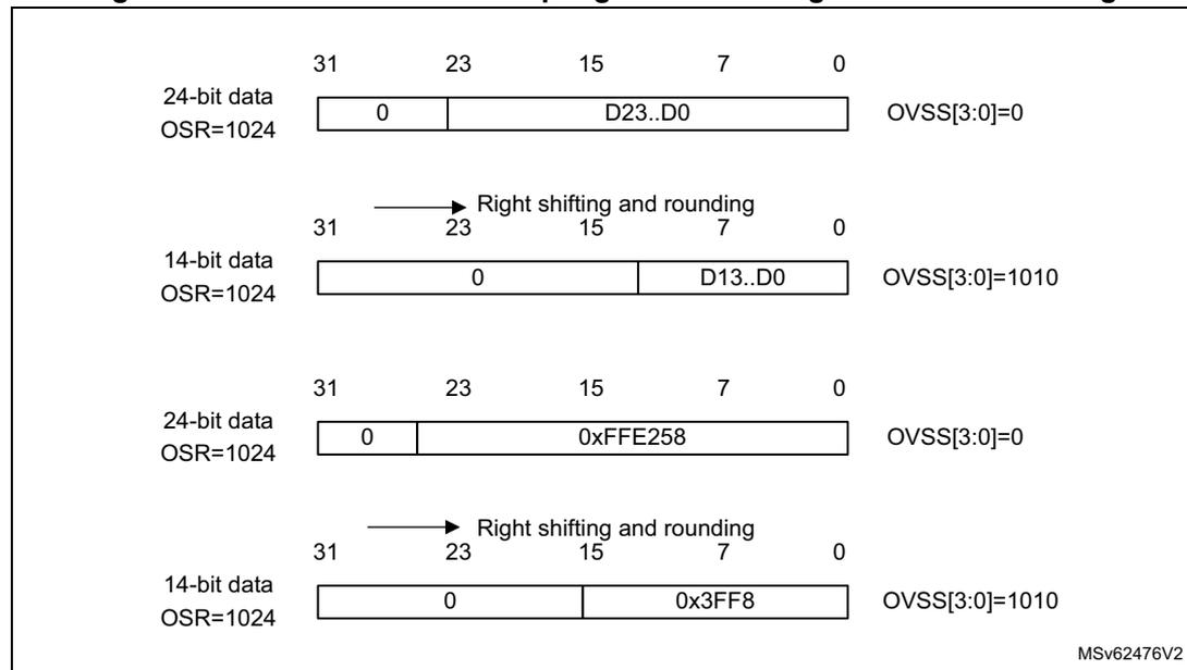
The diagram illustrates the processing of 24-bit accumulated data into a 14-bit result using right shifting and rounding. It shows two examples of this process.
Example 1:
- 24-bit data (OSR=1024): A 32-bit register with bits 31, 23, 15, 7, and 0. Bit 31 is 0, and bits 23-0 are labeled D23..D0. The OVSS[3:0] register is set to 0.
- Right shifting and rounding: An arrow indicates a right shift of 10 bits. The resulting 14-bit data is shown in a 32-bit register with bits 31, 23, 15, 7, and 0. Bit 31 is 0, and bits 13-0 are labeled D13..D0. The OVSS[3:0] register is set to 1010.
Example 2:
- 24-bit data (OSR=1024): A 32-bit register with bits 31, 23, 15, 7, and 0. Bit 31 is 0, and bits 23-0 contain the value 0xFFE258. The OVSS[3:0] register is set to 0.
- Right shifting and rounding: An arrow indicates a right shift of 10 bits. The resulting 14-bit data is shown in a 32-bit register with bits 31, 23, 15, 7, and 0. Bit 31 is 0, and bits 13-0 contain the value 0x3FF8. The OVSS[3:0] register is set to 1010.
MSv62476V2
The conversion timings in oversampling mode do not change: the sample time is maintained during the whole oversampling sequence. A new data is provided every N conversions with an equivalent delay equal to \( N \times T_{\text{CONV}} = N \times (t_{\text{SAMPL}} + t_{\text{SAR}}) \) . The flags are set as follows:
- • The end of the sampling phase (EOSMP) is set after each sampling phase.
- • The end of conversion (EOC) occurs once every N conversions, when the oversampled result is available.
- • The end of sequence (EOS) occurs once the sequence of oversampled data is completed (i.e. after N x sequence length conversions total).
Operating modes supported during oversampling
In oversampling mode, most of the ADC operating modes are maintained:
- • Single or continuous mode conversions
- • ADC conversions start either by software or with triggers
- • ADC stop during a conversion (abort)
- • Data read via CPU or DMA with overrun detection
- • Low-power modes (AUTDLY)
- • Programmable resolution: in this case, the reduced conversion values (configured through the RES[1:0] bits of the ADC_CFGR1 register) are accumulated, truncated, rounded, and shifted in the same way as 14-bit conversions.
Note: The alignment mode is not available when working with oversampled data. The ALIGN bit in ADC_CFGR is ignored and the data are always provided right-aligned.
Analog watchdog
The analog watchdog functionality is maintained, with the following differences:
- • The RES[1:0] bits are ignored. The comparison is always done using the full 25-bit values, HTRx[24:0] and LTRx[24:0].
- • The comparison is performed on the oversampled accumulated value before shifting.
Note: Care must be taken when using high shifting values, since this reduces the comparison range. For instance, if the oversampled result is shifted by 4 bits, thus yielding an 8-bit right-aligned data, the effective analog watchdog comparison can only be performed on 8 bits. The comparison is done between ADC_DR[11:4] and HT[7:0]/LT[7:0]. HT[11:8]/LT[11:8] must be kept reset.
Triggered mode
The averager can also be used for basic filtering purpose. Although not a very powerful filter (slow roll-off and limited stop band attenuation), it can be used as a notch filter to reject constant parasitic frequencies (typically coming from the mains or from a switched mode power supply). For this purpose, a specific discontinuous mode can be enabled with the TROVS bit of the DC_CFGR2, to be able to have an oversampling frequency defined by a user and independent from the conversion time itself.
The Figure 254 below shows how conversions are started in response to triggers during discontinuous mode.
If the TROVS bit is set, the content of the DISCEN bit is ignored and considered as 1.
Figure 254. Triggered regular oversampling mode (TROVS bit = 1)
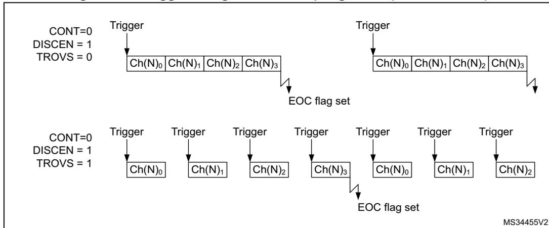
The diagram illustrates two examples of triggered regular oversampling mode (TROVS bit = 1) for an ADC12. Both examples show a sequence of channel conversions triggered by an external signal.
Top Example: Configuration: CONT=0, DISCEN = 1, TROVS = 0. A trigger initiates a sequence of four channel conversions: Ch(N) 0 , Ch(N) 1 , Ch(N) 2 , and Ch(N) 3 . The EOC flag is set after the last conversion (Ch(N) 3 ).
Bottom Example: Configuration: CONT=0, DISCEN = 1, TROVS = 1. A trigger initiates a sequence of seven channel conversions: Ch(N) 0 , Ch(N) 1 , Ch(N) 2 , Ch(N) 3 , Ch(N) 0 , Ch(N) 1 , and Ch(N) 2 . The EOC flag is set after the last conversion (Ch(N) 2 ).
The diagram is labeled MS34455V2.
Injected and regular sequencer management when oversampling
In oversampling mode, injected and regular sequencers can have different behaviors. The oversampling can be enabled for both sequencers with some limitations if they have to be used simultaneously (this is related to a unique accumulation unit).
Oversampling regular channels only
The regular oversampling mode bit, ROVSM, defines how the regular oversampling sequence is resumed if it is interrupted by injected conversion:
- • In continued mode, the accumulation restarts from the last valid data (prior to the conversion abort request due to the injected trigger). This ensures that oversampling is complete whatever the injection frequency (providing at least one regular conversion can be completed between triggers);
- • In resumed mode, the accumulation restarts from 0 (previous conversions results are ignored). This mode guarantees that all data used for oversampling were converted back-to-back within a single time-slot. Care must be taken to have an injection trigger period above the oversampling period length. If this condition is not respected, the oversampling cannot be completed and the regular sequencer is blocked.
Figure 255 gives examples for an oversampling ratio of 4x.
Figure 255. Regular oversampling modes (4x ratio)
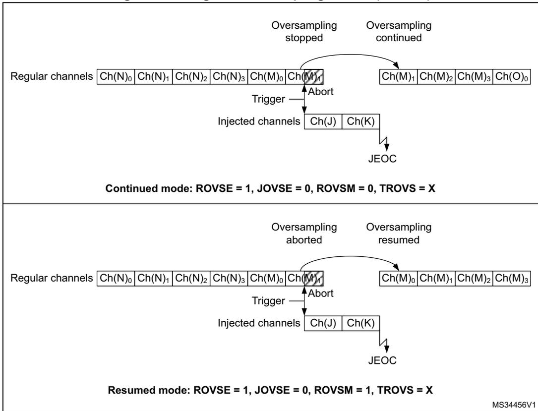
Continued mode: ROVSE = 1, JOVSE = 0, ROVSM = 0, TROVS = X
Resumed mode: ROVSE = 1, JOVSE = 0, ROVSM = 1, TROVS = X
MS34456V1
Oversampling injected channels only
The injected oversampling mode bit, JOVSE, enables oversampling solely for conversions in the injected sequencer.
Oversampling regular and injected channels
Both ROVSE and JOVSE bits can be set simultaneously. In this case, the regular oversampling mode is forced to resumed mode (ROVSM bit ignored), as shown in Figure 256.
Figure 256. Regular and injected oversampling modes used simultaneously
ROVSE = 1, JOVSE = 1, ROVSM = 1, TROVS = 0
MS34457V2
Triggered regular oversampling with injected conversions
Injected conversions can be performed in triggered regular mode. In this case, the injected mode oversampling mode must be disabled, and the ROVSM bit is ignored (resumed mode forced). The JOVSE bit must be reset. The behavior is shown in Figure 257 .
Figure 257. Triggered regular oversampling with injection
The diagram shows a sequence of ADC conversions. It starts with regular channel triggers for Ch(N) 0 and Ch(N) 1 . A third trigger occurs for Ch(N) 2 , but an injected trigger occurs simultaneously or shortly after, causing an 'Abort' of the regular conversion. Injected channels Ch(J) and Ch(K) are then converted. After the injected sequence, oversampling is resumed, starting again with Ch(N) 0 and Ch(N) 1 . The configuration settings shown are: ROVSE = 1, JOVSE = 0, ROVSM = 1, TROVS = 1.
Auto-injected mode
It is possible to oversample auto-injected sequences and have all conversions results stored in registers. This enables to save a DMA resource. This mode is available only when both regular and injected oversampling active: JAUTO = 1, ROVSE = 1 and JOVSE = 1. Other combinations are not supported. The ROVSM bit is ignored in auto-injected mode.
Figure 258 shows how the conversions are sequenced.
Figure 258. Oversampling in auto-injected mode
The diagram illustrates a continuous sequence of conversions. It begins with a block of regular channels: N 0 , N 1 , N 2 , N 3 . This is immediately followed by a long sequence of injected channels: I 0 , I 1 , I 2 , I 3 , J 0 , J 1 , J 2 , J 3 , K 0 , K 1 , K 2 , K 3 , L 0 , L 1 , L 2 , L 3 . After the injected sequence, the regular sequence N 0 , N 1 , N 2 , N 3 repeats. The configuration settings are: JAUTO = 1, ROVSE = 1, JOVSE = 1, ROVSM = X, TROVS = 0.
It is possible to have also the triggered mode enabled, using the TROVS bit. In this case, the ADC must be configured as follows: JAUTO = 1, DISCEN = 0, JDISCEN = 0, ROVSE = 1, JOVSE = 1 and TROVSE = 1.
Dual ADC modes support when oversampling
It is possible to have oversampling enabled when working in dual ADC configuration, for the injected simultaneous mode and regular simultaneous mode. In this case, the two ADCs must be programmed with the very same settings (including oversampling).
All other dual ADC modes are not supported when either regular or injected oversampling is enabled (ROVSE = 1 or JOVSE = 1).
Summary of combined modes
Table 318 summarizes all mode combinations, including non-supported modes.
Table 318. Summary of oversampler operating modes
| Regular oversampling: ROVSE bit | Injected oversampling: JOVSE bit | Oversampler mode: ROVSM bit 0 = continued 1 = resumed | Triggered regular mode: TROVS bit | Comment |
|---|---|---|---|---|
| 1 | 0 | 0 (continued) | 0 | Regular continued mode |
| 1 | 0 | 0 (continued) | 1 | Not supported |
| 1 | 0 | 1 (resumed) | 0 | Regular resumed mode |
| 1 | 0 | 1 (resumed) | 1 | Triggered regular resumed mode |
| 1 | 1 | 0 (continued) | X | Not supported |
| 1 | 1 | 1 (resumed) | 0 | Injected and regular resumed mode |
| 1 | 1 | 1 (resumed) | 1 | Not supported |
| 0 | 1 | X | X | Injected oversampling |
33.4.31 Dual ADC modes
In devices with two ADCs or more, dual ADC modes can be used (see Figure 33.4.32 ):
- • ADC1 and ADC2 can be used together in dual mode (ADC1 is master)
In dual ADC mode the start of conversion is triggered alternately or simultaneously by the ADCx master to the ADC slave, depending on the mode selected by the DUAL[4:0] bits of the ADC12_CCR register.
Four possible modes are implemented:
- • Injected simultaneous mode
- • Regular simultaneous mode
- • Interleaved mode
- • Alternate trigger mode
It is also possible to use these modes combined in the following ways:
- • Injected simultaneous mode + regular simultaneous mode
- • Regular simultaneous mode + alternate trigger mode
- • Injected simultaneous mode + interleaved mode
In dual ADC mode (when bits DUAL[4:0] in the ADC12_CCR register are not equal to zero), the bits CONT, AUTDLY, DISCEN, DISCNUM[2:0], JDISCEN, JAUTO of the ADC_CFGR register are shared between the master and slave ADC: the bits in the slave ADC are always equal to the corresponding bits of the master ADC.
To start a conversion in dual mode, the user must program the bits EXTEN[1:0], EXTSEL, JEXTEN[1:0], JEXTSEL of the master ADC only, to configure a software or hardware
trigger, and a regular or injected trigger. (the bits EXTEN[1:0] and JEXTEN[1:0] of the slave ADC are don't care).
In regular simultaneous or interleaved modes: once the user sets bit ADSTART or bit ADSTP of the master ADC, the corresponding bit of the slave ADC is also automatically set. However, bit ADSTART or bit ADSTP of the slave ADC is not necessary cleared at the same time as the master ADC bit.
In injected simultaneous or alternate trigger modes: once the user sets bit JADSTART or bit JADSTP of the master ADC, the corresponding bit of the slave ADC is also automatically set. However, bit JADSTART or bit JADSTP of the slave ADC is not necessary cleared at the same time as the master ADC bit.
In dual ADC mode, the converted data of the master and slave ADC can be read in parallel, by reading the ADC common data register (ADC12_CDR). The status bits can be also read in parallel by reading the dual-mode status register (ADC12_CSR).
Figure 259. Dual ADC block diagram (1)
The diagram illustrates the internal architecture of a Dual ADC system. It consists of two main ADC blocks: a Slave ADC at the top and a Master ADC at the bottom. Both ADCs have their own Regular channels and Injected channels . The Slave ADC's regular channels output to a Regular data register (32-bits) , and its injected channels output to Injected data registers (4 x32-bits) . The Master ADC has similar regular and injected channels, which output to their own respective Regular data register (32-bits) and Injected data registers (4 x32-bits) . All four data registers are connected to a common Address/data bus . Input sources for the ADCs include Internal analog inputs and GPIO ports (labeled with ADCx_INP0, ADCx_INN0, ADCx_INP2, ADCx_INN2, ..., ADCx_INP19, ADCx_INN19). The Master ADC features two Start trigger mux. units: one for the (regular group) and another for the (injected group) . These muxes are connected to Internal triggers and a Dual mode control block. The Slave ADC also receives Internal triggers . A small text label MSv41029V2 is located in the bottom right corner of the diagram.
- 1. External triggers also exist on slave ADC but are not shown for the purposes of this diagram.
- 2. The ADC common data register (ADC12_CDR) contains both the master and slave ADC regular converted data.
Injected simultaneous mode
This mode is selected by programming bits DUAL[4:0] = 00101
This mode converts an injected group of channels. The external trigger source comes from the injected group multiplexer of the master ADC (selected by the JEXTSEL[4:0] bits in the ADC_JSQR register).
Note: Do not convert the same channel on the two ADCs (no overlapping sampling times for the two ADCs when converting the same channel).
In simultaneous mode, one must convert sequences with the same length and inside a sequence, the N-th conversion in master and slave must be configured with the same sampling time.
Regular conversions can be performed on one or all ADCs. In that case, they are independent of each other and are interrupted when an injected event occurs. They are resumed at the end of the injected conversion group.
- • At the end of injected sequence of conversion event (JEOS) on the master ADC, the converted data is stored into the master ADC_JDRy registers and a JEOS interrupt is generated (if enabled)
- • At the end of injected sequence of conversion event (JEOS) on the slave ADC, the converted data is stored into the slave ADC_JDRy registers and a JEOS interrupt is generated (if enabled)
- • As the duration of the master injected sequence is equal to the duration of the slave injected one (like in Figure 260), it is possible for the software to enable only one of the two JEOS interrupts (for example master JEOS) and read both converted data (from master ADC_JDRy and slave ADC_JDRy registers).
Figure 260. Injected simultaneous mode on four channels: dual ADC mode

| MASTER ADC | CH1 | CH2 | CH3 | CH4 |
| SLAVE ADC | CH15 | CH14 | CH13 | CH12 |
Legend:
[Light Gray Box] Sampling
[White Box] Conversion
MS31900V1
If JDISCEN = 1, each simultaneous conversion of the injected sequence requires an injected trigger event to occur.
This mode can be combined with AUTDLY mode:
- • Once a simultaneous injected sequence of conversions has ended, a new injected trigger event is accepted only if both JEOS bits of the master and the slave ADC have been cleared (delay phase). Any new injected trigger events occurring during the ongoing injected sequence and the associated delay phase are ignored.
- • Once a regular sequence of conversions of the master ADC has ended, a new regular trigger event of the master ADC is accepted only if the master data register (ADC_DR) has been read. Any new regular trigger events occurring for the master ADC during the ongoing regular sequence and the associated delay phases are ignored. There is the same behavior for regular sequences occurring on the slave ADC.
Regular simultaneous mode with independent injected
This mode is selected by programming bits DUAL[4:0] = 00110.
This mode is performed on a regular group of channels. The external trigger source comes from the regular group multiplexer of the master ADC (selected by the EXTSEL[4:0] bits in the ADC_CFGR register). A simultaneous trigger is provided to the slave ADC.
In this mode, independent injected conversions are supported. An injection request (either on master or on the slave) aborts the current simultaneous conversions, which are restarted once the injected conversion is completed.
Note: Do not convert the same channel on the two ADCs (no overlapping sampling times for the two ADCs when converting the same channel).
In regular simultaneous mode, one must convert sequences with the same length and inside a sequence, the N-th conversion in master and slave must be configured with the same sampling time.
Software is notified by interrupts when it can read the data:
- • At the end of each conversion event (EOC) on the master ADC, a master EOC interrupt is generated (if EOCIE is enabled) and software can read the ADC_DR of the master ADC.
- • At the end of each conversion event (EOC) on the slave ADC, a slave EOC interrupt is generated (if EOCIE is enabled) and software can read the ADC_DR of the slave ADC.
- • As the duration of the master regular sequence is equal to the duration of the slave one (like in Figure 261 ), it is possible for the software to enable only one of the two EOC interrupt (ex: master EOC) and read both converted data from the Common Data register (ADC12_CDR).
It is also possible to read the regular data using the DMA. Two methods are possible:
- • Using two DMA channels (one for the master and one for the slave). In this case bits DAMDF[1:0] must be kept cleared.
- – Configure the DMA master ADC channel to read ADC_DR from the master. DMA requests are generated at each EOC event of the master ADC.
- – Configure the DMA slave ADC channel to read ADC_DR from the slave. DMA requests are generated at each EOC event of the slave ADC.
- • Configuring dual ADC mode data format DAMDF[1:0] bits, which leaves one DMA channel free for other uses:
- – Configure DAMDF[1:0] = 10 or 11 (depending on resolution).
- – A single DMA channel is used (the one of the master). Configure the DMA master ADC channel to read the common ADC register (ADC12_CDR)
- – A single DMA request is generated each time both master and slave EOC events have occurred. At that time, the slave ADC converted data is available in the upper half-word of the ADC12_CDR 32-bit register and the master ADC converted data is available in the lower half-word of the ADC12_CDR register.
- – both EOC flags are cleared when the DMA reads the ADC12_CDR register.
Note: When DAMDF[1:0] = 10 or 11, the user must program the same number of conversions in the master's sequence as in the slave's sequence. Otherwise, the remaining conversions do not generate a DMA request.
Figure 261. Regular simultaneous mode on 16 channels: dual ADC mode
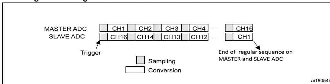
If DISCEN = 1 then each “n” simultaneous conversions of the regular sequence require a regular trigger event to occur (“n” is defined by DISCNUM).
This mode can be combined with AUTDLY mode:
- • Once a simultaneous conversion of the sequence has ended, the next conversion in the sequence is started only if the common data register, ADC12_CDR (or the regular data register of the master ADC) has been read (delay phase).
- • Once a simultaneous regular sequence of conversions has ended, a new regular trigger event is accepted only if the common data register (ADC12_CDR) has been read (delay phase). Any new regular trigger events occurring during the ongoing regular sequence and the associated delay phases are ignored.
It is possible to use the DMA to handle data in regular simultaneous mode combined with AUTDLY mode, assuming that multi-DMA mode is used: DAMDF[1:0] bits must be set to 10 or 11.
When regular simultaneous mode is combined with AUTDLY mode, it is mandatory for the user to ensure that:
- • The number of conversions in the master's sequence is equal to the number of conversions in the slave sequence.
- • For each simultaneous conversion of the sequence, the length of the conversion of the slave ADC is inferior to the length of the conversion of the master ADC. Note that the length of the sequence depends on the number of channels to convert and the sampling time and the resolution of each channel.
Note: This combination of regular simultaneous mode and AUTDLY mode is restricted to the use case when only regular channels are programmed: it is forbidden to program injected channels in this combined mode.
Interleaved mode with independent injected
This mode is selected by programming bits DUAL[4:0] = 00111.
This mode can be started only on a regular group (usually one channel). The external trigger source comes from the regular channel multiplexer of the master ADC.
After an external trigger occurs:
- • The master ADC starts immediately.
- • The slave ADC starts after a delay of several ADC clock cycles after the sampling phase of the master ADC has complete.
The minimum delay which separates two conversions in interleaved mode is configured in the DELAY bits in the ADC12_CCR register. This delay starts to count after the end of the sampling phase of the master conversion. This way, an ADC cannot start a conversion if the
complementary ADC is still sampling its input (only one ADC can sample the input signal at a given time).
- • The minimum possible DELAY is 1 to ensure that there is at least one cycle time between the opening of the analog switch of the master ADC sampling phase and the closing of the analog switch of the slave ADC sampling phase.
- • The maximum DELAY is equal to the number of cycles corresponding to the selected resolution. However, the user must properly calculate this delay to ensure that an ADC does not start a conversion while the other ADC is still sampling its input.
If the CONT bit is set on both master and slave ADCs, the selected regular channels of both ADCs are continuously converted.
The software is notified by interrupts when it can read the data at the end of each conversion event (EOC) on the slave ADC. A slave and master EOC interrupts are generated (if EOCIE is enabled) and the software can read the ADC_DR of the slave/master ADC.
Note: In 16-bit data format, enable only the slave EOC interrupt and read the common data register (ADC12_CDR). For 32-bit data format, enable both the slave and master EOC interrupts and read ADC12_CDR2 register. But in this case, the user must ensure that the duration of the conversions are compatible to ensure that inside the sequence, a master conversion is always followed by a slave conversion before a new master conversion restarts. It is recommended to use the MDMA mode.
It is also possible to have the regular data transferred by DMA. In this case, individual DMA requests on each ADC cannot be used and it is mandatory to use the DAMDF mode, as following:
- • Configure DAMDF[1:0] = 10 or 11 (depending on resolution).
- • A single DMA channel is used (the one of the masters). Configure the DMA master ADC channel to read the common ADC register (ADC12_CDR).
- • A single DMA request is generated each time both master and slave EOC events have occurred. At that time, the slave ADC converted data is available in the upper half-word of the ADC12_CDR 32-bit register and the master ADC converted data is available in the lower half-word of the ADC12_CDR register.
- • Both EOC flags are cleared when the DMA reads the ADC12_CCR register.
Figure 262. Interleaved mode on one channel in continuous conversion mode: dual ADC mode
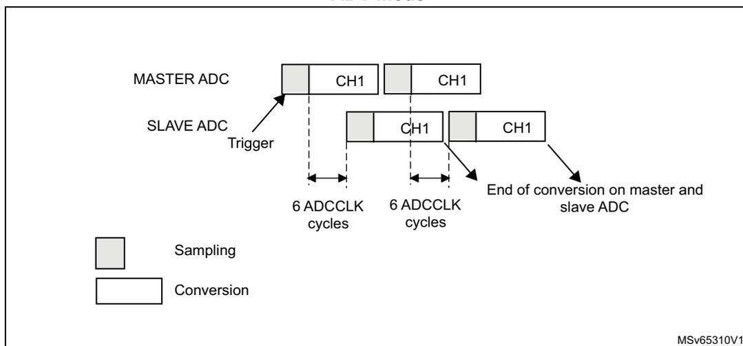
Figure 263. Interleaved mode on one channel in single conversion mode: dual ADC mode
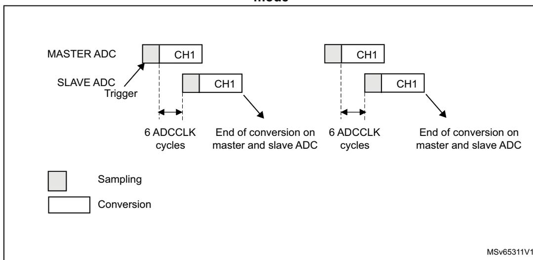
If DISCEN = 1, each “n” simultaneous conversions (“n” is defined by DISCNUM) of the regular sequence require a regular trigger event to occur.
In this mode, injected conversions are supported. When injection is done (either on master or on slave), both the master and the slave regular conversions are aborted and the sequence is restarted from the master (see Figure 264 below).
Figure 264. Interleaved conversion with injection
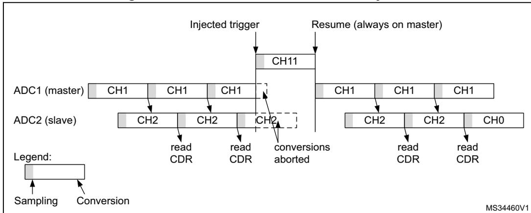
Alternate trigger mode
This mode is selected by programming bits DUAL[4:0] = 01001.
This mode can be started only on an injected group. The source of external trigger comes from the injected group multiplexer of the master ADC.
This mode is only possible when selecting hardware triggers: JEXTEN[1:0] must not be 0x0.
Injected discontinuous mode disabled (JDISCEN = 0 for both ADC)
- 1. When the 1st trigger occurs, all injected master ADC channels in the group are converted.
- 2. When the 2nd trigger occurs, all injected slave ADC channels in the group are converted.
- 3. And so on.
A JEOS interrupt, if enabled, is generated after all injected channels of the master ADC in the group have been converted.
A JEOS interrupt, if enabled, is generated after all injected channels of the slave ADC in the group have been converted.
JEOC interrupts, if enabled, can also be generated after each injected conversion.
If another external trigger occurs after all injected channels in the group have been converted then the alternate trigger process restarts by converting the injected channels of the master ADC in the group.
Figure 265. Alternate trigger: injected group of each ADC
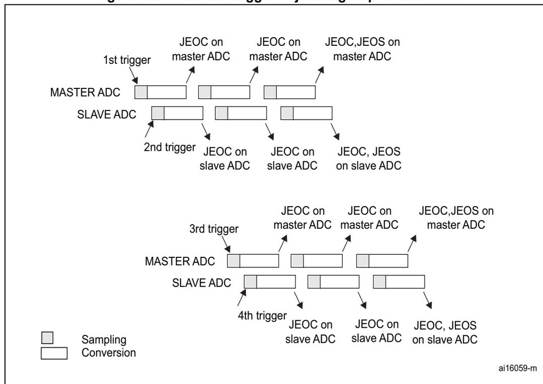
The diagram illustrates the timing of injected group conversions for a Master ADC and a Slave ADC, triggered by four external events (1st, 2nd, 3rd, and 4th triggers). The sequence of events is as follows:
- 1st trigger: Initiates the conversion of the first injected channel of the Master ADC.
- 2nd trigger: Initiates the conversion of the first injected channel of the Slave ADC.
- 3rd trigger: Initiates the conversion of the second injected channel of the Master ADC.
- 4th trigger: Initiates the conversion of the second injected channel of the Slave ADC.
For each injected channel, the Master ADC generates a JEOC interrupt upon completion. The Slave ADC also generates a JEOC interrupt upon completion. The Master ADC generates a JEOS interrupt after all injected channels in its group have been converted. The Slave ADC generates a JEOS interrupt after all injected channels in its group have been converted.
Legend:
- Sampling (represented by a shaded rectangle)
- Conversion (represented by a white rectangle)
ai16059-m
Note:
Regular conversions can be enabled on one or all ADCs. In this case, the regular conversions are independent of each other. A regular conversion is interrupted when the ADC has to perform an injected conversion. It is resumed when the injected conversion is finished.
The time interval between two trigger events must be greater than or equal to one ADC clock period. The minimum time interval between two trigger events that start conversions on the same ADC is the same as in the single ADC mode.
Injected discontinuous mode enabled (JDISCEN = 1 for both ADC)
If the injected discontinuous mode is enabled for both master and slave ADCs:
- • When the 1st trigger occurs, the first injected channel of the master ADC is converted.
- • When the 2nd trigger occurs, the first injected channel of the slave ADC is converted.
- • And so on.
A JEOS interrupt, if enabled, is generated after all injected channels of the master ADC in the group have been converted.
A JEOS interrupt, if enabled, is generated after all injected channels of the slave ADC in the group have been converted.
JEOC interrupts, if enabled, can also be generated after each injected conversions.
If another external trigger occurs after all injected channels in the group have been converted, then the alternate trigger process restarts.
Figure 266. Alternate trigger: Four injected channels (each ADC) in discontinuous mode
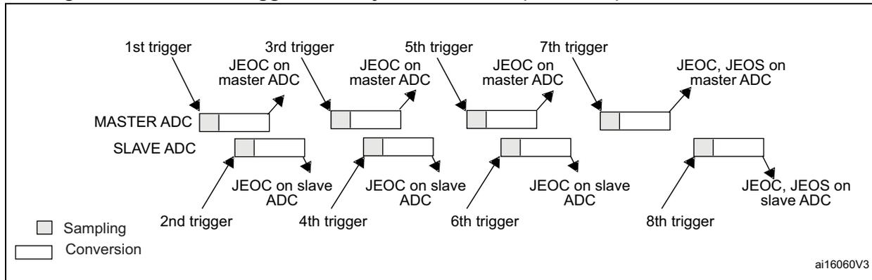
The diagram shows the timing of sampling and conversion for a Master ADC and a Slave ADC in discontinuous mode with alternate triggers. The Master ADC is triggered by the 1st, 3rd, 5th, and 7th triggers, while the Slave ADC is triggered by the 2nd, 4th, 6th, and 8th triggers. Each trigger initiates a sampling phase (small square) followed by a conversion phase (large rectangle). The Master ADC generates JEOC (End of Conversion) on master ADC after each conversion, and JEOC, JEOS (End of Sequence) on master ADC after the 4th conversion. The Slave ADC generates JEOC on slave ADC after each conversion, and JEOC, JEOS on slave ADC after the 4th conversion. The legend indicates that a small square represents Sampling and a large rectangle represents Conversion.
Combined regular/injected simultaneous mode
This mode is selected by programming bits DUAL[4:0] = 00001.
It is possible to interrupt the simultaneous conversion of a regular group to start the simultaneous conversion of an injected group.
Note: The sequences must be converted with the same length, the N-th conversion in master and slave mode must be configured with the same sampling time inside a given sequence, or the interval between triggers has to be longer than the long conversion time of the two sequences. If the above conditions are not respected, the ADC with the shortest sequence may restart while the ADC with the longest sequence is completing the previous conversions.
Combined regular simultaneous + alternate trigger mode
This mode is selected by programming bits DUAL[4:0] = 00010.
It is possible to interrupt the simultaneous conversion of a regular group to start the alternate trigger conversion of an injected group. Figure 267 shows the behavior of an alternate trigger interrupting a simultaneous regular conversion.
The injected alternate conversion is immediately started after the injected event. If a regular conversion is already running, in order to ensure synchronization after the injected conversion, the regular conversion of all (master/slave) ADCs is stopped and resumed synchronously at the end of the injected conversion.
Note: The sequences must be converted with the same length, the N-th conversion in master and slave mode must be configured with the same sampling time inside a given sequence, or the interval between triggers has to be longer than the long conversion time of the two sequences. If the above conditions are not respected, the ADC with the shortest sequence may restart while the ADC with the longest sequence is completing the previous conversions.
Figure 267. Alternate + regular simultaneous
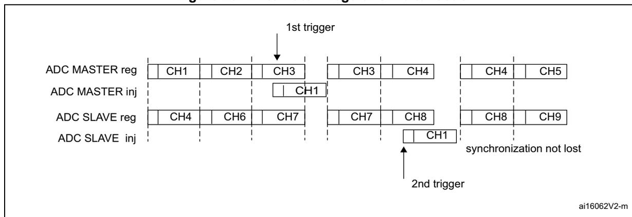
If a trigger occurs during an injected conversion that has interrupted a regular conversion, the alternate trigger is served. Figure 268 shows the behavior in this case (note that the 6th trigger is ignored because the associated alternate conversion is not complete).
Figure 268. Case of trigger occurring during injected conversion
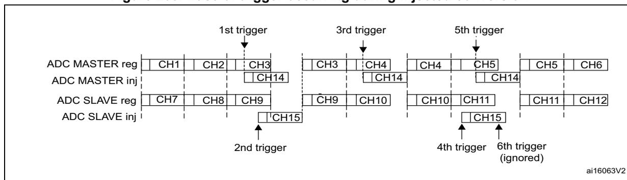
Combined injected simultaneous plus interleaved
This mode is selected by programming bits DUAL[4:0] = 00011.
It is possible to interrupt an interleaved conversion with a simultaneous injected event.
In this case the interleaved conversion is interrupted immediately and the simultaneous injected conversion starts. At the end of the injected sequence the interleaved conversion is resumed. When the interleaved regular conversion resumes, the first regular conversion which is performed is always the master's one. Figure 269, Figure 270 and Figure 271 show the behavior using an example.
Caution: In this mode, it is mandatory to use the Common Data Register to read the regular data with a single read access. On the contrary, master-slave data coherency is not guaranteed.
Figure 269. Interleaved single channel CH0 with injected sequence CH11, CH12
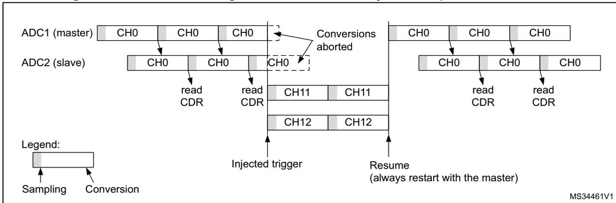
ADC1 (master) [CH0] [CH0] [CH0] ... [CH0] [CH0] [CH0]
ADC2 (slave) [CH0] [CH0] [CH0] ... [CH0] [CH0] [CH0]
read CDR
read CDR
Conversions aborted
Injected trigger
Resume (always restart with the master)
Legend:
Sampling Conversion
MS34461V1
Figure 270. Two interleaved channels (CH1, CH2) with injected sequence CH11, CH12 - case 1: Master interrupted first
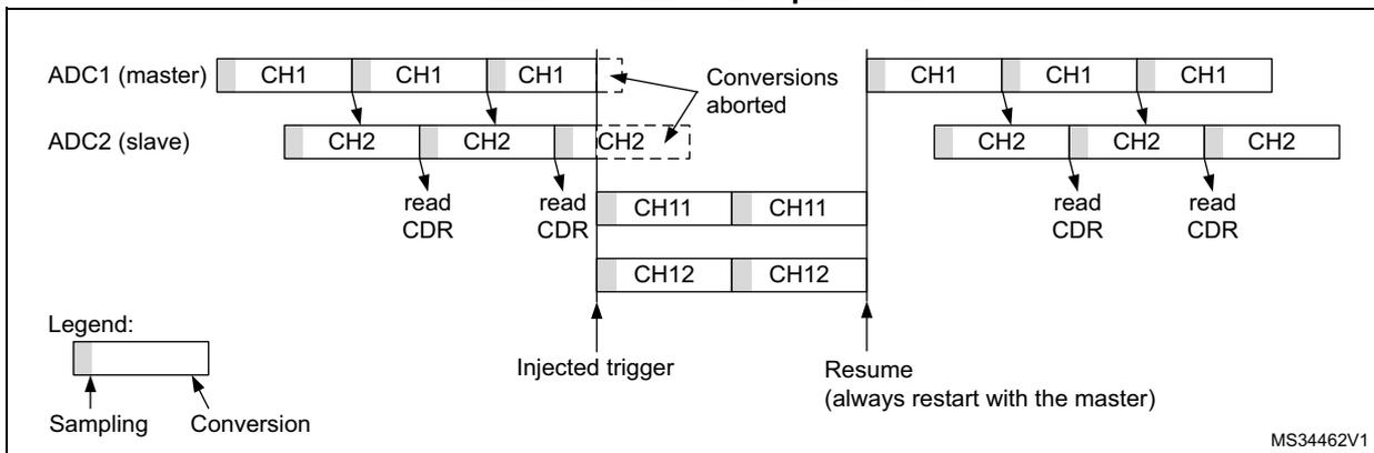
ADC1 (master) [CH1] [CH1] [CH1] ... [CH1] [CH1] [CH1]
ADC2 (slave) [CH2] [CH2] [CH2] ... [CH2] [CH2] [CH2]
read CDR
read CDR
Conversions aborted
Injected trigger
Resume (always restart with the master)
Legend:
Sampling Conversion
MS34462V1
Figure 271. Two Interleaved channels (CH1, CH2) with injected sequence CH11, CH12 - case 2: Slave interrupted first
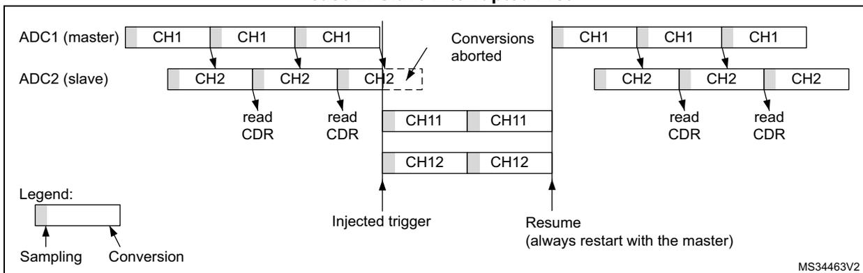
ADC1 (master) [CH1] [CH1] [CH1] ... [CH1] [CH1] [CH1]
ADC2 (slave) [CH2] [CH2] [CH2] ... [CH2] [CH2] [CH2]
read CDR
read CDR
Conversions aborted
Injected trigger
Resume (always restart with the master)
Legend:
Sampling Conversion
MS34463V2
DMA requests in dual ADC mode
In all dual ADC modes, it is possible to use two DMA channels (one for the master, one for the slave) to transfer the data, like in single mode (refer to Figure 272: DMA Requests in regular simultaneous mode when DAMDF[1:0] = 00 ).
Figure 272. DMA Requests in regular simultaneous mode when DAMDF[1:0] = 00
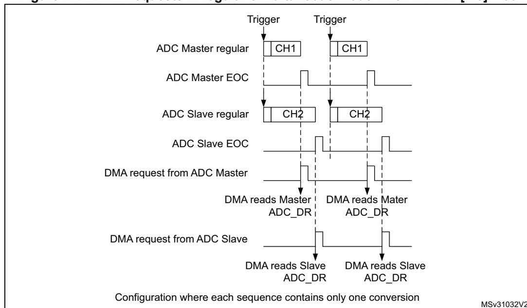
Configuration where each sequence contains only one conversion
MSV31032V2
In simultaneous regular and interleaved modes, it is also possible to save one DMA channel and transfer both data using a single DMA channel. For this the DAMDF[1:0] bits must be configured in the ADC12_CCR register:
- DAMDF[1:0] = 10, 32-bit format: A single DMA request is generated alternatively when either the master or slave EOC events have occurred. At that time, the data items are alternatively available in the ADC12_CDR2 32-bit register. This mode is used in interleaved mode and in regular simultaneous mode when resolution is above 16-bit.
Example:
Interleaved dual mode: a DMA request is generated each time a new 32-bit data is available:
1st DMA request: \( ADC12\_CDR2[31:0] = MST\_ADC\_DR[31:0] \)
2nd DMA request: \( ADC12\_CDR2[31:0] = SLV\_ADC\_DR[31:0] \)
- DAMDF[1:0] = 11, 16-bit format: A single DMA request is generated each time both master and slave EOC events have occurred. At that time, two data items are available and the 32-bit register ADC12_CDR contains the two half-words representing two
ADC-converted data items. The slave ADC data take the upper half-word and the master ADC data take the lower half-word.
This mode is used in interleaved mode and in regular simultaneous mode when resolution is ranging from 10 to 16-bit. Any value above 16-bit in the master or the slave converter is truncated to the least 16 significant bits.
Example:
Interleaved dual mode: a DMA request is generated each time 2 data items are available:
1st DMA request: \( ADC12\_CDR[31:0] = SLV\_ADC\_DR[15:0] \mid MST\_ADC\_DR[15:0] \)
2nd DMA request: \( ADC12\_CDR[31:0] = SLV\_ADC\_DR[15:0] \mid MST\_ADC\_DR[15:0] \)
Figure 273. DMA requests in regular simultaneous mode when DAMDF[1:0] = 10
Configuration where each sequence contains only one conversion
MSV31033V3
Figure 274. DMA requests in interleaved mode when DAMDF[1:0] = 10
Configuration where each sequence contains only one conversion
MSV31034V2
When using multiple-ADC mode, the user must take care to configure properly the duration of the master and slave conversions so that a DMA request is generated and served for reading both data (master + slave) before a new conversion is available.
- • DAMDF[1:0] = 11: This mode is similar to the DAMDF[1:0] = 10. The only differences are that on each DMA request (two data items are available), two bytes representing two ADC converted data items are transferred as a half-word.
This mode is used in interleaved and regular simultaneous mode when the result is 8-bit. A new DMA request is issued when four new 8-bit values are available.
Example:Interleaved dual mode: a DMA request is generated each time 2 data items are available
DMA request:
ADC12_CDR[7:0] = MST_ADC_DR[7:0]
ADC12_CDR[15:8] = SLV_ADC_DR[7:0]
ADC12_CDR[31:16] = 0x0
Overrun detectionIn dual ADC mode (when DUAL[4:0] is not equal to 0b00000), if an overrun is detected on one of the ADCs, the DMA requests are no longer issued to ensure that all the data transferred to the RAM are valid (this behavior occurs whatever the DAMDF configuration). It may happen that the EOC bit corresponding to one ADC remains set because the data register of this ADC contains valid data.
DMA one shot mode/ DMA circular mode when multiple-ADC mode is selectedWhen DAMDF mode is selected (10 or 11), bit DMNGT[1:0] = 10 in the master ADC ADC12_CCR register must also be configured to select between DMA one shot mode and circular mode, as explained in section Section : Managing conversions using the DMA .
Stopping the conversions in dual ADC modes
The user must set the control bits ADSTP/JADSTP of the master ADC to stop the conversions of both ADC in dual ADC mode. The other ADSTP control bit of the slave ADC has no effect in dual ADC mode.
Once both ADCs are effectively stopped, the bits ADSTART/JADSTART of the master and slave ADCs are both cleared by hardware.
MDF mode in dual ADC mode interleaved mode
In dual ADC interleaved modes, the ADC conversion results can be transferred directly to the multifunction digital filter (MDF).
This mode is enabled by setting the bits DMNGT[1:0] = 10 in the master ADC ADC_CFGR register.
The ADC transfers alternatively the 16 least significant bits of the regular data register from the master and the slave converter to a single channel of the MDF.
The data format must be 16-bit signed:
ADC_DR[31:16] = 0x0000
ADC_DR[15] = sign
ADC_DR[14:0] = data
Any value above 16-bit signed format in any converter is truncated.
MDF mode in dual ADC simultaneous mode
The dual mode is not required to use MDF in dual ADC simultaneous mode since conversion data are treated by each individual channel. Single mode with same trigger source results in simultaneous conversion with MDF interface.
33.4.32 Temperature sensor
The temperature sensor can measure the device junction temperature ( \( T_j \) ) in the \( -40 \) to \( 125 \) °C temperature range.
The temperature sensor is internally connected ADC input channels that are used to convert the sensor output voltage to a digital value (see Section 33.4.4: ADC connectivity for more details). The sampling time for the temperature sensor analog pin must be greater than the stabilization time specified in the device datasheet.
When it is not in use, the sensor can be placed in power-down mode.
Figure 275 shows the block diagram of the temperature sensor.
Figure 275. Temperature sensor channel block diagram
Reading the temperature
To use the sensor:
- 1. Select the input channels to which the temperature sensor is connected (with the appropriate sampling time).
- 2. Program with the appropriate sampling time (refer to electrical characteristics section of the device datasheet).
- 3. Set the VSENSESEL bit in the ADC12_CCR register to wake up the temperature sensor from power-down mode.
- 4. Start the ADC conversion.
- 5. Read the resulting data in the ADC data register.
- 6. Calculate the actual temperature using the following formula:
Where:
- – TS_CAL2 is the temperature sensor calibration value acquired at TS_CAL2_TEMP.
- – TS_CAL1 is the temperature sensor calibration value acquired at TS_CAL1_TEMP.
- – TS_DATA is the actual temperature sensor output value converted by ADC
Refer to Section 33.3: ADC implementation for more information on TS_CAL1 and TS_CAL2 calibration points.
Note: The sensor has a startup time after waking from power-down mode and before it can output at the correct level. The ADC also has a startup time after power-on. As a result, to minimize the delay, the ADEN and VSENSESEL bits must be set simultaneously.
33.4.33 \( V_{BAT} \) supply monitoring
The VBATEN bit in the ADC12_CCR register is used to switch to the battery voltage. As the \( V_{BAT} \) voltage can be higher than \( V_{DDA} \) , the VBAT pin is internally connected to a bridge divider by 4 to ensure the correct operation of the ADC. This bridge is automatically enabled when VBATEN is set, to connect \( V_{BAT}/4 \) to the corresponding ADC input channels (see Section 33.4.4: ADC connectivity for more details). As a consequence, the converted digital value is one fourth of the \( V_{BAT} \) voltage. To prevent any unwanted consumption on the battery, it is recommended to enable the bridge divider only when needed, for ADC conversion.
Refer to the electrical characteristics of the device datasheet for the sampling time value to be applied when converting the \( V_{BAT}/4 \) voltage.
Figure 276 shows the block diagram of the \( V_{BAT} \) sensing feature.
Figure 276. \( V_{BAT} \) channel block diagram
The diagram illustrates the internal circuitry for \( V_{BAT} \) monitoring. A VBAT pin is connected to a switch. This switch is controlled by the VBATEN control bit. When the switch is closed, it connects the VBAT pin to a bridge divider made of two resistors. The midpoint of this divider is labeled \( V_{BAT}/4 \) and is connected to an ADC input. The ADC input is part of an ADCx block, which is further connected to an Address/data bus. The bottom of the bridge divider is connected to ground.
Note: The VBATEN bit of the ADC12_CCR register must be set to enable the conversion of the ADC internal channels to which VBAT is connected (see Section 33.4.4: ADC connectivity for more details).
33.4.34 Monitoring the internal voltage reference
The internal voltage reference can be monitored to have a reference point for evaluating the ADC \( V_{REF+} \) voltage level.
Refer to Section 33.4.4: ADC connectivity for details on the ADC input channels to which the internal voltage reference is internally connected.
The sampling time for this channel must be greater than the stabilization time specified in the device datasheet.
Figure 276 shows the block diagram of the \( V_{REFINT} \) sensing feature.
Figure 277. V REFINT channel block diagram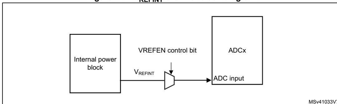
graph LR; IPB[Internal power block] -- VREFINT --> Switch; Switch --> ADCx[ADCx]; VREFEN[VREFEN control bit] --> Switch; Switch --> AI[ADC input];
Note: The VREFEN bit of the ADC12_CCR register must be set to enable the conversion of the ADC internal channels to which VREFINT is connected (see Section 33.4.4: ADC connectivity for more details).
Calculating the actual V REF+ voltage using the internal reference voltage
The V DDA power supply voltage applied to the microcontroller may be subject to variation or not precisely known. The embedded internal voltage reference (V REFINT ) and its calibration data acquired by the ADC during the manufacturing process at V REF+ = 3.0 V can be used to evaluate the actual V REF+ voltage level, if VREF+ pin is connected to a variable V DDA power supply.
The following formula gives the actual V REF+ voltage supplying the device:
Where:
- • VREFINT_CAL is the VREFINT calibration value (refer to Section 33.3: ADC implementation for the value of VREFINT_CAL).
- • VREFINT_DATA is the actual VREFINT output value converted by ADC.
Converting a supply-relative ADC measurement to an absolute voltage value
The ADC is designed to deliver a digital value corresponding to the ratio between the voltage reference \( V_{REF+} \) and the voltage applied on the converted channel. For most application use cases, it is necessary to convert this ratio into a voltage independent of \( V_{DDA} \) . For applications where \( V_{DDA} \) is known and ADC converted values are right-aligned, the following formula can be used to calculate this absolute value:
For applications where \( V_{DDA} \) value is not known, the internal voltage reference and \( V_{DDA} \) can be replaced by the expression provided in Section : Calculating the actual \( V_{REF+} \) voltage using the internal reference voltage , resulting in the following formula:
Where:
\( VREFINT\_CAL \) is the \( VREFINT \) calibration value (refer to Section 33.3: ADC implementation for the value of \( VREFINT\_CAL \) ).
\( ADC\_DATA \) is the value measured by the ADC on channel x (right-aligned)
\( VREFINT\_DATA \) is the actual \( VREFINT \) output value converted by the ADC
\( NUM\_CODES \) is the number of ADC output codes. For example with 14-bit resolution, it is \( 2^{14} = 16384 \) or with 8-bit resolution, \( 2^8 = 256 \) .
Note: If ADC measurements are done using an output format other than 14-bit right-aligned, all the parameters must first be converted to a compatible format before the calculation is done.
33.5 ADC interrupts
For each ADC, an interrupt can be generated:
- • After ADC power-up, when the ADC is ready (flag ADRDY)
- • On the end of any conversion for regular groups (flag EOC)
- • On the end of a sequence of conversion for regular groups (flag EOS)
- • On the end of any conversion for injected groups (flag JEOC)
- • On the end of a sequence of conversion for injected groups (flag JEOS)
- • When an analog watchdog detection occurs (flag AWD1, AWD2 and AWD3)
- • When the end of sampling phase occurs (flag EOSMP)
- • When the data overrun occurs (OVR flag)
Separate interrupt enable bits are available for flexibility.
Table 319. ADC interrupts
| Interrupt vector | Interrupt event | Event flag | Enable Control bit | Interrupt clear method | Exit from Sleep mode | Exit from Stop 0, Stop 1 and Stop 2 modes | Exit from Stop 3, Standby modes |
|---|---|---|---|---|---|---|---|
| ADC | ADC ready | ADRDY | ADRDYIE | Set by hardware and cleared by software | Yes | No | No |
| End of conversion of a regular group | EOC | EOCIE | |||||
| End of conversion sequence of a regular group | EOS | EOSIE | |||||
| End of conversion of an injected group | JEOC | JEOCIE | |||||
| End of conversion sequence of an injected group | JEOS | JEOSIE | |||||
| Analog watchdog 1 status bit is set | AWD1 | AWD1IE | |||||
| Analog watchdog 2 status bit is set | AWD2 | AWD2IE | |||||
| Analog watchdog 3 status bit is set | AWD3 | AWD3IE | |||||
| End of sampling phase | EOSMP | EOSMPIE | |||||
| Overrun | OVR | OVRIE |
33.6 ADC registers (for each ADC)
Refer to Section 1.2 for a list of abbreviations used in register descriptions.
33.6.1 ADC interrupt and status register (ADC_ISR)
Address offset: 0x00
Reset value: 0x0000 0000
| 31 | 30 | 29 | 28 | 27 | 26 | 25 | 24 | 23 | 22 | 21 | 20 | 19 | 18 | 17 | 16 |
|---|---|---|---|---|---|---|---|---|---|---|---|---|---|---|---|
| Res. | Res. | Res. | Res. | Res. | Res. | Res. | Res. | Res. | Res. | Res. | Res. | Res. | Res. | Res. | Res. |
| 15 | 14 | 13 | 12 | 11 | 10 | 9 | 8 | 7 | 6 | 5 | 4 | 3 | 2 | 1 | 0 |
| Res. | Res. | Res. | LDO RDY | Res. | Res. | AWD3 | AWD2 | AWD1 | JEOS | JEOC | OVR | EOS | EOC | EOSMP | ADRDY |
| r | rc_w1 | rc_w1 | rc_w1 | rc_w1 | rc_w1 | rc_w1 | rc_w1 | rc_w1 | rc_w1 | rc_w1 |
Bits 31:13 Reserved, must be kept at reset value.
Bit 12 LDORDY : ADC voltage regulator readyThis bit is set by hardware. It indicates that the ADC internal supply is ready. The ADC is available after \( t_{ADCVREG\_SETUP} \) time.
0: ADC voltage regulator disabled
1: ADC voltage regulator enabled
Bits 11:10 Reserved, must be kept at reset value.
Bit 9 AWD3 : Analog watchdog 3 flagThis bit is set by hardware when the converted voltage crosses the values programmed in the fields LT3[7:0] and HT3[7:0] of ADC_LTR3 & ADC_HTR3 register. It is cleared by software writing 1 to it.
0: No analog watchdog 3 event occurred (or the flag event was already acknowledged and cleared by software)
1: Analog watchdog 3 event occurred
Bit 8 AWD2 : Analog watchdog 2 flagThis bit is set by hardware when the converted voltage crosses the values programmed in the fields LT2[7:0] and HT2[7:0] of ADC_LTR2 & ADC_HTR2 register. It is cleared by software writing 1 to it.
0: No analog watchdog 2 event occurred (or the flag event was already acknowledged and cleared by software)
1: Analog watchdog 2 event occurred
Bit 7 AWD1 : Analog watchdog 1 flagThis bit is set by hardware when the converted voltage crosses the values programmed in the fields LT1[11:0] and HT1[11:0] of ADC_LTR1, & ADC_HTR1 register. It is cleared by software. writing 1 to it.
0: No analog watchdog 1 event occurred (or the flag event was already acknowledged and cleared by software)
1: Analog watchdog 1 event occurred
Bit 6 JEOS : Injected channel end of sequence flagThis bit is set by hardware at the end of the conversions of all injected channels in the group. It is cleared by software writing 1 to it.
0: Injected conversion sequence not complete (or the flag event was already acknowledged and cleared by software)
1: Injected conversions complete
Bit 5 JEOC : Injected channel end of conversion flagThis bit is set by hardware at the end of each injected conversion of a channel when a new data is available in the corresponding ADC_JDRy register. It is cleared by software writing 1 to it or by reading the corresponding ADC_JDRy register
0: Injected channel conversion not complete (or the flag event was already acknowledged and cleared by software)
1: Injected channel conversion complete
Bit 4 OVR : ADC overrunThis bit is set by hardware when an overrun occurs on a regular channel, meaning that a new conversion has completed while the EOC flag was already set. It is cleared by software writing 1 to it.
0: No overrun occurred (or the flag event was already acknowledged and cleared by software)
1: Overrun has occurred
Bit 3 EOS : End of regular sequence flag
This bit is set by hardware at the end of the conversions of a regular sequence of channels. It is cleared by software writing 1 to it.
0: Regular conversions sequence not complete (or the flag event was already acknowledged and cleared by software)
1: Regular conversions sequence complete
Bit 2 EOC : End of conversion flag
This bit is set by hardware at the end of each regular conversion of a channel when a new data is available in the ADC_DR register. It is cleared by software writing 1 to it or by reading the ADC_DR register
0: Regular channel conversion not complete (or the flag event was already acknowledged and cleared by software)
1: Regular channel conversion complete
Bit 1 EOSMP : End of sampling flag
This bit is set by hardware during the conversion of any channel (only for regular channels), at the end of the sampling phase.
0: not at the end of the sampling phase (or the flag event was already acknowledged and cleared by software)
1: End of sampling phase reached
Bit 0 ADRDY : ADC ready
This bit is set by hardware after the ADC has been enabled (bit ADEN = 1) and when the ADC reaches a state where it is ready to accept conversion requests.
It is cleared by software writing 1 to it.
0: ADC not yet ready to start conversion (or the flag event was already acknowledged and cleared by software)
1: ADC is ready to start conversion
33.6.2 ADC interrupt enable register (ADC_IER)
Address offset: 0x04
Reset value: 0x0000 0000
| 31 | 30 | 29 | 28 | 27 | 26 | 25 | 24 | 23 | 22 | 21 | 20 | 19 | 18 | 17 | 16 |
|---|---|---|---|---|---|---|---|---|---|---|---|---|---|---|---|
| Res. | Res. | Res. | Res. | Res. | Res. | Res. | Res. | Res. | Res. | Res. | Res. | Res. | Res. | Res. | Res. |
| 15 | 14 | 13 | 12 | 11 | 10 | 9 | 8 | 7 | 6 | 5 | 4 | 3 | 2 | 1 | 0 |
| Res. | Res. | Res. | Res. | Res. | Res. | AWD3 IE | AWD2 IE | AWD1 IE | JEOSIE | JEOCIE | OVRIE | EOSIE | EOCIE | EOSMP IE | ADRDY IE |
| rw | rw | rw | rw | rw | rw | rw | rw | rw | rw |
Bits 31:10 Reserved, must be kept at reset value.
Bit 9 AWD3IE : Analog watchdog 3 interrupt enable
This bit is set and cleared by software to enable/disable the analog watchdog 2 interrupt.
0: Analog watchdog 3 interrupt disabled
1: Analog watchdog 3 interrupt enabled
Note: Software is allowed to write this bit only when ADSTART = 0 and JADSTART = 0 (which ensures that no conversion is ongoing).
Bit 8 AWD2IE: Analog watchdog 2 interrupt enableThis bit is set and cleared by software to enable/disable the analog watchdog 2 interrupt.
0: Analog watchdog 2 interrupt disabled
1: Analog watchdog 2 interrupt enabled
Note: Software is allowed to write this bit only when ADSTART = 0 and JADSTART = 0 (which ensures that no conversion is ongoing).
Bit 7 AWD1IE: Analog watchdog 1 interrupt enableThis bit is set and cleared by software to enable/disable the analog watchdog 1 interrupt.
0: Analog watchdog 1 interrupt disabled
1: Analog watchdog 1 interrupt enabled
Note: Software is allowed to write this bit only when ADSTART = 0 and JADSTART = 0 (which ensures that no conversion is ongoing).
Bit 6 JEOSIE: End of injected sequence of conversions interrupt enableThis bit is set and cleared by software to enable/disable the end of injected sequence of conversions interrupt.
0: JEOS interrupt disabled
1: JEOS interrupt enabled. An interrupt is generated when the JEOS bit is set.
Note: Software is allowed to write this bit only when JADSTART = 0 (which ensures that no injected conversion is ongoing).
Bit 5 JEOCIE: End of injected conversion interrupt enableThis bit is set and cleared by software to enable/disable the end of an injected conversion interrupt.
0: JEOC interrupt disabled.
1: JEOC interrupt enabled. An interrupt is generated when the JEOC bit is set.
Note: Software is allowed to write this bit only when JADSTART = 0 (which ensures that no regular conversion is ongoing).
Bit 4 OVRIE: Overrun interrupt enableThis bit is set and cleared by software to enable/disable the Overrun interrupt of a regular conversion.
0: Overrun interrupt disabled
1: Overrun interrupt enabled. An interrupt is generated when the OVR bit is set.
Note: Software is allowed to write this bit only when ADSTART = 0 (which ensures that no regular conversion is ongoing).
Bit 3 EOSIE: End of regular sequence of conversions interrupt enableThis bit is set and cleared by software to enable/disable the end of regular sequence of conversions interrupt.
0: EOS interrupt disabled
1: EOS interrupt enabled. An interrupt is generated when the EOS bit is set.
Note: Software is allowed to write this bit only when ADSTART = 0 (which ensures that no regular conversion is ongoing).
Bit 2 EOCIE: End of regular conversion interrupt enableThis bit is set and cleared by software to enable/disable the end of a regular conversion interrupt.
0: EOC interrupt disabled.
1: EOC interrupt enabled. An interrupt is generated when the EOC bit is set.
Note: Software is allowed to write this bit only when ADSTART = 0 (which ensures that no regular conversion is ongoing).
Bit 1 EOSMPIE : End of sampling flag interrupt enable for regular conversions
This bit is set and cleared by software to enable/disable the end of the sampling phase interrupt for regular conversions.
0: EOSMP interrupt disabled.
1: EOSMP interrupt enabled. An interrupt is generated when the EOSMP bit is set.
Note: Software is allowed to write this bit only when ADSTART = 0 (which ensures that no regular conversion is ongoing).
Bit 0 ADRDYIE : ADC ready interrupt enable
This bit is set and cleared by software to enable/disable the ADC Ready interrupt.
0: ADRDY interrupt disabled
1: ADRDY interrupt enabled. An interrupt is generated when the ADRDY bit is set.
Note: Software is allowed to write this bit only when ADSTART = 0 and JADSTART = 0 (which ensures that no conversion is ongoing).
33.6.3 ADC control register (ADC_CR)
Address offset: 0x08
Reset value: 0x2000 0000
| 31 | 30 | 29 | 28 | 27 | 26 | 25 | 24 | 23 | 22 | 21 | 20 | 19 | 18 | 17 | 16 |
|---|---|---|---|---|---|---|---|---|---|---|---|---|---|---|---|
| ADCAL | Res. | DEEPPWD | ADVREG EN | CALINDEX[3:0] | Res. | Res. | Res. | Res. | Res. | Res. | Res. | ADCALLIN | |||
| rs | rw | rw | rw | rw | rw | rw | rw | ||||||||
| 15 | 14 | 13 | 12 | 11 | 10 | 9 | 8 | 7 | 6 | 5 | 4 | 3 | 2 | 1 | 0 |
| Res. | Res. | Res. | Res. | Res. | Res. | Res. | Res. | Res. | Res. | JADSTP | ADSTP | JADSTART | ADSTART | ADDIS | ADEN |
| rs | rs | rs | rs | rs | rs | ||||||||||
Bit 31 ADCAL : ADC calibration
This bit is set by software to start the ADC calibration.
It is cleared by hardware after calibration is complete.
0: Calibration complete
1: Write 1 to calibrate the ADC. Read at 1 means that a calibration in progress.
Note: The software is allowed to launch a calibration by setting ADCAL only when ADEN = 0.
Bit 30 Reserved, must be kept at reset value.
Bit 29 DEEPPWD : Deep-power-down enable
This bit is set and cleared by software to put the ADC in Deep-power-down mode.
0: ADC not in deep-power down
1: ADC in Deep-power-down (default reset state)
Note: The software is allowed to write this bit only when the ADC is disabled (ADCAL = 0, JADSTART = 0, JADSTP = 0, ADSTART = 0, ADSTP = 0, ADDIS = 0 and ADEN = 0).
Bit 28 ADVREGEN : ADC voltage regulator enable
This bit is set by software to enable the ADC voltage regulator.
Before performing any operation such as launching a calibration or enabling the ADC, the ADC voltage regulator must first be enabled and the software must wait for the regulator start-up time.
0: ADC Voltage regulator disabled
1: ADC Voltage regulator enabled.
For more details about the ADC voltage regulator enable and disable sequences, refer to
Section 33.4.6: ADC Deep-power-down mode (DEEPPWD) and ADC voltage regulator (ADVREGEN) .
The software can program this bitfield only when the ADC is disabled (ADCAL = 0, JADSTART = 0, ADSTART = 0, ADSTP = 0, ADDIS = 0 and ADEN = 0).
Bits 27:24 CALINDEX[3:0] : Calibration factor
This bitfield controls the calibration factor to be read or written.
Calibration index 0 is dedicated to single-ended and differential offsets, calibration index 1 to 7 to the linearity calibration factors, and index 8 to the internal offset:
0000: Offset calibration factor
0001: linearity calibration factor 1
0010: linearity calibration factor 2
0011: linearity calibration factor 3
0100: linearity calibration factor 4
0101: linearity calibration factor 5
0110: linearity calibration factor 6
0111: linearity calibration factor 7 and internal offset (write access only)
1000: internal offset (read access only)
1001: Calibration mode selection
Others: Reserved, must not be used
Note: ADC_CALFACT2[31:0] correspond to the location of CALINDEX[3:0] calibration factor data (see Section 33.4.8: Calibration (ADCAL, ADCALLIN, ADC_CALFACT) for details).
Bits 23:17 Reserved, must be kept at reset value.
Bit 16 ADCALLIN : Linearity calibration
This bit is set and cleared by software to enable the linearity calibration.
0: Writing ADCAL launches a calibration without the linearity calibration.
1: Writing ADCAL launches a calibration with the linearity calibration.
Note: The software is allowed to write this bit only when the ADC is disabled and is not calibrating (ADCAL = 0, JADSTART = 0, JADSTP = 0, ADSTART = 0, ADSTP = 0, ADDIS = 0 and ADEN = 0).
Bits 15:6 Reserved, must be kept at reset value.
Bit 5 JADSTP : ADC stop of injected conversion command
This bit is set by software to stop and discard an ongoing injected conversion (JADSTP Command). It is cleared by hardware when the conversion is effectively discarded and the ADC injected sequence and triggers can be re-configured. The ADC is then ready to accept a new start of injected conversions (JADSTART command).
0: No ADC stop injected conversion command ongoing
1: Write 1 to stop injected conversions ongoing. Read 1 means that an ADSTP command is in progress.
Note: The software is allowed to set JADSTP only when JADSTART = 1 and ADDIS = 0 (ADC is enabled and eventually converting an injected conversion and there is no pending request to disable the ADC).
In auto-injection mode (JAUTO = 1), setting ADSTP bit aborts both regular and injected conversions (do not use JADSTP)
Bit 4 ADSTP: ADC stop of regular conversion command
This bit is set by software to stop and discard an ongoing regular conversion (ADSTP Command). It is cleared by hardware when the conversion is effectively discarded and the ADC regular sequence and triggers can be re-configured. The ADC is then ready to accept a new start of regular conversions (ADSTART command).
0: No ADC stop regular conversion command ongoing
1: Write 1 to stop regular conversions ongoing. Read 1 means that an ADSTP command is in progress.
Note: The software is allowed to set ADSTP only when ADSTART = 1 and ADDIS = 0 (ADC is enabled and eventually converting a regular conversion and there is no pending request to disable the ADC).
In auto-injection mode (JAUTO = 1), setting ADSTP bit aborts both regular and injected conversions (do not use JADSTP).
Bit 3 JADSTART: ADC start of injected conversion
This bit is set by software to start ADC conversion of injected channels. Depending on the configuration bits JEXTEN[1:0], a conversion starts immediately (software trigger configuration) or once an injected hardware trigger event occurs (hardware trigger configuration).
It is cleared by hardware:
- – in single conversion mode when software trigger is selected (JEXTSEL = 0x0): at the assertion of the end of injected conversion sequence (JEOS) flag.
- – in all cases: after the execution of the JADSTP command, at the same time as JADSTP is cleared by hardware.
0: No ADC injected conversion is ongoing.
1: Write 1 to start injected conversions. Read 1 means that the ADC is operating and eventually converting an injected channel.
Note: The software is allowed to set JADSTART only when ADEN = 1 and ADDIS = 0 (ADC is enabled and there is no pending request to disable the ADC).
In auto-injection mode (JAUTO = 1), regular and auto-injected conversions are started by setting bit ADSTART (JADSTART must be kept cleared)
Bit 2 ADSTART: ADC start of regular conversion
This bit is set by software to start ADC conversion of regular channels. Depending on the configuration bits EXTEN[1:0], a conversion starts immediately (software trigger configuration) or once a regular hardware trigger event occurs (hardware trigger configuration).
It is cleared by hardware:
- – In single conversion mode (CONT = 0, DISCEN = 0) when software trigger is selected (EXTEN[1:0] = 0x0): at the assertion of the end of regular conversion sequence (EOS) flag.
- – In discontinuous conversion mode (CONT = 0, DISCEN = 1), when the software trigger is selected (EXTEN[1:0] = 0x0): at the end of conversion (EOC) flag.
- – in all other cases: after the execution of the ADSTP command, at the same time that ADSTP is cleared by hardware.
0: No ADC regular conversion is ongoing.
1: Write 1 to start regular conversions. Read 1 means that the ADC is operating and eventually converting a regular channel.
Note: The software is allowed to set ADSTART only when ADEN = 1 and ADDIS = 0 (ADC is enabled and there is no pending request to disable the ADC)
In auto-injection mode (JAUTO = 1), regular and auto-injected conversions are started by setting bit ADSTART (JADSTART must be kept cleared)
Bit 1 ADDIS : ADC disable command
This bit is set by software to disable the ADC (ADDIS command) and put it into power-down state (OFF state).
It is cleared by hardware once the ADC is effectively disabled (ADEN is also cleared by hardware at this time).
0: no ADDIS command ongoing
1: Write 1 to disable the ADC. Read 1 means that an ADDIS command is in progress.
Note: The software is allowed to set ADDIS only when ADEN = 1 and both ADSTART = 0 and JADSTART = 0 (which ensures that no conversion is ongoing)
Bit 0 ADEN : ADC enable control
This bit is set by software to enable the ADC. The ADC is effectively ready to operate once the flag ADRDY has been set.
It is cleared by hardware when the ADC is disabled, after the execution of the ADDIS command.
0: ADC is disabled (OFF state)
1: Write 1 to enable the ADC.
Note: The software is allowed to set ADEN only when all bits of ADC_CR registers are 0 (ADCAL = 0, JADSTART = 0, ADSTART = 0, ADSTP = 0, ADDIS = 0 and ADEN = 0) except for bit ADVREGEN which must be 1 (and the software must have wait for the startup time of the voltage regulator)
33.6.4 ADC configuration register (ADC_CFGR1)
Address offset: 0x0C
Reset value: 0x8000 0000
| 31 | 30 | 29 | 28 | 27 | 26 | 25 | 24 | 23 | 22 | 21 | 20 | 19 | 18 | 17 | 16 |
|---|---|---|---|---|---|---|---|---|---|---|---|---|---|---|---|
| Res. | AWD1CH[4:0] | JAUTO | JAWD1EN | AWD1EN | AWD1SGL | Res. | JDISCEN | DISCNUM[2:0] | DISCEN | ||||||
| rw | rw | rw | rw | rw | rw | rw | rw | rw | rw | rw | rw | rw | rw | ||
| 15 | 14 | 13 | 12 | 11 | 10 | 9 | 8 | 7 | 6 | 5 | 4 | 3 | 2 | 1 | 0 |
|---|---|---|---|---|---|---|---|---|---|---|---|---|---|---|---|
| Res. | AUTDLY | CONT | OVRMOD | EXTEN[1:0] | EXTSEL[4:0] | Res. | RES[1:0] | DMNGT[1:0] | |||||||
| rw | rw | rw | rw | rw | rw | rw | rw | rw | rw | rw | rw | rw | rw | ||
Bit 31 Reserved, must be kept at reset value.
Bits 30:26 AWD1CH[4:0] : Analog watchdog 1 channel selection
These bits are set and cleared by software. They select the input channel to be guarded by the analog watchdog.
00000: ADC analog input channel-0 monitored by AWD1
00001: ADC analog input channel-1 monitored by AWD1
.....
10011: ADC analog input channel-19 monitored by AWD1
Others: Reserved, must not be used
Note: The channel selected by AWD1CH must be also selected into the SQRI or JSQRI registers. Software is allowed to write these bits only when ADSTART = 0 and JADSTART = 0 (which ensures that no conversion is ongoing).
Bit 25 JAUTO: Automatic injected group conversionThis bit is set and cleared by software to enable/disable automatic injected group conversion after regular group conversion.
0: Automatic injected group conversion disabled
1: Automatic injected group conversion enabled
Note: The software is allowed to write this bit only when ADSTART = 0 and JADSTART = 0 (which ensures that no regular nor injected conversion is ongoing).
Bit 24 JAWD1EN: Analog watchdog 1 enable on injected channelsThis bit is set and cleared by software
0: Analog watchdog 1 disabled on injected channels
1: Analog watchdog 1 enabled on injected channels
Note: The software is allowed to write this bit only when JADSTART = 0 (which ensures that no injected conversion is ongoing).
Bit 23 AWD1EN: Analog watchdog 1 enable on regular channelsThis bit is set and cleared by software
0: Analog watchdog 1 disabled on regular channels
1: Analog watchdog 1 enabled on regular channels
Note: The software is allowed to write this bit only when ADSTART = 0 (which ensures that no regular conversion is ongoing).
Bit 22 AWD1SGL: Enable the watchdog 1 on a single channel or on all channelsThis bit is set and cleared by software to enable the analog watchdog on the channel identified by the AWD1CH[4:0] bits or on all the channels
0: Analog watchdog 1 enabled on all channels
1: Analog watchdog 1 enabled on a single channel
Note: The software is allowed to write these bits only when ADSTART = 0 and JADSTART = 0 (which ensures that no conversion is ongoing).
Bit 21 Reserved, must be kept at reset value. Bit 20 JDISCEN: Discontinuous mode on injected channelsThis bit is set and cleared by software to enable/disable discontinuous mode on the injected channels of a group.
0: Discontinuous mode on injected channels disabled
1: Discontinuous mode on injected channels enabled
Note: The software is allowed to write this bit only when JADSTART = 0 (which ensures that no injected conversion is ongoing).
It is not possible to use both auto-injected mode and discontinuous mode simultaneously: the bits DISCEN and JDISCEN must be kept cleared by software when JAUTO is set.
Bits 19:17 DISCNUM[2:0]: Discontinuous mode channel countThese bits are written by software to define the number of regular channels to be converted in discontinuous mode, after receiving an external trigger.
000: 1 channel
001: 2 channels
...
111: 8 channels
Note: The software is allowed to write these bits only when ADSTART = 0 (which ensures that no regular conversion is ongoing).
Bit 16 DISCEN: Discontinuous mode for regular channelsThis bit is set and cleared by software to enable/disable discontinuous mode for regular channels.
0: Discontinuous mode for regular channels disabled
1: Discontinuous mode for regular channels enabled
Note: It is not possible to have both discontinuous mode and continuous mode enabled: it is forbidden to set both DISCEN = 1 and CONT = 1.
It is not possible to use both auto-injected mode and discontinuous mode simultaneously: the bits DISCEN and JDISCEN must be kept cleared by software when JAUTO is set.
The software is allowed to write this bit only when ADSTART = 0 (which ensures that no regular conversion is ongoing).
Bit 15 Reserved, must be kept at reset value. Bit 14 AUTDLY: Delayed conversion modeThis bit is set and cleared by software to enable/disable the auto-delayed conversion mode.
0: Auto-delayed conversion mode off
1: Auto-delayed conversion mode on
Note: The software is allowed to write this bit only when ADSTART = 0 and JADSTART = 0 (which ensures that no conversion is ongoing).
Bit 13 CONT: Single / continuous conversion mode for regular conversionsThis bit is set and cleared by software. If it is set, regular conversion takes place continuously until it is cleared.
0: Single conversion mode
1: Continuous conversion mode
Note: It is not possible to have both discontinuous mode and continuous mode enabled: it is forbidden to set both DISCEN = 1 and CONT = 1.
The software is allowed to write this bit only when ADSTART = 0 (which ensures that no regular conversion is ongoing).
Bit 12 OVRMOD: Overrun ModeThis bit is set and cleared by software and configure the way data overrun is managed.
0: ADC_DR register is preserved with the old data when an overrun is detected.
1: ADC_DR register is overwritten with the last conversion result when an overrun is detected.
Note: The software is allowed to write this bit only when ADSTART = 0 (which ensures that no regular conversion is ongoing).
Bits 11:10 EXTEN[1:0]: External trigger enable and polarity selection for regular channelsThese bits are set and cleared by software to select the external trigger polarity and enable the trigger of a regular group.
00: Hardware trigger detection disabled (conversions can be launched by software)
01: Hardware trigger detection on the rising edge
10: Hardware trigger detection on the falling edge
11: Hardware trigger detection on both the rising and falling edges
Note: The software is allowed to write these bits only when ADSTART = 0 (which ensures that no regular conversion is ongoing).
Bits 9:5 EXTSEL[4:0] : External trigger selection for regular group
These bits select the external event used to trigger the start of conversion of a regular group:
00000: adc_ext_trg0
00001: adc_ext_trg1
...
Refer to the ADC external trigger for regular channels in Section 33.4.2: ADC pins and internal signals for details on trigger mapping.
Note: The software is allowed to write these bits only when ADSTART = 0 (which ensures that no regular conversion is ongoing).
Bit 4 Reserved, must be kept at reset value.
Bits 3:2 RES[1:0] : Data resolution
These bits are written by software to select the resolution of the conversion.
00: 14 bits
01: 12 bits
10: 10 bits
11: 8 bits
Note: The software is allowed to write these bits only when ADSTART = 0 and JADSTART = 0 (which ensures that no conversion is ongoing).
Bits 1:0 DMNGT[1:0] : Data management configuration
This bit is set and cleared by software to select how the ADC interface output data are managed.
00: Regular conversion data stored in DR only
01: DMA One-shot mode selected
10: MDF mode selected
11: DMA circular mode selected
Note: The software is allowed to write this bit only when ADSTART = 0 and JADSTART = 0 (which ensures that no conversion is ongoing).
33.6.5 ADC configuration register 2 (ADC_CFGR2)
Address offset: 0x10
Reset value: 0x0000 0000
| 31 | 30 | 29 | 28 | 27 | 26 | 25 | 24 | 23 | 22 | 21 | 20 | 19 | 18 | 17 | 16 |
|---|---|---|---|---|---|---|---|---|---|---|---|---|---|---|---|
| LSHIFT[3:0] | Res. | Res. | OSR[9:0] | ||||||||||||
| rw | rw | rw | rw | rw | rw | rw | rw | rw | rw | rw | rw | rw | rw | ||
| 15 | 14 | 13 | 12 | 11 | 10 | 9 | 8 | 7 | 6 | 5 | 4 | 3 | 2 | 1 | 0 |
| SMPTRIG | SWTRIG | BULB | Res. | Res. | ROVSM | TROVS | OVSS[3:0] | Res. | Res. | Res. | JOVSE | ||||
| rw | rw | rw | rw | rw | rw | rw | rw | rw | rw | rw | |||||
This bitfield is set and cleared by software to define the left shifting applied to the final result with or without oversampling.
0000: No left shift
0001: 1-bit left shift
0010: 2-bit left shift
0011: 3-bit left shift
0100: 4-bit left shift
0101: 5-bit left shift
0110: 6-bit left shift
0111: 7-bit left shift
1000: 8-bit left shift
1001: 9-bit left shift
1010: 10-bit left shift
1011: 11-bit left shift
1100: 12-bit left shift
1101: 13-bit left shift
1110: 14-bit left shift
1111: 15-bit left shift
Note: The software is allowed to write this bit only when ADSTART = 0 (which ensures that no conversion is ongoing).
Bits 27:26 Reserved, must be kept at reset value.
Bits 25:16 OSR[9:0] : Oversampling ratioThis bitfield is set and cleared by software to define the oversampling ratio.
0: 1x (no oversampling)
1: 2x
2: 3x
...
1023: 1024x
Note: The software is allowed to write this bit only when ADSTART = 0 (which ensures that no conversion is ongoing).
Bit 15 SMPTRIG : Sampling time control trigger modeThis bit is set and cleared by software to enable the sampling time control trigger mode.
0: Sampling time control trigger mode disabled
1: Sampling time control trigger mode enabled
The sampling time starts on the trigger rising edge, and the conversion on the trigger falling edge.
EXTEN[1:0] bits must be set to 01. BULB bit must not be set when the SMPTRIG bit is set.
When EXTEN[1:0] bits is set to 00, set SWTRIG to start the sampling and clear SWTRIG bit to start the conversion.
Note: The software is allowed to write this bit only when ADSTART = 0 (which ensures that no conversion is ongoing).
Bit 14 SWTRIG : Software trigger bit for sampling time control trigger modeThis bit is set and cleared by software to enable the bulb sampling mode.
0: Software trigger starts the conversion for sampling time control trigger mode
1: Software trigger starts the sampling for sampling time control trigger mode.
Note: The software is allowed to write this bit only when ADSTART = 0 (which ensures that no conversion is ongoing).
Bit 13 BULB : Bulb sampling modeThis bit is set and cleared by software to select the bulb sampling mode.
0: Bulb sampling mode disabled
1: Bulb sampling mode enabled. The sampling period starts just after the previous end of the conversion.
SMPTRIG bit must not be set when the BULB bit is set.
The very first ADC conversion is performed with the sampling time specified in SMPx bits.
Note: The software is allowed to write this bit only when ADSTART = 0 (which ensures that no conversion is ongoing).
Bits 12:11 Reserved, must be kept at reset value.
Bit 10 ROVSM : Regular oversampling modeThis bit is set and cleared by software to select the regular oversampling mode.
0: Continued mode: When injected conversions are triggered, the oversampling is temporary stopped and continued after the injection sequence (oversampling buffer is maintained during injected sequence)
1: Resumed mode: When injected conversions are triggered, the current oversampling is aborted and resumed from start after the injection sequence (oversampling buffer is zeroed by injected sequence start)
Note: The software is allowed to write this bit only when ADSTART = 0 (which ensures that no conversion is ongoing).
Bit 9 TROVS : Triggered regular oversamplingThis bit is set and cleared by software to enable triggered oversampling
0: All oversampled conversions for a channel are done consecutively following a trigger
1: Each oversampled conversion for a channel needs a new trigger
Note: The software is allowed to write this bit only when ADSTART = 0 (which ensures that no conversion is ongoing).
Bits 8:5 OVSS[3:0] : Oversampling right shiftThis bitfield is set and cleared by software to define the right shifting applied to the raw oversampling result.
0000: No right shift
0001: 1-bit right shift
0010: 2-bit right shift
0011: 3-bit right shift
0100: 4-bit right shift
0101: 5-bit right shift
0110: 6-bit right shift
0111: 7-bit right shift
1000: 8-bit right shift
1001: 9-bit right shift
1010: 10-bit right shift
Others: Reserved, must not be used.
Note: The software is allowed to write these bits only when ADSTART = 0 (which ensures that no conversion is ongoing).
Bits 4:2 Reserved, must be kept at reset value.
Bit 1 JOVSE : Injected oversampling enable
This bit is set and cleared by software to enable injected oversampling.
0: Injected oversampling disabled
1: Injected oversampling enabled
Note: The software is allowed to write this bit only when ADSTART = 0 and JADSTART = 0 (which ensures that no conversion is ongoing)
Bit 0 ROVSE : Regular oversampling enable
This bit is set and cleared by software to enable regular oversampling.
0: Regular oversampling disabled
1: Regular oversampling enabled
Note: The software is allowed to write this bit only when ADSTART = 0 and JADSTART = 0 (which ensures that no conversion is ongoing)
33.6.6 ADC sample time register 1 (ADC_SMPR1)
Address offset: 0x14
Reset value: 0x0000 0000
| 31 | 30 | 29 | 28 | 27 | 26 | 25 | 24 | 23 | 22 | 21 | 20 | 19 | 18 | 17 | 16 |
|---|---|---|---|---|---|---|---|---|---|---|---|---|---|---|---|
| Res. | Res. | SMP9[2:0] | SMP8[2:0] | SMP7[2:0] | SMP6[2:0] | SMP5[2:1] | |||||||||
| rw | rw | rw | rw | rw | rw | rw | rw | rw | rw | rw | rw | rw | rw | ||
| 15 | 14 | 13 | 12 | 11 | 10 | 9 | 8 | 7 | 6 | 5 | 4 | 3 | 2 | 1 | 0 |
| SMP5[0] | SMP4[2:0] | SMP3[2:0] | SMP2[2:0] | SMP1[2:0] | SMP0[2:0] | ||||||||||
| rw | rw | rw | rw | rw | rw | rw | rw | rw | rw | rw | rw | rw | rw | rw | rw |
Bits 31:30 Reserved, must be kept at reset value.
Bits 29:0 SMPx[2:0] : Channel x sampling time selection (x = 9 to 0)
These bits are written by software to select the sampling time individually for each channel.
During sample cycles, the channel selection bits must remain unchanged.
000: 5 ADC clock cycles
001: 6 ADC clock cycles
010: 12 ADC clock cycles
011: 20 ADC clock cycles
100: 36 ADC clock cycles
101: 68 ADC clock cycles
110: 391 ADC clock cycles
111: 814 ADC clock cycles
Note: The software is allowed to write these bits only when ADSTART = 0 and JADSTART = 0 (which ensures that no conversion is ongoing).
33.6.7 ADC sample time register 2 (ADC_SMPR2)
Address offset: 0x18
Reset value: 0x0000 0000
| 31 | 30 | 29 | 28 | 27 | 26 | 25 | 24 | 23 | 22 | 21 | 20 | 19 | 18 | 17 | 16 |
|---|---|---|---|---|---|---|---|---|---|---|---|---|---|---|---|
| Res. | Res. | SMP19[2:0] | SMP18[2:0] | SMP17[2:0] | SMP16[2:0] | SMP15[2:1] | |||||||||
| rw | rw | rw | rw | rw | rw | rw | rw | rw | rw | rw | rw | rw | rw | ||
| 15 | 14 | 13 | 12 | 11 | 10 | 9 | 8 | 7 | 6 | 5 | 4 | 3 | 2 | 1 | 0 |
| SMP15[0] | SMP14[2:0] | SMP13[2:0] | SMP12[2:0] | SMP11[2:0] | SMP10[2:0] | ||||||||||
| rw | rw | rw | rw | rw | rw | rw | rw | rw | rw | rw | rw | rw | rw | rw | rw |
Bits 31:30 Reserved, must be kept at reset value.
Bits 29:0 SMPx[2:0] : Channel x sampling time selection (x = 19 to 10)
These bits are written by software to select the sampling time individually for each channel. During sampling cycles, the channel selection bits must remain unchanged.
000: 5 ADC clock cycles
001: 6 ADC clock cycles
010: 12 ADC clock cycles
011: 20 ADC clock cycles
100: 36 ADC clock cycles
101: 68 ADC clock cycles
110: 391 ADC clock cycles
111: 814 ADC clock cycles
Note: The software is allowed to write these bits only when ADSTART = 0 and JADSTART = 0 (which ensures that no conversion is ongoing).
33.6.8 ADC channel preselection register (ADC_PCSEL)
Address offset: 0x1C
Reset value: 0x0000 0000
| 31 | 30 | 29 | 28 | 27 | 26 | 25 | 24 | 23 | 22 | 21 | 20 | 19 | 18 | 17 | 16 |
|---|---|---|---|---|---|---|---|---|---|---|---|---|---|---|---|
| Res. | Res. | Res. | Res. | Res. | Res. | Res. | Res. | Res. | Res. | Res. | Res. | PCSEL1 9 | PCSEL1 8 | PCSEL1 7 | PCSEL1 6 |
| rw | rw | rw | rw | ||||||||||||
| 15 | 14 | 13 | 12 | 11 | 10 | 9 | 8 | 7 | 6 | 5 | 4 | 3 | 2 | 1 | 0 |
| PCSEL L15 | PCSEL L14 | PCSEL L13 | PCSEL L12 | PCSEL L11 | PCSEL L10 | PCSEL 9 | PCSEL 8 | PCSEL 7 | PCSEL 6 | PCSEL 5 | PCSEL 4 | PCSEL3 | PCSEL2 | PCSEL1 | PCSEL0 |
| rw | rw | rw | rw | rw | rw | rw | rw | rw | rw | rw | rw | rw | rw | rw | rw |
Bits 31:20 Reserved, must be kept at reset value.
Bits 19:0 PCSEL[19:0] : Channel i ( \( V_{INP}[i] \) ) preselection
These bits are written by software to preselect the input channel I/O instance to be converted.
0: Input channel i ( \( V_{INP}[i] \) ) is not preselected for conversion, the ADC conversion of this channel shows a wrong result.
1: Input channel i ( \( V_{INP}[i] \) ) is preselected for conversion
Note: The software is allowed to write these bits only when ADSTART = 0 and JADSTART = 0 (which ensures that no conversion is ongoing).
33.6.9 ADC regular sequence register 1 (ADC_SQR1)
Address offset: 0x30
Reset value: 0x0000 0000
| 31 | 30 | 29 | 28 | 27 | 26 | 25 | 24 | 23 | 22 | 21 | 20 | 19 | 18 | 17 | 16 |
|---|---|---|---|---|---|---|---|---|---|---|---|---|---|---|---|
| Res. | Res. | Res. | SQ4[4:0] | Res. | SQ3[4:0] | Res. | SQ2[4] | ||||||||
| rw | rw | rw | rw | rw | rw | rw | rw | rw | rw | rw | |||||
| 15 | 14 | 13 | 12 | 11 | 10 | 9 | 8 | 7 | 6 | 5 | 4 | 3 | 2 | 1 | 0 |
| SQ2[3:0] | Res. | SQ1[4:0] | Res. | Res. | L[3:0] | ||||||||||
| rw | rw | rw | rw | rw | rw | rw | rw | rw | rw | rw | rw | rw | |||
Bits 31:29 Reserved, must be kept at reset value.
Bits 28:24 SQ4[4:0] : 4th conversion in regular sequence
These bits are written by software with the channel number (0..19) assigned as the 4th in the regular conversion sequence.
Bit 23 Reserved, must be kept at reset value.
Bits 22:18 SQ3[4:0] : 3rd conversion in regular sequence
These bits are written by software with the channel number (0..19) assigned as the 3rd in the regular conversion sequence.
Note: The software is allowed to write these bits only when ADSTART = 0 (which ensures that no regular conversion is ongoing).
Bit 17 Reserved, must be kept at reset value.
Bits 16:12 SQ2[4:0] : 2nd conversion in regular sequence
These bits are written by software with the channel number (0..19) assigned as the 2nd in the regular conversion sequence.
Note: The software is allowed to write these bits only when ADSTART = 0 (which ensures that no regular conversion is ongoing).
Bit 11 Reserved, must be kept at reset value.
Bits 10:6 SQ1[4:0] : 1st conversion in regular sequence
These bits are written by software with the channel number (0..19) assigned as the 1st in the regular conversion sequence.
Note: The software is allowed to write these bits only when ADSTART = 0 (which ensures that no regular conversion is ongoing).
Bits 5:4 Reserved, must be kept at reset value.
Bits 3:0 L[3:0] : Regular channel sequence length
These bits are written by software to define the total number of conversions in the regular channel conversion sequence.
0000: 1 conversion
0001: 2 conversions
...
1111: 16 conversions
Note: The software is allowed to write these bits only when ADSTART = 0 (which ensures that no regular conversion is ongoing).
33.6.10 ADC regular sequence register 2 (ADC_SQR2)
Address offset: 0x34
Reset value: 0x0000 0000
| 31 | 30 | 29 | 28 | 27 | 26 | 25 | 24 | 23 | 22 | 21 | 20 | 19 | 18 | 17 | 16 |
|---|---|---|---|---|---|---|---|---|---|---|---|---|---|---|---|
| Res. | Res. | Res. | SQ9[4:0] | Res. | SQ8[4:0] | Res. | SQ7[4] | ||||||||
| rw | rw | rw | rw | rw | rw | rw | rw | rw | |||||||
| 15 | 14 | 13 | 12 | 11 | 10 | 9 | 8 | 7 | 6 | 5 | 4 | 3 | 2 | 1 | 0 |
| SQ7[3:0] | Res. | SQ6[4:0] | Res. | SQ5[4:0] | |||||||||||
| rw | rw | rw | rw | rw | rw | rw | rw | rw | rw | rw | rw | rw | rw | rw | |
Bits 31:29 Reserved, must be kept at reset value.
Bits 28:24 SQ9[4:0] : 9th conversion in regular sequence
These bits are written by software with the channel number (0..19) assigned as the 9th in the regular conversion sequence.
Note: The software is allowed to write these bits only when ADSTART = 0 (which ensures that no regular conversion is ongoing).
Bit 23 Reserved, must be kept at reset value.
Bits 22:18 SQ8[4:0] : 8th conversion in regular sequence
These bits are written by software with the channel number (0..19) assigned as the 8th in the regular conversion sequence
Note: The software is allowed to write these bits only when ADSTART = 0 (which ensures that no regular conversion is ongoing).
Bit 17 Reserved, must be kept at reset value.
Bits 16:12 SQ7[4:0] : 7th conversion in regular sequence
These bits are written by software with the channel number (0..19) assigned as the 7th in the regular conversion sequence.
Note: The software is allowed to write these bits only when ADSTART = 0 (which ensures that no regular conversion is ongoing).
Bit 11 Reserved, must be kept at reset value.
Bits 10:6 SQ6[4:0] : 6th conversion in regular sequence
These bits are written by software with the channel number (0..19) assigned as the 6th in the regular conversion sequence.
Note: The software is allowed to write these bits only when ADSTART = 0 (which ensures that no regular conversion is ongoing).
Bit 5 Reserved, must be kept at reset value.
Bits 4:0 SQ5[4:0] : 5th conversion in regular sequence
These bits are written by software with the channel number (0..19) assigned as the 5th in the regular conversion sequence.
Note: The software is allowed to write these bits only when ADSTART = 0 (which ensures that no regular conversion is ongoing).
33.6.11 ADC regular sequence register 3 (ADC_SQR3)
Address offset: 0x38
Reset value: 0x0000 0000
| 31 | 30 | 29 | 28 | 27 | 26 | 25 | 24 | 23 | 22 | 21 | 20 | 19 | 18 | 17 | 16 |
|---|---|---|---|---|---|---|---|---|---|---|---|---|---|---|---|
| Res. | Res. | Res. | SQ14[4:0] | Res. | SQ13[4:0] | Res. | SQ12[4] | ||||||||
| rw | rw | rw | rw | rw | rw | rw | rw | rw | rw | rw | |||||
| 15 | 14 | 13 | 12 | 11 | 10 | 9 | 8 | 7 | 6 | 5 | 4 | 3 | 2 | 1 | 0 |
|---|---|---|---|---|---|---|---|---|---|---|---|---|---|---|---|
| SQ12[3:0] | Res. | SQ11[4:0] | Res. | SQ10[4:0] | |||||||||||
| rw | rw | rw | rw | rw | rw | rw | rw | rw | rw | rw | rw | rw | rw | ||
Bits 31:29 Reserved, must be kept at reset value.
Bits 28:24 SQ14[4:0] : 14th conversion in regular sequence
These bits are written by software with the channel number (0..19) assigned as the 14th in the regular conversion sequence.
Note: The software is allowed to write these bits only when ADSTART = 0 (which ensures that no regular conversion is ongoing).
Bit 23 Reserved, must be kept at reset value.
Bits 22:18 SQ13[4:0] : 13th conversion in regular sequence
These bits are written by software with the channel number (0..19) assigned as the 13th in the regular conversion sequence.
Note: The software is allowed to write these bits only when ADSTART = 0 (which ensures that no regular conversion is ongoing).
Bit 17 Reserved, must be kept at reset value.
Bits 16:12 SQ12[4:0] : 12th conversion in regular sequence
These bits are written by software with the channel number (0..19) assigned as the 12th in the regular conversion sequence.
Note: The software is allowed to write these bits only when ADSTART = 0 (which ensures that no regular conversion is ongoing).
Bit 11 Reserved, must be kept at reset value.
Bits 10:6 SQ11[4:0] : 11th conversion in regular sequence
These bits are written by software with the channel number (0..19) assigned as the 11th in the regular conversion sequence.
Note: The software is allowed to write these bits only when ADSTART = 0 (which ensures that no regular conversion is ongoing).
Bit 5 Reserved, must be kept at reset value.
Bits 4:0 SQ10[4:0] : 10th conversion in regular sequence
These bits are written by software with the channel number (0..19) assigned as the 10th in the regular conversion sequence.
Note: The software is allowed to write these bits only when ADSTART = 0 (which ensures that no regular conversion is ongoing).
33.6.12 ADC regular sequence register 4 (ADC_SQR4)
Address offset: 0x3C
Reset value: 0x0000 0000
| 31 | 30 | 29 | 28 | 27 | 26 | 25 | 24 | 23 | 22 | 21 | 20 | 19 | 18 | 17 | 16 |
|---|---|---|---|---|---|---|---|---|---|---|---|---|---|---|---|
| Res. | Res. | Res. | Res. | Res. | Res. | Res. | Res. | Res. | Res. | Res. | Res. | Res. | Res. | Res. | Res. |
| 15 | 14 | 13 | 12 | 11 | 10 | 9 | 8 | 7 | 6 | 5 | 4 | 3 | 2 | 1 | 0 |
| Res. | Res. | Res. | Res. | Res. | SQ16[4:0] | Res. | SQ15[4:0] | ||||||||
| rw | rw | rw | rw | rw | rw | rw | rw | rw | rw | ||||||
Bits 31:11 Reserved, must be kept at reset value.
Bits 10:6 SQ16[4:0] : 16th conversion in regular sequence
These bits are written by software with the channel number (0..19) assigned as the 16th in the regular conversion sequence.
Note: The software is allowed to write these bits only when ADSTART = 0 (which ensures that no regular conversion is ongoing).
Bit 5 Reserved, must be kept at reset value.
Bits 4:0 SQ15[4:0] : 15th conversion in regular sequence
These bits are written by software with the channel number (0..19) assigned as the 15th in the regular conversion sequence.
Note: The software is allowed to write these bits only when ADSTART = 0 (which ensures that no regular conversion is ongoing).
33.6.13 ADC regular data register (ADC_DR)
Address offset: 0x40
Reset value: 0x0000 0000
| 31 | 30 | 29 | 28 | 27 | 26 | 25 | 24 | 23 | 22 | 21 | 20 | 19 | 18 | 17 | 16 |
|---|---|---|---|---|---|---|---|---|---|---|---|---|---|---|---|
| RDATA[31:16] | |||||||||||||||
| r | r | r | r | r | r | r | r | r | r | r | r | r | r | r | r |
| 15 | 14 | 13 | 12 | 11 | 10 | 9 | 8 | 7 | 6 | 5 | 4 | 3 | 2 | 1 | 0 |
| RDATA[15:0] | |||||||||||||||
| r | r | r | r | r | r | r | r | r | r | r | r | r | r | r | r |
Bits 31:0 RDATA[31:0] : Regular data converted
These bits are read-only. They contain the conversion result from the last converted regular channel. The data are left- or right-aligned as described in Section 33.4.26: Data management .
33.6.14 ADC injected sequence register (ADC_JSQR)
Address offset: 0x4C
Reset value: 0x0000 0000
| 31 | 30 | 29 | 28 | 27 | 26 | 25 | 24 | 23 | 22 | 21 | 20 | 19 | 18 | 17 | 16 |
|---|---|---|---|---|---|---|---|---|---|---|---|---|---|---|---|
| JSQ4[4:0] | Res. | JSQ3[4:0] | Res. | JSQ2[4:1] | |||||||||||
| rw | rw | rw | rw | rw | rw | rw | rw | rw | rw | rw | rw | rw | rw | ||
| 15 | 14 | 13 | 12 | 11 | 10 | 9 | 8 | 7 | 6 | 5 | 4 | 3 | 2 | 1 | 0 |
| JSQ2[0] | Res. | JSQ1[4:0] | JEXTEN[1:0] | JEXTSEL[4:0] | JL[1:0] | ||||||||||
| rw | rw | rw | rw | rw | rw | rw | rw | rw | rw | rw | rw | rw | rw | rw | |
Bits 31:27 JSQ4[4:0] : 4th conversion in the injected sequence
These bits are written by software with the channel number (0..19) assigned as the 4th in the injected conversion sequence.
Note: The software is allowed to write these bits only when JADSTART = 0 (which ensures that no injected conversion is ongoing).
Bit 26 Reserved, must be kept at reset value.
Bits 25:21 JSQ3[4:0] : 3rd conversion in the injected sequence
These bits are written by software with the channel number (0..19) assigned as the 3rd in the injected conversion sequence.
Note: The software is allowed to write these bits only when JADSTART = 0 (which ensures that no injected conversion is ongoing).
Bit 20 Reserved, must be kept at reset value.
Bits 19:15 JSQ2[4:0] : 2nd conversion in the injected sequence
These bits are written by software with the channel number (0..19) assigned as the 2nd in the injected conversion sequence.
Note: The software is allowed to write these bits only when JADSTART = 0 (which ensures that no injected conversion is ongoing).
Bit 14 Reserved, must be kept at reset value.
Bits 13:9 JSQ1[4:0] : 1st conversion in the injected sequence
These bits are written by software with the channel number (0..19) assigned as the 1st in the injected conversion sequence.
Note: The software is allowed to write these bits only when JADSTART = 0 (which ensures that no injected conversion is ongoing).
Bits 8:7 JEXTEN[1:0] : External trigger enable and polarity selection for injected channels
These bits are set and cleared by software to select the external trigger polarity and enable the trigger of an injected group.
00: Hardware trigger detection disabled (conversions can be launched by software)
01: Hardware trigger detection on the rising edge
10: Hardware trigger detection on the falling edge
11: Hardware trigger detection on both the rising and falling edges
Note: The software is allowed to write these bits only when JADSTART = 0 (which ensures that no injected conversion is ongoing).
Bits 6:2 JEXTSEL[4:0] : External trigger selection for injected group
These bits select the external event used to trigger the start of conversion of an injected group:
00000: adc_jext_trg0
00001: adc_jext_trg1
...
Refer to the ADC external trigger for injected channels in Section 33.4.2: ADC pins and internal signals for details on trigger mapping.
Note: The software is allowed to write these bits only when JADSTART = 0 (which ensures that no injected conversion is ongoing).
Bits 1:0 JL[1:0] : Injected channel sequence length
These bits are written by software to define the total number of conversions in the injected channel conversion sequence.
00: 1 conversion
01: 2 conversions
10: 3 conversions
11: 4 conversions
Note: The software is allowed to write these bits only when JADSTART = 0 (which ensures that no injected conversion is ongoing).
33.6.15 ADC offset y register (ADC_OFRy)
Address offset: \( 0x60 + 0x04 * (y - 1) \) , ( \( y = 1 \) to 4)
Reset value: 0x0000 0000
| 31 | 30 | 29 | 28 | 27 | 26 | 25 | 24 | 23 | 22 | 21 | 20 | 19 | 18 | 17 | 16 |
|---|---|---|---|---|---|---|---|---|---|---|---|---|---|---|---|
| OFFSET_CH[4:0] | SSAT | USAT | POSOFF | OFFSET[23:16] | |||||||||||
| rw | rw | rw | rw | rw | rw | rw | rw | rw | rw | rw | rw | rw | rw | rw | rw |
| 15 | 14 | 13 | 12 | 11 | 10 | 9 | 8 | 7 | 6 | 5 | 4 | 3 | 2 | 1 | 0 |
| OFFSET[15:0] | |||||||||||||||
| rw | rw | rw | rw | rw | rw | rw | rw | rw | rw | rw | rw | rw | rw | rw | rw |
Bits 31:27 OFFSET_CH[4:0] : Channel selection for the data offset y
These bits are written by software to define the channel to which the offset programmed into OFFSETy[25:0] bits applies.
Note: The software is allowed to write these bits only when ADSTART = 0 and JADSTART = 0 (which ensures that no conversion is ongoing).
If OFFSETy_EN bit is set, it is not allowed to select the same channel in different ADC_OFRy registers.
Bit 26 SSAT : Signed saturation enable
This bit is written by software to enable or disable the Signed saturation feature.
(see Section : Data register, data alignment and offset (ADC_DR, ADC_JDRy, OFFSETy, OFFSETy_CH, OVSS, LSHIFT, USAT, SSAT) for details).
0: Offset is subtracted maintaining data integrity and extending converted data size (9-bit and 15-bit signed format).
1: Offset is subtracted and result is saturated to maintain converted data size.
Note: The software is allowed to write this bit only when ADSTART = 0 and JADSTART = 0 (which ensures that no conversion is ongoing).
Bit 25 USAT : Unsigned saturation enable
This bit is written by software to enable or disable the unsigned saturation feature.
0: Offset is subtracted maintaining data integrity and keeping converted data size
1: Offset is subtracted and result is saturated to maintain converted data size.
Note: The software is allowed to write this bit only when ADSTART = 0 and JADSTART = 0 (which ensures that no conversion is ongoing).
Bit 24 POSOFF : offset sign
This bit is set and cleared by software to enable the positive offset.
0: Negative offset
1: Positive offset
Note: The software is allowed to write these bits only when ADSTART = 0 and JADSTART = 0 (which ensures that no conversion is ongoing).
Bits 23:0 OFFSET[23:0] : Data offset y for the channel programmed into OFFSETy_CH[4:0] bits
These bits are written by software to define the offset y to be subtracted from the raw converted data when converting a channel (regular or injected). The channel to which the data offset y applies must be programmed to the OFFSETy_CH[4:0] bits. The conversion result can be read from in the ADC_DR (regular conversion) or from in the ADC_JDRyi registers (injected conversion).
When OFFSETy[21:0] bitfield is reset, the offset compensation is disabled.
Note: The software is allowed to write these bits only when ADSTART = 0 and JADSTART = 0 (which ensures that no conversion is ongoing).
If several offsets (OFFSETy) point to the same channel, only the offset with the lowest y value is considered for the subtraction.
For example, if OFFSET1_CH[4:0] = 4 and OFFSET2_CH[4:0] = 4, this is OFFSET1[25:0] that is subtracted when converting channel 4.
33.6.16 ADC gain compensation register (ADC_GCOMP)
Address offset: 0x70
Reset value: 0x0000 0000
| 31 | 30 | 29 | 28 | 27 | 26 | 25 | 24 | 23 | 22 | 21 | 20 | 19 | 18 | 17 | 16 |
|---|---|---|---|---|---|---|---|---|---|---|---|---|---|---|---|
| GCOMP | Res. | Res. | Res. | Res. | Res. | Res. | Res. | Res. | Res. | Res. | Res. | Res. | Res. | Res. | Res. |
| rw |
| 15 | 14 | 13 | 12 | 11 | 10 | 9 | 8 | 7 | 6 | 5 | 4 | 3 | 2 | 1 | 0 |
|---|---|---|---|---|---|---|---|---|---|---|---|---|---|---|---|
| Res. | Res. | GCOMPCOEFF[13:0] | |||||||||||||
| rw | rw | rw | rw | rw | rw | rw | rw | rw | rw | rw | rw | rw | rw | ||
Bit 31 GCOMP : Gain compensation mode
This bit is set and cleared by software to enable the gain compensation mode.
0: Regular ADC operating mode
1: Gain compensation enabled and applied on all channels
Note: The software is allowed to write this bit only when ADSTART = 0 (which ensures that no conversion is ongoing).
Bits 30:14 Reserved, must be kept at reset value.
Bits 13:0 GCOMPcoeff[13:0] : Gain compensation coefficient
These bits are set and cleared by software to program the gain compensation coefficient.
00 1000 0000 0000: gain factor of 0.5
...
01 0000 0000 0000: gain factor of 1
10 0000 0000 0000: gain factor of 2
11 0000 0000 0000: gain factor of 3
...
The coefficient is divided by 4096 to get the gain factor ranging from 0 to 3.999756.
Note: This gain compensation is only applied when GCOMP bit of ADCx_CFG2 register is 1.
33.6.17 ADC injected data register (ADC_JDRy)
Address offset: 0x80 + 0x04 * (y - 1), (y= 1 to 4)
Reset value: 0x0000 0000
| 31 | 30 | 29 | 28 | 27 | 26 | 25 | 24 | 23 | 22 | 21 | 20 | 19 | 18 | 17 | 16 |
|---|---|---|---|---|---|---|---|---|---|---|---|---|---|---|---|
| JDATA[31:16] | |||||||||||||||
| r | r | r | r | r | r | r | r | r | r | r | r | r | r | r | r |
| 15 | 14 | 13 | 12 | 11 | 10 | 9 | 8 | 7 | 6 | 5 | 4 | 3 | 2 | 1 | 0 |
| JDATA[15:0] | |||||||||||||||
| r | r | r | r | r | r | r | r | r | r | r | r | r | r | r | r |
Bits 31:0 JDATA[31:0] : Injected data
These bits are read-only. They contain the conversion result from injected channel y. The data are left -or right-aligned as described in Section 33.4.26: Data management .
33.6.18 ADC analog watchdog 2 configuration register (ADC_AWD2CR)
Address offset: 0xA0
Reset value: 0x0000 0000
| 31 | 30 | 29 | 28 | 27 | 26 | 25 | 24 | 23 | 22 | 21 | 20 | 19 | 18 | 17 | 16 |
|---|---|---|---|---|---|---|---|---|---|---|---|---|---|---|---|
| Res. | Res. | Res. | Res. | Res. | Res. | Res. | Res. | Res. | Res. | Res. | Res. | AWD2CH[19:16] | |||
| rw | rw | rw | rw | ||||||||||||
| 15 | 14 | 13 | 12 | 11 | 10 | 9 | 8 | 7 | 6 | 5 | 4 | 3 | 2 | 1 | 0 |
| AWD2CH[15:0] | |||||||||||||||
| rw | rw | rw | rw | rw | rw | rw | rw | rw | rw | rw | rw | rw | rw | rw | rw |
Bits 31:20 Reserved, must be kept at reset value.
Bits 19:0 AWD2CH[19:0] : Analog watchdog 2 channel selection
These bits are set and cleared by software. They enable and select the input channels to be guarded by the analog watchdog 2.
AWD2CH[i] = 0: ADC analog input channel-i is not monitored by AWD2
AWD2CH[i] = 1: ADC analog input channel-i is monitored by AWD2
When AWD2CH[19:0] = 000..0, the analog Watchdog 2 is disabled
Note: The channels selected by AWD2CH must be also selected into the SQRi or JSQRi registers.
Software is allowed to write these bits only when ADSTART = 0 and JADSTART = 0 (which ensures that no conversion is ongoing).
33.6.19 ADC analog watchdog 3 configuration register (ADC_AWD3CR)
Address offset: 0xA4
Reset value: 0x0000 0000
| 31 | 30 | 29 | 28 | 27 | 26 | 25 | 24 | 23 | 22 | 21 | 20 | 19 | 18 | 17 | 16 |
|---|---|---|---|---|---|---|---|---|---|---|---|---|---|---|---|
| Res. | Res. | Res. | Res. | Res. | Res. | Res. | Res. | Res. | Res. | Res. | Res. | AWD3CH[19:16] | |||
| rw | rw | rw | rw | ||||||||||||
| 15 | 14 | 13 | 12 | 11 | 10 | 9 | 8 | 7 | 6 | 5 | 4 | 3 | 2 | 1 | 0 |
| AWD3CH[15:0] | |||||||||||||||
| rw | rw | rw | rw | rw | rw | rw | rw | rw | rw | rw | rw | rw | rw | rw | rw |
Bits 31:20 Reserved, must be kept at reset value.
Bits 19:0 AWD3CH[19:0] : Analog watchdog 3 channel selection
These bits are set and cleared by software. They enable and select the input channels to be guarded by the analog watchdog 3.
AWD3CH[i] = 0: ADC analog input channel-i is not monitored by AWD3
AWD3CH[i] = 1: ADC analog input channel-i is monitored by AWD3
When AWD3CH[19:0] = 000..0, the analog Watchdog 3 is disabled
Note: The channels selected by AWD3CH must be also selected into the SQRi or JSQRi registers.
The software is allowed to write these bits only when ADSTART = 0 and JADSTART = 0 (which ensures that no conversion is ongoing).
33.6.20 ADC watchdog threshold register 1 (ADC_LTR1)
Address offset: 0xA8
Reset value: 0x0000 0000
| 31 | 30 | 29 | 28 | 27 | 26 | 25 | 24 | 23 | 22 | 21 | 20 | 19 | 18 | 17 | 16 |
|---|---|---|---|---|---|---|---|---|---|---|---|---|---|---|---|
| Res. | Res. | Res. | Res. | Res. | Res. | Res. | LTR1[24:16] | ||||||||
| rw | rw | rw | rw | rw | rw | rw | rw | rw | |||||||
| 15 | 14 | 13 | 12 | 11 | 10 | 9 | 8 | 7 | 6 | 5 | 4 | 3 | 2 | 1 | 0 |
| LTR1[15:0] | |||||||||||||||
| rw | rw | rw | rw | rw | rw | rw | rw | rw | rw | rw | rw | rw | rw | rw | rw |
Bits 31:25 Reserved, must be kept at reset value.
Bits 24:0 LTR1[24:0] : Analog watchdog 1 lower threshold
These bits are written by software to define the lower threshold for the analog watchdog 1.
33.6.21 ADC watchdog threshold register 1 (ADC_HTR1)
Address offset: 0xAC
Reset value: 0x01FF FFFF
| 31 | 30 | 29 | 28 | 27 | 26 | 25 | 24 | 23 | 22 | 21 | 20 | 19 | 18 | 17 | 16 |
|---|---|---|---|---|---|---|---|---|---|---|---|---|---|---|---|
| AWDFILT1[2:0] | Res. | Res. | Res. | Res. | HTR1[24:16] | ||||||||||
| rw | rw | rw | rw | rw | rw | rw | rw | rw | rw | rw | rw | ||||
| 15 | 14 | 13 | 12 | 11 | 10 | 9 | 8 | 7 | 6 | 5 | 4 | 3 | 2 | 1 | 0 |
| HTR1[15:0] | |||||||||||||||
| rw | rw | rw | rw | rw | rw | rw | rw | rw | rw | rw | rw | rw | rw | rw | rw |
Bits 31:29 AWDFILT1[2:0] : Analog watchdog filtering parameter
This bit is set and cleared by software.
000: No filtering
001: two consecutive detection generates an AWDx flag or an interrupt
...
111: Eight consecutive detection generates an AWDx flag or an interrupt
Note: The software is allowed to write this bit only when ADSTART = 0 and JADSTART = 0 (which ensures that no conversion is ongoing).
Bits 28:25 Reserved, must be kept at reset value.
Bits 24:0 HTR1[24:0] : Analog watchdog 1 higher threshold
These bits are written by software to define the higher threshold for the analog watchdog 1.
33.6.22 ADC watchdog lower threshold register 2 (ADC_LTR2)
Address offset: 0xB0
Reset value: 0x0000 0000
| 31 | 30 | 29 | 28 | 27 | 26 | 25 | 24 | 23 | 22 | 21 | 20 | 19 | 18 | 17 | 16 |
|---|---|---|---|---|---|---|---|---|---|---|---|---|---|---|---|
| Res. | Res. | Res. | Res. | Res. | Res. | Res. | LTR2[24:16] | ||||||||
| rw | rw | rw | rw | rw | rw | rw | rw | rw | |||||||
| 15 | 14 | 13 | 12 | 11 | 10 | 9 | 8 | 7 | 6 | 5 | 4 | 3 | 2 | 1 | 0 |
| LTR2[15:0] | |||||||||||||||
| rw | rw | rw | rw | rw | rw | rw | rw | rw | rw | rw | rw | rw | rw | rw | rw |
Bits 31:25 Reserved, must be kept at reset value.
Bits 24:0 LTR2[24:0] : Analog watchdog 2 lower threshold
These bits are written by software to define the lower threshold for the analog watchdog 2.
33.6.23 ADC watchdog higher threshold register 2 (ADC_HTR2)
Address offset: 0xB4
Reset value: 0x01FF FFFF
| 31 | 30 | 29 | 28 | 27 | 26 | 25 | 24 | 23 | 22 | 21 | 20 | 19 | 18 | 17 | 16 |
|---|---|---|---|---|---|---|---|---|---|---|---|---|---|---|---|
| Res. | Res. | Res. | Res. | Res. | Res. | Res. | HTR2[24:16] | ||||||||
| rw | rw | rw | rw | rw | rw | rw | rw | rw | |||||||
| 15 | 14 | 13 | 12 | 11 | 10 | 9 | 8 | 7 | 6 | 5 | 4 | 3 | 2 | 1 | 0 |
| HTR2[15:0] | |||||||||||||||
| rw | rw | rw | rw | rw | rw | rw | rw | rw | rw | rw | rw | rw | rw | rw | rw |
Bits 31:25 Reserved, must be kept at reset value.
Bits 24:0 HTR2[24:0] : Analog watchdog 2 higher threshold
These bits are written by software to define the higher threshold for the analog watchdog 2.
33.6.24 ADC watchdog lower threshold register 3 (ADC_LTR3)
Address offset: 0xB8
Reset value: 0x0000 0000
| 31 | 30 | 29 | 28 | 27 | 26 | 25 | 24 | 23 | 22 | 21 | 20 | 19 | 18 | 17 | 16 |
|---|---|---|---|---|---|---|---|---|---|---|---|---|---|---|---|
| Res. | Res. | Res. | Res. | Res. | Res. | Res. | LTR3[24:16] | ||||||||
| rw | rw | rw | rw | rw | rw | rw | rw | rw | |||||||
| 15 | 14 | 13 | 12 | 11 | 10 | 9 | 8 | 7 | 6 | 5 | 4 | 3 | 2 | 1 | 0 |
| LTR3[15:0] | |||||||||||||||
| rw | rw | rw | rw | rw | rw | rw | rw | rw | rw | rw | rw | rw | rw | rw | rw |
Bits 31:25 Reserved, must be kept at reset value.
Bits 24:0 LTR3[24:0] : Analog watchdog 3 lower threshold
These bits are written by software to define the lower threshold for the analog watchdog 3.
33.6.25 ADC watchdog higher threshold register 3 (ADC_HTR3)
Address offset: 0xBC
Reset value: 0x01FF FFFF
| 31 | 30 | 29 | 28 | 27 | 26 | 25 | 24 | 23 | 22 | 21 | 20 | 19 | 18 | 17 | 16 |
|---|---|---|---|---|---|---|---|---|---|---|---|---|---|---|---|
| Res. | Res. | Res. | Res. | Res. | Res. | Res. | HTR3[24:16] | ||||||||
| rw | rw | rw | rw | rw | rw | rw | rw | rw | |||||||
| 15 | 14 | 13 | 12 | 11 | 10 | 9 | 8 | 7 | 6 | 5 | 4 | 3 | 2 | 1 | 0 |
| HTR3[15:0] | |||||||||||||||
| rw | rw | rw | rw | rw | rw | rw | rw | rw | rw | rw | rw | rw | rw | rw | rw |
Bits 31:25 Reserved, must be kept at reset value.
Bits 24:0 HTR3[24:0] : Analog watchdog 3 higher threshold
These bits are written by software to define the higher threshold for the analog watchdog 3.
33.6.26 ADC differential mode selection register (ADC_DIFSEL)
Address offset: 0xC0
Reset value: 0x0000 0000
| 31 | 30 | 29 | 28 | 27 | 26 | 25 | 24 | 23 | 22 | 21 | 20 | 19 | 18 | 17 | 16 |
|---|---|---|---|---|---|---|---|---|---|---|---|---|---|---|---|
| Res. | Res. | Res. | Res. | Res. | Res. | Res. | Res. | Res. | Res. | Res. | Res. | DIFSEL[19:16] | |||
| rw | rw | rw | rw | ||||||||||||
| 15 | 14 | 13 | 12 | 11 | 10 | 9 | 8 | 7 | 6 | 5 | 4 | 3 | 2 | 1 | 0 |
| DIFSEL[15:0] | |||||||||||||||
| rw | rw | rw | rw | rw | rw | rw | rw | rw | rw | rw | rw | rw | rw | rw | rw |
Bits 31:20 Reserved, must be kept at reset value.
Bits 19:0 DIFSEL[19:0] : Differential mode for channels 19 to 0
These bits are set and cleared by software. They allow selecting if a channel is configured as single-ended or differential mode.
DIFSEL[i] = 0: ADC analog input channel-i is configured in single-ended mode
DIFSEL[i] = 1: ADC analog input channel-i is configured in differential mode
Note: The software is allowed to write these bits only when the ADC is disabled (ADCAL = 0, JADSTART = 0, JADSTP = 0, ADSTART = 0, ADSTP = 0, ADDIS = 0 and ADEN = 0).
33.6.27 ADC user control register (ADC_CALFACT)
Address offset: 0xC4
Reset value: 0x0000 0000
| 31 | 30 | 29 | 28 | 27 | 26 | 25 | 24 | 23 | 22 | 21 | 20 | 19 | 18 | 17 | 16 |
|---|---|---|---|---|---|---|---|---|---|---|---|---|---|---|---|
| Res. | Res. | Res. | Res. | Res. | Res. | CAPTURE _COEF | LATCH _COEF | Res. | Res. | Res. | Res. | Res. | Res. | Res. | VALIDITY |
| rw | rw | r |
| 15 | 14 | 13 | 12 | 11 | 10 | 9 | 8 | 7 | 6 | 5 | 4 | 3 | 2 | 1 | 0 |
|---|---|---|---|---|---|---|---|---|---|---|---|---|---|---|---|
| I_APB_DATA[7:0] | I_APB_ADDR[7:0] | ||||||||||||||
| r | r | r | r | r | r | r | r | r | r | r | r | r | r | r | r |
Bits 31:26 Reserved, must be kept at reset value.
Bit 25 CAPTURE_COEF : Calibration factor capture enable bit
- This bit enables the internal calibration factor capture.
- 0: Calibration factor not captured
- 1: Calibration factor available in CALFACT[31:0] bits, the calibration factor index being defined by CALINDEX[3:0] bits
Bit 24 LATCH_COEF : Calibration factor latch enable bit
- This bit latches the calibration factor in the CALFACT[31:0] bits.
- 0: No effect
- 1: Calibration factor latched in the analog block on LATCH_COEF bit transition from 0 to 1. Prior to latching the calibration factor, CALFACT[31:0] bits must be programmed with the content of CALINDEX[3:0] bits.
Bits 23:17 Reserved, must be kept at reset value.
Bit 16 VALIDITY : Delayed write access status bit
- This bit indicates the communication status between the ADC digital and analog blocks.
- 0: Operation still in progress
- 1: Operation complete
Bits 15:8 I_APB_DATA[7:0] : Delayed write access data
This bitfield contains the data that are being written during delayed write accesses.
Bits 7:0 I_APB_ADDR[7:0] : Delayed write access address
This bitfield contains the address that is being written during delayed write accesses.
33.6.28 ADC calibration factor register (ADC_CALFACT2)
Address offset: 0xC8
Reset value: 0x0000 0000
| 31 | 30 | 29 | 28 | 27 | 26 | 25 | 24 | 23 | 22 | 21 | 20 | 19 | 18 | 17 | 16 |
|---|---|---|---|---|---|---|---|---|---|---|---|---|---|---|---|
| CALFACT[31:16] | |||||||||||||||
| rw | rw | rw | rw | rw | rw | rw | rw | rw | rw | rw | rw | rw | rw | rw | rw |
| 15 | 14 | 13 | 12 | 11 | 10 | 9 | 8 | 7 | 6 | 5 | 4 | 3 | 2 | 1 | 0 |
|---|---|---|---|---|---|---|---|---|---|---|---|---|---|---|---|
| CALFACT[15:0] | |||||||||||||||
| rw | rw | rw | rw | rw | rw | rw | rw | rw | rw | rw | rw | rw | rw | rw | rw |
Bits 31:0 CALFACT[31:0] : Linearity or offset calibration factor
These bits can be written either by hardware or by software.
They contain the 32-bit offset or linearity calibration factor.
When CAPTURE_COEF is set, the calibration factor of the analog block is read back and stored in CALFACT[31:0], indexed by CALINDEX[3:0] bits.
When LATCH_COEF is set, the calibration factor of the analog block is updated with the value programmed in CALFACT[31:0], indexed by CALINDEX[3:0] bits.
To read all calibration factors, perform nine accesses to the ADC_CALFACT2 register.
To write all calibration factors, perform eight accesses to the ADC_CALFACT2 register.
Note: The software is allowed to write these bits only when ADEN = 1, ADSTART = 0 and JADSTART = 0 (ADC is enabled and no calibration is ongoing and no conversion is ongoing).
33.7 ADC common registers
These registers define the control and status registers common to master and slave ADCs.
33.7.1 ADC common status register (ADC12_CSR)
Address offset: 0x00
Reset value: 0x0000 0000
The address offset is relative to the master ADC base address + 0x300.
This register provides an image of the status bits of the different ADCs. Nevertheless, it is read-only and does not clear the different status bits. Instead, each status bit must be cleared by writing 1 to it in the corresponding ADC_ISR register.
ADC1 and ADC2 are controlled by the same interface.
This register is available only the devices that support dual mode (see Section 33.3: ADC implementation ).
| 31 | 30 | 29 | 28 | 27 | 26 | 25 | 24 | 23 | 22 | 21 | 20 | 19 | 18 | 17 | 16 |
|---|---|---|---|---|---|---|---|---|---|---|---|---|---|---|---|
| Res. | Res. | Res. | LDORDY _SLV | Res. | Res. | AWD3 _SLV | AWD2 _SLV | AWD1 _SLV | JEOS _SLV | JEOC _SLV | OVR _SLV | EOS _SLV | EOC _SLV | EOSMP _SLV | ADRDY _SLV |
| r | r | r | r | r | r | r | r | r | r | r | |||||
| 15 | 14 | 13 | 12 | 11 | 10 | 9 | 8 | 7 | 6 | 5 | 4 | 3 | 2 | 1 | 0 |
| Res. | Res. | Res. | LDORDY _MST | Res. | Res. | AWD3 _MST | AWD2 _MST | AWD1 _MST | JEOS _MST | JEOC _MST | OVR _MST | EOS _MST | EOC _MST | EOSMP _MST | ADRDY _MST |
| r | r | r | r | r | r | r | r | r | r | r |
Bits 31:29 Reserved, must be kept at reset value.
Bit 28 LDORDY_SLV : ADC voltage regulator ready flag of the slave ADC
This bit is a copy of the LDORDY bit of the corresponding ADCx+1_ISR register.
Bits 27:26 Reserved, must be kept at reset value.
Bit 25 AWD3_SLV : Analog watchdog 3 flag of the slave ADC
This bit is a copy of the AWD3 bit in the corresponding ADCx+1_ISR register.
Bit 24 AWD2_SLV : Analog watchdog 2 flag of the slave ADC
This bit is a copy of the AWD2 bit in the corresponding ADCx+1_ISR register.
- Bit 23
AWD1_SLV
: Analog watchdog 1 flag of the slave ADC
This bit is a copy of the AWD1 bit in the corresponding ADCx+1_ISR register. - Bit 22
JEOS_SLV
: End of injected sequence flag of the slave ADC
This bit is a copy of the JEOS bit in the corresponding ADCx+1_ISR register. - Bit 21
JEOC_SLV
: End of injected conversion flag of the slave ADC
This bit is a copy of the JEOC bit in the corresponding ADCx+1_ISR register. - Bit 20
OVR_SLV
: Overrun flag of the slave ADC
This bit is a copy of the OVR bit in the corresponding ADCx+1_ISR register. - Bit 19
EOS_SLV
: End of regular sequence flag of the slave ADC
This bit is a copy of the EOS bit in the corresponding ADCx+1_ISR register. - Bit 18
EOC_SLV
: End of regular conversion of the slave ADC
This bit is a copy of the EOC bit in the corresponding ADCx+1_ISR register. - Bit 17
EOSMP_SLV
: End of sampling phase flag of the slave ADC
This bit is a copy of the EOSMP2 bit in the corresponding ADCx+1_ISR register. - Bit 16
ADRDY_SLV
: Slave ADC ready
This bit is a copy of the ADRDY bit in the corresponding ADCx+1_ISR register. - Bits 15:13 Reserved, must be kept at reset value.
- Bit 12
LDORDY_MST
: ADC voltage regulator ready flag of the master ADC
This bit is a copy of the LDORDY bit of the corresponding ADC_ISR register. - Bits 11:10 Reserved, must be kept at reset value.
- Bit 9
AWD3_MST
: Analog watchdog 3 flag of the master ADC
This bit is a copy of the AWD3 bit in the corresponding ADC_ISR register. - Bit 8
AWD2_MST
: Analog watchdog 2 flag of the master ADC
This bit is a copy of the AWD2 bit in the corresponding ADC_ISR register. - Bit 7
AWD1_MST
: Analog watchdog 1 flag of the master ADC
This bit is a copy of the AWD1 bit in the corresponding ADC_ISR register. - Bit 6
JEOS_MST
: End of injected sequence flag of the master ADC
This bit is a copy of the JEOS bit in the corresponding ADC_ISR register. - Bit 5
JEOC_MST
: End of injected conversion flag of the master ADC
This bit is a copy of the JEOC bit in the corresponding ADC_ISR register. - Bit 4
OVR_MST
: Overrun flag of the master ADC
This bit is a copy of the OVR bit in the corresponding ADC_ISR register. - Bit 3
EOS_MST
: End of regular sequence flag of the master ADC
This bit is a copy of the EOS bit in the corresponding ADC_ISR register. - Bit 2
EOC_MST
: End of regular conversion of the master ADC
This bit is a copy of the EOC bit in the corresponding ADC_ISR register. - Bit 1
EOSMP_MST
: End of Sampling phase flag of the master ADC
This bit is a copy of the EOSMP bit in the corresponding ADC_ISR register. - Bit 0
ADRDY_MST
: Master ADC ready
This bit is a copy of the ADRDY bit in the corresponding ADC_ISR register.
33.7.2 ADC system control register (ADC12_CCR)
Address offset: 0x08
Reset value: 0x0000 0000
The address offset is relative to the master ADC base address + 0x300.
ADC12_CCR is common to ADC1 and ADC2. ADC2 is not available on all devices (refer to Section 33.3: ADC implementation ).
| 31 | 30 | 29 | 28 | 27 | 26 | 25 | 24 | 23 | 22 | 21 | 20 | 19 | 18 | 17 | 16 |
|---|---|---|---|---|---|---|---|---|---|---|---|---|---|---|---|
| Res. | Res. | Res. | Res. | Res. | Res. | Res. | VBATEN | VSENSE SEL | VREFEN | PRESC[3:0] | Res. | Res. | |||
| rw | rw | rw | rw | rw | rw | rw | |||||||||
| 15 | 14 | 13 | 12 | 11 | 10 | 9 | 8 | 7 | 6 | 5 | 4 | 3 | 2 | 1 | 0 |
| 15 | 14 | 13 | 12 | 11 | 10 | 9 | 8 | 7 | 6 | 5 | 4 | 3 | 2 | 1 | 0 |
|---|---|---|---|---|---|---|---|---|---|---|---|---|---|---|---|
| DAMDF[1:0] | Res. | Res. | DELAY[3:0] | Res. | Res. | Res. | DUAL[4:0] | ||||||||
| rw | rw | rw | rw | rw | rw | rw | rw | rw | rw | rw | |||||
Bits 31:25 Reserved, must be kept at reset value.
Bit 24 VBATEN : VBAT enable
This bit is set and cleared by software to control the V BAT channel.
0: V BAT channel disabled
1: V BAT channel enabled
Note: The software is allowed to write this bit only when the ADCs are disabled (ADCAL = 0, JADSTART = 0, ADSTART = 0, ADSTP = 0, ADDIS = 0 and ADEN = 0).
Bit 23 VSENSESEL : Temperature sensor voltage selection
This bit is set and cleared by software to control the temperature sensor channel.
0: Temperature sensor channel disabled
1: Temperature sensor channel enabled
Note: The software is allowed to write this bit only when the ADCs are disabled (ADCAL = 0, JADSTART = 0, ADSTART = 0, ADSTP = 0, ADDIS = 0 and ADEN = 0).
Bit 22 VREFEN : V REFINT enable
This bit is set and cleared by software to enable/disable the V REFINT buffer.
0: V REFINT channel disabled
1: V REFINT channel enabled
Note: The software is allowed to write this bit only when the ADCs are disabled (ADCAL = 0, JADSTART = 0, ADSTART = 0, ADSTP = 0, ADDIS = 0 and ADEN = 0).
Bits 21:18 PRESC[3:0] : ADC prescalerThese bits are set and cleared by software to select the frequency of the ADC clock. The clock is common to all ADCs.
0000: input ADC clock not divided
0001: input ADC clock divided by 2
0010: input ADC clock divided by 4
0011: input ADC clock divided by 6
0100: input ADC clock divided by 8
0101: input ADC clock divided by 10
0110: input ADC clock divided by 12
0111: input ADC clock divided by 16
1000: input ADC clock divided by 32
1001: input ADC clock divided by 64
1010: input ADC clock divided by 128
1011: input ADC clock divided by 256
Others: Reserved, must not be used
Note: The software is allowed to write this bit only when the ADCs are disabled (ADCAL = 0, JADSTART = 0, ADSTART = 0, ADSTP = 0, ADDIS = 0 and ADEN = 0).
Bits 17:16 Reserved, must be kept at reset value.
Bits 15:14 DAMDF[1:0] : Dual ADC mode data formatThis bit-field is set and cleared by software. It specifies the data format in the common data register ADC12_CDR.
00: Dual ADC mode without data packing (ADC12_CDR and ADC12_CDR2 registers not used).
01: Reserved.
10: Data formatting mode for 32 down to 10-bit resolution
11: Data formatting mode for 8-bit resolution
Note: This register is available only the devices that support dual mode (see Section 33.3: ADC implementation ).
The software is allowed to write these bits only when the ADCs are disabled (ADCAL = 0, JADSTART = 0, ADSTART = 0, ADSTP = 0, ADDIS = 0 and ADEN = 0).
Bits 13:12 Reserved, must be kept at reset value.
Bits 11:8 DELAY[3:0] : Delay between the end of the master ADC sampling phase and the beginning of the slave ADC sampling phase.These bits are set and cleared by software. These bits are used in dual interleaved modes. Refer to Table 320 for the value of ADC resolution versus DELAY bits values.
Note: This register is available only the devices that support dual mode (see Section 33.3: ADC implementation ).
The software is allowed to write these bits only when the ADCs are disabled (ADCAL = 0, JADSTART = 0, ADSTART = 0, ADSTP = 0, ADDIS = 0 and ADEN = 0).
Bits 7:5 Reserved, must be kept at reset value.
Bits 4:0 DUAL[4:0] : Dual ADC mode selection
These bits are written by software to select the operating mode.
All the ADCs are independent:
00000: Independent mode
The configurations 00001 to 01001 correspond to the following operating modes: dual mode, master and slave ADCs working together:
00001: Combined regular simultaneous + injected simultaneous mode
00010: Combined regular simultaneous + alternate trigger mode
00011: Combined interleaved mode + injected simultaneous mode
00100: Reserved.
00101: Injected simultaneous mode only
00110: Regular simultaneous mode only
00111: Interleaved mode only
01001: Alternate trigger mode only
All other combinations are reserved and must not be programmed
Note: This register is available only the devices that support dual mode (see Section 33.3: ADC implementation ).
The software is allowed to write these bits only when the ADCs are disabled (ADCAL = 0, JADSTART = 0, ADSTART = 0, ADSTP = 0, ADDIS = 0 and ADEN = 0).
Table 320. DELAY bits versus ADC resolution
| DELAY bits | 14-bit resolution | 12-bit resolution | 10-bit resolution | 8-bit resolution |
|---|---|---|---|---|
| 0000 | \( 1 * F_{adc\_ker\_ck} \) | \( 1 * F_{adc\_ker\_ck} \) | \( 1 * F_{adc\_ker\_ck} \) | \( 1 * F_{adc\_ker\_ck} \) |
| 0001 | \( 2 * F_{adc\_ker\_ck} \) | \( 2 * F_{adc\_ker\_ck} \) | \( 2 * F_{adc\_ker\_ck} \) | \( 2 * F_{adc\_ker\_ck} \) |
| 0010 | \( 3 * F_{adc\_ker\_ck} \) | \( 3 * F_{adc\_ker\_ck} \) | \( 3 * F_{adc\_ker\_ck} \) | \( 3 * F_{adc\_ker\_ck} \) |
| 0011 | \( 4 * F_{adc\_ker\_ck} \) | \( 4 * F_{adc\_ker\_ck} \) | \( 4 * F_{adc\_ker\_ck} \) | \( 4 * F_{adc\_ker\_ck} \) |
| 0100 | \( 5 * F_{adc\_ker\_ck} \) | \( 5 * F_{adc\_ker\_ck} \) | \( 5 * F_{adc\_ker\_ck} \) | \( 5 * F_{adc\_ker\_ck} \) |
| 0101 | \( 6 * F_{adc\_ker\_ck} \) | \( 6 * F_{adc\_ker\_ck} \) | \( 6 * F_{adc\_ker\_ck} \) | \( 6 * F_{adc\_ker\_ck} \) |
| 0110 | \( 7 * F_{adc\_ker\_ck} \) | \( 7 * F_{adc\_ker\_ck} \) | \( 7 * F_{adc\_ker\_ck} \) | \( 7 * F_{adc\_ker\_ck} \) |
| 0111 | \( 8 * F_{adc\_ker\_ck} \) | \( 8 * F_{adc\_ker\_ck} \) | \( 8 * F_{adc\_ker\_ck} \) | \( 8 * F_{adc\_ker\_ck} \) |
| 1000 | \( 9 * F_{adc\_ker\_ck} \) | \( 9 * F_{adc\_ker\_ck} \) | \( 9 * F_{adc\_ker\_ck} \) | \( 9 * F_{adc\_ker\_ck} \) |
| 1001 | \( 10 * F_{adc\_ker\_ck} \) | \( 10 * F_{adc\_ker\_ck} \) | \( 10 * F_{adc\_ker\_ck} \) | \( 10 * F_{adc\_ker\_ck} \) |
| 1010 | \( 11 * F_{adc\_ker\_ck} \) | \( 11 * F_{adc\_ker\_ck} \) | \( 11 * F_{adc\_ker\_ck} \) | \( 11 * F_{adc\_ker\_ck} \) |
| 1011 | \( 12 * F_{adc\_ker\_ck} \) | \( 12 * F_{adc\_ker\_ck} \) | \( 12 * F_{adc\_ker\_ck} \) | \( 12 * F_{adc\_ker\_ck} \) |
| 1100 | \( 13 * F_{adc\_ker\_ck} \) | \( 13 * F_{adc\_ker\_ck} \) | \( 13 * F_{adc\_ker\_ck} \) | \( 13 * F_{adc\_ker\_ck} \) |
| 1101 | \( 14 * F_{adc\_ker\_ck} \) | \( 14 * F_{adc\_ker\_ck} \) | \( 14 * F_{adc\_ker\_ck} \) | \( 13 * F_{adc\_ker\_ck} \) |
| 1110 | \( 15 * F_{adc\_ker\_ck} \) | \( 15 * F_{adc\_ker\_ck} \) | \( 15 * F_{adc\_ker\_ck} \) | \( 13 * F_{adc\_ker\_ck} \) |
| 1111 | \( 16 * F_{adc\_ker\_ck} \) | \( 16 * F_{adc\_ker\_ck} \) | \( 15 * F_{adc\_ker\_ck} \) | \( 13 * F_{adc\_ker\_ck} \) |
33.7.3 ADC common regular data register for dual mode (ADC12_CDR)
Address offset: 0x0C
Reset value: 0x0000 0000
The address offset is relative to the master ADC base address + 0x300.
ADC1 and ADC2 are controlled by the same interface.
This register is available only the devices that support dual mode (see Section 33.3: ADC implementation ).
| 31 | 30 | 29 | 28 | 27 | 26 | 25 | 24 | 23 | 22 | 21 | 20 | 19 | 18 | 17 | 16 |
|---|---|---|---|---|---|---|---|---|---|---|---|---|---|---|---|
| RDATA_SLV[15:0] | |||||||||||||||
| r | r | r | r | r | r | r | r | r | r | r | r | r | r | r | r |
| 15 | 14 | 13 | 12 | 11 | 10 | 9 | 8 | 7 | 6 | 5 | 4 | 3 | 2 | 1 | 0 |
| RDATA_MST[15:0] | |||||||||||||||
| r | r | r | r | r | r | r | r | r | r | r | r | r | r | r | r |
Bits 31:16 RDATA_SLV[15:0] : Regular data of the slave ADC
In dual mode, these bits contain the regular data of the slave ADC. Refer to Section 33.4.31: Dual ADC modes .
The data alignment is applied as described in Section : Data register, data alignment and offset (ADC_DR, ADC_JDRy, OFFSETy, OFFSETy_CH, OVSS, LSHIFT, USAT, SSAT)
Bits 15:0 RDATA_MST[15:0] : Regular data of the master ADC.
In dual mode, these bits contain the regular data of the master ADC. Refer to Section 33.4.31: Dual ADC modes .
The data alignment is applied as described in Section : Data register, data alignment and offset (ADC_DR, ADC_JDRy, OFFSETy, OFFSETy_CH, OVSS, LSHIFT, USAT, SSAT)
In DAMDF[1:0] = 11 mode, bits 15:8 contains SLV_ADC_DR[7:0], bits 7:0 contains MST_ADC_DR[7:0].
33.7.4 ADC common regular data register for 32-bit dual mode (ADC12_CDR2)
Address offset: 0x10
Reset value: 0x0000 0000
The address offset is relative to the master ADC base address + 0x300.
ADC1 and ADC2 are controlled by the same interface.
This register is available only the devices that support dual mode (see Section 33.3: ADC implementation ).
| 31 | 30 | 29 | 28 | 27 | 26 | 25 | 24 | 23 | 22 | 21 | 20 | 19 | 18 | 17 | 16 |
|---|---|---|---|---|---|---|---|---|---|---|---|---|---|---|---|
| RDATA_ALT[31:16] | |||||||||||||||
| r | r | r | r | r | r | r | r | r | r | r | r | r | r | r | r |
| 15 | 14 | 13 | 12 | 11 | 10 | 9 | 8 | 7 | 6 | 5 | 4 | 3 | 2 | 1 | 0 |
| RDATA_ALT[15:0] | |||||||||||||||
| r | r | r | r | r | r | r | r | r | r | r | r | r | r | r | r |
Bits 31:0 RDATA_ALT[31:0] : Regular data of the master/slave alternated ADCs
In dual mode, these bits alternatively contains the regular 32-bit data of the master and the slave ADC. Refer to Section 33.4.31: Dual ADC modes .
The data alignment is applied as described in Section : Data register, data alignment and offset (ADC_DR, ADC_JDRy, OFFSETy, OFFSETy_CH, OVSS, LSHIFT, USAT, SSAT) .
33.8 ADC register map
Table 321. ADC global register map
| Offset | Register |
|---|---|
| 0x000 - 0x0D0 | Master ADC1 |
| 0x0D4 - 0x0FC | Reserved |
| 0x100 - 0x1D0 | Slave ADC2 |
| 0x1D4 - 0x2FC | Reserved |
| 0x300 - 0x310 | Master and slave ADC common registers |
Table 322. ADC register map and reset values for each ADC (offset = 0x00 for master ADC, 0x100 for slave ADC)
| Offset | Register name reset value | 31 | 30 | 29 | 28 | 27 | 26 | 25 | 24 | 23 | 22 | 21 | 20 | 19 | 18 | 17 | 16 | 15 | 14 | 13 | 12 | 11 | 10 | 9 | 8 | 7 | 6 | 5 | 4 | 3 | 2 | 1 | 0 |
|---|---|---|---|---|---|---|---|---|---|---|---|---|---|---|---|---|---|---|---|---|---|---|---|---|---|---|---|---|---|---|---|---|---|
| 0x00 | ADC_ISR | Res. | Res. | Res. | Res. | Res. | Res. | Res. | Res. | Res. | Res. | Res. | Res. | Res. | Res. | Res. | Res. | Res. | Res. | Res. | LDORDY | Res. | Res. | AWD3 | AWD2 | AWD1 | JEOS | JEOC | OVR | EOS | EOC | EOSMP | ADRDY |
| Reset value | 0 | 0 | 0 | 0 | 0 | 0 | 0 | 0 | 0 | 0 | 0 | ||||||||||||||||||||||
| 0x04 | ADC_IER | Res. | Res. | Res. | Res. | Res. | Res. | Res. | Res. | Res. | Res. | Res. | Res. | Res. | Res. | Res. | Res. | Res. | Res. | Res. | Res. | Res. | Res. | AWD3IE | AWD2IE | AWD1IE | JEOSIE | JEOCIE | OVRIE | EOSIE | EOCIE | EOSMPIE | ADRDYIE |
| Reset value | 0 | 0 | 0 | 0 | 0 | 0 | 0 | 0 | 0 | 0 | |||||||||||||||||||||||
| 0x08 | ADC_CR | ADCAL | Res. | DEEPPWD | ADVREGEN | CALINDEX[3:0] | Res. | Res. | Res. | Res. | Res. | Res. | ADCALLIN | Res. | Res. | Res. | Res. | Res. | Res. | Res. | Res. | Res. | Res. | JADSTP | ADSTP | JADSTART | ADSTART | ADDIS | ADEN | ||||
| Reset value | 0 | 0 | 0 | 0000 | 0 | 0 | 0 | 0 | 0 | 0 | 0 | ||||||||||||||||||||||
| 0x0C | ADC_CFGR1 | Res. | AWD1CH[4:0] | JAUTO | JAWD1EN | AWD1EN | AWD1SGL | Res. | JDISCEN | DISCNUM [2:0] | DISCEN | Res. | AUTDLY | CONT | OVRMOD | EXTEN[1:0] | EXTSEL[4:0] | Res. | RES [1:0] | DMNGT [1:0] | |||||||||||||
| Reset value | 00000 | 0 | 0 | 0 | 0 | 0 | 000 | 0 | 0 | 0 | 0 | 00 | 00000 | 00 | 00 | ||||||||||||||||||
| 0x10 | ADC_CFGR2 | LSHIFT[3:0] | Res. | Res. | OSR[9:0] | SMPTRIG | SWTRIG | BULB | Res. | Res. | ROVSM | TROVS | OVSS[3:0] | Res. | Res. | Res. | JOVSE | ROVSE | |||||||||||||||
| Reset value | 0000 | 0000000000 | 0 | 0 | 0 | 0 | 0 | 0000 | 0 | 0 | |||||||||||||||||||||||
| 0x14 | ADC_SMPR1 | Res. | Res. | SMP9[2:0] | SMP8[2:0] | SMP7[2:0] | SMP6[2:0] | SMP5[2:0] | SMP4[2:0] | SMP3[2:0] | SMP2[2:0] | SMP1[2:0] | SMP0[2:0] | ||||||||||||||||||||
| Reset value | 000 | 000 | 000 | 000 | 000 | 000 | 000 | 000 | 000 | 000 | |||||||||||||||||||||||
| 0x18 | ADC_SMPR2 | Res. | Res. | SMP19 [2:0] | SMP18 [2:0] | SMP17 [2:0] | SMP16 [2:0] | SMP15 [2:0] | SMP14 [2:0] | SMP13 [2:0] | SMP12 [2:0] | SMP11 [2:0] | SMP10 [2:0] | ||||||||||||||||||||
| Reset value | 000 | 000 | 000 | 000 | 000 | 000 | 000 | 000 | 000 | 000 | |||||||||||||||||||||||
Table 322. ADC register map and reset values for each ADC (offset = 0x00 for master ADC, 0x100 for slave ADC) (continued)
| Offset | Register name reset value | 31 | 30 | 29 | 28 | 27 | 26 | 25 | 24 | 23 | 22 | 21 | 20 | 19 | 18 | 17 | 16 | 15 | 14 | 13 | 12 | 11 | 10 | 9 | 8 | 7 | 6 | 5 | 4 | 3 | 2 | 1 | 0 |
|---|---|---|---|---|---|---|---|---|---|---|---|---|---|---|---|---|---|---|---|---|---|---|---|---|---|---|---|---|---|---|---|---|---|
| 0x1C | ADC_PCSEL | Res. | Res. | Res. | Res. | Res. | Res. | Res. | Res. | Res. | Res. | Res. | Res. | PCSEL19 | PCSEL18 | PCSEL17 | PCSEL16 | PCSEL15 | PCSEL14 | PCSEL13 | PCSEL12 | PCSEL11 | PCSEL10 | PCSEL9 | PCSEL8 | PCSEL7 | PCSEL6 | PCSEL5 | PCSEL4 | PCSEL3 | PCSEL2 | PCSEL1 | PCSEL0 |
| Reset value | 0 | 0 | 0 | 0 | 0 | 0 | 0 | 0 | 0 | 0 | 0 | 0 | 0 | 0 | 0 | 0 | 0 | 0 | 0 | 0 | |||||||||||||
| 0x20-0x2C | Reserved | Res. | |||||||||||||||||||||||||||||||
| 0x30 | ADC_SQR1 | Res. | Res. | Res. | SQ4[4:0] | Res. | SQ3[4:0] | Res. | SQ2[4:0] | Res. | SQ1[4:0] | Res. | Res. | L[3:0] | |||||||||||||||||||
| Reset value | 0 | 0 | 0 | 0 | 0 | 0 | 0 | 0 | 0 | 0 | 0 | 0 | 0 | 0 | 0 | 0 | 0 | 0 | 0 | 0 | 0 | 0 | 0 | 0 | |||||||||
| 0x34 | ADC_SQR2 | Res. | Res. | Res. | SQ9[4:0] | Res. | SQ8[4:0] | Res. | SQ7[4:0] | Res. | SQ6[4:0] | Res. | SQ5[4:0] | ||||||||||||||||||||
| Reset value | 0 | 0 | 0 | 0 | 0 | 0 | 0 | 0 | 0 | 0 | 0 | 0 | 0 | 0 | 0 | 0 | 0 | 0 | 0 | 0 | 0 | 0 | 0 | 0 | 0 | ||||||||
| 0x38 | ADC_SQR3 | Res. | Res. | Res. | SQ14[4:0] | Res. | SQ13[4:0] | Res. | SQ12[4:0] | Res. | SQ11[4:0] | Res. | SQ10[4:0] | ||||||||||||||||||||
| Reset value | 0 | 0 | 0 | 0 | 0 | 0 | 0 | 0 | 0 | 0 | 0 | 0 | 0 | 0 | 0 | 0 | 0 | 0 | 0 | 0 | 0 | 0 | 0 | 0 | 0 | ||||||||
| 0x3C | ADC_SQR4 | Res. | Res. | Res. | Res. | Res. | Res. | Res. | Res. | Res. | Res. | Res. | Res. | Res. | Res. | Res. | Res. | Res. | Res. | Res. | Res. | Res. | SQ16[4:0] | Res. | SQ15[4:0] | ||||||||
| Reset value | 0 | 0 | 0 | 0 | 0 | 0 | 0 | 0 | 0 | 0 | |||||||||||||||||||||||
| 0x40 | ADC_DR | RDATA[31:0] | |||||||||||||||||||||||||||||||
| Reset value | 0 | 0 | 0 | 0 | 0 | 0 | 0 | 0 | 0 | 0 | 0 | 0 | 0 | 0 | 0 | 0 | 0 | 0 | 0 | 0 | 0 | 0 | 0 | 0 | 0 | 0 | 0 | 0 | 0 | 0 | 0 | 0 | |
| 0x44-0x48 | Reserved | Res. | |||||||||||||||||||||||||||||||
| 0x4C | ADC_JSQR | JSQ4[4:0] | Res. | JSQ3[4:0] | Res. | JSQ2[4:0] | Res. | JSQ1[4:0] | JEXTEN [1:0] | JEXTSEL [4:0] | JL[1:0] | ||||||||||||||||||||||
| Reset value | 0 | 0 | 0 | 0 | 0 | 0 | 0 | 0 | 0 | 0 | 0 | 0 | 0 | 0 | 0 | 0 | 0 | 0 | 0 | 0 | 0 | 0 | 0 | 0 | 0 | 0 | 0 | 0 | 0 | ||||
| 0x50-0x5C | Reserved | Res. | |||||||||||||||||||||||||||||||
| 0x60 | ADC_OFR1 | OFFSET1 _CH[4:0] | SSAT | USAT | POSOFF | OFFSET[23:0] | |||||||||||||||||||||||||||
| Reset value | 0 | 0 | 0 | 0 | 0 | 0 | 0 | 0 | 0 | 0 | 0 | 0 | 0 | 0 | 0 | 0 | 0 | 0 | 0 | 0 | 0 | 0 | 0 | 0 | 0 | 0 | 0 | 0 | 0 | 0 | 0 | 0 | |
| 0x64 | ADC_OFR2 | OFFSET2 _CH[4:0] | SSAT | USAT | POSOFF | OFFSET[23:0] | |||||||||||||||||||||||||||
| Reset value | 0 | 0 | 0 | 0 | 0 | 0 | 0 | 0 | 0 | 0 | 0 | 0 | 0 | 0 | 0 | 0 | 0 | 0 | 0 | 0 | 0 | 0 | 0 | 0 | 0 | 0 | 0 | 0 | 0 | 0 | 0 | 0 | |
| 0x68 | ADC_OFR3 | OFFSET3 _CH[4:0] | SSAT | USAT | POSOFF | OFFSET[23:0] | |||||||||||||||||||||||||||
| Reset value | 0 | 0 | 0 | 0 | 0 | 0 | 0 | 0 | 0 | 0 | 0 | 0 | 0 | 0 | 0 | 0 | 0 | 0 | 0 | 0 | 0 | 0 | 0 | 0 | 0 | 0 | 0 | 0 | 0 | 0 | 0 | 0 | |
| 0x6C | ADC_OFR4 | OFFSET4_CH[4:0] | SSAT | USAT | POSOFF | OFFSET[23:0] | |||||||||||||||||||||||||||
| Reset value | 0 | 0 | 0 | 0 | 0 | 0 | 0 | 0 | 0 | 0 | 0 | 0 | 0 | 0 | 0 | 0 | 0 | 0 | 0 | 0 | 0 | 0 | 0 | 0 | 0 | 0 | 0 | 0 | 0 | 0 | 0 | 0 | |
| 0x70 | ADC_GCOMPR | GCOMP | Res. | Res. | Res. | Res. | Res. | Res. | Res. | Res. | Res. | Res. | Res. | Res. | Res. | Res. | Res. | Res. | Res. | GCOEFF[13:0] | |||||||||||||
| Reset value | 0 | 0 | 0 | 0 | 0 | 0 | 0 | 0 | 0 | 0 | 0 | 0 | 0 | 0 | 0 | ||||||||||||||||||
| 0x74-0x7C | Reserved | Res. | |||||||||||||||||||||||||||||||
| 0x80 | ADC_JDR1 | JDATA1[31:0] | |||||||||||||||||||||||||||||||
| Reset value | 0 | 0 | 0 | 0 | 0 | 0 | 0 | 0 | 0 | 0 | 0 | 0 | 0 | 0 | 0 | 0 | 0 | 0 | 0 | 0 | 0 | 0 | 0 | 0 | 0 | 0 | 0 | 0 | 0 | 0 | 0 | 0 | |
Table 322. ADC register map and reset values for each ADC (offset = 0x00 for master ADC, 0x100 for slave ADC) (continued)
| Offset | Register name reset value | 31 | 30 | 29 | 28 | 27 | 26 | 25 | 24 | 23 | 22 | 21 | 20 | 19 | 18 | 17 | 16 | 15 | 14 | 13 | 12 | 11 | 10 | 9 | 8 | 7 | 6 | 5 | 4 | 3 | 2 | 1 | 0 |
|---|---|---|---|---|---|---|---|---|---|---|---|---|---|---|---|---|---|---|---|---|---|---|---|---|---|---|---|---|---|---|---|---|---|
| 0x84 | ADC_JDR2 | JDATA2[31:0] | |||||||||||||||||||||||||||||||
| Reset value | 0 | 0 | 0 | 0 | 0 | 0 | 0 | 0 | 0 | 0 | 0 | 0 | 0 | 0 | 0 | 0 | 0 | 0 | 0 | 0 | 0 | 0 | 0 | 0 | 0 | 0 | 0 | 0 | 0 | 0 | 0 | 0 | |
| 0x88 | ADC_JDR3 | JDATA3[31:0] | |||||||||||||||||||||||||||||||
| Reset value | 0 | 0 | 0 | 0 | 0 | 0 | 0 | 0 | 0 | 0 | 0 | 0 | 0 | 0 | 0 | 0 | 0 | 0 | 0 | 0 | 0 | 0 | 0 | 0 | 0 | 0 | 0 | 0 | 0 | 0 | 0 | 0 | |
| 0x8C | ADC_JDR4 | JDATA4[31:0] | |||||||||||||||||||||||||||||||
| Reset value | 0 | 0 | 0 | 0 | 0 | 0 | 0 | 0 | 0 | 0 | 0 | 0 | 0 | 0 | 0 | 0 | 0 | 0 | 0 | 0 | 0 | 0 | 0 | 0 | 0 | 0 | 0 | 0 | 0 | 0 | 0 | 0 | |
| 0x90- 0x9C | Reserved | Res. | |||||||||||||||||||||||||||||||
| 0xA0 | ADC_AWD2CR | Res. | Res. | Res. | Res. | Res. | Res. | Res. | Res. | Res. | Res. | Res. | Res. | AWD2CH[19:0] | |||||||||||||||||||
| Reset value | 0 | 0 | 0 | 0 | 0 | 0 | 0 | 0 | 0 | 0 | 0 | 0 | 0 | 0 | 0 | 0 | 0 | 0 | 0 | 0 | |||||||||||||
| 0xA4 | ADC_AWD3CR | Res. | Res. | Res. | Res. | Res. | Res. | Res. | Res. | Res. | Res. | Res. | Res. | AWD3CH[19:0] | |||||||||||||||||||
| Reset value | 0 | 0 | 0 | 0 | 0 | 0 | 0 | 0 | 0 | 0 | 0 | 0 | 0 | 0 | 0 | 0 | 0 | 0 | 0 | 0 | |||||||||||||
| 0xA8 | ADC_LTR1 | Res. | Res. | Res. | Res. | Res. | Res. | Res. | LTR1[24:0] | ||||||||||||||||||||||||
| Reset value | 0 | 0 | 0 | 0 | 0 | 0 | 0 | 0 | 0 | 0 | 0 | 0 | 0 | 0 | 0 | 0 | 0 | 0 | 0 | 0 | 0 | 0 | 0 | 0 | |||||||||
| 0xAC | ADC_HTR1 | AWDFILT 1[2:0] | Res. | Res. | Res. | Res. | HTR1[24:0] | ||||||||||||||||||||||||||
| Reset value | 0 | 0 | 0 | 1 | 0 | 0 | 1 | 1 | 1 | 1 | 1 | 1 | 1 | 1 | 1 | 1 | 1 | 1 | 1 | 1 | 1 | 1 | 1 | 1 | 1 | 1 | 1 | ||||||
| 0xB0 | ADC_LTR2 | Res. | Res. | Res. | Res. | Res. | Res. | Res. | LTR2[24:0] | ||||||||||||||||||||||||
| Reset value | 0 | 0 | 0 | 0 | 0 | 0 | 0 | 0 | 0 | 0 | 0 | 0 | 0 | 0 | 0 | 0 | 0 | 0 | 0 | 0 | 0 | 0 | 0 | 0 | |||||||||
| 0xB4 | ADC_HTR2 | Res. | Res. | Res. | Res. | Res. | Res. | Res. | HTR2[24:0] | ||||||||||||||||||||||||
| Reset value | 1 | 0 | 0 | 0 | 0 | 0 | 0 | 0 | 0 | 0 | 0 | 0 | 0 | 0 | 0 | 0 | 0 | 0 | 0 | 0 | 0 | 0 | 0 | 0 | |||||||||
| 0xB8 | ADC_LTR3 | Res. | Res. | Res. | Res. | Res. | Res. | Res. | LTR3[24:0] | ||||||||||||||||||||||||
| Reset value | 0 | 0 | 0 | 0 | 0 | 0 | 0 | 0 | 0 | 0 | 0 | 0 | 0 | 0 | 0 | 0 | 0 | 0 | 0 | 0 | 0 | 0 | 0 | 0 | |||||||||
| 0xBC | ADC_HTR3 | Res. | Res. | Res. | Res. | Res. | Res. | Res. | HTR3[24:0] | ||||||||||||||||||||||||
| Reset value | 1 | 0 | 0 | 0 | 0 | 0 | 0 | 0 | 0 | 0 | 0 | 0 | 0 | 0 | 0 | 0 | 0 | 0 | 0 | 0 | 0 | 0 | 0 | 0 | |||||||||
| 0xC0 | ADC_DIFSEL | Res. | Res. | Res. | Res. | Res. | Res. | Res. | Res. | Res. | Res. | Res. | Res. | DIFSEL[19:0] | |||||||||||||||||||
| Reset value | 0 | 0 | 0 | 0 | 0 | 0 | 0 | 0 | 0 | 0 | 0 | 0 | 0 | 0 | 0 | 0 | 0 | 0 | 0 | 0 | |||||||||||||
| 0xC4 | ADC_CALFACT | Res. | Res. | Res. | Res. | Res. | Res. | CAPTURE_COEF | LATCH_COEF | Res. | Res. | Res. | Res. | Res. | Res. | VALIDITY | I_APB_DATA[7:0] | I_APB_ADDR[7:0] | |||||||||||||||
| Reset value | 0 | 0 | 0 | 0 | 0 | 0 | 0 | 0 | 0 | 0 | 0 | 0 | 0 | 0 | 0 | 0 | 0 | 0 | |||||||||||||||
| 0xC8 | ADC_CALFACT2 | CALFACT[31:0] | |||||||||||||||||||||||||||||||
| Reset value | 0 | 0 | 0 | 0 | 0 | 0 | 0 | 0 | 0 | 0 | 0 | 0 | 0 | 0 | 0 | 0 | 0 | 0 | 0 | 0 | 0 | 0 | 0 | 0 | 0 | 0 | 0 | 0 | 0 | 0 | 0 | 0 | |
Table 323. ADC register map and reset values (master and slave ADC common registers) offset = 0x300
| Offset | Register name reset value | 31 | 30 | 29 | 28 | 27 | 26 | 25 | 24 | 23 | 22 | 21 | 20 | 19 | 18 | 17 | 16 | 15 | 14 | 13 | 12 | 11 | 10 | 9 | 8 | 7 | 6 | 5 | 4 | 3 | 2 | 1 | 0 |
|---|---|---|---|---|---|---|---|---|---|---|---|---|---|---|---|---|---|---|---|---|---|---|---|---|---|---|---|---|---|---|---|---|---|
| 0x00 | ADC12_CSR | Res. | Res. | Res. | LDORDY_SLV | Res. | Res. | AWD3_SLV | AWD2_SLV | AWD1_SLV | JEOS_SLV | JEOC_SLV | OVR_SLV | EOS_SLV | EOC_SLV | EOSMP_SLV | ADRDY_SLV | Res. | Res. | Res. | LDORDY_MST | Res. | Res. | AWD3_MST | AWD2_MST | AWD1_MST | JEOS_MST | JEOC_MST | OVR_MST | EOS_MST | EOC_MST | EOSMP_MST | ADRDY_MST |
| slave ADC2 | master ADC1 | ||||||||||||||||||||||||||||||||
| Reset value | 0 | 0 | 0 | 0 | 0 | 0 | 0 | 0 | 0 | 0 | 0 | 0 | 0 | 0 | 0 | 0 | 0 | 0 | 0 | 0 | 0 | 0 | |||||||||||
Table 323. ADC register map and reset values (master and slave ADC common registers) offset = 0x300 (continued)
| Offset | Register name reset value | 31 | 30 | 29 | 28 | 27 | 26 | 25 | 24 | 23 | 22 | 21 | 20 | 19 | 18 | 17 | 16 | 15 | 14 | 13 | 12 | 11 | 10 | 9 | 8 | 7 | 6 | 5 | 4 | 3 | 2 | 1 | 0 |
|---|---|---|---|---|---|---|---|---|---|---|---|---|---|---|---|---|---|---|---|---|---|---|---|---|---|---|---|---|---|---|---|---|---|
| 0x04 | Reserved | Res | |||||||||||||||||||||||||||||||
| 0x08 | ADC12_CCR | Res | Res | Res | Res | Res | Res | Res | VBATEN | VSENSESEL | VREFEN | PRESC[3:0] | Res | Res | DAMDF[1:0] | Res | Res | DELAY[3:0] | Res | Res | Res | DUAL[4:0] | |||||||||||
| Reset value | 0 | 0 | 0 | 0 | 0 | 0 | 0 | 0 | 0 | 0 | 0 | 0 | 0 | 0 | 0 | 0 | 0 | 0 | |||||||||||||||
| 0x0C | ADC12_CDR | RDATA_SLV[15:0] | RDATA_MST[15:0] | ||||||||||||||||||||||||||||||
| Reset value | 0 | 0 | 0 | 0 | 0 | 0 | 0 | 0 | 0 | 0 | 0 | 0 | 0 | 0 | 0 | 0 | 0 | 0 | 0 | 0 | 0 | 0 | 0 | 0 | 0 | 0 | 0 | 0 | 0 | 0 | 0 | 0 | |
| 0x10 | ADC12_CDR2 | RDATA_ALT[31:0] | |||||||||||||||||||||||||||||||
| Reset value | 0 | 0 | 0 | 0 | 0 | 0 | 0 | 0 | 0 | 0 | 0 | 0 | 0 | 0 | 0 | 0 | 0 | 0 | 0 | 0 | 0 | 0 | 0 | 0 | 0 | 0 | 0 | 0 | 0 | 0 | 0 | 0 | |