23. Extended interrupts and event controller (EXTI)
The extended interrupts and event controller (EXTI) manages the individual CPU and system wake-up through configurable event inputs. It provides wake-up requests to the power control and generates an interrupt request to the CPU NVIC and events to the CPU event input. For the CPU, an additional event generation block (EVG) is needed to generate the CPU event signal.
The EXTI wake-up requests allow the system to be woken up from Stop modes.
The interrupt request and event request generation can be used also in Run modes.
The EXTI also includes the EXTI mux IO port selection.
23.1 EXTI main features
The EXTI main features are the following:
- • 26 input events supported
- • All event inputs allow the possibility to wake up the system.
- • Events that do not have an associated wake-up flag in the peripheral, have a flag in the EXTI, and generate an interrupt to the CPU from the EXTI.
- • Events can be used to generate a CPU wake-up event.
The configurable events have the following features:
- • Selectable active trigger edge
- • Interrupt pending status register bits independent for the rising and falling edge
- • Individual interrupt and event generation mask, used for conditioning the CPU wake-up, interrupt, and event generation
- • Software trigger possibility
- • Secure events: The access to control and configuration bits of secure input events can be made secure and or privilege.
- • EXTI IO port selection
23.2 EXTI block diagram
The EXTI consists of a register block accessed via an AHB interface, the event input trigger block, the masking block, and the EXTI mux as shown in Figure 101 .
The register block contains all the EXTI registers.
The event input trigger block provides event input edge trigger logic.
The masking block provides the event input distribution to the different wake-up, interrupt and event outputs, and their masking.
The EXTI mux provides the IO port selection on to the EXTI event signal.
Figure 101. EXTI block diagram
![Figure 101. EXTI block diagram. The diagram shows the internal architecture of the EXTI block. On the left, an 'AHB interface' connects to 'Registers' and is controlled by 'hclk'. 'GPIO' blocks connect via 'IOPort' to an 'EXTI mux'. 'Peripherals' provide 'Wake-up' signals to an 'Event trigger'. The 'Event trigger' sends 'events' to a 'Masking' block. The 'Registers' block outputs 'exti_ilac' and 'exti[15:0]' (to interconnect). The 'Masking' block outputs 'sys_wake-up' and 'c_wake-up' to a 'PWR' block, and 'it_exti_per(y)' to a 'Pulse' block. The 'Pulse' block also receives 'c_evt_exti' and 'c_evt_rst' and outputs 'c_event' and 'c_fclk' to a 'CPU' block containing 'rxev' and 'nvic(x)'. The 'Pulse' block is part of an 'EVG' (Event Generator) block. The entire EXTI block is labeled 'EXTI' at the bottom left. A reference 'MSV62642V1' is in the bottom right.](/RM0456-STM32U5/dcc8a5040a27fd0ea36df68951f36bfb_img.jpg)
Table 187. EXTI signals
| Name | I/O | Description |
|---|---|---|
| AHB interface | I/O | EXTI register bus interface. When one event is configured to enable security, the AHB interface supports secure accesses. |
| hclk | I | AHB bus clock and EXTI system clock |
| Configurable event(y) | I | Asynchronous wake-up events from peripherals that do not have an associated interrupt and flag in the peripheral |
| exti_ilac | O | Illegal access event |
| IOPort(n) | I | GPIOs block IO ports[15:0] |
| exti[15:0] | O | EXTI GPIO output port to trigger other peripherals |
| it_exti_per (y) | O | Interrupts to the CPU associated with configurable event (y) |
| c_evt_exti | O | High-level sensitive event output for CPU, synchronous to hclk |
| c_evt_rst | I | Asynchronous reset input to clear c_evt_exti |
| sys_wakeup | O | Asynchronous system wake-up request to PWR for ck_sys and hclk |
| c_wakeup | O | Wake-up request to PWR for CPU, synchronous to hclk |
Table 188. EVG signals
| Name | I/O | Description |
|---|---|---|
| c_fclk | I | CPU free running clock |
| c_evt_in | I | High-level sensitive events input from EXTI, asynchronous to CPU clock |
| c_event | O | Event pulse, synchronous to CPU clock |
| c_evt_rst | O | Event reset signal, synchronous to CPU clock |
23.2.1 EXTI connections between peripherals and CPU
Some peripherals able to generate wake-up or interrupt events when the system is in Stop mode, are connected to the EXTI.
- • Peripheral wake-up signals that generate a pulse or do not have an interrupt status bit in the peripheral, are connected to an EXTI configurable event input. For these events, the EXTI provides a status pending bit that requires to be cleared. It is the EXTI interrupt, associated with the status bit, that interrupts the CPU.
- • All GPIO ports input to the EXTI multiplexer allow the selection of a port pin to wake up the system via a configurable event.
The EXTI configurable event interrupts are connected to the NVIC.
The dedicated EXTI/EVG CPU event is connected to the CPU rxeiv input.
The EXTI CPU wake-up signals are connected to the PWR and are used to wake up the system and the CPU subsystem bus clocks.
23.2.2 EXTI interrupt/event mapping
The EXTI lines are connected as shown in the table below.
Table 189. EXTI line connections
| EXTI line | Line source | Line type |
|---|---|---|
| 0-15 | GPIO | Configurable |
| 16 | PVD output | Configurable |
| 17 | COMP1 output | Configurable |
| 18 (1) | COMP2 output | Configurable |
| 19 | V DDUSB voltage monitor | Configurable |
| 20 | V DDIO2 voltage monitor | Configurable |
| 21 | V DDA voltage monitor 1 | Configurable |
| 22 | V DDA voltage monitor 2 | Configurable |
| 23 (2) | LSECSS or MSI_PLL_UNLOCK | Configurable |
| 23 (3) | MSI_PLL_UNLOCK | Configurable |
| 24 (3) | LSECSS | Configurable |
| 25 (3) | IWDG early interrupt | Configurable |
1. Not available in STM32U535/545 devices.
2. Not available in STM32U535/545/59x/5Ax/5Fx/5Gx devices and STM32U575/585 rev. X devices. Available in all other revisions of STM32U575/585.
3. Available on all STM32U5 Series except STM32U575/585 devices.
23.3 EXTI functional description
The events features are controlled from register bits as follows:
- • Active trigger edge enabled
- – by rising edge selection in EXTI_RTSR1
- – by falling edge selection in EXTI_FTSR1
- • Software trigger in EXTI_SWIER1
- • Interrupt pending flag in EXTI_RPR1 and EXTI_FPR1
- • CPU wake-up and interrupt enable in EXTI_IMR1
- • CPU wake-up and event enable in EXTI_IMR1
23.3.1 EXTI configurable event input wake-up
The figure below is a detailed representation of the logic associated with configurable event inputs that wake up the CPU subsystem bus clocks and generate an EXTI pending flag and interrupt to the CPU, and/or a CPU wake-up event.
Figure 102. Configurable event trigger logic CPU wake-up
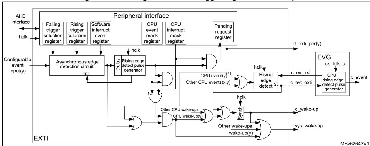
- 1. Only for the input events that support CPU rxeu generation c_event .
The software interrupt event register allows configurable events to be triggered by software, writing the corresponding register bit, whatever the edge selection setting.
The configurable event active trigger edge (or both edges) is selected and enabled in the rising/falling edge selection registers.
The CPU has its dedicated wake-up (interrupt) mask register and a dedicated event mask registers. When the event is enabled, it is generated to the CPU. All events for the CPU are ORed together into a single CPU event signal. The event pending registers (EXTI_RPR and EXTI_FPR) are not set for an unmasked CPU event.
The configurable events have unique interrupt pending request registers. The pending register is only set for an unmasked interrupt. Each configurable event provides a common interrupt to the CPU. The configurable event interrupts must be acknowledged by software in the EXTI_RPR and/or EXTI_FPR registers.
When a CPU wake-up (interrupt) or CPU event is enabled, the asynchronous edge detection circuit is reset by the clocked delay and rising edge detect pulse generator. This guarantees that the EXTI hclk clock is woken up before the asynchronous edge detection circuit is reset.
Note: A detected configurable event interrupt pending request can be cleared by the CPU with the correct access permission. The system is not able to enter into low-power modes as long as an interrupt pending request is active.
23.3.2 EXTI mux selection
The EXTI mux allows the selection of GPIOs as interrupts and wake-up. GPIOs are connected via 16 EXTI mux lines to the first 16 EXTI events as configurable event.
The selection of GPIO port as EXTI mux output is controlled in EXTI_EXTICRm.
Figure 103. EXTI mux GPIO selection
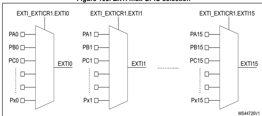
The diagram illustrates the EXTI mux selection for three specific interrupt lines: EXTI10, EXTI11, and EXTI15. Each line is controlled by a multiplexer (MUX) whose inputs are various GPIO pins from different ports (A, B, C, and X). For EXTI10, the inputs are PA0, PB0, PC0, ..., Px0. For EXTI11, the inputs are PA1, PB1, PC1, ..., Px1. For EXTI15, the inputs are PA15, PB15, PC15, ..., Px15. The outputs of these multiplexers are labeled EXTI10, EXTI11, ..., EXTI15. The control signals for these multiplexers are EXTI_EXTICR1.EXTI10, EXTI_EXTICR1.EXTI11, and EXTI_EXTICR1.EXTI15 respectively. A reference code MS44726V1 is shown in the bottom right corner.
The EXTI mux outputs are available as output signals from the EXTI to trigger other peripherals, whatever the masking in EXTI_IMR and EXTI_EMR registers.
23.4 EXTI functional behavior
The configurable events are enabled by enabling at least one of the trigger edges.
Once an event input is enabled, the CPU wake-up generation is conditioned by the CPU interrupt mask and CPU event mask.
Table 190. Masking functionality
| CPU interrupt enable (in EXTI_IMR.IMn) | CPU event enable (in EXTI_EMR.EMn) | Configurable event inputs (in EXTI_RPR.RPIFn and EXTI_FPR.FPIFn) | Exti(n) interrupt (1) | CPU event | CPU wake-up |
|---|---|---|---|---|---|
| 0 | 0 | No | Masked | Masked | Masked |
| 1 | No | Masked | Yes | Yes |
Table 190. Masking functionality (continued)
| CPU interrupt enable (in EXTI_IMR.IMn) | CPU event enable (in EXTI_EMR.EMn) | Configurable event inputs (in EXTI_RPR.RPIFn and EXTI_FPR.FPIFn) | Exti(n) interrupt (1) | CPU event | CPU wake-up |
|---|---|---|---|---|---|
| 1 | 0 | Status latched | Yes | Masked | Yes (2) |
| 1 | Status latched | Yes | Yes | Yes |
1. The single exti(n) interrupt goes to the CPU. If no interrupt is required for CPU(m), the exti(n) interrupt must be masked in the CPU NVIC.
2. Only if CPU interrupt is enabled in EXTI_IMR.IMn.
For configurable event inputs, when the enabled edges occur on the event input, an event request is generated. When the associated CPU interrupt is unmasked, the corresponding pending bits RPIFn in EXTI_RPR and/or FPIFn in EXTI_FPR is/are set: the CPU subsystem is woken up, and the CPU interrupt signal is activated. RPIFn and/or FPIFn must be cleared by the software writing them/it to one. This action clears the CPU interrupt.
For the configurable event inputs, an event request can be generated by software when writing a 1 in the software interrupt/event register EXTI_SWIER, allowing the generation of a rising edge on the event. The rising edge event pending bit is set in EXTI_RPR, whatever the setting in EXTI_RTSR.
23.5 EXTI event protection
The EXTI is able to protect event register bits from being modified by nonsecure and unprivileged accesses. The protection is individually activated per input event via the register bits in EXTI_SECCFGR and EXTI_PRIVCFGR. At EXTI level, the protection consists in preventing the following unauthorized write access:
- • Change the settings of the secure and/or privileged configurable events.
- • Change the masking of the secure and/or privileged input events.
- • Clear pending status of the secure and/or privileged input events.
Table 191. Register protection overview
| Register name | Access type | Protection (1)(2) |
|---|---|---|
| EXTI_RTSR | RW | Security and privilege can be bit-wise enabled in EXTI_SECCFGR and EXTI_PRIVCFGR. |
| EXTI_FTSR | RW | |
| EXTI_SWIER | RW | |
| EXTI_RPR | RW | |
| EXTI_FPR | RW | |
| EXTI_SECCFGR | RW | Always secure. Privilege can be bit-wise enabled in EXTI_PRIVCFGR. |
| EXTI_PRIVCFGR | RW | Always privilege. Security can be bit-wise enabled in EXTI_SECCFGR. |
| EXTI_EXTICRn | RW | Security and privilege can be bit-wise enabled in EXTI_SECCFGR and EXTI_PRIVCFGR. |
| EXTI_LOCKR | RW | Always secure |
| Register name | Access type | Protection (1)(2) |
|---|---|---|
| EXTI_IM | RW | Security and privilege can be bit-wise enabled in EXTI_SECCFGR and EXTI_PRIVCFGR. |
| EXTI_EMR | RW |
- 1. Security is enabled with the individual input event (EXTI_SECCFGR register).
- 2. Privilege is enabled with the individual input event (EXTI_PRIVCFGR register).
23.5.1 EXTI security protection
When security is enabled for an input event, the associated input event configuration and control bits can only be modified and read by a secure access. A nonsecure write access is discarded and a read returns 0.
When input events are nonsecure, the security is disabled. The associated input event configuration and control bits can be modified and read by a secure access and nonsecure access.
The security configuration in registers EXTI_SECCFGR can be globally locked after reset by LOCK in EXTI_LOCKR.
23.5.2 EXTI privilege protection
When privilege is enabled for an input event, the associated input event configuration and control bits can only be modified and read by a privileged access. An unprivileged write access is discarded, and a read access returns 0.
When input events are unprivileged, the privilege is disabled. The associated input event configuration and control bits can be modified and read by a privileged access and unprivileged access.
The privileged configuration in EXTI_PRIVCFGR registers can be globally locked after reset by LOCK in EXTI_LOCKR.
23.6 EXTI registers
The EXTI register map is divided in the following sections:
Table 192. EXTI register map sections
| Address offset | Description |
|---|---|
| 0x000 - 0x01C | General configurable event [22:0] configuration |
| 0x060 - 0x06C | EXTI IO port mux selection |
| 0x070 | EXTI protection lock configuration |
| 0x080 - 0x0BC | CPU input event configuration |
All registers can be accessed with word (32-bit), half-word (16-bit), and byte (8-bit) access.
23.6.1 EXTI rising trigger selection register (EXTI_RTSR1)
Address offset: 0x000
Reset value: 0x0000 0000
This register contains only bits for configurable events.
| 31 | 30 | 29 | 28 | 27 | 26 | 25 | 24 | 23 | 22 | 21 | 20 | 19 | 18 | 17 | 16 |
| Res | Res | Res | Res | Res | Res | RT25 | RT24 | RT23 | RT22 | RT21 | RT20 | RT19 | RT18 | RT17 | RT16 |
| rw | rw | rw | rw | rw | rw | rw | rw | rw | rw | ||||||
| 15 | 14 | 13 | 12 | 11 | 10 | 9 | 8 | 7 | 6 | 5 | 4 | 3 | 2 | 1 | 0 |
| RT15 | RT14 | RT13 | RT12 | RT11 | RT10 | RT9 | RT8 | RT7 | RT6 | RT5 | RT4 | RT3 | RT2 | RT1 | RT0 |
| rw | rw | rw | rw | rw | rw | rw | rw | rw | rw | rw | rw | rw | rw | rw | rw |
Bits 31:26 Reserved, must be kept at reset value.
Bits 25:0 RTx : Rising trigger event configuration bit of configurable event input x (1) (x = 25 to 0)
When EXTI_SECCFGR.SECx is disabled, RTx can be accessed with nonsecure and secure access.
When EXTI_SECCFGR.SECx is enabled, RTx can only be accessed with secure access. Nonsecure write to this bit x is discarded and nonsecure read returns 0.
When EXTI_PRIVCFGR.PRIVx is disabled, RTx can be accessed with unprivileged and privileged access.
When EXTI_PRIVCFGR.PRIVx is enabled, RTx can only be accessed with privileged access. Unprivileged write to this bit x is discarded, unprivileged read returns 0.
0: Rising trigger disabled (for event and interrupt) for input line
1: Rising trigger enabled (for event and interrupt) for input line
Note: RT25, RT24, and RT23 bits are only available on some devices in the STM32U5 Series. Refer to the EXTI line connections table for its availability. If not present, consider this bit as reserved and keep at reset value.
- 1. The configurable event inputs are edge triggered. No glitch must be generated on these inputs. If a rising edge on the configurable event input occurs during writing of the register, the associated pending bit is not set. Rising and falling edge triggers can be set for the same configurable event input. In this case, both edges generate a trigger.
23.6.2 EXTI falling trigger selection register (EXTI_FTSR1)
Address offset: 0x004
Reset value: 0x0000 0000
This register contains only bits for configurable events.
| 31 | 30 | 29 | 28 | 27 | 26 | 25 | 24 | 23 | 22 | 21 | 20 | 19 | 18 | 17 | 16 |
|---|---|---|---|---|---|---|---|---|---|---|---|---|---|---|---|
| Res. | Res. | Res. | Res. | Res. | Res. | FT25 | FT24 | FT23 | FT22 | FT21 | FT20 | FT19 | FT18 | FT17 | FT16 |
| rw | rw | rw | rw | rw | rw | rw | rw | rw | rw | ||||||
| 15 | 14 | 13 | 12 | 11 | 10 | 9 | 8 | 7 | 6 | 5 | 4 | 3 | 2 | 1 | 0 |
| FT15 | FT14 | FT13 | FT12 | FT11 | FT10 | FT9 | FT8 | FT7 | FT6 | FT5 | FT4 | FT3 | FT2 | FT1 | FT0 |
| rw | rw | rw | rw | rw | rw | rw | rw | rw | rw | rw | rw | rw | rw | rw | rw |
Bits 31:26 Reserved, must be kept at reset value.
Bits 25:0 FTx : Falling trigger event configuration bit of configurable event input x (1) (x = 25 to 0)
When EXTI_SECCFGR.SECx is disabled, FTx can be accessed with nonsecure and secure access.
When EXTI_SECCFGR.SECx is enabled, FTx can only be accessed with secure access. Nonsecure write to this FTx is discarded, nonsecure read returns 0.
When EXTI_PRIVCFGR.PRIVx is disabled, FTx can be accessed with unprivileged and privileged access.
When EXTI_PRIVCFGR.PRIVx is enabled, FTx can only be accessed with privileged access. Unprivileged write to this FTx is discarded, unprivileged read returns 0.
0: Falling trigger disabled (for event and interrupt) for input line
1: Falling trigger enabled (for event and interrupt) for input line.
Note: FT25, FT24, and FT23 bits are only available on some devices in the STM32U5 Series.
Refer to the EXTI line connections table for its availability. If not present, consider this bit as reserved and keep at reset value.
- 1. The configurable event inputs are edge triggered. No glitch must be generated on these inputs. If a falling edge on the configurable event input occurs during writing of the register, the associated pending bit is not set. Rising and falling edge triggers can be set for the same configurable event input. In this case, both edges generate a trigger.
23.6.3 EXTI software interrupt event register (EXTI_SWIER1)
Address offset: 0x008
Reset value: 0x0000 0000
This register contains only bits for configurable events.
| 31 | 30 | 29 | 28 | 27 | 26 | 25 | 24 | 23 | 22 | 21 | 20 | 19 | 18 | 17 | 16 |
|---|---|---|---|---|---|---|---|---|---|---|---|---|---|---|---|
| Res. | Res. | Res. | Res. | Res. | Res. | SWI25 | SWI24 | SWI23 | SWI22 | SWI21 | SWI20 | SWI19 | SWI18 | SWI17 | SWI16 |
| rw | rw | rw | rw | rw | rw | rw | rw | rw | rw | ||||||
| 15 | 14 | 13 | 12 | 11 | 10 | 9 | 8 | 7 | 6 | 5 | 4 | 3 | 2 | 1 | 0 |
| SWI15 | SWI14 | SWI13 | SWI12 | SWI11 | SWI10 | SWI9 | SWI8 | SWI7 | SWI6 | SWI5 | SWI4 | SWI3 | SWI2 | SWI1 | SWI0 |
| rw | rw | rw | rw | rw | rw | rw | rw | rw | rw | rw | rw | rw | rw | rw | rw |
Bits 31:26 Reserved, must be kept at reset value.
Bits 25:0 SWIx : Software interrupt on event x (x = 25 to 0)
When EXTI_SECCFGR.SECx is disabled, SWIx can be accessed with nonsecure and secure access.
When EXTI_SECCFGR.SECx is enabled, SWIx can only be accessed with secure access.
Nonsecure write to this SWI x is discarded, nonsecure read returns 0.
When EXTI_PRIVCFGR.PRIVx is disabled, SWIx can be accessed with unprivileged and privileged access.
When EXTI_PRIVCFGR.PRIVx is enabled, SWIx can only be accessed with privileged access. Unprivileged write to this SWIx is discarded, unprivileged read returns 0.
A software interrupt is generated independent from the setting in EXTI_RTSR and EXTI_FTSR. It always returns 0 when read.
0: Writing 0 has no effect.
1: Writing 1 triggers a rising edge event on event x. This bit is auto cleared by hardware.
Note: SW25, SW24, and SW23 bits are only available on some devices in the STM32U5 Series. Refer to the EXTI line connections table for its availability. If not present, consider this bit as reserved and keep at reset value.
23.6.4 EXTI rising edge pending register (EXTI_RPR1)
Address offset: 0x00C
Reset value: 0x0000 0000
This register contains only bits for configurable events.
| 31 | 30 | 29 | 28 | 27 | 26 | 25 | 24 | 23 | 22 | 21 | 20 | 19 | 18 | 17 | 16 |
|---|---|---|---|---|---|---|---|---|---|---|---|---|---|---|---|
| Res. | Res. | Res. | Res. | Res. | Res. | RPIF25 | RPIF24 | RPIF23 | RPIF22 | RPIF21 | RPIF20 | RPIF19 | RPIF18 | RPIF17 | RPIF16 |
| rc_w1 | rc_w1 | rc_w1 | rc_w1 | rc_w1 | rc_w1 | rc_w1 | rc_w1 | rc_w1 | rc_w1 | ||||||
| 15 | 14 | 13 | 12 | 11 | 10 | 9 | 8 | 7 | 6 | 5 | 4 | 3 | 2 | 1 | 0 |
| RPIF15 | RPIF14 | RPIF13 | RPIF12 | RPIF11 | RPIF10 | RPIF9 | RPIF8 | RPIF7 | RPIF6 | RPIF5 | RPIF4 | RPIF3 | RPIF2 | RPIF1 | RPIF0 |
| rc_w1 | rc_w1 | rc_w1 | rc_w1 | rc_w1 | rc_w1 | rc_w1 | rc_w1 | rc_w1 | rc_w1 | rc_w1 | rc_w1 | rc_w1 | rc_w1 | rc_w1 | rc_w1 |
Bits 31:26 Reserved, must be kept at reset value.
Bits 25:0 RPIFx : configurable event inputs x rising edge pending bit (x = 25 to 0)
When EXTI_SECCFGR.SECx is disabled, RPIFx can be accessed with nonsecure and secure access.
When EXTI_SECCFGR.SECx is enabled, RPIFx can only be accessed with secure access.
Nonsecure write to this RPIFx is discarded, nonsecure read returns 0.
When EXTI_PRIVCFGR.PRIVx is disabled, RPIFx can be accessed with unprivileged and privileged access.
When EXTI_PRIVCFGR.PRIVx is enabled, RPIFx can only be accessed with privileged access. Unprivileged write to this RPIFx is discarded, unprivileged read returns 0.
0: No rising edge trigger request occurred
1: Rising edge trigger request occurred
This bit is set when the rising edge event or an EXTI_SWIER software trigger arrives on the configurable event line. This bit is cleared by writing 1 to it.
Note: RPIF25, RPIF24, and RPIF23 bits are only available on some devices in the STM32U5 Series. Refer to the EXTI line connections table for its availability. If not present, consider this bit as reserved and keep at reset value.
23.6.5 EXTI falling edge pending register (EXTI_FPR1)
Address offset: 0x010
Reset value: 0x0000 0000
This register contains only bits for configurable events.
| 31 | 30 | 29 | 28 | 27 | 26 | 25 | 24 | 23 | 22 | 21 | 20 | 19 | 18 | 17 | 16 |
|---|---|---|---|---|---|---|---|---|---|---|---|---|---|---|---|
| Res. | Res. | Res. | Res. | Res. | Res. | FPIF25 | FPIF24 | FPIF23 | FPIF22 | FPIF21 | FPIF20 | FPIF19 | FPIF18 | FPIF17 | FPIF16 |
| rc_w1 | rc_w1 | rc_w1 | rc_w1 | rc_w1 | rc_w1 | rc_w1 | rc_w1 | rc_w1 | rc_w1 | ||||||
| 15 | 14 | 13 | 12 | 11 | 10 | 9 | 8 | 7 | 6 | 5 | 4 | 3 | 2 | 1 | 0 |
| FPIF15 | FPIF14 | FPIF13 | FPIF12 | FPIF11 | FPIF10 | FPIF9 | FPIF8 | FPIF7 | FPIF6 | FPIF5 | FPIF4 | FPIF3 | FPIF2 | FPIF1 | FPIF0 |
| rc_w1 | rc_w1 | rc_w1 | rc_w1 | rc_w1 | rc_w1 | rc_w1 | rc_w1 | rc_w1 | rc_w1 | rc_w1 | rc_w1 | rc_w1 | rc_w1 | rc_w1 | rc_w1 |
Bits 31:26 Reserved, must be kept at reset value.
Bits 25:0 FPIFx : configurable event inputs x falling edge pending bit (x = 25 to 0)
- When EXTI_SECCFGR.SECx is disabled, FPIFx can be accessed with nonsecure and secure access.
- When EXTI_SECCFGR.SECx is enabled, FPIFx can only be accessed with secure access. Nonsecure write to this FPIFx is discarded, nonsecure read returns 0.
- When EXTI_PRIVCFGR.PRIVx is disabled, FPIFx can be accessed with unprivileged and privileged access.
- When EXTI_PRIVCFGR.PRIVx is enabled, FPIFx can only be accessed with privileged access. Unprivileged write to this FPIFx is discarded, unprivileged read returns 0.
- 0: No falling edge trigger request occurred
- 1: Falling edge trigger request occurred
This bit is set when the falling edge event arrives on the configurable event line. This bit is cleared by writing 1 to it.
Note: FPIF25, FPIF24, and FPIF23 bits are only available on some devices in the STM32U5 Series. Refer to the EXTI line connections table for its availability. If not present, consider this bit as reserved and keep at reset value.
23.6.6 EXTI security configuration register (EXTI_SECCFGR1)
Address offset: 0x014
Reset value: 0x0000 0000
This register provides write access security, a nonsecure write access is ignored and causes the generation of an illegal access event. A nonsecure read returns the register data. This register contains only bits for security capable input events..
| 31 | 30 | 29 | 28 | 27 | 26 | 25 | 24 | 23 | 22 | 21 | 20 | 19 | 18 | 17 | 16 |
|---|---|---|---|---|---|---|---|---|---|---|---|---|---|---|---|
| Res. | Res. | Res. | Res. | Res. | Res. | SEC25 | SEC24 | SEC23 | SEC22 | SEC21 | SEC20 | SEC19 | SEC18 | SEC17 | SEC16 |
| rw | rw | rw | rw | rw | rw | rw | rw | rw | rw | ||||||
| 15 | 14 | 13 | 12 | 11 | 10 | 9 | 8 | 7 | 6 | 5 | 4 | 3 | 2 | 1 | 0 |
| SEC15 | SEC14 | SEC13 | SEC12 | SEC11 | SEC10 | SEC9 | SEC8 | SEC7 | SEC6 | SEC5 | SEC4 | SEC3 | SEC2 | SEC1 | SEC0 |
| rw | rw | rw | rw | rw | rw | rw | rw | rw | rw | rw | rw | rw | rw | rw | rw |
Bits 31:26 Reserved, must be kept at reset value.
Bits 25:0 SECx : Security enable on event input x (x = 25 to 0)
When EXTI_PRIVCFG.PRIVx is disabled, SECx can be accessed with privileged and unprivileged access.
When EXTI_PRIVCFG.PRIVx is enabled, SECx can only be written with privileged access.
Unprivileged write to this SECx is discarded.
0: Event security disabled (nonsecure)
1: Event security enabled (secure)
Note: SEC25, SEC24, and SEC23 bits are only available on some devices in the STM32U5 Series. Refer to the EXTI line connections table for its availability. If not present, consider this bit as reserved and keep at reset value.
23.6.7 EXTI privilege configuration register (EXTI_PRIVCFG1)
Address offset: 0x018
Reset value: 0x0000 0000
This register provides privileged write access protection. An unprivileged read returns the register data. This register contains only bits for security capable input events.
| 31 | 30 | 29 | 28 | 27 | 26 | 25 | 24 | 23 | 22 | 21 | 20 | 19 | 18 | 17 | 16 |
|---|---|---|---|---|---|---|---|---|---|---|---|---|---|---|---|
| Res. | Res. | Res. | Res. | Res. | Res. | PRIV25 | PRIV24 | PRIV23 | PRIV22 | PRIV21 | PRIV20 | PRIV19 | PRIV18 | PRIV17 | PRIV16 |
| rw | rw | rw | rw | rw | rw | rw | rw | rw | rw | ||||||
| 15 | 14 | 13 | 12 | 11 | 10 | 9 | 8 | 7 | 6 | 5 | 4 | 3 | 2 | 1 | 0 |
| PRIV15 | PRIV14 | PRIV13 | PRIV12 | PRIV11 | PRIV10 | PRIV9 | PRIV8 | PRIV7 | PRIV6 | PRIV5 | PRIV4 | PRIV3 | PRIV2 | PRIV1 | PRIV0 |
| rw | rw | rw | rw | rw | rw | rw | rw | rw | rw | rw | rw | rw | rw | rw | rw |
Bits 31:26 Reserved, must be kept at reset value.
Bits 25:0 PRIVx : Security enable on event input x (x = 25 to 0)
When EXTI_SECCFG.SECx is disabled, PRIVx can be accessed with secure and nonsecure access.
When EXTI_SECCFG.SECx is enabled, PRIVx can only be written with secure access.
Nonsecure write to this PRIVx is discarded.
0: Event privilege disabled (unprivileged)
1: Event privilege enabled (privileged)
Note: PRIV25, PRIV24, and PRIV23 bits are only available on some devices in the STM32U5 Series. Refer to the EXTI line connections table for its availability. If not present, consider this bit as reserved and keep at reset value.
23.6.8 EXTI external interrupt selection register (EXTI_EXTICRm)
Address offset: 0x060 + 0x4 * (m - 1) (m = 1 to 4)
Reset value: 0x0000 0000
| 31 | 30 | 29 | 28 | 27 | 26 | 25 | 24 | 23 | 22 | 21 | 20 | 19 | 18 | 17 | 16 |
|---|---|---|---|---|---|---|---|---|---|---|---|---|---|---|---|
| EXTI{4*(m-1)+3}[7:0] | EXTI{4*(m-1)+2}[7:0] | ||||||||||||||
| rw | rw | rw | rw | rw | rw | rw | rw | rw | rw | rw | rw | rw | rw | rw | rw |
| 15 | 14 | 13 | 12 | 11 | 10 | 9 | 8 | 7 | 6 | 5 | 4 | 3 | 2 | 1 | 0 |
| EXTI{4*(m-1)+1}[7:0] | EXTI{4*(m-1)}[7:0] | ||||||||||||||
| rw | rw | rw | rw | rw | rw | rw | rw | rw | rw | rw | rw | rw | rw | rw | rw |
Bits 31:24 EXTI{4*(m-1)+3}[7:0]: EXTI{4*(m-1)+3} GPIO port selection
These bits are written by software to select the source input for EXTI{4*(m-1)+3} external interrupt.
When EXTI_SECCFGR.SEC{4*(m-1)+3} is disabled, this field can be accessed with nonsecure and secure access.
When EXTI_SECCFGR.SEC{4*(m-1)+3} is enabled, this field can only be accessed with secure access. Nonsecure write is discarded, and nonsecure read returns 0.
When EXTI_PRIVCFGR.PRIV{4*(m-1)+3} is disabled, this field can be accessed with privileged and unprivileged access.
When EXTI_PRIVCFGR.PRIV{4*(m-1)+3} is enabled, this field can only be accessed with privileged access. Unprivileged write to this bit is discarded.
0x00: PA{4*(m-1)+3} pin
0x01: PB{4*(m-1)+3} pin
0x02: PC{4*(m-1)+3} pin
0x03: PD{4*(m-1)+3} pin
0x04: PE{4*(m-1)+3} pin
0x05: PF{4*(m-1)+3} pin
0x06: PG{4*(m-1)+3} pin
0x07: PH{4*(m-1)+3} pin
0x08: PI{4*(m-1)+3} pin
0x09: PJ{4*(m-1)+3} pin
Others: reserved
Bits 23:16 EXTI{4*(m-1)+2}[7:0]: EXTI{4*(m-1)+2} GPIO port selectionThese bits are written by software to select the source input for the EXTI{4*(m-1)+2} external interrupt.
When EXTI_SECCFGR.SEC{4*(m-1)+2} is disabled, this field can be accessed with nonsecure and secure access.
When EXTI_SECCFGR.SEC{4*(m-1)+2} is enabled, this field can only be accessed with secure access. Nonsecure write is discarded, and nonsecure read returns 0.
When EXTI_PRIVCFGR.PRIV{4*(m-1)+2} is disabled, this field can be accessed with privileged and unprivileged access.
When EXTI_PRIVCFGR.PRIV{4*(m-1)+2} is enabled, this field can only be accessed with privileged access. Unprivileged write to this bit is discarded.
0x00: PA[{4*(m-1)+2}] pin
0x01: PB[{4*(m-1)+2}] pin
0x02: PC[{4*(m-1)+2}] pin
0x03: PD[{4*(m-1)+2}] pin
0x04: PE[{4*(m-1)+2}] pin
0x05: PF[{4*(m-1)+2}] pin
0x06: PG[{4*(m-1)+2}] pin
0x07: PH[{4*(m-1)+2}] pin
0x08: PI[{4*(m-1)+2}] pin
0x09: PJ[{4*(m-1)+2}] pin
Others: reserved
Bits 15:8 EXTI{4*(m-1)+1}[7:0]: EXTI{4*(m-1)+1} GPIO port selectionThese bits are written by software to select the source input for EXTI{4*(m-1)+1} external interrupt.
When EXTI_SECCFGR.SEC{4*(m-1)+1} is disabled, this field can be accessed with nonsecure and secure access.
When EXTI_SECCFGR.SEC{4*(m-1)+1} is enabled, this field can only be accessed with secure access. Nonsecure write is discarded and nonsecure read returns 0.
When EXTI_PRIVCFGR.PRIV{4*(m-1)+1} is disabled, this field can be accessed with privileged and unprivileged access.
When EXTI_PRIVCFGR.PRIV{4*(m-1)+1} is enabled, this field can only be accessed with privileged access. Unprivileged write to this bit is discarded.
0x00: PA[{4*(m-1)+1}] pin
0x01: PB[{4*(m-1)+1}] pin
0x02: PC[{4*(m-1)+1}] pin
0x03: PD[{4*(m-1)+1}] pin
0x04: PE[{4*(m-1)+1}] pin
0x05: PF[{4*(m-1)+1}] pin
0x06: PG[{4*(m-1)+1}] pin
0x07: PH[{4*(m-1)+1}] pin
0x08: PI[{4*(m-1)+1}] pin
0x09: PJ[{4*(m-1)+1}] pin
Others: reserved
Bits 7:0 EXTI{4*(m-1)}[7:0] : EXTI{4*(m-1)} GPIO port selection
These bits are written by software to select the source input for EXTI{4*(m-1)} external interrupt.
When EXTI_SECCFGR.SEC{4*(m-1)} is disabled, this field can be accessed with nonsecure and secure access.
When EXTI_SECCFGR.SEC{4*(m-1)} is enabled, this field can only be accessed with secure access. Nonsecure write is discarded and nonsecure read returns 0.
When EXTI_PRIVCFGR.PRIV{4*(m-1)} is disabled, this field can be accessed with privileged and unprivileged access.
When EXTI_PRIVCFGR.PRIV{4*(m-1)} is enabled, this field can only be accessed with privilege access. Unprivileged write to this bit is discarded.
0x00: PA{4*(m-1)} pin
0x01: PB{4*(m-1)} pin
0x02: PC{4*(m-1)} pin
0x03: PD{4*(m-1)} pin
0x04: PE{4*(m-1)} pin
0x05: PF{4*(m-1)} pin
0x06: PG{4*(m-1)} pin
0x07: PH{4*(m-1)} pin
0x08: PI{4*(m-1)} pin
0x09: PJ{4*(m-1)} pin
Others: reserved
23.6.9 EXTI lock register (EXTI_LOCKR)
Address offset: 0x070
Reset value: 0x0000 0000
This register provides write access security: a nonsecure write access is ignored, a read access returns zero data, and both generates an illegal access event.
| 31 | 30 | 29 | 28 | 27 | 26 | 25 | 24 | 23 | 22 | 21 | 20 | 19 | 18 | 17 | 16 |
|---|---|---|---|---|---|---|---|---|---|---|---|---|---|---|---|
| Res. | Res. | Res. | Res. | Res. | Res. | Res. | Res. | Res. | Res. | Res. | Res. | Res. | Res. | Res. | Res. |
| 15 | 14 | 13 | 12 | 11 | 10 | 9 | 8 | 7 | 6 | 5 | 4 | 3 | 2 | 1 | 0 |
| Res | Res | Res | Res | Res | Res | Res | Res | Res | Res | Res | Res | Res | Res | Res | LOCK |
| rs |
Bits 31:1 Reserved, must be kept at reset value.
Bit 0 LOCK : Global security and privilege configuration registers (EXTI_SECCFGR and EXTI_PRIVCFGR) lock
This bit is written once after reset.
0: Security and privilege configuration open, can be modified.
1: Security and privilege configuration locked, can no longer be modified.
23.6.10 EXTI CPU wake-up with interrupt mask register (EXTI_IMR1)
Address offset: 0x080
Reset value: 0x0000 0000
This register contains bits for configurable events.
| 31 | 30 | 29 | 28 | 27 | 26 | 25 | 24 | 23 | 22 | 21 | 20 | 19 | 18 | 17 | 16 |
|---|---|---|---|---|---|---|---|---|---|---|---|---|---|---|---|
| Res. | Res. | Res. | Res. | Res. | Res. | IM25 | IM24 | IM23 | IM22 | IM21 | IM20 | IM19 | IM18 | IM17 | IM16 |
| 15 | 14 | 13 | 12 | 11 | 10 | 9 | 8 | 7 | 6 | 5 | 4 | 3 | 2 | 1 | 0 |
| IM15 | IM14 | IM13 | IM12 | IM11 | IM10 | IM9 | IM8 | IM7 | IM6 | IM5 | IM4 | IM3 | IM2 | IM1 | IM0 |
| rw | rw | rw | rw | rw | rw | rw | rw | rw | rw | rw | rw | rw | rw | rw | rw |
Bits 31:26 Reserved, must be kept at reset value.
Bits 25:0 IMx : CPU wake-up with interrupt mask on event input x (1) (x = 25 to 0)
When EXTI_SECCFGR.SECx is disabled, IMx can be accessed with nonsecure and secure access.
When EXTI_SECCFGR.SECx is enabled, IMx can only be accessed with secure access.
Nonsecure write to this bit is discarded and nonsecure read returns 0.
When EXTI_PRIVCFGR.PRIVx is disabled, IMx can be accessed with privileged and unprivileged access.
When EXTI_PRIVCFGR.PRIVx is enabled, IMx can only be accessed with privileged access. Unprivileged write to this bit is discarded.
0: Wake-up with interrupt request from input event x is masked.
1: Wake-up with interrupt request from input event x is unmasked.
Note: IM25, IM24, and IM23 bits are only available on some devices in the STM32U5 Series.
Refer to the EXTI line connections table for its availability. If not present, consider this bit as reserved and keep at reset value.
- 1. The reset value for configurable event inputs is set to 0 in order to disable the interrupt by default.
23.6.11 EXTI CPU wake-up with event mask register (EXTI_EMR1)
Address offset: 0x084
Reset value: 0x0000 0000
| 31 | 30 | 29 | 28 | 27 | 26 | 25 | 24 | 23 | 22 | 21 | 20 | 19 | 18 | 17 | 16 |
|---|---|---|---|---|---|---|---|---|---|---|---|---|---|---|---|
| Res. | Res. | Res. | Res. | Res. | Res. | EM25 | EM24 | EM23 | EM22 | EM21 | EM20 | EM19 | EM18 | EM17 | EM16 |
| 15 | 14 | 13 | 12 | 11 | 10 | 9 | 8 | 7 | 6 | 5 | 4 | 3 | 2 | 1 | 0 |
| EM15 | EM14 | EM13 | EM12 | EM11 | EM10 | EM9 | EM8 | EM7 | EM6 | EM5 | EM4 | EM3 | EM2 | EM1 | EM0 |
| rw | rw | rw | rw | rw | rw | rw | rw | rw | rw | rw | rw | rw | rw | rw | rw |
Bits 31:26 Reserved, must be kept at reset value.
Bits 25:0 EMx : CPU wake-up with event generation mask on event input x (x = 25 to 0)
When EXTI_SECCFGR.SECx is disabled, EMx can be accessed with nonsecure and secure access.
When EXTI_SECCFGR.SECx is enabled, EMx can only be accessed with secure access.
Nonsecure write to this bit x is discarded and nonsecure read returns 0.
When EXTI_PRIVCFGR.PRIVx is disabled, EMx can be accessed with privileged and unprivileged access.
When EXTI_PRIVCFGR.PRIVx is enabled, EMx can only be accessed with privileged access. Unprivileged write to this bit is discarded.
0: Wake-up with event generation from line x is masked.
1: Wake-up with event generation from line x is unmasked.
Note: EM25, EM24, and EM23 bits are only available on some devices in the STM32U5 Series. Refer to the EXTI line connections table for its availability. If not present, consider this bit as reserved and keep at reset value.
23.6.12 EXTI register map
Table 193. EXTI register map and reset values
| Offset | Register name | 31 | 30 | 29 | 28 | 27 | 26 | 25 | 24 | 23 | 22 | 21 | 20 | 19 | 18 | 17 | 16 | 15 | 14 | 13 | 12 | 11 | 10 | 9 | 8 | 7 | 6 | 5 | 4 | 3 | 2 | 1 | 0 |
|---|---|---|---|---|---|---|---|---|---|---|---|---|---|---|---|---|---|---|---|---|---|---|---|---|---|---|---|---|---|---|---|---|---|
| 0x000 | EXTI_RTSR1 | Res. | Res. | Res. | Res. | Res. | Res. | RT25 | RT24 | RT23 | RT22 | RT21 | RT20 | RT19 | RT18 | RT17 | RT16 | RT15 | RT14 | RT13 | RT12 | RT11 | RT10 | RT9 | RT8 | RT7 | RT6 | RT5 | RT4 | RT3 | RT2 | RT1 | RT0 |
| Reset value | 0 | 0 | 0 | 0 | 0 | 0 | 0 | 0 | 0 | 0 | 0 | 0 | 0 | 0 | 0 | 0 | 0 | 0 | 0 | 0 | 0 | 0 | 0 | 0 | 0 | 0 | |||||||
| 0x004 | EXTI_FTSR1 | Res. | Res. | Res. | Res. | Res. | Res. | FT25 | FT24 | FT23 | FT22 | FT21 | FT20 | FT19 | FT18 | FT17 | FT16 | FT15 | FT14 | FT13 | FT12 | FT11 | FT10 | FT9 | FT8 | FT7 | FT6 | FT5 | FT4 | FT3 | FT2 | FT1 | FT0 |
| Reset value | 0 | 0 | 0 | 0 | 0 | 0 | 0 | 0 | 0 | 0 | 0 | 0 | 0 | 0 | 0 | 0 | 0 | 0 | 0 | 0 | 0 | 0 | 0 | 0 | 0 | 0 | |||||||
| 0x008 | EXTI_SWIER1 | Res. | Res. | Res. | Res. | Res. | Res. | SWI25 | SWI24 | SWI23 | SWI22 | SWI21 | SWI20 | SWI19 | SWI18 | SWI17 | SWI16 | SWI15 | SWI14 | SWI13 | SWI12 | SWI11 | SWI10 | SWI9 | SWI8 | SWI7 | SWI6 | SWI5 | SWI4 | SWI3 | SWI2 | SWI1 | SWI0 |
| Reset value | 0 | 0 | 0 | 0 | 0 | 0 | 0 | 0 | 0 | 0 | 0 | 0 | 0 | 0 | 0 | 0 | 0 | 0 | 0 | 0 | 0 | 0 | 0 | 0 | 0 | 0 | |||||||
| 0x00C | EXTI_RPR1 | Res. | Res. | Res. | Res. | Res. | Res. | RPIF25 | RPIF24 | RPIF23 | RPIF22 | RPIF21 | RPIF20 | RPIF19 | RPIF18 | RPIF17 | RPIF16 | RPIF15 | RPIF14 | RPIF13 | RPIF12 | RPIF11 | RPIF10 | RPIF9 | RPIF8 | RPIF7 | RPIF6 | RPIF5 | RPIF4 | RPIF3 | RPIF2 | RPIF1 | RPIF0 |
| Reset value | 0 | 0 | 0 | 0 | 0 | 0 | 0 | 0 | 0 | 0 | 0 | 0 | 0 | 0 | 0 | 0 | 0 | 0 | 0 | 0 | 0 | 0 | 0 | 0 | 0 | 0 | |||||||
| 0x010 | EXTI_FPR1 | Res. | Res. | Res. | Res. | Res. | Res. | FPIF25 | FPIF24 | FPIF23 | FPIF22 | FPIF21 | FPIF20 | FPIF19 | FPIF18 | FPIF17 | FPIF16 | FPIF15 | FPIF14 | FPIF13 | FPIF12 | FPIF11 | FPIF10 | FPIF9 | FPIF8 | FPIF7 | FPIF6 | FPIF5 | FPIF4 | FPIF3 | FPIF2 | FPIF1 | FPIF0 |
| Reset value | 0 | 0 | 0 | 0 | 0 | 0 | 0 | 0 | 0 | 0 | 0 | 0 | 0 | 0 | 0 | 0 | 0 | 0 | 0 | 0 | 0 | 0 | 0 | 0 | 0 | 0 | |||||||
| 0x014 | EXTI_SECCFGR1 | Res. | Res. | Res. | Res. | Res. | Res. | SEC25 | SEC24 | SEC23 | SEC22 | SEC21 | SEC20 | SEC19 | SEC18 | SEC17 | SEC16 | SEC15 | SEC14 | SEC13 | SEC12 | SEC11 | SEC10 | SEC9 | SEC8 | SEC7 | SEC6 | SEC5 | SEC4 | SEC3 | SEC2 | SEC1 | SEC0 |
| Reset value | 0 | 0 | 0 | 0 | 0 | 0 | 0 | 0 | 0 | 0 | 0 | 0 | 0 | 0 | 0 | 0 | 0 | 0 | 0 | 0 | 0 | 0 | 0 | 0 | 0 | 0 | |||||||
| 0x018 | EXTI_PRIVCFGR1 | Res. | Res. | Res. | Res. | Res. | Res. | PRIV25 | PRIV24 | PRIV23 | PRIV22 | PRIV21 | PRIV20 | PRIV19 | PRIV18 | PRIV17 | PRIV16 | PRIV15 | PRIV14 | PRIV13 | PRIV12 | PRIV11 | PRIV10 | PRIV9 | PRIV8 | PRIV7 | PRIV6 | PRIV5 | PRIV4 | PRIV3 | PRIV2 | PRIV1 | PRIV0 |
| Reset value | 0 | 0 | 0 | 0 | 0 | 0 | 0 | 0 | 0 | 0 | 0 | 0 | 0 | 0 | 0 | 0 | 0 | 0 | 0 | 0 | 0 | 0 | 0 | 0 | 0 | 0 | |||||||
| 0x020-0x05C | Reserved | Reserved | |||||||||||||||||||||||||||||||
| 0x060 | EXTI_EXTICR1 | EXTI3[7:0] | EXTI2[7:0] | EXTI1[7:0] | EXTI0[7:0] | ||||||||||||||||||||||||||||
| Reset value | 0 | 0 | 0 | 0 | 0 | 0 | 0 | 0 | 0 | 0 | 0 | 0 | 0 | 0 | 0 | 0 | 0 | 0 | 0 | 0 | 0 | 0 | 0 | 0 | 0 | 0 | 0 | 0 | 0 | 0 | 0 | 0 | |
| 0x064 | EXTI_EXTICR2 | EXTI7[7:0] | EXTI6[7:0] | EXTI5[7:0] | EXTI4[7:0] | ||||||||||||||||||||||||||||
| Reset value | 0 | 0 | 0 | 0 | 0 | 0 | 0 | 0 | 0 | 0 | 0 | 0 | 0 | 0 | 0 | 0 | 0 | 0 | 0 | 0 | 0 | 0 | 0 | 0 | 0 | 0 | 0 | 0 | 0 | 0 | 0 | 0 | |
Table 193. EXTI register map and reset values (continued)
| Offset | Register name | 31 | 30 | 29 | 28 | 27 | 26 | 25 | 24 | 23 | 22 | 21 | 20 | 19 | 18 | 17 | 16 | 15 | 14 | 13 | 12 | 11 | 10 | 9 | 8 | 7 | 6 | 5 | 4 | 3 | 2 | 1 | 0 | ||
|---|---|---|---|---|---|---|---|---|---|---|---|---|---|---|---|---|---|---|---|---|---|---|---|---|---|---|---|---|---|---|---|---|---|---|---|
| 0x068 | EXTI_EXTICR3 | EXTI11[7:0] | EXTI10[7:0] | EXTI9[7:0] | EXTI8[7:0] | ||||||||||||||||||||||||||||||
| Reset value | 0 | 0 | 0 | 0 | 0 | 0 | 0 | 0 | 0 | 0 | 0 | 0 | 0 | 0 | 0 | 0 | 0 | 0 | 0 | 0 | 0 | 0 | 0 | 0 | 0 | 0 | 0 | 0 | 0 | 0 | 0 | 0 | |||
| 0x06C | EXTI_EXTICR4 | EXTI15[7:0] | EXTI14[7:0] | EXTI13[7:0] | EXTI2[7:0] | ||||||||||||||||||||||||||||||
| Reset value | 0 | 0 | 0 | 0 | 0 | 0 | 0 | 0 | 0 | 0 | 0 | 0 | 0 | 0 | 0 | 0 | 0 | 0 | 0 | 0 | 0 | 0 | 0 | 0 | 0 | 0 | 0 | 0 | 0 | 0 | 0 | 0 | |||
| 0x070 | EXTI_LOCKR | Res. | Res. | Res. | Res. | Res. | Res. | Res. | Res. | Res. | Res. | Res. | Res. | Res. | Res. | Res. | Res. | Res. | Res. | Res. | Res. | Res. | Res. | Res. | Res. | Res. | Res. | Res. | Res. | Res. | Res. | Res. | LOCK | ||
| Reset value | 0 | ||||||||||||||||||||||||||||||||||
| 0x074- 0x07C | Reserved | Reserved | |||||||||||||||||||||||||||||||||
| 0x080 | EXTI_IMR1 | Res. | Res. | Res. | Res. | Res. | Res. | IM25 | IM24 | IM23 | IM22 | IM21 | IM20 | IM19 | IM18 | IM17 | IM16 | IM15 | IM14 | IM13 | IM12 | IM11 | IM10 | IM9 | IM8 | IM7 | IM6 | IM5 | IM4 | IM3 | IM2 | IM1 | IM0 | ||
| Reset value | 0 | 0 | 0 | 0 | 0 | 0 | 0 | 0 | 0 | 0 | 0 | 0 | 0 | 0 | 0 | 0 | 0 | 0 | 0 | 0 | 0 | 0 | 0 | 0 | 0 | 0 | |||||||||
| 0x084 | EXTI_EMR1 | Res. | Res. | Res. | Res. | Res. | Res. | EM25 | EM24 | EM23 | EM22 | EM21 | EM20 | EM19 | EM18 | EM17 | EM16 | EM15 | EM14 | EM13 | EM12 | EM11 | EM10 | EM9 | EM8 | EM7 | EM6 | EM5 | EM4 | EM3 | EM2 | EM1 | EM0 | ||
| Reset value | 0 | 0 | 0 | 0 | 0 | 0 | 0 | 0 | 0 | 0 | 0 | 0 | 0 | 0 | 0 | 0 | 0 | 0 | 0 | 0 | 0 | 0 | 0 | 0 | 0 | 0 | |||||||||
Refer to Section 2.3 for the register boundary addresses.