15. System configuration controller (SYSCFG)
15.1 SYSCFG main features
The STM32U5 series devices feature a set of configuration registers. The main purposes of the system configuration controller are the following:
- • Managing robustness feature
- • Configuring FPU interrupts
- • Enabling/disabling the FMP high-drive mode of some I/Os and voltage booster for I/Os analog switches
- • Managing the I/O compensation cell
- • Configuring register security access
- • Configuring the OTG_HS PHY (only for STM32U59x/5Ax/5Fx/5Gx)
- • Adjust the HSPI supply capacitance (only for STM32U59x/5Ax/5Fx/5Gx)
- • Disable internal SRAMs cacheability by DCACHE2 (only for STM32U59x/5Ax/5Fx/5Gx)
15.2 SYSCFG functional description
15.2.1 I/O compensation cell management
The I/O compensation cell generates an 8-bit value for the I/O buffer (4 bits for N-MOS and 4 bits for P-MOS), which depends on PVT operating conditions (process, voltage, temperature). These bits are used to control the current slew-rate and output impedance in the I/O buffer. Three compensation cells are embedded, one for the I/Os supplied by \( V_{DD} \) , one for the I/Os supplied by \( V_{DDIO2} \) , and one dedicated to GPIOs with HSPI alternate functions (AF) capabilities.
By default, the compensation cells are disabled, and a fixed code is applied to all the I/Os. The HSI is used by the compensation cells and must be enabled before enabling the compensation cells in SYSCFG_CCCSR.
When enabled, the compensation cell tracks the PVT, and the 8-bit code PCVx and NCVx ( \( x = 1 \) for I/Os supplied by \( V_{DD} \) except the HSPI AF capabilities, \( x = 2 \) for I/Os supplied by \( V_{DDIO2} \) and \( x = 3 \) for I/Os with HSPI AF capabilities supplied by \( V_{DD} \) ) are available in SYSCFG_CCVR once the RDYx is set. If the CSx bit is cleared, the I/Ox receives the code from SYSCFG_CCVR, resulting from the compensation cell.
To optimize the trimming, the code can be adjusted through SYSCFG_CCCR. Three sets of bits are available: PCC1/NCC1 and PCC3/NCC3 for the \( V_{DD} \) power rail, and PCC2/NCC2 for the \( V_{DDIO2} \) power rail. They can be selected independently through CS1, CS2, and CS3 bits in SYSCFG_CCCSR (see Figure 50 ).
To reduce the power consumption, it is recommended to copy the code from SYSCFG_CCVR to SYSCFG_CCCR. After the result is ready, set the CSx bit and disable the compensation cell.
Note: The compensation cell can be used only when \( 1.6\text{ V} \leq V_{DDIOx} \leq 3.6\text{ V} \) .
Figure 50. I/O compensation cell block diagram
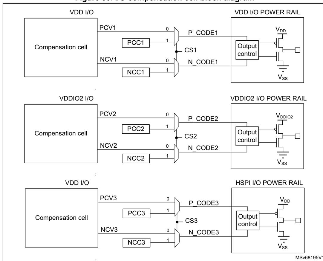
The diagram illustrates the internal structure of I/O compensation cells for three different I/O types: VDD I/O, VDDIO2 I/O, and HSPI I/O. Each cell contains a 'Compensation cell' block that provides two signals: PCV (0) and NCV (1). These signals are processed by 'PCC' and 'NCC' blocks to generate 'P_CODE' and 'N_CODE' signals. These signals are then passed to an 'Output control' block, which is connected to a power rail (VDD I/O POWER RAIL, VDDIO2 I/O POWER RAIL, or HSPI I/O POWER RAIL). The power rail is connected to a circuit consisting of a PMOS transistor connected to V DD and an NMOS transistor connected to V SS . The Output control block is connected to the gates of these transistors. The diagram is labeled with 'MSv68195V1' in the bottom right corner.
15.2.2 SYSCFG TrustZone security and privilege
SYSCFG TrustZone security
When the TrustZone security is activated, the SYSCFG is able to secure registers from being modified by nonsecure accesses.
The TrustZone security is activated by the TZEN option bit in the FLASH_OPTR register.
A nonsecure read/write access to a secured register is RAZ/WI and generates an illegal access event. An illegal access interrupt is generated if the SYSCFG illegal access event is enabled in the GTZC.
Privileged/unprivileged mode
The SYSCFG registers can be read and written by privileged and unprivileged accesses except the SYSCFG registers for CPU configuration: SYSCFG_CSLCKR, SYSCFG_FPUIMR and SYSCFG_CNSLCKR registers, and the FPUSEC bit in the SYSCFG_SECCFGR.
An unprivileged access to a privileged register is RAZ/WI.
The table below shows the register security overview.
Table 131. TrustZone security and privilege register accesses
| SYSCFG register name | Read/write access | Privileged /unprivileged access | |
|---|---|---|---|
| TrustZone configuration (1) | TZEN = 1 | TZEN = 0 | Not applicable |
| SYSCFG_SECCFGR | Read: no restriction Write: secure access only Nonsecure write is WI and generates an illegal access event. | RAZ/WI | Read: no restriction, FPUSEC privileged write only Other bits write: no restriction |
| SYSCFG_CSLCKR | Read/Write: secure access only Nonsecure access is RAZ/WI and generates and an illegal access event. | RAZ/WI | Privileged only Unprivileged: RAZ/WI |
| SYSCFG_FPUIMR | – If FPUSEC = 1: Read/Write: secure access only Nonsecure access is RAZ/WI and generates an illegal access event. – If FPUSEC = 0: Read/Write: no restriction | No restriction | Privileged only Unprivileged: RAZ/WI |
| SYSCFG_CNSLCKR | Read/write: no restriction | No restriction | Privileged only Unprivileged: RAZ/WI |
| SYSCFG_CFGR1 | Read/Write: secure access only for secure bits depending on peripheral security bits in GTZC Nonsecure access only for nonsecure bits, otherwise RAZ/WI | No restriction | No restriction |
| SYSCFG_CFGR2 | – If CLASSBSEC = 1: Read/Write: secure access only Nonsecure access is RAZ/WI and generates an illegal access event. – If CLASSBSEC = 0: Read/Write: no restriction | No restriction | No restriction |
| SYSCFG_MESR | – If SYSCFGSEC = 1: Read/Write: secure access only Nonsecure access is RAZ/WI and generates an illegal access event. – If SYSCFGSEC = 0: Read/Write: no restriction | No restriction | No restriction |
| SYSCFG_CCCSR SYSCFG_CCVR SYSCFG_CCCR | – If SYSCFGSEC = 1: Read/Write: secure access only Nonsecure access is RAZ/WI and generates an illegal access event – If SYSCFGSEC = 0: Read/Write: no restriction | No restriction | No restriction |
Table 131. TrustZone security and privilege register accesses (continued)
| SYSCFG register name | Read/write access | Privileged /unprivileged access | |
|---|---|---|---|
| TrustZone configuration (1) | TZEN = 1 | TZEN = 0 | Not applicable |
| SYSCFG_RSSCMR | RAZ/WI if register access is not allowed (2) | RAZ/WI | No restriction |
| SYSCFG_OTGHSPHYCR SYSCFG_OTGHSPHYTUNE R2 | – If OTGSEC = 1: Read/Write: secure access only Nonsecure access is RAZ/WI and generates an illegal access event. – If OTGSEC = 0: Read/write, no restriction | No restriction | |
1. TrustZone security is activated by the TZEN option bit in the FLASH_OPTR register.
2. Refer to register description for register access.
15.2.3 Configuring the OTG_HS PHY (only for STM32U59x/5Ax/5Fx/5Gx)
In order to use the OTG_HS PHY, the following configuration steps are required before the configuration of the OTG_HS:
- 1. Activate clocks in RCC clock gating registers for SYSCFG, OTG_HS, and OTG_HS PHY.
- 2. Configure desired clock settings for OTG_HS PHY using CLKSEL bitfield in SYSCFG_OTGHSPHYCR.
- 3. Adjust the disconnect threshold by writing 0b010 to COMPDISTUNE bitfield and the squelch threshold by writing 0b000 to SQRXTUNE bitfield in SYSCFG_OTGHSPHYTUNER2.
- 4. Enable the OTG_HS PHY by setting EN in SYSCFG_OTGHSPHYCR.
15.2.4 Adjusting HSPI supply capacitance (only for STM32U59x/5Ax/5Fx/5Gx)
The HSPI supply capacitance can be adjusted using ENDCAP[1:0] in SYSCFG_CFGR1. If the HSPI alternate functions are not used, ENDCAP[1:0] must be left at its reset value.
15.2.5 Internal SRAMs cacheability by DCACHE2 (only for STM32U59x/5Ax/5Fx/5Gx)
Since DCACHE2 is only addressed by the GPU2D M0 port, and because vector graphic algorithms can manipulate data on the M1 port, it is recommended to clear SRAMCACHED in SYSCFG_CFGR1 before activating the GPU2D, to avoid any cache coherency issues. Also, since internal SRAMs are accessible in zero wait state through the bus matrix, no performance degradation is expected.
15.3 SYSCFG registers
15.3.1 SYSCFG secure configuration register (SYSCFG_SECCFGR)
Address offset: 0x00
Reset value: 0x0000 0000
When the system is secure (TZEN = 1), this register provides write access security and can be written only when the access is secure. It can be globally write-protected, or each bit of this register can be individually write-protected. A nonsecure write access is WI and generates an illegal access event. There are no read restrictions.
When the system is not secure (TZEN = 0), this register is RAZ/WI.
This register can be read and written by privileged and unprivileged access, except for FPUSEC that can be written only with privileged access.
| 31 | 30 | 29 | 28 | 27 | 26 | 25 | 24 | 23 | 22 | 21 | 20 | 19 | 18 | 17 | 16 |
|---|---|---|---|---|---|---|---|---|---|---|---|---|---|---|---|
| Res. | Res. | Res. | Res. | Res. | Res. | Res. | Res. | Res. | Res. | Res. | Res. | Res. | Res. | Res. | Res. |
| 15 | 14 | 13 | 12 | 11 | 10 | 9 | 8 | 7 | 6 | 5 | 4 | 3 | 2 | 1 | 0 |
| Res. | Res. | Res. | Res. | Res. | Res. | Res. | Res. | Res. | Res. | Res. | Res. | FPUSEC C | Res. | CLASS BSEC | SYSCFG GSEC |
| rw | rw | rw |
Bits 31:4 Reserved, must be kept at reset value.
Bit 3 FPUSEC : FPU security
0: SYSCFG_FPUIMR can be read and written by secure and nonsecure access.
1: SYSCFG_FPUIMR can be read and written by secure access only.
Bit 2 Reserved, must be kept at reset value.
Bit 1 CLASSBSEC : Class B security
0: SYSCFG_CFGR2 can be read and written by secure and nonsecure access.
1: SYSCFG_CFGR2 can be read and written by secure access only.
Bit 0 SYSCFGSEC : SYSCFG clock control, memory erase status and compensation cell registers security
0: SYSCFG configuration clock in RCC registers, SYSCFG_MESR and SYSCFG_CCCSR, SYSCFG_CCVR and SYSCFG_CCCR can be read and written by secure and nonsecure access.
1: SYSCFG configuration clock in RCC registers, SYSCFG_MESR and SYSCFG_CCCSR, SYSCFG_CCVR and SYSCFG_CCCR can be read and written by secure access only.
15.3.2 SYSCFG configuration register 1 (SYSCFG_CFGR1)
Address offset: 0x04
Reset value: 0x0000 0000 (for STM32U535/545/575/585)
Reset value: 0x1000 0000 (for STM32U59x/5Ax/5Fx/5Gx)
When the system is secure (TZEN = 1), this register can be a mix of secure and nonsecure bits depending on the ADC security configuration bit in GTZC peripheral and GPIO security bits. A nonsecure read/write access on secured bits is RAZ/WI.
When the system is not secure (TZEN = 0), there is no access restriction. This register can be read and written by privileged and unprivileged access.
| 31 | 30 | 29 | 28 | 27 | 26 | 25 | 24 | 23 | 22 | 21 | 20 | 19 | 18 | 17 | 16 |
|---|---|---|---|---|---|---|---|---|---|---|---|---|---|---|---|
| Res. | Res. | Res. | SRAM CACHE D | Res. | Res. | ENDCAP[1:0] | Res. | Res. | Res. | Res. | PB9_F MP | PB8_F MP | PB7_F MP | PB6_F MP | |
| rw | rw | rw | rw | rw | rw | rw | |||||||||
| 15 | 14 | 13 | 12 | 11 | 10 | 9 | 8 | 7 | 6 | 5 | 4 | 3 | 2 | 1 | 0 |
|---|---|---|---|---|---|---|---|---|---|---|---|---|---|---|---|
| Res. | Res. | Res. | Res. | Res. | Res. | ANAS WVDD | Res. | Res. | Res. | Res. | Res. | Res. | Res. | Res. | |
| rw | rw | ||||||||||||||
Bits 31:29 Reserved, must be kept at reset value.
Bit 28 SRAMCACHED : Enable internal SRAMs cachability by DCACHE2
0: SRAMx are not cached by DCACHE2
1: SRAMx are cached by DCACHE2
Note: This bit is only available on some devices of the STM32U5 Series. Refer to the device datasheet for availability of its associated peripheral. If not present, consider this bit as reserved and keep it at reset value.
Bits 27:26 Reserved, must be kept at reset value.
Bits 25:24 ENDCAP[1:0] : Enable decoupling capacitance on HSPI supply
00: Capacitance OFF
01: 1/3 capacitance
10: 2/3 capacitance
11: Full capacitance
Note: This bitfield is only available on some devices of the STM32U5 Series. Refer to the device datasheet for availability of its associated peripheral. If not present, consider this bitfield as reserved and keep it at reset value.
Bits 23:20 Reserved, must be kept at reset value.
Bit 19 PB9_FMP : Fast-mode Plus driving capability activation on PB9
This bit can be read and written only with secure access if PB9 is secure in GPIOB. This bit enables the Fm+ driving mode for PB9 when PB9 is not used by the I2C peripheral. This can be used to drive a LED for instance.
0: PB9 pin operates in standard mode.
1: Fm+ mode is enabled on PB9 pin and the speed control is bypassed.
Bit 18 PB8_FMP : Fast-mode Plus driving capability activation on PB8
This bit can be read and written only with secure access if PB8 is secure in GPIOB. This bit enables the Fm+ driving mode for PB8 when PB8 is not used by I2C peripheral. This can be used to drive a LED for instance.
0: PB8 pin operates in standard mode.
1: Fm+ mode is enabled on PB8 pin and the speed control is bypassed.
Bit 17 PB7_FMP : Fast-mode Plus driving capability activation on PB7
This bit can be read and written only with secure access if PB7 is secure in GPIOB. This bit enables the Fm+ driving mode for PB7 when PB7 is not used by I2C peripheral. This can be used to drive a LED for instance.
0: PB7 pin operates in standard mode.
1: Fm+ mode is enabled on PB7 pin and the speed control is bypassed.
Bit 16 PB6_FMP : Fast-mode Plus driving capability activation on PB6
This bit can be read and written only with secure access if PB6 is secure in GPIOB. This bit enables the Fm+ driving mode for PB6 when PB6 is not used by the I2C peripheral. This can be used to drive a LED for instance.
0: PB6 pin operates in standard mode.
1: Fm+ mode is enabled on PB6 pin, and the speed control is bypassed.
Bits 15:10 Reserved, must be kept at reset value.
Bit 9 ANASWVDD : GPIO analog switch control voltage selection
This bit can be read and written only with secure access if ADC12 or ADC4 is secure in GTZC.
0: If booster is OFF: I/O analog switches are supplied by V DDA if ASV = 1 in PWR_SVMCR, by V DD if ASV = 0.
If booster is ON: I/O analog switches are supplied by booster.
1: I/O analog switches are supplied by V DD .
Note: Refer to Table 132 for bit 9 setting.
Bit 8 BOOSTEN : I/O analog switch voltage booster enable. This bit has only effect when ASV = 1 in PWR_SVMR, and ANASWVDD = 0
This bit can be read and written only with secure access if ADC12 or ADC4 is secure in GTZC.
0: I/O analog switches are supplied by V DDA voltage.
1: I/O analog switches are supplied by a dedicated voltage booster (supplied by V DD ).
Note: Refer to Table 132 for bit 8 setting.
Bits 7:0 Reserved, must be kept at reset value.
The table below describes when bit 8 (BOOSTEN) and bit 9 (ANASWVDD) must be set or reset depending on the voltage settings. When V DDA voltage is lower than 2.4 V and V DD is higher than 2.4 V, the I/O analog switch must be powered by V DD . When both V DD and V DDA voltages are lower than 2.4 V, the I/O analog switch must be powered by the output of the V DD booster. When I/O analog switches are supplied by V DDA or V DD booster, ASV must be set to 1 in PWR_SVMCR.
Table 132. BOOSTEN and ANASWVDD set/reset
| V DD | V DDA | BOOSTEN | ANASWVDD |
|---|---|---|---|
| - | > 2.4 V | 0 | 0 |
| > 2.4 V | < 2.4 V | 1 | |
| < 2.4 V | 1 | 0 | |
15.3.3 SYSCFG FPU interrupt mask register (SYSCFG_FPUIMR)
Address offset: 0x08
Reset value: 0x0000 001F
When the system is secure (TZEN = 1), this register can be protected against nonsecure access by setting the FPUSEC bit in the SYSCFG_SECCFGR register: a nonsecure read/write access is RAZ/WI and generates an illegal access event.
When the system is not secure (TZEN = 0), there is no access restriction. This register can be read and written by privileged access only. Unprivileged access is RAZ/WI.
| 31 | 30 | 29 | 28 | 27 | 26 | 25 | 24 | 23 | 22 | 21 | 20 | 19 | 18 | 17 | 16 |
|---|---|---|---|---|---|---|---|---|---|---|---|---|---|---|---|
| Res. | Res. | Res. | Res. | Res. | Res. | Res. | Res. | Res. | Res. | Res. | Res. | Res. | Res. | Res. | Res. |
| 15 | 14 | 13 | 12 | 11 | 10 | 9 | 8 | 7 | 6 | 5 | 4 | 3 | 2 | 1 | 0 |
| Res. | Res. | Res. | Res. | Res. | Res. | Res. | Res. | Res. | Res. | FPU_IE[5:0] | |||||
| rw | rw | rw | rw | rw | rw | ||||||||||
Bits 31:6 Reserved, must be kept at reset value.
Bits 5:0 FPU_IE[5:0] : Floating point unit interrupts enable bits
FPU_IE[5]: Inexact interrupt enable (interrupt disable at reset)
FPU_IE[4]: Input abnormal interrupt enable
FPU_IE[3]: Overflow interrupt enable
FPU_IE[2]: Underflow interrupt enable
FPU_IE[1]: Divide-by-zero interrupt enable
FPU_IE[0]: Invalid operation Interrupt enable
15.3.4 SYSCFG CPU nonsecure lock register (SYSCFG_CNSLCKR)
Address offset: 0x0C
Reset value: 0x0000 0000
This register is used to lock the configuration of nonsecure MPU and VTOR_NS registers. This register can be read and written by privileged access only. Unprivileged access is RAZ/WI.
| 31 | 30 | 29 | 28 | 27 | 26 | 25 | 24 | 23 | 22 | 21 | 20 | 19 | 18 | 17 | 16 |
|---|---|---|---|---|---|---|---|---|---|---|---|---|---|---|---|
| Res. | Res. | Res. | Res. | Res. | Res. | Res. | Res. | Res. | Res. | Res. | Res. | Res. | Res. | Res. | Res. |
| 15 | 14 | 13 | 12 | 11 | 10 | 9 | 8 | 7 | 6 | 5 | 4 | 3 | 2 | 1 | 0 |
| Res. | Res. | Res. | Res. | Res. | Res. | Res. | Res. | Res. | Res. | Res. | Res. | Res. | Res. | LOCKN SMPU | LOCKN SVTOR |
| rs | rs |
Bits 31:2 Reserved, must be kept at reset value.
Bit 1 LOCKNSMPU : Nonsecure MPU registers lock
This bit is set by software and cleared only by a system reset. When set, this bit disables write access to nonsecure MPU_CTRL_NS, MPU_RNR_NS and MPU_RBAR_NS registers.
0: Nonsecure MPU registers write enabled
1: Nonsecure MPU registers write disabled
Bit 0 LOCKNSVTOR : VTOR_NS register lock
This bit is set by software and cleared only by a system reset.
0: VTOR_NS register write enabled
1: VTOR_NS register write disabled
15.3.5 SYSCFG CPU secure lock register (SYSCFG_CSLCKR)
Address offset: 0x10
Reset value: 0x0000 0000
This register is used to lock the configuration of PRIS and BFHFNMINS in AIRCR register, SAU, secure MPU, and VTOR_S registers.
When the system is secure (TZEN = 1), this register can be written only when the access is secure. A nonsecure read/write access is RAZ/WI and generates an illegal access event.
When the system is not secure (TZEN = 0), this register is RAZ/WI. This register can be read and written by privileged access only. Unprivileged access is RAZ/WI.
| 31 | 30 | 29 | 28 | 27 | 26 | 25 | 24 | 23 | 22 | 21 | 20 | 19 | 18 | 17 | 16 |
|---|---|---|---|---|---|---|---|---|---|---|---|---|---|---|---|
| Res. | Res. | Res. | Res. | Res. | Res. | Res. | Res. | Res. | Res. | Res. | Res. | Res. | Res. | Res. | Res. |
| 15 | 14 | 13 | 12 | 11 | 10 | 9 | 8 | 7 | 6 | 5 | 4 | 3 | 2 | 1 | 0 |
| Res. | Res. | Res. | Res. | Res. | Res. | Res. | Res. | Res. | Res. | Res. | Res. | Res. | LOCKSAU | LOCKNSMPU | LOCKNSVTOR |
| rs | rs | rs |
Bits 31:3 Reserved, must be kept at reset value.
Bit 2 LOCKSAU : SAU registers lock
This bit is set by software and cleared only by a system reset. When set, this bit disables write access to SAU_CTRL, SAU_RNR, SAU_RBAR and SAU_RLAR registers.
0: SAU registers write enabled
1: SAU registers write disabled
Bit 1 LOCKNSMPU : Secure MPU registers lock
This bit is set by software and cleared only by a system reset. When set, this bit disables write access to secure MPU_CTRL, MPU_RNR and MPU_RBAR registers.
0: Secure MPU registers writes enabled
1: Secure MPU registers writes disabled
Bit 0 LOCKNSVTOR : VTOR_S register and AIRCR register bits lock
This bit is set by software and cleared only by a system reset. When set, this bit disables write access to VTOR_S register, PRIS and BFHFNMINS bits in the AIRCR register.
0: VTOR_S register PRIS and BFHFNMINS bits in AIRCR register write enabled
1: VTOR_S register PRIS and BFHFNMINS bits in AIRCR register write disabled
15.3.6 SYSCFG configuration register 2 (SYSCFG_CFGR2)
Address offset: 0x14
Reset value: 0x0000 0000
When the system is secure (TZEN = 1), this register can be protected against nonsecure access by setting the CLASSBSEC bit in the SYSCFG_SECCFGR register. When CLASSBSEC bit is set, only secure access is allowed: nonsecure read/write access is RAZ/WI and generates an illegal access event.
When the system is not secure (TZEN = 0), there is no access restriction. This register can be read and written by privileged and unprivileged access.
| 31 | 30 | 29 | 28 | 27 | 26 | 25 | 24 | 23 | 22 | 21 | 20 | 19 | 18 | 17 | 16 |
|---|---|---|---|---|---|---|---|---|---|---|---|---|---|---|---|
| Res. | Res. | Res. | Res. | Res. | Res. | Res. | Res. | Res. | Res. | Res. | Res. | Res. | Res. | Res. | Res. |
| 15 | 14 | 13 | 12 | 11 | 10 | 9 | 8 | 7 | 6 | 5 | 4 | 3 | 2 | 1 | 0 |
| Res. | Res. | Res. | Res. | Res. | Res. | Res. | Res. | Res. | Res. | Res. | Res. | ECCL | PVDL | SPL | CLL |
| rs | rs | rs | rs |
Bits 31:4 Reserved, must be kept at reset value.
Bit 3 ECCL : ECC lock
This bit is set by software and cleared only by a system reset. It can be used to enable and lock the FLASH ECC double error signal connection to the TIM1/8/15/16/17 break input.
0: ECC double error disconnected from TIM1/8/15/16/17 break input
1: ECC double error connected to TIM1/8/15/16/17 break input
Bit 2 PVDL : PVD lock enable bit
This bit is set by software and cleared only by a system reset. It can be used to enable and lock the PVD connection to the TIM1/8/15/16/17 break input, as well as the PVDE and PVDLS[2:0] in the PWR register.
0: PVD interrupt disconnected from TIM1/8/15/16/17 break input. PVDE and PVDLS[2:0] bits can be programmed by the application.
1: PVD interrupt connected to TIM1/8/15/16/17 break input. PVDE and PVDLS[2:0] bits are read only.
Bit 1 SPL : SRAM ECC lock bit
This bit is set by the software and cleared only by a system reset. It can be used to enable and lock the SRAM ECC double error signal connection to TIM1/8/15/16/17 break inputs.
0: SRAM double error disconnected from TIM1/8/15/16/17 break inputs
1: SRAM double error connected to TIM1/8/15/16/17 break inputs
Bit 0 CLL : Cortex-M33 LOCKUP (HardFault) output enable
This bit is set by the software and cleared only by a system reset. It can be used to enable and lock the connection of Cortex-M33 LOCKUP (HardFault) output to TIM1/8/15/16/17 break input.
0: Cortex-M33 LOCKUP output disconnected from TIM1/8/15/16/17 break inputs
1: Cortex-M33 LOCKUP output connected to TIM1/8/15/16/17 break inputs
15.3.7 SYSCFG memory erase status register (SYSCFG_MESR)
Address offset: 0x18
Power-on reset value: 0x0000 0000
System reset value: 0x0000 000X (bit 0 not affected by system reset)
When the system is secure (TZEN = 1), this register can be protected against nonsecure access by setting the SYSCFGSEC bit in the SYSCFG_SECCFGR register. When the SYSCFGSEC bit is set, only secure access is allowed: nonsecure read/write access is RAZ/WI and generates an illegal access event.
When the system is not secure (TZEN = 0), there is no access restriction. This register can be read and written by privileged and unprivileged access.
| 31 | 30 | 29 | 28 | 27 | 26 | 25 | 24 | 23 | 22 | 21 | 20 | 19 | 18 | 17 | 16 |
|---|---|---|---|---|---|---|---|---|---|---|---|---|---|---|---|
| Res. | Res. | Res. | Res. | Res. | Res. | Res. | Res. | Res. | Res. | Res. | Res. | Res. | Res. | Res. | IPMEE |
| rc_w1 | |||||||||||||||
| 15 | 14 | 13 | 12 | 11 | 10 | 9 | 8 | 7 | 6 | 5 | 4 | 3 | 2 | 1 | 0 |
| Res. | Res. | Res. | Res. | Res. | Res. | Res. | Res. | Res. | Res. | Res. | Res. | Res. | Res. | Res. | MCLR |
| rc_w1 |
Bits 31:17 Reserved, must be kept at reset value.
Bit 16 IPMEE : ICACHE and PKA SRAM erase status
This bit is set by hardware when ICACHE and PKA SRAM erase is completed after potential tamper detection (refer to Section 64: Tamper and backup registers (TAMP) for more details).
This bit is cleared by software by writing 1 to it.
0: ICACHE and PKA SRAM erase on going if not yet cleared by software
1: ICACHE and PKA SRAM erase done
Bits 15:1 Reserved, must be kept at reset value.
Bit 0 MCLR : Erase status of device memories
This bit is set by hardware when SRAM2, BKPSRAM, ICACHE, DCACHE1/2, PKA SRAM erase is completed after power-on reset or tamper detection (refer to Section 64: Tamper and backup registers (TAMP) for more details). This bit is not reset by system reset and is cleared by software by writing 1 to it.
0: memory erase on going if not yet cleared by software
1: Memory erase done
15.3.8 SYSCFG compensation cell control/status register (SYSCFG_CCCSR)
Address offset: 0x1C
Reset value: 0x0000 000A (for STM32U535/545/575/585 devices)
Reset value: 0x0000 002A (for STM32U59x/5Ax/5Fx/5Gx devices)
When the system is secure (TZEN = 1), this register can be protected against nonsecure access by setting the SYSCFGSEC bit in the SYSCFG_SECCFGR register. When the SYSCFGSEC bit is set, only secure access is allowed: nonsecure read/write access is RAZ/WI and generates an illegal access event.
When the system is not secure (TZEN = 0), there is no access restriction. This register can be read and written by privileged and unprivileged access.
| 31 | 30 | 29 | 28 | 27 | 26 | 25 | 24 | 23 | 22 | 21 | 20 | 19 | 18 | 17 | 16 |
|---|---|---|---|---|---|---|---|---|---|---|---|---|---|---|---|
| Res. | Res. | Res. | Res. | Res. | Res. | Res. | Res. | Res. | Res. | Res. | Res. | Res. | Res. | Res. | Res. |
| 15 | 14 | 13 | 12 | 11 | 10 | 9 | 8 | 7 | 6 | 5 | 4 | 3 | 2 | 1 | 0 |
| Res. | Res. | Res. | Res. | Res. | RDY3 | RDY2 | RDY1 | Res. | Res. | CS3 | EN3 | CS2 | EN2 | CS1 | EN1 |
| r | r | r | rw | rw | rw | rw | rw | rw |
Bits 31:11 Reserved, must be kept at reset value.
Bit 10 RDY3 : HSPI I/O compensation cell ready flag
This bit provides the compensation cell status of the HSPI I/Os supplied by \( V_{DD} \) .
0: HSPI I/O compensation cell not ready
1: HSPI I/O compensation cell ready
Note: The HSI clock is required for the compensation cell to work properly. The compensation cell ready bit (RDY3) is not set if the HSI clock is not enabled. This compensation cell acts on the GPIOs with HSPI alternate functions but independently of this mode or AF configuration. Compensation cell 1 does not have effect on these GPIOs. This bit is only available on some devices in the STM32U5 Series; refer to the device datasheet for availability of its associated peripheral. If not present, consider this bit as reserved and keep it at reset value.
Bit 9 RDY2 : VDDIO2 I/O compensation cell ready flag
This bit provides the compensation cell status of the I/Os supplied by \( V_{DDIO2} \) .
0: VDDIO2 I/O compensation cell not ready
1: VDDIO2 I/O compensation cell ready
Note: The HSI clock is required for the compensation cell to work properly. The compensation cell ready bit (RDY2) is not set if the HSI clock is not enabled.
Bit 8 RDY1 : VDD I/Os compensation cell ready flag
This bit provides the compensation cell status of the I/Os supplied by \( V_{DD} \) .
0: VDD I/O compensation cell not ready
1: VDD I/O compensation cell ready
Note: The HSI clock is required for the compensation cell to work properly. The compensation cell ready bit (RDY1) is not set if the HSI clock is not enabled.
Bits 7:6 Reserved, must be kept at reset value.
Bit 5 CS3 : HSPI I/Os code selectionThis bit selects the code to be applied for the compensation cell of the HSPI I/Os supplied by \( V_{DD} \) .
0: HSPI I/O code from the cell (available in the SYSCFG_CCVR)
1: HSPI I/O code from the SYSCFG compensation cell code register (SYSCFG_CCCR)
Note: The compensation cell acts on the GPIOs with HSPI alternate functions but independently of this mode or AF configuration. Compensation cell 1 does not have effect on these GPIOs.
This bit is only available on some devices in the STM32U5 Series; refer to the device datasheet for availability of its associated peripheral. If not present, consider this bit as reserved and keep it at reset value.
Bit 4 EN3 : HSPI I/Os compensation cell enableThis bit enables the compensation cell of the HSPI I/Os supplied by \( V_{DD} \) .
0: HSPI I/O compensation cell disabled
1: HSPI I/O compensation cell enabled
Note: The compensation cell acts on the GPIOs with HSPI alternate functions but independently of this mode or AF configuration. Compensation cell 1 does not have effect on these GPIOs.
This bit is only available on some devices in the STM32U5 Series; refer to the device datasheet for availability of its associated peripheral. If not present, consider this bit as reserved and keep it at reset value.
Bit 3 CS2 : VDDIO2 I/O code selectionThis bit selects the code to be applied for the compensation cell of the I/Os supplied by \( V_{DDIO2} \) .
0: VDDIO2 I/O code from the cell (available in SYSCFG_CCVR)
1: VDDIO2 I/O code from SYSCFG_CCCR
Bit 2 EN2 : VDDIO2 I/O compensation cell enableThis bit enables the compensation cell of the I/Os supplied by \( V_{DDIO2} \) .
0: VDDIO2 I/O compensation cell disabled
1: VDDIO2 I/O compensation cell enabled
Bit 1 CS1 : VDD I/O code selectionThis bit selects the code to be applied for the compensation cell of the I/Os supplied by \( V_{DD} \) .
0: VDD I/O code from the cell (available in the SYSCFG_CCVR)
1: VDD I/O code from the SYSCFG compensation cell code register (SYSCFG_CCCR)
Bit 0 EN1 : VDD I/O compensation cell enableThis bit enables the compensation cell of the I/Os supplied by \( V_{DD} \) .
0: VDD I/O compensation cell disabled
1: VDD I/O compensation cell enabled
15.3.9 SYSCFG compensation cell value register (SYSCFG_CCVR)
Address offset: 0x20
Reset value: 0x0000 0000
When the system is secure (TZEN = 1), this register can be protected against nonsecure access by setting the SYSCFGSEC bit in the SYSCFG_SECCFGR register. When the SYSCFGSEC bit is set, only secure access is allowed: nonsecure read/write access is RAZ/WI and generates an illegal access event.
When the system is not secure (TZEN = 0), there is no access restriction. This register can be read and written by privileged and unprivileged access.
| 31 | 30 | 29 | 28 | 27 | 26 | 25 | 24 | 23 | 22 | 21 | 20 | 19 | 18 | 17 | 16 |
|---|---|---|---|---|---|---|---|---|---|---|---|---|---|---|---|
| Res. | Res. | Res. | Res. | Res. | Res. | Res. | Res. | PCV3[3:0] | NCV3[3:0] | ||||||
| r | r | r | r | r | r | r | r | ||||||||
| 15 | 14 | 13 | 12 | 11 | 10 | 9 | 8 | 7 | 6 | 5 | 4 | 3 | 2 | 1 | 0 |
| PCV2[3:0] | NCV2[3:0] | PCV1[3:0] | NCV1[3:0] | ||||||||||||
| r | r | r | r | r | r | r | r | r | r | r | r | r | r | r | r |
Bits 31:24 Reserved, must be kept at reset value.
Bits 23:20 PCV3[3:0] : PMOS compensation value of the HSPI I/Os supplied by \( V_{DD} \)
This value is provided by the cell and can be used by the CPU to compute an I/O compensation cell code for PMOS transistors. This code is applied to the I/O compensation cell when CS3 = 0 in SYSCFG_CCCSR.
Note: The compensation cell acts on the GPIOs with HSPI alternate functions but independently of this mode or AF configuration. Compensation cell 1 does not have effect on these GPIOs.
This bitfield is only available on some devices in the STM32U5 Series. Refer to the device datasheet for availability of its associated peripheral. If not present, consider this bitfield as reserved and keep it at reset value.
Bits 19:16 NCV3[3:0] : NMOS compensation value of the HSPI I/Os supplied by \( V_{DD} \)
This value is provided by the cell and can be used by the CPU to compute an I/O compensation cell code for NMOS transistors. This code is applied to the I/O compensation cell when CS3 = 0 in SYSCFG_CCCSR.
Note: The compensation cell acts on the GPIOs with HSPI alternate functions but independently of this mode or AF configuration. Compensation cell 1 does not have effect on these GPIOs.
This bitfield is only available on some devices in the STM32U5 Series. Refer to the device datasheet for availability of its associated peripheral. If not present, consider this bitfield as reserved and keep it at reset value.
Bits 15:12 PCV2[3:0] : PMOS compensation value of the I/Os supplied by \( V_{DDIO2} \)
This value is provided by the cell and can be used by the CPU to compute an I/O compensation cell code for PMOS transistors. This code is applied to the I/O compensation cell when CS2 = 0 in SYSCFG_CCCSR.
Bits 11:8 NCV2[3:0] : NMOS compensation value of the I/Os supplied by \( V_{DDIO2} \)
This value is provided by the cell and can be used by the CPU to compute an I/O compensation cell code for NMOS transistors. This code is applied to the I/O compensation cell when CS2 = 0 in SYSCFG_CCCSR.
Bits 7:4 PCV1[3:0] : PMOS compensation value of the I/Os supplied by \( V_{DD} \)
This value is provided by the cell and can be used by the CPU to compute an I/O compensation cell code for PMOS transistors. This code is applied to the I/O compensation cell when CS1 = 0 in SYSCFG_CCCSR.
Bits 3:0 NCV1[3:0] : NMOS compensation value of the I/Os supplied by \( V_{DD} \)
This value is provided by the cell and can be used by the CPU to compute an I/O compensation cell code for NMOS transistors. This code is applied to the I/O compensation cell when CS1 = 0 in SYSCFG_CCCSR.
15.3.10 SYSCFG compensation cell code register (SYSCFG_CCCR)
Address offset: 0x24
Reset value: 0x0000 7878 (for STM32U535/545/575/585 devices)
Reset value: 0x0078 7878 (for STM32U59x/5Ax/5Fx/5Gx devices)
When the system is secure (TZEN = 1), this register can be protected against nonsecure access by setting the SYSCFGSEC bit in the SYSCFG_SECCFGR register. When SYSCFGSEC bit is set, only secure access is allowed: nonsecure read/write access is RAZ/WI and generates an illegal access event.
When the system is not secure (TZEN = 0), there is no access restriction. This register can be read and written by privileged and unprivileged access.
| 31 | 30 | 29 | 28 | 27 | 26 | 25 | 24 | 23 | 22 | 21 | 20 | 19 | 18 | 17 | 16 |
|---|---|---|---|---|---|---|---|---|---|---|---|---|---|---|---|
| Res. | Res. | Res. | Res. | Res. | Res. | Res. | Res. | PCC3[3:0] | NCC3[3:0] | ||||||
| rw | rw | rw | rw | rw | rw | rw | rw | ||||||||
| 15 | 14 | 13 | 12 | 11 | 10 | 9 | 8 | 7 | 6 | 5 | 4 | 3 | 2 | 1 | 0 |
| PCC2[3:0] | NCC2[3:0] | PCC1[3:0] | NCC1[3:0] | ||||||||||||
| rw | rw | rw | rw | rw | rw | rw | rw | rw | rw | rw | rw | rw | rw | rw | rw |
Bits 31:24 Reserved, must be kept at reset value.
Bits 23:20 PCC3[3:0] : PMOS compensation code of the HSPI I/Os supplied by \( V_{DD} \)
These bits are written by software to define an I/O compensation cell code for PMOS transistors. This code is applied to the I/O compensation cell when CS3 = 1 in SYSCFG_CCCSR.
Note: The compensation cell acts on the GPIOs with HSPI alternate functions but independently of this mode or AF configuration. Compensation cell 1 does not have effect on these GPIOs.
This bitfield is only available on some devices in the STM32U5 Series. Refer to the device datasheet for availability of its associated peripheral. If not present, consider this bitfield as reserved and keep it at reset value.
Bits 19:16 NCC3[3:0] : NMOS compensation code of the HSPI I/Os supplied by \( V_{DD} \)
These bits are written by software to define an I/O compensation cell code for NMOS transistors. This code is applied to the I/O compensation cell when CS3 = 1 in SYSCFG_CCCSR.
Note: The compensation cell acts on the GPIOs with HSPI alternate functions but independently of this mode or AF configuration. Compensation cell 1 does not have effect on these GPIOs.
This bitfield is only available on some devices in the STM32U5 Series. Refer to the device datasheet for availability of its associated peripheral. If not present, consider this bitfield as reserved and keep it at reset value.
- Bits 15:12
PCC2[3:0]
: PMOS compensation code of the I/Os supplied by
\(
V_{DDIO2}
\)
These bits are written by software to define an I/O compensation cell code for PMOS transistors. This code is applied to the I/O compensation cell when CS2 = 1 in SYSCFG_CCCSR. - Bits 11:8
NCC2[3:0]
: NMOS compensation code of the I/Os supplied by
\(
V_{DDIO2}
\)
These bits are written by software to define an I/O compensation cell code for NMOS transistors. This code is applied to the I/O compensation cell when CS2 = 1 in SYSCFG_CCCSR. - Bits 7:4
PCC1[3:0]
: PMOS compensation code of the I/Os supplied by
\(
V_{DD}
\)
These bits are written by software to define an I/O compensation cell code for PMOS transistors. This code is applied to the I/O compensation cell when CS1 = 1 in SYSCFG_CCCSR. - Bits 3:0
NCC1[3:0]
: NMOS compensation code of the I/Os supplied by
\(
V_{DD}
\)
These bits are written by software to define an I/O compensation cell code for NMOS transistors. This code is applied to the I/O compensation cell when CS1 = 1 in SYSCFG_CCCSR.
15.3.11 SYSCFG RSS command register (SYSCFG_RSSCMDR)
Address offset: 0x2C
Power-on reset value: 0x0000 0000
System reset: not affected
When the system is secure (TZEN = 1), this register can be read and written only when the APB access is secure. Otherwise it is RAZ/WI.
When the system is not secure (TZEN = 0), this register is RAZ/WI. This register can be read and written by privileged and unprivileged access.
| 31 | 30 | 29 | 28 | 27 | 26 | 25 | 24 | 23 | 22 | 21 | 20 | 19 | 18 | 17 | 16 |
|---|---|---|---|---|---|---|---|---|---|---|---|---|---|---|---|
| Res. | Res. | Res. | Res. | Res. | Res. | Res. | Res. | Res. | Res. | Res. | Res. | Res. | Res. | Res. | Res. |
| 15 | 14 | 13 | 12 | 11 | 10 | 9 | 8 | 7 | 6 | 5 | 4 | 3 | 2 | 1 | 0 |
| RSSCMD[15:0] | |||||||||||||||
| rw | rw | rw | rw | rw | rw | rw | rw | rw | rw | rw | rw | rw | rw | rw | rw |
Bits 31:16 Reserved, must be kept at reset value.
Bits 15:0 RSSCMD[15:0] : RSS commands
This field defines a command to be executed by the RSS.
15.3.12 SYSCFG_OTG_HS_PHY register (SYSCFG_OTGHSPHYCR)
Address offset: 0x74
Reset value: 0x0000 0000
This register can be protected against nonsecure access by setting OTGSEC in GTZC1_TZSC_SECCFGR3. When OTGSEC is set, only secure access is allowed: nonsecure read/write access is RAZ/WI, and generates an illegal access event.
When the system is not secure (TZEN = 0), there is no access restriction. This register can be read and written by privileged and unprivileged access.
This register is only available on some devices of the STM32U5 Series. Refer to the device datasheet for the availability of the associated peripheral.
| 31 | 30 | 29 | 28 | 27 | 26 | 25 | 24 | 23 | 22 | 21 | 20 | 19 | 18 | 17 | 16 |
|---|---|---|---|---|---|---|---|---|---|---|---|---|---|---|---|
| Res. | Res. | Res. | Res. | Res. | Res. | Res. | Res. | Res. | Res. | Res. | Res. | Res. | Res. | Res. | Res. |
| 15 | 14 | 13 | 12 | 11 | 10 | 9 | 8 | 7 | 6 | 5 | 4 | 3 | 2 | 1 | 0 |
| Res. | Res. | Res. | Res. | Res. | Res. | Res. | Res. | Res. | Res. | CLKSEL[3:0] | PDCTRL L | EN | |||
| rw | rw | rw | rw | rw | rw | ||||||||||
Bits 31:6 Reserved, must be kept at reset value.
Bits 5:2 CLKSEL[3:0] : OTG_HS PHY reference clock frequency selection
0011: 16 MHz
1000: 19.2 MHz
1001: 20 MHz
1010: 24 MHz
1110: 26 MHz
1011: 32 MHz
Others: reserved
Bit 1 PDCTRL : OTG_HS PHY common block power-down control
0: In SUSPEND, PHY state machine, bias, and OTG PHY PLL remain powered.
1: In SUSPEND, PHY state machine, bias, and OTG PHY PLL are powered down.
Bit 0 EN : OTG_HS PHY enable
0: PHY under reset
1: PHY enabled
15.3.13 SYSCFG OTG_HS PHY tune register 2
(SYSCFG_OTGHSPHYTUNER2)
Address offset: 0x7C
Reset value: 0x81CD 06B1 (for STM32U59x/5Ax)
Reset value: 0x81CD 06B2 (for STM32U5Fx/5Gx)
This register can be protected against nonsecure access by setting OTGSEC in GTZC1_TZSC_SECCFGR3. When OTGSEC is set, only secure access is allowed: nonsecure read/write access is RAZ/WI, and generates an illegal access event.
When the system is not secure (TZEN = 0), there is no access restriction. This register can be read and written by privileged and unprivileged access.
This register is only available on STM32U59x/5Ax/5Fx/5Gx devices.
| 31 | 30 | 29 | 28 | 27 | 26 | 25 | 24 | 23 | 22 | 21 | 20 | 19 | 18 | 17 | 16 |
|---|---|---|---|---|---|---|---|---|---|---|---|---|---|---|---|
| Res. | Res. | Res. | Res. | Res. | Res. | Res. | Res. | Res. | Res. | Res. | Res. | Res. | Res. | Res. | Res. |
| 15 | 14 | 13 | 12 | 11 | 10 | 9 | 8 | 7 | 6 | 5 | 4 | 3 | 2 | 1 | 0 |
| Res. | TXPREEMPAMP TUNE[1:0] | Res. | Res. | Res. | Res. | Res. | Res. | SQRXTUNE[2:0] | Res. | COMPDISTUNE[2:0] | |||||
| rw | rw | rw | rw | rw | rw | rw | rw | ||||||||
Bits 31:15 Reserved, must be kept at reset value.
Bits 14:13 TXPREEMPAMPTUNE[1:0] : High-speed (HS) transmitter preemphasis current control
11: HS transmitter preemphasis circuit sources 3x preemphasis current
10: HS transmitter preemphasis circuit sources 2x preemphasis current
01: HS transmitter preemphasis circuit sources 1x preemphasis current
00: HS transmitter preemphasis circuit disabled
Bits 12:7 Reserved, must be kept at reset value.
Bits 6:4 SQRXTUNE[2:0] : Squelch threshold adjustment
This bitfield adjusts the voltage level for the threshold used to detect valid high-speed data.
000: +15% (recommended value)
011: 0% (default value)
others: reserved
Bit 3 Reserved, must be kept at reset value.
Bits 2:0 COMPDISTUNE[2:0] : Disconnect threshold adjustment
This bitfield adjusts the voltage level for the threshold used to detect a disconnect event at the host.
010: +5.9% (recommended value)
001: 0% (default value)
others: reserved
15.3.14 SYSCFG register map
Table 133. SYSCFG register map and reset values
| Offset | Register name | 31 | 30 | 29 | 28 | 27 | 26 | 25 | 24 | 23 | 22 | 21 | 20 | 19 | 18 | 17 | 16 | 15 | 14 | 13 | 12 | 11 | 10 | 9 | 8 | 7 | 6 | 5 | 4 | 3 | 2 | 1 | 0 |
|---|---|---|---|---|---|---|---|---|---|---|---|---|---|---|---|---|---|---|---|---|---|---|---|---|---|---|---|---|---|---|---|---|---|
| 0x00 | SYSCFG_SECCFGR | Res. | Res. | Res. | Res. | Res. | Res. | Res. | Res. | Res. | Res. | Res. | Res. | Res. | Res. | Res. | Res. | Res. | Res. | Res. | Res. | Res. | Res. | Res. | Res. | Res. | Res. | Res. | Res. | Res. | Res. | Res. | Res. |
| Reset value | 0 | 0 | 0 | ||||||||||||||||||||||||||||||
| 0x04 | SYSCFG_CFGR1 | Res. | Res. | Res. | SRAMCACHED | Res. | Res. | ENDCAP [1:0] | Res. | Res. | Res. | Res. | Res. | PB9_FMP | PB8_FMP | PB7_FMP | PB6_FMP | Res. | Res. | Res. | Res. | Res. | Res. | ANASWDD | BOOSTEN | Res. | Res. | Res. | Res. | Res. | Res. | Res. | Res. |
| Reset value | 1 | 0 0 | 0 | 0 | 0 | 0 | 0 | 0 | |||||||||||||||||||||||||
| 0x08 | SYSCFG_FPUIMR | Res. | Res. | Res. | Res. | Res. | Res. | Res. | Res. | Res. | Res. | Res. | Res. | Res. | Res. | Res. | Res. | Res. | Res. | Res. | Res. | Res. | Res. | Res. | Res. | Res. | Res. | Res. | Res. | Res. | Res. | Res. | FPU_IE[5:0] |
| Reset value | 0 | 1 | 1 | 1 | |||||||||||||||||||||||||||||
| 0x0C | SYSCFG_CNSLCKR | Res. | Res. | Res. | Res. | Res. | Res. | Res. | Res. | Res. | Res. | Res. | Res. | Res. | Res. | Res. | Res. | Res. | Res. | Res. | Res. | Res. | Res. | Res. | Res. | Res. | Res. | Res. | Res. | Res. | Res. | Res. | LOCKNSMPU |
| Reset value | 0 | ||||||||||||||||||||||||||||||||
| 0x10 | SYSCFG_CSLCKR | Res. | Res. | Res. | Res. | Res. | Res. | Res. | Res. | Res. | Res. | Res. | Res. | Res. | Res. | Res. | Res. | Res. | Res. | Res. | Res. | Res. | Res. | Res. | Res. | Res. | Res. | Res. | Res. | Res. | Res. | LOCKNSAUX | LOCKNSVTAIRC |
| Reset value | 0 | 0 | |||||||||||||||||||||||||||||||
| 0x14 | SYSCFG_CFGR2 | Res. | Res. | Res. | Res. | Res. | Res. | Res. | Res. | Res. | Res. | Res. | Res. | Res. | Res. | Res. | Res. | Res. | Res. | Res. | Res. | Res. | Res. | Res. | Res. | Res. | Res. | Res. | Res. | Res. | Res. | ECCL | PVDDL |
| Reset value | 0 | 0 | |||||||||||||||||||||||||||||||
| 0x18 | SYSCFG_MESR | Res. | Res. | Res. | Res. | Res. | Res. | Res. | Res. | Res. | Res. | Res. | Res. | Res. | Res. | Res. | Res. | Res. | Res. | Res. | Res. | Res. | Res. | Res. | Res. | Res. | Res. | Res. | Res. | Res. | Res. | Res. | MCLER |
| Reset value | 0 | ||||||||||||||||||||||||||||||||
| 0x1C | SYSCFG_CCCSR | Res. | Res. | Res. | Res. | Res. | Res. | Res. | Res. | Res. | Res. | Res. | Res. | Res. | Res. | Res. | Res. | Res. | Res. | Res. | Res. | Res. | Res. | RDY3 | RDY2 | RDY1 | Res. | Res. | CS3 | EN3 | CS2 | EN2 | |
| Reset value | 0 | 0 | 0 | 1 | 0 | 1 | 0 | ||||||||||||||||||||||||||
| 0x20 | SYSCFG_CCVR | Res. | Res. | Res. | Res. | Res. | Res. | Res. | Res. | Res. | Res. | Res. | Res. | Res. | Res. | Res. | Res. | Res. | Res. | Res. | Res. | Res. | Res. | PCV3[3:0] | NCV3[3:0] | PCV2[3:0] | NCV2[3:0] | PCV1[3:0] | NCV1[3:0] | ||||
| Reset value | 0 | 0 | 0 | 0 | 0 | 0 | 0 | 0 | 0 | 0 | |||||||||||||||||||||||
| 0x24 | SYSCFG_CCCR | Res. | Res. | Res. | Res. | Res. | Res. | Res. | Res. | Res. | Res. | Res. | Res. | Res. | Res. | Res. | Res. | Res. | Res. | Res. | Res. | Res. | Res. | PCC3[3:0] | NCC3[3:0] | PCC2[3:0] | NCC2[3:0] | PCC1[3:0] | NCC1[3:0] | ||||
| Reset value | 0 | 1 | 1 | 1 | 1 | 0 | 0 | 0 | 0 | 0 | |||||||||||||||||||||||
| 0x28 | Reserved | Reserved | |||||||||||||||||||||||||||||||
| 0x2C | SYSCFG_RSSCMDR | Res. | Res. | Res. | Res. | Res. | Res. | Res. | Res. | Res. | Res. | Res. | Res. | Res. | Res. | Res. | Res. | Res. | Res. | Res. | Res. | Res. | Res. | RSSCMD[15:0] | |||||||||
| Power-on reset value | 0 | 0 | 0 | 0 | 0 | 0 | 0 | 0 | 0 | 0 | |||||||||||||||||||||||
| 0x30-0x70 | Reserved | Reserved | |||||||||||||||||||||||||||||||
| 0x74 | SYSCFG_OTGHSPHYCR | Res. | Res. | Res. | Res. | Res. | Res. | Res. | Res. | Res. | Res. | Res. | Res. | Res. | Res. | Res. | Res. | Res. | Res. | Res. | Res. | Res. | Res. | Res. | Res. | Res. | Res. | Res. | Res. | CLKSEL[3:0] | PDCTRL | EN | |
| Reset value | 0 | 0 | 0 | 0 | |||||||||||||||||||||||||||||
| 0x78 | Reserved | Reserved | |||||||||||||||||||||||||||||||
Table 133. SYSCFG register map and reset values (continued)
| Offset | Register name | 31 | 30 | 29 | 28 | 27 | 26 | 25 | 24 | 23 | 22 | 21 | 20 | 19 | 18 | 17 | 16 | 15 | 14 | 13 | 12 | 11 | 10 | 9 | 8 | 7 | 6 | 5 | 4 | 3 | 2 | 1 | 0 |
|---|---|---|---|---|---|---|---|---|---|---|---|---|---|---|---|---|---|---|---|---|---|---|---|---|---|---|---|---|---|---|---|---|---|
| 0x7C | SYSCFG_OTGHS PHYTUNER2 | Res. | Res. | Res. | Res. | Res. | Res. | Res. | Res. | Res. | Res. | Res. | Res. | Res. | Res. | Res. | Res. | Res. | TXPREEMPAMPTUNE [1:0] | Res. | Res. | Res. | Res. | Res. | Res. | Res. | SQRXTUNE[2:0] | Res. | COMPDISTUNE [2:0] | 0 | X | X | |
| Reset value | 0 | 0 | 0 | 1 | 1 |
Refer to Section 2.3 for the register boundary addresses.