13. General-purpose I/Os (GPIO)
13.1 Introduction
Each general-purpose I/O port has four 32-bit configuration registers (GPIOx_MODER, GPIOx_OTYPER, GPIOx_OSPEEDR and GPIOx_PUPDR), two 32-bit data registers (GPIOx_IDR and GPIOx_ODR), a 16 bits reset register (GPIOx_BRR) and a 32-bit set/reset register (GPIOx_BSRR).
In addition, all GPIOs have a 32-bit locking register (GPIOx_LCKR), two 32-bit alternate function selection registers (GPIOx_AFRH and GPIOx_AFRL), a secure configuration register (GPIOx_SECCFGR) and a high-speed low-voltage register (GPIOx_HSLVR).
13.2 GPIO main features
- • Output states: push-pull or open drain + pull-up/down
- • Output data from output data register (GPIOx_ODR) or peripheral (alternate function output)
- • Speed selection for each I/O
- • Input states: floating, pull-up/down, analog
- • Input data to input data register (GPIOx_IDR) or peripheral (alternate function input)
- • Bit set and reset register (GPIOx_BSRR) for bitwise write access to GPIOx_ODR
- • Lock mechanism (GPIOx_LCKR) provided to freeze the I/O port configurations
- • Analog function
- • Alternate function selection registers
- • Fast toggle capable of changing every two clock cycles
- • Highly flexible pin multiplexing allows the use of I/O pins as GPIOs or as one of several peripheral functions
- • TrustZone security support
13.3 GPIO functional description
Subject to the specific hardware characteristics of each I/O port listed in the datasheet, each port bit of the general-purpose I/O (GPIO) ports can be individually configured by software in several modes:
- • Input floating
- • Input pull-up
- • Input pull-down
- • Analog
- • Output open-drain with pull-up or pull-down capability
- • Output push-pull with pull-up or pull-down capability
- • Alternate function push-pull with pull-up or pull-down capability
- • Alternate function open-drain with pull-up or pull-down capability
Each I/O port bit is freely programmable, however the I/O port registers must be accessed as 32-bit words, half-words, or bytes. The GPIOx_BSRR and GPIOx_BRR registers allow atomic read/modify accesses to any of the GPIOx_ODR registers. In this way, there is no risk of an IRQ occurring between the read and the modify access.
The figure below shows the basic structure of a three-volt or five-volt tolerant GPIO (TT or FT). The Table 127 gives the possible port bit configurations.
Figure 45. Structure of three-volt or five-volt tolerant GPIO (TT or FT)
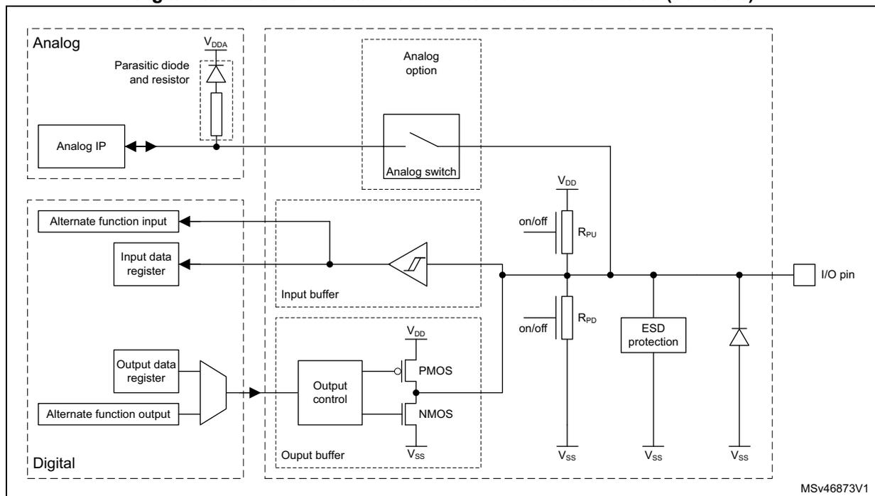
The diagram shows the internal circuitry of a GPIO pin. It is divided into Analog and Digital sections. - **Analog Section**: Contains an 'Analog IP' block connected to a 'Parasitic diode and resistor' network tied to V DDA . An 'Analog switch' (controlled by 'Analog option') connects the Analog IP to the I/O pin path. - **Digital Section**: - **Input Path**: Includes 'Alternate function input' and 'Input data register' connected via an 'Input buffer' (Schmitt trigger) to the I/O pin. - **Output Path**: Includes 'Output data register' and 'Alternate function output' feeding into an 'Output control' block. This block drives a CMOS output stage (PMOS and NMOS) in the 'Ouput buffer' (original typo preserved). The PMOS is tied to V DD and the NMOS to V SS . - **I/O Pin Interface**: The pin is connected to pull-up (R PU ) and pull-down (R PD ) resistors with on/off switches, an ESD protection block, and a diode to V SS . The external connection is labeled 'I/O pin'.
Note: On a TT GPIO, the analog switch is not present and replaced by a direct connection. The analog bloc parasitic circuitry does not allow five-volt tolerance.
Table 127. Port bit configuration (1)
| MODE(i)[1:0] | OTYPE(i) | OSPEED(i)[1:0] | PUPD(i)[1:0] | I/O configuration | ||
|---|---|---|---|---|---|---|
| 01 | 0 | SPEED[1:0] | 0 | 0 | GP output | PP |
| 0 | 0 | 1 | GP output | PP + PU | ||
| 0 | 1 | 0 | GP output | PP + PD | ||
| 0 | 1 | 1 | Reserved | |||
| 1 | 0 | 0 | GP output | OD | ||
| 1 | 0 | 1 | GP output | OD + PU | ||
| 1 | 1 | 0 | GP output | OD + PD | ||
| 1 | 1 | 1 | Reserved (GP output OD) | |||
| MODE(i)[1:0] | OTYPE(i) | OSPEED(i)[1:0] | PUPD(i)[1:0] | I/O configuration | |||
|---|---|---|---|---|---|---|---|
| 00 | 01 | 00 | 01 | ||||
| 10 | 0 | SPEED[1:0] | 0 | 0 | AF | PP | |
| 0 | 0 | 1 | AF | PP + PU | |||
| 0 | 1 | 0 | AF | PP + PD | |||
| 0 | 1 | 1 | Reserved | ||||
| 1 | 0 | 0 | AF | OD | |||
| 1 | 0 | 1 | AF | OD + PU | |||
| 1 | 1 | 0 | AF | OD + PD | |||
| 1 | 1 | 1 | Reserved | ||||
| 00 | x | x | x | 0 | 0 | Input | Floating |
| x | x | x | 0 | 1 | Input | PU | |
| x | x | x | 1 | 0 | Input | PD | |
| x | x | x | 1 | 1 | Reserved (input floating) | ||
| 11 | x | x | x | 0 | 0 | Input/output | Analog |
| x | x | x | 0 | 1 | Reserved | ||
| x | x | x | 1 | 0 | Input/Output | Analog | |
| x | x | x | 1 | 1 | Reserved | ||
1. GP = general-purpose, PP = push-pull, PU = pull-up, PD = pull-down, OD = open-drain, AF = alternate function.
13.3.1 General-purpose I/O (GPIO)
During and just after reset, the alternate functions are not active and most of the I/O ports are configured in analog mode.
The debug pins are in AF pull-up/pull-down after reset:
- • PA15: JTDI in pull-up
- • PA14: JTCK/SWCLK in pull-down
- • PA13: JTMS/SWDIO in pull-up
- • PB4: NJTRST in pull-up
- • PB3: JTDO/TRACE SWO in floating state no pull-up/pull-down
PH3/BOOT0 is in input mode during the reset until at least the end of the option byte loading phase (see Section 13.3.15 ).
When the pin is configured as output, the value written to the output data register (GPIOx_ODR) is output on the I/O pin. It is possible to use the output driver in push-pull mode or open-drain mode (only the low level is driven, the high level is high-Z).
The input data register (GPIOx_IDR) captures the data present on the I/O pin at every AHB clock cycle.
All GPIO pins have weak internal pull-up and pull-down resistors, that can be activated or not depending on the value in the GPIOx_PUPDR register.
13.3.2 I/O pin alternate function multiplexer and mapping
The device I/O pins are connected to on-board peripherals/modules through a multiplexer that allows only one peripheral alternate function (AF) connected to an I/O pin at a time. In this way, there is no conflict between peripherals available on the same I/O pin.
Each I/O pin has a multiplexer with up to 16 alternate function inputs (AF0 to AF15) that can be configured through the GPIOx_AFRL (for pin 0 to 7) and GPIOx_AFRH (for pin 8 to 15) registers:
- • After reset, the multiplexer selection is alternate function 0 (AF0). The I/Os are configured in alternate function mode through GPIOx_MODER register.
- • The specific alternate function assignments for each pin are detailed in the device datasheet.
In addition to this flexible I/O multiplexing architecture, each peripheral has alternate functions mapped onto different I/O pins to optimize the number of peripherals available in smaller packages.
To use an I/O in a given configuration, the user must proceed as follows:
- • Debug function: after each device reset, these pins are assigned as alternate function pins immediately usable by the debugger host.
- • GPIO: configure the desired I/O as output, input, or analog in GPIOx_MODER.
- •
Peripheral alternate function:
- – Connect the I/O to the desired AFx in one of GPIOx_AFRL or GPIOx_AFRH.
- – Select the type, pull-up/pull-down, and output speed via GPIOx_OTYPER, GPIOx_PUPDR, and GPIOx_OSPEEDR respectively.
- – Configure the desired I/O as an alternate function in GPIOx_MODER.
- •
Cortex-M33 alternate function (EVENTOUT):
- – The Cortex-M33 output EVENTOUT signal can be used by configuring the I/O to output at AF15. An event can be signaled through the configuring pin after executing SEV instruction.
- •
Additional functions:
- – For the ADC, DAC, OPAMP and COMP, configure the desired I/O in analog mode in GPIOx_MODER, and configure the required function in the ADC, DAC, OPAMP, and COMP registers.
- – For the additional functions like RTC, WKUPx, and oscillators, configure the required function in the related RTC, PWR, and RCC registers. These functions have priority over the configuration in the standard GPIO registers.
Refer to the “Alternate function mapping” table in the device datasheet for the detailed mapping of the alternate function I/O pins.
13.3.3 I/O port control registers
Each of the GPIO ports has four 32-bit memory-mapped control registers (GPIOx_MODER, GPIOx_OTYPER, GPIOx_OSPEEDR, GPIOx_PUPDR) to configure up to 16 I/Os:
- • GPIOx_MODER is used to select the I/O mode (input, output, AF, analog).
- • GPIOx_OTYPER and GPIOx_OSPEEDR are used to select the output type (push-pull or open-drain) and speed.
- • GPIOx_PUPDR is used to select the push-up/pull-down whatever the I/O direction.
13.3.4 I/O port data registers
Each GPIO has two 16-bit memory-mapped data registers: input and output data registers (GPIOx_IDR, x = A to J) and GPIOx_ODR, x = A to J).
GPIOx_ODR stores the data to be output, it is read/write accessible. The data input through the I/O are stored into GPIOx_IDR, a read-only register.
13.3.5 I/O data bitwise handling
The bit set reset register (GPIOx_BSRR) is a 32-bit register that allows the application to set and reset each individual bit in the output data register (GPIOx_ODR). The bit set reset register has twice the size of GPIOx_ODR.
To each bit in GPIOx_ODR, correspond two control bits in GPIOx_BSRR: BS(i) and BR(i). When written to 1, BS(i) sets the corresponding ODR(i) bit. When written to 1, BR(i) resets the ODR(i) corresponding bit.
Writing any bit to 0 in GPIOx_BSRR does not have any effect on the corresponding bit in GPIOx_ODR. If there is an attempt to both set and reset a bit in GPIOx_BSRR, the set action takes priority.
Using the GPIOx_BSRR register to change the values of individual bits in GPIOx_ODR is a “one-shot” effect that does not lock the GPIOx_ODR bits. The GPIOx_ODR bits can always be accessed directly. The GPIOx_BSRR register provides a way of performing atomic bitwise handling.
There is no need for the software to disable interrupts when programming the GPIOx_ODR at bit level: one or more bits can be modified in a single atomic AHB write access.
13.3.6 GPIO locking mechanism
The GPIO control registers can be frozen by applying a specific write sequence to the GPIOx_LCKR register. The frozen registers are GPIOx_MODER, GPIOx_OTYPER, GPIOx_OSPEEDR, GPIOx_PUPDR, GPIOx_AFRL, GPIOx_AFRH, and GPIOx_HSLVR.
To write GPIOx_LCKR, a specific write/read sequence must be applied. When the right LOCK sequence is applied to the bit 16 in this register, the value of LCKR[15:0] is used to lock the configuration of the I/Os (during the write sequence the LCKR[15:0] value must be the same). When the lock sequence is applied to a port bit, the value of the port bit can no longer be modified until the next MCU reset or peripheral reset. Each GPIOx_LCKR bit freezes the corresponding bit in the control registers (GPIOx_MODER, GPIOx_OTYPER, GPIOx_OSPEEDR, GPIOx_PUPDR, GPIOx_AFRL, and GPIOx_AFRH).
The lock sequence can only be performed using a word (32-bit long) access to GPIOx_LCKR due to the fact that GPIOx_LCKR bit 16 must be set at the same time as the [15:0] bits.
13.3.7 I/O alternate function input/output
Two registers are provided to select one of the alternate function inputs/outputs available for each I/O. With these registers, the user can connect an alternate function to some other pin as required by the application.
This means that a number of possible peripheral functions are multiplexed on each GPIO using GPIOx_AFRL and GPIOx_AFRH alternate function registers. The application can thus select any one of the possible functions for each I/O. The AF selection signal being
common to the alternate function input and alternate function output, a single channel is selected for the alternate function input/output of a given I/O.
To know which functions are multiplexed on each GPIO pin, refer to the device datasheet.
13.3.8 External interrupt/wake-up lines
All ports have external interrupt capability. To use external interrupt lines, the port can be configured in input, output, or alternate function mode (the port must not be configured in analog mode). Refer to Section 23: Extended interrupts and event controller (EXTI) .
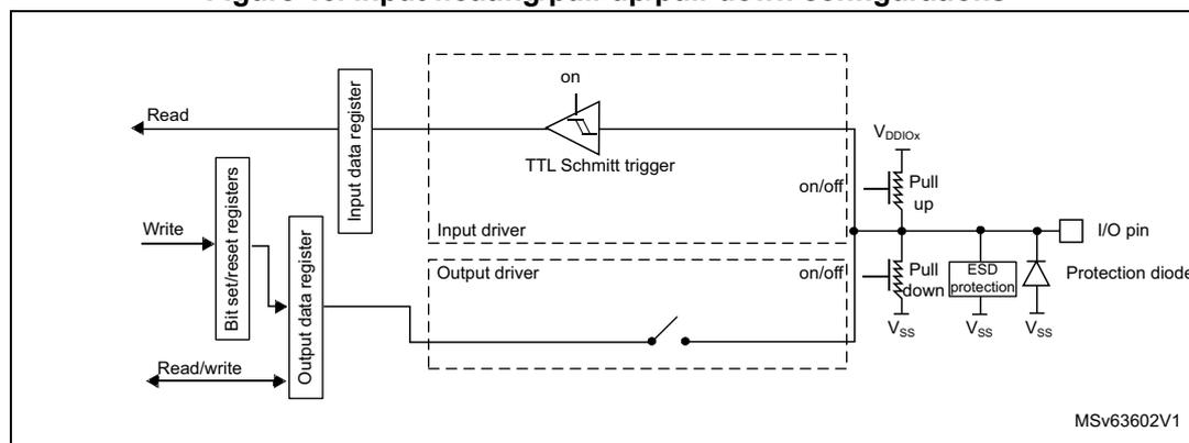
13.3.9 Input configuration
When the I/O port is programmed as input:
- • The output buffer is disabled.
- • The Schmitt trigger input is activated.
- • The pull-up and pull-down resistors are activated depending on the value in GPIOx_PUPDR.
- • The data present on the I/O pin are sampled into the input data register every AHB clock cycle.
- • A read access to the input data register provides the I/O state.
The figure below shows the input configuration of the I/O port bit.
Figure 46. Input floating/pull-up/pull-down configurations
13.3.10 Output configuration
When the I/O port is programmed as output:
- • The output buffer is enabled:
- – Open-drain mode: a 0 in the output register activates the N-MOS whereas a 1 in the output register leaves the port in Hi-Z (the P-MOS is never activated).
- – Push-pull mode: a 0 in the output register activates the N-MOS whereas a 1 in the output register activates the P-MOS.
- • The Schmitt trigger input is activated.
- • The pull-up and pull-down resistors are activated depending on the value in the GPIOx_PUPDR register.
- • The data present on the I/O pin are sampled into the input data register every AHB clock cycle.
- • A read access to the input data register gets the I/O state.
- • A read access to the output data register gets the last written value.
The figure below shows the output configuration of the I/O port bit.
Figure 47. Output configuration
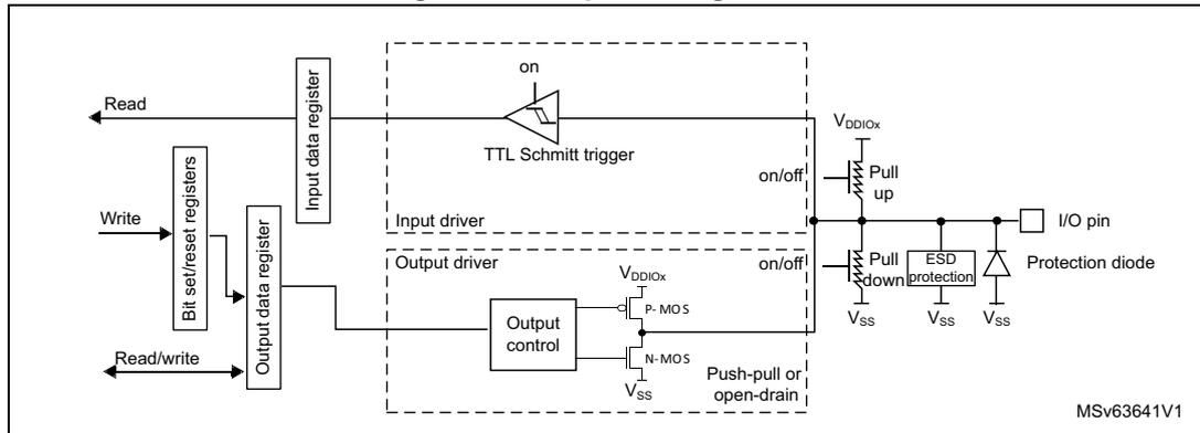
The diagram illustrates the internal architecture of an I/O pin in output mode. On the left, external signals are processed through registers: 'Read' from the pin to the 'Input data register', 'Write' to 'Bit set/reset registers', and 'Read/write' to the 'Output data register'. The 'Input driver' contains a 'TTL Schmitt trigger' connected to the 'Input data register'. The 'Output driver' consists of 'P-MOS' and 'N-MOS' transistors controlled by 'Output control', connected to the 'Output data register'. These transistors can be configured for 'Push-pull or open-drain' mode. Weak 'Pull up' and 'Pull down' resistors are connected to the pin, controlled by 'on/off' signals. The pin also features 'ESD protection' and a 'Protection diode' connected to 'V DDIOX ' and 'V SS '. The diagram is labeled 'MSv63641V1'.
13.3.11 Alternate function configuration
When the I/O port is programmed as the alternate function:
- • The output buffer can be configured in open-drain or push-pull mode.
- • The output buffer is driven by the signals coming from the peripheral (transmitter enable and data).
- • The Schmitt trigger input is activated.
- • The weak pull-up and pull-down resistors are activated or not depending on the value in the GPIOx_PUPDR register.
- • The data present on the I/O pin are sampled into the input data register every AHB clock cycle.
- • A read access to the input data register gets the I/O state.
The figure below shows the alternate function configuration of the I/O port bit.
Figure 48. Alternate function configuration
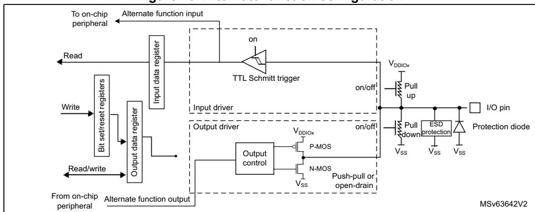
This diagram shows the internal circuitry for alternate function mode. The 'Input driver' with 'TTL Schmitt trigger' and 'Input data register' remains the same. The 'Output driver' (P-MOS/N-MOS) is now driven by 'Alternate function output' signals 'From on-chip peripheral' instead of the 'Output data register'. The 'Bit set/reset registers' and 'Output data register' are still present but the latter is not actively driving the pin. The 'Pull up', 'Pull down', 'ESD protection', and 'Protection diode' components are also shown, connected to the 'I/O pin'. The diagram is labeled 'MSv63642V2'.
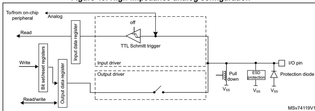
13.3.12 Analog configuration
When the I/O port is programmed as analog configuration:
- • The output buffer is disabled.
- • The Schmitt trigger input is deactivated, providing zero consumption for every analog value of the I/O pin. The output of the Schmitt trigger is forced to a constant value (0).
- • The weak pull-up resistors are disabled by hardware. The weak pull-down is configurable.
- • Read access to the input data register gets the value 0.
The figure below shows the high-impedance, analog-input configuration of the I/O port bits.
Figure 49. High-impedance analog configuration
13.3.13 Using the HSE or LSE oscillator pins as GPIOs
When the HSE or LSE oscillator is switched off (default state after reset), the related oscillator pins can be used as normal GPIOs.
When the HSE or LSE oscillator is switched on (by setting the HSEON or LSEON bit in the RCC_CR and RCC_BDCR registers), the oscillator takes control of its associated pins and the GPIO configuration of these pins has no effect.
When the oscillator is configured in a user external clock mode, only the pin is reserved for clock input, and the OSC_OUT or OSC32_OUT pin can still be used as normal GPIO.
13.3.14 Using the GPIO pins in the RTC supply domain
The PC13/PC14/PC15 GPIO functionality is lost when the core supply domain is powered off (when the device enters Standby mode). In this case, if their GPIO configuration is not bypassed by the RTC configuration, these pins are set in an analog input mode.
For details about I/O control by the RTC, refer to Section 63.3: RTC functional description
13.3.15 Using PH3 as GPIO
PH3 may be used as boot pin (BOOT0) or as a GPIO. Depending on the nSWBOOT0 bit in the user option byte, PH3 switches from the input mode to the analog input mode:
- • After the option byte loading phase if nSWBOOT0 = 1.
- • After reset if nSWBOOT0 = 0.
13.3.16 Using PA11 and PA12 as GPIOs (STM32U59x/5Ax/5Fx/5Gx only)
PA11 and PA12 provide OTG_HS additional functions. There are constraints to use PA11 and PA12 as standard GPIOs or alternate functions. Refer to Section 10.7.12: USB power management in low-power modes (STM32U59x/5Ax/5Fx/5Gx only) .
13.3.17 OPAMPx_VINM dedicated pins
The OPAMPx_VINM dedicated pins are three-volt tolerant and are supplied by V DDA . These pins do not feature a complete TT structure as shown in Figure 45 , but a direct connection to OPAMPx. The OPAMPx_VINM dedicated pins are available on specific packages only (refer to the device datasheet for availability of these pins).
13.3.18 TrustZone security
The TrustZone security is activated by the TZEN option bit in the FLASH_OPTR. When the TrustZone is active (TZEN = 1), each I/O pin of GPIO port can be individually configured as secure through the GPIOx_SECCFGR register.
When the selected I/O pin is configured as secure, its corresponding configuration bits for alternate function, mode selection, I/O data are secure against a nonsecure access. In case of nonsecure access, these bits are RAZ/WI. The GPIO clock and reset control bits in the RCC are automatically configured as secure as soon as at least one I/O in the GPIO is secure.
The I/Os with peripherals functions are also conditioned by the peripheral security configuration (see Section 5: Global TrustZone controller (GTZC) for more details):
- • For peripherals for which the I/O pin selection is done through alternate functions registers: if the peripheral is configured as secure, it cannot be connected to a nonsecure I/O pin. If this is not respected, the input data to the secure peripheral is forced to 0 (I/O input pin value is ignored) and the output pin value is forced to 0, thus avoiding any secure information leak through nonsecure I/Os.
- • For I/Os with analog switches, directly controlled by peripherals (such as ADC for instance): If the I/O is secure, the I/O analog switch cannot be controlled by a nonsecure peripheral. If this is not respected, the switch remains open. This prevent the redirection of secure data to a nonsecure peripheral or I/O through analog path. Refer to Section 3: System security for more details.
- • Some of the paths between I/Os “additional functions” and peripherals are not blocked if the I/O is secure and the peripheral is nonsecure. Therefore it is recommended to configure those peripherals as secure even when not used by the application. Refer to Section 3: System security for the list of concerned peripherals. When the path has a security control, it follows the same rule as I/O selection through alternate functions.
Refer to the device pins definition table in datasheet for more information about peripherals alternate functions and additional functions mapping.
After reset, all GPIO ports are secure.
Table 128 gives a summary of the I/O port secured bits following the security configuration bit in the GPIO_SECCFGR register. When the I/O bit port is configured as secure:
- • Secured bits: read and write operations are only allowed by a secure access. Non secure-read or write accesses on secured bits are RAZ/WI. There is no illegal access event generated.
- • Nonsecure bits: no restriction. Read and write operations are allowed by both secure and nonsecure accesses.
When the TrustZone security is disabled (TZEN = 0 in FLASH_OPTR register), all registers bits are nonsecure. The GPIOx_SECCFGR register is RAZ/WI.
Table 128. GPIO secured bits
| Secure configuration bit | Secured bit | Register name | Nonsecure access on secure bits |
|---|---|---|---|
| SECy = 1 in GPIOx_SECCFGR (1) | MODEy[1:0] | GPIOx_MODER | RAZ/WI |
| OTy | GPIOx_OTYPER | ||
| OSPEEDy[1:0] | GPIOx_OSPEEDR | ||
| PUPDy[1:0] | GPIOx_PUPDR | ||
| IDy | GPIOx_IDR | ||
| ODy | GPIOx_ODR | ||
| BSy and BRy | GPIOx_BSRR | ||
| LCKy | GPIOx_LCKR | ||
| BRy | GPIOx_BRR | ||
| AFSELy[3:0] | GPIOx_AFRH | ||
| GPIOx_AFRL | |||
| HSLVy | GPIOx_HSLVR |
1. The number of GPIOx ports varies in the STM32U5 Series devices. Refer to the product datasheet for availability of a particular port. If not present, consider the associated bits as reserved and keep them at the reset value.
13.3.19 Privileged and unprivileged modes
All GPIO registers can be read and written by privileged and unprivileged accesses, whatever the security state (secure or nonsecure).
13.3.20 High-speed low-voltage mode (HSLV)
Some I/Os have the capability to increase their maximum speed at low voltage by configuring them in HSLV mode. The I/O HSLV bit controls whether the I/O output speed is optimized to operate at 3.3 V (default setting) or at 1.8 V (HSLV = 1).
Caution: The I/O HSLV configuration bit must not be set if the I/O supply (V DD or V DDIO2 ) is above 2.7 V. Setting it while the voltage is higher than 2.7 V can damage the device. The I/O HSLV bit can be set only when the corresponding option bit is activated (IO_VDD_HSLV or IO_VDDIO2_HSLV depending on the I/O supply, refer to Section 7.4: FLASH option bytes ).
There is no hardware protection associated to this feature so it is recommended to use it only as a static configuration for fixed I/O supply.
Caution: Setting this bit when the I/O is configured in Fm+ mode is forbidden. An I/O is in Fm+ mode when it is configured as I2C alternate function, with FMP=1 in I2C_CR1 register. PB6, PB7, PB8, PB9 can also be in Fm+ mode when PB6_FMP, PB7_FMP, PB8_FMP, PB9_FMP, respectively, is set in SYSCFG_CFGR1 register.
Caution: On STM32U59x/5Ax/5Fx/5Gx devices, HSLVy bits in GPIOx_HLSVR must be programmed with the same value within the following pairs: PF4/PF5, PI3/PI4, or PI6/PI7. Each of these pairs can be used as a differential clock for the OCTOSPIs or HSPI, but this caution applies even if these pairs are used for other purposes.
13.3.21 I/O compensation cell
The I/O commutation slew rate ( \( t_{fall}/t_{rise} \) ) can be adapted by software depending on process, voltage, and temperatures conditions, in order to reduce the I/O noise on power supply. Refer to Section 15: System configuration controller (SYSCFG) for more details.
13.4 GPIO registers
This section gives a detailed description of the GPIO registers.
The peripheral registers can be written in word, half word or byte mode.
The number of GPIOx ports varies in the STM32U5 Series devices. Refer to the product datasheet for availability of a particular port. If not present, consider the associated bits as reserved and keep them at the reset value.
13.4.1 GPIO port mode register (GPIOx_MODER) (x = A to J)
Address offset: 0x00
Reset value: 0xABFF FFFF (for port A)
Reset value: 0xFFFF FEBF (for port B)
Reset value: 0xFFFF FFFF (for ports C..E)
Reset value: 0xFFFF FFFF (for port F on STM32U575/585/59x/5Ax/5Fx/5Gx)
Reset value: 0xFFFF FFF0 (for port G on STM32U535/545)
Reset value: 0xFFFF FFFF (for port G on STM32U575/585/59x/5Ax/5Fx/5Gx)
Reset value: 0x0000 00CF (for port H on STM32U535/545)
Reset value: 0xFFFF FFFF (for port H on STM32U575/585/59x/5Ax/5Fx/5Gx)
Reset value: 0x0000 FFFF (for port I on STM32U575/585)
Reset value: 0xFFFF FFFF (for port I on STM32U59x/5Ax/5Fx/5Gx)
Reset value: 0x00FF FFFF (for port J on STM32U59x/5Ax/5Fx/5Gx)
| 31 | 30 | 29 | 28 | 27 | 26 | 25 | 24 | 23 | 22 | 21 | 20 | 19 | 18 | 17 | 16 |
|---|---|---|---|---|---|---|---|---|---|---|---|---|---|---|---|
| MODE15[1:0] | MODE14[1:0] | MODE13[1:0] | MODE12[1:0] | MODE11[1:0] | MODE10[1:0] | MODE9[1:0] | MODE8[1:0] | ||||||||
| rw | rw | rw | rw | rw | rw | rw | rw | rw | rw | rw | rw | rw | rw | rw | rw |
| 15 | 14 | 13 | 12 | 11 | 10 | 9 | 8 | 7 | 6 | 5 | 4 | 3 | 2 | 1 | 0 |
| MODE7[1:0] | MODE6[1:0] | MODE5[1:0] | MODE4[1:0] | MODE3[1:0] | MODE2[1:0] | MODE1[1:0] | MODE0[1:0] | ||||||||
| rw | rw | rw | rw | rw | rw | rw | rw | rw | rw | rw | rw | rw | rw | rw | rw |
Bits 31:0 MODEy[1:0] : Port x configuration I/O pin y (y = 15 to 0)
These bits are written by software to configure the I/O mode.
00: Input mode
01: General purpose output mode
10: Alternate function mode
11: Analog mode (reset state)
Note: This field is reserved and must be kept at reset value when the corresponding I/O is not available on the selected package.
13.4.2 GPIO port output type register (GPIOx_OTYPER) (x = A to J)
Address offset: 0x04
Reset value: 0x0000 0000
| 31 | 30 | 29 | 28 | 27 | 26 | 25 | 24 | 23 | 22 | 21 | 20 | 19 | 18 | 17 | 16 |
|---|---|---|---|---|---|---|---|---|---|---|---|---|---|---|---|
| Res. | Res. | Res. | Res. | Res. | Res. | Res. | Res. | Res. | Res. | Res. | Res. | Res. | Res. | Res. | Res. |
| 15 | 14 | 13 | 12 | 11 | 10 | 9 | 8 | 7 | 6 | 5 | 4 | 3 | 2 | 1 | 0 |
| OT15 | OT14 | OT13 | OT12 | OT11 | OT10 | OT9 | OT8 | OT7 | OT6 | OT5 | OT4 | OT3 | OT2 | OT1 | OT0 |
| rw | rw | rw | rw | rw | rw | rw | rw | rw | rw | rw | rw | rw | rw | rw | rw |
Bits 31:16 Reserved, must be kept at reset value.
Bits 15:0 OTy : Port x configuration I/O pin y (y = 15 to 0)
These bits are written by software to configure the I/O output type.
0: Output push-pull (reset state)
1: Output open-drain
Note: This bit is reserved and must be kept at reset value when the corresponding I/O is not available on the selected package.
13.4.3 GPIO port output speed register (GPIOx_OSPEEDR) (x = A to J)
Address offset: 0x08
Reset value: 0x0C00 0000 (for port A)
Reset value: 0x0000 00C0 (for port B)
Reset value: 0x0000 0000 (for the other ports)
| 31 | 30 | 29 | 28 | 27 | 26 | 25 | 24 | 23 | 22 | 21 | 20 | 19 | 18 | 17 | 16 |
|---|---|---|---|---|---|---|---|---|---|---|---|---|---|---|---|
| OSPEED15[1:0] | OSPEED14[1:0] | OSPEED13[1:0] | OSPEED12[1:0] | OSPEED11[1:0] | OSPEED10[1:0] | OSPEED9[1:0] | OSPEED8[1:0] | ||||||||
| rw | rw | rw | rw | rw | rw | rw | rw | rw | rw | rw | rw | rw | rw | rw | rw |
| 15 | 14 | 13 | 12 | 11 | 10 | 9 | 8 | 7 | 6 | 5 | 4 | 3 | 2 | 1 | 0 |
| OSPEED7[1:0] | OSPEED6[1:0] | OSPEED5[1:0] | OSPEED4[1:0] | OSPEED3[1:0] | OSPEED2[1:0] | OSPEED1[1:0] | OSPEED0[1:0] | ||||||||
| rw | rw | rw | rw | rw | rw | rw | rw | rw | rw | rw | rw | rw | rw | rw | rw |
Bits 31:0 OSPEEDy[1:0] : Port x configuration I/O pin y (y = 15 to 0)
These bits are written by software to configure the I/O output speed.
00: Low speed
01: Medium speed
10: High speed
11: Very-high speed
Note: Refer to the device datasheet for the frequency specifications, and the power supply and load conditions for each speed.
This field is reserved and must be kept at reset value when the corresponding I/O is not available on the selected package.
13.4.4 GPIO port pull-up/pull-down register (GPIOx_PUPDR) (x = A to J)
Address offset: 0x0C
Reset value: 0x6400 0000 (for port A)
Reset value: 0x0000 0100 (for port B)
Reset value: 0x0000 0000 (for the other ports)
| 31 | 30 | 29 | 28 | 27 | 26 | 25 | 24 | 23 | 22 | 21 | 20 | 19 | 18 | 17 | 16 |
|---|---|---|---|---|---|---|---|---|---|---|---|---|---|---|---|
| PUPD15[1:0] | PUPD14[1:0] | PUPD13[1:0] | PUPD12[1:0] | PUPD11[1:0] | PUPD10[1:0] | PUPD9[1:0] | PUPD8[1:0] | ||||||||
| rw | rw | rw | rw | rw | rw | rw | rw | rw | rw | rw | rw | rw | rw | rw | rw |
| 15 | 14 | 13 | 12 | 11 | 10 | 9 | 8 | 7 | 6 | 5 | 4 | 3 | 2 | 1 | 0 |
| PUPD7[1:0] | PUPD6[1:0] | PUPD5[1:0] | PUPD4[1:0] | PUPD3[1:0] | PUPD2[1:0] | PUPD1[1:0] | PUPD0[1:0] | ||||||||
| rw | rw | rw | rw | rw | rw | rw | rw | rw | rw | rw | rw | rw | rw | rw | rw |
Bits 31:0 PUPDy[1:0] : Port x configuration I/O pin y (y = 15 to 0)
These bits are written by software to configure the I/O pull-up or pull-down
00: No pull-up, pull-down
01: Pull-up
10: Pull-down
11: Reserved
Note: This field is reserved and must be kept at reset value when the corresponding I/O is not available on the selected package.
13.4.5 GPIO port input data register (GPIOx_IDR) (x = A to J)
Address offset: 0x10
Reset value: 0x0000 XXXX
| 31 | 30 | 29 | 28 | 27 | 26 | 25 | 24 | 23 | 22 | 21 | 20 | 19 | 18 | 17 | 16 |
|---|---|---|---|---|---|---|---|---|---|---|---|---|---|---|---|
| Res. | Res. | Res. | Res. | Res. | Res. | Res. | Res. | Res. | Res. | Res. | Res. | Res. | Res. | Res. | Res. |
| 15 | 14 | 13 | 12 | 11 | 10 | 9 | 8 | 7 | 6 | 5 | 4 | 3 | 2 | 1 | 0 |
| ID15 | ID14 | ID13 | ID12 | ID11 | ID10 | ID9 | ID8 | ID7 | ID6 | ID5 | ID4 | ID3 | ID2 | ID1 | ID0 |
| r | r | r | r | r | r | r | r | r | r | r | r | r | r | r | r |
Bits 31:16 Reserved, must be kept at reset value.
Bits 15:0 IDy : Port x input data I/O pin y (y = 15 to 0)
These bits are read-only. They contain the input value of the corresponding I/O port.
Note: This bit is reserved and must be kept at reset value when the corresponding I/O is not available on the selected package.
13.4.6 GPIO port output data register (GPIOx_ODR) (x = A to J)
Address offset: 0x14
Reset value: 0x0000 0000
| 31 | 30 | 29 | 28 | 27 | 26 | 25 | 24 | 23 | 22 | 21 | 20 | 19 | 18 | 17 | 16 |
|---|---|---|---|---|---|---|---|---|---|---|---|---|---|---|---|
| Res. | Res. | Res. | Res. | Res. | Res. | Res. | Res. | Res. | Res. | Res. | Res. | Res. | Res. | Res. | Res. |
| 15 | 14 | 13 | 12 | 11 | 10 | 9 | 8 | 7 | 6 | 5 | 4 | 3 | 2 | 1 | 0 |
| OD15 | OD14 | OD13 | OD12 | OD11 | OD10 | OD9 | OD8 | OD7 | OD6 | OD5 | OD4 | OD3 | OD2 | OD1 | OD0 |
| rw | rw | rw | rw | rw | rw | rw | rw | rw | rw | rw | rw | rw | rw | rw | rw |
Bits 31:16 Reserved, must be kept at reset value.
Bits 15:0 ODy : Port output data I/O pin y (y = 15 to 0)
These bits can be read and written by software.
Note: For atomic bit set/reset, these bits can be individually set and/or reset by writing to GPIOx_BSRR or GPIOx_BRR (x = A to J).
This bit is reserved and must be kept at reset value when the corresponding I/O is not available on the selected package.
13.4.7 GPIO port bit set/reset register (GPIOx_BSRR) (x = A to J)
Address offset: 0x18
Reset value: 0x0000 0000
| 31 | 30 | 29 | 28 | 27 | 26 | 25 | 24 | 23 | 22 | 21 | 20 | 19 | 18 | 17 | 16 |
|---|---|---|---|---|---|---|---|---|---|---|---|---|---|---|---|
| BR15 | BR14 | BR13 | BR12 | BR11 | BR10 | BR9 | BR8 | BR7 | BR6 | BR5 | BR4 | BR3 | BR2 | BR1 | BR0 |
| w | w | w | w | w | w | w | w | w | w | w | w | w | w | w | w |
| 15 | 14 | 13 | 12 | 11 | 10 | 9 | 8 | 7 | 6 | 5 | 4 | 3 | 2 | 1 | 0 |
| BS15 | BS14 | BS13 | BS12 | BS11 | BS10 | BS9 | BS8 | BS7 | BS6 | BS5 | BS4 | BS3 | BS2 | BS1 | BS0 |
| w | w | w | w | w | w | w | w | w | w | w | w | w | w | w | w |
Bits 31:16 BRy : Port x reset I/O pin y (y = 15 to 0)
These bits are write-only. A read to these bits returns the value 0x0000.
0: No action on the corresponding ODy bit
1: Resets the corresponding ODy bit
Note: If both BSy and BRy are set, BSy has priority.
This bit is reserved and must be kept at reset value when the corresponding I/O is not available on the selected package.
Bits 15:0 BSy : Port x set I/O pin y (y = 15 to 0)
These bits are write-only. A read to these bits returns the value 0x0000.
0: No action on the corresponding ODy bit
1: Sets the corresponding ODy bit
Note: The bit is reserved and must be kept at reset value when the corresponding I/O is not available on the selected package.
13.4.8 GPIO port configuration lock register (GPIOx_LCKR) (x = A to J)
Address offset: 0x1C
Reset value: 0x0000 0000
This register is used to lock the configuration of the port bits when a correct write sequence is applied to bit 16 (LCKK). The value of bits [15:0] is used to lock the configuration of the GPIO. During the write sequence, the value of LCKR[15:0] must not change. When the LOCK sequence has been applied on a port bit, the value of this port bit can no longer be modified until the next MCU reset or peripheral reset.
Note: A specific write sequence is used to write to GPIOx_LCKR. Only word access (32-bit long) is allowed during this locking sequence.
Each lock bit freezes a specific configuration register (control and alternate function registers).
| 31 | 30 | 29 | 28 | 27 | 26 | 25 | 24 | 23 | 22 | 21 | 20 | 19 | 18 | 17 | 16 |
|---|---|---|---|---|---|---|---|---|---|---|---|---|---|---|---|
| Res. | Res. | Res. | Res. | Res. | Res. | Res. | Res. | Res. | Res. | Res. | Res. | Res. | Res. | Res. | LCKK |
| 15 | 14 | 13 | 12 | 11 | 10 | 9 | 8 | 7 | 6 | 5 | 4 | 3 | 2 | 1 | 0 |
| LCK15 | LCK14 | LCK13 | LCK12 | LCK11 | LCK10 | LCK9 | LCK8 | LCK7 | LCK6 | LCK5 | LCK4 | LCK3 | LCK2 | LCK1 | LCK0 |
| rw | rw | rw | rw | rw | rw | rw | rw | rw | rw | rw | rw | rw | rw | rw | rw |
Bits 31:17 Reserved, must be kept at reset value.
Bit 16 LCKK : Lock key
This bit can be read any time. It can only be modified using the lock key write sequence.
0: Port configuration lock key not active
1: Port configuration lock key active. The GPIOx_LCKR register is locked until the next MCU reset or peripheral reset.
- LOCK key write sequence:
WR LCKR[16] = 1 + LCKR[15:0]
WR LCKR[16] = 0 + LCKR[15:0]
WR LCKR[16] = 1 + LCKR[15:0]
- LOCK key read
RD LCKR[16] = 1 (this read operation is optional but it confirms that the lock is active)
Note: During the lock key write sequence, the value of LCK[15:0] must not change.
Any error in the lock sequence aborts the LOCK.
After the first lock sequence on any bit of the port, any read access on the LCKK bit returns 1 until the next MCU reset or peripheral reset.
Bits 15:0 LCKy : Port x lock I/O pin y (y = 15 to 0)
These bits are read/write but can only be written when the LCKK bit is 0
0: Port configuration not locked
1: Port configuration locked
Note: This bit is reserved and must be kept at reset value when the corresponding I/O is not available on the selected package.
13.4.9 GPIO alternate function low register (GPIOx_AFRL) (x = A to J)
Address offset: 0x20
Reset value: 0x0000 0000
| 31 | 30 | 29 | 28 | 27 | 26 | 25 | 24 | 23 | 22 | 21 | 20 | 19 | 18 | 17 | 16 |
|---|---|---|---|---|---|---|---|---|---|---|---|---|---|---|---|
| AFSEL7[3:0] | AFSEL6[3:0] | AFSEL5[3:0] | AFSEL4[3:0] | ||||||||||||
| rw | rw | rw | rw | rw | rw | rw | rw | rw | rw | rw | rw | rw | rw | rw | rw |
| 15 | 14 | 13 | 12 | 11 | 10 | 9 | 8 | 7 | 6 | 5 | 4 | 3 | 2 | 1 | 0 |
| AFSEL3[3:0] | AFSEL2[3:0] | AFSEL1[3:0] | AFSEL0[3:0] | ||||||||||||
| rw | rw | rw | rw | rw | rw | rw | rw | rw | rw | rw | rw | rw | rw | rw | rw |
Bits 31:0 AFSELy[3:0] : Alternate function selection for port x I/O pin y (y = 7 to 0)
These bits are written by software to configure alternate function I/Os.
0000: AF00001: AF1
0010: AF2
0011: AF3
0100: AF4
0101: AF5
0110: AF6
0111: AF7
1000: AF8
1001: AF9
1010: AF10
1011: AF11
1100: AF12
1101: AF13
1110: AF14
1111: AF15
Note: This field is reserved and must be kept at reset value when the corresponding I/O is not available on the selected package.
13.4.10 GPIO alternate function high register (GPIOx_AFRH) (x = A to J)
Address offset: 0x24
Reset value: 0x0000 0000
| 31 | 30 | 29 | 28 | 27 | 26 | 25 | 24 | 23 | 22 | 21 | 20 | 19 | 18 | 17 | 16 |
|---|---|---|---|---|---|---|---|---|---|---|---|---|---|---|---|
| AFSEL15[3:0] | AFSEL14[3:0] | AFSEL13[3:0] | AFSEL12[3:0] | ||||||||||||
| rw | rw | rw | rw | rw | rw | rw | rw | rw | rw | rw | rw | rw | rw | rw | rw |
| 15 | 14 | 13 | 12 | 11 | 10 | 9 | 8 | 7 | 6 | 5 | 4 | 3 | 2 | 1 | 0 |
| AFSEL11[3:0] | AFSEL10[3:0] | AFSEL9[3:0] | AFSEL8[3:0] | ||||||||||||
| rw | rw | rw | rw | rw | rw | rw | rw | rw | rw | rw | rw | rw | rw | rw | rw |
Bits 31:0 AFSELY[3:0] : Alternate function selection for port x I/O pin y (y = 15 to 8)
These bits are written by the software to configure alternate function I/Os.
0000: AF0
0001: AF1
0010: AF2
0011: AF3
0100: AF4
0101: AF5
0110: AF6
0111: AF7
1000: AF8
1001: AF9
1010: AF10
1011: AF11
1100: AF12
1101: AF13
1110: AF14
1111: AF15
Note: This field is reserved and must be kept at reset value when the corresponding I/O is not available on the selected package.
13.4.11 GPIO port bit reset register (GPIOx_BRR) (x = A to J)
Address offset: 0x28
Reset value: 0x0000 0000
| 31 | 30 | 29 | 28 | 27 | 26 | 25 | 24 | 23 | 22 | 21 | 20 | 19 | 18 | 17 | 16 |
|---|---|---|---|---|---|---|---|---|---|---|---|---|---|---|---|
| Res. | Res. | Res. | Res. | Res. | Res. | Res. | Res. | Res. | Res. | Res. | Res. | Res. | Res. | Res. | Res. |
| 15 | 14 | 13 | 12 | 11 | 10 | 9 | 8 | 7 | 6 | 5 | 4 | 3 | 2 | 1 | 0 |
| BR15 | BR14 | BR13 | BR12 | BR11 | BR10 | BR9 | BR8 | BR7 | BR6 | BR5 | BR4 | BR3 | BR2 | BR1 | BR0 |
| w | w | w | w | w | w | w | w | w | w | w | w | w | w | w | w |
Bits 31:16 Reserved, must be kept at reset value.
Bits 15:0 BRy : Port x reset IO pin y (y = 15 to 0)
These bits are write-only. A read to these bits returns the value 0x0000.
0: No action on the corresponding ODy bit
1: Reset the corresponding ODy bit
Note: This bit is reserved and must be kept at reset value when the corresponding I/O is not available on the selected package.
13.4.12 GPIO high-speed low-voltage register (GPIOx_HSLVR) (x = A to J)
Address offset: 0x2C
Reset value: 0x0000 0000
| 31 | 30 | 29 | 28 | 27 | 26 | 25 | 24 | 23 | 22 | 21 | 20 | 19 | 18 | 17 | 16 |
|---|---|---|---|---|---|---|---|---|---|---|---|---|---|---|---|
| Res. | Res. | Res. | Res. | Res. | Res. | Res. | Res. | Res. | Res. | Res. | Res. | Res. | Res. | Res. | Res. |
| 15 | 14 | 13 | 12 | 11 | 10 | 9 | 8 | 7 | 6 | 5 | 4 | 3 | 2 | 1 | 0 |
| HSLV 15 | HSLV 14 | HSLV 13 | HSLV 12 | HSLV 11 | HSLV 10 | HSLV9 | HSLV8 | HSLV7 | HSLV6 | HSLV5 | HSLV4 | HSLV3 | HSLV2 | HSLV1 | HSLV0 |
| rw | rw | rw | rw | rw | rw | rw | rw | rw | rw | rw | rw | rw | rw | rw | rw |
Bits 31:16 Reserved, must be kept at reset value.
Bits 15:0 HSLVy : Port x high-speed low-voltage configuration (y = 15 to 0)
These bits are written by software to optimize the I/O speed when the I/O supply is low.
Each bit is active only if the corresponding IO_VDD_HSLV/IO_VDDIO2_HSLV user option bit is set. It must be used only if the I/O supply voltage is below 2.7 V.
Setting these bits when the I/O supply (VDD or VDDIO2) is higher than 2.7 V may be destructive. Setting this bit when the I/O is configured in Fm+ mode is forbidden.
0: I/O speed optimization disabled
1: I/O speed optimization enabled
Note: Not all I/Os support the HSLV mode. Refer to the I/O structure in the corresponding datasheet for the list of I/Os supporting this feature. Other I/Os HSLV configuration must be kept at reset value.
This bit is reserved and must be kept at reset value when the corresponding I/O is not available on the selected package.
13.4.13 GPIO secure configuration register (GPIOx_SECCFGR) (x = A to J)
Address offset: 0x30
Reset value: 0x0000 FFFF (for ports A to E)
Reset value: 0x0000 FFFF (for port F on STM32U575/585/59x/5Ax/5Fx/5Gx)
Reset value: 0x0000 FFFC (for port G on STM32U535/545)
Reset value: 0x0000 FFFF (for port G on STM32U575/585/59x/5Ax/5Fx/5Gx)
Reset value: 0x0000 000B (for port H on STM32U535/545)
Reset value: 0x0000 FFFF (for port H on STM32U575/585/59x/5Ax/5Fx/5Gx)
Reset value: 0x0000 00FF (for port I on STM32U575/585)
Reset value: 0x0000 FFFF (for port I on STM32U59x/5Ax/5Fx/5Gx)
Reset value: 0x0000 0FFF (for port J on STM32U59x/5Ax/5Fx/5Gx)
When the system is secure (TZEN = 1), this register provides write access security and can be written only by a secure access. It is used to configure a selected I/O as secure. A nonsecure write access to this register is discarded.
When the system is not secure (TZEN = 0), this register is RAZ/WI.
| 31 | 30 | 29 | 28 | 27 | 26 | 25 | 24 | 23 | 22 | 21 | 20 | 19 | 18 | 17 | 16 |
|---|---|---|---|---|---|---|---|---|---|---|---|---|---|---|---|
| Res. | Res. | Res. | Res. | Res. | Res. | Res. | Res. | Res. | Res. | Res. | Res. | Res. | Res. | Res. | Res. |
| 15 | 14 | 13 | 12 | 11 | 10 | 9 | 8 | 7 | 6 | 5 | 4 | 3 | 2 | 1 | 0 |
| SEC15 | SEC14 | SEC13 | SEC12 | SEC11 | SEC10 | SEC9 | SEC8 | SEC7 | SEC6 | SEC5 | SEC4 | SEC3 | SEC2 | SEC1 | SEC0 |
| rw | rw | rw | rw | rw | rw | rw | rw | rw | rw | rw | rw | rw | rw | rw | rw |
Bits 31:16 Reserved, must be kept at reset value.
Bits 15:0 SEC y : I/O pin of Port x secure bit enable y (y = 15 to 0)
These bits are written by software to enable or disable the I/O port pin security.
0: The I/O pin is nonsecure
1: The I/O pin is secure. Refer to Table 128 for all corresponding secured bits.
Note: The bit is reserved and must be kept to reset value when the corresponding I/O is not available on the selected package.
13.4.14 GPIO register map
Table 129. GPIO register map and reset values
| Offset | Register name | 31 | 30 | 29 | 28 | 27 | 26 | 25 | 24 | 23 | 22 | 21 | 20 | 19 | 18 | 17 | 16 | 15 | 14 | 13 | 12 | 11 | 10 | 9 | 8 | 7 | 6 | 5 | 4 | 3 | 2 | 1 | 0 |
|---|---|---|---|---|---|---|---|---|---|---|---|---|---|---|---|---|---|---|---|---|---|---|---|---|---|---|---|---|---|---|---|---|---|
| 0x00 | GPIOx_MODER (x = A to J) | MODE15 [1:0] | MODE14 [1:0] | MODE13 [1:0] | MODE12 [1:0] | MODE11 [1:0] | MODE10 [1:0] | MODE9 [1:0] | MODE8 [1:0] | MODE7 [1:0] | MODE6 [1:0] | MODE5 [1:0] | MODE4 [1:0] | MODE3 [1:0] | MODE2 [1:0] | MODE1 [1:0] | MODE0 [1:0] | ||||||||||||||||
| Reset value for port A | 1 | 0 | 1 | 0 | 1 | 0 | 1 | 1 | 1 | 1 | 1 | 1 | 1 | 1 | 1 | 1 | 1 | 1 | 1 | 1 | 1 | 1 | 1 | 1 | 1 | 1 | 1 | 1 | 1 | 1 | 1 | 1 | |
| Reset value for port B | 1 | 1 | 1 | 1 | 1 | 1 | 1 | 1 | 1 | 1 | 1 | 1 | 1 | 1 | 1 | 1 | 1 | 1 | 1 | 1 | 1 | 1 | 1 | 0 | 1 | 0 | 1 | 1 | 1 | 1 | 1 | 1 | |
| Reset value for ports C...I | 1 | 1 | 1 | 1 | 1 | 1 | 1 | 1 | 1 | 1 | 1 | 1 | 1 | 1 | 1 | 1 | 1 | 1 | 1 | 1 | 1 | 1 | 1 | 1 | 1 | 1 | 1 | 1 | 1 | 1 | 1 | 1 | |
| Reset value for port J | 0 | 0 | 0 | 0 | 0 | 0 | 0 | 0 | 1 | 1 | 1 | 1 | 1 | 1 | 1 | 1 | 1 | 1 | 1 | 1 | 1 | 1 | 1 | 1 | 1 | 1 | 1 | 1 | 1 | 1 | 1 | 1 | |
Table 129. GPIO register map and reset values (continued)
| Offset | Register name | 31 | 30 | 29 | 28 | 27 | 26 | 25 | 24 | 23 | 22 | 21 | 20 | 19 | 18 | 17 | 16 | 15 | 14 | 13 | 12 | 11 | 10 | 9 | 8 | 7 | 6 | 5 | 4 | 3 | 2 | 1 | 0 | |
|---|---|---|---|---|---|---|---|---|---|---|---|---|---|---|---|---|---|---|---|---|---|---|---|---|---|---|---|---|---|---|---|---|---|---|
| 0x04 | GPIOx_OTYPER (x = A to J) | Res | Res | Res | Res | Res | Res | Res | Res | Res | Res | Res | Res | Res | Res | Res | Res | OT15 | OT14 | OT13 | OT12 | OT11 | OT10 | OT9 | OT8 | OT7 | OT6 | OT5 | OT4 | OT3 | OT2 | OT1 | OT0 | |
| Reset value | 0 | 0 | 0 | 0 | 0 | 0 | 0 | 0 | 0 | 0 | 0 | 0 | 0 | 0 | 0 | 0 | ||||||||||||||||||
| 0x08 | GPIOx_OSPEEDR (x = A to J) | OSPEED15 [1:0] | OSPEED14 [1:0] | OSPEED13 [1:0] | OSPEED12 [1:0] | OSPEED11 [1:0] | OSPEED10 [1:0] | OSPEED9 [1:0] | OSPEED8 [1:0] | OSPEED7 [1:0] | OSPEED6 [1:0] | OSPEED5 [1:0] | OSPEED4 [1:0] | OSPEED3 [1:0] | OSPEED2 [1:0] | OSPEED1 [1:0] | OSPEED0 [1:0] | |||||||||||||||||
| Reset value for port A | 0 | 0 | 0 | 0 | 1 | 1 | 0 | 0 | 0 | 0 | 0 | 0 | 0 | 0 | 0 | 0 | 0 | 0 | 0 | 0 | 0 | 0 | 0 | 0 | 0 | 0 | 0 | 0 | 0 | 0 | 0 | 0 | ||
| Reset value for port B | 0 | 0 | 0 | 0 | 0 | 0 | 0 | 0 | 0 | 0 | 0 | 0 | 0 | 0 | 0 | 0 | 0 | 0 | 0 | 0 | 0 | 0 | 0 | 0 | 1 | 1 | 0 | 0 | 0 | 0 | 0 | 0 | ||
| Reset value for ports C...J | 0 | 0 | 0 | 0 | 0 | 0 | 0 | 0 | 0 | 0 | 0 | 0 | 0 | 0 | 0 | 0 | 0 | 0 | 0 | 0 | 0 | 0 | 0 | 0 | 0 | 0 | 0 | 0 | 0 | 0 | 0 | 0 | ||
| 0x0C | GPIOx_PUPDR (x = A to J) | PUPD15 [1:0] | PUPD14 [1:0] | PUPD13 [1:0] | PUPD12 [1:0] | PUPD11 [1:0] | PUPD10 [1:0] | PUPD9 [1:0] | PUPD8 [1:0] | PUPD7 [1:0] | PUPD6 [1:0] | PUPD5 [1:0] | PUPD4 [1:0] | PUPD3 [1:0] | PUPD2 [1:0] | PUPD1 [1:0] | PUPD0 [1:0] | |||||||||||||||||
| Reset value for port A | 0 | 1 | 1 | 0 | 0 | 1 | 0 | 0 | 0 | 0 | 0 | 0 | 0 | 0 | 0 | 0 | 0 | 0 | 0 | 0 | 0 | 0 | 0 | 0 | 0 | 0 | 0 | 0 | 0 | 0 | 0 | 0 | ||
| Reset value for port B | 0 | 0 | 0 | 0 | 0 | 0 | 0 | 0 | 0 | 0 | 0 | 0 | 0 | 0 | 0 | 0 | 0 | 0 | 0 | 0 | 0 | 0 | 0 | 1 | 0 | 0 | 0 | 0 | 0 | 0 | 0 | 0 | ||
| Reset value for ports C...J | 0 | 0 | 0 | 0 | 0 | 0 | 0 | 0 | 0 | 0 | 0 | 0 | 0 | 0 | 0 | 0 | 0 | 0 | 0 | 0 | 0 | 0 | 0 | 0 | 0 | 0 | 0 | 0 | 0 | 0 | 0 | 0 | ||
| 0x10 | GPIOx_IDR (x = A to J) | Res | Res | Res | Res | Res | Res | Res | Res | Res | Res | Res | Res | Res | Res | Res | Res | ID15 | ID14 | ID13 | ID12 | ID11 | ID10 | ID9 | ID8 | ID7 | ID6 | ID5 | ID4 | ID3 | ID2 | ID1 | ID0 | |
| Reset value | X | X | X | X | X | X | X | X | X | X | X | X | X | X | X | X | ||||||||||||||||||
| 0x14 | GPIOx_ODR (x = A to J) | Res | Res | Res | Res | Res | Res | Res | Res | Res | Res | Res | Res | Res | Res | Res | Res | OD15 | OD14 | OD13 | OD12 | OD11 | OD10 | OD9 | OD8 | OD7 | OD6 | OD5 | OD4 | OD3 | OD2 | OD1 | OD0 | |
| Reset value | 0 | 0 | 0 | 0 | 0 | 0 | 0 | 0 | 0 | 0 | 0 | 0 | 0 | 0 | 0 | 0 | ||||||||||||||||||
| 0x18 | GPIOx_BRR (x = A to J) | BR15 | BR14 | BR13 | BR12 | BR11 | BR10 | BR9 | BR8 | BR7 | BR6 | BR5 | BR4 | BR3 | BR2 | BR1 | BR0 | BS15 | BS14 | BS13 | BS12 | BS11 | BS10 | BS9 | BS8 | BS7 | BS6 | BS5 | BS4 | BS3 | BS2 | BS1 | BS0 | |
| Reset value | 0 | 0 | 0 | 0 | 0 | 0 | 0 | 0 | 0 | 0 | 0 | 0 | 0 | 0 | 0 | 0 | 0 | 0 | 0 | 0 | 0 | 0 | 0 | 0 | 0 | 0 | 0 | 0 | 0 | 0 | 0 | 0 | ||
| 0x1C | GPIOx_LCKR (x = A to J) | Res | Res | Res | Res | Res | Res | Res | Res | Res | Res | Res | Res | Res | Res | Res | Res | LCKK | LCK15 | LCK14 | LCK13 | LCK12 | LCK11 | LCK10 | LCK9 | LCK8 | LCK7 | LCK6 | LCK5 | LCK4 | LCK3 | LCK2 | LCK1 | LCK0 |
| Reset value | 0 | 0 | 0 | 0 | 0 | 0 | 0 | 0 | 0 | 0 | 0 | 0 | 0 | 0 | 0 | 0 | ||||||||||||||||||
| 0x20 | GPIOx_AFRL (x = A to J) | AFSEL7[3:0] | AFSEL6[3:0] | AFSEL5[3:0] | AFSEL4[3:0] | AFSEL3[3:0] | AFSEL2[3:0] | AFSEL1[3:0] | AFSEL0[3:0] | |||||||||||||||||||||||||
| Reset value | 0 | 0 | 0 | 0 | 0 | 0 | 0 | 0 | 0 | 0 | 0 | 0 | 0 | 0 | 0 | 0 | 0 | 0 | 0 | 0 | 0 | 0 | 0 | 0 | 0 | 0 | 0 | 0 | 0 | 0 | 0 | 0 | ||
| 0x24 | GPIOx_AFRH (x = A to J) | AFSEL15 [3:0] | AFSEL14 [3:0] | AFSEL13 [3:0] | AFSEL12 [3:0] | AFSEL11[3:0] | AFSEL10 [3:0] | AFSEL9[3:0] | AFSEL8[3:0] | |||||||||||||||||||||||||
| Reset value | 0 | 0 | 0 | 0 | 0 | 0 | 0 | 0 | 0 | 0 | 0 | 0 | 0 | 0 | 0 | 0 | 0 | 0 | 0 | 0 | 0 | 0 | 0 | 0 | 0 | 0 | 0 | 0 | 0 | 0 | 0 | 0 | ||
| 0x28 | GPIOx_BRR (x = A to J) | Res | Res | Res | Res | Res | Res | Res | Res | Res | Res | Res | Res | Res | Res | Res | Res | BR15 | BR14 | BR13 | BR12 | BR11 | BR10 | BR9 | BR8 | BR7 | BR6 | BR5 | BR4 | BR3 | BR2 | BR1 | BR0 | |
| Reset value | 0 | 0 | 0 | 0 | 0 | 0 | 0 | 0 | 0 | 0 | 0 | 0 | 0 | 0 | 0 | 0 | ||||||||||||||||||
| 0x2C | GPIOx_HSLVR (x = A to J) | Res | Res | Res | Res | Res | Res | Res | Res | Res | Res | Res | Res | Res | Res | Res | Res | HSLV15 | HSLV14 | HSLV13 | HSLV12 | HSLV11 | HSLV10 | HSLV9 | HSLV8 | HSLV7 | HSLV6 | HSLV5 | HSLV4 | HSLV3 | HSLV2 | HSLV1 | HSLV0 | |
| Reset value | 0 | 0 | 0 | 0 | 0 | 0 | 0 | 0 | 0 | 0 | 0 | 0 | 0 | 0 | 0 | 0 | ||||||||||||||||||
| 0x30 | GPIOx_SECCFGR (x = A to J) | Res | Res | Res | Res | Res | Res | Res | Res | Res | Res | Res | Res | Res | Res | Res | Res | SEC15 | SEC14 | SEC13 | SEC12 | SEC11 | SEC10 | SEC9 | SEC8 | SEC7 | SEC6 | SEC5 | SEC4 | SEC3 | SEC2 | SEC1 | SEC0 | |
| Reset value for A to I | 1 | 1 | 1 | 1 | 1 | 1 | 1 | 1 | 1 | 1 | 1 | 1 | 1 | 1 | 1 | 1 | ||||||||||||||||||
| Reset value for port J | 0 | 0 | 0 | 0 | 1 | 1 | 1 | 1 | 1 | 1 | 1 | 1 | 1 | 1 | 1 | 1 |