11. Reset and clock control (RCC)
11.1 RCC introduction
The reset and clock control (RCC) manages the different kind of reset, and generates all clocks for the bus and peripherals.
11.2 RCC pins and internal signals
The table below lists the RCC inputs and output signals connected to package pins or balls.
Table 112. RCC input/output signals connected to package pins or balls
| Signal name | Signal type | Description |
|---|---|---|
| NRST | I/O | System reset, can be used to provide reset to external devices |
| OSC32_IN | I | 32 kHz oscillator input |
| OSC32_OUT | O | 32 kHz oscillator output |
| OSC_IN | I | System oscillator input |
| OSC_OUT | O | System oscillator output |
| MCO | O | Output clock for external devices |
| LSCO | O | Low-speed output clock for external devices |
| AUDIOCLK | I | External kernel clock input for SAI1, SAI2, MDF1 and ADF1 |
11.3 RCC reset functional description
There are three types of reset:
- • a system reset
- • a power reset
- • a backup domain reset
11.3.1 Power reset
A power reset is generated when one of the following events occurs:
- • a brownout reset (BOR)
- • when exiting Standby mode
- • when exiting Shutdown mode
A BOR sets all registers to their reset values except the ones in the backup domain.
When exiting Standby mode, all registers in the core domain are set to their reset value. Registers outside the core domain (RTC, TAMP, WKUP, IWDG, and Standby/Shutdown mode control) are not impacted.
When exiting Shutdown mode, a brownout reset is generated, resetting all registers except those in the backup domain.
11.3.2 System reset
A system reset sets all registers to their reset values except the reset flags in RCC_CSR, and the registers in the backup domain.
A system reset is generated when one of the following events occurs:
- • a low level on the NRST pin (external reset)
- • a window watchdog event (WWDG reset)
- • an independent watchdog event (IWDG reset)
- • a software reset (SW reset) (see Software reset )
- • a low-power mode security reset (see Low-power mode security reset )
- • an option-byte loader reset (see Option byte loader reset )
- • a brownout reset
The reset source can be identified by checking the reset flags in RCC_CSR.
These sources act on the NRST pin and this pin is always kept low during the delay phase. The reset service routine vector is selected via the boot option bytes.
The system reset signal provided to the device is output on the NRST pin. The pulse generator guarantees a minimum reset pulse duration of 20 µs for each internal reset source. In case of an external reset, the reset pulse is generated while the NRST pin is asserted low.
In case of an internal reset, the internal pull-up \( R_{PU} \) is deactivated in order to save the power consumption through the pull-up resistor.
Figure 37. Simplified diagram of the reset circuit
Software reset
The SYSRESETREQ bit in Cortex-M33 application interrupt and reset control register must be set to force a software reset on the device.
Low-power mode security reset
To avoid that critical applications mistakenly enter a low-power mode, the following low-power mode security resets are available. If enabled in option bytes, the resets are generated in any of the following conditions:
- • Entering Standby mode: this type of reset is enabled by resetting NRST_STDBY bit in user option bytes. In this case, whenever a Standby mode entry sequence is successfully executed, the device is reset instead of entering Standby mode.
- • Entering Stop mode: this type of reset is enabled by resetting NRST_STOP bit in user option bytes. In this case, whenever a Stop mode entry sequence is successfully executed, the device is reset instead of entering Stop mode.
- • Entering Shutdown mode: this type of reset is enabled by resetting NRST_SHDW bit in user option bytes. In this case, whenever a Shutdown mode entry sequence is successfully executed, the device is reset instead of entering Shutdown mode.
For further information on the user option bytes, refer to Section 7.4.1: Option bytes description .
Option byte loader reset
The option byte loader reset is generated when the OBL_LAUNCH bit is set in the FLASH_NSCR register. This bit is used to launch the option byte loading by software.
11.3.3 Backup domain reset
The backup domain has two specific resets.
A backup domain reset is generated when one of the following events occurs:
- • a software reset, triggered by setting BDRST bit RCC_BDCR
- • a V DD or V BAT power on, if both supplies have previously been powered off
A backup domain reset affects the LSE oscillator, the RTC, the TAMP, the backup registers, RCC_BDCR, and PWR_BDCR1. The reset of PWR_BDCR1 affects the backup SRAM. Backup domain reset caused by power on resets SRAM2 to zero as it is corresponding to a tamper policy.
11.4 RCC clock functional description
Four different clock sources can be used to drive the system clock (SYSCLK):
- • HSI16: high-speed internal 16 MHz RC oscillator clock
- • MSIS: multi-speed internal RC oscillator clock
- • HSE: high-speed external crystal or clock, from 4 to 50 MHz
- • PLL1 clock
The MSIS is used as system clock source after startup from reset, configured at 4 MHz.
The devices have the following additional clock sources:
- • MSIK: multi-speed internal RC oscillator clock used for peripherals kernel clocks
- • LSI: 32 kHz/250 Hz low-speed internal RC that drives the independent watchdog and optionally the RTC used for auto-wake-up from Stop and Standby modes
- • LSE: 32.768 kHz low-speed external crystal or clock that optionally drives the real-time clock (rtc_ck)
- • HSI48: internal 48 MHz RC that potentially drives the OTG_FS, the USB, the SDMMC, and the RNG
- • SHSI: secure high-speed internal 48 MHz RC that drives the SAES
- • PLL2 and PLL3 clocks
Each clock source can be switched on or off independently when it is not used, to optimize power consumption.
Several prescalers can be used to configure the AHB frequency, the APB1, APB2, and APB3 domains. The maximum frequency of the AHB and APB domains is 160 MHz.
All the peripheral clocks are derived from their bus clock (HCLK, PCLK1, PCLK2, or PCLK3) except the following ones that receive an independent kernel clock. This kernel clock can be selected by software between several sources thanks to RCC_CCIPRx registers ( \( x = 1, 2, 3 \) ): OTG_FS, USB, or OTG_HS, SDMMCx ( \( x = 1, 2 \) ), RNG, ADCx ( \( x = 1, 2, 4 \) ), DAC1, U(S)ARTx ( \( x = 1 \) to 6), LPUART1, I2Cx ( \( x = 1 \) to 6), SPIx ( \( x = 1 \) to 3), OCTOSPIx ( \( x = 1, 2 \) ), SAIx ( \( x = 1, 2 \) ), MDF1, ADF1, FDCAN1, LPTIMx ( \( x = 1 \) to 4), SAES, DSI, LTDC, HSPI1.
In addition, the RTC kernel clock is selected by software in RCC_BDCR. The IWDG clock is always the LSI 32 kHz clock.
The RCC feeds the Cortex system timer (SysTick) external clock with the AHB clock (HCLK) divided by eight, or LSE or LSI. The SysTick can work either with this clock or directly with the Cortex clock (HCLK), configurable in the SysTick control and status register.
FCLK acts as Cortex-M33 free-running clock.
Figure 38. Clock tree for STM32U5 series
The diagram illustrates the clock tree for the STM32U5 series. It shows the following components and connections:
- External Oscillators:
- LSI RC: 32 kHz or 250 Hz, connected to LSCO and LSI.
- LSE OSC: 32.768 kHz, connected to OSC32_IN, OSC32_OUT, and LSE.
- HSE OSC: 4-50 MHz, connected to OSC_IN, OSC_OUT, and HSE.
- Internal Oscillators:
- HSI RC: 16 MHz, connected to HSI16.
- MSI RC: 100 kHz – MHz, connected to MSIS.
- MSIK: 100 kHz – MHz, connected to MSIK.
- HSI48 RC: 48 MHz, connected to HSI48.
- SHSI RC: connected via /2 prescaler.
- PLLs:
- PLL1: VCO with /P, /Q, /N dividers. Outputs: pll1_p_ck, pll1_q_ck, pll1_r_ck. Includes a /M prescaler and a /MBOOST output to EPOD.
- PLL2: VCO with /P, /Q, /N dividers. Outputs: pll2_p_ck, pll2_q_ck, pll2_r_ck. Includes a /M prescaler.
- PLL3: VCO with /P, /Q, /N dividers. Outputs: pll3_p_ck, pll3_q_ck, pll3_r_ck. Includes a /M prescaler.
- Clock Source Control: Selects between LSE, LSI, MSIS, HSI16, HSE, SYSCLK, pll1_r_ck, HSI48, and MSIK.
- AHB Prescaler: /1,2,...,512, outputting HCLK to the AHB bus, core, memory, and DMA.
- APB1 Prescaler: /1,2,4,8,16, outputting PCLK1 to APB1 peripherals.
- APB2 Prescaler: /1,2,4,8,16, outputting PCLK2 to APB2 peripherals.
- APB3 Prescaler: /1,2,4,8,16, outputting PCLK3 to APB3 peripherals.
- Other Connections:
- Audio: AUDIOCLK, ICLK (from pll1_q_ck, pll2_q_ck, HSI16) to ADF1 and MDF1.
- Display/Interface: SYSCLK, pll1_q_ck, pll2_q_ck, pll3_r_ck to HSPI, LTDC, DSI (via DSI PHY PLL).
- USB: HSE, pll1_p_ck/2 to OTG_HS PHY PLL.
- ADCs: LSI, LSE to ADC1, ADC2, ADC4 and DAC1.
- Other Peripherals: Connections to IWDG, UCPD1, RTC/TAMP, LPTIM1, LPTIM3, LPTIM4, Cortex system timer, TIMx, USARTx, SPI2, I2Cx, LPTIM2, FDCAN1, CRS clock, OCTOSPIx, SAES, USART1, SPI1, SAix, SDMMCx, RNG, I2C3, SPI3, LPUART1.
Highlighted connections or peripheral may not be present in all devices of the STM32U5 Series.
Refer to the device datasheet for more information.
MSV71110V4
11.4.1 HSE clock
The high-speed external clock signal (HSE) can be generated from two possible clock sources:
- • HSE external crystal/ceramic resonator
- • HSE user external clock
The resonator and the load capacitors must be placed as close as possible to the oscillator pins in order to minimize output distortion and startup stabilization time. The loading capacitance values must be adjusted according to the selected oscillator.
Figure 39. HSE/ LSE clock sources
| Clock source | Hardware configuration |
|---|---|
| External clock | |
| Crystal/ceramic resonators |
External crystal/ceramic resonator (HSE crystal)
The 4 to 50 MHz external oscillator has the advantage of producing a very accurate rate on the main clock.
The associated hardware configuration is shown in Figure 39 . Refer to the electrical characteristics section of the datasheet for more details.
HSERDY in RCC_CR indicates if the HSE oscillator is stable or not. At startup, the clock is not released until this bit is set by hardware. An interrupt can be generated if enabled in RCC_CIER.
The HSE crystal can be switched on and off using HSEON in RCC_CR.
External source (HSE bypass)
In this mode, an external clock source must be provided. It can have a frequency of up to 50 MHz. This mode is selected by setting HSEBYP and HSEON in RCC_CR. The external clock signal (square, sinus, or triangle) with ~40-60 % duty cycle depending on the frequency (refer to the datasheet) must drive the OSC_IN pin while the OSC_OUT pin can be used a GPIO (see Figure 39 ).
11.4.2 HSI16 clock
The HSI16 clock signal is generated from an internal 16 MHz RC oscillator.
The HSI16 RC oscillator has the advantage of providing a clock source at low cost (no external components). It also has a faster startup time than the HSE crystal oscillator. However, even with calibration, the frequency is less accurate than an external crystal oscillator or ceramic resonator.
The HSI16 clock can be selected as system clock after wake-up from Stop modes. Refer to Section 11.8.6 . It can also be used as a backup clock source (auxiliary clock) if the HSE crystal oscillator fails. Refer to Section 11.4.11 .
Calibration
The RC oscillator frequencies may vary from one chip to another due to manufacturing process variations, this is why each device is factory calibrated by ST for 1 % accuracy at \( T_A = 25^\circ\text{C} \) .
After reset, the factory calibration value is loaded in HSICAL[7:0] of RCC_ICSCR3.
If the application is subject to voltage or temperature variations, this may affect the RC oscillator speed. The HSI16 frequency can be trimmed in the application using HSITRIM[6:0] in RCC_ICSCR3.
For more details on how to measure the HSI16 frequency variation, refer to Section 11.4.23 .
HSIRDY in RCC_CR indicates if the HSI16 RC is stable or not. At startup, the HSI16 RC output clock is not released until this bit is set by hardware.
The HSI16 RC can be switched on and off using HSION in RCC_CR.
The HSI16 signal can also be used as a backup source (auxiliary clock) if the HSE crystal oscillator fails. Refer to Section 11.4.11 .
11.4.3 MSI (MSIS and MSIK) clocks
The MSI is made of four internal RC oscillators: MSIRC0 at 48 MHz, MSIRC1 at 4 MHz, MSIRC2 at 3.072 MHz, and MSIRC3 at 400 kHz. Each oscillator feeds a prescaler providing a division by 1, 2, 3, or 4. Two output clocks are generated from these divided oscillators: MSIS that can be selected as system clock, and MSIK that can be selected by some peripherals as kernel clock.
Figure 40. MSI block diagram
Refer to datasheet for complete MSI frequency characteristics in MSI-mode and in PLL-mode. MSIS and MSIK frequency ranges can be adjusted by software, by using respectively MSISRANGE[3:0] and MSIKRANGE[3:0] in RCC_ICSCR1, with MSIRGSEL = 1. Sixteen frequency ranges are available, generated from the four internal RCs, as shown in the table below.
Table 113. MSIS and MSIK ranges per internal MSIRCs (PLL_mode disabled) (1)
| MSIRC0 | MSIRC1 | MSIRC2 | MSIRC3 |
|---|---|---|---|
| Range 0: 48 MHz | Range 4: 4 MHz | Range 8: 3.072 MHz | Range 12: 400 kHz |
| Range 1: 24 MHz | Range 5: 2 MHz | Range 9: 1.536 MHz | Range 13: 200 kHz |
| Range 2: 16 MHz | Range 6: 1.33 MHz | Range 10: 1.024 MHz | Range 14: 133 kHz |
| Range 3: 12 MHz | Range 7: 1 MHz | Range 11: 0.768 MHz | Range 15: 100 kHz |
1. Refer to datasheet for complete MSI frequency characteristics in MSI-mode and in PLL-mode.
The MSIS clock is used as system clock after restart from reset, wake-up from Standby, and Shutdown low-power modes. After restart from reset or when exiting Shutdown mode, MSIS and MSIK frequencies are set to their default value 4 MHz. The frequency range at wake-up from Standby mode can be adjusted by software, using respectively MSISSRANGE[3:0] and MSIKSRANGE[3:0] with MSIRGSEL = 0 (refer to RCC_CSR).
The MSIS clock can be selected as system clock after a wake-up from Stop mode (Stop 0, Stop 1, Stop 2, or Stop 3) depending on STOPWUCK in RCC_CR. It can also be used as a backup clock source (auxiliary clock) if the HSE crystal oscillator fails. See Section 11.4.11 .
The MSI advantage is to provide a low-cost (no external components) low-power clock source. In addition, when used in PLL-mode with the LSE, the MSI provides a very accurate clock source that can be used by the OTG_FS, or the USB, and feeds the PLL.
MSISRDY and MSIKRDY in RCC_CR indicate whether the MSIS and MSIK RC are stable or not. At startup, MSIS and MSIK RC output clocks are not released until their respective bit is set by hardware. The MSIS and MSIK RC can be switched on and off by using MSISON and MSIKON in RCC_CR.
Hardware auto calibration with LSE (PLL-mode)
When a 32.768 kHz external oscillator is present in the application, it is possible to configure either the MSIS or the MSIK in a PLL-mode. This mode is enabled:
- • for MSIS by setting MSIPLLEN with MSIPLLSEL = 1 in RCC_CR
- • for MSIK by setting MSIPLLEN with MSIPLLSEL = 0
In case MSIS and MSIK ranges are generated from the same MSIRC source, the PLL-mode is applied on both MSIS and MSIK. When configured in PLL-mode, the MSIS or MSIK automatically calibrates itself thanks to the LSE. This mode is available for all MSI frequency ranges. At 48 MHz, the MSIK in PLL-mode can be used for the OTG_FS, or the USB, avoiding the need of an external high-speed crystal.
If LSE clocks pulses are stopped, the MSI PLL-mode is automatically unlocked, and the MSI accuracy is consequently degraded. On all STM32U5 devices except STM32U575/585 rev. X, the MSI PLL-mode unlock event is connected to an EXTI line: this is used to generate an event or interrupt supporting wake-up from Stop 0, Stop 1, or Stop 2 mode (see Table 118: Interrupt sources and control and Table 189: EXTI line connections ).
MSI PLL-mode stabilization time
When MSIPLLEN = 1, the final accuracy after enabling the MSI (by writing MSISON = 1 or MSIKON = 1 or following a peripheral clock request in Stop mode) is reached after a stabilization time \( t_{\text{STAB}}(\text{MSI}) \) when MSIPLLFAST = 0. This stabilization time is needed even if the LSE is kept enable. Refer to datasheet for \( t_{\text{STAB}}(\text{MSI}) \) value.
If MSIPLLEN = 1 with MSIPLLFAST = 1, the MSI oscillator is kept powered on when a request to switch it off is received (either by writing MSISON = 0 and MSIKON = 0, or because no peripheral requests this clock in Stop mode). In this case the MSI PLL-mode accuracy is kept when the MSI is switched on again, providing that the \( t_{\text{STAB}}(\text{MSI}) \) stabilization time is reached before switching off the MSI. This mode can be used for autonomous peripherals requiring accuracy in Stop mode, with an extra consumption as the oscillator remains powered on, but gated off when disabled.
Software calibration
The MSIRCx (x = 0 to 3) oscillators frequency may vary from one chip to another due to manufacturing process variations, this is why each device is factory calibrated by ST for 1 % accuracy at an ambient temperature, \( T_A = 25\text{ }^\circ\text{C} \) . After reset, the factory calibration value is loaded in MSICALx[4:0] (x = 0 to 3) in RCC_ICSCR1. If the application is subject to voltage or temperature variations, this may affect the RC oscillator speed. The MSIRCx frequency can be trimmed in the application by using MSITRIMx[4:0] (x = 0 to 3) in RCC_ICSCR.
Note: The final accuracy after applying the calibration value is reached after a stabilization time. This stabilization time is needed after reset of exiting Standby or Shutdown mode. It is also needed when switching from PLL-mode to normal mode.
The hardware auto calibration with LSE must not be used in conjunction with software calibration.
For more details on how to measure the MSI frequency variation, refer to Section 11.4.23 .
11.4.4 HSI48 clock
The HSI48 clock signal is generated from an internal 48 MHz RC oscillator and can be used directly for USB/OTG_FS, and for the RNG, as well as the SDMMC.
The internal 48 MHz RC oscillator is mainly dedicated to provide a high-precision clock to the OTG_FS and the USB by means of a special clock recovery system (CRS) circuitry. The CRS can use the USB SOF signal (only on STM32U535/545/575/585), the LSE, or an external signal to automatically and quickly adjust the oscillator frequency on-the-fly. It is disabled as soon as the system enters Stop or Standby mode. When the CRS is not used, the HSI48 RC oscillator runs on its default frequency that is subject to manufacturing process variations.
For more details on how to configure and use the CRS peripheral, refer to Section 12: Clock recovery system (CRS) .
The HSI48RDY flag in the RCC_CR register indicates whether the HSI48 RC oscillator is stable or not. At startup, the HSI48 RC oscillator output clock is not released until this bit is set by hardware.
The HSI48 can be switched on and off using the HSI48ON bit in the RCC_CR register.
11.4.5 SHSI clock
The SHSI is an internal securable RC oscillator dedicated to clock the SAES. SHSIRDY flag in RCC_CR indicates if the SHSI RC is stable or not. At startup, the SHSI RC output clock is not released until this bit is set by hardware.
The SHSI RC can be switched on and off using SHSION in RCC_CR.
11.4.6 PLL
The RCC features three PLLs:
- • a main PLL, PLL1, that is generally used to provide clocks to the CPU and to some peripherals
- • two dedicated PLL2 and PLL3 that are used to generate the kernel clock for peripherals
The PLLs integrated into the RCC are completely independent. They offer the following features:
- • Input frequency range: 4 to 16 MHz
- • Capability to work either in integer or fractional mode
- • 13-bit sigma-delta ( \( \Sigma\Delta \) ) modulator, allowing to fine-tune the VCO frequency by steps of 11 to 0.3 ppm
- • The \( \Sigma\Delta \) modulator can be updated on-the-fly, without generating frequency overshoots on PLLs outputs.
- • Each PLL offers three outputs with post-dividers.
The PLLs are controlled via RCC_PLLxDIVR, RCC_PLLxFRACR, RCC_PLLxCFGR, and RCC_CR (x = 1, 2, 3).
The frequency of the reference clock provided to the PLLs (refx_ck) must range from 4 to 16 MHz. The user application must program properly the PLLxM (x = 1, 2, 3) dividers in RCC_PLL1CFGR, RCC_PLL2CFGR, and RCC_PLL3CFGR, in order to match this condition. In addition, PLLxRGE must be set according to the reference input frequency to guarantee an optimal performance of the PLL.
To reduce the power consumption, it is recommended to configure the VCOx output to the lowest frequency.
Figure 41. PLL block diagram
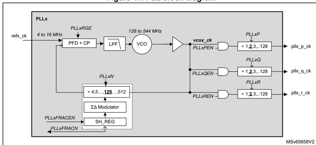
PLLxN loop divider must be programmed to achieve the expected frequency at VCO output. In addition, the VCO output range must be respected.
The PLLx operates in integer mode when PLLxFRACEN is 0, and the PLL is enabled with PLLxON. The fractional mode can be enabled at any time by setting PLL1FRACN to the
required value, and subsequently setting PLLxFRACEN from 0 to 1. The \( \Sigma\Delta \) modulator is designed to minimize the jitter impact while allowing very small step frequency adjustments. To update the fractional value, first set PLLxFRACEN to 0 before updating the PLLxFRACN value, and subsequently set PLLxFRACEN to 1. The old PLLxFRACN value is kept used until the new value is activated by setting PLLxFRACEN from 0 to 1. PLLxFRACN must only be updated by software when PLLxFRACEN is 0.
The PLLs can be enabled by setting PLLxON = 1 in RCC_CR. The PLLxRDY bit indicates that the PLL is ready (meaning locked).
Note: Before enabling the PLLs, make sure that the reference frequency (refx_ck) provided to the PLL is stable. The following PLLx parameters cannot be changed once the PLLx is enabled: PLLxSRC, PLLxN, PLLxRGE, PLLxP, PLLxQ, and PLLxR.
The hardware prevents writing PLL1ON to 0 if the PLL1 is currently used to deliver the system clock.
The following PLL parameters cannot be changed once the PLL is enabled: PLLxN, PLLxRGE, PLLxP, PLLxQ, and PLLxR.
To ensure an optimal behavior of the PLL when one of the post-dividers (PLLxP, PLLxQ, or PLLxR) is not used, the application must clear the enable bit (PLLxPEN, PLLxQEN, PLLxREN), and configure the corresponding post-dividers to their minimum value (PLLxR = 0, PLLxP = 0, or PLLxQ = 0).
If the above rules are not respected, the PLL output frequency is not guaranteed.
Output frequency computation
When the PLL operates in integer mode (SH_REG = 0), the VCO frequency ( \( F_{VCO} \) ) is given by the following formula ( \( x = 1, 2, 3 \) ):
When the PLL operates in fractional mode (SH_REG \( \neq \) 0), the PLLxN divider must be initialized before enabling the PLLs. However, the PLLxFRACN value can be changed on-the-fly without disturbing the PLL output.
This feature can be used either to generate a specific frequency from any crystal value with a good accuracy, or to fine-tune the frequency on-the-fly.
For each PLL, the VCO frequency is given by the following formula:
For both integer and fractional mode, the PLL1 output frequency is given by the following formula:
The PLLs are disabled by hardware:
- • when the system enters Stop or Standby mode
- • when an HSE failure occurs, when HSE or PLL (clocked by HSE) are used as system clock
The fractional information used by the PLL is reset when disabling the PLL.
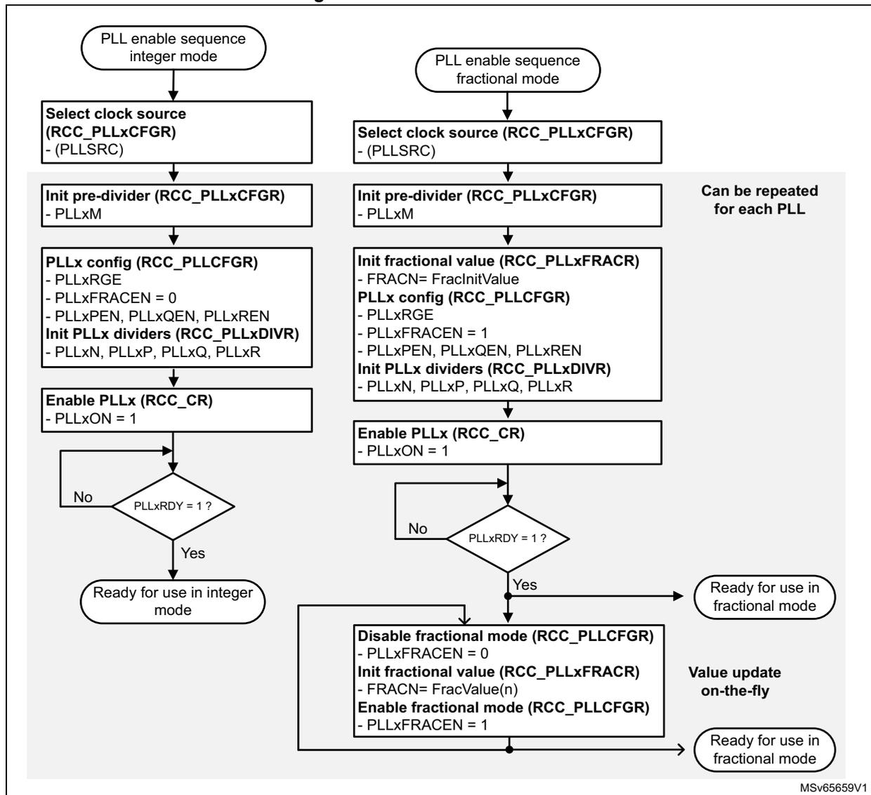
PLL initialization phase
The following PLL initialization sequence in integer and fractional mode is recommended. The PLLx are supposed to be disabled at the start of the initialization sequence:
- 1. Initialize the PLLs registers according to the required frequency.
- – For integer mode, set PLLxFRACEN to 0 in RCC_PLL1CFGR, RCC_PLL2CFGR, and RCC_PLL3CFGR.
- – For fractional mode, set PLLxFRACN to the required initial value (FracInitValue), and then set PLLxFRACEN = 1.
- 2. Once PLLxON = 1, the application must wait until PLLxRDY = 1. As long as PLLxRDY = 0, PLLxFRACEN must not be altered.
- 3. Once PLLxRDY = 1, the PLLx is ready to be used.
- 4. If the application intends to tune the PLLx frequency on-the-fly, then:
- a) PLLxFRACEN must be set to 0 to update the PLLxFRACN value while keeping the PLL running.
- b) Wait at least 3 periods of the PLL reference clock (refx_ck).
- c) A new value can be uploaded into PLLxFRACN (FracValue(n)).
- d) PLLxFRACEN must be set to 1 to activate the new programed value in PLLxFRACN that is taken into account by the PLL.
Figure 42. PLL initialization flow
graph TD
    subgraph IntegerMode [ ]
        direction TB
        I1([PLL enable sequence integer mode]) --> I2[Select clock source
(RCC_PLLxCFGR)
- (PLL_SRC)]
        I2 --> I3[Init pre-divider (RCC_PLLxCFGR)
- PLLxM]
        I3 --> I4[PLLx config (RCC_PLLxCFGR)
- PLLxRGE
- PLLxFRACEN = 0
- PLLxPEN, PLLxQEN, PLLxREN
Init PLLx dividers (RCC_PLLxDIVR)
- PLLxN, PLLxP, PLLxQ, PLLxR]
        I4 --> I5[Enable PLLx (RCC_CR)
- PLLxON = 1]
        I5 --> I6{PLLxRDY = 1?}
        I6 -- No --> I5
        I6 -- Yes --> I7([Ready for use in integer mode])
    end

    subgraph FractionalMode [ ]
        direction TB
        F1([PLL enable sequence fractional mode]) --> F2[Select clock source (RCC_PLLxCFGR)
- (PLL_SRC)]
        F2 --> F3[Init pre-divider (RCC_PLLxCFGR)
- PLLxM]
        F3 --> F4[Init fractional value (RCC_PLLxFRACR)
- FRACN= FracInitValue
PLLx config (RCC_PLLxCFGR)
- PLLxRGE
- PLLxFRACEN = 1
- PLLxPEN, PLLxQEN, PLLxREN
Init PLLx dividers (RCC_PLLxDIVR)
- PLLxN, PLLxP, PLLxQ, PLLxR]
        F4 --> F5[Enable PLLx (RCC_CR)
- PLLxON = 1]
        F5 --> F6{PLLxRDY = 1?}
        F6 -- No --> F5
        F6 -- Yes --> F7([Ready for use in fractional mode])
    end

    I7 --> F8[Disable fractional mode (RCC_PLLxCFGR)
- PLLxFRACEN = 0
Init fractional value (RCC_PLLxFRACR)
- FRACN= FracValue(n)
Enable fractional mode (RCC_PLLxCFGR)
- PLLxFRACEN = 1]
    F7 --> F8
    F8 --> F9([Ready for use in fractional mode])

    style IntegerMode fill:none,stroke:none
    style FractionalMode fill:none,stroke:none
    style F3 fill:none,stroke:none
    style F4 fill:none,stroke:none
    style F8 fill:none,stroke:none
    style F9 fill:none,stroke:none
    style I3 fill:none,stroke:none
    style I4 fill:none,stroke:none
    style I7 fill:none,stroke:none
    style I6 fill:none,stroke:none
    style I5 fill:none,stroke:none
    style I2 fill:none,stroke:none
    style I1 fill:none,stroke:none
    style F3 fill:none,stroke:none
    style F4 fill:none,stroke:none
    style F7 fill:none,stroke:none
    style F6 fill:none,stroke:none
    style F5 fill:none,stroke:none
    style F2 fill:none,stroke:none
    style F1 fill:none,stroke:none
    style F8 fill:none,stroke:none
    style F9 fill:none,stroke:none
The flowchart illustrates the PLL initialization process, starting with two entry points: "PLL enable sequence integer mode" and "PLL enable sequence fractional mode".
Integer Mode Path:
- Select clock source (RCC_PLLxCFGR) - (PLL_SRC)
- Init pre-divider (RCC_PLLxCFGR) - PLLxM
- PLLx config (RCC_PLLxCFGR):
- - PLLxRGE
- - PLLxFRACEN = 0
- - PLLxPEN, PLLxQEN, PLLxREN
- - PLLxN, PLLxP, PLLxQ, PLLxR
- Enable PLLx (RCC_CR) - PLLxON = 1
- Decision: PLLxRDY = 1?
- If No: Loop back to Enable PLLx.
- If Yes: Ready for use in integer mode.
Fractional Mode Path:
- Select clock source (RCC_PLLxCFGR) - (PLL_SRC)
- Init pre-divider (RCC_PLLxCFGR) - PLLxM
- Init fractional value (RCC_PLLxFRACR) - FRACN= FracInitValue
- PLLx config (RCC_PLLxCFGR):
- - PLLxRGE
- - PLLxFRACEN = 1
- - PLLxPEN, PLLxQEN, PLLxREN
- - PLLxN, PLLxP, PLLxQ, PLLxR
- Enable PLLx (RCC_CR) - PLLxON = 1
- Decision: PLLxRDY = 1?
- If No: Loop back to Enable PLLx.
- If Yes: Ready for use in fractional mode.
Value Update on-the-fly:
Both paths lead to a common block for "Value update on-the-fly":
- Disable fractional mode (RCC_PLLxCFGR) - PLLxFRACEN = 0
- Init fractional value (RCC_PLLxFRACR) - FRACN= FracValue(n)
- Enable fractional mode (RCC_PLLxCFGR) - PLLxFRACEN = 1
This sequence results in the system being "Ready for use in fractional mode".
A note indicates that the steps "Init pre-divider", "PLLx config", and "Init PLLx dividers" can be repeated for each PLL.
MSV65659V1
Note: When the PLLxRDY goes to 1, it means that the difference between the PLLx output frequency and the target value is lower than \( \pm 2\% \) .
11.4.7 LSE clock
The LSE crystal is a 32.768 kHz low-speed external crystal or ceramic resonator. It has the advantage of providing a low-power but highly accurate clock source to the real-time clock peripheral (RTC) for clock/calendar or other timing functions.
The LSE crystal is switched on and off using LSEON in RCC_BDCR. If the LSE is used by other peripherals or functions than RTC, TAMP, and LSECSS, the LSESYSEN bit must be also be set in RCC_BDCR (refer to LSE when used by peripherals other than RTC/TAMP, and RCC functions ).
The crystal oscillator driving strength is configured using the LSEDRV[1:0] bits, according to crystal specification, to obtain the best compromise between robustness and short startup
time on one side and low-power-consumption on the other side. The LSE drive must be programmed before enabling the LSE.
LSERDY in RCC_BDCR indicates whether the LSE crystal is stable or not. At startup, the LSE crystal output clock signal is not released until this bit is set by hardware. An interrupt can be generated if enabled in RCC_CIER.
External source (LSE bypass)
In this mode, an external clock source must be provided. This mode is selected by setting LSEBYP and LSEON in RCC_BDCR. The external clock signal (square, sinus, or triangle) with ~50 % duty cycle, must drive the OSC32_IN pin while the OSC32_OUT pin can be used as GPIO (see Figure 39 ).
LSE when used by peripherals other than RTC/TAMP, and RCC functions
By default, when enabled, the LSE is sent only to RTC and TAMP (assuming that RTCSEL = 01).
If the LSE is needed for other peripherals (such as peripheral clock or trigger source), or if the LSE is used by an RCC function (such as LSCO, MCO, MSI PLL mode), the sequence below must be done:
- 1. Set LSEON in RCC_BDCR, and wait for LSERD = 1 in RCC_BDCR.
- 2. Set LSESYSEN = 1 in RCC_BDCR.
- 3. Wait for LSESYSRDY = 1 in RCC_BDCR.
The LSE consumption is increased when LSESYSEN = 1.
11.4.8 LSI clock
The LSI RC acts as a low-power clock source that can be kept running in Stop and Standby modes for the independent watchdog (IWDG) and RTC. The clock frequency is either 32 kHz or 250 Hz depending on LSIPREDIV in RCC_BDCR. Setting LSIPREDIV allows a lower consumption (refer to the electrical characteristics section of the datasheet for more details).
When the IWDG is enabled or when the RTC or TAMP is clocked by the LSI, LSIPREDIV cannot be changed anymore.
The LSI RC can be switched on and off using LSION in RCC_BDCR.
LSIRDY in RCC_BDCR indicates if the LSI oscillator is stable or not. At startup, the clock is not released until this bit is set by hardware. An interrupt can be generated if enabled in RCC_CIER.
11.4.9 System clock (SYSCLK) selection
Four different clock sources can be used to drive the system clock (SYSCLK):
- • MSIS oscillator
- • HSI16 oscillator
- • HSE oscillator
- • PLL
The system clock maximum frequency is 160 MHz. After a system reset, the MSIS oscillator, at 4 MHz, is selected as system clock. When a clock source is used directly or through the PLL as a system clock, it is not possible to stop it.
A switch from one clock source to another occurs only if the target clock source is ready (clock stable after startup delay or PLL locked). If a clock source that is not yet ready is selected, the switch occurs when the clock source becomes ready. Status bits in RCC_CR indicate which clocks are ready and which clock is currently used as a system clock.
The table below gives the different bus frequencies depending on the product voltage range.
Table 114. Bus maximum frequency
| Product voltage range | AHB1/AHB2/AHB3/APB1/APB2/APB3 |
|---|---|
| Range 1 | 160 MHz |
| Range 2 | 110 MHz |
| Range 3 | 55 MHz |
| Range 4 | 25 MHz |
11.4.10 Clock source frequency versus voltage scaling
The table below gives the different clock source frequencies depending on the product voltage range.
Table 115. Clock source maximum frequency
| Voltage range | Clock frequency | |||||
|---|---|---|---|---|---|---|
| MSIS, MSIK | HSI16 | HSI48 | SHS1 | HSE | PLL outputs (VCO min to max) | |
| Range 1 | All ranges | Allowed | Allowed | Allowed | 50 MHz | 208 MHz (1) (128 to 544 MHz) |
| Range 2 | All ranges | Allowed | Allowed | Allowed | 50 MHz | 110 MHz (128 to 544 MHz) |
| Range 3 | All ranges | Allowed | Allowed | Allowed | 50 MHz | 55 MHz (128 to 330 MHz) |
| Range 4 | Up to 24 MHz range | Allowed | Allowed (divided by 2) | Allowed (divided by 2) | 25 MHz | Not allowed |
- 1. The maximum frequency depends on peripherals connected to PLL outputs.
11.4.11 Clock security system (CSS)
The CSS can be activated by software. In this case, the clock detector is enabled after the HSE oscillator wake-up time, and disabled when this oscillator is stopped.
If a failure is detected on the HSE clock, the HSE oscillator is automatically disabled. A clock failure event is sent to some timers break input and an interrupt is generated to inform the software about the failure (clock security system interrupt CSSI). This allows the MCU to perform rescue operations. The CSSI is linked to the Cortex-M33 NMI (nonmaskable interrupt) exception vector.
Note: Once the CSS is enabled and if the HSE clock fails, the CSSI occurs and an NMI is automatically generated. The NMI is executed indefinitely unless CSSI bit is cleared. As a consequence, in the NMI ISR, the user must clear the CSSI by setting CSSC in RCC_CICR.
If the HSE oscillator is used directly or indirectly as the system clock (indirectly means: it is used as PLL input clock and the PLL clock is used as system clock), a detected failure causes a switch of the system clock to the MSIS or the HSI16 oscillator depending on STOPWUCK configuration in RCC_CR, and the disabling of the HSE oscillator. If the HSE clock (divided or not) is the clock entry of the PLL used as system clock when the failure occurs, the PLL is disabled too.
11.4.12 Clock security system on LSE
A clock security system on LSE can be activated by software writing LSECSSON in RCC_BDCR. This bit can be disabled only by a hardware reset or RTC software reset, or after a failure detection on LSE. LSECSSON must be written after LSE is enabled (LSEON enabled) and ready (LSERDY set by hardware), and after the RTC clock has been selected by RTCSEL.
The CSS on LSE works in all modes, including V BAT mode. It works also under system reset (excluding power-on reset).
The CSS on LSE detects when the LSE disappears or in case of over frequency. In addition, the glitches on LSE can be filtered by setting LSEGFON. LSEGFON must be written when the LSE is disabled (LSEON = 0 and LSERDY = 0).
If a failure is detected on the external 32 kHz oscillator, the LSE clock is no longer supplied to the RTC, but no hardware action is made to the registers. If the MSI was in PLL-mode, this mode is disabled.
The CSS on LSE detection event is connected to the internal tamper 3 of the TAMP:
- • On STM32U575/585 rev. X devices, the internal tamper 3 must be enabled (ITAMP3E = 1 in TAMP_CR1) and the associated interrupt enabled (ITAMP3IE in TAMP_IER) in order to wake up from the low-power modes. This erases also the TAMP backup registers and backup SRAM unless ITAMP3NOER = 1 in TAMP_CR3 (see Section 64: Tamper and backup registers (TAMP) for more details).
- • On all other STM32U575/585 revisions, and the other STM32U5 devices, the CSS on LSE detection event is also connected to an EXTI line, allowing to generate an event or interrupt supporting wake-up from Stop 0, Stop 1, or Stop 2 mode, without requiring to enable tamper detection (see Table 118: Interrupt sources and control and Table 189: EXTI line connections ).
In case of CSS on LSE detection event (LSECSSD = 1 in RCC_BDCR), the software must then disable the LSECSSON bit, stop the defective 32 kHz oscillator (disabling LSEON), and change the RTC clock source (no clock or LSI or HSE, with RTCSEL), or take any required action to secure the application.
Refer to datasheet for CSS on LSE electrical characteristics.
11.4.13 ADC and DAC clocks
The ADC and DAC kernel clock source is selected thanks to ADCDACSEL[2:0] in RCC_CCIPR3. The ADC clock ratio must be around 50 %. For this reason, the AHB clock, when selected as ADC clock, must not be divided with HPRE prescaler. If pll2_r_ck is selected as ADC clock, the PLL2R division factor must be even (division by 2 or 4 for example).
If the application requires that the ADC or DAC is precisely triggered by a TIMx timer without any uncertainty, the HCLK must be selected as ADC and DAC kernel clock source.
The other clock sources are asynchronous to TIMx timers therefore an uncertainty of the trigger instant is added by the resynchronization between the two clock domains. LPTIMx timers are also asynchronous.
The DAC requires an additional low-power clock (LSI or LSE) to operate in sample and hold mode, available in Stop mode. This clock is selected with DAC1SEL in the RCC_CCIPR3.
11.4.14 RTC and TAMP clock
The RTCCLK clock source is used by RTC and TAMP, and can be either the HSE / 32, LSE, or LSI clock. It is selected by programming RTCSEL[1:0] in RCC_BDCR. This selection cannot be modified without resetting the backup domain. The system must always be configured so as to get a PCLK frequency greater than or equal to the RTCCLK frequency for a proper operation of the RTC. The TAMP does not require any kernel clock if only backup registers are used, with tamper in edge detection mode. All other tamper detection modes require a kernel clock (refer to Section 64: Tamper and backup registers (TAMP) for more details).
LSE and LSI clocks are in the backup domain, whereas the HSE clock is not. Consequently:
- • If LSE or LSI is selected as RTC and TAMP clock, these peripherals continue to work even if the \( V_{DD} \) supply is switched off, provided the \( V_{BAT} \) supply is maintained.
- • If the HSE clock divided by a prescaler is used as the RTC or TAMP clock, the RTC state is not guaranteed if the \( V_{DD} \) supply is powered off, or if the internal voltage regulator is powered off (removing power from the core domain). Depending on the TAMP configuration, this one can remain functional if used in a mode that does not need any kernel clock.
When the RTC and TAMP clock is LSE or LSI, the RTC remains clocked and functional under system reset.
If the LSE is needed only for the RTC or TAMP, LSESYSEN must be kept at reset value to get the lowest consumption.
11.4.15 Timer clock
The timer clock frequencies are automatically defined by hardware.
There are two cases:
- • If the APB prescaler equals 1, the timer clock frequencies are set to the APB domain frequency.
- • Otherwise, they are set to twice ( \( \times 2 \) ) the APB domain frequency.
11.4.16 Watchdog clock
If the independent watchdog (IWDG) is started by either hardware option or software access, the LSI oscillator is forced on and cannot be disabled. After the LSI oscillator temporization, the LSI 32 kHz clock is provided to the IWDG.
11.4.17 OCTOSPI clock
The OCTOSPIx kernel clock, selected by OCTOSPIxSEL[1:0], can be up to 200 MHz when pll1_q_ck or pll2_q_ck are used.
11.4.18 HSPI1 clock
The HSPI1 kernel clock, selected by HSPI1SEL[1:0], can be up to 200 MHz when pll1_q_ck, pll2_q_ck or pll3_r_ck are used.
11.4.19 OTG_HS clock
The OTG_HS kernel clock is generated by the OTG_HS PHY. This PHY can accept only frequencies of following list (16, 19.2, 20, 24, 26 or 32 MHz), with an accuracy of \( \pm 400 \) ppm. Those frequencies can be achieved using either HSE, HSE/2, PLL1_P or PLL1_P/2, and selected by the OTGHSSSEL[1:0] multiplexer. Refer to the OTGHSSSEL description concerning some limitations that apply when using the PLL as its input.
11.4.20 DSI clock
The DSI interface clock can be derived from the internal DSI PHY PLL or by the pll3_p_ck clocks, selected by DSISEL multiplexer.
11.4.21 LTDC clock
The LTDC interface clock can be derived from the pll2_r_ck or pll3_r_ck clocks, selected by LTDCSEL multiplexer.
11.4.22 Clock-out capability
- • MCO
The microcontroller clock output (MCO) capability allows the clock to be output onto the external MCO pin. One of the following clock signals can be selected as MCO clock.
- – LSI
- – LSE
- – SYSCLK
- – HSI16
- – HSI48
- – HSE
- – PLLCLK
- – MSIS
- – MSIK
This output remains available in Stop0, Stop1 and Stop2. In Stop modes, selection of available clock signals may be limited.
The selection is controlled by MCOSEL[3:0] in RCC_CR. The selected clock can be divided with MCOPRE[2:0] in RCC_CR.
- • LSCO
Another output (LSCO) allows one of the low-speed clocks below to be output onto the external LSCO pin:
- – LSI
- – LSE
This output remains available in all Stop modes, Standby, and Shutdown modes.
This output is not available in \( V_{BAT} \) mode. The selection is controlled by LSCOSEL bit and enabled with LSCOEN in RCC_BDCR.
The MCO clock output requires the corresponding alternate function selected on MCO pin.
11.4.23 Internal/external clock measurement with TIM15/TIM16/TIM17/LPTIM1/LPTIM2
The frequency of all on-board clock sources can be indirectly measured by means of the TIM15, TIM16, or TIM17 channel 1 input capture, and LPTIM1 or LPTIM2 channel 2 input capture.
HSI16 and MSI calibration using LSE
The primary purpose of connecting the LSE to the channel 1 input capture of TIM15, TIM16, and TIM17, and to the channel 2 input capture of LPTIM1, is to be able to precisely measure the HSI16 and MSI system clocks (for this, either HSI16 or MSIS must be used as system clock source). The number of HSI16 (MSIS respectively) clock counts between consecutive edges of the LSE signal provides a measure of the internal clock period. Taking advantage of the high precision of LSE crystals (typically a few tens of ppms), the internal clock frequency can be determined with the same resolution, and the source can be trimmed to compensate the manufacturing, process, temperature and/or voltage related frequency deviations.
The four oscillators of MSI and HSI16 oscillator have dedicated user-accessible calibration bits for this purpose.
The basic concept consists in providing a relative measurement (such as HSI16/LSE ratio). The precision is therefore closely related to the ratio between the two clock sources. The higher the ratio is, the better the measurement is.
Note: When the LSE is available, the MSI can be automatically trimmed by LSE using PLL-mode.
HSI16 and MSI calibration using HSE
If the HSE is available, it can be used as system clock, and the timer input capture must be connected either to MSI (divided by 1024 or by 4) or to HSI/256. TIM16 and TIM17 channel 1 input capture, as well and the LPTIM2 input capture 2, are connected to the divided oscillator only when TIMICSEL[2:0] \( \neq \) 0 in RCC_CCIPR1.
Considering that the timer counter is 16-bit, and that the ratio between HSE and the input capture signal must be the highest possible, a division by 1024 must be selected when MSIRC0, MSIRC1, or MSIRC2 is measured, and a division by 4 when MSIRC4 is measured.
LSI calibration
The calibration of the LSI follows the same principle, but changing the reference clock. The LSI clock must be connected to the channel 1 input capture of the TIM16 or TIM17, or to the channel 2 input capture of the LPTIM1. Then defining the HSE as system clock source, the number of its clock counts between consecutive edges of the LSI signal, provides a measure of the internal low-speed clock period.
The basic concept consists in providing a relative measurement (such as HSE/LSI ratio). The precision is therefore closely related to the ratio between the two clock sources. The higher the ratio is, the better the measurement is.
11.4.24 Peripherals clock gating and autonomous mode
Peripherals clock gating in Run mode
Each peripheral clock can be enabled by the corresponding EN bit in RCC_AHBxENR and RCC_APBxENR registers.
When the peripheral clock is not active, read or write accesses to the peripheral registers are not supported.
The enable bit has a synchronization mechanism to create a glitch-free clock for the peripheral. After the enable bit is set, there the clock is active after 2 cycles of the peripheral bus clock.
Caution: Just after enabling the clock for a peripheral, the software must wait for these two clock cycles before accessing the peripheral registers.
Peripherals clock gating in Sleep and Stop modes
When a peripheral is enabled, its clock can be automatically gated off when the device is in Sleep mode, by clearing the peripheral SMEN bit in RCC_AHBxSMENR and RCC_APBxSMENR. Both EN and SMEN of the peripheral must be set to keep the clock on in Sleep mode.
The SMEN bit of the peripheral is also used to allow peripheral clocking in Stop 0 and Stop 1 modes, upon peripheral request.
When the clock is requested by a peripheral, this clock is distributed to all enabled peripherals. Therefore, the SMEN bit must be cleared before entering Stop mode, if the peripheral is not used in Stop mode.
Caution: The SMEN bit of the peripheral must be set to allow the generation of an interrupt capable to wake up the device from Stop mode. This is not necessary when the peripheral wake-up interrupt is generated through the EXTI.
Peripherals clock gating and autonomous mode in Stop 0/1/2 modes
Some peripherals support autonomous mode (refer to Table 116 ). These peripherals are able to generate a kernel clock request and a AHB/APB bus clock request when they need, in order to operate and update their status register even in Stop mode. Depending on the peripheral configuration, either a DMA request or an interrupt can be associated to the peripheral event.
Upon an AHB or APB bus clock request from an autonomous peripheral, either MSI or HSI16 oscillator is woken up, depending on the oscillator selected by STOPWUCK in RCC_CFGR1.
If the autonomous peripheral is configured with DMA requests enabled, a data transfer is performed thanks to the AHB/APB clock. The bus clocks as well as the oscillator (HSI16 or MSI) are automatically switched off as soon as the transfer is finished, if no other peripheral requests it. The device automatically goes back in Stop mode.
If the autonomous peripheral is configured with interrupt enabled, the interrupt wakes up the device into Run mode.
The autonomous peripherals mapped on AHB3 or APB3 belong to the SmartRun domain and are autonomous in Stop 0, Stop 1, and Stop 2 with the LPDMA1 and SRAM4.
The autonomous peripherals mapped on AHB1, AHB2, APB1, and APB2, belong to the CPU domain, and are autonomous in Stop 0 and Stop 1 mode, only with GPDMA1 and SRAM1/2/3/4/5/6.
The table below shows the list of peripherals with autonomous mode capability.
Table 116. Autonomous peripherals
| Domain | Peripheral | Autonomous in Stop 0, 1 modes | Autonomous in Stop 2 mode | Associated DMA | Associated SRAM |
|---|---|---|---|---|---|
| CPU domain (CD) | U(S)ARTx (x = 1 to 6) | Yes (1) | No | GPDMA1 | SRAM1 SRAM2 SRAM3 SRAM4 (2) SRAM5 SRAM6 |
| SPIx (x = 1,2) | |||||
| I2Cx (x = 1,2,4,5,6) | |||||
| LPTIM2 | |||||
| MDF1 | |||||
| GPDMA1 | - | ||||
| SmartRun domain (SRD) | LPUART1 | Yes (3) | Yes (3) | LPDMA1 | SRAM4 |
| SPI3 | |||||
| I2C3 | |||||
| LPTIMx (x = 1,3,4) | |||||
| ADF1 | |||||
| DAC1 | |||||
| ADC4 | |||||
| LPDMA1 | - |
1. Enabled if both xxEN and xxSMEN bits of the peripheral are set (xx = instance name)
2. SRAM4 belongs to SmartRun domain (SRD) but can be addressed by GPDMA 1 in Stop 0 and Stop 1 modes.
3. Enabled if all xxEN, xxSMEN, and xxAMEN bits of the peripheral are set (xx = instance name)
For peripherals in the CPU domain, the autonomous mode is enabled in Stop 0 and Stop 1 modes if both xxEN and xxSMEN bits of the peripheral are set.
For peripherals in SmartRun domain, the autonomous mode is enabled in Stop 0, Stop 1, and Stop 2 modes if both xxEN and xxSMEN bits of the peripheral are set, plus xxAMEN bit of the peripheral in RCC_SRDRAMR.
If an autonomous peripheral requests its kernel clock in Stop 0, Stop 1, or Stop 2 mode, the internal oscillator (HSI16 or MSI) is woken up if it was off, and the kernel clock is propagated only to the peripheral requesting it. When the peripheral releases its kernel clock request, the HSI16 or MSI is switched off if no other peripheral requests it.
If an autonomous peripheral belonging to CPU domain requests its bus clock (AHB1, AHB2, APB1, or APB2 clock) in Stop 0 or Stop 1 mode, the internal oscillator (HSI16 or MSI depending on STOPWUCK value in RCC_CFGR1) is woken up if it was off, and the system clock is propagated to all peripherals configured with both xxEN = xxSMEN = 1.
If an autonomous peripheral belonging to SmartRun domain requests its bus clock (AHB3 or APB3 clock) in Stop 0, Stop 1, or Stop 2 mode, the internal oscillator (HSI16 or MSI depending on STOPWUCK value in RCC_CFGR1) is woken up if it was off, and
HCLK3/PCLK3 clocks are propagated to all peripherals of the SmartRun domain configured with xxEN = xxSMEN = xxAMEN = 1.
Caution: The AMEN bit of the peripheral must be set to allow the generation of an interrupt capable to wake up the device from Stop mode. This is not necessary when the peripheral wake-up interrupt is generated through the EXTI.
Note: MSI or HSI16 can be forced to remain on in Stop 0, Stop 1, or Stop 2 mode, by configuring MSIKERON or HSIKERON in RCC_CR. In this case, the oscillator is propagated only to the kernel clock of the enabled autonomous peripherals with this oscillator selected as kernel clock. This allows the peripheral baudrate or conversion rate increase, as there is no need to wait for the oscillator wake-up time when the peripheral requests its kernel clock.
The LSE or LSI selected as peripheral kernel clock remains always on in Stop modes.
AHB3 and APB3 clocks can be forced to remain on by setting SRDRUN in PWR_CR2. This allows the LPDMA1 latency to be improved as there is no need to wait for the oscillator wake-up time when the peripheral requests its bus clock.
11.5 RCC security and privilege functional description
11.5.1 RCC TrustZone security protection modes
When the TrustZone security is activated by TZEN option bit in FLASH_OPTR, the RCC is able to secure RCC configuration and status bits from being modified by nonsecure accesses.
This is configured through RCC_SECCFGR to prevent nonsecure access to read or modify the following features:
- • HSE, HSE-CSS, HSI, MSI, LSI, LSE, LSE-CSS, LSCO, HSI48 configuration and status bits
- • PLL1, PLL2, PLL3, AHB, and APB prescaler configuration and status bits
- • system clock (SYSCLK) and ICLK source clock selection and status bits
- • MCO clock output configuration, and STOPWUCK and STOPKERWUCK bit
- • Remove reset flag RMVF configuration
If SPRIV = 1 in RCC_PRIVCFGR, the RCC_SECCFGR register can be written only by secure and privileged access. If SPRIV = 0 in RCC_PRIVCFGR, RCC_SECCFGR can be written only by secure access, privileged or unprivileged.
RCC_SECCFGR can be read by secure, nonsecure, privileged and unprivileged access.
When a peripheral is configured as secure, its related clock, reset, clock source selection and clock enable during low-power modes control bits, are also secure in RCC_AHBxENR, RCC_APBxENR, RCC_AHBxSMEN, RCC_APBxSMEN, RCC_SRDAMEN, RCC_CCIPR1, RCC_CCIPR2, RCC_CCIPR3, and RCC_BDCR registers.
The SHSI configuration and status bits are secured when the SAES is configured as secure.
BDRST in RCC_BDCR is secure when at least one function is secure in RTC or TAMP.
A peripheral is secure when:
- • For securable peripherals by TZSC (TrustZone security controller), the SEC security bit corresponding to this peripheral is set in GTZC TZSC secure configuration registers.
- • For TrustZone-aware peripherals, a security feature of this peripheral is enabled through its dedicated bits.
Table 117 summarizes the RCC secured bits following the security configuration bit in RCC_SECCFGR register.
When one security configuration bit is set, some configuration and status bits are secured. The RCC registers may contain secure and nonsecure bits:
- • Secured bits: read and write operations are only allowed by a secure access. Nonsecure read returns 0 and write accesses are ignored. No illegal access event is generated.
- • Nonsecure bits: no restriction. Read and write operations are allowed by both secure and nonsecure accesses.
- • A nonsecure write access to RCC_SECCFGR is ignored and generates an illegal access event. An illegal access interrupt is generated if the RCC illegal access interrupt is enabled in the GTZC TZIC registers. RCC_SECCFGR can be read by secure or nonsecure access.
When the TrustZone security is disabled (TZEN = 0 in FLASH_OPTR), all registers are nonsecure. RCC_SECCFGR write accesses are ignored.
Table 117. RCC security configuration summary
| Configuration bit in RCC_SECCFGR | Secured bits | Corresponding register |
|---|---|---|
| HSISEC | HSION, HSIKERON, HSIRDY | RCC_CR |
| HSICAL[7:0], HSITRIM[6:0] | RCC_ICSCR3 | |
| HSIRDYIE | RCC_CIER | |
| HSIRDYIF | RCC_CIFR | |
| HSIRDYC | RCC_CICR | |
| HSESEC | HSEON, HSERDY, HSEBYP, CSSON, HSEEXT | RCC_CR |
| HSERDYIE | RCC_CIER | |
| HSERDYIF, CSSF | RCC_CIFR | |
| HSERDYC, CSSC | RCC_CICR | |
| MSISEC | MSISON, MSIKERON, MSISRDY, MSIPLLEN, MSIKON, MSIKRDY, MSIPLLSEL, MSIPLLFAST | RCC_CR |
| MISIRANGE[3:0], MISIKRANGE[3:0], MSIRGSEL, MSIBIAS, MSICAL0[4:0], MSICAL1[4:0], MSICAL2[4:0], MSICAL3[4:0] | RCC_ICSCR1 | |
| MSITRIM0[4:0], MSITRIM1[4:0], MSITRIM2[4:0], MSITRIM3[4:0] | RCC_ICSCR2 | |
| MSISRDYIE, MSIKRDYIE | RCC_CIER | |
| MSISRDYIF, MSIKRDYIF | RCC_CIFR | |
| MSISRDYIC, MSIKRDYIC | RCC_CICR | |
| MSISSRANGE[3:0], MSIKSRANGE[3:0] | RCC_CSR |
Table 117. RCC security configuration summary (continued)
| Configuration bit in RCC_SECCFGR | Secured bits | Corresponding register |
|---|---|---|
| LSISEC | LSION, LSIRDY, LSIPREDIV, LSCOSEL, LSCOEN | RCC_BDCR |
| LSIRDYIE | RCC_CIER | |
| LSIRDYIF | RCC_CIFR | |
| LSIRDYC | RCC_CICR | |
| LSESEC | LSECSSON, LSECSSD, LSEDRV[1:0], LSEBYP, LSERDY, LSEON, LSEGON, LSESYSRDY, LSESYSEN, LSCOSEL, LSCOEN | RCC_BDCR |
| LSERDYIE | RCC_CIER | |
| LSERDYF | RCC_CIFR | |
| LSERDYC | RCC_CICR | |
| SYSCLKSEC | SW[1:0], SWS[1:0], STOPWUCK, STOPKERWUCK, MCOSEL[3:0], MCOPRE[2:0] | RCC_CFGR1 |
| SYSTICKSEL[1:0] | RCC_CCIPR1 | |
| VOS[1:0] | PWR_VOSR | |
| PRESCSEC | HPRE[3:0], PPRE1[2:0], PPRE2[2:0] | RCC_CFGR2 |
| PPRE3[2:0] | RCC_CFGR3 | |
| PLL1SEC | PLL1SRC[1:0], PLL1RGE[1:0], PLL1FRACEN, PLL1M[3:0], PLL1MBOOST[3:0], PLL1PEN, PLL1QEN, PLL1REN | RCC_PLL1CFGR |
| PLL1N[8:0], PLL1P[6:0], PLL1Q[6:0], PLL1R[6:0] | RCC_PLL1DIVR | |
| PLL1FRACN[12:0] | RCC_PLL1FRACR | |
| PLL1RDY, PLL1ON | RCC_CR | |
| PLL1RDYIE | RCC_CIER | |
| PLL1RDYF | RCC_CIFR | |
| PLL1RDYC | RCC_CICR | |
| PLL2SEC | PLL2SRC[1:0], PLL2RGE[1:0], PLL2FRACEN, PLL2M[3:0], PLL2PEN, PLL2QEN, PLL2REN | RCC_PLL2CFGR |
| PLL2N[8:0], PLL2P[6:0], PLL2Q[6:0], PLL2R[6:0] | RCC_PLL2DIVR | |
| PLL2FRACN[12:0] | RCC_PLL2FRACR | |
| PLL2RDY, PLL2ON | RCC_CR | |
| PLL2RDYIE | RCC_CIER | |
| PLL2RDYF | RCC_CIFR | |
| PLL2RDYC | RCC_CICR |
Table 117. RCC security configuration summary (continued)
| Configuration bit in RCC_SECCFGR | Secured bits | Corresponding register |
|---|---|---|
| PLL3SEC | PLL3SRC[1:0], PLL3RGE[1:0], PLL3FRACEN, PLL3M[3:0], PLL3PEN, PLL3QEN, PLL3REN | RCC_PLL3CFGR |
| PLL3N[8:0], PLL3P[6:0], PLL3Q[6:0], PLL3R[6:0] | RCC_PLL3DIVR | |
| PLL3FRACN[12:0] | RCC_PLL3FRACR | |
| PLL3RDY, PLL3ON | RCC_CR | |
| PLL3RDYIE | RCC_CIER | |
| PLL3RDYF | RCC_CIFR | |
| PLL3RDYC | RCC_CICR | |
| HSI48SEC (1) | HSI48ON, HSI48RDY | RCC_CR |
| HSI48CAL[8:0] | RCC_CRRCR | |
| HSI48RDYE | RCC_CIER | |
| HSI48RDYF | RCC_CIFR | |
| HSI48RDYC | RCC_CICR | |
| ICLKSEL | ICLKSEL[1:0] | RCC_CCIPR1 |
| RMVFSEC | RMVF | RCC_CSR |
1. TRIM field of the HSI48 is located in CRS peripheral. Be sure to secure it using CRSSEC bit in GTZC1 TZSC secure configuration register 1.
11.5.2 RCC privilege protection modes
By default, after reset, all RCC registers can be read or written with both privileged and unprivileged access, except RCC_PRIVCFGR that can be written with privileged access only. RCC_PRIVCFGR can be read by secure and nonsecure, privileged and unprivileged access.
SPRIV in RCC_PRIVCFGR can be written with secure privileged access only. This bit configures the privileged access of all RCC secure functions (as defined by RCC_SECCFGR), or by the GTZC for securable peripherals, or by the peripheral itself in case of TrustZone-aware peripherals).
When SPRIV = 1 in RCC_PRIVCFGR:
- • Writing the RCC secure bits is possible only with privileged access, including RCC_SECCFGR.
- • The RCC secure bits can be read only with privileged access, except RCC_SECCFGR and RCC_PRIVCFGR that can be read by privileged or unprivileged access.
- • An unprivileged access to a privileged RCC bit or register is discarded: the bits are read as zero and the write to these bits is ignored (RAZ/WI).
NSPRIV in RCC_PRIVCFGR can be written with privileged access only, secure or nonsecure functions (as defined by RCC_SECCFGR, or by the GTZC for securable peripherals, or by the peripheral itself in case of TrustZone-aware peripherals).
When NSPRIV = 1 in RCC_PRIVCFGGR:
- • Writing the RCC nonsecure bits is possible only with privileged access.
- • The RCC nonsecure bits can be read only with privileged access except RCC_PRIVCFGGR that can be read by privileged or unprivileged access.
- • An unprivileged access to a privileged RCC bit or register is discarded: the bits are read as zero and the write to these bits is ignored (RAZ/WI).
11.6 RCC low-power modes
- • AHB and APB peripheral clocks, including DMA clock, can be disabled by software.
- • Sleep mode stops the CPU clock. The memory interface clocks (flash memory, caches, and all SRAM interfaces) can be stopped by software during Sleep mode. The AHB to APB bridge clocks are disabled by hardware during Sleep mode when all the clocks of the peripherals connected to them are disabled.
- • Stop modes (Stop 0, Stop 1, Stop 2, Stop 3) stop all the clocks in the core domain and disable the PLLs, HSI16, HSI48, SHSI, MSI, and HSE oscillators. However, HSI16 or MSI can be switched ON if the peripheral requests it for autonomous mode purpose, or to generate a wake-up interrupt (see Section 11.4.24 for more details). LSI and LSE remain active in Stop modes.
- • Standby and Shutdown modes stop all the clocks in the core domain and disable the PLLs, HSI16, HSI48, SHSI, MSI, and HSE oscillators.
The CPU deep-sleep mode can be overridden for debugging by setting the DBG_STOP or DBG_STANDBY bit in the DBGMCU_CR register.
When exiting Stop modes (Stop 0, Stop 1, Stop 2, or Stop 3), the system clock is either MSIS or HSI16, depending on STOPWUCK in RCC_CFGR1. The frequency (range and user trim) of MSIS and MSIK oscillators is the one configured before entering Stop mode, except if above 24 MHz. In this case, the MSIS or MSIK range is the 24 MHz range. The user trim of HSI16 is kept. If MSI is in PLL-mode before entering Stop mode with MSIPLLFAST = 0, the PLL-mode stabilization time must be waited for after wake-up even if the LSE was kept on during Stop mode. The PLL-mode accuracy is kept after wake-up from Stop 0, Stop 1, or Stop 2 mode without stabilization time if MSIPLLFAST = 1. MSIPLLFAST bit has no effect when exiting Stop 3 mode.
The other internal oscillator can be automatically woken up in addition to the one used by the system clock, in order to avoid waiting for the other oscillator wake-up time when the device is back in Run mode. This is done thanks to STOPKERWUCK in RCC_CFGR1.
When leaving the Standby and Shutdown modes, the system clock is MSIS. The MSIS and MSIK frequency at wake-up from Standby mode is configured with MSISSRANGE and MSIKSRANGE in RCC_CSR, from 1 to 4 MHz. The MSI frequency at wake-up from Shutdown mode is 4 MHz. The user trim is lost.
If a flash memory programming operation is ongoing, a Stop, Standby, or Shutdown mode entry is delayed until the flash memory interface access is finished. If an access to the APB domain is ongoing, a Stop, Standby, or Shutdown mode entry is delayed until the APB access is finished. If an autonomous peripheral generates a system clock request, a Stop, Standby, or Shutdown mode entry is delayed until the system clock request is released.
11.7 RCC interrupts
The table below summarizes the interrupt sources and the way to control them.
Table 118. Interrupt sources and control
| Interrupt vector | Interrupt event flag | Description | Enable control bit | Interrupt clear method | Exit Sleep mode | Exit Stop, Standby, Shutdown modes |
|---|---|---|---|---|---|---|
| RCC | LSIRDYF | LSI ready | LSIRDYIE and LSISEC = 0 | Set LSIRDYC to 1 | Yes | No |
| LSERDYF | LSE ready | LSERDYIE and LSESEC = 0 | Set LSERDYC to 1 | Yes | No | |
| HSIDRYF | HSI ready | HSIDRYIE and HSISEC = 0 | Set HSIRDYC to 1 | Yes | No | |
| HSERDYF | HSE ready | HSERDYIE and HSESEC = 0 | Set HSERDYC to 1 | Yes | No | |
| MSISRDYF | MSIS ready | MSISRDYIE and MSISEC = 0 | Set MSISRDYC to 1 | Yes | No | |
| MSIKRDYF | MSIK ready | MSIKRDYIE and MSISEC = 0 | Set MSIKRDYC to 1 | Yes | No | |
| SHSIRDYF | SHSI ready | SHSIRDYIE and SAESSEC = 0 (in GTZC) | Set SHSIRDYC to 1 | Yes | No | |
| HSI48RDYF | HSI48 ready | HSI48RDYIE and HSI48SEC = 0 | Set HSI48RDYC to 1 | Yes | No | |
| PLL1RDYF | PLL1 ready | PLL1RDYIE and PLL1SEC = 0 | Set PLL1RDYC to 1 | Yes | No | |
| PLL2RDYF | PLL2 ready | PLL2RDYIE and PLL2SEC = 0 | Set PLL2RDYC to 1 | Yes | No | |
| PLL3RDYF | PLL3 ready | PLL3RDYIE and PLL3SEC = 0 | Set PLL3DYC to 1 | Yes | No | |
| RCC_S (1) | LSIRDYF | LSI ready | LSIRDYIE and LSISEC = 1 | Set LSIRDYC to 1 | Yes | No |
| LSERDYF | LSE ready | LSERDYIE and LSESEC = 1 | Set LSERDYC to 1 | Yes | No | |
| HSIDRYF | HSI ready | HSIDRYIE and HSISEC = 1 | Set HSIRDYC to 1 | Yes | No | |
| HSERDYF | HSE ready | HSERDYIE and HSESEC = 1 | Set HSERDYC to 1 | Yes | No | |
| MSISRDYF | MSIS ready | MSISRDYIE and MSISEC = 1 | Set MSISRDYC to 1 | Yes | No | |
| MSIKRDYF | MSIK ready | MSIKRDYIE and MSISEC = 1 | Set MSIKRDYC to 1 | Yes | No |
Table 118. Interrupt sources and control (continued)
| Interrupt vector | Interrupt event flag | Description | Enable control bit | Interrupt clear method | Exit Sleep mode | Exit Stop, Standby, Shutdown modes |
|---|---|---|---|---|---|---|
| RCC_S (1) | SHSIRDYF | SHSI ready | SHSIRDYIE and SAESSEC (2) = 1 | Set SHSIRDYC to 1 | Yes | No |
| HSI48RDYF | HSI48 ready | HSI48RDYIE and HSI48SEC = 1 | Set HSI48RDYC to 1 | Yes | No | |
| PLL1RDYF | PLL1 ready | PLL1RDYIE and PLL1SEC = 1 | Set PLL1RDYC to 1 | Yes | No | |
| PLL2RDYF | PLL2 ready | PLL2RDYIE and PLL2SEC = 1 | Set PLL2RDYC to 1 | Yes | No | |
| PLL3RDYF | PLL3 ready | PLL3RDYIE and PLL3SEC = 1 | Set PLL3RDYC to 1 | Yes | No | |
| TAMP | ITAMP3F (3) | LSE CSS failure | LSECSSON and ITAMP3E (3) and ITAMP3IE (3) | Set CITAMP3F (3) to 1 | Yes | Yes |
| NMI | CSSF | HSE CSS failure | _(4) | Set CSSC to 1 | Yes | No |
| LSECSS (5) | Through EXTI | LSE CSS failure | Through EXTI | Through EXTI | Yes | Yes (6) /No |
| MSI_PLL_UNLOCK (5) | Through EXTI | MSI PLL-mode unlock (7) | Through EXTI | Through EXTI | Yes | Yes (6) /No |
1. The RCC secure interrupt vector is used only when TrustZone is enabled.
2. The SAESSEC bit is in the GTZC peripheral.
3. The LSE CSS failure event (LSECSSD) is connected to TAMP internal tamper 3. In order to get the interrupt associated to this event, the internal tamper 3 must be enabled, and the internal tamper 3 interrupt must be enabled. The ITAMP3F, ITAMP3E, ITAMP3IE, and CITAMP3F bits are in the TAMP peripheral. Consequently, the LSE CSS tamper interrupt erases or blocks the device secrets as described in Table 644: TAMP interconnection .
4. It is not possible to mask this interrupt when the security system feature is enabled (CSSON = 1).
5. Not available in STM32U575/585 rev. X devices. Available in all other STM32U575/585 revisions, and in the other STM32U5 Series devices.
6. This interrupt can wake up from Stop 0, Stop 1, and Stop 2 modes only.
7. This interrupt indicates that the MSI has left the PLL_mode, due to LSE missing pulses. As a consequence, the MSI frequency accuracy is degraded.
11.8 RCC registers
11.8.1 RCC clock control register (RCC_CR)
Address offset: 0x000
Reset value: 0x0000 0035
Access: no wait state; word, half-word, and byte access
HSEBYP and HSEEXT are cleared upon power-on reset. They are not affected upon other types of reset.
| 31 | 30 | 29 | 28 | 27 | 26 | 25 | 24 | 23 | 22 | 21 | 20 | 19 | 18 | 17 | 16 |
|---|---|---|---|---|---|---|---|---|---|---|---|---|---|---|---|
| Res. | Res. | PLL3R DY | PLL3O N | PLL2R DY | PLL2O N | PLL1R DY | PLL1O N | Res. | Res. | Res. | HSEEXT | CSSO N | HSEBY P | HSE RD Y | HSE O N |
| r | rw | r | rw | r | rw | rw | rs | rw | r | rw | |||||
| 15 | 14 | 13 | 12 | 11 | 10 | 9 | 8 | 7 | 6 | 5 | 4 | 3 | 2 | 1 | 0 |
| SHSIR DY | SHSIO N | HSI48R DY | HSI48 ON | Res. | HSIRD Y | HSIKE RON | HSION | MSIPL LFAST | MSIPL LSEL | MSIKR DY | MSIKO N | MSIPL LEN | MSISR DY | MSIKE RON | MSISO N |
| r | rw | r | rw | r | rw | rw | rw | rw | r | rw | rw | r | rw | rw |
Bits 31:30 Reserved, must be kept at reset value.
Bit 29 PLL3RDY : PLL3 clock ready flag
This bit is set by hardware to indicate that the PLL3 is locked.
0: PLL3 unlocked
1: PLL3 locked
Bit 28 PLL3ON : PLL3 enable
This bit is set and cleared by software to enable PLL3. It is cleared by hardware when entering Stop, Standby, or Shutdown mode.
0: PLL3 OFF
1: PLL3 ON
Bit 27 PLL2RDY : PLL2 clock ready flag
This bit is set by hardware to indicate that the PLL2 is locked.
0: PLL2 unlocked
1: PLL2 locked
Bit 26 PLL2ON : PLL2 enable
This bit is set and cleared by software to enable PLL2. It is cleared by hardware when entering Stop, Standby, or Shutdown mode.
0: PLL2 OFF
1: PLL2 ON
Bit 25 PLL1RDY : PLL1 clock ready flag
This bit is set by hardware to indicate that the PLL1 is locked.
0: PLL1 unlocked
1: PLL1 locked
Bit 24 PLL1ON: PLL1 enableThis bit is set and cleared by software to enable the main PLL. It is cleared by hardware when entering Stop, Standby, or Shutdown mode. This bit cannot be reset if the PLL1 clock is used as the system clock.
0: PLL1 OFF
1: PLL1 ON
Bits 23:21 Reserved, must be kept at reset value.
Bit 20 HSEEXT: HSE external clock bypass modeThis bit is set and reset by software to select the external clock mode in bypass mode.
External clock mode must be configured with HSEON bit to be used by the device. This bit can be written only if the HSE oscillator is disabled. This bit is active only if the HSE bypass mode is enabled.
0: external HSE clock analog mode
1: external HSE clock digital mode (through I/O Schmitt trigger)
Bit 19 CSSON: Clock security system enableThis bit is set by software to enable the clock security system. When CSSON is set, the clock detector is enabled by hardware when the HSE oscillator is ready, and disabled by hardware if a HSE clock failure is detected. This bit is set only and is cleared by reset.
0: clock security system OFF (clock detector OFF)
1: clock security system ON (clock detector ON if the HSE oscillator is stable, OFF if not).
Bit 18 HSEBYP: HSE crystal oscillator bypassThis bit is set and cleared by software to bypass the oscillator with an external clock.
The external clock must be enabled with the HSEON bit set, to be used by the device.
This bit can be written only if the HSE oscillator is disabled.
0: HSE crystal oscillator not bypassed
1: HSE crystal oscillator bypassed with external clock
Bit 17 HSERDY: HSE clock ready flagThis bit is set by hardware to indicate that the HSE oscillator is stable.
0: HSE oscillator not ready
1: HSE oscillator ready
Note: Once the HSEON bit is cleared, HSERDY goes low after six HSE clock cycles.
Bit 16 HSEON: HSE clock enableThis bit is set and cleared by software. It is cleared by hardware to stop the HSE oscillator when entering Stop, Standby, or Shutdown mode. This bit cannot be reset if the HSE oscillator is used directly or indirectly as the system clock.
0: HSE oscillator off
1: HSE oscillator on
Bit 15 SHSIRDY: SHSI clock ready flagThis bit is set by hardware to indicate that the SHSI oscillator is stable. It is set only when SHSI is enabled by software (by setting SHSION).
0: SHSI oscillator not ready
1: SHSI oscillator ready
Note: Once the SHSION bit is cleared, SHSIRDY goes low after six SHSI clock cycles.
Bit 14 SHSION: SHSI clock enableThis bit is set and cleared by software. It is cleared by hardware to stop the SHSI when entering in Stop, Standby, or Shutdown modes.
0: SHSI oscillator off
1: SHSI oscillator on
Bit 13 HSI48RDY: HSI48 clock ready flagThis bit is set by hardware to indicate that HSI48 oscillator is stable. It is set only when HSI48 is enabled by software (by setting HSI48ON).
0: HSI48 oscillator not ready
1: HSI48 oscillator ready
Bit 12 HSI48ON: HSI48 clock enableThis bit is set and cleared by software. It is cleared by hardware to stop the HSI48 when entering in Stop, Standby, or Shutdown modes.
0: HSI48 oscillator off
1: HSI48 oscillator on
Bit 11 Reserved, must be kept at reset value. Bit 10 HSIRDY: HSI16 clock ready flagThis bit is set by hardware to indicate that HSI16 oscillator is stable. It is set only when HSI16 is enabled by software (by setting HSION).
0: HSI16 oscillator not ready
1: HSI16 oscillator ready
Note: Once the HSION bit is cleared, HSIRDY goes low after six HSI16 clock cycles.
Bit 9 HSIKERON: HSI16 enable for some peripheral kernelsThis bit is set and cleared by software to force HSI16 ON even in Stop modes. Keeping HSI16 on in Stop mode allows the communication speed not to be reduced by the HSI16 startup time. This bit has no effect on HSION value. Refer to Section 11.4.24 for more details. This bit must be configured at 0 before entering Stop 3 mode.
0: No effect on HSI16 oscillator
1: HSI16 oscillator forced on even in Stop mode
Bit 8 HSION: HSI16 clock enableThis bit is set and cleared by software. It is cleared by hardware to stop the HSI16 oscillator when entering Stop, Standby, or Shutdown mode. This bit is set by hardware to force the HSI16 oscillator on when STOPWUCK = 1 when leaving Stop modes, or in case of failure of the HSE crystal oscillator. This bit is set by hardware if the HSI16 is used directly or indirectly as system clock.
0: HSI16 oscillator off
1: HSI16 oscillator on
Bit 7 MSIPLLFAST: MSI PLL mode fast startupThis bit is set and reset by software to enable/disable the fast PLL mode start-up of the MSI clock source. This bit is used only if PLL mode is selected (MSIPLLEN = 1).
Caution: The fast start-up feature is not active the first time the PLL mode is selected.
The fast start-up is active when the MSI in PLL mode returns from switch off.
0: MSI PLL normal start-up
1: MSI PLL fast start-up
Bit 6 MSIPLLSEL: MSI clock with PLL mode selectionThis bit is set and cleared by software to select which MSI output clock uses the PLL mode. It can be written only when the MSI PLL mode is disabled (MSIPLLEN = 0).
0: PLL mode applied to MSIK (MSI kernel) clock output
1: PLL mode applied to MSIS (MSI system) clock output
Note: If the MSI kernel clock output uses the same oscillator source than the MSI system clock output, then the PLL mode is applied to both clock outputs.
Bit 5 MSIKRDY: MSIK clock ready flagThis bit is set by hardware to indicate that the MSIK is stable. It is set only when MSI kernel oscillator is enabled by software by setting MSIKON.
0: MSIK (MSI kernel) oscillator not ready
1: MSIK (MSI kernel) oscillator ready
Note: Once MSIKON bit is cleared, MSIKRDY goes low after six MSIK oscillator clock cycles.
Bit 4 MSIKON: MSIK clock enableThis bit is set and cleared by software. It is cleared by hardware to stop the MSIK when entering Stop, Standby, or Shutdown mode. This bit is set by hardware to force the MSIK oscillator ON when exiting Standby or Shutdown mode. It is set by hardware to force the MSIK oscillator on when STOPWUCK = 0 or STOPKERWUCK = 0 when exiting Stop modes, or in case of a failure of the HSE oscillator.
0: MSIK (MSI kernel) oscillator disabled
1: MSIK (MSI kernel) oscillator enabled
Bit 3 MSIPLLEN: MSI clock PLL-mode enableThis bit is set and cleared by software to enable/disable the PLL part of the MSI clock source. MSIPLLEN must be enabled after LSE is enabled (LSEON enabled) and ready (LSERDY set by hardware). A hardware protection prevents from enabling MSIPLLEN if LSE is not ready. This bit is cleared by hardware when LSE is disabled (LSEON = 0) or when the CSS on LSE detects a LSE failure (see RCC_CSR).
0: MSI PLL-mode OFF
1: MSI PLL-mode ON
Bit 2 MSISRDI: MSIS clock ready flagThis bit is set by hardware to indicate that the MSIS oscillator is stable. It is set only when MSIS is enabled by software (by setting MSISON).
0: MSIS (MSI system) oscillator not ready
1: MSIS (MSI system) oscillator ready
Note: Once the MSISON bit is cleared, MSISRDI goes low after six MSIS clock cycles.
Bit 1 MSIKERON: MSI enable for some peripheral kernelsThis bit is set and cleared by software to force MSI ON even in Stop modes. Keeping the MSI on in Stop mode allows the communication speed not to be reduced by the MSI startup time. This bit has no effect on MSISON and MSIKON values (see Section 11.4.24 for more details). This bit must be configured at 0 before entering Stop 3 mode.
0: No effect on MSI oscillator
1: MSI oscillator forced ON even in Stop mode
Bit 0 MSISON: MSIS clock enableThis bit is set and cleared by software. It is cleared by hardware to stop the MSIS oscillator when entering Stop, Standby or Shutdown mode. This bit is set by hardware to force the MSIS oscillator on when exiting Standby or Shutdown mode. It is set by hardware to force the MSIS oscillator ON when STOPWUCK = 0 when exiting Stop modes, or in case of a failure of the HSE oscillator.
Set by hardware when used directly or indirectly as system clock.
0: MSIS (MSI system) oscillator off
1: MSIS (MSI system) oscillator on
11.8.2 RCC internal clock sources calibration register 1 (RCC_ICSCR1)
Address offset: 0x008
Reset value: 0x440X XXXX
X is factory-programmed.
Access: no wait state; word, half-word, and byte access
| 31 | 30 | 29 | 28 | 27 | 26 | 25 | 24 | 23 | 22 | 21 | 20 | 19 | 18 | 17 | 16 |
|---|---|---|---|---|---|---|---|---|---|---|---|---|---|---|---|
| MSISRANGE[3:0] | MSIKRANGE[3:0] | MSIRG SEL | MSIBIA S | Res. | Res. | MSICAL0[4:1] | |||||||||
| rw | rw | rw | rw | rw | rw | rw | rw | rs | rw | r | r | r | r | ||
| 15 | 14 | 13 | 12 | 11 | 10 | 9 | 8 | 7 | 6 | 5 | 4 | 3 | 2 | 1 | 0 |
| MSICAL L0[0] | MSICAL1[4:0] | MSICAL2[4:0] | MSICAL3[4:0] | ||||||||||||
| r | r | r | r | r | r | r | r | r | r | r | r | r | r | r | r |
Bits 31:28 MSISRANGE[3:0] : MSIS clock ranges
These bits are configured by software to choose the frequency range of MSIS oscillator when MSIRGSEL is set. 16 frequency ranges are available:
- 0000: range 0 around 48 MHz
- 0001: range 1 around 24 MHz
- 0010: range 2 around 16 MHz
- 0011: range 3 around 12 MHz
- 0100: range 4 around 4 MHz (reset value)
- 0101: range 5 around 2 MHz
- 0110: range 6 around 1.33 MHz
- 0111: range 7 around 1 MHz
- 1000: range 8 around 3.072 MHz
- 1001: range 9 around 1.536 MHz
- 1010: range 10 around 1.024 MHz
- 1011: range 11 around 768 kHz
- 1100: range 12 around 400 kHz
- 1101: range 13 around 200 kHz
- 1110: range 14 around 133 kHz
- 1111: range 15 around 100 kHz
Note: MSISRANGE can be modified when MSIS is off (MSISON = 0) or when MSIS is ready (MSISRDY = 1). MSISRANGE must NOT be modified when MSIS is on and NOT ready (MSISON = 1 and MSISRDY = 0)
MSISRANGE is kept when the device wakes up from Stop mode, except when the MSIS range is above 24 MHz. In this case MSISRANGE is changed by hardware into range 2 (24 MHz).
Note: The frequencies slightly differ in PLL-mode. Refer to the datasheet for more information.
Bits 27:24 MSIKRANGE[3:0]: MSIK clock rangesThese bits are configured by software to choose the frequency range of MSIK oscillator when MSIRGSEL is set. 16 frequency ranges are available:
- 0000: range 0 around 48 MHz
- 0001: range 1 around 24 MHz
- 0010: range 2 around 16 MHz
- 0011: range 3 around 12 MHz
- 0100: range 4 around 4 MHz (reset value)
- 0101: range 5 around 2 MHz
- 0110: range 6 around 1.33 MHz
- 0111: range 7 around 1 MHz
- 1000: range 8 around 3.072 MHz
- 1001: range 9 around 1.536 MHz
- 1010: range 10 around 1.024 MHz
- 1011: range 11 around 768 kHz
- 1100: range 12 around 400 kHz
- 1101: range 13 around 200 kHz
- 1110: range 14 around 133 kHz
- 1111: range 15 around 100 kHz
Note: MSIKRANGE can be modified when MSIK is off (MSISON = 0) or when MSIK is ready (MSIKRDY = 1). MSIKRANGE must NOT be modified when MSIK is on and NOT ready (MSIKON = 1 and MSIKRDY = 0)
MSIKRANGE is kept when the device wakes up from Stop mode, except when the MSIK range is above 24 MHz. In this case MSIKRANGE is changed by hardware into range 2 (24 MHz).
Note: The frequencies slightly differ in PLL-mode. Refer to the datasheet for more information.
Bit 23 MSIRGSEL: MSI clock range selectionThis bit is set by software to select the MSIS and MSIK clocks range with MSISRANGE[3:0] and MSIKRANGE[3:0]. Write 0 has no effect.
After exiting Standby or Shutdown mode, or after a reset, this bit is at 0 and the MSIS and MSIK ranges are provided by MSISSRANGE[3:0] and MSIKSRANGE[3:0] in RCC_CSR.
0: MSIS/MSIK ranges provided by MSISSRANGE[3:0] and MSIKSRANGE[3:0] in RCC_CSR
1: MSIS/MSIK ranges provided by MSISRANGE[3:0] and MSIKRANGE[3:0] in RCC_ICSCR1
Bit 22 MSIBIAS: MSI bias mode selectionThis bit is set by software to select the MSI bias mode. By default, the MSI bias is in continuous mode in order to maintain the output clocks accuracy. Setting this bit reduces the MSI consumption when the regulator is in range 4, or when the device is in Stop 1 or Stop 2 mode, but it decreases the MSI accuracy
0: MSI bias continuous mode (clock accuracy fast settling time)
1: MSI bias sampling mode when the regulator is in range 4, or when the device is in Stop 1 or Stop 2 (ultra-low-power mode)
Bits 21:20 Reserved, must be kept at reset value.
Bits 19:15 MSICAL0[4:0] : MSIRC0 clock calibration for MSI ranges 0 to 3
These bits are initialized at startup with the factory-programmed MSIRC0 calibration trim value for ranges 0 to 3. When MSITRIM0 is written, MSICAL0 is updated with the sum of MSITRIM0[4:0] and the factory-programmed calibration trim value MSIRC0[4:0].
Caution: There is no hardware protection to limit a potential overflow due to the addition of MSITRIM bitfield and factory program bitfield for this calibration value. Control must be managed by software at user level.
Bits 14:10 MSICAL1[4:0] : MSIRC1 clock calibration for MSI ranges 4 to 7
These bits are initialized at startup with the factory-programmed MSIRC1 calibration trim value for ranges 4 to 7. When MSITRIM1 is written, MSICAL1 is updated with the sum of MSITRIM1[4:0] and the factory calibration trim value MSIRC1[4:0].
Caution: There is no hardware protection to limit a potential overflow due to the addition of MSITRIM bitfield and factory program bitfield for this calibration value. Control must be managed by software at user level.
Bits 9:5 MSICAL2[4:0] : MSIRC2 clock calibration for MSI ranges 8 to 11
These bits are initialized at startup with the factory-programmed MSIRC2 calibration trim value for ranges 8 to 11. When MSITRIM2 is written, MSICAL2 is updated with the sum of MSITRIM2[4:0] and the factory calibration trim value MSIRC2[4:0].
Caution: There is no hardware protection to limit a potential overflow due to the addition of MSITRIM bitfield and factory program bitfield for this calibration value. Control must be managed by software at user level.
Bits 4:0 MSICAL3[4:0] : MSIRC3 clock calibration for MSI ranges 12 to 15
These bits are initialized at startup with the factory-programmed MSIRC3 calibration trim value for ranges 12 to 15. When MSITRIM3 is written, MSICAL3 is updated with the sum of MSITRIM3[4:0] and the factory calibration trim value MSIRC3[4:0].
Caution: There is no hardware protection to limit a potential overflow due to the addition of MSITRIM bitfield and factory program bitfield for this calibration value. Control must be managed by software at user level.
11.8.3 RCC internal clock sources calibration register 2 (RCC_ICSCR2)
Address offset: 0x00C
Reset value: 0x0008 4210
Access: no wait state; word, half-word, and byte access
| 31 | 30 | 29 | 28 | 27 | 26 | 25 | 24 | 23 | 22 | 21 | 20 | 19 | 18 | 17 | 16 |
|---|---|---|---|---|---|---|---|---|---|---|---|---|---|---|---|
| Res. | Res. | Res. | Res. | Res. | Res. | Res. | Res. | Res. | Res. | Res. | Res. | MSITRIM0[4:1] | |||
| rw | rw | rw | rw | ||||||||||||
| 15 | 14 | 13 | 12 | 11 | 10 | 9 | 8 | 7 | 6 | 5 | 4 | 3 | 2 | 1 | 0 |
| MSITRIM0[0] | MSITRIM1[4:0] | MSITRIM2[4:0] | MSITRIM3[4:0] | ||||||||||||
| rw | rw | rw | rw | rw | rw | rw | rw | rw | rw | rw | rw | rw | rw | rw | rw |
Bits 31:20 Reserved, must be kept at reset value.
Bits 19:15 MSITRIM0[4:0] : MSI clock trimming for ranges 0 to 3
These bits provide an additional user-programmable trimming value that is added to the factory-programmed calibration trim value MSIRC0[4:0] bits. It can be programmed to adjust to voltage and temperature variations that influence the frequency of the MSI.
Bits 14:10 MSITRIM1[4:0] : MSI clock trimming for ranges 4 to 7
These bits provide an additional user-programmable trimming value that is added to the factory-programmed calibration trim value MSIRC1[4:0] bits. It can be programmed to adjust to voltage and temperature variations that influence the frequency of the MSI.
Bits 9:5 MSITRIM2[4:0] : MSI clock trimming for ranges 8 to 11
These bits provide an additional user-programmable trimming value that is added to the factory-programmed calibration trim value MSIRC2[4:0] bits. It can be programmed to adjust to voltage and temperature variations that influence the frequency of the MSI.
Bits 4:0 MSITRIM3[4:0] : MSI clock trimming for ranges 12 to 15
These bits provide an additional user-programmable trimming value that is added to the factory-programmed calibration trim value MSIRC3[4:0] bits. It can be programmed to adjust to voltage and temperature variations that influence the frequency of the MSI.
Note: The hardware auto calibration with LSE must not be used in conjunction with software calibration.
11.8.4 RCC internal clock sources calibration register 3 (RCC_ICSCR3)
Address offset: 0x010
Reset value: 0x0010 0XXX
X is factory-programmed.
Access: no wait state; word, half-word, and byte access
| 31 | 30 | 29 | 28 | 27 | 26 | 25 | 24 | 23 | 22 | 21 | 20 | 19 | 18 | 17 | 16 |
|---|---|---|---|---|---|---|---|---|---|---|---|---|---|---|---|
| Res. | Res. | Res. | Res. | Res. | Res. | Res. | Res. | Res. | Res. | Res. | HSITRIM[4:0] | ||||
| rw | rw | rw | rw | rw | |||||||||||
| 15 | 14 | 13 | 12 | 11 | 10 | 9 | 8 | 7 | 6 | 5 | 4 | 3 | 2 | 1 | 0 |
| Res. | Res. | Res. | Res. | HSICAL[11:0] | |||||||||||
| r | r | r | r | r | r | r | r | r | r | r | r | ||||
Bits 31:21 Reserved, must be kept at reset value.
Bits 20:16 HSITRIM[4:0] : HSI clock trimming
These bits provide an additional user-programmable trimming value. It can be programmed to adjust to voltage and temperature variations that influence the frequency of the HSI.
Bits 15:12 Reserved, must be kept at reset value.
Bits 11:0 HSICAL[11:0] : HSI clock calibration
These bits are initialized at startup with the factory-programmed HSI calibration trim value.
11.8.5 RCC clock recovery RC register (RCC_CRRCR)
Address offset: 0x014
Reset value: 0x0000 0XXX
X is factory-programmed.
Access: no wait state; word, half-word, and byte access
| 31 | 30 | 29 | 28 | 27 | 26 | 25 | 24 | 23 | 22 | 21 | 20 | 19 | 18 | 17 | 16 |
|---|---|---|---|---|---|---|---|---|---|---|---|---|---|---|---|
| Res. | Res. | Res. | Res. | Res. | Res. | Res. | Res. | Res. | Res. | Res. | Res. | Res. | Res. | Res. | Res. |
| 15 | 14 | 13 | 12 | 11 | 10 | 9 | 8 | 7 | 6 | 5 | 4 | 3 | 2 | 1 | 0 |
| Res. | Res. | Res. | Res. | Res. | Res. | Res. | HSI48CAL[8:0] | ||||||||
| r | r | r | r | r | r | r | r | r | |||||||
Bits 31:9 Reserved, must be kept at reset value.
Bits 8:0 HSI48CAL[8:0] : HSI48 clock calibration
These bits are initialized at startup with the factory-programmed HSI48 calibration trim value.
11.8.6 RCC clock configuration register 1 (RCC_CFGR1)
Address offset: 0x01C
Reset value: 0x0000 0000
Access: 0 ≤ wait state ≤ 2; word, half-word, and byte access
1 or 2 wait states are inserted only if the access occurs during clock source switch.
| 31 | 30 | 29 | 28 | 27 | 26 | 25 | 24 | 23 | 22 | 21 | 20 | 19 | 18 | 17 | 16 |
|---|---|---|---|---|---|---|---|---|---|---|---|---|---|---|---|
| Res. | MCOPRE[2:0] | MCOSEL[3:0] | Res. | Res. | Res. | Res. | Res. | Res. | Res. | Res. | |||||
| rw | rw | rw | rw | rw | rw | rw | |||||||||
| 15 | 14 | 13 | 12 | 11 | 10 | 9 | 8 | 7 | 6 | 5 | 4 | 3 | 2 | 1 | 0 |
| Res. | Res. | Res. | Res. | Res. | Res. | Res. | Res. | Res. | Res. | STOPK ERWU CK | STOP WUCK | SWS[1:0] | SW[1:0] | ||
| rw | rw | r | r | rw | rw | ||||||||||
Bit 31 Reserved, must be kept at reset value.
Bits 30:28 MCOPRE[2:0] : microcontroller clock output prescaler
This bitfield is set and cleared by software. It is highly recommended to change this prescaler before MCO output is enabled.
- 000: MCO divided by 1
- 001: MCO divided by 2
- 010: MCO divided by 4
- 011: MCO divided by 8
- 100: MCO divided by 16
- Others: not allowed
Bits 27:24 MCOSEL[3:0] : microcontroller clock output
This bitfield is set and cleared by software.
0000: MCO output disabled, no clock on MCO
0001: SYSCLK system clock selected
0010: MSIS clock selected
0011: HSI16 clock selected
0100: HSE clock selected
0101: Main PLL clock pll1_r_ck selected
0110: LSI clock selected
0111: LSE clock selected
1000: Internal HSI48 clock selected
1001: MSIK clock selected
Others: reserved
Note: This clock output may have some truncated cycles at startup or during MCO clock source switching.
Bits 23:6 Reserved, must be kept at reset value.
Bit 5 STOPKERWUCK : wake-up from Stop kernel clock automatic enable selection
This bit is set and cleared by software to enable automatically another oscillator when exiting Stop mode. This oscillator can be used as independent kernel clock by peripherals.
0: MSIK oscillator automatically enabled when exiting Stop mode or when a CSS on HSE event occurs.
1: HSI16 oscillator automatically enabled when exiting Stop mode or when a CSS on HSE event occurs.
Bit 4 STOPWUCK : wake-up from Stop and CSS backup clock selection
This bit is set and cleared by software to select the system clock used when exiting Stop mode. The selected clock is also used as emergency clock for the clock security system on HSE.
Note: If this bit is used for CSS backup clock selection, the STOPKERWUCK bit value must be programmed with the same value than STOPWUCK to avoid the other oscillator power-on after CSS event.
Caution: STOPWUCK must not be modified when the CSS is enabled by CSSON in RCC_CR, and the system clock is HSE (SWS = 10) or a switch on HSE is requested (SW = 10).
0: MSIS oscillator selected as wake-up from stop clock and CSS backup clock
1: HSI16 oscillator selected as wake-up from stop clock and CSS backup clock
Bits 3:2 SWS[1:0] : system clock switch status
This bitfield is set and cleared by hardware to indicate which clock source is used as system clock.
00: MSIS oscillator used as system clock
01: HSI16 oscillator used as system clock
10: HSE used as system clock
11: PLL pll1_r_ck used as system clock
Bits 1:0 SW[1:0] : system clock switch
This bitfield is set and cleared by software to select system clock source (SYSCLK). It is configured by hardware to force MSIS oscillator selection when exiting Standby or Shutdown mode. This bitfield is configured by hardware to force MSIS or HSI16 oscillator selection when exiting Stop mode or in case of HSE oscillator failure, depending on STOPWUCK.
00: MSIS selected as system clock
01: HSI16 selected as system clock
10: HSE selected as system clock
11: PLL pll1_r_ck selected as system clock
11.8.7 RCC clock configuration register 2 (RCC_CFGR2)
Address offset: 0x020
Reset value: 0x0000 0000 (for STM32U535/545/575/585)
Reset value: 0x0000 6000 (for STM32U59x/5Ax/5Fx/5Gx)
Access: word, half-word, and byte access
From 0 to 15 wait states are inserted if the access occurs when the APB or AHB prescalers values update is on going.
| 31 | 30 | 29 | 28 | 27 | 26 | 25 | 24 | 23 | 22 | 21 | 20 | 19 | 18 | 17 | 16 |
|---|---|---|---|---|---|---|---|---|---|---|---|---|---|---|---|
| Res. | Res. | Res. | Res. | Res. | Res. | Res. | Res. | Res. | Res. | Res. | APB2D IS | APB1D IS | AHB2D IS2 | AHB2D IS1 | AHB1D IS |
| rw | rw | rw | rw | rw | |||||||||||
| 15 | 14 | 13 | 12 | 11 | 10 | 9 | 8 | 7 | 6 | 5 | 4 | 3 | 2 | 1 | 0 |
| Res. | DPRE[2:0] | Res. | PPRE2[2:0] | Res. | PPRE1[2:0] | HPRE[3:0] | |||||||||
| rw | rw | rw | rw | rw | rw | rw | rw | rw | rw | rw | rw | rw | |||
Bits 31:21 Reserved, must be kept at reset value.
Bit 20 APB2DIS : APB2 clock disable
This bit can be set in order to further reduce power consumption, when none of the APB2 peripherals are used and when their clocks are disabled in RCC_APB2ENR. When this bit is set, all APB2 peripherals clocks are off.
0: APB2 clock enabled, distributed to peripherals according to their dedicated clock enable control bits
1: APB2 clock disabled
Bit 19 APB1DIS : APB1 clock disable
This bit can be set in order to further reduce power consumption, when none of the APB1 peripherals (except IWDG) are used and when their clocks are disabled in RCC_APB1ENR. When this bit is set, all the APB1 peripherals clocks are off, except for IWDG.
0: APB1 clock enabled, distributed to peripherals according to their dedicated clock enable control bits
1: APB1 clock disabled
Bit 18 AHB2DIS2 : AHB2_2 clock disableThis bit can be set in order to further reduce power consumption, when none of the AHB2 peripherals from RCC_AHB2ENR2 are used and when their clocks are disabled in RCC_AHB2ENR2. When this bit is set, all the AHB2 peripherals clocks from RCC_AHB2ENR2 are off.
0: AHB2_2 clock enabled, distributed to peripherals according to their dedicated clock enable control bits
1: AHB2_2 clock disabled
Bit 17 AHB2DIS1 : AHB2_1 clock disableThis bit can be set in order to further reduce power consumption, when none of the AHB2 peripherals from RCC_AHB2ENR1 (except SRAM2 and SRAM3) are used and when their clocks are disabled in RCC_AHB2ENR1. When this bit is set, all the AHB2 peripherals clocks from RCC_AHB2ENR1 are off, except for SRAM2 and SRAM3.
0: AHB2_1 clock enabled, distributed to peripherals according to their dedicated clock enable control bits
1: AHB2_1 clock disabled
Bit 16 AHB1DIS : AHB1 clock disableThis bit can be set in order to further reduce power consumption, when none of the AHB1 peripherals (except those listed hereafter) are used and when their clocks are disabled in RCC_AHB1ENR. When this bit is set, all the AHB1 peripherals clocks are off, except for FLASH, BKPSRAM, ICACHE, DCACHE1 and SRAM1.
0: AHB1 clock enabled, distributed to peripherals according to their dedicated clock enable control bits
1: AHB1 clock disabled
Bit 15 Reserved, must be kept at reset value.
Bits 14:12 DPRE[2:0] : DSI PHY prescalerThis bitfield is set and cleared by software to control the division factor of DSI PHY bus clock (DCLK).
0xx: DCLK not divided
100: DCLK divided by 2
101: DCLK divided by 4
110: DCLK divided by 8
111: DCLK divided by 16
Note: This bitfield is only available on some devices in the STM32U5 Series. Refer to the device datasheet for availability of its associated peripheral. If not present, consider this bitfield as reserved and keep it at reset value.
Bit 11 Reserved, must be kept at reset value.
Bits 10:8 PPRE2[2:0] : APB2 prescalerThis bitfield is set and cleared by software to control the division factor of APB2 clock (PCLK2).
0xx: PCLK2 not divided
100: PCLK2 divided by 2
101: PCLK2 divided by 4
110: PCLK2 divided by 8
111: PCLK2 divided by 16
Bit 7 Reserved, must be kept at reset value.
Bits 6:4 PPRE1[2:0] : APB1 prescaler
This bitfield is set and cleared by software to control the division factor of APB1 clock (PCLK1).
- 0xx: PCLK1 not divided
- 100: PCLK1 divided by 2
- 101: PCLK1 divided by 4
- 110: PCLK1 divided by 8
- 111: PCLK1 divided by 16
Bits 3:0 HPRE[3:0] : AHB prescaler
This bitfield is set and cleared by software to control the division factor of the AHB clock (HCLK).
Caution: Depending on the device voltage range, the software must set these bits correctly to ensure that the system frequency does not exceed the maximum allowed frequency (for more details, refer to Table 114 ). After a write operation to these bits and before decreasing the voltage range, this register must be read to be sure that the new value is taken into account.
- 0xxx: SYSCLK not divided
- 1000: SYSCLK divided by 2
- 1001: SYSCLK divided by 4
- 1010: SYSCLK divided by 8
- 1011: SYSCLK divided by 16
- 1100: SYSCLK divided by 64
- 1101: SYSCLK divided by 128
- 1110: SYSCLK divided by 256
- 1111: SYSCLK divided by 512
11.8.8 RCC clock configuration register 3 (RCC_CFGR3)
Address offset: 0x024
Reset value: 0x0000 0000
Access: word, half-word, and byte access
From 0 to 15 wait states are inserted if the access occurs when the APB or AHB prescalers values update is on going.
| 31 | 30 | 29 | 28 | 27 | 26 | 25 | 24 | 23 | 22 | 21 | 20 | 19 | 18 | 17 | 16 |
|---|---|---|---|---|---|---|---|---|---|---|---|---|---|---|---|
| Res. | Res. | Res. | Res. | Res. | Res. | Res. | Res. | Res. | Res. | Res. | Res. | Res. | Res. | APB3D IS | AHB3D IS |
| rw | rw | ||||||||||||||
| 15 | 14 | 13 | 12 | 11 | 10 | 9 | 8 | 7 | 6 | 5 | 4 | 3 | 2 | 1 | 0 |
| Res. | Res. | Res. | Res. | Res. | Res. | Res. | Res. | Res. | PPRE3[2:0] | Res. | Res. | Res. | Res. | ||
| rw | rw | rw | |||||||||||||
Bits 31:18 Reserved, must be kept at reset value.
Bit 17 APB3DIS : APB3 clock disable
This bit can be set in order to further reduce power consumption, when none of the APB3 peripherals from RCC_APB3ENR are used and when their clocks are disabled in RCC_APB3ENR. When this bit is set, all the APB3 peripherals clocks are off.
0: APB3 clock enabled, distributed to peripherals according to their dedicated clock enable control bits
1: APB3 clock disabled
Bit 16 AHB3DIS : AHB3 clock disable
This bit can be set in order to further reduce power consumption, when none of the AHB3 peripherals (except SRAM4) are used and when their clocks are disabled in RCC_AHB3ENR. When this bit is set, all the AHB3 peripherals clocks are off, except for SRAM4.
0: AHB3 clock enabled, distributed to peripherals according to their dedicated clock enable control bits
1: AHB3 clock disabled
Bits 15:7 Reserved, must be kept at reset value.
Bits 6:4 PPRE3[2:0] : APB3 prescaler
This bitfield is set and cleared by software to control the division factor of the APB3 clock (PCLK3).
0xx: HCLK not divided
100: HCLK divided by 2
101: HCLK divided by 4
110: HCLK divided by 8
111: HCLK divided by 16
Bits 3:0 Reserved, must be kept at reset value.
11.8.9 RCC PLL1 configuration register (RCC_PLL1CFGR)
Address offset: 0x028
Reset value: 0x0000 0000
Access: no wait state; word, half-word, and byte access
| 31 | 30 | 29 | 28 | 27 | 26 | 25 | 24 | 23 | 22 | 21 | 20 | 19 | 18 | 17 | 16 |
|---|---|---|---|---|---|---|---|---|---|---|---|---|---|---|---|
| Res. | Res. | Res. | Res. | Res. | Res. | Res. | Res. | Res. | Res. | Res. | Res. | Res. | PLL1R EN | PLL1Q EN | PLL1P EN |
| rw | rw | rw | |||||||||||||
| 15 | 14 | 13 | 12 | 11 | 10 | 9 | 8 | 7 | 6 | 5 | 4 | 3 | 2 | 1 | 0 |
| PLL1MBOOST[3:0] | PLL1M[3:0] | Res. | Res. | Res. | PLL1F RACEN | PLL1RGE[1:0] | PLL1SRC[1:0] | ||||||||
| rw | rw | rw | rw | rw | rw | rw | rw | rw | rw | rw | rw | rw | |||
Bits 31:19 Reserved, must be kept at reset value.
Bit 18 PLL1REN : PLL1 DIVR divider output enable
This bit is set and reset by software to enable the pll1_r_ck output of the PLL1. To save power, PLL1RENPLL2REN and PLL1R bits must be set to 0 when pll1_r_ck is not used. This bit can be cleared only when the PLL1 is not used as SYSCLK.
0: pll1_r_ck output disabled
1: pll1_r_ck output enabled
Bit 17 PLL1QEN : PLL1 DIVQ divider output enable
This bit is set and reset by software to enable the pll1_q_ck output of the PLL1. To save power, PLL1QEN and PLL1Q bits must be set to 0 when pll1_q_ck is not used.
0: pll1_q_ck output disabled
1: pll1_q_ck output enabled
Bit 16 PLL1PEN : PLL1 DIVP divider output enable
This bit is set and reset by software to enable the pll1_p_ck output of the PLL1. To save power, PLL1PEN and PLL1P bits must be set to 0 when pll1_p_ck is not used.
0: pll1_p_ck output disabled
1: pll1_p_ck output enabled
Bits 15:12 PLL1MBOOST[3:0] : Prescaler for EPOD booster input clock
This bitfield is set and cleared by software to configure the prescaler of the PLL1, used for the EPOD booster. The EPOD booster input frequency is PLL1 input clock frequency/PLL1MBOOST.
This bit can be written only when the PLL1 is disabled (PLL1ON = 0 and PLL1RDY = 0) and EPODboost mode is disabled (see Section 10: Power control (PWR) ).
0000: division by 1 (bypass)
0001: division by 2
0010: division by 4
0011: division by 6
0100: division by 8
0101: division by 10
0110: division by 12
0111: division by 14
1000: division by 16
others: reserved
Bits 11:8 PLL1M[3:0] : Prescaler for PLL1
This bitfield is set and cleared by software to configure the prescaler of the PLL1. The VCO1 input frequency is PLL1 input clock frequency/PLL1M.
This bit can be written only when the PLL1 is disabled (PLL1ON = 0 and PLL1RDY = 0).
0000: division by 1 (bypass)
0001: division by 2
0010: division by 3
...
1111: division by 16
Bits 7:5 Reserved, must be kept at reset value.
Bit 4 PLL1FRACEN : PLL1 fractional latch enable
This bit is set and reset by software to latch the content of PLL1FRACN in the \( \Sigma\Delta \) modulator.
In order to latch the PLL1FRACN value into the \( \Sigma\Delta \) modulator, PLL1FRACEN must be set to 0, then set to 1: the transition 0 to 1 transfers the content of PLL1FRACN into the modulator (see PLL initialization phase for details).
Bits 3:2 PLL1RGE[1:0] : PLL1 input frequency range
This bit is set and reset by software to select the proper reference frequency range used for PLL1. It must be written before enabling the PLL1.
00-01-10: PLL1 input (ref1_ck) clock range frequency between 4 and 8 MHz
11: PLL1 input (ref1_ck) clock range frequency between 8 and 16 MHz
Bits 1:0 PLL1SRC[1:0] : PLL1 entry clock source
This bitfield is set and cleared by software to select PLL1 clock source. It can be written only when the PLL1 is disabled. In order to save power, when no PLL1 is used, this bitfield value must be zero.
00: No clock sent to PLL1
01: MSIS clock selected as PLL1 clock entry
10: HSI16 clock selected as PLL1 clock entry
11: HSE clock selected as PLL1 clock entry
11.8.10 RCC PLL2 configuration register (RCC_PLL2CFGR)
Address offset: 0x02C
Reset value: 0x0000 0000
Access: no wait state; word, half-word, and byte access
| 31 | 30 | 29 | 28 | 27 | 26 | 25 | 24 | 23 | 22 | 21 | 20 | 19 | 18 | 17 | 16 |
|---|---|---|---|---|---|---|---|---|---|---|---|---|---|---|---|
| Res. | Res. | Res. | Res. | Res. | Res. | Res. | Res. | Res. | Res. | Res. | Res. | Res. | PLL2R EN | PLL2Q EN | PLL2P EN |
| rw | rw | rw | |||||||||||||
| 15 | 14 | 13 | 12 | 11 | 10 | 9 | 8 | 7 | 6 | 5 | 4 | 3 | 2 | 1 | 0 |
| Res. | Res. | Res. | Res. | PLL2M[3:0] | Res. | Res. | Res. | PLL2F RACEN | PLL2RGE[1:0] | PLL2SRC[1:0] | |||||
| rw | rw | rw | rw | rw | rw | rw | rw | rw | |||||||
Bits 31:19 Reserved, must be kept at reset value.
Bit 18 PLL2REN : PLL2 DIVR divider output enable
This bit is set and reset by software to enable the pll2_r_ck output of the PLL2. To save power, PLL2REN and PLL2R bits must be set to 0 when pll2_r_ck is not used.
0: pll2_r_ck output disabled
1: pll2_r_ck output enabled
Bit 17 PLL2QEN : PLL2 DIVQ divider output enable
This bit is set and reset by software to enable the pll2_q_ck output of the PLL2. To save power, PLL2QEN and PLL2Q bits must be set to 0 when pll2_q_ck is not used.
0: pll2_q_ck output disabled
1: pll2_q_ck output enabled
Bit 16 PLL2PEN : PLL2 DIVP divider output enable
This bit is set and reset by software to enable the pll2_p_ck output of the PLL2. To save power, PLL2PEN and PLL2P bits must be set to 0 when pll2_p_ck is not used.
0: pll2_p_ck output disabled
1: pll2_p_ck output enabled
Bits 15:12 Reserved, must be kept at reset value.
Bits 11:8 PLL2M[3:0] : Prescaler for PLL2
This bitfield is set and cleared by software to configure the prescaler of the PLL2. The VCO2 input frequency is PLL2 input clock frequency/PLL2M.
This bit can be written only when the PLL2 is disabled (PLL2ON = 0 and PLL2RDY = 0).
0000: division by 1 (bypass)
0001: division by 2
0010: division by 3
...
1111: division by 16
Bits 7:5 Reserved, must be kept at reset value.
Bit 4 PLL2FRACEN : PLL2 fractional latch enable
This bit is set and reset by software to latch the content of PLL2FRACN in the \( \Sigma\Delta \) modulator. In order to latch the PLL2FRACN value into the \( \Sigma\Delta \) modulator, PLL2FRACEN must be set to 0, then set to 1: the transition 0 to 1 transfers the content of PLL2FRACN into the modulator (see PLL initialization phase for details).
Bits 3:2 PLL2RGE[1:0] : PLL2 input frequency range
This bitfield is set and reset by software to select the proper reference frequency range used for PLL2. It must be written before enabling the PLL2.
00-01-10: PLL2 input (ref2_ck) clock range frequency between 4 and 8 MHz
11: PLL2 input (ref2_ck) clock range frequency between 8 and 16 MHz
Bits 1:0 PLL2SRC[1:0] : PLL2 entry clock source
This bitfield is set and cleared by software to select PLL2 clock source. It can be written only when the PLL2 is disabled. To save power, when no PLL2 is used, this bitfield value must be zero.
00: No clock sent to PLL2
01: MSIS clock selected as PLL2 clock entry
10: HSI16 clock selected as PLL2 clock entry
11: HSE clock selected as PLL2 clock entry
11.8.11 RCC PLL3 configuration register (RCC_PLL3CFGR)
Address offset: 0x030
Reset value: 0x0000 0000
Access: no wait state; word, half-word, and byte access
| 31 | 30 | 29 | 28 | 27 | 26 | 25 | 24 | 23 | 22 | 21 | 20 | 19 | 18 | 17 | 16 |
|---|---|---|---|---|---|---|---|---|---|---|---|---|---|---|---|
| Res. | Res. | Res. | Res. | Res. | Res. | Res. | Res. | Res. | Res. | Res. | Res. | Res. | PLL3R EN | PLL3Q EN | PLL3P EN |
| rw | rw | rw | |||||||||||||
| 15 | 14 | 13 | 12 | 11 | 10 | 9 | 8 | 7 | 6 | 5 | 4 | 3 | 2 | 1 | 0 |
| Res. | Res. | Res. | Res. | PLL3M[3:0] | Res. | Res. | Res. | PLL3F RACEN | PLL3RGE[1:0] | PLL3SRC[1:0] | |||||
| rw | rw | rw | rw | rw | rw | rw | rw | rw | |||||||
Bits 31:19 Reserved, must be kept at reset value.
Bit 18 PLL3REN : PLL3 DIVR divider output enable
This bit is set and reset by software to enable the pll3_r_ck output of the PLL3. To save power, PLL3REN and PLL3R bits must be set to 0 when pll3_r_ck is not used.
0: pll3_r_ck output disabled
1: pll3_r_ck output enabled
Bit 17 PLL3QEN : PLL3 DIVQ divider output enable
This bit is set and reset by software to enable the pll3_q_ck output of the PLL3. To save power, PLL3QEN and PLL3Q bits must be set to 0 when pll3_q_ck is not used.
0: pll3_q_ck output disabled
1: pll3_q_ck output enabled
Bit 16 PLL3PEN : PLL3 DIVP divider output enable
This bit is set and reset by software to enable the pll3_p_ck output of the PLL3. To save power, PLL3PEN and PLL3P bits must be set to 0 when pll3_p_ck is not used.
0: pll3_p_ck output disabled
1: pll3_p_ck output enabled
Bits 15:12 Reserved, must be kept at reset value.
Bits 11:8 PLL3M[3:0] : Prescaler for PLL3
This bitfield is set and cleared by software to configure the prescaler of the PLL3. The VCO3 input frequency is PLL3 input clock frequency/PLL3M. This bitfield can be written only when the PLL3 is disabled (PLL3ON = 0 and PLL3RDY = 0).
0000: division by 1 (bypass)
0001: division by 2
0010: division by 3
...
1111: division by 16
Bits 7:5 Reserved, must be kept at reset value.
Bit 4 PLL3FRACEN : PLL3 fractional latch enable
This bit is set and reset by software to latch the content of PLL3FRACN in the \( \Sigma\Delta \) modulator. In order to latch the PLL3FRACN value into the \( \Sigma\Delta \) modulator, PLL3FRACEN must be set to 0, then set to 1: the transition 0 to 1 transfers the content of PLL3FRACN into the modulator (see PLL initialization phase for details).
Bits 3:2 PLL3RGE[1:0] : PLL3 input frequency range
This bit is set and reset by software to select the proper reference frequency range used for PLL3. It must be written before enabling the PLL3.
00-01-10: PLL3 input (ref3_ck) clock range frequency between 4 and 8 MHz
11: PLL3 input (ref3_ck) clock range frequency between 8 and 16 MHz
Bits 1:0 PLL3SRC[1:0] : PLL3 entry clock source
This bitfield is set and cleared by software to select PLL3 clock source. It can be written only when the PLL3 is disabled. To save power, when no PLL3 is used, this bitfield value must be zero.
00: No clock sent to PLL3
01: MSIS clock selected as PLL3 clock entry
10: HSI16 clock selected as PLL3 clock entry
11: HSE clock selected as PLL3 clock entry
11.8.12 RCC PLL1 dividers register (RCC_PLL1DIVR)
Address offset: 0x034
Reset value: 0x0101 0280
Access: no wait state; word, half-word, and byte access
| 31 | 30 | 29 | 28 | 27 | 26 | 25 | 24 | 23 | 22 | 21 | 20 | 19 | 18 | 17 | 16 |
|---|---|---|---|---|---|---|---|---|---|---|---|---|---|---|---|
| Res. | PLL1R[6:0] | Res. | PLL1Q[6:0] | ||||||||||||
| rw | rw | rw | rw | rw | rw | rw | rw | rw | rw | rw | rw | rw | rw | ||
| 15 | 14 | 13 | 12 | 11 | 10 | 9 | 8 | 7 | 6 | 5 | 4 | 3 | 2 | 1 | 0 |
| PLL1P[6:0] | PLL1N[8:0] | ||||||||||||||
| rw | rw | rw | rw | rw | rw | rw | rw | rw | rw | rw | rw | rw | rw | rw | rw |
Bit 31 Reserved, must be kept at reset value.
Bits 30:24 PLL1R[6:0] : PLL1 DIVR division factor
This bitfield is set and reset by software to control frequency of the pll1_r_ck clock. It can be written only when the PLL1 is disabled (PLL1ON = 0 and PLL1RDY = 0). Only division by one and even division factors are allowed.
0000000: pll1_r_ck = vco1_ck
0000001: pll1_r_ck = vco1_ck / 2 (default after reset)
0000010: reserved
0000011: pll1_r_ck = vco1_ck / 4
...
1111111: pll1_r_ck = vco1_ck / 128
Bit 23 Reserved, must be kept at reset value.
Bits 22:16 PLL1Q[6:0] : PLL1 DIVQ division factor
This bitfield is set and reset by software to control the frequency of the pll1_q_ck clock. It can be written only when the PLL1 is disabled (PLL1ON = 0 and PLL1RDY = 0).
0000000: pll1_q_ck = vco1_ck
0000001: pll1_q_ck = vco1_ck / 2 (default after reset)
0000010: pll1_q_ck = vco1_ck / 3
0000011: pll1_q_ck = vco1_ck / 4
...
1111111: pll1_q_ck = vco1_ck / 128
Bits 15:9 PLL1P[6:0] : PLL1 DIVP division factor
This bitfield is set and reset by software to control the frequency of the pll1_p_ck clock. It can be written only when the PLL1 is disabled (PLL1ON = 0 and PLL1RDY = 0).
0000000: pll1_p_ck = vco1_ck
0000001: pll1_p_ck = vco1_ck / 2 (default after reset)
0000010: pll1_p_ck = vco1_ck / 3
0000011: pll1_p_ck = vco1_ck / 4
...
1111111: pll1_p_ck = vco1_ck / 128
Bits 8:0 PLL1N[8:0] : Multiplication factor for PLL1 VCO
This bitfield is set and reset by software to control the multiplication factor of the VCO. It can be written only when the PLL is disabled (PLL1ON = 0 and PLL1RDY = 0).
0x003: PLL1N = 4
0x004: PLL1N = 5
0x005: PLL1N = 6
...
0x080: PLL1N = 129 (default after reset)
...
0x1FF: PLL1N = 512
Others: reserved
VCO output frequency = \( F_{ref1\_ck} \times PLL1N \) , when fractional value 0 has been loaded in PLL1FRACN, with:
- – PLL1N between 4 and 512
- – input frequency \( F_{ref1\_ck} \) between 4 and 16 MHz
11.8.13 RCC PLL1 fractional divider register (RCC_PLL1FRAGR)
Address offset: 0x038
Reset value: 0x0000 0000
Access: no wait state; word and half-word access
| 31 | 30 | 29 | 28 | 27 | 26 | 25 | 24 | 23 | 22 | 21 | 20 | 19 | 18 | 17 | 16 |
|---|---|---|---|---|---|---|---|---|---|---|---|---|---|---|---|
| Res. | Res. | Res. | Res. | Res. | Res. | Res. | Res. | Res. | Res. | Res. | Res. | Res. | Res. | Res. | Res. |
| 15 | 14 | 13 | 12 | 11 | 10 | 9 | 8 | 7 | 6 | 5 | 4 | 3 | 2 | 1 | 0 |
| PLL1FRACN[12:0] | Res. | Res. | Res. | ||||||||||||
| rw | rw | rw | rw | rw | rw | rw | rw | rw | rw | rw | rw | rw | |||
Bits 31:16 Reserved, must be kept at reset value.
Bits 15:3 PLL1FRACN[12:0] : Fractional part of the multiplication factor for PLL1 VCO
This bitfield is set and reset by software to control the fractional part of the VCO multiplication factor. It can be written at any time, allowing dynamic fine-tuning of the PLL1 VCO.
VCO output frequency = \( F_{ref1\_ck} \times (PLL1N + (PLL1FRACN / 2^{13})) \) , with:
- – PLL1N must be between 4 and 512.
- – PLL1FRACN can be between 0 and \( 2^{13} - 1 \) .
- – The input frequency \( F_{ref1\_ck} \) must be between 4 and 16 MHz.
To change the FRACN value on-the-fly even if the PLL is enabled, the application must proceed as follows:
- – Set PLL1FRACEN = 0.
- – Write the new fractional value into PLL1FRACN.
- – Set PLL1FRACEN = 1.
Bits 2:0 Reserved, must be kept at reset value.
11.8.14 RCC PLL2 dividers configuration register (RCC_PLL2DIVR)
Address offset: 0x03C
Reset value: 0x0101 0280
Access: no wait state; word, half-word, and byte access
| 31 | 30 | 29 | 28 | 27 | 26 | 25 | 24 | 23 | 22 | 21 | 20 | 19 | 18 | 17 | 16 |
|---|---|---|---|---|---|---|---|---|---|---|---|---|---|---|---|
| Res. | PLL2R[6:0] | Res. | PLL2Q[6:0] | ||||||||||||
| rw | rw | rw | rw | rw | rw | rw | rw | rw | rw | rw | rw | rw | rw | ||
| 15 | 14 | 13 | 12 | 11 | 10 | 9 | 8 | 7 | 6 | 5 | 4 | 3 | 2 | 1 | 0 |
| PLL2P[6:0] | PLL2N[8:0] | ||||||||||||||
| rw | rw | rw | rw | rw | rw | rw | rw | rw | rw | rw | rw | rw | rw | rw | rw |
Bit 31 Reserved, must be kept at reset value.
Bits 30:24 PLL2R[6:0] : PLL2 DIVR division factor
This bitfield is set and reset by software to control the frequency of the pll2_r_ck clock. It can be written only when the PLL2 is disabled (PLL2ON = 0 and PLL2RDY = 0).
0000000: pll2_r_ck = vco2_ck
0000001: pll2_r_ck = vco2_ck / 2 (default after reset)
0000010: pll2_r_ck = vco2_ck / 3
0000011: pll2_r_ck = vco2_ck / 4
...
1111111: pll2_r_ck = vco2_ck / 128
Bit 23 Reserved, must be kept at reset value.
Bits 22:16 PLL2Q[6:0] : PLL2 DIVQ division factor
This bitfield is set and reset by software to control the frequency of the pll2_q_ck clock. It can be written only when the PLL2 is disabled (PLL2ON = 0 and PLL2RDY = 0).
0000000: pll2_q_ck = vco2_ck
0000001: pll2_q_ck = vco2_ck / 2 (default after reset)
0000010: pll2_q_ck = vco2_ck / 3
0000011: pll2_q_ck = vco2_ck / 4
...
1111111: pll2_q_ck = vco2_ck / 128
Bits 15:9 PLL2P[6:0] : PLL2 DIVP division factor
This bitfield is set and reset by software to control the frequency of the pll2_p_ck clock. It can be written only when the PLL2 is disabled (PLL2ON = 0 and PLL2RDY = 0).
0000000: pll2_p_ck = vco2_ck
0000001: pll2_p_ck = vco2_ck / 2 (default after reset)
0000010: pll2_p_ck = vco2_ck / 3
0000011: pll2_p_ck = vco2_ck / 4
...
1111111: pll2_p_ck = vco2_ck / 128
Bits 8:0 PLL2N[8:0] : Multiplication factor for PLL2 VCO
This bitfield is set and reset by software to control the multiplication factor of the VCO. It can be written only when the PLL is disabled (PLL2ON = 0 and PLL2RDY = 0).
0x003: PLL2N = 4
0x004: PLL2N = 5
0x005: PLL2N = 6
...
0x080: PLL2N = 129 (default after reset)
...
0x1FF: PLL2N = 512
Others: reserved
VCO output frequency = \( F_{ref2\_ck} \times PLL2N \) , when fractional value 0 has been loaded in PLL2FRACN, with:
- – PLL2N between 4 and 512
- – input frequency \( F_{ref2\_ck} \) between 4MHz and 16MHz
11.8.15 RCC PLL2 fractional divider register (RCC_PLL2FRACR)
Address offset: 0x040
Reset value: 0x0000 0000
Access: no wait state; word and half-word access
| 31 | 30 | 29 | 28 | 27 | 26 | 25 | 24 | 23 | 22 | 21 | 20 | 19 | 18 | 17 | 16 |
|---|---|---|---|---|---|---|---|---|---|---|---|---|---|---|---|
| Res. | Res. | Res. | Res. | Res. | Res. | Res. | Res. | Res. | Res. | Res. | Res. | Res. | Res. | Res. | Res. |
| 15 | 14 | 13 | 12 | 11 | 10 | 9 | 8 | 7 | 6 | 5 | 4 | 3 | 2 | 1 | 0 |
| PLL2FRACN[12:0] | Res. | Res. | Res. | ||||||||||||
| rw | rw | rw | rw | rw | rw | rw | rw | rw | rw | rw | rw | rw | |||
Bits 31:16 Reserved, must be kept at reset value.
Bits 15:3 PLL2FRACN[12:0] : Fractional part of the multiplication factor for PLL2 VCO
This bitfield is set and reset by software to control the fractional part of the VCO multiplication factor. It can be written at any time, allowing dynamic fine-tuning of the PLL2 VCO.
VCO output frequency = \( F_{ref2\_ck} \times (PLL2N + (PLL2FRACN / 2^{13})) \) , with
- – PLL2N must be between 4 and 512.
- – PLL2FRACN can be between 0 and \( 2^{13} - 1 \) .
- – The input frequency \( F_{ref2\_ck} \) must be between 4 and 16 MHz.
In order to change the FRACN value on-the-fly even if the PLL is enabled, the application must proceed as follows:
- – Set the bit PLL2FRACEN to 0.
- – Write the new fractional value into PLL2FRACN.
- – Set the bit PLL2FRACEN to 1.
Bits 2:0 Reserved, must be kept at reset value.
11.8.16 RCC PLL3 dividers configuration register (RCC_PLL3DIVR)
Address offset: 0x0444
Reset value: 0x0101 0280
Access: no wait state; word, half-word, and byte access
| 31 | 30 | 29 | 28 | 27 | 26 | 25 | 24 | 23 | 22 | 21 | 20 | 19 | 18 | 17 | 16 |
|---|---|---|---|---|---|---|---|---|---|---|---|---|---|---|---|
| Res. | PLL3R[6:0] | Res. | PLL3Q[6:0] | ||||||||||||
| rw | rw | rw | rw | rw | rw | rw | rw | rw | rw | rw | rw | rw | rw | ||
| 15 | 14 | 13 | 12 | 11 | 10 | 9 | 8 | 7 | 6 | 5 | 4 | 3 | 2 | 1 | 0 |
| PLL3P[6:0] | PLL3N[8:0] | ||||||||||||||
| rw | rw | rw | rw | rw | rw | rw | rw | rw | rw | rw | rw | rw | rw | rw | rw |
Bit 31 Reserved, must be kept at reset value.
Bits 30:24 PLL3R[6:0] : PLL3 DIVR division factor
This bitfield is set and reset by software to control the frequency of the pll3_r_ck clock. It can be written only when the PLL3 is disabled (PLL3ON = 0 and PLL3RDY = 0).
0000000: pll3_r_ck = vco3_ck
0000001: pll3_r_ck = vco3_ck / 2 (default after reset)
0000010: pll3_r_ck = vco3_ck / 3
0000011: pll3_r_ck = vco3_ck / 4
...
1111111: pll3_r_ck = vco3_ck / 128
Bit 23 Reserved, must be kept at reset value.
Bits 22:16 PLL3Q[6:0] : PLL3 DIVQ division factor
This bitfield is set and reset by software to control the frequency of the pll3_q_ck clock. It can be written only when the PLL3 is disabled (PLL3ON = 0 and PLL3RDY = 0).
0000000: pll3_q_ck = vco3_ck
0000001: pll3_q_ck = vco3_ck / 2 (default after reset)
0000010: pll3_q_ck = vco3_ck / 3
0000011: pll3_q_ck = vco3_ck / 4
...
1111111: pll3_q_ck = vco3_ck / 128
Bits 15:9 PLL3P[6:0] : PLL3 DIVP division factor
This bitfield is set and reset by software to control the frequency of the pll3_p_ck clock. It can be written only when the PLL3 is disabled (PLL3ON = 0 and PLL3RDY = 0).
0000000: pll3_p_ck = vco3_ck
0000001: pll3_p_ck = vco3_ck / 2 (default after reset)
0000010: pll3_p_ck = vco3_ck / 3
0000011: pll3_p_ck = vco3_ck / 4
...
1111111: pll3_p_ck = vco3_ck / 128
Bits 8:0 PLL3N[8:0] : Multiplication factor for PLL3 VCO
This bitfield is set and reset by software to control the multiplication factor of the VCO. It can be written only when the PLL is disabled (PLL3ON = 0 and PLL3RDY = 0).
0x003: PLL3N = 4
0x004: PLL3N = 5
0x005: PLL3N = 6
...
0x080: PLL3N = 129 (default after reset)
...
0x1FF: PLL3N = 512
Others: reserved
VCO output frequency = \( F_{ref3\_ck} \times PLL3N \) , when fractional value 0 has been loaded in PLL3FRACN, with:
- – PLL3N between 4 and 512
- – input frequency \( F_{ref3\_ck} \) between 4 and 16MHz
11.8.17 RCC PLL3 fractional divider register (RCC_PLL3FRACR)
Address offset: 0x048
Reset value: 0x0000 0000
Access: no wait state; word and half-word access
| 31 | 30 | 29 | 28 | 27 | 26 | 25 | 24 | 23 | 22 | 21 | 20 | 19 | 18 | 17 | 16 |
|---|---|---|---|---|---|---|---|---|---|---|---|---|---|---|---|
| Res. | Res. | Res. | Res. | Res. | Res. | Res. | Res. | Res. | Res. | Res. | Res. | Res. | Res. | Res. | Res. |
| 15 | 14 | 13 | 12 | 11 | 10 | 9 | 8 | 7 | 6 | 5 | 4 | 3 | 2 | 1 | 0 |
| PLL3FRACN[12:0] | Res. | Res. | Res. | ||||||||||||
| rw | rw | rw | rw | rw | rw | rw | rw | rw | rw | rw | rw | rw | |||
Bits 31:16 Reserved, must be kept at reset value.
Bits 15:3 PLL3FRACN[12:0] : Fractional part of the multiplication factor for PLL3 VCO
This bitfield is set and reset by software to control the fractional part of the VCO multiplication factor. It can be written at any time, allowing dynamic fine-tuning of the PLL3 VCO.
VCO output frequency = \( F_{ref3\_ck} \times (PLL3N + (PLL3FRACN / 2^{13})) \) , with:
- – PLL3N must be between 4 and 512.
- – PLL3FRACN can be between 0 and \( 2^{13} - 1 \) .
- – The input frequency \( F_{ref3\_ck} \) must be between 4 and 16 MHz.
In order to change the FRACN value on-the-fly even if the PLL is enabled, the application must proceed as follows:
- – Set the bit PLL3FRACEN to 0.
- – Write the new fractional value into PLL3FRACN.
- – Set the bit PLL3FRACEN to 1.
Bits 2:0 Reserved, must be kept at reset value.
11.8.18 RCC clock interrupt enable register (RCC_CIER)
Address offset: 0x050
Reset value: 0x0000 0000
Access: no wait state; word, half-word, and byte access
| 31 | 30 | 29 | 28 | 27 | 26 | 25 | 24 | 23 | 22 | 21 | 20 | 19 | 18 | 17 | 16 |
|---|---|---|---|---|---|---|---|---|---|---|---|---|---|---|---|
| Res. | Res. | Res. | Res. | Res. | Res. | Res. | Res. | Res. | Res. | Res. | Res. | Res. | Res. | Res. | Res. |
| 15 | 14 | 13 | 12 | 11 | 10 | 9 | 8 | 7 | 6 | 5 | 4 | 3 | 2 | 1 | 0 |
| Res. | Res. | Res. | SHSIRDYIE | MSIKRDYIE | Res. | Res. | PLL3RDYIE | PLL2RDYIE | PLL1RDYIE | HSI48RDYIE | HSERDYIE | HSIRDYIE | MSISR DYIE | LSERDYIE | LSIRDI DYIE |
| rw | rw | rw | rw | rw | rw | rw | rw | rw | rw | rw |
Bits 31:13 Reserved, must be kept at reset value.
Bit 12 SHSIRDYIE : SHSI ready interrupt enable
This bit is set and cleared by software to enable/disable interrupt caused by the SHSI oscillator stabilization.
0: SHSI ready interrupt disabled
1: SHSI ready interrupt enabled
Bit 11 MSIKRDYIE : MSIK ready interrupt enable
This bit is set and cleared by software to enable/disable interrupt caused by the MSIK oscillator stabilization.
0: MSIK ready interrupt disabled
1: MSIK ready interrupt enabled
Bits 10:9 Reserved, must be kept at reset value.
Bit 8 PLL3RDYIE : PLL3 ready interrupt enable
This bit is set and cleared by software to enable/disable interrupt caused by PLL3 lock.
0: PLL3 lock interrupt disabled
1: PLL3 lock interrupt enabled
Bit 7 PLL2RDYIE : PLL2 ready interrupt enable
This bit is set and cleared by software to enable/disable interrupt caused by PLL2 lock.
0: PLL2 lock interrupt disabled
1: PLL2 lock interrupt enabled
Bit 6 PLL1RDYIE : PLL ready interrupt enable
This bit is set and cleared by software to enable/disable interrupt caused by PLL1 lock.
0: PLL1 lock interrupt disabled
1: PLL1 lock interrupt enabled
Bit 5 HSI48RDYIE : HSI48 ready interrupt enable
This bit is set and cleared by software to enable/disable interrupt caused by the HSI48 oscillator stabilization.
0: HSI48 ready interrupt disabled
1: HSI48 ready interrupt enabled
Bit 4 HSERDYIE : HSE ready interrupt enable
This bit is set and cleared by software to enable/disable interrupt caused by the HSE oscillator stabilization.
0: HSE ready interrupt disabled
1: HSE ready interrupt enabled
Bit 3 HSIRDYIE : HSI16 ready interrupt enable
This bit is set and cleared by software to enable/disable interrupt caused by the HSI16 oscillator stabilization.
0: HSI16 ready interrupt disabled
1: HSI16 ready interrupt enabled
Bit 2 MSISRDYIE : MSIS ready interrupt enable
This bit is set and cleared by software to enable/disable interrupt caused by the MSIS oscillator stabilization.
0: MSIS ready interrupt disabled
1: MSIS ready interrupt enabled
Bit 1 LSERDYIE : LSE ready interrupt enable
This bit is set and cleared by software to enable/disable interrupt caused by the LSE oscillator stabilization.
0: LSE ready interrupt disabled
1: LSE ready interrupt enabled
Bit 0 LSIRDYIE : LSI ready interrupt enable
This bit is set and cleared by software to enable/disable interrupt caused by the LSI oscillator stabilization.
0: LSI ready interrupt disabled
1: LSI ready interrupt enabled
11.8.19 RCC clock interrupt flag register (RCC_CIFR)
Address offset: 0x054
Reset value: 0x0000 0000
Access: no wait state, word; half-word, and byte access
| 31 | 30 | 29 | 28 | 27 | 26 | 25 | 24 | 23 | 22 | 21 | 20 | 19 | 18 | 17 | 16 |
|---|---|---|---|---|---|---|---|---|---|---|---|---|---|---|---|
| Res. | Res. | Res. | Res. | Res. | Res. | Res. | Res. | Res. | Res. | Res. | Res. | Res. | Res. | Res. | Res. |
| 15 | 14 | 13 | 12 | 11 | 10 | 9 | 8 | 7 | 6 | 5 | 4 | 3 | 2 | 1 | 0 |
| Res. | Res. | Res. | SHSIR DYF | MSIKR DYF | CSSF | Res. | PLL3R DYF | PLL2R DYF | PLL1R DYF | HSI48R DYF | HSERD YF | HSIRD YF | MSISR DYF | LSERD YF | LSIRD YF |
| r | r | r | r | r | r | r | r | r | r | r | r |
Bits 31:13 Reserved, must be kept at reset value.
Bit 12 SHSIRDYF : SHSI ready interrupt flag
This bit is set by hardware when the SHSI clock becomes stable and SHSIRDYIE is set. It is cleared by software by setting the SHSIRDYC bit.
0: No clock ready interrupt caused by the SHSI oscillator
1: Clock ready interrupt caused by the SHSI oscillator
Bit 11 MSIKRDYF: MSIK ready interrupt flagThis bit is set by hardware when the MSIK clock becomes stable and MSIKRDYIE is set. It is cleared by software by setting the MSIKRDYC bit.
0: No clock ready interrupt caused by the MSIK oscillator
1: Clock ready interrupt caused by the MSIK oscillator
Bit 10 CSSF: Clock security system interrupt flagThis bit is set by hardware when a failure is detected in the HSE oscillator. It is cleared by software by setting the CSSC bit.
0: No clock security interrupt caused by HSE clock failure
1: Clock security interrupt caused by HSE clock failure
Bit 9 Reserved, must be kept at reset value.
Bit 8 PLL3RDYF: PLL3 ready interrupt flagThis bit is set by hardware when the PLL3 locks and PLL3RDYIE is set. It is cleared by software by setting the PLL3RDYC bit.
0: No clock ready interrupt caused by PLL3 lock
1: Clock ready interrupt caused by PLL3 lock
Bit 7 PLL2RDYF: PLL2 ready interrupt flagThis bit is set by hardware when the PLL2 locks and PLL2RDYIE is set. It is cleared by software by setting the PLL2RDYC bit.
0: No clock ready interrupt caused by PLL2 lock
1: Clock ready interrupt caused by PLL2 lock
Bit 6 PLL1RDYF: PLL1 ready interrupt flagThis bit is set by hardware when the PLL1 locks and PLL1RDYIE is set. It is cleared by software by setting the PLL1RDYC bit.
0: No clock ready interrupt caused by PLL1 lock
1: Clock ready interrupt caused by PLL1 lock
Bit 5 HSI48RDYF: HSI48 ready interrupt flagThis bit is set by hardware when the HSI48 clock becomes stable and HSI48RDYIE is set. It is cleared by software by setting the HSI48RDYC bit.
0: No clock ready interrupt caused by the HSI48 oscillator
1: Clock ready interrupt caused by the HSI48 oscillator
Bit 4 HSERDYF: HSE ready interrupt flagThis bit is set by hardware when the HSE clock becomes stable and HSERDYIE is set. It is cleared by software by setting the HSERDYC bit.
0: No clock ready interrupt caused by the HSE oscillator
1: Clock ready interrupt caused by the HSE oscillator
Bit 3 HSIRDYF: HSI16 ready interrupt flagThis bit is set by hardware when the HSI16 clock becomes stable and HSIRDYIE = 1 in response to setting the HSION (see RCC_CR). When HSION = 0 but the HSI16 oscillator is enabled by the peripheral through a clock request, this bit is not set and no interrupt is generated. This bit is cleared by software by setting the HSIRDYC bit.
0: No clock ready interrupt caused by the HSI16 oscillator
1: Clock ready interrupt caused by the HSI16 oscillator
Bit 2 MSISRDYF: MSIS ready interrupt flagThis bit is set by hardware when the MSIS clock becomes stable and MSISRDYIE is set. It is cleared by software by setting the MSISRDYC bit.
0: No clock ready interrupt caused by the MSIS oscillator
1: Clock ready interrupt caused by the MSIS oscillator
Bit 1 LSERDYF : LSE ready interrupt flag
This bit is set by hardware when the LSE clock becomes stable and LSERDYIE is set. It is cleared by software by setting the LSERDYC bit.
0: No clock ready interrupt caused by the LSE oscillator
1: Clock ready interrupt caused by the LSE oscillator
Bit 0 LSIRDYF : LSI ready interrupt flag
This bit is set by hardware when the LSI clock becomes stable and LSIRDYIE is set. It is cleared by software by setting the LSIRDYC bit.
0: No clock ready interrupt caused by the LSI oscillator
1: Clock ready interrupt caused by the LSI oscillator
11.8.20 RCC clock interrupt clear register (RCC_CICR)
Address offset: 0x058
Reset value: 0x0000 0000
Access: no wait state; word, half-word, and byte access
| 31 | 30 | 29 | 28 | 27 | 26 | 25 | 24 | 23 | 22 | 21 | 20 | 19 | 18 | 17 | 16 |
|---|---|---|---|---|---|---|---|---|---|---|---|---|---|---|---|
| Res. | Res. | Res. | Res. | Res. | Res. | Res. | Res. | Res. | Res. | Res. | Res. | Res. | Res. | Res. | Res. |
| 15 | 14 | 13 | 12 | 11 | 10 | 9 | 8 | 7 | 6 | 5 | 4 | 3 | 2 | 1 | 0 |
| Res. | Res. | Res. | SHSIR DYC | MSIKR DYC | CSSC | Res. | PLL3R DYC | PLL2R DYC | PLL1R DYC | HSI48R DYC | HSERD YC | HSIRD YC | MSISR DYC | LSERD YC | LSIRD YC |
| w | w | w | w | w | w | w | w | w | w | w | w |
Bits 31:13 Reserved, must be kept at reset value.
Bit 12 SHSIRDYC : SHSI oscillator ready interrupt clear
Writing this bit to 1 clears the SHSIRDYF flag. Writing 0 has no effect.
Bit 11 MSIKRDYC : MSI oscillator ready interrupt clear
Writing this bit to 1 clears the MSIKRDYF flag. Writing 0 has no effect.
Bit 10 CSSC : Clock security system interrupt clear
Writing this bit to 1 clears the CSSF flag. Writing 0 has no effect.
Bit 9 Reserved, must be kept at reset value.
Bit 8 PLL3RDYC : PLL3 ready interrupt clear
Writing this bit to 1 clears the PLL3RDYF flag. Writing 0 has no effect.
Bit 7 PLL2RDYC : PLL2 ready interrupt clear
Writing this bit to 1 clears the PLL2RDYF flag. Writing 0 has no effect.
Bit 6 PLL1RDYC : PLL1 ready interrupt clear
Writing this bit to 1 clears the PLL1RDYF flag. Writing 0 has no effect.
Bit 5 HSI48RDYC : HSI48 ready interrupt clear
Writing this bit to 1 clears the HSI48RDYF flag. Writing 0 has no effect.
Bit 4 HSERDYC : HSE ready interrupt clear
Writing this bit to 1 clears the HSERDYF flag. Writing 0 has no effect.
Bit 3 HSIRDYC : HSI16 ready interrupt clear
Writing this bit to 1 clears the HSIRDYF flag. Writing 0 has no effect.
Bit 2 MSISRDYC : MSIS ready interrupt clear
Writing this bit to 1 clears the MSISRDYF flag. Writing 0 has no effect.
Bit 1 LSERDYC : LSE ready interrupt clear
Writing this bit to 1 clears the LSERDYF flag. Writing 0 has no effect.
Bit 0 LSIRDYC : LSI ready interrupt clear
Writing this bit to 1 clears the LSIRDF flag. Writing 0 has no effect.
11.8.21 RCC AHB1 peripheral reset register (RCC_AHB1RSTR)
Address offset: 0x060
Reset value: 0x0000 0000
Access: no wait state; word, half-word, and byte access
| 31 | 30 | 29 | 28 | 27 | 26 | 25 | 24 | 23 | 22 | 21 | 20 | 19 | 18 | 17 | 16 |
|---|---|---|---|---|---|---|---|---|---|---|---|---|---|---|---|
| Res. | Res. | Res. | Res. | Res. | Res. | Res. | Res. | Res. | Res. | Res. | GPU2D RST | GFXM MURS T | DMA2D RST | RAMC FGRST | TSCRS T |
| rw | rw | rw | rw | rw | |||||||||||
| 15 | 14 | 13 | 12 | 11 | 10 | 9 | 8 | 7 | 6 | 5 | 4 | 3 | 2 | 1 | 0 |
| JPEGR ST | Res. | Res. | RCR ST | Res. | Res. | Res. | Res. | Res. | Res. | Res. | Res. | MDF1R ST | FMAC RST | CORDI CRST | GPDM A1RST |
| rw | rw | rw | rw | rw | rw |
Bits 31:21 Reserved, must be kept at reset value.
Bit 20 GPU2DRST : GPU2D reset
This bit is set and cleared by software.
0: No effect
1: Reset the GPU2D.
Note: This bit is only available on some devices in the STM32U5 Series. Refer to the device datasheet for availability of its associated peripheral. If not present, consider this bit as reserved and keep it at reset value.
Bit 19 GFXMMURST : GFXMMU reset
This bit is set and cleared by software.
0: No effect
1: Reset the GFXMMU.
Note: This bit is only available on some devices in the STM32U5 Series. Refer to the device datasheet for availability of its associated peripheral. If not present, consider this bit as reserved and keep it at reset value.
Bit 18 DMA2DRST : DMA2D reset
This bit is set and cleared by software.
0: No effect
1: Reset the DMA2D.
Note: This bit is only available on some devices in the STM32U5 Series. Refer to the device datasheet for availability of its associated peripheral. If not present, consider this bit as reserved and keep it at reset value.
Bit 17 RAMCFG_RST : RAMCFG resetThis bit is set and cleared by software.
0: No effect
1: Reset the RAMCFG.
Bit 16 TSCRST : TSC resetThis bit is set and cleared by software.
0: No effect
1: Reset the TSC.
Bit 15 JPEGRST : JPEG resetThis bit is set and cleared by software.
0: No effect
1: Reset the JPEG.
Note: This bit is only available on some devices in the STM32U5 Series. Refer to the device datasheet for availability of its associated peripheral. If not present, consider this bit as reserved and keep it at reset value.
Bits 14:13 Reserved, must be kept at reset value.
Bit 12 CCRCRST : CRC resetThis bit is set and cleared by software.
0: No effect
1: Reset the CRC.
Bits 11:4 Reserved, must be kept at reset value.
Bit 3 MDF1RST : MDF1 resetThis bit is set and cleared by software.
0: No effect
1: Reset the MDF1.
Bit 2 FMACRST : FMAC resetThis bit is set and cleared by software.
0: No effect
1: Reset the FMAC.
Bit 1 CORDICRST : CORDIC resetThis bit is set and cleared by software.
0: No effect
1: Reset the CORDIC.
Bit 0 GPDMA1RST : GPDMA1 resetThis bit is set and cleared by software.
0: No effect
1: Reset the GPDMA1.
11.8.22 RCC AHB2 peripheral reset register 1 (RCC_AHB2RSTR1)
Address offset: 0x064
Reset value: 0x0000 0000
Access: no wait state; word, half-word, and byte access
| 31 | 30 | 29 | 28 | 27 | 26 | 25 | 24 | 23 | 22 | 21 | 20 | 19 | 18 | 17 | 16 |
|---|---|---|---|---|---|---|---|---|---|---|---|---|---|---|---|
| Res. | Res. | Res. | SDMMC C2RST | SDMMC C1RST | Res. | Res. | OTFDEC C2RST | OTFDEC C1RST | Res. | OCTOS PIMRS T | SAESR ST | PKARS T | RNGR ST | HASHR ST | AESRS T |
| 15 | 14 | 13 | 12 | 11 | 10 | 9 | 8 | 7 | 6 | 5 | 4 | 3 | 2 | 1 | 0 |
| Res. | OTGR ST | Res. | DCMI PSSIR ST | Res. | ADC12 RST | GPIOJ RST | GPIOI ST | GPIOH RST | GPIOG RST | GPIOF RST | GPIOE RST | GPIO D RST | GPIO C RST | GPIO B RST | GPIO A RST |
| rw | rw | rw | rw | rw | rw | rw | rw | rw | rw | rw | rw | rw |
Bits 31:29 Reserved, must be kept at reset value.
Bit 28 SDMMC2RST : SDMMC2 reset
This bit is set and cleared by software.
0: No effect
1: Reset the SDMMC2.
Note: This bit is only available on some devices in the STM32U5 Series. Refer to the device datasheet for availability of its associated peripheral. If not present, consider this bit as reserved and keep it at reset value.
Bit 27 SDMMC1RST : SDMMC1 reset
This bit is set and cleared by software.
0: No effect
1: Reset the SDMMC1.
Bits 26:25 Reserved, must be kept at reset value.
Bit 24 OTFDEC2RST : OTFDEC2 reset
This bit is set and cleared by software.
0: No effect
1: Reset the OTFDEC2.
Note: This bit is only available on some devices in the STM32U5 Series. Refer to the device datasheet for availability of its associated peripheral. If not present, consider this bit as reserved and keep it at reset value.
Bit 23 OTFDEC1RST : OTFDEC1 reset
This bit is set and cleared by software.
0: No effect
1: Reset the OTFDEC1.
Note: This bit is only available on some devices in the STM32U5 Series. Refer to the device datasheet for availability of its associated peripheral. If not present, consider this bit as reserved and keep it at reset value.
Bit 22 Reserved, must be kept at reset value.
Bit 21 OCTOSPIMRST : OCTOSPIM resetThis bit is set and cleared by software.
0: No effect
1: Reset the OCTOSPIM.
Note: This bit is only available on some devices in the STM32U5 Series. Refer to the device datasheet for availability of its associated peripheral. If not present, consider this bit as reserved and keep it at reset value.
Bit 20 SAESRST : SAES hardware accelerator resetThis bit is set and cleared by software.
0: No effect
1: Reset the SAES.
Note: This bit is only available on some devices in the STM32U5 Series. Refer to the device datasheet for availability of its associated peripheral. If not present, consider this bit as reserved and keep it at reset value.
Bit 19 PKARST : PKA resetThis bit is set and cleared by software.
0: No effect
1: Reset the PKA.
Note: This bit is only available on some devices in the STM32U5 Series. Refer to the device datasheet for availability of its associated peripheral. If not present, consider this bit as reserved and keep it at reset value.
Bit 18 RNGRST : RNG resetThis bit is set and cleared by software.
0: No effect
1: Reset the RNG.
Bit 17 HASHRST : HASH resetThis bit is set and cleared by software.
0: No effect
1: Reset the HASH.
Bit 16 AESRST : AES hardware accelerator resetThis bit is set and cleared by software.
0: No effect
1: Reset the AES.
Note: This bit is only available on some devices in the STM32U5 Series. Refer to the device datasheet for availability of its associated peripheral. If not present, consider this bit as reserved and keep it at reset value.
Bit 15 Reserved, must be kept at reset value.
Bit 14 OTGRST : OTG_FS or OTG_HS resetThis bit is set and cleared by software.
0: No effect
1: Reset the OTG_FS or OTG_HS.
Note: This bit is only available on some devices in the STM32U5 Series. Refer to the device datasheet for availability of its associated peripheral. If not present, consider this bit as reserved and keep it at reset value.
Bit 13 Reserved, must be kept at reset value.
Bit 12 DCMI_PSSIRST : DCMI and PSSI reset
This bit is set and cleared by software.
0: No effect
1: Reset the DCMI and PSSI.
Bit 11 Reserved, must be kept at reset value.
Bit 10 ADC12RST : ADC1 and ADC2 reset
This bit is set and cleared by software.
0: No effect
1: Reset the ADC1 and ADC2.
Note: This bit impacts ADC1 in STM32U535/545/575/585, and ADC1/ADC2 in STM32U59x/5Ax/5Fx/5Gx.
Bit 9 GPIOJRST : I/O port J reset
This bit is set and cleared by software.
0: No effect
1: Reset the I/O port J.
Note: This bit is only available on some devices in the STM32U5 Series. Refer to the device datasheet for availability of its associated peripheral. If not present, consider this bit as reserved and keep it at reset value.
Bit 8 GPIOIRST : I/O port I reset
This bit is set and cleared by software.
0: No effect
1: Reset the I/O port I.
Note: This bit is only available on some devices in the STM32U5 Series. Refer to the device datasheet for availability of its associated peripheral. If not present, consider this bit as reserved and keep it at reset value.
Bit 7 GPIOHRST : I/O port H reset
This bit is set and cleared by software.
0: No effect
1: Reset the I/O port H.
Bit 6 GPIOGRST : I/O port G reset
This bit is set and cleared by software.
0: No effect
1: Reset the I/O port G.
Bit 5 GPIOFRST : I/O port F reset
This bit is set and cleared by software.
0: No effect
1: Reset I/O port F
Note: This bit is only available on some devices in the STM32U5 Series. Refer to the device datasheet for availability of its associated peripheral.
If not present, consider this bit as reserved and keep it at reset value.
Bit 4 GPIOERST : I/O port E reset
This bit is set and cleared by software.
0: No effect
1: Reset the I/O port E.
Bit 3 GPIODRST : I/O port D reset
This bit is set and cleared by software.
0: No effect
1: Reset the I/O port D.
Bit 2 GPIOCRST : I/O port C reset
This bit is set and cleared by software.
0: No effect
1: Reset the I/O port C.
Bit 1 GPIOBRST : I/O port B reset
This bit is set and cleared by software.
0: No effect
1: Reset the I/O port B.
Bit 0 GPIOARST : I/O port A reset
This bit is set and cleared by software.
0: No effect
1: Reset the I/O port A.
11.8.23 RCC AHB2 peripheral reset register 2 (RCC_AHB2RSTR2)
Address offset: 0x068
Reset value: 0x0000 0000
Access: no wait state; word, half-word, and byte access
| 31 | 30 | 29 | 28 | 27 | 26 | 25 | 24 | 23 | 22 | 21 | 20 | 19 | 18 | 17 | 16 |
|---|---|---|---|---|---|---|---|---|---|---|---|---|---|---|---|
| Res. | Res. | Res. | Res. | Res. | Res. | Res. | Res. | Res. | Res. | Res. | Res. | Res. | Res. | Res. | Res. |
| 15 | 14 | 13 | 12 | 11 | 10 | 9 | 8 | 7 | 6 | 5 | 4 | 3 | 2 | 1 | 0 |
| Res. | Res. | Res. | HSPI1RST | Res. | Res. | Res. | OCTOSPI2RST | Res. | Res. | Res. | OCTOSPI1RST | Res. | Res. | Res. | FSMC RST |
| rw | rw | rw | rw |
Bits 31:13 Reserved, must be kept at reset value.
Bit 12 HSPI1RST : HSPI1 reset
This bit is set and cleared by software.
0: No effect
1: Reset the HSPI1.
Note: This bit is only available on some devices in the STM32U5 Series. Refer to the device datasheet for availability of its associated peripheral. If not present, consider this bit as reserved and keep it at reset value.
Bits 11:9 Reserved, must be kept at reset value.
Bit 8 OCTOSPI2RST : OCTOSPI2 reset
This bit is set and cleared by software.
0: No effect
1: Reset the OCTOSPI2.
Note: This bit is only available on some devices in the STM32U5 Series. Refer to the device datasheet for availability of its associated peripheral. If not present, consider this bit as reserved and keep it at reset value.
Bits 7:5 Reserved, must be kept at reset value.
Bit 4 OCTOSPI1RST : OCTOSPI1 reset
This bit is set and cleared by software.
0: No effect
1: Reset the OCTOSPI1.
Bits 3:1 Reserved, must be kept at reset value.
Bit 0 FSMCRST : Flexible memory controller reset
This bit is set and cleared by software.
0: No effect
1: Reset the FSMC
Note: This bit is only available on some devices in the STM32U5 Series. Refer to the device datasheet for availability of its associated peripheral. If not present, consider this bit as reserved and keep it at reset value.
11.8.24 RCC AHB3 peripheral reset register (RCC_AHB3RSTR)
Address offset: 0x06C
Reset value: 0x0000 0000
Access: no wait state; word, half-word, and byte access
| 31 | 30 | 29 | 28 | 27 | 26 | 25 | 24 | 23 | 22 | 21 | 20 | 19 | 18 | 17 | 16 |
|---|---|---|---|---|---|---|---|---|---|---|---|---|---|---|---|
| Res. | Res. | Res. | Res. | Res. | Res. | Res. | Res. | Res. | Res. | Res. | Res. | Res. | Res. | Res. | Res. |
| 15 | 14 | 13 | 12 | 11 | 10 | 9 | 8 | 7 | 6 | 5 | 4 | 3 | 2 | 1 | 0 |
| Res. | Res. | Res. | Res. | Res. | ADF1RST | LPDMA1RST | Res. | Res. | DAC1RST | ADC4RST | Res. | Res. | Res. | Res. | LP GPI O1RST |
| rw | rw | rw | rw | rw |
Bits 31:11 Reserved, must be kept at reset value.
Bit 10 ADF1RST : ADF1 reset
This bit is set and cleared by software.
0: No effect
1: Reset the ADF1.
Bit 9 LPDMA1RST : LPDMA1 reset
This bit is set and cleared by software.
0: No effect
1: Reset the LPDMA1.
Bits 8:7 Reserved, must be kept at reset value.
Bit 6 DAC1RST : DAC1 reset
This bit is set and cleared by software.
0: No effect
1: Reset the DAC1.
Bit 5 ADC4RST : ADC4 reset
This bit is set and cleared by software.
0: No effect
1: Reset the ADC4 interface.
Bits 4:1 Reserved, must be kept at reset value.
Bit 0 LPGPIO1RST : LPGPIO1 reset
This bit is set and cleared by software.
0: No effect
1: Reset the LPGPIO1.
11.8.25 RCC APB1 peripheral reset register 1 (RCC_APB1RSTR1)
Address offset: 0x074
Reset value: 0x0000 0000
Access: no wait state; word, half-word, and byte access
| 31 | 30 | 29 | 28 | 27 | 26 | 25 | 24 | 23 | 22 | 21 | 20 | 19 | 18 | 17 | 16 |
|---|---|---|---|---|---|---|---|---|---|---|---|---|---|---|---|
| Res. | Res. | Res. | Res. | Res. | Res. | USART6RST | CRSRST | Res. | I2C2RST | I2C1RST | UART5RST | UART4RST | USART3RST | USART2RST | Res. |
| rw | rw | rw | rw | rw | rw | rw | rw | ||||||||
| 15 | 14 | 13 | 12 | 11 | 10 | 9 | 8 | 7 | 6 | 5 | 4 | 3 | 2 | 1 | 0 |
| Res. | SPI2RST | Res. | Res. | Res. | Res. | Res. | Res. | Res. | Res. | TIM7RST | TIM6RST | TIM5RST | TIM4RST | TIM3RST | TIM2RST |
| rw | rw | rw | rw | rw | rw | rw |
Bits 31:26 Reserved, must be kept at reset value.
Bit 25 USART6RST : USART6 reset
This bit is set and cleared by software.
0: No effect
1: Reset the USART6.
Note: This bit is only available on some devices in the STM32U5 Series. Refer to the device datasheet for availability of its associated peripheral. If not present, consider this bit as reserved and keep it at reset value.
Bit 24 CRSRST : CRS reset
This bit is set and cleared by software.
0: No effect
1: Reset the CRS.
Bit 23 Reserved, must be kept at reset value.
Bit 22 I2C2RST : I2C2 reset
This bit is set and cleared by software.
0: No effect
1: Reset the I2C2.
Bit 21 I2C1RST : I2C1 reset
This bit is set and cleared by software.
0: No effect
1: Reset the I2C1.
Bit 20 UART5RST : UART5 reset
This bit is set and cleared by software.
0: No effect
1: Reset the UART5.
Bit 19 UART4RST : UART4 resetThis bit is set and cleared by software.
0: No effect
1: Reset the UART4.
Bit 18 USART3RST : USART3 resetThis bit is set and cleared by software.
0: No effect
1: Reset the USART3.
Bit 17 USART2RST : USART2 resetThis bit is set and cleared by software.
0: No effect
1: Reset the USART2
Note: This bit is only available on some devices in the STM32U5 Series. Refer to the device datasheet for availability of its associated peripheral. If not present, consider this bit as reserved and keep it at reset value.
Bits 16:15 Reserved, must be kept at reset value.
Bit 14 SPI2RST : SPI2 resetThis bit is set and cleared by software.
0: No effect
1: Reset the SPI2.
Bits 13:6 Reserved, must be kept at reset value.
Bit 5 TIM7RST : TIM7 resetThis bit is set and cleared by software.
0: No effect
1: Reset the TIM7.
Bit 4 TIM6RST : TIM6 resetThis bit is set and cleared by software.
0: No effect
1: Reset the TIM6.
Bit 3 TIM5RST : TIM5 resetThis bit is set and cleared by software.
0: No effect
1: Reset the TIM5.
Bit 2 TIM4RST : TIM4 resetThis bit is set and cleared by software.
0: No effect
1: Reset the TIM4.
Bit 1 TIM3RST : TIM3 resetThis bit is set and cleared by software.
0: No effect
1: Reset the TIM3.
Bit 0 TIM2RST : TIM2 resetThis bit is set and cleared by software.
0: No effect
1: Reset the TIM2.
11.8.26 RCC APB1 peripheral reset register 2 (RCC_APB1RSTR2)
Address offset: 0x078
Reset value: 0x0000 0000
Access: no wait state; word, half-word, and byte access
| 31 | 30 | 29 | 28 | 27 | 26 | 25 | 24 | 23 | 22 | 21 | 20 | 19 | 18 | 17 | 16 |
|---|---|---|---|---|---|---|---|---|---|---|---|---|---|---|---|
| Res. | Res. | Res. | Res. | Res. | Res. | Res. | Res. | UCPD1 RST | Res. | Res. | Res. | Res. | Res. | Res. | Res. |
| 15 | 14 | 13 | 12 | 11 | 10 | 9 | 8 | 7 | 6 | 5 | 4 | 3 | 2 | 1 | 0 |
| Res. | Res. | Res. | Res. | Res. | Res. | FDCAN 1RST | Res. | I2C6RS T | I2C5RS T | LPTIM2 RST | Res. | Res. | Res. | I2C4RS T | Res. |
| rw | rw | rw | rw | rw |
Bits 31:24 Reserved, must be kept at reset value.
Bit 23 UCPD1RST : UCPD1 reset
This bit is set and cleared by software.
0: No effect
1: Reset the UCPD1.
Note: This bit is only available on some devices in the STM32U5 Series. Refer to the device datasheet for availability of its associated peripheral. If not present, consider this bit as reserved and keep it at reset value.
Bits 22:10 Reserved, must be kept at reset value.
Bit 9 FDCAN1RST : FDCAN1 reset
This bit is set and cleared by software.
0: No effect
1: Reset the FDCAN1.
Note: This bit is only available on some devices in the STM32U5 series. Refer to the device datasheet for availability of its associated peripheral. If not present, consider this bit as reserved and kept at reset value.
Bit 8 Reserved, must be kept at reset value.
Bit 7 I2C6RST : I2C6 reset
This bit is set and cleared by software
0: No effect
1: Reset the I2C6.
Note: This bit is only available on some devices in the STM32U5 Series. Refer to the device datasheet for availability of its associated peripheral. If not present, consider this bit as reserved and keep it at reset value.
Bit 6 I2C5RST : I2C5 reset
This bit is set and cleared by software
0: No effect
1: Reset the I2C5.
Note: This bit is only available on some devices in the STM32U5 Series. Refer to the device datasheet for availability of its associated peripheral. If not present, consider this bit as reserved and keep it at reset value.
Bit 5 LPTIM2RST : LPTIM2 reset
This bit is set and cleared by software.
0: No effect
1: Reset the LPTIM2.
Bits 4:2 Reserved, must be kept at reset value.
Bit 1 I2C4RST : I2C4 reset
This bit is set and cleared by software
0: No effect
1: Reset the I2C4.
Bit 0 Reserved, must be kept at reset value.
11.8.27 RCC APB2 peripheral reset register (RCC_APB2RSTR)
Address offset: 0x07C
Reset value: 0x0000 0000
Access: no wait state; word, half-word, and byte access
| 31 | 30 | 29 | 28 | 27 | 26 | 25 | 24 | 23 | 22 | 21 | 20 | 19 | 18 | 17 | 16 |
|---|---|---|---|---|---|---|---|---|---|---|---|---|---|---|---|
| Res. | Res. | Res. | Res. | DSIRST | LTDCRST | GFXTIMRST | USBRS | Res. | SAI2RST | SAI1RST | Res. | Res. | TIM17RST | TIM16RST | TIM15RST |
| rw | rw | rw | rw | rw | rw | rw | rw | rw | |||||||
| 15 | 14 | 13 | 12 | 11 | 10 | 9 | 8 | 7 | 6 | 5 | 4 | 3 | 2 | 1 | 0 |
| Res. | USART1RST | TIM8RST | SPI1RST | TIM1RST | Res. | Res. | Res. | Res. | Res. | Res. | Res. | Res. | Res. | Res. | Res. |
| rw | rw | rw | rw |
Bits 31:28 Reserved, must be kept at reset value.
Bit 27 DSIRST : DSI reset
This bit is set and cleared by software.
0: No effect
1: Reset the DSI.
Note: This bit is only available on some devices in the STM32U5 Series. Refer to the device datasheet for availability of its associated peripheral. If not present, consider this bit as reserved and keep it at reset value.
Bit 26 LTDCRST : LTDC reset
This bit is set and cleared by software.
0: No effect
1: Reset the LTDC.
Note: This bit is only available on some devices in the STM32U5 Series. Refer to the device datasheet for availability of its associated peripheral. If not present, consider this bit as reserved and keep it at reset value.
Bit 25 GFXTIMRST : GFXTIM reset
This bit is set and cleared by software.
0: No effect
1: Reset the GFXTIM.
Note: This bit is only available on some devices in the STM32U5 Series. Refer to the device datasheet for availability of its associated peripheral. If not present, consider this bit as reserved and keep it at reset value.
Bit 24 USBRST : USB resetThis bit is set and cleared by software.
0: No effect
1: Reset the USB.
Note: This bit is only available on STM32U535/545 devices, it is reserved on other devices in the STM32U5 Series. If not present, consider this bit as reserved and keep it at reset value.
Bit 23 Reserved, must be kept at reset value.
Bit 22 SAI2RST : SAI2 resetThis bit is set and cleared by software.
0: No effect
1: Reset the SAI2.
Note: This bit is only available on some devices in the STM32U5 Series. Refer to the device datasheet for availability of its associated peripheral. If not present, consider this bit as reserved and keep it at reset value.
Bit 21 SAI1RST : SAI1 resetThis bit is set and cleared by software.
0: No effect
1: Reset the SAI1.
Bits 20:19 Reserved, must be kept at reset value.
Bit 18 TIM17RST : TIM17 resetThis bit is set and cleared by software.
0: No effect
1: Reset the TIM17.
Bit 17 TIM16RST : TIM16 resetThis bit is set and cleared by software.
0: No effect
1: Reset the TIM16.
Bit 16 TIM15RST : TIM15 resetThis bit is set and cleared by software.
0: No effect
1: Reset the TIM15.
Bit 15 Reserved, must be kept at reset value.
Bit 14 USART1RST : USART1 resetThis bit is set and cleared by software.
0: No effect
1: Reset the USART1.
Bit 13 TIM8RST : TIM8 resetThis bit is set and cleared by software.
0: No effect
1: Reset the TIM8.
Bit 12 SPI1RST : SPI1 resetThis bit is set and cleared by software.
0: No effect
1: Reset the SPI1.
Bit 11 TIM1RST : TIM1 reset
This bit is set and cleared by software.
0: No effect
1: Reset the TIM1.
Bits 10:0 Reserved, must be kept at reset value.
11.8.28 RCC APB3 peripheral reset register (RCC_APB3RSTR)
Address offset: 0x080
Reset value: 0x0000 0000
Access: no wait state; word, half-word, and byte access
| 31 | 30 | 29 | 28 | 27 | 26 | 25 | 24 | 23 | 22 | 21 | 20 | 19 | 18 | 17 | 16 |
|---|---|---|---|---|---|---|---|---|---|---|---|---|---|---|---|
| Res. | Res. | Res. | Res. | Res. | Res. | Res. | Res. | Res. | Res. | Res. | VREFRST | Res. | Res. | Res. | Res. |
| 15 | 14 | 13 | 12 | 11 | 10 | 9 | 8 | 7 | 6 | 5 | 4 | 3 | 2 | 1 | 0 |
| COMPRST | OPAMP RST | LPTIM4 RST | LPTIM3 RST | LPTIM1 RST | Res. | Res. | Res. | I2C3RST | LPUART1RST | SPI3RST | Res. | Res. | Res. | SYSCFGRST | Res. |
| rw | rw | rw | rw | rw | rw | rw | rw | rw |
Bits 31:21 Reserved, must be kept at reset value.
Bit 20 VREFRST : VREFBUF reset
This bit is set and cleared by software.
0: No effect
1: Reset the VREFBUF.
Bits 19:16 Reserved, must be kept at reset value.
Bit 15 COMPRST : COMP reset
This bit is set and cleared by software.
0: No effect
1: Reset the COMP.
Bit 14 OPAMP RST : OPAMP reset
This bit is set and cleared by software.
0: No effect
1: Reset the OPAMP.
Bit 13 LPTIM4 RST : LPTIM4 reset
This bit is set and cleared by software.
0: No effect
1: Reset the LPTIM4.
Bit 12 LPTIM3 RST : LPTIM3 reset
This bit is set and cleared by software.
0: No effect
1: Reset the LPTIM3.
Bit 11 LPTIM1 RST : LPTIM1 reset
This bit is set and cleared by software.
0: No effect
1: Reset the LPTIM1.
Bits 10:8 Reserved, must be kept at reset value.
Bit 7 I2C3RST : I2C3 reset
This bit is set and cleared by software.
0: No effect
1: Reset the I2C3.
Bit 6 LPUART1RST : LPUART1 reset
This bit is set and cleared by software.
0: No effect
1: Reset the LPUART1.
Bit 5 SPI3RST : SPI3 reset
This bit is set and cleared by software.
0: No effect
1: Reset the SPI3.
Bits 4:2 Reserved, must be kept at reset value.
Bit 1 SYSCFGRST : SYSCFG reset
This bit is set and cleared by software.
0: No effect
1: Reset the SYSCFG.
Bit 0 Reserved, must be kept at reset value.
11.8.29 RCC AHB1 peripheral clock enable register (RCC_AHB1ENR)
Address offset: 0x088
Reset value: 0xD000 0100 (for STM32U535/545/575/585)
Reset value: 0xD020 0100 (for STM32U59x/5Ax/5Fx/5Gx)
Access: no wait state; word, half-word, and byte access
Note: When the peripheral clock is not active, read or write access to peripheral registers is not supported.
| 31 | 30 | 29 | 28 | 27 | 26 | 25 | 24 | 23 | 22 | 21 | 20 | 19 | 18 | 17 | 16 |
|---|---|---|---|---|---|---|---|---|---|---|---|---|---|---|---|
| SRAM1EN | DCACHE1EN | Res. | BKPSRAMEN | Res. | Res. | Res. | GTZC1EN | Res. | Res. | DCACHE2EN | GPU2DEN | GFXMUMEN | DMA2DEN | RAMCFGEN | TSCEN |
| rw | rw | rw | rw | rw | rw | rw | rw | rw | rw | ||||||
| 15 | 14 | 13 | 12 | 11 | 10 | 9 | 8 | 7 | 6 | 5 | 4 | 3 | 2 | 1 | 0 |
| JPEGEN | Res. | Res. | CRCE | Res. | Res. | Res. | FLASHEN | Res. | Res. | Res. | Res. | MDF1EN | FMACE | CORDICEN | GPDM1EN |
| rw | rw | rw | rw | rw | rw | rw |
Bit 31 SRAM1EN : SRAM1 clock enable
This bit is set and reset by software.
0: SRAM1 clock disabled
1: SRAM1 clock enabled
Bit 30 DCACHE1EN : DCACHE1 clock enable
This bit is set and reset by software.
0: DCACHE1 clock disabled
1: DCACHE1 clock enabled
Note: DCACHE1 clock must be enabled when external memories are accessed through OCTOSPI1, OCTOSPI2, HSPI1 or FSMC, even if the DCACHE1 is bypassed.
Bit 29 Reserved, must be kept at reset value.
Bit 28 BKPSRAMEN : BKPSRAM clock enable
This bit is set and reset by software.
0: BKPSRAM clock disabled
1: BKPSRAM clock enabled
Bits 27:25 Reserved, must be kept at reset value.
Bit 24 GTZC1EN : GTZC1 clock enable
This bit is set and reset by software.
0: GTZC1 clock disabled
1: GTZC1 clock enabled
Bits 23:22 Reserved, must be kept at reset value.
Bit 21 DCACHE2EN : DCACHE2 clock enable
This bit is set and reset by software.
0: DCACHE2 clock disabled
1: DCACHE2 clock enabled
Note: DCACHE2 clock must be enabled to access memories, even if the DCACHE2 is bypassed.
This bit is only available on some devices in the STM32U5 Series. Refer to the device datasheet for availability of its associated peripheral. If not present, consider this bit as reserved and keep it at reset value.
Bit 20 GPU2DEN : GPU2D clock enable
This bit is set and cleared by software.
0: GPU2D clock disabled
1: GPU2D clock enabled
Note: This bit is only available on some devices in the STM32U5 Series. Refer to the device datasheet for availability of its associated peripheral. If not present, consider this bit as reserved and keep it at reset value.
Bit 19 GFXMMUEN : GFXMMU clock enable
This bit is set and cleared by software.
0: GFXMMU clock disabled
1: GFXMMU clock enabled
Note: This bit is only available on some devices in the STM32U5 Series. Refer to the device datasheet for availability of its associated peripheral. If not present, consider this bit as reserved and keep it at reset value.
Bit 18 DMA2DEN : DMA2D clock enable
This bit is set and cleared by software.
0: DMA2D clock disabled
1: DMA2D clock enabled
Note: This bit is only available on some devices in the STM32U5 Series. Refer to the device datasheet for availability of its associated peripheral. If not present, consider this bit as reserved and keep it at reset value.
Bit 17 RAMCFGEN : RAMCFG clock enable
This bit is set and cleared by software.
0: RAMCFG clock disabled
1: RAMCFG clock enabled
Bit 16 TSCEN : Touch sensing controller clock enable
This bit is set and cleared by software.
0: TSC clock disabled
1: TSC clock enabled
Bit 15 JPEGEN : JPEG clock enable
This bit is set and cleared by software.
0: JPEG clock disabled
1: JPEG clock enabled
Note: This bit is only available on some devices in the STM32U5 Series. Refer to the device datasheet for availability of its associated peripheral. If not present, consider this bit as reserved and keep it at reset value.
Bits 14:13 Reserved, must be kept at reset value.
Bit 12 CRCEN : CRC clock enable
This bit is set and cleared by software.
0: CRC clock disabled
1: CRC clock enabled
Bits 11:9 Reserved, must be kept at reset value.
Bit 8 FLASHEN : FLASH clock enable
This bit is set and cleared by software. This bit can be disabled only when the flash memory is in power-down mode.
0: FLASH clock disabled
1: FLASH clock enabled
Bits 7:4 Reserved, must be kept at reset value.
Bit 3 MDF1EN : MDF1 clock enable
This bit is set and reset by software.
0: MDF1 clock disabled
1: MDF1 clock enabled
Bit 2 FMACEN : FMAC clock enable
This bit is set and reset by software.
0: FMAC clock disabled
1: FMAC clock enabled
Bit 1 CORDICEN : CORDIC clock enable
This bit is set and cleared by software.
0: CORDIC clock disabled
1: CORDIC clock enabled
Bit 0 GPDMA1EN : GPDMA1 clock enable
This bit is set and cleared by software.
0: GPDMA1 clock disabled
1: GPDMA1 clock enabled
11.8.30 RCC AHB2 peripheral clock enable register 1 (RCC_AHB2ENR1)
Address offset: 0x08C
Reset value: 0x4000 0000 (for STM32U535/545)
Reset value: 0xC000 0000 (for STM32U575/585/59x/5Ax/5Fx/5Gx)
Access: no wait state, word, half-word, and byte access
Note: When the peripheral clock is not active, read or write access to peripheral registers is not supported.
| 31 | 30 | 29 | 28 | 27 | 26 | 25 | 24 | 23 | 22 | 21 | 20 | 19 | 18 | 17 | 16 |
|---|---|---|---|---|---|---|---|---|---|---|---|---|---|---|---|
| SRAM3 EN | SRAM2 EN | Res. | SDMMC2 EN | SDMMC1 EN | Res. | Res. | OTFDE C2EN | OTFDE C1EN | Res. | OCTOS PIMEN | SAESEN | PKAEN | RNGEN | HASHEN | AESEN |
| rw | rw | rw | rw | rw | rw | rw | rw | rw | rw | rw | rw |
| 15 | 14 | 13 | 12 | 11 | 10 | 9 | 8 | 7 | 6 | 5 | 4 | 3 | 2 | 1 | 0 |
|---|---|---|---|---|---|---|---|---|---|---|---|---|---|---|---|
| OTGH SPHYE N | OTGE N | Res. | DCMI PSSIE N | Res. | ADC12 EN | GPIOJ EN | GPIOIE N | GPIOH EN | GPIOG EN | GPIOF EN | GPIOE EN | GPIO D EN | GPIO C EN | GPIO B EN | GPIO A EN |
| rw | rw | rw | rw | rw | rw | rw | rw | rw | rw | rw | rw | rw | rw |
Bit 31 SRAM3EN : SRAM3 clock enable
This bit is set and reset by software.
0: SRAM3 clock disabled
1: SRAM3 clock enabled
Note: This bit is only available on some devices in the STM32U5 Series. Refer to the device datasheet for availability of its associated peripheral. If not present, consider this bit as reserved and keep it at reset value.
Bit 30 SRAM2EN : SRAM2 clock enable
This bit is set and reset by software.
0: SRAM2 clock disabled
1: SRAM2 clock enabled
Bit 29 Reserved, must be kept at reset value.
Bit 28 SDMMC2EN : SDMMC2 clock enable
This bit is set and cleared by software.
0: SDMMC2 clock disabled
1: SDMMC2 clock enabled
Note: This bit is only available on some devices in the STM32U5 Series. Refer to the device datasheet for availability of its associated peripheral. If not present, consider this bit as reserved and keep it at reset value.
Bit 27 SDMMC1EN : SDMMC1 clock enable
This bit is set and cleared by software.
0: SDMMC1 clock disabled
1: SDMMC1 clock enabled
Bits 26:25 Reserved, must be kept at reset value.
Bit 24 OTFDEC2EN : OTFDEC2 clock enableThis bit is set and cleared by software.
0: OTFDEC2 clock disabled
1: OTFDEC2 clock enabled
Note: This bit is only available on some devices in the STM32U5 Series. Refer to the device datasheet for availability of its associated peripheral. If not present, consider this bit as reserved and keep it at reset value.
Bit 23 OTFDEC1EN : OTFDEC1 clock enableThis bit is set and cleared by software.
0: OTFDEC1 clock disabled
1: OTFDEC1 clock enabled
Note: This bit is only available on some devices in the STM32U5 Series. Refer to the device datasheet for availability of its associated peripheral. If not present, consider this bit as reserved and keep it at reset value.
Bit 22 Reserved, must be kept at reset value.
Bit 21 OCTOSPIMEN : OCTOSPIM clock enableThis bit is set and cleared by software.
0: OCTOSPIM clock disabled
1: OCTOSPIM clock enabled
Note: This bit is only available on some devices in the STM32U5 Series. Refer to the device datasheet for availability of its associated peripheral. If not present, consider this bit as reserved and keep it at reset value.
Bit 20 SAESEN : SAES clock enableThis bit is set and cleared by software.
0: SAES clock disabled
1: SAES clock enabled
Note: This bit is only available on some devices in the STM32U5 Series. Refer to the device datasheet for availability of its associated peripheral. If not present, consider this bit as reserved and keep it at reset value.
Bit 19 PKAEN : PKA clock enableThis bit is set and cleared by software.
0: PKA clock disabled
1: PKA clock enabled
Note: This bit is only available on some devices in the STM32U5 Series. Refer to the device datasheet for availability of its associated peripheral. If not present, consider this bit as reserved and keep it at reset value.
Bit 18 RNGEN : RNG clock enableThis bit is set and cleared by software.
0: RNG clock disabled
1: RNG clock enabled
Bit 17 HASHEN : HASH clock enableThis bit is set and cleared by software
0: HASH clock disabled
1: HASH clock enabled
Bit 16 AESEN : AES clock enableThis bit is set and cleared by software.
0: AES clock disabled
1: AES clock enabled
Note: This bit is only available on some devices in the STM32U5 Series. Refer to the device datasheet for availability of its associated peripheral. If not present, consider this bit as reserved and keep it at reset value.
Bit 15 OTGHSPHYEN : OTG_HS PHY clock enableThis bit is set and cleared by software.
0: OTG_HS PHY clock disabled
1: OTG_HS PHY clock enabled
Note: This bit is only available on some devices in the STM32U5 Series. Refer to the device datasheet for availability of its associated peripheral. If not present, consider this bit as reserved and keep it at reset value.
Bit 14 OTGEN : OTG_FS or OTG_HS clock enableThis bit is set and cleared by software.
0: OTG_FS or OTG_HS clock disabled
1: OTG_FS or OTG_HS clock enabled
Note: This bit is only available on some devices in the STM32U5 Series. Refer to the device datasheet for availability of its associated peripheral. If not present, consider this bit as reserved and keep it at reset value.
Bit 13 Reserved, must be kept at reset value.
Bit 12 DCMI_PSSIEN : DCMI and PSSI clock enableThis bit is set and cleared by software.
0: DCMI and PSSI clock disabled
1: DCMI and PSSI clock enabled
Bit 11 Reserved, must be kept at reset value.
Bit 10 ADC12EN : ADC1 and ADC2 clock enableThis bit is set and cleared by software.
0: ADC1 and ADC2 clock disabled
1: ADC1 and ADC2 clock enabled
Note: This bit impacts ADC1 in STM32U535/545/575/585, and ADC1/ADC2 in STM32U59x/5Ax/5Fx/5Gx.
Bit 9 GPIOJEN : I/O port J clock enableThis bit is set and cleared by software.
0: I/O port J clock disabled
1: I/O port J clock enabled
Note: This bit is only available on some devices in the STM32U5 Series. Refer to the device datasheet for availability of its associated peripheral. If not present, consider this bit as reserved and keep it at reset value.
Bit 8 GPIOIEN : I/O port I clock enableThis bit is set and cleared by software.
0: I/O port I clock disabled
1: I/O port I clock enabled
Note: This bit is only available on some devices in the STM32U5 Series. Refer to the device datasheet for availability of its associated peripheral. If not present, consider this bit as reserved and keep it at reset value.
Bit 7 GPIOHEN : I/O port H clock enableThis bit is set and cleared by software.
0: I/O port H clock disabled
1: I/O port H clock enabled
Bit 6 GPIOGEN : I/O port G clock enableThis bit is set and cleared by software.
0: I/O port G clock disabled
1: I/O port G clock enabled
Bit 5 GPIOFEN : I/O port F clock enableThis bit is set and cleared by software.
0: I/O port F clock disabled
1: I/O port F clock enabled
Note: This bit is only available on some devices in the STM32U5 Series. Refer to the device datasheet for availability of its associated peripheral. If not present, consider this bit as reserved and keep it at reset value.
Bit 4 GPIOEEN : I/O port E clock enableThis bit is set and cleared by software.
0: I/O port E clock disabled
1: I/O port E clock enabled
Bit 3 GPIO DEN : I/O port D clock enableThis bit is set and cleared by software.
0: I/O port D clock disabled
1: I/O port D clock enabled
Bit 2 GPIOCEN : I/O port C clock enableThis bit is set and cleared by software.
0: I/O port C clock disabled
1: I/O port C clock enabled
Bit 1 GPIOBEN : I/O port B clock enableThis bit is set and cleared by software.
0: I/O port B clock disabled
1: I/O port B clock enabled
Bit 0 GPIOAEN : I/O port A clock enableThis bit is set and cleared by software.
0: I/O port A clock disabled
1: I/O port A clock enabled
11.8.31 RCC AHB2 peripheral clock enable register 2 (RCC_AHB2ENR2)
Address offset: 0x090
Reset value: 0x0000 0000 (for STM32U535/545/575/585)
Reset value: 0x8000 0000 (for STM32U59x/5Ax)
Reset value: 0xC000 0000 (for STM32U5Fx/5Gx)
Access: no wait state; word, half-word, and byte access
Note: When the peripheral clock is not active, read or write access to peripheral registers is not supported.
| 31 | 30 | 29 | 28 | 27 | 26 | 25 | 24 | 23 | 22 | 21 | 20 | 19 | 18 | 17 | 16 |
|---|---|---|---|---|---|---|---|---|---|---|---|---|---|---|---|
| SRAM5 EN | SRAM6 EN | Res. | Res. | Res. | Res. | Res. | Res. | Res. | Res. | Res. | Res. | Res. | Res. | Res. | Res. |
| rw | rw | ||||||||||||||
| 15 | 14 | 13 | 12 | 11 | 10 | 9 | 8 | 7 | 6 | 5 | 4 | 3 | 2 | 1 | 0 |
| Res. | Res. | Res. | HSPI1 EN | Res. | Res. | Res. | OCTOS PI2EN | Res. | Res. | Res. | OCTOS PI1EN | Res. | Res. | Res. | FSMCEN |
| rw | rw | rw | rw |
Bit 31 SRAM5EN : SRAM5 clock enable
This bit is set and reset by software.
0: SRAM5 clock disabled
1: SRAM5 clock enabled
Note: This bit is only available on some devices in the STM32U5 Series. Refer to the device datasheet for availability of its associated peripheral. If not present, consider this bit as reserved and keep it at reset value.
Bit 30 SRAM6EN : SRAM6 clock enable
This bit is set and reset by software.
0: SRAM6 clock disabled
1: SRAM6 clock enabled
Note: This bit is only available on some devices in the STM32U5 Series. Refer to the device datasheet for availability of its associated peripheral. If not present, consider this bit as reserved and keep it at reset value.
Bits 29:13 Reserved, must be kept at reset value.
Bit 12 HSPI1EN : HSPI1 clock enable
This bit is set and cleared by software.
0: HSPI1 clock disabled
1: HSPI1 clock enabled
Note: This bit is only available on some devices in the STM32U5 Series. Refer to the device datasheet for availability of its associated peripheral. If not present, consider this bit as reserved and keep it at reset value.
Bits 11:9 Reserved, must be kept at reset value.
Bit 8 OCTOSPI2EN : OCTOSPI2 clock enable
This bit is set and cleared by software.
0: OCTOSPI2 clock disabled
1: OCTOSPI2 clock enabled
Note: This bit is only available on some devices in the STM32U5 Series. Refer to the device datasheet for availability of its associated peripheral. If not present, consider this bit as reserved and keep it at reset value.
Bits 7:5 Reserved, must be kept at reset value.
Bit 4 OCTOSPI1EN : OCTOSPI1 clock enable
This bit is set and cleared by software.
0: OCTOSPI1 clock disabled
1: OCTOSPI1 clock enabled
Bits 3:1 Reserved, must be kept at reset value.
Bit 0 FSMCEN : FSMC clock enable
This bit is set and cleared by software.
0: FSMC clock disabled
1: FSMC clock enabled
Note: This bit is only available on some devices in the STM32U5 Series. Refer to the device datasheet for availability of its associated peripheral. If not present, consider this bit as reserved and keep it at reset value.
11.8.32 RCC AHB3 peripheral clock enable register (RCC_AHB3ENR)
Address offset: 0x094
Reset value: 0x8000 0000
Access: no wait state; word, half-word, and byte access
Note: When the peripheral clock is not active, read or write access to peripheral registers is not supported.
| 31 | 30 | 29 | 28 | 27 | 26 | 25 | 24 | 23 | 22 | 21 | 20 | 19 | 18 | 17 | 16 |
|---|---|---|---|---|---|---|---|---|---|---|---|---|---|---|---|
| SRAM4EN | Res. | Res. | Res. | Res. | Res. | Res. | Res. | Res. | Res. | Res. | Res. | Res. | Res. | Res. | Res. |
| rw | |||||||||||||||
| 15 | 14 | 13 | 12 | 11 | 10 | 9 | 8 | 7 | 6 | 5 | 4 | 3 | 2 | 1 | 0 |
| Res. | Res. | Res. | GTZC2EN | Res. | ADF1EN | LPDMA1EN | Res. | Res. | DAC1EN | ADC4EN | Res. | Res. | PWREN | Res. | LPGPIO1EN |
| rw | rw | rw | rw | rw | rw | rw |
Bit 31 SRAM4EN : SRAM4 clock enable
This bit is set and reset by software.
0: SRAM4 clock disabled
1: SRAM4 clock enabled
Bits 30:13 Reserved, must be kept at reset value.
Bit 12 GTZC2EN : GTZC2 clock enable
This bit is set and cleared by software.
0: GTZC2 clock disabled
1: GTZC2 clock enabled
- Bit 11 Reserved, must be kept at reset value.
- Bit 10
ADF1EN
: ADF1 clock enable
This bit is set and cleared by software.
0: ADF1 clock disabled
1: ADF1 clock enabled - Bit 9
LPDMA1EN
: LPDMA1 clock enable
This bit is set and cleared by software.
0: LPDMA1 clock disabled
1: LPDMA1 clock enabled - Bits 8:7 Reserved, must be kept at reset value.
- Bit 6
DAC1EN
: DAC1 clock enable
This bit is set and cleared by software.
0: DAC1 clock disabled
1: DAC1 clock enabled - Bit 5
ADC4EN
: ADC4 clock enable
This bit is set and cleared by software.
0: ADC4 clock disabled
1: ADC4 clock enabled - Bits 4:3 Reserved, must be kept at reset value.
- Bit 2
PWREN
: PWR clock enable
This bit is set and cleared by software.
0: PWR clock disabled
1: PWR clock enabled - Bit 1 Reserved, must be kept at reset value.
- Bit 0
LPGPIO1EN
: LPGPIO1 enable
This bit is set and cleared by software.
0: LPGPIO1 clock disabled
1: LPGPIO1 clock enabled
11.8.33 RCC APB1 peripheral clock enable register 1 (RCC_APB1ENR1)
Address offset: 0x09C
Reset value: 0x0000 0000
Access: no wait state; word, half-word, and byte access
Note: When the peripheral clock is not active, read or write access to peripheral registers is not supported.
| 31 | 30 | 29 | 28 | 27 | 26 | 25 | 24 | 23 | 22 | 21 | 20 | 19 | 18 | 17 | 16 |
|---|---|---|---|---|---|---|---|---|---|---|---|---|---|---|---|
| Res. | Res. | Res. | Res. | Res. | Res. | USART6EN | CRSENG | Res. | I2C2EN | I2C1EN | UART5EN | UART4EN | USART3EN | USART2EN | Res. |
| rw | rw | rw | rw | rw | rw | rw | rw | ||||||||
| 15 | 14 | 13 | 12 | 11 | 10 | 9 | 8 | 7 | 6 | 5 | 4 | 3 | 2 | 1 | 0 |
| Res. | SPI2EN | Res. | Res. | WWDGEN | Res. | Res. | Res. | Res. | Res. | TIM7EN | TIM6EN | TIM5EN | TIM4EN | TIM3EN | TIM2EN |
| rw | rs | rw | rw | rw | rw | rw | rw |
Bits 31:26 Reserved, must be kept at reset value.
Bit 25 USART6EN : USART6 clock enable
This bit is set and cleared by software.
0: USART6 clock disabled
1: USART6 clock enabled
Note: This bit is only available on some devices in the STM32U5 Series. Refer to the device datasheet for availability of its associated peripheral. If not present, consider this bit as reserved and keep it at reset value.
Bit 24 CRSEN : CRS clock enable
This bit is set and cleared by software.
0: CRS clock disabled
1: CRS clock enabled
Bit 23 Reserved, must be kept at reset value.
Bit 22 I2C2EN : I2C2 clock enable
This bit is set and cleared by software.
0: I2C2 clock disabled
1: I2C2 clock enabled
Bit 21 I2C1EN : I2C1 clock enable
This bit is set and cleared by software.
0: I2C1 clock disabled
1: I2C1 clock enabled
Bit 20 UART5EN : UART5 clock enable
This bit is set and cleared by software.
0: UART5 clock disabled
1: UART5 clock enabled
Bit 19 UART4EN : UART4 clock enable
This bit is set and cleared by software.
0: UART4 clock disabled
1: UART4 clock enabled
Bit 18 USART3EN : USART3 clock enable
This bit is set and cleared by software.
0: USART3 clock disabled
1: USART3 clock enabled
Bit 17 USART2EN : USART2 clock enable
This bit is set and cleared by software.
0: USART2 clock disabled
1: USART2 clock enabled
Note: This bit is only available on some devices in the STM32U5 Series. Refer to the device datasheet for availability of its associated peripheral. If not present, consider this bit as reserved and keep it at reset value.
Bits 16:15 Reserved, must be kept at reset value.
Bit 14 SPI2EN : SPI2 clock enable
This bit is set and cleared by software.
0: SPI2 clock disabled
1: SPI2 clock enabled
Bits 13:12 Reserved, must be kept at reset value.
Bit 11 WWDGREN : WWDG clock enable
This bit is set by software to enable the window watchdog clock. It is reset by hardware system reset. This bit can also be set by hardware if the WWDG_SW option bit is reset.
0: WWDG clock disabled
1: WWDG clock enabled
Bits 10:6 Reserved, must be kept at reset value.
Bit 5 TIM7EN : TIM7 clock enable
This bit is set and cleared by software.
0: TIM7 clock disabled
1: TIM7 clock enabled
Bit 4 TIM6EN : TIM6 clock enable
This bit is set and cleared by software.
0: TIM6 clock disabled
1: TIM6 clock enabled
Bit 3 TIM5EN : TIM5 clock enable
This bit is set and cleared by software.
0: TIM5 clock disabled
1: TIM5 clock enabled
Bit 2 TIM4EN : TIM4 clock enable
This bit is set and cleared by software.
0: TIM4 clock disabled
1: TIM4 clock enabled
Bit 1 TIM3EN : TIM3 clock enable
This bit is set and cleared by software.
0: TIM3 clock disabled
1: TIM3 clock enabled
Bit 0 TIM2EN : TIM2 clock enable
This bit is set and cleared by software.
0: TIM2 clock disabled
1: TIM2 clock enabled
11.8.34 RCC APB1 peripheral clock enable register 2 (RCC_APB1ENR2)
Address offset: 0x0A0
Reset value: 0x0000 0000
Access: no wait state; word, half-word, and byte access
Note: When the peripheral clock is not active, read or write access to peripheral registers is not supported.
| 31 | 30 | 29 | 28 | 27 | 26 | 25 | 24 | 23 | 22 | 21 | 20 | 19 | 18 | 17 | 16 |
|---|---|---|---|---|---|---|---|---|---|---|---|---|---|---|---|
| Res. | Res. | Res. | Res. | Res. | Res. | Res. | Res. | UCPD1EN | Res. | Res. | Res. | Res. | Res. | Res. | Res. |
| rw | |||||||||||||||
| 15 | 14 | 13 | 12 | 11 | 10 | 9 | 8 | 7 | 6 | 5 | 4 | 3 | 2 | 1 | 0 |
| Res. | Res. | Res. | Res. | Res. | Res. | FDCAN1EN | Res. | I2C6EN | I2C5EN | LPTIM2EN | Res. | Res. | Res. | I2C4EN | Res. |
| rw | rw | rw | rw | rw |
Bits 31:24 Reserved, must be kept at reset value.
Bit 23 UCPD1EN : UCPD1 clock enable
This bit is set and cleared by software.
0: UCPD1 clock disabled
1: UCPD1 clock enabled
Note: This bit is only available on some devices in the STM32U5 Series. Refer to the device datasheet for availability of its associated peripheral. If not present, consider this bit as reserved and keep it at reset value.
Bits 22:10 Reserved, must be kept at reset value.
Bit 9 FDCAN1EN : FDCAN1 clock enable
This bit is set and cleared by software.
0: FDCAN1 clock disabled
1: FDCAN1 clock enabled
Note: This bit is only available on some devices in the STM32U5 series. Refer to the device datasheet for availability of its associated peripheral. If not present, consider this bit as reserved and kept at reset value.
Bit 8 Reserved, must be kept at reset value.
Bit 7 I2C6EN : I2C6 clock enable
This bit is set and cleared by software.
0: I2C6 clock disabled
1: I2C6 clock enabled
Note: This bit is only available on some devices in the STM32U5 Series. Refer to the device datasheet for availability of its associated peripheral. If not present, consider this bit as reserved and keep it at reset value.
Bit 6 I2C5EN : I2C5 clock enable
This bit is set and cleared by software.
0: I2C5 clock disabled
1: I2C5 clock enabled
Note: This bit is only available on some devices in the STM32U5 Series. Refer to the device datasheet for availability of its associated peripheral. If not present, consider this bit as reserved and keep it at reset value.
Bit 5 LPTIM2EN : LPTIM2 clock enable
This bit is set and cleared by software.
0: LPTIM2 clock disabled
1: LPTIM2 clock enabled
Bits 4:2 Reserved, must be kept at reset value.
Bit 1 I2C4EN : I2C4 clock enable
This bit is set and cleared by software
0: I2C4 clock disabled
1: I2C4 clock enabled
Bit 0 Reserved, must be kept at reset value.
11.8.35 RCC APB2 peripheral clock enable register (RCC_APB2ENR)
Address offset: 0x0A4
Reset value: 0x0000 0000
Access: word, half-word, and byte access
Note: When the peripheral clock is not active, read or write access to peripheral registers is not supported.
| 31 | 30 | 29 | 28 | 27 | 26 | 25 | 24 | 23 | 22 | 21 | 20 | 19 | 18 | 17 | 16 |
|---|---|---|---|---|---|---|---|---|---|---|---|---|---|---|---|
| Res. | Res. | Res. | Res. | DSIEN | LTDCE N | GFXTI MEN | USBEN | Res. | SAI2E N | SAI1E N | Res. | Res. | TIM17E N | TIM16E N | TIM15E N |
| rw | rw | rw | rw | rw | rw | rw | rw | rw |
| 15 | 14 | 13 | 12 | 11 | 10 | 9 | 8 | 7 | 6 | 5 | 4 | 3 | 2 | 1 | 0 |
|---|---|---|---|---|---|---|---|---|---|---|---|---|---|---|---|
| Res. | USART 1EN | TIM8E N | SPI1E N | TIM1E N | Res. | Res. | Res. | Res. | Res. | Res. | Res. | Res. | Res. | Res. | Res. |
| rw | rw | rw | rw |
Bits 31:28 Reserved, must be kept at reset value.
Bit 27 DSIEN : DSI clock enable
This bit is set and cleared by software.
0: DSI clock disabled
1: DSI clock enabled
Note: This bit is only available on some devices in the STM32U5 Series. Refer to the device datasheet for availability of its associated peripheral. If not present, consider this bit as reserved and keep it at reset value.
Bit 26 LTDCEEN : LTDC clock enable
This bit is set and cleared by software.
0: LTDC clock disabled
1: LTDC clock enabled
Note: This bit is only available on some devices in the STM32U5 Series. Refer to the device datasheet for availability of its associated peripheral. If not present, consider this bit as reserved and keep it at reset value.
Bit 25 GFXTIMEN : GFXTIM clock enable
This bit is set and cleared by software.
0: GFXTIM clock disabled
1: GFXTIM clock enabled
Note: This bit is only available on some devices in the STM32U5 Series. Refer to the device datasheet for availability of its associated peripheral. If not present, consider this bit as reserved and keep it at reset value.
Bit 24 USBEN : USB clock enable
This bit is set and cleared by software.
0: USB clock disabled
1: USB clock enabled
Note: This bit is only available on STM32U535/545 devices, it is reserved on other devices in the STM32U5 Series. If not present, consider this bit as reserved and keep it at reset value.
Bit 23 Reserved, must be kept at reset value.
Bit 22 SAI2EN : SAI2 clock enable
This bit is set and cleared by software.
0: SAI2 clock disabled
1: SAI2 clock enabled
Note: This bit is only available on some devices in the STM32U5 Series. Refer to the device datasheet for availability of its associated peripheral.
Bit 21 SAI1EN : SAI1 clock enable
This bit is set and cleared by software.
0: SAI1 clock disabled
1: SAI1 clock enabled
Bits 20:19 Reserved, must be kept at reset value.
Bit 18 TIM17EN : TIM17 clock enable
This bit is set and cleared by software.
0: TIM17 clock disabled
1: TIM17 clock enabled
Bit 17 TIM16EN : TIM16 clock enable
This bit is set and cleared by software.
0: TIM16 clock disabled
1: TIM16 clock enabled
Bit 16 TIM15EN : TIM15 clock enable
This bit is set and cleared by software.
0: TIM15 clock disabled
1: TIM15 clock enabled
Bit 15 Reserved, must be kept at reset value.
Bit 14 USART1EN : USART1 clock enable
This bit is set and cleared by software.
0: USART1 clock disabled
1: USART1 clock enabled
Bit 13 TIM8EN : TIM8 clock enable
This bit is set and cleared by software.
0: TIM8 clock disabled
1: TIM8 clock enabled
Bit 12 SPI1EN : SPI1 clock enable
This bit is set and cleared by software.
0: SPI1 clock disabled
1: SPI1 clock enabled
Bit 11 TIM1EN : TIM1 clock enable
This bit is set and cleared by software.
0: TIM1 clock disabled
1: TIM1 clock enabled
Bits 10:0 Reserved, must be kept at reset value.
11.8.36 RCC APB3 peripheral clock enable register (RCC_APB3ENR)
Address offset: 0x0A8
Reset value: 0x0000 0000
Access: no wait state; word, half-word, and byte access
| 31 | 30 | 29 | 28 | 27 | 26 | 25 | 24 | 23 | 22 | 21 | 20 | 19 | 18 | 17 | 16 |
|---|---|---|---|---|---|---|---|---|---|---|---|---|---|---|---|
| Res. | Res. | Res. | Res. | Res. | Res. | Res. | Res. | Res. | Res. | RTCAPBEN | VREFEN | Res. | Res. | Res. | Res. |
| rw | rw | ||||||||||||||
| 15 | 14 | 13 | 12 | 11 | 10 | 9 | 8 | 7 | 6 | 5 | 4 | 3 | 2 | 1 | 0 |
| COMPEN | OPAMPEN | LPTIM4EN | LPTIM3EN | LPTIM1EN | Res. | Res. | Res. | I2C3EN | LPUART1EN | SPI3EN | Res. | Res. | Res. | SYSCFGEN | Res. |
| rw | rw | rw | rw | rw | rw | rw | rw | rw |
Bits 31:22 Reserved, must be kept at reset value.
Bit 21 RTCAPBEN : RTC and TAMP APB clock enable
This bit is set and cleared by software.
0: RTC and TAMP APB clock disabled
1: RTC and TAMP APB clock enabled
Bit 20 VREFEN : VREFBUF clock enable
This bit is set and cleared by software.
0: VREFBUF clock disabled
1: VREFBUF clock enabled
Bits 19:16 Reserved, must be kept at reset value.
Bit 15 COMPEN : COMP clock enable
This bit is set and cleared by software.
0: COMP clock disabled
1: COMP clock enabled
Bit 14 OPAMPEN : OPAMP clock enable
This bit is set and cleared by software.
0: OPAMP clock disabled
1: OPAMP clock enabled
Bit 13 LPTIM4EN : LPTIM4 clock enable
This bit is set and cleared by software.
0: LPTIM4 clock disabled
1: LPTIM4 clock enabled
Bit 12 LPTIM3EN : LPTIM3 clock enable
This bit is set and cleared by software.
0: LPTIM3 clock disabled
1: LPTIM3 clock enabled
Bit 11 LPTIM1EN : LPTIM1 clock enable
This bit is set and cleared by software.
0: LPTIM1 clock disabled
1: LPTIM1 clock enabled
Bits 10:8 Reserved, must be kept at reset value.
Bit 7 I2C3EN : I2C3 clock enable
This bit is set and cleared by software.
0: I2C3 clock disabled
1: I2C3 clock enabled
Bit 6 LPUART1EN : LPUART1 clock enable
This bit is set and cleared by software.
0: LPUART1 clock disabled
1: LPUART1 clock enabled
Bit 5 SPI3EN : SPI3 clock enable
This bit is set and cleared by software.
0: SPI3 clock disabled
1: SPI3 clock enabled
Bits 4:2 Reserved, must be kept at reset value.
Bit 1 SYSCFGEN : SYSCFG clock enable
This bit is set and cleared by software.
0: SYSCFG clock disabled
1: SYSCFG clock enabled
Bit 0 Reserved, must be kept at reset value.
11.8.37 RCC AHB1 peripheral clock enable in Sleep and Stop modes register (RCC_AHB1SMENR)
Address offset: 0x0B0
Reset value: 0xFFFF FFFF
Access: no wait state, word, half-word, and byte access
This register only configures the clock gating, not the clock source itself. When a bit is set in Stop mode, the corresponding peripheral clock is enabled only when a peripheral (this one or another) requests the AHB or APB clock (refer to Section 11.4.24 ).
| 31 | 30 | 29 | 28 | 27 | 26 | 25 | 24 | 23 | 22 | 21 | 20 | 19 | 18 | 17 | 16 |
|---|---|---|---|---|---|---|---|---|---|---|---|---|---|---|---|
| SRAM1 SMEN | DCAC HE1SM EN | ICACH ESME N | BKPSR AMSM EN | Res. | Res. | Res. | GTZC1 SMEN | Res. | Res. | DCAC HE2SM EN | GPU2D SMEN | GFXM MUSM EN | DMA2D SMEN | RAMC FGSM EN | TSCSM EN |
| rw | rw | rw | rw | rw | rw | rw | rw | rw | rw | rw | |||||
| 15 | 14 | 13 | 12 | 11 | 10 | 9 | 8 | 7 | 6 | 5 | 4 | 3 | 2 | 1 | 0 |
| JPEGSMEN | Res. | Res. | CRCS MEN | Res. | Res. | Res. | FLASH SMEN | Res. | Res. | Res. | Res. | MDF1SMEN | FMACS MEN | CORDI CSME N | GPDM A1SME N |
| rw | rw | rw | rw | rw | rw | rw |
Bit 31 SRAM1SMEN : SRAM1 clock enable during Sleep and Stop modes
This bit is set and cleared by software.
0: SRAM1 clocks disabled by the clock gating during Sleep and Stop modes
1: SRAM1 clocks enabled by the clock gating during Sleep and Stop modes
Bit 30 DCACHE1SMEN : DCACHE1 clock enable during Sleep and Stop modes
This bit is set and cleared by software.
0: DCACHE1 clocks disabled by the clock gating during Sleep and Stop modes
1: DCACHE1 clocks enabled by the clock gating during Sleep and Stop modes
Bit 29 ICACHESMEN : ICACHE clock enable during Sleep and Stop modes
This bit is set and cleared by software.
0: ICACHE clocks disabled by the clock gating during Sleep and Stop modes
1: ICACHE clocks enabled by the clock gating during Sleep and Stop modes
Bit 28 BKPSRAMSMEN : BKPSRAM clock enable during Sleep and Stop modes
This bit is set and cleared by software
0: BKPSRAM clocks disabled by the clock gating during Sleep and Stop modes
1: BKPSRAM clocks enabled by the clock gating during Sleep and Stop modes
Bits 27:25 Reserved, must be kept at reset value.
Bit 24 GTZC1SMEN : GTZC1 clock enable during Sleep and Stop modes
This bit is set and cleared by software.
0: GTZC1 clocks disabled by the clock gating during Sleep and Stop modes
1: GTZC1 clocks enabled by the clock gating during Sleep and Stop modes
Bits 23:22 Reserved, must be kept at reset value.
Bit 21 DCACHE2SMEN : DCACHE2 clock enable during Sleep and Stop modes
This bit is set and cleared by software.
0: DCACHE2 clocks disabled by the clock gating during Sleep and Stop modes
1: DCACHE2 clocks enabled by the clock gating during Sleep and Stop modes
Note: This bit is only available on some devices in the STM32U5 Series. Refer to the device datasheet for availability of its associated peripheral. If not present, consider this bit as reserved and keep it at reset value.
Bit 20 GPU2DSMEN : GPU2D clock enable during Sleep and Stop modes
This bit is set and cleared by software.
0: GPU2D clocks disabled by the clock gating during Sleep and Stop modes
1: GPU2D clocks enabled by the clock gating during Sleep and Stop modes
Note: This bit is only available on some devices in the STM32U5 Series. Refer to the device datasheet for availability of its associated peripheral. If not present, consider this bit as reserved and keep it at reset value.
Bit 19 GFXMMUSMEN : GFXMMU clock enable during Sleep and Stop modes
This bit is set and cleared by software.
0: GFXMMU clocks disabled by the clock gating during Sleep and Stop modes
1: GFXMMU clocks enabled by the clock gating during Sleep and Stop modes
Note: This bit is only available on some devices in the STM32U5 Series. Refer to the device datasheet for availability of its associated peripheral. If not present, consider this bit as reserved and keep it at reset value.
Bit 18 DMA2DSMEN : DMA2D clock enable during Sleep and Stop modes
This bit is set and cleared by software.
0: DMA2D clocks disabled by the clock gating during Sleep and Stop modes
1: DMA2D clocks enabled by the clock gating during Sleep and Stop modes
Note: This bit is only available on some devices in the STM32U5 Series. Refer to the device datasheet for availability of its associated peripheral. If not present, consider this bit as reserved and keep it at reset value.
Bit 17 RAMCFGSMEN : RAMCFG clock enable during Sleep and Stop modes
This bit is set and cleared by software.
0: RAMCFG clocks disabled by the clock gating during Sleep and Stop modes
1: RAMCFG clocks enabled by the clock gating during Sleep and Stop modes
Bit 16 TSCSMEN : TSC clocks enable during Sleep and Stop modes
This bit is set and cleared by software.
0: TSC clocks disabled by the clock gating during Sleep and Stop modes
1: TSC clocks enabled by the clock gating during Sleep and Stop modes
Bit 15 JPEGSMEN : JPEG clocks enable during Sleep and Stop modes
This bit is set and cleared by software.
0: JPEG clocks disabled by the clock gating during Sleep and Stop modes
1: JPEG clocks enabled by the clock gating during Sleep and Stop modes
Note: This bit is only available on some devices in the STM32U5 Series. Refer to the device datasheet for availability of its associated peripheral. If not present, consider this bit as reserved and keep it at reset value.
Bits 14:13 Reserved, must be kept at reset value.
Bit 12 CRCSMEN : CRC clocks enable during Sleep and Stop modes
This bit is set and cleared by software.
0: CRC clocks disabled by the clock gating during Sleep and Stop modes
1: CRC clocks enabled by the clock gating during Sleep and Stop modes
Bits 11:9 Reserved, must be kept at reset value.
Bit 8 FLASHSMEN : FLASH clocks enable during Sleep and Stop modes
This bit is set and cleared by software.
0: FLASH clocks disabled by the clock gating during Sleep and Stop modes
1: FLASH clocks enabled by the clock gating during Sleep and Stop modes
Bits 7:4 Reserved, must be kept at reset value.
Bit 3 MDF1SMEN : MDF1 clocks enable during Sleep and Stop modes.
This bit is set and cleared by software.
0: MDF1 clocks disabled by the clock gating during Sleep and Stop modes
1: MDF1 clocks enabled by the clock gating during Sleep and Stop modes
Note: This bit must be set to allow the peripheral to wake up from Stop modes.
Bit 2 FMACSMEN : FMAC clocks enable during Sleep and Stop modes.
This bit is set and cleared by software.
0: FMAC clocks disabled by the clock gating during Sleep and Stop modes
1: FMAC clocks enabled by the clock gating during Sleep and Stop modes
Bit 1 CORDICSMEN : CORDIC clocks enable during Sleep and Stop modes
This bit is set and cleared by software during Sleep mode.
0: CORDIC clocks disabled by the clock gating during Sleep and Stop modes
1: CORDIC clocks enabled by the clock gating during Sleep and Stop modes
Bit 0 GPDMA1SMEN : GPDMA1 clocks enable during Sleep and Stop modes
This bit is set and cleared by software.
0: GPDMA1 clocks disabled by the clock gating during Sleep and Stop modes
1: GPDMA1 clocks enabled by the clock gating during Sleep and Stop modes
Note: This bit must be set to allow the peripheral to wake up from Stop modes.
11.8.38 RCC AHB2 peripheral clock enable in Sleep and Stop modes register 1 (RCC_AHB2SMENR1)
Address offset: 0x0B4
Reset value: 0xFFFF FFFF
Access: no wait state; word, half-word, and byte access
This register only configures the clock gating, not the clock source itself. When a bit is set in Stop mode, the corresponding peripheral clock is enabled only when a peripheral (this one or another) requests the AHB or APB clock (refer to Section 11.4.24 ).
| 31 | 30 | 29 | 28 | 27 | 26 | 25 | 24 | 23 | 22 | 21 | 20 | 19 | 18 | 17 | 16 |
|---|---|---|---|---|---|---|---|---|---|---|---|---|---|---|---|
| SRAM3 SMEN | SRAM2 SMEN | Res. | SDMMC2 SMEN | SDMMC1 SMEN | Res. | Res. | OTFDE C2SMEN | OTFDE C1SMEN | Res. | OCTOS PIMSM EN | SAESS MEN | PKASM EN | RNGS MEN | HASHS MEN | AESSM EN |
| rw | rw | rw | rw | rw | rw | rw | rw | rw | rw | rw | rw |
| 15 | 14 | 13 | 12 | 11 | 10 | 9 | 8 | 7 | 6 | 5 | 4 | 3 | 2 | 1 | 0 |
|---|---|---|---|---|---|---|---|---|---|---|---|---|---|---|---|
| OTGH SPHYS MEN | OTGS MEN | Res. | DCMI_PSSIS MEN | Res. | ADC12 SMEN | GPIOJ SMEN | GPIOIS MEN | GPIOH SMEN | GPIOG SMEN | GPIOF SMEN | GPIOE SMEN | GPIO D SMEN | GPIOC SMEN | GPIOB SMEN | GPIOA SMEN |
| rw | rw | rw | rw | rw | rw | rw | rw | rw | rw | rw | rw | rw | rw |
Bit 31 SRAM3SMEN : SRAM3 clock enable during Sleep and Stop modes
This bit is set and cleared by software.
0: SRAM3 clocks disabled by the clock gating during Sleep and Stop modes
1: SRAM3 clocks enabled by the clock gating during Sleep and Stop modes
Note: This bit is only available on some devices in the STM32U5 Series. Refer to the device datasheet for availability of its associated peripheral. If not present, consider this bit as reserved and keep it at reset value.
Bit 30 SRAM2SMEN : SRAM2 clock enable during Sleep and Stop modes
This bit is set and cleared by software.
0: SRAM2 clocks disabled by the clock gating during Sleep and Stop modes
1: SRAM2 clocks enabled by the clock gating during Sleep and Stop modes
Bit 29 Reserved, must be kept at reset value.
Bit 28 SDMMC2SMEN : SDMMC2 clock enable during Sleep and Stop modes
This bit is set and cleared by software.
0: SDMMC2 clocks disabled by the clock gating during Sleep and Stop modes
1: SDMMC2 clocks enabled by the clock gating during Sleep and Stop modes
Note: This bit is only available on some devices in the STM32U5 Series. Refer to the device datasheet for availability of its associated peripheral. If not present, consider this bit as reserved and keep it at reset value.
Bit 27 SDMMC1SMEN : SDMMC1 clock enable during Sleep and Stop modes
This bit is set and cleared by software.
0: SDMMC1 clocks disabled by the clock gating during Sleep and Stop modes
1: SDMMC1 clocks enabled by the clock gating during Sleep and Stop modes
Bits 26:25 Reserved, must be kept at reset value.
Bit 24 OTFDEC2SMEN : OTFDEC2 clock enable during Sleep and Stop modes
This bit is set and cleared by software.
0: OTFDEC2 clocks disabled by the clock gating during Sleep and Stop modes
1: OTFDEC2 clocks enabled by the clock gating during Sleep and Stop modes
Note: This bit is only available on some devices in the STM32U5 Series. Refer to the device datasheet for availability of its associated peripheral. If not present, consider this bit as reserved and keep it at reset value.
Bit 23 OTFDEC1SMEN : OTFDEC1 clock enable during Sleep and Stop modes
This bit is set and cleared by software.
0: OTFDEC1 clocks disabled by the clock gating during Sleep and Stop modes
1: OTFDEC1 clocks enabled by the clock gating during Sleep and Stop modes
Note: This bit is only available on some devices in the STM32U5 Series. Refer to the device datasheet for availability of its associated peripheral. If not present, consider this bit as reserved and keep it at reset value.
Bit 22 Reserved, must be kept at reset value.
Bit 21 OCTOSPIMSMEN : OCTOSPIM clock enable during Sleep and Stop modes
This bit is set and cleared by software.
0: OCTOSPIM clocks disabled by the clock gating during Sleep and Stop modes
1: OCTOSPIM clocks enabled by the clock gating during Sleep and Stop modes
Note: This bit is only available on some devices in the STM32U5 Series. Refer to the device datasheet for availability of its associated peripheral. If not present, consider this bit as reserved and keep it at reset value.
Bit 20 SAESSMEN : SAES accelerator clock enable during Sleep and Stop modes
This bit is set and cleared by software.
0: SAES clocks disabled by the clock gating during Sleep and Stop modes
1: SAES clocks enabled by the clock gating during Sleep and Stop modes
Note: This bit is only available on some devices in the STM32U5 Series. Refer to the device datasheet for availability of its associated peripheral. If not present, consider this bit as reserved and keep it at reset value.
Bit 19 PKASMEN : PKA clock enable during Sleep and Stop modes
This bit is set and cleared by software.
0: PKA clocks disabled by the clock gating during Sleep and Stop modes
1: PKA clocks enabled by the clock gating during Sleep and Stop modes
Note: This bit is only available on some devices in the STM32U5 Series. Refer to the device datasheet for availability of its associated peripheral. If not present, consider this bit as reserved and keep it at reset value.
Bit 18 RNGSMEN : RNG clock enable during Sleep and Stop modes
This bit is set and cleared by software.
0: RNG clocks disabled by the clock gating during Sleep and Stop modes
1: RNG clocks enabled by the clock gating during Sleep and Stop modes
Bit 17 HASHSMEN : HASH clock enable during Sleep and Stop modes
This bit is set and cleared by software
0: HASH clocks disabled by the clock gating during Sleep and Stop modes
1: HASH clocks enabled by the clock gating during Sleep and Stop modes
Bit 16 AESSMEN: AES clock enable during Sleep and Stop modesThis bit is set and cleared by software
0: AES clocks disabled by the clock gating during Sleep and Stop modes
1: AES clocks enabled by the clock gating during Sleep and Stop modes
Note: This bit is only available on some devices in the STM32U5 Series. Refer to the device datasheet for availability of its associated peripheral. If not present, consider this bit as reserved and keep it at reset value.
Bit 15 OTGHSPHYSMEN: OTG_HS PHY clock enable during Sleep and Stop modesThis bit is set and cleared by software
0: OTG_HS PHY clocks disabled by the clock gating during Sleep and Stop modes
1: OTG_HS PHY clocks enabled by the clock gating during Sleep and Stop modes
Note: This bit is only available on some devices in the STM32U5 Series. Refer to the device datasheet for availability of its associated peripheral. If not present, consider this bit as reserved and keep it at reset value.
Bit 14 OTGSMEN: OTG_FS and OTG_HS clocks enable during Sleep and Stop modesThis bit is set and cleared by software.
0: OTG_FS and OTG_HS clocks disabled by the clock gating during Sleep and Stop modes
1: OTG_FS and OTG_HS clocks enabled by the clock gating during Sleep and Stop modes
Note: This bit is only available on some devices in the STM32U5 Series. Refer to the device datasheet for availability of its associated peripheral. If not present, consider this bit as reserved and keep it at reset value.
Bit 13 Reserved, must be kept at reset value.
Bit 12 DCMI_PSSISMEN: DCMI and PSSI clock enable during Sleep and Stop modesThis bit is set and cleared by software.
0: DCMI and PSSI clocks disabled by the clock gating during Sleep and Stop modes
1: DCMI and PSSI clocks enabled by the clock gating during Sleep and Stop modes
Bit 11 Reserved, must be kept at reset value.
Bit 10 ADC12SMEN: ADC1 and ADC2 clock enable during Sleep and Stop modesThis bit is set and cleared by software.
0: ADC1 and ADC2 clocks disabled by the clock gating during Sleep and Stop modes
1: ADC1 and ADC2 clocks enabled by the clock gating during Sleep and Stop modes
Note: This bit impacts ADC1 in STM32U535/545/575/585 and ADC1/ADC2 in STM32U59x/5Ax/5Fx/5Gx.
Bit 9 GPIOJSMEN: I/O port J clock enable during Sleep and Stop modesThis bit is set and cleared by software.
0: I/O port J clocks disabled by the clock gating during Sleep and Stop modes
1: I/O port J clocks enabled by the clock gating during Sleep and Stop modes
Note: This bit is only available on some devices in the STM32U5 Series. Refer to the device datasheet for availability of its associated peripheral. If not present, consider this bit as reserved and keep it at reset value.
Bit 8 GPIOISMEN: I/O port I clocks enable during Sleep and Stop modesThis bit is set and cleared by software.
0: I/O port I clocks disabled by the clock gating during Sleep and Stop modes
1: I/O port I clocks enabled by the clock gating during Sleep and Stop modes
Note: This bit is only available on some devices in the STM32U5 Series. Refer to the device datasheet for availability of its associated peripheral. If not present, consider this bit as reserved and keep it at reset value.
Bit 7 GPIOHSMEN : I/O port H clocks enable during Sleep and Stop modes
This bit is set and cleared by software.
0: I/O port H clocks disabled by the clock gating during Sleep and Stop modes
1: I/O port H clocks enabled by the clock gating during Sleep and Stop modes
Bit 6 GPIOGSMEN : I/O port G clocks enable during Sleep and Stop modes
This bit is set and cleared by software.
0: I/O port G clocks disabled by the clock gating during Sleep and Stop modes
1: I/O port G clocks enabled by the clock gating during Sleep and Stop modes
Bit 5 GPIOFSMEN : I/O port F clocks enable during Sleep and Stop modes
This bit is set and cleared by software.
0: I/O port F clocks disabled by the clock gating during Sleep and Stop modes
1: I/O port F clocks enabled by the clock gating during Sleep and Stop modes
Note: This bit is only available on some devices in the STM32U5 Series. Refer to the device datasheet for availability of its associated peripheral. If not present, consider this bit as reserved and keep it at reset value.
Bit 4 GPIUESMEN : I/O port E clocks enable during Sleep and Stop modes
This bit is set and cleared by software.
0: I/O port E clocks disabled by the clock gating during Sleep and Stop modes
1: I/O port E clocks enabled by the clock gating during Sleep and Stop modes
Bit 3 GPIODSMEN : I/O port D clocks enable during Sleep and Stop modes
This bit is set and cleared by software.
0: I/O port D clocks disabled by the clock gating during Sleep and Stop modes
1: I/O port D clocks enabled by the clock gating during Sleep and Stop modes
Bit 2 GPIOCSMEN : I/O port C clocks enable during Sleep and Stop modes
This bit is set and cleared by software.
0: I/O port C clocks disabled by the clock gating during Sleep and Stop modes
1: I/O port C clocks enabled by the clock gating during Sleep and Stop modes
Bit 1 GPIOBSMEN : I/O port B clocks enable during Sleep and Stop modes
This bit is set and cleared by software.
0: I/O port B clocks disabled by the clock gating during Sleep and Stop modes
1: I/O port B clocks enabled by the clock gating during Sleep and Stop modes
Bit 0 GPIOSMEN : I/O port A clocks enable during Sleep and Stop modes
This bit is set and cleared by software.
0: I/O port A clocks disabled by the clock gating during Sleep and Stop modes
1: I/O port A clocks enabled by the clock gating during Sleep and Stop modes
11.8.39 RCC AHB2 peripheral clock enable in Sleep and Stop modes register 2 (RCC_AHB2SMENR2)
Address offset: 0x0B8
Reset value: 0xFFFF FFFF
Access: no wait state; word, half-word and byte access
This register only configures the clock gating, not the clock source itself.
When a bit is set in Stop mode, the corresponding peripheral clock is enabled only when a peripheral (this one or another) requests AHB or APB clock (refer to Section 11.4.24 ).
| 31 | 30 | 29 | 28 | 27 | 26 | 25 | 24 | 23 | 22 | 21 | 20 | 19 | 18 | 17 | 16 |
|---|---|---|---|---|---|---|---|---|---|---|---|---|---|---|---|
| SRAM5 SMEN | SRAM6 SMEN | Res. | Res. | Res. | Res. | Res. | Res. | Res. | Res. | Res. | Res. | Res. | Res. | Res. | Res. |
| 15 | 14 | 13 | 12 | 11 | 10 | 9 | 8 | 7 | 6 | 5 | 4 | 3 | 2 | 1 | 0 |
| Res. | Res. | Res. | HSPI1 SMEN | Res. | Res. | Res. | OCTOS PI2SM EN | Res. | Res. | Res. | OCTOS PI1SM EN | Res. | Res. | Res. | FSMCS MEN |
| rw | rw | rw | rw |
Bit 31 SRAM5SMEN : SRAM5 clock enable during Sleep and Stop modes
This bit is set and cleared by software.
0: SRAM5 clocks disabled by the clock gating during Sleep and Stop modes
1: SRAM5 clocks enabled by the clock gating during Sleep and Stop modes
Note: This bit is only available on some devices in the STM32U5 Series. Refer to the device datasheet for availability of its associated peripheral. If not present, consider this bit as reserved and keep it at reset value.
Bit 30 SRAM6SMEN : SRAM6 clock enable during Sleep and Stop modes
This bit is set and cleared by software.
0: SRAM6 clocks disabled by the clock gating during Sleep and Stop modes
1: SRAM6 clocks enabled by the clock gating during Sleep and Stop modes
Note: This bit is only available on some devices in the STM32U5 Series. Refer to the device datasheet for availability of its associated peripheral. If not present, consider this bit as reserved and keep it at reset value.
Bits 29:13 Reserved, must be kept at reset value.
Bit 12 HSPI1SMEN : HSPI1 clock enable during Sleep and Stop modes
This bit is set and cleared by software.
0: HSPI1 clocks disabled by the clock gating during Sleep and Stop modes
1: HSPI1 clocks enabled by the clock gating during Sleep and Stop modes
Note: This bit is only available on some devices in the STM32U5 Series. Refer to the device datasheet for availability of its associated peripheral. If not present, consider this bit as reserved and keep it at reset value.
Bits 11:9 Reserved, must be kept at reset value.
Bit 8 OCTOSPI2SMEN : OCTOSPI2 clock enable during Sleep and Stop modes
This bit is set and cleared by software.
0: OCTOSPI2 clocks disabled by the clock gating during Sleep and Stop modes
1: OCTOSPI2 clocks enabled by the clock gating during Sleep and Stop modes
Note: This bit is only available on some devices in the STM32U5 Series. Refer to the device datasheet for availability of its associated peripheral. If not present, consider this bit as reserved and keep it at reset value.
Bits 7:5 Reserved, must be kept at reset value.
Bit 4 OCTOSPI1SMEN : OCTOSPI1 clock enable during Sleep and Stop modes
This bit is set and cleared by software.
0: OCTOSPI1 clocks disabled by the clock gating during Sleep and Stop modes
1: OCTOSPI1 clocks enabled by the clock gating during Sleep and Stop modes
Bits 3:1 Reserved, must be kept at reset value.
Bit 0 FSMCSMEN : FSMC clock enable during Sleep and Stop modes
This bit is set and cleared by software.
0: FSMC clocks disabled by the clock gating during Sleep and Stop modes
1: FSMC clocks enabled by the clock gating during Sleep and Stop modes
Note: This bit is only available on some devices in the STM32U5 Series. Refer to the device datasheet for availability of its associated peripheral. If not present, consider this bit as reserved and keep it at reset value.
11.8.40 RCC AHB3 peripheral clock enable in Sleep and Stop modes register (RCC_AHB3SMENR)
Address offset: 0x0BC
Reset value: 0xFFFF FFFF
Access: no wait state; word, half-word, and byte access
This register only configures the clock gating, not the clock source itself. When a bit is set in Stop mode, the corresponding peripheral clock is enabled only when a peripheral (this one or another) requests the AHB or APB clock (refer to Section 11.4.24 ).
| 31 | 30 | 29 | 28 | 27 | 26 | 25 | 24 | 23 | 22 | 21 | 20 | 19 | 18 | 17 | 16 |
|---|---|---|---|---|---|---|---|---|---|---|---|---|---|---|---|
| SRAM4 SMEN | Res. | Res. | Res. | Res. | Res. | Res. | Res. | Res. | Res. | Res. | Res. | Res. | Res. | Res. | Res. |
| rw | |||||||||||||||
| 15 | 14 | 13 | 12 | 11 | 10 | 9 | 8 | 7 | 6 | 5 | 4 | 3 | 2 | 1 | 0 |
| Res. | Res. | Res. | GTZC2 SMEN | Res. | ADF1S MEN | LPDMA 1SMEN | Res. | Res. | DAC1S MEN | ADC4S MEN | Res. | Res. | PWRS MEN | Res. | LP GPI O1SME N |
| rw | rw | rw | rw | rw | rw | rw |
Bit 31 SRAM4SMEN : SRAM4 clock enable during Sleep and Stop modes
This bit is set and cleared by software.
0: SRAM4 clocks disabled by the clock gating during Sleep and Stop modes
1: SRAM4 clocks enabled by the clock gating during Sleep and Stop modes
Bits 30:13 Reserved, must be kept at reset value.
Bit 12 GTZC2SMEN : GTZC2 clock enable during Sleep and Stop modes
This bit is set and cleared by software.
0: GTZC2 clock disabled by the clock gating during Sleep and Stop modes
1: GTZC2 clock enabled by the clock gating during Sleep and Stop modes
Bit 11 Reserved, must be kept at reset value.
Bit 10 ADF1SMEN : ADF1 clock enable during Sleep and Stop modes
This bit is set and cleared by software.
0: ADF1 clock disabled by the clock gating during Sleep and Stop modes
1: ADF1 clock enabled by the clock gating during Sleep and Stop modes
Note: This bit must be set to allow the peripheral to wake up from Stop modes.
Bit 9 LPDMA1SMEN : LPDMA1 clock enable during Sleep and Stop modes
This bit is set and cleared by software.
0: LPDMA1 clock disabled by the clock gating during Sleep and Stop modes
1: LPDMA1 clock enabled by the clock gating during Sleep and Stop modes
Note: This bit must be set to allow the peripheral to wake up from Stop modes.
Bits 8:7 Reserved, must be kept at reset value.
Bit 6 DAC1SMEN : DAC1 clock enable during Sleep and Stop modes
This bit is set and cleared by software.
0: DAC1 clock disabled by the clock gating during Sleep and Stop modes
1: DAC1 clock enabled by the clock gating during Sleep and Stop modes
Note: This bit must be set to allow the peripheral to wake up from Stop modes.
Bit 5 ADC4SMEN : ADC4 clock enable during Sleep and Stop modes
This bit is set and cleared by software.
0: ADC4 clock disabled by the clock gating during Sleep and Stop modes
1: ADC4 clock enabled by the clock gating during Sleep and Stop modes
Note: This bit must be set to allow the peripheral to wake up from Stop modes.
Bits 4:3 Reserved, must be kept at reset value.
Bit 2 PWRSMEN : PWR clock enable during Sleep and Stop modes
This bit is set and cleared by software.
0: PWR clock disabled by the clock gating during Sleep and Stop modes
1: PWR clock enabled by the clock gating during Sleep and Stop modes
Bit 1 Reserved, must be kept at reset value.
Bit 0 LPGPIO1SMEN : LPGPIO1 enable during Sleep and Stop modes
This bit is set and cleared by software.
0: LPGPIO1 clock disabled by the clock gating during Sleep and Stop modes
1: LPGPIO1 clock enabled by the clock gating during Sleep and Stop modes
11.8.41 RCC APB1 peripheral clock enable in Sleep and Stop modes register 1 (RCC_APB1SMENR1)
Address offset: 0x0C4
Reset value: 0xFFFF FFFF
Access: no wait state; word, half-word, and byte access
This register only configures the clock gating, not the clock source itself. When a bit is set in Stop mode, the corresponding peripheral clock is enabled only when a peripheral (this one or another) requests the AHB or APB clock (refer to Section 11.4.24 ).
| 31 | 30 | 29 | 28 | 27 | 26 | 25 | 24 | 23 | 22 | 21 | 20 | 19 | 18 | 17 | 16 |
|---|---|---|---|---|---|---|---|---|---|---|---|---|---|---|---|
| Res. | Res. | Res. | Res. | Res. | Res. | USART6SMEN | CRSSMEN | Res. | I2C2SMEN | I2C1SMEN | UART5SMEN | UART4SMEN | USART3SMEN | USART2SMEN | Res. |
| rw | rw | rw | rw | rw | rw | rw | rw |
| 15 | 14 | 13 | 12 | 11 | 10 | 9 | 8 | 7 | 6 | 5 | 4 | 3 | 2 | 1 | 0 |
|---|---|---|---|---|---|---|---|---|---|---|---|---|---|---|---|
| Res. | SPI2SMEN | Res. | Res. | WWDGSMEN | Res. | Res. | Res. | Res. | Res. | TIM7SMEN | TIM6SMEN | TIM5SMEN | TIM4SMEN | TIM3SMEN | TIM2SMEN |
| rw | rw | rw | rw | rw | rw | rw | rw |
Bits 31:26 Reserved, must be kept at reset value.
Bit 25 USART6SMEN : USART6 clock enable during Sleep and Stop modes
This bit is set and cleared by software.
0: USART6 clocks disabled by the clock gating during Sleep and Stop modes
1: USART6 clocks enabled by the clock gating during Sleep and Stop modes
Note: This bit must be set to allow the peripheral to wake up from Stop modes.
This bit is only available on some devices in the STM32U5 Series. Refer to the device datasheet for availability of its associated peripheral. If not present, consider this bit as reserved and keep it at reset value.
Bit 24 CRSSMEN : CRS clock enable during Sleep and Stop modes
This bit is set and cleared by software.
0: CRS clocks disabled by the clock gating during Sleep and Stop modes
1: CRS clocks enabled by the clock gating during Sleep and Stop modes
Bit 23 Reserved, must be kept at reset value.
Bit 22 I2C2SMEN : I2C2 clock enable during Sleep and Stop modes
This bit is set and cleared by software.
0: I2C2 clocks disabled by the clock gating during Sleep and Stop modes
1: I2C2 clocks enabled by the clock gating during Sleep and Stop modes
Note: This bit must be set to allow the peripheral to wake up from Stop modes.
Bit 21 I2C1SMEN : I2C1 clock enable during Sleep and Stop modes
This bit is set and cleared by software.
0: I2C1 clocks disabled by the clock gating during Sleep and Stop modes
1: I2C1 clocks enabled by the clock gating during Sleep and Stop modes
Note: This bit must be set to allow the peripheral to wake up from Stop modes.
Bit 20 UART5SMEN : UART5 clock enable during Sleep and Stop modes
This bit is set and cleared by software.
0: UART5 clocks disabled by the clock gating during Sleep and Stop modes
1: UART5 clocks enabled by the clock gating during Sleep and Stop modes
Note: This bit must be set to allow the peripheral to wake up from Stop modes.
Bit 19 UART4SMEN : UART4 clock enable during Sleep and Stop modes
This bit is set and cleared by software.
0: UART4 clocks disabled by the clock gating during Sleep and Stop modes
1: UART4 clocks enabled by the clock gating during Sleep and Stop modes
Note: This bit must be set to allow the peripheral to wake up from Stop modes.
Bit 18 USART3SMEN : USART3 clock enable during Sleep and Stop modes
This bit is set and cleared by software.
0: USART3 clocks disabled by the clock gating during Sleep and Stop modes
1: USART3 clocks enabled by the clock gating during Sleep and Stop modes
Note: This bit must be set to allow the peripheral to wake up from Stop modes.
Bit 17 USART2SMEN : USART2 clock enable during Sleep and Stop modes
This bit is set and cleared by software.
0: USART2 clocks disabled by the clock gating during Sleep and Stop modes
1: USART2 clocks enabled by the clock gating during Sleep and Stop modes
Note: This bit must be set to allow the peripheral to wake up from Stop modes.
This bit is only available on some devices in the STM32U5 Series. Refer to the device datasheet for availability of its associated peripheral. If not present, consider this bit as reserved and keep it at reset value.
Bits 16:15 Reserved, must be kept at reset value.
Bit 14 SPI2SMEN : SPI2 clock enable during Sleep and Stop modes
This bit is set and cleared by software.
0: SPI2 clocks disabled by the clock gating during Sleep and Stop modes
1: SPI2 clocks enabled by the clock gating during Sleep and Stop modes
Note: This bit must be set to allow the peripheral to wake up from Stop modes.
Bits 13:12 Reserved, must be kept at reset value.
Bit 11 WWDGSMEN : Window watchdog clock enable during Sleep and Stop modes
This bit is set and cleared by software. It is forced to one by hardware when the hardware WWDG option is activated.
0: Window watchdog clocks disabled by the clock gating during Sleep and Stop modes
1: Window watchdog clocks enabled by the clock gating during Sleep and Stop modes
Bits 10:6 Reserved, must be kept at reset value.
Bit 5 TIM7SMEN : TIM7 clock enable during Sleep and Stop modes
This bit is set and cleared by software.
0: TIM7 clocks disabled by the clock gating during Sleep and Stop modes
1: TIM7 clocks enabled by the clock gating during Sleep and Stop modes
Bit 4 TIM6SMEN : TIM6 clock enable during Sleep and Stop modes
This bit is set and cleared by software.
0: TIM6 clocks disabled by the clock gating during Sleep and Stop modes
1: TIM6 clocks enabled by the clock gating during Sleep and Stop modes
Bit 3 TIM5SMEN : TIM5 clock enable during Sleep and Stop modes
This bit is set and cleared by software.
0: TIM5 clocks disabled by the clock gating during Sleep and Stop modes
1: TIM5 clocks enabled by the clock gating during Sleep and Stop modes
Bit 2 TIM4SMEN : TIM4 clock enable during Sleep and Stop modes
This bit is set and cleared by software.
0: TIM4 clocks disabled by the clock gating during Sleep and Stop modes
1: TIM4 clocks enabled by the clock gating during Sleep and Stop modes
Bit 1 TIM3SMEN : TIM3 clock enable during Sleep and Stop modes
This bit is set and cleared by software.
0: TIM3 clocks disabled by the clock gating during Sleep and Stop modes
1: TIM3 clocks enabled by the clock gating during Sleep and Stop modes
Bit 0 TIM2SMEN : TIM2 clock enable during Sleep and Stop modes
This bit is set and cleared by software.
0: TIM2 clocks disabled by the clock gating during Sleep and Stop modes
1: TIM2 clocks enabled by the clock gating during Sleep and Stop modes
11.8.42 RCC APB1 peripheral clocks enable in Sleep and Stop modes register 2 (RCC_APB1SMENR2)
Address offset: 0x0C8
Reset value: 0xFFFF FFFF
Access: no wait state; word, half-word, and byte access
This register only configures the clock gating, not the clock source itself. When a bit is set in Stop mode, the corresponding peripheral clock is enabled only when a peripheral (this one or another) requests the AHB or APB clock (refer to Section 11.4.24 ).
| 31 | 30 | 29 | 28 | 27 | 26 | 25 | 24 | 23 | 22 | 21 | 20 | 19 | 18 | 17 | 16 |
|---|---|---|---|---|---|---|---|---|---|---|---|---|---|---|---|
| Res. | Res. | Res. | Res. | Res. | Res. | Res. | Res. | UCPD1 SMEN | Res. | Res. | Res. | Res. | Res. | Res. | Res. |
| rw | |||||||||||||||
| 15 | 14 | 13 | 12 | 11 | 10 | 9 | 8 | 7 | 6 | 5 | 4 | 3 | 2 | 1 | 0 |
| Res. | Res. | Res. | Res. | Res. | Res. | FDCAN 1SMEN | Res. | I2C6S MEN | I2C5S MEN | LPTIM2 SMEN | Res. | Res. | Res. | I2C4S MEN | Res. |
| rw | rw | rw | rw | rw |
Bits 31:24 Reserved, must be kept at reset value.
Bit 23 UCPD1SMEN : UCPD1 clock enable during Sleep and Stop modes
This bit is set and cleared by software.
0: UCPD1 clocks disabled by the clock gating during Sleep and Stop modes
1: UCPD1 clocks enabled by the clock gating during Sleep and Stop modes
Note: This bit is only available on some devices in the STM32U5 Series. Refer to the device datasheet for availability of its associated peripheral. If not present, consider this bit as reserved and keep it at reset value.
Bits 22:10 Reserved, must be kept at reset value.
Bit 9 FDCAN1SMEN : FDCAN1 clock enable during Sleep and Stop modes
This bit is set and cleared by software.
0: FDCAN1 clocks disabled by the clock gating during Sleep and Stop modes
1: FDCAN1 clocks enabled by the clock gating during Sleep and Stop modes
Note: This bit is only available on some devices in the STM32U5 series. Refer to the device datasheet for availability of its associated peripheral. If not present, consider this bit as reserved and kept at reset value.
Bit 8 Reserved, must be kept at reset value.
Bit 7 I2C6SMEN : I2C6 clock enable during Sleep and Stop modes
This bit is set and cleared by software
0: I2C6 clocks disabled by the clock gating during Sleep and Stop modes
1: I2C6 clocks enabled by the clock gating during Sleep and Stop modes
Note: This bit must be set to allow the peripheral to wake up from Stop modes.
This bit is only available on some devices in the STM32U5 Series. Refer to the device datasheet for availability of its associated peripheral. If not present, consider this bit as reserved and keep it at reset value.
Bit 6 I2C5SMEN : I2C5 clock enable during Sleep and Stop modes
This bit is set and cleared by software
0: I2C5 clocks disabled by the clock gating during Sleep and Stop modes
1: I2C5 clocks enabled by the clock gating during Sleep and Stop modes
Note: This bit must be set to allow the peripheral to wake up from Stop modes.
This bit is only available on some devices in the STM32U5 Series. Refer to the device datasheet for availability of its associated peripheral. If not present, consider this bit as reserved and keep it at reset value.
Bit 5 LPTIM2SMEN : LPTIM2 clock enable during Sleep and Stop modes
This bit is set and cleared by software.
0: LPTIM2 clocks disabled by the clock gating during Sleep and Stop modes
1: LPTIM2 clocks enabled by the clock gating during Sleep and Stop modes
Note: This bit must be set to allow the peripheral to wake up from Stop modes.
Bits 4:2 Reserved, must be kept at reset value.
Bit 1 I2C4SMEN : I2C4 clock enable during Sleep and Stop modes
This bit is set and cleared by software
0: I2C4 clocks disabled by the clock gating during Sleep and Stop modes
1: I2C4 clocks enabled by the clock gating during Sleep and Stop modes
Note: This bit must be set to allow the peripheral to wake up from Stop modes.
Bit 0 Reserved, must be kept at reset value.
11.8.43 RCC APB2 peripheral clocks enable in Sleep and Stop modes register (RCC_APB2SMENR)
Address offset: 0x0CC
Reset value: 0xFFFF FFFF
Access: word, half-word, and byte access
This register only configures the clock gating, not the clock source itself. When a bit is set in Stop mode, the corresponding peripheral clock is enabled only when a peripheral (this one or another) requests the AHB or APB clock (refer to Section 11.4.24 ).
| 31 | 30 | 29 | 28 | 27 | 26 | 25 | 24 | 23 | 22 | 21 | 20 | 19 | 18 | 17 | 16 |
|---|---|---|---|---|---|---|---|---|---|---|---|---|---|---|---|
| Res. | Res. | Res. | Res. | DSISMEN | LTDCSMEN | GFXTIMSMEN | USBSMEN | Res. | SAI2SMEN | SAI1SMEN | Res. | Res. | TIM17SMEN | TIM16SMEN | TIM15SMEN |
| rw | rw | rw | rw | rw | rw | rw | rw | rw | |||||||
| 15 | 14 | 13 | 12 | 11 | 10 | 9 | 8 | 7 | 6 | 5 | 4 | 3 | 2 | 1 | 0 |
| Res. | USART1SMEN | TIM8SMEN | SPI1SMEN | TIM1SMEN | Res. | Res. | Res. | Res. | Res. | Res. | Res. | Res. | Res. | Res. | Res. |
| rw | rw | rw | rw |
Bits 31:28 Reserved, must be kept at reset value.
Bit 27 DSISMEN : DSI clock enable during Sleep and Stop modes
This bit is set and cleared by software.
0: DSI clocks disabled by the clock gating during Sleep and Stop modes
1: DSI clocks enabled by the clock gating during Sleep and Stop modes
Note: This bit is only available on some devices in the STM32U5 Series. Refer to the device datasheet for availability of its associated peripheral. If not present, consider this bit as reserved and keep it at reset value.
Bit 26 LTDCSMEN : LTDC clock enable during Sleep and Stop modes
This bit is set and cleared by software.
0: LTDC clocks disabled by the clock gating during Sleep and Stop modes
1: LTDC clocks enabled by the clock gating during Sleep and Stop modes
Note: This bit is only available on some devices in the STM32U5 Series. Refer to the device datasheet for availability of its associated peripheral. If not present, consider this bit as reserved and keep it at reset value.
Bit 25 GFXTIMSMEN : GFXTIM clock enable during Sleep and Stop modes
This bit is set and cleared by software.
0: GFXTIM clocks disabled by the clock gating during Sleep and Stop modes
1: GFXTIM clocks enabled by the clock gating during Sleep and Stop modes
Note: This bit is only available on some devices in the STM32U5 Series. Refer to the device datasheet for availability of its associated peripheral. If not present, consider this bit as reserved and keep it at reset value.
Bit 24 USBSMEN : USB clock enable during Sleep and Stop modes
This bit is set and cleared by software.
0: USB clocks disabled by the clock gating during Sleep and Stop modes
1: USB clocks enabled by the clock gating during Sleep and Stop modes
Note: This bit is only available on STM32U535/545 devices, it is reserved on other devices in the STM32U5 Series. If not present, consider this bit as reserved and keep it at reset value.
Bit 23 Reserved, must be kept at reset value.
Bit 22 SAI2SMEN : SAI2 clock enable during Sleep and Stop modes
This bit is set and cleared by software.
0: SAI2 clocks disabled by the clock gating during Sleep and Stop modes
1: SAI2 clocks enabled by the clock gating during Sleep and Stop modes
Note: This bit is only available on some devices in the STM32U5 Series. Refer to the device datasheet for availability of its associated peripheral. If not present, consider this bit as reserved and keep it at reset value.
Bit 21 SAI1SMEN : SAI1 clock enable during Sleep and Stop modes
This bit is set and cleared by software.
0: SAI1 clocks disabled by the clock gating during Sleep and Stop modes
1: SAI1 clocks enabled by the clock gating during Sleep and Stop modes
Bits 20:19 Reserved, must be kept at reset value.
Bit 18 TIM17SMEN : TIM17 clock enable during Sleep and Stop modes
This bit is set and cleared by software.
0: TIM17 clocks disabled by the clock gating during Sleep and Stop modes
1: TIM17 clocks enabled by the clock gating during Sleep and Stop modes
Bit 17 TIM16SMEN : TIM16 clock enable during Sleep and Stop modes
This bit is set and cleared by software.
0: TIM16 clocks disabled by the clock gating during Sleep and Stop modes
1: TIM16 clocks enabled by the clock gating during Sleep and Stop modes
Bit 16 TIM15SMEN : TIM15 clock enable during Sleep and Stop modes
This bit is set and cleared by software.
0: TIM15 clocks disabled by the clock gating during Sleep and Stop modes
1: TIM15 clocks enabled by the clock gating during Sleep and Stop modes
Bit 15 Reserved, must be kept at reset value.
Bit 14 USART1SMEN : USART1 clock enable during Sleep and Stop modes
This bit is set and cleared by software.
0: USART1 clocks disabled by the clock gating during Sleep and Stop modes
1: USART1 clocks enabled by the clock gating during Sleep and Stop modes
Note: This bit must be set to allow the peripheral to wake up from Stop modes.
Bit 13 TIM8SMEN : TIM8 clock enable during Sleep and Stop modes
This bit is set and cleared by software.
0: TIM8 clocks disabled by the clock gating during Sleep and Stop modes
1: TIM8 clocks enabled by the clock gating during Sleep and Stop modes
Bit 12 SPI1SMEN : SPI1 clock enable during Sleep and Stop modes
This bit is set and cleared by software.
0: SPI1 clocks disabled by the clock gating during Sleep and Stop modes
1: SPI1 clocks enabled by the clock gating during Sleep and Stop modes
Note: This bit must be set to allow the peripheral to wake up from Stop modes.
Bit 11 TIM1SMEN : TIM1 clock enable during Sleep and Stop modes
This bit is set and cleared by software.
0: TIM1 clocks disabled by the clock gating during Sleep and Stop modes
1: TIM1 clocks enabled by the clock gating during Sleep and Stop modes
Bits 10:0 Reserved, must be kept at reset value.
11.8.44 RCC APB3 peripheral clock enable in Sleep and Stop modes register (RCC_APB3SMENR)
Address offset: 0x0D0
Reset value: 0xFFFF FFFF
Access: no wait state; word, half-word, and byte access
This register only configures the clock gating, not the clock source itself. When a bit is set in Stop mode, the corresponding peripheral clock is enabled only when a peripheral (this one or another) requests the AHB or APB clock (refer to Section 11.4.24 ).
| 31 | 30 | 29 | 28 | 27 | 26 | 25 | 24 | 23 | 22 | 21 | 20 | 19 | 18 | 17 | 16 |
|---|---|---|---|---|---|---|---|---|---|---|---|---|---|---|---|
| Res. | Res. | Res. | Res. | Res. | Res. | Res. | Res. | Res. | Res. | RTCAPBSMEN | VREFSMEN | Res. | Res. | Res. | Res. |
| rw | rw | ||||||||||||||
| 15 | 14 | 13 | 12 | 11 | 10 | 9 | 8 | 7 | 6 | 5 | 4 | 3 | 2 | 1 | 0 |
| COMPSMEN | OPAMPSMEN | LPTIM4SMEN | LPTIM3SMEN | LPTIM1SMEN | Res. | Res. | Res. | I2C3SMEN | LPUART1SMEN | SPI3SMEN | Res. | Res. | Res. | SYSCFGSMEN | Res. |
| rw | rw | rw | rw | rw | rw | rw | rw | rw |
Bits 31:22 Reserved, must be kept at reset value.
Bit 21 RTCAPBSMEN : RTC and TAMP APB clock enable during Sleep and Stop modes
This bit is set and cleared by software.
0: RTC and TAMP APB clock disabled by the clock gating during Sleep and Stop modes
1: RTC and TAMP APB clock enabled by the clock gating during Sleep and Stop modes
Note: This bit must be set to allow the peripheral to wake up from Stop modes.
Bit 20 VREFSMEN : VREFBUF clock enable during Sleep and Stop modes
This bit is set and cleared by software.
0: VREFBUF clocks disabled by the clock gating during Sleep and Stop modes
1: VREFBUF clocks enabled by the clock gating during Sleep and Stop modes
Bits 19:16 Reserved, must be kept at reset value.
Bit 15 COMPSMEN : COMP clock enable during Sleep and Stop modes
This bit is set and cleared by software.
0: COMP clocks disabled by the clock gating during Sleep and Stop modes
1: COMP clocks enabled by the clock gating during Sleep and Stop modes
Bit 14 OPAMPSMEN : OPAMP clock enable during Sleep and Stop modes
This bit is set and cleared by software.
0: OPAMP clocks disabled by the clock gating during Sleep and Stop modes
1: OPAMP clocks enabled by the clock gating during Sleep and Stop modes
Bit 13 LPTIM4SMEN : LPTIM4 clock enable during Sleep and Stop modes
This bit is set and cleared by software.
0: LPTIM4 clocks disabled by the clock gating during Sleep and Stop modes
1: LPTIM4 clocks enabled by the clock gating during Sleep and Stop modes
Note: This bit must be set to allow the peripheral to wake up from Stop modes.
Bit 12 LPTIM3SMEN : LPTIM3 clock enable during Sleep and Stop modes
This bit is set and cleared by software.
0: LPTIM3 clocks disabled by the clock gating during Sleep and Stop modes
1: LPTIM3 clocks enabled by the clock gating during Sleep and Stop modes
Note: This bit must be set to allow the peripheral to wake up from Stop modes.
Bit 11 LPTIM1SMEN : LPTIM1 clock enable during Sleep and Stop modes
This bit is set and cleared by software.
0: LPTIM1 clocks disabled by the clock gating during Sleep and Stop modes
1: LPTIM1 clocks enabled by the clock gating during Sleep and Stop modes
Note: This bit must be set to allow the peripheral to wake up from Stop modes.
Bits 10:8 Reserved, must be kept at reset value.
Bit 7 I2C3SMEN : I2C3 clock enable during Sleep and Stop modes
This bit is set and cleared by software.
0: I2C3 clocks disabled by the clock gating during Sleep and Stop modes
1: I2C3 clocks enabled by the clock gating during Sleep and Stop modes
Note: This bit must be set to allow the peripheral to wake up from Stop modes.
Bit 6 LPUART1SMEN : LPUART1 clock enable during Sleep and Stop modes
This bit is set and cleared by software.
0: LPUART1 clocks disabled by the clock gating during Sleep and Stop modes
1: LPUART1 clocks enabled by the clock gating during Sleep and Stop modes
Note: This bit must be set to allow the peripheral to wake up from Stop modes.
Bit 5 SPI3SMEN : SPI3 clock enable during Sleep and Stop modes
This bit is set and cleared by software.
0: SPI3 clocks disabled by the clock gating during Sleep and Stop modes
1: SPI3 clocks enabled by the clock gating during Sleep and Stop modes
Note: This bit must be set to allow the peripheral to wake up from Stop modes.
Bits 4:2 Reserved, must be kept at reset value.
Bit 1 SYSCFGSMEN : SYSCFG clock enable during Sleep and Stop modes
This bit is set and cleared by software.
0: SYSCFG clocks disabled by the clock gating during Sleep and Stop modes
1: SYSCFG clocks enabled by the clock gating during Sleep and Stop modes
Bit 0 Reserved, must be kept at reset value.
11.8.45 RCC SmartRun domain peripheral autonomous mode register (RCC_SRDAMR)
Address offset: 0x0D8
Reset value: 0x0000 0000
Access: no wait state; word, half-word, and byte access
| 31 | 30 | 29 | 28 | 27 | 26 | 25 | 24 | 23 | 22 | 21 | 20 | 19 | 18 | 17 | 16 |
|---|---|---|---|---|---|---|---|---|---|---|---|---|---|---|---|
| SRAM4 AMEN | Res. | ADF1A MEN | LPDMA 1AMEN | DAC1A MEN | LPGPI O1AME N | ADC4A MEN | Res. | Res. | Res. | RTCAP BAME N | VREFA MEN | Res. | Res. | Res. | Res. |
| rw | rw | rw | rw | rw | rw | rw | rw | ||||||||
| 15 | 14 | 13 | 12 | 11 | 10 | 9 | 8 | 7 | 6 | 5 | 4 | 3 | 2 | 1 | 0 |
| COMP AMEN | OPAMP AMEN | LPTIM4 AMEN | LPTIM3 AMEN | LPTIM1 AMEN | Res. | Res. | Res. | I2C3A MEN | LPUAR T1AME N | SPI3A MEN | Res. | Res. | Res. | Res. | Res. |
| rw | rw | rw | rw | rw | rw | rw | rw |
Bit 31 SRAM4AMEN : SRAM4 autonomous mode enable in Stop 0/1/2 mode
This bit is set and cleared by software.
0: SRAM4 autonomous mode disabled during Stop 0/1/2 mode
1: SRAM4 autonomous mode enabled during Stop 0/1/2 mode
Bit 30 Reserved, must be kept at reset value.
Bit 29 ADF1AMEN : ADF1 autonomous mode enable in Stop 0/1/2 mode
This bit is set and cleared by software.
0: ADF1 autonomous mode disabled during Stop 0/1/2 mode
1: ADF1 autonomous mode enabled during Stop 0/1/2 mode
Note: This bit must be set to allow the peripheral to wake up from Stop modes.
Bit 28 LPDMA1AMEN : LPDMA1 autonomous mode enable in Stop 0/1/2 mode
This bit is set and cleared by software.
0: LPDMA1 autonomous mode disabled during Stop 0/1/2 mode
1: LPDMA1 autonomous mode enabled during Stop 0/1/2 mode
Note: This bit must be set to allow the peripheral to wake up from Stop modes.
Bit 27 DAC1AMEN : DAC1 autonomous mode enable in Stop 0/1/2 mode
This bit is set and cleared by software.
0: DAC1 autonomous mode disabled during Stop 0/1/2 mode
1: DAC1 autonomous mode enabled during Stop 0/1/2 mode
Note: This bit must be set to allow the peripheral to wake up from Stop modes.
Bit 26 LPGPIO1AMEN : LPGPIO1 autonomous mode enable in Stop 0/1/2 mode
This bit is set and cleared by software.
0: LPGPIO1 autonomous mode disabled during Stop 0/1/2 mode
1: LPGPIO1 autonomous mode enabled during Stop 0/1/2 mode
Bit 25 ADC4AMEN : ADC4 autonomous mode enable in Stop 0/1/2 mode
This bit is set and cleared by software.
0: ADC4 autonomous mode disabled during Stop 0/1/2 mode
1: ADC4 autonomous mode enabled during Stop 0/1/2 mode
Note: This bit must be set to allow the peripheral to wake up from Stop modes.
Bits 24:22 Reserved, must be kept at reset value.
Bit 21 RTCAPBAMEN : RTC and TAMP autonomous mode enable in Stop 0/1/2 mode
This bit is set and cleared by software.
0: RTC and TAMP autonomous mode disabled during Stop 0/1/2 mode
1: RTC and TAMP autonomous mode enabled during Stop 0/1/2 mode
Note: This bit must be set to allow the peripheral to wake up from Stop modes.
Bit 20 VREFAMEN : VREFBUF autonomous mode enable in Stop 0/1/2 mode
This bit is set and cleared by software.
0: VREFBUF autonomous mode disabled during Stop 0/1/2 mode
1: VREFBUF autonomous mode enabled during Stop 0/1/2 mode
Bits 19:16 Reserved, must be kept at reset value.
Bit 15 COMPAMEN : COMP autonomous mode enable in Stop 0/1/2 mode
This bit is set and cleared by software.
0: COMP autonomous mode disabled during Stop 0/1/2 mode
1: COMP autonomous mode enabled during Stop 0/1/2 mode
Bit 14 OPAMPAMEN : OPAMP autonomous mode enable in Stop 0/1/2 mode
This bit is set and cleared by software.
0: OPAMP autonomous mode disabled during Stop 0/1/2 mode
1: OPAMP autonomous mode enabled during Stop 0/1/2 mode
Bit 13 LPTIM4AMEN : LPTIM4 autonomous mode enable in Stop 0/1/2 mode
This bit is set and cleared by software.
0: LPTIM4 autonomous mode disabled during Stop 0/1/2 mode
1: LPTIM4 autonomous mode enabled during Stop 0/1/2 mode
Note: This bit must be set to allow the peripheral to wake up from Stop modes.
Bit 12 LPTIM3AMEN : LPTIM3 autonomous mode enable in Stop 0/1/2 mode
This bit is set and cleared by software.
0: LPTIM3 autonomous mode disabled during Stop 0/1/2 mode
1: LPTIM3 autonomous mode enabled during Stop 0/1/2 mode
Note: This bit must be set to allow the peripheral to wake up from Stop modes.
Bit 11 LPTIM1AMEN : LPTIM1 autonomous mode enable in Stop 0/1/2 mode
This bit is set and cleared by software.
0: LPTIM1 autonomous mode disabled during Stop 0/1/2 mode
1: LPTIM1 autonomous mode enabled during Stop 0/1/2 mode
Note: This bit must be set to allow the peripheral to wake up from Stop modes.
Bits 10:8 Reserved, must be kept at reset value.
Bit 7 I2C3AMEN : I2C3 autonomous mode enable in Stop 0/1/2 mode
This bit is set and cleared by software.
0: I2C3 autonomous mode disabled during Stop 0/1/2 mode
1: I2C3 autonomous mode enabled during Stop 0/1/2 mode
Note: This bit must be set to allow the peripheral to wake up from Stop modes.
Bit 6 LPUART1AMEN : LPUART1 autonomous mode enable in Stop 0/1/2 mode
This bit is set and cleared by software.
0: LPUART1 autonomous mode disabled during Stop 0/1/2 mode
1: LPUART1 autonomous mode enabled during Stop 0/1/2 mode
Note: This bit must be set to allow the peripheral to wake up from Stop modes.
Bit 5 SPI3AMEN : SPI3 autonomous mode enable in Stop 0,1, 2 mode
This bit is set and cleared by software.
0: SPI3 autonomous mode disabled during Stop 0/1/2 mode
1: SPI3 autonomous mode enabled during Stop 0/1/2 mode
Note: This bit must be set to allow the peripheral to wake up from Stop modes.
Bits 4:0 Reserved, must be kept at reset value.
11.8.46 RCC peripherals independent clock configuration register 1 (RCC_CCIPR1)
Address offset: 0x0E0
Reset value: 0x0000 0000
Access: no wait states; word, half-word, and byte access
| 31 | 30 | 29 | 28 | 27 | 26 | 25 | 24 | 23 | 22 | 21 | 20 | 19 | 18 | 17 | 16 |
|---|---|---|---|---|---|---|---|---|---|---|---|---|---|---|---|
| TIMICSEL[2:0] | Res. | ICLKSEL[1:0] | FDCAN1SEL[1:0] | SYSTICKSEL[1:0] | SPI1SEL[1:0] | LPTIM2SEL[1:0] | SPI2SEL[1:0] | ||||||||
| rw | rw | rw | rw | rw | rw | rw | rw | rw | rw | rw | rw | rw | rw | rw | |
| 15 | 14 | 13 | 12 | 11 | 10 | 9 | 8 | 7 | 6 | 5 | 4 | 3 | 2 | 1 | 0 |
| I2C4SEL[1:0] | I2C2SEL[1:0] | I2C1SEL[1:0] | UART5SEL[1:0] | UART4SEL[1:0] | USART3SEL[1:0] | USART2SEL[1:0] | USART1SEL[1:0] | ||||||||
| rw | rw | rw | rw | rw | rw | rw | rw | rw | rw | rw | rw | rw | rw | rw | rw |
Bits 31:29 TIMICSEL[2:0] : Clock sources for TIM16,TIM17, and LPTIM2 internal input capture
When TIMICSEL2 is set, the TIM16, TIM17, and LPTIM2 internal input capture can be connected either to HSI/256, MSI/4, or MSI/1024. Depending on TIMICSEL[1:0] value, MSI is either MSIK or MSIS.
When TIMICSEL2 is cleared, the HSI, MSIK, and MSIS clock sources cannot be selected as TIM16, TIM17, or LPTIM2 internal input capture.
0xx: HSI, MSIK and MSIS dividers disabled
100: HSI/256, MSIS/1024 and MSIS/4 generated and can be selected by TIM16, TIM17, and LPTIM2 as internal input capture
101: HSI/256, MSIS/1024 and MSIK/4 generated and can be selected by TIM16, TIM17, and LPTIM2 as internal input capture
110: HSI/256, MSIK/1024 and MSIS/4 generated and can be selected by TIM16, TIM17, and LPTIM2 as internal input capture
111: HSI/256, MSIK/1024 and MSIK/4 generated and can be selected by TIM16, TIM17, and LPTIM2 as internal input capture
Note: The clock division must be disabled (TIMICSEL configured to 0xx) before selecting or changing a clock sources division.
Bit 28 Reserved, must be kept at reset value.
Bits 27:26 ICLKSEL[1:0] : Intermediate clock source selection
These bits are used to select the clock source for the OTG_FS, the USB, and the SDMMC.
00: HSI48 clock selected
01: PLL2 "Q" (pll2_q_ck) selected
10: PLL1 "Q" (pll1_q_ck) selected
11: MSIK clock selected
Bits 25:24 FDCAN1SEL[1:0] : FDCAN1 kernel clock source selectionThese bits are used to select the FDCAN1 kernel clock source.
00: HSE clock selected
01: PLL1"Q" (pll1_q_ck) selected
10: PLL2"P" (pll2_p_ck) selected
11: reserved
Bits 23:22 SYSTICKSEL[1:0] : SysTick clock source selectionThese bits are used to select the SysTick clock source.
00: HCLK/8 selected
01: LSI selected
10: LSE selected
11: reserved
Note: When LSE or LSI is selected, the AHB frequency must be at least four times higher than the LSI or LSE frequency. In addition, a jitter up to one HCLK cycle is introduced, due to the LSE or LSI sampling with HCLK in the SysTick circuitry.
Bits 21:20 SPI1SEL[1:0] : SPI1 kernel clock source selectionThese bits are used to select the SPI1 kernel clock source.
00: PCLK2 selected
01: SYSCLK selected
10: HSI16 selected
11: MSIK selected
Note: The SPI1 is functional in Stop 0 and Stop 1 mode only when the kernel clock is HSI16 or MSIK.
Bits 19:18 LPTIM2SEL[1:0] : Low-power timer 2 kernel clock source selectionThese bits are used to select the LPTIM2 kernel clock source.
00: PCLK1 selected
01: LSI selected
10: HSI16 selected
11: LSE selected
Note: The LPTIM2 is functional in Stop 0 and Stop 1 mode only when the kernel clock is LSI, LSE or HSI16 if HSIKERON = 1.
Bits 17:16 SPI2SEL[1:0] : SPI2 kernel clock source selectionThese bits are used to select the SPI2 kernel clock source.
00: PCLK1 selected
01: SYSCLK selected
10: HSI16 selected
11: MSIK selected
Note: The SPI2 is functional in Stop 0 and Stop 1 mode only when the kernel clock is HSI16 or MSIK.
Bits 15:14 I2C4SEL[1:0] : I2C4 kernel clock source selectionThese bits are used to select the I2C4 kernel clock source.
00: PCLK1 selected
01: SYSCLK selected
10: HSI16 selected
11: MSIK selected
Note: The I2C4 is functional in Stop 0 and Stop 1 modes only when the kernel clock is HSI16 or MSIK.
Bits 13:12 I2C2SEL[1:0] : I2C2 kernel clock source selection
These bits are used to select the I2C2 kernel clock source.
00: PCLK1 selected
01: SYSCLK selected
10: HSI16 selected
11: MSIK selected
Note: The I2C2 is functional in Stop 0 and Stop 1 mode only when the kernel clock is HSI16 or MSIK.
Bits 11:10 I2C1SEL[1:0] : I2C1 kernel clock source selection
These bits are used to select the I2C1 kernel clock source.
00: PCLK1 selected
01: SYSCLK selected
10: HSI16 selected
11: MSIK selected
Note: The I2C1 is functional in Stop 0 and Stop 1 mode only when the kernel clock is HSI16 or MSIK.
Bits 9:8 UART5SEL[1:0] : UART5 kernel clock source selection
These bits are used to select the UART5 kernel clock source.
00: PCLK1 selected
01: SYSCLK selected
10: HSI16 selected
11: LSE selected
Note: The UART5 is functional in Stop 0 and Stop 1 modes only when the kernel clock is HSI16 or LSE.
Bits 7:6 UART4SEL[1:0] : UART4 kernel clock source selection
These bits are used to select the UART4 kernel clock source.
00: PCLK1 selected
01: SYSCLK selected
10: HSI16 selected
11: LSE selected
Note: The UART4 is functional in Stop 0 and Stop 1 modes only when the kernel clock is HSI16 or LSE.
Bits 5:4 USART3SEL[1:0] : USART3 kernel clock source selection
These bits are used to select the USART3 kernel clock source.
00: PCLK1 selected
01: SYSCLK selected
10: HSI16 selected
11: LSE selected
Note: The USART3 is functional in Stop 0 and Stop 1 modes only when the kernel clock is HSI16 or LSE.
Bits 3:2 USART2SEL[1:0] : USART2 kernel clock source selection
These bits are used to select the USART2 kernel clock source.
00: PCLK1 selected
01: SYSCLK selected
10: HSI16 selected
11: LSE selected
Note: The USART2 is functional in Stop 0 and Stop 1 modes only when the kernel clock is HSI16 or LSE.
This bitfield is only available on some devices in the STM32U5 Series. Refer to the device datasheet for availability of its associated peripheral. If not present, consider this bitfield as reserved and keep it at reset value.
Bits 1:0 USART1SEL[1:0] : USART1 kernel clock source selection
These bits are used to select the USART1 kernel clock source.
00: PCLK2 selected
01: SYSCLK selected
10: HSI16 selected
11: LSE selected
Note: The USART1 is functional in Stop 0 and Stop 1 modes only when the kernel clock is HSI16 or LSE.
11.8.47 RCC peripherals independent clock configuration register 2 (RCC_CCIPR2)
Address offset: 0x0E4
Reset value: 0x0000 0000
Access: no wait state; word, half-word, and byte access
| 31 | 30 | 29 | 28 | 27 | 26 | 25 | 24 | 23 | 22 | 21 | 20 | 19 | 18 | 17 | 16 |
|---|---|---|---|---|---|---|---|---|---|---|---|---|---|---|---|
| OTGHSSEL[1:0] | Res. | I2C6SEL[1:0] | I2C5SEL[1:0] | HSPI1SEL[1:0] | OCTOSPISEL[1:0] | Res. | LTDCS EL | USART6SEL[1:0] | |||||||
| rw | rw | rw | rw | rw | rw | rw | rw | rw | rw | rw | rw | rw | |||
| 15 | 14 | 13 | 12 | 11 | 10 | 9 | 8 | 7 | 6 | 5 | 4 | 3 | 2 | 1 | 0 |
|---|---|---|---|---|---|---|---|---|---|---|---|---|---|---|---|
| DSISEL | SDMMCSEL | RNGSEL[1:0] | SAESS EL | SAI2SEL[2:0] | SAI1SEL[2:0] | Res. | Res. | MDF1SEL[2:0] | |||||||
| rw | rw | rw | rw | rw | rw | rw | rw | rw | rw | rw | rw | rw | rw | ||
Bits 31:30 OTGHSSEL[1:0] : OTG_HS PHY kernel clock source selection
These bits are used to select the OTG_HS PHY kernel clock source.
00: HSE selected
01: PLL1 “P” (pll1_p_ck) selected. If selecting this option, then only HSE input should be selected in PLL1SRC.
10: HSE/2 selected
11: PLL1 “P” divided by 2 (pll1_p_ck/2) selected. If selecting this option, then only HSE input should be selected in PLL1SRC.
Note: This bitfield is only available on some devices in the STM32U5 Series. Refer to the device datasheet for availability of its associated peripheral. If not present, consider this bitfield as reserved and keep it at reset value.
Bits 29:28 Reserved, must be kept at reset value.
Bits 27:26 I2C6SEL[1:0] : I2C6 kernel clock source selectionThese bits are used to select the I2C6 kernel clock source.
00: PCLK1 selected
01: SYSCLK selected
10: HSI16 selected
11: MSIK selected
Note: The I2C6 is functional in Stop 0 and Stop 1 modes only when the kernel clock is HSI16 or MSIK.
This bitfield is only available on some devices in the STM32U5 Series. Refer to the device datasheet for availability of its associated peripheral. If not present, consider this bitfield as reserved and keep it at reset value.
Bits 25:24 I2C5SEL[1:0] : I2C5 kernel clock source selectionThese bits are used to select the I2C5 kernel clock source.
00: PCLK1 selected
01: SYSCLK selected
10: HSI16 selected
11: MSIK selected
Note: The I2C5 is functional in Stop 0 and Stop 1 modes only when the kernel clock is HSI16 or MSIK.
This bitfield is only available on some devices in the STM32U5 Series. Refer to the device datasheet for availability of its associated peripheral. If not present, consider this bitfield as reserved and keep it at reset value.
Bits 23:22 HSPI1SEL[1:0] : HSPI1 kernel clock source selectionThese bits are used to select the HSPI1 kernel clock source.
00: SYSCLK selected
01: PLL1 "Q" (pll1_q_ck) selected, can be up to 200 MHz
10: PLL2 "Q" (pll2_q_ck) selected, can be up to 200 MHz
11: PLL3 "R" (pll3_r_ck) selected, can be up to 200 MHz
Note: This bitfield is only available on some devices in the STM32U5 Series. Refer to the device datasheet for availability of its associated peripheral. If not present, consider this bitfield as reserved and keep it at reset value.
Bits 21:20 OCTOSPISEL[1:0] : OCTOSPI1 and OCTOSPI2 kernel clock source selectionThese bits are used to select the OCTOSPI1 and OCTOSPI2 kernel clock source.
00: SYSCLK selected
01: MSIK selected
10: PLL1 "Q" (pll1_q_ck) selected, can be up to 200 MHz
11: PLL2 "Q" (pll2_q_ck) selected, can be up to 200 MHz
Bit 19 Reserved, must be kept at reset value.
Bit 18 LTDCSEL : LTDC kernel clock source selectionThis bit is used to select the LTDC kernel clock source.
0: PLL3 "R" (pll3_r_ck) selected
1: PLL2 "R" (pll2_r_ck) selected
Note: This bit is only available on some devices in the STM32U5 Series. Refer to the device datasheet for availability of its associated peripheral. If not present, consider this bit as reserved and keep it at reset value.
Bits 17:16 USART6SEL[1:0] : USART6 kernel clock source selectionThese bits are used to select the USART6 kernel clock source.
00: PCLK1 selected
01: SYSCLK selected
10: HSI16 selected
11: LSE selected
Note: The USART6 is functional in Stop 0 and Stop 1 modes only when the kernel clock is HSI16 or LSE.
This bitfield is only available on some devices in the STM32U5 Series. Refer to the device datasheet for availability of its associated peripheral. If not present, consider this bitfield as reserved and keep it at reset value.
Bit 15 DSISEL : DSI kernel clock source selectionThis bit is used to select the DSI kernel clock source.
0: PLL3 "P" (pll3_p_ck) selected
1: DSI PHY PLL output selected
Note: This bit is only available on some devices in the STM32U5 Series.
Refer to the device datasheet for availability of its associated peripheral.
If not present, consider this bit as reserved and keep it at reset value.
Bit 14 SDMMCSEL : SDMMC1 and SDMMC2 kernel clock source selectionThis bit is used to select the SDMMC kernel clock source. It is recommended to change it only after reset and before enabling the SDMMC.
0: ICLK clock selected
1: PLL1 "P" (pll1_p_ck) selected, in case higher than 48 MHz is needed (for SDR50 mode)
Bits 13:12 RNGSEL[1:0] : RNG kernel clock source selectionThese bits are used to select the RNG kernel clock source.
00: HSI48 selected
01: HSI48 / 2 selected, can be used in range 4
10: HSI16 selected
11: reserved
Bit 11 SAESSEL : SAES kernel clock source selectionThis bit is used to select the SAES kernel clock source.
0: SHSI selected
1: SHSI / 2 selected, can be used in range 4
Note: This bit is only available on some devices in the STM32U5 Series. Refer to the device datasheet for availability of its associated peripheral. If not present, consider this bit as reserved and keep it at reset value.
Bits 10:8 SAI2SEL[2:0] : SAI2 kernel clock source selectionThese bits are used to select the SAI2 kernel clock source.
000: PLL2 "P" (pll2_p_ck) selected
001: PLL3 "P" (pll3_p_ck) selected
010: PLL1 "P" (pll1_p_ck) selected
011: input pin AUDIOCLK selected
100: HSI16 clock selected
others: reserved
Note: If the selected clock is the external clock and this clock is stopped, a switch to another clock is impossible.
This bitfield is only available on some devices in the STM32U5 Series. Refer to the device datasheet for availability of its associated peripheral. If not present, consider this bitfield as reserved and keep it at reset value.
Bits 7:5 SAI1SEL[2:0] : SAI1 kernel clock source selection
These bits are used to select the SAI1 kernel clock source.
000: PLL2 "P" (pll2_p_ck) selected
001: PLL3 "P" (pll3_p_ck) selected
010: PLL1 "P" (pll1_p_ck) selected
011: input pin AUDIOCLK selected
100: HSI16 clock selected
others: reserved
Note: If the selected clock is the external clock and this clock is stopped, a switch to another clock is impossible.
Bits 4:3 Reserved, must be kept at reset value.
Bits 2:0 MDF1SEL[2:0] : MDF1 kernel clock source selection
These bits are used to select the MDF1 kernel clock source.
000: HCLK selected
001: PLL1 "P" (pll1_p_ck) selected
010: PLL3 "Q" (pll3_q_ck) selected
011: input pin AUDIOCLK selected
100: MSIK clock selected
others: reserved
11.8.48 RCC peripherals independent clock configuration register 3 (RCC_CCIPR3)
Address offset: 0x0E8
Reset value: 0x0000 0000
Access: no wait state; word, half-word, and byte access
| 31 | 30 | 29 | 28 | 27 | 26 | 25 | 24 | 23 | 22 | 21 | 20 | 19 | 18 | 17 | 16 |
|---|---|---|---|---|---|---|---|---|---|---|---|---|---|---|---|
| Res. | Res. | Res. | Res. | Res. | Res. | Res. | Res. | Res. | Res. | Res. | Res. | Res. | ADF1SEL[2:0] | ||
| rw | rw | rw | |||||||||||||
| 15 | 14 | 13 | 12 | 11 | 10 | 9 | 8 | 7 | 6 | 5 | 4 | 3 | 2 | 1 | 0 |
| DAC1SEL | ADCDACSEL[2:0] | LPTIM1SEL[1:0] | LPTIM34SEL[1:0] | I2C3SEL[1:0] | Res. | SPI3SEL[1:0] | LPUART1SEL[2:0] | ||||||||
| rw | rw | rw | rw | rw | rw | rw | rw | rw | rw | rw | rw | rw | rw | rw | |
Bits 31:19 Reserved, must be kept at reset value.
Bits 18:16 ADF1SEL[2:0] : ADF1 kernel clock source selection
These bits are used to select the ADF1 kernel clock source.
000: HCLK selected
001: PLL1 "P" (pll1_p_ck) selected
010: PLL3 "Q" (pll3_q_ck) selected
011: input pin AUDIOCLK selected
100: MSIK clock selected
others: reserved
Note: The ADF1 is functional in Stop 0, Stop 1, and Stop 2 modes only when the kernel clock is AUDIOCLK or MSIK.
Bit 15 DAC1SEL : DAC1 sample-and-hold clock source selection
This bit is used to select the DAC1 sample-and-hold clock source.
0: LSE selected
1: LSI selected
Bits 14:12 ADCDACSEL[2:0] : ADC1, ADC2, ADC4 and DAC1 kernel clock source selection
These bits are used to select the ADC1, ADC2, ADC4, and DAC1 kernel clock source.
000: HCLK clock selected
001: SYSCLK selected
010: PLL2 "R" (pll2_r_ck) selected
011: HSE clock selected
100: HSI16 clock selected
101: MSIK clock selected
others: reserved
Note: The ADC1, ADC2, ADC4, and DAC1 are functional in Stop 0, Stop 1, and Stop 2 modes only when the kernel clock is HSI16 or MSIK (only ADC4 and DAC1 are functional in Stop 2 mode).
Bits 11:10 LPTIM1SEL[1:0] : LPTIM1 kernel clock source selection
These bits are used to select the LPTIM1 kernel clock source.
00: MSIK clock selected
01: LSI selected
10: HSI16 selected
11: LSE selected
Note: The LPTIM1 is functional in Stop 0, Stop 1, and Stop 2 modes only when the kernel clock is LSI, LSE, HSI16 with HSIKERON = 1, or MSIK with MSIKERON = 1.
Bits 9:8 LPTIM34SEL[1:0] : LPTIM3 and LPTIM4 kernel clock source selection
These bits are used to select the LPTIM3 and LPTIM4 kernel clock source.
00: MSIK clock selected
01: LSI selected
10: HSI selected
11: LSE selected
Note: The LPTIM3 and LPTIM4 are functional in Stop 0, Stop 1, and Stop 2 modes only when the kernel clock is LSI, LSE, HSI16 with HSIKERON = 1, or MSIK with MSIKERON = 1.
Bits 7:6 I2C3SEL[1:0] : I2C3 kernel clock source selection
These bits are used to select the I2C3 kernel clock source.
00: PCLK3 selected
01: SYSCLK selected
10: HSI16 selected
11: MSIK selected
Note: The I2C3 is functional in Stop 0, Stop 1, and Stop 2 modes only when the kernel clock is HSI16 or MSIK.
Bit 5 Reserved, must be kept at reset value.
Bits 4:3 SPI3SEL[1:0] : SPI3 kernel clock source selection
These bits are used to select the SPI3 kernel clock source.
00: PCLK3 selected
01: SYSCLK selected
10: HSI16 selected
11: MSIK selected
Note: The SPI3 is functional in Stop 0, Stop 1, and Stop 2 modes only when the kernel clock is HSI16 or MSIK.
Bits 2:0 LPUART1SEL[2:0] : LPUART1 kernel clock source selection
These bits are used to select the LPUART1 kernel clock source.
000: PCLK3 selected
001: SYSCLK selected
010: HSI16 selected
011: LSE selected
100: MSIK selected
others: reserved
Note: The LPUART1 is functional in Stop 0, Stop 1, and Stop 2 modes only when the kernel clock is HSI16, LSE, or MSIK.
11.8.49 RCC backup domain control register (RCC_BDCR)
Address offset: 0x00F0
Backup domain reset value: 0x0000 0000 (for STM32U575/585)
Backup domain reset value: 0x0000 X000 (for the other STM32U5 Series devices)
Reset by backup domain reset, except LSCOSEL, LSCOEN, and BDRST that are reset only by backup domain power-on reset, and LSESYSEN and LSESYSDY that are reset by power-on reset.
Access: 0 ≤ wait state ≤ 3; word, half-word, and byte access
Wait states are inserted in case of successive accesses to this register.
Note: These register bits are outside of the core domain. After reset, these bits are then write-protected, and DBP must be set in PWR_BDCR1 before these can be modified (see Section 10: Power control (PWR) for further information). Any internal or external reset does not have any effect on these bits.
| 31 | 30 | 29 | 28 | 27 | 26 | 25 | 24 | 23 | 22 | 21 | 20 | 19 | 18 | 17 | 16 |
|---|---|---|---|---|---|---|---|---|---|---|---|---|---|---|---|
| Res. | Res. | Res. | LSIPREDIV | LSIRDY | LSION | LSCOSEL | LSCOEN | Res. | Res. | Res. | Res. | Res. | Res. | Res. | BDRST |
| rw | rw | rw | rw | rw | rw |
| 15 | 14 | 13 | 12 | 11 | 10 | 9 | 8 | 7 | 6 | 5 | 4 | 3 | 2 | 1 | 0 | |
|---|---|---|---|---|---|---|---|---|---|---|---|---|---|---|---|---|
| RTCCEN | Res. | Res. | LSEGOON | LSESYSDY | Res. | RTCSEL[1:0] | LSESYSEN | LSECS SD | LSECS SON | LSEDRV[1:0] | LSEBY P | LSERDY | LSEON | |||
| rw | rw | r | rw | rw | rw | r | rw | rw | rw | r | rw | |||||
Bits 31:29 Reserved, must be kept at reset value.
Bit 28 LSIPREDIV : Low-speed clock divider configuration
This bit is set and cleared by software to enable the LSI division. It can be written only when the LSI is disabled (LSION = 0 and LSIRDY = 0). If the LSI was previously enabled, it is necessary to wait for at least 60 µs after clearing LSION bit (synchronization time for LSI to be really disabled), before writing LSIPREDIV. The LSIPREDIV cannot be changed if the LSI is used by the IWDG or by the RTC.
0: LSI not divided
1: LSI divided by 128
Bit 27 LSIRDY : LSI oscillator readyThis bit is set and cleared by hardware to indicate when the LSI oscillator is stable. After LSION is cleared, LSIRDY goes low after three internal low-speed oscillator clock cycles. This bit is set when the LSI is used by IWDG or RTC, even if LSION = 0.
0: LSI oscillator not ready
1: LSI oscillator ready
Bit 26 LSION : LSI oscillator enableThis bit is set and cleared by software. The LSI oscillator is disabled 60 µs maximum after the LSION bit is cleared.
0: LSI oscillator OFF
1: LSI oscillator ON
Bit 25 LSCOSEL : Low-speed clock output selectionThis bit is set and cleared by software.
0: LSI clock selected
1: LSE clock selected
Bit 24 LSCOEN : Low-speed clock output (LSCO) enableThis bit is set and cleared by software.
0: LSCO disabled
1: LSCO enabled
Bits 23:17 Reserved, must be kept at reset value.
Bit 16 BDRST : Backup domain software resetThis bit is set and cleared by software.
0: Reset not activated
1: Reset the entire backup domain.
Bit 15 RTCEN : RTC and TAMP clock enableThis bit is set and cleared by software.
0: RTC and TAMP clock disabled
1: RTC and TAMP clock enabled
Bits 14:13 Reserved, must be kept at reset value.
Bit 12 LSEGFON : LSE clock glitch filter enableThis bit is set and cleared by hardware to enable the LSE glitch filter. It can be written only when the LSE is disabled (LSEON = 0 and LSERDY = 0).
0: LSE glitch filter disabled
1: LSE glitch filter enabled
Bit 11 LSESYSRDY : LSE system clock (LSESYS) readyThis bit is set and cleared by hardware to indicate when the LSE system clock is stable. When LSESYSEN is set, this LSESYSRDY flag is set after two LSE clock cycles. The LSE clock must be already enabled and stable (LSEON and LSERDY are set). When the LSEON bit is cleared, LSERDY goes low after six external low-speed oscillator clock cycles.
0: LSESYS clock not ready
1: LSESYS clock ready
Bit 10 Reserved, must be kept at reset value.
Bits 9:8 RTCSEL[1:0]: RTC and TAMP clock source selectionThis bit is set by software to select the clock source for the RTC and TAMP. Once the RTC and TAMP clock source has been selected, it cannot be changed anymore unless the backup domain is reset, or unless a failure is detected on LSE (LSECSSD is set). BDRST bit can be used to reset them.
- 00: No clock selected
- 01: LSE oscillator clock selected
- 10: LSI oscillator clock selected
- 11: HSE oscillator clock divided by 32 selected
This bit is set by software to enable always the LSE system clock generated by RCC, which can be used by any peripheral when its source clock is the LSE, or at system level if one of LSCOSEL, MCO, or MSI PLL mode is needed.
- 0: LSE can be used only for RTC, TAMP, and CSS on LSE.
- 1: LSE can be used by any other peripheral or function.
This bit is set by hardware to indicate when a failure is detected by the CSS on the external 32 kHz oscillator (LSE).
- 0: No failure detected on LSE
- 1: Failure detected on LSE
This bit is set by software to enable the CSS on LSE. It must be enabled after the LSE oscillator is enabled (LSEON bit enabled) and ready (LSERDY flag set by hardware), and after the RTCSEL bit is selected.
Once enabled, this bit cannot be disabled, except after a LSE failure detection (LSECSSD = 1). In that case, the software must disable this LSECSSON bit.
- 0: CSS on LSE OFF
- 1: CSS on LSE ON
This bitfield is set by software to modulate the drive capability of the LSE oscillator. It can be written only when the external 32 kHz oscillator is disabled (LSEON = 0 and LSERDY = 0).
- 00: 'Xtal mode' lower driving capability
- 01: 'Xtal mode' medium-low driving capability
- 10: 'Xtal mode' medium-high driving capability
- 11: 'Xtal mode' higher driving capability
Note: The oscillator is in 'Xtal mode' when it is not in bypass mode.
Bit 2 LSEBYP: LSE oscillator bypassThis bit is set and cleared by software to bypass oscillator in debug mode. It can be written only when the external 32 kHz oscillator is disabled (LSEON = 0 and LSERDY = 0).
- 0: LSE oscillator not bypassed
- 1: LSE oscillator bypassed
This bit is set and cleared by hardware to indicate when the external 32 kHz oscillator is stable. After LSEON is cleared, this LSERDY bit goes low after six external low-speed oscillator clock cycles.
- 0: LSE oscillator not ready
- 1: LSE oscillator ready
Bit 0
LSEON
: LSE oscillator enable
This bit is set and cleared by software.
0: LSE oscillator off
1: LSE oscillator on
11.8.50 RCC control/status register (RCC_CSR)
Address offset: 0x0F4
Reset value: 0x0C00 4400
Reset by system reset, except reset flags by power reset only.
Access:
\(
0 \le \text{wait state} \le 3
\)
; word, half-word, and byte access
Wait states are inserted in case of successive accesses to this register.
| 31 | 30 | 29 | 28 | 27 | 26 | 25 | 24 | 23 | 22 | 21 | 20 | 19 | 18 | 17 | 16 |
|---|---|---|---|---|---|---|---|---|---|---|---|---|---|---|---|
| LPWR RSTF | WWDG RSTF | IWDGR STF | SFTRS TF | BORR STF | PINRS TF | OBLRS TF | Res. | RMVF | Res. | Res. | Res. | Res. | Res. | Res. | Res. |
| r | r | r | r | r | r | r | rw | ||||||||
| 15 | 14 | 13 | 12 | 11 | 10 | 9 | 8 | 7 | 6 | 5 | 4 | 3 | 2 | 1 | 0 |
| MSISSRANGE[3:0] | MSIKSRANGE[3:0] | Res. | Res. | Res. | Res. | Res. | Res. | Res. | Res. | ||||||
| rw | rw | ||||||||||||||
Bit 31 LPWRRSTF : Low-power reset flag
This bit is set by hardware when a reset occurs due to a Stop, Standby, or Shutdown mode entry, whereas the corresponding NRST_STOP, NRST_STBY, or NRST_SHDW option bit is cleared. This bit is cleared by writing to the RMVF bit.
0: No illegal low-power mode reset occurred
1: Illegal low-power mode reset occurred
Bit 30 WWDGRSTF : Window watchdog reset flag
This bit is set by hardware when a window watchdog reset occurs. It is cleared by writing to the RMVF bit.
0: No window watchdog reset occurred
1: Window watchdog reset occurred
Bit 29 IWDGRSTF : Independent watchdog reset flag
This bit is set by hardware when an independent watchdog reset domain occurs. It is cleared by writing to the RMVF bit.
0: No independent watchdog reset occurred
1: Independent watchdog reset occurred
Bit 28 SFTRSTF : Software reset flag
This bit is set by hardware when a software reset occurs. It is cleared by writing to RMVF.
0: No software reset occurred
1: Software reset occurred
Bit 27 BORRSTF : Brownout reset or an exit from Shutdown mode reset flag
This bit is set by hardware when a brownout reset or an exit from Shutdown mode reset occurs. It is cleared by writing to the RMVF bit.
0: No BOR/exit from Shutdown mode reset occurred
1: BOR/exit from Shutdown mode reset occurred
This bit is set by hardware when a reset from the NRST pin occurs. It is cleared by writing to the RMVF bit.
0: No reset from NRST pin occurred
1: Reset from NRST pin occurred
Bit 25 OBLRSTF : Option-byte loader reset flagThis bit is set by hardware when a reset from the option-byte loading occurs. It is cleared by writing to the RMVF bit.
0: No reset from option-byte loading occurred
1: Reset from option-byte loading occurred
Bit 24 Reserved, must be kept at reset value.
Bit 23 RMVF : Remove reset flagThis bit is set by software to clear the reset flags.
0: No effect
1: Clear the reset flags.
Bits 22:16 Reserved, must be kept at reset value.
Bits 15:12 MSISSRANGE[3:0] : MSIS range after Standby modeThis bitfield is set by software to choose the MSIS frequency at startup. It is used after exiting Standby mode until MSIRGSEL is set. After a NRST pin or a power-on reset or when exiting Shutdown mode, the range is always 4 MHz. MSISSRANGE can be written only when MSIRGSEL = 1.
0100: range 4 around 4M Hz (reset value)
0101: range 5 around 2 MHz
0110: range 6 around 1.33 MHz
0111: range 7 around 1 MHz
1000: range 8 around 3.072 MHz
others: reserved
Note: Changing this bitfield does not change the current MSIS frequency.
Bits 11:8 MSIKSRANGE[3:0] : MSIK range after Standby modeThis bit is set by software to choose the MSIK frequency at startup. It is used after exiting Standby mode until MSIRGSEL is set. After a NRST pin or a power-on reset or when exiting Shutdown mode, the range is always 4 MHz. MSIKSRANGE can be written only when MSIRGSEL = 1.
0100: range 4 around 4M Hz (reset value)
0101: range 5 around 2 MHz
0110: range 6 around 1.33 MHz
0111: range 7 around 1 MHz
1000: range 8 around 3.072 MHz
others: reserved
Note: Changing this bitfield does not change the current MSIK frequency.
Bits 7:0 Reserved, must be kept at reset value.
11.8.51 RCC secure configuration register (RCC_SECCFGR)
Address offset: 0x110
Reset value: 0x0000 0000
Access: no wait state; word, half-word, and byte access
When the system is secure (TZEN = 1), this register can be written only by a secure privileged access if SPRIV = 1, and by a secure privileged or unprivileged access if SPRIV = 0. A nonsecure write access generates an illegal access event and data is not written. This register can be read by secure or nonsecure, privilege or unprivileged access. When the system is not secure (TZEN = 0), this register is read as 0, and the register write is ignored.
| 31 | 30 | 29 | 28 | 27 | 26 | 25 | 24 | 23 | 22 | 21 | 20 | 19 | 18 | 17 | 16 |
|---|---|---|---|---|---|---|---|---|---|---|---|---|---|---|---|
| Res. | Res. | Res. | Res. | Res. | Res. | Res. | Res. | Res. | Res. | Res. | Res. | Res. | Res. | Res. | Res. |
| 15 | 14 | 13 | 12 | 11 | 10 | 9 | 8 | 7 | 6 | 5 | 4 | 3 | 2 | 1 | 0 |
| Res. | Res. | Res. | RMVFS EC | HSI48S EC | ICLK S EC | PLL3S EC | PLL2S EC | PLL1S EC | PRESC SEC | SYSCL KSEC | LSESE C | LSISE C | MSISE C | HSESE C | HSISE C |
| rw | rw | rw | rw | rw | rw | rw | rw | rw | rw | rw | rw | rw |
Bits 31:13 Reserved, must be kept at reset value.
Bit 12 RMVFSEC : Remove reset flag security
This bit is set and reset by software.
0: nonsecure
1: secure
Bit 11 HSI48SEC : HSI48 clock configuration and status bit security
This bit is set and reset by software.
0: nonsecure
1: secure
Bit 10 ICLKSEC : Intermediate clock source selection security
This bit is set and reset by software.
0: nonsecure
1: secure
Bit 9 PLL3SEC : PLL3 clock configuration and status bit security
This bit is set and reset by software.
0: nonsecure
1: secure
Bit 8 PLL2SEC : PLL2 clock configuration and status bit security
Set and reset by software.
0: nonsecure
1: secure
Bit 7 PLL1SEC : PLL1 clock configuration and status bit security
This bit is set and reset by software.
0: nonsecure
1: secure
Bit 6 PRESCSEC : AHBx/APBx prescaler configuration bits security
This bit is set and reset by software.
0: nonsecure
1: secure
Bit 5 SYSCLKSEC : SYSCLK clock selection, STOPWUCK bit, clock output on MCO configuration security
This bit is set and reset by software.
0: nonsecure
1: secure
Bit 4 LSESEC : LSE clock configuration and status bit security
This bit is set and reset by software.
0: nonsecure
1: secure
Bit 3 LSISEC : LSI clock configuration and status bit security
This bit is set and reset by software.
0: nonsecure
1: secure
Bit 2 MSISEC : MSI clock configuration and status bit security
This bit is set and reset by software.
0: nonsecure
1: secure
Bit 1 HSESEC : HSE clock configuration bits, status bit and HSE_CSS security
This bit is set and reset by software.
0: nonsecure
1: secure
Bit 0 HSISEC : HSI clock configuration and status bit security
This bit is set and reset by software.
0: nonsecure
1: secure
11.8.52 RCC privilege configuration register (RCC_PRIVCFGGR)
Address offset: 0x114
Reset value: 0x0000 0000
Access: no wait state; word, half-word, and byte access
This register can be written only by a privileged access. It can be read by privileged or unprivileged access.
| 31 | 30 | 29 | 28 | 27 | 26 | 25 | 24 | 23 | 22 | 21 | 20 | 19 | 18 | 17 | 16 |
|---|---|---|---|---|---|---|---|---|---|---|---|---|---|---|---|
| Res. | Res. | Res. | Res. | Res. | Res. | Res. | Res. | Res. | Res. | Res. | Res. | Res. | Res. | Res. | Res. |
| 15 | 14 | 13 | 12 | 11 | 10 | 9 | 8 | 7 | 6 | 5 | 4 | 3 | 2 | 1 | 0 |
| Res. | Res. | Res. | Res. | Res. | Res. | Res. | Res. | Res. | Res. | Res. | Res. | Res. | Res. | NSPRI V | SPRIV |
| rw | rw |
Bits 31:2 Reserved, must be kept at reset value.
Bit 1 NSPRIV : RCC nonsecure function privilege configuration
This bit is set and reset by software. It can be written only by privileged access, secure or nonsecure.
0: Read and write to RCC nonsecure functions can be done by privileged or unprivileged access.
1: Read and write to RCC nonsecure functions can be done by privileged access only.
Bit 0 SPRIV : RCC secure function privilege configuration
This bit is set and reset by software. It can be written only by a secure privileged access.
0: Read and write to RCC secure functions can be done by privileged or unprivileged access.
1: Read and write to RCC secure functions can be done by privileged access only.
11.8.53 RCC register map
Table 119. RCC register map and reset values
| Offset | Register name | 31 | 30 | 29 | 28 | 27 | 26 | 25 | 24 | 23 | 22 | 21 | 20 | 19 | 18 | 17 | 16 | 15 | 14 | 13 | 12 | 11 | 10 | 9 | 8 | 7 | 6 | 5 | 4 | 3 | 2 | 1 | 0 |
|---|---|---|---|---|---|---|---|---|---|---|---|---|---|---|---|---|---|---|---|---|---|---|---|---|---|---|---|---|---|---|---|---|---|
| 0x000 | RCC_CR | Res. | Res. | PLL3RDY | PLL3ON | PLL2RDY | PLL2ON | PLL1RDY | PLL1ON | Res. | Res. | Res. | HSEEXT | CSSON | HSEBYP | HSERDY | HSEON | SHSIRDY | SHSION | HSI48RDY | HSI48ON | Res. | HSIRDY | HSIKERON | HSION | MSIPLLFAST | MSIPLLSEL | MSIKRDY | MSIKON | MSIPLLEN | MSISRDY | MSIKERON | MSISON |
| Reset value | 0 | 0 | 0 | 0 | 0 | 0 | 0 | 0 | 0 | 0 | 0 | 0 | 0 | 0 | 0 | 0 | 0 | 0 | 0 | 0 | 1 | 1 | 0 | 1 | 0 | 1 | |||||||
| 0x004 | Reserved | Reserved | |||||||||||||||||||||||||||||||
| 0x008 | RCC_ICSCR1 | MSISRANGE [3:0] | MSIKRANGE [3:0] | MSIRGSEL | MSIBIAS | Res. | MSICAL0[4:0] | MSICAL1[4:0] | MSICAL2[4:0] | MSICAL3[4:0] | |||||||||||||||||||||||
| Reset value | 0 | 1 | 0 | 0 | 0 | 1 | 0 | 0 | 0 | 0 | X | X | X | X | X | X | X | X | X | X | X | X | X | X | X | X | X | X | X | X | X | ||
| 0x00C | RCC_ICSCR2 | Res. | MSITRIM0[4:0] | MSITRIM1[4:0] | MSITRIM2[4:0] | MSITRIM3[4:0] | |||||||||||||||||||||||||||
| Reset value | 1 | 0 | 0 | 0 | 0 | 1 | 0 | 0 | 0 | 0 | 1 | 0 | 0 | 0 | 0 | 1 | 0 | 0 | 0 | 0 | |||||||||||||
| 0x010 | RCC_ICSCR3 | Res. | HSITRIM[4:0] | Res. | HSICAL[11:0] | ||||||||||||||||||||||||||||
| Reset value | 1 | 0 | 0 | 0 | 0 | X | X | X | X | X | X | X | X | X | X | X | X | ||||||||||||||||
| 0x014 | RCC_CRRCR | Res. | HSI48CAL[8:0] | ||||||||||||||||||||||||||||||
| Reset value | X | X | X | X | X | X | X | X | X | ||||||||||||||||||||||||
| 0x018 | Reserved | Reserved | |||||||||||||||||||||||||||||||
| 0x01C | RCC_CFGR1 | Res. | MCOPRE [2:0] | MCOSEL [3:0] | Res. | STOPKERWUCK | STOPWUCK | SWS[1:0] | SW[1:0] | ||||||||||||||||||||||||
| Reset value | 0 | 0 | 0 | 0 | 0 | 0 | 0 | 0 | 0 | 0 | 0 | 0 | 0 | ||||||||||||||||||||
| 0x020 | RCC_CFGR2 | Res. | APB2DIS | APB1DIS | AHB2DIS2 | AHB2DIS1 | AHB1DIS | DPRE[2:0] | PPRE2 [2:0] | Res. | PPRE1 [2:0] | HPRE[3:0] | |||||||||||||||||||||
| Reset value | 0 | 0 | 0 | 0 | 0 | 1 | 1 | 0 | 0 | 0 | 0 | 0 | 0 | 0 | 0 | 0 | 0 | 0 | |||||||||||||||
| 0x024 | RCC_CFGR3 | Res. | APB3DIS | AHB3DIS | Res. | PPRE3 [2:0] | Res. | ||||||||||||||||||||||||||
| Reset value | 0 | 0 | 0 | 0 | 0 | ||||||||||||||||||||||||||||
Table 119. RCC register map and reset values (continued)
| Offset | Register name | 31 | 30 | 29 | 28 | 27 | 26 | 25 | 24 | 23 | 22 | 21 | 20 | 19 | 18 | 17 | 16 | 15 | 14 | 13 | 12 | 11 | 10 | 9 | 8 | 7 | 6 | 5 | 4 | 3 | 2 | 1 | 0 |
|---|---|---|---|---|---|---|---|---|---|---|---|---|---|---|---|---|---|---|---|---|---|---|---|---|---|---|---|---|---|---|---|---|---|
| 0x028 | RCC_PLL1CFGR | Res. | Res. | Res. | Res. | Res. | Res. | Res. | Res. | Res. | Res. | Res. | Res. | Res. | PLL1REN | PLL1QEN | PLL1PEN | Res. | PLL1MBOOST [3:0] | PLL1M[3:0] | Res. | Res. | Res. | PLL1FRACEN | PLL1RGE[1:0] | PLL1SRC[1:0] | |||||||
| Reset value | 0 | 0 | 0 | 0 | 0 | 0 | 0 | 0 | 0 | 0 | 0 | 0 | 0 | 0 | 0 | ||||||||||||||||||
| 0x02C | RCC_PLL2CFGR | Res. | Res. | Res. | Res. | Res. | Res. | Res. | Res. | Res. | Res. | Res. | Res. | Res. | PLL2REN | PLL2QEN | PLL2PEN | Res. | Res. | Res. | Res. | PLL2M[3:0] | Res. | Res. | Res. | PLL2FRACEN | PLL2RGE[1:0] | PLL2SRC[1:0] | |||||
| Reset value | 0 | 0 | 0 | 0 | 0 | 0 | 0 | 0 | 0 | 0 | 0 | 0 | |||||||||||||||||||||
| 0x030 | RCC_PLL3CFGR | Res. | Res. | Res. | Res. | Res. | Res. | Res. | Res. | Res. | Res. | Res. | Res. | Res. | PLL3REN | PLL3QEN | PLL3PEN | Res. | Res. | Res. | Res. | PLL3M[3:0] | Res. | Res. | Res. | PLL3FRACEN | PLL3RGE[1:0] | PLL3SRC[1:0] | |||||
| Reset value | 0 | 0 | 0 | 0 | 0 | 0 | 0 | 0 | 0 | 0 | 0 | 0 | |||||||||||||||||||||
| 0x034 | RCC_PLL1DIVR | Res. | PLL1R[6:0] | Res. | PLL1Q[6:0] | PLL1P[6:0] | PLL1N[8:0] | ||||||||||||||||||||||||||
| Reset value | 0 | 0 | 1 | 0 | 0 | 0 | 1 | 0 | 0 | 0 | 0 | 0 | 1 | 0 | 0 | 0 | 0 | 0 | 0 | 1 | 0 | 1 | 0 | 0 | 0 | 0 | 0 | 0 | 0 | ||||
| 0x038 | RCC_PLL1FRACR | Res. | Res. | Res. | Res. | Res. | Res. | Res. | Res. | Res. | Res. | Res. | Res. | Res. | Res. | Res. | Res. | PLL1FRACN[12:0] | Res. | Res. | Res. | ||||||||||||
| Reset value | 0 | 0 | 0 | 0 | 0 | 0 | 0 | 0 | 0 | 0 | 0 | 0 | 0 | ||||||||||||||||||||
| 0x03C | RCC_PLL2DIVR | Res. | PLL2R[6:0] | Res. | PLL2Q[6:0] | PLL2P[6:0] | PLL2N[8:0] | ||||||||||||||||||||||||||
| Reset value | 0 | 0 | 1 | 0 | 0 | 0 | 1 | 0 | 0 | 0 | 0 | 0 | 1 | 0 | 0 | 0 | 0 | 0 | 0 | 1 | 0 | 1 | 0 | 0 | 0 | 0 | 0 | 0 | 0 | ||||
| 0x040 | RCC_PLL2FRACR | Res. | Res. | Res. | Res. | Res. | Res. | Res. | Res. | Res. | Res. | Res. | Res. | Res. | Res. | Res. | Res. | PLL2FRACN[12:0] | Res. | Res. | Res. | ||||||||||||
| Reset value | 0 | 0 | 0 | 0 | 0 | 0 | 0 | 0 | 0 | 0 | 0 | 0 | 0 | ||||||||||||||||||||
| 0x044 | RCC_PLL3DIVR | Res. | PLL3R[6:0] | Res. | PLL3Q[6:0] | PLL3P[6:0] | PLL3N[8:0] | ||||||||||||||||||||||||||
| Reset value | 0 | 0 | 1 | 0 | 0 | 0 | 1 | 0 | 0 | 0 | 0 | 0 | 1 | 0 | 0 | 0 | 0 | 0 | 0 | 1 | 0 | 1 | 0 | 0 | 0 | 0 | 0 | 0 | 0 | ||||
| 0x048 | RCC_PLL3FRACR | Res. | Res. | Res. | Res. | Res. | Res. | Res. | Res. | Res. | Res. | Res. | Res. | Res. | Res. | Res. | Res. | PLL3FRACN[12:0] | Res. | Res. | Res. | ||||||||||||
| Reset value | 0 | 0 | 0 | 0 | 0 | 0 | 0 | 0 | 0 | 0 | 0 | 0 | 0 | ||||||||||||||||||||
| 0x04C | Reserved | Reserved | |||||||||||||||||||||||||||||||
| 0x050 | RCC_CIER | Res. | Res. | Res. | Res. | Res. | Res. | Res. | Res. | Res. | Res. | Res. | Res. | Res. | Res. | Res. | Res. | Res. | Res. | Res. | SHSIRDYIE | MSIKRDYIE | Res. | Res. | PLL3RDYIE | PLL2RDYIE | PLL1RDYIE | HSI48RDYIE | HSERDYIE | HSIRDYIE | MSISRDYIE | LSERDYIE | LSIRDYIE |
| Reset value | 0 | 0 | 0 | 0 | 0 | 0 | 0 | 0 | 0 | 0 | 0 | ||||||||||||||||||||||
| 0x054 | RCC_CIFR | Res. | Res. | Res. | Res. | Res. | Res. | Res. | Res. | Res. | Res. | Res. | Res. | Res. | Res. | Res. | Res. | Res. | Res. | Res. | SHSIRDYF | MSIKRDYF | CSSF | Res. | PLL3RDYF | PLL2RDYF | PLL1RDYF | HSI48RDYF | HSERDYF | HSIRDYF | MSISRDYF | LSERDYF | LSIRDYF |
| Reset value | 0 | 0 | 0 | 0 | 0 | 0 | 0 | 0 | 0 | 0 | 0 | 0 | |||||||||||||||||||||
| Offset | Register name | 31 | 30 | 29 | 28 | 27 | 26 | 25 | 24 | 23 | 22 | 21 | 20 | 19 | 18 | 17 | 16 | 15 | 14 | 13 | 12 | 11 | 10 | 9 | 8 | 7 | 6 | 5 | 4 | 3 | 2 | 1 | 0 | ||
|---|---|---|---|---|---|---|---|---|---|---|---|---|---|---|---|---|---|---|---|---|---|---|---|---|---|---|---|---|---|---|---|---|---|---|---|
| 0x058 | RCC_CICR | Res. | Res. | Res. | Res. | Res. | Res. | Res. | Res. | Res. | Res. | Res. | Res. | Res. | Res. | Res. | Res. | Res. | Res. | Res. | SHSIRDYC | MSIKRDYC | CSSC | Res. | Res. | PLL3RDYC | PLL2RDYC | PLL1RDYC | HSI48RDYC | HSERDYC | HSIRDYC | MSISRDYC | LSERDYC | LSIRDYC | |
| Reset value | 0 | 0 | 0 | 0 | 0 | 0 | 0 | 0 | 0 | 0 | 0 | 0 | |||||||||||||||||||||||
| 0x05C | Reserved | Reserved | |||||||||||||||||||||||||||||||||
| 0x060 | RCC_AHB1RSTR | Res. | Res. | Res. | Res. | Res. | Res. | Res. | Res. | Res. | Res. | Res. | GPU2DRST | GFXMMURST | DMA2DRST | RAMCFGRST | TSCRST | JPEGRST | Res. | Res. | CRCRST | Res. | Res. | Res. | Res. | Res. | Res. | Res. | Res. | Res. | MDF1IRST | FMACRST | CORDICRST | GPDMA1RST | |
| Reset value | 0 | 0 | 0 | 0 | 0 | 0 | 0 | 0 | 0 | 0 | 0 | ||||||||||||||||||||||||
| 0x064 | RCC_AHB2RSTR1 | Res. | Res. | Res. | SDMMC2RST | SDMMC1RST | Res. | Res. | OTFDEC2RST | OTFDEC1RST | Res. | OCTOSPIMRST | SAESRST | PKARST | RNGRST | HASHRST | AESRST | Res. | OTGRST | Res. | DCMI_PSSIRST | Res. | ADC12RST | GPIOJRST | GPIOIRST | GPIOHRST | GPIOGRST | GPIOFRST | GPIOERST | GPIODRST | GPIOCRST | GPIOBRST | GPIOARST | ||
| Reset value | 0 | 0 | 0 | 0 | 0 | 0 | 0 | 0 | 0 | 0 | 0 | 0 | 0 | 0 | 0 | 0 | 0 | 0 | 0 | 0 | 0 | 0 | 0 | ||||||||||||
| 0x068 | RCC_AHB2RSTR2 | Res. | Res. | Res. | Res. | Res. | Res. | Res. | Res. | Res. | Res. | Res. | Res. | Res. | Res. | Res. | Res. | Res. | Res. | Res. | HSPI1RST | Res. | Res. | Res. | OCTOSPI2RST | Res. | Res. | Res. | Res. | Res. | OCTOSPI1RST | Res. | Res. | FSMCRST | |
| Reset value | 0 | 0 | 0 | 0 | |||||||||||||||||||||||||||||||
| 0x06C | RCC_AHB3RSTR | Res. | Res. | Res. | Res. | Res. | Res. | Res. | Res. | Res. | Res. | Res. | Res. | Res. | Res. | Res. | Res. | Res. | Res. | Res. | Res. | ADF1RST | LPDMA1RST | Res. | Res. | Res. | DAC1RST | ADC4RST | Res. | Res. | Res. | Res. | LPGPIO1RST | ||
| Reset value | 0 | 0 | 0 | 0 | 0 | ||||||||||||||||||||||||||||||
| 0x070 | Reserved | Reserved | |||||||||||||||||||||||||||||||||
| 0x074 | RCC_APB1RSTR1 | Res. | Res. | Res. | Res. | Res. | Res. | Res. | USART6RST | CRSRST | Res. | I2C2RST | I2C1RST | UART5RST | UART4RST | USART3RST | USART2RST | Res. | Res. | SPI2RST | Res. | Res. | Res. | Res. | Res. | Res. | Res. | Res. | Res. | TIM7RST | TIM6RST | TIM5RST | TIM4RST | TIM3RST | TIM2RST |
| Reset value | 0 | 0 | 0 | 0 | 0 | 0 | 0 | 0 | 0 | 0 | 0 | 0 | 0 | 0 | 0 | ||||||||||||||||||||
| 0x078 | RCC_APB1RSTR2 | Res. | Res. | Res. | Res. | Res. | Res. | Res. | Res. | Res. | UCPD1RST | Res. | Res. | Res. | Res. | Res. | Res. | Res. | Res. | Res. | Res. | Res. | FDCAN1RST | Res. | Res. | I2C6RST | I2C5RST | LPTIM2RST | Res. | Res. | Res. | Res. | I2C4RST | Res. | |
| Reset value | 0 | 0 | 0 | 0 | 0 | 0 | |||||||||||||||||||||||||||||
| 0x07C | RCC_APB2RSTR | Res. | Res. | Res. | Res. | DSIRST | LTDCIRST | GFXTIMRST | USBRST | Res. | SAI2RST | SAI1RST | Res. | Res. | Res. | TIM17RST | TIM16RST | TIM15RST | Res. | USART1RST | TIM8RST | SPI1RST | TIM1RST | Res. | Res. | Res. | Res. | Res. | Res. | Res. | Res. | Res. | Res. | Res. | |
| Reset value | 0 | 0 | 0 | 0 | 0 | 0 | 0 | 0 | 0 | 0 | 0 | 0 | 0 | ||||||||||||||||||||||
Table 119. RCC register map and reset values (continued)
| Offset | Register name | 31 | 30 | 29 | 28 | 27 | 26 | 25 | 24 | 23 | 22 | 21 | 20 | 19 | 18 | 17 | 16 | 15 | 14 | 13 | 12 | 11 | 10 | 9 | 8 | 7 | 6 | 5 | 4 | 3 | 2 | 1 | 0 | |
|---|---|---|---|---|---|---|---|---|---|---|---|---|---|---|---|---|---|---|---|---|---|---|---|---|---|---|---|---|---|---|---|---|---|---|
| 0x080 | RCC_APB3RSTR | Res | Res | Res | Res | Res | Res | Res | Res | Res | Res | Res | VREFRST | Res | Res | Res | Res | COMPRST | OPAMP_RST | LPTIM4RST | LPTIM3RST | LPTIM1RST | Res | Res | Res | Res | I2C3RST | LPUART1RST | SPI3RST | Res | Res | Res | SYSCFGRST | |
| Reset value | 0 | 0 | 0 | 0 | 0 | 0 | 0 | 0 | 0 | |||||||||||||||||||||||||
| 0x084 | Reserved | Reserved | ||||||||||||||||||||||||||||||||
| 0x088 | RCC_AHB1ENR | SRAM1EN | DCACHE1EN | Res | BKPSRAMEN | Res | Res | Res | GTZC1EN | Res | Res | DCACHE2EN | GPU2DEN | GFXMMUEN | DMA2DEN | RAMCFGEN | TSCEN | JPEGEN | Res | Res | CRCEN | Res | Res | Res | FLASHEN | Res | Res | Res | Res | MDF1EN | FMACEN | CORDICEN | GPDMA1EN | |
| Reset value | 1 | 1 | 1 | 0 | 1 | 0 | 0 | 0 | 0 | 0 | 0 | 0 | 1 | 0 | 0 | 0 | 0 | |||||||||||||||||
| 0x08C | RCC_AHB2ENR1 | SRAM3EN | SRAM2EN | Res | SDMMC2EN | SDMMC1EN | Res | Res | OTFDEC2EN | OTFDEC1EN | Res | OCTOSPIMEN | SAESEN | PKAEN | RNGEN | HASHEN | AESEN | OTGHS PHYEN | OTGEN | Res | DCMI_PSS1EN | Res | ADC12EN | GPIOJEN | GPIOIEN | GPIOHEN | GPIOGEN | GPIOFEN | GPIOEEN | GPIODEN | GPIOCEN | GPIOBEN | GPIOAEN | |
| Reset value | 1 | 1 | 0 | 0 | 0 | 0 | 0 | 0 | 0 | 0 | 0 | 0 | 0 | 0 | 0 | 0 | 0 | 0 | 0 | 0 | 0 | 0 | 0 | 0 | 0 | |||||||||
| 0x090 | RCC_AHB2ENR2 | SRAM5EN | SRAM0EN | Res | Res | Res | Res | Res | Res | Res | Res | Res | Res | Res | Res | Res | Res | Res | Res | Res | HSP11EN | Res | Res | Res | Res | Res | Res | Res | Res | Res | Res | Res | FSMCMEN | |
| Reset value | 1 | 1 | 0 | 0 | ||||||||||||||||||||||||||||||
| 0x094 | RCC_AHB3ENR | SRAM4EN | Res | Res | Res | Res | Res | Res | Res | Res | Res | Res | Res | Res | Res | Res | Res | Res | Res | Res | GTZC2EN | Res | ADF1EN | LPDMA1EN | Res | Res | DAC1EN | ADC4EN | Res | Res | PWREN | Res | LPGPIO1EN | |
| Reset value | 1 | 0 | 0 | 0 | 0 | 0 | 0 | 0 | ||||||||||||||||||||||||||
| 0x098 | Reserved | Reserved | ||||||||||||||||||||||||||||||||
| 0x09C | RCC_APB1ENR1 | Res | Res | Res | Res | Res | Res | USART6EN | CRSEN | Res | I2C2EN | I2C1EN | UART3EN | UART4EN | USART3EN | USART2EN | Res | Res | SPI2EN | Res | Res | Res | WWDGEN | Res | Res | Res | Res | Res | TIM7EN | TIM6EN | TIM5EN | TIM4EN | TIM3EN | TIM2EN |
| Reset value | 0 | 0 | 0 | 0 | 0 | 0 | 0 | 0 | 0 | 0 | 0 | 0 | 0 | 0 | 0 | 0 | ||||||||||||||||||
| 0x0A0 | RCC_APB1ENR2 | Res | Res | Res | Res | Res | Res | Res | Res | UCPD1EN | Res | Res | Res | Res | Res | Res | Res | Res | Res | Res | Res | Res | Res | Res | Res | Res | Res | Res | Res | Res | Res | Res | Res | |
| Reset value | 0 | |||||||||||||||||||||||||||||||||
| 0x0A4 | RCC_APB2ENR | Res | Res | Res | Res | Res | Res | Res | Res | Res | Res | Res | Res | Res | Res | Res | Res | Res | Res | Res | Res | Res | Res | Res | Res | Res | Res | Res | Res | Res | Res | Res | Res | |
| Reset value | 0 | 0 | 0 | 0 | 0 | 0 | 0 | 0 | 0 | 0 | 0 | 0 | 0 | 0 | 0 | 0 | 0 | 0 | 0 | 0 | 0 | 0 | 0 | 0 | 0 | 0 | 0 | 0 | ||||||
| 0x0A8 | RCC_APB3ENR | Res | Res | Res | Res | Res | Res | Res | Res | Res | Res | Res | Res | Res | Res | Res | Res | Res | Res | Res | Res | Res | Res | Res | Res | Res | Res | Res | Res | Res | Res | Res | Res | |
| Reset value | ||||||||||||||||||||||||||||||||||
| 0x0AC | Reserved | Reserved | ||||||||||||||||||||||||||||||||
Table 119. RCC register map and reset values (continued)
| Offset | Register name | 31 | 30 | 29 | 28 | 27 | 26 | 25 | 24 | 23 | 22 | 21 | 20 | 19 | 18 | 17 | 16 | 15 | 14 | 13 | 12 | 11 | 10 | 9 | 8 | 7 | 6 | 5 | 4 | 3 | 2 | 1 | 0 | |
|---|---|---|---|---|---|---|---|---|---|---|---|---|---|---|---|---|---|---|---|---|---|---|---|---|---|---|---|---|---|---|---|---|---|---|
| 0x0B0 | RCC_AHB1SMENR | SRAM1SMEN | DCACHE1SMEN | ICACHE1SMEN | BKPSRAMSMEN | Res. | Res. | Res. | GTZC1SMEN | Res. | Res. | DCACHE2SMEN | GPU2DSMEN | GFXTMUSMEN | DMA2DSMEN | RAMCFGSMEN | TSCSMEN | JPEGSMEN | Res. | Res. | CRCSMEN | Res. | Res. | Res. | FLASHSMEN | Res. | Res. | Res. | Res. | Res. | MDF1SMEN | FMACSMEN | CORDICSMEN | GPDMA1SMEN |
| Reset value | 1 | 1 | 1 | 1 | 1 | 1 | 1 | 1 | 1 | 1 | 1 | 1 | 1 | 1 | 1 | 1 | 1 | 1 | ||||||||||||||||
| 0x0B4 | RCC_AHB2SMENR1 | SRAM3SMEN | SRAM2SMEN | Res. | SDMMC2SMEN | SDMMC1SMEN | Res. | Res. | OTFDEC2SMEN | OTFDEC1SMEN | Res. | OCTOSPIMSMEN | SAESSMEN | PKASMEN | RNGSMEN | HASHSMEN | AESSMEN | OTGHSPHYSMEN | OTGSMEN | Res. | DCMI_PSSISMEN | Res. | ADC12SMEN | GPIOJSMEN | GPIOISMEN | GPIOHSMEN | GPIOGSMEN | GPIOFSMEN | GPIOESMEN | GPIO DSMEN | GPIOCSMEN | GPIOBSMEN | GPIOASMEN | |
| Reset value | 1 | 1 | 1 | 1 | 1 | 1 | 1 | 1 | 1 | 1 | 1 | 1 | 1 | 1 | 1 | 1 | 1 | 1 | 1 | 1 | 1 | 1 | 1 | 1 | 1 | 1 | ||||||||
| 0x0B8 | RCC_AHB2SMENR2 | SRAM5SMEN | SRAM6SMEN | Res. | Res. | Res. | Res. | Res. | Res. | Res. | Res. | Res. | Res. | Res. | Res. | Res. | Res. | Res. | Res. | Res. | HSPI1SMEN | Res. | Res. | Res. | OCTOSP12SMEN | Res. | Res. | Res. | Res. | Res. | Res. | Res. | Res. | FSMCSMEN |
| Reset value | 1 | 1 | 1 | 1 | 1 | |||||||||||||||||||||||||||||
| 0x0BC | RCC_AHB3SMENR | SRAM4SMEN | Res. | Res. | Res. | Res. | Res. | Res. | Res. | Res. | Res. | Res. | Res. | Res. | Res. | Res. | Res. | Res. | Res. | Res. | GTZC2SMEN | Res. | ADF1SMEN | LPDMA1SMEN | Res. | Res. | DAC1SMEN | ADC4SMEN | Res. | Res. | PWRSMEN | Res. | LPGPIO1SMEN | |
| Reset value | 1 | 1 | 1 | 1 | 1 | 1 | 1 | 1 | ||||||||||||||||||||||||||
| 0x0C0 | Reserved | Reserved | ||||||||||||||||||||||||||||||||
| 0x0C4 | RCC_APB1SMENR1 | Res. | Res. | Res. | Res. | Res. | Res. | USART6SMEN | CRSSMEN | Res. | I2C2SMEN | I2C1SMEN | UART5SMEN | UART4SMEN | USART3SMEN | USART2SMEN | Res. | Res. | SPI2SMEN | Res. | Res. | WWDGSMEN | Res. | Res. | Res. | Res. | Res. | Res. | Res. | TIM7SMEN | TIM6SMEN | TIM5SMEN | TIM4SMEN | |
| Reset value | 1 | 1 | 1 | 1 | 1 | 1 | 1 | 1 | 1 | 1 | 1 | 1 | 1 | 1 | ||||||||||||||||||||
| 0x0C8 | RCC_APB1SMENR2 | Res. | Res. | Res. | Res. | Res. | Res. | Res. | Res. | UCPD1SMEN | Res. | Res. | Res. | Res. | Res. | Res. | Res. | Res. | Res. | Res. | Res. | Res. | Res. | FDCAN1SMEN | Res. | Res. | I2C6SMEN | I2C5SMEN | LPTIM2SMEN | Res. | Res. | Res. | I2C4SMEN | |
| Reset value | 1 | 1 | 1 | 1 | 1 | 1 | ||||||||||||||||||||||||||||
| 0x0CC | RCC_APB2SMENR | Res. | Res. | Res. | Res. | DSISMEN | LTDCCSMEN | GFXTIMSMEN | USBMSMEN | Res. | SAI2SMEN | SAI1SMEN | Res. | Res. | TIM17SMEN | TIM16SMEN | TIM15SMEN | Res. | USART1SMEN | TIM8SMEN | SPI1SMEN | TIM1SMEN | Res. | Res. | Res. | Res. | Res. | Res. | Res. | Res. | Res. | Res. | Res. | Res. |
| Reset value | 1 | 1 | 1 | 1 | 1 | 1 | 1 | 1 | 1 | 1 | 1 | 1 | 1 | |||||||||||||||||||||
| 0x0D0 | RCC_APB3SMENR | Res. | Res. | Res. | Res. | Res. | Res. | Res. | Res. | Res. | Res. | RTCAPBSMEN | VREFSMEN | Res. | Res. | Res. | Res. | COMPSMEN | OPAMPSMEN | LPTIM4SMEN | LPTIM3SMEN | LPTIM1SMEN | Res. | Res. | Res. | Res. | I2C3SMEN | LPUART1SMEN | SPI3SMEN | Res. | Res. | Res. | SYSCFGSMEN | |
| Reset value | 1 | 1 | 1 | 1 | 1 | 1 | 1 | 1 | 1 | 1 | 1 | |||||||||||||||||||||||
| 0x0D4 | Reserved | Reserved | ||||||||||||||||||||||||||||||||
Table 119. RCC register map and reset values (continued)
| Offset | Register name | 31 | 30 | 29 | 28 | 27 | 26 | 25 | 24 | 23 | 22 | 21 | 20 | 19 | 18 | 17 | 16 | 15 | 14 | 13 | 12 | 11 | 10 | 9 | 8 | 7 | 6 | 5 | 4 | 3 | 2 | 1 | 0 |
|---|---|---|---|---|---|---|---|---|---|---|---|---|---|---|---|---|---|---|---|---|---|---|---|---|---|---|---|---|---|---|---|---|---|
| 0x0D8 | RCC_SRDRAMR | SRAM4AMEN | Res | ADF1AMEN | LPDMA1AMEN | DAC1AMEN | LPGPIO1AMEN | ADC4AMEN | Res | Res | Res | RTCAPBAMEN | VREFAMEN | Res | Res | Res | Res | COMPAMEN | OPAMPAMEN | LPTIM4AMEN | LPTIM3AMEN | LPTIM1AMEN | Res | Res | Res | I2C3AMEN | LPUART1AMEN | SPI3AMEN | Res | Res | Res | Res | Res |
| Reset value | 0 | 0 | 0 | 0 | 0 | 0 | 0 | 0 | 0 | 0 | 0 | 0 | 0 | 0 | 0 | 0 | |||||||||||||||||
| 0x0E0 | RCC_CCIPR1 | TIM1CSEL [2:0] | Res | Res | Res | ICLKSEL [1:0] | FDICANSEL [1:0] | SYSTICKSEL | Res | Res | Res | SPI1SEL [1:0] | LPTIM2SEL [1:0] | Res | Res | Res | Res | I2C4SEL [1:0] | I2C2SEL [1:0] | I2C1SEL [1:0] | UART5SEL [1:0] | UART4SEL [1:0] | USART3SEL [1:0] | Res | Res | Res | USART2SEL [1:0] | USART1SEL [1:0] | Res | Res | Res | Res | |
| Reset value | 0 | 0 | 0 | 0 | 0 | 0 | 0 | 0 | 0 | 0 | 0 | 0 | 0 | 0 | 0 | 0 | 0 | 0 | 0 | 0 | 0 | 0 | 0 | 0 | 0 | 0 | 0 | ||||||
| 0x0E4 | RCC_CCIPR2 | OTGHSSEL [1:0] | Res | Res | Res | I2C6SEL [1:0] | I2C5SEL [1:0] | HSP1SEL [1:0] | OCTOSPSEL [1:0] | Res | Res | Res | Res | Res | Res | Res | Res | DSISEL | SDMMCSEL | RNGSEL [1:0] | SAESSEL | SAI2SEL [2:0] | SAI1SEL [2:0] | Res | Res | Res | Res | Res | Res | MDF1SEL [2:0] | Res | Res | Res |
| Reset value | 0 | 0 | 0 | 0 | 0 | 0 | 0 | 0 | 0 | 0 | 0 | 0 | 0 | 0 | 0 | 0 | 0 | 0 | 0 | 0 | 0 | 0 | 0 | 0 | 0 | 0 | 0 | 0 | 0 | ||||
| 0x0E8 | RCC_CCIPR3 | Res | Res | Res | Res | Res | Res | Res | Res | Res | Res | Res | Res | Res | Res | Res | Res | Res | Res | Res | Res | Res | Res | Res | Res | Res | Res | Res | Res | Res | Res | Res | Res |
| Reset value | |||||||||||||||||||||||||||||||||
| 0x0F0 | RCC_BDCR | Res | Res | Res | LSIPREDIV | LSIRDY | LSION | LSCOSEL | LSCOEN | Res | Res | Res | Res | Res | Res | Res | Res | Res | Res | Res | Res | Res | Res | Res | Res | Res | Res | Res | Res | Res | Res | Res | Res |
| Reset value | 0 | 0 | 0 | 0 | 0 | ||||||||||||||||||||||||||||
| 0x0F4 | RCC_CSR | LPWRRSTF | WWDGRSTF | WDGRSTF | SFTRSTF | BORRSTF | PINRSTF | OBLRSTF | RMVF | Res | Res | Res | Res | Res | Res | Res | Res | Res | Res | Res | Res | Res | Res | Res | Res | Res | Res | Res | Res | Res | Res | Res | Res |
| Reset value | 0 | 0 | 0 | 0 | 1 | 1 | 0 | 0 | |||||||||||||||||||||||||
| 0x0F8-0x10C | Reserved | Reserved | |||||||||||||||||||||||||||||||
| 0x110 | RCC_SECCFGR | Res | Res | Res | Res | Res | Res | Res | Res | Res | Res | Res | Res | Res | Res | Res | Res | Res | Res | Res | Res | Res | Res | Res | Res | Res | Res | Res | Res | Res | Res | Res | Res |
| Reset value | |||||||||||||||||||||||||||||||||
| 0x114 | RCC_PRIVCFGR | Res | Res | Res | Res | Res | Res | Res | Res | Res | Res | Res | Res | Res | Res | Res | Res | Res | Res | Res | Res | Res | Res | Res | Res | Res | Res | Res | Res | Res | Res | Res | Res |
| Reset value | |||||||||||||||||||||||||||||||||