10. Power control (PWR)
10.1 PWR introduction
The power controller manages all device power supplies and power modes transitions.
10.2 PWR main features
The power controller (PWR) main features are:
- • Power supplies and supply domains
- – Core domain ( \( V_{\text{CORE}} \) )
- – \( V_{\text{DD}} \) domain
- – Backup domain
- – Analog domain ( \( V_{\text{DDA}} \) )
- – Supply for the SMPS power stage (available on SMPS packages)
- – \( V_{\text{DDIO2}} \) domain on port PG[15:2]
- – \( V_{\text{DDUSB}} \) and optional \( V_{\text{DD11USB}} \) for USB transceiver
- – \( V_{\text{DDDSI}} \) and \( V_{\text{DD11DSI}} \) for DSI transceiver (only for STM32U59x/5Ax/5Fx/5Gx)
- • System supply voltage regulation
- – SMPS step-down converter
- – Linear voltage regulator (LDO)
- • Power supply supervision
- – BOR monitor
- – PVD monitor
- – PVM monitor ( \( V_{\text{DDA}} \) , \( V_{\text{DDUSB}} \) , \( V_{\text{DDIO2}} \) )
- – Out of functional range temperature monitor
- – Out of functional range Backup domain voltage monitor
- • Power management
- – Operating modes
- – Voltage scaling control
- – Low-power modes
- • \( V_{\text{BAT}} \) battery charging
- • TrustZone security and privileged protection
10.3 PWR pins and internal signals
Table 95. PWR input/output pins
| Pin name | Signal type | Description |
|---|---|---|
| VDD | Supply | Main supply |
| GND | Supply | Main ground |
Table 95. PWR input/output pins
| Pin name | Signal type | Description |
|---|---|---|
| VDDA | Supply | Analog peripherals supply |
| VSSA | Supply | Analog peripherals ground |
| VDDIO2 | Supply | Independent I/O supply |
| VDDUSB | Supply | USB/OTG_FS/OTG_HS supply |
| VDD11USB (1) | Supply | OTG_HS transceiver supply (optional) |
| VDD11 (packages with SMPS)/ VCAP (packages without SMPS) | Supply | Logic supply (V CORE ) |
| VBAT | Supply | Backup domain supply |
| VDDDSI (1) | Supply | DSI supply |
| VDD11DSI (1) | Supply | DSI transceiver supply |
| VDDSMPS | Supply | SMPS supply |
| VSSSMPS | Supply | SMPS ground |
| VLXSMPS | Supply | SMPS output |
| VREF+ | Supply | ADC/DAC high reference voltage |
| VREF- | Supply | ADC/DAC low reference voltage |
| WKUPx (x = 1 to 8) | Input | wake-up pins |
| CSLEEP | Output | MCU in Sleep mode |
| CDSTOP | Output | CPU domain in Stop mode |
| SRDSTOP | Output | SmartRun domain in Stop mode |
1. Only available on STM32U59x/5Ax/5Fx/5Gx devices.
Table 96. PWR internal input/output signals
| Internal signal name | Signal type | Description |
|---|---|---|
| WKUPx_y (x = 1 to 8, y = 0 to 3) | Input | wake-up event source selection |
Each of the eight wake-up events, WKUPx, can be generated from four pins or internal events, selected by WUSELx[1:0] (x = 1 to 8) in PWR_WUCR3.
Table 97. PWR wake-up source selection
| wake-up event | Internal signal source (x = 1 to 8) | |||
|---|---|---|---|---|
| WKUPx_0 (WUSELx = 00) | WKUPx_1 (WUSELx = 01) | WKUPx_2 (WUSELx = 10) | WKUPx_3 (WUSELx = 11) | |
| WKUP1 | PA0 | PB2 | PE4 | Reserved |
| WKUP2 | PA4 | PC13 | PE5 | Reserved |
| WKUP3 | PE6 | PA1 | PB6 | Reserved |
| WKUP4 | PA2 | PB1 | PB7 | Reserved |
Table 97. PWR wake-up source selection (continued)
| wake-up event | Internal signal source (x = 1 to 8) | |||
|---|---|---|---|---|
| WKUPx_0 (WUSELx = 00) | WKUPx_1 (WUSELx = 01) | WKUPx_2 (WUSELx = 10) | WKUPx_3 (WUSELx = 11) | |
| WKUP5 | PC5 | PA3 | PB8 | Early IWDG interrupt (1) |
| WKUP6 | PB5 | PA5 | PE7 | RTC_ALRA_S, RTC_ALRB_S, RTC_WUT_S, or RTC_TS_S |
| WKUP7 | PB15 | PA6 | PE8 | RTC_ALRA, RTC_ALRB, RTC_WUT, or RTC_TS |
| WKUP8 | PF2 | PA7 | PB10 | TAMP |
1. Interconnection available in all STM32U5 Series devices except STM32U575/585.
10.4 PWR power supplies and supply domains
Figure 32. Power supply overview
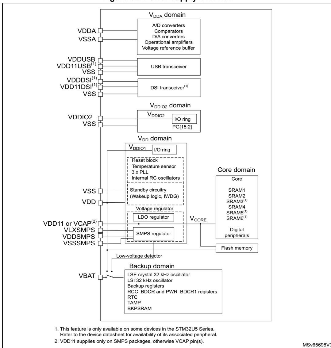
The diagram illustrates the power supply architecture of the device, organized into several domains:
- V DDA domain: Connected to pins VDDA and VSSA. It contains A/D converters, Comparators, D/A converters, Operational amplifiers, and a Voltage reference buffer.
- USB transceiver: Connected to pins VDDUSB, VDD11USB (1) , and VSS.
- DSI transceiver (1) : Connected to pins VDDDSI (1) , VDD11DSI (1) , and VSS.
- V DDIO2 domain: Connected to pins VDDIO2 and VSS. It contains a V DDIO2 I/O ring and PG[15:2].
- V
DD
domain:
Connected to pins VSS, VDD, VDD11 or VCAP
(2)
, VLXSMPS, VDDSMPS, and VSSSMPS. It contains:
- V DDIO1 I/O ring
- Reset block, Temperature sensor, 3 x PLL, Internal RC oscillators
- Standby circuitry (Wakeup logic, IWDG)
- Voltage regulator (containing an LDO regulator and an SMPS regulator)
- Low-voltage detector
- Core domain: Connected to V CORE from the SMPS regulator. It contains the Core, SRAM1, SRAM2, SRAM3 (1) , SRAM4, SRAM5 (1) , SRAM6 (1) , Digital peripherals, and Flash memory.
- Backup domain: Connected to pin VBAT. It contains an LSE crystal 32 kHz oscillator, LSI 32 kHz oscillator, Backup registers, RCC_BDCR and PWR_BDCR1 registers, RTC, TAMP, and BKPSRAM.
Notes:
- This feature is only available on some devices in the STM32U5 Series. Refer to the device datasheet for availability of its associated peripheral.
- VDD11 supplies only on SMPS packages, otherwise VCAP pin(s).
MSv65698V3
10.4.1 External power supplies
The devices require a 1.71 V to 3.6 V V DD operating voltage supply. Several independent supplies can be provided for specific peripherals. These supplies must not be provided without a valid operating supply on VDD pin:
- • V
DD
= 1.71 V to 3.6 V (functionality guaranteed down to V
BOR
minimum value)
V DD is the external power supply for the I/Os, the internal regulator, and the system analog such as reset, power management, and internal clocks. It is provided externally through VDD pins.
- • \( V_{DDA} = 1.58 \text{ V} \) (COMPs) / \( 1.6 \text{ V} \) (DACs, OPAMPs) / \( 1.62 \text{ V} \) (ADCs) / \( 1.8 \text{ V} \) (VREFBUF) to \( 3.6 \text{ V} \)
\( V_{DDA} \) is the external analog power supply for A/D converters, D/A converters, voltage reference buffer, operational amplifiers and comparators. The \( V_{DDA} \) voltage level is independent from the \( V_{DD} \) voltage and must be connected to \( V_{DD} \) or \( V_{SS} \) (preferably to \( V_{DD} \) ) when these peripherals are not used.
- • \( V_{DDSMPS} = 1.71 \text{ V} \) to \( 3.6 \text{ V} \)
\( V_{DDSMPS} \) is the external power supply for the SMPS step-down converter. It is provided externally through \( V_{DDSMPS} \) supply pin, and must be connected to the same supply as \( V_{DD} \) pin when the SMPS is used in the application. When the SMPS is not used, it is recommended to connect both \( V_{DDSMPS} \) and \( V_{LXSMPS} \) to GND.
- • \( V_{LXSMPS} \) is the switched SMPS step-down converter output.
Note: The SMPS power supply pins are available only on a specific package with SMPS step-down converter option.
- • \( V_{DDUSB} = 3.0 \text{ V} \) to \( 3.6 \text{ V} \)
\( V_{DDUSB} \) is the external independent power supply for USB/OTG_FS/OTG_HS transceivers. The \( V_{DDUSB} \) voltage level is independent from the \( V_{DD} \) voltage and must preferably be connected to \( V_{DD} \) when the USB is not used. Internally bonded to \( V_{DD} \) when not available as package pin.
- • \( V_{DD11USB} = 1.0 \text{ V} \) to \( 1.26 \text{ V} \) (only available on STM32U59x/5Ax/5Fx/5Gx devices)
\( V_{DD11USB} \) is the external power supply for the OTG_HS transceiver. This supply is only available on specific packages and must be connected to \( V_{DD11} \) .
- • \( V_{DDIO2} = 1.08 \text{ V} \) to \( 3.6 \text{ V} \)
\( V_{DDIO2} \) is the external power supply for 14 I/Os (port G[15:2]). The \( V_{DDIO2} \) voltage level is independent from the \( V_{DD} \) voltage and must preferably be connected to \( V_{DD} \) when PG[15:2] are not used.
- • \( V_{BAT} = 1.65 \text{ V} \) to \( 3.6 \text{ V} \) (functionality guaranteed down to \( V_{BOR\_VBAT} \) minimum value, refer to the product datasheet)
\( V_{BAT} \) is the power supply when \( V_{DD} \) is not present (through power switch) for RTC, TAMP, external and internal clocks 32 kHz oscillator, backup registers and optionally backup SRAM.
- • \( V_{DDDSI} = 1.71 \text{ V} \) to \( 3.6 \text{ V} \) (only available on STM32U59x/5Ax/5Fx/5Gx devices)
\( V_{DDDSI} \) is the external power supply for the DSI controller. It is provided externally through \( V_{DDDSI} \) supply pin, and must be connected to the same supply as \( V_{DD} \) pin.
- • \( V_{DD11DSI} = 1.0 \text{ V} \) to \( 1.26 \text{ V} \) (only available on STM32U59x/5Ax/5Fx/5Gx devices)
\( V_{DD11DSI} \) is the external power supply for the DSI transceiver and must be connected to \( V_{DD11} \) pin.
- • \( V_{REF-} \) , \( V_{REF+} \)
\( V_{REF+} \) is the input reference voltage for ADCs and DACs. It is also the output of the internal voltage reference buffer when enabled.
\( V_{REF+} \) can be grounded when ADCs and DACs are not active.
The internal voltage reference buffer supports four output voltages, that are configured with VRS bit in the VREFBUF_CSR register:
- – \( V_{REF+} \) around \( 1.5 \text{ V} \) . This requires \( V_{DDA} \geq 1.8 \text{ V} \) .
- – \( V_{REF+} \) around \( 1.8 \text{ V} \) . This requires \( V_{DDA} \geq 2.1 \text{ V} \) .
- – \( V_{REF+} \) around \( 2.048 \text{ V} \) . This requires \( V_{DDA} \geq 2.4 \text{ V} \) .
– \( V_{REF+} \) around 2.5 V. This requires \( V_{DDA} \geq 2.8 \) V.
\( V_{REF-} \) and \( V_{REF+} \) pins are not available on all packages. When not available, they are bonded to \( V_{SSA} \) and \( V_{DDA} \) , respectively.
When the \( V_{REF+} \) is double-bonded with \( V_{DDA} \) in a package, the internal voltage reference buffer is not available and must be kept disabled.
\( V_{REF-} \) must always be equal to \( V_{SSA} \) .
10.4.2 Internal regulators
The devices embed two regulators: one LDO and one SMPS in parallel to provide the \( V_{CORE} \) supply for digital peripherals, SRAMs (except BKPSRAM) and embedded flash memory. The SMPS generates this voltage on \( V_{DD11} \) (two or three pins) with a total external capacitor of 4.7 \( \mu\text{F} \) typical and requires an external coil of 2.2 \( \mu\text{H} \) typical.
The LDO generates this voltage on \( V_{CAP} \) (one or two pins depending on packages) with a total of external capacitor of 4.7 \( \mu\text{F} \) typical.
Both regulators can provide four different voltages (voltage scaling) and can operate in Stop mode.
It is possible to switch from SMPS to LDO and from LDO to SMPS on-the-fly.
10.4.3 Power-up and power-down power sequences
During power-up and power-down phases, the following power sequence requirements must be respected:
- • When \( V_{DD} \) is below 1 V, other power supplies ( \( V_{DDA} \) , \( V_{DDIO2} \) , \( V_{DDUSB} \) ) must remain below \( V_{DD} + 300 \) mV.
- • When \( V_{DD} \) is above 1 V, all power supplies are independent.
During the power-down phase, \( V_{DD} \) can temporarily become lower than other supplies only if the energy provided to the MCU remains below 1 mJ. This allows external decoupling capacitors to be discharged with different time constants during the power-down transient phase.
10.4.4 Independent analog peripherals supply
To improve ADC and DAC conversion accuracy and to extend the supply flexibility, the analog peripherals have an independent power supply that can be separately filtered and shielded from noise on the PCB:
- • The analog peripherals voltage supply input is available on a separate \( V_{DDA} \) pin.
- • An isolated supply ground connection is provided on \( V_{SSA} \) pin.
The \( V_{DDA} \) supply voltage can be different from \( V_{DD} \) . The presence of \( V_{DDA} \) must be checked before enabling any of the analog peripherals supplied by \( V_{DDA} \) (A/D converter, D/A converter, comparators, operational amplifiers, voltage reference buffer).
After reset, the ADC and analog switch control supplied by \( V_{DDA} \) are logically and electrically isolated and therefore are not available. The isolation must be removed before using the analog peripherals, by setting the ASV bit in the PWR_SVMCR register, once the \( V_{DDA} \) supply is present.
The \( V_{DDA} \) supply can be monitored by the analog voltage monitors (AVM), and compared with two thresholds (1.6 V for AVM1 or 1.8 V for AVM2), refer to Section 10.6.3 for more details.
When a single supply is used, \( V_{DDA} \) can be externally connected to \( V_{DD} \) through the external filtering circuit in order to ensure a noise-free \( V_{DDA} \) reference voltage.
ADC and DAC reference voltage
To ensure a better accuracy on low-voltage inputs and outputs, the user can connect to \( V_{REF+} \) , a separate reference voltage lower than \( V_{DDA} \) . \( V_{REF+} \) is the highest voltage, represented by the full scale value, for an analog input (ADC) or output (DAC) signal.
\( V_{REF+} \) can be provided either by an external reference or by an internal buffered voltage reference (VREFBUF). The internal voltage reference can output a configurable voltage: 1.5 V, 1.8 V, 2.048 V or 2.4 V. The internal voltage reference can also provide the voltage to external components through \( V_{REF+} \) pin. Refer to the device datasheet and to Section 36: Voltage reference buffer (VREFBUF) for further information.
10.4.5 Independent I/O supply rail
Some I/Os from port G (PG[15:2]) are supplied from a separate supply rail. The power supply for this rail can range from 1.08 V to 3.6 V and is provided externally through the \( V_{DDIO2} \) pin. The \( V_{DDIO2} \) voltage level is completely independent from \( V_{DD} \) or \( V_{DDA} \) . The \( V_{DDIO2} \) pin is available only for some packages. Refer to the pinout diagrams or tables in the related device datasheet(s) for I/O list(s).
After reset, the I/Os supplied by \( V_{DDIO2} \) are logically and electrically isolated and therefore are not available. The isolation must be removed before using any I/O from PG[15:2], by setting the IO2SV bit in the PWR_SVMCR register, once the \( V_{DDIO2} \) supply is present.
The \( V_{DDIO2} \) supply is monitored by the IO2 voltage monitoring (IO2VM) and compared with the internal reference voltage ( \( 3/4 V_{REFINT} \) , around 0.9 V). Refer to Section 10.6.3 for more details.
10.4.6 Independent USB transceivers supply
The USB transceivers are supplied from a separate \( V_{DDUSB} \) power supply pin.
The \( V_{DDUSB} \) range is from 3.0 V to 3.6 V and is completely independent from \( V_{DD} \) or \( V_{DDA} \) .
After reset, the USB features supplied by \( V_{DDUSB} \) are logically and electrically isolated, and therefore are not available. The isolation must be removed before using USB/OTG_FS/OTG_HS, by setting USV in PWR_SVMCR, once the \( V_{DDUSB} \) supply is present.
The \( V_{DDUSB} \) supply is monitored by the USB voltage monitoring (UVM), and compared with the internal reference voltage ( \( V_{REFINT} \) , around 1.2 V). Refer to Section 10.6.3 for more details.
Internal OTG_HS transceiver supply (STM32U59x/5Ax/5Fx/5Gx only)
The OTG_HS high-speed transceiver is functional in voltage scaling range 1 and range 2. The USB EPOD (embedded power distribution) booster must be enabled and ready before using the OTG_HS: USBPWREN and USBBOOSTEN bits must be set to one in PWR_VOSR (refer to Section 10.6.3 and Section 10.7.12 for more details).
10.4.7 Battery backup domain (also known as RTC domain)
To retain the content of backup registers, backup SRAM, and to supply RTC and TAMP functions when \( V_{DD} \) is turned off, the VBAT pin can be connected to an optional backup voltage supplied by a battery or by another source.
The Backup domain supply is \( V_{SW} \) , which is the output of a power switch between \( V_{DD} \) and \( V_{BAT} \) . The switch between \( V_{DD} \) and \( V_{BAT} \) supplies is automatically controlled by the brownout reset circuitry. This circuitry is not functional in Shutdown mode.
When \( V_{DD} \) is below the lowest brownout reset threshold ( \( V_{BOR0} \) ) in all modes except Shutdown mode, the VBAT pin powers the RTC and TAMP peripherals, the LSI and LSE oscillators. The backup SRAM is optionally powered by VBAT pin when BREN is set in PWR_BDCR1.
The following pin functions are also powered by the VBAT pin:
- • PC13, PC14, and PC15 that can be configured by the RTC, the TAMP, or the LSE (see Section 63.3: RTC functional description )
- • PE3, PE4, PE5, PE6, PC13, PA0, PA1, and PC5 when they are configured by the TAMP as tamper pins
- • PB2 when configured by the RTC as RTC_OUT2 output
When \( V_{DD} \) is higher than \( V_{BOR0} \) , the VDD pin powers all previous functions.
Note: Due to the fact that the analog power switch can transfer only a limited amount of current (3 mA), the use of GPIO PC13 to PC15 in output mode is restricted: the speed must be limited (refer to datasheet for more details) and these I/Os must not be used as a current source (for example to drive a LED).
Warning: During \( t_{RSTTEMPO} \) (temporization at \( V_{DD} \) startup) or after a PDR has been detected, the power switch between \( V_{BAT} \) and \( V_{DD} \) remains connected to \( V_{BAT} \) . During the startup phase, if \( V_{DD} \) is established in less than \( t_{RSTTEMPO} \) (refer to the datasheet for the value of \( t_{RSTTEMPO} \) ) and \( V_{DD} > V_{BAT} + 0.6 \) V, a current may be injected into \( V_{BAT} \) through an internal diode connected between \( V_{DD} \) and the power switch ( \( V_{BAT} \) ). If the power supply/battery connected to the VBAT pin cannot support this current injection, it is strongly recommended to connect an external low-drop diode between this power supply and the VBAT pin.
If no external battery is used in the application, it is recommended to connect \( V_{BAT} \) to \( V_{DD} \) and add a 100 nF ceramic decoupling capacitor on \( V_{BAT} \) pin.
Backup domain access
After a system reset, the backup domain (RCC backup domain control register RCC_BDCR, RTC registers, TAMP registers, backup registers and backup SRAM) is protected against possible unwanted write accesses.
To enable access to the backup domain, proceed as follows:
- 1. Enable the power interface clock by setting the PWREN bits in RCC_AHB3ENR.
- 2. Set the DBP bit in PWR_DBPR to enable access to the backup domain.
V BAT battery charging
When V DD is present, It is possible to charge the external battery on V BAT through an internal resistance.
The V BAT charging is done either through a 5 k \( \Omega \) resistor or through a 1.5 k \( \Omega \) resistor depending on VBRS value in PWR_BDCR2.
The battery charging is enabled by setting VBE in PWR_BDCR2. It is automatically disabled in V BAT mode.
10.5 PWR system supply voltage regulation
10.5.1 SMPS and LDO embedded regulators
The devices embed two internal regulators, that can be selected when the application runs, depending on the application requirements:
- • a SMPS step-down converter
- • a linear voltage regulator (LDO)
The SMPS allows the power consumption to be reduced but some applications can be perturbed by the noise generated by the SMPS, requiring the application to switch to LDO.
The LDO and the SMPS regulators have two modes: main regulator mode (used when performance is needed), and low-power regulator mode. LDO or SMPS can be used in all voltage scaling ranges, and in all Stop modes.
10.5.2 LDO and SMPS versus reset, voltage scaling, and low-power modes
After reset, the regulator is the LDO, in range 4. Switching to SMPS provides lower consumption in particular at high V DD voltage. It is possible to switch from LDO to SMPS, or from SMPS to LDO in any range, by configuring the REGSEL bit.
When exiting Stop or Standby mode, the regulator is the same than when entering low-power modes. The voltage range is the range 4.
Warning: On STM32U59x/5Ax/5Fx/5Gx devices only, when using the device in VOS range 1 at extended temperature ranges (from 85 to 125 °C), the system frequency must be reduced below 110 MHz before switching from LDO to SMPS, or vice versa. It is required to proceed as follow:
- 1. Reduce the system frequency below 110 MHz.
- 2. Configure REGSEL bit to select the required regulator.
- 3. Wait for 8 µs.
- 4. Increase the system frequency to the required frequency.
10.5.3 LDO and SMPS step down converter fast startup
After BOR reset, the LDO and SMPS regulators starts in slow-startup mode. This -startup feature is selected to limit the inrush current after power-on reset. This increases the wake-up time when exiting Stop or Standby mode.
However, it is possible to configure a faster startup on-the-fly, and it is applied for next startup either after a system reset or after a wake-up from low-power mode except Shutdown and \( V_{BAT} \) modes. The fast startup is selected by setting FSTEN in PWR_CR3.
10.5.4 Dynamic voltage scaling management
The dynamic voltage scaling is a power management technique that consists in increasing or decreasing the voltage used for the digital peripherals ( \( V_{CORE} \) ), according to the application performance and power consumption needs.
Dynamic voltage scaling to increase \( V_{CORE} \) is known as overvolting. It allows the device to improve its performance.
Dynamic voltage scaling to decrease \( V_{CORE} \) is known as undervolting. It is performed to save power, particularly in laptop and other mobile devices where the energy comes from a battery and is thus limited.
The regulator operates in the following ranges:
- • Range 1: high performance
It provides a typical output voltage at 1.2 V. It is used when the system clock frequency is up to 160 MHz. - • Range 2: medium-high performance
It provides a typical output voltage at 1.1 V. It is used when the system clock frequency is up to 110 MHz. - • Range 3: medium-low power range
It provides a typical output voltage at 1.0 V. The system clock frequency can be up to 55 MHz. - • Range 4: low-power range
It provides a typical output voltage at 0.9 V. The system clock frequency can be up to 25 MHz.
Voltage scaling is selected through VOS[1:0] in PWR_VOSR. The EPOD (embedded power distribution) booster must be enabled and ready before increasing the system clock frequency above 55 MHz in range 1 and range 2.
The sequence to switch the voltage scaling from range L (lower power) to range P (higher performance) with \( L > P \) , is the following:
- 1. If target SYSCLK > 55 MHz:
- a) Configure PLL1MBOOST[3:0] in RCC_PLL1CFGR to generate a booster clock frequency between 4 and 16 MHz.
- b) Switch on the PLL1 oscillator clock source.
- c) Select the PLL1 clock source (PLL1SRC[1:0] in RCC_PLL1CFGR).
- 2. Program VOS[1:0] to range P in PWR_VOSR.
- 3. Wait until the VOSRDY flag is set in PWR_VOSR.
- 4. If target SYSCLK > 55 MHz:
- a) Set BOOSTEN in PWR_VOSR. This step can be done together with VOS programming.
- b) Wait until the BOOSTRDY flag is set in PWR_VOSR.
- 5. Adjust number of wait states according new frequency target in range P (LATENCY bits in FLASH_ACR, and WSC bits in RAMCFG_MxCR).
- 6. Configure and enable the PLL if needed.
- 7. Configure and switch to new system frequency.
The sequence to switch the voltage scaling from range P (higher performance) to range L (lower power) with L > P, is the following:
- 1. Reduce the system frequency to a value lower than range L maximum frequency.
- 2. Adjust number of wait states according new frequency target (LATENCY bits in FLASH_ACR and WSC bits in the RAMCFG_MxCR).
- 3. If new SYSCLK \( \leq \) 55 MHz, clear BOOSTEN in PWR_VOSR if it was set.
- 4. Program VOS bits to range L in PWR_VOSR. This step can be done together with BOOSTEN clearing.
System frequency steps on STM32U59x/5Ax/5Fx/5Gx devices
On STM32U59x/5Ax/5Fx/5Gx devices only, the maximum system frequency increase or decrease in the VOS range 1 is 80 MHz.
The sequence to increase the frequency in the VOS range 1 above 80 MHz is the following:
- 1. Divide the system clock by two, using the AHB prescaler (HPRE = 0b1000 in RCC_CFGR2).
- 2. Configure and enable the PLL1 if needed.
- 3. Select PLL1 as system clock source (SW = 0b11 in RCC_CFGR1).
- 4. Wait for 5 \( \mu \) s.
- 5. Set the AHB prescaler to 1 (HPRE = 0b0000 in RCC_CFGR2).
When running at higher frequencies than 80 MHz in the VOS range 1, the sequence to decrease the frequency is the following:
- 1. Divide the system clock by two using the AHB prescaler (HPRE = 0b1000 in RCC_CFGR2).
- 2. Wait for 5 \( \mu \) s.
- 3. Define the lower speed clock as system clock source.
- 4. Set the AHB prescaler back to 1 (HPRE = 0b0000 in RCC_CFGR2).
In other VOS ranges, there is no limitation during system frequency increase or decrease.
10.6 PWR power-supply supervision
10.6.1 Brownout reset (BOR)
The device has an integrated brownout reset (BOR) circuitry. The BOR is active in all power modes except Shutdown mode, and cannot be disabled.
Five BOR thresholds can be selected through option bytes. BOR0 provides the always enabled power-on/power-down functionality, independent from any other higher BOR level selection.
During power-on, the BOR keeps the device under reset until the supply voltage \( V_{DD} \) reaches the specified \( V_{BORx} \) threshold. When \( V_{DD} \) drops below the selected threshold, a device reset is generated. When \( V_{DD} \) is above the \( V_{BORx} \) upper limit, the device reset is released and the system can start.
For more details on the brownout reset thresholds, refer to the electrical characteristics section in the datasheet.
During Standby mode, and if BOR level 0 is selected, it is possible to set the BOR in ultra-low-power mode to further reduce the current consumption by setting ULPMEN in PWR_CR1.
Figure 33. Brownout reset waveform
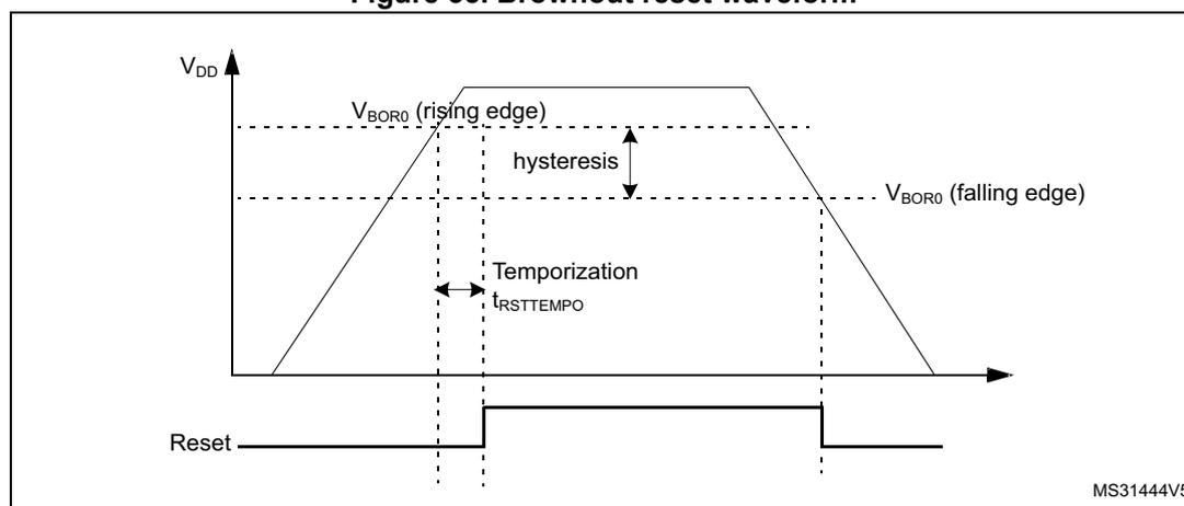
- 1. The reset temporization \( t_{RSTTEMPO} \) is present only for the BOR lowest threshold ( \( V_{BOR0} \) ).
Note: BOR is not functional in Shutdown mode.
10.6.2 Programmable voltage detector (PVD)
The PVD can be used to monitor the \( V_{DD} \) power supply by comparing it to a threshold selected by PVDLS[2:0] in PWR_SVMCR.
The PVD is enabled by setting PVDE bit.
A PVDO flag is available in PWR_SVMCR to indicate if \( V_{DD} \) is higher or lower than the PVD threshold. This event is internally connected to the EXTI, and can generate an interrupt if enabled through the EXTI registers (refer to Table 110 ).
The rising/falling edge sensitivity of the EXTI Line must be configured according to PVD output behavior. For example, if the EXTI line is configured to rising edge sensitivity, the
interrupt is generated when \( V_{DD} \) drops below the PVD threshold. As an example, the service routine can perform emergency shutdown tasks.
The PVD can remain active in Stop 0, Stop 1, and Stop 2 modes, and the PVM interrupt can wake up from Stop mode. The PVD is not functional in Stop 3 mode.
Figure 34. PVD thresholds
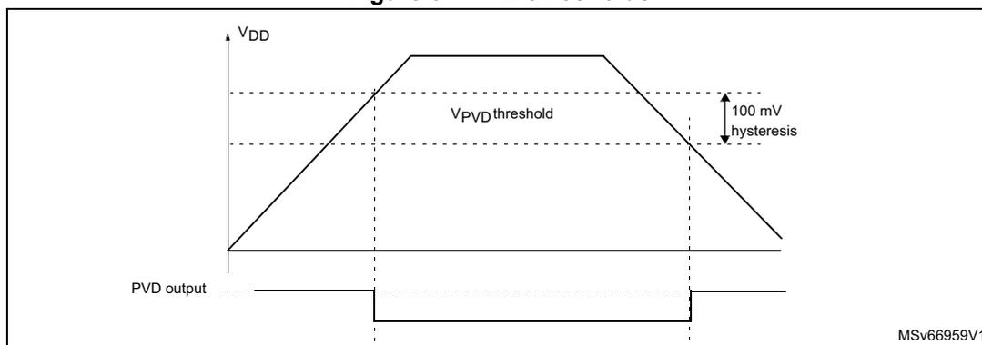
Note: PVD is not functional in Shutdown mode.
10.6.3 Peripheral voltage monitoring (PVM)
Only \( V_{DD} \) is monitored by default, as it is the only supply required for all system-related functions. The other supplies ( \( V_{DDA} \) , \( V_{DDIO2} \) , and \( V_{DDUSB} \) ) can be independent from \( V_{DD} \) and can be monitored with four peripheral voltage monitoring (PVM):
- • The UVM monitors the USB supply \( V_{DDUSB} \) . VDDUSBRDY indicates if the \( V_{DDUSB} \) independent power supply is higher or lower than the \( V_{UVM} \) threshold.
- • The IO2VM monitors the PG[15:2] supply \( V_{DDIO2} \) . VDDIO2RDY indicates if the \( V_{DDIO2} \) independent power supply is higher or lower than the \( V_{IO2VM} \) threshold.
- • The AVM1 monitors the analog supply \( V_{DDA} \) . VDDA1RDY indicates if the \( V_{DDA} \) independent power supply is higher or lower than the \( V_{AVM1} \) threshold.
- • The AVM2 monitors the analog supply \( V_{DDA} \) . VDDA2RDY indicates if the \( V_{DDA} \) independent power supply is higher or lower than the \( V_{AVM2} \) threshold.
Each PVM output is connected to an EXTI line and can generate an interrupt if enabled through the EXTI registers. The PVMx output interrupt is generated when the independent power supply drops below the PVM threshold and/or when it rises above the PVM threshold, depending on EXTI line rising/falling edge configuration (refer to Table 110 ).
Each PVM can remain active in Stop 0, Stop 1, and Stop 2 modes, and the PVM interrupt can wake up from the Stop mode. The PVM is not functional in Stop 3 mode.
Table 98. PVM features
| PVM | Power supply | PVM threshold |
|---|---|---|
| UVM | \( V_{DDUSB} \) | \( V_{UVM} \) (around 1.2 V) |
| IO2VM | \( V_{DDIO2} \) | \( V_{IO2VM} \) (around 0.9 V) |
| AVM1 | \( V_{DDA} \) | \( V_{AVM1} \) (around 1.6 V) |
| AVM2 | \( V_{DDA} \) | \( V_{AVM2} \) (around 1.8 V) |
The independent supplies ( \( V_{DDA} \) , \( V_{DDIO2} \) , and \( V_{DDUSB} \) ) are not considered as present by default, and a logical and electrical isolation is applied to ignore any information coming from the peripherals supplied by these dedicated supplies:
- • If these supplies are shorted externally to \( V_{DD} \) , the application assumes they are available without enabling any peripheral voltage monitoring.
- • If these supplies are independent from \( V_{DD} \) , the peripheral voltage monitoring (PVM) can be enabled to confirm whether the supply is present or not.
The following sequence must be done before using the USB/OTG_FS/OTG_HS:
- 1. If
\(
V_{DDUSB}
\)
is independent from
\(
V_{DD}
\)
:
- a) Enable the UVM by setting UVMEN in PWR_SVMCR.
- b) Wait for the UVM wake-up time.
- c) Wait until VDDUSBRDY is set in PWR_SVMSR.
- d) Disable the UVM for consumption saving (optional).
- 2. Set USV in PWR_SVMCR to remove the \( V_{DDUSB} \) power isolation.
- 3. On STM32U59x/5Ax/5Fx/5Gx devices only:
- a) Make sure the voltage scaling is in range 1 or in range 2 (using VOS[1:0] in PWR_VOSR).
- b) Make sure the EPOD booster clock is enabled (using PLL1MBOOST[3:0] in RCC_PLL1CFGGR).
- c) Enable the USB internal power by setting USBPWREN and USBBOOSTEN in PWR_VOSR.
- d) Wait for USBBOOSTRDY to be set in PWR_VOSR.
The following sequence must be done before using any I/O from PG[15:2]:
- 1. If
\(
V_{DDIO2}
\)
is independent from
\(
V_{DD}
\)
:
- a) Enable the IO2VM by setting IO2VM in PWR_SVMCR.
- b) Wait for the IO2CVM wake-up time.
- c) Wait until VDDIO2RDY is set in PWR_SVMSR.
- d) Disable the IO2VM for consumption saving (optional).
- 2. Set IO2SV in PWR_SVMCR to remove the \( V_{DDIO2} \) power isolation.
The following sequence must be done before using any of these analog peripherals: analog to digital converters, digital to analog converters, comparators, operational amplifiers, voltage reference buffer:
- 1. If
\(
V_{DDA}
\)
is independent from
\(
V_{DD}
\)
:
- a) Enable the AVM1 or AVM2 by setting AVM1EN or AVM2EN in PWR_SVMCR.
- b) Wait for the AVM wake-up time.
- c) Wait until VDDA1RDY or VDDA2RDY is set in PWR_SVMCR.
- d) Disable the AVM for consumption saving (optional).
- 2. Set the ASV in PWR_SVMCR to remove the \( V_{DDA} \) power isolation.
Note: PVM is not functional in Shutdown mode.
10.6.4 Backup domain voltage and temperature monitoring
When the backup domain voltage and temperature monitoring is enabled (MONEN = 1 in PWR_DBPR), the backup domain voltage and the temperature are monitored. This monitoring is not functional in Shutdown mode.
If the backup domain voltage monitoring internal tamper is enabled in the TAMP peripheral (ITAMP1E = 1 in TAMP_CR1), a tamper event is generated when the backup domain voltage is above the functional range. In case the backup domain voltage is below the functional range, a brownout reset is generated, erasing all device including backup domain.
Note: The backup domain voltage is \( V_{DD} \) when present, \( V_{BAT} \) otherwise.
If the temperature monitoring internal tamper is enabled in the TAMP peripheral (ITAMP2E = 1 in TAMP_CR1), a tamper event is generated when the temperature is above or below the functional range.
Note: Backup domain voltage and temperature monitoring is not functional in Shutdown mode.
10.7 PWR power management
10.7.1 Power modes
By default, the microcontroller is in Run mode after a system or a power reset. Reducing the power consumption in Run mode is done by configuring the voltage scaling according to application performance needs. Refer to Section 10.5.4 for more details. Unused RAMs can be powered-off with SRAMxPD bits in PWR_CR1. The power consumption is also reduced by reducing SYSCLK, HCLK, and PCLK clocks speed, or gating unused peripherals clocks. Refer to Section 11: Reset and clock control (RCC) for more details.
Several low-power modes are available to save power when the CPU does not need to be kept running, for example when waiting for an external event. It is up to the user to select the mode that gives the best compromise between low-power consumption, short startup time and available wake-up sources.
The device features these low-power modes:
- • Sleep mode:
CPU clock off, all peripherals including Cortex-M33 core such as NVIC and SysTick can run and wake up the CPU when an interrupt or an event occurs. Refer to Section 10.7.5 . - • Stop 0, Stop 1, Stop 2, Stop 3 modes:
Stop mode achieves the lowest power consumption while retaining the content of SRAM and registers. The SRAMs can be totally or partially switched off to further reduce consumption. All clocks in the core domain are stopped. The PLL, the MSI (MSIS and MSIK) RC, the HSI16 RC and the HSE crystal oscillators are disabled. The LSE or LSI is still running.
The RTC can remain active (Stop mode with RTC, Stop mode without RTC).
Some peripherals are autonomous and can operate in Stop mode by requesting their kernel clock and their bus (APB or AHB) when needed, in order to transfer data with DMA (GPDMA1 or LPDMA1 depending on peripherals and power mode).
In Stop 2 and Stop 3 modes, most of the core domain is put in a lower leakage mode. Stop 0 and Stop 1 offers the largest number of active peripherals and wake-up sources,
a smaller wake-up time but a higher consumption than Stop 2.
In Stop 0 mode, the regulator remains in main regulator mode, allowing a very fast wake-up time but with much higher consumption.
Stop 3 is the lowest power mode with full retention, but the functional peripherals and sources of wake-up are reduced to the same ones than in Standby mode.
The system clock when exiting from Stop mode can be either MSIS up to 24 MHz or HSI16, depending on software configuration.
Refer to Section 10.7.6 , Section 10.7.7 , Section 10.7.8 and Section 10.7.9 .
- • Standby mode:
The Standby mode is used to achieve the lowest power consumption with BOR. The internal regulator is switched off so that the core domain is powered off. The PLL, the MSI (MSIS and MSIK) RC, the HSI16 RC and the HSE crystal oscillators are also switched off.
The RTC can remain active (Standby mode with RTC, Standby mode without RTC).
The brownout reset (BOR) always remains active in Standby mode.
The state of each I/O during Standby mode can be selected by software: I/O with internal pull-up, internal pull-down or floating.
After entering Standby mode, SRAMs and register contents are lost except for registers and backup SRAM in the backup domain and Standby circuitry. Optionally, the full SRAM2 or 8 Kbytes or 56 Kbytes can be retained in Standby mode, supplied by the low-power regulator (standby with SRAM2 retention mode).
The BOR can be configured in ultra-low-power mode to further reduce power consumption during standby mode and when the lowest threshold is selected ( \( V_{BOR0} \) ).
The device exits Standby mode when an external reset (NRST pin), an IWDG reset, WKUP pin event (configurable rising or falling edge), a RTC event occurs (alarm, periodic wake-up, timestamp), or a tamper detection. The tamper detection can be raised either due to external pins or due to an internal failure detection.
The system clock after wake-up is MSIS up to 4 MHz.
Refer to Section 10.7.10 .
- • Shutdown mode:
The Shutdown mode allows the lowest power consumption. The internal regulator is switched off so that the core domain is powered off. The PLL, the HSI16, the MSI (MSIS and MSIK), the LSI and the HSE oscillators are also switched off.
The RTC can remain active (Shutdown mode with RTC, Shutdown mode without RTC). The BOR is not available in Shutdown mode. No power voltage monitoring is possible in this mode, therefore the switch to backup domain is not supported.
SRAMs and register contents are lost except for registers in the backup domain.
The device exits Shutdown mode when an external reset (NRST pin), a WKUP pin event (configurable rising or falling edge), or a RTC event occurs (alarm, periodic wake-up, timestamp), or a tamper detection.
The system clock after wake-up is MSIS at 4 MHz. Refer to Section 10.7.11 .
The table below shows the power modes overview.
Table 99. Low-power mode summary
| Mode name | Entry | Wake-up source (1) | Wake-up system clock | Effect on clocks | Voltage regulators |
|---|---|---|---|---|---|
| Sleep (Sleep-now or Sleep-on-exit) | WFI or Return from ISR | Any interrupt except OTG_FS, USB, and UCPD in range 4 – OTG_HS in range 3 and 4 | Same as before entering Sleep mode | CPU clock OFF No effect on other clocks or analog clock sources | Range 1, 2, 3, 4 |
| WFE | Wake-up event | ||||
| Stop 0 | LPMS = 000 + SLEEPDEEP bit + WFI or Return from ISR or WFE | Any EXTI line (configured in the EXTI registers) Specific peripherals events/interrupts (2) | HSI16 when STOPWUCK = 1 in RCC_CFGR1 MSIS with the frequency before entering the Stop mode, limited to 24 MHz, when STOPWUCK = 0 | All clocks OFF except LSI and LSE | Range 1, 2, 3, 4 |
| Stop 1 | LPMS = 001 + SLEEPDEEP bit + WFI or Return from ISR or WFE | MSIK, MSIS, or HSI16 can be enabled temporarily when requested by an autonomous peripheral, or forced to be kept enabled. | Low-power regulator (SMPS or LDO) | ||
| Stop 2 | LPMS = 010 + SLEEPDEEP bit + WFI or Return from ISR or WFE | ||||
| Stop 3 | LPMS = 011 + SLEEPDEEP bit + WFI or Return from ISR or WFE | WKUP pin edge, RTC/TAMP events/interrupts (2), external reset in NRST pin, IWDG reset | MSIS from 1 MHz up to 4 MHz | All clocks OFF except LSI and LSE | OFF |
| Standby with SRAM2_ 8 Kbytes | LPMS = 10x+ RRS1 = 1 + SLEEPDEEP bit + WFI or Return from ISR or WFE | ||||
| Standby with SRAM2_Full | LPMS = 10x+ RRS1 = RRS2 = 1+ SLEEPDEEP bit + WFI or Return from ISR or WFE | ||||
| Standby | LPMS = 10x + RRS1 = RRS2 = 0 + SLEEPDEEP bit + WFI or Return from ISR or WFE | WKUP pin edge, RTC/TAMP events/interrupts (2), external reset in NRST pin | MSIS 4 MHz | All clocks off except LSE | OFF |
| Shutdown | LPMS = 11x + SLEEPDEEP bit + WFI or Return from ISR or WFE |
- 1. Refer to Table 100 .
- 2. A wake-up event can be generated with the peripheral interrupt signal. Refer to Section : Exiting a low-power mode .
Table 100. Functionalities depending on the working mode (1)
| Peripheral | Run | Sleep | Stop 0/1 | Stop 2 | Stop 3 | Standby | Shutdown | VBAT | |||||
|---|---|---|---|---|---|---|---|---|---|---|---|---|---|
| - | Wake-up capability | - | Wake-up capability | - | Wake-up capability | - | Wake-up capability | - | Wake-up capability | ||||
| CPU | Y | - | - | - | - | - | - | - | - | - | - | - | - |
| Flash memory | O (2) | O (2) | - | (5) | - | - | - | - | - | - | - | - | - |
| SRAM1 | Y (3) | Y (4) | O (8) | - | O (8) | - | O (8) | - | - | - | - | - | - |
| SRAM2 | Y (3) | Y (4) | O (8) | O (5) | O (8) | - | O (8) | - | O (6) | - | - | - | - |
| SRAM3 (7) | Y (3) | Y (4) | O (8) | O (5) | O (8) | - | O (8) | - | - | - | - | - | - |
| SRAM4 | Y (3) | Y (4) | O (8) | - | O (8) | - | O (8) | - | - | - | - | - | - |
| SRAM5 (7) | Y (3) | Y (4) | O (8) | - | O (8) | - | O (8) | - | - | - | - | - | - |
| SRAM6 (7) | Y (3) | Y (4) | O (8) | - | O (8) | - | O (8) | - | - | - | - | - | - |
| BKPSRAM | O | O | O | O (5) | O | - | O | - | O | - | - | - | O |
| FSMC | O | O | - | - | - | - | - | - | - | - | - | - | - |
| OCTOSPIx (7) (x =1,2) | O | O | - | - | - | - | - | - | - | - | - | - | - |
| HSPI1 (7) | O | O | - | - | - | - | - | - | - | - | - | - | - |
| Backup registers | Y | Y | Y | - | Y | - | Y | - | Y | - | Y | - | Y |
| Brownout reset (BOR) | Y | Y | Y | Y | Y | Y | Y | Y | Y | Y | - | - | - |
| Programmable voltage detector (PVD) | O | O | O | O | O | O | - | - | - | - | - | - | - |
| Peripheral voltage monitor | O | O | O | O | O | O | - | - | - | - | - | - | - |
| GPDMA | O | O | O | O (9) | - | - | - | - | - | - | - | - | - |
| LPDMA | O | O | O | O (10) | O | O (10) | - | - | - | - | - | - | - |
| DMA2D (7) | O | O | - | - | - | - | - | - | - | - | - | - | - |
| High-speed internal (HSI16) | O | O | (11) | - | (11) | - | - | - | - | - | - | - | - |
| Oscillator HSI48 | O | O | - | - | - | - | - | - | - | - | - | - | - |
| High-speed external (HSE) | O | O | - | - | - | - | - | - | - | - | - | - | - |
| Low-speed internal (LSI) | O | O | O | - | O | - | O | - | O | - | - | - | O |
| Peripheral | Run | Sleep | Stop 0/1 | Stop 2 | Stop 3 | Standby | Shutdown | VBAT | |||||
|---|---|---|---|---|---|---|---|---|---|---|---|---|---|
| - | Wake-up capability | - | Wake-up capability | - | Wake-up capability | - | Wake-up capability | - | Wake-up capability | ||||
| Low-speed external (LSE) | O | O | O | - | O | - | O | - | O | - | O | - | O |
| Multi-speed internal (MSIS and MSIK) | O | O | (11) | - | (11) | - | - | - | - | - | - | - | - |
| Clock security system (CSS) | O | O | - | - | - | - | - | - | - | - | - | - | - |
| Clock security system on LSE | O | O | O | O | O | O | O | O | O | O | O | O | O |
| Backup domain voltage monitoring, temperature monitoring | O | O | O | O | O | O | O | O | O | O | - | - | O |
| RTC/TAMP | O | O | O | O | O | O | O | O | O | O | O | O | O |
| Number of TAMP tamper pins | 8 | 8 | 8 | O | 8 | O | 8 | O | 8 | O | 8 | O | 8 |
| OTG_FS (7) , OTG_HS (7) , USB (7) , UCPD (7) | O (12) | O (12) | - | O (13) | - | - | - | - | - | - | - | - | - |
| USARTx (x=1,2 (7) ,3,4,5,6 (7) ) | O | O | O (14) | O (14) | - | - | - | - | - | - | - | - | - |
| Low-power UART (LPUART) | O | O | O (14) | O (14) | O (14) | O (14) | - | - | - | - | - | - | - |
| I2Cx (x = 1,2,4,5 (7) ,6 (7) ) | O | O | O (15) | O (15) | - | - | - | - | - | - | - | - | - |
| I2C3 | O | O | O (15) | O (15) | O (15) | O (15) | - | - | - | - | - | - | - |
| SPIx (x = 1,2) | O | O | O (16) | O (16) | - | - | - | - | - | - | - | - | - |
| SPI3 | O | O | O (16) | O (16) | O (16) | O (16) | - | - | - | - | - | - | - |
| FDCAN1 | O | O | - | - | - | - | - | - | - | - | - | - | - |
| SDMMCx (x = 1,2 (7) ) | O | O | - | - | - | - | - | - | - | - | - | - | - |
| SAIx (x = 1,2 (7) ) | O | O | - | - | - | - | - | - | - | - | - | - | - |
| ADCx (x = 1,2 (7) ) | O | O | - | - | - | - | - | - | - | - | - | - | - |
| ADC4 | O | O | O (17) | O (17) | O (17) | O (17) | - | - | - | - | - | - | - |
| DAC1 (2 converters) | O | O | O | - | O | - | - | - | - | - | - | - | - |
| VREFBUF | O | O | O | - | O | - | - | - | - | - | - | - | - |
| OPAMPx (x = 1,2) | O | O | O | - | O | - | - | - | - | - | - | - | - |
| COMPx (x = 1,2) | O | O | O | O | O | O | - | - | - | - | - | - | - |
Table 100. Functionalities depending on the working mode (1) (continued)
| Peripheral | Run | Sleep | Stop 0/1 | Stop 2 | Stop 3 | Standby | Shutdown | VBAT | |||||
|---|---|---|---|---|---|---|---|---|---|---|---|---|---|
| - | Wake-up capability | - | Wake-up capability | - | Wake-up capability | - | Wake-up capability | - | Wake-up capability | ||||
| Temperature sensor | O | O | O | - | O | - | - | - | - | - | - | - | - |
| Timers (TIMx) | O | O | - | - | - | - | - | - | - | - | - | - | - |
| GFXTIM (7) | O | O | - | - | - | - | - | - | - | - | - | - | - |
| LPTIMx (x = 1,3,4) | O | O | O (18) | O (18) | O (18) | O (18) | - | - | - | - | - | - | - |
| LPTIM2 | O | O | O (18) | O (18) | - | - | - | - | - | - | - | - | - |
| Independent watchdog (IWDG) | O | O | O | O | O | O | O | O | O | O | - | - | - |
| Window watchdog (WWDG) | O | O | - | - | - | - | - | - | - | - | - | - | - |
| SysTick timer | O | O | - | - | - | - | - | - | - | - | - | - | - |
| Multi-function digital filter (MDF) | O | O | O (19) | O (19) | - | - | - | - | - | - | - | - | - |
| Audio digital filter (ADF) | O | O | O (19) | O (19) | O (19) | O (19) | - | - | - | - | - | - | - |
| LTDC (7) | O | O | - | - | - | - | - | - | - | - | - | - | - |
| DSI (7) | O (20) | O (20) | - | - | - | - | - | - | - | - | - | - | - |
| GFXMMU (7) | O | O | - | - | - | - | - | - | - | - | - | - | - |
| GPU2D (7) | O | O | - | - | - | - | - | - | - | - | - | - | - |
| JPEG (7) | O | O | - | - | - | - | - | - | - | - | - | - | - |
| Digital camera interface (DCMI) | O | O | - | - | - | - | - | - | - | - | - | - | - |
| Parallel synchronous slave interface (PSSI) | O | O | - | - | - | - | - | - | - | - | - | - | - |
| CORDIC co-processor (CORDIC) | O | O | - | - | - | - | - | - | - | - | - | - | - |
| Filter mathematical accelerator (FMAC) | O | O | - | - | - | - | - | - | - | - | - | - | - |
| Touch sensing controller (TSC) | O | O | - | - | - | - | - | - | - | - | - | - | - |
| Random number generator (RNG) | O | O | - | - | - | - | - | - | - | - | - | - | - |
| AES and secure AES (7) | O | O | - | - | - | - | - | - | - | - | - | - | - |
| Peripheral | Run | Sleep | Stop 0/1 | Stop 2 | Stop 3 | Standby | Shutdown | VBAT | |||||
|---|---|---|---|---|---|---|---|---|---|---|---|---|---|
| - | Wake-up capability | - | Wake-up capability | - | Wake-up capability | - | Wake-up capability | - | Wake-up capability | ||||
| Public key accelerator (PKA) (7) | O | O | - | - | - | - | - | - | - | - | - | - | - |
| On-the-fly decryption (OTFDEC) (7) | O | O | - | - | - | - | - | - | - | - | - | - | - |
| HASH accelerator | O | O | - | - | - | - | - | - | - | - | - | - | - |
| CRC calculation unit | O | O | - | - | - | - | - | - | - | - | - | - | - |
| GPIOs | O | O | O | O | O | O | (21) 24 pins | (21) 24 pins | (21) 24 pins | (21) 24 pins | (22) 24 pins | (22) 24 pins | - |
- 1. Y = yes (enable). O = optional (disable by default, can be enabled by software). - = not available. Gray cells highlight the wake-up capability in each mode.
- 2. The flash memory can be configured in power-down mode. By default, it is not in power-down mode.
- 3. The SRAMs can be powered on or off independently.
- 4. The SRAM clock can be gated on or off independently.
- 5. ECC error interrupt or NMI wakes up from this Stop mode.
- 6. 8 Kbytes, 56 Kbytes or full SRAM2 content can be preserved.
- 7. This feature is only available on some STM32U5 Series devices. Refer to the device datasheet for availability of its associated peripheral.
- 8. Sub-blocks or full SRAM1, SRAM3, SRAM5, SRAM6, full SRAM2 and SRAM4 can be powered-off to save power consumption. SRAM1, SRAM2, SRAM3, SRAM4, SRAM5, and SRAM6 can be accessed by GPDMA in Stop 0 and Stop 1 modes. SRAM4 can be accessed by LPDMA in Stop 0, Stop 1, and Stop 2 modes.
- 9. GPDMA transfers are functional and autonomous in Stop mode, and generates a wake-up interrupt on transfer events.
- 10. LPDMA transfers are functional and autonomous in Stop mode, and generates a wake-up interrupt on transfer events.
- 11. Some peripherals with autonomous mode and wake-up from Stop capability can request HSI16, MSIS or MSIK to be enabled. In this case, the oscillator is woken up by the peripheral, and is automatically put off when no peripheral needs it.
- 12. OTG_FS and USB are functional in voltage scaling range 1, 2, and 3. OTG_HS is functional in voltage scaling range 1 and 2.
- 13. OTG_HS cannot wake up from Stop 1 mode.
- 14. USART and LPUART reception and transmission is functional and autonomous in Stop mode, in asynchronous, and in SPI master modes, and generates a wake-up interrupt on transfer events.
- 15. I2C reception and transmission is functional and autonomous in Stop mode, and generates a wake-up interrupt on transfer events.
- 16. SPI reception and transmission is functional and autonomous in Stop mode, and generates a wake-up interrupt on transfer events.
- 17. ADC conversion is functional and autonomous in Stop mode, and generates a wake-up interrupt on conversion events.
- 18. LPTIM is functional and autonomous in Stop mode, and generates a wake-up interrupt on events.
- 19. MDF and ADF is functional and autonomous in Stop mode, and generates a wake-up interrupt on events.
- 20. DSI is functional in voltage scaling range 1 and 2.
- 21. I/Os can be configured with internal pull-up, pull-down or floating in Standby mode.
- 22. I/Os can be configured with internal pull-up, pull-down or floating in Shutdown mode but the configuration is lost when exiting Shutdown mode.
In addition, the power consumption in Run mode can be reduced by one of the following means:
- • Slowing down the system clocks and configuring voltage scaling to lower-power ranges.
- • Gating the clocks to the APB and AHB peripherals when they are unused.
- • Powering off unused RAMs
When a SRAM has been powered off, it can be powered on again by following the procedure:
- 1. Reset SRAMxPD in PWR_CR1.
- 2. Wait for 1.6 µs.
- 3. Set SRAMxEN in RCC_AHBxENR.
Debug mode
By default, the debug connection is lost if the application puts the MCU in Stop 0, Stop 1, Stop 2, Stop 3, Standby, or Shutdown mode while the debug features are used. This is due to the fact that the Cortex-M33 core is no longer clocked.
However, by setting some configuration bits in the DBGMCU control registers, the software can be debugged even when using the low-power modes extensively. For more details, refer to Section 75.2.5: Debug and low-power modes .
10.7.2 Autonomous peripherals and low-power background autonomous mode (LPBAM)
Several peripherals support the autonomous mode which allows it to be functional and perform DMA transfers in Stop 0, Stop 1, and Stop 2 modes, allowing to build more complex use cases with autonomous peripherals, without any CPU wake-up thanks to DMA transfers. Autonomous transfers using LPDMA, available down to Stop2, can be configured using the LPBAM tool.
Stop 0 and Stop 1 modes
In Stop 0 and Stop 1 modes, the autonomous peripherals are ADC4, DAC1, LPTIMx (x = 1 to 4), USARTx (x = 1 to 6), LPUART1, SPIx (x = 1 to 3), I2Cx (x = 1 to 6), MDF1, ADF1, GPDMA1 and LPDMA1:
- • ADC4, DAC1, LPTIM1, LPTIM3, LPUART1, SPI3, I2C3 and ADF1 are autonomous only with LPDMA1 and SRAM4.
- • LPTIM2, USARTx (x = 1 to 6), SPI1, SPI2, I2C1, I2C2, I2C4, I2C5, I2C6, and MDF1 are autonomous only with GPDMA1 and SRAM1 to SRAM6.
Stop 2 mode
In Stop 2 mode, the autonomous peripherals are ADC4, DAC1, LPTIM1, LPTIM3, LPUART1, SPI3, I2C3, ADF1, and LPDMA1. In this mode, the SRAM4 can be accessed by the LPDMA1.
Autonomous peripherals and LPBAM features
These autonomous peripherals support the following features:
- • Functionality in Stop mode thanks to its own independent clock (named kernel clock) request capability: the peripheral kernel clock is automatically switched on when
requested by a peripheral, and automatically switched off when no peripheral requests it.
- • DMA transfers supported in Stop mode thanks to the system clock request capability: the system clock (MSIS or HSI16) automatically switched on when requested by a peripheral, and automatically switched off when no peripheral requests it. When the system clock is requested by an autonomous peripheral, the system clock is woken up and distributed to all peripherals enabled in the RCC. This allows the DMA to access the enabled SRAM, and any enabled peripheral register (for instance GPIO or LPGPIO registers).
- • Automatic start of the peripheral thanks to the hardware synchronous or asynchronous triggers (such as I/Os edge detection and low-power timer event)
- • wake-up from Stop mode with peripheral interrupt
The GPDMA1 and LPDMA1 are fully functional and the linked-list is updated in Stop mode, allowing the different DMA transfers to be linked without any CPU wake-up. This can be used to chain different peripherals transfers, or to write peripherals registers in order to change their configuration while remaining in Stop mode. LPBAM application drivers and tools are available in STM32CubeMX, to help building those peripherals scenarios in Stop 2 mode, thanks to LPDMA1 linked-list transfers.
The DMA transfers from memory to memory can be started by hardware synchronous or asynchronous triggers, and the DMA transfers between peripherals and memories can also be gated by those triggers.
Here below some use-cases that can be done while remaining in Stop mode:
- • ADC or DAC conversion triggered by a low-power timer (or any other trigger)
- – Wake-up from Stop mode on analog watchdog if the ADC conversion result is out of the programmed thresholds
- – Wake-up from Stop mode on DMA buffer event
- • Audio digital filter data transfer into SRAM
- – Wake-up from Stop on sound activity detection
- • I2C slave reception or transmission, SPI reception, UART/LPUART reception
- – Wake-up at the end of peripheral transfer or on DMA buffer event
- • I2C master transfer, SPI transmission, UART/LPUART transmission, triggered by a low-power timer (or any other trigger)
- – Example: sensor periodic read
- – Wake-up at the end of peripheral transfer or on DMA buffer event
- • Bridges between peripherals
- – Example: ADC converted data transferred by communication peripherals
- • Data transfer from/to GPIO/LPGPIO to/from SRAM for:
- – Controlling external components
- – Implementing data transmission and reception protocols
- • Data transfer from a SRAM to another one
10.7.3 Run mode
Slowing down system clocks
In Run mode, the speed of the system clocks (SYSCLK, HCLK, PCLK) can be reduced by programming the prescaler registers. These prescalers can also be used to slow down the peripherals before entering the Sleep mode.
For more details, refer to Section 11: Reset and clock control (RCC) .
Peripheral clock gating
In Run mode, the HCLK and PCLK for individual peripherals and memories can be stopped at any time to reduce the power consumption.
To further reduce the power consumption in Sleep mode, the peripheral clocks can be disabled prior to executing the WFI or WFE instructions.
The peripheral clock gating is controlled by the RCC_AHBxENR and RCC_APBxENR registers.
Disabling the peripherals clocks in Sleep mode can be performed automatically by resetting the corresponding bit in the RCC_AHBxSMENR and RCC_APBxSMENR registers. This bit must be set for the peripherals requesting clocks in Stop mode for autonomous DMA transfers or to generate a wake-up interrupt.
Disabling the peripherals autonomous clock in Stop 2 mode can be performed automatically by resetting the corresponding bit in RCC_AHB3SMENR and RCC_APB3SMENR.
10.7.4 Low-power modes
Entering into a low-power mode
The MCU enters in low-power modes by executing the WFI (wait for interrupt), or WFE except for Stop 3 mode (wait for event) instructions, or when the SLEEPONEXIT bit in the Cortex-M33 system control register is set on Return from ISR .
Entering into a low-power mode through WFI or WFE is executed only if no interrupt is pending or no event is pending.
Caution: The peripherals with autonomous mode feature are able to generate an AHB or APB clock request, depending on their internal events. If a clock request is present when WFI or WFE is executed, the low-power mode entry is delayed until the clock request is released.
Exiting a low-power mode
The way the MCU exits Sleep or Stop mode depends on the way the low-power mode was entered:
- • If the WFI instruction or Return from ISR was used to enter the low-power mode, any peripheral interrupt acknowledged by the NVIC can wake up the device.
- • If the WFE instruction is used to enter the low-power mode, the MCU exits the low-power mode as soon as an event occurs. The wake-up event can be generated either by:
- – an NVIC IRQ/peripheral interrupt:
- - When SEVONPEND = 0 in the Cortex-M33 system control register
By enabling an interrupt in the peripheral control register and in the NVIC. When the MCU resumes from WFE, the peripheral interrupt pending bit and the NVIC peripheral IRQ channel pending bit (in the NVIC interrupt clear pending register) must be cleared. Only NVIC interrupts with high enough priority wake up and interrupt the MCU.
- - When SEVONPEND = 1 in the Cortex-M33 system control register
By enabling an interrupt in the peripheral control register and optionally in the NVIC. When the MCU resumes from WFE, the peripheral interrupt pending bit and the NVIC peripheral IRQ channel pending bit (in the NVIC interrupt clear pending register) must be cleared. All NVIC interrupts wake up the MCU, even the disabled ones.
- – an event:
Configuring a EXTI line in event mode. When the CPU resumes from WFE, it is not necessary to clear the EXTI peripheral interrupt pending bit or the NVIC IRQ channel pending bit as the pending bits corresponding to the event line is not set. It may be necessary to clear the interrupt flag in the peripheral.
The MCU exits Stop 3, Standby, or Shutdown mode through an external reset (NRST pin), an IWDG reset, a rising edge on one of the enabled WKUPx pins or a RTC/TAMP event (see Figure 773: RTC block diagram ).
After waking up from Standby or Shutdown mode, the program execution restarts in the same way as after a reset (boot pin sampling, option bytes loading, reset vector is fetched).
Caution: When the device is in Stop mode, a peripheral interrupt powers on an internal oscillator. The corresponding NVIC interrupt channel must be enabled to allow the interrupt to exit the device from Stop mode. It is not allowed to disable a peripheral interrupt by disabling only the NVIC channel while keeping the peripheral interrupt enable, as the device may remain in Stop mode with clock on. The peripherals with autonomous mode feature are able to generate an AHB or APB clock request when the device is in Stop mode, depending on their internal events. The software must ensure that either DMA transfer or interrupt is served, by configuring properly and in a consistent way the RCC, the autonomous peripherals, the DMA channels and NVIC. Note that when an autonomous peripheral requests the bus clock in Stop mode, the AHB and APB clocks are distributed to all enabled peripherals (limited to SmartRun domain peripherals in Stop 2 mode). Consequently, enabled peripherals, even without autonomous mode capability, are temporarily clocked and can also generate an interrupt during this time. These peripherals interrupts wake up the device from Stop mode.
10.7.5 Sleep mode
I/O states in Sleep mode
In Sleep mode, all I/O pins keep the same state as in Run mode.
Entering Sleep mode
The MCU enters the Sleep mode as described in Entering into a low-power mode , when the SLEEPDEEP bit in the Cortex-M33 system control register is clear (see Table 101 for details on how to enter Sleep mode).
Exiting Sleep mode
The MCU exits the Sleep mode as described in Exiting a low-power mode (see Table 101 for details on how to exit Sleep mode).
Table 101. Sleep mode
| Sleep mode | Description |
|---|---|
| Mode entry | WFI (wait for interrupt) or WFE (wait for event) while:
Refer to the Cortex-M33 system control register. On return from ISR while:
Refer to the Cortex-M33 system control register. |
| Mode exit | If WFI or Return from ISR was used for entry Interrupt (see Table 186: STM32U5 series vector table ) If WFE was used for entry and SEVONPEND = 0: If WFE was used for entry and SEVONPEND = 1: |
| wake-up latency | None |
10.7.6 Stop 0 mode
The Stop 0 mode is based on the Cortex-M33 DeepSleep mode combined with the peripheral clock gating. The voltage regulator is configured in main regulator mode. In Stop 0 mode, all clocks in the core domain are stopped. The PLL, MSIS, MSIK, HSI16 and HSE oscillators are disabled.
Some peripherals with the autonomous mode capability can switch on HSI16 or MSIS or MSIK for transferring data (see Section 10.7.2 for details).
All SRAMs and register contents are preserved, but the SRAMs can be totally or partially switched off to further reduced consumption.
The BOR is always available in Stop 0 mode.
In Stop 0 mode, the regulator remains in the same range as in Run mode.
I/O states in Stop 0 mode
In Stop 0 mode, all I/O pins keep the same state as in the Run mode.
Entering Stop 0 mode
The MCU enters the Stop 0 mode as described in Entering into a low-power mode , when the SLEEPDEEP bit in the Cortex-M33 system control register is set (see Table 102 for details on how to enter Stop 0 mode).
If the flash memory programming is ongoing, the Stop 0 mode entry is delayed until the memory access is finished.
If an access to the APB domain is ongoing, the Stop 0 mode entry is delayed until the APB access is finished.
In Stop 0 mode, the following features can be selected by programming the individual control bits:
- • The independent watchdog (IWDG) is started by writing to its key register or by hardware option. Once started, it cannot be stopped except by a reset (see Section 61.4: IWDG functional description ).
- • The real-time clock (RTC) and Tamper (TAMP) kernel clock enabled by RTCEN in RCC_BDCR.
- • The internal RC oscillator LSI clock or LSI clock divided by 128, is configured by LSION and LSIPREDIV bits in RCC_BDCR.
- • The external 32.768 kHz oscillator (LSE) is configured by LSEON bit in RCC_BDCR.
Several peripherals can be autonomous in Stop 0 mode and can add consumption if they are enabled (see Section 10.7.2 for more details).
OPAMPs, COMPs, the PWM, and the PVD can be used in Stop 0 mode. If they are not needed, they must be disabled by software to save their power consumptions.
The ADCx (x = 1, 4), the DAC1 (two channels), the temperature sensor and the VREFBUF can consume power during Stop 0 mode, unless they are disabled before entering this mode.
Exiting Stop 0 mode
The MCU exits Stop 0 mode as described in Exiting a low-power mode (see Table 102 for details on how to exit Stop 0 mode).
When exiting Stop 0 mode by issuing an interrupt or a wake-up event, HSI16 is selected as system clock if STOPWUCK is set in RCC_CFGR1. The MSIS oscillator is selected as system clock if STOPWUCK is cleared. The MSIS selection allows a wake-up at higher frequency (up to 24 MHz).
Several peripherals are autonomous in Stop mode, and can generate interrupts with wake-up from Stop capability. All peripheral clocks must be enabled to allow a wake-up from Stop interrupt (see Peripheral clock gating ).
Table 102. Stop 0 mode
| Stop 0 mode | Description |
|---|---|
| Mode entry | WFI (wait for interrupt) or WFE (wait for event) while:
On Return from ISR while:
Note: To enter Stop 0 mode, all EXTI line pending bits (in EXTI_RPR2), and the peripheral flags generating wake-up interrupts must be cleared. Otherwise, the Stop 0 mode entry procedure is ignored and the program execution continues. |
| Mode exit | If WFI or Return from ISR was used for entry:
If WFE was used for entry and SEVONPEND = 0:
If WFE was used for entry and SEVONPEND = 1:
Note: All peripheral clocks must be enabled to allow this peripheral to generate a wake-up from Stop interrupt ([PERIPH]JEN, [PERIPH]SMEN and [PERIPH]AMEN bits must be set in the RCC, and a functional independent clock must be selected). |
| Wake-up latency | Longest wake-up time between: MSIS or HSI16 wake-up time and FLASH wake-up time from Stop 0 mode. |
10.7.7 Stop 1 mode
The Stop 1 mode is the same as Stop 0 mode except that the regulator is in low-power mode (see the table below for details on how to enter and exit Stop 1 mode).
Table 103. Stop 1 mode
| Stop 1 mode | Description |
|---|---|
| Mode entry | WFI (wait for interrupt) or WFE (wait for event) while:
On Return from ISR while:
Note: To enter Stop 1 mode, all EXTI line pending bits (in EXTI_RPR1), and the peripheral flags generating wake-up interrupts must be cleared. Otherwise, the Stop 1 mode entry procedure is ignored and the program execution continues. |
| Mode exit | If WFI or Return from ISR was used for entry
If WFE was used for entry and SEVONPEND = 0:
If WFE was used for entry and SEVONPEND = 1:
Note: All peripheral clocks must be enabled to allow this peripheral to generate a wake-up from Stop interrupt ([PERIPH]JEN, [PERIPH]SMEN and [PERIPH]AMEN bits must be set in the RCC, and a functional independent clock must be selected). |
| wake-up latency | Longest wake-up time between: MSIS or HSI16 wake-up time and regulator wake-up time from low-power mode + FLASH wake-up time from Stop 1 mode. |
10.7.8 Stop 2 mode
The Stop 2 mode is similar to Stop 1 except that most of the core domain is put in a lower leakage mode. Only the part of the core domain embedding AHB3 and APB3 peripherals remains fully powered, allowing those peripherals to be functional.
The AHB3 and APB3 peripherals with the autonomous mode capability can switch on HSI16, or MSIS, or MSIK for transferring data (see Section 10.7.2 for more details).
All SRAMs and register contents are preserved, but the SRAMs can be totally or partially switched off to further reduced consumption.
The BOR is always available in Stop 2 mode.
I/O states in Stop 2 mode
In Stop 2 mode, all I/O pins keep the same state as in Run mode.
Entering Stop 2 mode
The MCU enters Stop 2 mode as described in Entering into a low-power mode , when the SLEEPDEEP bit in the Cortex-M33 system control register is set (see Table 104 for details on how to enter the Stop 2 mode).
If the flash memory programming is ongoing, the Stop 2 mode entry is delayed until the memory access is finished.
If an access to the APB domain is ongoing, the Stop 2 mode entry is delayed until the APB access is finished.
In Stop 2 mode, the following features can be selected by programming individual control bits:
- • The independent watchdog (IWDG) is started by writing to its key register or by hardware option. Once started it cannot be stopped except by a reset (see Section 61.4: IWDG functional description ).
- • The real-time clock (RTC) and Tamper (TAMP) kernel clock enabled by the RTCEN bit in RCC_BDCR.
- • The internal RC oscillator LSI clock or LSI clock divided by 128, is configured by the LSION and LSIPREDIV bits in RCC_BDCR.
- • The external 32.768 kHz oscillator (LSE) is configured by LSEON in RCC_BDCR.
Several peripherals can be autonomous in Stop 2 mode and can add consumption if they are enabled (see Section 10.7.2 for more details).
OPAMPs, COMPs, the PVM, and the PVD can be used in Stop 2 mode. If they are not needed, they must be disabled by software to save their power consumptions.
The ADCx (x = 1, 2, 4), the DAC1 (two channels), the temperature sensor and the VREFBUF can consume power during Stop 2 mode, unless they are disabled before entering this mode.
Caution: All the peripherals that cannot be enabled in Stop 2 mode must be either disabled by clearing the enable bit in the peripheral itself, or put under reset state by configuring RCC registers.
Exiting Stop 2 mode
The MCU exits Stop 2 mode as defined in Exiting a low-power mode (see Table 104 for details on how to exit Stop 2 mode).
When exiting Stop 2 mode by issuing an interrupt or a wake-up event, HSI16 is selected as system clock if the bit STOPWUCK is set in RCC_CFGR1. MSIS is selected as system clock if STOPWUCK is cleared. The MSI selection allows a wake-up at higher frequency (up to 24 MHz).
Several peripherals are autonomous in Stop mode, and can generate interrupts with wake-up from Stop capability. All peripheral clocks must be enabled to allow a wake-up from Stop interrupt (see Peripheral clock gating ).
When exiting the Stop 2 mode, the MCU is in Run mode, range 4.
Table 104. Stop 2 mode
| Stop 2 mode | Description |
|---|---|
| Mode entry | WFI (wait for interrupt) or WFE (wait for event) while:
On Return from ISR while:
Note: To enter Stop 2 mode, all EXTI line pending bits (in EXTI_RPR2), and the peripheral flags generating wake-up interrupts must be cleared. Otherwise, the Stop mode entry procedure is ignored and the program execution continues. |
| Mode exit | If WFI or Return from ISR was used for entry:
If WFE was used for entry and SEVONPEND = 0:
If WFE was used for entry and SEVONPEND = 1:
Note: All peripheral clocks must be enabled to allow this peripheral to generate a wake-up from Stop interrupt ([PERIPH]EN, [PERIPH]SMEN and [PERIPH]AMEN bits must be set in the RCC, and a functional independent clock must be selected). |
| Wake-up latency | Longest wake-up time between: MSIS or HSI16 wake-up time and regulator wake-up time from low-power mode + FLASH wake-up time from Stop 2 mode. |
10.7.9 Stop 3 mode
The Stop 3 mode is based on the Cortex-M33 Deepsleep mode combined with peripheral clock gating. In Stop 3 mode, all clocks in the core domain are stopped. The PLL, MSIS, MSIK, HSI16, and HSE oscillators are disabled.
All SRAMs and register contents are preserved, but the SRAMs can be totally or partially switched off to further reduce consumption.
The BOR is always available in Stop 3 mode.
All other peripherals must be either disabled by clearing the enable bit in the peripheral itself, or put under reset state by configuring RCC registers.
I/O states in Stop 3 mode
In the Stop 3 mode, the I/Os are by default in floating state. If the APC bit in the PWR_APCR register is set, the I/Os can be configured either with a pull-up (see PWR_PUCRx registers), or with a pull-down (see PWR_PDCRx registers), or can be kept in analog state if none of the PWR_PUCRx or PWR_PDCRx register is set. The pull-down configuration has highest priority over pull-up configuration in case both PWR_PUCRx and PWR_PDCRx are set for the same I/O. After wake-up from Stop 3 mode, the pull-up/pull-down I/O configuration remains retained based on the PWR_PUCRx/PWR_PDCRx registers as long as the APC bit is set.
Some I/Os (listed in Section 13: General-purpose I/Os (GPIO) ) are used for JTAG/SW debug and can only be configured to their respective reset pull-up or pull-down state during Stop 3 mode setting their respective bit to 1 in the PWR_PUCRx or PWR_PDCRx registers, or to be configured to floating state if the bit is kept at 0.
The RTC outputs on PC13 and PB2 are functional in Stop 3 mode. PC14 and PC15 used for LSE are also functional. The 24 wake-up pins multiplexed on eight events (WKUPx, x = 1 to 8) and the eight RTC tamper pins are available.
Entering Stop 3 mode
The MCU enters the Stop 3 mode as described in Entering into a low-power mode , when the SLEEPDEEP bit in the Cortex-M33 System Control register is set (see Table 105 for details on how to enter the Stop 3 mode).
If the flash memory programming is ongoing, the Stop 3 mode entry is delayed until the memory access is finished.
If an access to the APB domain is ongoing, the Stop 3 mode entry is delayed until the APB access is finished.
In Stop 3 mode, the following features can be selected by programming individual control bits:
- • The independent watchdog (IWDG) is started by writing to its key register or by hardware option. Once started it cannot be stopped except by a reset (see Section 32.3: IWDG functional description ).
- • The real-time clock (RTC) and Tamper (TAMP) kernel clock enabled by the RTCEN bit in RCC_BDCR.
- • The internal RC oscillator LSI clock or LSI clock divided by 128, is configured by the LSION and LSIPREDIV bits in RCC_BDCR.
- • The external 32.768 kHz oscillator (LSE) is configured by the LSEON bit in RCC_BDCR.
Exiting Stop 3 mode
The MCU exits the Stop 3 mode as described in Exiting a low-power mode (see Table 105 for details on how to exit Stop 3 mode).
When exiting Stop 3 mode by issuing an interrupt or a wake-up event, HSI16 is selected as system clock if the STOPWUCK bit is set in RCC_CFGR1. MSIS is selected as system
clock if STOPWUCK is cleared. The MSIS selection allows a wake-up at higher frequency (up to 24 MHz).
When exiting Stop 3 mode, I/Os that were configured with pull-up or pull-down during Stop 3 mode through PWR_PUCRx or PWR_PDCRx registers keep this configuration upon exiting Stop 3 mode until the APC bit in PWR_CR3 is cleared by software. Once APC is cleared, the I/Os pull-up/pull-down state is configured according to the GPIOx_PUPDR registers. The content of the PWR_PUCRx or PWR_PDCRx registers is not lost and can be re-used for a sub-sequent entering into Stop 3 mode.
Figure 35. I/O states in Stop 3 mode
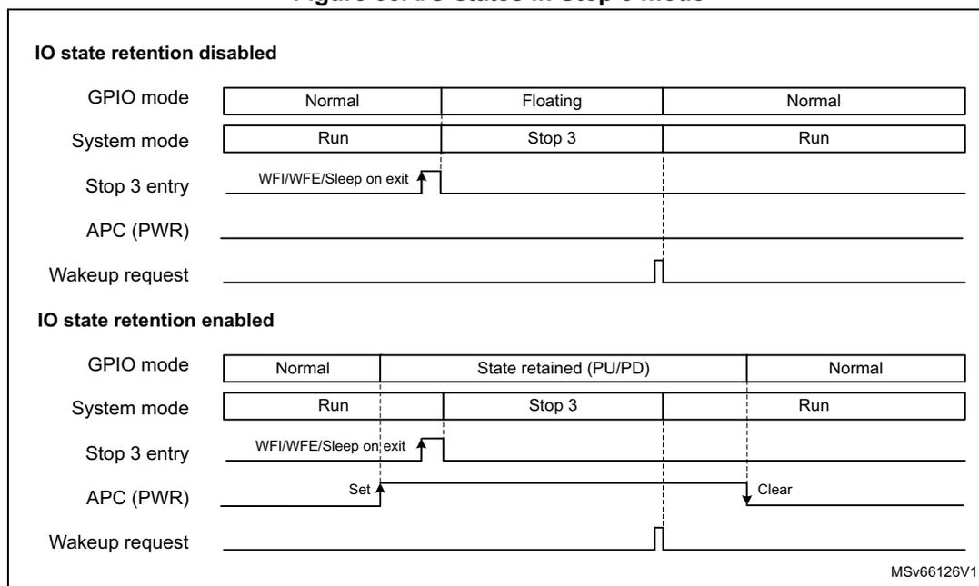
The diagram illustrates the timing of I/O states and system modes during Stop 3 mode entry and exit. It is divided into two sections: 'IO state retention disabled' and 'IO state retention enabled'.
IO state retention disabled:
- GPIO mode: The sequence is Normal → Floating → Normal.
- System mode: The sequence is Run → Stop 3 → Run.
- Stop 3 entry: Triggered by WFI/WFE/Sleep on exit. At this point, the system enters Stop 3 mode and GPIOs become Floating.
- APC (PWR): Remains inactive (low) throughout the sequence.
- Wakeup request: A pulse occurs while in Stop 3 mode, triggering the exit back to Run mode.
IO state retention enabled:
- GPIO mode: The sequence is Normal → State retained (PU/PD) → Normal.
- System mode: The sequence is Run → Stop 3 → Run.
- Stop 3 entry: Triggered by WFI/WFE/Sleep on exit. The system enters Stop 3 mode, and GPIOs enter a State retained (PU/PD) mode.
- APC (PWR): Is Set (high) at Stop 3 entry and remains high until it is manually Cleared (low) after exiting Stop 3 mode.
- Wakeup request: A pulse occurs while in Stop 3 mode, triggering the exit back to Run mode.
MSv66126V1
When exiting the Stop 3 mode, the MCU is in Run mode, range 4.
Note: Wake-up from Stop 3 mode is no longer possible using EXTI interrupt handler and PWR_S3WU interrupt must be enabled.
Table 105. Stop 3 mode
| Stop 3 mode | Description |
|---|---|
| Mode entry | WFI (wait for interrupt) or WFE (wait for event) while:
On Return from ISR while:
Note: To enter Stop 3 mode, all WUFx, and the RTC/TAMP flags generating wake-up interrupts must be cleared. Otherwise, the Stop 3 mode entry procedure is completed but the Stop 3 is exited immediately after entry. |
| Mode exit | WKUPx pin edge (PWR_S3WU), RTC/TAMP event/interrupt, NRST pin external reset, IWDG reset, BOR reset |
| Wake-up latency | Longest wake-up time between: MSIS or HSI16 wake-up time and regulator wake-up time from low-power mode + FLASH wake-up time from Stop 3 mode. |
10.7.10 Standby mode
The lowest power mode in which the BOR is active is the Standby mode. It is based on the Cortex-M33 Deep sleep mode, with the voltage regulators disabled (except when SRAM2 content is preserved). The PLL, HSI16, MSIS, MSIK and HSE oscillators are also switched off.
The SRAMs and register contents are lost except for registers in the backup domain and Standby circuitry (see Figure 32 ). SRAM2 content can be partially or fully preserved depending on RRSB1 and RRSB2 bits configuration in PWR_CR1. In this case, the low-power regulator is ON and provides the supply to SRAM2 only.
The BOR is always available in Standby mode. ULPMEN in PWR_CR1 must be configured to 1 to reach the lowest power consumption by forcing the BOR in ultra-low-power mode (only available when BOR level 0 is selected).
I/O states in Standby mode
In the Standby mode, the I/Os are by default in floating state. If APC bit is set in PWR_APCR, the I/Os can be configured either with a pull-up (see PWR_PUCRx), or with a pull-down (see PWR_PDCRx), or can be kept in analog state if none of the PWR_PUCRx or PWR_PDCRx register is set. The pull-down configuration has highest priority over pull-up configuration in case both PWR_PUCRx and PWR_PDCRx are set for the same I/O. After wake-up from Standby mode, the pull-up/pull-down I/O configuration remains retained based on PWR_PUCRx/PWR_PDCRx registers as long as the APC bit is set.
Some I/Os (listed in Section 13: General-purpose I/Os (GPIO) ) are used for JTAG/SW debug and can only be configured to their respective reset pull-up or pull-down state during
Standby mode setting their respective bit to 1 in the PWR_PUCRx or PWR_PDCRx registers, or to be configured to floating state if the bit is kept at 0.
The RTC outputs on PC13 and PB2 are functional in Standby mode. PC14 and PC15 used for LSE are also functional. The 24 wake-up pins multiplexed on eight events (WKUPx, x = 1 to 8) and the eight RTC tamper pins are available.
Entering Standby mode
The MCU enters the Standby mode as described in Entering into a low-power mode , when the SLEEPDEEP bit in the Cortex-M33 system control register is set (see Table 106 for details on how to enter Standby mode).
In Standby mode, the following features can be selected by programming individual control bits:
- • The independent watchdog (IWDG) is started by writing to its Key register or by hardware option. Once started it cannot be stopped except by a reset (see Section 61.4: IWDG functional description ).
- • The real-time clock (RTC) and Tamper (TAMP) kernel clock enabled by the RTCEN bit in RCC_BDCR.
- • The internal RC oscillator LSI clock or LSI clock divided by 128, is configured by the LSION and LSIPRE bits in RCC_BDCR.
- • The external 32.768 kHz oscillator (LSE) is configured by the LSEON bit in RCC_BDCR.
Exiting Standby mode
The MCU exits the Standby mode as described in Exiting a low-power mode . The SBF status flag in PWR status register (PWR_SR) indicates that the MCU was in Standby mode. All registers are reset after wake-up from Standby except for PWR control register 3 (PWR_CR3) (see Table 106 for more details on how to exit Standby mode).
When exiting Standby mode, I/Os that were configured with pull-up or pull-down during Standby through PWR_PUCRx or PWR_PDCRx, keep this configuration upon exiting Standby mode until the APC bit in PWR_CR3 is cleared by software. The application can release the retained I/O state (clear the retained pull-up/pull-down) by clearing the APC bit after reconfiguring the GPIOs and related peripherals. Once APC is cleared, the I/Os state is configured according to GPIOx registers. The content of the PWR_PUCRx or PWR_PDCRx registers is not lost and can be re-used for a sub-sequent entering into Standby mode.
Some I/Os (listed in Section 13: General-purpose I/Os (GPIO) ) are used for JTAG/SW debug and have internal pull-up or pull-down activated after reset so is configured at this reset value, as well when exiting Standby mode.
For I/Os, with a pull-up or pull-down pre-defined after reset (some JTAG/SW I/Os) or with the GPIOx_PUPDR programming done after exiting from Standby, in case those programming is different from the PWR_PUCRx or PWR_PDCRx programmed value during Standby, both a pull-down and pull-up are applied until APC is cleared, releasing the PWR_PUCRx or PWR_PDCRx programmed value.
Figure 36. I/O states in Standby mode
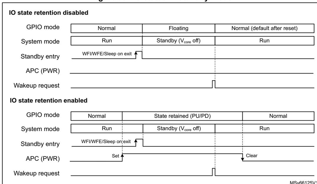
IO state retention disabled
| GPIO mode | Normal | Floating | Normal (default after reset) |
| System mode | Run | Standby ( \( V_{core} \) off) | Run |
| Standby entry | WFI/WFE/Sleep on exit | ||
| APC (PWR) | |||
| Wakeup request | |||
IO state retention enabled
| GPIO mode | Normal | State retained (PU/PD) | Normal |
| System mode | Run | Standby ( \( V_{core} \) off) | Run |
| Standby entry | WFI/WFE/Sleep on exit | ||
| APC (PWR) | Set | Clear | |
| Wakeup request | |||
MSV66125V1
Table 106. Standby mode
| Standby mode | Description |
|---|---|
| Mode entry | WFI (wait for interrupt) or WFE (wait for event) while:
|
| Mode exit | WKUPx pin edge, RTC/TAMP event/interrupt, NRST pin external reset, IWDG reset, BOR reset |
| Wake-up latency | Reset phase |
1. The Standby mode is also entered if LPMS = 11X in PWR_CR1 with BREN = 1 in PWR_BDCR1.
10.7.11 Shutdown mode
The lowest power consumption is reached in Shutdown mode. It is based on the DeepSleep mode with the voltage regulator disabled. The core domain is consequently powered off. The PLL, HSI16, MSIS, MSIK and HSE oscillators are also switched off.
The SRAMs and register contents are lost except for registers in the backup domain. The BOR is not available in Shutdown mode. No power voltage monitoring is possible in this mode, therefore the switch to backup domain is not supported: VBAT mode is not
supported, i.e the RTC, and TAMP are not functional, and the backup SRAM content is not guaranteed if \( V_{DD} \) is powered off during Shutdown mode.
I/O states in Shutdown mode
In the Shutdown mode, I/Os are by default in floating state. If the APC bit in the PWR_APCR register is set, the I/Os can be configured either with a pull-up (see PWR_PUCRx registers ( \( x = A \) to \( J \) )), or with a pull-down (see PWR_PDCRx registers ( \( x = A \) to \( J \) )), or can be kept in analog state if none of PWR_PUCRx or PWR_PDCRx register is set. The pull-down configuration has highest priority over pull-up configuration in case both PWR_PUCRx and PWR_PDCRx are set for the same I/O. However this configuration is lost when exiting the Shutdown mode due to the power-on reset.
Some I/Os (listed in Section 13: General-purpose I/Os (GPIO) ) are used for JTAG/SW debug and can only be configured to their respective reset pull-up or pull-down state during Shutdown mode setting to 1 their respective bit in the PWR_PUCRx or PWR_PDCRx registers, or to be configured to floating state if the bit is kept at 0.
The RTC outputs on PC13 and PB2 are functional in Shutdown mode. PC14 and PC15 used for LSE are also functional. The 24 wake-up pins multiplexed on eight events (WKUPx, \( x = 1 \) to \( 8 \) ) and the eight RTC tampers pins are available.
Entering Shutdown mode
The MCU enters the Shutdown mode as described in Entering into a low-power mode , when the SLEEPDEEP bit in the Cortex-M33 system control register is set (see Table 107 for details on how to enter Shutdown mode).
In Shutdown mode, the following features can be selected by programming individual control bits:
- • The real-time clock (RTC) and Tamper (TAMP) kernel clock enabled by the RTCEN bit in the backup domain control register (RCC_BDCR). Caution: in case of \( V_{DD} \) power-down, the RTC content is lost.
- • The external 32.768 kHz oscillator (LSE) is configured by the LSEON bit in the backup domain control register (RCC_BDCR).
Caution: The Shutdown mode cannot be entered if the BREN bit is set in the PWR backup domain control register 1 (PWR_BDCR1) . If BREN = 1, the Standby mode is entered instead of Shutdown mode.
Exiting Shutdown mode
The MCU exits the Shutdown mode as described in Exiting a low-power mode . A power-on reset occurs when exiting from Shutdown mode. All registers (except for the ones in the backup domain) are reset after a wake-up from Shutdown (see Table 107 for more details on how to exit Shutdown mode).
When exiting Shutdown mode, I/Os that were configured with pull-up or pull-down during Shutdown through registers PWR_PUCRx or PWR_PDCRx lose their configuration and are configured in floating state or to their pull-up pull-down reset value (for some I/Os listed in Section 13: General-purpose I/Os (GPIO) ).
Table 107. Shutdown mode
| Shutdown mode | Description |
|---|---|
| Mode entry | WFI (wait for interrupt) or WFE (wait for event) while:
|
| Mode exit | WKUPx pin edge, RTC/TAMP event/interrupt, NRST pin external reset |
| Wake-up latency | Reset phase |
10.7.12 USB power management in low-power modes (STM32U59x/5Ax/5Fx/5Gx only)
In Stop 0 and Stop 1 modes, it is possible to keep the OTG_HS configuration by leaving the USBPWREN bit set. This allows the OTG_HS to wake up the MCU from Stop mode. However, in order to decrease the power consumption, it is recommended to shut off the OTG_HS before entering Stop 0 or Stop 1 mode.
In Stop 2 and Stop 3 modes, it is not possible to keep the OTG_HS configuration. The OTG_HS must be shut off before entering Stop 2 or Stop 3 mode.
The following steps are needed to shut off the OTG_HS before entering Stop mode:
- 1. Clear USBPWREN and USBBOOSTEN bits in PWR_VOSR.
- 2. Request entry in Stop mode.
Upon wake-up from Stop mode, and before configuring the OTG_HS:
- 1. Make sure the voltage scaling is in range 1 or in range 2 (using VOS[1:0] in PWR_VOSR).
- 2. Make sure the EPOD booster clock is enabled (using PLL1MBOOST[3:0] in RCC_PLL1CFGR)
- 3. Enable the USB internal power by setting USBPWREN and USBBOOSTEN bits in PWR_VOSR.
- 4. Wait for USBBOOSTRDY in PWR_VOSR to be set.
Using PA11 and PA12 GPIOs
When PA11 and PA12 are used as OTG_HS_DM and OTG_HS_DP additional functions, GPIOs must be configured in analog mode (default setting).
When PA11 and PA12 are used as standard GPIOs, set first the USV bit in the PWR_SVMCR register, then the USBPWREN and VDD11USBDIS bits in the PWR_VOSR register must be set prior to configure the GPIOs in a mode other than analog.
In Stop 2, Stop 3, and Standby modes, it is possible to use PA11 and PA12 as standard GPIOs or alternate functions. However, when entering the Stop 2, Stop 3 and Standby low power modes, the OTG_HS PHY power is switched off by hardware and PA11 (driven by OTG_HS_DM) and PA12 (driven by OTG_HS_DP) are strongly pulled-down. Setting the FORCE_USBPWR bit in PWR_CR1 maintain the OTG_HS PHY supply and allows to use PA11 and PA12 as GPIOs.
Note: Setting the FORCE_USBPWR bit induces an extra consumption (typically 50 µA when VDD11USBDIS is set) in Stop 2, Stop 3, and Standby modes. If this is not acceptable, then FORCE_USBPWR bit must remain cleared and in this case, PA11 and PA12 must be kept at low level during Stop 2, Stop 3, and Standby modes.
10.7.13 Power modes output pins
In order to help the debug, three signals are available as device pins alternate functions:
- CSLEEP
When set, CSLEEP indicates that the CPU is in Sleep mode: WFI or WFE has been executed. When cleared, CSLEEP indicates that the CPU is in Run mode.
- CDSTOP
When set, CDSTOP indicates that the CPU domain (CD) is in CStop mode, meaning that the following conditions are filled:
- – WFI or WFE has been executed with CPU SLEEPDEEP = 1.
- – No AHB/APB clock is running in the CPU domain.
When cleared, CDSTOP indicates that the CPU domain is not in CStop mode: AHB/APB clocks run in the CPU domain.
- SRDSTOP
When set, SRDSTOP indicates that the SmartRun domain (SRD) is in DStop mode, meaning that the following conditions are filled:
- – WFI or WFE has been executed with CPU SLEEPDEEP = 1.
- – No AHB/APB clock is running in the SRD domain.
When cleared, SRDSTOP indicates that the SmartRun domain is not in DStop mode: AHB/APB clocks run in the SRD domain.
Note: The AHB/APB clocks run after WFI or WFE has been executed if an autonomous peripheral requests its bus clock in Stop mode. The peripherals bus clock request can delay or prevent the device to enter low-power modes (refer to Section 10.7.2 and Section 10.7.4 ).
The table below explains the MCU power mode depending on these signals states.
Table 108. Power modes output states versus MCU power modes
| CSLEEP | CDSTOP | SRDSTOP | MCU power modes (1) |
|---|---|---|---|
| 0 | 0 | 0 | Run mode |
| 1 | 0 | 0 | Sleep mode or Stop 0 or Stop 1 mode, with AHB/APB clocks running in CPU domain (CD) and SmartRun domain (SRD) |
| 1 | 1 | 0 | Stop 0, Stop 1 or Stop 2 mode, with AHB/APB clocks running in SmartRun domain (SRD) |
| 1 | 1 | 1 | Stop 0, Stop 1, or Stop 2 mode |
- 1. CSLEEP, CDSTOP, and SRDSTOP are generated in core domain, consequently they are not driven in Stop 3, Standby, and Shutdown modes.
10.8 PWR security and privileged protection
10.8.1 PWR security protection
When the TrustZone security is activated by TZEN in FLASH_OPTR, some PWR register fields can be secured against nonsecure access.
The PWR TrustZone security allows the following features to be secured through PWR_SECCFGR:
- • low-power mode
- • wake-up (WKUP) pins
- • voltage detection and monitoring
- • V BAT mode
- • I/O pull-up/pull-down configuration
Other PWR configuration bits are secure when:
- • The system clock selection is secure in RCC: the voltage scaling (VOS) configuration and the regulator booster (BOOSTEN) are secure.
- • A GPIO is configured as secure: its corresponding bit for pull-up/pull-down configuration in Standby mode is secure.
- • The UCPD1 is secure in the GTZC: the PWR_UCPDR register is secure.
Table 109 gives a summary of the PWR secured bits following the security configuration bit in PWR_SECCFGR. As soon as at least one function is configured to be secure, the PWR clock control is also secure in the RCC.
A nonsecure access to a secure-protected register bit is denied:
- • The secured bits are not written (WI) with a nonsecure write access.
- • The secured bits are read as 0 (RAZ) with a nonsecure read access.
A nonsecure write access to PWR_SECCFGR is WI and generates an illegal access event and an interrupt if enabled in the GTZC. It can be read with a nonsecure read access.
When the TrustZone security is disabled (TZEN = 0), PWR_SECCFGR is RAZ/WI, and all other registers are nonsecure.
Table 109. PWR Security configuration summary
| Secure configuration register | Security configuration bit | Register name | Secured bits | Nonsecure access on secure bits |
|---|---|---|---|---|
| PWR_SECCFGR | Not applicable (1) | PWR_SECCFGR | All bits | Read OK. WI and illegal access event |
| PWR_SECCFGR | At least one bit is set | PWR_PRIVCFGR | SPRIV | Read OK. WI |
Table 109. PWR Security configuration summary (continued)
| Secure configuration register | Security configuration bit | Register name | Secured bits | Nonsecure access on secure bits |
|---|---|---|---|---|
| PWR_SECCFGR | LPMSEC | PWR_CR1 | All bits | RAZ/WI |
| PWR_CR2 | All bits | |||
| PWR_SR | CSSF | WI | ||
| PWR_SECCFGR | VDMSEC | PWR_CR3 | All bits | RAZ/WI |
| PWR_SVMCR | All bits | RAZ/WI | ||
| PWR_SECCFGR | VBSEC | PWR_BDCR1 | All bits | RAZ/WI |
| PWR_BDCR2 | All bits | RAZ/WI | ||
| PWR_DBPR | All bits | RAZ/WI | ||
| PWR_SECCFGR | APCSEC | PWR_APCR | All bits | RAZ/WI |
| PWR_SECCFGR | WUPxSEC (x = 1 to 8) | PWR_WUCR1 | WUPENx | RAZ/WI |
| PWR_WUCR2 | WUPPx | RAZ/WI | ||
| PWR_WUCR3 | WUSELx | RAZ/WI | ||
| PWR_WUSCR | CWUFX | WI | ||
| GTZC_TZSC_SECCFGR | UCPD1SEC | PWR_UCPDR | All bits | RAZ/WI |
| RCC_SECCFGR | SYSCLKSEC | PWR_VOSR | VOS[1:0], BOOSTEN, USBPWREN, USBBOOSTEN (2) | RAZ/WI |
| GPIOx_SECCFGR (x=A,B..J) | SECy (y=0..15) | PWR_PUCRx (x = A to J) | PUy (y = 0 to 15) | RAZ/WI |
| PWR_PDCRx (x = A to J) | PDy (y = 0 to 15) | RAZ/WI |
1. PWR_SECCFGR is always secure.
2. USBPWREN and USBBOOSTEN are available in STM32U59x/5Ax/5Fx/5Gx only.
10.8.2 WR privileged protection
By default, after a reset, all PWR registers can be read or written with both privileged and unprivileged accesses, except PWR_PRIVCFGR that can be written with privileged access only. PWR_PRIVCFGR can be read by secure and nonsecure, privileged and unprivileged accesses.
SPRIV in PWR_PRIVCFGR can be written with secure privileged access only. This bit configures the privileged access of all PWR secure functions (defined by PWR_SECCFGR, GTZC, RCC or GPIO as shown in Table 109 ).
When SPRIV is set in PWR_PRIVCFGR:
- • The PWR secure bits can be written only with privileged access, including PWR_SECCFGR.
- • The PWR secure bits can be read only with privileged access except PWR_SECCFGR and PWR_PRIVCFGR that can be read by privileged or unprivileged access.
- • An unprivileged access to a privileged PWR bit or register is discarded: the bits are read as zero and the write to these bits is ignored (RAZ/WI).
NSPRIV in PWR_PRIVCFGR can be written with privileged access only, secure or nonsecure. This bit configures the privileged access of all PWR securable functions that are configured as nonsecure (defined by PWR_SECCFGR, GTZC, RCC or GPIO as shown in Table 109 ).
When NSPRIV is set in PWR_PRIVCFGR:
- • The PWR securable bits that are configured as nonsecure, can be written only with privileged access.
- • The PWR securable bits that are configured as nonsecure, can be read only with privileged access except PWR_PRIVCFGR that can be read by privileged or unprivileged accesses.
- • The VOSRDY and BOOSTRDY bits in PWR_VOSR, PWR_SR, PWR_SVMSR, PWR_BDSR and PWR_WUSR, can be read with privileged or unprivileged accesses.
- • An unprivileged access to a privileged PWR bit or register is discarded: the bits are read as zero and the write to these bits is ignored (RAZ/WI).
10.9 PWR interrupts
The table below gives a summary of the interrupt sources and the way to control them.
Table 110. PWR interrupt requests
| Interrupt vector | Interrupt event | Event flag | Enable control bit | Interrupt clear method | Exit Sleep, Stop 0, 1, 2 modes | Exit Stop 3, Standby, Shutdown modes |
|---|---|---|---|---|---|---|
| PWR_S3WU (1) | wake-up interrupt flag | WUFX (x = 1 to 8) | WUPENx (x = 1 to 8) | Write CWUFX = 1 (x = 1 to 8) | No | Yes (2) |
| PVD_PVM | Programmable voltage detector through EXTI line 16 | PVDO | EXTI line 16 enabled | Write EXTI PIF16 = 1 | Yes | No |
| USB supply voltage monitor through EXTI line 19 | VDDUSBRDY | EXTI line 19 enabled | Write EXTI PIF19 = 1 | Yes | No | |
| V DIO2 supply voltage monitor through EXTI line 20 | VDDIO2RDY | EXTI line 20 enabled | Write EXTI PIF20 = 1 | |||
| Analog supply voltage monitor1 through EXTI line 21 | VDDA1RDY | EXTI line 21 enabled | Write EXTI PIF21 = 1 | |||
| Analog supply voltage monitor2 through EXTI line 22 | VDDA2RDY | EXTI line 22 enabled | Write EXTI PIF22 = 1 |
- 1. The PWR_S3WU interrupt is generated only when STOP3 mode is selected (LPMS = 011 in PWR_CR1 register, not applicable in Stop 0, Stop 1, and Stop 2 modes).
- 2. Only an interrupt can wake up from Stop 3 mode (not possible with an event).
10.10 PWR registers
10.10.1 PWR control register 1 (PWR_CR1)
Address offset: 0x00
Reset value: 0x0000 0000
The register is not affected when exiting Standby mode.
This register is protected against nonsecure access when LPMSEC = 1 in PWR_SECCFGR. This register is protected against unprivileged access when LPMSEC = 1 and SPRIV = 1 in PWR_PRIVCFGR, or when LPMSEC = 0 and NSPRIV = 1.
Access: 14 AHB clock cycles added compared to a standard AHB access
| 31 | 30 | 29 | 28 | 27 | 26 | 25 | 24 | 23 | 22 | 21 | 20 | 19 | 18 | 17 | 16 |
|---|---|---|---|---|---|---|---|---|---|---|---|---|---|---|---|
| Res. | Res. | Res. | Res. | Res. | Res. | Res. | Res. | Res. | Res. | Res. | Res. | Res. | Res. | Res. | Res. |
| 15 | 14 | 13 | 12 | 11 | 10 | 9 | 8 | 7 | 6 | 5 | 4 | 3 | 2 | 1 | 0 |
| FORCE _USBP _WR | Res. | SRAM6 PD | SRAM5 PD | SRAM4 PD | SRAM3 PD | SRAM2 PD | SRAM1 PD | ULPME N | RRSB2 | RRSB1 | Res. | Res. | LPMS[2:0] | ||
| rw | rw | rw | rw | rw | rw | rw | rw | rw | rw | rw | rw | rw | |||
Bits 31:16 Reserved, must be kept at reset value.
Bit 15 FORCE_USBPWR : OTG_HS PHY power maintained during Stop 2, Stop 3, and Standby low-power modes.
0: OTG_HS PHY power is not maintained during low-power modes.
1: OTG_HS PHY power is maintained during low-power modes.
Note: This bit is only available on some devices in the STM32U5 Series. Refer to the device datasheet for availability of its associated peripheral. If not present, consider this bit reserved and keep it at reset value.
Bit 14 Reserved, must be kept at reset value.
Bit 13 SRAM6PD : SRAM6 power down
This bit is used to reduce the consumption by powering off the SRAM6.
0: SRAM6 powered on
1: SRAM6 powered off
Note: This bit is only available on some devices in the STM32U5 Series. Refer to the device datasheet for availability of its associated peripheral. If not present, consider this bit reserved and keep it at reset value.
Bit 12 SRAM5PD : SRAM5 power downThis bit is used to reduce the consumption by powering off the SRAM5.
0: SRAM5 powered on
1: SRAM5 powered off
Note: This bit is only available on some devices in the STM32U5 Series. Refer to the device datasheet for availability of its associated peripheral. If not present, consider this bit reserved and keep it at reset value.
Bit 11 SRAM4PD : SRAM4 power downThis bit is used to reduce the consumption by powering off the SRAM4.
0: SRAM4 powered on
1: SRAM4 powered off
Bit 10 SRAM3PD : SRAM3 power downThis bit is used to reduce the consumption by powering off the SRAM3.
0: SRAM3 powered on
1: SRAM3 powered off
Note: This bit is only available on some devices in the STM32U5 Series. Refer to the device datasheet for availability of its associated peripheral. If not present, consider this bit reserved and keep it at reset value.
Bit 9 SRAM2PD : SRAM2 power downThis bit is used to reduce the consumption by powering off the SRAM2.
0: SRAM2 powered on
1: SRAM2 powered off
Bit 8 SRAM1PD : SRAM1 power downThis bit is used to reduce the consumption by powering off the SRAM1.
0: SRAM1 powered on
1: SRAM1 powered off
Bit 7 ULPMEN : BOR0 ultra-low power modeThis bit is used to reduce the consumption by configuring the BOR in discontinuous mode.
This bit has effect only when the BOR level 0 is selected and when the device is in Standby mode.
0: BOR level 0 operating in continuous (normal) mode in Standby mode
1: BOR level 0 operating in discontinuous (ultra-low power) mode in Standby mode
Caution: This bit must be set to reach the lowest power consumption in Standby mode.
Bit 6 RRSB2 : SRAM2 page 2 retention in Stop 3 and Standby modesThis bit is used to keep the SRAM2 page 2 content in Stop 3 and Standby modes.
The SRAM2 page 2 corresponds to the last 56 Kbytes of the SRAM2 (from SRAM2 base address + 0x2000 to SRAM2 base address + 0xFFFF).
0: SRAM2 page2 content not retained in Stop3 and Standby modes
1: SRAM2 page2 content retained in Stop 3 and Standby modes
Note: This bit has no effect in Shutdown mode.
The backup SRAM is also retained when this bit is set.
Bit 5 RRSB1 : SRAM2 page 1 retention in Stop 3 and Standby modes
This bit is used to keep the SRAM2 page 1 content in Stop 3 and Standby modes. The SRAM2 page 1 corresponds to the first 8 Kbytes of the SRAM2 (from SRAM2 base address to SRAM2 base address + 0x1FFF).
0: SRAM2 page1 content not retained in Stop 3 and Standby modes
1: SRAM2 page1 content retained in Stop 3 and Standby modes
Note: This bit has no effect in Shutdown mode.
The backup SRAM is also retained when this bit is set.
Bits 4:3 Reserved, must be kept at reset value.
Bits 2:0 LPMS[2:0] : Low-power mode selection
These bits select the low-power mode entered when the CPU enters DeepSleep mode.
000: Stop 0 mode
001: Stop 1 mode
010: Stop 2 mode
011: Stop 3 mode
10x: Standby mode (Standby mode also entered if LPMS = 11X in PWR_CR1 with BREN = 1 in PWR_BDCR1)
11x: Shutdown mode if BREN = 0 in PWR_BDCR1
10.10.2 PWR control register 2 (PWR_CR2)
Address offset: 0x04
Reset value: 0x0000 0000
This register is protected against nonsecure access when LPMSEC = 1 in PWR_SECCFGR. This register is protected against unprivileged access when LPMSEC = 1 and SPRIV = 1 in PWR_PRIVCFGR, or when LPMSEC = 0 and NSPRIV = 1.
| 31 | 30 | 29 | 28 | 27 | 26 | 25 | 24 | 23 | 22 | 21 | 20 | 19 | 18 | 17 | 16 |
|---|---|---|---|---|---|---|---|---|---|---|---|---|---|---|---|
| SRDRUN | Res. | Res. | Res. | Res. | JPEGRAMPDS | DSIRAMPDS | GPRA MPDS | SRAM3 PDS8 | SRAM3 PDS7 | SRAM3 PDS6 | SRAM3 PDS5 | SRAM3 PDS4 | SRAM3 PDS3 | SRAM3 PDS2 | SRAM3 PDS1 |
| rw | rw | rw | rw | rw | rw | rw | rw | rw | rw | rw | rw | ||||
| 15 | 14 | 13 | 12 | 11 | 10 | 9 | 8 | 7 | 6 | 5 | 4 | 3 | 2 | 1 | 0 |
| Res. | FLASH FWU | SRAM4 FWU | PKARA MPDS | PRAM PDS | DMA2DRAMPDS | DC1RAMPDS | ICRAM PDS | DC2RAMPDS | SRAM4 PDS | SRAM2 PDS2 | SRAM2 PDS1 | Res. | SRAM1 PDS3 | SRAM1 PDS2 | SRAM1 PDS1 |
| rw | rw | rw | rw | rw | rw | rw | rw | rw | rw | rw | rw | rw | rw |
Bit 31 SRDRUN : SmartRun domain in Run mode
0: SmartRun domain AHB3 and APB3 clocks disabled by default in Stop 0/1/2 modes
1: SmartRun domain AHB3 and APB3 clocks kept enabled in Stop 0/1/2 modes
Bits 30:27 Reserved, must be kept at reset value.
Bit 26 JPEGRAMPDS : JPEG SRAM power-down in Stop 0/1 modes
JPEG SRAM content is always lost in Stop 2 and Stop 3 modes.
0: JPEG SRAM content retained in Stop 0 and Stop 1 modes
1: JPEG SRAM content lost in Stop 0 and Stop 1 modes
Note: This bit is only available on some devices in the STM32U5 Series. Refer to the device datasheet for availability of its associated peripheral. If not present, consider this bit reserved and keep it at reset value.
Bit 25 DSIRAMPDS : DSI SRAM power-down in Stop 0/1 modes
DSI SRAM content is always lost in Stop 2 and Stop 3 modes.
0: DSI SRAM content retained in Stop 0 and Stop 1 modes
1: DSI SRAM content lost in Stop 0 and Stop 1 modes
Note: This bit is only available on some devices in the STM32U5 Series. Refer to the device datasheet for availability of its associated peripheral. If not present, consider this bit reserved and keep it at reset value.
Bit 24 GPRAMPDS : Graphic peripherals (LTDC, GFXMMU) SRAM power-down in all Stop modes
0: Graphic peripherals SRAM content retained in Stop modes
1: Graphic peripherals SRAM content lost in Stop modes
Note: LTDC SRAM content is always lost in Stop 2 and Stop 3 modes. It can be retained only in Stop 0 and Stop 1 modes.
This bit is only available on some devices in the STM32U5 Series. Refer to the device datasheet for availability of its associated peripheral. If not present, consider this bit reserved and keep it at reset value.
Bit 23 SRAM3PDS8 : SRAM3 page 8 (64 Kbytes) power-down in all Stop modes
0: SRAM3 page 8 content retained in Stop modes
1: SRAM3 page 8 content lost in Stop modes
Note: This bit is only available on some devices in the STM32U5 Series. Refer to the device datasheet for availability of its associated peripheral. If not present, consider this bit reserved and keep it at reset value.
Bit 22 SRAM3PDS7 : SRAM3 page 7 (64 Kbytes) power-down in all Stop modes
0: SRAM3 page 7 content retained in Stop modes
1: SRAM3 page 7 content lost in Stop modes
Note: This bit is only available on some devices in the STM32U5 Series. Refer to the device datasheet for availability of its associated peripheral. If not present, consider this bit reserved and keep it at reset value.
Bit 21 SRAM3PDS6 : SRAM3 page 6 (64 Kbytes) power-down in all Stop modes
0: SRAM3 page 6 content retained in Stop modes
1: SRAM3 page 6 content lost in Stop modes
Note: This bit is only available on some devices in the STM32U5 Series. Refer to the device datasheet for availability of its associated peripheral. If not present, consider this bit reserved and keep it at reset value.
Bit 20 SRAM3PDS5 : SRAM3 page 5 (64 Kbytes) power-down in all Stop modes
0: SRAM3 page 5 content retained in Stop modes
1: SRAM3 page 5 content lost in Stop modes
Note: This bit is only available on some devices in the STM32U5 Series. Refer to the device datasheet for availability of its associated peripheral. If not present, consider this bit reserved and keep it at reset value.
Bit 19 SRAM3PDS4 : SRAM3 page 4 (64 Kbytes) power-down in all Stop modes
0: SRAM3 page 4 content retained in Stop modes
1: SRAM3 page 4 content lost in Stop modes
Note: This bit is only available on some devices in the STM32U5 Series. Refer to the device datasheet for availability of its associated peripheral. If not present, consider this bit reserved and keep it at reset value.
Bit 18 SRAM3PDS3 : SRAM3 page 3 (64 Kbytes) power-down in all Stop modes
0: SRAM3 page 3 content retained in Stop modes
1: SRAM3 page 3 content lost in Stop modes
Note: This bit is only available on some devices in the STM32U5 Series. Refer to the device datasheet for availability of its associated peripheral. If not present, consider this bit reserved and keep it at reset value.
Bit 17 SRAM3PDS2 : SRAM3 page 2 (64 Kbytes) power-down in all Stop modes
0: SRAM3 page 2 content retained in Stop modes
1: SRAM3 page 2 content lost in Stop modes
Note: This bit is only available on some devices in the STM32U5 Series. Refer to the device datasheet for availability of its associated peripheral. If not present, consider this bit reserved and keep it at reset value.
Bit 16 SRAM3PDS1 : SRAM3 page 1 (64 Kbytes) power-down in all Stop modes
0: SRAM3 page 1 content retained in Stop modes
1: SRAM3 page 1 content lost in Stop modes
Note: This bit is only available on some devices in the STM32U5 Series. Refer to the device datasheet for availability of its associated peripheral. If not present, consider this bit reserved and keep it at reset value.
Bit 15 Reserved, must be kept at reset value.
Bit 14 FLASHFWU : Flash memory fast wake-up from Stop 0 and Stop 1 modes
This bit is used to obtain the best trade-off between low-power consumption and wake-up time when exiting the Stop 0 or Stop 1 modes.
When this bit is set, the flash memory remains in normal mode in Stop 0 and Stop 1 modes, which offers a faster startup time with higher consumption.
0: Flash memory enters low-power mode in Stop 0/1 modes (lower-power consumption).
1: Flash memory remains in normal mode in Stop 0/1 modes (faster wake-up time).
Bit 13 SRAM4FWU : SRAM4 fast wake-up from Stop 0/1/2 modes
This bit is used to obtain the best trade-off between low-power consumption and wake-up time. SRAM4 wake-up time increases the wake-up time when exiting Stop 0/1/2 modes, and also increases the LPDMA access time to SRAM4 during Stop modes.
0: SRAM4 enters low-power mode in Stop 0/1/2 modes (source biasing for lower-power consumption).
1: SRAM4 remains in normal mode in Stop 0/1/2 modes (higher consumption but no SRAM4 wake-up time).
Bit 12 PKARAMPDS : PKA SRAM power-down in all Stop modes (Stop 0/1/2/3)
0: PKA SRAM content retained in Stop modes
1: PKA SRAM content lost in Stop modes
Note: This bit is only available on some devices in the STM32U5 Series. Refer to the device datasheet for availability of its associated peripheral. If not present, consider this bit reserved and keep at reset value.
Bit 11 PRAMPDS : FMAC, FDCAN, and USB/OTG_FS/OTG_HS SRAM power-down in all Stop modes (Stop 0/1/2/3)
0: FMAC, FDCAN, and USB/OTG_FS/OTG_HS SRAM content retained in Stop modes
1: FMAC, FDCAN, and USB/OTG_FS/OTG_HS SRAM content lost in Stop modes
Bit 10 DMA2DRAMPDS : DMA2D SRAM power-down in all Stop modes
0: DMA2D SRAM content retained in Stop modes
1: DMA2D SRAM content lost in Stop modes
Note: This bit is only available on some devices in the STM32U5 Series. Refer to the device datasheet for availability of its associated peripheral. If not present, consider this bit reserved and keep it at reset value.
Bit 9 DC1RAMPDS : DCACHE1 SRAM power-down in all Stop modes
0: DCACHE1 SRAM content retained in Stop modes
1: DCACHE1 SRAM content lost in Stop modes
Bit 8 ICRAMPDS : ICACHE SRAM power-down in all Stop modes
0: ICACHE SRAM content retained in Stop modes
1: ICACHE SRAM content lost in Stop modes
Bit 7 DC2RAMPDS : DCACHE2 SRAM power-down in all Stop modes
0: DCACHE2 SRAM content retained in Stop modes
1: DCACHE2 SRAM content lost in Stop modes
Note: This bit is only available on some devices in the STM32U5 Series. Refer to the device datasheet for availability of its associated peripheral. If not present, consider this bit reserved and keep it at reset value.
Bit 6 SRAM4PDS : SRAM4 power-down in all Stop modes
0: SRAM4 content retained in Stop modes
1: SRAM4 content lost in Stop modes
Bit 5 SRAM2PDS2 : SRAM2 page 2 (56 Kbytes) power-down in Stop 0/1/2 modes
0: SRAM2 page 2 content retained in Stop modes
1: SRAM2 page 2 content lost in Stop modes
Note: The SRAM2 page 2 retention in Stop 3 is controlled by RRSB2 bit in PWR_CR1.
Bit 4 SRAM2PDS1 : SRAM2 page 1 (8 Kbytes) power-down in Stop 0/1/2 modes
0: SRAM2 page 1 content retained in Stop modes
1: SRAM2 page 1 content lost in Stop modes
Note: The SRAM2 page 1 retention in Stop 3 is controlled by RRSB1 bit in PWR_CR1.
Bit 3 Reserved, must be kept at reset value.
Bit 2 SRAM1PDS3 : SRAM1 page 3 (64 Kbytes) power-down in all Stop modes
0: SRAM1 page 3 content retained in Stop modes
1: SRAM1 page 3 content lost in Stop modes
Bit 1 SRAM1PDS2 : SRAM1 page 2 (64 Kbytes) power-down in all Stop modes
0: SRAM1 page 2 content retained in Stop modes
1: SRAM1 page 2 content lost in Stop modes
Bit 0 SRAM1PDS1 : SRAM1 page 1 (64 Kbytes) power-down in all Stop modes
0: SRAM1 page 1 content retained in Stop modes
1: SRAM1 page 1 content lost in Stop modes
10.10.3 PWR control register 3 (PWR_CR3)
Address offset: 0x08
Power-on reset value: 0x0000 0000
Exit from Standby modes: not affected
System reset: not affected, except REGSEL that is cleared to 0
This register is protected against nonsecure access when VDMSEC = 1 in PWR_SECCFGR. This register is protected against unprivileged access when VDMSEC = 1 and SPRIV = 1 in PWR_PRIVCFGR, or when VDMSEC = 0 and NSPRIV = 1.
Access: 14 AHB clock cycles added compared to a standard AHB access.
| 31 | 30 | 29 | 28 | 27 | 26 | 25 | 24 | 23 | 22 | 21 | 20 | 19 | 18 | 17 | 16 |
|---|---|---|---|---|---|---|---|---|---|---|---|---|---|---|---|
| Res. | Res. | Res. | Res. | Res. | Res. | Res. | Res. | Res. | Res. | Res. | Res. | Res. | Res. | Res. | Res. |
| 15 | 14 | 13 | 12 | 11 | 10 | 9 | 8 | 7 | 6 | 5 | 4 | 3 | 2 | 1 | 0 |
| Res. | Res. | Res. | Res. | Res. | Res. | Res. | Res. | Res. | Res. | Res. | Res. | Res. | FSTEN | REGSEL | Res. |
| rw | rw | ||||||||||||||
Bits 31:3 Reserved, must be kept at reset value.
Bit 2
FSTEN
: Fast soft start
0: LDO/SMPS fast startup disabled (limited inrush current)
1: LDO/SMPS fast startup enabled
Bit 1
REGSEL
: Regulator selection
0: LDO selected
1: SMPS selected
Note: REGSEL is reserved and must be kept at reset value in packages without SMPS.
Bit 0 Reserved, must be kept at reset value.
10.10.4 PWR voltage scaling register (PWR_VOSR)
Address offset: 0x0C
Reset value: 0x0000 8000
Some register fields are protected against nonsecure access depending on RCC_SECCFGR. These fields can be protected against unprivileged access depending on PWR_PRIVCFGR.
| 31 | 30 | 29 | 28 | 27 | 26 | 25 | 24 | 23 | 22 | 21 | 20 | 19 | 18 | 17 | 16 |
|---|---|---|---|---|---|---|---|---|---|---|---|---|---|---|---|
| Res. | Res. | Res. | Res. | Res. | Res. | Res. | Res. | Res. | Res. | VDD11 USBDIS | USBBO OSTEN | USBP WREN | BOOST EN | VOS[1:0] | |
| rw | rw | rw | rw | rw | rw | ||||||||||
| 15 | 14 | 13 | 12 | 11 | 10 | 9 | 8 | 7 | 6 | 5 | 4 | 3 | 2 | 1 | 0 |
| VOSR DY | BOOST RDY | USBBO OSTRDY | Res. | Res. | Res. | Res. | Res. | Res. | Res. | Res. | Res. | Res. | Res. | Res. | Res. |
| r | r | r | |||||||||||||
Bits 31:22 Reserved, must be kept at reset value.
Bit 21 VDD11USBDIS : OTG_HS VDD11USB disable
This bit is protected against nonsecure access when SYSCLKSEC = 1 in RCC_SECCFGR.
It is protected against unprivileged access when SYSCLKSEC = 1 in RCC_SECCFGR and SPRIV = 1 in PWR_PRIVCFGGR, or when SYSCLKSEC = 0 and NSPRIV = 1.
0: VDD11USB enabled
1: VDD11USB disabled
Note: This bit is only available on some devices in the STM32U5 Series. Refer to the device datasheet for availability of its associated peripheral. If not present, consider this bit reserved and keep it at reset value.
Bit 20 USBBOOSTEN : OTG_HS EPOD booster enable
This bit is protected against nonsecure access when SYSCLKSEC = 1 in RCC_SECCFGR.
It is protected against unprivileged access when SYSCLKSEC = 1 in RCC_SECCFGR and SPRIV = 1 in PWR_PRIVCFGGR, or when SYSCLKSEC = 0 and NSPRIV = 1.
This bit must be set in range 1 and range 2 before enabling the OTG_HS.
This bit is reset when going in all Stop modes.
0: OTG_HS booster disabled
1: OTG_HS booster enabled
Note: This bit is only available on some devices in the STM32U5 Series. Refer to the device datasheet for availability of its associated peripheral. If not present, consider this bit reserved and keep it at reset value.
Bit 19 USBPWREN : OTG_HS power enable
This bit is protected against nonsecure access when SYSCLKSEC = 1 in RCC_SECCFGR.
It is protected against unprivileged access when SYSCLKSEC = 1 in RCC_SECCFGR and SPRIV = 1 in PWR_PRIVCFGGR, or when SYSCLKSEC = 0 and NSPRIV = 1.
0: OTG_HS power disabled
1: OTG_HS power enabled
Note: This bit is only available on some devices in the STM32U5 Series. Refer to the device datasheet for availability of its associated peripheral. If not present, consider this bit reserved and keep it at reset value.
Bit 18 BOOSTEN : EPOD booster enable
This bit is protected against nonsecure access when SYSCLKSEC = 1 in RCC_SECCFGR.
It is protected against unprivileged access when SYSCLKSEC = 1 in RCC_SECCFGR and SPRIV = 1 in PWR_PRIVCFGGR, or when SYSCLKSEC = 0 and NSPRIV = 1.
This bit must be set in range 1 and range 2 before increasing the system clock frequency above 55 MHz. This bit is reset when going in all Stop modes.
0: Booster disabled
1: Booster enabled
Bits 17:16 VOS[1:0] : Voltage scaling range selection
This field is protected against nonsecure access when SYSCLKSEC = 1 in
RCC_SECCFGR. It is protected against unprivileged access when SYSCLKSEC = 1 in RCC_SECCFGR and SPRIV = 1 in PWR_PRIVCFGGR, or when SYSCLKSEC = 0 and NSPRIV = 1.
00: Range 4 (lowest power)
01: Range 3
10: Range 2
11: Range 1 (highest frequency)
Bit 15 VOSRDY : Ready bit for V CORE voltage scaling output selection
0: Not ready, voltage level < VOS selected level
1: Ready, voltage level ≥ VOS selected level
Bit 14 BOOSTRDY : EPOD booster ready
This bit is set to one by hardware when the power booster startup time is reached.
The system clock frequency can be switched higher than 55 MHz only after this bit is set.
0: Power booster not ready
1: Power booster ready
Bit 13 USBBOOSTRDY : OTG_HS EPOD booster ready
This bit is set to one by hardware when the power booster startup time is reached.
The OTG_HS clock can be provided only after this bit is set.
0: OTG_HS power booster not ready
1: OTG_HS power booster ready
Note: This bit is only available on some devices in the STM32U5 Series. Refer to the device datasheet for availability of its associated peripheral. If not present, consider this bit reserved and keep it at reset value.
Bits 12:0 Reserved, must be kept at reset value.
10.10.5 PWR supply voltage monitoring control register (PWR_SVMCR)
Address offset: 0x10
Reset value: 0x0000 0000
This register is protected against nonsecure access when VDMSEC = 1 in PWR_SECCFGR. This register is protected against unprivileged access when VDMSEC = 1 and SPRIV = 1 in PWR_PRIVCFGR, or when VDMSEC = 0 and NSPRIV = 1.
| 31 | 30 | 29 | 28 | 27 | 26 | 25 | 24 | 23 | 22 | 21 | 20 | 19 | 18 | 17 | 16 |
|---|---|---|---|---|---|---|---|---|---|---|---|---|---|---|---|
| Res. | ASV | IO2SV | USV | AVM2EN | AVM1EN | IO2VMEN | UVMEN | Res. | Res. | Res. | Res. | Res. | Res. | Res. | Res. |
| rw | rw | rw | rw | rw | rw | rw | |||||||||
| 15 | 14 | 13 | 12 | 11 | 10 | 9 | 8 | 7 | 6 | 5 | 4 | 3 | 2 | 1 | 0 |
| Res. | Res. | Res. | Res. | Res. | Res. | Res. | Res. | PVDLS[2:0] | PVDE | Res. | Res. | Res. | Res. | ||
| rw | rw | rw | rw | ||||||||||||
Bit 31 Reserved, must be kept at reset value.
Bit 30 ASV : \( V_{DDA} \) independent analog supply valid
This bit is used to validate the \( V_{DDA} \) supply for electrical and logical isolation purpose.
Setting this bit is mandatory to use the analog peripherals. If \( V_{DDA} \) is not always present in the application, the \( V_{DDA} \) voltage monitor can be used to determine whether this supply is ready or not.
0: \( V_{DDA} \) not present: logical and electrical isolation is applied to ignore this supply.
1: \( V_{DDA} \) valid
Bit 29 IO2SV : \( V_{DDIO2} \) independent I/Os supply valid
This bit is used to validate the \( V_{DDIO2} \) supply for electrical and logical isolation purpose.
Setting this bit is mandatory to use PG[15:2]. If \( V_{DDIO2} \) is not always present in the application, the \( V_{DDIO2} \) voltage monitor can be used to determine whether this supply is ready or not.
0: \( V_{DDIO2} \) not present: logical and electrical isolation is applied to ignore this supply.
1: \( V_{DDIO2} \) valid
Bit 28 USV : \( V_{DDUSB} \) independent USB supply valid
This bit is used to validate the \( V_{DDUSB} \) supply for electrical and logical isolation purpose. Setting this bit is mandatory to use the USB/OTG_FS/OTG_HS. If \( V_{DDUSB} \) is not always present in the application, the \( V_{DDUSB} \) voltage monitor can be used to determine whether this supply is ready or not.
0: \( V_{DDUSB} \) not present: logical and electrical isolation is applied to ignore this supply.
1: \( V_{DDUSB} \) valid
Bit 27 AVM2EN : \( V_{DDA} \) independent analog supply voltage monitor 2 enable (1.8 V threshold)
0: \( V_{DDA} \) voltage monitor 2 disabled
1: \( V_{DDA} \) voltage monitor 2 enabled
Bit 26 AVM1EN : \( V_{DDA} \) independent analog supply voltage monitor 1 enable (1.6 V threshold)
0: \( V_{DDA} \) voltage monitor 1 disabled
1: \( V_{DDA} \) voltage monitor 1 enabled
Bit 25 IO2VMEN : \( V_{DDIO2} \) independent I/Os voltage monitor enable
0: \( V_{DDIO2} \) voltage monitor disabled
1: \( V_{DDIO2} \) voltage monitor enabled
Bit 24 UVMEN : \( V_{DDUSB} \) independent USB voltage monitor enable
0: \( V_{DDUSB} \) voltage monitor disabled
1: \( V_{DDUSB} \) voltage monitor enabled
Bits 23:8 Reserved, must be kept at reset value.
Bits 7:5 PVDLS[2:0] : Programmable voltage detector (PVD) level selection
These bits select the voltage threshold detected by the PVD:
000: \( V_{PVD0} \) around 2.0 V
001: \( V_{PVD1} \) around 2.2 V
010: \( V_{PVD2} \) around 2.4 V
011: \( V_{PVD3} \) around 2.5 V
100: \( V_{PVD4} \) around 2.6 V
101: \( V_{PVD5} \) around 2.8 V
110: \( V_{PVD6} \) around 2.9 V
111: External input analog voltage PVD_IN (compared internally to VREFINT)
Bit 4 PVDE : Programmable voltage detector enable
0: PVD disabled
1: PVD enabled
Bits 3:0 Reserved, must be kept at reset value.
10.10.6 PWR wake-up control register 1 (PWR_WUCR1)
Access: 14 AHB clock cycles added compared to a standard AHB access
Address offset: 0x14
Reset value: 0x0000 0000
The register is not affected when exiting Standby mode.
Each WUPENx (x = 1 to 8) is protected against nonsecure access when WUPxSEC = 1 in PWR_SECCFGR. Each WUPENx is protected against unprivileged access when
WUPxSEC = 1 in PWR_SECCFGR and SPRIV = 1 in PWR_PRIVCFGR, or when
WUPxSEC = 0 and NSPRIV = 1 .
| 31 | 30 | 29 | 28 | 27 | 26 | 25 | 24 | 23 | 22 | 21 | 20 | 19 | 18 | 17 | 16 |
|---|---|---|---|---|---|---|---|---|---|---|---|---|---|---|---|
| Res. | Res. | Res. | Res. | Res. | Res. | Res. | Res. | Res. | Res. | Res. | Res. | Res. | Res. | Res. | Res. |
| 15 | 14 | 13 | 12 | 11 | 10 | 9 | 8 | 7 | 6 | 5 | 4 | 3 | 2 | 1 | 0 |
| Res. | Res. | Res. | Res. | Res. | Res. | Res. | Res. | WUPE N8 | WUPE N7 | WUPE N6 | WUPE N5 | WUPE N4 | WUPE N3 | WUPE N2 | WUPE N1 |
| rw | rw | rw | rw | rw | rw | rw | rw |
Bits 31:8 Reserved, must be kept at reset value.
Bit 7 WUPEN8 : wake-up pin WKUP8 enable
0: WKUP8 disabled
1: WKUP8 enabled
Bit 6 WUPEN7 : wake-up pin WKUP7 enable
0: WKUP7 disabled
1: WKUP7 enabled
Bit 5 WUPEN6 : wake-up pin WKUP6 enable
0: WKUP6 disabled
1: WKUP6 enabled
Bit 4 WUPEN5 : wake-up pin WKUP5 enable
0: WKUP5 disabled
1: WKUP5 enabled
Bit 3 WUPEN4 : wake-up pin WKUP4 enable
0: WKUP4 disabled
1: WKUP4 enabled
Bit 2 WUPEN3 : wake-up pin WKUP3 enable
0: WKUP3 disabled
1: WKUP3 enabled
Bit 1 WUPEN2 : wake-up pin WKUP2 enable
0: WKUP2 disabled
1: WKUP2 enabled
Bit 0 WUPEN1 : wake-up pin WKUP1 enable
0: WKUP1 disabled
1: WKUP1 enabled
10.10.7 PWR wake-up control register 2 (PWR_WUCR2)
Address offset: 0x18
Reset value: 0x0000 0000
The register is not affected when exiting Standby mode.
Each WUPPx (x = 1 to 8) is protected against nonsecure access when WUPxSEC = 1 in PWR_SECCFGR. Each WUPPx is protected against unprivileged access when
WUPxSEC = 1 in PWR_SECCFGR and SPRIV = 1 in PWR_PRIVCFGR, or when WUPxSEC = 0 and NSPRIV = 1.
Access: 14 AHB clock cycles added compared to a standard AHB access
| 31 | 30 | 29 | 28 | 27 | 26 | 25 | 24 | 23 | 22 | 21 | 20 | 19 | 18 | 17 | 16 |
| Res. | Res. | Res. | Res. | Res. | Res. | Res. | Res. | Res. | Res. | Res. | Res. | Res. | Res. | Res. | Res. |
| 15 | 14 | 13 | 12 | 11 | 10 | 9 | 8 | 7 | 6 | 5 | 4 | 3 | 2 | 1 | 0 |
| Res. | Res. | Res. | Res. | Res. | Res. | Res. | Res. | WUPP 8 rw | WUPP 7 rw | WUPP 6 rw | WUPP 5 rw | WUPP 4 rw | WUPP 3 rw | WUPP 2 rw | WUPP 1 rw |
Bits 31:8 Reserved, must be kept at reset value.
Bit 7 WUPP8 : wake-up pin WKUP8 polarity
This bit must be configured when WUPEN8 = 0.
0: Detection on high level (rising edge)
1: Detection on low level (falling edge)
Bit 6 WUPP7 : wake-up pin WKUP7 polarity
This bit must be configured when WUPEN7 = 0.
0: Detection on high level (rising edge)
1: Detection on low level (falling edge)
Bit 5 WUPP6 : wake-up pin WKUP6 polarity
This bit must be configured when WUPEN6 = 0.
0: Detection on high level (rising edge)
1: Detection on low level (falling edge)
Bit 4 WUPP5 : wake-up pin WKUP5 polarity
This bit must be configured when WUPEN5 = 0.
0: Detection on high level (rising edge)
1: Detection on low level (falling edge)
Bit 3 WUPP4 : wake-up pin WKUP4 polarity
This bit must be configured when WUPEN4 = 0.
0: Detection on high level (rising edge)
1: Detection on low level (falling edge)
Bit 2 WUPP3 : wake-up pin WKUP3 polarity
This bit must be configured when WUPEN3 = 0.
0: Detection on high level (rising edge)
1: Detection on low level (falling edge)
Bit 1 WUPP2 : wake-up pin WKUP2 polarity
This bit must be configured when WUPEN2 = 0.
0: Detection on high level (rising edge)
1: Detection on low level (falling edge)
Bit 0 WUPP1 : wake-up pin WKUP1 polarity.
This bit must be configured when WUPEN1 = 0.
0: Detection on high level (rising edge)
1: Detection on low level (falling edge)
10.10.8 PWR wake-up control register 3 (PWR_WUCR3)
Address offset: 0x1C
Reset value: 0x0000 0000
The register is not affected when exiting Standby mode.
Each WUSELx (x = 1 to 8) is protected against nonsecure access when WUPxSEC = 1 in PWR_SECCFGR. Each WUSELx is protected against unprivileged access when WUPxSEC = 1 in PWR_SECCFGR and SPRIV = 1 in PWR_PRIVCFGR, or when WUPxSEC = 0 and NSPRIV = 1.
Access: 14 AHB clock cycles added compared to a standard AHB access
| 31 | 30 | 29 | 28 | 27 | 26 | 25 | 24 | 23 | 22 | 21 | 20 | 19 | 18 | 17 | 16 |
|---|---|---|---|---|---|---|---|---|---|---|---|---|---|---|---|
| Res | Res | Res | Res | Res | Res | Res | Res | Res | Res | Res | Res | Res | Res | Res | Res |
| 15 | 14 | 13 | 12 | 11 | 10 | 9 | 8 | 7 | 6 | 5 | 4 | 3 | 2 | 1 | 0 |
| WUSEL8[1:0] | WUSEL7[1:0] | WUSEL6[1:0] | WUSEL5[1:0] | WUSEL4[1:0] | WUSEL3[1:0] | WUSEL2[1:0] | WUSEL1[1:0] | ||||||||
| rw | rw | rw | rw | rw | rw | rw | rw | rw | rw | rw | rw | rw | rw | rw | rw |
Bits 31:16 Reserved, must be kept at reset value.
Bits 15:14 WUSEL8[1:0] : wake-up pin WKUP8 selection
This field must be configured when WUPEN8 = 0.
00: WKUP8_0
01: WKUP8_1
10: WKUP8_2
11: WKUP8_3
Bits 13:12 WUSEL7[1:0] : wake-up pin WKUP7 selection
This field must be configured when WUPEN7 = 0.
00: WKUP7_0
01: WKUP7_1
10: WKUP7_2
11: WKUP7_3
Bits 11:10 WUSEL6[1:0] : wake-up pin WKUP6 selection
This field must be configured when WUPEN6 = 0.
00: WKUP6_0
01: WKUP6_1
10: WKUP6_2
11: WKUP6_3
Bits 9:8 WUSEL5[1:0] : wake-up pin WKUP5 selection
This field must be configured when WUPEN5 = 0.
00: WKUP5_0
01: WKUP5_1
10: WKUP5_2
11: WKUP5_3
Bits 7:6 WUSEL4[1:0] : wake-up pin WKUP4 selection
This field must be configured when WUPEN4 = 0.
00: WKUP4_0
01: WKUP4_1
10: WKUP4_2
11: WKUP4_3
Bits 5:4 WUSEL3[1:0] : wake-up pin WKUP3 selection
This field must be configured when WUPEN3 = 0.
00: WKUP3_0
01: WKUP3_1
10: WKUP3_2
11: WKUP3_3
Bits 3:2 WUSEL2[1:0] : wake-up pin WKUP2 selection
This field must be configured when WUPEN2 = 0.
00: WKUP2_0
01: WKUP2_1
10: WKUP2_2
11: WKUP2_3
Bits 1:0 WUSEL1[1:0] : wake-up pin WKUP1 selection
This field must be configured when WUPEN1 = 0.
00: WKUP0_0
01: WKUP0_1
10: WKUP0_2
11: WKUP0_3
10.10.9 PWR backup domain control register 1 (PWR_BDCR1)
Address offset: 0x20
Backup domain reset value: 0x0000 0000
Power-on reset: not affected
The register is not affected when exiting Standby mode.
System reset: not affected
This register is write-protected when DBP is cleared in PWR_DBPR. This register is protected against nonsecure access when VBSEC = 1 in PWR_SECCFGR. This register is protected against unprivileged access when VBSEC = 1 and SPRIV = 1 in PWR_PRIVCFGR, or when VBSEC = 0 and NSPRIV = 1.
Access: 14 AHB clock cycles added compared to a standard AHB access
| 31 | 30 | 29 | 28 | 27 | 26 | 25 | 24 | 23 | 22 | 21 | 20 | 19 | 18 | 17 | 16 |
|---|---|---|---|---|---|---|---|---|---|---|---|---|---|---|---|
| Res. | Res. | Res. | Res. | Res. | Res. | Res. | Res. | Res. | Res. | Res. | Res. | Res. | Res. | Res. | Res. |
| 15 | 14 | 13 | 12 | 11 | 10 | 9 | 8 | 7 | 6 | 5 | 4 | 3 | 2 | 1 | 0 |
| Res. | Res. | Res. | Res. | Res. | Res. | Res. | Res. | Res. | Res. | Res. | MONE N | Res. | Res. | Res. | BREN |
| rw | rw |
Bits 31:5 Reserved, must be kept at reset value.
Bit 4 MONEN : Backup domain voltage and temperature monitoring enable
0: Backup domain voltage and temperature monitoring disabled
1: Backup domain voltage and temperature monitoring enabled
Bits 3:1 Reserved, must be kept at reset value.
Bit 0 BREN : Backup RAM retention in Standby and \( V_{BAT} \) modes
When this bit is set, the backup RAM content is kept in Standby (1) and \( V_{BAT} \) modes.
If BREN is reset, the backup RAM can still be used in Run, Sleep, and Stop modes. However, its content is lost in Standby, Shutdown, and \( V_{BAT} \) modes. This bit can be written only when the regulator is LDO, which must be configured before switching to SMPS.
0: Backup RAM content lost in Standby (1) and \( V_{BAT} \) modes
1: Backup RAM content preserved in Standby and \( V_{BAT} \) modes
Note: Backup RAM cannot be preserved in Shutdown mode.
- 1. The backup SRAM content is lost in Standby mode without SRAM2 retention. If either RRSB1 or RRSB2 bit is set in Standby mode, the backup SRAM is also retained.
10.10.10 PWR backup domain control register 2 (PWR_BDCR2)
Address offset: 0x24
Power-on reset value: 0x0000 0000
The register is not affected when exiting Standby mode.
System reset: not affected
This register is protected against nonsecure access when VBSEC = 1 in PWR_SECCFGR.
This register is protected against unprivileged access when VBSEC = 1 and SPRIV = 1 in PWR_PRIVCFGR, or when VBSEC = 0 and NSPRIV = 1.
Access: 14 AHB clock cycles added compared to a standard AHB access
| 31 | 30 | 29 | 28 | 27 | 26 | 25 | 24 | 23 | 22 | 21 | 20 | 19 | 18 | 17 | 16 |
|---|---|---|---|---|---|---|---|---|---|---|---|---|---|---|---|
| Res. | Res. | Res. | Res. | Res. | Res. | Res. | Res. | Res. | Res. | Res. | Res. | Res. | Res. | Res. | Res. |
| 15 | 14 | 13 | 12 | 11 | 10 | 9 | 8 | 7 | 6 | 5 | 4 | 3 | 2 | 1 | 0 |
| Res. | Res. | Res. | Res. | Res. | Res. | Res. | Res. | Res. | Res. | Res. | Res. | Res. | Res. | VBRS | VBE |
| rw | rw |
Bits 31:2 Reserved, must be kept at reset value.
Bit 1 VBRS : \( V_{BAT} \) charging resistor selection
0: Charge \( V_{BAT} \) through a 5 k \( \Omega \) resistor.
1: Charge \( V_{BAT} \) through a 1.5 k \( \Omega \) resistor.
Bit 0 VBE : \( V_{BAT} \) charging enable
0: \( V_{BAT} \) battery charging disabled
1: \( V_{BAT} \) battery charging enabled
10.10.11 PWR disable backup domain register (PWR_DBPR)
Address offset: 0x28
Reset value: 0x0000 0000
This register is protected against nonsecure access when VBSEC = 1 in PWR_SECCFGR.
This register is protected against unprivileged access when VBSEC = 1 and SPRIV = 1 in PWR_PRIVCFGR, or when VBSEC = 0 and NSPRIV = 1.
| 31 | 30 | 29 | 28 | 27 | 26 | 25 | 24 | 23 | 22 | 21 | 20 | 19 | 18 | 17 | 16 |
|---|---|---|---|---|---|---|---|---|---|---|---|---|---|---|---|
| Res. | Res. | Res. | Res. | Res. | Res. | Res. | Res. | Res. | Res. | Res. | Res. | Res. | Res. | Res. | Res. |
| 15 | 14 | 13 | 12 | 11 | 10 | 9 | 8 | 7 | 6 | 5 | 4 | 3 | 2 | 1 | 0 |
| Res. | Res. | Res. | Res. | Res. | Res. | Res. | Res. | Res. | Res. | Res. | Res. | Res. | Res. | Res. | DBP |
| rw |
Bits 31:1 Reserved, must be kept at reset value.
Bit 0 DBP : Disable backup domain write protection
In reset state, all registers and SRAM in backup domain are protected against parasitic write access. This bit must be set to enable the write access to these registers.
0: Write access to backup domain disabled
1: Write access to backup domain enabled
10.10.12 PWR UCPD register (PWR_UCPDR)
Address offset: 0x2C
Reset value: 0x0000 0000
The register is not affected when exiting Standby mode.
This register is protected against nonsecure access when UCPD1SEC = 1 in TZSC_SECCFGR. This register is protected against unprivileged access when UCPD1SEC = 1 and SPRIV = 1 in PWR_PRIVCFGR, or when UCPD1SEC = 0 and NSPRIV = 1.
Access: 14 AHB clock cycles added compared to a standard AHB access
| 31 | 30 | 29 | 28 | 27 | 26 | 25 | 24 | 23 | 22 | 21 | 20 | 19 | 18 | 17 | 16 |
|---|---|---|---|---|---|---|---|---|---|---|---|---|---|---|---|
| Res. | Res. | Res. | Res. | Res. | Res. | Res. | Res. | Res. | Res. | Res. | Res. | Res. | Res. | Res. | Res. |
| 15 | 14 | 13 | 12 | 11 | 10 | 9 | 8 | 7 | 6 | 5 | 4 | 3 | 2 | 1 | 0 |
| Res. | Res. | Res. | Res. | Res. | Res. | Res. | Res. | Res. | Res. | Res. | Res. | Res. | Res. | UCPD_STBY | UCPD_DBDIS |
| rw | rw |
Bits 31:2 Reserved, must be kept at reset value.
Bit 1 UCPD_STBY : UCPD Stop 3 and Standby modes
When set, this bit is used to memorize the UCPD configuration in Stop 3 and Standby modes. This bit must be written to one just before entering Stop 3 or Standby mode when using UCPD. It must be written to zero after exiting Stop 3 or Standby mode, and before writing any UCPD registers.
Note: This bit is only available on some devices in the STM32U5 Series. Refer to the device datasheet for availability of its associated peripheral. If not present, consider this bit reserved and keep it at reset value.
Bit 0 UCPD_DBDIS : UCPD dead battery disable
After exiting reset, the USB Type-C “dead battery” behavior is enabled, which may have a pull-down effect on CC1 and CC2 pins. It is recommended to disable it in all cases, either to stop this pull-down, or to handover control to the UCPD (that must be initialized before doing the disable).
0: UCPD dead battery pull-down behavior enabled on UCPDx_CC1 and UCPDx_CC2 pins
1: UCPD dead battery pull-down behavior disabled on UCPDx_CC1 and UCPDx_CC2 pins
Note: This bit is only available on some devices in the STM32U5 Series. Refer to the device datasheet for availability of its associated peripheral. If not present, consider this bit reserved and keep it at reset value.
10.10.13 PWR security configuration register (PWR_SECCFGR)
Address offset: 0x30
Reset value: 0x0000 0000
This register can be written only when the access is secure. It can be read by secure or nonsecure access. This register is write-protected against unprivileged write access when SPRIV = 1 in PWR_PRIVCFGR.
| 31 | 30 | 29 | 28 | 27 | 26 | 25 | 24 | 23 | 22 | 21 | 20 | 19 | 18 | 17 | 16 |
|---|---|---|---|---|---|---|---|---|---|---|---|---|---|---|---|
| Res. | Res. | Res. | Res. | Res. | Res. | Res. | Res. | Res. | Res. | Res. | Res. | Res. | Res. | Res. | Res. |
| 15 | 14 | 13 | 12 | 11 | 10 | 9 | 8 | 7 | 6 | 5 | 4 | 3 | 2 | 1 | 0 |
| APCSEC C | VBSEC | VDMSEC EC | LPMSEC C | Res. | Res. | Res. | Res. | WUP8 SEC | WUP7 SEC | WUP6 SEC | WUP5 SEC | WUP4 SEC | WUP3 SEC | WUP2 SEC | WUP1 SEC |
| rw | rw | rw | rw | rw | rw | rw | rw | rw | rw | rw | rw |
Bits 31:16 Reserved, must be kept at reset value.
Bit 15 APCSEC : Pull-up/pull-down secure protection
0: PWR_APCR can be read and written with secure or nonsecure access.
1: PWR_APCR can be read and written only with secure access.
Bit 14 VBSEC : Backup domain secure protection
0: PWR_BDCR1, PWR_BDCR2, and PWR_DBPR can be read and written with secure or nonsecure access.
1: PWR_BDCR1, PWR_BDCR2, and PWR_DBPR can be read and written only with secure access.
Bit 13 VDMSEC : Voltage detection and monitoring secure protection
0: PWR_SVMCR and PWR_CR3 can be read and written with secure or nonsecure access.
1: PWR_SVMCR and PWR_CR3 can be read and written only with secure access.
Bit 12 LPMSEC : Low-power modes secure protection
0: PWR_CR1, PWR_CR2 and CSSF in the PWR_SR can be read and written with secure or nonsecure access.
1: PWR_CR1, PWR_CR2, and CSSF in the PWR_SR can be read and written only with secure access.
Bits 11:8 Reserved, must be kept at reset value.
Bit 7 WUP8SEC : WUP8 secure protection
0: Bits related to WKUP8 pin in PWR_WUCR1, PWR_WUCR2, PWR_WUCR3, and PWR_WUSCR can be read and written with secure or nonsecure access.
1: Bits related to WKUP8 pin in PWR_WUCR1, PWR_WUCR2, PWR_WUCR3, and PWR_WUSCR can be read and written only with secure access.
Bit 6 WUP7SEC : WUP7 secure protection
0: Bits related to WKUP7 pin in PWR_WUCR1, PWR_WUCR2, PWR_WUCR3, and PWR_WUSCR can be read and written with secure or nonsecure access.
1: Bits related to WKUP7 pin in PWR_WUCR1, PWR_WUCR2, PWR_WUCR3, and PWR_WUSCR can be read and written only with secure access.
Bit 5 WUP6SEC : WUP6 secure protection
0: Bits related to WKUP6 pin in PWR_WUCR1, PWR_WUCR2, PWR_WUCR3, and PWR_WUSCR can be read and written with secure or nonsecure access.
1: Bits related to WKUP6 pin in PWR_WUCR1, PWR_WUCR2, PWR_WUCR3, and PWR_WUSCR can be read and written only with secure access.
Bit 4 WUP5SEC : WUP5 secure protection
0: Bits related to WKUP5 pin in PWR_WUCR1, PWR_WUCR2, PWR_WUCR3, and PWR_WUSCR can be read and written with secure or nonsecure access.
1: Bits related to WKUP5 pin in PWR_WUCR1, PWR_WUCR2, PWR_WUCR3, and PWR_WUSCR can be read and written only with secure access.
Bit 3 WUP4SEC : WUP4 secure protection
0: Bits related to WKUP4 pin in PWR_WUCR1, PWR_WUCR2, PWR_WUCR3, and PWR_WUSCR can be read and written with secure or nonsecure access.
1: Bits related to WKUP4 pin in PWR_WUCR1, PWR_WUCR2, PWR_WUCR3, and PWR_WUSCR can be read and written only with secure access.
Bit 2 WUP3SEC : WUP3 secure protection
0: Bits related to WKUP3 pin in PWR_WUCR1, PWR_WUCR2, PWR_WUCR3, and PWR_WUSCR can be read and written with secure or nonsecure access.
1: Bits related to WKUP3 pin in PWR_WUCR1, PWR_WUCR2, PWR_WUCR3, and PWR_WUSCR can be read and written only with secure access.
Bit 1 WUP2SEC : WUP2 secure protection
0: Bits related to WKUP2 pin in PWR_WUCR1, PWR_WUCR2, PWR_WUCR3, and PWR_WUSCR be read and written with secure or nonsecure access.
1: Bits related to WKUP2 pin in PWR_WUCR1, PWR_WUCR2, PWR_WUCR3, and PWR_WUSCR can be read and written only with secure access.
Bit 0 WUP1SEC : WUP1 secure protection
0: Bits related to WKUP1 pin in PWR_WUCR1, PWR_WUCR2, PWR_WUCR3, and PWR_WUSCR can be read and written with secure or nonsecure access.
1: Bits related to WKUP1 pin in PWR_WUCR1, PWR_WUCR2, PWR_WUCR3, and PWR_WUSCR can be read and written only with secure access.
10.10.14 PWR privilege control register (PWR_PRIVCFGR)
Address offset: 0x34
Reset value: 0x0000 0000
This register can be written only when the access is privileged. It can be read by privileged or unprivileged access.
| 31 | 30 | 29 | 28 | 27 | 26 | 25 | 24 | 23 | 22 | 21 | 20 | 19 | 18 | 17 | 16 |
|---|---|---|---|---|---|---|---|---|---|---|---|---|---|---|---|
| Res. | Res. | Res. | Res. | Res. | Res. | Res. | Res. | Res. | Res. | Res. | Res. | Res. | Res. | Res. | Res. |
| 15 | 14 | 13 | 12 | 11 | 10 | 9 | 8 | 7 | 6 | 5 | 4 | 3 | 2 | 1 | 0 |
| Res. | Res. | Res. | Res. | Res. | Res. | Res. | Res. | Res. | Res. | Res. | Res. | Res. | Res. | NSPRIV | SPRIV |
| rw | rw |
Bits 31:2 Reserved, must be kept at reset value.
Bit 1 NSPRIV : PWR nonsecure functions privilege configuration
This bit is set and reset by software. It can be written only by privileged access, secure or nonsecure.
0: Read and write to PWR nonsecure functions can be done by privileged or unprivileged access.
1: Read and write to PWR nonsecure functions can be done by privileged access only.
Bit 0 SPRIV : PWR secure functions privilege configuration
This bit is set and reset by software. It can be written only by a secure privileged access.
0: Read and write to PWR secure functions can be done by privileged or unprivileged access.
1: Read and write to PWR secure functions can be done by privileged access only.
10.10.15 PWR status register (PWR_SR)
Address offset: 0x38
Reset value: 0x0000 0000
Some register fields are protected against nonsecure access depending on PWR_SECCFGR. Some register fields are protected against unprivileged access depending on PWR_PRIVCFGR.
| 31 | 30 | 29 | 28 | 27 | 26 | 25 | 24 | 23 | 22 | 21 | 20 | 19 | 18 | 17 | 16 |
|---|---|---|---|---|---|---|---|---|---|---|---|---|---|---|---|
| Res. | Res. | Res. | Res. | Res. | Res. | Res. | Res. | Res. | Res. | Res. | Res. | Res. | Res. | Res. | Res. |
| 15 | 14 | 13 | 12 | 11 | 10 | 9 | 8 | 7 | 6 | 5 | 4 | 3 | 2 | 1 | 0 |
| Res. | Res. | Res. | Res. | Res. | Res. | Res. | Res. | Res. | Res. | Res. | Res. | Res. | SBF | STOPF | CSSF |
| r | r | w |
Bits 31:3 Reserved, must be kept at reset value.
Bit 2 SBF : Standby flag
This bit is set by hardware when the device enters Standby mode, and is cleared by writing one to CSSF bit, or by a power-on reset. It is not cleared by the system reset.
0: The device did not enter Standby mode.
1: The device entered Standby mode.
Bit 1 STOPF : Stop flag
This bit is set by hardware when the device enters a Stop mode, and is cleared by software by writing one to CSSF bit.
0: The device did not enter any Stop mode.
1: The device entered a Stop mode.
Bit 0 CSSF : Clear Stop and Standby flags
This bit is protected against nonsecure access when LPMSEC = 1 in PWR_SECCFGR. This bit is protected against unprivileged access when LPMSEC = 1 and SPRIV = 1 in PWR_PRIVCFGR, or when LPMSEC = 0 and NSPRIV = 1.
Writing 1 to this bit clears the STOPF and SBF flags.
10.10.16 PWR supply voltage monitoring status register (PWR_SVMSR)
Address offset: 0x3C
Reset value: 0x0000 8000
| 31 | 30 | 29 | 28 | 27 | 26 | 25 | 24 | 23 | 22 | 21 | 20 | 19 | 18 | 17 | 16 |
|---|---|---|---|---|---|---|---|---|---|---|---|---|---|---|---|
| Res. | Res. | Res. | Res. | VDDA2RDY | VDDA1RDY | VDDIO2RDY | VDDUSB RDY | Res. | Res. | Res. | Res. | Res. | Res. | ACTVOS[1:0] | |
| r | r | r | r | r | r | ||||||||||
| 15 | 14 | 13 | 12 | 11 | 10 | 9 | 8 | 7 | 6 | 5 | 4 | 3 | 2 | 1 | 0 |
| ACTVOSRDY | Res. | Res. | Res. | Res. | Res. | Res. | Res. | Res. | Res. | Res. | PVDO | Res. | Res. | REGS | Res. |
| r | r | r |
Bits 31:28 Reserved, must be kept at reset value.
Bit 27 VDDA2RDY : V DDA ready versus 1.8 V voltage monitor
0: V DDA is below the threshold of the V DDA voltage monitor 2 (around 1.8 V).
1: V DDA is equal or above the threshold of the V DDA voltage monitor 2 (around 1.8 V).
Bit 26 VDDA1RDY : V DDA ready versus 1.6V voltage monitor
0: V DDA is below the threshold of the V DDA voltage monitor 1 (around 1.6 V).
1: V DDA is equal or above the threshold of the V DDA voltage monitor 1 (around 1.6 V).
Bit 25 VDDIO2RDY : V DDIO2 ready
0: V DDIO2 is below the threshold of the V DDIO2 voltage monitor.
1: V DDIO2 is equal or above the threshold of the V DDIO2 voltage monitor.
Bit 24 VDDUSB RDY : V DDUSB ready
0: V DDUSB is below the threshold of the V DDUSB voltage monitor.
1: V DDUSB is equal or above the threshold of the V DDUSB voltage monitor.
Bits 23:18 Reserved, must be kept at reset value.
Bits 17:16 ACTVOS[1:0] : VOS currently applied to \( V_{CORE} \) (last VOS value)
00: Range 4 (lowest power)
01: Range 3
10: Range 2
11: Range 1 (highest frequency)
Bit 15 ACTVOSRDY : Voltage level ready for currently used VOS
0: \( V_{CORE} \) is above or below the current voltage scaling provided by ACTVOS[1:0].
1: \( V_{CORE} \) is equal to the current voltage scaling provided by ACTVOS[1:0]
Bits 14:5 Reserved, must be kept at reset value.
Bit 4 PVDO : Programmable voltage detector output
0: \( V_{DD} \) is equal or above the PVD threshold selected by PVDLS[2:0].
1: \( V_{DD} \) is below the PVD threshold selected by PVDLS[2:0].
Bits 3:2 Reserved, must be kept at reset value.
Bit 1 REGS : Regulator selection
0: LDO selected
1: SMPS selected
Bit 0 Reserved, must be kept at reset value.
10.10.17 PWR backup domain status register (PWR_BDSR)
Address offset: 0x40
Backup domain reset value: 0x0000 0000
Power-on reset: not affected
The register is not affected when exiting Standby mode.
System reset: not affected
Access: 14 AHB clock cycles added compared to a standard AHB access
| 31 | 30 | 29 | 28 | 27 | 26 | 25 | 24 | 23 | 22 | 21 | 20 | 19 | 18 | 17 | 16 |
|---|---|---|---|---|---|---|---|---|---|---|---|---|---|---|---|
| Res. | Res. | Res. | Res. | Res. | Res. | Res. | Res. | Res. | Res. | Res. | Res. | Res. | Res. | Res. | Res. |
| 15 | 14 | 13 | 12 | 11 | 10 | 9 | 8 | 7 | 6 | 5 | 4 | 3 | 2 | 1 | 0 |
| Res. | Res. | Res. | Res. | Res. | Res. | Res. | Res. | Res. | Res. | Res. | Res. | TEMPH | TEMPL | VBATH | Res. |
| r | r | r |
Bits 31:4 Reserved, must be kept at reset value.
Bit 3 TEMPH : Temperature level monitoring versus high threshold
0: Temperature < high threshold
1: Temperature \( \geq \) high threshold
Bit 2 TEMPL : Temperature level monitoring versus low threshold
0: Temperature > low threshold
1: Temperature \( \leq \) low threshold
Bit 1 VBATH : Backup domain voltage level monitoring versus high threshold
0: Backup domain voltage level < high threshold
1: Backup domain voltage level \( \geq \) high threshold
Bit 0 Reserved, must be kept at reset value.
10.10.18 PWR wake-up status register (PWR_WUSR)
Address offset: 0x44
Reset value: 0x0000 0000
The register is not affected when exiting Standby mode.
Access: 14 AHB clock cycles added compared to a standard AHB access
| 31 | 30 | 29 | 28 | 27 | 26 | 25 | 24 | 23 | 22 | 21 | 20 | 19 | 18 | 17 | 16 |
|---|---|---|---|---|---|---|---|---|---|---|---|---|---|---|---|
| Res. | Res. | Res. | Res. | Res. | Res. | Res. | Res. | Res. | Res. | Res. | Res. | Res. | Res. | Res. | Res. |
| 15 | 14 | 13 | 12 | 11 | 10 | 9 | 8 | 7 | 6 | 5 | 4 | 3 | 2 | 1 | 0 |
| Res. | Res. | Res. | Res. | Res. | Res. | Res. | Res. | WUF8 | WUF7 | WUF6 | WUF5 | WUF4 | WUF3 | WUF2 | WUF1 |
| r | r | r | r | r | r | r | r |
Bits 31:8 Reserved, must be kept at reset value.
Bit 7 WUF8 : wake-up flag 8
This bit is set when a wake-up event is detected on WKUP8 pin. This bit is cleared by writing one in CWUF8 bit of PWR_WUSCR when WUSEL8 \( \neq \) 11, or by hardware when WUPEN8 = 0.
If WUSEL8 = 11, this bit is cleared by hardware when all internal wake-up source are cleared.
Bit 6 WUF7 : wake-up flag 7
This bit is set when a wake-up event is detected on WKUP7 pin. This bit is cleared by writing one in CWUF7 bit of PWR_WUSCR when WUSEL7 \( \neq \) 11, or by hardware when WUPEN7 = 0.
If WUSEL7 = 11, this bit is cleared by hardware when all internal wake-up source are cleared.
Bit 5 WUF6 : wake-up flag 6
This bit is set when a wake-up event is detected on WKUP6 pin. This bit is cleared by writing one in CWUF6 bit of PWR_WUSCR when WUSEL6 \( \neq \) 11, or by hardware when WUPEN6 = 0.
If WUSEL6 = 11, this bit is cleared by hardware when all internal wake-up source are cleared.
Bit 4 WUF5 : wake-up flag 5
This bit is set when a wake-up event is detected on WKUP5 pin. This bit is cleared by writing 1 in the CWUF5 bit of PWR_WUSCR, or by hardware when WUPEN5 = 0.
Bit 3 WUF4 : wake-up flag 4
This bit is set when a wake-up event is detected on WKUP4 pin. This bit is cleared by writing one in CWUF4 bit of PWR_WUSCR, or by hardware when WUPEN4 = 0.
Bit 2 WUF3 : wake-up flag 3
This bit is set when a wake-up event is detected on WKUP3 pin. This bit is cleared by writing one in CWUF3 bit of PWR_WUSCR, or by hardware when WUPEN3 = 0.
Bit 1 WUF2 : wake-up flag 2
This bit is set when a wake-up event is detected on WKUP2 pin. This bit is cleared by writing one in CWUF2 bit of PWR_WUSCR, or by hardware when WUPEN2 = 0.
Bit 0 WUF1 : wake-up flag 1
This bit is set when a wake-up event is detected on WKUP1 pin. This bit is cleared by writing one in CWUF1 bit of PWR_WUSCR, or by hardware when WUPEN1 = 0.
10.10.19 PWR wake-up status clear register (PWR_WUSCR)
Address offset: 0x48
Reset value: 0x0000 0000
Each CWUFX (x = 1 to 8) is protected against nonsecure access when WUPXSEC = 1 in PWR_SECCFGR. Each CWUFX is protected against unprivileged access when WUPXSEC = 1 in PWR_SECCFGR and SPRIV = 1 in PWR_PRIVCFGR, or when WUPXSEC = 0 and NSPRIV = 1.
Access: 14 AHB clock cycles added compared to a standard AHB access
| 31 | 30 | 29 | 28 | 27 | 26 | 25 | 24 | 23 | 22 | 21 | 20 | 19 | 18 | 17 | 16 |
|---|---|---|---|---|---|---|---|---|---|---|---|---|---|---|---|
| Res. | Res. | Res. | Res. | Res. | Res. | Res. | Res. | Res. | Res. | Res. | Res. | Res. | Res. | Res. | Res. |
| 15 | 14 | 13 | 12 | 11 | 10 | 9 | 8 | 7 | 6 | 5 | 4 | 3 | 2 | 1 | 0 |
| Res. | Res. | Res. | Res. | Res. | Res. | Res. | Res. | CWUF 8 | CWUF 7 | CWUF 6 | CWUF 5 | CWUF 4 | CWUF 3 | CWUF 2 | CWUF 1 |
| w | w | w | w | w | w | w | w |
Bits 31:8 Reserved, must be kept at reset value.
Bit 7 CWUF8 : wake-up flag 8
Writing one to this bit clears the WUF8 flag in PWR_WUSR.
Bit 6 CWUF7 : wake-up flag 7
Writing one to this bit clears the WUF7 flag in PWR_WUSR.
Bit 5 CWUF6 : wake-up flag 6
Writing one to this bit clears the WUF6 flag in PWR_WUSR.
Bit 4 CWUF5 : wake-up flag 5
Writing one to this bit clears the WUF5 flag in PWR_WUSR.
Bit 3 CWUF4 : wake-up flag 4
Writing one to this bit clears the WUF4 flag in PWR_WUSR.
Bit 2 CWUF3 : wake-up flag 3
Writing one to this bit clears the WUF3 flag in PWR_WUSR.
Bit 1 CWUF2 : wake-up flag 2
Writing one to this bit clears the WUF2 flag in PWR_WUSR.
Bit 0 CWUF1 : wake-up flag 1
Writing one to this bit clears the WUF1 flag in PWR_WUSR.
10.10.20 PWR apply pull configuration register (PWR_APCR)
Address offset: 0x4C
Reset value: 0x0000 0000
The register is not affected when exiting Standby mode.
This register is protected against nonsecure access when APCSEC = 1 in PWR_SECCFGR. This register is protected against unprivileged access when APCSEC = 1 and SPRIV = 1 in PWR_PRIVCFGR, or when APCSEC = 0 and NSPRIV = 1.
Access: 14 AHB clock cycles added compared to a standard AHB access
| 31 | 30 | 29 | 28 | 27 | 26 | 25 | 24 | 23 | 22 | 21 | 20 | 19 | 18 | 17 | 16 |
|---|---|---|---|---|---|---|---|---|---|---|---|---|---|---|---|
| Res. | Res. | Res. | Res. | Res. | Res. | Res. | Res. | Res. | Res. | Res. | Res. | Res. | Res. | Res. | Res. |
| 15 | 14 | 13 | 12 | 11 | 10 | 9 | 8 | 7 | 6 | 5 | 4 | 3 | 2 | 1 | 0 |
| Res. | Res. | Res. | Res. | Res. | Res. | Res. | Res. | Res. | Res. | Res. | Res. | Res. | Res. | Res. | APC |
| rw |
Bits 31:1 Reserved, must be kept at reset value.
Bit 0 APC : Apply pull-up and pull-down configuration
1: I/O pull-up and pull-down configurations defined in PWR_PUCRx and PWR_PDCRx are applied.
0: PWR_PUCRx and PWR_PDCRx are not applied to the I/Os.
Note: When APC is set, I/Os configurations from GPIO registers are still applied in Run and Sleep modes (ORed with PWR registers), so care must be taken to define a coherent I/O configuration in GPIO and PWR pull-up/pull_down control registers.
10.10.21 PWR port A pull-up control register (PWR_PUCRA)
Address offset: 0x50
Reset value: 0x0000 0000
The register is not affected when exiting Standby mode.
Each PUy is protected against nonsecure access when SECy = 1 in GPIOA_SECCFGR. Each PUy is protected against unprivileged access when SECy = 1 in GPIOA_SECCFGR and SPRIV = 1 in PWR_PRIVCFGR, or when SECy = 0 and NSPRIV = 1.
Access: 14 AHB clock cycles added compared to a standard AHB access
| 31 | 30 | 29 | 28 | 27 | 26 | 25 | 24 | 23 | 22 | 21 | 20 | 19 | 18 | 17 | 16 |
|---|---|---|---|---|---|---|---|---|---|---|---|---|---|---|---|
| Res. | Res. | Res. | Res. | Res. | Res. | Res. | Res. | Res. | Res. | Res. | Res. | Res. | Res. | Res. | Res. |
| 15 | 14 | 13 | 12 | 11 | 10 | 9 | 8 | 7 | 6 | 5 | 4 | 3 | 2 | 1 | 0 |
| PU15 | Res. | PU13 | PU12 | PU11 | PU10 | PU9 | PU8 | PU7 | PU6 | PU5 | PU4 | PU3 | PU2 | PU1 | PU0 |
| rw | rw | rw | rw | rw | rw | rw | rw | rw | rw | rw | rw | rw | rw | rw |
Bits 31:16 Reserved, must be kept at reset value.
Bit 15 PU15 : Port A pull-up bit 15
When set, this bit activates the pull-up on PA15 when APC is set in PWR_APCR. The pull-up is not activated if the corresponding PD15 bit is also set.
Bit 14 Reserved, must be kept at reset value.
Bits 13:0 PUy : Port A pull-up bit y (y = 13 to 0)
When set, each bit activates the pull-up on PAy when APC is set in PWR_APCR. The pull-up is not activated if the corresponding PDy bit is also set.
10.10.22 PWR port A pull-down control register (PWR_PDCRA)
Address offset: 0x54
Reset value: 0x0000 0000
The register is not affected when exiting Standby mode.
Each PDy is protected against nonsecure access when SECy = 1 in GPIOA_SECCFGR.
Each PDy is protected against unprivileged access when SECy = 1 in GPIOA_SECCFGR and SPRIV = 1 in PWR_PRIVCFGR, or when SECy = 0 and NSPRIV = 1.
Access: 14 AHB clock cycles added compared to a standard AHB access
| 31 | 30 | 29 | 28 | 27 | 26 | 25 | 24 | 23 | 22 | 21 | 20 | 19 | 18 | 17 | 16 |
|---|---|---|---|---|---|---|---|---|---|---|---|---|---|---|---|
| Res. | Res. | Res. | Res. | Res. | Res. | Res. | Res. | Res. | Res. | Res. | Res. | Res. | Res. | Res. | Res. |
| 15 | 14 | 13 | 12 | 11 | 10 | 9 | 8 | 7 | 6 | 5 | 4 | 3 | 2 | 1 | 0 |
| Res. | PD14 | Res. | PD12 | PD11 | PD10 | PD9 | PD8 | PD7 | PD6 | PD5 | PD4 | PD3 | PD2 | PD1 | PD0 |
| rw | rw | rw | rw | rw | rw | rw | rw | rw | rw | rw | rw | rw | rw |
Bits 31:15 Reserved, must be kept at reset value.
Bit 14 PD14 : Port A pull-down bit 14
When set, this bit activates the pull-down on PA14 when APC is set in PWR_APCR.
Bit 13 Reserved, must be kept at reset value.
Bits 12:0 PDy : Port A pull-down bit y (y = 12 to 0)
When set, each bit activates the pull-down on PAy when APC is set in PWR_APCR.
10.10.23 PWR port B pull-up control register (PWR_PUCRB)
Address offset: 0x58
Reset value: 0x0000 0000
The register is not affected when exiting Standby mode.
Each PUy is protected against nonsecure access when SECy = 1 in GPIOB_SECCFGR.
Each PUy is protected against unprivileged access when SECy = 1 in GPIOB_SECCFGR and SPRIV = 1 in PWR_PRIVCFG, or when SECy = 0 and NSPRIV = 1.
Access: 14 AHB clock cycles added compared to a standard AHB access
| 31 | 30 | 29 | 28 | 27 | 26 | 25 | 24 | 23 | 22 | 21 | 20 | 19 | 18 | 17 | 16 |
|---|---|---|---|---|---|---|---|---|---|---|---|---|---|---|---|
| Res. | Res. | Res. | Res. | Res. | Res. | Res. | Res. | Res. | Res. | Res. | Res. | Res. | Res. | Res. | Res. |
| 15 | 14 | 13 | 12 | 11 | 10 | 9 | 8 | 7 | 6 | 5 | 4 | 3 | 2 | 1 | 0 |
| PU15 | PU14 | PU13 | PU12 | PU11 | PU10 | PU9 | PU8 | PU7 | PU6 | PU5 | PU4 | PU3 | PU2 | PU1 | PU0 |
| rw | rw | rw | rw | rw | rw | rw | rw | rw | rw | rw | rw | rw | rw | rw | rw |
Bits 31:16 Reserved, must be kept at reset value.
Bits 15:0 PUy : Port B pull-up bit y (y = 15 to 0)
When set, each bit activates the pull-up on PBy when APC is set in PWR_APCR. The pull-up is not activated if the corresponding PDy bit is also set.
10.10.24 PWR port B pull-down control register (PWR_PDCRB)
Address offset: 0x5C
Reset value: 0x0000 0000
The register is not affected when exiting Standby mode.
Each PDy is protected against nonsecure access when SECy = 1 in GPIOB_SECCFGR.
Each PDy is protected against unprivileged access when SECy = 1 in GPIOB_SECCFGR and SPRIV = 1 in PWR_PRIVCFG, or when SECy = 0 and NSPRIV = 1.
Access: 14 AHB clock cycles added compared to a standard AHB access
| 31 | 30 | 29 | 28 | 27 | 26 | 25 | 24 | 23 | 22 | 21 | 20 | 19 | 18 | 17 | 16 |
|---|---|---|---|---|---|---|---|---|---|---|---|---|---|---|---|
| Res. | Res. | Res. | Res. | Res. | Res. | Res. | Res. | Res. | Res. | Res. | Res. | Res. | Res. | Res. | Res. |
| 15 | 14 | 13 | 12 | 11 | 10 | 9 | 8 | 7 | 6 | 5 | 4 | 3 | 2 | 1 | 0 |
| PD15 | PD14 | PD13 | PD12 | PD11 | PD10 | PD9 | PD8 | PD7 | PD6 | PD5 | Res. | PD3 | PD2 | PD1 | PD0 |
| rw | rw | rw | rw | rw | rw | rw | rw | rw | rw | rw | rw | rw | rw | rw |
Bits 31:16 Reserved, must be kept at reset value.
Bits 15:5 PDy : Port B pull-down bit y (y = 15 to 5)
When set, each bit activates the pull-down on PBy when APC is set in PWR_APCR.
Bit 4 Reserved, must be kept at reset value.
Bits 3:0 PDy : Port B pull-down bit y (y = 3 to 0)
When set, each bit activates the pull-down on PBy when APC is set in PWR_APCR.
10.10.25 PWR port C pull-up control register (PWR_PUCRC)
Address offset: 0x60
Reset value: 0x0000 0000
The register is not affected when exiting Standby mode.
Each register bit PUy is protected against nonsecure access when SECy = 1 in GPIOC_SECCFGR.
Each register bit PUy is protected against unprivileged access when SECy = 1 in GPIOC_SECCFGR and SPRIV = 1 in PWR_PRIVCFGR, or when SECy = 0 and NSPRIV = 1.
Access: 14 AHB clock cycles added compared to a standard AHB access
| 31 | 30 | 29 | 28 | 27 | 26 | 25 | 24 | 23 | 22 | 21 | 20 | 19 | 18 | 17 | 16 |
|---|---|---|---|---|---|---|---|---|---|---|---|---|---|---|---|
| Res. | Res. | Res. | Res. | Res. | Res. | Res. | Res. | Res. | Res. | Res. | Res. | Res. | Res. | Res. | Res. |
| 15 | 14 | 13 | 12 | 11 | 10 | 9 | 8 | 7 | 6 | 5 | 4 | 3 | 2 | 1 | 0 |
| PU15 | PU14 | PU13 | PU12 | PU11 | PU10 | PU9 | PU8 | PU7 | PU6 | PU5 | PU4 | PU3 | PU2 | PU1 | PU0 |
| rw | rw | rw | rw | rw | rw | rw | rw | rw | rw | rw | rw | rw | rw | rw | rw |
Bits 31:16 Reserved, must be kept at reset value.
Bits 15:0 PUy : Port C pull-up bit y (y = 15 to 0)
When set, each bit activates the pull-up on PCy when APC is set in PWR_APCR. The pull-up is not activated if the corresponding PDy bit is also set.
10.10.26 PWR port C pull-down control register (PWR_PDCRC)
Address offset: 0x64
Reset value: 0x0000 0000
The register is not affected when exiting Standby mode.
Each PDy is protected against nonsecure access when SECy = 1 in GPIOC_SECCFGR.
Each PDy is protected against unprivileged access when SECy = 1 in GPIOC_SECCFGR and SPRIV = 1 in PWR_PRIVCFGR, or when SECy = 0 and NSPRIV = 1.
Access: 14 AHB clock cycles added compared to a standard AHB access
| 31 | 30 | 29 | 28 | 27 | 26 | 25 | 24 | 23 | 22 | 21 | 20 | 19 | 18 | 17 | 16 |
|---|---|---|---|---|---|---|---|---|---|---|---|---|---|---|---|
| Res. | Res. | Res. | Res. | Res. | Res. | Res. | Res. | Res. | Res. | Res. | Res. | Res. | Res. | Res. | Res. |
| 15 | 14 | 13 | 12 | 11 | 10 | 9 | 8 | 7 | 6 | 5 | 4 | 3 | 2 | 1 | 0 |
| PD15 | PD14 | PD13 | PD12 | PD11 | PD10 | PD9 | PD8 | PD7 | PD6 | PD5 | PD4 | PD3 | PD2 | PD1 | PD0 |
| rw | rw | rw | rw | rw | rw | rw | rw | rw | rw | rw | rw | rw | rw | rw | rw |
Bits 31:16 Reserved, must be kept at reset value.
Bits 15:0 PDy : Port C pull-down bit y (y = 15 to 0)
When set, each bit activates the pull-down on PCy when APC is set in PWR_APCR.
10.10.27 PWR port D pull-up control register (PWR_PUCRD)
Address offset: 0x68
Reset value: 0x0000 0000
The register is not affected when exiting Standby mode.
Each PUy is protected against nonsecure access when SECy = 1 in GPIOD_SECCFGR.
Each PUy is protected against unprivileged access when SECy = 1 in GPIOD_SECCFGR and SPRIV = 1 in PWR_PRIVCFGR, or when SECy = 0 and NSPRIV = 1.
Access: 14 AHB clock cycles added compared to a standard AHB access
| 31 | 30 | 29 | 28 | 27 | 26 | 25 | 24 | 23 | 22 | 21 | 20 | 19 | 18 | 17 | 16 |
|---|---|---|---|---|---|---|---|---|---|---|---|---|---|---|---|
| Res. | Res. | Res. | Res. | Res. | Res. | Res. | Res. | Res. | Res. | Res. | Res. | Res. | Res. | Res. | Res. |
| 15 | 14 | 13 | 12 | 11 | 10 | 9 | 8 | 7 | 6 | 5 | 4 | 3 | 2 | 1 | 0 |
| PU15 | PU14 | PU13 | PU12 | PU11 | PU10 | PU9 | PU8 | PU7 | PU6 | PU5 | PU4 | PU3 | PU2 | PU1 | PU0 |
| rw | rw | rw | rw | rw | rw | rw | rw | rw | rw | rw | rw | rw | rw | rw | rw |
Bits 31:16 Reserved, must be kept at reset value.
Bits 15:0 PUy : Port D pull-up bit y (y = 15 to 0)
When set, each bit activates the pull-up on PDy when APC is set in PWR_APCR. The pull-up is not activated if the corresponding PDy bit is also set.
10.10.28 PWR port D pull-down control register (PWR_PDCRD)
Address offset: 0x6C
Reset value: 0x0000 0000
The register is not affected when exiting Standby mode.
Each PDy is protected against nonsecure access when SECy = 1 in GPIOD_SECCFGR.
Each PDy is protected against unprivileged access when SECy = 1 in GPIOD_SECCFGR and SPRIV = 1 in PWR_PRIVCFGR, or when SECy = 0 and NSPRIV = 1.
Access: 14 AHB clock cycles added compared to a standard AHB access
| 31 | 30 | 29 | 28 | 27 | 26 | 25 | 24 | 23 | 22 | 21 | 20 | 19 | 18 | 17 | 16 |
|---|---|---|---|---|---|---|---|---|---|---|---|---|---|---|---|
| Res. | Res. | Res. | Res. | Res. | Res. | Res. | Res. | Res. | Res. | Res. | Res. | Res. | Res. | Res. | Res. |
| 15 | 14 | 13 | 12 | 11 | 10 | 9 | 8 | 7 | 6 | 5 | 4 | 3 | 2 | 1 | 0 |
| PD15 | PD14 | PD13 | PD12 | PD11 | PD10 | PD9 | PD8 | PD7 | PD6 | PD5 | PD4 | PD3 | PD2 | PD1 | PD0 |
| rw | rw | rw | rw | rw | rw | rw | rw | rw | rw | rw | rw | rw | rw | rw | rw |
Bits 31:16 Reserved, must be kept at reset value.
Bits 15:0 PDy : Port D pull-down bit y (y = 15 to 0)
When set, each bit activates the pull-down on PDy when APC is set in PWR_APCR.
10.10.29 PWR port E pull-up control register (PWR_PUCRE)
Address offset: 0x70
Reset value: 0x0000 0000
The register is not affected when exiting Standby mode.
Each PUy is protected against nonsecure access when SECy = 1 in GPIOE_SECCFGR.
Each PUy is protected against unprivileged access when SECy = 1 in GPIOE_SECCFGR and SPRIV = 1 in PWR_PRIVCFGR, or when SECy = 0 and NSPRIV = 1.
Access: 14 AHB clock cycles added compared to a standard AHB access
| 31 | 30 | 29 | 28 | 27 | 26 | 25 | 24 | 23 | 22 | 21 | 20 | 19 | 18 | 17 | 16 |
|---|---|---|---|---|---|---|---|---|---|---|---|---|---|---|---|
| Res. | Res. | Res. | Res. | Res. | Res. | Res. | Res. | Res. | Res. | Res. | Res. | Res. | Res. | Res. | Res. |
| 15 | 14 | 13 | 12 | 11 | 10 | 9 | 8 | 7 | 6 | 5 | 4 | 3 | 2 | 1 | 0 |
| PU15 | PU14 | PU13 | PU12 | PU11 | PU10 | PU9 | PU8 | PU7 | PU6 | PU5 | PU4 | PU3 | PU2 | PU1 | PU0 |
| rw | rw | rw | rw | rw | rw | rw | rw | rw | rw | rw | rw | rw | rw | rw | rw |
Bits 31:16 Reserved, must be kept at reset value.
Bits 15:0 PUy : Port E pull-up bit y (y = 15 to 0)
When set, each bit activates the pull-up on PEy when the APC bit is set in PWR_APCR. The pull-up is not activated if the corresponding PDy bit is also set.
10.10.30 PWR port E pull-down control register (PWR_PDCRE)
Address offset: 0x74
Reset value: 0x0000 0000
The register is not affected when exiting Standby mode.
Each PDy is protected against nonsecure access when SECy = 1 in GPIOE_SECCFGR.
Each PDy is protected against unprivileged access when SECy = 1 in GPIOE_SECCFGR and SPRIV = 1 in PWR_PRIVCFGR, or when SECy = 0 and NSPRIV = 1.
Access: 14 AHB clock cycles added compared to a standard AHB access
| 31 | 30 | 29 | 28 | 27 | 26 | 25 | 24 | 23 | 22 | 21 | 20 | 19 | 18 | 17 | 16 |
|---|---|---|---|---|---|---|---|---|---|---|---|---|---|---|---|
| Res. | Res. | Res. | Res. | Res. | Res. | Res. | Res. | Res. | Res. | Res. | Res. | Res. | Res. | Res. | Res. |
| 15 | 14 | 13 | 12 | 11 | 10 | 9 | 8 | 7 | 6 | 5 | 4 | 3 | 2 | 1 | 0 |
| PD15 | PD14 | PD13 | PD12 | PD11 | PD10 | PD9 | PD8 | PD7 | PD6 | PD5 | PD4 | PD3 | PD2 | PD1 | PD0 |
| rw | rw | rw | rw | rw | rw | rw | rw | rw | rw | rw | rw | rw | rw | rw | rw |
Bits 31:16 Reserved, must be kept at reset value.
Bits 15:0 PDy : Port E pull-down bit y (y = 15 to 0)
When set, each bit activates the pull-down on PEy when APC is set in PWR_APCR.
10.10.31 PWR port F pull-up control register (PWR_PUCRF)
Address offset: 0x78
Reset value: 0x0000 0000
The register is not affected when exiting Standby mode.
Each PUy is protected against nonsecure access when SECy = 1 in GPIOF_SECCFGR.
Each PUy is protected against unprivileged access when SECy = 1 in GPIOF_SECCFGR and SPRIV = 1 in PWR_PRIVCFGR, or when SECy = 0 and NSPRIV = 1.
Access: 14 AHB clock cycles added compared to a standard AHB access
Note: Some bits are only available on some devices in the STM32U5 Series. Refer to the device datasheet for availability of its associated peripheral. If not present, consider this bit reserved and kept at reset value.
| 31 | 30 | 29 | 28 | 27 | 26 | 25 | 24 | 23 | 22 | 21 | 20 | 19 | 18 | 17 | 16 |
|---|---|---|---|---|---|---|---|---|---|---|---|---|---|---|---|
| Res. | Res. | Res. | Res. | Res. | Res. | Res. | Res. | Res. | Res. | Res. | Res. | Res. | Res. | Res. | Res. |
| 15 | 14 | 13 | 12 | 11 | 10 | 9 | 8 | 7 | 6 | 5 | 4 | 3 | 2 | 1 | 0 |
| PU15 | PU14 | PU13 | PU12 | PU11 | PU10 | PU9 | PU8 | PU7 | PU6 | PU5 | PU4 | PU3 | PU2 | PU1 | PU0 |
| rw | rw | rw | rw | rw | rw | rw | rw | rw | rw | rw | rw | rw | rw | rw | rw |
Bits 31:16 Reserved, must be kept at reset value.
Bits 15:0 PUy : Port F pull-up bit y (y = 15 to 0)
When set, each bit activates the pull-up on PFy when APC is set in PWR_APCR. The pull-up is not activated if the corresponding PDy bit is also set.
10.10.32 PWR port F pull-down control register (PWR_PDCRF)
Address offset: 0x7C
Reset value: 0x0000 0000
The register is not affected when exiting Standby mode.
Each PDy is protected against nonsecure access when SECy = 1 in GPIOF_SECCFGR.
Each PDy is protected against unprivileged access when SECy = 1 in GPIOF_SECCFGR and SPRIV = 1 in PWR_PRIVCFGR, or when SECy = 0 and NSPRIV = 1 .
Access: 14 AHB clock cycles added compared to a standard AHB access
Note: Some bits are only available on some devices in the STM32U5 Series. Refer to the device datasheet for availability of its associated peripheral. If not present, consider this bit reserved and kept at reset value.
| 31 | 30 | 29 | 28 | 27 | 26 | 25 | 24 | 23 | 22 | 21 | 20 | 19 | 18 | 17 | 16 |
|---|---|---|---|---|---|---|---|---|---|---|---|---|---|---|---|
| Res. | Res. | Res. | Res. | Res. | Res. | Res. | Res. | Res. | Res. | Res. | Res. | Res. | Res. | Res. | Res. |
| 15 | 14 | 13 | 12 | 11 | 10 | 9 | 8 | 7 | 6 | 5 | 4 | 3 | 2 | 1 | 0 |
| PD15 | PD14 | PD13 | PD12 | PD11 | PD10 | PD9 | PD8 | PD7 | PD6 | PD5 | PD4 | PD3 | PD2 | PD1 | PD0 |
| rw | rw | rw | rw | rw | rw | rw | rw | rw | rw | rw | rw | rw | rw | rw | rw |
Bits 31:16 Reserved, must be kept at reset value.
Bits 15:0 PDy : Port F pull-down bit y (y = 15 to 0)
When set, each bit activates the pull-down on PFy when APC is set in PWR_APCR.
10.10.33 PWR port G pull-up control register (PWR_PUCRG)
Address offset: 0x80
Reset value: 0x0000 0000
The register is not affected when exiting Standby mode.
Each PUy is protected against nonsecure access when SECy = 1 in GPIOG_SECCFGR.
Each PUy is protected against unprivileged access when SECy = 1 in GPIOG_SECCFGR and SPRIV = 1 in PWR_PRIVCFGR, or when SECy = 0 and NSPRIV = 1.
Access: 14 AHB clock cycles added compared to a standard AHB access
| 31 | 30 | 29 | 28 | 27 | 26 | 25 | 24 | 23 | 22 | 21 | 20 | 19 | 18 | 17 | 16 |
|---|---|---|---|---|---|---|---|---|---|---|---|---|---|---|---|
| Res. | Res. | Res. | Res. | Res. | Res. | Res. | Res. | Res. | Res. | Res. | Res. | Res. | Res. | Res. | Res. |
| 15 | 14 | 13 | 12 | 11 | 10 | 9 | 8 | 7 | 6 | 5 | 4 | 3 | 2 | 1 | 0 |
| PU15 | PU14 | PU13 | PU12 | PU11 | PU10 | PU9 | PU8 | PU7 | PU6 | PU5 | PU4 | PU3 | PU2 | PU1 | PU0 |
| rw | rw | rw | rw | rw | rw | rw | rw | rw | rw | rw | rw | rw | rw | rw | rw |
Bits 31:16 Reserved, must be kept at reset value.
Bits 15:0 PUy : Port G pull-up bit y (y = 15 to 0)
When set, each bit activates the pull-up on PGy when APC is set in PWR_APCR. The pull-up is not activated if the corresponding PDy bit is also set.
10.10.34 PWR port G pull-down control register (PWR_PDCRG)
Address offset: 0x84
Reset value: 0x0000 0000
The register is not affected when exiting Standby mode.
Each PDy is protected against nonsecure access when SECy = 1 in GPIOG_SECCFGR.
Each PDy is protected against unprivileged access when SECy = 1 in GPIOG_SECCFGR and SPRIV = 1 in PWR_PRIVCFGR, or when SECy = 0 and NSPRIV = 1.
Access: 14 AHB clock cycles added compared to a standard AHB access
| 31 | 30 | 29 | 28 | 27 | 26 | 25 | 24 | 23 | 22 | 21 | 20 | 19 | 18 | 17 | 16 |
|---|---|---|---|---|---|---|---|---|---|---|---|---|---|---|---|
| Res. | Res. | Res. | Res. | Res. | Res. | Res. | Res. | Res. | Res. | Res. | Res. | Res. | Res. | Res. | Res. |
| 15 | 14 | 13 | 12 | 11 | 10 | 9 | 8 | 7 | 6 | 5 | 4 | 3 | 2 | 1 | 0 |
| PD15 | PD14 | PD13 | PD12 | PD11 | PD10 | PD9 | PD8 | PD7 | PD6 | PD5 | PD4 | PD3 | PD2 | PD1 | PD0 |
| rw | rw | rw | rw | rw | rw | rw | rw | rw | rw | rw | rw | rw | rw | rw | rw |
Bits 31:16 Reserved, must be kept at reset value.
Bits 15:0 PDy : Port G pull-down bit y (y = 15 to 0)
When set, each bit activates the pull-down on PGy when APC is set in PWR_APCR.
10.10.35 PWR port H pull-up control register (PWR_PUCRH)
Address offset: 0x88
Reset value: 0x0000 0000
The register is not affected when exiting Standby mode.
Each PUy is protected against nonsecure access when SECy = 1 in GPIOH_SECCFGR.
Each PUy is protected against unprivileged access when SECy = 1 in GPIOH_SECCFGR and SPRIV = 1 in PWR_PRIVCFGR, or when SECy = 0 and NSPRIV = 1.
Access: 14 AHB clock cycles added compared to a standard AHB access
| 31 | 30 | 29 | 28 | 27 | 26 | 25 | 24 | 23 | 22 | 21 | 20 | 19 | 18 | 17 | 16 |
|---|---|---|---|---|---|---|---|---|---|---|---|---|---|---|---|
| Res. | Res. | Res. | Res. | Res. | Res. | Res. | Res. | Res. | Res. | Res. | Res. | Res. | Res. | Res. | Res. |
| 15 | 14 | 13 | 12 | 11 | 10 | 9 | 8 | 7 | 6 | 5 | 4 | 3 | 2 | 1 | 0 |
| PU15 | PU14 | PU13 | PU12 | PU11 | PU10 | PU9 | PU8 | PU7 | PU6 | PU5 | PU4 | PU3 | PU2 | PU1 | PU0 |
| rw | rw | rw | rw | rw | rw | rw | rw | rw | rw | rw | rw | rw | rw | rw | rw |
Bits 31:16 Reserved, must be kept at reset value.
Bits 15:0 PUy : Port H pull-up bit y (y = 15 to 0)
When set, each bit activates the pull-up on PHy when APC is set in PWR_APCR. The pull-up is not activated if the corresponding PDy bit is also set.
10.10.36 PWR port H pull-down control register (PWR_PDCRH)
Address offset: 0x8C
Reset value: 0x0000 0000
The register is not affected when exiting Standby mode.
Each PDy is protected against nonsecure access when SECy = 1 in GPIOH_SECCFGR.
Each PDy is protected against unprivileged access when SECy = 1 in GPIOH_SECCFGR and SPRIV = 1 in PWR_PRIVCFGR, or when SECy = 0 and NSPRIV = 1.
Access: 14 AHB clock cycles added compared to a standard AHB access
| 31 | 30 | 29 | 28 | 27 | 26 | 25 | 24 | 23 | 22 | 21 | 20 | 19 | 18 | 17 | 16 |
|---|---|---|---|---|---|---|---|---|---|---|---|---|---|---|---|
| Res. | Res. | Res. | Res. | Res. | Res. | Res. | Res. | Res. | Res. | Res. | Res. | Res. | Res. | Res. | Res. |
| 15 | 14 | 13 | 12 | 11 | 10 | 9 | 8 | 7 | 6 | 5 | 4 | 3 | 2 | 1 | 0 |
| PD15 | PD14 | PD13 | PD12 | PD11 | PD10 | PD9 | PD8 | PD7 | PD6 | PD5 | PD4 | PD3 | PD2 | PD1 | PD0 |
| rw | rw | rw | rw | rw | rw | rw | rw | rw | rw | rw | rw | rw | rw | rw | rw |
Bits 31:16 Reserved, must be kept at reset value.
Bits 15:0 PDy : Port H pull-down bit y (y = 15 to 0)
When set, each bit activates the pull-down on PHy when APC is set in PWR_APCR.
10.10.37 PWR port I pull-up control register (PWR_PUCRI)
Address offset: 0x90
Reset value: 0x0000 0000
The register is not affected when exiting Standby mode.
Each PUy is protected against nonsecure access when SECy = 1 in GPIOI_SECCFGR.
Each PUy is protected against unprivileged access when SECy=1 in GPIOI_SECCFGR and SPRIV = 1 in PWR_PRIVCFGR, or when SECy = 0 and NSPRIV = 1.
Access: 14 AHB clock cycles added compared to a standard AHB access
Note: Some bits are only available on some devices in the STM32U5 Series. Refer to the device datasheet for availability of its associated peripheral. If not present, consider this bit reserved and kept at reset value.
| 31 | 30 | 29 | 28 | 27 | 26 | 25 | 24 | 23 | 22 | 21 | 20 | 19 | 18 | 17 | 16 |
|---|---|---|---|---|---|---|---|---|---|---|---|---|---|---|---|
| Res. | Res. | Res. | Res. | Res. | Res. | Res. | Res. | Res. | Res. | Res. | Res. | Res. | Res. | Res. | Res. |
| 15 | 14 | 13 | 12 | 11 | 10 | 9 | 8 | 7 | 6 | 5 | 4 | 3 | 2 | 1 | 0 |
| PU15 | PU14 | PU13 | PU12 | PU11 | PU10 | PU9 | PU8 | PU7 | PU6 | PU5 | PU4 | PU3 | PU2 | PU1 | PU0 |
| rw | rw | rw | rw | rw | rw | rw | rw | rw | rw | rw | rw | rw | rw | rw | rw |
Bits 31:16 Reserved, must be kept at reset value.
Bits 15:0 PUy : Port I pull-up bit y (y = 15 to 0)
When set, each bit activates the pull-up on PIy when APC is set in PWR_APCR. The pull-up is not activated if the corresponding PDy bit is also set.
10.10.38 PWR port I pull-down control register (PWR_PDCRI)
Address offset: 0x94
Reset value: 0x0000 0000
The register is not affected when exiting Standby mode.
Each PDy is protected against nonsecure access when SECy = 1 in GPIOI_SECCFGR.
Each PDy is protected against unprivileged access when SECy = 1 in GPIOI_SECCFGR and SPRIV = 1 in PWR_PRIVCFGR, or when SECy = 0 and NSPRIV = 1.
Access: 14 AHB clock cycles added compared to a standard AHB access
Note: Some bits are only available on some devices in the STM32U5 Series. Refer to the device datasheet for availability of its associated peripheral. If not present, consider this bit reserved and kept at reset value.
| 31 | 30 | 29 | 28 | 27 | 26 | 25 | 24 | 23 | 22 | 21 | 20 | 19 | 18 | 17 | 16 |
|---|---|---|---|---|---|---|---|---|---|---|---|---|---|---|---|
| Res. | Res. | Res. | Res. | Res. | Res. | Res. | Res. | Res. | Res. | Res. | Res. | Res. | Res. | Res. | Res. |
| 15 | 14 | 13 | 12 | 11 | 10 | 9 | 8 | 7 | 6 | 5 | 4 | 3 | 2 | 1 | 0 |
| PD15 | PD14 | PD13 | PD12 | PD11 | PD10 | PD9 | PD8 | PD7 | PD6 | PD5 | PD4 | PD3 | PD2 | PD1 | PD0 |
| rw | rw | rw | rw | rw | rw | rw | rw | rw | rw | rw | rw | rw | rw | rw | rw |
Bits 31:16 Reserved, must be kept at reset value.
Bits 15:0 PDy : Port I pull-down bit y (y = 15 to 0)
When set, each bit activates the pull-down on PIy when APC is set in PWR_APCR.
10.10.39 PWR port J pull-up control register (PWR_PUCRJ)
Address offset: 0x98
Reset value: 0x0000 0000
The register is not affected when exiting Standby mode.
Each PUy is protected against nonsecure access when SECy = 1 in GPIOJ_SECCFGR.
Each PUy is protected against unprivileged access when SECy=1 in GPIOJ_SECCFGR and SPRIV = 1 in PWR_PRIVCFGR, or when SECy = 0 and NSPRIV = 1.
Access: 14 AHB clock cycles added compared to a standard AHB access
Note: Some bits are only available on some devices in the STM32U5 Series. Refer to the device datasheet for availability of its associated peripheral. If not present, consider this bit reserved and kept at reset value.
| 31 | 30 | 29 | 28 | 27 | 26 | 25 | 24 | 23 | 22 | 21 | 20 | 19 | 18 | 17 | 16 |
|---|---|---|---|---|---|---|---|---|---|---|---|---|---|---|---|
| Res. | Res. | Res. | Res. | Res. | Res. | Res. | Res. | Res. | Res. | Res. | Res. | Res. | Res. | Res. | Res. |
| 15 | 14 | 13 | 12 | 11 | 10 | 9 | 8 | 7 | 6 | 5 | 4 | 3 | 2 | 1 | 0 |
| Res. | Res. | Res. | Res. | PU11 | PU10 | PU9 | PU8 | PU7 | PU6 | PU5 | PU4 | PU3 | PU2 | PU1 | PU0 |
| rw | rw | rw | rw | rw | rw | rw | rw | rw | rw | rw | rw |
Bits 31:12 Reserved, must be kept at reset value.
Bits 11:0 PUy : Port J pull-up bit y (y = 11 to 0)
When set, each bit activates the pull-up on PJy when APC is set in PWR_APCR. The pull-up is not activated if the corresponding PDy bit is also set.
10.10.40 PWR port J pull-down control register (PWR_PDCRJ)
Address offset: 0x9C
Reset value: 0x0000 0000
The register is not affected when exiting Standby mode.
Each PDy is protected against nonsecure access when SECy = 1 in GPIOJ_SECCFGR.
Each PDy is protected against unprivileged access when SECy = 1 in GPIOJ_SECCFGR
and SPRIV = 1 in PWR_PRIVCFGR, or when SECy = 0 and NSPRIV = 1.
Access: 14 AHB clock cycles added compared to a standard AHB access
Note: Some bits are only available on some devices in the STM32U5 Series. Refer to the device datasheet for availability of its associated peripheral. If not present, consider this bit reserved and kept at reset value.
| 31 | 30 | 29 | 28 | 27 | 26 | 25 | 24 | 23 | 22 | 21 | 20 | 19 | 18 | 17 | 16 |
|---|---|---|---|---|---|---|---|---|---|---|---|---|---|---|---|
| Res. | Res. | Res. | Res. | Res. | Res. | Res. | Res. | Res. | Res. | Res. | Res. | Res. | Res. | Res. | Res. |
| 15 | 14 | 13 | 12 | 11 | 10 | 9 | 8 | 7 | 6 | 5 | 4 | 3 | 2 | 1 | 0 |
| Res. | Res. | Res. | Res. | PD11 | PD10 | PD9 | PD8 | PD7 | PD6 | PD5 | PD4 | PD3 | PD2 | PD1 | PD0 |
| rw | rw | rw | rw | rw | rw | rw | rw | rw | rw | rw | rw |
Bits 31:12 Reserved, must be kept at reset value.
Bits 11:0 PDy : Port J pull-down bit y (y = 11 to 0)
When set, each bit activates the pull-down on PJy when APC is set in PWR_APCR
10.10.41 PWR control register 4 (PWR_CR4)
Address offset: 0xA8
Reset value: 0x0000 0000
This register is protected against nonsecure access when LPMSEC = 1
in PWR_SECCFGR. This register is protected against unprivileged access when
LPMSEC = 1 and SPRIV = 1 in PWR_PRIVCFGR, or when LPMSEC = 0 and NSPRIV = 1.
Note: Some bits are only available on some devices in the STM32U5 Series. Refer to the device datasheet for availability of its associated peripheral. If not present, consider this bit reserved and kept at reset value.
| 31 | 30 | 29 | 28 | 27 | 26 | 25 | 24 | 23 | 22 | 21 | 20 | 19 | 18 | 17 | 16 |
|---|---|---|---|---|---|---|---|---|---|---|---|---|---|---|---|
| Res. | Res. | Res. | SRAM5 PDS13 | SRAM5 PDS12 | SRAM5 PDS11 | SRAM5 PDS10 | SRAM5 PDS9 | SRAM5 PDS8 | SRAM5 PDS7 | SRAM5 PDS6 | SRAM5 PDS5 | SRAM5 PDS4 | SRAM5 PDS3 | SRAM5 PDS2 | SRAM5 PDS1 |
| rw | rw | rw | rw | rw | rw | rw | rw | rw | rw | rw | rw | rw | |||
| 15 | 14 | 13 | 12 | 11 | 10 | 9 | 8 | 7 | 6 | 5 | 4 | 3 | 2 | 1 | 0 |
| Res. | SRAM3 PDS13 | SRAM3 PDS12 | SRAM3 PDS11 | SRAM3 PDS10 | SRAM3 PDS9 | Res. | SRAM1 PDS12 | SRAM1 PDS11 | SRAM1 PDS10 | SRAM1 PDS9 | SRAM1 PDS8 | SRAM1 PDS7 | SRAM1 PDS6 | SRAM1 PDS5 | SRAM1 PDS4 |
| rw | rw | rw | rw | rw | rw | rw | rw | rw | rw | rw | rw | rw | rw |
Bits 31:29 Reserved, must be kept at reset value.
Bits 28:16 SRAM5PDSx : SRAM5 64-Kbyte page x (x = 13 to 1) power-down in all Stop modes
0: SRAM5 page x content retained in Stop modes
1: SRAM5 page x content lost in Stop modes
Bit 15 Reserved, must be kept at reset value.
Bits 14:10 SRAM3PDSx : SRAM3 64-Kbyte page x (x = 13 to 9) power-down in all Stop modes
0: SRAM3 page x content retained in Stop modes
1: SRAM3 page x content lost in Stop modes
Bit 9 Reserved, must be kept at reset value.
Bits 8:0 SRAM1PDSx : SRAM1 64-Kbyte page x (x = 12 to 4) power-down in all Stop modes
0: SRAM1 page x content retained in Stop modes
1: SRAM1 page x content lost in Stop modes
10.10.42 PWR control register 5 (PWR_CR5)
Address offset: 0xAC
Reset value: 0x0000 0000
This register is protected against nonsecure access when LPMSEC = 1 in PWR_SECCFGR. This register is protected against unprivileged access when LPMSEC = 1 and SPRIV = 1 in PWR_PRIVCFGR, or when LPMSEC = 0 and NSPRIV = 1.
Note: Some bits are only available on some devices in the STM32U5 Series. Refer to the device datasheet for availability of its associated peripheral. If not present, consider this bit reserved and kept at reset value.
| 31 | 30 | 29 | 28 | 27 | 26 | 25 | 24 | 23 | 22 | 21 | 20 | 19 | 18 | 17 | 16 |
|---|---|---|---|---|---|---|---|---|---|---|---|---|---|---|---|
| Res. | Res. | Res. | Res. | Res. | Res. | Res. | Res. | Res. | Res. | Res. | Res. | Res. | Res. | Res. | Res. |
| 15 | 14 | 13 | 12 | 11 | 10 | 9 | 8 | 7 | 6 | 5 | 4 | 3 | 2 | 1 | 0 |
| Res. | Res. | Res. | Res. | Res. | Res. | Res. | Res. | SRAM6 PDS8 | SRAM6 PDS7 | SRAM6 PDS6 | SRAM6 PDS5 | SRAM6 PDS4 | SRAM6 PDS3 | SRAM6 PDS2 | SRAM6 PDS1 |
| rw | rw | rw | rw | rw | rw | rw | rw |
Bits 31:8 Reserved, must be kept at reset value.
Bits 7:0 SRAM6PDSx : SRAM6 64-Kbyte page x (x = 8 to 1) power-down in all Stop modes
0: SRAM6 page x content retained in Stop modes
1: SRAM6 page x content lost in Stop modes
10.10.43 PWR register map
Table 111. PWR register map and reset values
| Offset | Register name | 31 | 30 | 29 | 28 | 27 | 26 | 25 | 24 | 23 | 22 | 21 | 20 | 19 | 18 | 17 | 16 | 15 | 14 | 13 | 12 | 11 | 10 | 9 | 8 | 7 | 6 | 5 | 4 | 3 | 2 | 1 | 0 | |
|---|---|---|---|---|---|---|---|---|---|---|---|---|---|---|---|---|---|---|---|---|---|---|---|---|---|---|---|---|---|---|---|---|---|---|
| 0x00 | PWR_CR1 | Res. | Res. | Res. | Res. | Res. | Res. | Res. | Res. | Res. | Res. | Res. | Res. | Res. | Res. | Res. | Res. | FORCE_USB_PWR | Res. | SRAM6PD | SRAM5PD | SRAM4PD | SRAM3PD | SRAM2PD | SRAM1PD | ULPWEN | RRSB2 | RRSB1 | Res. | Res. | LPMS [2:0] | |||
| Reset value | 0 | 0 | 0 | 0 | 0 | 0 | 0 | 0 | 0 | 0 | 0 | 0 | 0 | |||||||||||||||||||||
| 0x04 | PWR_CR2 | SRDRUN | Res. | Res. | Res. | Res. | JPEGRAMPDS | DSIRAMPDS | GPRAMPDS | SRAM3PDS8 | SRAM3PDS7 | SRAM3PDS6 | SRAM3PDS5 | SRAM3PDS4 | SRAM3PDS3 | SRAM3PDS2 | SRAM3PDS1 | Res. | FLASHFWU | SRAM4FWU | PKARAMPDS | PRAMPDS | DMA2DRAMPDS | DC1RAMPDS | ICRAMPDS | DC2RAMPDS | SRAM4PDS | SRAM2PDS2 | SRAM2PDS1 | Res. | SRAM1PDS3 | SRAM1PDS2 | SRAM1PDS1 | |
| Reset value | 0 | 0 | 0 | 0 | 0 | 0 | 0 | 0 | 0 | 0 | 0 | 0 | 0 | 0 | 0 | 0 | 0 | 0 | 0 | 0 | 0 | 0 | 0 | 0 | 0 | 0 | ||||||||
| 0x08 | PWR_CR3 | Res. | Res. | Res. | Res. | Res. | Res. | Res. | Res. | Res. | Res. | Res. | Res. | Res. | Res. | Res. | Res. | Res. | Res. | Res. | Res. | Res. | Res. | Res. | Res. | Res. | Res. | Res. | Res. | Res. | FSTEN | REGSEL | Res. | |
| Reset value | 0 | 0 | ||||||||||||||||||||||||||||||||
| 0x0C | PWR_VOSR | Res. | Res. | Res. | Res. | Res. | Res. | Res. | Res. | Res. | Res. | VDD11USBDS | USBBOOSTEN | USBPWREN | BOOSTEN | VOS[1:0] | VOSRDY | BOOSTRDY | USBBOOSTRDY | Res. | Res. | Res. | Res. | Res. | Res. | Res. | Res. | Res. | Res. | Res. | Res. | Res. | ||
| Reset value | 0 | 0 | 0 | 0 | 1 | 0 | 0 | 0 | 0 | |||||||||||||||||||||||||
| 0x10 | PWR_SVMCR | Res. | ASV | IO2SV | USV | AVM2EN | AVM1EN | IO2VMEN | UVMEN | Res. | Res. | Res. | Res. | Res. | Res. | Res. | Res. | Res. | Res. | Res. | Res. | Res. | Res. | Res. | PVDLS [2:0] | Res. | Res. | Res. | PVDE | Res. | Res. | Res. | ||
| Reset value | 0 | 0 | 0 | 0 | 0 | 0 | 0 | 0 | 0 | 0 | 0 | 0 | ||||||||||||||||||||||
| 0x14 | PWR_WUCR1 | Res. | Res. | Res. | Res. | Res. | Res. | Res. | Res. | Res. | Res. | Res. | Res. | Res. | Res. | Res. | Res. | Res. | Res. | Res. | Res. | Res. | Res. | Res. | WUPEN8 | WUPEN7 | WUPEN6 | WUPEN5 | WUPEN4 | WUPEN3 | WUPEN2 | WUPEN1 | Res. | |
| Reset value | 0 | 0 | 0 | 0 | 0 | 0 | 0 | 0 | ||||||||||||||||||||||||||
| 0x18 | PWR_WUCR2 | Res. | Res. | Res. | Res. | Res. | Res. | Res. | Res. | Res. | Res. | Res. | Res. | Res. | Res. | Res. | Res. | Res. | Res. | Res. | Res. | Res. | Res. | Res. | WUPP8 | WUPP7 | WUPP6 | WUPP5 | WUPP4 | WUPP3 | WUPP2 | WUPP1 | Res. | |
| Reset value | 0 | 0 | 0 | 0 | 0 | 0 | 0 | 0 | ||||||||||||||||||||||||||
| 0x1C | PWR_WUCR3 | Res. | Res. | Res. | Res. | Res. | Res. | Res. | Res. | Res. | Res. | Res. | Res. | Res. | Res. | Res. | Res. | WUSEL8 [1:0] | WUSEL7 [1:0] | WUSEL6 [1:0] | WUSEL5 [1:0] | WUSEL4 [1:0] | WUSEL3 [1:0] | WUSEL2 [1:0] | WUSEL1 [1:0] | |||||||||
| Reset value | 0 | 0 | 0 | 0 | 0 | 0 | 0 | 0 | 0 | 0 | 0 | 0 | 0 | 0 | 0 | 0 | ||||||||||||||||||
| 0x20 | PWR_BDCR1 | Res. | Res. | Res. | Res. | Res. | Res. | Res. | Res. | Res. | Res. | Res. | Res. | Res. | Res. | Res. | Res. | Res. | Res. | Res. | Res. | Res. | Res. | Res. | Res. | Res. | Res. | Res. | MONEN | Res. | Res. | BREN | Res. | |
| Reset value | 0 | 0 | ||||||||||||||||||||||||||||||||
| 0x24 | PWR_BDCR2 | Res. | Res. | Res. | Res. | Res. | Res. | Res. | Res. | Res. | Res. | Res. | Res. | Res. | Res. | Res. | Res. | Res. | Res. | Res. | Res. | Res. | Res. | Res. | Res. | Res. | Res. | Res. | Res. | Res. | Res. | VBRS | VBE | Res. |
| Reset value | 0 | 0 | ||||||||||||||||||||||||||||||||
| 0x28 | PWR_DBPR | Res. | Res. | Res. | Res. | Res. | Res. | Res. | Res. | Res. | Res. | Res. | Res. | Res. | Res. | Res. | Res. | Res. | Res. | Res. | Res. | Res. | Res. | Res. | Res. | Res. | Res. | Res. | Res. | Res. | Res. | Res. | DBP | Res. |
| Reset value | 0 | |||||||||||||||||||||||||||||||||
Table 111. PWR register map and reset values (continued)
| Offset | Register name | 31 | 30 | 29 | 28 | 27 | 26 | 25 | 24 | 23 | 22 | 21 | 20 | 19 | 18 | 17 | 16 | 15 | 14 | 13 | 12 | 11 | 10 | 9 | 8 | 7 | 6 | 5 | 4 | 3 | 2 | 1 | 0 | |
|---|---|---|---|---|---|---|---|---|---|---|---|---|---|---|---|---|---|---|---|---|---|---|---|---|---|---|---|---|---|---|---|---|---|---|
| 0x2C | PWR_UCPDR | Res. | Res. | Res. | Res. | Res. | Res. | Res. | Res. | Res. | Res. | Res. | Res. | Res. | Res. | Res. | Res. | Res. | Res. | Res. | Res. | Res. | Res. | Res. | Res. | Res. | Res. | Res. | Res. | Res. | Res. | UCPD_STBY | UCPD_DBDIS | |
| Reset value | 0 | 0 | ||||||||||||||||||||||||||||||||
| 0x30 | PWR_SECCFGR | Res. | Res. | Res. | Res. | Res. | Res. | Res. | Res. | Res. | Res. | Res. | Res. | Res. | Res. | Res. | Res. | APCSEC | VBSSEC | VDMSEC | LPMSEC | Res. | Res. | Res. | Res. | WUP8SEC | WUP7SEC | WUP6SEC | WUP5SEC | WUP4SEC | WUP3SEC | WUP2SEC | WUP1SEC | |
| Reset value | 0 | 0 | 0 | 0 | 0 | 0 | 0 | 0 | 0 | 0 | 0 | 0 | ||||||||||||||||||||||
| 0x34 | PWR_PRIVCFGR | Res. | Res. | Res. | Res. | Res. | Res. | Res. | Res. | Res. | Res. | Res. | Res. | Res. | Res. | Res. | Res. | Res. | Res. | Res. | Res. | Res. | Res. | Res. | Res. | Res. | Res. | Res. | Res. | Res. | Res. | NSPRIV | SPRIV | |
| Reset value | 0 | 0 | ||||||||||||||||||||||||||||||||
| 0x38 | PWR_SR | Res. | Res. | Res. | Res. | Res. | Res. | Res. | Res. | Res. | Res. | Res. | Res. | Res. | Res. | Res. | Res. | Res. | Res. | Res. | Res. | Res. | Res. | Res. | Res. | Res. | Res. | Res. | Res. | Res. | SBF | STOPF | CSSF | |
| Reset value | 0 | 0 | 0 | |||||||||||||||||||||||||||||||
| 0x3C | PWR_SVMSR | Res. | Res. | Res. | Res. | VDDA2RDY | VDDA1RDY | VDDIO2RDY | VDDUSBRDY | Res. | Res. | Res. | Res. | Res. | Res. | ACTVOS [1:0] | ACTVOSRDY | Res. | Res. | Res. | Res. | Res. | Res. | Res. | Res. | Res. | Res. | Res. | PVDO | Res. | Res. | REGS | ||
| Reset value | 0 | 0 | 0 | 0 | 0 | 0 | 1 | 0 | 0 | |||||||||||||||||||||||||
| 0x40 | PWR_BDSR | Res. | Res. | Res. | Res. | Res. | Res. | Res. | Res. | Res. | Res. | Res. | Res. | Res. | Res. | Res. | Res. | Res. | Res. | Res. | Res. | Res. | Res. | Res. | Res. | Res. | Res. | Res. | Res. | TEMPH | TEMPL | VBATH | Res. | |
| Reset value | 0 | 0 | 0 | |||||||||||||||||||||||||||||||
| 0x44 | PWR_WUSR | Res. | Res. | Res. | Res. | Res. | Res. | Res. | Res. | Res. | Res. | Res. | Res. | Res. | Res. | Res. | Res. | Res. | Res. | Res. | Res. | Res. | Res. | Res. | Res. | WUF8 | WUF7 | WUF6 | WUF5 | WUF4 | WUF3 | WUF2 | WUF1 | |
| Reset value | 0 | 0 | 0 | 0 | 0 | 0 | 0 | 0 | ||||||||||||||||||||||||||
| 0x48 | PWR_WUSCR | Res. | Res. | Res. | Res. | Res. | Res. | Res. | Res. | Res. | Res. | Res. | Res. | Res. | Res. | Res. | Res. | Res. | Res. | Res. | Res. | Res. | Res. | Res. | Res. | CWUF8 | CWUF7 | CWUF6 | CWUF5 | CWUF4 | CWUF3 | CWUF2 | CWUF1 | |
| Reset value | 0 | 0 | 0 | 0 | 0 | 0 | 0 | 0 | ||||||||||||||||||||||||||
| 0x4C | PWR_APCR | Res. | Res. | Res. | Res. | Res. | Res. | Res. | Res. | Res. | Res. | Res. | Res. | Res. | Res. | Res. | Res. | Res. | Res. | Res. | Res. | Res. | Res. | Res. | Res. | Res. | Res. | Res. | Res. | Res. | Res. | Res. | APC | |
| Reset value | 0 | |||||||||||||||||||||||||||||||||
| 0x50 | PWR_PUCRA | Res. | Res. | Res. | Res. | Res. | Res. | Res. | Res. | Res. | Res. | Res. | Res. | Res. | Res. | Res. | Res. | PU15 | Res. | Res. | PU13 | PU12 | PU11 | PU10 | PU9 | PU8 | PU7 | PU6 | PU5 | PU4 | PU3 | PU2 | PU1 | PU0 |
| Reset value | 0 | 0 | 0 | 0 | 0 | 0 | 0 | 0 | 0 | 0 | 0 | 0 | 0 | 0 | 0 | |||||||||||||||||||
| 0x54 | PWR_PDCRA | Res. | Res. | Res. | Res. | Res. | Res. | Res. | Res. | Res. | Res. | Res. | Res. | Res. | Res. | Res. | Res. | Res. | PD14 | Res. | Res. | PD12 | PD11 | PD10 | PD9 | PD8 | PD7 | PD6 | PD5 | PD4 | PD3 | PD2 | PD1 | PD0 |
| Reset value | 0 | 0 | 0 | 0 | 0 | 0 | 0 | 0 | 0 | 0 | 0 | 0 | 0 | 0 | ||||||||||||||||||||
| 0x58 | PWR_PUCRB | Res. | Res. | Res. | Res. | Res. | Res. | Res. | Res. | Res. | Res. | Res. | Res. | Res. | Res. | Res. | Res. | PU15 | PU14 | PU13 | PU12 | PU11 | PU10 | PU9 | PU8 | PU7 | PU6 | PU5 | PU4 | PU3 | PU2 | PU1 | PU0 | |
| Reset value | 0 | 0 | 0 | 0 | 0 | 0 | 0 | 0 | 0 | 0 | 0 | 0 | 0 | 0 | 0 | 0 | ||||||||||||||||||
| 0x5C | PWR_PDCRB | Res. | Res. | Res. | Res. | Res. | Res. | Res. | Res. | Res. | Res. | Res. | Res. | Res. | Res. | Res. | Res. | PD15 | PD14 | PD13 | PD12 | PD11 | PD10 | PD9 | PD8 | PD7 | PD6 | PD5 | PD4 | PD3 | PD2 | PD1 | PD0 | |
| Reset value | 0 | 0 | 0 | 0 | 0 | 0 | 0 | 0 | 0 | 0 | 0 | 0 | 0 | 0 | 0 | 0 | ||||||||||||||||||
| 0x60 | PWR_PUCRC | Res. | Res. | Res. | Res. | Res. | Res. | Res. | Res. | Res. | Res. | Res. | Res. | Res. | Res. | Res. | Res. | PU15 | PU14 | PU13 | PU12 | PU11 | PU10 | PU9 | PU8 | PU7 | PU6 | PU5 | PU4 | PU3 | PU2 | PU1 | PU0 | |
| Reset value | 0 | 0 | 0 | 0 | 0 | 0 | 0 | 0 | 0 | 0 | 0 | 0 | 0 | 0 | 0 | 0 | ||||||||||||||||||
| Offset | Register name | 31 | 30 | 29 | 28 | 27 | 26 | 25 | 24 | 23 | 22 | 21 | 20 | 19 | 18 | 17 | 16 | 15 | 14 | 13 | 12 | 11 | 10 | 9 | 8 | 7 | 6 | 5 | 4 | 3 | 2 | 1 | 0 |
|---|---|---|---|---|---|---|---|---|---|---|---|---|---|---|---|---|---|---|---|---|---|---|---|---|---|---|---|---|---|---|---|---|---|
| 0x64 | PWR_PDCRC | Res. | Res. | Res. | Res. | Res. | Res. | Res. | Res. | Res. | Res. | Res. | Res. | Res. | Res. | Res. | Res. | PD15 | PD14 | PD13 | PD12 | PD11 | PD10 | PD9 | PD8 | PD7 | PD6 | PD5 | PD4 | PD3 | PD2 | PD1 | PD0 |
| Reset value | 0 | 0 | 0 | 0 | 0 | 0 | 0 | 0 | 0 | 0 | 0 | 0 | 0 | 0 | 0 | 0 | |||||||||||||||||
| 0x68 | PWR_PUCRD | Res. | Res. | Res. | Res. | Res. | Res. | Res. | Res. | Res. | Res. | Res. | Res. | Res. | Res. | Res. | Res. | PU15 | PU14 | PU13 | PU12 | PU11 | PU10 | PU9 | PU8 | PU7 | PU6 | PU5 | PU4 | PU3 | PU2 | PU1 | PU0 |
| Reset value | 0 | 0 | 0 | 0 | 0 | 0 | 0 | 0 | 0 | 0 | 0 | 0 | 0 | 0 | 0 | 0 | |||||||||||||||||
| 0x6C | PWR_PDCRD | Res. | Res. | Res. | Res. | Res. | Res. | Res. | Res. | Res. | Res. | Res. | Res. | Res. | Res. | Res. | Res. | PD15 | PD14 | PD13 | PD12 | PD11 | PD10 | PD9 | PD8 | PD7 | PD6 | PD5 | PD4 | PD3 | PD2 | PD1 | PD0 |
| Reset value | 0 | 0 | 0 | 0 | 0 | 0 | 0 | 0 | 0 | 0 | 0 | 0 | 0 | 0 | 0 | 0 | |||||||||||||||||
| 0x70 | PWR_PUCRE | Res. | Res. | Res. | Res. | Res. | Res. | Res. | Res. | Res. | Res. | Res. | Res. | Res. | Res. | Res. | Res. | PU15 | PU14 | PU13 | PU12 | PU11 | PU10 | PU9 | PU8 | PU7 | PU6 | PU5 | PU4 | PU3 | PU2 | PU1 | PU0 |
| Reset value | 0 | 0 | 0 | 0 | 0 | 0 | 0 | 0 | 0 | 0 | 0 | 0 | 0 | 0 | 0 | 0 | |||||||||||||||||
| 0x74 | PWR_PDCRE | Res. | Res. | Res. | Res. | Res. | Res. | Res. | Res. | Res. | Res. | Res. | Res. | Res. | Res. | Res. | Res. | PD15 | PD14 | PD13 | PD12 | PD11 | PD10 | PD9 | PD8 | PD7 | PD6 | PD5 | PD4 | PD3 | PD2 | PD1 | PD0 |
| Reset value | 0 | 0 | 0 | 0 | 0 | 0 | 0 | 0 | 0 | 0 | 0 | 0 | 0 | 0 | 0 | 0 | |||||||||||||||||
| 0x78 | PWR_PUCRF | Res. | Res. | Res. | Res. | Res. | Res. | Res. | Res. | Res. | Res. | Res. | Res. | Res. | Res. | Res. | Res. | PU15 | PU14 | PU13 | PU12 | PU11 | PU10 | PU9 | PU8 | PU7 | PU6 | PU5 | PU4 | PU3 | PU2 | PU1 | PU0 |
| Reset value | 0 | 0 | 0 | 0 | 0 | 0 | 0 | 0 | 0 | 0 | 0 | 0 | 0 | 0 | 0 | 0 | |||||||||||||||||
| 0x7C | PWR_PDCRF | Res. | Res. | Res. | Res. | Res. | Res. | Res. | Res. | Res. | Res. | Res. | Res. | Res. | Res. | Res. | Res. | PD15 | PD14 | PD13 | PD12 | PD11 | PD10 | PD9 | PD8 | PD7 | PD6 | PD5 | PD4 | PD3 | PD2 | PD1 | PD0 |
| Reset value | 0 | 0 | 0 | 0 | 0 | 0 | 0 | 0 | 0 | 0 | 0 | 0 | 0 | 0 | 0 | 0 | |||||||||||||||||
| 0x80 | PWR_PUCRG | Res. | Res. | Res. | Res. | Res. | Res. | Res. | Res. | Res. | Res. | Res. | Res. | Res. | Res. | Res. | Res. | PU15 | PU14 | PU13 | PU12 | PU11 | PU10 | PU9 | PU8 | PU7 | PU6 | PU5 | PU4 | PU3 | PU2 | PU1 | PU0 |
| Reset value | 0 | 0 | 0 | 0 | 0 | 0 | 0 | 0 | 0 | 0 | 0 | 0 | 0 | 0 | 0 | 0 | |||||||||||||||||
| 0x84 | PWR_PDCRG | Res. | Res. | Res. | Res. | Res. | Res. | Res. | Res. | Res. | Res. | Res. | Res. | Res. | Res. | Res. | Res. | PD15 | PD14 | PD13 | PD12 | PD11 | PD10 | PD9 | PD8 | PD7 | PD6 | PD5 | PD4 | PD3 | PD2 | PD1 | PD0 |
| Reset value | 0 | 0 | 0 | 0 | 0 | 0 | 0 | 0 | 0 | 0 | 0 | 0 | 0 | 0 | 0 | 0 | |||||||||||||||||
| 0x88 | PWR_PUCRH | Res. | Res. | Res. | Res. | Res. | Res. | Res. | Res. | Res. | Res. | Res. | Res. | Res. | Res. | Res. | Res. | PU15 | PU14 | PU13 | PU12 | PU11 | PU10 | PU9 | PU8 | PU7 | PU6 | PU5 | PU4 | PU3 | PU2 | PU1 | PU0 |
| Reset value | 0 | 0 | 0 | 0 | 0 | 0 | 0 | 0 | 0 | 0 | 0 | 0 | 0 | 0 | 0 | 0 | |||||||||||||||||
| 0x8C | PWR_PDCRH | Res. | Res. | Res. | Res. | Res. | Res. | Res. | Res. | Res. | Res. | Res. | Res. | Res. | Res. | Res. | Res. | PD15 | PD14 | PD13 | PD12 | PD11 | PD10 | PD9 | PD8 | PD7 | PD6 | PD5 | PD4 | PD3 | PD2 | PD1 | PD0 |
| Reset value | 0 | 0 | 0 | 0 | 0 | 0 | 0 | 0 | 0 | 0 | 0 | 0 | 0 | 0 | 0 | 0 | |||||||||||||||||
| 0x90 | PWR_PUCRI | Res. | Res. | Res. | Res. | Res. | Res. | Res. | Res. | Res. | Res. | Res. | Res. | Res. | Res. | Res. | Res. | PU15 | PU14 | PU13 | PU12 | PU11 | PU10 | PU9 | PU8 | PU7 | PU6 | PU5 | PU4 | PU3 | PU2 | PU1 | PU0 |
| Reset value | 0 | 0 | 0 | 0 | 0 | 0 | 0 | 0 | 0 | 0 | 0 | 0 | 0 | 0 | 0 | 0 | |||||||||||||||||
| 0x94 | PWR_PDCRI | Res. | Res. | Res. | Res. | Res. | Res. | Res. | Res. | Res. | Res. | Res. | Res. | Res. | Res. | Res. | Res. | PD15 | PD14 | PD13 | PD12 | PD11 | PD10 | PD9 | PD8 | PD7 | PD6 | PD5 | PD4 | PD3 | PD2 | PD1 | PD0 |
| Reset value | 0 | 0 | 0 | 0 | 0 | 0 | 0 | 0 | 0 | 0 | 0 | 0 | 0 | 0 | 0 | 0 | |||||||||||||||||
| 0x98 | PWR_PUCRJ | Res. | Res. | Res. | Res. | Res. | Res. | Res. | Res. | Res. | Res. | Res. | Res. | Res. | Res. | Res. | Res. | Res. | Res. | Res. | Res. | PU11 | PU10 | PU9 | PU8 | PU7 | PU6 | PU5 | PU4 | PU3 | PU2 | PU1 | PU0 |
| Reset value | 0 | 0 | 0 | 0 | 0 | 0 | 0 | 0 | 0 | 0 | 0 | 0 | |||||||||||||||||||||
| 0x9C | PWR_PDCRJ | Res. | Res. | Res. | Res. | Res. | Res. | Res. | Res. | Res. | Res. | Res. | Res. | Res. | Res. | Res. | Res. | Res. | Res. | Res. | Res. | PD11 | PD10 | PD9 | PD8 | PD7 | PD6 | PD5 | PD4 | PD3 | PD2 | PD1 | PD0 |
| Reset value | 0 | 0 | 0 | 0 | 0 | 0 | 0 | 0 | 0 | 0 | 0 | 0 | |||||||||||||||||||||
| 0xA0- 0xA4 | Reserved | Reserved | |||||||||||||||||||||||||||||||
| 0xA8 | PWR_CR4 | Res. | Res. | Res. | SRAM5PDS13 | SRAM5PDS12 | SRAM5PDS11 | SRAM5PDS10 | SRAM5PDS9 | SRAM5PDS8 | SRAM5PDS7 | SRAM5PDS6 | SRAM5PDS5 | SRAM5PDS4 | SRAM5PDS3 | SRAM5PDS2 | SRAM5PDS1 | Res. | SRAM3PDS13 | SRAM3PDS12 | SRAM3PDS11 | SRAM3PDS10 | SRAM3PDS9 | Res. | SRAM1PDS12 | SRAM1PDS11 | SRAM1PDS10 | SRAM1PDS9 | SRAM1PDS8 | SRAM1PDS7 | SRAM1PDS6 | SRAM1PDS5 | SRAM1PDS4 |
| Reset value | 0 | 0 | 0 | 0 | 0 | 0 | 0 | 0 | 0 | 0 | 0 | 0 | 0 | 0 | 0 | 0 | 0 | 0 | 0 | 0 | 0 | 0 | 0 | 0 | 0 | 0 | 0 | ||||||
Table 111. PWR register map and reset values (continued)
| Offset | Register name | 31 | 30 | 29 | 28 | 27 | 26 | 25 | 24 | 23 | 22 | 21 | 20 | 19 | 18 | 17 | 16 | 15 | 14 | 13 | 12 | 11 | 10 | 9 | 8 | 7 | 6 | 5 | 4 | 3 | 2 | 1 | 0 | ||||||||||
|---|---|---|---|---|---|---|---|---|---|---|---|---|---|---|---|---|---|---|---|---|---|---|---|---|---|---|---|---|---|---|---|---|---|---|---|---|---|---|---|---|---|---|---|
| 0xAC | PWR_CR5 | Res. | Res. | Res. | Res. | Res. | Res. | Res. | Res. | Res. | Res. | Res. | Res. | Res. | Res. | Res. | Res. | Res. | Res. | Res. | Res. | Res. | Res. | Res. | Res. | 0 | SRAM6PDS8 | 0 | SRAM6PDS7 | 0 | SRAM6PDS6 | 0 | SRAM6PDS5 | 0 | SRAM6PDS4 | 0 | SRAM6PDS3 | 0 | SRAM6PDS2 | 0 | SRAM6PDS1 | ||
| Reset value |
Refer to Section 2.3 for the register boundary addresses.