9. Data cache (DCACHE)
9.1 DCACHE introduction
The data cache (DCACHE) is introduced on S-AHB system bus of the Cortex ® -M33 processor, or on an AHB bus driven by a master peripheral, to improve the performance of data traffic to/from external memories.
Some specific features, like hit-under-miss and critical-word-first refill policy, optimize performance on external memories data accesses.
9.2 DCACHE main features
The main features of DCACHE are described below:
- • Bus interface
- – One 32-bit AHB slave port, the system port (input from Cortex ® -M33 S-AHB system interface, or input from AHB bus driven by the port M0 of GPU2D)
- – One 32-bit AHB master port (output to main AHB bus matrix)
- – One 32-bit AHB slave port for control (input from AHB peripherals interconnect, for access to DCACHE registers)
- • Cache access
- – 0 wait-state on hits
- – Hit-under-miss capability: ability to serve processor requests (access to cached data) during an ongoing line refill due to a previous cache miss
- – Optimized cache line refill thanks to WRAP bursts of the size of the cache line (such as WRAP4 for 128-bit cache line)
- – 2-way set-associative
- – Supports both write-back and write-through policies (selectable with AHB bufferable attribute)
- – Read and write-back always allocate
- – Write-through always non-allocate (write-around)
- – Supports byte, half-word, and word writes
- • Replacement and refill
- – pLRU-t replacement policy (pseudo-least-recently-used, based on binary tree), algorithm with best complexity/performance balance
- – Critical-word-first refill policy for read transactions, minimizing processor stalls
- – Possibility to configure burst type of all AHB memory transactions: INCRw or WRAPw (size w aligned on cache line size)
- • Performance counters
The DCACHE implements four performance counters:
- – Two hit-monitor counters (32-bit): number of read hits, number of write hits
- – Two miss-monitor counters (16-bit): number of read misses, number of write misses
- • Error management
- – Possibility to detect error for master port request initiated by DCACHE itself (a cache line written back into main memory, because of an eviction or a clean operation), to flag this error, and optionally to raise an interrupt
- • TrustZone security support
- • Maintenance operations
- – Cache invalidate: full cache invalidation, fast command, non-interruptible
- – Cache invalidate range: invalidates cache lines whose address belongs to defined range, background task, interruptible
- – Cache clean range: cleans cache lines (if dirty bit = 1, write back line, then clear dirty bit) whose address belongs to defined range, background task, interruptible
- – Cache clean and invalidate range: cleans and invalidates cache lines (if dirty bit = 1, write back line, then invalidate it) whose address belongs to defined range, background task, interruptible
9.3 DCACHE implementation
The DCACHE1 is placed on Cortex ® -M33 S-AHB bus, and caches only the external RAM memory region (OCTOSPI, HSPI, and FMC), in the address range [0x6000 0000:0xAFFF FFFF] of the memory map.
Indeed, by placing a bus matrix demultiplexing node in front of the DCACHE1, S-AHB bus memory requests addressing SRAM region or peripherals region (respectively in ranges [0x2000 0000:0x3FFF FFFF] and [0x4000 0000:0x5FFF FFFF]) are routed directly to the main AHB bus matrix, and the DCACHE1 is bypassed.
In STM32U59x/5Ax/5Fx/5Gx, the DCACHE2 is placed on the AHB bus driven by the port M0 of GPU2D, and caches all the memory regions accessed by it.
All GPU2D transactions are cacheable, except transactions to internal SRAMs that can be made cacheable or non-cacheable, depending on the related configuration programmed in the system configuration controller.
As the GPU2D traffic is nonsecure, the DCACHE2 does not support TrustZone.
Table 89. DCACHE features for STM32U535/545/575/585
| Features | DCACHE1 |
|---|---|
| Number of ways | 2 |
| Cache size | 4 Kbytes |
| Cache line width | 16 bytes |
| Data size of AHB Master interface | 32 bits |
Table 90. DCACHE features for STM32U59x/5Ax/5Fx/5Gx
| Features | DCACHE1/2 |
|---|---|
| Number of ways | 4 |
| Cache size | 16 Kbytes |
Table 90. DCACHE features for STM32U59x/5Ax/5Fx/5Gx (continued)
| Features | DCACHE1/2 |
|---|---|
| Cache line width | 32 bytes |
| Data size of AHB Master interface | 32 bits |
9.4 DCACHE functional description
The purpose of the data cache is to cache external memory data loads and stores, coming from the processor or from another bus master peripheral. These accesses include the instruction fetches that may occur at an external memory address. The DCACHE manages both read and write transactions.
9.4.1 DCACHE block diagram
Figure 30. DCACHE block diagram
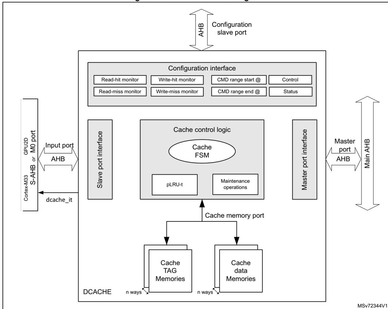
The diagram illustrates the internal architecture of the DCACHE. At the top, an 'AHB Configuration slave port' connects to a 'Configuration interface' block. This block contains several registers: 'Read-hit monitor', 'Write-hit monitor', 'CMD range start @', 'Control', 'Read-miss monitor', 'Write-miss monitor', 'CMD range end @', and 'Status'. Below this, a 'Slave port interface' on the left connects to an 'Input port' for 'GPU2D' and 'Context-M33 S-AHB or M0 port' via an 'AHB' interface, with a 'dcache_it' signal. On the right, a 'Master port interface' connects to a 'Master port' for 'Main AHB' via an 'AHB' interface. The central 'Cache control logic' block contains a 'Cache FSM', 'pLRU-t', and 'Maintenance operations'. At the bottom, a 'Cache memory port' connects to two parallel memory blocks: 'Cache TAG Memories' and 'Cache data Memories', both labeled with 'n ways'. The entire system is labeled 'DCACHE' at the bottom left and 'MSV72344V1' at the bottom right.
9.4.2 DCACHE reset and clocks
The DCACHE is clocked on the Cortex®-M33 S-AHB bus clock.
When the DCACHE reset signal is released, a cache invalidate procedure is automatically launched, making the DCACHE busy (DCACHE_SR = 0x0000 0001).
When this procedure is finished:
- • The DCACHE is invalidated: cold cache, with all cache line valid, dirty, and privilege bits = 0 (DCACHE must be filled up)
- • DCACHE_SR = 0x0000 0002 (reflecting the cache is no longer busy)
- • The DCACHE is disabled: the EN bit in DCACHE_CR holds its reset state (= 0).
Note: When disabled, the DCACHE is bypassed: slave input requests are just forwarded to the master port.
9.4.3 DCACHE TAG memory
The DCACHE TAG memory contains:
- • address tags that indicate which data are contained in the cache data memories
- • validity bits
- • dirty bits
- • privilege bits
There is one valid bit, one dirty bit, and one privilege bit per cache line (per way).
The valid bit enables/disables access to the data cache line: if the line is not valid, the data access (read or write) is performed in the main memory.
The valid bit is set when the cache line is written (refilled by either a read miss or a write-back miss).
Valid bits are reset in any of the below cases:
- • after the DCACHE reset is released
- • when the cache is disabled, by setting EN = 0 in DCACHE_CR (by software)
- • when executing one of the DCACHE invalidate commands, setting by software CACHEINV = 0, or CACHECMD = 0b010 or 0b011 in DCACHE_CR (see Section 9.4.8 ).
The dirty bit indicates that the cache line has up-to-date values with respect to the main memory content (the cache has last right value, the main memory is not up to date).
The dirty bit is set when the cache line is written by a slave port write transaction (only in case of an access with write-back attribute).
Dirty bits are reset in any of the below cases:
- • after the DCACHE reset is released
- • when a line refill is performed on a read miss (on a write-back miss, the refilled cache line is modified by the written data, and dirty bit = 1)
- • when the cache invalidation is performed
- • when executing one of the DCACHE clean operations (cache line written back to the main memory), setting by software CACHECMD = 0b001 or 0b011 in DCACHE_CR (see Section 9.4.8 ).
The privilege bit indicates if the data is managed by a privileged entity. It is assigned according to the value of AHB privileged attribute at the input slave port, for the first access to this line (it is written only during the line refill, on read miss or write-back miss).
The privilege bit holds the same polarity as the privileged attribute: 1 for privileged access, 0 for unprivileged access.
Privilege bits are reset when the cache is invalidated, and after the DCACHE reset is released.
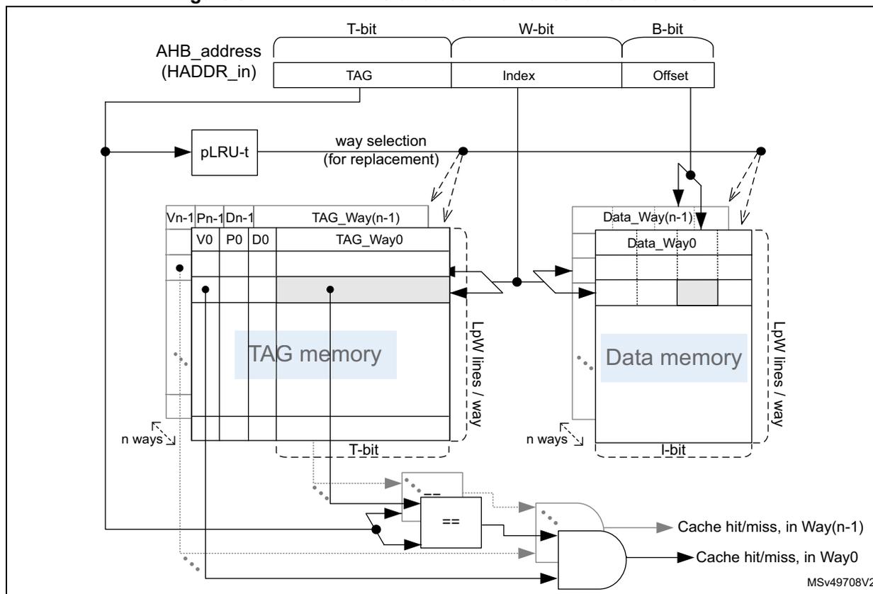
When a cacheable transaction is received at input slave port, its AHB address (HADDR_in) is split into the following fields (see the table below for B and W values):
- • HADDR_in[B-1:0]: address byte offset, indicates which byte to select within a cache line.
- • HADDR_in[B+W-1:B]: address way index, indicates which cache line to select inside each way.
- • HADDR_in[31:B+W]: tag address, to be compared to TAG memory address to check if the requested data is already available (meaning valid) within the DCACHE
Table 91 gives DCACHE main parameters for TAG memory dimensioning.
Figure 31 shows the functional view of TAG and data memories, for an n-way set associative DCACHE.
Table 91. TAG memory dimensioning parameters
| Parameter | Value | Example |
|---|---|---|
| Cache size | \( S \text{ Kbytes} = s \text{ bytes } (s = 1024 \times S) \) | 4 Kbytes = 4096 bytes |
| Cache number of ways | \( n \) | 2 |
| Cache line size | \( L\text{-byte} = l\text{-bit } (l = 8 \times L) \) | 16-byte = 128-bit |
| Number of cache lines (per way) | \( LpW = s / (n \times L) \text{ lines/way} \) | 128 lines/way |
| Address byte offset size | \( B = \log_2(L) \text{ bit} \) | 4-bit |
| Address way index size | \( W = \log_2(LpW) \text{ bit} \) | 7-bit |
| TAG address size | \( T = (32 - W - B) \text{ bit} \) | 21-bit |
Figure 31. DCACHE TAG and data memories functional view
9.4.4 DCACHE enable
To activate the DCACHE functioning, the EN bit must be set in DCACHE_CR control register.
When DCACHE is disabled, it is bypassed and all transactions are copied from slave port to master port in the same clock cycle, and no comparison is performed with TAG address.
DCACHE is by default disabled at boot.
9.4.5 Cacheable and noncacheable traffic
DCACHE is developed for a Cortex ® -M33 core or another bus master peripheral and caches the memory regions addressed by the AHB bus connected to it.
In addition, the AHB bus traffic to the memory regions can be cacheable or noncacheable. An incoming memory request to DCACHE is defined as cacheable according to its AHB transaction memory lookup attribute.
In case of write transaction, the DCACHE write policy is defined as write-through or write-back according to its AHB transaction memory bufferable attribute (see Table 92 ).
These AHB attributes depend on the memory protection unit (MPU) programming for the addressed region.
Table 92. DCACHE cacheability for AHB transaction
| AHB lookup attribute | AHB bufferable attribute | Cacheability |
|---|---|---|
| 0 | x | Read and write: non cacheable |
| 1 | 0 | Read: cacheable Write: (cacheable) write-through |
| 1 | 1 | Read: cacheable Write: (cacheable) write-back |
In case of noncacheable access, the DCACHE is bypassed, meaning that the AHB transaction is propagated unchanged to the master output port.
The bypass does not increase the latency of the access to the targeted memory.
In case of cacheable access, the DCACHE behaves as explained in Section 9.4.6 .
Cacheable memory regions are defined and programmed by the user in the MPU, responsible for the generation of the AHB attribute signals for any transaction addressing a given region.
9.4.6 Cacheable accesses
When the DCACHE receives a cacheable transaction from Cortex ® -M33 or from another bus master peripheral on its slave port, the DCACHE checks if the address requested is present in its TAG memory and if the corresponding cache line is valid.
For read transaction, there are three alternatives:
- • The address is present inside the TAG memory, the cache line is valid: cache read hit , the data is read from cache and provided to the processor in the same cycle.
- • The address is not present in the TAG memory: cache read miss , the data is read from the main memory and provided to the processor, and a cache line refill is performed.
The critical-word-first refill policy insures minimum wait cycles for the processor, since read data can be provided while cache is still performing cache line refill (associated latency is the latency of fetching one word from main memory).
The kind of burst generated on the DCACHE master bus depends on HBURST bit in DCACHE_CR: either INCRw or WRAPw (w being the cache line width, in words).
The AHB transaction attributes are also propagated from the slave input (missing) request to the master output refill request.
- • The address is not present in the TAG memory but belongs to the refill burst from main memory that is currently ongoing: cache read hit as well (hit-under-miss feature).
Whatever the line refill is due to a read or write (missing) transaction, the DCACHE can provide the requested read data as soon as the data is available at its master interface, thus avoiding a miss (with data fetch from main memory).
For write-back transaction (write transaction, with write-back bufferable attribute), there are three alternatives as well:
- • The address is present inside the TAG memory, cache line is valid: cache write-back hit , the data is written in cache.
- • The address is not present in the TAG memory (or the cache line is not valid): cache write-back miss .
First, a line allocation is performed by reading the entire cache line data from main memory. The kind of burst generated on the DCACHE master bus for this line refill depends on HBURST bit in DCACHE_CR: either INCRw or WRAPw (w being the cache line width, in words), and the AHB transaction attributes are propagated from the slave port initial request.
Once the refilled line is written in the DCACHE, the initial data provided on the slave port is written in this DCACHE line (it overwrites the data part of the cache line that was refilled just before).
- • The address is not present in the TAG memory but belongs to the refill burst from main memory that is currently ongoing: cache write-back hit as well (hit-under-miss feature).
Whatever the line refill is due to a read or write (missing) transaction, the DCACHE can write incoming data directly inside the refilled line, thus avoiding a miss (with refill from main memory).
For write-through transaction (write transaction, with write-through bufferable attribute), only two alternatives exist:
- • The address is present inside the TAG memory, cache line is valid: cache write-through hit , the data is written both in cache and in main memory (through master port).
- • The address is not present in the TAG memory (or the cache line is not valid): cache write-through miss , the data incoming at slave port is written only in main memory (unlike the write-back miss, there is no line allocation and data written in cache).
In case of cache refill (due to cache miss), the DCACHE selects which cache line is written with the refill data: as a 2-way set associative cache, one line among two can be used (line pointed by the address index, in each of the two ways). The way selection is based on a pLRU-t replacement algorithm that points, for each index, on the way candidate for the next refill.
If the cache line where the refill data must be written is already valid, the targeted cache line must be evicted first:
- • If the dirty tag of this line equals 0 (clean data), the line is simply invalidated.
- • If it equals 1 (dirty data), the line must be written back in the main memory.
The DCACHE generates a burst write transaction on its master port, with burst type set to INCRw (w being the cache line width, in words), and with AHB memory transaction attribute signals set as below:
- – data (not instruction)
- – privileged = TAG privilege bit
- – write-back (even if it does not care)
- – normal memory
- – cacheable
- – allocate (even if it does not care)
- – nonshareable
These AHB attributes cannot be propagated from the slave port (as it is the case for all other transactions emitted by the DCACHE) because the evicting transaction has no relation with the initial missing transaction. Setting of the AHB attributes is fixed, except for the privileged bit that is copied from the TAG privilege bit of the evicted line.
9.4.7 DCACHE security
The DCACHE implements an Armv8-M TrustZone.
DCACHE configuration registers are protected at system level.
9.4.8 DCACHE maintenance
The DCACHE features several maintenance operations that the software can program in DCACHE_CR control register:
- • Full invalidate: invalidates the whole cache, non interruptible task.
The software can invalidate the whole DCACHE content by programming CACHEINV in DCACHE_CR.
When CACHEINV = 1, the DCACHE control logic sets BUSYF flag in DCACHE_SR status register, and performs the operation of cache invalidation, resetting each TAG valid bit to 0 (one valid bit per cache line). Each dirty and privilege bits are also reset to 0 during cache invalidation to prevent unknown values at next cache line validation. CACHEINV is automatically cleared.
Once the full invalidate operation is finished, the DCACHE automatically clears BUSYF flag, and sets BSYENDF in DCACHE_SR.
If enabled on this flag condition (BSYENDIE = 1 in DCACHE_IER), the DCACHE interrupt is raised. Then, the (empty) cache is available again.
This full invalidate operation is not interruptible, meaning that the cache does not treat any cacheable request while BUSYF = 1. However, non-cacheable traffic is treated (since the request address is not compared to TAG ones), the DCACHE being bypassed in the same clock cycle (same behavior as when the DCACHE is disabled).
- • Invalidation range: invalidates a certain range of addresses in the cache, background task (interruptible).
The software can invalidate a given data region in the DCACHE by programming STARTCMD = 1 and CACHECMD = 0b010 in DCACHE_CR, after the address range was programmed into DCACHE_CMDRSADDRR (range start address) and DCACHE_CMDREADRR (range end address).
The DCACHE control logic then parses the whole TAG memory. If the read line address (TAG address + line index) falls in the programmed address range ( \( DCACHE\_CMDRSADDRR \leq Line\ Addr \leq DCACHE\_CMDREADRR \) ), the
corresponding cache line is invalidated (line TAG bits cleared, valid bit = dirty bit = privilege bit = 0).
When STARTCMD is set, the DCACHE control logic sets BUSYCMDF in DCACHE_SR and launches the invalidate range operation. STARTCMD is also automatically cleared.
Once the operation is finished (all TAG memory parsed), the DCACHE automatically clears BUSYCMDF and sets CMDENDF in DCACHE_SR.
If enabled on this flag condition (CMDENDIE = 1 in DCACHE_IER), the DCACHE interrupt is raised.
During this invalidate range operation, the DCACHE is interruptible, meaning it can accept new incoming requests that take higher priority than the invalidation process. The TAG memory is accessed for invalidate range operation only if not already accessed by an external cache request. This implies that invalidate range execution is usually not performed in one go, but can be interrupted.
- • Clean range: cleans a certain range of addresses in the cache, background task (interruptible).
Cleaning a cache line means making sure that the main memory content is up-to-date with the data, which may have been modified in the cache. The clean operation consists in performing the write-back in the main memory of the cache lines that are tagged as “dirty” (the ones with TAG dirty bit set).
The software can clean a given data region in DCACHE by programming STARTCMD = 1, and CACHECMD = 0b001 in DCACHE_CR, after the address range was programmed into DCACHE_CMDRSADDRR (range start address) and DCACHE_CMDREADRR (range end address).
The DCACHE control logic then parses the whole TAG memory. If the read line address (TAG address + line index) falls in the programmed address range ( \( DCACHE\_CMDRSADDRR \leq Line\ Addr \leq DCACHE\_CMDREADRR \) ), and the corresponding line is dirty, this line is cleaned, meaning the whole cache line is written-back in the memory through the DCACHE master port, and its TAG dirty bit is cleared.
When STARTCMD is set, the DCACHE control logic sets BUSYCMDF in DCACHE_SR and launches the clean range operation. STARTCMD is also automatically cleared.
Once the operation is finished (all TAG memory parsed), the DCACHE automatically clears BUSYCMDF and sets CMDENDF in DCACHE_SR.
If enabled on this flag condition (CMDENDIE = 1 in DCACHE_IER), the DCACHE interrupt is raised.
During this clean range operation, the DCACHE is interruptible, meaning it can accept new incoming requests that take higher priority than the cleaning process. The TAG memory is accessed for clean range operation only if not already accessed by an external cache request. This implies that clean range execution is usually not performed in one go, but can be interrupted.
It is under the software responsibility that no bus initiator attempts to change the content of the region being cleaned until clean range is completed. For that, the software can take advantage of BUSYCMDF flag in DCACHE_SR, and can poll this flag to prevent any spurious access to the area being cleaned.
Alternatively it can also rely on the command end flag (CMDENDF) or on the DCACHE interrupt to detect the end of the clean range execution.
- • Clean and invalidate range: cleans and invalidates a certain range of addresses in the cache, background task (interruptible).
This operation cleans the “dirty” cache lines that belong to the operation address range (the same as the clean range operation), and also invalidates all the (valid) cache lines that belong to this address range (whether they are dirty or not).
The software can launch this clean and invalidate range operation, by programming STARTCMD = 1, and CACHECMD = 0b011 in DCACHE_CR, after the address range was programmed into DCACHE_CMDRSADDRR (range start address) and DCACHE_CMDREADRR (range end address).
This sets and clears the same flags, and potentially the same interrupt as invalidate range or clean range operations.
9.4.9 DCACHE performance monitoring
The DCACHE provides the following monitors for performance analysis:
- • The two 32-bit read-hit and write-hit monitors count the AHB transactions at the DCACHE input (slave port) that do not generate a transaction on the DCACHE output (master port).
These monitors also take into account all accesses whose address is present in the TAG memory, or in the refill buffer (due to a previous miss, and whose data is coming, or is soon to come, from the cache master port) (see Section 9.4.6 ).
- • The two 16-bit read-miss and write-miss monitors count the AHB transactions at the DCACHE input (slave port) that generate a transaction on the DCACHE output (master port).
These monitors also take into account all accesses whose address is not present neither in the TAG memory, nor in the refill buffer.
Upon reaching their maximum values, the monitors do not wrap over.
The software can perform the following tasks:
- • Enable/stop the read (write) hit monitor, through R(W)HITMEN in DCACHE_CR.
- • Reset the read (write) hit monitor, by setting R(W)HITMRST in DCACHE_CR.
- • Enable/stop the read (write) miss monitor, through R(W)MISSMEN in DCACHE_CR.
- • Reset the read (write) miss monitor, by setting R(W)MISSMRST in DCACHE_CR.
To reduce power consumption, these monitors are disabled (stopped) by default.
9.4.10 DCACHE boot
The DCACHE is disabled (EN = 0 in DCACHE_CR) at boot.
Once the boot is finished, the DCACHE can be enabled (software setting EN = 1 in DCACHE_CR).
9.5 DCACHE low-power modes
At product level, the DCACHE reduces the power consumption by loading/storing data from/to the internal DCACHE most of the time, rather than from the bigger and then more power consuming main memories. This reduction is even much higher, since the cached main memories are external.
9.6 DCACHE error management and interrupts
A transaction initiated on the DCACHE master port may return an error (a write attempt into a read-only memory, for instance). If the master port request was propagated from a slave port request, the error is propagated back to the slave port. If ever the master port request is initiated by the DCACHE itself (a cache line is written back into the main memory because of an eviction or a clean operation), the DCACHE receives this functional error and flags it internally by setting the ERRF flag in DCACHE_SR.
In such a case, an interrupt is generated if the corresponding interrupt enable bit is set (ERRIE = 1 in DCACHE_IER).
Another case of potential interrupt generation is at the end of a full invalidate operation: when the cache busy state is finished, the DCACHE sets BSYENDF flag in DCACHE_SR.
An interrupt is then generated if the corresponding interrupt enable bit is set (BSYENDIE = 1 in DCACHE_IER).
Last case is at the end of invalidate and/or clean range operations: when the command busy state is finished, the DCACHE sets CMDENDF flag in DCACHE_SR.
An interrupt is also generated if the corresponding interrupt enable bit is set (CMDENDIE = 1 in DCACHE_IER).
All DCACHE interrupt sources raise the same and unique interrupt signal, dcache_it, and then use the same interrupt vector.
Table 93. DCACHE interrupts
| Interrupt vector | Interrupt event | Event flag | Enable control bit | Interrupt clear method |
|---|---|---|---|---|
| DCACHE | Functional error | ERRF in DCACHE_SR | ERRIE in DCACHE_IER | Set CERRF to 1 in DCACHE_FCR |
| End of busy state (full invalidate finished) | BSYENDF in DCACHE_SR | BSYENDIE in DCACHE_IER | Set CBSYENDF to 1 in DCACHE_FCR | |
| End of cache operations (address range based) | CMDENDF in DCACHE_SR | CMDENDIE in DCACHE_IER | Set CCMENDF to 1 in DCACHE_FCR |
The DCACHE also propagates all AHB bus errors (such as security issues, address decoding issues) from master port back to the S-AHB slave port.
9.7 DCACHE registers
9.7.1 DCACHE control register (DCACHE_CR)
Address offset: 0x000
Reset value: 0x0000 0000
| 31 | 30 | 29 | 28 | 27 | 26 | 25 | 24 | 23 | 22 | 21 | 20 | 19 | 18 | 17 | 16 |
|---|---|---|---|---|---|---|---|---|---|---|---|---|---|---|---|
| HBURST | Res. | Res. | Res. | Res. | Res. | Res. | Res. | WMISSMRST | WHITMRST | WMISSMEN | WHITMEN | RMISSMRST | RHITMRST | RMISSMEN | RHITMEN |
| rw | rw | rw | rw | rw | rw | rw | rw | rw | |||||||
| 15 | 14 | 13 | 12 | 11 | 10 | 9 | 8 | 7 | 6 | 5 | 4 | 3 | 2 | 1 | 0 |
| Res. | Res. | Res. | Res. | START CMD | CACHECMD[2:0] | Res. | Res. | Res. | Res. | Res. | Res. | CACHE INV | EN | ||
| w | rw | rw | rw | w | rw | ||||||||||
Bit 31 HBURST : output burst type for cache master port read accesses
Can be set by software, only when EN = 0.
Master port write accesses are always done in INCR burst type.
0: WRAP
1: INCR
Bits 30:24 Reserved, must be kept at reset value.
Bit 23 WMISSMRST : write-miss monitor reset
0: release the cache miss monitor reset (needed to enable the counting)
1: reset cache write-miss monitor
Bit 22 WHITMRST : write-hit monitor reset
0: release the cache miss monitor reset (needed to enable the counting)
1: reset cache write-hit monitor
Bit 21 WMISSMEN : write-miss monitor enable
0: cache write-miss monitor switched off. Stopping the monitor does not reset it.
1: cache write-miss monitor enabled
Bit 20 WHITMEN : write-hit monitor enable
0: cache write-hit monitor switched off. Stopping the monitor does not reset it.
1: cache write-hit monitor enabled
Bit 19 RMISSMRST : read-miss monitor reset
0: release the cache miss monitor reset (needed to enable the counting)
1: reset cache read-miss monitor
Bit 18 RHITMRST : read-hit monitor reset
0: release the cache miss monitor reset (needed to enable the counting)
1: reset cache read-hit monitor
Bit 17 RMISSMEN : read-miss monitor enable
0: cache read-miss monitor switched off. Stopping the monitor does not reset it.
1: cache read-miss monitor enabled
Bit 16 RHITMEN : read-hit monitor enable
0: cache read-hit monitor switched off. Stopping the monitor does not reset it.
1: cache read-hit monitor enabled
Bits 15:12 Reserved, must be kept at reset value.
Bit 11 STARTCMD : starts maintenance command (maintenance operation defined in CACHECMD).
Can be set by software, only when EN = 1, BUSYCMDF = 0, BUSYF = 0 and CACHECMD = 0b001, 0b010 or 0b011.
Cleared by hardware when the BUSYCMDF flag is set (during cache maintenance operation). Writing 0 has no effect.
0: command operation (cache maintenance) finished
1: start maintenance command (cache maintenance)
Bits 10:8 CACHECMD[2:0] : cache command maintenance operation (cleans and/or invalidates an address range)
Can be set and cleared by software, only when no maintenance command is ongoing (BUSYCMDF = 0).
000: no operation
001: clean range
010: invalidate range
011: clean and invalidate range
others: reserved
Bits 7:2 Reserved, must be kept at reset value.
Bit 1 CACHEINV : full cache invalidation
Can be set by software, only when EN = 1.
Cleared by hardware when the BUSYF flag is set (during full cache invalidation operation).
Writing 0 has no effect.
0: no effect
1: invalidate entire cache (all cache lines valid bit = 0)
Bit 0 EN : enable
0: cache disabled
1: cache enabled
9.7.2 DCACHE status register (DCACHE_SR)
Address offset: 0x004
Reset value: 0x0000 0001
| 31 | 30 | 29 | 28 | 27 | 26 | 25 | 24 | 23 | 22 | 21 | 20 | 19 | 18 | 17 | 16 |
|---|---|---|---|---|---|---|---|---|---|---|---|---|---|---|---|
| Res. | Res. | Res. | Res. | Res. | Res. | Res. | Res. | Res. | Res. | Res. | Res. | Res. | Res. | Res. | Res. |
| 15 | 14 | 13 | 12 | 11 | 10 | 9 | 8 | 7 | 6 | 5 | 4 | 3 | 2 | 1 | 0 |
| Res. | Res. | Res. | Res. | Res. | Res. | Res. | Res. | Res. | Res. | Res. | CMDE NDF | BUSYC MDF | ERRF | BSYEN DF | BUSYF |
| r | r | r | r | r |
Bits 31:5 Reserved, must be kept at reset value.
Bit 4 CMDENDF : command end flag
Cleared by writing DCACHE_FCR.CCMDENDF = 1.
0: cache busy or in idle
1: CACHECMD command finished
Bit 3 BUSYCMDF : command busy flag
0: cache not busy on a CACHECMD command
1: cache busy on a CACHECMD command (clean and/or invalidate an address range)
Bit 2 ERRF : cache error flag
Cleared by writing DCACHE_FCR.GERRF = 1.
0: no error
1: an error occurred during the operation (eviction or clean operation write-back error).
Bit 1 BSYENDF : full invalidate busy end flag
Cleared by writing DCACHE_FCR.GBSYENDF = 1.
0: cache busy or in idle
1: full invalidate CACHEINV operation finished
Bit 0 BUSYF : full invalidate busy flag
0: cache not busy on a CACHEINV operation
1: cache executing a full invalidate CACHEINV operation
9.7.3 DCACHE interrupt enable register (DCACHE_IER)
Address offset: 0x008
Reset value: 0x0000 0000
| 31 | 30 | 29 | 28 | 27 | 26 | 25 | 24 | 23 | 22 | 21 | 20 | 19 | 18 | 17 | 16 |
|---|---|---|---|---|---|---|---|---|---|---|---|---|---|---|---|
| Res. | Res. | Res. | Res. | Res. | Res. | Res. | Res. | Res. | Res. | Res. | Res. | Res. | Res. | Res. | Res. |
| 15 | 14 | 13 | 12 | 11 | 10 | 9 | 8 | 7 | 6 | 5 | 4 | 3 | 2 | 1 | 0 |
| Res. | Res. | Res. | Res. | Res. | Res. | Res. | Res. | Res. | Res. | Res. | CMDE NDIE | Res. | ERRIE | BSYEN DIE | Res. |
| rw | rw | rw |
Bits 31:5 Reserved, must be kept at reset value.
Bit 4 CMDENDIE : interrupt enable on command end
Set by software to enable an interrupt generation at the end of a cache command (clean and/or invalidate an address range)
0: interrupt disabled on command end
1: interrupt enabled on command end
Bit 3 Reserved, must be kept at reset value.
Bit 2 ERRIE : interrupt enable on cache error
Set by software to enable an interrupt generation in case of cache functional error (eviction or clean operation write-back error)
0: interrupt disabled on error
1: interrupt enabled on error
Bit 1 BSYENDIE : interrupt enable on busy end
Set by SW to enable an interrupt generation at the end of a cache full invalidate operation.
0: Interrupt disabled on busy end
1: Interrupt enabled on busy end
Bit 0 Reserved, must be kept at reset value.
9.7.4 DCACHE flag clear register (DCACHE_FCR)
Address offset: 0x00C
Reset value: 0x0000 0000
| 31 | 30 | 29 | 28 | 27 | 26 | 25 | 24 | 23 | 22 | 21 | 20 | 19 | 18 | 17 | 16 |
|---|---|---|---|---|---|---|---|---|---|---|---|---|---|---|---|
| Res. | Res. | Res. | Res. | Res. | Res. | Res. | Res. | Res. | Res. | Res. | Res. | Res. | Res. | Res. | Res. |
| 15 | 14 | 13 | 12 | 11 | 10 | 9 | 8 | 7 | 6 | 5 | 4 | 3 | 2 | 1 | 0 |
| Res. | Res. | Res. | Res. | Res. | Res. | Res. | Res. | Res. | Res. | Res. | CCMD ENDF | Res. | CERRF | CBSYE NDF | Res. |
| w | w | w |
Bits 31:5 Reserved, must be kept at reset value.
Bit 4 CCMDENDF : clear command end flag
Set by software.
0: no effect
1: clears CMDENDF flag in DCACHE_SR
Bit 3 Reserved, must be kept at reset value.
Bit 2 CERRF : clear cache error flag
Set by software.
0: no effect
1: clears ERRF flag in DCACHE_SR
Bit 1 CBSYENDF : clear full invalidate busy end flag
Set by software.
0: no effect
1: clears BSYENDF flag in DCACHE_SR
Bit 0 Reserved, must be kept at reset value.
9.7.5 DCACHE read-hit monitor register (DCACHE_RHMONR)
Address offset: 0x010
Reset value: 0x0000 0000
| 31 | 30 | 29 | 28 | 27 | 26 | 25 | 24 | 23 | 22 | 21 | 20 | 19 | 18 | 17 | 16 |
|---|---|---|---|---|---|---|---|---|---|---|---|---|---|---|---|
| RHITMON[31:16] | |||||||||||||||
| r | r | r | r | r | r | r | r | r | r | r | r | r | r | r | r |
| 15 | 14 | 13 | 12 | 11 | 10 | 9 | 8 | 7 | 6 | 5 | 4 | 3 | 2 | 1 | 0 |
| RHITMON[15:0] | |||||||||||||||
| r | r | r | r | r | r | r | r | r | r | r | r | r | r | r | r |
Bits 31:0 RHITMON[31:0] : cache read-hit monitor counter
9.7.6 DCACHE read-miss monitor register (DCACHE_RMMONR)
Address offset: 0x014
Reset value: 0x0000 0000
| 31 | 30 | 29 | 28 | 27 | 26 | 25 | 24 | 23 | 22 | 21 | 20 | 19 | 18 | 17 | 16 |
| Res. | Res. | Res. | Res. | Res. | Res. | Res. | Res. | Res. | Res. | Res. | Res. | Res. | Res. | Res. | Res. |
| 15 | 14 | 13 | 12 | 11 | 10 | 9 | 8 | 7 | 6 | 5 | 4 | 3 | 2 | 1 | 0 |
| RMISSMON[15:0] | |||||||||||||||
| r | r | r | r | r | r | r | r | r | r | r | r | r | r | r | r |
Bits 31:16 Reserved, must be kept at reset value.
Bits 15:0 RMISSMON[15:0] : cache read-miss monitor counter
9.7.7 DCACHE write-hit monitor register (DCACHE_WHMONR)
Address offset: 0x020
Reset value: 0x0000 0000
| 31 | 30 | 29 | 28 | 27 | 26 | 25 | 24 | 23 | 22 | 21 | 20 | 19 | 18 | 17 | 16 |
| WHITMON[31:16] | |||||||||||||||
| r | r | r | r | r | r | r | r | r | r | r | r | r | r | r | r |
| 15 | 14 | 13 | 12 | 11 | 10 | 9 | 8 | 7 | 6 | 5 | 4 | 3 | 2 | 1 | 0 |
| WHITMON[15:0] | |||||||||||||||
| r | r | r | r | r | r | r | r | r | r | r | r | r | r | r | r |
Bits 31:0 WHITMON[31:0] : cache write-hit monitor counter
9.7.8 DCACHE write-miss monitor register (DCACHE_WMMONR)
Address offset: 0x024
Reset value: 0x0000 0000
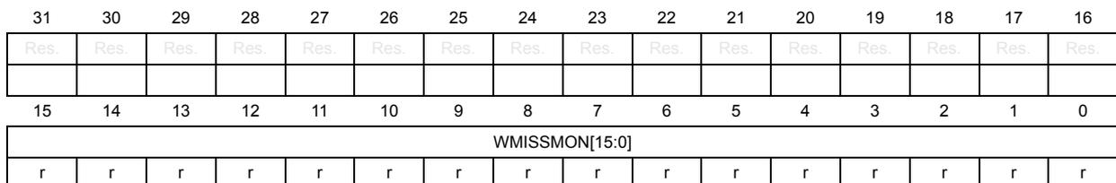
| 31 | 30 | 29 | 28 | 27 | 26 | 25 | 24 | 23 | 22 | 21 | 20 | 19 | 18 | 17 | 16 |
| Res. | Res. | Res. | Res. | Res. | Res. | Res. | Res. | Res. | Res. | Res. | Res. | Res. | Res. | Res. | Res. |
| 15 | 14 | 13 | 12 | 11 | 10 | 9 | 8 | 7 | 6 | 5 | 4 | 3 | 2 | 1 | 0 |
| WMISSMON[15:0] | |||||||||||||||
| r | r | r | r | r | r | r | r | r | r | r | r | r | r | r | r |
Bits 31:16 Reserved, must be kept at reset value.
Bits 15:0 WMISSMON[15:0] : cache write-miss monitor counter
9.7.9 DCACHE command range start address register (DCACHE_CMDRSADDRR)
Address offset: 0x028
Reset value: 0x0000 0000
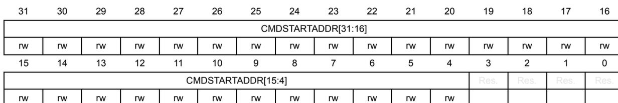
| 31 | 30 | 29 | 28 | 27 | 26 | 25 | 24 | 23 | 22 | 21 | 20 | 19 | 18 | 17 | 16 |
| CMDSTARTADDR[31:16] | |||||||||||||||
| rw | rw | rw | rw | rw | rw | rw | rw | rw | rw | rw | rw | rw | rw | rw | rw |
| 15 | 14 | 13 | 12 | 11 | 10 | 9 | 8 | 7 | 6 | 5 | 4 | 3 | 2 | 1 | 0 |
| CMDSTARTADDR[15:4] | Res. | Res. | Res. | Res. | |||||||||||
| rw | rw | rw | rw | rw | rw | rw | rw | rw | rw | rw | rw | ||||
Bits 31:4 CMDSTARTADDR[31:4] : start address of range to which the cache maintenance command specified in DCACHE_CR.CACHECMD field applies
This register must be set before DCACHE_CR.CACHECMD is written.
Note: bit 4 is reserved on the STM32U59x/5Ax/5Fx/5Gx.
Bits 3:0 Reserved, must be kept at reset value.
9.7.10 DCACHE command range end address register (DCACHE_CMDREADRR)
Address offset: 0x02C
Reset value: 0x0000 0000
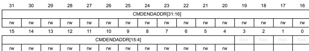
| 31 | 30 | 29 | 28 | 27 | 26 | 25 | 24 | 23 | 22 | 21 | 20 | 19 | 18 | 17 | 16 |
| CMDENDADDR[31:16] | |||||||||||||||
| rw | rw | rw | rw | rw | rw | rw | rw | rw | rw | rw | rw | rw | rw | rw | rw |
| 15 | 14 | 13 | 12 | 11 | 10 | 9 | 8 | 7 | 6 | 5 | 4 | 3 | 2 | 1 | 0 |
| CMDENDADDR[15:4] | Res. | Res. | Res. | Res. | |||||||||||
| rw | rw | rw | rw | rw | rw | rw | rw | rw | rw | rw | rw | ||||
Bits 31:4 CMDENDADDR[31:4] : end address of range to which the cache maintenance command specified in DCACHE_CR.CACHECMD field applies
This register must be set before DCACHE_CR.CACHECMD is written.
Note: bit 4 is reserved on the STM32U59x/5Ax/5Fx/5Gx
Bits 3:0 Reserved, must be kept at reset value.
9.7.11 DCACHE register map
Table 94. DCACHE register map and reset values
| Offset | Register name | 31 | 30 | 29 | 28 | 27 | 26 | 25 | 24 | 23 | 22 | 21 | 20 | 19 | 18 | 17 | 16 | 15 | 14 | 13 | 12 | 11 | 10 | 9 | 8 | 7 | 6 | 5 | 4 | 3 | 2 | 1 | 0 |
|---|---|---|---|---|---|---|---|---|---|---|---|---|---|---|---|---|---|---|---|---|---|---|---|---|---|---|---|---|---|---|---|---|---|
| 0x000 | DCACHE_CR | HBURST | Res. | Res. | Res. | Res. | Res. | Res. | Res. | WMISSMRST | WHITMRST | WMISSMEN | WHITMEN | RMISSMRST | RHITMRST | RMISSMEN | RHITMEN | Res. | Res. | Res. | Res. | STARTCMD | CACHECMD [2:0] | Res. | Res. | Res. | Res. | Res. | Res. | CACHEINV | EN | ||
| Reset value | 0 | 0 | 0 | 0 | 0 | 0 | 0 | 0 | 0 | 0 | 0 | 0 | 0 | 0 | 0 |
Table 94. DCACHE register map and reset values (continued)
| Offset | Register name | 31 | 30 | 29 | 28 | 27 | 26 | 25 | 24 | 23 | 22 | 21 | 20 | 19 | 18 | 17 | 16 | 15 | 14 | 13 | 12 | 11 | 10 | 9 | 8 | 7 | 6 | 5 | 4 | 3 | 2 | 1 | 0 | |
|---|---|---|---|---|---|---|---|---|---|---|---|---|---|---|---|---|---|---|---|---|---|---|---|---|---|---|---|---|---|---|---|---|---|---|
| 0x004 | DCACHE_SR | Res. | Res. | Res. | Res. | Res. | Res. | Res. | Res. | Res. | Res. | Res. | Res. | Res. | Res. | Res. | Res. | Res. | Res. | Res. | Res. | Res. | Res. | Res. | Res. | Res. | Res. | Res. | Res. | Res. | CMDENDF | BUSYCMDF | ERRF | BSYENDF |
| Reset value | 0 | 0 | 0 | 1 | ||||||||||||||||||||||||||||||
| 0x008 | DCACHE_IER | Res. | Res. | Res. | Res. | Res. | Res. | Res. | Res. | Res. | Res. | Res. | Res. | Res. | Res. | Res. | Res. | Res. | Res. | Res. | Res. | Res. | Res. | Res. | Res. | Res. | Res. | Res. | Res. | Res. | CMDENDIE | ERRIE | BSYENDIE | Res. |
| Reset value | 0 | 0 | 0 | |||||||||||||||||||||||||||||||
| 0x00C | DCACHE_FCR | Res. | Res. | Res. | Res. | Res. | Res. | Res. | Res. | Res. | Res. | Res. | Res. | Res. | Res. | Res. | Res. | Res. | Res. | Res. | Res. | Res. | Res. | Res. | Res. | Res. | Res. | Res. | Res. | Res. | CMDENDF | CERRF | BSYENDF | Res. |
| Reset value | 0 | 0 | 0 | |||||||||||||||||||||||||||||||
| 0x010 | DCACHE_RHMONR | RHITMON[31:0] | ||||||||||||||||||||||||||||||||
| Reset value | 0 | 0 | 0 | 0 | 0 | 0 | 0 | 0 | 0 | 0 | 0 | 0 | 0 | 0 | 0 | 0 | 0 | 0 | 0 | 0 | 0 | 0 | 0 | 0 | 0 | 0 | 0 | 0 | 0 | 0 | 0 | 0 | ||
| 0x014 | DCACHE_RMMONR | Res. | Res. | Res. | Res. | Res. | Res. | Res. | Res. | Res. | Res. | Res. | Res. | Res. | Res. | Res. | Res. | RMISSMON[15:0] | ||||||||||||||||
| Reset value | 0 | 0 | 0 | 0 | 0 | 0 | 0 | 0 | 0 | 0 | 0 | 0 | 0 | 0 | 0 | |||||||||||||||||||
| 0x020 | DCACHE_WHMONR | WHITMON[31:0] | ||||||||||||||||||||||||||||||||
| Reset value | 0 | 0 | 0 | 0 | 0 | 0 | 0 | 0 | 0 | 0 | 0 | 0 | 0 | 0 | 0 | 0 | 0 | 0 | 0 | 0 | 0 | 0 | 0 | 0 | 0 | 0 | 0 | 0 | 0 | 0 | 0 | 0 | ||
| 0x024 | DCACHE_WMMONR | Res. | Res. | Res. | Res. | Res. | Res. | Res. | Res. | Res. | Res. | Res. | Res. | Res. | Res. | Res. | Res. | WMISSMON[15:0] | ||||||||||||||||
| Reset value | 0 | 0 | 0 | 0 | 0 | 0 | 0 | 0 | 0 | 0 | 0 | 0 | 0 | 0 | 0 | |||||||||||||||||||
| 0x028 | DCACHE_CMDRSADDRR | CMDSTARTADDR[31:4] | Res. | Res. | Res. | |||||||||||||||||||||||||||||
| Reset value | 0 | 0 | 0 | 0 | 0 | 0 | 0 | 0 | 0 | 0 | 0 | 0 | 0 | 0 | 0 | 0 | 0 | 0 | 0 | 0 | 0 | 0 | 0 | 0 | 0 | 0 | 0 | 0 | 0 | |||||
| 0x02C | DCACHE_CMDREADRR | CMDENDADDR[31:4] | Res. | Res. | Res. | |||||||||||||||||||||||||||||
| Reset value | 0 | 0 | 0 | 0 | 0 | 0 | 0 | 0 | 0 | 0 | 0 | 0 | 0 | 0 | 0 | 0 | 0 | 0 | 0 | 0 | 0 | 0 | 0 | 0 | 0 | 0 | 0 | 0 | 0 | |||||
Refer to Section 2.3: Memory organization for the register boundary addresses.