6. RAM configuration controller (RAMCFG)
6.1 RAMCFG introduction
The RAMCFG configures the features of the internal SRAMs (SRAM1/2/3/4/5/6 and BKPSRAM).
6.2 RAMCFG main features
The internal SRAM supports some of the features listed hereafter, configured in RAMCFG:
- • Error code correction (ECC):
- – Single error detection and correction with interrupt generation
- – Double error detection with interrupt or NMI generation
- – Status with failing address
- • Write protection (1-Kbyte granularity)
- • Programmable wait states for voltage scaling range 4
- • SRAM software erase
6.3 RAMCFG functional description
6.3.1 Internal SRAMs features
Up to seven SRAMs are embedded in the devices, each with specific features:
- • SRAM1/2/3/5/6 are the main SRAMs. The SRAM4 is in the SRAM used for peripheral low-power background autonomous mode (LPBAM) in Stop 2 mode.
Table 45. SRAM structure
| SRAM | STM32U535/545 | STM32U575/585 | STM32U59x/5Ax | STM32U5Fx/5Gx |
|---|---|---|---|---|
| SRAM1 | 192 Kbytes (3 blocks of 64 Kbytes) | 768 Kbytes (12 blocks of 64 Kbytes) | ||
| SRAM2 | 64 Kbytes (8-Kbyte and 56-Kbyte blocks, can be retained in Standby mode) | |||
| SRAM3 | N/A | 512 Kbytes (8 blocks of 64 Kbytes) | 832 Kbytes (13 blocks of 64 Kbytes) | |
| SRAM4 | 16 Kbytes | |||
| SRAM5 | N/A | N/A | 832 Kbytes (13 blocks of 64 Kbytes) | |
| SRAM6 | N/A | N/A | N/A | 512 Kbytes (8 blocks of 64 Kbytes) |
| BKPSRAM | 2 Kbytes | |||
The backup SRAM (BKPSRAM) can be retained in all low-power modes and when \( V_{DD} \) is off in \( V_{BAT} \) mode (see Section 10: Power control (PWR) for more details).
- All internal SRAMs are erased by hardware in case of readout protection (RDP) level regression to level 0.5 or level 0. Refer to Section 7: Embedded flash memory (FLASH) for more details.
- The SRAM2 is erased when a system reset occurs if the SRAM2_RST option bit is selected in the flash memory user option bytes. SRAM1/3/4/5/6 are erased when a system reset occurs if the SRAM_RST option bit is selected in the flash memory user option bytes. Refer to Section 7: Embedded flash memory (FLASH) for more details.
- The SRAM2 and optionally the BKPSRAM are protected by the tamper detection circuit, and are erased by hardware in case of tamper detection. BKPSRAM is also erased by hardware in case of a backup domain reset. Refer to Section 64: Tamper and backup registers (TAMP) for more details.
- The RAMCFG embeds the registers related to the internal SRAMs ECC, write protection, wait-state configuration, and software erase.
The table below summarizes the features supported by each internal SRAM.
Table 46. Internal SRAMs features
| SRAM feature | SRAM1 | SRAM2 | SRAM3 | SRAM4 | SRAM5 | SRAM6 | BKPSRAM |
|---|---|---|---|---|---|---|---|
| DMA accessibility in Stop 0/1 modes | X | X | X | X | X | X | X |
| DMA accessibility in Stop 2 mode | - | - | - | X | - | - | - |
| Optional retention in Standby mode | - | X | - | - | - | - | X |
| Optional retention in V BAT mode | - | - | - | - | - | - | X |
| Erased with RDP regression | X | X | X | X | X | X | X |
| Erased or blocked by tamper detection | - | X | - | - | - | - | X (1) |
| Optionally erased with system reset | X | X | X | X | X | X | - |
| Software erase | X | X | X | X | X | X | X |
| ECC | - | X | X | - | - | - | X |
| Write protection | - | X | - | - | - | - | - |
| Wait states | X | X | X | X | X | X | X |
1. Optional: BKPSRAM can be configured to be erased or not on tamper detection.
6.3.2 Error code correction (SRAM2, SRAM3, BKPSRAM)
The ECC is supported by SRAM2/3 and BKPSRAM when enabled with the SRAM2_ECC, SRAM3_ECC, and BKPRAM_ECC user option bits. Refer to Section 7: Embedded flash memory (FLASH) for more details.
Seven ECC bits are added per 32 bits of SRAM, allowing two bits error detection, and one bit error correction on memory read access.
As the ECC is calculated and checked for a 32-bit word, the byte and half-word write accesses are managed by the SRAM interface by first reading the whole word, then write the word again with the new byte/half-word value. ECC double errors are also detected during these byte or half-word AHB write accesses (read/modify/write done by interface). The byte or half-word write access latency is WSC[2:0] + 2 AHB clock cycles (see Section 6.3.4 ).
Caution: In case of a byte or half-word write on SRAM with ECC, the read/modify/write operation is done in a buffer. The buffer content is written into the SRAM two AHB clock cycles after the SRAM AHB is released (when SRAM is no more accessed).
Single and double ECC errors
When a single error is detected, it is automatically corrected, and SEDC/CSEDC bits are set in RAMCFG_MxISR and RAMCFG_MxICR respectively. The associated ECC single error address RAMCFG_MxSEAR is updated only if the single error interrupt is enabled (SEIE bit of RAMCFG_MxIER is set), and if the ALE bit is set in RAMCFG_MxCR.
Caution: Single errors cannot be detected when the SEDC bit is set.
When a double error is detected, DED and CDED bits are set in RAMCFG_MxISR and RAMCFG_MxICR respectively. The associated ECC double error address RAMCFG_MxDEAR is updated only if the double error interrupt is enabled (DEIE bit of RAMCFG_MxIER is set) or NMI is enabled by ECCNMI, and if the ALE bit is set in RAMCFG_MxCR.
Caution: Double errors cannot be detected when the DED bit is set.
SRAM3 ECC specific management
When the ECC is enabled for SRAM3, only the first 256 Kbytes of SRAM3 are with ECC. The next 192 Kbytes for STM32U575/585 or 512 Kbytes for STM32U59x/5Ax/5Fx/5Gx are without ECC, and the last block is used to store the ECC, so cannot be used for application.
The figure below shows the SRAM areas, when SRAM2 and SRAM3 ECC are enabled.
Figure 22. SRAM1, SRAM2 with ECC and SRAM3 with ECC memory map
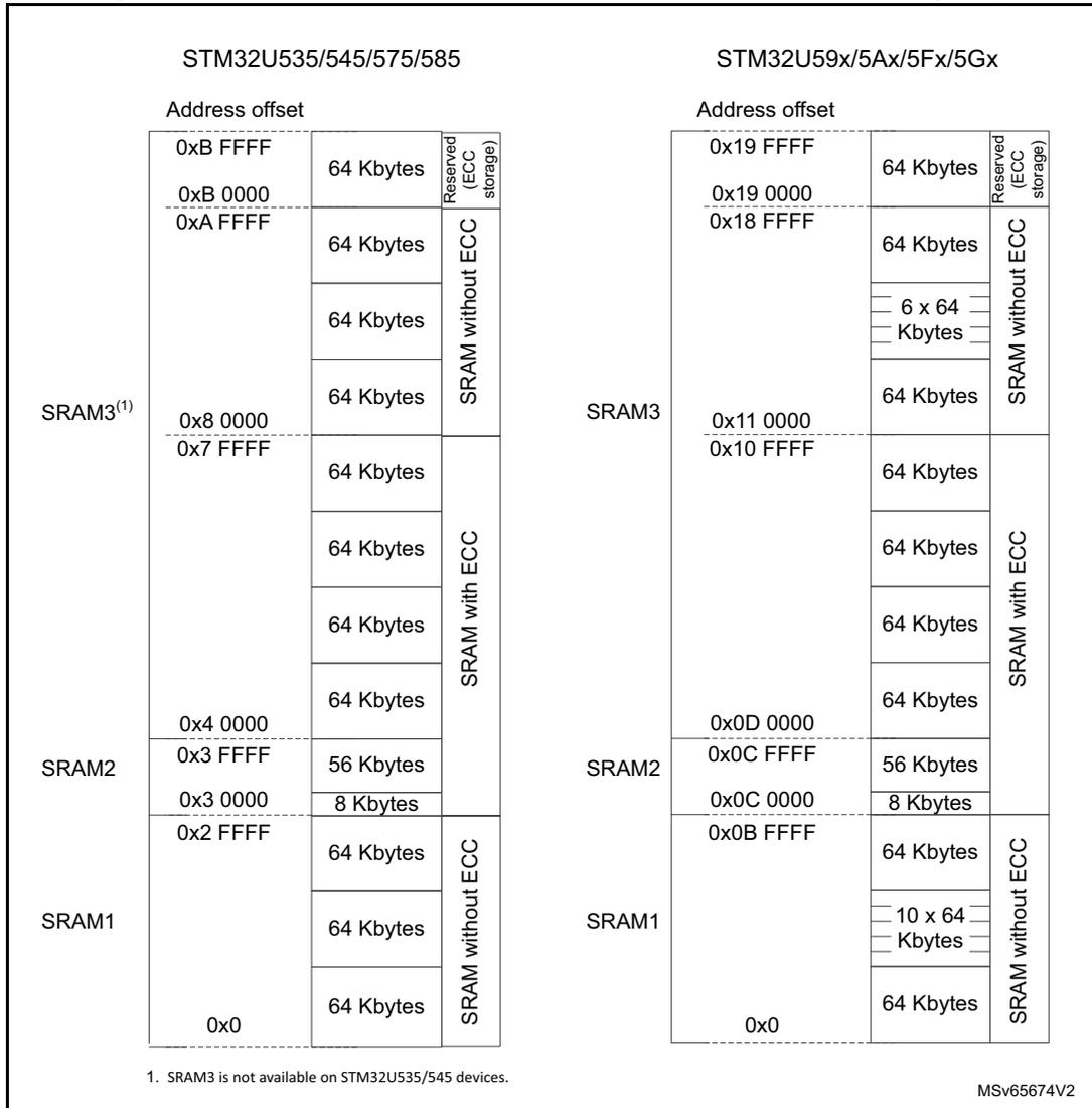
The figure displays two memory maps for different STM32 microcontroller families. Both maps show SRAM1, SRAM2, and SRAM3 areas with their respective address offsets and sizes. The left map is for STM32U535/545/575/585, and the right map is for STM32U59x/5Ax/5Fx/5Gx. The maps detail the allocation of SRAM3 into 'Reserved (ECC storage)' and 'SRAM without ECC' or 'SRAM with ECC' sections. SRAM2 and SRAM1 are also shown with their sizes and ECC status.
| STM32U535/545/575/585 | STM32U59x/5Ax/5Fx/5Gx | ||||||
|---|---|---|---|---|---|---|---|
| Address offset | Address offset | ||||||
| SRAM3 (1) | 0xB FFFF | 64 Kbytes | Reserved (ECC storage) | SRAM3 | 0x19 FFFF | 64 Kbytes | Reserved (ECC storage) |
| 0xB 0000 | 0x19 0000 | ||||||
| 0xA FFFF | 64 Kbytes | SRAM without ECC | 0x18 FFFF | 64 Kbytes | SRAM without ECC | ||
| 64 Kbytes | 6 x 64 Kbytes | ||||||
| 64 Kbytes | 64 Kbytes | ||||||
| 64 Kbytes | 64 Kbytes | ||||||
| 0x8 0000 | 64 Kbytes | SRAM with ECC | 0x11 0000 | 64 Kbytes | SRAM with ECC | ||
| 64 Kbytes | 64 Kbytes | ||||||
| 64 Kbytes | 64 Kbytes | ||||||
| 64 Kbytes | 64 Kbytes | ||||||
| 0x4 0000 | 0x0D 0000 | ||||||
| 0x3 FFFF | 56 Kbytes | SRAM2 | 0x0C FFFF | 56 Kbytes | SRAM2 | ||
| 0x3 0000 | 8 Kbytes | 0x0C 0000 | 8 Kbytes | ||||
| SRAM1 | 0x2 FFFF | 64 Kbytes | SRAM without ECC | 0x0B FFFF | 64 Kbytes | SRAM without ECC | |
| 64 Kbytes | 10 x 64 Kbytes | ||||||
| 64 Kbytes | 64 Kbytes | ||||||
| 0x0 | 0x0 | ||||||
1. SRAM3 is not available on STM32U535/545 devices.
MSv65674V2
When ECC is enabled by user option bits, the ECCE bit is automatically set after system reset in the related RAMCFG_MxCR.
The ECC can be deactivated by executing the following software sequence:
- 1. Write 0xAE in RAMCFG_MxECCKEYR.
- 2. Write 0x75 in RAMCFG_MxECCKEYR.
- 3. Write 0 in the ECCE bit of RAMCFG_MxCR.
In case ECC is deactivated (ECCE = 0), the SRAM3 ECC storage area (from offset 0xB0000 to offset 0xBFFFF) can be read and written as other SRAM3 areas. In order to test the ECC mechanism, only the first 256 Kbytes of SRAM3 can be modified, 1 or 2 bits by word (for single or double error test respectively).
The procedure to check ECC is the following:
- 1. On an erased memory, write data with ECC on.
- 2. Disable ECC.
- 3. Write same data with 1- or 2-bit modification (for single or double error test respectively).
- 4. Enable ECC.
- 5. Wait until ECCE bit of RAMCFG_M3CR is read at 1.
- 6. Read data. Enabled interrupt is generated because of single or double error.
Steps 4 and 5 instructions must not be located in SRAM3 with ECC area. Any access to SRAM3 with ECC area by the other masters is forbidden during the steps 4 and 5 executions, until they are completed.
Warning: The ECC fault injection test triggers a system break event in TIM1/8/15/16/17, if the SPL bit is set in SYSCFG_CFGR2. This implies that the test must be performed while the PWM outputs of the timers are in idle state.
6.3.3 Write protection (SRAM2)
The SRAM2 is made of 64 1-Kbyte pages. Each 1-Kbyte page can be write-protected by setting its corresponding PxWP (x = 0 to 63) bit in RAMCFG_M2WPR1 and RAMCFG_M2WPR2.
6.3.4 Read access latency
To correctly read data from SRAMs, the number of wait states must be correctly programmed in WSC[2:0] field of RAMCFG_MxCR, depending on AHB clock frequency (HCLK) and voltage scaling range, as shown in the table below.
Table 47. Number of wait states versus HCLK frequency and voltage range scaling
| Wait states (WS) (latency) | HCLK (MHz) | |||
|---|---|---|---|---|
| V CORE range 1 | V CORE range 2 | V CORE range 3 | V CORE range 4 and Stop 0/1/2 modes (1) | |
| 0 WS (1 AHB cycle) | ≤ 160 | ≤ 110 | ≤ 55 | ≤ 16 |
| 1 WS (2 AHB cycle) | - | - | - | ≤ 25 |
1. The system clock can be requested in Stop 0/1/2 modes to perform DMA transfers to SRAM.
6.3.5 Software erase
SRAM erase can be requested by executing this software sequence:
- 1. Write 0xCA in RAMCFG_MxERKEYR.
- 2. Write 0x53 in RAMCFG_MxERKEYR.
- 3. Write 1 in RAMCFG_MxCR.
SRAMBUSY flag is set in the related SRAM interrupt status register as long as the erase is on going.
The total duration of each SRAM erase is N AHB clock cycles, where N is the size of the SRAM in 32-bit words.
If the SRAM is read or written while an erase is on going, wait states are inserted on the AHB bus until the end of the erase operation.
6.4 RAMCFG low-power modes
Table 48. Effect of low-power modes on RAMCFG
| Mode | Description |
|---|---|
| Sleep | No effect. RAMCFG interrupts cause the device to exit the Sleep mode. |
| Stop | The content of RAMCFG registers is kept. The ECC is functional and ECC error interrupt or NMI causes the device to exit from Stop 0 and Stop 1 modes. |
| Standby | The RAMCFG peripheral is powered down and must be reinitialized after exiting Standby mode. |
6.5 RAMCFG interrupts
The table below gives the list of RAMCFG interrupt requests.
Table 49. RAMCFG interrupt requests
| Interrupt acronym | Interrupt event | Event flag | Enable control bit | Interrupt clear method | Exit Sleep mode | Exit Stop mode | Exit Standby mode |
|---|---|---|---|---|---|---|---|
| RAMCFG | ECC single error detection and correction | SEDC | SEIE | Write 1 in CSEDC | Yes | Yes (1) | No |
| ECC double error detection | DED | DEIE = 1 and ECCNMI = 0 | Write 1 in CDED | Yes | Yes (1) | No | |
| NMI | ECC double error detection | DED | ECCNMI | Write 1 in CDED | Yes | Yes (1) | No |
1. Stop 0 and Stop 1 modes only.
6.6 RAMCFG registers
In the registers described below, x refers to:
- • SRAM1/2/3/4 when x = 1/2/3/4 respectively
- • BKPSRAM when x = 5
- • SRAM5 when x = 6
- • SRAM6 when x = 7
6.6.1 RAMCFG memory x control register (RAMCFG_MxCR)
Address offset: 0x040 * (x - 1), (x = 1 to 7)
Reset value: 0x0000 000X
ECCE reset value depends on ECC enable user option bit.
| 31 | 30 | 29 | 28 | 27 | 26 | 25 | 24 | 23 | 22 | 21 | 20 | 19 | 18 | 17 | 16 |
|---|---|---|---|---|---|---|---|---|---|---|---|---|---|---|---|
| Res. | Res. | Res. | Res. | Res. | Res. | Res. | Res. | Res. | Res. | Res. | Res. | Res. | WSC[2:0] | ||
| rw | rw | rw | |||||||||||||
| 15 | 14 | 13 | 12 | 11 | 10 | 9 | 8 | 7 | 6 | 5 | 4 | 3 | 2 | 1 | 0 |
| Res. | Res. | Res. | Res. | Res. | Res. | Res. | SRAM ER | Res. | Res. | Res. | ALE | Res. | Res. | Res. | ECCE |
| rs | rw | rw | |||||||||||||
Bits 31:19 Reserved, must be kept at reset value.
Bits 18:16 WSC[2:0] : Wait state configuration
This field is used to program the number of wait states inserted on the AHB when reading the SRAM, depending on its access time.
000: 0 wait state
001: 1 wait state
...
111: 7 wait states (not needed)
Bits 15:9 Reserved, must be kept at reset value.
Bit 8 SRAMER : SRAM erase
This bit can be set by software only after writing the unlock sequence in the ERASEKEY field of the RAMCFG_MxERKEYR register. Setting this bit starts the SRAM erase. This bit is automatically cleared by hardware at the end of the erase operation.
0: No erase operation on going
1: Erase operation on going
Bits 7:5 Reserved, must be kept at reset value.
Bit 4 ALE : Address latch enable
0: Failing address not stored in the SRAMx ECC single/double error address registers
1: Failing address stored in the SRAMx ECC single/double error address registers
Note: This bit is reserved and must be kept at reset value in SRAM1/4/5/6 control registers.
Bits 3:1 Reserved, must be kept at reset value.
Bit 0 ECCE : ECC enable.
This bit reset value is defined by the user option bit configuration. When set, it can be cleared by software only after writing the unlock sequence in the RAMCFG_MxECCKEYR register.
0: ECC disabled
1: ECC enabled
Note: This bit is reserved and must be kept at reset value in SRAM1/4/5/6 control registers.
6.6.2 RAMCFG memory x interrupt enable register (RAMCFG_MxIER)
Address offset: 0x004 + 0x40 * (x - 1), (x = 2, 3, 5)
Reset value: 0x0000 0000
| 31 | 30 | 29 | 28 | 27 | 26 | 25 | 24 | 23 | 22 | 21 | 20 | 19 | 18 | 17 | 16 |
|---|---|---|---|---|---|---|---|---|---|---|---|---|---|---|---|
| Res. | Res. | Res. | Res. | Res. | Res. | Res. | Res. | Res. | Res. | Res. | Res. | Res. | Res. | Res. | Res. |
| 15 | 14 | 13 | 12 | 11 | 10 | 9 | 8 | 7 | 6 | 5 | 4 | 3 | 2 | 1 | 0 |
| Res. | Res. | Res. | Res. | Res. | Res. | Res. | Res. | Res. | Res. | Res. | Res. | ECCNMI | Res. | DEIE | SEIE |
| rs | rw | rw |
Bits 31:4 Reserved, must be kept at reset value.
Bit 3 ECCNMI : Double error NMI
This bit is set by software and cleared only by a global RAMCFG reset.
0: NMI not generated in case of ECC double error
1: NMI generated in case of ECC double error
Note: if ECCNMI is set, the RAMCFG maskable interrupt is not generated whatever DEIE bit value.
Bit 2 Reserved, must be kept at reset value.
Bit 1 DEIE : ECC double error interrupt enable
0: Double error interrupt disabled
1: Double error interrupt enabled
Bit 0 SEIE : ECC single error interrupt enable
0: Single error interrupt disabled
1: Single error interrupt enabled
6.6.3 RAMCFG memory interrupt status register (RAMCFG_MxISR)
Address offset: 0x008 + 0x40 * (x - 1), (x = 1 to 7)
Reset value: 0x0000 0000
| 31 | 30 | 29 | 28 | 27 | 26 | 25 | 24 | 23 | 22 | 21 | 20 | 19 | 18 | 17 | 16 |
|---|---|---|---|---|---|---|---|---|---|---|---|---|---|---|---|
| Res. | Res. | Res. | Res. | Res. | Res. | Res. | Res. | Res. | Res. | Res. | Res. | Res. | Res. | Res. | Res. |
| 15 | 14 | 13 | 12 | 11 | 10 | 9 | 8 | 7 | 6 | 5 | 4 | 3 | 2 | 1 | 0 |
| Res. | Res. | Res. | Res. | Res. | Res. | Res. | SRAM BUSY | Res. | Res. | Res. | Res. | Res. | Res. | DED | SEDC |
| r | r | r |
Bits 31:9 Reserved, must be kept at reset value.
Bit 8 SRAMBUSY : SRAM busy with erase operation
0: No erase operation on going
1: Erase operation on going
Note: Depending on the SRAM, the erase operation can be performed due to software request, system reset if the option bit is enabled, tamper detection or readout protection regression (see Table 46).
Bits 7:2 Reserved, must be kept at reset value.
Bit 1 DED : ECC double error detected
0: No double error
1: Double error detected
Note: This bit is reserved and must be kept at reset value in SRAM1/4/5/6 interrupt status registers.
Bit 0 SEDC : ECC single error detected and corrected
0: No single error
1: Single error detected and corrected
Note: This bit is reserved and must be kept at reset value in SRAM1/4/5/6 interrupt status registers.
6.6.4 RAMCFG memory x ECC single error address register (RAMCFG_MxSEAR)
Address offset: \( 0x00C + 0x40 * (x - 1) \) , ( \( x = 2, 3, 5 \) )
Reset value: 0x0000 0000
| 31 | 30 | 29 | 28 | 27 | 26 | 25 | 24 | 23 | 22 | 21 | 20 | 19 | 18 | 17 | 16 |
|---|---|---|---|---|---|---|---|---|---|---|---|---|---|---|---|
| ESEA[31:16] | |||||||||||||||
| r | r | r | r | r | r | r | r | r | r | r | r | r | r | r | r |
| 15 | 14 | 13 | 12 | 11 | 10 | 9 | 8 | 7 | 6 | 5 | 4 | 3 | 2 | 1 | 0 |
| ESEA[15:0] | |||||||||||||||
| r | r | r | r | r | r | r | r | r | r | r | r | r | r | r | r |
Bits 31:0 ESEA[31:0] : ECC single error address
When the ALE bit is set in the RAMCFG_MxCR register, this field is updated with the address corresponding to the ECC single error.
6.6.5 RAMCFG memory x ECC double error address register (RAMCFG_MxDEAR)
Address offset: \( 0x010 + 0x40 * (x - 1) \) , ( \( x = 2, 3, 5 \) )
Reset value: 0x0000 0000
| 31 | 30 | 29 | 28 | 27 | 26 | 25 | 24 | 23 | 22 | 21 | 20 | 19 | 18 | 17 | 16 |
|---|---|---|---|---|---|---|---|---|---|---|---|---|---|---|---|
| EDEA[31:16] | |||||||||||||||
| r | r | r | r | r | r | r | r | r | r | r | r | r | r | r | r |
| 15 | 14 | 13 | 12 | 11 | 10 | 9 | 8 | 7 | 6 | 5 | 4 | 3 | 2 | 1 | 0 |
| EDEA[15:0] | |||||||||||||||
| r | r | r | r | r | r | r | r | r | r | r | r | r | r | r | r |
Bits 31:0 EDEA[31:0] : ECC double error address
When the ALE bit is set in the RAMCFG_MxCR register, this field is updated with the address corresponding to the ECC double error.
6.6.6 RAMCFG memory x interrupt clear register x (RAMCFG_MxICR)
Address offset: \( 0x014 + 0x40 * (x - 1) \) , ( \( x = 2, 3, 5 \) )
Reset value: 0x0000 0000
| 31 | 30 | 29 | 28 | 27 | 26 | 25 | 24 | 23 | 22 | 21 | 20 | 19 | 18 | 17 | 16 |
|---|---|---|---|---|---|---|---|---|---|---|---|---|---|---|---|
| Res. | Res. | Res. | Res. | Res. | Res. | Res. | Res. | Res. | Res. | Res. | Res. | Res. | Res. | Res. | Res. |
| 15 | 14 | 13 | 12 | 11 | 10 | 9 | 8 | 7 | 6 | 5 | 4 | 3 | 2 | 1 | 0 |
| Res. | Res. | Res. | Res. | Res. | Res. | Res. | Res. | Res. | Res. | Res. | Res. | Res. | Res. | CDED | CSEDC |
| rw | rw |
Bits 31:2 Reserved, must be kept at reset value.
Bit 1 CDED : Clear ECC double error detected
Writing 1 to this flag clears the DED bit in the RAMCFG_MxISR register. Reading this flag returns the DED value.
Bit 0 CSEDC : Clear ECC single error detected and corrected
Writing 1 to this flag clears the SEDC bit in the RAMCFG_MxISR register. Reading this flag returns the SEDC value.
6.6.7 RAMCFG memory 2 write protection register 1 (RAMCFG_M2WPR1)
Address offset: 0x058
Reset value: 0x0000 0000
| 31 | 30 | 29 | 28 | 27 | 26 | 25 | 24 | 23 | 22 | 21 | 20 | 19 | 18 | 17 | 16 |
|---|---|---|---|---|---|---|---|---|---|---|---|---|---|---|---|
| P31WP | P30WP | P29WP | P28WP | P27WP | P26WP | P25WP | P24WP | P23WP | P22WP | P21WP | P20WP | P19WP | P18WP | P17WP | P16WP |
| rs | rs | rs | rs | rs | rs | rs | rs | rs | rs | rs | rs | rs | rs | rs | rs |
| 15 | 14 | 13 | 12 | 11 | 10 | 9 | 8 | 7 | 6 | 5 | 4 | 3 | 2 | 1 | 0 |
| P15WP | P14WP | P13WP | P12WP | P11WP | P10WP | P9WP | P8WP | P7WP | P6WP | P5WP | P4WP | P3WP | P2WP | P1WP | P0WP |
| rs | rs | rs | rs | rs | rs | rs | rs | rs | rs | rs | rs | rs | rs | rs | rs |
Bits 31:0 PyWP : SRAM2 1-Kbyte page y write protection (y = 31 to 0)
These bits are set by software and cleared only by a global RAMCFG reset.
0: Write protection of SRAM2 1-Kbyte page y is disabled.
1: Write protection of SRAM2 1-Kbyte page y is enabled.
6.6.8 RAMCFG memory 2 write protection register 2 (RAMCFG_M2WPR2)
Address offset: 0x05C
Reset value: 0x0000 0000
| 31 | 30 | 29 | 28 | 27 | 26 | 25 | 24 | 23 | 22 | 21 | 20 | 19 | 18 | 17 | 16 |
|---|---|---|---|---|---|---|---|---|---|---|---|---|---|---|---|
| P63WP | P62WP | P61WP | P60WP | P59WP | P58WP | P57WP | P56WP | P55WP | P54WP | P53WP | P52WP | P51WP | P50WP | P49WP | P48WP |
| rs | rs | rs | rs | rs | rs | rs | rs | rs | rs | rs | rs | rs | rs | rs | rs |
| 15 | 14 | 13 | 12 | 11 | 10 | 9 | 8 | 7 | 6 | 5 | 4 | 3 | 2 | 1 | 0 |
| P47WP | P46WP | P45WP | P44WP | P43WP | P42WP | P41WP | P40WP | P39WP | P38WP | P37WP | P36WP | P35WP | P34WP | P33WP | P32WP |
| rs | rs | rs | rs | rs | rs | rs | rs | rs | rs | rs | rs | rs | rs | rs | rs |
Bits 31:0 PyWP : SRAM2 1-Kbyte page y write protection (y = 63 to 32)
These bits are set by software and cleared only by a global RAMCFG reset.
0: Write protection of SRAM2 1-Kbyte page y is disabled.
1: Write protection of SRAM2 1-Kbyte page y is enabled.
6.6.9 RAMCFG memory x ECC key register (RAMCFG_MxECCKEYR)
Address offset: 0x024 + 0x40 * (x - 1), (x = 2, 3, 5)
Reset value: 0x0000 0000
| 31 | 30 | 29 | 28 | 27 | 26 | 25 | 24 | 23 | 22 | 21 | 20 | 19 | 18 | 17 | 16 |
|---|---|---|---|---|---|---|---|---|---|---|---|---|---|---|---|
| Res. | Res. | Res. | Res. | Res. | Res. | Res. | Res. | Res. | Res. | Res. | Res. | Res. | Res. | Res. | Res. |
| 15 | 14 | 13 | 12 | 11 | 10 | 9 | 8 | 7 | 6 | 5 | 4 | 3 | 2 | 1 | 0 |
| Res. | Res. | Res. | Res. | Res. | Res. | Res. | Res. | ECCKEY[7:0] | |||||||
| w | w | w | w | w | w | w | w | ||||||||
Bits 31:8 Reserved, must be kept at reset value.
Bits 7:0 ECCKEY[7:0] : ECC write protection key
The following steps are required to unlock the write protection of ECCE in RAMCFG_MxCR.
1) Write 0xAE into ECCKEY[7:0].
2) Write 0x75 into ECCKEY[7:0].
Note: Writing a wrong key reactivates the write protection.
6.6.10 RAMCFG memory x erase key register (RAMCFG_MxERKEYR)
Address offset: 0x028 + 0x40 * (x - 1), (x = 1 to 7)
Reset value: 0x0000 0000
| 31 | 30 | 29 | 28 | 27 | 26 | 25 | 24 | 23 | 22 | 21 | 20 | 19 | 18 | 17 | 16 |
|---|---|---|---|---|---|---|---|---|---|---|---|---|---|---|---|
| Res. | Res. | Res. | Res. | Res. | Res. | Res. | Res. | Res. | Res. | Res. | Res. | Res. | Res. | Res. | Res. |
| 15 | 14 | 13 | 12 | 11 | 10 | 9 | 8 | 7 | 6 | 5 | 4 | 3 | 2 | 1 | 0 |
| Res. | Res. | Res. | Res. | Res. | Res. | Res. | Res. | ||||||||
| w | w | w | w | w | w | w | w |
Bits 31:8 Reserved, must be kept at reset value.
Bits 7:0 ERASEKEY[7:0] : Erase write protection key
The following steps are required to unlock the write protection of SRAMER in RAMCFG_MxCR.
1) Write 0xCA into ERASEKEY[7:0].
2) Write 0x53 into ERASEKEY[7:0].
Note: Writing a wrong key reactivates the write protection.
6.6.11 RAMCFG register map
Table 50. RAMCFG register map and reset values
| Offset | Register name | 31 | 30 | 29 | 28 | 27 | 26 | 25 | 24 | 23 | 22 | 21 | 20 | 19 | 18 | 17 | 16 | 15 | 14 | 13 | 12 | 11 | 10 | 9 | 8 | 7 | 6 | 5 | 4 | 3 | 2 | 1 | 0 |
|---|---|---|---|---|---|---|---|---|---|---|---|---|---|---|---|---|---|---|---|---|---|---|---|---|---|---|---|---|---|---|---|---|---|
| 0x00 | RAMCFG_M1CR | Res. | Res. | Res. | Res. | Res. | Res. | Res. | Res. | Res. | Res. | Res. | Res. | Res. | WSC[2:0] | Res. | Res. | Res. | Res. | Res. | Res. | Res. | Res. | Res. | SRAMER | Res. | Res. | Res. | Res. | Res. | Res. | Res. | Res. |
| Reset value | 0 0 0 | 0 | |||||||||||||||||||||||||||||||
| 0x04 | Reserved | Reserved | |||||||||||||||||||||||||||||||
| 0x08 | RAMCFG_M1ISR | Res. | Res. | Res. | Res. | Res. | Res. | Res. | Res. | Res. | Res. | Res. | Res. | Res. | Res. | Res. | Res. | Res. | Res. | Res. | Res. | Res. | Res. | Res. | SRAMBUSY | Res. | Res. | Res. | Res. | Res. | Res. | Res. | |
| Reset value | 0 | ||||||||||||||||||||||||||||||||
| 0x0C to 0x24 | Reserved | Reserved | |||||||||||||||||||||||||||||||
| 0x28 | RAMCFG_M1ERKEYR | Res. | Res. | Res. | Res. | Res. | Res. | Res. | Res. | Res. | Res. | Res. | Res. | Res. | Res. | Res. | Res. | Res. | Res. | Res. | Res. | Res. | Res. | Res. | Res. | ERASEKEY[7:0] | |||||||
| Reset value | 0 | 0 | 0 | 0 | 0 | 0 | 0 | ||||||||||||||||||||||||||
| 0x2C to 0x3C | Reserved | Reserved | |||||||||||||||||||||||||||||||
Table 50. RAMCFG register map and reset values (continued)
| Offset | Register name | 31 | 30 | 29 | 28 | 27 | 26 | 25 | 24 | 23 | 22 | 21 | 20 | 19 | 18 | 17 | 16 | 15 | 14 | 13 | 12 | 11 | 10 | 9 | 8 | 7 | 6 | 5 | 4 | 3 | 2 | 1 | 0 |
|---|---|---|---|---|---|---|---|---|---|---|---|---|---|---|---|---|---|---|---|---|---|---|---|---|---|---|---|---|---|---|---|---|---|
| 0x40 | RAMCFG_M2CR | Res. | Res. | Res. | Res. | Res. | Res. | Res. | Res. | Res. | Res. | Res. | Res. | Res. | WSC[2:0] | Res. | Res. | Res. | Res. | Res. | Res. | Res. | SRAMER | Res. | Res. | Res. | Res. | ALE | Res. | Res. | ECCE | ||
| Reset value | 0 | 0 | 0 | 0 | 0 | x | |||||||||||||||||||||||||||
| 0x44 | RAMCFG_M2IER | Res. | Res. | Res. | Res. | Res. | Res. | Res. | Res. | Res. | Res. | Res. | Res. | Res. | Res. | Res. | Res. | Res. | Res. | Res. | Res. | Res. | Res. | Res. | Res. | Res. | Res. | Res. | Res. | ECNNMI | Res. | DEIE | SEIE |
| Reset value | 0 | 0 | 0 | ||||||||||||||||||||||||||||||
| 0x48 | RAMCFG_M2ISR | Res. | Res. | Res. | Res. | Res. | Res. | Res. | Res. | Res. | Res. | Res. | Res. | Res. | Res. | Res. | Res. | Res. | Res. | Res. | Res. | Res. | Res. | Res. | SRAMBUSY | Res. | Res. | Res. | Res. | Res. | Res. | DED | SEDC |
| Reset value | 0 | 0 | 0 | ||||||||||||||||||||||||||||||
| 0x4C | RAMCFG_M2SEAR | ESEA[31:0] | |||||||||||||||||||||||||||||||
| Reset value | 0 | 0 | 0 | 0 | 0 | 0 | 0 | 0 | 0 | 0 | 0 | 0 | 0 | 0 | 0 | 0 | 0 | 0 | 0 | 0 | 0 | 0 | 0 | 0 | 0 | 0 | 0 | 0 | 0 | 0 | 0 | 0 | |
| 0x50 | RAMCFG_M2DEAR | EDEA[31:0] | |||||||||||||||||||||||||||||||
| Reset value | 0 | 0 | 0 | 0 | 0 | 0 | 0 | 0 | 0 | 0 | 0 | 0 | 0 | 0 | 0 | 0 | 0 | 0 | 0 | 0 | 0 | 0 | 0 | 0 | 0 | 0 | 0 | 0 | 0 | 0 | 0 | 0 | |
| 0x54 | RAMCFG_M2ICR | Res. | Res. | Res. | Res. | Res. | Res. | Res. | Res. | Res. | Res. | Res. | Res. | Res. | Res. | Res. | Res. | Res. | Res. | Res. | Res. | Res. | Res. | Res. | Res. | Res. | Res. | Res. | Res. | Res. | Res. | CDED | CSEDC |
| Reset value | 0 | 0 | |||||||||||||||||||||||||||||||
| 0x58 | RAMCFG_M2WPR1 | P31WP | P30WP | P29WP | P28WP | P27WP | P26WP | P25WP | P24WP | P23WP | P22WP | P21WP | P20WP | P19WP | P18WP | P17WP | P16WP | P15WP | P14WP | P13WP | P12WP | P11WP | P10WP | P9WP | P8WP | P7WP | P6WP | P5WP | P4WP | P3WP | P2WP | P1WP | P0WP |
| Reset value | 0 | 0 | 0 | 0 | 0 | 0 | 0 | 0 | 0 | 0 | 0 | 0 | 0 | 0 | 0 | 0 | 0 | 0 | 0 | 0 | 0 | 0 | 0 | 0 | 0 | 0 | 0 | 0 | 0 | 0 | 0 | 0 | |
| 0x5C | RAMCFG_M2WPR2 | P63WP | P62WP | P61WP | P60WP | P59WP | P58WP | P57WP | P56WP | P55WP | P54WP | P53WP | P52WP | P51WP | P50WP | P49WP | P48WP | P47WP | P46WP | P45WP | P44WP | P43WP | P42WP | P41WP | P40WP | P39WP | P38WP | P37WP | P36WP | P35WP | P34WP | P33WP | P32WP |
| Reset value | 0 | 0 | 0 | 0 | 0 | 0 | 0 | 0 | 0 | 0 | 0 | 0 | 0 | 0 | 0 | 0 | 0 | 0 | 0 | 0 | 0 | 0 | 0 | 0 | 0 | 0 | 0 | 0 | 0 | 0 | 0 | 0 | |
| 0x60 | Reserved | Reserved | |||||||||||||||||||||||||||||||
| 0x64 | RAMCFG_M2ECCKEYR | Res. | ECCKEY[7:0] | ||||||||||||||||||||||||||||||
| Reset value | 0 | 0 | 0 | 0 | 0 | 0 | 0 | 0 | |||||||||||||||||||||||||
| 0x68 | RAMCFG_M2ERKEYR | Res. | ERASEKEY[7:0] | ||||||||||||||||||||||||||||||
| Reset value | 0 | 0 | 0 | 0 | 0 | 0 | 0 | 0 | |||||||||||||||||||||||||
| 0x6C to 0x7C | Reserved | Reserved | |||||||||||||||||||||||||||||||
| 0x80 | RAMCFG_M3CR | Res. | Res. | Res. | Res. | Res. | Res. | Res. | Res. | Res. | Res. | Res. | Res. | Res. | WSC[2:0] | Res. | Res. | Res. | Res. | Res. | Res. | Res. | SRAMER | Res. | Res. | Res. | Res. | ALE | Res. | Res. | ECCE | ||
| Reset value | 0 | 0 | 0 | 0 | 0 | 0 | |||||||||||||||||||||||||||
| 0x84 | RAMCFG_M3IER | Res. | Res. | Res. | Res. | Res. | Res. | Res. | Res. | Res. | Res. | Res. | Res. | Res. | Res. | Res. | Res. | Res. | Res. | Res. | Res. | Res. | Res. | Res. | Res. | Res. | Res. | Res. | Res. | ECNNMI | Res. | DEIE | SEIE |
| Reset value | 0 | 0 | 0 | ||||||||||||||||||||||||||||||
| 0x88 | RAMCFG_M3ISR | Res. | Res. | Res. | Res. | Res. | Res. | Res. | Res. | Res. | Res. | Res. | Res. | Res. | Res. | Res. | Res. | Res. | Res. | Res. | Res. | Res. | Res. | Res. | SRAMBUSY | Res. | Res. | Res. | Res. | Res. | Res. | DED | SEDC |
| Reset value | 0 | 0 | 0 | ||||||||||||||||||||||||||||||
| 0x8C | RAMCFG_M3SEAR | ESEA[31:0] | |||||||||||||||||||||||||||||||
| Reset value | 0 | 0 | 0 | 0 | 0 | 0 | 0 | 0 | 0 | 0 | 0 | 0 | 0 | 0 | 0 | 0 | 0 | 0 | 0 | 0 | 0 | 0 | 0 | 0 | 0 | 0 | 0 | 0 | 0 | 0 | 0 | 0 | |
| 0x90 | RAMCFG_M3DEAR | EDEA[31:0] | |||||||||||||||||||||||||||||||
| Reset value | 0 | 0 | 0 | 0 | 0 | 0 | 0 | 0 | 0 | 0 | 0 | 0 | 0 | 0 | 0 | 0 | 0 | 0 | 0 | 0 | 0 | 0 | 0 | 0 | 0 | 0 | 0 | 0 | 0 | 0 | 0 | 0 | |
Table 50. RAMCFG register map and reset values (continued)
| Offset | Register name | 31 | 30 | 29 | 28 | 27 | 26 | 25 | 24 | 23 | 22 | 21 | 20 | 19 | 18 | 17 | 16 | 15 | 14 | 13 | 12 | 11 | 10 | 9 | 8 | 7 | 6 | 5 | 4 | 3 | 2 | 1 | 0 |
|---|---|---|---|---|---|---|---|---|---|---|---|---|---|---|---|---|---|---|---|---|---|---|---|---|---|---|---|---|---|---|---|---|---|
| 0x094 | RAMCFG_M3ICR | Res | Res | Res | Res | Res | Res | Res | Res | Res | Res | Res | Res | Res | Res | Res | Res | Res | Res | Res | Res | Res | Res | Res | Res | Res | Res | Res | Res | Res | Res | Res | CDED |
| Reset value | 0 | ||||||||||||||||||||||||||||||||
| 0x098- 0x0A0 | Reserved | Reserved | |||||||||||||||||||||||||||||||
| 0x0A4 | RAMCFG_M3ECCKEYR | Res | Res | Res | Res | Res | Res | Res | Res | Res | Res | Res | Res | Res | Res | Res | Res | Res | Res | Res | Res | Res | Res | Res | Res | ECCKEY[7:0] | |||||||
| Reset value | 0 | 0 | 0 | 0 | 0 | 0 | 0 | ||||||||||||||||||||||||||
| 0x0A8 | RAMCFG_M3ERKEYR | Res | Res | Res | Res | Res | Res | Res | Res | Res | Res | Res | Res | Res | Res | Res | Res | Res | Res | Res | Res | Res | Res | Res | Res | ERASEKEY[7:0] | |||||||
| Reset value | 0 | 0 | 0 | 0 | 0 | 0 | 0 | ||||||||||||||||||||||||||
| 0x0AC- 0x0BC | Reserved | Reserved | |||||||||||||||||||||||||||||||
| 0x0C0 | RAMCFG_M4CR | Res | Res | Res | Res | Res | Res | Res | Res | Res | Res | Res | Res | Res | Res | WSC[2:0] | Res | Res | Res | Res | Res | Res | Res | Res | SRAMER | Res | Res | Res | Res | Res | Res | Res | Res |
| Reset value | 0 | 0 | |||||||||||||||||||||||||||||||
| 0x0C4 | Reserved | Reserved | |||||||||||||||||||||||||||||||
| 0x0C8 | RAMCFG_M4ISR | Res | Res | Res | Res | Res | Res | Res | Res | Res | Res | Res | Res | Res | Res | Res | Res | Res | Res | Res | Res | Res | Res | Res | SRAMBUSY | Res | Res | Res | Res | Res | Res | Res | |
| Reset value | 0 | ||||||||||||||||||||||||||||||||
| 0x0CC to 0x0E4 | Reserved | Reserved | |||||||||||||||||||||||||||||||
| 0x0E8 | RAMCFG_M4ERKEYR | Res | Res | Res | Res | Res | Res | Res | Res | Res | Res | Res | Res | Res | Res | Res | Res | Res | Res | Res | Res | Res | Res | Res | Res | ERASEKEY[2:0] | |||||||
| Reset value | 0 | 0 | 0 | 0 | 0 | 0 | 0 | ||||||||||||||||||||||||||
| 0x0EC- 0x0FC | Reserved | Reserved | |||||||||||||||||||||||||||||||
| 0x100 | RAMCFG_M5CR | Res | Res | Res | Res | Res | Res | Res | Res | Res | Res | Res | Res | Res | Res | WSC[2:0] | Res | Res | Res | Res | Res | Res | Res | Res | SRAMER | Res | Res | Res | ALE | Res | Res | ECCE | |
| Reset value | 0 | 0 | 0 | x | |||||||||||||||||||||||||||||
| 0x104 | RAMCFG_M5IER | Res | Res | Res | Res | Res | Res | Res | Res | Res | Res | Res | Res | Res | Res | Res | Res | Res | Res | Res | Res | Res | Res | Res | Res | Res | Res | Res | ECCNMI | Res | DEIE | SEIE | |
| Reset value | 0 | 0 | 0 | ||||||||||||||||||||||||||||||
| 0x108 | RAMCFG_M5ISR | Res | Res | Res | Res | Res | Res | Res | Res | Res | Res | Res | Res | Res | Res | Res | Res | Res | Res | Res | Res | Res | Res | Res | SRAMBUSY | Res | Res | Res | Res | Res | DED | SEDC | |
| Reset value | 0 | 0 | 0 | ||||||||||||||||||||||||||||||
| 0x10C | RAMCFG_M5SEAR | ESEA[31:0] | |||||||||||||||||||||||||||||||
| Reset value | 0 | 0 | 0 | 0 | 0 | 0 | 0 | 0 | 0 | 0 | 0 | 0 | 0 | 0 | 0 | 0 | 0 | 0 | 0 | 0 | 0 | 0 | 0 | 0 | 0 | 0 | 0 | 0 | 0 | 0 | 0 | ||
| 0x110 | RAMCFG_M5DEAR | EDEA[31:0] | |||||||||||||||||||||||||||||||
| Reset value | 0 | 0 | 0 | 0 | 0 | 0 | 0 | 0 | 0 | 0 | 0 | 0 | 0 | 0 | 0 | 0 | 0 | 0 | 0 | 0 | 0 | 0 | 0 | 0 | 0 | 0 | 0 | 0 | 0 | 0 | 0 | ||
| 0x114 | RAMCFG_M5ICR | Res | Res | Res | Res | Res | Res | Res | Res | Res | Res | Res | Res | Res | Res | Res | Res | Res | Res | Res | Res | Res | Res | Res | Res | Res | Res | Res | Res | Res | Res | CDED | |
| Reset value | 0 | ||||||||||||||||||||||||||||||||
| 0x118- 0x120 | Reserved | Reserved | |||||||||||||||||||||||||||||||
| 0x124 | RAMCFG_M5ECCKEYR | Res | Res | Res | Res | Res | Res | Res | Res | Res | Res | Res | Res | Res | Res | Res | Res | Res | Res | Res | Res | Res | Res | Res | Res | ECCKEY[7:0] | |||||||
| Reset value | 0 | 0 | 0 | 0 | 0 | 0 | 0 | ||||||||||||||||||||||||||
Table 50. RAMCFG register map and reset values (continued)
| Offset | Register name | 31 | 30 | 29 | 28 | 27 | 26 | 25 | 24 | 23 | 22 | 21 | 20 | 19 | 18 | 17 | 16 | 15 | 14 | 13 | 12 | 11 | 10 | 9 | 8 | 7 | 6 | 5 | 4 | 3 | 2 | 1 | 0 |
|---|---|---|---|---|---|---|---|---|---|---|---|---|---|---|---|---|---|---|---|---|---|---|---|---|---|---|---|---|---|---|---|---|---|
| 0x128 | RAMCFG_M5ERKEYR | Res | Res | Res | Res | Res | Res | Res | Res | Res | Res | Res | Res | Res | Res | Res | Res | Res | Res | Res | Res | Res | Res | Res | Res | ERASEKEY[7:0] | |||||||
| Reset value | 0 | 0 | 0 | 0 | 0 | 0 | 0 | 0 | |||||||||||||||||||||||||
| 0x12C to 0x13C | Reserved | Reserved | |||||||||||||||||||||||||||||||
| 0x140 | RAMCFG_M6CR | Res | Res | Res | Res | Res | Res | Res | Res | Res | Res | Res | Res | Res | WSC[2:0] | Res | Res | Res | Res | Res | Res | Res | Res | Res | o SRAMER | Res | Res | Res | Res | Res | Res | Res | Res |
| Reset value | 0 0 0 | 0 | |||||||||||||||||||||||||||||||
| 0x144 | Reserved | Reserved | |||||||||||||||||||||||||||||||
| 0x148 | RAMCFG_M6ISR | Res | Res | Res | Res | Res | Res | Res | Res | Res | Res | Res | Res | Res | Res | Res | Res | Res | Res | Res | Res | Res | Res | Res | o SRAMBUSY | Res | Res | Res | Res | Res | Res | Res | Res |
| Reset value | 0 | ||||||||||||||||||||||||||||||||
| 0x14C to 0x164 | Reserved | Reserved | |||||||||||||||||||||||||||||||
| 0x168 | RAMCFG_M6ERKEYR | Res | Res | Res | Res | Res | Res | Res | Res | Res | Res | Res | Res | Res | Res | Res | Res | Res | Res | Res | Res | Res | Res | Res | Res | ERASEKEY[7:0] | |||||||
| Reset value | 0 | 0 | 0 | 0 | 0 | 0 | 0 | 0 | |||||||||||||||||||||||||
| 0x180 | RAMCFG_M7CR | Res | Res | Res | Res | Res | Res | Res | Res | Res | Res | Res | Res | Res | WSC[2:0] | Res | Res | Res | Res | Res | Res | Res | Res | Res | o SRAMER | Res | Res | Res | Res | Res | Res | Res | Res |
| Reset value | 0 0 0 | 0 | |||||||||||||||||||||||||||||||
| 0x184 | Reserved | Reserved | |||||||||||||||||||||||||||||||
| 0x188 | RAMCFG_M7ISR | Res | Res | Res | Res | Res | Res | Res | Res | Res | Res | Res | Res | Res | Res | Res | Res | Res | Res | Res | Res | Res | Res | Res | o SRAMBUSY | Res | Res | Res | Res | Res | Res | Res | Res |
| Reset value | 0 | ||||||||||||||||||||||||||||||||
| 0x18C to 0x1A4 | Reserved | Reserved | |||||||||||||||||||||||||||||||
| 0x1A8 | RAMCFG_M7ERKEYR | Res | Res | Res | Res | Res | Res | Res | Res | Res | Res | Res | Res | Res | Res | Res | Res | Res | Res | Res | Res | Res | Res | Res | Res | ERASEKEY[7:0] | |||||||
| Reset value | 0 | 0 | 0 | 0 | 0 | 0 | 0 | 0 | |||||||||||||||||||||||||