5. Global TrustZone controller (GTZC)
5.1 GTZC introduction
This section describes the global TrustZone controller (GTZC) block that contains the following subblocks:
- •
TZSC:
TrustZone security controller
This subblock defines the secure/privileged state of slave peripherals. It also controls the sub-region area size and properties for the watermark memory peripheral controller (MPCWM). The TZSC informs some peripherals (such as RCC or GPIOs) about the secure status of each securable peripheral, by sharing with RCC and I/O logic. - •
MPCBB:
memory protection controller - block based
This subblock configures the internal RAM in a TrustZone-system product having segmented SRAM (pages of 512 bytes) with programmable-security and privileged attributes. - •
TZIC:
TrustZone illegal access controller
This subblock gathers all illegal access events in the system and generates a secure interrupt towards NVIC.
These subblocks are used to configure TrustZone system security in a product having bus agents with programmable-security and privileged attributes such as:
- • on-chip RAM with programmable secure and/or privileged blocks (pages)
- • AHB and APB peripherals with programmable security and/or privileged access
- • off-chip memories with secure and/or privileged areas
5.2 GTZC main features
The GTZC main features are listed below:
- • 3 independent 32-bit AHB interface for TZSC, TZIC and MPCBB
- • TZIC accessible only with secure transactions
- • Secure and nonsecure access supported for privileged and unprivileged part of TZSC and MPCBB
- • Set of registers to define product security settings:
- – Secure/privileged blocks for internal SRAMs
- – Secure/privileged regions for external memories and internal backup SRAM
- – Secure/privileged access mode for securable peripherals
- – Secure/privileged access mode for securable masters
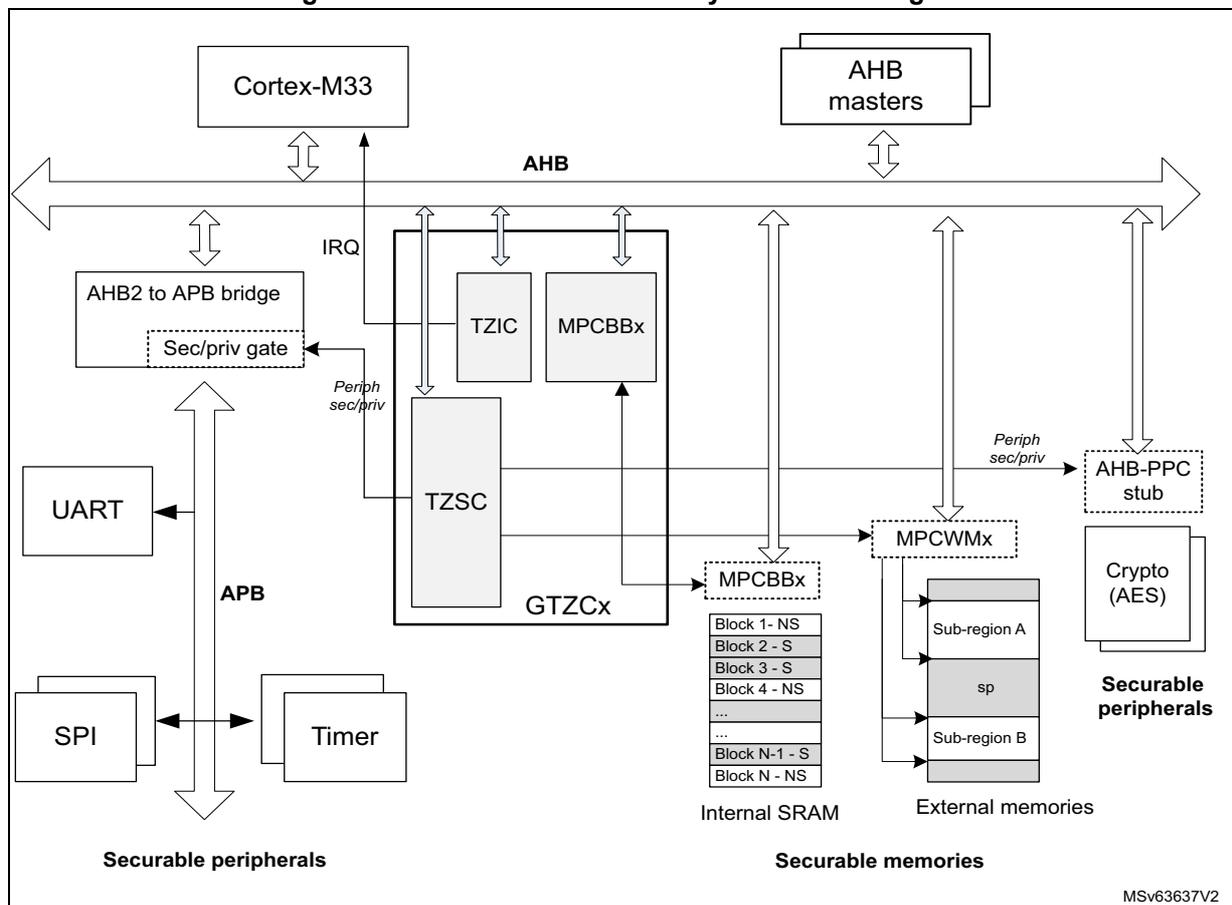
GTZC TrustZone system architecture
The Armv8-M supports security per TrustZone-M model with isolation between:
- • a secure world, where usually security sensitive applications are run and critical resources are located
- • a nonsecure or public world (such as usual nonsecure operating system and user space)
The TrustZone architecture is extended beyond AHB and Armv8-M with:
- • AHB/APB bridge used as secure gate to block or propagate secure/nonsecure and privileged/unprivileged transaction towards APB agents
- • PPC (peripheral protection controller) used as secure gate to block or propagate secure/nonsecure and privileged/unprivileged transaction towards AHB agents
- • TrustZone block-based MPC firewalls used as secure gate to filter secure/nonsecure, privileged/unprivileged access towards internal SRAMs
- • TrustZone watermark MPC firewalls used as secure gate to filter secure/nonsecure, privileged/unprivileged access towards external memories
AHB and APB Peripherals can be categorized as:
- • privileged: peripherals protected by AHB/APB firewall stub that is controlled from TZSC to define privilege properties
- • secure: peripherals always protected by an AHB/APB firewall stub. These peripherals are always secure (such as TZIC)
- • securable: peripherals protected by an AHB/APB firewall stub that is controlled from TZSC to define security properties (optional)
- • nonsecure and unprivileged: peripherals connected directly to AHB/APB interconnect without any secure gate
- • TrustZone-aware: peripherals connected directly to AHB or APB bus and implementing a specific TrustZone behavior (such as a subset of registers being secure). TrustZone-aware AHB masters always drive HNONSEC signal according to their security mode (such as Armv8-M core or DMA)
AHB securable masters can be configured in the TZSC to be secure/nonsecure and/or privileged/unprivileged.
Application information
The TZSC, MPCBB and TZIC can be used in one of the following ways:
- • programmed during secure boot only, locked and not changed afterwards
- • dynamically re-programmed when using specific application code or secure kernel (microvisor). When not locked, MPC secure blocks or region size can be changed by secure software executing from the secure FLASH region or secure SRAM. Same remark applies to the GTZC_TZSC_SECCFGRx/PRIVCFGRx registers that define secure/privileged state of each peripheral.
The Armv8-M security architecture with secure, securable and TrustZone-aware peripherals is shown in the figure below.
Figure 18. GTZC in Armv8-M subsystem block diagram
5.3 GTZC implementation
The STM32U5 series devices embed two instances of GTZC.
Table 28. GTZC features
| GTZC subblocks | GTZC1 | GTZC2 |
|---|---|---|
| TZSC | X | X |
| TZIC | X | X |
| MPCBB subblock on STM32U535/545 | MPCBB1/2 | MPCBB4 |
| MPCBB subblock on STM32U575/585 | MPCBB1/2/3 | |
| MPCBB subblock on STM32U59x/5Ax | MPCBB1/2/3/5 | |
| MPCBB subblock on STM32U5Fx/5Gx | MPCBB1/2/3/5/6 |
The tables below shows the address offset of GTZC subblocks versus GTZC base address (refer to Section 2.3 for GTZC1 and GTZC2 base addresses).
Table 29. GTZC1 subblocks address offset
| GTZC1 subblock | Address offset |
|---|---|
| GTZC1_TZSC | 0x0 |
| GTZC1_TZIC | 0x400 |
| GTZC1_MPCBB1 | 0x800 |
| GTZC1_MPCBB2 | 0xC00 |
| GTZC1_MPCBB3 | 0x1000 |
| GTZC1_MPCBB5 | 0x1400 |
| GTZC1_MPCBB6 | 0x1800 |
Table 30. GTZC2 subblocks address offset
| GTZC2 subblocks | Address offset |
|---|---|
| GTZC2_TZSC | 0x0 |
| GTZC2_TZIC | 0x400 |
| GTZC2_MPCBB4 | 0x800 |
The table below describes the characteristics of the available MPCWM.
Table 31. MPCWM resource assignment
| GTZC | MPC | Target memory interface | Number of sec/non-sec and priv/unpriv regions | Watermark granularity (bytes) | STM32U535/545 | STM32U575/585 | STM32U59x/5Ax | STM32U5Fx/5Gx |
|---|---|---|---|---|---|---|---|---|
| GTZC1 | MPCWM1 | OCTOSPI1 | 2 | 128 K | X | X | X | X |
| MPCWM2 | FSMC_NOR bank | 2 | 128 K | - | X | X | X | |
| MPCWM3 | FSMC_NAND bank | 1 | 128 K | - | X | X | X | |
| MPCWM4 | BKPSRAM | 1 | 32 | X | X | X | X | |
| MPCWM5 | OCTOSPI2 | 2 | 128 K | - | X | X | X | |
| MPCWM6 | HSPI1 | 2 | 128 K | - | - | X | X |
The table below describe the characteristics of the available MPCBB.
Table 32. MPCBB resource assignment for STM32U535/545
| GTZC | MPC | Resource | Memory size (Kbytes) | Block size (bytes) | Number of blocks | Number of super-blocks |
|---|---|---|---|---|---|---|
| GTZC1 | MPCBB1 | SRAM1 | 192 | 512 | 384 | 12 |
| MPCBB2 | SRAM2 | 64 | 128 | 4 | ||
| GTZC2 | MPCBB4 | SRAM4 | 16 | 32 | 1 |
Table 33. MPCBB resource assignment for STM32U575/585
| GTZC | MPC | Resource | Memory size (Kbytes) | Block size (bytes) | Number of blocks | Number of super-blocks |
|---|---|---|---|---|---|---|
| GTZC1 | MPCBB1 | SRAM1 | 192 | 512 | 384 | 12 |
| MPCBB2 | SRAM2 | 64 | 128 | 4 | ||
| MPCBB3 | SRAM3 | 512 | 1024 | 32 | ||
| GTZC2 | MPCBB4 | SRAM4 | 16 | 32 | 1 |
Table 34. MPCBB resource assignment for STM32U59x/5Ax
| GTZC | MPC | Resource | Memory size (Kbytes) | Block size (bytes) | Number of blocks | Number of super-blocks |
|---|---|---|---|---|---|---|
| GTZC1 | MPCBB1 | SRAM1 | 768 | 512 | 1536 | 48 |
| MPCBB2 | SRAM2 | 64 | 128 | 4 | ||
| MPCBB3 | SRAM3 | 832 | 1664 | 52 | ||
| GTZC2 | MPCBB4 | SRAM4 | 16 | 32 | 1 | |
| GTZC1 | MPCBB5 | SRAM5 | 832 | 1664 | 52 |
Table 35. MPCBB resource assignment for STM32U5Fx/5Gx
| GTZC | MPC | Resource | Memory size (Kbytes) | Block size (bytes) | Number of blocks | Number of super-blocks |
|---|---|---|---|---|---|---|
| GTZC1 | MPCBB1 | SRAM1 | 768 | 512 | 1536 | 48 |
| MPCBB2 | SRAM2 | 64 | 128 | 4 | ||
| MPCBB3 | SRAM3 | 832 | 1664 | 52 | ||
| GTZC2 | MPCBB4 | SRAM4 | 16 | 32 | 1 | |
| GTZC1 | MPCBB5 | SRAM5 | 832 | 1664 | 52 | |
| MPCBB6 | SRAM6 | 512 | 1024 | 32 |
5.4 GTZC functional description
5.4.1 GTZC block diagram
The figure below describes the combined feature of TZSC, MPCBB and TZIC. Each sub-block is controlled by its own AHB configuration port.
The TZSC defines which peripheral is secure and/or privileged. The privileged configuration bit of a peripheral can be modified by a secure privileged transaction when the peripheral is configured as secure. Otherwise, a privileged transaction (nonsecure) is sufficient.
On the opposite, the secure configuration bit of a peripheral can be modified only with a secure privileged transaction if the peripheral is configured as privileged. Otherwise, a secure transaction (unprivileged) is sufficient.
The secure configuration bit of a given ram block can be modified only with a secure privileged transaction if the same RAM block is configured as privileged. Otherwise, a secure transaction (unprivileged) is sufficient.
The TZIC gathers illegal events generated within the system when an illegal access is detected. TZIC can then generate a secure interrupt towards the CPU if needed.
Figure 19. GTZC block diagram
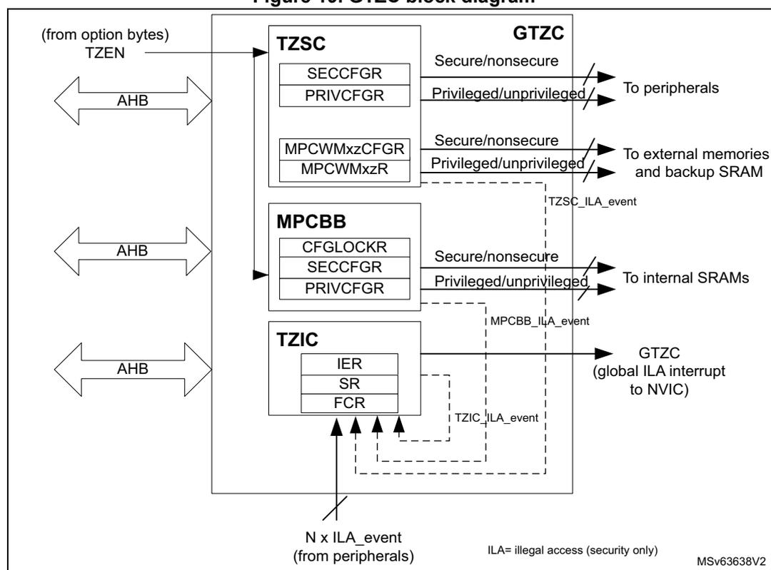
The diagram illustrates the internal architecture of the Global TrustZone Controller (GTZC). It is composed of three primary sub-blocks, each with its own AHB configuration port:
- TZSC (TrustZone Security Controller): Contains registers SECCFGR, PRIVCFGR, MPCWMxzCFGR, and MPCWMxzR. It outputs 'Secure/nonsecure' and 'Privileged/unprivileged' signals to peripherals and external memories/backup SRAM. It also generates 'TZSC_ILA_event' signals.
- MPCBB (Memory Protection Controller): Contains registers CFGLOCKR, SECCFGR, and PRIVCFGR. It outputs 'Secure/nonsecure' and 'Privileged/unprivileged' signals to internal SRAMs. It also generates 'MPCBB_ILA_event' signals.
- TZIC (TrustZone Interrupt Controller): Contains registers IER, SR, and FCR. It receives 'N x ILA_event (from peripherals)' and generates a 'GTZC (global ILA interrupt to NVIC)'. It also generates 'TZIC_ILA_event' signals.
The GTZC block is connected to various system components via AHB configuration ports. The legend indicates that 'ILA= illegal access (security only)'. The diagram is labeled 'MSV63638V2'.
5.4.2 Illegal access definition
Three different types of illegal access exist:
- • Illegal nonsecure access
Any nonsecure transaction trying to write a secure resource is considered as illegal and thus the addressed resource generates an illegal access interrupt for illegal write access and a bus error for illegal fetch access. However some exceptions exist on secure and privileged configuration registers: these later ones authorize nonsecure read access to secure registers (see GTZC_TZSC_SECCFGRx and GTZC_TZSC_PRIVCFGRx).
- • Illegal secure access
Any secure transaction trying to access nonsecure block in internal block-based SRAM or watermarked memory is considered as illegal.
Correct TZIC settings allows the capture of the associated event and then generates the GTZC_IRQn interrupt to the NVIC. This applies for read, write and execute access.
Concerning the MPCBB controller, there is an option to ignore secure data read/write access on nonsecure SRAM blocks, by setting the SRWILADIS bit in the GTZC_MPCBBz_CR register. Secure read and write data transactions are then allowed on nonsecure SRAM blocks, while secure execution access remains not allowed.
Any secure execute transaction trying to access a nonsecure peripheral register is considered as illegal and generate a bus error.
- • Illegal unprivileged access
Any unprivileged transaction trying to access a privileged resource is considered as illegal. There is no illegal access event generated for illegal read and write access. The addressed resource follows a silent-fail behavior, returning all zero data for read and ignoring any write. No bus error is generated. A bus error is generated when any unprivileged execute transaction tries to access a privileged memory.
5.4.3 TrustZone security controller (TZSC)
The TZSC is composed of a configurable set of registers, providing the following features:
- • Control of secure and privileged state for all peripherals, done through:
- – GTZC_TZSC_SECCFGRx registers to control AHB/APB firewall stubs for the securable peripherals
- – GTZC_TZSC_PRIVCFGRx registers to control AHB/APB firewall stubs for the privileged peripherals
- • For watermark memory protection controller (external memories and backup SRAM), two independent regions can be defined and the following fields are used to program:
- – the start of the first protected sub-region on external memory/backup SRAM: SUBA_START[10:0]
- – the length of the first protected sub-region on external memory/backup SRAM: SUBA_LENGTH[11:0]
- – the start of the second protected sub-region on external memory/backup SRAM: SUBB_START[10:0]
- – the length of the second protected sub-region on external memory/backup SRAM: SUBB_LENGTH[11:0]
A control register for each sub-region can be used to enable/disable the watermark memory protection controller as well as defining the right attributes of each sub-region.
Figure 20. Watermark memory protection controller (region x/sub-regions A and B)
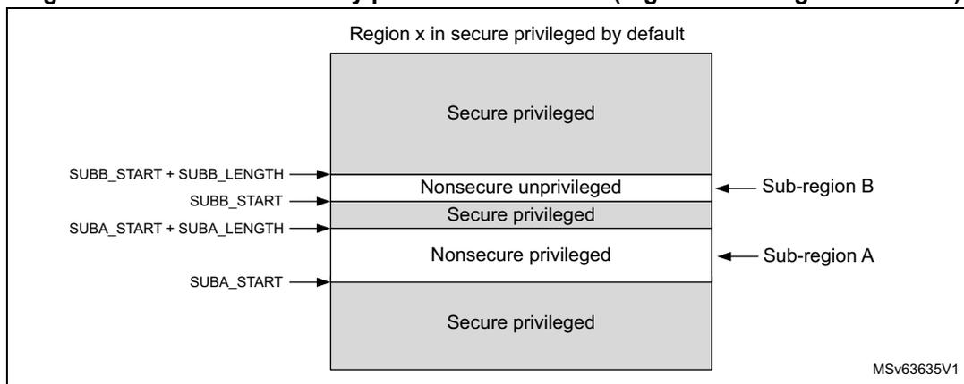
The diagram illustrates the memory protection configuration for region x and its sub-regions A and B. Region x is shown as a large box labeled "Region x in secure privileged by default". Inside this box, there are several horizontal segments representing different privilege levels:
- A top segment labeled "Secure privileged".
- A segment labeled "Nonsecure unprivileged". To its left, an arrow points to its top boundary with the label "SUBB_START + SUBB_LENGTH". To its right, an arrow points to it with the label "Sub-region B".
- A segment labeled "Secure privileged". To its left, an arrow points to its top boundary with the label "SUBB_START".
- A segment labeled "Nonsecure privileged". To its left, an arrow points to its top boundary with the label "SUBA_START + SUBA_LENGTH". To its right, an arrow points to it with the label "Sub-region A".
- A bottom segment labeled "Secure privileged". To its left, an arrow points to its top boundary with the label "SUBA_START".
In the figure above, region x represents the external memory or backup SRAM region (such as FSMC bank, OCTOSPI1, OCTOSPI2, HSPI1 or BKPSRAM). Secure and privileged attributes of sub-regions A and B are independently configurable. When no sub-regions are defined or enabled on the region x, then the default attribute of the region x is set as “secure-privileged”.
The tables below describe the secure/privileged properties of the common area of sub-region A and B when an overlapNonsecure exists.
Table 36. Secure properties of sub-regions A and B
| Sub-region A | Sub-region B | Properties of overlapped region A and B |
|---|---|---|
| Nonsecure | Nonsecure | Nonsecure |
| Nonsecure | Secure | Nonsecure |
| Secure | Nonsecure | Nonsecure |
| Secure | Secure | Secure |
Table 37. Privileged properties of sub-regions A and B
| Sub-region A | Sub-region B | Properties of overlapped region A and B |
|---|---|---|
| Unprivileged | Unprivileged | Unprivileged |
| Unprivileged | Privileged | Unprivileged |
| Privileged | Unprivileged | Unprivileged |
| Privileged | Privileged | Privileged |
5.4.4 Memory protection controller - block based (MPCBB)
The MPCBB is composed of a configurable set of registers allowing to define security and privileged policy for internal SRAM memories. The security and privileged policy can be individually configured per each 512-byte block of SRAM.
Figure 21. MPCBB block diagram
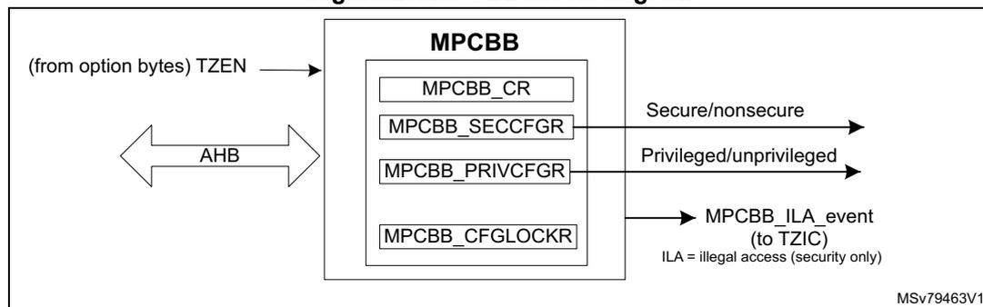
In order to setup the MPCBB, the following actions are needed (for example at boot time):
- • Secure firmware must define which memory blocks are secure by setting the correct bits in GTZC_MPCBBz_SECCFGRx.
- • Privileged firmware must define which memory blocks are privileged by setting the correct bits in GTZC_MPCBBz_PRIVCFGRx.
A MPCBB super-block is made of 32 consecutive blocks. For each super-block, secure application can lock all related security/privileged bits using the correct bits in GTZC_MPCBBz_CFGLOCKR1/2. This lock remains active until the next system reset.
Note: The block size is 512 bytes. The super-block size is \( 512 * 32 = 16 \) Kbytes.
5.4.5 TrustZone illegal access controller (TZIC)
The TZIC concentrates all illegal access source events. It is used only when the system is TrustZone enabled (TZEN = 1).
TZIC allows the trace (flag) of which event triggered the secure illegal access interrupt. Register masks (GTZC_TZIC_IERx) are available to filter unwanted event. On unmasked illegal event, TZIC generates the GTZC_IRQn interrupt to the NVIC.
For each illegal event source, a status flag and a clear bit exist (respectively within GTZC_TZIC_SRx and GTZC_TZIC_FCRx). The reset value of mask registers (GTZC_TZIC_IERx) is such that all events are masked.
5.4.6 Power-on/reset state
The power-on and reset state of the TZSC clear to 0 all bits of GTZC_TZSC_SECCFGRx and GTZC_TZSC_PRIVCFGRx, meaning that all securable peripherals are respectively set to nonsecure and unprivileged.
For internal SRAMx (x = 1 to 6), all GTZC_MPCBBz_SECCFGRx and GTZC_MPCBBz_PRIVCFGRx are set:
- • to 0xFFFF FFFF, making these internal memories block secure and privileged by default when TrustZone security is enabled at system level (TZEN = 1).
- to 0x0000 0000, making these internal memories block nonsecure and unprivileged by default when TrustZone security is disabled at system level (TZEN = 0)
For external memories and backup SRAM:
- all GTZC_TZSC_MPCWMxzR registers are set to 0x0000 0000, making these memories secure and privileged by default when TrustZone security is enabled at system level (TZEN = 1).
- GTZC_TZSC_MPCWMxzR registers are not accessible, and these memories are nonsecure and non-privileged by default when TrustZone security is disabled at system level (TZEN = 0).
Secure boot code can then program the security settings, making components secure or not as needed.
5.5 GTZC interrupts
TZIC is a secure peripheral, thus it systematically generates an illegal access event when accessed by a nonsecure access. The MPCBB and TZSC are TrustZone-aware peripherals, meaning that secure and nonsecure registers co-exist within the peripheral.
Table 38. GTZC interrupt request
| Interrupt acronym | Interrupt event | Event flag | Enable control bit | Interrupt clear method | Exit Sleep mode | Exit Stop mode | Exit Standby mode |
|---|---|---|---|---|---|---|---|
| GTZC | Illegal access | All flags in GTZC_TZIC_SRx | All bits in GTZC_TZIC_IERx | Write 1 in the bit GTZC_TZIC_FCRx | Yes | Yes | No |
5.6 GTZC1 TZSC registers
All registers are accessed only by words (32-bit).
5.6.1 GTZC1 TZSC control register (GTZC1_TZSC_CR)
Address offset: 0x000
Reset value: 0x0000 0000
Secure privileged access only.
| 31 | 30 | 29 | 28 | 27 | 26 | 25 | 24 | 23 | 22 | 21 | 20 | 19 | 18 | 17 | 16 |
| Res. | Res. | Res. | Res. | Res. | Res. | Res. | Res. | Res. | Res. | Res. | Res. | Res. | Res. | Res. | Res. |
| 15 | 14 | 13 | 12 | 11 | 10 | 9 | 8 | 7 | 6 | 5 | 4 | 3 | 2 | 1 | 0 |
| Res. | Res. | Res. | Res. | Res. | Res. | Res. | Res. | Res. | Res. | Res. | Res. | Res. | Res. | Res. | LCK rs |
Bits 31:1 Reserved, must be kept at reset value.
Bit 0 LCK : lock the configuration of GTZC1_TZSC_SECCFGRx and GTZC1_TZSC_PRIVCFGRx registers until next reset
This bit is cleared by default and once set, it can not be reset until system reset.
0: configuration of all GTZC1_TZSC_SECCFGRx and GTZC1_TZSC_PRIVCFGRx registers not locked
1: configuration of all GTZC1_TZSC_SECCFGRx and GTZC1_TZSC_PRIVCFGRx registers locked
5.6.2 GTZC1 TZSC secure configuration register 1 (GTZC1_TZSC_SECCFGR1)
Address offset: 0x010
Reset value: 0x0000 0000
Write-secure access only.
This register can be written only by secure privileged transaction when corresponding GTZC1_TZSC_PRIVCFGR register signal is set to 1. If a given PRIV bit is not set, the equivalent SEC bit can be written by secure unprivileged transaction.
Read accesses are authorized for any type of transactions, secure or not, privileged or not.
| 31 | 30 | 29 | 28 | 27 | 26 | 25 | 24 | 23 | 22 | 21 | 20 | 19 | 18 | 17 | 16 |
|---|---|---|---|---|---|---|---|---|---|---|---|---|---|---|---|
| Res. | Res. | Res. | Res. | Res. | Res. | Res. | Res. | I2C6SEC C | I2C5SEC C | USART6SEC | Res. | UCPD1SEC | FDCAN1SEC | LPTIM2SEC | I2C4SEC C |
| rw | rw | rw | rw | rw | rw | rw |
| 15 | 14 | 13 | 12 | 11 | 10 | 9 | 8 | 7 | 6 | 5 | 4 | 3 | 2 | 1 | 0 |
|---|---|---|---|---|---|---|---|---|---|---|---|---|---|---|---|
| CRSSEC C | I2C2SEC C | I2C1SEC C | UART5SEC | UART4SEC | USART3SEC | USART2SEC | SPI2SEC C | IWDGSEC EC | WWDGSEC | TIM7SEC EC | TIM6SEC EC | TIM5SEC EC | TIM4SEC EC | TIM3SEC EC | TIM2SEC EC |
| rw | rw | rw | rw | rw | rw | rw | rw | rw | rw | rw | rw | rw | rw | rw | rw |
Bits 31:24 Reserved, must be kept at reset value.
Bit 23 I2C6SEC : secure access mode for I2C6
0: nonsecure
1: secure
Note: This bit is only available on some devices in the STM32U5 series. Refer to the device datasheet for availability of its associated peripheral. If not present, consider this bit as reserved and kept at reset value.
Bit 22 I2C5SEC : secure access mode for I2C5
0: nonsecure
1: secure
Note: This bit is only available on some devices in the STM32U5 series. Refer to the device datasheet for availability of its associated peripheral. If not present, consider this bit as reserved and kept at reset value.
Bit 21 USART6SEC : secure access mode for USART6
0: nonsecure
1: secure
Note: This bit is only available on some devices in the STM32U5 series. Refer to the device datasheet for availability of its associated peripheral. If not present, consider this bit as reserved and kept at reset value.
Bit 20 Reserved, must be kept at reset value.
Bit 19 UCPD1SEC : secure access mode for UCPD1
0: nonsecure
1: secure
Note: This bit is only available on some devices in the STM32U5 series. Refer to the device datasheet for availability of its associated peripheral. If not present, consider this bit as reserved and kept at reset value.
Bit 18 FDCAN1SEC : secure access mode for FDCAN1
0: nonsecure
1: secure
Note: This bit is only available on some devices in the STM32U5 series. Refer to the device datasheet for availability of its associated peripheral. If not present, consider this bit as reserved and kept at reset value.
Bit 17 LPTIM2SEC : secure access mode for LPTIM2
0: nonsecure
1: secure
Bit 16 I2C4SEC : secure access mode for I2C4
0: nonsecure
1: secure
Bit 15 CRSSEC : secure access mode for CRS
0: nonsecure
1: secure
Bit 14 I2C2SEC : secure access mode for I2C2
0: nonsecure
1: secure
Bit 13 I2C1SEC : secure access mode for I2C1
0: nonsecure
1: secure
Bit 12 UART5SEC : secure access mode for UART5
0: nonsecure
1: secure
Bit 11 UART4SEC : secure access mode for UART4
0: nonsecure
1: secure
Bit 10 USART3SEC : secure access mode for USART3
0: nonsecure
1: secure
Bit 9 USART2SEC : secure access mode for USART2
0: nonsecure
1: secure
Note: This bit is only available on some devices in the STM32U5 series. Refer to the device datasheet for availability of its associated peripheral. If not present, consider this bit as reserved and kept at reset value.
Bit 8 SPI2SEC : secure access mode for SPI2
0: nonsecure
1: secure
- Bit 7
IWDGSEC
: secure access mode for IWDG
0: nonsecure
1: secure - Bit 6
WWDGSEC
: secure access mode for WWDG
0: nonsecure
1: secure - Bit 5
TIM7SEC
: secure access mode for TIM7
0: nonsecure
1: secure - Bit 4
TIM6SEC
: secure access mode for TIM6
0: nonsecure
1: secure - Bit 3
TIM5SEC
: secure access mode for TIM5
0: nonsecure
1: secure - Bit 2
TIM4SEC
: secure access mode for TIM4
0: nonsecure
1: secure - Bit 1
TIM3SEC
: secure access mode for TIM3
0: nonsecure
1: secure - Bit 0
TIM2SEC
: secure access mode for TIM2
0: nonsecure
1: secure
5.6.3 GTZC1 TZSC secure configuration register 2 (GTZC1_TZSC_SECCFGR2)
Address offset: 0x014
Reset value: 0x0000 0000
Write-secure access only.
This register can be written only by secure privileged transaction when corresponding GTZC1_TZSC_PRIVCFGR register signal is set to 1. If a given PRIV is not set, the equivalent SEC bit can be written by secure unprivileged transaction.
Read accesses are authorized for any type of transactions, secure or not, privileged or not.
| 31 | 30 | 29 | 28 | 27 | 26 | 25 | 24 | 23 | 22 | 21 | 20 | 19 | 18 | 17 | 16 |
|---|---|---|---|---|---|---|---|---|---|---|---|---|---|---|---|
| Res. | Res. | Res. | Res. | Res. | Res. | Res. | Res. | Res. | Res. | Res. | Res. | Res. | Res. | Res. | Res. |
| 15 | 14 | 13 | 12 | 11 | 10 | 9 | 8 | 7 | 6 | 5 | 4 | 3 | 2 | 1 | 0 |
| Res. | Res. | Res. | Res. | GFXTI MSEC | DSISE C | LTDCU SBSEC | SAI2SE C | SAI1SE C | TIM17S EC | TIM16S EC | TIM15S EC | USART 1SEC | TIM8S EC | SPI1SE C | TIM1S EC |
| rw | rw | rw | rw | rw | rw | rw | rw | rw | rw | rw | rw |
Bits 31:12 Reserved, must be kept at reset value.
Bit 11 GFXTIMSEC : secure access mode for GFXTIM
0: nonsecure
1: secure
Note: This bit is only available on some devices in the STM32U5 series. Refer to the device datasheet for availability of its associated peripheral. If not present, consider this bit as reserved and kept at reset value.
Bit 10 DSISEC : secure access mode for DSI
0: nonsecure
1: secure
Note: This bit is only available on some devices in the STM32U5 series. Refer to the device datasheet for availability of its associated peripheral. If not present, consider this bit as reserved and kept at reset value.
Bit 9 LTDCUSBSEC : secure access mode for LTDC or USB
0: nonsecure
1: secure
Note: This bit is secure for the LTDC on STM32U59x/5Ax/5Fx/5Gx. It is secure for the USB on STM32U535/545. It is reserved on STM32U575/585.
Bit 8 SAI2SEC : secure access mode for SAI2
0: nonsecure
1: secure
Note: This bit is only available on some devices in the STM32U5 series. Refer to the device datasheet for availability of its associated peripheral. If not present, consider this bit as reserved and kept at reset value.
Bit 7 SAI1SEC : secure access mode for SAI1
0: nonsecure
1: secure
Bit 6 TIM17SEC : secure access mode for TIM7
0: nonsecure
1: secure
Bit 5 TIM16SEC : secure access mode for TIM6
0: nonsecure
1: secure
Bit 4 TIM15SEC : secure access mode for TIM5
0: nonsecure
1: secure
Bit 3 USART1SEC : secure access mode for USART1
0: nonsecure
1: secure
Bit 2 TIM8SEC : secure access mode for TIM8
0: nonsecure
1: secure
Bit 1 SPI1SEC : secure access mode for SPI1
0: nonsecure
1: secure
Bit 0 TIM1SEC : secure access mode for TIM1
0: nonsecure
1: secure
5.6.4 GTZC1 TZSC secure configuration register 3 (GTZC1_TZSC_SECCFGR3)
Address offset: 0x018
Reset value: 0x0000 0000
Write-secure access only.
This register can be written only by secure privileged transaction when corresponding GTZC1_TZSC_PRIVCFGR register signal is set to 1. If a given PRIV is not set, the equivalent SEC bit can be written by secure unprivileged transaction.
Read accesses are authorized for any type of transactions, secure or not, privileged or not.
| 31 | 30 | 29 | 28 | 27 | 26 | 25 | 24 | 23 | 22 | 21 | 20 | 19 | 18 | 17 | 16 |
|---|---|---|---|---|---|---|---|---|---|---|---|---|---|---|---|
| Res. | Res. | Res. | JPEGSEC EC | DCACHE2_R EGSEC | HSPI1_ REGSEC C | GFXM MU_RE GSEC | GFXM MUSE C | GPU2D SEC | RAMC FGSEC | OCTOS PI2_RE GSEC | OCTOS PI1_RE GSEC | FSMC REGSEC C | SDMM C2SEC | SDMM C1SEC | OCTOS PIMSE C |
| rw | rw | rw | rw | rw | rw | rw | rw | rw | rw | rw | rw | rw |
| 15 | 14 | 13 | 12 | 11 | 10 | 9 | 8 | 7 | 6 | 5 | 4 | 3 | 2 | 1 | 0 |
|---|---|---|---|---|---|---|---|---|---|---|---|---|---|---|---|
| SAESS EC | PKASE C | RNGS EC | HASHS EC | AESSE C | OTGSE C | DCMIS EC | ADC12 SEC | DCACHE HE1_R EGSEC | ICACHE E_REG SEC | DMA2D SEC | TSCSE C | CRCSE C | FMACS EC | CORDI CSEC | MDF1S EC |
| rw | rw | rw | rw | rw | rw | rw | rw | rw | rw | rw | rw | rw | rw | rw | rw |
Bits 31:29 Reserved, must be kept at reset value.
Bit 28 JPEGSEC : secure access mode for JPEG
0: nonsecure
1: secure
Note: This bit is only available on some devices in the STM32U5 series. Refer to the device datasheet for availability of its associated peripheral. If not present, consider this bit as reserved and kept at reset value.
Bit 27 DCACHE2_REGSEC : secure access mode for DCACHE2 registers
0: nonsecure
1: secure
Note: This bit is only available on some devices in the STM32U5 series. Refer to the device datasheet for availability of its associated peripheral. If not present, consider this bit as reserved and kept at reset value.
Bit 26 HSPI1_REGSEC : secure access mode for HSPI1 registers
0: nonsecure
1: secure
Note: This bit is only available on some devices in the STM32U5 series. Refer to the device datasheet for availability of its associated peripheral. If not present, consider this bit as reserved and kept at reset value.
Bit 25 GFXMMU_REGSEC : secure access mode for GFXMMU registers
0: nonsecure
1: secure
Note: This bit is only available on some devices in the STM32U5 series. Refer to the device datasheet for availability of its associated peripheral. If not present, consider this bit as reserved and kept at reset value.
Bit 24 GFXMMUSEC : secure access mode for GFXMMU
0: nonsecure
1: secure
Note: This bit is only available on some devices in the STM32U5 series. Refer to the device datasheet for availability of its associated peripheral. If not present, consider this bit as reserved and kept at reset value.
Bit 23 GPU2DSEC : secure access mode for GPU2D
0: nonsecure
1: secure
Note: This bit is only available on some devices in the STM32U5 series. Refer to the device datasheet for availability of its associated peripheral. If not present, consider this bit as reserved and kept at reset value.
Bit 22 RAMCFGSEC : secure access mode for RAMCFG
0: nonsecure
1: secure
Bit 21 OCTOSPI2_REGSEC : secure access mode for OCTOSPI2 registers
0: nonsecure
1: secure
Note: This bit is only available on some devices in the STM32U5 series. Refer to the device datasheet for availability of its associated peripheral. If not present, consider this bit as reserved and kept at reset value.
Bit 20 OCTOSPI1_REGSEC : secure access mode for OCTOSPI1 registers
0: nonsecure
1: secure
Bit 19 FSMC_REGSEC : secure access mode for FSMC registers
0: nonsecure
1: secure
Note: This bit is only available on some devices in the STM32U5 series. Refer to the device datasheet for availability of its associated peripheral. If not present, consider this bit as reserved and kept at reset value.
Bit 18 SDMMC2SEC : secure access mode for SDMMC1
0: nonsecure
1: secure
Note: This bit is only available on some devices in the STM32U5 series. Refer to the device datasheet for availability of its associated peripheral. If not present, consider this bit as reserved and kept at reset value.
Bit 17 SDMMC1SEC : secure access mode for SDMMC2
0: nonsecure
1: secure
Bit 16 OCTOSPIMSEC : secure access mode for OCTOSPIM
0: nonsecure
1: secure
Note: This bit is only available on some devices in the STM32U5 series. Refer to the device datasheet for availability of its associated peripheral. If not present, consider this bit as reserved and kept at reset value.
Bit 15 SAESSEC : secure access mode for SAES
0: nonsecure
1: secure
Note: This bit is only available on some devices in the STM32U5 series. Refer to the device datasheet for availability of its associated peripheral. If not present, consider this bit as reserved and kept at reset value.
Bit 14 PKASEC : secure access mode for PKA
0: nonsecure
1: secure
Note: This bit is only available on some devices in the STM32U5 series. Refer to the device datasheet for availability of its associated peripheral. If not present, consider this bit as reserved and kept at reset value.
Bit 13 RNGSEC : secure access mode for RNG
0: nonsecure
1: secure
Bit 12 HASHSEC : secure access mode for HASH
0: nonsecure
1: secure
Bit 11 AESSEC : secure access mode for AES
0: nonsecure
1: secure
Note: This bit is only available on some devices in the STM32U5 series. Refer to the device datasheet for availability of its associated peripheral. If not present, consider this bit as reserved and kept at reset value.
Bit 10 OTGSEC : secure access mode for OTG_FS or OTG_HS
0: nonsecure
1: secure
Note: This bit is only available on some devices in the STM32U5 series. Refer to the device datasheet for availability of its associated peripheral. If not present, consider this bit as reserved and kept at reset value.
Bit 9 DCMISEC : secure access mode for DCMI and PSSI
0: nonsecure
1: secure
Bit 8 ADC12SEC : secure access mode for ADC1 and ADC2
0: nonsecure
1: secure
Bit 7 DCACHE1_REGSEC : secure access mode for DCACHE1 registers
0: nonsecure
1: secure
Bit 6 ICACHE_REGSEC : secure access mode for ICACHE registers
0: nonsecure
1: secure
Bit 5 DMA2DSEC : secure access mode for register of DMA2D
0: nonsecure
1: secure
Note: This bit is only available on some devices in the STM32U5 series. Refer to the device datasheet for availability of its associated peripheral. If not present, consider this bit as reserved and kept at reset value.
Bit 4 TSCSEC : secure access mode for TSC
0: nonsecure
1: secure
Bit 3 CRCSEC : secure access mode for CRC
0: nonsecure
1: secure
Bit 2 FMACSEC : secure access mode for FMAC
0: nonsecure
1: secure
Bit 1 CORDICSEC : secure access mode for CORDIC
0: nonsecure
1: secure
Bit 0 MDF1SEC : secure access mode for MDF1
0: nonsecure
1: secure
5.6.5 GTZC1 TZSC privilege configuration register 1 (GTZC1_TZSC_PRIVCFG1)
Address offset: 0x020
Reset value: 0x0000 0000
Write-privileged access only.
This register can be read or written only by secure privileged transaction when corresponding GTZC1_TZSC_SECCFG register signal is set to 1. If a given SEC bit is not set, the equivalent PRIV bit can be read/written by nonsecure privileged transaction.
Read accesses are authorized for any type of transactions, secure or not, privileged or not.
| 31 | 30 | 29 | 28 | 27 | 26 | 25 | 24 | 23 | 22 | 21 | 20 | 19 | 18 | 17 | 16 |
|---|---|---|---|---|---|---|---|---|---|---|---|---|---|---|---|
| Res. | Res. | Res. | Res. | Res. | Res. | Res. | Res. | I2C6PR IV | I2C5PR IV | USART 6PRIV | Res. | UCPD1 PRIV | FDCAN 1PRIV | LPTIM2 PRIV | I2C4PR IV |
| rw | rw | rw | rw | rw | rw | rw | |||||||||
| 15 | 14 | 13 | 12 | 11 | 10 | 9 | 8 | 7 | 6 | 5 | 4 | 3 | 2 | 1 | 0 |
| CRSPR IV | I2C2PR IV | I2C1PR IV | UART5 PRIV | UART4 PRIV | USART 3PRIV | USART 2PRIV | SPI2P RIV | IWDGP RIV | WWDG PRIV | TIM7P RIV | TIM6P RIV | TIM5P RIV | TIM4P RIV | TIM3P RIV | TIM2P RIV |
| rw | rw | rw | rw | rw | rw | rw | rw | rw | rw | rw | rw | rw | rw | rw | rw |
Bits 31:24 Reserved, must be kept at reset value.
Bit 23 I2C6PRIV : privileged access mode for I2C6
0: unprivileged
1: privileged
Note: This bit is only available on some devices in the STM32U5 series. Refer to the device datasheet for availability of its associated peripheral. If not present, consider this bit as reserved and kept at reset value.
Bit 22 I2C5PRIV : privileged access mode for I2C5
0: unprivileged
1: privileged
Note: This bit is only available on some devices in the STM32U5 series. Refer to the device datasheet for availability of its associated peripheral. If not present, consider this bit as reserved and kept at reset value.
Bit 21 USART6PRIV : privileged access mode for USART6
0: unprivileged
1: privileged
Note: This bit is only available on some devices in the STM32U5 series. Refer to the device datasheet for availability of its associated peripheral. If not present, consider this bit as reserved and kept at reset value.
Bit 20 Reserved, must be kept at reset value.
Bit 19 UCPD1PRIV : privileged access mode for UCPD1
0: unprivileged
1: privileged
Note: This bit is only available on some devices in the STM32U5 series. Refer to the device datasheet for availability of its associated peripheral. If not present, consider this bit as reserved and kept at reset value.
Bit 18 FDCAN1PRIV : privileged access mode for FDCAN1
0: unprivileged
1: privileged
Note: This bit is only available on some devices in the STM32U5 series. Refer to the device datasheet for availability of its associated peripheral. If not present, consider this bit as reserved and kept at reset value.
Bit 17 LPTIM2PRIV : privileged access mode for LPTIM2
0: unprivileged
1: privileged
Bit 16 I2C4PRIV : privileged access mode for I2C4
0: unprivileged
1: privileged
Bit 15 CRSPRIV : privileged access mode for CRS
0: unprivileged
1: privileged
Bit 14 I2C2PRIV : privileged access mode for I2C2
0: unprivileged
1: privileged
Bit 13 I2C1PRIV : privileged access mode for I2C1
0: unprivileged
1: privileged
Bit 12 UART5PRIV : privileged access mode for UART5
0: unprivileged
1: privileged
Bit 11 UART4PRIV : privileged access mode for UART4
0: unprivileged
1: privileged
Bit 10 USART3PRIV : privileged access mode for USART3
0: unprivileged
1: privileged
Bit 9 USART2PRIV : privileged access mode for USART2
0: unprivileged
1: privileged
Note: This bit is only available on some devices in the STM32U5 series. Refer to the device datasheet for availability of its associated peripheral. If not present, consider this bit as reserved and kept at reset value.
Bit 8 SPI2PRIV : privileged access mode for SPI2
0: unprivileged
1: privileged
Bit 7 IWDGPRIV : privileged access mode for IWDG
0: unprivileged
1: privileged
Bit 6 WWDGPRIV : privileged access mode for WWDG
0: unprivileged
1: privileged
Bit 5 TIM7PRIV : privileged access mode for TIM7
0: unprivileged
1: privileged
Bit 4 TIM6PRIV : privileged access mode for TIM6
0: unprivileged
1: privileged
Bit 3 TIM5PRIV : privileged access mode for TIM5
0: unprivileged
1: privileged
Bit 2 TIM4PRIV : privileged access mode for TIM4
0: unprivileged
1: privileged
Bit 1 TIM3PRIV : privileged access mode for TIM3
0: unprivileged
1: privileged
Bit 0 TIM2PRIV : privileged access mode for TIM2
0: unprivileged
1: privileged
5.6.6 GTZC1 TZSC privilege configuration register 2 (GTZC1_TZSC_PRIVCFGR2)
Address offset: 0x024
Reset value: 0x0000 0000
Write-privileged access only.
This register can be read or written only by secure privileged transaction when corresponding GTZC1_TZSC_SECCFGR register signal is set to 1. If a given SEC bit is not set, the equivalent PRIV bit can be read/written by nonsecure privileged transaction.
Read accesses are authorized for any type of transactions, secure or not, privileged or not.
| 31 | 30 | 29 | 28 | 27 | 26 | 25 | 24 | 23 | 22 | 21 | 20 | 19 | 18 | 17 | 16 |
|---|---|---|---|---|---|---|---|---|---|---|---|---|---|---|---|
| Res. | Res. | Res. | Res. | Res. | Res. | Res. | Res. | Res. | Res. | Res. | Res. | Res. | Res. | Res. | Res. |
| 15 | 14 | 13 | 12 | 11 | 10 | 9 | 8 | 7 | 6 | 5 | 4 | 3 | 2 | 1 | 0 |
| Res. | Res. | Res. | Res. | GFXTI MPriv | DSIPRI V | LTDCU SBPRI V | SAI2P RIV | SAI1P RIV | TIM17P RIV | TIM16P RIV | TIM15P RIV | USART 1PRIV | TIM8P RIV | SPI1P RIV | TIM1P RIV |
| rw | rw | rw | rw | rw | rw | rw | rw | rw | rw | rw | rw |
Bits 31:12 Reserved, must be kept at reset value.
Bit 11 GFXTIMPRIV : privileged access mode for GFXTIM
0: unprivileged
1: privileged
Note: This bit is only available on some devices in the STM32U5 series. Refer to the device datasheet for availability of its associated peripheral. If not present, consider this bit as reserved and kept at reset value.
Bit 10 DSIPRIV : privileged access mode for DSI
0: unprivileged
1: privileged
Note: This bit is only available on some devices in the STM32U5 series. Refer to the device datasheet for availability of its associated peripheral. If not present, consider this bit as reserved and kept at reset value.
Bit 9 LTDCUSBPRIV : privileged access mode for LTDC or USB
0: unprivileged
1: privileged
Note: This bit privileges the LTDC on STM32U59x/5Ax/5Fx/5Gx. It privileges the USB on STM32U535/545. It is reserved on STM32U575/585.
Bit 8 SAI2PRIV : privileged access mode for SAI2
0: unprivileged
1: privileged
Note: This bit is only available on some devices in the STM32U5 series. Refer to the device datasheet for availability of its associated peripheral. If not present, consider this bit as reserved and kept at reset value.
Bit 7 SAI1PRIV : privileged access mode for SAI1
0: unprivileged
1: privileged
- Bit 6
TIM17PRIV
: privileged access mode for TIM17
0: unprivileged
1: privileged - Bit 5
TIM16PRIV
: privileged access mode for TIM16
0: unprivileged
1: privileged - Bit 4
TIM15PRIV
: privileged access mode for TIM15
0: unprivileged
1: privileged - Bit 3
USART1PRIV
: privileged access mode for USART1
0: unprivileged
1: privileged - Bit 2
TIM8PRIV
: privileged access mode for TIM8
0: unprivileged
1: privileged - Bit 1
SPI1PRIV
: privileged access mode for SPI1PRIV
0: unprivileged
1: privileged - Bit 0
TIM1PRIV
: privileged access mode for TIM1
0: unprivileged
1: privileged
5.6.7 GTZC1 TZSC privilege configuration register 3 (GTZC1_TZSC_PRIVCFGR3)
Address offset: 0x028
Reset value: 0x0000 0000
Write-privileged access only.
This register can be read or written only by secure privileged transaction when corresponding GTZC1_TZSC_SECCFGR register signal is set to 1. If a given SEC bit is not set, the equivalent PRIV bit can be read/written by nonsecure privileged transaction.
Read accesses are authorized for any type of transactions, secure or not, privileged or not.
| 31 | 30 | 29 | 28 | 27 | 26 | 25 | 24 | 23 | 22 | 21 | 20 | 19 | 18 | 17 | 16 |
|---|---|---|---|---|---|---|---|---|---|---|---|---|---|---|---|
| Res. | Res. | Res. | JPEGP RIV | DCAC HE2_R EGPRI V | HSPI1_ REGP RIV | GFXM MU_RE GPRIV | GFXM MUPRI V | GPU2D PRIV | RAMC FGPRI V | OCTOS PI2_RE GPRIV | OCTOS PI1_RE GPRIV | FSMC_ REGP RIV | SDMM C2PRI V | SDMM C1PRI V | OCTOS PIMPRI V |
| rw | rw | rw | rw | rw | rw | rw | rw | rw | rw | rw | rw | rw | |||
| 15 | 14 | 13 | 12 | 11 | 10 | 9 | 8 | 7 | 6 | 5 | 4 | 3 | 2 | 1 | 0 |
| SAESP RIV | PKAPR IV | RNGP RIV | HASHP RIV | AESPR IV | OTGP RIV | DCMIP RIV | ADC12 PRIV | DCAC HE1_R EGPRI V | ICACH E_REG PRIV | DMA2D PRIV | TSCP RIV | CRCP RIV | FMACP RIV | CORDI CPRIV | MDF1P RIV |
| rw | rw | rw | rw | rw | rw | rw | rw | rw | rw | rw | rw | rw | rw | rw | rw |
Bits 31:29 Reserved, must be kept at reset value.
Bit 28 JPEGPRIV : privileged access mode for JPEG
0: unprivileged
1: privileged
Note: This bit is only available on some devices in the STM32U5 series. Refer to the device datasheet for availability of its associated peripheral. If not present, consider this bit as reserved and kept at reset value.
Bit 27 DCACHE2_REGPRIV : privileged access mode for DCACHE2 registers
0: unprivileged
1: privileged
Note: This bit is only available on some devices in the STM32U5 series. Refer to the device datasheet for availability of its associated peripheral. If not present, consider this bit as reserved and kept at reset value.
Bit 26 HSPI1_REGPRIV : privileged access mode for HSPI1 registers
0: unprivileged
1: privileged
Note: This bit is only available on some devices in the STM32U5 series. Refer to the device datasheet for availability of its associated peripheral. If not present, consider this bit as reserved and kept at reset value.
Bit 25 GFXMMU_REGPRIV : privileged access mode for GFXMMU registers
0: unprivileged
1: privileged
Note: This bit is only available on some devices in the STM32U5 series. Refer to the device datasheet for availability of its associated peripheral. If not present, consider this bit as reserved and kept at reset value.
Bit 24 GFXMMUPRIV : privileged access mode for GFXMMU
0: unprivileged
1: privileged
Note: This bit is only available on some devices in the STM32U5 series. Refer to the device datasheet for availability of its associated peripheral. If not present, consider this bit as reserved and kept at reset value.
Bit 23 GPU2DPRIV : privileged access mode for GPU2D
0: unprivileged
1: privileged
Note: This bit is only available on some devices in the STM32U5 series. Refer to the device datasheet for availability of its associated peripheral. If not present, consider this bit as reserved and kept at reset value.
Bit 22 RAMCFGPRIV : privileged access mode for RAMCFG
0: unprivileged
1: privileged
Bit 21 OCTOSPI2_REGPRIV : privileged access mode for OCTOSPI2
0: unprivileged
1: privileged
Note: This bit is only available on some devices in the STM32U5 series. Refer to the device datasheet for availability of its associated peripheral. If not present, consider this bit as reserved and kept at reset value.
Bit 20 OCTOSPI1_REGPRIV : privileged access mode for OCTOSPI1
0: unprivileged
1: privileged
Bit 19 FSMC_REGPRIV : privileged access mode for FSMC registers
0: unprivileged
1: privileged
Note: This bit is only available on some devices in the STM32U5 series. Refer to the device datasheet for availability of its associated peripheral. If not present, consider this bit as reserved and kept at reset value.
Bit 18 SDMMC2PRIV : privileged access mode for SDMMC1
0: unprivileged
1: privileged
Note: This bit is only available on some devices in the STM32U5 series. Refer to the device datasheet for availability of its associated peripheral. If not present, consider this bit as reserved and kept at reset value.
Bit 17 SDMMC1PRIV : privileged access mode for SDMMC2
0: unprivileged
1: privileged
Bit 16 OCTOSPIMPRIV : privileged access mode for OCTOSPIM
0: unprivileged
1: privileged
Note: This bit is only available on some devices in the STM32U5 series. Refer to the device datasheet for availability of its associated peripheral. If not present, consider this bit as reserved and kept at reset value.
Bit 15 SAESPRIV : privileged access mode for SAES
0: unprivileged
1: privileged
Note: This bit is only available on some devices in the STM32U5 series. Refer to the device datasheet for availability of its associated peripheral. If not present, consider this bit as reserved and kept at reset value.
Bit 14 PKAPRIV : privileged access mode for PKA
0: unprivileged
1: privileged
Note: This bit is only available on some devices in the STM32U5 series. Refer to the device datasheet for availability of its associated peripheral. If not present, consider this bit as reserved and kept at reset value.
Bit 13 RNGPRIV : privileged access mode for RNG
0: unprivileged
1: privileged
Bit 12 HASHPRIV : privileged access mode for HASH
0: unprivileged
1: privileged
Bit 11 AESPRIV : privileged access mode for AES
0: unprivileged
1: privileged
Note: This bit is only available on some devices in the STM32U5 series. Refer to the device datasheet for availability of its associated peripheral. If not present, consider this bit as reserved and kept at reset value.
Bit 10 OTGPRIV : privileged access mode for OTG_FS or OTG_HS
0: unprivileged
1: privileged
Note: This bit is only available on some devices in the STM32U5 series. Refer to the device datasheet for availability of its associated peripheral. If not present, consider this bit as reserved and kept at reset value.
Bit 9 DCMIPRIV : privileged access mode for DCMI and PSSI
0: unprivileged
1: privileged
Bit 8 ADC12PRIV : privileged access mode for ADC1 and ADC2
0: unprivileged
1: privileged
Bit 7 DCACHE1_REGPRIV : privileged access mode for DCACHE1 registers
0: unprivileged
1: privileged
Bit 6 ICACHE_REGPRIV : privileged access mode for ICACHE registers
0: unprivileged
1: privileged
Bit 5 DMA2DPRIV : privileged access mode for register of DMA2D
0: unprivileged
1: privileged
Note: This bit is only available on some devices in the STM32U5 series. Refer to the device datasheet for availability of its associated peripheral. If not present, consider this bit as reserved and kept at reset value.
Bit 4 TSCPRIV : privileged access mode for TSC
0: unprivileged
1: privileged
Bit 3 CRCPRIV : privileged access mode for CRC
0: unprivileged
1: privileged
Bit 2 FMACPRIV : privileged access mode for FMAC
0: unprivileged
1: privileged
Bit 1 CORDICPRIV : privileged access mode for CORDIC
0: unprivileged
1: privileged
Bit 0 MDF1PRIV : privileged access mode for MDF1
0: unprivileged
1: privileged
5.6.8 GTZC1 TZSC memory x sub-region z watermark configuration register (GTZC1_TZSC_MPCWMxzCFGR) (z = A to B)
Address offset: Block A: \( 0x40 + 0x10 * (x - 1) \) ( \( x = 1 \) to \( 6 \) )
Address offset: Block B: \( 0x48 + 0x10 * (x - 1) \) ( \( x = 1, 2, 5, 6 \) )
Reset value: \( 0x0000\ 0000 \)
Secure privilege access only.
Note: Some registers are only available on some devices in the STM32U5 series. Refer to the device datasheet for availability of its associated memory region.
| 31 | 30 | 29 | 28 | 27 | 26 | 25 | 24 | 23 | 22 | 21 | 20 | 19 | 18 | 17 | 16 |
|---|---|---|---|---|---|---|---|---|---|---|---|---|---|---|---|
| Res. | Res. | Res. | Res. | Res. | Res. | Res. | Res. | Res. | Res. | Res. | Res. | Res. | Res. | Res. | Res. |
| 15 | 14 | 13 | 12 | 11 | 10 | 9 | 8 | 7 | 6 | 5 | 4 | 3 | 2 | 1 | 0 |
| Res. | Res. | Res. | Res. | Res. | Res. | PRIV | SEC | Res. | Res. | Res. | Res. | Res. | Res. | SRLOCK | SREN |
| rw | rw | rs | rw |
Bits 31:10 Reserved, must be kept at reset value.
Bit 9 PRIV : Privileged sub-region z of base region x
This bit is taken into account only if SREN is set.
0: Privileged and unprivileged accesses are granted in sub-region z.
1: Only privileged accesses are granted in sub-region z of region x.
Bit 8 SEC : Secure sub-region z of base region x
This bit is taken into account only if SREN is set.
0: Only nonsecure data accesses are granted to sub-region z of region x.
1: Only secure data accesses are granted to sub-region z of region x.
Bits 7:2 Reserved, must be kept at reset value.
Bit 1 SRLOCK : Sub-region z lock
This bit, once set, can be cleared only by a system reset.
0: GTZC1_TZSC_MPCWMzCFGR, GTZC1_TZSC_MPCWMzAR and GTZC1_TZSC_MPCWMzBR can be written.
1: Writes to GTZC1_TZSC_MPCWMzCFGR, GTZC1_TZSC_MPCWMzAR and GTZC1_TZSC_MPCWMzBR are ignored.
Bit 0 SREN : Sub-region z enable
0: Sub-region z is disabled. Access control of base region x applies to any access between this sub-region start- and end-addresses.
1: Sub-region z of region x is enabled. Access control defined in GTZC1_TZSC_MPCWMzCFGR applies to any access between this sub-region start- and end-addresses, both defined in GTZC1_TZSC_MPCWMzAR and GTZC1_TZSC_MPCWMzBR.
Note: External memories that are watermark controlled start fully nonsecure/unprivileged at reset when TZEN = 0. When TZEN = 1, external memories start fully secure/fully privileged (inverted reset-value).
5.6.9 GTZC1 TZSC memory x sub-region A watermark register (GTZC1_TZSC_MPCWMxAR)
Address offset:
\(
0x44 + 0x10 * (x - 1)
\)
(
\(
x = 1
\)
to
\(
6
\)
)
Reset value:
\(
0x0000\ 0000
\)
Secure privilege access only.
When SUBA_START + SUBA_LENGTH is higher than the maximum size allowed for the memory, a saturation of SUBA_LENGTH is applied automatically.
When an overlap of sub-region A and B exists, secure/privileged attributes of both sub-regions apply on the common section (see Section 5.4.3 ).
Note: Some registers are only available on some devices in the STM32U5 Series. Refer to the device datasheet for availability of its associated memory region.
| 31 | 30 | 29 | 28 | 27 | 26 | 25 | 24 | 23 | 22 | 21 | 20 | 19 | 18 | 17 | 16 |
|---|---|---|---|---|---|---|---|---|---|---|---|---|---|---|---|
| Res. | Res. | Res. | Res. | SUBA_LENGTH[11:0] | |||||||||||
| rw | rw | rw | rw | rw | rw | rw | rw | rw | rw | rw | rw | ||||
| 15 | 14 | 13 | 12 | 11 | 10 | 9 | 8 | 7 | 6 | 5 | 4 | 3 | 2 | 1 | 0 |
| Res. | Res. | Res. | Res. | Res. | SUBA_START[10:0] | ||||||||||
| rw | rw | rw | rw | rw | rw | rw | rw | rw | rw | rw | |||||
Bits 31:28 Reserved, must be kept at reset value.
Bits 27:16 SUBA_LENGTH[11:0] : Length of sub-region A in region x
This field defines the length of the sub-region A, to be multiplied by the granularity defined in Table 31 .
When SUBA_START + SUBA_LENGTH is higher than the maximum size allowed for the memory, a saturation of SUBA_LENGTH is applied automatically.
If SUBA_LENGTH = 0, the sub-region A is disabled. (SREN bit in GTZC1_TZSC_MPCMWxACFGR is cleared).
Bits 15:11 Reserved, must be kept at reset value.
Bits 10:0 SUBA_START[10:0] : Start of sub-region A in region x
This field defines the address offset of the sub-region A, to be multiplied by the granularity defined in Table 31 , versus the start of the region x.
External memories that are watermark controlled, start fully nonsecure at reset when TZEN = 0. When TZEN = 1, external memories start fully secure (inverted reset-value).
5.6.10 GTZC1 TZSC memory x sub-region B watermark register (GTZC1_TZSC_MPCWMxBR)
Address offset: \( 0x4C + 0x10 * (x - 1) \) ( \( x = 1, 2, 5, 6 \) )
Reset value: 0x0000 0000
Secure privilege access only.
When SUBB_START + SUBB_LENGTH is higher than the maximum size allowed for the memory, a saturation of SUBB_LENGTH is applied automatically.
When an overlap of sub-region A and B exists, secure/privileged attributes of both sub-regions apply on the common section (see Section 5.4.3 ).
Note: Some registers are only available on some devices in the STM32U5 series. Refer to the device datasheet for availability of its associated memory region.
| 31 | 30 | 29 | 28 | 27 | 26 | 25 | 24 | 23 | 22 | 21 | 20 | 19 | 18 | 17 | 16 |
|---|---|---|---|---|---|---|---|---|---|---|---|---|---|---|---|
| Res. | Res. | Res. | Res. | SUBB_LENGTH[11:0] | |||||||||||
| rw | rw | rw | rw | rw | rw | rw | rw | rw | rw | rw | rw | ||||
| 15 | 14 | 13 | 12 | 11 | 10 | 9 | 8 | 7 | 6 | 5 | 4 | 3 | 2 | 1 | 0 |
| Res. | Res. | Res. | Res. | Res. | SUBB_START[10:0] | ||||||||||
| rw | rw | rw | rw | rw | rw | rw | rw | rw | rw | rw | |||||
Bits 31:28 Reserved, must be kept at reset value.
Bits 27:16
SUBB_LENGTH[11:0]
: Length of sub-region B in region x
This field defines the length of the sub-region B, to be multiplied by the granularity defined in
Table 31
.
When SUBB_START + SUBB_LENGTH is higher than the maximum size allowed for the memory, a saturation of SUBB_LENGTH is applied automatically.
If SUBB_LENGTH = 0, the sub-region B is disabled. (SREN bit in GTZC1_TZSC_MPCWMxBCFGR is cleared).
Bits 15:11 Reserved, must be kept at reset value.
Bits 10:0
SUBB_START[10:0]
: Start of sub-region B in region x
This field defines the address offset of the sub-region B, to be multiplied by the granularity defined in
Table 31
, versus the start of the region x.
External memories that are watermark controlled, start fully nonsecure at reset when TZEN = 0. When TZEN = 1, external memories start fully secure (inverted reset-value).
5.6.11 GTZC1 TZSC register map
Table 39. GTZC1 TZSC register map and reset values
| Offset | Register name | 31 | 30 | 29 | 28 | 27 | 26 | 25 | 24 | 23 | 22 | 21 | 20 | 19 | 18 | 17 | 16 | 15 | 14 | 13 | 12 | 11 | 10 | 9 | 8 | 7 | 6 | 5 | 4 | 3 | 2 | 1 | 0 |
|---|---|---|---|---|---|---|---|---|---|---|---|---|---|---|---|---|---|---|---|---|---|---|---|---|---|---|---|---|---|---|---|---|---|
| 0x000 | GTZC1_TZSC_CR | Res. | Res. | Res. | Res. | Res. | Res. | Res. | Res. | Res. | Res. | Res. | Res. | Res. | Res. | Res. | Res. | Res. | Res. | Res. | Res. | Res. | Res. | Res. | Res. | Res. | Res. | Res. | Res. | Res. | Res. | Res. | LOCK |
| Reset value | 0 | ||||||||||||||||||||||||||||||||
| 0x004-0x00C | Reserved | Reserved | |||||||||||||||||||||||||||||||
| 0x010 | GTZC1_TZSC_SECCFGR1 | Res. | Res. | Res. | Res. | Res. | Res. | Res. | Res. | I2C6SEC | I2C5SEC | USART6SEC | Res. | UCPD1SEC | FDCAN1SEC | LPTIM2SEC | I2C4SEC | CRSSEC | I2C2SEC | I2C1SEC | UART5SEC | UART4SEC | USART3SEC | USART2SEC | SPI2SEC | IWDGSEC | WWDGSEC | TIM7SEC | TIM6SEC | TIM5SEC | TIM4SEC | TIM3SEC | TIM2SEC |
| Reset value | 0 | 0 | 0 | 0 | 0 | 0 | 0 | 0 | 0 | 0 | 0 | 0 | 0 | 0 | 0 | 0 | 0 | 0 | 0 | 0 | 0 | 0 | 0 | ||||||||||
Table 39. GTZC1 TZSC register map and reset values (continued)
| Offset | Register name | 31 | 30 | 29 | 28 | 27 | 26 | 25 | 24 | 23 | 22 | 21 | 20 | 19 | 18 | 17 | 16 | 15 | 14 | 13 | 12 | 11 | 10 | 9 | 8 | 7 | 6 | 5 | 4 | 3 | 2 | 1 | 0 | |
|---|---|---|---|---|---|---|---|---|---|---|---|---|---|---|---|---|---|---|---|---|---|---|---|---|---|---|---|---|---|---|---|---|---|---|
| 0x014 | GTZC1_TZSC_ SECCFGR2 | Res. | Res. | Res. | Res. | Res. | Res. | Res. | Res. | Res. | Res. | Res. | Res. | Res. | Res. | Res. | Res. | Res. | Res. | Res. | Res. | GFXTMSEC | DSISEC | LTDCUSBSEC | SAI2SEC | SAI1SEC | TIM17SEC | TIM16SEC | TIM15SEC | USART1SEC | TIM8SEC | SPI1SEC | TIM1SEC | |
| Reset value | 0 | 0 | 0 | 0 | 0 | 0 | 0 | 0 | 0 | 0 | 0 | 0 | ||||||||||||||||||||||
| 0x018 | GTZC1_TZSC_ SECCFGR3 | Res. | Res. | Res. | JPEGSEC | DCACHE2_REGSEC | HSPI1_REGSEC | GFXMMU_REGSEC | GFXMMUSEC | GPU2DSEC | RAMCFGSEC | OCTOSPI2_REGSEC | OCTOSPI1_REGSEC | FSMC_REGSEC | SDMMC2SEC | SDMMC1SEC | OCTOSPIMSEC | SAESSEC | PKASEC | RNGSEC | HASHSEC | AESSEC | OTGSEC | DCMSEC | ADC12SEC | DCACHE1_REGSEC | ICACHE_REGSEC | DMA2DSEC | TSCSEC | CRCSEC | FMACSEC | CORDICSEC | MDF1SEC | |
| Reset value | 0 | 0 | 0 | 0 | 0 | 0 | 0 | 0 | 0 | 0 | 0 | 0 | 0 | 0 | 0 | 0 | 0 | 0 | 0 | 0 | 0 | 0 | 0 | 0 | 0 | 0 | 0 | 0 | 0 | |||||
| 0x01C | Reserved | Reserved | ||||||||||||||||||||||||||||||||
| 0x020 | GTZC1_TZSC_ PRIVCFGGR1 | Res. | Res. | Res. | Res. | Res. | Res. | Res. | Res. | I2C6PRIV | I2C5PRIV | USART6PRIV | Res. | UCPD1PRIV | FDCAN1PRIV | LPTIM2PRIV | I2C4PRIV | CRSPRIV | I2C2PRIV | I2C1PRIV | UART5PRIV | UART4PRIV | USART3PRIV | USART2PRIV | SPI2PRIV | IWDGPRIV | WWDGPRIV | TIM7PRIV | TIM6PRIV | TIM5PRIV | TIM4PRIV | TIM3PRIV | TIM2PRIV | |
| Reset value | 0 | 0 | 0 | 0 | 0 | 0 | 0 | 0 | 0 | 0 | 0 | 0 | 0 | 0 | 0 | 0 | 0 | 0 | 0 | 0 | 0 | 0 | 0 | |||||||||||
| 0x024 | GTZC1_TZSC_ PRIVCFGGR2 | Res. | Res. | Res. | Res. | Res. | Res. | Res. | Res. | Res. | Res. | Res. | Res. | Res. | Res. | Res. | Res. | Res. | Res. | Res. | Res. | GFXTMPRIV | DSIPRIV | LTDCUSBPRIV | SAI2PRIV | SAI1PRIV | TIM17PRIV | TIM16PRIV | TIM15PRIV | USART1PRIV | TIM8PRIV | SPI1PRIV | TIM1PRIV | |
| Reset value | 0 | 0 | 0 | 0 | 0 | 0 | 0 | 0 | 0 | 0 | 0 | 0 | ||||||||||||||||||||||
| 0x028 | GTZC1_TZSC_ PRIVCFGGR3 | Res. | Res. | Res. | JPEGPRIV | DCACHE2_REGPRIV | HSPI1_REGPRIV | GFXMMU_REGPRIV | GFXMMUPRIV | GPU2DPRIV | RAMCFGPRIV | OCTOSPI2_REGPRIV | OCTOSPI1_REGPRIV | FSMC_REGPRIV | SDMMC2PRIV | SDMMC1PRIV | OCTOSPIMPRIV | SAESPRIV | PKAPRIV | RNGPRIV | HASHPRIV | AESPRIV | OTGPRIV | DCMIPRIV | ADC12PRIV | DCACHE1_REGPRIV | ICACHE_REGPRIV | DMA2DPRIV | TSCPRIV | CRCPRIV | FMACPRIV | CORDICPRIV | MDF1PRIV | |
| Reset value | 0 | 0 | 0 | 0 | 0 | 0 | 0 | 0 | 0 | 0 | 0 | 0 | 0 | 0 | 0 | 0 | 0 | 0 | 0 | 0 | 0 | 0 | 0 | 0 | 0 | 0 | 0 | 0 | 0 | |||||
| 0x02C- 0x03C | Reserved | Reserved | ||||||||||||||||||||||||||||||||
| 0x040 | GTZC1_TZSC_ MPCWM1ACFGR | Res. | Res. | Res. | Res. | Res. | Res. | Res. | Res. | Res. | Res. | Res. | Res. | Res. | Res. | Res. | Res. | Res. | Res. | Res. | Res. | Res. | PRIV | SEC | Res. | Res. | Res. | Res. | Res. | Res. | Res. | Res. | SRLOCK | SREN |
| Reset value | 0 | 0 | 0 | 0 | ||||||||||||||||||||||||||||||
| 0x044 | GTZC1_TZSC_ MPCWM1AR | Res. | Res. | Res. | Res. | SUBA_LENGTH[11:0] | Res. | Res. | Res. | Res. | Res. | SUBA_START[10:0] | ||||||||||||||||||||||
| Reset value | 0 | 0 | 0 | 0 | 0 | 0 | 0 | 0 | 0 | 0 | 0 | 0 | 0 | 0 | 0 | 0 | 0 | 0 | 0 | 0 | 0 | 0 | 0 | |||||||||||
| 0x048 | GTZC1_TZSC_ MPCWM1BCFGR | Res. | Res. | Res. | Res. | Res. | Res. | Res. | Res. | Res. | Res. | Res. | Res. | Res. | Res. | Res. | Res. | Res. | Res. | Res. | Res. | Res. | PRIV | SEC | Res. | Res. | Res. | Res. | Res. | Res. | Res. | Res. | SRLOCK | SREN |
| Reset value | 0 | 0 | 0 | 0 | ||||||||||||||||||||||||||||||
| 0x04C | GTZC1_TZSC_ MPCWM1BR | Res. | Res. | Res. | Res. | SUBB_LENGTH[11:0] | Res. | Res. | Res. | Res. | Res. | SUBB_START[10:0] | ||||||||||||||||||||||
| Reset value | 0 | 0 | 0 | 0 | 0 | 0 | 0 | 0 | 0 | 0 | 0 | 0 | 0 | 0 | 0 | 0 | 0 | 0 | 0 | 0 | 0 | 0 | 0 | |||||||||||
| 0x050 | GTZC1_TZSC_ MPCWM2ACFGR | Res. | Res. | Res. | Res. | Res. | Res. | Res. | Res. | Res. | Res. | Res. | Res. | Res. | Res. | Res. | Res. | Res. | Res. | Res. | Res. | Res. | PRIV | SEC | Res. | Res. | Res. | Res. | Res. | Res. | Res. | Res. | SRLOCK | SREN |
| Reset value | 0 | 0 | 0 | 0 | ||||||||||||||||||||||||||||||
| Offset | Register name | 31 | 30 | 29 | 28 | 27 | 26 | 25 | 24 | 23 | 22 | 21 | 20 | 19 | 18 | 17 | 16 | 15 | 14 | 13 | 12 | 11 | 10 | 9 | 8 | 7 | 6 | 5 | 4 | 3 | 2 | 1 | 0 |
|---|---|---|---|---|---|---|---|---|---|---|---|---|---|---|---|---|---|---|---|---|---|---|---|---|---|---|---|---|---|---|---|---|---|
| 0x054 | GTZC1_TZSC_ MPCWM2AR | Res. | Res. | Res. | Res. | SUBA_LENGTH[11:0] | Res. | Res. | Res. | Res. | Res. | SUBA_START[10:0] | |||||||||||||||||||||
| Reset value | 0 | 0 | 0 | 0 | 0 | 0 | 0 | 0 | 0 | 0 | 0 | 0 | 0 | 0 | 0 | 0 | 0 | 0 | 0 | 0 | 0 | 0 | 0 | ||||||||||
| 0x058 | GTZC1_TZSC_ MPCWM2BCFGR | Res. | Res. | Res. | Res. | Res. | Res. | Res. | Res. | Res. | Res. | Res. | Res. | Res. | Res. | Res. | Res. | Res. | Res. | Res. | Res. | Res. | Res. | PRIV | SEC | Res. | Res. | Res. | Res. | Res. | Res. | SRLOCK | SREN |
| Reset value | 0 | 0 | 0 | 0 | |||||||||||||||||||||||||||||
| 0x05C | GTZC1_TZSC_ MPCWM2BR | Res. | Res. | Res. | Res. | SUBB_LENGTH[11:0] | Res. | Res. | Res. | Res. | Res. | SUBB_START[10:0] | |||||||||||||||||||||
| Reset value | 0 | 0 | 0 | 0 | 0 | 0 | 0 | 0 | 0 | 0 | 0 | 0 | 0 | 0 | 0 | 0 | 0 | 0 | 0 | 0 | 0 | 0 | 0 | ||||||||||
| 0x060 | GTZC1_TZSC_ MPCWM3ACFGR | Res. | Res. | Res. | Res. | Res. | Res. | Res. | Res. | Res. | Res. | Res. | Res. | Res. | Res. | Res. | Res. | Res. | Res. | Res. | Res. | Res. | Res. | PRIV | SEC | Res. | Res. | Res. | Res. | Res. | Res. | SRLOCK | SREN |
| Reset value | 0 | 0 | 0 | 0 | |||||||||||||||||||||||||||||
| 0x64 | GTZC1_TZSC_ MPCWM3AR | Res. | Res. | Res. | Res. | SUBA_LENGTH[11:0] | Res. | Res. | Res. | Res. | Res. | SUBA_START[10:0] | |||||||||||||||||||||
| Reset value | 0 | 0 | 0 | 0 | 0 | 0 | 0 | 0 | 0 | 0 | 0 | 0 | 0 | 0 | 0 | 0 | 0 | 0 | 0 | 0 | 0 | 0 | 0 | ||||||||||
| 0x068- 0x06C | Reserved | Reserved | |||||||||||||||||||||||||||||||
| 0x070 | GTZC1_TZSC_ MPCWM4ACFGR | Res. | Res. | Res. | Res. | Res. | Res. | Res. | Res. | Res. | Res. | Res. | Res. | Res. | Res. | Res. | Res. | Res. | Res. | Res. | Res. | Res. | Res. | PRIV | SEC | Res. | Res. | Res. | Res. | Res. | Res. | SRLOCK | SREN |
| Reset value | 0 | 0 | 0 | 0 | |||||||||||||||||||||||||||||
| 0x074 | GTZC1_TZSC_ MPCWM4AR | Res. | Res. | Res. | Res. | SUBA_LENGTH[11:0] | Res. | Res. | Res. | Res. | Res. | SUBA_START[10:0] | |||||||||||||||||||||
| Reset value | 0 | 0 | 0 | 0 | 0 | 0 | 0 | 0 | 0 | 0 | 0 | 0 | 0 | 0 | 0 | 0 | 0 | 0 | 0 | 0 | 0 | 0 | 0 | ||||||||||
| 0x078- 0x07C | Reserved | Reserved | |||||||||||||||||||||||||||||||
| 0x080 | GTZC1_TZSC_ MPCWM5ACFGR | Res. | Res. | Res. | Res. | Res. | Res. | Res. | Res. | Res. | Res. | Res. | Res. | Res. | Res. | Res. | Res. | Res. | Res. | Res. | Res. | Res. | Res. | PRIV | SEC | Res. | Res. | Res. | Res. | Res. | Res. | SRLOCK | SREN |
| Reset value | 0 | 0 | 0 | 0 | |||||||||||||||||||||||||||||
| 0x084 | GTZC1_TZSC_ MPCWM5AR | Res. | Res. | Res. | Res. | SUBA_LENGTH[11:0] | Res. | Res. | Res. | Res. | Res. | SUBA_START[10:0] | |||||||||||||||||||||
| Reset value | 0 | 0 | 0 | 0 | 0 | 0 | 0 | 0 | 0 | 0 | 0 | 0 | 0 | 0 | 0 | 0 | 0 | 0 | 0 | 0 | 0 | 0 | 0 | ||||||||||
| 0x088 | GTZC1_TZSC_ MPCWM5BCFGR | Res. | Res. | Res. | Res. | Res. | Res. | Res. | Res. | Res. | Res. | Res. | Res. | Res. | Res. | Res. | Res. | Res. | Res. | Res. | Res. | Res. | Res. | PRIV | SEC | Res. | Res. | Res. | Res. | Res. | Res. | SRLOCK | SREN |
| Reset value | 0 | 0 | 0 | 0 | |||||||||||||||||||||||||||||
| 0x08C | GTZC1_TZSC_ MPCWM5BR | Res. | Res. | Res. | Res. | SUBB_LENGTH[11:0] | Res. | Res. | Res. | Res. | Res. | SUBB_START[10:0] | |||||||||||||||||||||
| Reset value | 0 | 0 | 0 | 0 | 0 | 0 | 0 | 0 | 0 | 0 | 0 | 0 | 0 | 0 | 0 | 0 | 0 | 0 | 0 | 0 | 0 | 0 | 0 | ||||||||||
| 0x090 | GTZC1_TZSC_ MPCWM6ACFGR | Res. | Res. | Res. | Res. | Res. | Res. | Res. | Res. | Res. | Res. | Res. | Res. | Res. | Res. | Res. | Res. | Res. | Res. | Res. | Res. | Res. | Res. | PRIV | SEC | Res. | Res. | Res. | Res. | Res. | Res. | SRLOCK | SREN |
| Reset value | 0 | 0 | 0 | 0 | |||||||||||||||||||||||||||||
| 0x094 | GTZC1_TZSC_ MPCWM6AR | Res. | Res. | Res. | Res. | SUBA_LENGTH[11:0] | Res. | Res. | Res. | Res. | Res. | SUBA_START[10:0] | |||||||||||||||||||||
| Reset value | 0 | 0 | 0 | 0 | 0 | 0 | 0 | 0 | 0 | 0 | 0 | 0 | 0 | 0 | 0 | 0 | 0 | 0 | 0 | 0 | 0 | 0 | 0 | ||||||||||
| 0x098 | GTZC1_TZSC_ MPCWM6BCFGR | Res. | Res. | Res. | Res. | Res. | Res. | Res. | Res. | Res. | Res. | Res. | Res. | Res. | Res. | Res. | Res. | Res. | Res. | Res. | Res. | Res. | Res. | PRIV | SEC | Res. | Res. | Res. | Res. | Res. | Res. | SRLOCK | SREN |
| Reset value | 0 | 0 | 0 | 0 | |||||||||||||||||||||||||||||
| 0x09C | GTZC1_TZSC_ MPCWM6BR | Res. | Res. | Res. | Res. | SUBB_LENGTH[11:0] | Res. | Res. | Res. | Res. | Res. | SUBB_START[10:0] | |||||||||||||||||||||
| Reset value | 0 | 0 | 0 | 0 | 0 | 0 | 0 | 0 | 0 | 0 | 0 | 0 | 0 | 0 | 0 | 0 | 0 | 0 | 0 | 0 | 0 | 0 | 0 | ||||||||||
Refer to Table 29: GTZC1 subblocks address offset .
5.7 GTZC1 TZIC registers
All registers are accessed only by words (32-bit).
5.7.1 GTZC1 TZIC interrupt enable register 1 (GTZC1_TZIC_IER1)
Address offset: 0x000
Reset value: 0x0000 0000
Secure privileged access only.
This register is used to enable interrupt of illegal access.
| 31 | 30 | 29 | 28 | 27 | 26 | 25 | 24 | 23 | 22 | 21 | 20 | 19 | 18 | 17 | 16 |
|---|---|---|---|---|---|---|---|---|---|---|---|---|---|---|---|
| Res. | Res. | Res. | Res. | Res. | Res. | Res. | Res. | I2C6IE | I2C5IE | USART6IE | Res. | UCPD1IE | FDCAN1IE | LPTIM2IE | I2C4IE |
| rw | rw | rw | rw | rw | rw | rw | |||||||||
| 15 | 14 | 13 | 12 | 11 | 10 | 9 | 8 | 7 | 6 | 5 | 4 | 3 | 2 | 1 | 0 |
| CRSIE | I2C2IE | I2C1IE | UART5IE | UART4IE | USART3IE | USART2IE | SPI2IE | IWDGIE | WWDGIE | TIM7IE | TIM6IE | TIM5IE | TIM4IE | TIM3IE | TIM2IE |
| rw | rw | rw | rw | rw | rw | rw | rw | rw | rw | rw | rw | rw | rw | rw | rw |
Bits 31:24 Reserved, must be kept at reset value.
Bit 23 I2C6IE : illegal access interrupt enable for I2C6
0: interrupt disabled
1: interrupt enabled
Note: This bit is only available on some devices in the STM32U5 series. Refer to the device datasheet for availability of its associated peripheral. If not present, consider this bit as reserved and kept at reset value.
Bit 22 I2C5IE : illegal access interrupt enable for I2C5
0: interrupt disabled
1: interrupt enabled
Note: This bit is only available on some devices in the STM32U5 series. Refer to the device datasheet for availability of its associated peripheral. If not present, consider this bit as reserved and kept at reset value.
Bit 21 USART6IE : illegal access interrupt enable for USART6
0: interrupt disabled
1: interrupt enabled
Note: This bit is only available on some devices in the STM32U5 series. Refer to the device datasheet for availability of its associated peripheral. If not present, consider this bit as reserved and kept at reset value.
Bit 20 Reserved, must be kept at reset value.
Bit 19 UCPD1IE : illegal access interrupt enable for UCPD1
0: interrupt disabled
1: interrupt enabled
Note: This bit is only available on some devices in the STM32U5 series. Refer to the device datasheet for availability of its associated peripheral. If not present, consider this bit as reserved and kept at reset value.
Bit 18 FDCAN1IE : illegal access interrupt enable for FDCAN1
0: interrupt disabled
1: interrupt enabled
Note: This bit is only available on some devices in the STM32U5 series. Refer to the device datasheet for availability of its associated peripheral. If not present, consider this bit as reserved and kept at reset value.
Bit 17 LPTIM2IE : illegal access interrupt enable for LPTIM2
0: interrupt disabled
1: interrupt enabled
Bit 16 I2C4IE : illegal access interrupt enable for I2C4
0: interrupt disabled
1: interrupt enabled
Bit 15 CRSIE : illegal access interrupt enable for CRS
0: interrupt disabled
1: interrupt enabled
Bit 14 I2C2IE : illegal access interrupt enable for I2C2
0: interrupt disabled
1: interrupt enabled
Bit 13 I2C1IE : illegal access interrupt enable for I2C1
0: interrupt disabled
1: interrupt enabled
Bit 12 UART5IE : illegal access interrupt enable for UART5
0: interrupt disabled
1: interrupt enabled
Bit 11 UART4IE : illegal access interrupt enable for UART4
0: interrupt disabled
1: interrupt enabled
Bit 10 USART3IE : illegal access interrupt enable for USART3
0: interrupt disabled
1: interrupt enabled
Bit 9 USART2IE : illegal access interrupt enable for USART2
0: interrupt disabled
1: interrupt enabled
Note: This bit is only available on some devices in the STM32U5 series. Refer to the device datasheet for availability of its associated peripheral. If not present, consider this bit as reserved and kept at reset value.
Bit 8 SPI2IE : illegal access interrupt enable for SPI2
0: interrupt disabled
1: interrupt enabled
- Bit 7
IWDGIE
: illegal access interrupt enable for IWDG
0: interrupt disabled
1: interrupt enabled - Bit 6
WWDGIE
: illegal access interrupt enable for WWDG
0: interrupt disabled
1: interrupt enabled - Bit 5
TIM7IE
: illegal access interrupt enable for TIM7
0: interrupt disabled
1: interrupt enabled - Bit 4
TIM6IE
: illegal access interrupt enable for TIM6
0: interrupt disabled
1: interrupt enabled - Bit 3
TIM5IE
: illegal access interrupt enable for TIM5
0: interrupt disabled
1: interrupt enabled - Bit 2
TIM4IE
: illegal access interrupt enable for TIM4
0: interrupt disabled
1: interrupt enabled - Bit 1
TIM3IE
: illegal access interrupt enable for TIM3
0: interrupt disabled
1: interrupt enabled - Bit 0
TIM2IE
: illegal access interrupt enable for TIM2
0: interrupt disabled
1: interrupt enabled
5.7.2 GTZC1 TZIC interrupt enable register 2 (GTZC1_TZIC_IER2)
Address offset: 0x004
Reset value: 0x0000 0000
Secure privileged access only.
This register is used to enable interrupt of illegal access.
| 31 | 30 | 29 | 28 | 27 | 26 | 25 | 24 | 23 | 22 | 21 | 20 | 19 | 18 | 17 | 16 |
|---|---|---|---|---|---|---|---|---|---|---|---|---|---|---|---|
| Res. | Res. | Res. | Res. | Res. | Res. | Res. | Res. | Res. | Res. | Res. | Res. | Res. | Res. | Res. | Res. |
| 15 | 14 | 13 | 12 | 11 | 10 | 9 | 8 | 7 | 6 | 5 | 4 | 3 | 2 | 1 | 0 |
| Res. | Res. | Res. | Res. | GFXTI MIE | DSIIE | LTDCU SBIE | SAI2IE | SAI1IE | TIM17I E | TIM16I E | TIM15I E | USART 1IE | TIM8IE | SPI1IE | TIM1IE |
| rw | rw | rw | rw | rw | rw | rw | rw | rw | rw | rw | rw |
Bits 31:12 Reserved, must be kept at reset value.
Bit 11 GFXTIME : illegal access interrupt enable for GFXTIM
0: interrupt disabled
1: interrupt enabled
Note: This bit is only available on some devices in the STM32U5 series. Refer to the device datasheet for availability of its associated peripheral. If not present, consider this bit as reserved and kept at reset value.
Bit 10 DSIIE : illegal access interrupt enable for DSI
0: interrupt disabled
1: interrupt enabled
Note: This bit is only available on some devices in the STM32U5 series. Refer to the device datasheet for availability of its associated peripheral. If not present, consider this bit as reserved and kept at reset value.
Bit 9 LTDCUSBIIE : illegal access interrupt enable for LTDC or USB
0: interrupt disabled
1: interrupt enabled
Note: This bit controls the LTDC on STM32U59x/5Ax/5Fx/5Gx. It controls the USB on STM32U535/545. It is reserved on STM32U575/585.
Bit 8 SAI2IE : illegal access interrupt enable for SAI2
0: interrupt disabled
1: interrupt enabled
Note: This bit is only available on some devices in the STM32U5 series. Refer to the device datasheet for availability of its associated peripheral. If not present, consider this bit as reserved and kept at reset value.
Bit 7 SAI1IE : illegal access interrupt enable for SAI1
0: interrupt disabled
1: interrupt enabled
Bit 6 TIM17IE : illegal access interrupt enable for TIM7
0: interrupt disabled
1: interrupt enabled
Bit 5 TIM16IE : illegal access interrupt enable for TIM6
0: interrupt disabled
1: interrupt enabled
Bit 4 TIM15IE : illegal access interrupt enable for TIM5
0: interrupt disabled
1: interrupt enabled
Bit 3 USART1IE : illegal access interrupt enable for USART1
0: interrupt disabled
1: interrupt enabled
Bit 2 TIM8IE : illegal access interrupt enable for TIM8
0: interrupt disabled
1: interrupt enabled
Bit 1 SPI1IE : illegal access interrupt enable for SPI1
0: interrupt disabled
1: interrupt enabled
Bit 0 TIM1IE : illegal access interrupt enable for TIM1
0: interrupt disabled
1: interrupt enabled
5.7.3 GTZC1 TZIC interrupt enable register 3 (GTZC1_TZIC_IER3)
Address offset: 0x008
Reset value: 0x0000 0000
Secure privileged access only.
This register is used to enable interrupt of illegal access.
| 31 | 30 | 29 | 28 | 27 | 26 | 25 | 24 | 23 | 22 | 21 | 20 | 19 | 18 | 17 | 16 |
|---|---|---|---|---|---|---|---|---|---|---|---|---|---|---|---|
| Res. | Res. | Res. | JPEGIE | DCACHE2_REGIE | HSPI1_REGIE | GFXMMU_REGIE | GFXMMUIE | GPU2DIE | RAMCFGIE | OCTOSPI2_REGIE | OCTOSPI1_REGIE | FSMC_REGIE | SDMMC2IE | SDMMC1IE | OCTOSPI0IE |
| 15 | 14 | 13 | 12 | 11 | 10 | 9 | 8 | 7 | 6 | 5 | 4 | 3 | 2 | 1 | 0 |
| SAESIE | PKAIE | RNGIE | HASHIE | AESIE | OTGIE | DCMIIE | ADC12IE | DCACHE1_REGIE | ICACHE_REGIE | DMA2DIE | TSCIE | CRCIE | FMACIE | CORDICIE | MDF1IE |
| rw | rw | rw | rw | rw | rw | rw | rw | rw | rw | rw | rw | rw | rw | rw | rw |
Bits 31:29 Reserved, must be kept at reset value.
Bit 28 JPEGIE : illegal access interrupt enable for JPEG
0: interrupt disabled
1: interrupt enabled
Note: This bit is only available on some devices in the STM32U5 series. Refer to the device datasheet for availability of its associated peripheral. If not present, consider this bit as reserved and kept at reset value.
Bit 27 DCACHE2_REGIE : illegal access interrupt enable for DCACHE2 registers
0: interrupt disabled
1: interrupt enabled
Note: This bit is only available on some devices in the STM32U5 series. Refer to the device datasheet for availability of its associated peripheral. If not present, consider this bit as reserved and kept at reset value.
Bit 26 HSPI1_REGIE : illegal access interrupt enable for HSPI1 registers
0: interrupt disabled
1: interrupt enabled
Note: This bit is only available on some devices in the STM32U5 series. Refer to the device datasheet for availability of its associated peripheral. If not present, consider this bit as reserved and kept at reset value.
Bit 25 GFXMMU_REGIE : illegal access interrupt enable for GFXMMU registers
0: interrupt disabled
1: interrupt enabled
Note: This bit is only available on some devices in the STM32U5 series. Refer to the device datasheet for availability of its associated peripheral. If not present, consider this bit as reserved and kept at reset value.
Bit 24 GFXMMUIE : illegal access interrupt enable for GFXMMU
0: interrupt disabled
1: interrupt enabled
Note: This bit is only available on some devices in the STM32U5 series. Refer to the device datasheet for availability of its associated peripheral. If not present, consider this bit as reserved and kept at reset value.
Bit 23 GPU2DIE : illegal access interrupt enable for GPU2D
0: interrupt disabled
1: interrupt enabled
Note: This bit is only available on some devices in the STM32U5 series. Refer to the device datasheet for availability of its associated peripheral. If not present, consider this bit as reserved and kept at reset value.
Bit 22 RAMCFGIE : illegal access interrupt enable for RAMCFG
0: interrupt disabled
1: interrupt enabled
Bit 21 OCTOSPI2_REGIE : illegal access interrupt enable for OCTOSPI2 registers
0: interrupt disabled
1: interrupt enabled
Note: This bit is only available on some devices in the STM32U5 series. Refer to the device datasheet for availability of its associated peripheral. If not present, consider this bit as reserved and kept at reset value.
Bit 20 OCTOSPI1_REGIE : illegal access interrupt enable for OCTOSPI1 registers
0: interrupt disabled
1: interrupt enabled
Bit 19 FSMC_REGIE : illegal access interrupt enable for FSMC registers
0: interrupt disabled
1: interrupt enabled
Note: This bit is only available on some devices in the STM32U5 series. Refer to the device datasheet for availability of its associated peripheral. If not present, consider this bit as reserved and kept at reset value.
Bit 18 SDMMC2IE : illegal access interrupt enable for SDMMC1
0: interrupt disabled
1: interrupt enabled
Note: This bit is only available on some devices in the STM32U5 series. Refer to the device datasheet for availability of its associated peripheral. If not present, consider this bit as reserved and kept at reset value.
Bit 17 SDMMC1IE : illegal access interrupt enable for SDMMC2
0: interrupt disabled
1: interrupt enabled
Bit 16 OCTOSPIMIE : illegal access interrupt enable for OCTOSPIM
0: interrupt disabled
1: interrupt enabled
Note: This bit is only available on some devices in the STM32U5 series. Refer to the device datasheet for availability of its associated peripheral. If not present, consider this bit as reserved and kept at reset value.
Bit 15 SAESIE : illegal access interrupt enable for SAES
0: interrupt disabled
1: interrupt enabled
Note: This bit is only available on some devices in the STM32U5 series. Refer to the device datasheet for availability of its associated peripheral. If not present, consider this bit as reserved and kept at reset value.
Bit 14 PKAIE : illegal access interrupt enable for PKA
0: interrupt disabled
1: interrupt enabled
Note: This bit is only available on some devices in the STM32U5 series. Refer to the device datasheet for availability of its associated peripheral. If not present, consider this bit as reserved and kept at reset value.
Bit 13 RNGIE : illegal access interrupt enable for RNG
0: interrupt disabled
1: interrupt enabled
Bit 12 HASHIE : illegal access interrupt enable for HASH
0: interrupt disabled
1: interrupt enabled
Bit 11 AESIE : illegal access interrupt enable for AES
0: interrupt disabled
1: interrupt enabled
Note: This bit is only available on some devices in the STM32U5 series. Refer to the device datasheet for availability of its associated peripheral. If not present, consider this bit as reserved and kept at reset value.
Bit 10 OTGIE : illegal access interrupt enable for OTG_FS or OTG_HS
0: interrupt disabled
1: interrupt enabled
Note: This bit is only available on some devices in the STM32U5 series. Refer to the device datasheet for availability of its associated peripheral. If not present, consider this bit as reserved and kept at reset value.
Bit 9 DCMIE : illegal access interrupt enable for DCMI and PSSI
0: interrupt disabled
1: interrupt enabled
Bit 8 ADC12IE : illegal access interrupt enable for ADC1 or ADC2
0: interrupt disabled
1: interrupt enabled
Bit 7 DCACHE1_REGIE : illegal access interrupt enable for DCACHE1 registers
0: interrupt disabled
1: interrupt enabled
Bit 6 ICACHE_REGIE : illegal access interrupt enable for ICACHE registers
0: interrupt disabled
1: interrupt enabled
Bit 5 DMA2DIE : illegal access interrupt enable for register of DMA2D
0: interrupt disabled
1: interrupt enabled
Note: This bit is only available on some devices in the STM32U5 series. Refer to the device datasheet for availability of its associated peripheral. If not present, consider this bit as reserved and kept at reset value.
Bit 4 TSCIE : illegal access interrupt enable for TSC
0: interrupt disabled
1: interrupt enabled
Bit 3 CRCIE : illegal access interrupt enable for CRC
0: interrupt disabled
1: interrupt enabled
Bit 2 FMACIE : illegal access interrupt enable for FMAC
0: interrupt disabled
1: interrupt enabled
Bit 1 CORDICIE : illegal access interrupt enable for CORDIC
0: interrupt disabled
1: interrupt enabled
Bit 0 MDF1IE : illegal access interrupt enable for MDF1
0: interrupt disabled
1: interrupt enabled
5.7.4 GTZC1 TZIC interrupt enable register 4 (GTZC1_TZIC_IER4)
Address offset: 0x00C
Reset value: 0x0000 0000
Secure privileged access only.
This register is used to enable interrupt of illegal access.
| 31 | 30 | 29 | 28 | 27 | 26 | 25 | 24 | 23 | 22 | 21 | 20 | 19 | 18 | 17 | 16 |
|---|---|---|---|---|---|---|---|---|---|---|---|---|---|---|---|
| MPCBB5_RE GIE | SRAM5 IE | MPCBB3_RE GIE | SRAM3 IE | MPCBB2_RE GIE | SRAM2 IE | MPCBB1_RE GIE | SRAM1 IE | MPCBB6_RE GIE | SRAM6 IE | Res. | HSP11_ MEMIE | OCTOS PI2_M EMIE | BKPSR AMIE | FSMC MEMIE | OCTOS PI1_M EMIE |
| rw | rw | rw | rw | rw | rw | rw | rw | rw | rw | rw | rw | rw | rw | rw | |
| 15 | 14 | 13 | 12 | 11 | 10 | 9 | 8 | 7 | 6 | 5 | 4 | 3 | 2 | 1 | 0 |
| TZIC11 E | TZSC11 E | Res. | Res. | Res. | Res. | Res. | Res. | Res. | Res. | Res. | OTFDE C2IE | OTFDE C1IE | FLASHI E | FLASH _REGI E | GPDM A1IE |
| rw | rw | rw | rw | rw | rw | rw |
Bit 31 MPCBB5_REGIE : illegal access interrupt enable for MPCBB5 registers
0: interrupt disabled
1: interrupt enabled
Note: This bit is only available on some devices in the STM32U5 series. Refer to the device datasheet for availability of its associated peripheral. If not present, consider this bit as reserved and kept at reset value.
Bit 30 SRAM5IE : illegal access interrupt enable for SRAM5
0: interrupt disabled
1: interrupt enabled
Note: This bit is only available on some devices in the STM32U5 series. Refer to the device datasheet for availability of its associated peripheral. If not present, consider this bit as reserved and kept at reset value.
Bit 29 MPCBB3_REGIE : illegal access interrupt enable for MPCBB3 registers
0: interrupt disabled
1: interrupt enabled
Note: This bit is only available on some devices in the STM32U5 series. Refer to the device datasheet for availability of its associated peripheral. If not present, consider this bit as reserved and kept at reset value.
Bit 28 SRAM3IE : illegal access interrupt enable for SRAM3
0: interrupt disabled
1: interrupt enabled
Note: This bit is only available on some devices in the STM32U5 series. Refer to the device datasheet for availability of its associated peripheral. If not present, consider this bit as reserved and kept at reset value.
Bit 27 MPCBB2_REGIE : illegal access interrupt enable for MPCBB2 registers
0: interrupt disabled
1: interrupt enabled
Bit 26 SRAM2IE : illegal access interrupt enable for SRAM2
0: interrupt disabled
1: interrupt enabled
Bit 25 MPCBB1_REGIE : illegal access interrupt enable for MPCBB1 registers
0: interrupt disabled
1: interrupt enabled
Bit 24 SRAM1IE : illegal access interrupt enable for SRAM1
0: interrupt disabled
1: interrupt enabled
Bit 23 MPCBB6_REGIE : illegal access interrupt enable for MPCBB6 registers
0: interrupt disabled
1: interrupt enabled
Note: This bit is only available on some devices in the STM32U5 series. Refer to the device datasheet for availability of its associated peripheral. If not present, consider this bit as reserved and kept at reset value.
Bit 22 SRAM6IE : illegal access interrupt enable for SRAM6 registers
0: interrupt disabled
1: interrupt enabled
Note: This bit is only available on some devices in the STM32U5 series. Refer to the device datasheet for availability of its associated peripheral. If not present, consider this bit as reserved and kept at reset value.
Bit 21 Reserved, must be kept at reset value.
Bit 20 HSPI1_MEMIE : illegal access interrupt enable for HSPI1 memory bank
0: interrupt disabled
1: interrupt enabled
Note: This bit is only available on some devices in the STM32U5 series. Refer to the device datasheet for availability of its associated peripheral. If not present, consider this bit as reserved and kept at reset value.
Bit 19 OCTOSPI2_MEMIE : illegal access interrupt enable for OCTOSPI2 memory bank
0: interrupt disabled
1: interrupt enabled
Note: This bit is only available on some devices in the STM32U5 series. Refer to the device datasheet for availability of its associated peripheral. If not present, consider this bit as reserved and kept at reset value.
Bit 18 BKPSRAMIE : illegal access interrupt enable for MPCWM3 (BKPSRAM) memory bank
0: interrupt disabled
1: interrupt enabled
Bit 17 FSMC_MEMIE : illegal access interrupt enable for MPCWM2 (FSMC NAND) and MPCWM3 (FSMC NOR)
0: interrupt disabled
1: interrupt enabled
Note: This bit is only available on some devices in the STM32U5 series. Refer to the device datasheet for availability of its associated peripheral. If not present, consider this bit as reserved and kept at reset value.
Bit 16 OCTOSPI1_MEMIE : illegal access interrupt enable for MPCWM1 (OCTOSPI1) memory bank
0: interrupt disabled
1: interrupt enabled
Bit 15 TZIC1IE : illegal access interrupt enable for GTZC1 TZIC registers
0: interrupt disabled
1: interrupt enabled
Bit 14 TZSC1IE : illegal access interrupt enable for GTZC1 TZSC registers
0: interrupt disabled
1: interrupt enabled
Bits 13:5 Reserved, must be kept at reset value.
Bit 4 OTFDEC2IE : illegal access interrupt enable for OTFDEC2
0: interrupt disabled
1: interrupt enabled
Note: This bit is only available on some devices in the STM32U5 series. Refer to the device datasheet for availability of its associated peripheral. If not present, consider this bit as reserved and kept at reset value.
Bit 3 OTFDEC1IE : illegal access interrupt enable for OTFDEC1
0: interrupt disabled
1: interrupt enabled
Bit 2 FLASHIE : illegal access interrupt enable for flash memory
0: interrupt disabled
1: interrupt enabled
Bit 1 FLASH_REGIE : illegal access interrupt enable for FLASH registers
0: interrupt disabled
1: interrupt enabled
Bit 0 GPDMA1IE : illegal access interrupt enable for GPDMA1
0: interrupt disabled
1: interrupt enabled
5.7.5 GTZC1 TZIC status register 1 (GTZC1_TZIC_SR1)
Address offset: 0x010
Reset value: 0x0000 0000
Secure privileged access only.
| 31 | 30 | 29 | 28 | 27 | 26 | 25 | 24 | 23 | 22 | 21 | 20 | 19 | 18 | 17 | 16 |
|---|---|---|---|---|---|---|---|---|---|---|---|---|---|---|---|
| Res. | Res. | Res. | Res. | Res. | Res. | Res. | Res. | I2C6F | I2C5F | USART6F | Res. | UCPD1F | FDCAN1F | LPTIM2F | I2C4F |
| r | r | r | r | r | r | r | |||||||||
| 15 | 14 | 13 | 12 | 11 | 10 | 9 | 8 | 7 | 6 | 5 | 4 | 3 | 2 | 1 | 0 |
| CRSF | I2C2F | I2C1F | UART5F | UART4F | USART3F | USART2F | SPI2F | IWDGF | WWDGF | TIM7F | TIM6F | TIM5F | TIM4F | TIM3F | TIM2F |
| r | r | r | r | r | r | r | r | r | r | r | r | r | r | r | r |
Bits 31:24 Reserved, must be kept at reset value.
Bit 23 I2C6F : illegal access flag for I2C6
0: no illegal access event
1: illegal access event
Note: This bit is only available on some devices in the STM32U5 series. Refer to the device datasheet for availability of its associated peripheral. If not present, consider this bit as reserved and kept at reset value.
Bit 22 I2C5F : illegal access flag for I2C5
0: no illegal access event
1: illegal access event
Note: This bit is only available on some devices in the STM32U5 series. Refer to the device datasheet for availability of its associated peripheral. If not present, consider this bit as reserved and kept at reset value.
Bit 21 USART6F : illegal access flag for USART6
0: no illegal access event
1: illegal access event
Note: This bit is only available on some devices in the STM32U5 series. Refer to the device datasheet for availability of its associated peripheral. If not present, consider this bit as reserved and kept at reset value.
Bit 20 Reserved, must be kept at reset value.
Bit 19 UCPD1F : illegal access flag for UCPD1
0: no illegal access event
1: illegal access event
Note: This bit is only available on some devices in the STM32U5 series. Refer to the device datasheet for availability of its associated peripheral. If not present, consider this bit as reserved and kept at reset value.
Bit 18 FDCAN1F : illegal access flag for FDCAN1
0: no illegal access event
1: illegal access event
Note: This bit is only available on some devices in the STM32U5 series. Refer to the device datasheet for availability of its associated peripheral. If not present, consider this bit as reserved and kept at reset value.
Bit 17 LPTIM2F : illegal access flag for LPTIM2
0: no illegal access event
1: illegal access event
Bit 16 I2C4F : illegal access flag for I2C4
0: no illegal access event
1: illegal access event
Bit 15 CRSF : illegal access flag for CRS
0: no illegal access event
1: illegal access event
Bit 14 I2C2F : illegal access flag for I2C2
0: no illegal access event
1: illegal access event
Bit 13 I2C1F : illegal access flag for I2C1
0: no illegal access event
1: illegal access event
Bit 12 UART5F : illegal access flag for UART5
0: no illegal access event
1: illegal access event
Bit 11 UART4F : illegal access flag for UART4
0: no illegal access event
1: illegal access event
Bit 10 USART3F : illegal access flag for USART3
0: no illegal access event
1: illegal access event
Bit 9 USART2F : illegal access flag for USART2
0: no illegal access event
1: illegal access event
Note: This bit is only available on some devices in the STM32U5 series. Refer to the device datasheet for availability of its associated peripheral. If not present, consider this bit as reserved and kept at reset value.
Bit 8 SPI2F : illegal access flag for SPI2
0: no illegal access event
1: illegal access event
Bit 7 IWDGF : illegal access flag for IWDG
0: no illegal access event
1: illegal access event
Bit 6 WWDGF : illegal access flag for WWDG
0: no illegal access event
1: illegal access event
- Bit 5
TIM7F
: illegal access flag for TIM7
0: no illegal access event
1: illegal access event - Bit 4
TIM6F
: illegal access flag for TIM6
0: no illegal access event
1: illegal access event - Bit 3
TIM5F
: illegal access flag for TIM5
0: no illegal access event
1: illegal access event - Bit 2
TIM4F
: illegal access flag for TIM4
0: no illegal access event
1: illegal access event - Bit 1
TIM3F
: illegal access flag for TIM3
0: no illegal access event
1: illegal access event - Bit 0
TIM2F
: illegal access flag for TIM2
0: no illegal access event
1: illegal access event
5.7.6 GTZC1 TZIC status register 2 (GTZC1_TZIC_SR2)
Address offset: 0x014
Reset value: 0x0000 0000
Secure privileged access only.
| 31 | 30 | 29 | 28 | 27 | 26 | 25 | 24 | 23 | 22 | 21 | 20 | 19 | 18 | 17 | 16 |
|---|---|---|---|---|---|---|---|---|---|---|---|---|---|---|---|
| Res. | Res. | Res. | Res. | Res. | Res. | Res. | Res. | Res. | Res. | Res. | Res. | Res. | Res. | Res. | Res. |
| 15 | 14 | 13 | 12 | 11 | 10 | 9 | 8 | 7 | 6 | 5 | 4 | 3 | 2 | 1 | 0 |
| Res. | Res. | Res. | Res. | GFXTI MF | DSIF | LTDCU SBF | SAI2F | SAI1F | TIM17F | TIM16F | TIM15F | USART 1F | TIM8F | SPI1F | TIM1F |
| r | r | r | r | r | r | r | r | r | r | r | r |
Bits 31:12 Reserved, must be kept at reset value.
- Bit 11
GFXTIMF
: illegal access flag for GFXTIM
0: no illegal access event
1: illegal access event
Note: This bit is only available on some devices in the STM32U5 series. Refer to the device datasheet for availability of its associated peripheral. If not present, consider this bit as reserved and kept at reset value.
- Bit 10
DSIF
: illegal access flag for DSI
0: no illegal access event
1: illegal access event
Note: This bit is only available on some devices in the STM32U5 series. Refer to the device datasheet for availability of its associated peripheral. If not present, consider this bit as reserved and kept at reset value.
Bit 9 LTDCUSBF : illegal access flag for LTDC or USB
0: no illegal access event
1: illegal access event
Note: This bit flags the LTDC on STM32U59x/5Ax/5Fx/5Gx. It flags the USB on STM32U535/545. It is reserved on STM32U575/585.
Bit 8 SAI2F : illegal access flag for SAI2
0: no illegal access event
1: illegal access event
Note: This bit is only available on some devices in the STM32U5 series. Refer to the device datasheet for availability of its associated peripheral. If not present, consider this bit as reserved and kept at reset value.
Bit 7 SAI1F : illegal access flag for SAI1
0: no illegal access event
1: illegal access event
Bit 6 TIM17F : illegal access flag for TIM7
0: no illegal access event
1: illegal access event
Bit 5 TIM16F : illegal access flag for TIM6
0: no illegal access event
1: illegal access event
Bit 4 TIM15F : illegal access flag for TIM5
0: no illegal access event
1: illegal access event
Bit 3 USART1F : illegal access flag for USART1
0: no illegal access event
1: illegal access event
Bit 2 TIM8F : illegal access flag for TIM8
0: no illegal access event
1: illegal access event
Bit 1 SPI1F : illegal access flag for SPI1
0: no illegal access event
1: illegal access event
Bit 0 TIM1F : illegal access flag for TIM1
0: no illegal access event
1: illegal access event
5.7.7 GTZC1 TZIC status register 3 (GTZC1_TZIC_SR3)
Address offset: 0x018
Reset value: 0x0000 0000
Secure privileged access only.
| 31 | 30 | 29 | 28 | 27 | 26 | 25 | 24 | 23 | 22 | 21 | 20 | 19 | 18 | 17 | 16 |
|---|---|---|---|---|---|---|---|---|---|---|---|---|---|---|---|
| Res. | Res. | Res. | JPEGF | DCACHE2_R_EGF | HSPI1_REGF | GFXMMU_REGF | GFXMMUF | GPU2DF | RAMCFG | OCTOSPI2_REGF | OCTOSPI1_REGF | FSMC_REGF | SDMMC2F | SDMMC1F | OCTOSPI_PIMF |
| 15 | 14 | 13 | 12 | 11 | 10 | 9 | 8 | 7 | 6 | 5 | 4 | 3 | 2 | 1 | 0 |
| SAESF | PKAF | RNGF | HASHF | AESF | OTGF | DCMIF | ADC12F | DCACHE1_R_EGF | ICACHE_E_REGF | DMA2DF | TSCF | CRCF | FMACF | CORDICF | MDF1F |
| r | r | r | r | r | r | r | r | r | r | r | r | r | r | r | r |
Bits 31:29 Reserved, must be kept at reset value.
Bit 28 JPEGF : illegal access flag for JPEG
0: no illegal access event
1: illegal access event
Note: This bit is only available on some devices in the STM32U5 series. Refer to the device datasheet for availability of its associated peripheral. If not present, consider this bit as reserved and kept at reset value.
Bit 27 DCACHE2_REGF : illegal access flag for DCACHE2 registers
0: no illegal access event
1: illegal access event
Note: This bit is only available on some devices in the STM32U5 series. Refer to the device datasheet for availability of its associated peripheral. If not present, consider this bit as reserved and kept at reset value.
Bit 26 HSPI1_REGF : illegal access flag for HSPI1 registers
0: no illegal access event
1: illegal access event
Note: This bit is only available on some devices in the STM32U5 series. Refer to the device datasheet for availability of its associated peripheral. If not present, consider this bit as reserved and kept at reset value.
Bit 25 GFXMMU_REGF : illegal access flag for GFXMMU registers
0: no illegal access event
1: illegal access event
Note: This bit is only available on some devices in the STM32U5 series. Refer to the device datasheet for availability of its associated peripheral. If not present, consider this bit as reserved and kept at reset value.
Bit 24 GFXMMUF : illegal access flag for GFXMMU
0: no illegal access event
1: illegal access event
Note: This bit is only available on some devices in the STM32U5 series. Refer to the device datasheet for availability of its associated peripheral. If not present, consider this bit as reserved and kept at reset value.
Bit 23 GPU2DF : illegal access flag for GPU2D
0: no illegal access event
1: illegal access event
Note: This bit is only available on some devices in the STM32U5 series. Refer to the device datasheet for availability of its associated peripheral. If not present, consider this bit as reserved and kept at reset value.
Bit 22 RAMCFGF : illegal access flag for RAMCFG
0: no illegal access event
1: illegal access event
Bit 21 OCTOSPI2_REGF : illegal access flag for OCTOSPI2 registers
0: no illegal access event
1: illegal access event
Note: This bit is only available on some devices in the STM32U5 series. Refer to the device datasheet for availability of its associated peripheral. If not present, consider this bit as reserved and kept at reset value.
Bit 20 OCTOSPI1_REGF : illegal access flag for OCTOSPI1 registers
0: no illegal access event
1: illegal access event
Bit 19 FSMC_REGF : illegal access flag for FSMC registers
0: no illegal access event
1: illegal access event
Note: This bit is only available on some devices in the STM32U5 series. Refer to the device datasheet for availability of its associated peripheral. If not present, consider this bit as reserved and kept at reset value.
Bit 18 SDMMC2F : illegal access flag for SDMMC1
0: no illegal access event
1: illegal access event
Note: This bit is only available on some devices in the STM32U5 series. Refer to the device datasheet for availability of its associated peripheral. If not present, consider this bit as reserved and kept at reset value.
Bit 17 SDMMC1F : illegal access flag for SDMMC2
0: no illegal access event
1: illegal access event
Bit 16 OCTOSPIMF : illegal access flag for OCTOSPIM
0: no illegal access event
1: illegal access event
Note: This bit is only available on some devices in the STM32U5 series. Refer to the device datasheet for availability of its associated peripheral. If not present, consider this bit as reserved and kept at reset value.
Bit 15 SAESF : illegal access flag for SAES
0: no illegal access event
1: illegal access event
Note: This bit is only available on some devices in the STM32U5 series. Refer to the device datasheet for availability of its associated peripheral. If not present, consider this bit as reserved and kept at reset value.
Bit 14 PKAF : illegal access flag for PKA
0: no illegal access event
1: illegal access event
Note: This bit is only available on some devices in the STM32U5 series. Refer to the device datasheet for availability of its associated peripheral. If not present, consider this bit as reserved and kept at reset value.
Bit 13 RNGF : illegal access flag for RNG
0: no illegal access event
1: illegal access event
Bit 12 HASHF : illegal access flag for HASH
0: no illegal access event
1: illegal access event
Bit 11 AESF : illegal access flag for AES
0: no illegal access event
1: illegal access event
Note: This bit is only available on some devices in the STM32U5 series. Refer to the device datasheet for availability of its associated peripheral. If not present, consider this bit as reserved and kept at reset value.
Bit 10 OTGF : illegal access flag for OTG_FS or OTG_HS
0: no illegal access event
1: illegal access event
Note: This bit is only available on some devices in the STM32U5 series. Refer to the device datasheet for availability of its associated peripheral. If not present, consider this bit as reserved and kept at reset value.
Bit 9 DCMIF : illegal access flag for DCMI and PSSI
0: no illegal access event
1: illegal access event
Bit 8 ADC12F : illegal access flag for ADC1 and ADC2
0: no illegal access event
1: illegal access event
Bit 7 DCACHE1_REGF : illegal access flag for DCACHE1 registers
0: no illegal access event
1: illegal access event
Bit 6 ICACHE_REGF : illegal access flag for ICACHE registers
0: no illegal access event
1: illegal access event
Bit 5 DMA2DF : illegal access flag for register of DMA2D
0: no illegal access event
1: illegal access event
Note: This bit is only available on some devices in the STM32U5 series. Refer to the device datasheet for availability of its associated peripheral. If not present, consider this bit as reserved and kept at reset value.
Bit 4 TSCF : illegal access flag for TSC
0: no illegal access event
1: illegal access event
- Bit 3
CRCF
: illegal access flag for CRC
0: no illegal access event
1: illegal access event - Bit 2
FMACF
: illegal access flag for FMAC
0: no illegal access event
1: illegal access event - Bit 1
CORDICF
: illegal access flag for CORDIC
0: no illegal access event
1: illegal access event - Bit 0
MDF1F
: illegal access flag for MDF1
0: no illegal access event
1: illegal access event
5.7.8 GTZC1 TZIC status register 4 (GTZC1_TZIC_SR4)
Address offset: 0x01C
Reset value: 0x0000 0000
Secure privileged access only.
| 31 | 30 | 29 | 28 | 27 | 26 | 25 | 24 | 23 | 22 | 21 | 20 | 19 | 18 | 17 | 16 |
|---|---|---|---|---|---|---|---|---|---|---|---|---|---|---|---|
| MPCB B5_RE GF | SRAM5 F | MPCB B3_RE GF | SRAM3 F | MPCB B2_RE GF | SRAM2 F | MPCB B1_RE GF | SRAM1 F | MPCB B6_RE GF | SRAM6 F | Res. | HSPI1 MEMF | OCTOS PI2_M EMF | BKPSR AMF | FSMC MEMF | OCTOS PI1_M EMF |
| r | r | r | r | r | r | r | r | r | r | r | r | r | r | r | |
| 15 | 14 | 13 | 12 | 11 | 10 | 9 | 8 | 7 | 6 | 5 | 4 | 3 | 2 | 1 | 0 |
| TZIC1F | TZSC1 F | Res. | Res. | Res. | Res. | Res. | Res. | Res. | Res. | Res. | OTFDE C2F | OTFDE C1F | FLASH F | FLASH _REGF | GPDM A1F |
| r | r | r | r | r | r | r |
Bit 31 MPCBB5_REGF : illegal access flag for MPCBB5 registers
- 0: no illegal access event
1: illegal access event
Note: This bit is only available on some devices in the STM32U5 series. Refer to the device datasheet for availability of its associated peripheral. If not present, consider this bit as reserved and kept at reset value.
Bit 30 SRAM5F : illegal access flag for SRAM5
- 0: no illegal access event
1: illegal access event
Note: This bit is only available on some devices in the STM32U5 series. Refer to the device datasheet for availability of its associated peripheral. If not present, consider this bit as reserved and kept at reset value.
Bit 29 MPCBB3_REGF : illegal access flag for MPCBB3 registers
- 0: no illegal access event
1: illegal access event
Note: This bit is only available on some devices in the STM32U5 series. Refer to the device datasheet for availability of its associated peripheral. If not present, consider this bit as reserved and kept at reset value.
Bit 28 SRAM3F : illegal access flag for SRAM3
0: no illegal access event
1: illegal access event
Note: This bit is only available on some devices in the STM32U5 series. Refer to the device datasheet for availability of its associated peripheral. If not present, consider this bit as reserved and kept at reset value.
Bit 27 MPCBB2_REGF : illegal access flag for MPCBB2 registers
0: no illegal access event
1: illegal access event
Bit 26 SRAM2F : illegal access flag for SRAM2
0: no illegal access event
1: illegal access event
Bit 25 MPCBB1_REGF : illegal access flag for MPCBB1 registers
0: no illegal access event
1: illegal access event
Bit 24 SRAM1F : illegal access flag for SRAM1
0: no illegal access event
1: illegal access event
Bit 23 MPCBB6_REGF : illegal access flag for MPCBB6 registers
0: no illegal access event
1: illegal access event
Note: This bit is only available on some devices in the STM32U5 series. Refer to the device datasheet for availability of its associated peripheral. If not present, consider this bit as reserved and kept at reset value.
Bit 22 SRAM6F : illegal access flag for SRAM6
0: no illegal access event
1: illegal access event
Note: This bit is only available on some devices in the STM32U5 series. Refer to the device datasheet for availability of its associated peripheral. If not present, consider this bit as reserved and kept at reset value.
Bit 21 Reserved, must be kept at reset value.
Bit 20 HSPI1_MEMF : illegal access flag for HSPI1 memory bank
0: no illegal access event
1: illegal access event
Note: This bit is only available on some devices in the STM32U5 series. Refer to the device datasheet for availability of its associated peripheral. If not present, consider this bit as reserved and kept at reset value.
Bit 19 OCTOSPI2_MEMF : illegal access flag for OCTOSPI2 memory bank
0: no illegal access event
1: illegal access event
Note: This bit is only available on some devices in the STM32U5 series. Refer to the device datasheet for availability of its associated peripheral. If not present, consider this bit as reserved and kept at reset value.
Bit 18 BKPSRAMF : illegal access flag for MPCWM3 (BKPSRAM) memory bank
0: no illegal access event
1: illegal access event
Bit 17 FSMC_MEMF : illegal access flag for MPCWM2 (FSMC NAND) and MPCWM3 (FSMC NOR)
0: no illegal access event
1: illegal access event
Note: This bit is only available on some devices in the STM32U5 series. Refer to the device datasheet for availability of its associated peripheral. If not present, consider this bit as reserved and kept at reset value.
Bit 16 OCTOSPI1_MEMF : illegal access flag for MPCWM1 (OCTOSPI1) memory bank
0: no illegal access event
1: illegal access event
Bit 15 TZIC1F : illegal access flag for GTZC1 TZIC registers
0: no illegal access event
1: illegal access event
Bit 14 TZSC1F : illegal access flag for GTZC1 TZSC registers
0: no illegal access event
1: illegal access event
Bits 13:5 Reserved, must be kept at reset value.
Bit 4 OTFDEC2F : illegal access flag for OTFDEC2
0: no illegal access event
1: illegal access event
Note: This bit is only available on some devices in the STM32U5 series. Refer to the device datasheet for availability of its associated peripheral. If not present, consider this bit as reserved and kept at reset value.
Bit 3 OTFDEC1F : illegal access flag for OTFDEC1
0: no illegal access event
1: illegal access event
Bit 2 FLASHF : illegal access flag for flash memory
0: no illegal access event
1: illegal access event
Bit 1 FLASH_REGF : illegal access flag for FLASH registers
0: no illegal access event
1: illegal access event
Bit 0 GPDMA1F : illegal access flag for GPDMA1
0: no illegal access event
1: illegal access event
5.7.9 GTZC1 TZIC flag clear register 1 (GTZC1_TZIC_FCR1)
Address offset: 0x020
Reset value: 0x0000 0000
Secure privileged access only.
| 31 | 30 | 29 | 28 | 27 | 26 | 25 | 24 | 23 | 22 | 21 | 20 | 19 | 18 | 17 | 16 |
|---|---|---|---|---|---|---|---|---|---|---|---|---|---|---|---|
| Res. | Res. | Res. | Res. | Res. | Res. | Res. | Res. | CI2C6F | CI2C5F | CUSART T6F | Res. | CUCP D1F | CFDCA N1F | CLPTI M2F | CI2C4F |
| w | w | w | w | w | w | w | |||||||||
| 15 | 14 | 13 | 12 | 11 | 10 | 9 | 8 | 7 | 6 | 5 | 4 | 3 | 2 | 1 | 0 |
| CCRSF | CI2C2F | CI2C1F | CUART 5F | CUART 4F | CUSART T3F | CUSART T2F | CSPI2F | CIWDG F | CWWD GF | CTIM7 F | CTIM6 F | CTIM5 F | CTIM4 F | CTIM3 F | CTIM2 F |
| w | w | w | w | w | w | w | w | w | w | w | w | w | w | w | w |
Bits 31:24 Reserved, must be kept at reset value.
Bit 23 CI2C6F : clear the illegal access flag for I2C6
0: no action
1: status flag cleared
Note: This bit is only available on some devices in the STM32U5 series. Refer to the device datasheet for availability of its associated peripheral. If not present, consider this bit as reserved and kept at reset value.
Bit 22 CI2C5F : clear the illegal access flag for I2C5
0: no action
1: status flag cleared
Note: This bit is only available on some devices in the STM32U5 series. Refer to the device datasheet for availability of its associated peripheral. If not present, consider this bit as reserved and kept at reset value.
Bit 21 CUSART6F : clear the illegal access flag for USART6
0: no action
1: status flag cleared
Note: This bit is only available on some devices in the STM32U5 series. Refer to the device datasheet for availability of its associated peripheral. If not present, consider this bit as reserved and kept at reset value.
Bit 20 Reserved, must be kept at reset value.
Bit 19 CUCPD1F : clear the illegal access flag for UCPD1
0: no action
1: status flag cleared
Note: This bit is only available on some devices in the STM32U5 series. Refer to the device datasheet for availability of its associated peripheral. If not present, consider this bit as reserved and kept at reset value.
Bit 18 CFDCAN1F : clear the illegal access flag for FDCAN1
0: no action
1: status flag cleared
Note: This bit is only available on some devices in the STM32U5 series. Refer to the device datasheet for availability of its associated peripheral. If not present, consider this bit as reserved and kept at reset value.
Bit 17 CLPTIM2F : clear the illegal access flag for LPTIM2
0: no action
1: status flag cleared
Bit 16 CI2C4F : clear the illegal access flag for I2C4
0: no action
1: status flag cleared
Bit 15 CCRSF : clear the illegal access flag for CRS
0: no action
1: status flag cleared
Bit 14 CI2C2F : clear the illegal access flag for I2C2
0: no action
1: status flag cleared
Bit 13 CI2C1F : clear the illegal access flag for I2C1
0: no action
1: status flag cleared
Bit 12 CUART5F : clear the illegal access flag for UART5
0: no action
1: status flag cleared
Bit 11 CUART4F : clear the illegal access flag for UART4
0: no action
1: status flag cleared
Bit 10 CUSART3F : clear the illegal access flag for USART3
0: no action
1: status flag cleared
Bit 9 CUSART2F : clear the illegal access flag for USART2
0: no action
1: status flag cleared
Note: This bit is only available on some devices in the STM32U5 series. Refer to the device datasheet for availability of its associated peripheral. If not present, consider this bit as reserved and kept at reset value.
Bit 8 CSPI2F : clear the illegal access flag for SPI2
0: no action
1: status flag cleared
Bit 7 CIWDGF : clear the illegal access flag for IWDG
0: no action
1: status flag cleared
Bit 6 CWWDGF : clear the illegal access flag for WWDG
0: no action
1: status flag cleared
Bit 5 CTIM7F : clear the illegal access flag for TIM7
0: no action
1: status flag cleared
Bit 4 CTIM6F : clear the illegal access flag for TIM6
0: no action
1: status flag cleared
Bit 3 CTIM5F : clear the illegal access flag for TIM5
0: no action
1: status flag cleared
Bit 2 CTIM4F : clear the illegal access flag for TIM4
0: no action
1: status flag cleared
Bit 1 CTIM3F : clear the illegal access flag for TIM3
0: no action
1: status flag cleared
Bit 0 CTIM2F : clear the illegal access flag for TIM2
0: no action
1: status flag cleared
5.7.10 GTZC1 TZIC flag clear register 2 (GTZC1_TZIC_FCR2)
Address offset: 0x024
Reset value: 0x0000 0000
Secure privileged access only.
| 31 | 30 | 29 | 28 | 27 | 26 | 25 | 24 | 23 | 22 | 21 | 20 | 19 | 18 | 17 | 16 |
|---|---|---|---|---|---|---|---|---|---|---|---|---|---|---|---|
| Res. | Res. | Res. | Res. | Res. | Res. | Res. | Res. | Res. | Res. | Res. | Res. | Res. | Res. | Res. | Res. |
| 15 | 14 | 13 | 12 | 11 | 10 | 9 | 8 | 7 | 6 | 5 | 4 | 3 | 2 | 1 | 0 |
| Res. | Res. | Res. | Res. | CGFXTIMF | CDSIF | CLTDCUSBF | CSAI2F | CSAI1F | CTIM17F | CTIM16F | CTIM15F | CUSART1F | CTIM8F | CSPI1F | CTIM1F |
| w | w | w | w | w | w | w | w | w | w | w | w |
Bits 31:12 Reserved, must be kept at reset value.
Bit 11 CGFXTIMF : clear the illegal access flag for GFXTIM
0: no action
1: status flag cleared
Note: This bit is only available on some devices in the STM32U5 series. Refer to the device datasheet for availability of its associated peripheral. If not present, consider this bit as reserved and kept at reset value.
Bit 10 CDSIF : clear the illegal access flag for DSI
0: no action
1: status flag cleared
Note: This bit is only available on some devices in the STM32U5 series. Refer to the device datasheet for availability of its associated peripheral. If not present, consider this bit as reserved and kept at reset value.
Bit 9 CLTDCUSBF : clear the illegal access flag for LTDC or USB
0: no action
1: status flag cleared
Note: This bit controls the LTDC on STM32U59x/5Ax/5Fx/5Gx. It controls the USB on STM32U535/545. It is reserved on STM32U575/585.
Bit 8 CSAI2F : clear the illegal access flag for SAI2
0: no action
1: status flag cleared
Note: This bit is only available on some devices in the STM32U5 series. Refer to the device datasheet for availability of its associated peripheral. If not present, consider this bit as reserved and kept at reset value.
Bit 7 CSAI1F : clear the illegal access flag for SAI1
0: no action
1: status flag cleared
Bit 6 CTIM17F : clear the illegal access flag for TIM7
0: no action
1: status flag cleared
Bit 5 CTIM16F : clear the illegal access flag for TIM6
0: no action
1: status flag cleared
Bit 4 CTIM15F : clear the illegal access flag for TIM5
0: no action
1: status flag cleared
Bit 3 CUSART1F : clear the illegal access flag for USART1
0: no action
1: status flag cleared
Bit 2 CTIM8F : clear the illegal access flag for TIM8
0: no action
1: status flag cleared
Bit 1 CSPI1F : clear the illegal access flag for SPI1
0: no action
1: status flag cleared
Bit 0 CTIM1F : clear the illegal access flag for TIM1
0: no action
1: status flag cleared
5.7.11 GTZC1 TZIC flag clear register 3 (GTZC1_TZIC_FCR3)
Address offset: 0x028
Reset value: 0x0000 0000
Secure privilege access only.
| 31 | 30 | 29 | 28 | 27 | 26 | 25 | 24 | 23 | 22 | 21 | 20 | 19 | 18 | 17 | 16 |
|---|---|---|---|---|---|---|---|---|---|---|---|---|---|---|---|
| Res. | Res. | Res. | CJPEG F | CDCA CHE2_ REGF | CHSPI 1_REG F | CGFX MMU_ REGF | CGFX MMUF | CGPU2 DF | CRAM CFGF | COCT OSPI2_ REGF | COCT OSPI1_ REGF | CFSM C_REG F | CSDM MC2F | CSDM MC1F | COCT OSPIM F |
| w | w | w | w | w | w | w | w | w | w | w | w | w | |||
| 15 | 14 | 13 | 12 | 11 | 10 | 9 | 8 | 7 | 6 | 5 | 4 | 3 | 2 | 1 | 0 |
| CSAES F | CPKAF | CRNG F | CHASH F | CAESF | COTGF | CDCMI F | CADC1 2F | CDCA CHE1_ REGF | CICAC HE_RE GF | CDMA2 DF | CTSCF | CCRCF | CFMA CF | CCOR DICF | CMDF1 F |
| w | w | w | w | w | w | w | w | w | w | w | w | w | w | w | w |
Bits 31:29 Reserved, must be kept at reset value.
Bit 28 CJPEGF : clear the illegal access flag for JPEG
0: no action
1: status flag cleared
Note: This bit is only available on some devices in the STM32U5 series. Refer to the device datasheet for availability of its associated peripheral. If not present, consider this bit as reserved and kept at reset value.
Bit 27 DCACHE2_REGF : clear the illegal access flag for DCACHE2 registers
0: no action
1: status flag cleared
Note: This bit is only available on some devices in the STM32U5 series. Refer to the device datasheet for availability of its associated peripheral. If not present, consider this bit as reserved and kept at reset value.
Bit 26 CHSPI1_REGF : clear the illegal access flag for HSPI1 registers
0: no action
1: status flag cleared
Note: This bit is only available on some devices in the STM32U5 series. Refer to the device datasheet for availability of its associated peripheral. If not present, consider this bit as reserved and kept at reset value.
Bit 25 CGFXMMU_REGF : clear the illegal access flag for GFXMMU registers
0: no action
1: status flag cleared
Note: This bit is only available on some devices in the STM32U5 series. Refer to the device datasheet for availability of its associated peripheral. If not present, consider this bit as reserved and kept at reset value.
Bit 24 CGFXMMUF : clear the illegal access flag for GFXMMU
0: no action
1: status flag cleared
Note: This bit is only available on some devices in the STM32U5 series. Refer to the device datasheet for availability of its associated peripheral. If not present, consider this bit as reserved and kept at reset value.
Bit 23 CGPU2DF : clear the illegal access flag for GPU2D
0: no action
1: status flag cleared
Note: This bit is only available on some devices in the STM32U5 series. Refer to the device datasheet for availability of its associated peripheral. If not present, consider this bit as reserved and kept at reset value.
Bit 22 CRAMCFGF : clear the illegal access flag for RAMCFG
0: no action
1: status flag cleared
Bit 21 COCTOSPI2_REGF : clear the illegal access flag for OCTOSPI2 registers
0: no action
1: status flag cleared
Note: This bit is only available on some devices in the STM32U5 series. Refer to the device datasheet for availability of its associated peripheral. If not present, consider this bit as reserved and kept at reset value.
Bit 20 COCOTOSPI1_REGF : clear the illegal access flag for OCTOSPI1 registers
0: no action
1: status flag cleared
Bit 19 CFSMC_REGF : clear the illegal access flag for FSMC registers
0: no action
1: status flag cleared
Note: This bit is only available on some devices in the STM32U5 series. Refer to the device datasheet for availability of its associated peripheral. If not present, consider this bit as reserved and kept at reset value.
Bit 18 CSDMMC2F : clear the illegal access flag for SDMMC1
0: no action
1: status flag cleared
Note: This bit is only available on some devices in the STM32U5 series. Refer to the device datasheet for availability of its associated peripheral. If not present, consider this bit as reserved and kept at reset value.
Bit 17 CSDMMC1F : clear the illegal access flag for SDMMC2
0: no action
1: status flag cleared
Bit 16 COCOTOSPIMF : clear the illegal access flag for OCTOSPIM
0: no action
1: status flag cleared
Note: This bit is only available on some devices in the STM32U5 series. Refer to the device datasheet for availability of its associated peripheral. If not present, consider this bit as reserved and kept at reset value.
Bit 15 CSAESF : clear the illegal access flag for SAES
0: no action
1: status flag cleared
Note: This bit is only available on some devices in the STM32U5 series. Refer to the device datasheet for availability of its associated peripheral. If not present, consider this bit as reserved and kept at reset value.
Bit 14 CPKAF : clear the illegal access flag for PKA
0: no action
1: status flag cleared
Note: This bit is only available on some devices in the STM32U5 series. Refer to the device datasheet for availability of its associated peripheral. If not present, consider this bit as reserved and kept at reset value.
Bit 13 CRNGF : clear the illegal access flag for RNG
0: no action
1: status flag cleared
Bit 12 CHASHF : clear the illegal access flag for HASH
0: no action
1: status flag cleared
Bit 11 CAESF : clear the illegal access flag for AES
0: no action
1: status flag cleared
Note: This bit is only available on some devices in the STM32U5 series. Refer to the device datasheet for availability of its associated peripheral. If not present, consider this bit as reserved and kept at reset value.
Bit 10 COTGF : clear the illegal access flag for OTG_FS or OTG_HS
0: no action
1: status flag cleared
Note: This bit is only available on some devices in the STM32U5 series. Refer to the device datasheet for availability of its associated peripheral. If not present, consider this bit as reserved and kept at reset value.
Bit 9 CDCMIF : clear the illegal access flag for DCMI and PSSI
0: no action
1: status flag cleared
Bit 8 CADC12F : clear the illegal access flag for ADC1 and ADC2
0: no action
1: status flag cleared
Bit 7 CDCACHE1_REGF : clear the illegal access flag for DCACHE1 registers
0: no action
1: status flag cleared
Bit 6 CICACHE_REGF : clear the illegal access flag for ICACHE registers
0: no action
1: status flag cleared
Bit 5 CDMA2DF : clear the illegal access flag for register of DMA2D
0: no action
1: status flag cleared
Note: This bit is only available on some devices in the STM32U5 series. Refer to the device datasheet for availability of its associated peripheral. If not present, consider this bit as reserved and kept at reset value.
Bit 4 CTSCF : clear the illegal access flag for TSC
0: no action
1: status flag cleared
Bit 3 CCRCF : clear the illegal access flag for CRC
0: no action
1: status flag cleared
Bit 2 CFMACF : clear the illegal access flag for FMAC
0: no action
1: status flag cleared
Bit 1 CCORDICF : clear the illegal access flag for CORDIC
0: no action
1: status flag cleared
Bit 0 CMDF1F : clear the illegal access flag for MDF1
0: no action
1: status flag cleared
5.7.12 GTZC1 TZIC flag clear register 4 (GTZC1_TZIC_FCR4)
Address offset: 0x02C
Reset value: 0x0000 0000
Secure privilege access only.
| 31 | 30 | 29 | 28 | 27 | 26 | 25 | 24 | 23 | 22 | 21 | 20 | 19 | 18 | 17 | 16 |
|---|---|---|---|---|---|---|---|---|---|---|---|---|---|---|---|
| CMPC BB5_R EGF | CSRA M5F | CMPC BB3_R EGF | CSRA M3F | CMPC BB2_R EGF | CSRA M2F | CMPC BB1_R EGF | CSRA M1F | CMPC BB6_R EGF | CSRA M6F | Res. | CHSPI 1_MEM F | COCT OSPI2_ MEMF | CBKPS RAMF | CFSM C_ME MF | COCT OSPI1_ MEMF |
| w | w | w | w | w | w | w | w | w | w | w | w | w | w | w | |
| 15 | 14 | 13 | 12 | 11 | 10 | 9 | 8 | 7 | 6 | 5 | 4 | 3 | 2 | 1 | 0 |
| CTZIC1 F | CTZSC 1F | Res. | Res. | Res. | Res. | Res. | Res. | Res. | Res. | Res. | COTFD EC2F | COTFD EC1F | CFLAS HF | CFLAS H_REG F | CGPD MA1F |
| w | w | w | w | w | w | w |
Bit 31 CMPCBB5_REGF : clear the illegal access flag for MPCBB5 registers
0: no action
1: status flag cleared
Note: This bit is only available on some devices in the STM32U5 series. Refer to the device datasheet for availability of its associated peripheral. If not present, consider this bit as reserved and kept at reset value.
Bit 30 CSRAM5F : clear the illegal access flag for SRAM5
0: no action
1: status flag cleared
Note: This bit is only available on some devices in the STM32U5 series. Refer to the device datasheet for availability of its associated peripheral. If not present, consider this bit as reserved and kept at reset value.
Bit 29 CMPCBB3_REGF : clear the illegal access flag for MPCBB3 registers
0: no action
1: status flag cleared
Note: This bit is only available on some devices in the STM32U5 series. Refer to the device datasheet for availability of its associated peripheral. If not present, consider this bit as reserved and kept at reset value.
Bit 28 CSRAM3F : clear the illegal access flag for SRAM3
0: no action
1: status flag cleared
Note: This bit is only available on some devices in the STM32U5 series. Refer to the device datasheet for availability of its associated peripheral. If not present, consider this bit as reserved and kept at reset value.
Bit 27 CMPCBB2_REGF : clear the illegal access flag for MPCBB2 registers
0: no action
1: status flag cleared
Bit 26 CSRAM2F : clear the illegal access flag for SRAM2
0: no action
1: status flag cleared
Bit 25 CMPCB1_REGF : clear the illegal access flag for MPCBB1 registers
0: no action
1: status flag cleared
Bit 24 CSRAM1F : clear the illegal access flag for SRAM1
0: no action
1: status flag cleared
Bit 23 CMPCB6_REGF : clear the illegal access flag for MPCBB6 registers
0: no action
1: status flag cleared
This bit is only available on some devices in the STM32U5 series. Refer to the device datasheet for availability of its associated peripheral. If not present, consider this bit as reserved and kept at reset value.
Bit 22 CSRAM6F : clear the illegal access flag for SRAM6
0: no action
1: status flag cleared
Note: This bit is only available on some devices in the STM32U5 series. Refer to the device datasheet for availability of its associated peripheral. If not present, consider this bit as reserved and kept at reset value.
Bit 21 Reserved, must be kept at reset value.
Bit 20 CHSPI1_MEMF : clear the illegal access flag for HSPI1 memory bank
0: no action
1: status flag cleared
Note: This bit is only available on some devices in the STM32U5 series. Refer to the device datasheet for availability of its associated peripheral. If not present, consider this bit as reserved and kept at reset value.
Bit 19 COCTOSPI2_MEMF : clear the illegal access flag for OCTOSPI2 memory bank
0: no action
1: status flag cleared
Note: This bit is only available on some devices in the STM32U5 series. Refer to the device datasheet for availability of its associated peripheral. If not present, consider this bit as reserved and kept at reset value.
Bit 18 CBKPSRAMF : clear the illegal access flag for MPCWM3 (BKPSRAM) memory bank
0: no action
1: status flag cleared
Bit 17 CFSMC_MEMF : clear the illegal access flag for MPCWM2 (FSMC NAND) and MPCWM3 (FSMC NOR)
0: no action
1: status flag cleared
Note: This bit is only available on some devices in the STM32U5 series. Refer to the device datasheet for availability of its associated peripheral. If not present, consider this bit as reserved and kept at reset value.
Bit 16 COCTOSPI1_MEMF : clear the illegal access flag for MPCWM1 (OCTOSPI1) memory bank
0: no action
1: status flag cleared
Bit 15 CTZIC1F : clear the illegal access flag for GTZC1 TZIC registers
0: no action
1: status flag cleared
Bit 14 CTZSC1F : clear the illegal access flag for GTZC1 TZSC registers
0: no action
1: status flag cleared
Bits 13:5 Reserved, must be kept at reset value.
Bit 4 COTFDEC2F : clear the illegal access flag for OTFDEC2
0: no action
1: status flag cleared
Note: This bit is only available on some devices in the STM32U5 series. Refer to the device datasheet for availability of its associated peripheral. If not present, consider this bit as reserved and kept at reset value.
Bit 3 COTFDEC1F : clear the illegal access flag for OTFDEC1
0: no action
1: status flag cleared
Bit 2 CFLASHF : clear the illegal access flag for flash memory
0: no action
1: status flag cleared
Bit 1 CFLASH_REGF : clear the illegal access flag for FLASH registers
0: no action
1: status flag cleared
Bit 0 CGPDMA1F : clear the illegal access flag for GPDMA1
0: no action
1: status flag cleared
5.7.13 GTZC1 TZIC register map
Table 40. GTZC1 TZIC register map and reset values
| Offset | Register name | 31 | 30 | 29 | 28 | 27 | 26 | 25 | 24 | 23 | 22 | 21 | 20 | 19 | 18 | 17 | 16 | 15 | 14 | 13 | 12 | 11 | 10 | 9 | 8 | 7 | 6 | 5 | 4 | 3 | 2 | 1 | 0 |
|---|---|---|---|---|---|---|---|---|---|---|---|---|---|---|---|---|---|---|---|---|---|---|---|---|---|---|---|---|---|---|---|---|---|
| 0x000 | GTZC1_TZIC_IER1 | Res. | Res. | Res. | Res. | Res. | Res. | Res. | Res. | I2C6IE | I2C5IE | USART6IE | Res. | UCPD1IE | FDCAN1IE | LPTIM2IE | I2C4IE | CRSIE | I2C2IE | I2C1IE | UART5IE | UART4IE | USART3IE | Res. | Res. | Res. | Res. | Res. | Res. | Res. | Res. | Res. | Res. |
| Reset value | 0 | 0 | 0 | 0 | 0 | 0 | 0 | 0 | 0 | 0 | 0 | 0 | 0 | ||||||||||||||||||||
| 0x004 | GTZC1_TZIC_IER2 | Res. | Res. | Res. | Res. | Res. | Res. | Res. | Res. | Res. | Res. | Res. | Res. | Res. | Res. | Res. | Res. | Res. | Res. | Res. | Res. | GFXTIMIE | DSI_IE | LTDCUSBIE | SAI2IE | SAI1IE | TIM17IE | TIM16IE | TIM15IE | USART1IE | TIM8IE | SPI1IE | TIM1IE |
| Reset value | 0 | 0 | 0 | 0 | 0 | 0 | 0 | 0 | 0 | 0 | 0 | 0 | |||||||||||||||||||||
| 0x008 | GTZC1_TZIC_IER3 | Res. | Res. | Res. | JPEGIE | DCACHE2_REGIE | HSPI1_REGIE | GFXMMU_REGIE | GPU2DIE | RAMCFGIE | OCTOSPI2_REGIE | OCTOSPI1_REGIE | FSMC_REGIE | SDMMC2IE | SDMMC1IE | OCTOSPIMIE | SAESIE | PKAIE | RNGIE | HASHIE | AESIE | OTGIE | DCMIE | ADC12IE | DCACHE1_REGIE | ICACHE_REGIE | DMA2DIE | TSCIE | CRCIE | FMACIE | CORDICIE | MDF1IE | TIM7IE |
| Reset value | 0 | 0 | 0 | 0 | 0 | 0 | 0 | 0 | 0 | 0 | 0 | 0 | 0 | 0 | 0 | 0 | 0 | 0 | 0 | 0 | 0 | 0 | 0 | 0 | 0 | 0 | 0 | 0 | 0 |
Table 40. GTZC1 TZIC register map and reset values (continued)
| Offset | Register name | 31 | 30 | 29 | 28 | 27 | 26 | 25 | 24 | 23 | 22 | 21 | 20 | 19 | 18 | 17 | 16 | 15 | 14 | 13 | 12 | 11 | 10 | 9 | 8 | 7 | 6 | 5 | 4 | 3 | 2 | 1 | 0 | |
|---|---|---|---|---|---|---|---|---|---|---|---|---|---|---|---|---|---|---|---|---|---|---|---|---|---|---|---|---|---|---|---|---|---|---|
| 0x00C | GTZC1_TZIC_IER4 | MPBB5_REGIE | SRAM5IE | MPBB3_REGIE | SRAM3IE | MPBB2_REGIE | SRAM2IE | MPBB1_REGIE | SRAM1IE | MPBB6_REGIE | SRAM6IE | Res. | HSP11_MEMIE | OCTOSPI2_MEMIE | BKPSRAMIE | FSMC_MEMIE | OCTOSPI1_MEMIE | TZIC1IE | TZSC1IE | Res. | Res. | Res. | Res. | Res. | Res. | Res. | Res. | Res. | Res. | OTFDEC2IE | OTFDEC1IE | FLASHIE | FLASH_REGIE | GPDMA1IE |
| Reset value | 0 | 0 | 0 | 0 | 0 | 0 | 0 | 0 | 0 | 0 | 0 | 0 | 0 | 0 | 0 | 0 | 0 | 0 | 0 | 0 | 0 | 0 | ||||||||||||
| 0x010 | GTZC1_TZIC_SR1 | Res. | Res. | Res. | Res. | Res. | Res. | Res. | Res. | I2C6F | I2C5F | USART6F | Res. | UCPD1F | FDCAN1F | LPTIM2F | I2C4F | CRSF | I2C2F | I2C1F | UART5F | UART4F | USART3F | Res. | Res. | Res. | Res. | Res. | Res. | Res. | Res. | Res. | Res. | Res. |
| Reset value | 0 | 0 | 0 | 0 | 0 | 0 | 0 | 0 | 0 | 0 | 0 | 0 | 0 | |||||||||||||||||||||
| 0x014 | GTZC1_TZIC_SR2 | Res. | Res. | Res. | Res. | Res. | Res. | Res. | Res. | Res. | Res. | Res. | Res. | Res. | Res. | Res. | Res. | Res. | Res. | Res. | Res. | GFXTIMF | DSIF | LTDCUSBF | SAI2F | SAI1F | TIM17F | TIM16F | TIM15F | USART1F | TIM8F | SPI1F | TIM1F | Res. |
| Reset value | 0 | 0 | 0 | 0 | 0 | 0 | 0 | 0 | 0 | 0 | 0 | 0 | ||||||||||||||||||||||
| 0x018 | GTZC1_TZIC_SR3 | Res. | Res. | Res. | JPEGF | DCACHE2_REGF | HSP11_REGF | GFXMMU_REGF | GFXMMUF | GPU2DF | RAMCFGF | OCTOSPI2F | OCTOSPI1F | FSMCF | SDMMC2F | SDMMC1F | OCTOSPIMF | SAESF | PKAF | RNGF | HASHF | AESF | OTGF | DCMIF | ADC12F | DCACHE1F | ICACHEF | DMA2DF | TSCF | CRCF | FMACF | CORDICF | MDF1F | |
| Reset value | 0 | 0 | 0 | 0 | 0 | 0 | 0 | 0 | 0 | 0 | 0 | 0 | 0 | 0 | 0 | 0 | 0 | 0 | 0 | 0 | 0 | 0 | 0 | 0 | 0 | 0 | 0 | 0 | 0 | |||||
| 0x01C | GTZC1_TZIC_SR4 | MPBB5_REGF | SRAM5F | MPBB3_REGF | SRAM3F | MPBB2_REGF | SRAM2F | MPBB1_REGF | SRAM1F | MPBB6_REGF | SRAM6F | Res. | HSP11_MEMIF | OCTOSPI2_MEMIF | BKPSRAMIF | FSMC_MEMIF | OCTOSPI1_MEMIF | TZIC1F | TZSC1F | Res. | Res. | Res. | Res. | Res. | Res. | Res. | Res. | Res. | Res. | OTFDEC2F | OTFDEC1F | FLASHF | FLASH_REGF | GPDMA1F |
| Reset value | 0 | 0 | 0 | 0 | 0 | 0 | 0 | 0 | 0 | 0 | 0 | 0 | 0 | 0 | 0 | 0 | 0 | 0 | 0 | 0 | 0 | 0 | ||||||||||||
| 0x020 | GTZC1_TZIC_FCR1 | Res. | Res. | Res. | Res. | Res. | Res. | Res. | Res. | CI2C6F | CI2C5F | CUSART6F | Res. | CUCPD1F | CFDCAN1F | CLPTIM2F | CI2C4F | CCRSF | CI2C2F | CI2C1F | CUART5F | CUART4F | CUSART3F | Res. | Res. | Res. | Res. | Res. | Res. | Res. | Res. | Res. | Res. | |
| Reset value | 0 | 0 | 0 | 0 | 0 | 0 | 0 | 0 | 0 | 0 | 0 | 0 | 0 | |||||||||||||||||||||
| 0x024 | GTZC1_TZIC_FCR2 | Res. | Res. | Res. | Res. | Res. | Res. | Res. | Res. | Res. | Res. | Res. | Res. | Res. | Res. | Res. | Res. | Res. | Res. | Res. | Res. | CGFXTIMF | CDSIF | CLTDCUSBF | CSAI2F | CSAI1F | CTIM17F | CTIM16F | CTIM15F | CUSART1F | CTIM8F | CSPI1F | CTIM1F | Res. |
| Reset value | 0 | 0 | 0 | 0 | 0 | 0 | 0 | 0 | 0 | 0 | 0 | 0 | ||||||||||||||||||||||
| 0x028 | GTZC1_TZIC_FCR3 | Res. | Res. | Res. | CJPEGF | CDCACHE2_REGF | CHSP11_REGF | CGFXMMU_REGF | CGFXMMUF | CGPU2DF | CRAMCFGF | COCTOSPI2F | COCTOSPI1F | CFSMCF | CSDMMC2F | CSDMMC1F | COCTOSPIMF | CSAESF | CPKAF | CRNGF | CHASHF | CAESF | COTGF | CDCMIF | CADC12F | CDCACHE1F | CICACHEF | CDMA2DF | CTSCF | CCRCF | CFMACF | CCORDICF | CMDF1F | |
| Reset value | 0 | 0 | 0 | 0 | 0 | 0 | 0 | 0 | 0 | 0 | 0 | 0 | 0 | 0 | 0 | 0 | 0 | 0 | 0 | 0 | 0 | 0 | 0 | 0 | 0 | 0 | 0 | 0 | 0 |
Table 40. GTZC1 TZIC register map and reset values (continued)
| Offset | Register name | 31 | 30 | 29 | 28 | 27 | 26 | 25 | 24 | 23 | 22 | 21 | 20 | 19 | 18 | 17 | 16 | 15 | 14 | 13 | 12 | 11 | 10 | 9 | 8 | 7 | 6 | 5 | 4 | 3 | 2 | 1 | 0 |
|---|---|---|---|---|---|---|---|---|---|---|---|---|---|---|---|---|---|---|---|---|---|---|---|---|---|---|---|---|---|---|---|---|---|
| 0x02C | GTZC1_TZIC_FCR4 | CMP_CBB5_REGF | CSRAM5F | CMP_CBB3_REGF | CSRAM3F | CMP_CBB2_REGF | CSRAM2F | CMP_CBB1_REGF | CSRAM1F | CMP_CBB6_REGF | CSRAM6F | Res. | CHSPI1_MEMIF | COCTOSPI2_MEMIF | CBKPSRAMIF | CFSMC_MEMFE | COCTOSPI1_MEMFE | CTZIC1F | CTZSC1F | Res. | Res. | Res. | Res. | Res. | Res. | Res. | Res. | Res. | COTFDEC2F | COTFDEC1F | CFLASHF | CFLASH_REGF | CGPDMA1F |
| Reset value | 0 | 0 | 0 | 0 | 0 | 0 | 0 | 0 | 0 | 0 | 0 | 0 | 0 | 0 | 0 | 0 | 0 | 0 | 0 | 0 | 0 | 0 |
Refer to Table 29: GTZC1 subblocks address offset .
5.8 GTZC1 MPCBBz registers (z = 1, 2, 3, 5, 6)
All registers are accessed only by words (32-bit).
5.8.1 GTZC1 SRAMz MPCBB control register (GTZC1_MPCBBz_CR) (z = 1, 2, 3, 5, 6)
Address offset: 0x000
Reset value: 0x0000 0000
Secure privileged access only.
Note: Some registers are only available on some devices in the STM32U5 series. Refer to the device datasheet for availability of its associated memory region.
| 31 | 30 | 29 | 28 | 27 | 26 | 25 | 24 | 23 | 22 | 21 | 20 | 19 | 18 | 17 | 16 |
|---|---|---|---|---|---|---|---|---|---|---|---|---|---|---|---|
| SRWILADIS | INVSECSTATE | Res. | Res. | Res. | Res. | Res. | Res. | Res. | Res. | Res. | Res. | Res. | Res. | Res. | Res. |
| rw | rw | ||||||||||||||
| 15 | 14 | 13 | 12 | 11 | 10 | 9 | 8 | 7 | 6 | 5 | 4 | 3 | 2 | 1 | 0 |
| Res. | Res. | Res. | Res. | Res. | Res. | Res. | Res. | Res. | Res. | Res. | Res. | Res. | Res. | Res. | GLOCK |
| rs |
Bit 31 SRWILADIS : secure read/write illegal access disable
This bit disables the detection of an illegal access when a secure read/write transaction access a nonsecure blocks of the block-based SRAM (secure fetch on nonsecure block is always considered illegal).
0: enabled, secure read/write access not allowed on nonsecure SRAM block
1: disabled, secure read/write access allowed on nonsecure SRAM block
Bit 30 INVSECSTATE : SRAMx clocks security state
This bit is used to define the internal SRAMs clocks control in RCC as secure or not.
0: SRAMs clocks are secure if a secure area exists in the MPCBB. It is nonsecure if there is no secure area.
1: SRAMs clocks are nonsecure even if a secure area exists in the MPCBB, and secure even if no secure block is set in the MPCBB.
Bits 29:1 Reserved, must be kept at reset value.
Bit 0 GLOCK : lock the control register of the MPCBB until next reset
This bit is cleared by default and once set, it can not be reset until system reset.
0: control register not locked
1: control register locked
5.8.2 GTZC1 SRAMz MPCBB configuration lock register 1
(GTZC1_MPCBBz_CFGLOCKR1) (z = 1, 2, 3, 5, 6)
Address offset: 0x010
Reset value: 0x0000 0000
Secure privileged access only.
Note: Some registers are only available on some devices in the STM32U5 series. Refer to the device datasheet for availability of its associated memory region.
| 31 | 30 | 29 | 28 | 27 | 26 | 25 | 24 | 23 | 22 | 21 | 20 | 19 | 18 | 17 | 16 |
|---|---|---|---|---|---|---|---|---|---|---|---|---|---|---|---|
| SPLCK 31 | SPLCK 30 | SPLCK 29 | SPLCK 28 | SPLCK 27 | SPLCK 26 | SPLCK 25 | SPLCK 24 | SPLCK 23 | SPLCK 22 | SPLCK 21 | SPLCK 20 | SPLCK 19 | SPLCK 18 | SPLCK 17 | SPLCK 16 |
| rs | rs | rs | rs | rs | rs | rs | rs | rs | rs | rs | rs | rs | rs | rs | rs |
| 15 | 14 | 13 | 12 | 11 | 10 | 9 | 8 | 7 | 6 | 5 | 4 | 3 | 2 | 1 | 0 |
| SPLCK 15 | SPLCK 14 | SPLCK 13 | SPLCK 12 | SPLCK 11 | SPLCK 10 | SPLCK 9 | SPLCK 8 | SPLCK 7 | SPLCK 6 | SPLCK 5 | SPLCK 4 | SPLCK 3 | SPLCK 2 | SPLCK 1 | SPLCK 0 |
| rs | rs | rs | rs | rs | rs | rs | rs | rs | rs | rs | rs | rs | rs | rs | rs |
Bits 31:0 SPLCKy : Security/privilege configuration lock for super-block (y = 31 to 0)
This bit is set by software and can be cleared only by system reset.
0: GTZC1_MPCBBz_SECCFG Ry and GTZC1_MPCBBz_PRIVCFG Ry can be written.
1: Writes to GTZC1_MPCBBz_SECCFG Ry and GTZC1_MPCBBz_PRIVCFG Ry are ignored
5.8.3 GTZC1 SRAMz MPCBB configuration lock register 2
(GTZC1_MPCBBz_CFGLOCKR2) (z = 1, 2, 3, 5, 6)
Address offset: 0x014
Reset value: 0x0000 0000
Secure privileged access only.
Note: Some registers are only available on some devices in the STM32U5 series. Refer to the device datasheet for availability of its associated memory region.
| 31 | 30 | 29 | 28 | 27 | 26 | 25 | 24 | 23 | 22 | 21 | 20 | 19 | 18 | 17 | 16 |
|---|---|---|---|---|---|---|---|---|---|---|---|---|---|---|---|
| Res. | Res. | Res. | Res. | Res. | Res. | Res. | Res. | Res. | Res. | Res. | Res. | SPLCK 51 | SPLCK 50 | SPLCK 49 | SPLCK 48 |
| rs | rs | rs | rs | ||||||||||||
| 15 | 14 | 13 | 12 | 11 | 10 | 9 | 8 | 7 | 6 | 5 | 4 | 3 | 2 | 1 | 0 |
| SPLCK 47 | SPLCK 46 | SPLCK 45 | SPLCK 44 | SPLCK 43 | SPLCK 42 | SPLCK 41 | SPLCK 40 | SPLCK 39 | SPLCK 38 | SPLCK 37 | SPLCK 36 | SPLCK 35 | SPLCK 34 | SPLCK 33 | SPLCK 32 |
| rs | rs | rs | rs | rs | rs | rs | rs | rs | rs | rs | rs | rs | rs | rs | rs |
Bits 31:20 Reserved, must be kept at reset value.
Bits 19:0 SPLCKy : Security/privilege configuration lock for super-block (y = 51 to 32)
This bit is set by software and can be cleared only by system reset.
0: GTZC1_MPCBBz_SECCFG Ry and GTZC1_MPCBBz_PRIVCFG Ry can be written.
1: Writes to GTZC1_MPCBBz_SECCFG Ry and GTZC1_MPCBBz_PRIVCFG Ry are ignored
5.8.4 GTZC1 SRAMz MPCBB security configuration for super-block x register (GTZC1_MPCBBz_SECCFG Rx) (z = 1, 2, 3, 5, 6)
Address offset: 0x100 + 0x04 * x, (x = 0 to 51)
Reset value: 0xFFFF FFFF
The given reset value is valid when TZEN = 1. The reset value is 0x0000 0000 when TZEN = 0.
Write access to this register is secure only. Any read is allowed.
Note: Some registers are only available on some devices in the STM32U5 series. Refer to the device datasheet for availability of its associated memory region.
| 31 | 30 | 29 | 28 | 27 | 26 | 25 | 24 | 23 | 22 | 21 | 20 | 19 | 18 | 17 | 16 |
|---|---|---|---|---|---|---|---|---|---|---|---|---|---|---|---|
| SEC31 | SEC30 | SEC29 | SEC28 | SEC27 | SEC26 | SEC25 | SEC24 | SEC23 | SEC22 | SEC21 | SEC20 | SEC19 | SEC18 | SEC17 | SEC16 |
| rw | rw | rw | rw | rw | rw | rw | rw | rw | rw | rw | rw | rw | rw | rw | rw |
| 15 | 14 | 13 | 12 | 11 | 10 | 9 | 8 | 7 | 6 | 5 | 4 | 3 | 2 | 1 | 0 |
| SEC15 | SEC14 | SEC13 | SEC12 | SEC11 | SEC10 | SEC9 | SEC8 | SEC7 | SEC6 | SEC5 | SEC4 | SEC3 | SEC2 | SEC1 | SEC0 |
| rw | rw | rw | rw | rw | rw | rw | rw | rw | rw | rw | rw | rw | rw | rw | rw |
Bits 31:0 SECy : Security configuration for block y (y = 31 to 0)
0: Nonsecure access only to block y, belonging to super-block x. Secure access is also allowed if the SRWILADIS bit is set in GTZC1_MPCBBz_CR.
1: Secure access only to block y, belonging to super-block x.
Unprivileged write to this bit is ignored if PRIVy bit is set in GTZC1_MPCBBz_PRIVCFG Rx.
Writes are ignored if SPLCKx bit is set in GTZC1_MPCBBz_CFGLOCKR1/2.
5.8.5 GTZC1 SRAMz MPCBB privileged configuration for super-block x register (GTZC1_MPCBBz_PRIVCFG Rx) (z = 1, 2, 3, 5, 6)
Address offset: 0x200 + 0x04 * x, (x = 0 to 51)
Reset value: 0xFFFF FFFF
The given reset value is valid when TZEN = 1. The reset value is 0x0000 0000 when TZEN = 0.
Write access to this register is privileged only. Any read is allowed.
Note: Some registers are only available on some devices in the STM32U5 series. Refer to the device datasheet for availability of its associated memory region.
| 31 | 30 | 29 | 28 | 27 | 26 | 25 | 24 | 23 | 22 | 21 | 20 | 19 | 18 | 17 | 16 |
|---|---|---|---|---|---|---|---|---|---|---|---|---|---|---|---|
| PRIV31 | PRIV30 | PRIV29 | PRIV28 | PRIV27 | PRIV26 | PRIV25 | PRIV24 | PRIV23 | PRIV22 | PRIV21 | PRIV20 | PRIV19 | PRIV18 | PRIV17 | PRIV16 |
| 15 | 14 | 13 | 12 | 11 | 10 | 9 | 8 | 7 | 6 | 5 | 4 | 3 | 2 | 1 | 0 |
| PRIV15 | PRIV14 | PRIV13 | PRIV12 | PRIV11 | PRIV10 | PRIV9 | PRIV8 | PRIV7 | PRIV6 | PRIV5 | PRIV4 | PRIV3 | PRIV2 | PRIV1 | PRIV0 |
| rw | rw | rw | rw | rw | rw | rw | rw | rw | rw | rw | rw | rw | rw | rw | rw |
Bits 31:0 PRIVy : Privileged configuration for block y, belonging to super-block x (y = 31 to 0).
0: Privileged and unprivileged access to block y, belonging to super-block x
1: Only privileged access to block y, belonging to super-block x
Nonsecure write to this bit is ignored if SECy bit is set in GTZC1_MPCBBz_SECCFGRx.
Writes are ignored if SPLCKx bit is set in GTZC1_MPCBBz_CFGLOCKR1/2.
5.8.6 GTZC1 MPCBBz register map (z = 1, 2, 3, 5, 6)
Table 41. GTZC1 MPCBBz register map and reset values (z = 1, 2, 3, 5, 6)
| Offset | Register name | 31 | 30 | 29 | 28 | 27 | 26 | 25 | 24 | 23 | 22 | 21 | 20 | 19 | 18 | 17 | 16 | 15 | 14 | 13 | 12 | 11 | 10 | 9 | 8 | 7 | 6 | 5 | 4 | 3 | 2 | 1 | 0 |
|---|---|---|---|---|---|---|---|---|---|---|---|---|---|---|---|---|---|---|---|---|---|---|---|---|---|---|---|---|---|---|---|---|---|
| 0x000 | GTZC1_MPCBBz_CR | SRWILADIS | INVSESTATE | Res. | Res. | Res. | Res. | Res. | Res. | Res. | Res. | Res. | Res. | Res. | Res. | Res. | Res. | Res. | Res. | Res. | Res. | Res. | Res. | Res. | Res. | Res. | Res. | Res. | Res. | Res. | Res. | GLOCK | |
| Reset value | 0 | 0 | 0 | ||||||||||||||||||||||||||||||
| 0x004-0x00C | Reserved | Reserved | |||||||||||||||||||||||||||||||
| 0x010 | GTZC1_MPCBBz_CFGLOCKR1 | SPLCK31 | SPLCK30 | SPLCK29 | SPLCK28 | SPLCK27 | SPLCK26 | SPLCK25 | SPLCK24 | SPLCK23 | SPLCK22 | SPLCK21 | SPLCK20 | SPLCK19 | SPLCK18 | SPLCK17 | SPLCK16 | SPLCK15 | SPLCK14 | SPLCK13 | SPLCK12 | SPLCK11 | SPLCK10 | SPLCK9 | SPLCK8 | SPLCK7 | SPLCK6 | SPLCK5 | SPLCK4 | SPLCK3 | SPLCK2 | SPLCK1 | SPLCK0 |
| Reset value | 0 | 0 | 0 | 0 | 0 | 0 | 0 | 0 | 0 | 0 | 0 | 0 | 0 | 0 | 0 | 0 | 0 | 0 | 0 | 0 | 0 | 0 | 0 | 0 | 0 | 0 | 0 | 0 | 0 | 0 | 0 | 0 | |
| 0x014 | GTZC1_MPCBBz_CFGLOCKR2 | Res. | Res. | Res. | Res. | Res. | Res. | Res. | Res. | Res. | Res. | Res. | Res. | SPLOCK51 | SPLOCK50 | SPLOCK49 | SPLOCK48 | SPLOCK47 | SPLOCK46 | SPLOCK45 | SPLOCK44 | SPLOCK43 | SPLOCK42 | SPLOCK41 | SPLOCK40 | SPLOCK39 | SPLOCK38 | SPLOCK37 | SPLOCK36 | SPLOCK35 | SPLOCK34 | SPLOCK33 | SPLOCK32 |
| Reset value | 0 | 0 | 0 | 0 | 0 | 0 | 0 | 0 | 0 | 0 | 0 | 0 | 0 | 0 | 0 | 0 | 0 | 0 | 0 | ||||||||||||||
| 0x018-0x0FC | Reserved | Reserved | |||||||||||||||||||||||||||||||
| 0x100 + 0x04 * x (x = 0 to 51) | GTZC1_MPCBBz_SECCFGRx | SEC31 | SEC30 | SEC29 | SEC28 | SEC27 | SEC26 | SEC25 | SEC24 | SEC23 | SEC22 | SEC21 | SEC20 | SEC19 | SEC18 | SEC17 | SEC16 | SEC15 | SEC14 | SEC13 | SEC12 | SEC11 | SEC10 | SEC9 | SEC8 | SEC7 | SEC6 | SEC5 | SEC4 | SEC3 | SEC2 | SEC1 | SEC0 |
| Reset value | 1 | 1 | 1 | 1 | 1 | 1 | 1 | 1 | 1 | 1 | 1 | 1 | 1 | 1 | 1 | 1 | 1 | 1 | 1 | 1 | 1 | 1 | 1 | 1 | 1 | 1 | 1 | 1 | 1 | 1 | 1 | 1 | |
| 0x180-0x1FC | Reserved | Reserved | |||||||||||||||||||||||||||||||
| 0x200 + 0x04 * x (x = 0 to 51) | GTZC1_MPCBBz_PRIVCFG Rx | PRIV31 | PRIV30 | PRIV29 | PRIV28 | PRIV27 | PRIV26 | PRIV25 | PRIV24 | PRIV23 | PRIV22 | PRIV21 | PRIV20 | PRIV19 | PRIV18 | PRIV17 | PRIV16 | PRIV15 | PRIV14 | PRIV13 | PRIV12 | PRIV11 | PRIV10 | PRIV9 | PRIV8 | PRIV7 | PRIV6 | PRIV5 | PRIV4 | PRIV3 | PRIV2 | PRIV1 | PRIV0 |
| Reset value | 1 | 1 | 1 | 1 | 1 | 1 | 1 | 1 | 1 | 1 | 1 | 1 | 1 | 1 | 1 | 1 | 1 | 1 | 1 | 1 | 1 | 1 | 1 | 1 | 1 | 1 | 1 | 1 | 1 | 1 | 1 | 1 | |
Refer to Table 29: GTZC1 subblocks address offset .
5.9 GTZC2 TZSC registers
All registers are accessed only by words (32-bit).
5.9.1 GTZC2 TZSC control register (GTZC2_TZSC_CR)
Address offset: 0x000
Reset value: 0x0000 0000
Secure privilege access only.
| 31 | 30 | 29 | 28 | 27 | 26 | 25 | 24 | 23 | 22 | 21 | 20 | 19 | 18 | 17 | 16 |
|---|---|---|---|---|---|---|---|---|---|---|---|---|---|---|---|
| Res. | Res. | Res. | Res. | Res. | Res. | Res. | Res. | Res. | Res. | Res. | Res. | Res. | Res. | Res. | Res. |
| 15 | 14 | 13 | 12 | 11 | 10 | 9 | 8 | 7 | 6 | 5 | 4 | 3 | 2 | 1 | 0 |
| Res. | Res. | Res. | Res. | Res. | Res. | Res. | Res. | Res. | Res. | Res. | Res. | Res. | Res. | Res. | LCK |
| rs |
Bits 31:1 Reserved, must be kept at reset value.
Bit 0 LCK : lock the configuration of GTZC2_TZSC_SECCFGRx and GTZC2_TZSC_PRIVCFGRx registers until next reset
This bit is cleared by default and once set, it can not be reset until system reset.
0: configuration of all GTZC2_TZSC_SECCFGRx and all GTZC2_TZSC_PRIVCFGRx registers not locked
1: configuration of all GTZC2_TZSC_SECCFGRx and all GTZC2_TZSC_PRIVCFGRx registers locked
5.9.2 GTZC2 TZSC secure configuration register 1 (GTZC2_TZSC_SECCFGR1)
Address offset: 0x010
Reset value: 0x0000 0000
Write-secure access only.
This register can be written only by secure privileged transaction when corresponding GTZC2_TZSC_PRIVCFGR register signal is set to 1. If a given PRIV bit is not set, the equivalent SEC bit can be written by secure unprivileged transaction.
Read accesses are authorized for any type of transactions, secure or not, privileged or not.
| 31 | 30 | 29 | 28 | 27 | 26 | 25 | 24 | 23 | 22 | 21 | 20 | 19 | 18 | 17 | 16 |
|---|---|---|---|---|---|---|---|---|---|---|---|---|---|---|---|
| Res. | Res. | Res. | Res. | Res. | Res. | Res. | Res. | Res. | Res. | Res. | Res. | Res. | Res. | Res. | Res. |
| 15 | 14 | 13 | 12 | 11 | 10 | 9 | 8 | 7 | 6 | 5 | 4 | 3 | 2 | 1 | 0 |
| Res. | Res. | Res. | ADF1SEC | DAC1SEC | Res. | VREFB UFSEC | ADC4S EC | COMP SEC | OPAMP SEC | LPTIM4 SEC | LPTIM3 SEC | LPTIM1 SEC | I2C3SE C | LPUAR T1SEC | SPI3SE C |
| rw | rw | rw | rw | rw | rw | rw | rw | rw | rw | rw | rw |
Bits 31:13 Reserved, must be kept at reset value.
- Bit 12
ADF1SEC
: secure access mode for ADF1
0: nonsecure
1: secure - Bit 11
DAC1SEC
: secure access mode for DAC1
0: nonsecure
1: secure - Bit 10 Reserved, must be kept at reset value.
- Bit 9
VREFBUFSEC
: secure access mode for VREFBUF
0: nonsecure
1: secure - Bit 8
ADC4SEC
: secure access mode for ADC4
0: nonsecure
1: secure - Bit 7
COMPSEC
: secure access mode for COMP
0: nonsecure
1: secure - Bit 6
OPAMPSEC
: secure access mode for OPAMP
0: nonsecure
1: secure - Bit 5
LPTIM4SEC
: secure access mode for LPTIM4
0: nonsecure
1: secure - Bit 4
LPTIM3SEC
: secure access mode for LPTIM3
0: nonsecure
1: secure - Bit 3
LPTIM1SEC
: secure access mode for LPTIM1
0: nonsecure
1: secure - Bit 2
I2C3SEC
: secure access mode for I2C3
0: nonsecure
1: secure - Bit 1
LPUART1SEC
: secure access mode for LPUART1
0: nonsecure
1: secure - Bit 0
SPI3SEC
: secure access mode for SPI3
0: nonsecure
1: secure
5.9.3 GTZC2 TZSC privilege configuration register 1 (GTZC2_TZSC_PRIVCFG1)
Address offset: 0x020
Reset value: 0x0000 0000
Write-privileged access only.
This register can be read or written only by secure privilege transaction when corresponding GTZC2_TZSC_SECCFG register signal is set to 1. If a given SEC bit is not set, the equivalent PRIV bit can be read/written by nonsecure privileged transaction.
Read accesses are authorized for any type of transactions, secure or not, privilege or not.
| 31 | 30 | 29 | 28 | 27 | 26 | 25 | 24 | 23 | 22 | 21 | 20 | 19 | 18 | 17 | 16 |
|---|---|---|---|---|---|---|---|---|---|---|---|---|---|---|---|
| Res. | Res. | Res. | Res. | Res. | Res. | Res. | Res. | Res. | Res. | Res. | Res. | Res. | Res. | Res. | Res. |
| 15 | 14 | 13 | 12 | 11 | 10 | 9 | 8 | 7 | 6 | 5 | 4 | 3 | 2 | 1 | 0 |
| Res. | Res. | Res. | ADF1P RIV | DAC1P RIV | Res. | VREFB UFPRI V | ADC4P RIV | COMP PRIV | OPAMP PRIV | LPTIM4 PRIV | LPTIM3 PRIV | LPTIM1 PRIV | I2C3PR IV | LPUART1 PRIV | SPI3P RIV |
| rw | rw | rw | rw | rw | rw | rw | rw | rw | rw | rw | rw |
Bits 31:13 Reserved, must be kept at reset value.
Bit 12 ADF1PRIV : privileged access mode for ADF1
0: unprivileged
1: privileged
Bit 11 DAC1PRIV : privileged access mode for DAC1
0: unprivileged
1: privileged
Bit 10 Reserved, must be kept at reset value.
Bit 9 VREFBUFPRI : privileged access mode for VREFBUF
0: unprivileged
1: privileged
Bit 8 ADC4PRIV : privileged access mode for ADC4
0: unprivileged
1: privileged
Bit 7 COMPPRI : privileged access mode for COMP
0: unprivileged
1: privileged
Bit 6 OPAMPPRI : privileged access mode for OPAMP
0: unprivileged
1: privileged
Bit 5 LPTIM4PRIV : privileged access mode for LPTIM4
0: unprivileged
1: privileged
Bit 4 LPTIM3PRIV : privileged access mode for LPTIM3
0: unprivileged
1: privileged
Bit 3 LPTIM1PRIV : privileged access mode for LPTIM1
0: unprivileged
1: privileged
Bit 2 I2C3PRIV : privileged access mode for I2C3
0: unprivileged
1: privileged
Bit 1 LPUART1PRIV : privileged access mode for LPUART1
0: unprivileged
1: privileged
Bit 0 SPI3PRIV : privileged access mode for SPI3
0: unprivileged
1: privileged
5.9.4 GTZC2 TZSC register map
Table 42. GTZC2 TZSC register map and reset values
| Offset | Register name | 31 | 30 | 29 | 28 | 27 | 26 | 25 | 24 | 23 | 22 | 21 | 20 | 19 | 18 | 17 | 16 | 15 | 14 | 13 | 12 | 11 | 10 | 9 | 8 | 7 | 6 | 5 | 4 | 3 | 2 | 1 | 0 |
|---|---|---|---|---|---|---|---|---|---|---|---|---|---|---|---|---|---|---|---|---|---|---|---|---|---|---|---|---|---|---|---|---|---|
| 0x000 | GTZC2_TZSC_CR | Res | Res | Res | Res | Res | Res | Res | Res | Res | Res | Res | Res | Res | Res | Res | Res | Res | Res | Res | Res | Res | Res | Res | Res | Res | Res | Res | Res | Res | Res | Res | LCK |
| Reset value | 0 | ||||||||||||||||||||||||||||||||
| 0x004- 0x00C | Reserved | Reserved | |||||||||||||||||||||||||||||||
| 0x010 | GTZC2_TZSC_SECCFG1 | Res | Res | Res | Res | Res | Res | Res | Res | Res | Res | Res | Res | Res | Res | Res | Res | Res | Res | Res | ADF1SEC | DAC1SEC | Res | VREFBUFSEC | ADC4SEC | COMPSEC | OPAMPSEC | LPTIM4SEC | LPTIM3SEC | LPTIM1SEC | I2C3SEC | LPUART1SEC | SPI3SEC |
| Reset value | 0 | 0 | 0 | 0 | 0 | 0 | 0 | 0 | 0 | 0 | 0 | ||||||||||||||||||||||
| 0x014- 0x01C | Reserved | Reserved | |||||||||||||||||||||||||||||||
| 0x020 | GTZC2_TZSC_PRIVCFG1 | Res | Res | Res | Res | Res | Res | Res | Res | Res | Res | Res | Res | Res | Res | Res | Res | Res | Res | Res | ADF1PRIV | DAC1PRIV | Res | VREFBUFPRIV | ADC4PRIV | COMPPRIV | OPAMPPRIV | LPTIM4PRIV | LPTIM3PRIV | LPTIM1PRIV | I2C3PRIV | LPUART1PRIV | SPI3PRIV |
| Reset value | 0 | 0 | 0 | 0 | 0 | 0 | 0 | 0 | 0 | 0 | 0 | ||||||||||||||||||||||
Refer to Table 30: GTZC2 subblocks address offset .
5.10 GTZC2 TZIC registers
All registers are accessed only by words (32-bit).
5.10.1 GTZC2 TZIC interrupt enable register 1 (GTZC2_TZIC_IER1)
Address offset: 0x000
Reset value: 0x0000 0000
Secure privilege access only.
This register is used to enable interrupt of illegal access.
| 31 | 30 | 29 | 28 | 27 | 26 | 25 | 24 | 23 | 22 | 21 | 20 | 19 | 18 | 17 | 16 |
|---|---|---|---|---|---|---|---|---|---|---|---|---|---|---|---|
| Res. | Res. | Res. | Res. | Res. | Res. | Res. | Res. | Res. | Res. | Res. | Res. | Res. | Res. | Res. | Res. |
| 15 | 14 | 13 | 12 | 11 | 10 | 9 | 8 | 7 | 6 | 5 | 4 | 3 | 2 | 1 | 0 |
| Res. | Res. | Res. | ADF1IE | DAC1IE | Res. | VREFB UFIE | ADC4IE | COMPIE | OPAMPIE | LPTIM4IE | LPTIM3IE | LPTIM1IE | I2C3IE | LPUART1IE | SPI3IE |
| rw | rw | rw | rw | rw | rw | rw | rw | rw | rw | rw | rw |
Bits 31:13 Reserved, must be kept at reset value.
Bit 12 ADF1IE : illegal access interrupt enable for ADF1
0: interrupt disabled
1: interrupt enabled
Bit 11 DAC1IE : illegal access interrupt enable for DAC1
0: interrupt disabled
1: interrupt enabled
Bit 10 Reserved, must be kept at reset value.
Bit 9 VREFBUFIE : illegal access interrupt enable for VREFBUF
0: interrupt disabled
1: interrupt enabled
Bit 8 ADC4IE : illegal access interrupt enable for ADC4
0: interrupt disabled
1: interrupt enabled
Bit 7 COMPIE : illegal access interrupt enable for COMP
0: interrupt disabled
1: interrupt enabled
Bit 6 OPAMPIE : illegal access interrupt enable for OPAMP
0: interrupt disabled
1: interrupt enabled
Bit 5 LPTIM4IE : illegal access interrupt enable for LPTIM4
0: interrupt disabled
1: interrupt enabled
Bit 4 LPTIM3IE : illegal access interrupt enable for LPTIM3
0: interrupt disabled
1: interrupt enabled
Bit 3 LPTIM1IE : illegal access interrupt enable for LPTIM1
0: interrupt disabled
1: interrupt enabled
Bit 2 I2C3IE : illegal access interrupt enable for I2C3
0: interrupt disabled
1: interrupt enabled
Bit 1 LPUART1IE : illegal access interrupt enable for LPUART1
0: interrupt disabled
1: interrupt enabled
Bit 0 SPI3IE : illegal access interrupt enable for SPI3
0: interrupt disabled
1: interrupt enabled
5.10.2 GTZC2 TZIC interrupt enable register 2 (GTZC2_TZIC_IER2)
Address offset: 0x004
Reset value: 0x0000 0000
Secure privileged access only.
| 31 | 30 | 29 | 28 | 27 | 26 | 25 | 24 | 23 | 22 | 21 | 20 | 19 | 18 | 17 | 16 |
|---|---|---|---|---|---|---|---|---|---|---|---|---|---|---|---|
| Res. | Res. | Res. | Res. | Res. | Res. | MPCBB4_RE GIE | SRAM4 IE | Res. | Res. | Res. | Res. | Res. | Res. | Res. | Res. |
| rw | rw | ||||||||||||||
| 15 | 14 | 13 | 12 | 11 | 10 | 9 | 8 | 7 | 6 | 5 | 4 | 3 | 2 | 1 | 0 |
| TZIC2I E | TZSC2I E | Res. | Res. | Res. | Res. | Res. | Res. | Res. | EXTIIIE | LPDMA 1IE | RCCIE | PWRIE | TAMPI E | RTCIE | SYSCF GIE |
| rw | rw | rw | rw | rw | rw | rw | rw | rw |
Bits 31:26 Reserved, must be kept at reset value.
Bit 25 MPCBB4_REGIE : illegal access interrupt enable for MPCBB4 registers
0: interrupt disabled
1: interrupt enabled
Bit 24 SRAM4IE : illegal access interrupt enable for SRAM4
0: interrupt disabled
1: interrupt enabled
Bits 23:16 Reserved, must be kept at reset value.
Bit 15 TZIC2IE : illegal access interrupt enable for GTZC2 TZIC registers
0: interrupt disabled
1: interrupt enabled
Bit 14 TZSC2IE : illegal access interrupt enable for GTZC2 TZSC registers
0: interrupt disabled
1: interrupt enabled
Bits 13:7 Reserved, must be kept at reset value.
- Bit 6
EXTIIE
: illegal access interrupt enable for EXTI
0: interrupt disabled
1: interrupt enabled - Bit 5
LPDMA1IE
: illegal access interrupt enable for LPDMA
0: interrupt disabled
1: interrupt enabled - Bit 4
RCCIE
: illegal access interrupt enable for RCC
0: interrupt disabled
1: interrupt enabled - Bit 3
PWRIE
: illegal access interrupt enable for PWR
0: interrupt disabled
1: interrupt enabled - Bit 2
TAMPIE
: illegal access interrupt enable for TAMP
0: interrupt disabled
1: interrupt enabled - Bit 1
RTCIE
: illegal access interrupt enable for RTC
0: interrupt disabled
1: interrupt enabled - Bit 0
SYSCFGIE
: illegal access interrupt enable for SYSCFG
0: interrupt disabled
1: interrupt enabled
5.10.3 GTZC2 TZIC status register 1 (GTZC2_TZIC_SR1)
Address offset: 0x010
Reset value: 0x0000 0000
Secure privileged access only.
| 31 | 30 | 29 | 28 | 27 | 26 | 25 | 24 | 23 | 22 | 21 | 20 | 19 | 18 | 17 | 16 |
|---|---|---|---|---|---|---|---|---|---|---|---|---|---|---|---|
| Res. | Res. | Res. | Res. | Res. | Res. | Res. | Res. | Res. | Res. | Res. | Res. | Res. | Res. | Res. | Res. |
| 15 | 14 | 13 | 12 | 11 | 10 | 9 | 8 | 7 | 6 | 5 | 4 | 3 | 2 | 1 | 0 |
| Res. | Res. | Res. | ADF1F | DAC1F | Res. | VREFB UFF | ADC4F | COMP F | OPAMP F | LPTIM4 F | LPTIM3 F | LPTIM1 F | I2C3F | LPUAR T1F | SPI3F |
| r | r | r | r | r | r | r | r | r | r | r | r |
Bits 31:13 Reserved, must be kept at reset value.
- Bit 12
ADF1F
: illegal access flag for ADF1
0: no illegal access event
1: illegal access event
- Bit 11
DAC1F
: illegal access flag for DAC1
0: no illegal access event
1: illegal access event
Bit 10 Reserved, must be kept at reset value.
- Bit 9
VREFBUF
: illegal access flag for VREFBUF
0: no illegal access event
1: illegal access event - Bit 8
ADC4F
: illegal access flag for ADC4
0: no illegal access event
1: illegal access event - Bit 7
COMP
: illegal access flag for COMP
0: no illegal access event
1: illegal access event - Bit 6
OPAMPF
: illegal access flag for OPAMP
0: no illegal access event
1: illegal access event - Bit 5
LPTIM4F
: illegal access flag for LPTIM4
0: no illegal access event
1: illegal access event - Bit 4
LPTIM3F
: illegal access flag for LPTIM3
0: no illegal access event
1: illegal access event - Bit 3
LPTIM1F
: illegal access flag for LPTIM1
0: no illegal access event
1: illegal access event - Bit 2
I2C3F
: illegal access flag for I2C3
0: no illegal access event
1: illegal access event - Bit 1
LPUART1F
: illegal access flag for LPUART1
0: no illegal access event
1: illegal access event - Bit 0
SPI3F
: illegal access flag for SPI3
0: no illegal access event
1: illegal access event
5.10.4 GTZC2 TZIC status register 2 (GTZC2_TZIC_SR2)
Address offset: 0x014
Reset value: 0x0000 0000
Secure privileged access only.
| 31 | 30 | 29 | 28 | 27 | 26 | 25 | 24 | 23 | 22 | 21 | 20 | 19 | 18 | 17 | 16 |
|---|---|---|---|---|---|---|---|---|---|---|---|---|---|---|---|
| Res. | Res. | Res. | Res. | Res. | Res. | MPCB B4_RE GF | SRAM4 F | Res. | Res. | Res. | Res. | Res. | Res. | Res. | Res. |
| r | r | ||||||||||||||
| 15 | 14 | 13 | 12 | 11 | 10 | 9 | 8 | 7 | 6 | 5 | 4 | 3 | 2 | 1 | 0 |
| TZIC2F | TZSC2 F | Res. | Res. | Res. | Res. | Res. | Res. | Res. | EXTIF | LPDMA 1F | RCCF | PWRF | TAMPF | RTCF | SYSCF GF |
| r | r | r | r | r | r | r | r | r |
Bits 31:26 Reserved, must be kept at reset value.
Bit 25 MPCBB4_REGF : illegal access flag for MPCBB4 registers
0: no illegal access event
1: illegal access event
Bit 24 SRAM4F : illegal access flag for SRAM4
0: no illegal access event
1: illegal access event
Bits 23:16 Reserved, must be kept at reset value.
Bit 15 TZIC2F : illegal access flag for GTZC2 TZIC registers
0: no illegal access event
1: illegal access event
Bit 14 TZSC2F : illegal access flag for GTZC2 TZSC registers
0: no illegal access event
1: illegal access event
Bits 13:7 Reserved, must be kept at reset value.
Bit 6 EXTIF : illegal access flag for EXTI
0: no illegal access event
1: illegal access event
Bit 5 LPDMA1F : illegal access flag for LPDMA
0: no illegal access event
1: illegal access event
Bit 4 RCCF : illegal access flag for RCC
0: no illegal access event
1: illegal access event
Bit 3 PWRF : illegal access flag for PWR
0: no illegal access event
1: illegal access event
Bit 2 TAMPF : illegal access flag for TAMP
0: no illegal access event
1: illegal access event
Bit 1 RTCF : illegal access flag for RTC
0: no illegal access event
1: illegal access event
Bit 0 SYSCFGF : illegal access flag for SYSCFG
0: no illegal access event
1: illegal access event
5.10.5 GTZC2 TZIC flag clear register 1 (GTZC2_TZIC_FCR1)
Address offset: 0x020
Reset value: 0x0000 0000
Secure privileged access only.
| 31 | 30 | 29 | 28 | 27 | 26 | 25 | 24 | 23 | 22 | 21 | 20 | 19 | 18 | 17 | 16 |
|---|---|---|---|---|---|---|---|---|---|---|---|---|---|---|---|
| Res. | Res. | Res. | Res. | Res. | Res. | Res. | Res. | Res. | Res. | Res. | Res. | Res. | Res. | Res. | Res. |
| 15 | 14 | 13 | 12 | 11 | 10 | 9 | 8 | 7 | 6 | 5 | 4 | 3 | 2 | 1 | 0 |
| Res. | Res. | Res. | CADF1 F | CDAC1 F | Res. | CVREF BUFF | CADC4 F | CCOM PF | COPA MPF | CLPTI M4F | CLPTI M3F | CLPTI M1F | CI2C3F | CLPUA RT1F | CSPI3F |
| w | w | w | w | w | w | w | w | w | w | w | w |
Bits 31:13 Reserved, must be kept at reset value.
Bit 12 CADF1F : clear the illegal access flag for ADF1
0: no action
1: status flag cleared
Bit 11 CDAC1F : clear the illegal access flag for DAC1
0: no action
1: status flag cleared
Bit 10 Reserved, must be kept at reset value.
Bit 9 CVREFBUFF : clear the illegal access flag for VREFBUF
0: no action
1: status flag cleared
Bit 8 CADC4F : clear the illegal access flag for ADC4
0: no action
1: status flag cleared
Bit 7 CCOMPF : clear the illegal access flag for COMP
0: no action
1: status flag cleared
Bit 6 COPAMPF : clear the illegal access flag for OPAMP
0: no action
1: status flag cleared
Bit 5 CLPTIM4F : clear the illegal access flag for LPTIM4
0: no action
1: status flag cleared
Bit 4 CLPTIM3F : clear the illegal access flag for LPTIM3
0: no action
1: status flag cleared
Bit 3 CLPTIM1F : clear the illegal access flag for LPTIM1
0: no action
1: status flag cleared
Bit 2 CI2C3F : clear the illegal access flag for I2C3
0: no action
1: status flag cleared
Bit 1 CLPUART1F : clear the illegal access flag for LPUART1
0: no action
1: status flag cleared
Bit 0 CSPI3F : clear the illegal access flag for SPI3
0: no action
1: status flag cleared
5.10.6 GTZC2 TZIC flag clear register 2 (GTZC2_TZIC_FCR2)
Address offset: 0x024
Reset value: 0x0000 0000
Secure privileged access only.
| 31 | 30 | 29 | 28 | 27 | 26 | 25 | 24 | 23 | 22 | 21 | 20 | 19 | 18 | 17 | 16 |
|---|---|---|---|---|---|---|---|---|---|---|---|---|---|---|---|
| Res. | Res. | Res. | Res. | Res. | Res. | CMPC BB4_R EGF | CSRA M4F | Res. | Res. | Res. | Res. | Res. | Res. | Res. | Res. |
| w | w | ||||||||||||||
| 15 | 14 | 13 | 12 | 11 | 10 | 9 | 8 | 7 | 6 | 5 | 4 | 3 | 2 | 1 | 0 |
| CTZIC2 F | CTZSC 2F | Res. | Res. | Res. | Res. | Res. | Res. | Res. | CEXTI F | CLPDM A1F | CRCCF | CPWR F | CTAMP F | CRTCF | CSYSC FGF |
| w | w | w | w | w | w | w | w | w |
Bits 31:26 Reserved, must be kept at reset value.
Bit 25 CMPCB4_REGF : clear the illegal access flag for MPCBB4 registers
0: no action
1: status flag cleared
Bit 24 CSRAM4F : clear the illegal access flag for SRAM4
0: no action
1: status flag cleared
Bits 23:16 Reserved, must be kept at reset value.
Bit 15 CTZIC2F : clear the illegal access flag for GTZC2 TZIC registers
0: no action
1: status flag cleared
Bit 14 CTZSC2F : clear the illegal access flag for GTZC2 TZSC registers
0: no action
1: status flag cleared
Bits 13:7 Reserved, must be kept at reset value.
Bit 6 CEXTIF : clear the illegal access flag for EXTI
0: no action
1: status flag cleared
- Bit 5
CLPDMA1F
: clear the illegal access flag for LPDMA
0: no action
1: status flag cleared - Bit 4
CRCCF
: clear the illegal access flag for RCC
0: no action
1: status flag cleared - Bit 3
CPWRF
: clear the illegal access flag for PWR
0: no action
1: status flag cleared - Bit 2
CTAMPF
: clear the illegal access flag for TAMP
0: no action
1: status flag cleared - Bit 1
CRTCF
: clear the illegal access flag for RTC
0: no action
1: status flag cleared - Bit 0
CSYSCFGF
: clear the illegal access flag for SYSCFG
0: no action
1: status flag cleared
5.10.7 GTZC2 TZIC register map
Table 43. GTZC2 TZIC register map and reset values
| Offset | Register name | 31 | 30 | 29 | 28 | 27 | 26 | 25 | 24 | 23 | 22 | 21 | 20 | 19 | 18 | 17 | 16 | 15 | 14 | 13 | 12 | 11 | 10 | 9 | 8 | 7 | 6 | 5 | 4 | 3 | 2 | 1 | 0 |
|---|---|---|---|---|---|---|---|---|---|---|---|---|---|---|---|---|---|---|---|---|---|---|---|---|---|---|---|---|---|---|---|---|---|
| 0x000 | GTZC2_TZIC_IER1 | Res. | Res. | Res. | Res. | Res. | Res. | Res. | Res. | Res. | Res. | Res. | Res. | Res. | Res. | Res. | Res. | Res. | Res. | Res. | ADF1IE | DAC1IE | Res. | VREFBUFIE | ADC4IE | COMPIE | OPAMPIE | LPTIM4IE | LPTIM3IE | LPTIM1IE | I2C3IE | LPUART1IE | SPI3IE |
| Reset value | 0 | 0 | 0 | 0 | 0 | 0 | 0 | 0 | 0 | 0 | 0 | 0 | |||||||||||||||||||||
| 0x004 | GTZC2_TZIC_IER2 | Res. | Res. | Res. | Res. | Res. | Res. | Res. | Res. | Res. | Res. | Res. | Res. | Res. | Res. | Res. | Res. | Res. | Res. | Res. | Res. | Res. | Res. | Res. | Res. | Res. | EXTIIE | LPDMA1IE | RCCE | PWRIE | TAMPIE | RTCIE | SYSCFGIE |
| Reset value | 0 | 0 | 0 | 0 | 0 | 0 | 0 | ||||||||||||||||||||||||||
| 0x008- 0x00C | Reserved | Reserved | |||||||||||||||||||||||||||||||
| 0x010 | GTZC2_TZIC_SR1 | Res. | Res. | Res. | Res. | Res. | Res. | Res. | Res. | Res. | Res. | Res. | Res. | Res. | Res. | Res. | Res. | Res. | Res. | Res. | ADF1F | DAC1F | Res. | VREFBUFF | ADC4F | COMPF | OPAMPF | LPTIM4F | LPTIM3F | LPTIM1F | I2C3F | LPUART1F | SPI3F |
| Reset value | 0 | 0 | 0 | 0 | 0 | 0 | 0 | 0 | 0 | 0 | 0 | 0 | |||||||||||||||||||||
| 0x014 | GTZC2_TZIC_SR2 | Res. | Res. | Res. | Res. | Res. | Res. | Res. | Res. | Res. | Res. | Res. | Res. | Res. | Res. | Res. | Res. | Res. | Res. | Res. | Res. | Res. | Res. | Res. | Res. | Res. | EXTIF | LPDMA1F | RCF | PWRF | TAMPF | RTCF | SYSCFGF |
| Reset value | 0 | 0 | 0 | 0 | 0 | 0 | 0 | ||||||||||||||||||||||||||
| 0x018- 0x01C | Reserved | Reserved | |||||||||||||||||||||||||||||||
Table 43. GTZC2 TZIC register map and reset values (continued)
| Offset | Register name | 31 | 30 | 29 | 28 | 27 | 26 | 25 | 24 | 23 | 22 | 21 | 20 | 19 | 18 | 17 | 16 | 15 | 14 | 13 | 12 | 11 | 10 | 9 | 8 | 7 | 6 | 5 | 4 | 3 | 2 | 1 | 0 |
|---|---|---|---|---|---|---|---|---|---|---|---|---|---|---|---|---|---|---|---|---|---|---|---|---|---|---|---|---|---|---|---|---|---|
| 0x020 | GTZC2_TZIC_FCR1 | Res. | Res. | Res. | Res. | Res. | Res. | Res. | Res. | Res. | Res. | Res. | Res. | Res. | Res. | Res. | Res. | Res. | Res. | Res. | CADF1F | CDAC1F | Res. | CVREFBUFF | CADC4F | CCOMPF | COPAMPF | CLPTIM4F | CLPTIM3F | CLPTIM1F | GIZC3F | CLPUART1F | CSPI3F |
| Reset value | 0 | 0 | 0 | 0 | 0 | 0 | 0 | 0 | 0 | 0 | 0 | 0 | |||||||||||||||||||||
| 0x024 | GTZC2_TZIC_FCR2 | Res. | Res. | Res. | Res. | Res. | Res. | CMPCBB4_REGF | CSRAM4F | Res. | Res. | Res. | Res. | Res. | Res. | Res. | Res. | CTZIC2F | CTZSC2F | Res. | Res. | Res. | Res. | Res. | Res. | Res. | CEXTIF | CLPDMA1F | CRCOF | CPWRF | GTAMPF | CRTCF | CSYSFCFGF |
| Reset value | 0 | 0 | 0 | 0 | 0 | 0 | 0 | 0 | 0 | 0 | 0 |
Refer to Table 30: GTZC2 subblocks address offset .
5.11 GTZC2 MPCBB4 registers
All registers are accessed only by words (32-bit).
5.11.1 GTZC2 SRAM4 MPCBB control register (GTZC2_MPCBB4_CR)
Address offset: 0x000
Reset value: 0x0000 0000
Secure privileged access only.
| 31 | 30 | 29 | 28 | 27 | 26 | 25 | 24 | 23 | 22 | 21 | 20 | 19 | 18 | 17 | 16 |
|---|---|---|---|---|---|---|---|---|---|---|---|---|---|---|---|
| SRWILADIS | INVSECSTATE | Res. | Res. | Res. | Res. | Res. | Res. | Res. | Res. | Res. | Res. | Res. | Res. | Res. | Res. |
| rw | rw | ||||||||||||||
| 15 | 14 | 13 | 12 | 11 | 10 | 9 | 8 | 7 | 6 | 5 | 4 | 3 | 2 | 1 | 0 |
| Res. | Res. | Res. | Res. | Res. | Res. | Res. | Res. | Res. | Res. | Res. | Res. | Res. | Res. | Res. | GLOCK |
| rs |
Bit 31 SRWILADIS : secure read/write illegal access disable
This bit disables the detection of an illegal access when a secure read/write transaction access a nonsecure blocks of the block-based SRAM (secure fetch on nonsecure block is always considered illegal).
0: enabled, secure read/write access not allowed on nonsecure SRAM block
1: disabled, secure read/write access allowed on nonsecure SRAM block
Bit 30 INVSECSTATE : SRAMx clocks security state
This bit is used to define the internal SRAMs clocks control in RCC as secure or not.
0: SRAMs clocks are secure if a secure area exists in the MPCBB. It is nonsecure if there is no secure area.
1: SRAMs clocks are nonsecure even if a secure area exists in the MPCBB, and secure even if no secure block is set in the MPCBB.
Bits 29:1 Reserved, must be kept at reset value.
Bit 0 GLOCK : lock the control register of the MPCBB until next reset
This bit is cleared by default and once set, it can not be reset until system reset.
0: control register not locked
1: control register locked
5.11.2 GTZC2 SRAM4 MPCBB configuration lock register 1 (GTZC2_MPCBB4_CFGLOCKR1)
Address offset: 0x010
Reset value: 0x0000 0000
Secure privileged access only.
| 31 | 30 | 29 | 28 | 27 | 26 | 25 | 24 | 23 | 22 | 21 | 20 | 19 | 18 | 17 | 16 |
|---|---|---|---|---|---|---|---|---|---|---|---|---|---|---|---|
| Res. | Res. | Res. | Res. | Res. | Res. | Res. | Res. | Res. | Res. | Res. | Res. | Res. | Res. | Res. | Res. |
| 15 | 14 | 13 | 12 | 11 | 10 | 9 | 8 | 7 | 6 | 5 | 4 | 3 | 2 | 1 | 0 |
| Res. | Res. | Res. | Res. | Res. | Res. | Res. | Res. | Res. | Res. | Res. | Res. | Res. | Res. | Res. | SPLCK0 |
| rs |
Bits 31:1 Reserved, must be kept at reset value.
Bit 0 SPLCK0 : Security/privilege configuration lock for super-block 0
This bit is set by software and can be cleared only by system reset.
0: GTZC2_MPCBB4_SECCFGR0 and GTZC2_MPCBB4_PRIVCFGR0 can be written.
1: Writes to GTZC2_MPCBB4_SECCFGR0 and GTZC1_MPCBB4_PRIVCFGR0 are ignored.
5.11.3 GTZC2 SRAM4 MPCBB security configuration for super-block 0 register (GTZC2_MPCBB4_SECCFGR0)
Address offset: 0x100
Reset value: 0xFFFF FFFF
The given reset value is valid when TZEN = 1. The reset value is 0x0000 0000 when TZEN = 0.
Write access to this register is secure only. Any read is allowed.
| 31 | 30 | 29 | 28 | 27 | 26 | 25 | 24 | 23 | 22 | 21 | 20 | 19 | 18 | 17 | 16 |
|---|---|---|---|---|---|---|---|---|---|---|---|---|---|---|---|
| SEC31 | SEC30 | SEC29 | SEC28 | SEC27 | SEC26 | SEC25 | SEC24 | SEC23 | SEC22 | SEC21 | SEC20 | SEC19 | SEC18 | SEC17 | SEC16 |
| rw | rw | rw | rw | rw | rw | rw | rw | rw | rw | rw | rw | rw | rw | rw | rw |
| 15 | 14 | 13 | 12 | 11 | 10 | 9 | 8 | 7 | 6 | 5 | 4 | 3 | 2 | 1 | 0 |
| SEC15 | SEC14 | SEC13 | SEC12 | SEC11 | SEC10 | SEC9 | SEC8 | SEC7 | SEC6 | SEC5 | SEC4 | SEC3 | SEC2 | SEC1 | SEC0 |
| rw | rw | rw | rw | rw | rw | rw | rw | rw | rw | rw | rw | rw | rw | rw | rw |
Bits 31:0 SECy : Security configuration for block y, belonging to super-block 0 (y = 31 to 0)
0: Nonsecure access only to block y, belonging to super-block 0. Secure access is also allowed if the SRWILADIS bit is set in GTZC2_MPCBB4_CR.
1: Secure access only to block y, belonging to super-block 0.
Unprivileged write to this bit is ignored if PRIVy bit is set in GTZC2_MPCBB4_PRIVCFGR0.
Write are ignored if SPLCK0 bit is set in GTZC2_MPCBB4_CFGLOCKR1.
5.11.4 GTZC2 SRAM4 MPCBB privileged configuration for super-block 0 register (GTZC2_MPCBB4_PRIVCFGR0)
Address offset: 0x200
Reset value: 0xFFFF FFFF
The given reset value is valid when TZEN = 1. The reset value is 0x0000 0000 when TZEN = 0.
Write access to this register is privileged only. Any read is allowed.
| 31 | 30 | 29 | 28 | 27 | 26 | 25 | 24 | 23 | 22 | 21 | 20 | 19 | 18 | 17 | 16 |
|---|---|---|---|---|---|---|---|---|---|---|---|---|---|---|---|
| PRIV31 | PRIV30 | PRIV29 | PRIV28 | PRIV27 | PRIV26 | PRIV25 | PRIV24 | PRIV23 | PRIV22 | PRIV21 | PRIV20 | PRIV19 | PRIV18 | PRIV17 | PRIV16 |
| rw | rw | rw | rw | rw | rw | rw | rw | rw | rw | rw | rw | rw | rw | rw | rw |
| 15 | 14 | 13 | 12 | 11 | 10 | 9 | 8 | 7 | 6 | 5 | 4 | 3 | 2 | 1 | 0 |
| PRIV15 | PRIV14 | PRIV13 | PRIV12 | PRIV11 | PRIV10 | PRIV9 | PRIV8 | PRIV7 | PRIV6 | PRIV5 | PRIV4 | PRIV3 | PRIV2 | PRIV1 | PRIV0 |
| rw | rw | rw | rw | rw | rw | rw | rw | rw | rw | rw | rw | rw | rw | rw | rw |
Bits 31:0 PRIVy : Privileged configuration for block y, belonging to super-block 0 (y = 31 to 0).
0: Privileged and unprivileged access to block y, belonging to super block 0
1: privileged access only to block y, belonging to super-block 0
Nonsecure write to this bit is ignored if SECy bit is set in GTZC2_MPCBB4_SECCFGR0.
Write are ignored if SPLCK0 bit is set in GTZC2_MPCBB4_CFGLOCKR1.
5.11.5 GTZC2 MPCBB4 register map
Table 44. GTZC2 MPCBB4 register map and reset values
| Offset | Register name | 31 | 30 | 29 | 28 | 27 | 26 | 25 | 24 | 23 | 22 | 21 | 20 | 19 | 18 | 17 | 16 | 15 | 14 | 13 | 12 | 11 | 10 | 9 | 8 | 7 | 6 | 5 | 4 | 3 | 2 | 1 | 0 |
|---|---|---|---|---|---|---|---|---|---|---|---|---|---|---|---|---|---|---|---|---|---|---|---|---|---|---|---|---|---|---|---|---|---|
| 0x000 | GTZC2_MPCBB4_CR | SRWILADIS | INVSECSTATE | Res. | Res. | Res. | Res. | Res. | Res. | Res. | Res. | Res. | Res. | Res. | Res. | Res. | Res. | Res. | Res. | Res. | Res. | Res. | Res. | Res. | Res. | Res. | Res. | Res. | Res. | Res. | Res. | Res. | GLOCK |
| Reset value | 0 | 0 | 0 | ||||||||||||||||||||||||||||||
| 0x004-0x00C | Reserved | Reserved | |||||||||||||||||||||||||||||||
| 0x010 | GTZC2_MPCBB4_CFGLOCKR1 | Res. | Res. | Res. | Res. | Res. | Res. | Res. | Res. | Res. | Res. | Res. | Res. | Res. | Res. | Res. | Res. | Res. | Res. | Res. | Res. | Res. | Res. | Res. | Res. | Res. | Res. | Res. | Res. | Res. | Res. | Res. | SPLCK0 |
| Reset value | 0 | ||||||||||||||||||||||||||||||||
| 0x014-0x0FC | Reserved | Reserved | |||||||||||||||||||||||||||||||
| 0x100 | GTZC2_MPCBB4_SECCFGR0 | SEC31 | SEC30 | SEC29 | SEC28 | SEC27 | SEC26 | SEC25 | SEC24 | SEC23 | SEC22 | SEC21 | SEC20 | SEC19 | SEC18 | SEC17 | SEC16 | SEC15 | SEC14 | SEC13 | SEC12 | SEC11 | SEC10 | SEC9 | SEC8 | SEC7 | SEC6 | SEC5 | SEC4 | SEC3 | SEC2 | SEC1 | SEC0 |
| Reset value | 1 | 1 | 1 | 1 | 1 | 1 | 1 | 1 | 1 | 1 | 1 | 1 | 1 | 1 | 1 | 1 | 1 | 1 | 1 | 1 | 1 | 1 | 1 | 1 | 1 | 1 | 1 | 1 | 1 | 1 | 1 | 1 | |
Table 44. GTZC2 MPCBB4 register map and reset values (continued)
| Offset | Register name | 31 | 30 | 29 | 28 | 27 | 26 | 25 | 24 | 23 | 22 | 21 | 20 | 19 | 18 | 17 | 16 | 15 | 14 | 13 | 12 | 11 | 10 | 9 | 8 | 7 | 6 | 5 | 4 | 3 | 2 | 1 | 0 |
|---|---|---|---|---|---|---|---|---|---|---|---|---|---|---|---|---|---|---|---|---|---|---|---|---|---|---|---|---|---|---|---|---|---|
| 0x104- 0x1FC | Reserved | Reserved | |||||||||||||||||||||||||||||||
| 0x200 | GTZC2_MPCBB4_ PRIVCFGGR0 | PRIV31 | PRIV30 | PRIV29 | PRIV28 | PRIV27 | PRIV26 | PRIV25 | PRIV24 | PRIV23 | PRIV22 | PRIV21 | PRIV20 | PRIV19 | PRIV18 | PRIV17 | PRIV16 | PRIV15 | PRIV14 | PRIV13 | PRIV12 | PRIV11 | PRIV10 | PRIV9 | PRIV8 | PRIV7 | PRIV6 | PRIV5 | PRIV4 | PRIV3 | PRIV2 | PRIV1 | PRIV0 |
| Reset value | 1 | 1 | 1 | 1 | 1 | 1 | 1 | 1 | 1 | 1 | 1 | 1 | 1 | 1 | 1 | 1 | 1 | 1 | 1 | 1 | 1 | 1 | 1 | 1 | 1 | 1 | 1 | 1 | 1 | 1 | 1 | 1 | |
Refer to Table 30: GTZC2 subblocks address offset .