2. Memory and bus architecture
2.1 System architecture
The STM32U5 series architecture relies on an Arm Cortex-M33 core optimized for execution thanks to an instruction cache having a direct access to the embedded flash memory.
This architecture also features a 32-bit multilayer AHB bus matrix that interconnects master and slave as shown in the tables below.
Table 1. Implementation of masters on STM32U5 Series
| Masters | Comments | STM32U535/545 | STM32U575/585 | STM32U59x/5Ax | STM32U5Fx/5Gx |
|---|---|---|---|---|---|
| Cortex-M33 Fast C-bus | Connecting Cortex-M33 (with Arm TrustZone® mainline and FPU) to the internal SRAMs and flash memory through ICACHE. | X | X | X | X |
| Cortex-M33 Slow C-bus | Connecting Cortex-M33 (with Arm TrustZone mainline and FPU) to the external memories through ICACHE. | X | X | X | X |
| Cortex-M33 S-bus | Connecting the Cortex-M33 (with Arm TrustZone mainline and FPU) to internal SRAMs without latency. | 2 masters | 3 masters | ||
| Connecting Cortex-M33 (with Arm TrustZone mainline and FPU) to the external memories through DCACHE1. | X | X | X | X | |
| GPDMA1 | - | 2 masters | |||
| DMA2D | - | - | X | X | X |
| SDMMC1 | - | X | X | X | X |
| SDMMC2 | - | - | X | X | X |
| LTDC | - | - | - | X | X |
| GPU2D M1 port | Graphic processing unit M1 port | - | - | X | X |
| GPU2D M0 port | Graphic processing unit M0 port through DCACHE2 | - | - | X | X |
| GFXMMU master port | - | - | - | X | X |
| OTG_HS | - | - | - | X | X |
Table 2. Implementation of slaves on STM32U5 Series
| Slaves | Comments | STM32U535/545 | STM32U575/585 | STM32U59x/5Ax | STM32U5Fx/5Gx |
|---|---|---|---|---|---|
| Internal flash memory | - | X | X | X | X |
| Internal SRAM1 | - | X | X | X | X |
| Internal SRAM2 | - | X | X | X | X |
| Internal SRAM3 | - | - | X | X | X |
| Internal SRAM5 | - | - | - | X | X |
| Internal SRAM6 | - | - | - | - | X |
| AHB1 | Peripherals and 2-Kbyte BKPSRAM including AHB to APB bridge, and APB peripherals (connected to APB1 and APB2) | X | X | X | X |
| AHB2 | Peripherals | X | X | X | X |
| FSMC (flexible static memory controller) | - | - | X | X | X |
| OCTOSPI1 | - | X | X | X | X |
| OCTOSPI2 | - | - | X | X | X |
| HSPI1 | - | - | - | X | X |
| GFXMMU slave port | - | - | - | X | X |
| AHB3 | SRD peripherals and SRAM4, including AHB to APB bridge, and APB peripherals (connected to APB3) | X | X | X | X |
The bus matrix provides access from a master to a slave, enabling concurrent access and efficient operation even when several high-speed peripherals work simultaneously. This architecture is shown in the figure below.
Figure 1. System architecture
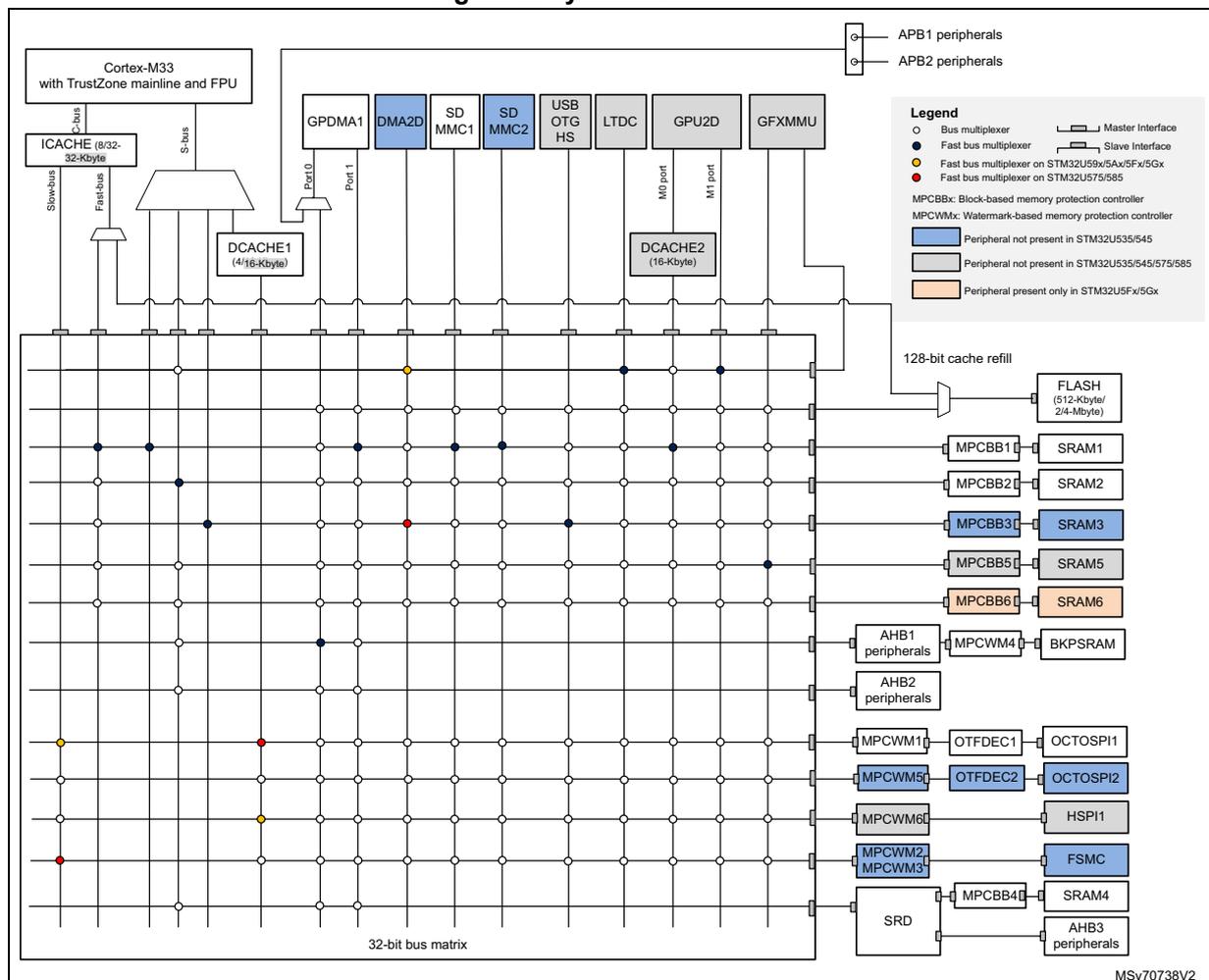
The diagram illustrates the system architecture of the STM32U5 series microcontroller. At the top, the Cortex-M33 core with TrustZone mainline and FPU is connected to the bus matrix via its C-bus and S-bus. The C-bus connects through the ICACHE (8/32-32-Kbyte) and the Slowbus to the matrix. The S-bus connects through the DCACHE1 (4/16-Kbyte) and the Fastbus to the matrix. The matrix itself is a 32-bit wide grid. Various masters are connected to the matrix: GPDMA1, DMA2D, SD MMC1, SD MMC2, USB OTG HS, LTDC, GPU2D, and GFXMMU. The matrix also connects to various slave components: FLASH (512-Kbyte/2/4-Mbyte), SRAM1, SRAM2, SRAM3, SRAM5, SRAM6, BKPSRAM, OCTOSPI1, OCTOSPI2, HSPI1, FSMC, SRAM4, and AHB3 peripherals. A legend on the right side defines the symbols used for different types of bus multiplexers and memory protection controllers. The diagram also indicates the presence of APB1 and APB2 peripherals, and the availability of certain peripherals based on the specific microcontroller model (e.g., STM32U535/545, STM32U575/585, or STM32U5F5/5Gx).
2.1.1 Fast C-bus
This bus connects the C-bus of the Cortex-M33 core to the internal flash memory and to the bus matrix via the instruction cache. This bus is used for instruction fetch and data access to the internal memories mapped in the code region. This bus targets the internal flash memory and the internal SRAMs (SRAM1, SRAM2, SRAM3, SRAM5, and SRAM6).
SRAM1, SRAM2, SRAM3, SRAM5, and SRAM6 are accessible on this bus with a continuous mapping.
2.1.2 Slow C-bus
This bus connects the C-bus of the Cortex-M33 core to the bus matrix via the instruction cache. This bus is used for instruction fetch and data access to the external memories mapped in the code region. This bus targets the external memories (FSMC, HSPI1, and OCTOSPIs).
2.1.3 S-bus
This bus connects the system bus of the Cortex-M33 core to the bus matrix. This bus is used by the core to access data located in a peripheral or SRAM area. This bus targets the internal SRAMs (SRAM1, SRAM2, SRAM3, SRAM4, SRAM5, SRAM6, and BKPSRAM), the AHB1 peripherals including the APB1 and APB2 peripherals, the AHB2 peripherals and the SRD peripherals.
SRAM1, SRAM2, SRAM3, SRAM5, and SRAM6 are accessible on this bus with a continuous mapping.
Note: The bus matrix has a zero latency when accessing SRAM1, SRAM2, SRAM3, SRAM5, and SRAM6.
2.1.4 DCACHE S-bus
This bus connects the system bus of the Cortex-M33 core to the bus matrix via the data cache. This bus is used for instruction fetch and data access to the external memories mapped in the data region. This bus targets the external memories (FSMC, HSPI1, GFXMMU, and OCTOSPIs).
Note: Fetching instructions through this bus is less efficient than fetching instructions through the slow C-bus.
2.1.5 GPDMA-bus
These buses connect the two AHB master interfaces of the GPDMA to the bus matrix. These buses target the internal flash memory, the internal SRAMs (SRAM1, SRAM2, SRAM3, SRAM4, SRAM5, SRAM6, and BKPSRAM), the AHB1 peripherals including the APB1 and APB2 peripherals, the AHB2 peripherals, the SRD peripherals and the external memories through FSMC, HSPI1, or OCTOSPIs.
2.1.6 OTG_HS-bus
This bus connects the OTG_HS master interface to the bus matrix. This bus is used only by the OTG_HS to load/store data from/to the memory. This bus targets the data memories: internal flash memory, internal SRAMs (SRAM1, SRAM2, SRAM3, SRAM5, and SRAM6) and external memories through FSMC, HSPI1, or OCTOSPIs.
2.1.7 LTDC-bus
This bus connects the LTDC master interface to the bus matrix. This bus is used only to load data from the memory. This bus targets the GFXMMU in addition to the data memories: internal flash memory, internal SRAMs (SRAM1, SRAM2, SRAM3, SRAM5, and SRAM6) and external memories through FSMC, HSPI1 or OCTOSPIs.
2.1.8 GPU2D-bus
These buses connect the GPU2D master interfaces to the bus matrix. These buses are used only by the GPU2D to load/store data from/to the memory. These buses target the GFXMMU in addition to the data memories: internal flash memory, internal SRAMs (SRAM1, SRAM2, SRAM3, SRAM5, and SRAM6) and external memories through FSMC, HSPI1, or OCTOSPIs. A 16-Kbyte data cache (DCACHE2) is present on the GPU2D M0 bus in order to improve performances.
2.1.9 GFXMMU-bus
This bus connects the GFXMMU master interface to the bus matrix. This bus is used only by the GFXMMU to load/store data from/to the memory. This bus targets the data memories: internal flash memory, internal SRAMs (SRAM1, SRAM2, SRAM3, SRAM5, and SRAM6) and external memories through FSMC, HSPI1, or OCTOSPIs. The GFXMMU has also a slave bus connection to be accessed by graphical peripheral master buses.
2.1.10 SDMMC1 and SDMMC2 controllers DMA buses
These buses connect the SDMMC1 and SDMMC2 DMA master interfaces to the bus matrix. These buses are used only by the SDMMC1 and SDMMC2 DMA to load/store data from/to the memory. These buses target the data memories: internal flash memory, internal SRAMs (SRAM1, SRAM2, SRAM3, SRAM5, and SRAM6) and external memories through FSMC, HSPI1, or OCTOSPIs.
2.1.11 Bus matrix
The bus matrix manages the access arbitration between masters. The arbitration uses a round-robin algorithm. This bus matrix features a fast bus multiplexer used to connect each master to a given slave without latency (see Figure 1 ). For the same master, other slaves undergo a latency of at least one cycle at each new access.
2.1.12 AHB/APB bridges
The three AHB/APB bridges provide full synchronous connections between the AHB and the APB buses, allowing flexible selection of the peripheral frequency.
Refer to Section 2.3.2: Memory map and register boundary addresses for the address mapping of the peripherals connected to these bridges.
After each device reset, all peripheral clocks are disabled (except for the internal SRAMs and flash memory interfaces). Before using a peripheral, its clock must be enabled in the RCC_AHBxENR and RCC_APBxENR registers.
Note: When an 8- or 16-bit access is performed on an APB register, the access is transformed into a 32-bit access: the bridge duplicates the 8- or 16-bit data to feed the 32-bit vector.
2.1.13 SmartRun domain (SRD)
The SRD architecture relies on a DMA allowing autonomous operation during low-power modes down to Stop 2.
This architecture also features a 32-bit AHB bus matrix that interconnects:
- • two masters:
- – the main AHB bus matrix
- – LPDMA1 (low-power DMA featuring one master port)
- • two slaves:
- – AHB3 peripherals including AHB to APB bridge connected to APB3
- – internal SRAM4
Note: The SRAM4 is the only SRAM that can be accessed by the LPDMA1.
This architecture is shown in the figure below.
Figure 2. SmartRun domain architecture
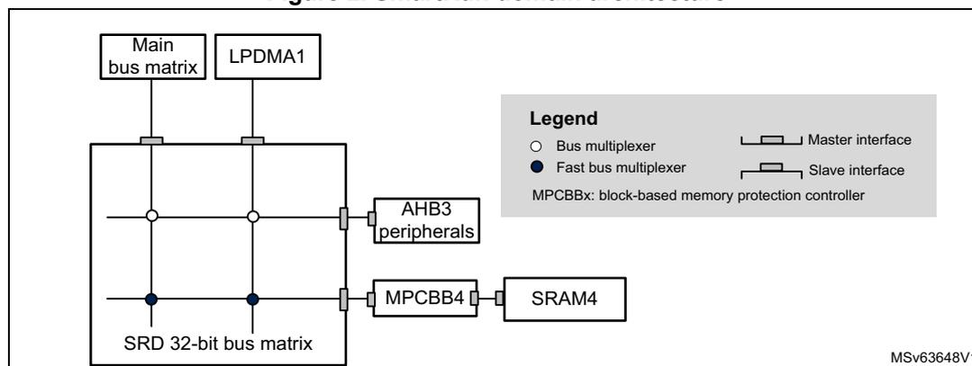
The diagram illustrates the SmartRun domain architecture. At the top, the 'Main bus matrix' and 'LPDMA1' are connected to a central 'SRD 32-bit bus matrix'. The 'SRD 32-bit bus matrix' is connected to 'AHB3 peripherals' and 'MPCBB4'. 'MPCBB4' is connected to 'SRAM4'. A legend on the right defines the symbols: a white circle for 'Bus multiplexer', a black circle for 'Fast bus multiplexer', a rectangle with a small circle for 'Master interface', a rectangle with a small rectangle for 'Slave interface', and 'MPCBBx: block-based memory protection controller'. The reference 'MSv63648V1' is shown in the bottom right corner.
2.2 Arm TrustZone security architecture
The security architecture is based on Arm TrustZone with the Armv8-M mainline extension.
The TrustZone security is activated by the TZEN option bit in the FLASH_OPTR register.
When the TrustZone is enabled, the SAU (security-attribution unit) and IDAU (implementation-defined-attribution unit) define the access permissions based on secure and nonsecure states.
- • SAU: Up to eight SAU configurable regions are available for security attribution.
- • IDAU: provides a first memory partition as nonsecure or nonsecure callable attributes. The IDAU memory map partition is not configurable and fixed by hardware implementation (refer to Figure 3 to Figure 6 in Section 2.3.2: Memory map and register boundary addresses ). It is then combined with the results from the SAU security attribution and the higher security state is selected.
Based on IDAU security attribution, the flash memory, system SRAMs, and peripherals memory space are aliased twice for secure and nonsecure states. The external memories space is not aliased.
The table below shows an example of typical eight SAU regions mapping based on IDAU regions. The user can split and choose the secure, nonsecure or NSC regions for external memories as needed.
Table 3. Example of memory map security attribution versus SAU configuration regions
| Region description | Address range | IDAU security attribution | SAU security attribution typical configuration | Final security attribution |
|---|---|---|---|---|
| Code - external memories | 0x0000_0000 0x07FF_FFFF | Nonsecure | Secure, nonsecure or NSC (1) | Secure, nonsecure, or NSC |
| Code - flash memory and SRAM | 0x0800_0000 0x0BFF_FFFF | Nonsecure | Nonsecure | Nonsecure |
| 0x0C00_0000 0x0FFF_FFFF | NSC | Secure or NSC | Secure or NSC |
Table 3. Example of memory map security attribution versus SAU configuration regions
| Region description | Address range | IDAU security attribution | SAU security attribution typical configuration | Final security attribution |
|---|---|---|---|---|
| Code - external memories | 0x1000_0000 0x17FF_FFFF | Nonsecure | Nonsecure | |
| 0x1800_0000 0x1FFF_FFFF | ||||
| SRAM | 0x2000_0000 0x2FFF_FFFF | Nonsecure | ||
| 0x3000_0000 0x3FFF_FFFF | NSC | Secure or NSC | Secure or NSC | |
| Peripherals | 0x4000_0000 0x4FFF_FFFF | Nonsecure | Nonsecure | Nonsecure |
| 0x5000_0000 0x5FFF_FFFF | NSC | Secure or NSC | Secure or NSC | |
| External memories | 0x6000_0000 0xDFFF_FFFF | Nonsecure | Secure, nonsecure or NSC | Secure, nonsecure or NSC |
1. NSC = nonsecure callable
2.2.1 Default Arm TrustZone security state
When the TrustZone security is activated by the TZEN option bit in the FLASH_OPTR, the default system security state is detailed below:
- • CPU:
- – Cortex-M33 is in secure state after reset. The boot address must be at a secure address.
- • memory map:
- – SAU is fully secure after reset. Consequently, all memory map is fully secure. Up to height SAU configurable regions are available for security attribution.
- • flash memory:
- – The flash memory security area is defined by watermark user options.
- – Flash block-based security attributions are nonsecure after reset.
- • SRAMs:
- – All SRAMs are secure after reset. MPCBBx (block-based memory protection controller) are secure.
- • external memories:
- – FSMC, HSPI1 and OCTOSPIs banks are secure after reset. MPCWMx (watermark-based memory protection controller) are secure.
- • peripherals (see
Table 4
and
Table 5
for a list of securable and TrustZone-aware peripherals)
- – Securables peripherals are nonsecure after reset.
- – TrustZone-aware peripherals are nonsecure after reset. Their secure configuration registers are secure.
- • all GPIOs secure after reset
- • interrupts:
- – NVIC: All interrupts are secure after reset. NVIC is banked for secure and nonsecure state.
- – TZIC: All illegal access interrupts are disabled after reset (see GTZC TrustZone system architecture ).
2.2.2 Arm TrustZone peripheral classification
When the TrustZone security is active, a peripheral can be either securable or TrustZone-aware type as follows:
- • Securable: peripheral protected by an AHB/APB firewall gate that is controlled from TZSC controller to define security properties
- • TrustZone-aware: peripheral connected directly to AHB or APB bus and implementing a specific TrustZone behavior such as a subset of registers being secure.
Refer to GTZC TrustZone system architecture for more details.
The tables below list the securable and TrustZone-aware peripherals within the system.
Table 4. Securable peripherals by TZSC
| Bus | Peripheral | STM32U535/545 | STM32U575/585 | STM32U59x/5Ax | STM32U5Fx/5Gx |
|---|---|---|---|---|---|
| AHB3 | ADF1 | X | X | X | X |
| DAC1 | X | X | X | X | |
| ADC4 | X | X | X | X | |
| AHB2 | OCTOSPI2 registers | - | X | X | X |
| OCTOSPI1 registers | X | X | X | X | |
| HSPI1 registers | - | - | X | X | |
| FSMC registers | - | X | X | X | |
| SDMMC1 | X | X | X | X | |
| SDMMC2 | - | X | X | X | |
| OCTOSPIM | - | X | X | X | |
| SAES | X | X | X | X | |
| PKA | X | X | X | X | |
| RNG | X | X | X | X | |
| HASH | X | X | X | X | |
| AES | X | X | X | X | |
| USB | X | - | - | - | |
| OTG_FS | - | X | - | - | |
| OTG_HS | - | - | X | X | |
| DCMI | X | X | X | X | |
| ADC12 | X | X | X | X |
Table 4. Securable peripherals by TZSC (continued)
| Bus | Peripheral | STM32U535/545 | STM32U575/585 | STM32U59x/5Ax | STM32U5Fx/5Gx |
|---|---|---|---|---|---|
| AHB1 | GFXMMU registers | - | - | X | X |
| GPU2D registers | - | - | X | X | |
| JPEG | - | - | - | X | |
| DCACHE2 registers | - | - | X | X | |
| DCACHE1 registers (1) | X | X | X | X | |
| ICACHE registers (1) | X | X | X | X | |
| DMA2D | - | X | X | X | |
| TSC | X | X | X | X | |
| CRC | X | X | X | X | |
| RAMCFG | X | X | X | X | |
| MDF1 | X | X | X | X | |
| FMAC | X | X | X | X | |
| CORDIC | X | X | X | X | |
| APB3 | VREFBUF | X | X | X | X |
| COMP (2) | X | X | X | X | |
| OPAMP | X | X | X | X | |
| LPTIM4 | X | X | X | X | |
| LPTIM3 | X | X | X | X | |
| LPTIM1 | X | X | X | X | |
| I2C3 | X | X | X | X | |
| LPUART1 | X | X | X | X | |
| SPI3 | X | X | X | X | |
| APB2 | DSI | - | - | X | X |
| LTDC | - | - | X | X | |
| GFXTIM | - | - | - | X | |
| SAI2 | - | X | X | X | |
| SAI1 | X | X | X | X | |
| TIM17 | X | X | X | X | |
| TIM16 | X | X | X | X | |
| TIM15 | X | X | X | X | |
| USART1 | X | X | X | X | |
| TIM8 | X | X | X | X | |
| SPI1 | X | X | X | X | |
| TIM1 | X | X | X | X |
Table 4. Securable peripherals by TZSC (continued)
| Bus | Peripheral | STM32U535/545 | STM32U575/585 | STM32U59x/5Ax | STM32U5Fx/5Gx |
|---|---|---|---|---|---|
| APB1 | I2C6 | - | - | X | X |
| I2C5 | - | - | X | X | |
| USART6 | - | - | X | X | |
| UCPD1 | - | X | X | X | |
| FDCAN1 | X | X | X | X (3) | |
| LPTIM2 | X | X | X | X | |
| I2C4 | X | X | X | X | |
| CRS | X | X | X | X | |
| I2C2 | X | X | X | X | |
| I2C1 | X | X | X | X | |
| UART5 | X | X | X | X | |
| UART4 | X | X | X | X | |
| USART3 | X | X | X | X | |
| USART2 | - | X | X | X | |
| SPI2 | X | X | X | X | |
| IWDG | X | X | X | X | |
| WWDG | X | X | X | X | |
| TIM7 | X | X | X | X | |
| TIM6 | X | X | X | X | |
| TIM5 | X | X | X | X | |
| TIM4 | X | X | X | X | |
| TIM3 | X | X | X | X | |
| TIM2 | X | X | X | X |
1. ICACHE and DCACHE1 are TrustZone-aware peripherals, regardless if access to their registers is secured by TZSC.
2. Only one COMP on STM32U535/545.
3. FDCAN1 is not present on STM32U5Fx devices.
Table 5. TrustZone aware peripherals
| Bus | Peripheral | STM32U535/545 | STM32U575/585 | STM32U59x/5Ax | STM32U5Fx/5Gx |
|---|---|---|---|---|---|
| AHB3 | GTZC2 | X | X | X | X |
| EXTI | X | X | X | X | |
| LPDMA1 | X | X | X | X | |
| RCC | X | X | X | X | |
| PWR | X | X | X | X | |
| LPGPIO1 | X | X | X | X |
Table 5. TrustZone aware peripherals (continued)
| Bus | Peripheral | STM32U535/545 | STM32U575/585 | STM32U59x/5Ax | STM32U5Fx/5Gx |
|---|---|---|---|---|---|
| AHB2 | OTFDEC1 (1) | X | X | X | X |
| OTFDEC2 (1) | - | X | X | X | |
| GPIOJ | - | - | X | X | |
| GPIOI | - | X | X | X | |
| GPIOH | X | X | X | X | |
| GPIOG | X | X | X | X | |
| GPIOF | - | X | X | X | |
| GPIOE | X | X | X | X | |
| GPIO D | X | X | X | X | |
| GPIOC | X | X | X | X | |
| GPIOB | X | X | X | X | |
| GPIOA | X | X | X | X | |
| AHB1 | GTZC1 | X | X | X | X |
| FLASH | X | X | X | X | |
| GPDMA1 | X | X | X | X | |
| APB3 | TAMP | X | X | X | X |
| RTC | X | X | X | X | |
| SYSCFG | X | X | X | X |
1. Always secure when TZEN = 1.
2.3 Memory organization
2.3.1 Introduction
Program memory, data memory, registers and I/O ports are organized within the same linear 4-Gbyte address space.
The bytes are coded in memory in Little Endian format. The lowest numbered byte in a word is considered the word's least significant byte and the highest numbered byte the most significant.
2.3.2 Memory map and register boundary addresses
Figure 3. Memory map based on IDAU mapping for STM32U535/545
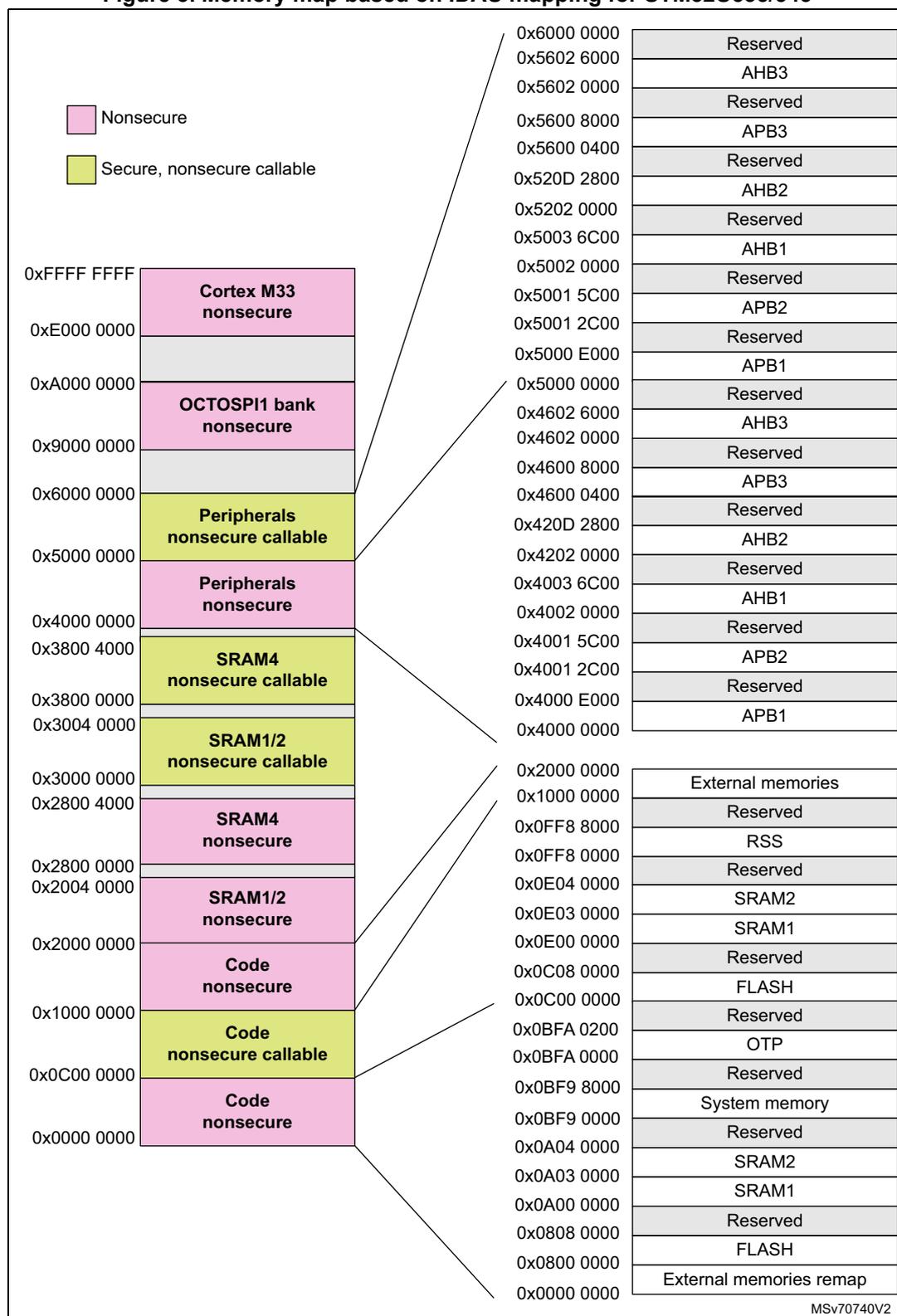
Legend:
- Nonsecure (Pink)
- Secure, nonsecure callable (Green)
Memory Map:
| Address Range | Memory Region | Security Status |
|---|---|---|
| 0xFFFF FFFF to 0xE000 0000 | Cortex M33 | Nonsecure |
| 0xA000 0000 to 0x9000 0000 | OCTOSPI1 bank | Nonsecure |
| 0x6000 0000 to 0x5000 0000 | Peripherals | Secure, nonsecure callable |
| 0x5000 0000 to 0x4000 0000 | Peripherals | Nonsecure |
| 0x3800 4000 to 0x3800 0000 | SRAM4 | Secure, nonsecure callable |
| 0x3004 0000 to 0x3000 0000 | SRAM1/2 | Secure, nonsecure callable |
| 0x2800 4000 to 0x2800 0000 | SRAM4 | Nonsecure |
| 0x2004 0000 to 0x2000 0000 | SRAM1/2 | Nonsecure |
| 0x1000 0000 to 0x0C00 0000 | Code | Nonsecure |
| 0x0C00 0000 to 0x0000 0000 | Code | Secure, nonsecure callable |
Register Boundary Addresses:
| Address Range | Register Name |
|---|---|
| 0x6000 0000 to 0x5602 6000 | Reserved |
| 0x5602 6000 to 0x5602 0000 | AHB3 |
| 0x5602 0000 to 0x5600 8000 | Reserved |
| 0x5600 8000 to 0x5600 0400 | APB3 |
| 0x5600 0400 to 0x520D 2800 | Reserved |
| 0x520D 2800 to 0x5202 0000 | AHB2 |
| 0x5202 0000 to 0x5003 6C00 | Reserved |
| 0x5003 6C00 to 0x5002 0000 | AHB1 |
| 0x5002 0000 to 0x5001 5C00 | Reserved |
| 0x5001 5C00 to 0x5001 2C00 | APB2 |
| 0x5001 2C00 to 0x5000 E000 | Reserved |
| 0x5000 E000 to 0x5000 0000 | APB1 |
| 0x5000 0000 to 0x4602 6000 | Reserved |
| 0x4602 6000 to 0x4602 0000 | AHB3 |
| 0x4602 0000 to 0x4600 8000 | Reserved |
| 0x4600 8000 to 0x4600 0400 | APB3 |
| 0x4600 0400 to 0x420D 2800 | Reserved |
| 0x420D 2800 to 0x4202 0000 | AHB2 |
| 0x4202 0000 to 0x4003 6C00 | Reserved |
| 0x4003 6C00 to 0x4002 0000 | AHB1 |
| 0x4002 0000 to 0x4001 5C00 | Reserved |
| 0x4001 5C00 to 0x4001 2C00 | APB2 |
| 0x4001 2C00 to 0x4000 E000 | Reserved |
| 0x4000 E000 to 0x4000 0000 | APB1 |
| 0x2000 0000 to 0x1000 0000 | External memories |
| 0x1000 0000 to 0x0FF8 8000 | Reserved |
| 0x0FF8 8000 to 0x0FF8 0000 | RSS |
| 0x0FF8 0000 to 0x0E04 0000 | Reserved |
| 0x0E04 0000 to 0x0E03 0000 | SRAM2 |
| 0x0E03 0000 to 0x0E00 0000 | SRAM1 |
| 0x0E00 0000 to 0x0C08 0000 | Reserved |
| 0x0C08 0000 to 0x0C00 0000 | FLASH |
| 0x0C00 0000 to 0x0BFA 0200 | Reserved |
| 0x0BFA 0200 to 0x0BFA 0000 | OTP |
| 0x0BFA 0000 to 0x0BF9 8000 | Reserved |
| 0x0BF9 8000 to 0x0BF9 0000 | System memory |
| 0x0BF9 0000 to 0x0A04 0000 | Reserved |
| 0x0A04 0000 to 0x0A03 0000 | SRAM2 |
| 0x0A03 0000 to 0x0A00 0000 | SRAM1 |
| 0x0A00 0000 to 0x0808 0000 | Reserved |
| 0x0808 0000 to 0x0800 0000 | FLASH |
| 0x0800 0000 to 0x0000 0000 | External memories remap |
MSv70740V2
Figure 4. Memory map based on IDAU mapping for STM32U575/585
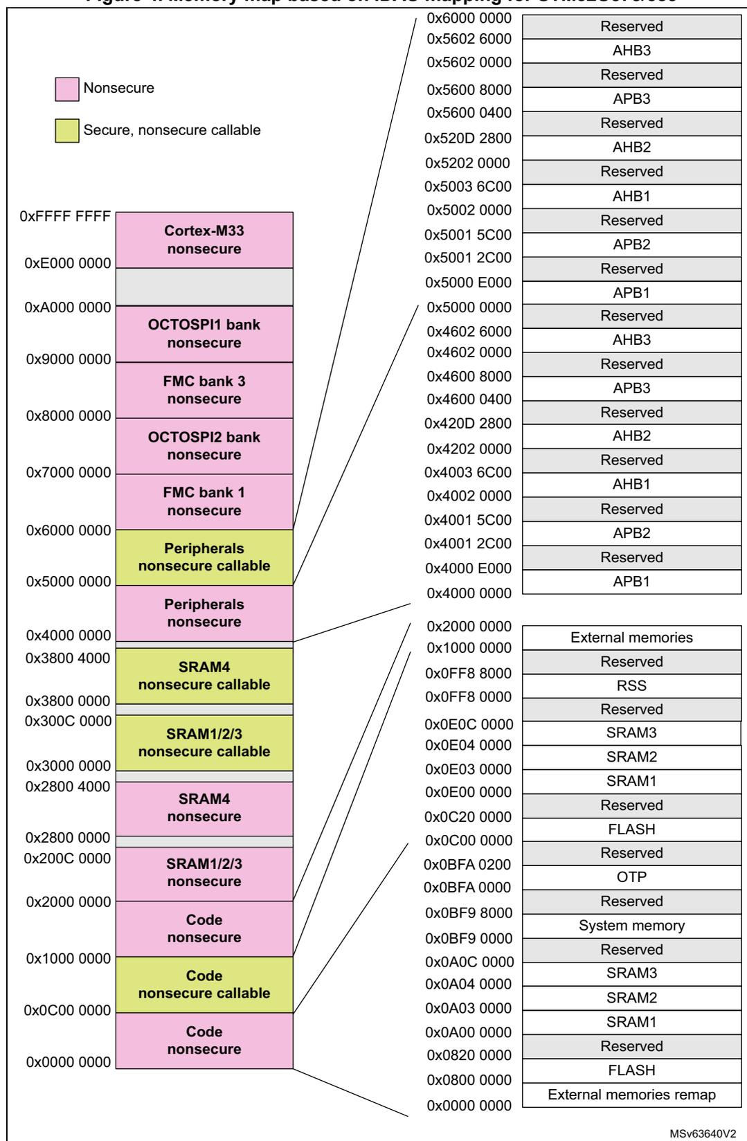
Legend:
- Nonsecure (Pink)
- Secure, nonsecure callable (Green)
| Address Range | Memory Type |
|---|---|
| 0x0000 0000 - 0x0000 0000 | External memories remap |
| 0x0800 0000 - 0x0820 0000 | FLASH |
| 0x0A00 0000 - 0x0A03 0000 | SRAM1 |
| 0x0A04 0000 - 0x0A0C 0000 | SRAM2 |
| 0x0BF9 0000 - 0x0BF9 8000 | System memory |
| 0x0BFA 0000 - 0x0BFA 0200 | OTP |
| 0x0C00 0000 - 0x0C20 0000 | FLASH |
| 0x0E00 0000 - 0x0E03 0000 | SRAM1 |
| 0x0E04 0000 - 0x0E0C 0000 | SRAM2 |
| 0x0FF8 0000 - 0x0FF8 8000 | RSS |
| 0x1000 0000 - 0x2000 0000 | External memories |
| 0x4000 0000 - 0x4000 0000 | APB1 |
| 0x4001 2C00 - 0x4001 5C00 | Reserved |
| 0x4002 0000 - 0x4002 2C00 | APB2 |
| 0x4003 6C00 - 0x4003 8000 | Reserved |
| 0x4202 0000 - 0x4202 2800 | AHB1 |
| 0x4600 0000 - 0x4600 0400 | Reserved |
| 0x4602 0000 - 0x4602 6000 | APB3 |
| 0x5000 0000 - 0x5000 E000 | Reserved |
| 0x5001 2C00 - 0x5001 5C00 | APB1 |
| 0x5202 0000 - 0x5202 2800 | Reserved |
| 0x5600 0000 - 0x5600 0400 | AHB2 |
| 0x5602 0000 - 0x5602 6000 | Reserved |
| 0x6000 0000 - 0x6000 0000 | Reserved |
Main Memory Map:
| Address Range | Memory Type |
|---|---|
| 0x0000 0000 - 0x0C00 0000 | Code nonsecure |
| 0x0C00 0000 - 0x1000 0000 | Code nonsecure callable |
| 0x1000 0000 - 0x2000 0000 | Code nonsecure |
| 0x2000 0000 - 0x2800 0000 | SRAM1/2/3 nonsecure |
| 0x2800 0000 - 0x3000 0000 | SRAM4 nonsecure |
| 0x3000 0000 - 0x3800 0000 | SRAM1/2/3 nonsecure callable |
| 0x3800 0000 - 0x4000 0000 | SRAM4 nonsecure callable |
| 0x4000 0000 - 0x5000 0000 | Peripherals nonsecure |
| 0x5000 0000 - 0x6000 0000 | Peripherals nonsecure callable |
| 0x6000 0000 - 0x7000 0000 | FMC bank 1 nonsecure |
| 0x7000 0000 - 0x8000 0000 | OCTOSPI2 bank nonsecure |
| 0x8000 0000 - 0x9000 0000 | FMC bank 3 nonsecure |
| 0x9000 0000 - 0xA000 0000 | OCTOSPI1 bank nonsecure |
| 0xA000 0000 - 0xE000 0000 | (Reserved) |
| 0xE000 0000 - 0xFFFF FFFF | Cortex-M33 nonsecure |
MSv63640V2
Figure 5. Memory map based on IDAU mapping for STM32U59x/5Ax
Legend:
- Nonsecure (Pink)
- Secure, nonsecure callable (Green)
| Address Range | Memory Type |
|---|---|
| 0x0000 0000 - 0x1000 0000 | Code nonsecure |
| 0x1000 0000 - 0x2000 0000 | Code nonsecure callable |
| 0x2000 0000 - 0x2400 0000 | Code nonsecure |
| 0x2400 0000 - 0x2500 0000 | GFXMMU virtual buffer nonsecure |
| 0x2500 0000 - 0x2800 0000 | SRAM1/2/3/5 nonsecure |
| 0x2800 0000 - 0x3000 0000 | SRAM4 nonsecure |
| 0x3000 0000 - 0x3400 0000 | SRAM1/2/3/5 nonsecure callable |
| 0x3400 0000 - 0x3500 0000 | GFXMMU virtual buffer nonsecure callable |
| 0x3500 0000 - 0x3800 0000 | SRAM4 nonsecure callable |
| 0x3800 0000 - 0x4000 0000 | Peripherals nonsecure |
| 0x4000 0000 - 0x5000 0000 | Peripherals nonsecure callable |
| 0x5000 0000 - 0x6000 0000 | FMC bank 1 nonsecure |
| 0x6000 0000 - 0x7000 0000 | OCTOSPI2 bank nonsecure |
| 0x7000 0000 - 0x8000 0000 | FMC bank 3 nonsecure |
| 0x8000 0000 - 0x9000 0000 | OCTOSPI1 bank nonsecure |
| 0x9000 0000 - 0xA000 0000 | HSPI1 bank nonsecure |
| 0xA000 0000 - 0xE000 0000 | Cortex M33 nonsecure |
| 0xE000 0000 - 0xFFFF FFFF | Reserved |
| Address Range | Memory Type |
|---|---|
| 0x0000 0000 - 0x0800 0000 | External memories remap |
| 0x0800 0000 - 0x0840 0000 | Reserved |
| 0x0840 0000 - 0x0A00 0000 | FLASH |
| 0x0A00 0000 - 0x0A0C 0000 | SRAM1 |
| 0x0A0C 0000 - 0x0A0D 0000 | SRAM2 |
| 0x0A0D 0000 - 0x0A1A 0000 | SRAM3 |
| 0x0A1A 0000 - 0x0A27 0000 | SRAM5 |
| 0x0A27 0000 - 0x0BF9 0000 | Reserved |
| 0x0BF9 0000 - 0x0BF9 8000 | System memory |
| 0x0BF9 8000 - 0x0BFA 0000 | Reserved |
| 0x0BFA 0000 - 0x0BFA 0200 | OTP |
| 0x0BFA 0200 - 0x0C00 0000 | Reserved |
| 0x0C00 0000 - 0x0C40 0000 (3) | FLASH |
| 0x0C40 0000 (3) - 0x0E00 0000 | Reserved |
| 0x0E00 0000 - 0x0E0C 0000 | SRAM1 |
| 0x0E0C 0000 - 0x0E0D 0000 | SRAM2 |
| 0x0E0D 0000 - 0x0E1A 0000 | SRAM3 |
| 0x0E1A 0000 - 0x0E27 0000 | SRAM5 |
| 0x0E27 0000 - 0x0FF8 0000 | Reserved |
| 0x0FF8 0000 - 0x0FF8 8000 | RSS |
| 0x0FF8 8000 - 0x1000 0000 | Reserved |
| 0x1000 0000 - 0x2000 0000 | External memories |
| Address Range | Memory Type |
|---|---|
| 0x4000 0000 - 0x4000 0000 | APB1 |
| 0x4000 E000 - 0x4001 2C00 | Reserved |
| 0x4001 2C00 - 0x4001 7C00 | APB2 |
| 0x4001 7C00 - 0x4002 0000 | Reserved |
| 0x4002 0000 - 0x4003 6C00 | AHB1 |
| 0x4003 6C00 - 0x4202 0000 | Reserved |
| 0x4202 0000 - 0x420D 3800 | AHB2 |
| 0x420D 3800 - 0x4600 0400 | Reserved |
| 0x4600 0400 - 0x4600 8000 | APB3 |
| 0x4600 8000 - 0x4602 0000 | Reserved |
| 0x4602 0000 - 0x4602 6000 | AHB3 |
| 0x4602 6000 - 0x5000 0000 | Reserved |
| 0x5000 0000 - 0x5000 E000 | APB1 |
| 0x5000 E000 - 0x5001 2C00 | Reserved |
| 0x5001 2C00 - 0x5001 7C00 | APB2 |
| 0x5001 7C00 - 0x5002 0000 | Reserved |
| 0x5002 0000 - 0x5003 6C00 | AHB1 |
| 0x5003 6C00 - 0x5202 0000 | Reserved |
| 0x5202 0000 - 0x520D 3800 | AHB2 |
| 0x520D 3800 - 0x5600 0400 | Reserved |
| 0x5600 0400 - 0x5600 8000 | APB3 |
| 0x5600 8000 - 0x5602 0000 | Reserved |
| 0x5602 0000 - 0x5602 6000 | AHB3 |
| 0x5602 6000 - 0x6000 0000 | Reserved |
MSv65678V2
Figure 6. Memory map based on IDAU mapping for STM32U5Fx/5Gx
Legend:
- Nonsecure (Pink)
- Secure, nonsecure callable (Green)
| Address Range | Memory Type | Address Range | Memory Type |
|---|---|---|---|
| 0x0000 0000 - 0x1000 0000 | Code nonsecure | 0x0000 0000 - 0x0800 0000 | External memories remap |
| 0x1000 0000 - 0x2000 0000 | Code nonsecure callable | 0x0800 0000 - 0x0840 0000 | FLASH |
| 0x2000 0000 - 0x2400 0000 | Code nonsecure | 0x0840 0000 - 0x0A00 0000 | Reserved |
| 0x2400 0000 - 0x2500 0000 | GFXMMU virtual buffer nonsecure | 0x0A00 0000 - 0x0A0C 0000 | SRAM1 |
| 0x2500 0000 - 0x2800 0000 | SRAM4 nonsecure | 0x0A0C 0000 - 0x0A0D 0000 | SRAM2 |
| 0x2800 0000 - 0x3000 0000 | SRAM1/2/3/5/6 nonsecure | 0x0A0D 0000 - 0x0A1A 0000 | SRAM3 |
| 0x3000 0000 - 0x3400 0000 | SRAM1/2/3/5/6 nonsecure | 0x0A1A 0000 - 0x0A27 0000 | SRAM5 |
| 0x3400 0000 - 0x3500 0000 | GFXMMU virtual buffer nonsecure | 0x0A27 0000 - 0x0A2F 0000 | SRAM6 |
| 0x3500 0000 - 0x3800 0000 | SRAM4 nonsecure | 0x0A2F 0000 - 0x0BF9 0000 | Reserved |
| 0x3800 0000 - 0x4000 0000 | SRAM4 nonsecure | 0x0BF9 0000 - 0x0BFA 0000 | System memory |
| 0x4000 0000 - 0x5000 0000 | Peripherals nonsecure | 0x0BFA 0000 - 0x0BFA 0200 | Reserved |
| 0x5000 0000 - 0x6000 0000 | Peripherals nonsecure callable | 0x0BFA 0200 - 0x0C00 0000 | OTP |
| 0x6000 0000 - 0x7000 0000 | FMC bank 1 nonsecure | 0x0C00 0000 - 0x0C40 0000 | FLASH |
| 0x7000 0000 - 0x8000 0000 | OCTOSPI2 bank nonsecure | 0x0C40 0000 - 0x0E00 0000 | Reserved |
| 0x8000 0000 - 0x9000 0000 | FMC bank 3 nonsecure | 0x0E00 0000 - 0x0E0C 0000 | SRAM1 |
| 0x9000 0000 - 0xA000 0000 | OCTOSPI1 bank nonsecure | 0x0E0C 0000 - 0x0E0D 0000 | SRAM2 |
| 0xA000 0000 - 0xB000 0000 | HSPI1 bank nonsecure | 0x0E0D 0000 - 0x0E1A 0000 | SRAM3 |
| 0xB000 0000 - 0xE000 0000 | Reserved | 0x0E1A 0000 - 0x0E27 0000 | SRAM5 |
| 0xE000 0000 - 0xFFFF FFFF | Cortex M33 nonsecure | 0x0E27 0000 - 0x0E2F 0000 | SRAM6 |
| 0x0E2F 0000 - 0x0FF8 0000 | Reserved | ||
| 0x0FF8 0000 - 0x0FF8 8000 | RSS | ||
| 0x0FF8 8000 - 0x1000 0000 | Reserved | ||
| 0x1000 0000 - 0x2000 0000 | External memories |
Additional Address Ranges:
- 0x5000 0000 - 0x5001 2C00: APB2
- 0x5001 2C00 - 0x5001 7C00: Reserved
- 0x5001 7C00 - 0x5002 0000: APB1
- 0x5002 0000 - 0x5202 0000: Reserved
- 0x5202 0000 - 0x520D 3800: AHB2
- 0x520D 3800 - 0x5600 0400: Reserved
- 0x5600 0400 - 0x5600 8000: APB3
- 0x5600 8000 - 0x5602 0000: Reserved
- 0x5602 0000 - 0x5602 6000: AHB3
- 0x5602 6000 - 0x6000 0000: Reserved
MSv70739V2
All memory-map areas that are not allocated to on-chip memories and peripherals are considered “Reserved”. The table below gives the boundary addresses of the peripherals available in the devices.
Table 6. Memory map and peripheral register boundary addresses
| Bus | Secure boundary address | Nonsecure boundary address | Size (bytes) | Peripheral | Peripheral register map | STM32U535/545 | STM32U575/585 | STM32U59x/5Ax | STM32U5Fx/5Gx |
|---|---|---|---|---|---|---|---|---|---|
| AHB3 | 0x5602 6000 - 0x5FFF FFFF | 0x4602 6000 - 0x4FFF FFFF | 164 M | Reserved | - | - | - | - | - |
| 0x5602 5000 - 0x5602 5FFF | 0x4602 5000 - 0x4602 5FFF | 4 K | LPDMA1 | LPDMA register map | X | X | X | X | |
| 0x5602 4000 - 0x5602 4FFF | 0x4602 4000 - 0x4602 4FFF | 4 K | ADF1 | ADF register map | X | X | X | X | |
| 0x5602 3C00 - 0x5602 3FFF | 0x4602 3C00 - 0x4602 3FFF | 1 K | Reserved | - | - | - | - | - | |
| 0x5602 3800 - 0x5602 3BFF | 0x4602 3800 - 0x4602 3BFF | 1 K | GTZC2_MPCBB4 | GTZC2 MPCBB4 register map | X | X | X | X | |
| 0x5602 3400 - 0x5602 37FF | 0x4602 3400 - 0x4602 37FF | 1 K | GTZC2_TZIC | GTZC2 TZIC register map | X | X | X | X | |
| 0x5602 3000 - 0x5602 33FF | 0x4602 3000 - 0x4602 33FF | 1 K | GTZC2_TZSC | GTZC2 TZSC register map | X | X | X | X | |
| 0x5602 2400 - 0x5602 2FFF | 0x4602 2400 - 0x4602 2FFF | 3 K | Reserved | - | - | - | - | - | |
| 0x5602 2000 - 0x5602 23FF | 0x4602 2000 - 0x4602 23FF | 1 K | EXTI | EXTI register map | X | X | X | X | |
| 0x5602 1C00 - 0x5602 1FFF | 0x4602 1C00 - 0x4602 1FFF | 1 K | Reserved | - | - | - | - | - | |
| 0x5602 1800 - 0x5602 1BFF | 0x4602 1800 - 0x4602 1BFF | 1 K | DAC1 | DAC register map | X | X | X | X | |
| 0x5602 1400 - 0x5602 17FF | 0x4602 1400 - 0x4602 17FF | 1 K | Reserved | - | - | - | - | - | |
| 0x5602 1000 - 0x5602 13FF | 0x4602 1000 - 0x4602 13FF | 1 K | ADC4 | ADC register map | X | X | X | X | |
| 0x5602 0C00 - 0x5602 0FFF | 0x4602 0C00 - 0x4602 0FFF | 1 K | RCC | RCC register map | X | X | X | X | |
| 0x5602 0800 - 0x5602 0BFF | 0x4602 0800 - 0x4602 0BFF | 1 K | PWR | PWR register map | X | X | X | X | |
| 0x5602 0400 - 0x5602 07FF | 0x4602 0400 - 0x4602 07FF | 1 K | Reserved | - | - | - | - | - | |
| 0x5602 0000 - 0x5602 03FF | 0x4602 0000 - 0x4602 03FF | 1 K | LPGPIO1 | LPGPIO register map | X | X | X | X | |
| APB3 | 0x5600 8000 - 0x5601 FFFF | 0x4600 8000 - 0x4601 FFFF | 96 K | Reserved | - | - | - | - | - |
| 0x5600 7C00 - 0x5600 7FFF | 0x4600 7C00 - 0x4600 7FFF | 1 K | TAMP | TAMP register map | X | X | X | X | |
| 0x5600 7800 - 0x5600 7BFF | 0x4600 7800 - 0x4600 7BFF | 1 K | RTC | RTC register map | X | X | X | X | |
| 0x5600 7400 - 0x5600 77FF | 0x4600 7400 - 0x4600 77FF | 1 K | VREFBUF | VREFBUF register map | X | X | X | X | |
| 0x5600 5800 - 0x5600 73FF | 0x4600 5800 - 0x4600 73FF | 7 K | Reserved | - | - | - | - | - | |
| 0x5600 5400 - 0x5600 57FF | 0x4600 5400 - 0x4600 57FF | 1 K | COMP (1) | COMP register map | X | X | X | X | |
| 0x5600 5000 - 0x5600 53FF | 0x4600 5000 - 0x4600 53FF | 1 K | OPAMP | OPAMP register map | X | X | X | X | |
| 0x5600 4C00 - 0x5600 4FFF | 0x4600 4C00 - 0x4600 4FFF | 1 K | LPTIM4 | LPTIM register map | X | X | X | X | |
| 0x5600 4800 - 0x5600 4BFF | 0x4600 4800 - 0x4600 4BFF | 1 K | LPTIM3 | X | X | X | X | ||
| 0x5600 4400 - 0x5600 47FF | 0x4600 4400 - 0x4600 47FF | 1 K | LPTIM1 | X | X | X | X | ||
| 0x5600 2C00 - 0x5600 43FF | 0x4600 2C00 - 0x4600 43FF | 6 K | Reserved | - | - | - | - | - | |
| 0x5600 2800 - 0x5600 2BFF | 0x4600 2800 - 0x4600 2BFF | 1 K | I2C3 | I2C register map | X | X | X | X | |
| 0x5600 2400 - 0x5600 27FF | 0x4600 2400 - 0x4600 27FF | 1 K | LPUART1 | LPUART register map | X | X | X | X | |
| 0x5600 2000 - 0x5600 23FF | 0x4600 2000 - 0x4600 23FF | 1 K | SPI3 | SPI register map | X | X | X | X | |
| 0x5600 0800 - 0x5600 1FFF | 0x4600 0800 - 0x4600 1FFF | 6 K | Reserved | - | - | - | - | - | |
| 0x5600 0400 - 0x5600 07FF | 0x4600 0400 - 0x4600 07FF | 1 K | SYSCFG | SYSCFG register map | X | X | X | X |
Table 6. Memory map and peripheral register boundary addresses (continued)
| Bus | Secure boundary address | Nonsecure boundary address | Size (bytes) | Peripheral | Peripheral register map | STM32U535/545 | STM32U575/585 | STM32U59X/5AX | STM32U5FX/5GX |
|---|---|---|---|---|---|---|---|---|---|
| AHB2 | 0x520D 3800 - 0x5600 03FF | 0x420D 3800 - 0x4600 03FF | 64.3 M | Reserved | - | - | - | - | - |
| 0x520D 3400 - 0x520D 37FF | 0x420D 3400 - 0x420D 37FF | 1 K | HSPI1 | HSPI register map | - | - | X | X | |
| 0x520D 2800 - 0x520D 33FF | 0x420D 2800 - 0x420D 33FF | 3 K | Reserved | - | - | - | - | - | |
| 0x520D 2400 - 0x520D 27FF | 0x420D 2400 - 0x420D 27FF | 1 K | OCTOSPI2 registers | OCTOSPI register map | - | X | X | X | |
| 0x520D 1800 - 0x520D 23FF | 0x420D 1800 - 0x420D 23FF | 3 K | Reserved | - | - | - | - | - | |
| 0x520D 1400 - 0x520D 17FF | 0x420D 1400 - 0x420D 17FF | 1 K | OCTOSPI1 registers | OCTOSPI register map | X | X | X | X | |
| 0x520D 0800 - 0x520D 13FF | 0x420D 0800 - 0x420D 13FF | 3 K | Reserved | - | - | - | - | - | |
| 0x520D 0400 - 0x520D 07FF | 0x420D 0400 - 0x420D 07FF | 1 K | FSMC registers | FMC register map | - | X | X | X | |
| 0x520C F800 - 0x520D 03FF | 0x420C F800 - 0x420D 03FF | 3 K | Reserved | - | - | - | - | - | |
| 0x520C F400 - 0x520C F7FF | 0x420C F400 - 0x420C F7FF | 1 K | DLYBOS2 | DLYB register map | - | X | X | X | |
| 0x520C F000 - 0x520C F3FF | 0x420C F000 - 0x420C F3FF | 1 K | DLYBOS1 | X | X | X | X | ||
| 0x520C 9000 - 0x520C EFFF | 0x420C 9000 - 0x420C EFFF | 24 K | Reserved | - | - | - | - | - | |
| 0x520C 8C00 - 0x520C 8FFF | 0x420C 8C00 - 0x420C 8FFF | 1 K | SDMMC2 | SDMMC register map | - | X | X | X | |
| 0x520C 8800 - 0x520C 8BFF | 0x420C 8800 - 0x420C 8BFF | 1 K | DLYBSD2 | DLYB register map | - | X | X | X | |
| 0x520C 8400 - 0x520C 87FF | 0x420C 8400 - 0x420C 87FF | 1 K | DLYBSD1 | X | X | X | X | ||
| 0x520C 8000 - 0x520C 83FF | 0x420C 8000 - 0x420C 83FF | 1 K | SDMMC1 | SDMMC register map | X | X | X | X | |
| 0x520C 5800 - 0x520C 7FFF | 0x420C 5800 - 0x420C 7FFF | 10 K | Reserved | - | - | - | - | - | |
| 0x520C 5400 - 0x520C 57FF | 0x420C 5400 - 0x420C 57FF | 1 K | OTFDEC2 | OTFDEC register map | - | X | X | X | |
| 0x520C 5000 - 0x520C 53FF | 0x420C 5000 - 0x420C 53FF | 1 K | OTFDEC1 | X | X | X | X | ||
| 0x520C 4400 - 0x520C 4FFF | 0x420C 4400 - 0x420C 4FFF | 3 K | Reserved | - | - | - | - | - | |
| 0x520C 4000 - 0x520C 43FF | 0x420C 4000 - 0x420C 43FF | 1 K | OCTOSPIM | OCTOSPIM register map | - | X | X | X | |
| 0x520C 2000 - 0x520C 3FFF | 0x420C 2000 - 0x420C 3FFF | 8 K | PKA | PKA register map | X | X | X | X | |
| 0x520C 1000 - 0x520C 1FFF | 0x420C 1000 - 0x420C 1FFF | 4 K | Reserved | - | - | - | - | - | |
| 0x520C 0C00 - 0x520C 0FFF | 0x420C 0C00 - 0x420C 0FFF | 1 K | SAES | SAES register map | X | X | X | X | |
| 0x520C 0800 - 0x520C 0BFF | 0x420C 0800 - 0x420C 0BFF | 1 K | RNG | RNG register map | X | X | X | X | |
| 0x520C 0400 - 0x520C 07FF | 0x420C 0400 - 0x420C 07FF | 1 K | HASH | HASH register map | X | X | X | X | |
| 0x520C 0000 - 0x520C 03FF | 0x420C 0000 - 0x420C 03FF | 1 K | AES | AES register map | X | X | X | X | |
| 0x5204 0000 - 0x5205 FFFF | 0x4204 0000 - 0x4205 FFFF | 128 K | OTG_HS | OTG_HS register map | - | - | X | X | |
| 0x5204 0000 - 0x520B FFFF | 0x4204 0000 - 0x420B FFFF | 512 K | OTG_FS | OTG_FS register map | - | X | - | - | |
| 0x5202 C800 - 0x5203 FFFF | 0x4202 C800 - 0x4203 FFFF | 78 K | Reserved | - | - | - | - | - | |
| 0x5202 C400 - 0x5202 C7FF | 0x4202 C400 - 0x4202 C7FF | 1 K | PSSI | PSSI register map | X | X | X | X | |
| 0x5202 C000 - 0x5202 C3FF | 0x4202 C000 - 0x4202 C3FF | 1 K | DCMI | DCMI register map | X | X | X | X | |
| 0x5202 8400 - 0x5202 BFFF | 0x4202 8400 - 0x4202 BFFF | 15 K | Reserved | - | - | - | - | - | |
| 0x5202 8000 - 0x5202 83FF | 0x4202 8000 - 0x4202 83FF | 1 K | ADC12 (2) | ADC register map | X | X | X | X | |
| 0x5202 2800 - 0x5202 7FFF | 0x4202 2800 - 0x4202 7FFF | 22 K | Reserved | - | - | - | - | - |
Table 6. Memory map and peripheral register boundary addresses (continued)
| Bus | Secure boundary address | Nonsecure boundary address | Size (bytes) | Peripheral | Peripheral register map | STM32U535/545 | STM32U575/585 | STM32U59x/5Ax | STM32U5Fx/5Gx |
|---|---|---|---|---|---|---|---|---|---|
| AHB2 (cont'd) | 0x5202 2400 - 0x5202 27FF | 0x4202 2400 - 0x4202 27FF | 1 K | GPIOJ | GPIO register map | - | - | X | X |
| 0x5202 2000 - 0x5202 23FF | 0x4202 2000 - 0x4202 23FF | 1 K | GPIOI | - | X | X | X | ||
| 0x5202 1C00 - 0x5202 1FFF | 0x4202 1C00 - 0x4202 1FFF | 1 K | GPIOH | X | X | X | X | ||
| 0x5202 1800 - 0x5202 1BFF | 0x4202 1800 - 0x4202 1BFF | 1 K | GPIOG | X | X | X | X | ||
| 0x5202 1400 - 0x5202 17FF | 0x4202 1400 - 0x4202 17FF | 1 K | GPIOF | - | X | X | X | ||
| 0x5202 1000 - 0x5202 13FF | 0x4202 1000 - 0x4202 13FF | 1 K | GPIOE | X | X | X | X | ||
| 0x5202 0C00 - 0x5202 0FFF | 0x4202 0C00 - 0x4202 0FFF | 1 K | GPIO D | X | X | X | X | ||
| 0x5202 0800 - 0x5202 0BFF | 0x4202 0800 - 0x4202 0BFF | 1 K | GPIOC | X | X | X | X | ||
| 0x5202 0400 - 0x5202 07FF | 0x4202 0400 - 0x4202 07FF | 1 K | GPIOB | X | X | X | X | ||
| 0x5202 0000 - 0x5202 03FF | 0x4202 0000 - 0x4202 03FF | 1 K | GPIOA | X | X | X | X | ||
| AHB1 | 0x5003 6C00 - 0x5201 FFFF | 0x4003 6C00 - 0x4201 FFFF | 32.7 M | Reserved | - | - | - | - | - |
| 0x5003 6400 - 0x5003 6BFF | 0x4003 6400 - 0x4003 6BFF | 2 K | BKPSRAM | - | X | X | X | X | |
| 0x5003 4000 - 0x5003 63FF | 0x4003 4000 - 0x4003 63FF | 9 K | Reserved | - | - | - | - | - | |
| 0x5003 3800 - 0x5003 3BFF | 0x4003 3C00 - 0x4003 3FFF | 1 K | GTZC1_MPCBB6 | GTZC1 MPCBBz register map (z = 1, 2, 3, 5, 6) | - | - | - | X | |
| 0x5003 3C00 - 0x5003 3FFF | 0x4003 3800 - 0x4003 3BFF | 1 K | GTZC1_MPCBB5 | - | - | X | X | ||
| 0x5003 3400 - 0x5003 37FF | 0x4003 3400 - 0x4003 37FF | 1 K | GTZC1_MPCBB3 | - | X | X | X | ||
| 0x5003 3000 - 0x5003 33FF | 0x4003 3000 - 0x4003 33FF | 1 K | GTZC1_MPCBB2 | X | X | X | X | ||
| 0x5003 2C00 - 0x5003 2FFF | 0x4003 2C00 - 0x4003 2FFF | 1 K | GTZC1_MPCBB1 | X | X | X | X | ||
| 0x5003 2800 - 0x5003 2BFF | 0x4003 2800 - 0x4003 2BFF | 1 K | GTZC1_TZIC | GTZC1 TZIC register map | X | X | X | X | |
| 0x5003 2400 - 0x5003 27FF | 0x4003 2400 - 0x4003 27FF | 1 K | GTZC1_TZSC | GTZC1 TZSC register map | X | X | X | X | |
| 0x5003 1C00 - 0x5003 23FF | 0x4003 1C00 - 0x4003 23FF | 2 K | Reserved | - | - | - | - | - | |
| 0x5003 1800 - 0x5003 1BFF | 0x4003 1800 - 0x4003 1BFF | 1 K | DCACHE2 | DCACHE register map | - | - | X | X | |
| 0x5003 1400 - 0x5003 17FF | 0x4003 1400 - 0x4003 17FF | 1 K | DCACHE1 | X | X | X | X | ||
| 0x5003 0800 - 0x5003 13FF | 0x4003 0800 - 0x4003 13FF | 3 K | Reserved | - | - | - | - | - | |
| 0x5003 0400 - 0x5003 07FF | 0x4003 0400 - 0x4003 07FF | 1 K | ICACHE | ICACHE register map | X | X | X | X | |
| 0x5003 0000 - 0x5003 03FF | 0x4003 0000 - 0x4003 03FF | 1 K | Reserved | - | - | - | - | - | |
| 0x5002 F000 - 0x5002 FFFF | 0x4002 F000 - 0x4002 FFFF | 4 K | GPU2D | - | - | - | X | X | |
| 0x5002 C000 - 0x5002 EFFF | 0x4002 C000 - 0x4002 EFFF | 12 K | GFXMMU | GFXMMU register map | - | - | X | X | |
| 0x5002 BC00 - 0x5002 BFFF | 0x4002 BC00 - 0x4002 BFFF | 1 K | Reserved | - | - | - | - | - | |
| 0x5002 B000 - 0x5002 BBFF | 0x4002 B000 - 0x4002 BBFF | 3 K | DMA2D | DMA2D register map | - | X | X | X | |
| 0x5002 A000 - 0x5002 AFFF | 0x4002 A000 - 0x4002 AFFF | 4 K | JPEG | JPEG codec register map | - | - | - | X | |
| 0x5002 7000 - 0x5002 AFFF | 0x4002 7000 - 0x4002 AFFF | 16 K | Reserved | - | - | - | - | - | |
| 0x5002 6000 - 0x5002 6FFF | 0x4002 6000 - 0x4002 6FFF | 4 K | RAMCFG | RAMCFG register map | X | X | X | X | |
| 0x5002 5000 - 0x5002 5FFF | 0x4002 5000 - 0x4002 5FFF | 4 K | MDF1 (3) | MDF register map | X | X | X | X | |
| 0x5002 4400 - 0x5002 4FFF | 0x4002 4400 - 0x4002 4FFF | 3 K | Reserved | - | - | - | - | - | |
| 0x5002 4000 - 0x5002 43FF | 0x4002 4000 - 0x4002 43FF | 1 K | TSC | TSC register map | X | X | X | X | |
| 0x5002 3400 - 0x5002 3FFF | 0x4002 3400 - 0x4002 3FFF | 3 K | Reserved | - | - | - | - | - | |
| 0x5002 3000 - 0x5002 33FF | 0x4002 3000 - 0x4002 33FF | 1 K | CRC | CRC register map | X | X | X | X | |
| 0x5002 2400 - 0x5002 2FFF | 0x4002 2400 - 0x4002 2FFF | 3 K | Reserved | - | - | - | - | - | |
| 0x5002 2000 - 0x5002 23FF | 0x4002 2000 - 0x4002 23FF | 1 K | FLASH registers | FLASH register map | X | X | X | X | |
| 0x5002 1800 - 0x5002 1FFF | 0x4002 1800 - 0x4002 1FFF | 2 K | Reserved | - | - | - | - | - | |
| 0x5002 1400 - 0x5002 17FF | 0x4002 1400 - 0x4002 17FF | 1 K | FMAC | FMAC register map | X | X | X | X | |
| 0x5002 1000 - 0x5002 13FF | 0x4002 1000 - 0x4002 13FF | 1 K | CORDIC | CORDIC register map | X | X | X | X | |
| 0x5002 0000 - 0x5002 0FFF | 0x4002 0000 - 0x4002 0FFF | 4 K | GPDMA1 | GPDMA register map | X | X | X | X |
Table 6. Memory map and peripheral register boundary addresses (continued)
| Bus | Secure boundary address | Nonsecure boundary address | Size (bytes) | Peripheral | Peripheral register map | STM32U535/545 | STM32U575/585 | STM32U59x/5Ax | STM32U5Fx/5Gx |
|---|---|---|---|---|---|---|---|---|---|
| APB2 | 0x5001 7C00 - 0x5001 FFFF | 0x4001 7C00 - 0x4001 FFFF | 33 K | Reserved | - | - | - | - | - |
| 0x5001 6C00 - 0x5001 7BFF | 0x4001 6C00 - 0x4001 7BFF | 4 K | DSI | DSI register map | - | - | X | X | |
| 0x5001 6800 - 0x5001 6BFF | 0x4001 6800 - 0x4001 6BFF | 1 K | LTDC | LTDC register map | - | - | X | X | |
| 0x5001 6400 - 0x5001 67FF | 0x4001 6400 - 0x4001 67FF | 1 K | GFXTIM | GFXTIM register map | - | - | - | X | |
| 0x5001 6400 - 0x5001 6BFF | 0x4001 6400 - 0x4001 6BFF | 2 K | USB RAM | - | X | - | - | - | |
| 0x5001 6000 - 0x5001 63FF | 0x4001 6000 - 0x4001 63FF | 1 K | USB | USB register map | X | - | - | - | |
| 0x5001 5C00 - 0x5001 5FFF | 0x4001 5C00 - 0x4001 5FFF | 1 K | Reserved | - | - | - | - | - | |
| 0x5001 5800 - 0x5001 5BFF | 0x4001 5800 - 0x4001 5BFF | 1 K | SAI2 | SAI register map | - | X | X | X | |
| 0x5001 5400 - 0x5001 57FF | 0x4001 5400 - 0x4001 57FF | 1 K | SAI1 | X | X | X | X | ||
| 0x5001 4C00 - 0x5001 53FF | 0x4001 4C00 - 0x4001 53FF | 2 K | Reserved | - | - | - | - | - | |
| 0x5001 4800 - 0x5001 4BFF | 0x4001 4800 - 0x4001 4BFF | 1 K | TIM17 | TIM16/TIM17 register map | X | X | X | X | |
| 0x5001 4400 - 0x5001 47FF | 0x4001 4400 - 0x4001 47FF | 1 K | TIM16 | X | X | X | X | ||
| 0x5001 4000 - 0x5001 43FF | 0x4001 4000 - 0x4001 43FF | 1 K | TIM15 | TIM15 register map | X | X | X | X | |
| 0x5001 3C00 - 0x5001 3FFF | 0x4001 3C00 - 0x4001 3FFF | 1 K | Reserved | - | - | - | - | - | |
| 0x5001 3800 - 0x5001 3BFF | 0x4001 3800 - 0x4001 3BFF | 1 K | USART1 | USART register map | X | X | X | X | |
| 0x5001 3400 - 0x5001 37FF | 0x4001 3400 - 0x4001 37FF | 1 K | TIM8 | TIMx register map | X | X | X | X | |
| 0x5001 3000 - 0x5001 33FF | 0x4001 3000 - 0x4001 33FF | 1 K | SPI1 | SPI register map | X | X | X | X | |
| 0x5001 2C00 - 0x5001 2FFF | 0x4001 2C00 - 0x4001 2FFF | 1 K | TIM1 | TIMx register map | X | X | X | X | |
| APB1 | 0x5000 E000 - 0x5001 2BFF | 0x4000 E000 - 0x4001 2BFF | 19 K | Reserved | - | - | - | - | - |
| 0x5000 DC00 - 0x5000 DFFF | 0x4000 DC00 - 0x4000 DFFF | 1 K | UCPD1 | UCPD register map | - | X | X | X | |
| 0x5000 B000 - 0x5000 DBFF | 0x4000 B000 - 0x4000 DBFF | 11 K | Reserved | - | - | - | - | - | |
| 0x5000 AC00 - 0x5000 AFFF | 0x4000 AC00 - 0x4000 AFFF | 1 K | FDCAN1 RAM | - | X | X | X | X (4) | |
| 0x5000 A800 - 0x5000 ABFF | 0x4000 A800 - 0x4000 ABFF | 1 K | Reserved | - | - | - | - | - | |
| 0x5000 A400 - 0x5000 A7FF | 0x4000 A400 - 0x4000 A7FF | 1 K | FDCAN1 | FDCAN register map | X | X | X | X (4) | |
| 0x5000 A000 - 0x5000 A3FF | 0x4000 A000 - 0x4000 A3FF | 1 K | Reserved | - | - | - | - | - | |
| 0x5000 9C00 - 0x5000 9FFF | 0x4000 9C00 - 0x4000 9FFF | 1 K | I2C6 | I2C register map | - | - | X | X | |
| 0x5000 9800 - 0x5000 9BFF | 0x4000 9800 - 0x4000 9BFF | 1 K | I2C5 | - | - | X | X | ||
| 0x5000 9400 - 0x5000 97FF | 0x4000 9400 - 0x4000 97FF | 1 K | LPTIM2 | LPTIM register map | X | X | X | X | |
| 0x5000 8800 - 0x5000 93FF | 0x4000 8800 - 0x4000 93FF | 3 K | Reserved | - | - | - | - | - | |
| 0x5000 8400 - 0x5000 87FF | 0x4000 8400 - 0x4000 87FF | 1 K | I2C4 | I2C register map | X | X | X | X | |
| 0x5000 6800 - 0x5000 83FF | 0x4000 6800 - 0x4000 83FF | 8 K | Reserved | - | - | - | - | - | |
| 0x5000 6400 - 0x5000 67FF | 0x4000 6400 - 0x4000 67FF | 1 K | USART6 | USART register map | - | - | X | X | |
| 0x5000 6000 - 0x5000 63FF | 0x4000 6000 - 0x4000 63FF | 1 K | CRS | CRS register map | X | X | X | X | |
| 0x5000 5C00 - 0x5000 5FFF | 0x4000 5C00 - 0x4000 5FFF | 1 K | Reserved | - | - | - | - | - | |
| 0x5000 5800 - 0x5000 5BFF | 0x4000 5800 - 0x4000 5BFF | 1 K | I2C2 | I2C register map | X | X | X | X | |
| 0x5000 5400 - 0x5000 57FF | 0x4000 5400 - 0x4000 57FF | 1 K | I2C1 | X | X | X | X | ||
| 0x5000 5000 - 0x5000 53FF | 0x4000 5000 - 0x4000 53FF | 1 K | UART5 | USART register map | X | X | X | X | |
| 0x5000 4C00 - 0x5000 4FFF | 0x4000 4C00 - 0x4000 4FFF | 1 K | UART4 | X | X | X | X | ||
| 0x5000 4800 - 0x5000 4BFF | 0x4000 4800 - 0x4000 4BFF | 1 K | USART3 | X | X | X | X | ||
| 0x5000 4400 - 0x5000 47FF | 0x4000 4400 - 0x4000 47FF | 1 K | USART2 | - | X | X | X | ||
| 0x5000 3C00 - 0x5000 43FF | 0x4000 3C00 - 0x4000 43FF | 2 K | Reserved | - | - | - | - | - | |
| 0x5000 3800 - 0x5000 3BFF | 0x4000 3800 - 0x4000 3BFF | 1 K | SPI2 | SPI register map | X | X | X | X | |
| 0x5000 3400 - 0x5000 37FF | 0x4000 3400 - 0x4000 37FF | 1 K | Reserved | - | - | - | - | - |
Table 6. Memory map and peripheral register boundary addresses (continued)
| Bus | Secure boundary address | Nonsecure boundary address | Size (bytes) | Peripheral | Peripheral register map | STM32U535/545 | STM32U575/585 | STM32U59x/5Ax | STM32U5Fx/5Gx |
|---|---|---|---|---|---|---|---|---|---|
| APB1 (cont'd) | 0x5000 3000 - 0x5000 33FF | 0x4000 3000 - 0x4000 33FF | 1 K | IWDG | IWDG register map | X | X | X | X |
| 0x5000 2C00 - 0x5000 2FFF | 0x4000 2C00 - 0x4000 2FFF | 1 K | WWDG | WWDG register map | X | X | X | X | |
| 0x5000 1800 - 0x5000 2BFF | 0x4000 1800 - 0x4000 2BFF | 5 K | Reserved | - | - | - | - | - | |
| 0x5000 1400 - 0x5000 17FF | 0x4000 1400 - 0x4000 17FF | 1 K | TIM7 | TIMx register map | X | X | X | X | |
| 0x5000 1000 - 0x5000 13FF | 0x4000 1000 - 0x4000 13FF | 1 K | TIM6 | X | X | X | X | ||
| 0x5000 0C00 - 0x5000 0FFF | 0x4000 0C00 - 0x4000 0FFF | 1 K | TIM5 | TIMx register map | X | X | X | X | |
| 0x5000 0800 - 0x5000 0BFF | 0x4000 0800 - 0x4000 0BFF | 1 K | TIM4 | X | X | X | X | ||
| 0x5000 0400 - 0x5000 07FF | 0x4000 0400 - 0x4000 07FF | 1 K | TIM3 | X | X | X | X | ||
| 0x5000 0000 - 0x5000 03FF | 0x4000 0000 - 0x4000 03FF | 1 K | TIM2 | X | X | X | X |
- 1. Only one COMP in STM32U535/545.
- 2. No dual ADC mode on STM32U535/545/575/585.
- 3. MDF features only two filters in STM32U535/545.
- 4. FDCAN1 is not present on STM32U5Fx devices.
2.3.3 Embedded SRAMs
Table 7. SRAM sizes
| SRAM | STM32U535/545 | STM32U575/585 | STM32U59x/5Ax | STM32U5Fx/5Gx |
|---|---|---|---|---|
| SRAM1 | 192 Kbytes | 768 Kbytes | ||
| SRAM2 | 64 Kbytes | |||
| SRAM3 | - | 512 Kbytes | 832 Kbytes | |
| SRAM4 | 16 Kbytes | |||
| SRAM5 | - | - | 832 Kbytes | |
| SRAM6 | - | - | - | 512 Kbytes |
| BKSRAM | 2 Kbytes | |||
| TOTAL | 274 Kbytes | 786 Kbytes | 2514 Kbytes | 3026 Kbytes |
These SRAMs can be accessed as bytes, half-words (16 bits), or full words (32 bits). These memories can be addressed both by CPU and DMAs.
The CPU can access the SRAM1, SRAM2, SRAM3, SRAM5, and SRAM6 through the system bus, or through the C-bus depending on the selected address. The CPU can access the SRAM4 and BKPSRAM through the system bus only.
When the TrustZone security is enabled, all SRAMs are secure after reset. The SRAM can be programmed as nonsecure with a block granularity. For more details, refer to Section 5: Global TrustZone controller (GTZC) .
SRAM features are detailed in Section 6.3.1: Internal SRAMs features .
2.3.4 Flash memory overview
The flash memory is composed of two distinct physical areas:
- • the main flash memory block, that contains the application program and user data
- • the information block, that is composed of the following parts:
- – option bytes for hardware and memory protection user configuration
- – system memory that contains ST proprietary code
- – OTP (one-time programmable) area
The flash interface implements instruction access and data access based on the AHB protocol. It also implements the logic necessary to carry out the flash memory operations (program/erase) controlled through the FLASH registers plus security access control features. Refer to Section 7: Embedded flash memory (FLASH) for more details.