51. Tamper and backup registers (TAMP)
51.1 Introduction
32 32-bit backup registers are retained in all low-power modes and also in \( V_{BAT} \) mode. They can be used to store sensitive data as their content is protected by an tamper detection circuit. 3 tamper pins and 7 internal tampers are available for anti-tamper detection. The external tamper pins can be configured for edge detection, or level detection with or without filtering, or active tamper which increases the security level by auto checking that the tamper pins are not externally opened or shorted.
51.2 TAMP main features
- • 32 backup registers:
- – the backup registers (TAMP_BKPxR) are implemented in the RTC domain that remains powered-on by \( V_{BAT} \) when the \( V_{DD} \) power is switched off.
- • 3 external tamper detection events.
- – Each external event can be configured to be active or passive.
- – External passive tampers with configurable filter and internal pull-up.
- • 7 internal tamper events.
- • Any tamper detection can generate a RTC timestamp event.
- • Any tamper detection can erase the backup registers, backup SRAM and OTFDEC keys & CRC registers.
- • Monotonic counter.
51.3 TAMP functional description
51.3.1 TAMP block diagram
Figure 510. TAMP block diagram
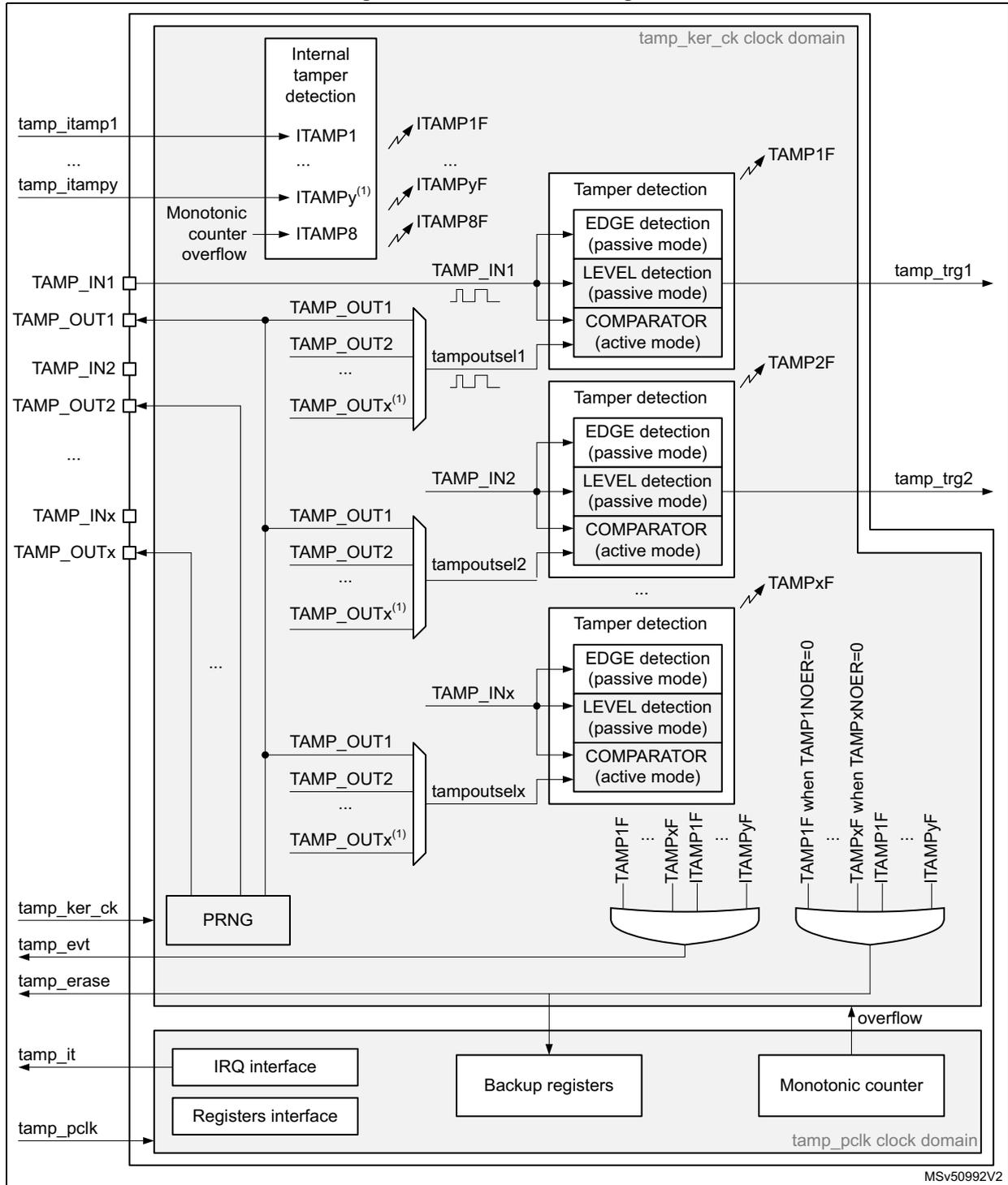
MSV50992V2
1. The number of external and internal tampers depends on products.
51.3.2 TAMP pins and internal signals
Table 366. TAMP input/output pins
| Pin name | Signal type | Description |
|---|---|---|
| TAMP_INx (x = pin index) | Input | Tamper input pin |
| TAMP_OUTx (x = pin index) | Output | Tamper output pin |
Table 367. TAMP internal input/output signals
| Internal signal name | Signal type | Description |
|---|---|---|
| tamp_ker_ck | Input | TAMP kernel clock, connected to rtc_ker_ck and also named RTCCLK in this document |
| tamp_pclk | Input | TAMP APB clock, connected to rtc_pclk |
| tamp_itamp[y] (y = signal index) | Inputs | Internal tamper event sources |
| tamp_evt | Output | Tamper event detection (internal or external) The tamp_evt is used to generate a RTC timestamp event |
| tamp_erase | Output | Device secrets erase request following tamper event detection (internal or external) |
| tamp_it | Output | TAMP interrupt (refer to Section 51.5: TAMP interrupts for details) |
| tamp_trg[x] (x = signal index) | Output | Tamper detection trigger |
The TAMP kernel clock is usually the LSE at 32.768 kHz although it is possible to select other clock sources in the RCC (refer to RCC for more details). Some detections modes are not available in some low-power modes or \( V_{BAT} \) when the selected clock is not LSE (refer to Section 51.4: TAMP low-power modes for more details).
Table 368. TAMP interconnection
| Signal name | Source/Destination |
|---|---|
| tamp_evt | rtc_tamp_evt used to generate a timestamp event |
| tamp_erase | The tamp_erase signal is used to erase the device secrets listed hereafter: backup registers, backup SRAM and OTFDEC keys & CRC registers |
| tamp_itamp1 | RTC voltage domain monitoring |
| tamp_itamp2 | Temperature monitoring |
| tamp_itamp3 | LSE monitoring |
| tamp_itamp4 | HSE monitoring |
| tamp_itamp5 | RTC calendar overflow (rtc_calovf) |
| tamp_itamp6 | ST manufacturer readout |
| tamp_itamp8 (1) | Monotonic counter overflow |
- 1. This signal is generated in the TAMP peripheral.
For GPIOs controlled by the TAMP refer to Table 359: RTC pin PC13 configuration and Table 360: PI8 configuration .
51.3.3 TAMP register write protection
After system reset, the TAMP registers (including backup registers) are protected against parasitic write access by the DBP bit in the power control peripheral (refer to the PWR power control section). DBP bit must be set in order to enable TAMP registers write access.
51.3.4 Tamper detection
The tamper detection can be configured for the following purposes:
- • erase the backup registers and the SRAMs listed in Table 368: TAMP interconnection (default configuration)
- • generate an interrupt, capable to wake up from Stop and Standby mode
- • generate a hardware trigger for the low-power timers
TAMP backup registers
The backup registers (TAMP_BKPxR) are not reset by system reset or when the device wakes up from Standby mode.
The backup registers are reset when a tamper detection event occurs except if the TAMPxNOER bit is set, or if the TAMPxMSK is set in the TAMP_CR2 register.
Note: The backup registers are also erased when the readout protection of the flash is changed from level 1 to level 0.
Tamper detection initialization
Each input can be enabled by setting the corresponding TAMPxE bits to 1 in the TAMP_CR register.
Each TAMP_INx tamper detection input is associated with a flag TAMPxF in the TAMP_SR register.
When TAMPxMSK is cleared:
The TAMPxF flag is asserted after the tamper event on the pin, with the latency provided below:
- • 3 ck_apre cycles when TAMPFLT differs from 0x0 (level detection with filtering)
- • 3 ck_apre cycles when TAMPTS = 1 (timestamp on tamper event)
- • No latency when TAMPFLT = 0x0 (edge detection) and TAMPTS = 0
A new tamper occurring on the same pin during this period and as long as TAMPxF is set cannot be detected.
When TAMPxMSK is set:
A new tamper occurring on the same pin cannot be detected during the latency described above and 2.5 ck_rtc additional cycles.
By setting the TAMPxIE bit in the TAMP_IER register, an interrupt is generated when a tamper detection event occurs (when TAMPxF is set). Setting TAMPxIE is not allowed when the corresponding TAMPxMSK is set.
Trigger output generation on tamper event
The tamper event detection can be used as trigger input by the low-power timers.
When TAMPxMSK bit is cleared in TAMP_CR register, the TAMPxF flag must be cleared by software in order to allow a new tamper detection on the same pin.
When TAMPxMSK bit is set, the TAMPxF flag is masked, and kept cleared in TAMP_SR register. This configuration allows to trig automatically the low-power timers in Stop mode, without requiring the system wake-up to perform the TAMPxF clearing. In this case, the backup registers are not cleared.
This feature is available only when the tamper is configured in the Level detection with filtering on tamper inputs (passive mode) mode (TAMPFLT \( \neq \) 00 and active mode is not selected).
Timestamp on tamper event
With TAMPTS set to 1 in the RTC_CR, any tamper event causes a timestamp to occur. In this case, either the TSF bit or the TSOVF bit is set in RTC_SR, in the same manner as if a normal timestamp event occurs. The affected tamper flag register TAMPxF is set in the TAMP_SR at the same time that TSF or TSOVF is set in the RTC_SR.
Edge detection on tamper inputs (passive mode)
If the TAMPFLT bits are 00, the TAMP_INx pins generate tamper detection events when either a rising edge/high level or a falling edge/low level is observed depending on the corresponding TAMPxTRG bit. The internal pull-up resistors on the TAMP_INx inputs are deactivated when edge detection is selected.
Caution:
When using the edge detection, it is recommended to check by software the tamper pin level just after enabling the tamper detection (by reading the GPIO registers), and before writing sensitive values in the backup registers, to ensure that an active edge did not occur before enabling the tamper event detection.
When TAMPFLT = 00 and TAMPxTRG = 0 (rising edge detection), a tamper event may be detected by hardware if the tamper input is already at high level before enabling the tamper detection.
After a tamper event has been detected and cleared, the TAMP_INx should be disabled and then re-enabled (TAMPxE set to 1) before re-programming the backup registers (TAMP_BKPxR). This prevents the application from writing to the backup registers while the TAMP_INx input value still indicates a tamper detection. This is equivalent to a level detection on the TAMP_INx input.
Note: Tamper detection is still active when \( V_{DD} \) power is switched off. To avoid unwanted resetting of the backup registers, the pin to which the TAMPx is mapped should be externally tied to the correct level.
Level detection with filtering on tamper inputs (passive mode)
Level detection with filtering is performed by setting TAMPFLT to a non-zero value. A tamper detection event is generated when either 2, 4, or 8 (depending on TAMPFLT) consecutive samples are observed at the level designated by the TAMPxTRG bits.
The TAMP_INx inputs are precharged through the I/O internal pull-up resistance before its state is sampled, unless disabled by setting TAMPPUDIS to 1. The duration of the precharge is determined by the TAMPPRCH bits, allowing for larger capacitances on the TAMP_INx inputs.
The trade-off between tamper detection latency and power consumption through the pull-up can be optimized by using TAMPFREQ to determine the frequency of the sampling for level detection.
Note: Refer to the datasheet for the electrical characteristics of the pull-up resistors.
Active tamper detection
When the TAMPxAM bit is set in the TAMP_ATCR, the tamper events are configured in active mode, which is based on a comparison between a TAMP_OUTy pin and a TAMP_INx pin. By default (ATOSHARE = 0) the comparison is made between TAMP_INx and TAMP_OUTx (y = x). When ATOSHARE bit is set, the same output can be used for several tamper inputs. Refer to ATOSHARE and ATOSEL bits descriptions in the TAMP_ATCR register.
Every two CK_ATPER cycles ( \( CK\_ATPER = 2^{ATPER} \times CK\_ATPRE = 2^{ATPER} \times 2^{ATCKSEL} \times RTCCLK \) ), TAMP_OUTy output pin provides a value provided by a pseudo random number generator (PRNG). After outputting this value, the TAMP_OUTy pin outputs its opposite value one CK_ATPER cycle after.
PRNG is consumed by the selected tamper outputs at a different frequency depending on the number of selected tamper outputs. The number of selected outputs depends on TAMPxAM, TAMPxE, ATOSEL and ATOSHARE.
- • When only 1 output is selected: PRNG is consumed every 16 CK_ATPER periods.
- • When 2 outputs are selected: PRNG is consumed every 8 CK_ATPER periods.
- • When 3 or 4 outputs are selected: PRNG is consumed every 4 CK_ATPER periods.
- • When 5 or more outputs are selected: PRNG is consumed every 2 CK_ATPER periods
The PRNG needs minimum 9 CK_ATPRE cycles to output a new value. Consequently the minimum ATPER values for correct functionality are provided in the table below:
Table 369. Minimum ATPER value
| Number of selected outputs | Minimum ATPER |
|---|---|
| 1 | 0 |
| 2 | 1 |
| 3 or 4 | 2 |
| 5 or more | 3 |
The TAMP_INx pin is externally connected to TAMP_OUTy pin. The comparison is made between TAMP_OUTy output value and TAMP_INx received value, taking into account feedback delay. In case a comparison mismatch occurs, the TAMPxF bit is set in the TAMP_SR register.
As an example, TAMP_OUT1 can be used for comparison with TAMP_IN1 and TAMP_IN2 by configuring and enabling both TAMP1 and TAMP2 in active mode, with ATOSHARE = 1, ATOSEL1 = 00 and ATOSEL2 = 00.
The active tamper can be combined with input filtering when FLTEN = 1. In this case, the tamper is detected only when 2 comparisons are false, in 4 consecutive comparison samples.
The pseudo-random generator must be initialized with a seed. This is done by writing consecutively four 32-bit random values in the TAMP_ATSEEDR register. Programming the seed automatically sends it to the PRNG. As long as the new seed is transferred and elaborated by the PRNG, the SEEDF bit is set in the TAMP_ATOR and it is not allowed to switch off the TAMP APB clock. The duration of the elaboration is up to 184 APB clock cycles after the forth seed is written. Consequently, after writing a new seed, the user must wait until SEEDF is cleared before entering low-power modes.
The active tamper outputs are activated only after the first seed is written and the elaboration is completed. Then new seeds can be written and elaborated during active tamper activity.
Active tamper initialization
Here is the software procedure to initialize the active tampers after system reset:
Read INITS in TAMP_ATOR register.
- • If INITS = 0x0 (initialization was not done):
- a) Write TAMP_ATCR to configure Active tamper clock, filter and output sharing if any, and active mode.
- b) Write TAMP_CR1 to enable tampers (all the needed tampers must be enabled in the same write access).
- c) Write SEED by writing four times in the TAMP_ATSEEDR.
- d) Wait until SEEDF = 0 in RTC_ATOR. Backup registers are then protected by active tamper.
- • If INITS = 0x1 (initialization already done):
No initialization. To increase randomness a new SEED should be provided regularly. When a new SEED is provided, wait until SEEDF = 0 before entering a low-power mode which switches off the RTC APB clock.
- • In case the tampers are disabled by software, and re-enabled afterwards, the SEED must be written after enabling tampers:
- a) Write TAMP_CR1 to enable tampers (all the needed tampers must be enabled in the same write access).
- b) Write SEED by writing four times in the TAMP_ATSEEDR.
- c) Wait until SEEDF = 0 in RTC_ATOR. Backup registers are then protected by active tamper.
Caution: The active tampers must be disabled before entering the RTC initialization mode (INIT = 1 in the RTC_ICSR). Refer to Section : Calendar initialization and configuration for more details.
51.4 TAMP low-power modes
Table 370. Effect of low-power modes on TAMP
| Mode | Description |
|---|---|
| Sleep | No effect. TAMP interrupts cause the device to exit the Sleep mode. |
| Stop | No effect on all features, except for level detection with filtering and active tamper modes which remain active only when the clock source is LSE or LSI. TAMP interrupts cause the device to exit the Stop mode. |
| Standby | No effect on all features, except for level detection with filtering and active tamper modes which remain active only when the clock source is LSE or LSI. TAMP interrupts cause the device to exit the Standby mode. |
Table 371. TAMP pins functionality over modes
| Pin name | Functional in all low-power modes | Functional in V BAT mode |
|---|---|---|
| TAMP_INx, x = 1,2 | Yes | Yes |
| TAMP_IN3 | Yes | No (1) |
| TAMP_OUTx, x = 2,3 | Yes | Yes |
1. TAMP_IN3 is mapped on PC1 that is not supplied by V BAT .
51.5 TAMP interrupts
The interrupt channel is set in the interrupt status register. The interrupt output is also activated.
Table 372. Interrupt requests
| Interrupt acronym | Interrupt event | Event flag (1) | Enable control bit (2) | Interrupt clear method | Exit from Sleep mode | Exit from Stop and Standby modes |
|---|---|---|---|---|---|---|
| RTC_TAMP_ STAMP_CSS_ LSE | Tamper x (3) | TAMPxF | TAMPxIE | Write 1 in CTAMPxF | Yes | Yes (4) |
| Internal tamper y (3) | ITAMPyF | ITAMPyIE | Write 1 in CITAMPxF | Yes | Yes (4) |
- 1. The event flags are in the TAMP_SR register.
- 2. The interrupt masked flags (resulting from event flags AND enable control bits) are in the TAMP_MISR register.
- 3. The number of tamper and internal tamper events depend on products.
- 4. In case of level detection with filtering passive tamper mode, or in case of active tamper mode, wake-up from Stop and Standby modes is possible only when the TAMP clock source is LSE or LSI.
51.6 TAMP registers
Refer to Section 1.2 on page 99 of the reference manual for a list of abbreviations used in register descriptions. The peripheral registers can be accessed by words (32-bit).
51.6.1 TAMP control register 1 (TAMP_CR1)
Address offset: 0x00
Backup domain reset value: 0xFFFF 0000
System reset: not affected
| 31 | 30 | 29 | 28 | 27 | 26 | 25 | 24 | 23 | 22 | 21 | 20 | 19 | 18 | 17 | 16 |
|---|---|---|---|---|---|---|---|---|---|---|---|---|---|---|---|
| Res. | Res. | Res. | Res. | Res. | Res. | Res. | Res. | ITAMP8 E | Res. | ITAMP6 E | ITAMP5 E | ITAMP4 E | ITAMP3 E | ITAMP2 E | ITAMP1 E |
| rw | rw | rw | rw | rw | rw | rw |
| 15 | 14 | 13 | 12 | 11 | 10 | 9 | 8 | 7 | 6 | 5 | 4 | 3 | 2 | 1 | 0 |
|---|---|---|---|---|---|---|---|---|---|---|---|---|---|---|---|
| Res. | Res. | Res. | Res. | Res. | Res. | Res. | Res. | Res. | Res. | Res. | Res. | Res. | TAMP3 E | TAMP2 E | TAMP1 E |
| rw | rw | rw |
Bits 31:24 Reserved, must be kept at reset value.
Bit 23 ITAMP8E : Internal tamper 8 enable: monotonic counter overflow
0: Internal tamper 8 disabled.
1: Internal tamper 8 enabled: a tamper is generated when the TAMP_CNT overflows.
Bit 22 Reserved, must be kept at reset value.
Bit 21 ITAMP6E : Internal tamper 6 enable: ST manufacturer readout
0: Internal tamper 6 disabled.
1: Internal tamper 6 enabled: a tamper is generated in case of ST manufacturer readout.
Bit 20 ITAMP5E : Internal tamper 5 enable: RTC calendar overflow
0: Internal tamper 5 disabled.
1: Internal tamper 5 enabled: a tamper is generated when the RTC calendar reaches its maximum value, on the 31 st of December 99, at 23:59:59. The calendar is then frozen and cannot overflow.
Bit 19 ITAMP4E : Internal tamper 4 enable: HSE monitoring
0: Internal tamper 4 disabled.
1: Internal tamper 4 enabled: a tamper is generated when the HSE frequency is below or above thresholds.
Bit 18 ITAMP3E : Internal tamper 3 enable: LSE monitoring
0: Internal tamper 3 disabled.
1: Internal tamper 3 enabled: a tamper is generated when the LSE frequency is below or above thresholds.
Bit 17 ITAMP2E : Internal tamper 2 enable: Temperature monitoring
0: Internal tamper 2 disabled.
1: Internal tamper 2 enabled: a tamper is generated when the temperature is below or above thresholds.
Bit 16 ITAMP1E : Internal tamper 1 enable: RTC power domain supply monitoring
0: Internal tamper 1 disabled.
1: Internal tamper 1 enabled: a tamper is generated when the RTC power domain supply is below or above thresholds.
Bits 15:3 Reserved, must be kept at reset value.
Bit 2 TAMP3E : Tamper detection on TAMP_IN3 enable (1)
0: Tamper detection on TAMP_IN3 is disabled.
1: Tamper detection on TAMP_IN3 is enabled.
Bit 1 TAMP2E : Tamper detection on TAMP_IN2 enable (1)
0: Tamper detection on TAMP_IN2 is disabled.
1: Tamper detection on TAMP_IN2 is enabled.
Bit 0 TAMP1E : Tamper detection on TAMP_IN1 enable (1)
0: Tamper detection on TAMP_IN1 is disabled.
1: Tamper detection on TAMP_IN1 is enabled.
- 1. Tamper detection mode (selected with TAMP_FLTCR, TAMP_ATCR1 registers and TAMPxTRG bits in TAMP_CR2), must be configured before enabling the tamper detection.
51.6.2 TAMP control register 2 (TAMP_CR2)
Address offset: 0x04
Backup domain reset value: 0x0000 0000
System reset: not affected
| 31 | 30 | 29 | 28 | 27 | 26 | 25 | 24 | 23 | 22 | 21 | 20 | 19 | 18 | 17 | 16 |
|---|---|---|---|---|---|---|---|---|---|---|---|---|---|---|---|
| Res. | Res. | Res. | Res. | Res. | TAMP3 TRG | TAMP2 TRG | TAMP1 TRG | Res. | Res. | Res. | Res. | Res. | TAMP3 MSK | TAMP2 MSK | TAMP1 MSK |
| rw | rw | rw | rw | rw | rw |
| 15 | 14 | 13 | 12 | 11 | 10 | 9 | 8 | 7 | 6 | 5 | 4 | 3 | 2 | 1 | 0 |
|---|---|---|---|---|---|---|---|---|---|---|---|---|---|---|---|
| Res. | Res. | Res. | Res. | Res. | Res. | Res. | Res. | Res. | Res. | Res. | Res. | Res. | TAMP3 NOER | TAMP2 NOER | TAMP1 NOER |
| rw | rw | rw |
Bits 31:27 Reserved, must be kept at reset value.
Bit 26 TAMP3TRG : Active level for tamper 3 input (active mode disabled)
0: If TAMPFLT ≠ 00 Tamper 3 input staying low triggers a tamper detection event.
If TAMPFLT = 00 Tamper 3 input rising edge and high level triggers a tamper detection event.
1: If TAMPFLT ≠ 00 Tamper 3 input staying high triggers a tamper detection event.
If TAMPFLT = 00 Tamper 3 input falling edge and low level triggers a tamper detection event.
Bit 25 TAMP2TRG : Active level for tamper 2 input (active mode disabled)
0: If TAMPFLT ≠ 00 Tamper 2 input staying low triggers a tamper detection event.
If TAMPFLT = 00 Tamper 2 input rising edge and high level triggers a tamper detection event.
1: If TAMPFLT ≠ 00 Tamper 2 input staying high triggers a tamper detection event.
If TAMPFLT = 00 Tamper 2 input falling edge and low level triggers a tamper detection event.
Bit 24 TAMP1TRG : Active level for tamper 1 input (active mode disabled)
0: If TAMPFLT ≠ 00 Tamper 1 input staying low triggers a tamper detection event.
If TAMPFLT = 00 Tamper 1 input rising edge and high level triggers a tamper detection event.
1: If TAMPFLT ≠ 00 Tamper 1 input staying high triggers a tamper detection event.
If TAMPFLT = 00 Tamper 1 input falling edge and low level triggers a tamper detection event.
Bit 23 Reserved, must be kept at reset value.
Bits 22:19 Reserved, must be kept at reset value.
Bit 18 TAMP3MSK : Tamper 3 mask
0: Tamper 3 event generates a trigger event and TAMP3F must be cleared by software to allow next tamper event detection.
1: Tamper 3 event generates a trigger event. TAMP3F is masked and internally cleared by hardware. The backup registers (1) are not erased.
The tamper 3 interrupt must not be enabled when TAMP3MSK is set.
Bit 17 TAMP2MSK : Tamper 2 mask
0: Tamper 2 event generates a trigger event and TAMP2F must be cleared by software to allow next tamper event detection.
1: Tamper 2 event generates a trigger event. TAMP2F is masked and internally cleared by hardware. The backup registers (1) are not erased.
The tamper 2 interrupt must not be enabled when TAMP2MSK is set.
Bit 16 TAMP1MSK : Tamper 1 mask
0: Tamper 1 event generates a trigger event and TAMP1F must be cleared by software to allow next tamper event detection.
1: Tamper 1 event generates a trigger event. TAMP1F is masked and internally cleared by hardware. The backup registers (1) are not erased.
The tamper 1 interrupt must not be enabled when TAMP1MSK is set.
Bits 15:3 Reserved, must be kept at reset value.
Bit 2 TAMP3NOER : Tamper 3 no erase
0: Tamper 3 event erases the backup registers.
1: Tamper 3 event does not erase the backup registers (1) .
Bit 1 TAMP2NOER : Tamper 2 no erase
0: Tamper 2 event erases the backup registers.
1: Tamper 2 event does not erase the backup registers (1) .
Bit 0 TAMP1NOER : Tamper 1 no erase
0: Tamper 1 event erases the backup registers.
1: Tamper 1 event does not erase the backup registers (1) .
- 1. and the device secrets erased by tamp_erase signal (refer to Table 368: TAMP interconnection ).
51.6.3 TAMP filter control register (TAMP_FLTCR)
Address offset: 0x0C
Backup domain reset value: 0x0000 0000
System reset: not affected
| 31 | 30 | 29 | 28 | 27 | 26 | 25 | 24 | 23 | 22 | 21 | 20 | 19 | 18 | 17 | 16 |
|---|---|---|---|---|---|---|---|---|---|---|---|---|---|---|---|
| Res. | Res. | Res. | Res. | Res. | Res. | Res. | Res. | Res. | Res. | Res. | Res. | Res. | Res. | Res. | Res. |
| 15 | 14 | 13 | 12 | 11 | 10 | 9 | 8 | 7 | 6 | 5 | 4 | 3 | 2 | 1 | 0 |
| Res. | Res. | Res. | Res. | Res. | Res. | Res. | Res. | TAMP PUDIS | TAMPPRCH [1:0] | TAMPFLT [1:0] | TAMPFREQ [2:0] | ||||
| rw | rw | rw | rw | rw | rw | rw | rw | ||||||||
Bits 31:8 Reserved, must be kept at reset value.
Bit 7 TAMPPUDIS : TAMP_INx pull-up disable
This bit determines if each of the TAMPx pins are precharged before each sample.
0: Precharge TAMP_INx pins before sampling (enable internal pull-up)
1: Disable precharge of TAMP_INx pins.
Bits 6:5 TAMPPRCH[1:0] : TAMP_INx precharge duration
These bits determine the duration of time during which the pull-up is activated before each sample. TAMPPRCH is valid for each of the TAMP_INx inputs.
0x0: 1 RTCCLK cycle
0x1: 2 RTCCLK cycles
0x2: 4 RTCCLK cycles
0x3: 8 RTCCLK cycles
Bits 4:3 TAMPFLT[1:0] : TAMP_INx filter count
These bits determine the number of consecutive samples at the specified level (TAMP*TRG) needed to activate a tamper event. TAMPFLT is valid for each of the TAMP_INx inputs.
0x0: Tamper event is activated on edge of TAMP_INx input transitions to the active level (no internal pull-up on TAMP_INx input).
0x1: Tamper event is activated after 2 consecutive samples at the active level.
0x2: Tamper event is activated after 4 consecutive samples at the active level.
0x3: Tamper event is activated after 8 consecutive samples at the active level.
Bits 2:0 TAMPFREQ[2:0] : Tamper sampling frequency
Determines the frequency at which each of the TAMP_INx inputs are sampled.
0x0: RTCCLK / 32768 (1 Hz when RTCCLK = 32768 Hz)
0x1: RTCCLK / 16384 (2 Hz when RTCCLK = 32768 Hz)
0x2: RTCCLK / 8192 (4 Hz when RTCCLK = 32768 Hz)
0x3: RTCCLK / 4096 (8 Hz when RTCCLK = 32768 Hz)
0x4: RTCCLK / 2048 (16 Hz when RTCCLK = 32768 Hz)
0x5: RTCCLK / 1024 (32 Hz when RTCCLK = 32768 Hz)
0x6: RTCCLK / 512 (64 Hz when RTCCLK = 32768 Hz)
0x7: RTCCLK / 256 (128 Hz when RTCCLK = 32768 Hz)
Note: This register concerns only the tamper inputs in passive mode.
51.6.4 TAMP active tamper control register 1 (TAMP_ATCR1)
Address offset: 0x10
Backup domain reset value: 0x0007 0000
System reset: not affected
| 31 | 30 | 29 | 28 | 27 | 26 | 25 | 24 | 23 | 22 | 21 | 20 | 19 | 18 | 17 | 16 |
|---|---|---|---|---|---|---|---|---|---|---|---|---|---|---|---|
| FLTEN | ATO SHARE | Res. | Res. | Res. | ATPER[2:0] | Res. | Res. | Res. | Res. | Res. | ATCKSEL[2:0] | ||||
| rw | rw | rw | rw | rw | rw | rw | rw | ||||||||
| 15 | 14 | 13 | 12 | 11 | 10 | 9 | 8 | 7 | 6 | 5 | 4 | 3 | 2 | 1 | 0 |
|---|---|---|---|---|---|---|---|---|---|---|---|---|---|---|---|
| Res. | Res. | ATOSEL3[1:0] | ATOSEL2[1:0] | ATOSEL1[1:0] | Res. | Res. | Res. | Res. | Res. | TAMP3 AM | TAMP2 AM | TAMP1 AM | |||
| rw | rw | rw | rw | rw | rw | rw | rw | rw | |||||||
Bit 31 FLTEN : Active tamper filter enable
- 0: Active tamper filtering disable
- 1: Active tamper filtering enable: a tamper event is detected when 2 comparison mismatches occur out of 4 consecutive samples.
Bit 30 ATOSHARE : Active tamper output sharing
- 0: Each active tamper input TAMP_INi is compared with its dedicated output TAMP_OUTi
- 1: Each active tamper input TAMP_INi is compared with TAMPOUTSELx as defined below, with TAMPOUTSELx defined by ATOSELx bits.
Bits 29:27 Reserved, must be kept at reset value.
Bits 26:24 ATPER[2:0] : Active tamper output change period
The tamper output is changed every \( CK\_ATPER = (2^{ATPER} \times CK\_ATPRE) \) cycles. Refer to Table 369: Minimum ATPER value .
Bits 23:19 Reserved, must be kept at reset value.
Bits 18:16 ATCKSEL[2:0] : Active tamper RTC asynchronous prescaler clock selection
These bits selects the RTC asynchronous prescaler stage output. The selected clock is CK_ATPRE.
\(
f_{CK\_ATPRE} = f_{RTCCLK} / 2^{ATCKSEL}
\)
when (PREDIV_A+1) = 128.
- 000: RTCCLK is selected
- 001: RTCCLK/2 is selected when (PREDIV_A+1) = 128 (actually selects 1 st flip flop output)
- 010: RTCCLK/4 is selected when (PREDIV_A+1) = 128 (actually selects 2 nd flip flop output)
- ...
- 111: RTCCLK/128 is selected when (PREDIV_A+1) = 128 (actually selects 7 th flip flop output)
Note: These bits can be written only when all active tampers are disabled. The write protection remains for up to 1.5 ck_atpre cycles after all the active tampers are disable.
Bits 15:14 Reserved, must be kept at reset value.
Bits 13:12 ATOSEL3[1:0] : Active tamper shared output 3 selection
- 00: TAMPOUTSEL3 = TAMP_OUT1
- 01: TAMPOUTSEL3 = TAMP_OUT2
- 10: TAMPOUTSEL3 = TAMP_OUT3
- 11:
The selected output must be available in the package pinout
Bits 11:10 ATOSEL2[1:0] : Active tamper shared output 2 selection
00: TAMPOUTSEL2 = TAMP_OUT1
01: TAMPOUTSEL2 = TAMP_OUT2
10: TAMPOUTSEL2 = TAMP_OUT3
11:
The selected output must be available in the package pinout
Bits 9:8 ATOSEL1[1:0] : Active tamper shared output 1 selection
00: TAMPOUTSEL1 = TAMP_OUT1
01: TAMPOUTSEL1 = TAMP_OUT2
10: TAMPOUTSEL1 = TAMP_OUT3
11:
The selected output must be available in the package pinout
Bits 7:3 Reserved, must be kept at reset value.
Bit 2 TAMP3AM : Tamper 3 active mode
0: Tamper 3 detection mode is passive.
1: Tamper 3 detection mode is active.
Bit 1 TAMP2AM : Tamper 2 active mode
0: Tamper 2 detection mode is passive.
1: Tamper 2 detection mode is active.
Bit 0 TAMP1AM : Tamper 1 active mode
0: Tamper 1 detection mode is passive.
1: Tamper 1 detection mode is active.
Note: Changing the active tampers configuration in this register is not allowed when a TAMPxAM bit is set, unless the corresponding TAMPxE bits are all cleared in the TAMP_CR1 register.
All tampers configured in active mode must be enabled at the same time (by setting all related TAMPxE in the same TAMP_CR1 write).
All tampers configured in active mode must be disabled at the same time (by clearing all related TAMPxE in the same TAMP_CR1 write).
A minimum duration of 1 CK_ATPRE period must be waited for after disabling the active tampers and before re-enabling them.
51.6.5 TAMP active tamper seed register (TAMP_ATSEEDR)
Address offset: 0x14
Backup domain reset value: 0x0000 0000
System reset: not affected
| 31 | 30 | 29 | 28 | 27 | 26 | 25 | 24 | 23 | 22 | 21 | 20 | 19 | 18 | 17 | 16 |
| SEED[31:16] | |||||||||||||||
| w | w | w | w | w | w | w | w | w | w | w | w | w | w | w | w |
| 15 | 14 | 13 | 12 | 11 | 10 | 9 | 8 | 7 | 6 | 5 | 4 | 3 | 2 | 1 | 0 |
| SEED[15:0] | |||||||||||||||
| w | w | w | w | w | w | w | w | w | w | w | w | w | w | w | w |
Bits 31:0 SEED[31:0] : Pseudo-random generator seed value
This register must be written four times with 32-bit values to provide the 128-bit seed to the PRNG. Writing to this register automatically sends the seed value to the PRNG.
51.6.6 TAMP active tamper output register (TAMP_ATOR)
Address offset: 0x18
Backup domain reset value: 0x0000 0000
System reset: not affected, except for SEEDF which is reset to 0.
| 31 | 30 | 29 | 28 | 27 | 26 | 25 | 24 | 23 | 22 | 21 | 20 | 19 | 18 | 17 | 16 |
|---|---|---|---|---|---|---|---|---|---|---|---|---|---|---|---|
| Res. | Res. | Res. | Res. | Res. | Res. | Res. | Res. | Res. | Res. | Res. | Res. | Res. | Res. | Res. | Res. |
| 15 | 14 | 13 | 12 | 11 | 10 | 9 | 8 | 7 | 6 | 5 | 4 | 3 | 2 | 1 | 0 |
| INITS | SEEDF | Res. | Res. | Res. | Res. | Res. | Res. | PRNG[7:0] | |||||||
| r | r | r | r | r | r | r | r | r | r | ||||||
Bits 31:16 Reserved, must be kept at reset value.
Bit 15 INITS : Active tamper initialization status
This flag is set by hardware when the PRNG has absorbed the first 128-bit seed, meaning that the enabled active tamper are functional. This flag is left unchanged when the active tamper are disabled.
Bit 14 SEEDF : Seed running flag
This flag is set by hardware when a new seed is written in the TAMP_ATSEEDR. It is cleared by hardware when the PRNG has absorbed this new seed, and by system reset. The TAMP APB clock must not be switched off as long as SEEDF is set.
Bits 13:8 Reserved, must be kept at reset value.
Bits 7:0 PRNG[7:0] : Pseudo-random generator value
This field provides the values of the PRNG output. Because of potential inconsistencies due to synchronization delays, PRNG must be read at least twice. The read value is correct if it is equal to previous read value.
51.6.7 TAMP interrupt enable register (TAMP_IER)
Address offset: 0x2C
Backup domain reset value: 0x0000 0000
System reset: not affected
| 31 | 30 | 29 | 28 | 27 | 26 | 25 | 24 | 23 | 22 | 21 | 20 | 19 | 18 | 17 | 16 |
|---|---|---|---|---|---|---|---|---|---|---|---|---|---|---|---|
| Res. | Res. | Res. | Res. | Res. | Res. | Res. | Res. | ITAMP8 IE | Res. | ITAMP6 IE | ITAMP5 IE | ITAMP4 IE | ITAMP3 IE | ITAMP2 IE | ITAMP1 IE |
| rw | rw | rw | rw | rw | rw | rw | |||||||||
| 15 | 14 | 13 | 12 | 11 | 10 | 9 | 8 | 7 | 6 | 5 | 4 | 3 | 2 | 1 | 0 |
| Res. | Res. | Res. | Res. | Res. | Res. | Res. | Res. | Res. | Res. | Res. | Res. | Res. | TAMP 3IE | TAMP 2IE | TAMP 1IE |
| rw | rw | rw |
Bits 31:24 Reserved, must be kept at reset value.
Bit 23 ITAMP8IE : Internal tamper 8 interrupt enable: monotonic counter overflow
0: Internal tamper 8 interrupt disabled.
1: Internal tamper 8 interrupt enabled.
Bit 22 Reserved, must be kept at reset value.
Bit 21 ITAMP6IE : Internal tamper 6 interrupt enable: ST manufacturer readout
0: Internal tamper 6 interrupt disabled.
1: Internal tamper 6 interrupt enabled.
Bit 20 ITAMP5IE : Internal tamper 5 interrupt enable: RTC calendar overflow
0: Internal tamper 5 interrupt disabled.
1: Internal tamper 5 interrupt enabled.
Bit 19 ITAMP4IE : Internal tamper 4 interrupt enable: HSE monitoring
0: Internal tamper 4 interrupt disabled.
1: Internal tamper 4 interrupt enabled.
Bit 18 ITAMP3IE : Internal tamper 3 interrupt enable: LSE monitoring
0: Internal tamper 3 interrupt disabled.
1: Internal tamper 3 interrupt enabled.
Bit 17 ITAMP2IE : Internal tamper 2 interrupt enable: Temperature monitoring
0: Internal tamper 2 interrupt disabled.
1: Internal tamper 2 interrupt enabled.
Bit 16 ITAMP1IE : Internal tamper 1 interrupt enable: RTC power domain supply monitoring
0: Internal tamper 1 interrupt disabled.
1: Internal tamper 1 interrupt enabled
Bits 15:3 Reserved, must be kept at reset value.
Bit 2 TAMP3IE : Tamper 3 interrupt enable
0: Tamper 3 interrupt disabled.
1: Tamper 3 interrupt enabled..
Bit 1 TAMP2IE : Tamper 2 interrupt enable
0: Tamper 2 interrupt disabled.
1: Tamper 2 interrupt enabled.
Bit 0 TAMP1IE : Tamper 1 interrupt enable
0: Tamper 1 interrupt disabled.
1: Tamper 1 interrupt enabled.
51.6.8 TAMP status register (TAMP_SR)
Address offset: 0x30
Backup domain reset value: 0x0000 0000
System reset: not affected
| 31 | 30 | 29 | 28 | 27 | 26 | 25 | 24 | 23 | 22 | 21 | 20 | 19 | 18 | 17 | 16 |
|---|---|---|---|---|---|---|---|---|---|---|---|---|---|---|---|
| Res. | Res. | Res. | Res. | Res. | Res. | Res. | Res. | ITAMP8F | Res. | ITAMP6F | ITAMP5F | ITAMP4F | ITAMP3F | ITAMP2F | ITAMP1F |
| r | r | r | r | r | r | r | |||||||||
| 15 | 14 | 13 | 12 | 11 | 10 | 9 | 8 | 7 | 6 | 5 | 4 | 3 | 2 | 1 | 0 |
| Res. | Res. | Res. | Res. | Res. | Res. | Res. | Res. | Res. | Res. | Res. | Res. | Res. | TAMP3F | TAMP2F | TAMP1F |
| r | r | r |
Bits 31:24 Reserved, must be kept at reset value.
Bit 23 ITAMP8F : Monotonic counter overflow tamper flag
This flag is set by hardware when a tamper detection event is detected on the internal tamper 8.
Bit 22 Reserved, must be kept at reset value.
Bit 21 ITAMP6F : ST manufacturer readout tamper detection flag
This flag is set by hardware when a tamper detection event is detected on the internal tamper 6.
Bit 20 ITAMP5F : RTC calendar overflow tamper detection flag
This flag is set by hardware when a tamper detection event is detected on the internal tamper 5.
Bit 19 ITAMP4F : HSE monitoring tamper detection flag
This flag is set by hardware when a tamper detection event is detected on the internal tamper 4.
Bit 18 ITAMP3F : LSE monitoring tamper detection flag
This flag is set by hardware when a tamper detection event is detected on the internal tamper 3.
Bit 17 ITAMP2F : Temperature monitoring tamper detection flag
This flag is set by hardware when a tamper detection event is detected on the internal tamper 2.
Bit 16 ITAMP1F : RTC power domain voltage monitoring tamper detection flag
This flag is set by hardware when a tamper detection event is detected on the internal tamper 1.
Bits 15:3 Reserved, must be kept at reset value.
Bit 2 TAMP3F : TAMP3 detection flag
This flag is set by hardware when a tamper detection event is detected on the TAMP3 input.
Bit 1 TAMP2F : TAMP2 detection flag
This flag is set by hardware when a tamper detection event is detected on the TAMP2 input.
Bit 0 TAMP1F : TAMP1 detection flag
This flag is set by hardware when a tamper detection event is detected on the TAMP1 input.
51.6.9 TAMP masked interrupt status register (TAMP_MISR)
Address offset: 0x34
Backup domain reset value: 0x0000 0000
System reset: not affected
| 31 | 30 | 29 | 28 | 27 | 26 | 25 | 24 | 23 | 22 | 21 | 20 | 19 | 18 | 17 | 16 |
|---|---|---|---|---|---|---|---|---|---|---|---|---|---|---|---|
| Res. | Res. | Res. | Res. | Res. | Res. | Res. | Res. | ITAMP8 MF | Res. | ITAMP6 MF | ITAMP5 MF | ITAMP4 MF | ITAMP3 MF | ITAMP2 MF | ITAMP1 MF |
| r | r | r | r | r | r | r | |||||||||
| 15 | 14 | 13 | 12 | 11 | 10 | 9 | 8 | 7 | 6 | 5 | 4 | 3 | 2 | 1 | 0 |
| Res. | Res. | Res. | Res. | Res. | Res. | Res. | Res. | Res. | Res. | Res. | Res. | Res. | TAMP 3MF | TAMP 2MF | TAMP 1MF |
| r | r | r |
Bits 31:24 Reserved, must be kept at reset value.
Bit 23 ITAMP8MF : Monotonic counter overflow interrupt masked flag
This flag is set by hardware when the internal tamper 8 interrupt is raised.
Bit 22 Reserved, must be kept at reset value.
Bit 21 ITAMP6MF : ST manufacturer readout tamper interrupt masked flag
This flag is set by hardware when the internal tamper 6 interrupt is raised.
Bit 20 ITAMP5MF : RTC calendar overflow tamper interrupt masked flag
This flag is set by hardware when the internal tamper 5 interrupt is raised.
Bit 19 ITAMP4MF : HSE monitoring tamper interrupt masked flag
This flag is set by hardware when the internal tamper 4 interrupt is raised.
Bit 18 ITAMP3MF : LSE monitoring tamper interrupt masked flag
This flag is set by hardware when the internal tamper 3 interrupt is raised.
Bit 17 ITAMP2MF : Temperature monitoring tamper interrupt masked flag
This flag is set by hardware when the internal tamper 2 interrupt is raised.
Bit 16 ITAMP1MF : RTC power domain voltage monitoring tamper interrupt masked flag
This flag is set by hardware when the internal tamper 1 interrupt is raised.
Bits 15:3 Reserved, must be kept at reset value.
Bit 2 TAMP3MF : TAMP3 interrupt masked flag
This flag is set by hardware when the tamper 3 interrupt is raised.
Bit 1 TAMP2MF : TAMP2 interrupt masked flag
This flag is set by hardware when the tamper 2 interrupt is raised.
Bit 0 TAMP1MF : TAMP1 interrupt masked flag
This flag is set by hardware when the tamper 1 interrupt is raised.
51.6.10 TAMP status clear register (TAMP_SCR)
Address offset: 0x3C
System reset value: 0x0000 0000
| 31 | 30 | 29 | 28 | 27 | 26 | 25 | 24 | 23 | 22 | 21 | 20 | 19 | 18 | 17 | 16 |
|---|---|---|---|---|---|---|---|---|---|---|---|---|---|---|---|
| Res. | Res. | Res. | Res. | Res. | Res. | Res. | Res. | C ITAMP 8F | Res. | C ITAMP 6F | C ITAMP 5F | C ITAMP 4F | C ITAMP 3F | C ITAMP 2F | C ITAMP 1F |
| w | w | w | w | w | w | w | |||||||||
| 15 | 14 | 13 | 12 | 11 | 10 | 9 | 8 | 7 | 6 | 5 | 4 | 3 | 2 | 1 | 0 |
| Res. | Res. | Res. | Res. | Res. | Res. | Res. | Res. | Res. | Res. | Res. | Res. | Res. | CTAMP 3F | CTAMP 2F | CTAMP 1F |
| w | w | w |
Bits 31:24 Reserved, must be kept at reset value.
Bit 23 CITAMP8F : Clear ITAMP8 detection flag
Writing 1 in this bit clears the ITAMP8F bit in the TAMP_SR register.
Bit 22 Reserved, must be kept at reset value.
Bit 21 CITAMP6F : Clear ITAMP6 detection flag
Writing 1 in this bit clears the ITAMP6F bit in the TAMP_SR register.
Bit 20 CITAMP5F : Clear ITAMP5 detection flag
Writing 1 in this bit clears the ITAMP5F bit in the TAMP_SR register.
Bit 19 CITAMP4F : Clear ITAMP4 detection flag
Writing 1 in this bit clears the ITAMP4F bit in the TAMP_SR register.
Bit 18 CITAMP3F : Clear ITAMP3 detection flag
Writing 1 in this bit clears the ITAMP3F bit in the TAMP_SR register.
Bit 17 CITAMP2F : Clear ITAMP2 detection flag
Writing 1 in this bit clears the ITAMP2F bit in the TAMP_SR register.
Bit 16 CITAMP1F : Clear ITAMP1 detection flag
Writing 1 in this bit clears the ITAMP1F bit in the TAMP_SR register.
Bits 15:3 Reserved, must be kept at reset value.
Bit 2 CTAMP3F : Clear TAMP3 detection flag
Writing 1 in this bit clears the TAMP3F bit in the TAMP_SR register.
Bit 1 CTAMP2F : Clear TAMP2 detection flag
Writing 1 in this bit clears the TAMP2F bit in the TAMP_SR register.
Bit 0 CTAMP1F : Clear TAMP1 detection flag
Writing 1 in this bit clears the TAMP1F bit in the TAMP_SR register.
51.6.11 TAMP monotonic counter register (TAMP_COUNTR)
Address offset: 0x040
Backup domain reset value: 0x0000 0000
System reset: not affected
| 31 | 30 | 29 | 28 | 27 | 26 | 25 | 24 | 23 | 22 | 21 | 20 | 19 | 18 | 17 | 16 |
|---|---|---|---|---|---|---|---|---|---|---|---|---|---|---|---|
| COUNT[31:16] | |||||||||||||||
| r | r | r | r | r | r | r | r | r | r | r | r | r | r | r | r |
| 15 | 14 | 13 | 12 | 11 | 10 | 9 | 8 | 7 | 6 | 5 | 4 | 3 | 2 | 1 | 0 |
| COUNT[15:0] | |||||||||||||||
| r | r | r | r | r | r | r | r | r | r | r | r | r | r | r | r |
Bits 31:0 COUNT[31:0]
This register is read-only only and is incremented by one when a write access is done to this register. This register cannot roll-over and is frozen when reaching the maximum value.
51.6.12 TAMP configuration register (TAMP_CFGR)
Address offset: 0x50
Backup domain reset value: 0x0000 0000
System reset: not affected
| 31 | 30 | 29 | 28 | 27 | 26 | 25 | 24 | 23 | 22 | 21 | 20 | 19 | 18 | 17 | 16 |
|---|---|---|---|---|---|---|---|---|---|---|---|---|---|---|---|
| Res. | Res. | Res. | Res. | Res. | Res. | Res. | Res. | Res. | Res. | Res. | Res. | Res. | Res. | Res. | Res. |
| 15 | 14 | 13 | 12 | 11 | 10 | 9 | 8 | 7 | 6 | 5 | 4 | 3 | 2 | 1 | 0 |
| Res. | Res. | Res. | Res. | Res. | Res. | Res. | Res. | Res. | Res. | Res. | Res. | Res. | Res. | Res. | OUT3_RMP |
| rw | |||||||||||||||
Bits 31:4 Reserved, must be kept at reset value.
Bits 3:1 Reserved, must be kept at reset value.
Bit 0 OUT3_RMP : TAMP_OUT3 mapping
0x0: TAMP_OUT3 is mapped on PI8
0x1: TAMP_OUT3 is mapped on PC13
51.6.13 TAMP backup x register (TAMP_BKPxR)
Address offset: \( 0x100 + 0x04 * x \) , ( \( x = 0 \) to \( 31 \) )
Backup domain reset value: \( 0x0000\ 0000 \)
System reset: not affected
| 31 | 30 | 29 | 28 | 27 | 26 | 25 | 24 | 23 | 22 | 21 | 20 | 19 | 18 | 17 | 16 |
|---|---|---|---|---|---|---|---|---|---|---|---|---|---|---|---|
| BKP[31:16] | |||||||||||||||
| rw | rw | rw | rw | rw | rw | rw | rw | rw | rw | rw | rw | rw | rw | rw | rw |
| 15 | 14 | 13 | 12 | 11 | 10 | 9 | 8 | 7 | 6 | 5 | 4 | 3 | 2 | 1 | 0 |
| BKP[15:0] | |||||||||||||||
| rw | rw | rw | rw | rw | rw | rw | rw | rw | rw | rw | rw | rw | w | rw | rw |
Bits 31:0 BKP[31:0]
The application can write or read data to and from these registers.
They are powered-on by \( V_{BAT} \) when \( V_{DD} \) is switched off, so that they are not reset by System reset, and their contents remain valid when the device operates in low-power mode.
In the default configuration this register is reset on a tamper detection event. It is forced to reset value as long as there is at least one internal or external tamper flag being set. This register is also reset when the readout protection (RDP) is disabled.
51.6.14 TAMP register map
Table 373. TAMP register map and reset values
| Offset | Register | 31 | 30 | 29 | 28 | 27 | 26 | 25 | 24 | 23 | 22 | 21 | 20 | 19 | 18 | 17 | 16 | 15 | 14 | 13 | 12 | 11 | 10 | 9 | 8 | 7 | 6 | 5 | 4 | 3 | 2 | 1 | 0 |
|---|---|---|---|---|---|---|---|---|---|---|---|---|---|---|---|---|---|---|---|---|---|---|---|---|---|---|---|---|---|---|---|---|---|
| 0x00 | TAMP_CR1 | Res. | Res. | Res. | Res. | Res. | Res. | Res. | Res. | ITAMP8E | Res. | ITAMP6E | ITAMP5E | ITAMP4E | ITAMP3E | ITAMP2E | ITAMP1E | Res. | Res. | Res. | Res. | Res. | Res. | Res. | Res. | Res. | Res. | Res. | Res. | Res. | TAMP3E | TAMP2E | TAMP1E |
| Reset value | 1 | 1 | 1 | 1 | 1 | 1 | 1 | 0 | 0 | 0 | |||||||||||||||||||||||
| 0x04 | TAMP_CR2 | Res. | Res. | Res. | Res. | Res. | TAMP3TRG | TAMP2TRG | TAMP1TRG | Res. | Res. | Res. | Res. | Res. | TAMP3MSK | TAMP2MSK | TAMP1MSK | Res. | Res. | Res. | Res. | Res. | Res. | Res. | Res. | Res. | Res. | Res. | Res. | Res. | TAMP3NOER | TAMP2NOER | TAMP1NOER |
| Reset value | 0 | 0 | 0 | 0 | 0 | 0 | 0 | 0 | 0 | ||||||||||||||||||||||||
| 0x0C | TAMP_FLTCR | Res. | Res. | Res. | Res. | Res. | Res. | Res. | Res. | Res. | Res. | Res. | Res. | Res. | Res. | Res. | Res. | Res. | Res. | Res. | Res. | Res. | Res. | Res. | Res. | TAMPPUDIS | TAMPPRCH[1:0] | TAMPFLT[1:0] | TAMPFREQ[2:0] | ||||
| Reset value | 0 | 0 | 0 | 0 | 0 | 0 | 0 | 0 | |||||||||||||||||||||||||
| 0x10 | TAMP_ATCR1 | FLTEN | ATOSHARE | Res. | Res. | Res. | AT-PER[2:0] | Res. | Res. | Res. | Res. | Res. | ATCK-SEL[2:0] | Res. | Res. | Res. | ATO SEL3 [1:0] | ATO SEL2 [1:0] | ATO SEL1 [1:0] | Res. | Res. | Res. | TAMP3AM | TAMP2AM | TAMP1AM | ||||||||
| Reset value | 0 | 0 | 0 | 0 | 0 | 1 | 1 | 1 | 0 | 0 | 0 | 0 | 0 | 0 | 0 | 0 | 0 | ||||||||||||||||
| 0x14 | TAMP_ATSEEDR | SEED[31:0] | |||||||||||||||||||||||||||||||
| Reset value | 0 | 0 | 0 | 0 | 0 | 0 | 0 | 0 | 0 | 0 | 0 | 0 | 0 | 0 | 0 | 0 | 0 | 0 | 0 | 0 | 0 | 0 | 0 | 0 | 0 | 0 | 0 | 0 | 0 | 0 | 0 | 0 | |
| 0x18 | TAMP_ATOR | Res. | Res. | Res. | Res. | Res. | Res. | Res. | Res. | Res. | Res. | Res. | Res. | Res. | Res. | Res. | Res. | INITS | SEEDF | Res. | Res. | Res. | Res. | Res. | Res. | PRNG[7:0] | |||||||
| Reset value | 0 | 0 | 0 | 0 | 0 | 0 | 0 | 0 | 0 | 0 | |||||||||||||||||||||||
| 0x2C | TAMP_IER | Res. | Res. | Res. | Res. | Res. | Res. | Res. | Res. | ITAMP8IE | Res. | ITAMP6IE | ITAMP5IE | ITAMP4IE | ITAMP3IE | ITAMP2IE | ITAMP1IE | Res. | Res. | Res. | Res. | Res. | Res. | Res. | Res. | Res. | Res. | Res. | Res. | Res. | TAMP3IE | TAMP2IE | TAMP1IE |
| Reset value | 0 | 0 | 0 | 0 | 0 | 0 | 0 | 0 | 0 | 0 | |||||||||||||||||||||||
| 0x30 | TAMP_SR | Res. | Res. | Res. | Res. | Res. | Res. | Res. | Res. | ITAMP8F | Res. | ITAMP6F | ITAMP5F | ITAMP4F | ITAMP3F | ITAMP2F | ITAMP1F | Res. | Res. | Res. | Res. | Res. | Res. | Res. | Res. | Res. | Res. | Res. | Res. | Res. | TAMP3F | TAMP2F | TAMP1F |
| Reset value | 0 | 0 | 0 | 0 | 0 | 0 | 0 | 0 | 0 | 0 | |||||||||||||||||||||||
| 0x34 | TAMP_MISR | Res. | Res. | Res. | Res. | Res. | Res. | Res. | Res. | ITAMP8MF | Res. | ITAMP6MF | ITAMP5MF | ITAMP4MF | ITAMP3MF | ITAMP2MF | ITAMP1MF | Res. | Res. | Res. | Res. | Res. | Res. | Res. | Res. | Res. | Res. | Res. | Res. | Res. | TAMP3MF | TAMP2MF | TAMP1MF |
| Reset value | 0 | 0 | 0 | 0 | 0 | 0 | 0 | 0 | 0 | 0 | |||||||||||||||||||||||
| 0x3C | TAMP_SCR | Res. | Res. | Res. | Res. | Res. | Res. | Res. | Res. | CITAMP8F | Res. | CITAMP6F | CITAMP5F | CITAMP4F | CITAMP3F | CITAMP2F | CITAMP1F | Res. | Res. | Res. | Res. | Res. | Res. | Res. | Res. | Res. | Res. | Res. | Res. | Res. | CTAMP3F | CTAMP2F | CTAMP1F |
| Reset value | 0 | 0 | 0 | 0 | 0 | 0 | 0 | 0 | 0 | 0 | |||||||||||||||||||||||
| 0x40 | TAMP_COUNTR | COUNT[31:0] | |||||||||||||||||||||||||||||||
| Reset value | 0 | 0 | 0 | 0 | 0 | 0 | 0 | 0 | 0 | 0 | 0 | 0 | 0 | 0 | 0 | 0 | 0 | 0 | 0 | 0 | 0 | 0 | 0 | 0 | 0 | 0 | 0 | 0 | 0 | 0 | 0 | 0 | |
Table 373. TAMP register map and reset values (continued)
| Offset | Register | 31 | 30 | 29 | 28 | 27 | 26 | 25 | 24 | 23 | 22 | 21 | 20 | 19 | 18 | 17 | 16 | 15 | 14 | 13 | 12 | 11 | 10 | 9 | 8 | 7 | 6 | 5 | 4 | 3 | 2 | 1 | 0 | |
|---|---|---|---|---|---|---|---|---|---|---|---|---|---|---|---|---|---|---|---|---|---|---|---|---|---|---|---|---|---|---|---|---|---|---|
| 0x50 | TAMP_CFGGR | Res. | Res. | Res. | Res. | Res. | Res. | Res. | Res. | Res. | Res. | Res. | Res. | Res. | Res. | Res. | Res. | Res. | Res. | Res. | Res. | Res. | Res. | Res. | Res. | Res. | Res. | Res. | Res. | Res. | Res. | Res. | Res. | OUT3_RM |
| Reset value | 0 | |||||||||||||||||||||||||||||||||
| 0x100 + 0x04*x, (x = 0 to 31) | TAMP_BKPxR | BKP[31:0] | ||||||||||||||||||||||||||||||||
| Reset value | 0 | 0 | 0 | 0 | 0 | 0 | 0 | 0 | 0 | 0 | 0 | 0 | 0 | 0 | 0 | 0 | 0 | 0 | 0 | 0 | 0 | 0 | 0 | 0 | 0 | 0 | 0 | 0 | 0 | 0 | 0 | 0 | ||
Refer to Section 2.3 on page 131 for the register boundary addresses.