21. Chrom-GRC (GFXMMU)
21.1 Introduction
The graphic MMU is a graphical oriented memory management unit aimed to:
- • Optimize memory usage according to the display shape
- • Cache linear accesses to the frame buffer
- • Prefetch data
21.2 GFXMMU main features
- • Fully programmable display shape to physically store only the visible pixel
- • Up to 4 virtual buffers
- • Each virtual buffer have 3072 or 4096 bytes per line and 1024 lines
- • Each virtual buffer can be physically mapped to any system memory
- • Optional cache for linear accesses
- • Cache can be locked to a virtual buffer
- • Cache prefetch mechanism for linear accesses anticipation
- • Interrupt in case of buffer overflow (1 per buffer)
- • Interrupt in case of memory transfer error
21.3 GFXMMU functional and architectural description
The GFXMMU is composed of two main blocks:
- • The MMU, responsible of address resolution
- • The cache, responsible of data/address caching, prefetching and packing/unpacking
Figure 101. GFXMMU block diagram
![Figure 101. GFXMMU block diagram. The diagram shows the internal architecture of the GFXMMU. An external signal AHBSlaveAdd[23:0] enters the top of the main block. Inside, a 'Cache' block and an 'MMU' block are connected. The Cache sends 'Add[23:4]' to the MMU, which responds with 'PhyAdd[22:4]' and a 'Valid' signal. The Cache also outputs 'PhyAdd[22:0]'. Below the Cache is a vertical stack of four registers: 'pBuffer3AddMSB[31:23]', 'pBuffer2AddMSB[31:23]', 'pBuffer1AddMSB[31:23]', and 'pBuffer0AddMSB[31:23]'. The Cache sends 'Add[23:22]' to these registers. To the right of the registers are 'Status registers' and 'Control registers'. An 'Overflow' signal from the MMU goes to the Status registers. The bottom output of the main block is 'AHBMasterAdd[31:0]'. A small identifier 'MSV41699V1' is in the bottom right corner.](/RM0455-STM32H7A3-7B3-7B0/5bebee42f4bee7de5eed321b4babafa0_img.jpg)
21.3.1 Virtual memory
The GFXMMU provides a virtual memory space seen by the system masters (a) . This virtual memory space is divided into four virtual buffers.
Virtual buffer
A virtual buffer is seen by any system master as a continuous memory space representing a virtual frame buffer of 1024 lines.
Each line is divided into 192 or 256 16-byte blocks depending on the 192BM bit of the GFXMMU configuration register (GFXMMU_CR).
Depending on the display shape and size, only the necessary blocks are mapped to a physical memory location. This mapping is done programming the LUT entry for each line:
- • The enable of the line
- • The number of the first “visible” block
- • The number of the last “visible” block
- • The address offset of the line within the physical buffer
The “visible” blocks can be arranged in the physical buffer in a continuous way programming the address offset of each line.
a. Refer to section “System architecture” for system masters accessing GFXMMU.
The LUT is common to all the buffers i.e. all the buffers have the same “shape”.
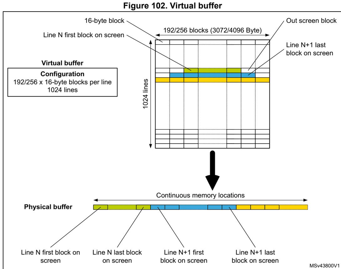
Figure 102. Virtual buffer
The diagram illustrates the mapping of a virtual buffer to a physical buffer. The virtual buffer is shown as a grid of 1024 lines and 192/256 blocks per line. The physical buffer is shown as a continuous memory location. Arrows indicate the mapping of specific blocks from the virtual buffer to the physical buffer.
Virtual buffer Configuration
192/256 x 16-byte blocks per line
1024 lines
Physical buffer
Labels in the diagram include: 16-byte block, Line N first block on screen, 192/256 blocks (3072/4096 Byte), Out screen block, Line N+1 last block on screen, Continuous memory locations, Line N first block on screen, Line N last block on screen, Line N+1 first block on screen, Line N+1 last block on screen, and MSV43800V1.
Virtual buffer overview
For a frame buffer coded in 32 bpp or 16 bpp, the virtual buffer can be configured to have 192 or 256 blocks. This results in a virtual frame buffer of 768 x 1024 or 1024 x 1024 pixels for 32 bpp and 1536 x 1024 or 2048 x 1024 for 16 bpp.
For a frame buffer coded in 24 bpp, the virtual buffer must be configured to have 192 blocks to have an integer number of pixel per lines. This results in a virtual frame buffer of 1024 x 1024 pixels for 24 bpp.
Each buffer can be physically mapped anywhere in the physical memory thanks to:
- • The physical buffer base address (PBBA) field of the GFXMMU buffer x configuration register (GFXMMU_BxCR). It configures the physical location of the 8-Mbyte area where the buffer is mapped.
- • The physical buffer location respective to the physical buffer base address is defined by the physical buffer offset (PBO) field of the GFXMMU buffer x configuration register (GFXMMU_BxCR).
Figure 103. Virtual buffer and physical buffer memory map
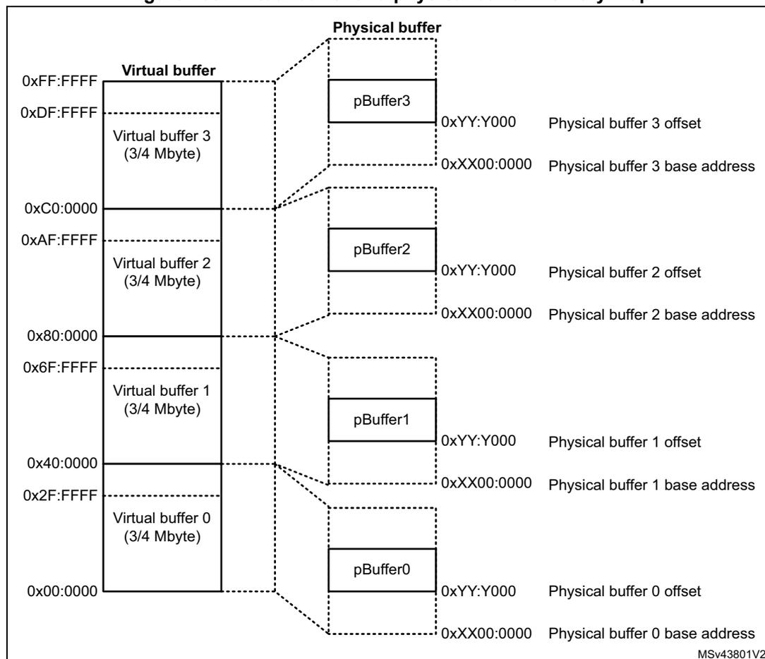
The diagram illustrates the memory mapping between virtual and physical buffers. It consists of two main columns: 'Virtual buffer' and 'Physical buffer'.
- Virtual buffer column:
- Address range 0x00:0000 to 0x2F:FFFF: Virtual buffer 0 (3/4 Mbyte)
- Address range 0x40:0000 to 0x6F:FFFF: Virtual buffer 1 (3/4 Mbyte)
- Address range 0x80:0000 to 0xAF:FFFF: Virtual buffer 2 (3/4 Mbyte)
- Address range 0xC0:0000 to 0xFF:FFFF: Virtual buffer 3 (3/4 Mbyte)
- Physical buffer column:
- pBuffer0: Associated with Virtual buffer 0. It has an offset at 0xYY:Y000 and a base address at 0xXX00:0000.
- pBuffer1: Associated with Virtual buffer 1. It has an offset at 0xYY:Y000 and a base address at 0xXX00:0000.
- pBuffer2: Associated with Virtual buffer 2. It has an offset at 0xYY:Y000 and a base address at 0xXX00:0000.
- pBuffer3: Associated with Virtual buffer 3. It has an offset at 0xYY:Y000 and a base address at 0xXX00:0000.
Dashed lines connect each virtual buffer to its corresponding physical buffer. The text 'MSv43801V2' is visible in the bottom right corner of the diagram.
The buffer can not overflow the 8-Mbyte boundary of the zone defined by its base address. In case of overflow, the buffer x overflow flag (BxOF) of the GFXMMU status register (GFXMMU_SR) is set and an interrupt is generated if the buffer x overflow interrupt enable (BxOIE) bit of the GFXMMU configuration register (GFXMMU_CR) is set.
Virtual buffer application use case
As the physical locations are independently configurable, the four virtual buffers can be physically mapped to non continuous locations. This would allow for example to have the four buffers mapped on to four different SDRAM banks and avoid extra precharge cycles accessing the SDRAM.
As a consequence, one buffer must be used by the CPU/Chrom ART for frame buffer calculation while an other one must be used by the LTDC.
The two remaining buffers can be used as a graphical library requiring extra drawing buffers.
21.3.2 MMU architecture
The MMU block is responsible of the address resolution. It receives the 24-bit address and returns the physical 23-bit address and a valid signals to indicate the address is physically mapped or not. The MMU also checks overflow of a area boundary.
The MMU LUT is implemented as a 1024 x 35-bit RAM
Figure 104. MMU block diagram
![Figure 104. MMU block diagram. The diagram shows the internal architecture of the MMU. An input address Add[23:4] is split into three main components: a Line/block decoder, a LookUp RAM, and a pBufferOffset block. The Line/block decoder takes Add[21:4] and produces Block[7:0] and Line[9:0]. The LookUp RAM is a 1024 x 35-bit memory that takes Line[9:0] and produces Block0Offset[21:4], LineEnable, FirstBlock[7:0], and LastBlock[7:0]. The pBufferOffset block takes Add[23:22] and produces pBufferOffset[22:4]. The Block0Offset[21:4] and pBufferOffset[22:4] are combined in an adder (+) to produce a 21:4 bit value. This value is then compared in a comparator (C) along with the LineEnable, FirstBlock[7:0], and LastBlock[7:0] signals from the LookUp RAM. The comparator outputs Overflow, PhyAdd[22:4], and Valid signals. A 'Block valid comp.' block is also shown, which takes FirstBlock[7:0] and LastBlock[7:0] as inputs. The diagram is labeled MSv43802V1.](/RM0455-STM32H7A3-7B3-7B0/dce73dd351f7f7311c180a56f27bb7e4_img.jpg)
Line block decoder
The line block decoder is generating the block number and the line number according the address.
Look up RAM
The look up RAM is a 1024 x 35-bit RAM with the following fields:
- • 1-bit line enable
- • 8-bit first valid block
- • 8-bit last valid block
- • 18-bit for line offset
As the RAM is bigger than a word, each entry is split into two words on the memory map. The write access are done in two steps:
- 1. Write the first word with enable/first valid block/last valid block in the GFXMMU_LUTxL memory location (internally buffered).
- 2. Write the second word with line offset in the GFXMMU_LUTxH memory location (effective write into the memory together with the internally buffered value).
A write in the LUT can happen any time but it can lead to inconsistencies if a master is using the MMU at the same time. As the CPU has the priority during LUT programming, this may slow down MMU calculation.
There is no restriction during read operations, but this may slow down CPU as the MMU has the priority on LUT accesses.
Block validation/comparator
This block is checking if the block is valid.
A block is considered as valid (physically mapped) when:
- • Line is enable.
- • The block number is greater or equal to the first valid block.
- • The block number is lower or equal to the last valid block.
When the block is valid, the physical address generated is considered as correct.
If the result of the MMU evaluation is not valid, the write operations are ignored, and read operations return the default 32-bit value stored in the default value (DV) field of the GFXMMU default value register (GFXMMU_DVR).
Block offset address calculation within the buffer
The block number is added to the line offset to get the offset of the block within the physical buffer.
As a consequence, the line offset stored in the LUT is given by the following formula:
with:
- • The maximum value for the line offset is when all the block of all the line are used. As the consequence the line offset for the last line can be maximum:
\( 1023 \times 256 \times 16 = 0x3F:F00x \) - • The minimum value for the line offset is when the last block of the first line is the first valid block: \( -255 \times 16 = -0xFFx \) i.e \( 0x3F:F01x \)
As the consequence the full range of the line offset entry of the LUT is used.
Carry is not taken into account as this stage to be able to perform negative offset calculations (values from \( 0x3F:F01x \) to \( 0x3F:FFFx \) )
As the block offset is within a 4-Mbyte buffer, the address generated is 22-bit wide.
Block offset address calculation
Once the offset of the block within the buffer has been calculated, this value is added to the offset of the block respective to the physical buffer base address.
The offset of the blocks are defined in registers as shown in Figure 105 :
Figure 105. Block validation/comparator implementation
![Diagram of Block validation/comparator implementation. It shows a block labeled PBufferOffset containing four registers: pBuffer0Offset[22:4], pBuffer1Offset[22:4], pBuffer2Offset[22:4], and pBuffer3Offset[22:4]. An input Add[23:22] is connected to the top of the registers. An arrow from the bottom of the registers points to an output labeled pBufferOffset[22:4]. The diagram is labeled MSv43803V1 in the bottom right corner.](/RM0455-STM32H7A3-7B3-7B0/bcf519f96aca32bd4936fa9e01b6e441_img.jpg)
The resulting address and the buffer offset address must be on 23-bit.
The carry is taken into account to trigger address overflow. The carry is propagated to the GFXMMU status register (GFXMMU_SR) to set the buffer x overflow flag (BxOF).
Example of calculation
Consider the following configuration for virtual buffer 0:
- • First visible block of line 0: block 7
- • Number of visible block in line 0: 10
- • First visible block of line 1: block 6
- • Number of visible block in line 1: 12
- • Address of the physical buffer: 0xC020:0000
The configuration must be:
- • The base address of the physical buffer 0: 0xC000:0000
- • The offset of buffer 0: 0x20:0000
- • First visible block of line 0: block 7
- • Last visible block of line 0: block 16
- • Block 0 offset of line 0: \( (0 - 7) \times 0x10 = -0x70 = 0x3F:FF90 \)
- • First visible block of line 1: block 6
- • Last visible block of line 1: block 17
- • Block 0 offset of line 1: \( (10 - 6) \times 0x10 = (0xA - 0x6) \times 0x10 = 0x40 \)
As a consequence:
- • the physical address of block 7 of line 0 is:
- • the physical address of block 16 of line 0 is:
- • the physical address of block 6 of line 1 is:
- • the physical address of block 17 of line 1 is:
21.3.3 Cache and prefetch mechanism
The GFXMMU integrated cache targets internal or external RAM devices storing the graphical frame buffer.
Master accessing the GFXMMU
Several masters are supposed to access memories through the GFXMMU:
- • When the CPU is accessing the framebuffer, it is because it is performing a read/modify/write of a single pixel in the frame buffer. As a consequence the granularity of the R/M/W is less or equal to a word and a data cache is necessary. As the frame buffer is scanned linearly, it is realistic to say that the next data that is requested by the CPU within a buffer, is the next pixel. A prefetch mechanism can anticipate this efficiently.
- • When Chrom ART or the LTDC are accessing the framebuffer, they are generating long accesses up to 128 bytes. A cache may not be necessary in this case as successive operation is done only once.
As a consequence the cache is aimed for CPU and must not be used together with DMA2D or LTDC. It is recommended to use the cache only with the CPU and manage coherency by software, flushing the cache when the CPU operations are finished.
Cache enabling
The cache is enabled setting the CE (cache enable) bit of the GFXMMU control register (GFXMMU_CR).
Cache lock mechanism
It is possible to lock the cache by setting the cache lock bit (CL) and configuring the cache lock buffer (CLB) field of the GFXMMU configuration register (GFXMMU_CR).
When the cache is locked on a given buffer, all the other buffer can not be cached.
An operation on the locked buffered can be cachable according to attribute of the master request, or can be always cachable setting the force caching (FC) bit of the GFXMMU configuration register (GFXMMU_CR). The force caching mechanism is only available when the cache is locked to a buffer. The force caching (FC) bit of the GFXMMU configuration register (GFXMMU_CR) is automatically reset when the cache lock (CL) bit of the GFXMMU configuration register (GFXMMU_CR) is reset.
Cache line size
A cache line size is 32 bytes.
Number of cache lines
The number of line is reduced as much as possible taking into account that CPU is performing linear accesses.
As a consequence three lines are needed:
- • one line for the current access
- • one line for the previous access (as pixels can be split into two 16-byte blocks)
- • one line for the prefetched access
Prefetch mechanism
Because the CPU performs most of the time, linear accesses to the frame buffer, a prefetch mechanism is provided in order to automatically retrieve the next cache line from the memory.
The prefetch mechanism can be disabled setting the prefetch disable (PD) bit of the GFXMMU configuration register (GFXMMU_CR).
When the prefetch mechanism is disabled, only the TAG of the line dedicated for prefetching is updated but the data are retrieved from the memory.
Cache maintenance operation
When the cache is working in non force caching mode, this is the case when the force caching (FC) bit of the GFXMMU configuration register (GFXMMU_CR) is reset, then line eviction is done:
- • Each time a non cachable access is performed on the buffer having data cached
- • Each time a miss occurs
As a consequence the cache maintenance operation can be naturally automatic.
Nevertheless, it is possible to force a flush if the cache setting the force flush (FF) bit of the GFXMMU cache control register (GFXMMU_CCR). When flushing the cache, all the dirty entries are sent to the write buffer, and all the dirty bit of the TAGs are reset. But the entries are not invalidate.
It is also possible to invalidate the cache entries setting the force invalidate (FI) bit of the GFXMMU cache control register (GFXMMU_CCR). This does not send the dirty entries to the write buffer (modification done in the cache are lost). This just resets the ID field of the TAGs (unused state)
Setting the two force flush (FF) bits and forcing invalidate (FI) of the GFXMMU cache control register (GFXMMU_CCR) trigs the following operations:
- • flush the cache, all the dirty entries are sent to the write buffer
- • reset the dirty bit of the TAGs
- • reset the ID field of the TAGs
When any of these two operations is done while the flash is having transaction already in the write buffer, the write buffer continues its operations.
The force flush (FF) and force invalidate (FI) are reset automatically when all the operations are finished (write buffer empty) creating a synchronization barrier.
21.4 GFXMMU interrupts
An interrupt can be produced on the following events:
- • Buffer 0 overflow
- • Buffer 1 overflow
- • Buffer 2 overflow
- • Buffer 3 overflow
- • AHB master error
Separate interrupt enable bits are available for flexibility.
Table 131. GFXMMU interrupt requests
| Interrupt event | Event flag | Enable control bit |
|---|---|---|
| Buffer 0 overflow | B0OF | B0OIE |
| Buffer 1 overflow | B1OF | B1OIE |
| Buffer 2 overflow | B2OF | B2OIE |
| Buffer 3 overflow | B3OF | B3OIE |
| AHB master error | AMEF | AMEIE |
21.5 GFXMMU registers
21.5.1 GFXMMU configuration register (GFXMMU_CR)
Address offset: 0x0000
Reset value: 0x0000 0000
| 31 | 30 | 29 | 28 | 27 | 26 | 25 | 24 | 23 | 22 | 21 | 20 | 19 | 18 | 17 | 16 |
|---|---|---|---|---|---|---|---|---|---|---|---|---|---|---|---|
| Res. | Res. | Res. | Res. | Res. | Res. | Res. | Res. | Res. | Res. | Res. | Res. | Res. | Res. | OB | OC |
| r/w | r/w | ||||||||||||||
| 15 | 14 | 13 | 12 | 11 | 10 | 9 | 8 | 7 | 6 | 5 | 4 | 3 | 2 | 1 | 0 |
| Res. | Res. | Res. | PD | FC | CLB[1:0] | CL | CE | 192BM | Res. | AMEIE | B3OIE | B2OIE | B1OIE | B0OIE | |
| r/w | r/w | r/w | r/w | r/w | r/w | r/w | r/w | r/w | r/w | r/w | r/w | ||||
Bits 31:23 Reserved, must be kept at reset value.
Bits 22:20 Reserved, must be kept at reset value.
Bits 19:18 Reserved, must be kept at reset value.
Bit 17 OB : Outter bufferability
This bit configure the bufferability of an access generated by the GFXMMU cache.
0: No bufferable
1: Bufferable
Bit 16 OC : Outter cachability
This bit configure the cachability of an access generated by the GFXMMU cache.
0: No cachable
1: Cachable
Bits 15:13 Reserved, must be kept at reset value.
Bit 12 PD : Prefetch disable
This bit disables the prefetch of the cache.
0: Prefetch enable
1: Prefetch disable
Bit 11 FC : Force caching
This bit force the caching into the cache regardless of the MPU attributes.
The cache must be enable (CE bit set).
0: Caching not forced
1: Caching forced
Bits 10:9 CLB[1:0] : Cache lock buffer
This field select the buffer on which the cache is locked.
00: Cache locked on buffer 0
01: Cache locked on buffer 1
10: Cache locked on buffer 2
11: Cache locked on buffer 3
Bit 8 CL : Cache lock
This bit lock the cache onto the buffer defined in the CLB field.
0: Cache not locked
1: Cache locked to a buffer
Bit 7 CE : Cache enable
This bit enables the cache unit.
0: Cache disable
1: Cache enable
Bit 6 192BM : 192 Block mode
This bit defines the number of blocks per line
0: 256 blocks per line
1: 192 blocks per line
Bit 5 Reserved, must be kept at reset value.
Bit 4 AMEIE : AHB master error interrupt enable
This bit enables the AHB master error interrupt.
0: Interrupt disable
1: Interrupt enabled
Bit 3 B3OIE : Buffer 3 overflow interrupt enable
This bit enables the buffer 3 overflow interrupt.
0: Interrupt disable
1: Interrupt enabled
Bit 2 B2OIE : Buffer 2 overflow interrupt enable
This bit enables the buffer 2 overflow interrupt.
0: Interrupt disable
1: Interrupt enabled
Bit 1 B1OIE : Buffer 1 overflow interrupt enable
This bit enables the buffer 1 overflow interrupt.
0: Interrupt disable
1: Interrupt enabled
Bit 0 B0OIE : Buffer 0 overflow interrupt enable
This bit enables the buffer 0 overflow interrupt.
0: Interrupt disable
1: Interrupt enabled
21.5.2 GFXMMU status register (GFXMMU_SR)
Address offset: 0x0004
Reset value: 0x0000 0000
| 31 | 30 | 29 | 28 | 27 | 26 | 25 | 24 | 23 | 22 | 21 | 20 | 19 | 18 | 17 | 16 |
|---|---|---|---|---|---|---|---|---|---|---|---|---|---|---|---|
| Res. | Res. | Res. | Res. | Res. | Res. | Res. | Res. | Res. | Res. | Res. | Res. | Res. | Res. | Res. | Res. |
| 15 | 14 | 13 | 12 | 11 | 10 | 9 | 8 | 7 | 6 | 5 | 4 | 3 | 2 | 1 | 0 |
| Res. | Res. | Res. | Res. | Res. | Res. | Res. | Res. | Res. | Res. | Res. | AMEF | B3OF | B2OF | B1OF | B0OF |
| r | r | r | r | r |
Bits 31:5 Reserved, must be kept at reset value.
Bit 4 AMEF : AHB master error flag
This bit is set when an AHB error happens during a transaction. It is cleared by writing 1 to CAMEF.
Bit 3 B3OF : Buffer 3 overflow flag
This bit is set when an overflow occurs during the offset calculation of the buffer 3. It is cleared by writing 1 to CB3OF.
Bit 2 B2OF : Buffer 2 overflow flag
This bit is set when an overflow occurs during the offset calculation of the buffer 2. It is cleared by writing 1 to CB2OF.
Bit 1 B1OF : Buffer 1 overflow flag
This bit is set when an overflow occurs during the offset calculation of the buffer 1. It is cleared by writing 1 to CB1OF.
Bit 0 B0OF : Buffer 0 overflow flag
This bit is set when an overflow occurs during the offset calculation of the buffer 0. It is cleared by writing 1 to CB0OF.
21.5.3 GFXMMU flag clear register (GFXMMU_FCR)
Address offset: 0x0008
Reset value: 0x0000 0000
| 31 | 30 | 29 | 28 | 27 | 26 | 25 | 24 | 23 | 22 | 21 | 20 | 19 | 18 | 17 | 16 |
|---|---|---|---|---|---|---|---|---|---|---|---|---|---|---|---|
| Res. | Res. | Res. | Res. | Res. | Res. | Res. | Res. | Res. | Res. | Res. | Res. | Res. | Res. | Res. | Res. |
| 15 | 14 | 13 | 12 | 11 | 10 | 9 | 8 | 7 | 6 | 5 | 4 | 3 | 2 | 1 | 0 |
| Res. | Res. | Res. | Res. | Res. | Res. | Res. | Res. | Res. | Res. | Res. | CAMEF rc_w1 | CB3OF rc_w1 | CB2OF rc_w1 | CB1OF rc_w1 | CB0OF rc_w1 |
Bits 31:5 Reserved, must be kept at reset value.
Bit 4 CAMEF : Clear AHB master error flag
Writing 1 clears the AHB master error flag in the GFXMMU_SR register.
Bit 3 CB3OF : Clear buffer 3 overflow flag
Writing 1 clears the buffer 3 overflow flag in the GFXMMU_SR register.
Bit 2 CB2OF : Clear buffer 2 overflow flag
Writing 1 clears the buffer 2 overflow flag in the GFXMMU_SR register.
Bit 1 CB1OF : Clear buffer 1 overflow flag
Writing 1 clears the buffer 1 overflow flag in the GFXMMU_SR register.
Bit 0 CB0OF : Clear buffer 0 overflow flag
Writing 1 clears the buffer 0 overflow flag in the GFXMMU_SR register.
21.5.4 GFXMMU cache control register (GFXMMU_CCR)
Address offset: 0x000C
Reset value: 0x0000 0000
| 31 | 30 | 29 | 28 | 27 | 26 | 25 | 24 | 23 | 22 | 21 | 20 | 19 | 18 | 17 | 16 |
|---|---|---|---|---|---|---|---|---|---|---|---|---|---|---|---|
| Res. | Res. | Res. | Res. | Res. | Res. | Res. | Res. | Res. | Res. | Res. | Res. | Res. | Res. | Res. | Res. |
| 15 | 14 | 13 | 12 | 11 | 10 | 9 | 8 | 7 | 6 | 5 | 4 | 3 | 2 | 1 | 0 |
| Res. | Res. | Res. | Res. | Res. | Res. | Res. | Res. | Res. | Res. | Res. | Res. | Res. | Res. | FI | FF |
| rs | rs |
Bits 31:2 Reserved, must be kept at reset value.
Bit 1 FI : Force invalidate
When set, the cache entries are invalidated. This bit is reset by hardware when the invalidation is complete. Write 0 has no effect.
0: Invalidation process complete
1: Force invalidation/invalidation process on going
Bit 0 FF : Force flush
When set, the cache entries are flushed. This bit is reset by hardware when the flushing is complete. Write 0 has no effect.
0: Flushing process complete
1: Force flush/flushing process on going
21.5.5 GFXMMU default value register (GFXMMU_DVR)
Address offset: 0x0010
Reset value: 0x0000 0000
| 31 | 30 | 29 | 28 | 27 | 26 | 25 | 24 | 23 | 22 | 21 | 20 | 19 | 18 | 17 | 16 |
|---|---|---|---|---|---|---|---|---|---|---|---|---|---|---|---|
| DV[31:16] | |||||||||||||||
| rw | rw | rw | rw | rw | rw | rw | rw | rw | rw | rw | rw | rw | rw | rw | rw |
| 15 | 14 | 13 | 12 | 11 | 10 | 9 | 8 | 7 | 6 | 5 | 4 | 3 | 2 | 1 | 0 |
| DV[15:0] | |||||||||||||||
| rw | rw | rw | rw | rw | rw | rw | rw | rw | rw | rw | rw | rw | rw | rw | rw |
Bits 31:0 DV[31:0] : Default value
This field indicates the default 32-bit value which is returned when a master accesses a virtual memory location not physically mapped.
21.5.6 GFXMMU buffer 0 configuration register (GFXMMU_B0CR)
Address offset: 0x0020
Reset value: 0x0000 0000
| 31 | 30 | 29 | 28 | 27 | 26 | 25 | 24 | 23 | 22 | 21 | 20 | 19 | 18 | 17 | 16 |
|---|---|---|---|---|---|---|---|---|---|---|---|---|---|---|---|
| PBBA[31:23] | PBO[22:16] | ||||||||||||||
| rw | rw | rw | rw | rw | rw | rw | rw | rw | rw | rw | rw | rw | rw | rw | rw |
| 15 | 14 | 13 | 12 | 11 | 10 | 9 | 8 | 7 | 6 | 5 | 4 | 3 | 2 | 1 | 0 |
| PBO[15:4] | Res. | Res. | Res. | Res. | |||||||||||
| rw | rw | rw | rw | rw | rw | rw | rw | rw | rw | rw | rw | ||||
Bits 31:23
PBBA[31:23]
: Physical buffer base address
Base address MSB of the physical buffer.
Bits 22:4
PBO[22:4]
: Physical buffer offset
Offset of the physical buffer.
Bits 3:0 Reserved, must be kept at reset value.
21.5.7 GFXMMU buffer 1 configuration register (GFXMMU_B1CR)
Address offset: 0x0024
Reset value: 0x0000 0000
| 31 | 30 | 29 | 28 | 27 | 26 | 25 | 24 | 23 | 22 | 21 | 20 | 19 | 18 | 17 | 16 |
|---|---|---|---|---|---|---|---|---|---|---|---|---|---|---|---|
| PBBA[31:23] | PBO[22:16] | ||||||||||||||
| rw | rw | rw | rw | rw | rw | rw | rw | rw | rw | rw | rw | rw | rw | rw | rw |
| 15 | 14 | 13 | 12 | 11 | 10 | 9 | 8 | 7 | 6 | 5 | 4 | 3 | 2 | 1 | 0 |
| PBO[15:4] | Res. | Res. | Res. | Res. | |||||||||||
| rw | rw | rw | rw | rw | rw | rw | rw | rw | rw | rw | rw | ||||
Bits 31:23
PBBA[31:23]
: Physical buffer base address
Base address MSB of the physical buffer.
Bits 22:4
PBO[22:4]
: Physical buffer offset
Offset of the physical buffer.
Bits 3:0 Reserved, must be kept at reset value.
21.5.8 GFXMMU buffer 2 configuration register (GFXMMU_B2CR)
Address offset: 0x0028
Reset value: 0x0000 0000
| 31 | 30 | 29 | 28 | 27 | 26 | 25 | 24 | 23 | 22 | 21 | 20 | 19 | 18 | 17 | 16 |
|---|---|---|---|---|---|---|---|---|---|---|---|---|---|---|---|
| PBBA[31:23] | PBO[22:16] | ||||||||||||||
| rw | rw | rw | rw | rw | rw | rw | rw | rw | rw | rw | rw | rw | rw | rw | rw |
| 15 | 14 | 13 | 12 | 11 | 10 | 9 | 8 | 7 | 6 | 5 | 4 | 3 | 2 | 1 | 0 |
| PBO[15:4] | Res. | Res. | Res. | Res. | |||||||||||
| rw | rw | rw | rw | rw | rw | rw | rw | rw | rw | rw | rw | ||||
Bits 31:23
PBBA[31:23]
: Physical buffer base address
Base address MSB of the physical buffer.
Bits 22:4
PBO[22:4]
: Physical buffer offset
Offset of the physical buffer.
Bits 3:0 Reserved, must be kept at reset value.
21.5.9 GFXMMU buffer 3 configuration register (GFXMMU_B3CR)
Address offset: 0x002C
Reset value: 0x0000 0000
| 31 | 30 | 29 | 28 | 27 | 26 | 25 | 24 | 23 | 22 | 21 | 20 | 19 | 18 | 17 | 16 |
|---|---|---|---|---|---|---|---|---|---|---|---|---|---|---|---|
| PBBA[31:23] | PBO[22:16] | ||||||||||||||
| rw | rw | rw | rw | rw | rw | rw | rw | rw | rw | rw | rw | rw | rw | rw | rw |
| 15 | 14 | 13 | 12 | 11 | 10 | 9 | 8 | 7 | 6 | 5 | 4 | 3 | 2 | 1 | 0 |
| PBO[15:4] | Res. | Res. | Res. | Res. | |||||||||||
| rw | rw | rw | rw | rw | rw | rw | rw | rw | rw | rw | rw | ||||
Bits 31:23
PBBA[31:23]
: Physical buffer base address
Base address MSB of the physical buffer.
Bits 22:4
PBO[22:4]
: Physical buffer offset
Offset of the physical buffer.
Bits 3:0 Reserved, must be kept at reset value.
21.5.10 GFXMMU LUT entry x low (GFXMMU_LUTxL)
Address offset: 0x1000 + 0x8 * x, (x = 0 to 1023)
Reset value: 0x0000 0000
| 31 | 30 | 29 | 28 | 27 | 26 | 25 | 24 | 23 | 22 | 21 | 20 | 19 | 18 | 17 | 16 |
|---|---|---|---|---|---|---|---|---|---|---|---|---|---|---|---|
| Res. | Res. | Res. | Res. | Res. | Res. | Res. | Res. | LVB[7:0] | |||||||
| rw | rw | rw | rw | rw | rw | rw | rw | ||||||||
| 15 | 14 | 13 | 12 | 11 | 10 | 9 | 8 | 7 | 6 | 5 | 4 | 3 | 2 | 1 | 0 |
| FVB[7:0] | Res. | Res. | Res. | Res. | Res. | Res. | Res. | EN | |||||||
| rw | rw | rw | rw | rw | rw | rw | rw | rw | |||||||
Bits 31:24 Reserved, must be kept at reset value.
Bits 23:16 LVB[7:0] : Last Valid Block
Number of the last valid block of line number X.
Bits 15:8 FVB[7:0] : First Valid Block
Number of the first valid block of line number x.
Bits 7:1 Reserved, must be kept at reset value.
Bit 0 EN : Enable
Line enable.
0: Line is disabled (no MMU evaluation is performed)
1: Line is enabled (MMU evaluation is performed)
21.5.11 GFXMMU LUT entry x high (GFXMMU_LUTxH)
Address offset: 0x1004 + 0x8 * x, (x = 0 to 1023)
Reset value: 0x0000 0000
| 31 | 30 | 29 | 28 | 27 | 26 | 25 | 24 | 23 | 22 | 21 | 20 | 19 | 18 | 17 | 16 |
|---|---|---|---|---|---|---|---|---|---|---|---|---|---|---|---|
| Res. | Res. | Res. | Res. | Res. | Res. | Res. | Res. | Res. | Res. | LO[21:16] | |||||
| rw | rw | rw | rw | rw | rw | ||||||||||
| 15 | 14 | 13 | 12 | 11 | 10 | 9 | 8 | 7 | 6 | 5 | 4 | 3 | 2 | 1 | 0 |
| LO[15:4] | Res. | Res. | Res. | Res. | |||||||||||
| rw | rw | rw | rw | rw | rw | rw | rw | rw | rw | rw | rw | ||||
Bits 31:22 Reserved, must be kept at reset value.
Bits 21:4 LO[21:4] : Line offset
Line offset of line number x (i.e. offset of block 0 of line x)
Bits 3:0 Reserved, must be kept at reset value.
21.5.12 GFXMMU register map
The following table summarizes the graphic MMU registers. Refer to the register boundary addresses table for the graphic MMU register base address.
Table 132. GFXMMU register map and reset values
| Offset | Register | 31 | 30 | 29 | 28 | 27 | 26 | 25 | 24 | 23 | 22 | 21 | 20 | 19 | 18 | 17 | 16 | 15 | 14 | 13 | 12 | 11 | 10 | 9 | 8 | 7 | 6 | 5 | 4 | 3 | 2 | 1 | 0 |
|---|---|---|---|---|---|---|---|---|---|---|---|---|---|---|---|---|---|---|---|---|---|---|---|---|---|---|---|---|---|---|---|---|---|
| 0x0000 | GFXMMU_CR | Res. | Res. | Res. | Res. | Res. | Res. | Res. | Res. | Res. | Res. | Res. | Res. | Res. | Res. | OB | OC | Res. | Res. | Res. | PD | FC | CLB [1:0] | Cl | CE | 192BM | Res. | AMEIE | B30IE | B20IE | B10IE | B00IE | |
| Reset value | 0 | 0 | 0 | 0 | 0 | 0 | 0 | 0 | 0 | 0 | 0 | 0 | 0 | 0 | |||||||||||||||||||
| 0x0004 | GFXMMU_SR | Res. | Res. | Res. | Res. | Res. | Res. | Res. | Res. | Res. | Res. | Res. | Res. | Res. | Res. | Res. | Res. | Res. | Res. | Res. | Res. | Res. | Res. | Res. | Res. | Res. | Res. | AMEF | B30F | B20F | B10F | B00F | |
| Reset value | 0 | 0 | 0 | 0 | 0 | ||||||||||||||||||||||||||||
| 0x0008 | GFXMMU_FCR | Res. | Res. | Res. | Res. | Res. | Res. | Res. | Res. | Res. | Res. | Res. | Res. | Res. | Res. | Res. | Res. | Res. | Res. | Res. | Res. | Res. | Res. | Res. | Res. | Res. | Res. | CAMEF | CB30F | CB20F | CB10F | CB00F | |
| Reset value | 0 | 0 | 0 | 0 | 0 | ||||||||||||||||||||||||||||
| 0x000C | GFXMMU_CCR | Res. | Res. | Res. | Res. | Res. | Res. | Res. | Res. | Res. | Res. | Res. | Res. | Res. | Res. | Res. | Res. | Res. | Res. | Res. | Res. | Res. | Res. | Res. | Res. | Res. | Res. | Res. | Res. | Res. | FI | FF | |
| Reset value | 0 | 0 | |||||||||||||||||||||||||||||||
| 0x0010 | GFXMMU_DVR | DV[31:0] | |||||||||||||||||||||||||||||||
| Reset value | 0 | 0 | 0 | 0 | 0 | 0 | 0 | 0 | 0 | 0 | 0 | 0 | 0 | 0 | 0 | 0 | 0 | 0 | 0 | 0 | 0 | 0 | 0 | 0 | 0 | 0 | 0 | 0 | 0 | 0 | 0 | ||
| 0x0014-0x001C | Reserved | Reserved | |||||||||||||||||||||||||||||||
| 0x0020 | GFXMMU_B0CR | PBBA[31:23] | Res. | Res. | Res. | Res. | |||||||||||||||||||||||||||
| Reset value | 0 | 0 | 0 | 0 | 0 | 0 | 0 | 0 | 0 | 0 | 0 | 0 | 0 | 0 | 0 | 0 | 0 | 0 | 0 | 0 | 0 | 0 | 0 | 0 | 0 | 0 | 0 | 0 | 0 | 0 | |||
| 0x0024 | GFXMMU_B1CR | PBBA[31:23] | Res. | Res. | Res. | Res. | |||||||||||||||||||||||||||
| Reset value | 0 | 0 | 0 | 0 | 0 | 0 | 0 | 0 | 0 | 0 | 0 | 0 | 0 | 0 | 0 | 0 | 0 | 0 | 0 | 0 | 0 | 0 | 0 | 0 | 0 | 0 | 0 | 0 | 0 | 0 | |||
| 0x0028 | GFXMMU_B2CR | PBBA[31:23] | Res. | Res. | Res. | Res. | |||||||||||||||||||||||||||
| Reset value | 0 | 0 | 0 | 0 | 0 | 0 | 0 | 0 | 0 | 0 | 0 | 0 | 0 | 0 | 0 | 0 | 0 | 0 | 0 | 0 | 0 | 0 | 0 | 0 | 0 | 0 | 0 | 0 | 0 | 0 | |||
| 0x002C | GFXMMU_B3CR | PBBA[31:23] | Res. | Res. | Res. | Res. | |||||||||||||||||||||||||||
| Reset value | 0 | 0 | 0 | 0 | 0 | 0 | 0 | 0 | 0 | 0 | 0 | 0 | 0 | 0 | 0 | 0 | 0 | 0 | 0 | 0 | 0 | 0 | 0 | 0 | 0 | 0 | 0 | 0 | 0 | 0 | |||
| 0x0030-0x0FFC | Reserved | Reserved | |||||||||||||||||||||||||||||||
| 0x1000 | GFXMMU_LUT0L | Res. | Res. | Res. | Res. | Res. | Res. | Res. | Res. | LVB[7:0] | FVB[7:0] | Res. | Res. | Res. | Res. | Res. | Res. | Res. | EN | ||||||||||||||
| Reset value | 0 | 0 | 0 | 0 | 0 | 0 | 0 | 0 | 0 | 0 | 0 | 0 | 0 | 0 | 0 | 0 | 0 | 0 | 0 | 0 | 0 | 0 | 0 | ||||||||||
| 0x1004 | GFXMMU_LUT0H | Res. | Res. | Res. | Res. | Res. | Res. | Res. | Res. | Res. | LO[21:4] | Res. | Res. | Res. | Res. | ||||||||||||||||||
| Reset value | 0 | 0 | 0 | 0 | 0 | 0 | 0 | 0 | 0 | 0 | 0 | 0 | 0 | 0 | 0 | 0 | 0 | 0 | 0 | 0 | 0 | ||||||||||||
| ... | |||||||||||||||||||||||||||||||||
| 0x2FF8 | GFXMMU_LUT1023L | Res. | Res. | Res. | Res. | Res. | Res. | Res. | Res. | LVB[7:0] | FVB[7:0] | Res. | Res. | Res. | Res. | Res. | Res. | Res. | EN | ||||||||||||||
| Reset value | 0 | 0 | 0 | 0 | 0 | 0 | 0 | 0 | 0 | 0 | 0 | 0 | 0 | 0 | 0 | 0 | 0 | 0 | 0 | 0 | 0 | 0 | 0 | ||||||||||
| 0x2FFC | GFXMMU_LUT1023H | Res. | Res. | Res. | Res. | Res. | Res. | Res. | Res. | Res. | LO[21:4] | Res. | Res. | Res. | Res. | ||||||||||||||||||
| Reset value | 0 | 0 | 0 | 0 | 0 | 0 | 0 | 0 | 0 | 0 | 0 | 0 | 0 | 0 | 0 | 0 | 0 | 0 | 0 | 0 | 0 | ||||||||||||
Refer to Section 2.3 on page 131 for the register boundary addresses.