12. System configuration controller (SYSCFG)
12.1 Introduction
The devices feature a set of configuration registers. The objectives of this section is to describe in details the system configuration controller.
12.2 SYSCFG main features
The system configuration controller main functions are the following:
- • Analog switch configuration management
- • I2C Fm+ configuration
- • Timer break input lockup management
- • Management of the external interrupt line connection to the GPIOs
- • Management of I/O speed in low-voltage mode
- • Management of the I/O compensation cell for VDD and VDDMMC dual-power rail
12.3 SYSCFG functional description
12.3.1 Analog switch configuration management
To optimize the ADC performance, PA0_C, PA1_C, PC2_C and PC3_C pads are directly connected to the ADC (see Figure 79: Analog inputs connected to ADC inputs ).
The switch connecting Pxx_C and Pxx pads is controlled through the SYSCFG_PMCR register (see Section 12.4.1 ).
Some packages feature Pxx_C pads but not Pxx. All Pxx alternate functions are available on Pxx_C pads by closing the switch.
Other packages feature Pxx pads but not Pxx_C pads. ADC applications can benefit from closing the switch and using an ADC fast channel input (see Figure 159: ADC1 connectivity and Figure 160: ADC2 connectivity ).
12.3.2 I2C Fm+ configuration
The I2C Fast-mode Plus (see Section 52: Inter-integrated circuit interface (I2C) ) requires to set the corresponding GPIOs in high driving mode.
The I2CxFMP bits of SYSCFG_PMCR register activate the Fast-mode Plus driving capability for the I2Cx GPIOs.
In addition, the high drive mode can be activated on some GPIOs independently from the I2C (through PxxFMP bits in SYSCFG_PMCR register). This can be useful to drive LEDs directly.
12.3.3 Timer break input lockup management
In addition to HSE break detection, this feature allows the disabling of the timer output when an ECC double error or a core lockup is detected. This is particularly useful when using timers to drive motors. In addition to HSE break detection, the lockup can be selected through the dedicated SYSCFG_CFGR register (see Section 12.4.6 ).
Note: The SYSCFG_CFGR register bits can be cleared only by a system reset.
Figure 80. Timer break input lockup block diagram
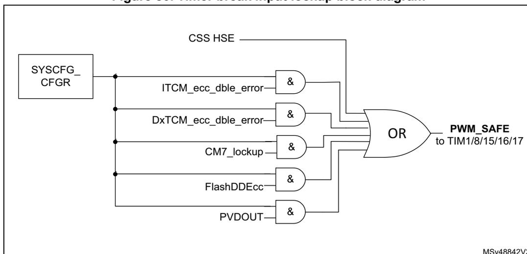
The diagram illustrates the logic for the timer break input lockup. A SYSCFG_CFGR register is connected to five AND gates. The inputs to these AND gates are: ITCM_ecc_dble_error, DxTCM_ecc_dble_error, CM7_lockup, FlashDDEcc, and PVDOUT. The outputs of these AND gates are connected to a single OR gate. The CSS HSE signal is also connected to this OR gate. The output of the OR gate is labeled PWM_SAFE to TIM1/8/15/16/17. The diagram is labeled MSv48842V3.
12.3.4 Management of external interrupt line connections to GPIOs
Any GPIO can be configured as an external interrupt by programming the SYSCFG_EXTICRx registers (refer also to Section 11.3.8: External interrupt/wake-up lines ).
12.3.5 I/O speed in low-voltage mode
The speed of some I/Os can be increased at low voltage by programming the corresponding HSLVx bits in the SYSCFG_CCCSR register. This feature is intended mainly for SDMMC, FMC and OCTOSPI interfaces.
Caution: This feature must be used only when the I/O power supply is below 2.7 V.
12.3.6 I/O compensation cell management
The cell generates an 8-bit value for the I/O buffer (4-bit for N-MOS and 4-bit for P-MOS) that depends on PVT operating conditions (process, voltage, temperature). These bits are used to control the current slew-rate and output impedance in the I/O buffer.
By default, the compensation cell is disabled, and a fixed code is applied to all the I/Os.
When enabled, the compensation cell tracks the PVT, and the 8-bit code (PCV and NCV) is applied to all I/Os for both VDD and VDDMMC I/O supply domains.
To optimize trimming, the code can be adjusted through SYSCFG_CCCR register. Two sets of bitfields are available: PCC/NCC for the VDD power rail and PCC_MMC/NCC_MMC for the VDDMMC power rail. They can be selected independently through CS and CS_MMC bits of SYSCFG_CCCSR register (see Figure 81 ).
When the two power rails are not at the same voltage, it is recommended to adjust VDDMMC code through SYSCFG_CCCR compensation cell code register since the compensation cell tracks the PVT on VDD power supply.
Figure 81. I/O compensation cell block diagram
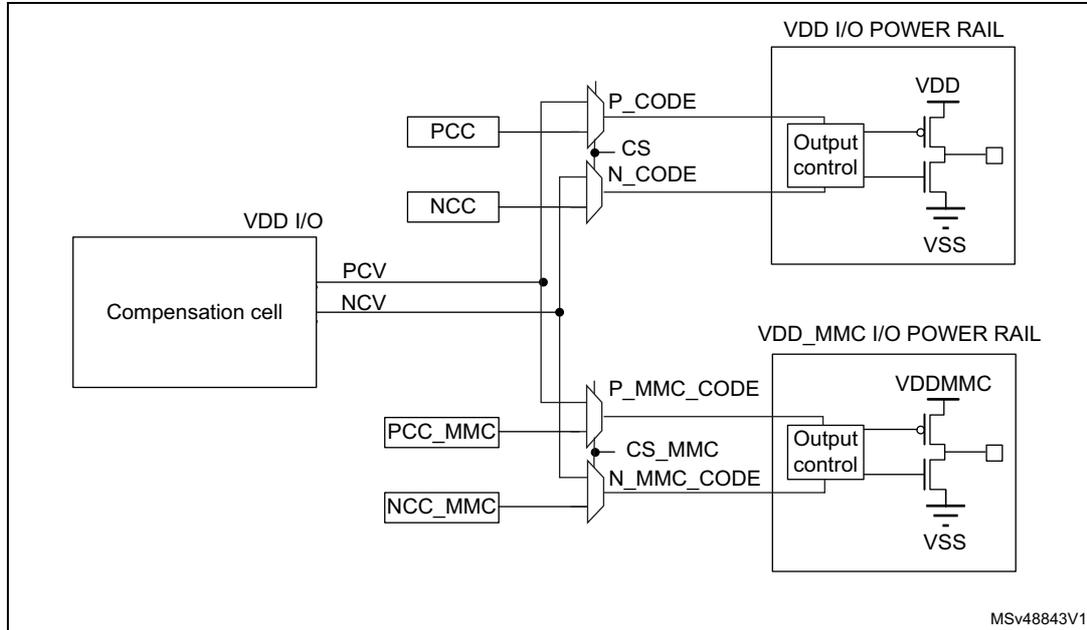
The diagram illustrates the internal structure of the I/O compensation cell. On the left, a 'Compensation cell' block is connected to 'VDD I/O' and provides two output signals, 'PCV' and 'NCV'. These signals are connected to two sets of multiplexers. The top set selects between 'PCC' and 'NCC' inputs, controlled by 'CS', to produce 'P_CODE' and 'N_CODE'. The bottom set selects between 'PCC_MMC' and 'NCC_MMC' inputs, controlled by 'CS_MMC', to produce 'P_MMC_CODE' and 'N_MMC_CODE'. Both sets of codes are fed into 'Output control' blocks. The top 'Output control' block is connected to the 'VDD I/O POWER RAIL' (VDD/VSS). The bottom 'Output control' block is connected to the 'VDD_MMC I/O POWER RAIL' (VDDMMC/VSS). The diagram is labeled 'MSv48843V1' in the bottom right corner.
12.4 SYSCFG registers
12.4.1 SYSCFG peripheral mode configuration register (SYSCFG_PMCR)
Address offset: 0x04
Reset value: 0x0F00 0000
| 31 | 30 | 29 | 28 | 27 | 26 | 25 | 24 | 23 | 22 | 21 | 20 | 19 | 18 | 17 | 16 |
|---|---|---|---|---|---|---|---|---|---|---|---|---|---|---|---|
| Res. | Res. | Res. | Res. | PC3SO | PC2SO | PA1SO | PA0SO | Res. | Res. | Res. | Res. | Res. | Res. | Res. | Res. |
| rw | rw | rw | rw | ||||||||||||
| 15 | 14 | 13 | 12 | 11 | 10 | 9 | 8 | 7 | 6 | 5 | 4 | 3 | 2 | 1 | 0 |
| Res. | Res. | Res. | Res. | Res. | Res. | Res. | Res. | PB9FM P | PB8FM P | PB7FM P | PB6FM P | I2C4F MP | I2C3F MP | I2C2F MP | I2C1F MP |
| rw | rw | rw | rw | rw | rw | rw | rw |
Bits 31:28 Reserved, must be kept at reset value.
Bit 27 PC3SO : PC3 switch open
This bit controls the analog switch between PC3 and PC3_C (dual pad).
0: Analog switch closed (pads connected through the analog switch)
1: Analog switch open (two separated pads)
Bit 26 PC2SO : PC2 switch open
This bit controls the analog switch between PC2 and PC2_C (dual pad).
0: Analog switch closed (pads connected through the analog switch)
1: Analog switch open (two separated pads)
Bit 25 PA1SO : PA1 switch open
This bit controls the analog switch between PA1 and PA1_C (dual pad).
0: Analog switch closed (pads connected through the analog switch)
1: Analog switch open (two separated pads)
Bit 24 PA0SO : PA0 switch open
This bit controls the analog switch between PA0 and PA0_C (dual pad).
0: Analog switch closed (pads connected through the analog switch)
1: Analog switch open (two separated pads)
Bits 23:8 Reserved, must be kept at reset value.
Bit 7 PB9FMP : Fast-mode Plus driving capability activation on PB9
This bit enables the Fm+ driving mode on PB9.
0: PB9 pin operates in standard mode
1: Fm+ mode is enabled on PB9 pin and the speed control is bypassed
Bit 6 PB8FMP : Fast-mode Plus driving capability activation on PB8
This bit enables the Fm+ driving mode on PB8.
0: PB8 pin operates in standard mode
1: Fm+ mode is enabled on PB8 pin and the speed control is bypassed
Bit 5 PB7FMP : Fast-mode Plus driving capability activation on PB7
This bit enables the Fm+ driving mode for PB7.
0: PB7 pin operates in standard mode
1: Fm+ mode is enabled on PB7 pin and the speed control is bypassed
Bit 4 PB6FMP : Fast-mode Plus driving capability activation on PB6
This bit enables the Fm+ driving mode for PB6.
0: PB6 pin operates in standard mode
1: Fm+ mode is enabled on PB6 pin and the speed control is bypassed
Bit 3 I2C4FMP : I2C4 Fm+
This bit enables Fm+ on I2C4.
The corresponding GPIOs are configured in Fast-mode Plus driving capability.
0: Fm+ disabled
1: Fm+ enabled
Bit 2 I2C3FMP : I2C3 Fm+This bit enables Fm+ on I2C3.
The corresponding GPIOs are configured in Fast-mode Plus driving capability
0: Fm+ disabled
1: Fm+ enabled
Bit 1 I2C2FMP : I2C2 Fm+This bit enables Fm+ on I2C2.
The corresponding GPIOs are configured in Fast-mode Plus driving capability
0: Fm+ disabled
1: Fm+ enabled
Bit 0 I2C1FMP : I2C1 Fm+This bit enables Fm+ on I2C1.
The corresponding GPIOs are configured in Fast-mode Plus driving capability
0: Fm+ disabled
1: Fm+ enabled
12.4.2 SYSCFG external interrupt configuration register 1 (SYSCFG_EXTICR1)
Address offset: 0x08
Reset value: 0x0000 0000
| 31 | 30 | 29 | 28 | 27 | 26 | 25 | 24 | 23 | 22 | 21 | 20 | 19 | 18 | 17 | 16 |
|---|---|---|---|---|---|---|---|---|---|---|---|---|---|---|---|
| Res. | Res. | Res. | Res. | Res. | Res. | Res. | Res. | Res. | Res. | Res. | Res. | Res. | Res. | Res. | Res. |
| 15 | 14 | 13 | 12 | 11 | 10 | 9 | 8 | 7 | 6 | 5 | 4 | 3 | 2 | 1 | 0 |
| EXTI3[3:0] | EXTI2[3:0] | EXTI1[3:0] | EXTI0[3:0] | ||||||||||||
| rw | rw | rw | rw | rw | rw | rw | rw | rw | rw | rw | rw | rw | rw | rw | rw |
Bits 31:16 Reserved, must be kept at reset value.
Bits 15:0 EXTIx[3:0] : EXTI x configuration (x = 0 to 3)
These bits are written by software to select the source input for the EXTI input for external interrupt / event detection.
0000: PA[x] pin
0001: PB[x] pin
0010: PC[x] pin
0011: PD[x] pin
0100: PE[x] pin
0101: PF[x] pin
0110: PG[x] pin
0111: PH[x] pin
1000: PI[x] pin
1001: PJ[x] pin
1010: PK[x] pin
Other configurations: reserved
12.4.3 SYSCFG external interrupt configuration register 2 (SYSCFG_EXTICR2)
Address offset: 0x0C
Reset value: 0x0000 0000
| 31 | 30 | 29 | 28 | 27 | 26 | 25 | 24 | 23 | 22 | 21 | 20 | 19 | 18 | 17 | 16 |
|---|---|---|---|---|---|---|---|---|---|---|---|---|---|---|---|
| Res. | Res. | Res. | Res. | Res. | Res. | Res. | Res. | Res. | Res. | Res. | Res. | Res. | Res. | Res. | Res. |
| 15 | 14 | 13 | 12 | 11 | 10 | 9 | 8 | 7 | 6 | 5 | 4 | 3 | 2 | 1 | 0 |
| EXTI7[3:0] | EXTI6[3:0] | EXTI5[3:0] | EXTI4[3:0] | ||||||||||||
| rw | rw | rw | rw | rw | rw | rw | rw | rw | rw | rw | rw | rw | rw | rw | rw |
Bits 31:16 Reserved, must be kept at reset value.
Bits 15:0 EXTIx[3:0] : EXTI x configuration (x = 4 to 7)
These bits are written by software to select the source input for the EXTI input for external interrupt / event detection.
- 0000: PA[x] pin
- 0001: PB[x] pin
- 0010: PC[x] pin
- 0011: PD[x] pin
- 0100: PE[x] pin
- 0101: PF[x] pin
- 0110: PG[x] pin
- 0111: PH[x] pin
- 1000: PI[x] pin
- 1001: PJ[x] pin
- 1010: PK[x] pin
- Other configurations: reserved
12.4.4 SYSCFG external interrupt configuration register 3 (SYSCFG_EXTICR3)
Address offset: 0x10
Reset value: 0x0000 0000
| 31 | 30 | 29 | 28 | 27 | 26 | 25 | 24 | 23 | 22 | 21 | 20 | 19 | 18 | 17 | 16 |
|---|---|---|---|---|---|---|---|---|---|---|---|---|---|---|---|
| Res. | Res. | Res. | Res. | Res. | Res. | Res. | Res. | Res. | Res. | Res. | Res. | Res. | Res. | Res. | Res. |
| 15 | 14 | 13 | 12 | 11 | 10 | 9 | 8 | 7 | 6 | 5 | 4 | 3 | 2 | 1 | 0 |
| EXTI11[3:0] | EXTI10[3:0] | EXTI9[3:0] | EXTI8[3:0] | ||||||||||||
| rw | rw | rw | rw | rw | rw | rw | rw | rw | rw | rw | rw | rw | rw | rw | rw |
Bits 31:16 Reserved, must be kept at reset value.
Bits 15:0 EXTIx[3:0] : EXTI x configuration (x = 8 to 11)
These bits are written by software to select the source input for the AEIC input for external interrupt / event detection.
0000: PA[x] pin
0001: PB[x] pin
0010: PC[x] pin
0011: PD[x] pin
0100: PE[x] pin
0101: PF[x] pin
0110: PG[x] pin
0111: PH[x] pin
1000: PI[x] pin
1001: PJ[x] pin
1010: PK[x] pin
Other configurations: reserved
Note: PK[11:8] are not used.
12.4.5 SYSCFG external interrupt configuration register 4 (SYSCFG_EXTICR4)
Address offset: 0x14
Reset value: 0x0000 0000
| 31 | 30 | 29 | 28 | 27 | 26 | 25 | 24 | 23 | 22 | 21 | 20 | 19 | 18 | 17 | 16 |
|---|---|---|---|---|---|---|---|---|---|---|---|---|---|---|---|
| Res. | Res. | Res. | Res. | Res. | Res. | Res. | Res. | Res. | Res. | Res. | Res. | Res. | Res. | Res. | Res. |
| 15 | 14 | 13 | 12 | 11 | 10 | 9 | 8 | 7 | 6 | 5 | 4 | 3 | 2 | 1 | 0 |
| EXTI15[3:0] | EXTI14[3:0] | EXTI13[3:0] | EXTI12[3:0] | ||||||||||||
| rw | rw | rw | rw | rw | rw | rw | rw | rw | rw | rw | rw | rw | rw | rw | rw |
Bits 31:16 Reserved, must be kept at reset value.
Bits 15:0 EXTIx[3:0] : EXTI x configuration (x = 12 to 15)
These bits are written by software to select the source input for the AEIC input for external interrupt / event detection.
0000: PA[x] pin
0001: PB[x] pin
0010: PC[x] pin
0011: PD[x] pin
0100: PE[x] pin
0101: PF[x] pin
0110: PG[x] pin
0111: PH[x] pin
1001: PJ[x] pin
1010: PK[x] pin
Other configurations: reserved
Note: PK[15:12] are not used.
12.4.6 SYSCFG timer break lockup register (SYSCFG_CFGR)
Address offset: 0x18
Reset value: 0x0000
| 15 | 14 | 13 | 12 | 11 | 10 | 9 | 8 | 7 | 6 | 5 | 4 | 3 | 2 | 1 | 0 |
|---|---|---|---|---|---|---|---|---|---|---|---|---|---|---|---|
| Res. | ITCML | DTCML | Res. | Res. | Res. | Res. | Res. | Res. | CM7L | Res. | Res. | FLASHL | PVDL | Res. | Res. |
| rs | rs | rs | rs | rs |
Bit 15 Reserved, must be kept at reset value.
Bit 14 ITCML : ITCM double ECC error signal lock
This bit is set by software and cleared only by a reset system.
It is used to enable and lock the ITCM double ECC error signal connection to TIM1/8/15/16 /17 Break inputs.
0: ITCM double ECC disconnected
1: ITCM double ECC connected
Bit 13 DTCML : D1TCM or D0TCM double ECC error signal lock
This bit is set by software and cleared only by reset system.
It is used to enable and lock the DxTCM double ECC error signal connection to TIM1/8/15/16 /17 Break inputs.
0: DxTCM double ECC disconnected
1: DxTCM double ECC connected
Bits 12:7 Reserved, must be kept at reset value.
Bit 6 CM7L : Cortex ® -M7 LOCKUP (HardFault) output enable bit
This bit is set by software and cleared only by reset system.
It is used to enable and lock the Cortex ® -M7 LOCKUP output connection to TIM1/8/15/16 /17 Break inputs.
0: Cortex ® -M7 LOCKUP output disconnected
1: Cortex ® -M7 LOCKUP output connected
Bits 5:4 Reserved, must be kept at reset value.
Bit 3 FLASHL : Flash double ECC error lock bit
This bit is set by software and cleared only by reset system.
It is used to enable and lock the Cortex ® -M7 LOCKUP output connection to TIM1/8/15/16 /17 Break inputs.
0: Double ECC disconnected
1: Double ECC connected
Bit 2 PVDL : PVD lock enable bit.
This bit is set by software and cleared only by reset system.
It is used to enable and lock the PVD connection to TIM1/8/15/16 /17 Break inputs.
0: PVD signal disconnected
1: PVD signal connected
Bits 1:0 Reserved, must be kept at reset value.
12.4.7 SYSCFG compensation cell control/status register (SYSCFG_CCCSR)
Address offset: 0x20
Reset value: 0x0000 0000
Refer to Section 11.3.11: I/O compensation cell for a detailed description of I/O compensation mechanism.
| 31 | 30 | 29 | 28 | 27 | 26 | 25 | 24 | 23 | 22 | 21 | 20 | 19 | 18 | 17 | 16 |
|---|---|---|---|---|---|---|---|---|---|---|---|---|---|---|---|
| Res. | Res. | Res. | Res. | Res. | Res. | Res. | Res. | Res. | Res. | Res. | Res. | HSLV3 | HSLV2 | HSLV1 | HSLV0 |
| rw | rw | rw | rw | ||||||||||||
| 15 | 14 | 13 | 12 | 11 | 10 | 9 | 8 | 7 | 6 | 5 | 4 | 3 | 2 | 1 | 0 |
| Res. | Res. | Res. | Res. | Res. | Res. | Res. | READY | Res. | Res. | Res. | Res. | CS_MMC | Res. | CS | EN |
| r | rw | rw | rw |
Bits 31:17 Reserved , must be kept at reset value.
Bit 19 HSLV3: High-speed at low-voltage for VDDMMC I/Os
This bit is written by software to optimize the I/O speed when the product voltage is low.
It is active only if VDDMMC_HSLV user option bit is set. It must be used only when the VDDMMC I/O power supply is below 2.7 V. Setting this bit when
\(
V_{DDMMC}
\)
is higher than 2.7 V might damage the I/Os.
It controls the speed of the following I/Os (mainly SDIO on VDDMMC power rail): PB[9:8], PD[7:6] and PG[14:9].
0: No I/O speed optimization
1: I/O speed optimization
Bit 18 HSLV2: High-speed at low-voltage for VDD I/Os
This bit is written by software to optimize the I/O speed when the product voltage is low.
It is active only if VDDIO_HSLV user option bit is set. It must be used only when the VDD I/O power supply is below 2.7 V. Setting this bit when
\(
V_{DD}
\)
is higher than 2.7 V might damage the I/Os.
This bit controls the speed of the following I/Os (mainly for FMC): PD[15:8], PD[3], PD[1:0], PE[15:0], PF[15:12], PF[5:2], PG[8:0], PH[15:8], PH[3:2], PI[10:9] and PI[7:0].
0: No I/O speed optimization
1: I/O speed optimization
Bit 17 HSLV1: High-speed at low-voltage for VDD I/Os
This bit is written by software to optimize the I/O speed when the product voltage is low.
It is active only if VDDIO_HSLV user option bit is set. It must be used only when the VDD I/O power supply is below 2.7 V. Setting this bit when
\(
V_{DD}
\)
is higher than 2.7 V might damage the I/Os.
It control the speed of the following I/Os (mainly for OCTOSPI): PA[7:6], PA[3], PA[1], PB[12], PB[2], PC[5], PD[5:4], PF[11:6], PG[15], PI[4:2], PJ[2:1] and PK[6:3].
0: No I/O speed optimization
1: I/O speed optimization
Bit 16 HSLV0 : High-speed at low-voltage for VDD I/Os
This bit is written by software to optimize the I/O speed when the product voltage is low.
It is active only if VDDIO_HSLV user option bit is set. It must be used only when the VDD I/O power supply is below 2.7 V. Setting this bit when \( V_{DD} \) is higher than 2.7 V might damage the I/Os.
This bit controls the speed of the following I/Os (mainly for SDMMC or others): PA[8], PA[5], PB[15:13], PB[5:3], PB[1:0], PC[12:6], PC[1] and PD[2].
0: No I/O speed optimization
1: I/O speed optimization
Bits 15:9 Reserved, must be kept at reset value.
Bit 8 READY : Compensation cell ready flag
This bit provides the status of the compensation cell.
0: I/O compensation cell not ready
1: I/O compensation cell ready
Bits 7:4 Reserved, must be kept at reset value.
Bit 3 CS_MMC : Code selection for VDDMMC power rail
This bit selects the code to be applied to the VDDMMC I/O buffer.
0: Value from the compensation cell (available in the SYSCFG_CCVR)
1: Code register from the SYSCFG compensation cell code bits (available in SYSCFG_CCCR)
Bit 2 Reserved, must be kept at reset value.
Bit 1 CS : Code selection for all VDD power rails
This bit selects the code to be applied to the VDD I/O buffer.
0: Value from the compensation cell (available in the SYSCFG_CCVR)
1: Code register from the SYSCFG compensation cell code (available in SYSCFG_CCCR)
Bit 0 EN : Enable bit
This bit enables the I/O compensation cell.
0: I/O compensation cell disabled
1: I/O compensation cell enabled
12.4.8 SYSCFG compensation cell value register (SYSCFG_CCVR)
Address offset: 0x24
Reset value: 0x0000 0088
| 31 | 30 | 29 | 28 | 27 | 26 | 25 | 24 | 23 | 22 | 21 | 20 | 19 | 18 | 17 | 16 |
|---|---|---|---|---|---|---|---|---|---|---|---|---|---|---|---|
| Res. | Res. | Res. | Res. | Res. | Res. | Res. | Res. | Res. | Res. | Res. | Res. | Res. | Res. | Res. | Res. |
| 15 | 14 | 13 | 12 | 11 | 10 | 9 | 8 | 7 | 6 | 5 | 4 | 3 | 2 | 1 | 0 |
| Res. | Res. | Res. | Res. | Res. | Res. | Res. | Res. | PCV[3:0] | NCV[3:0] | ||||||
| r | r | r | r | r | r | r | r | ||||||||
Bits 31:8 Reserved, must be kept at reset value.
Bits 7:4 PCV[3:0] : PMOS compensation cell value
This value is provided by the cell and can be used by the CPU to compute an I/O compensation cell code for PMOS transistors. This code is applied to the I/O compensation cell when the CS bit of the SYSCFG_CCCSR is reset.
Bits 3:0 NCV[3:0] : NMOS compensation cell value
This value is provided by the cell and can be used by the CPU to compute an I/O compensation cell code for NMOS transistors. This code is applied to the I/O compensation cell when the CS bit of the SYSCFG_CCCSR is reset.
12.4.9 SYSCFG compensation cell code register (SYSCFG_CCCR)
Address offset: 0x28
Reset value: 0x0000 0000
| 31 | 30 | 29 | 28 | 27 | 26 | 25 | 24 | 23 | 22 | 21 | 20 | 19 | 18 | 17 | 16 |
|---|---|---|---|---|---|---|---|---|---|---|---|---|---|---|---|
| Res. | Res. | Res. | Res. | Res. | Res. | Res. | Res. | Res. | Res. | Res. | Res. | Res. | Res. | Res. | Res. |
| 15 14 13 12 | 11 10 9 8 | 7 6 5 4 | 3 2 1 0 | ||||||||||||
| PCC_MMC[3:0] | NCC_MMC[3:0] | PCC[3:0] | NCC[3:0] | ||||||||||||
| rw | rw | rw | rw | rw | rw | rw | rw | rw | rw | rw | rw | rw | rw | rw | rw |
Bits 31:16 Reserved, must be kept at reset value.
Bits 15:12 PCC_MMC[3:0] : PMOS compensation code register
These bits are written by software to define an I/O compensation cell code for PMOS transistors corresponding to the VDDMMC power rail.
This code is applied to the I/O when the CS_MMC bit of SYSCFG_CCCSR is set.
Bits 11:8 NCC_MMC[3:0] : NMOS compensation code register
These bits are written by software to define an I/O compensation cell code for NMOS transistors corresponding to the VDDMMC power rail.
This code is applied to the I/O when the CS_MMC bit of SYSCFG_CCCSR is set.
Bits 7:4 PCC[3:0] : PMOS compensation code register
These bits are written by software to define an I/O compensation cell code for PMOS transistors corresponding to the VDD power rail.
This code is applied to the I/O when the CS bit of SYSCFG_CCCSR is set.
Bits 3:0 NCC[3:0] : NMOS compensation code register
These bits are written by software to define an I/O compensation cell code for NMOS transistors corresponding to the VDD power rail.
This code is applied to the I/O when the CS bit of SYSCFG_CCCSR is set.
12.4.10 SYSCFG register maps
The following table gives the SYSCFG register map and the reset values.
Table 75. SYSCFG register map and reset values
| Offset | Register | 31 | 30 | 29 | 28 | 27 | 26 | 25 | 24 | 23 | 22 | 21 | 20 | 19 | 18 | 17 | 16 | 15 | 14 | 13 | 12 | 11 | 10 | 9 | 8 | 7 | 6 | 5 | 4 | 3 | 2 | 1 | 0 |
|---|---|---|---|---|---|---|---|---|---|---|---|---|---|---|---|---|---|---|---|---|---|---|---|---|---|---|---|---|---|---|---|---|---|
| 0x00 | Reserved | Reserved | |||||||||||||||||||||||||||||||
| 0x04 | SYSCFG_PMC | Res. | Res. | Res. | Res. | PC3SO | PC2SO | PA1SO | PA0SO | Res. | Res. | Res. | Res. | Res. | Res. | Res. | Res. | Res. | Res. | Res. | Res. | Res. | Res. | Res. | Res. | PB9FMP | PB8FMP | PB7FMP | PB6FMP | I2C4FMP | I2C3FMP | I2C2FMP | I2C1FMP |
| Reset value | 1 | 1 | 1 | 1 | 0 | 0 | 0 | 0 | 0 | 0 | 0 | 0 | |||||||||||||||||||||
| 0x08 | SYSCFG_EXTICR1 | Res. | Res. | Res. | Res. | Res. | Res. | Res. | Res. | Res. | Res. | Res. | Res. | Res. | Res. | Res. | Res. | EXTI3[3:0] | EXTI2[3:0] | EXTI1[3:0] | EXTI0[3:0] | ||||||||||||
| Reset value | 0 0 0 0 | 0 0 0 0 | 0 0 0 0 | 0 0 0 0 | |||||||||||||||||||||||||||||
| 0x0C | SYSCFG_EXTICR2 | Res. | Res. | Res. | Res. | Res. | Res. | Res. | Res. | Res. | Res. | Res. | Res. | Res. | Res. | Res. | Res. | EXTI7[3:0] | EXTI6[3:0] | EXTI5[3:0] | EXTI4[3:0] | ||||||||||||
| Reset value | 0 0 0 0 | 0 0 0 0 | 0 0 0 0 | 0 0 0 0 | |||||||||||||||||||||||||||||
| 0x10 | SYSCFG_EXTICR3 | Res. | Res. | Res. | Res. | Res. | Res. | Res. | Res. | Res. | Res. | Res. | Res. | Res. | Res. | Res. | Res. | EXTI11[3:0] | EXTI10[3:0] | EXTI9[3:0] | EXTI8[3:0] | ||||||||||||
| Reset value | 0 0 0 0 | 0 0 0 0 | 0 0 0 0 | 0 0 0 0 | |||||||||||||||||||||||||||||
| 0x14 | SYSCFG_EXTICR4 | Res. | Res. | Res. | Res. | Res. | Res. | Res. | Res. | Res. | Res. | Res. | Res. | Res. | Res. | Res. | Res. | EXTI15[3:0] | EXTI14[3:0] | EXTI13[3:0] | EXTI12[3:0] | ||||||||||||
| Reset value | 0 0 0 0 | 0 0 0 0 | 0 0 0 0 | 0 0 0 0 | |||||||||||||||||||||||||||||
| 0x18 | SYSCFG_CFGR | Res. | Res. | Res. | Res. | Res. | Res. | Res. | Res. | Res. | Res. | Res. | Res. | Res. | Res. | Res. | Res. | ITCML | DTCML | Res. | Res. | Res. | Res. | Res. | Res. | CM7L | Res. | Res. | FLASH | PVDL | Res. | Res. | |
| Reset value | 0 | 0 | 0 | 0 | 0 | ||||||||||||||||||||||||||||
| 0x20 | SYSCFG_CCCS_R | Res. | Res. | Res. | Res. | Res. | Res. | Res. | Res. | Res. | Res. | Res. | Res. | HSLV[3:0] | Res. | Res. | Res. | Res. | Res. | Res. | Res. | READY | Res. | Res. | Res. | Res. | Res. | Res. | CS_MMC | Res. | CS | EN | |
| Reset value | 0 0 0 0 | 0 | 0 | 0 | 0 | 0 | |||||||||||||||||||||||||||
| 0x24 | SYSCFG_CCVR | Res. | Res. | Res. | Res. | Res. | Res. | Res. | Res. | Res. | Res. | Res. | Res. | Res. | Res. | Res. | Res. | Res. | Res. | Res. | Res. | PCV[3:0] | NCV[3:0] | ||||||||||
| Reset value | 1 0 0 0 | 1 0 0 0 | |||||||||||||||||||||||||||||||
| 0x28 | SYSCFG_CCCR | Res. | Res. | Res. | Res. | Res. | Res. | Res. | Res. | Res. | Res. | Res. | Res. | Res. | Res. | Res. | Res. | PCC_MMC[3:0] | NCC_MMC[3:0] | PCC[3:0] | NCC[3:0] | ||||||||||||
| Reset value | 0 0 0 0 | 0 0 0 0 | 0 0 0 0 | 0 0 0 0 | |||||||||||||||||||||||||||||
Refer to Section 2.3 on page 131 for the register boundary addresses.