8. Reset and clock control (RCC)
The RCC block manages the clock and reset generation for the whole microcontroller.
The RCC block is located in the SmartRun domain (refer to Section 6: Power control (PWR) for a detailed description).
The operating modes this section refers to are defined in Section 6.6.1: System operating modes of the PWR block.
8.1 RCC main features
Reset block
- • Generation of local and system reset
- • Bidirectional pin reset allowing to reset the microcontroller or external devices
- • WWDG and IWDG reset supported
- • Power-on (POR) and Brownout (BOR) resets initiated by the power control (PWR)
Clock generation block
- • Generation and dispatching of clocks for the complete device
- • 3 separate PLLs using integer or fractional ratios
- • Possibility to change the PLL fractional ratios on-the-fly
- • Smart clock gating to reduce power dissipation
- • 2 external oscillators:
- – High-speed external oscillator (HSE) supporting a wide range of crystals from 4 to 50 MHz frequency
- – Low-speed external oscillator (LSE) for the 32 kHz crystals
- • 4 internal oscillators
- – High-speed internal oscillator (HSI)
- – 48 MHz RC oscillator (HSI48)
- – Low-power internal oscillator (CSI)
- – Low-speed internal oscillator (LSI)
- • Buffered clock outputs for external devices
- • Generation of two types of interrupts lines:
- – Dedicated interrupt lines for clock security management
- – One general interrupt line for other events
- • Clock generation handling in Stop and Standby mode
- • SmartRun domain Autonomous mode
8.2 RCC block diagram
Figure 44 shows the RCC block diagram.
Figure 44. RCC block diagram
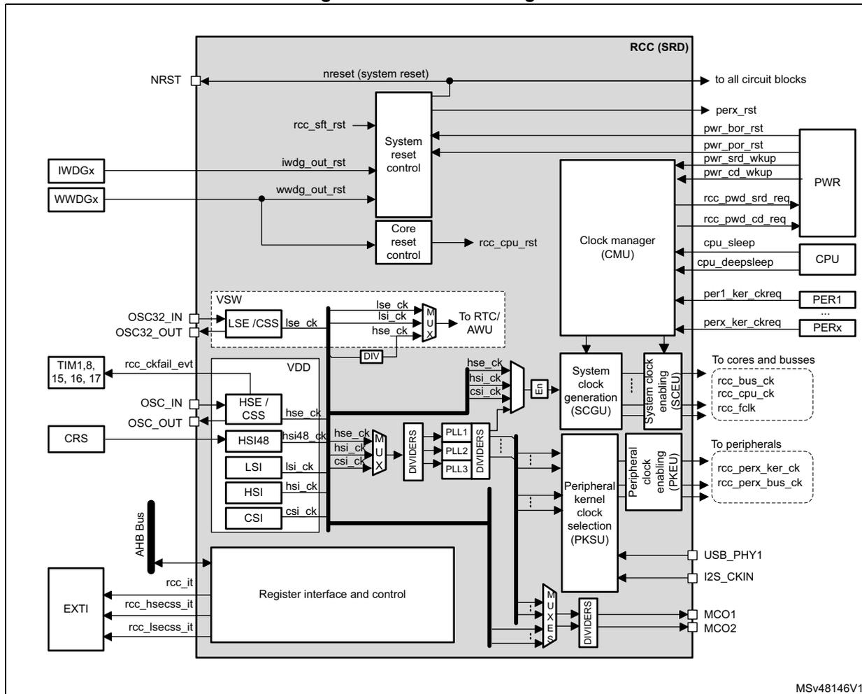
The diagram illustrates the internal architecture of the RCC (SRD). At the top, the NRST pin is connected to a 'nreset (system reset)' signal that goes to all circuit blocks. Below this, the 'System reset control' block receives inputs from IWDGx, WWDGx, and 'rcc_sft_rst', and outputs 'rcc_cpu_rst'. The 'Core reset control' block also receives inputs from IWDGx, WWDGx, and 'rcc_sft_rst', and outputs 'rcc_cpu_rst'. The 'Clock manager (CMU)' block is connected to the 'System clock generation (SCGU)' and 'Peripheral kernel clock selection (PKSU)' blocks. The 'SCGU' block receives inputs from various oscillators (LSE/CSS, HSE/CSS, HSI48, LSI, HSI, CSI) and PLLs (PLL1, PLL2, PLL3). The 'PKSU' block receives inputs from the 'SCGU' and 'Peripheral clock enabling (PKEU)' blocks. The 'PKEU' block is connected to the 'USB_PHY1', 'I2S_CKIN', 'MCO1', and 'MCO2' pins. The 'Register interface and control' block is connected to the 'AHB Bus' and provides control signals for the RCC. External connections include NRST, OSC32_IN, OSC32_OUT, OSC_IN, CRS, TIM1,8,15,16,17, and EXTI.
8.3 RCC pins and internal signals
Table 51 lists the RCC inputs and output signals connected to package pins or balls.
Table 51. RCC input/output signals connected to package pins or balls
| Signal name | Signal type | Description |
|---|---|---|
| NRST | I/O | System reset, can be used to provide reset to external devices |
| OSC32_IN | I | 32 kHz oscillator input |
| OSC32_OUT | O | 32 kHz oscillator output |
| OSC_IN | I | System oscillator input |
| Signal name | Signal type | Description |
|---|---|---|
| OSC_OUT | O | System oscillator output |
| MCO1 | O | Output clock 1 for external devices |
| MCO2 | O | Output clock 2 for external devices |
| I2S_CKIN | I | External kernel clock input for digital audio interfaces: SPI/I2S, SAI, and DFSDM |
| USB_PHY1 | I | USB clock input provided by the external USB_PHY |
The RCC exchanges a lot of internal signals with all components of the product, for that reason, Table 52 only shows the most significant internal signals.
Table 52. RCC internal input/output signals| New signal name | Signal type | Description |
|---|---|---|
| rcc_it | O | General interrupt request line |
| rcc_hsecss_it | O | HSE clock security failure interrupt |
| rcc_lsecss_it | O | LSE clock security failure interrupt |
| rcc_ckfail_evt | O | Event indicating that a HSE clock security failure is detected. This signal is connected to TIMERS. |
| nreset | I/O | System reset |
| iwdg_out_rst | I | Reset line driven by the IWDG, indicating that a timeout occurred |
| wwdg_out_rst | I | Reset line driven by the WWDG, indicating that a timeout occurred |
| pwr_bor_rst | I | Brownout reset generated by the PWR block |
| pwr_por_rst | I | Power-on reset generated by the PWR block |
| pwr_vsw_rst | I | Power-on reset of the VSW domain generated by the PWR block |
| rcc_perx_rst | O | Reset generated by the RCC for the peripherals |
| pwr_cd_wkup | I | Wake-up domain request generated by the PWR and used to restore the domain clocks |
| pwr_srd_wkup | I | Wake-up domain request generated by the PWR and used to restore the domain clocks |
| rcc_pwd_cd_req | O | Low-power request generated by the RCC and used to set the domain into low-power mode |
| rcc_pwd_srd_req | O | Low-power request generated by the RCC and used to set the domain into low-power mode |
| cpu_sleep | I | Signals generated by the CPU, indicating if the CPU is in CRun, CSleep or CStop |
| cpu_deepsleep | I | |
| perx_ker_ckreq | I | Signal generated by some peripherals in order to request the activation of their kernel clock |
| rcc_perx_ker_ck | O | Kernel clock signals generated by the RCC, for some peripherals |
Table 52. RCC internal input/output signals (continued)
| New signal name | Signal type | Description |
|---|---|---|
| rcc_perx_bus_ck | O | Bus interface clock signals generated by the RCC for peripherals |
| rcc_bus_ck | O | Clocks for APB, AHB and AXI bridges generated by the RCC |
| rcc_cpu_ck | O | Clocks for the CPU, generated by the RCC |
| rcc_fclk_c | O |
8.4 RCC reset block functional description
The following sources can generate a reset:
- • an external device via NRST pin
- • a failure on the supply voltage applied to VDD
- • a watchdog timeout
- • a software command
The reset scope depends on the source that generates the reset.
Three reset categories exist:
- • power-on/off reset
- • system reset
- • local resets
8.4.1 Power-on/off reset
The power-on/off reset ( pwr_por_rst ) is generated by the power controller block (PWR). It is activated when the input voltage ( \( V_{DD} \) ) is below a threshold level. This is the most complete reset since it resets the whole circuit, except the Backup domain.
The power-on/off reset function can be disabled through PDR_ON pin (see Section 6.5: Power supply supervision ).
Refer to Table 53: Reset distribution summary for details.
8.4.2 System reset
A system reset ( nreset ) resets all registers to their default values unless otherwise specified in the register description.
A system reset can be generated from one of the following sources:
- • a reset from NRST pin (external reset)
- • a reset from the power-on/off reset block ( pwr_por_rst )
- • a reset from the brownout reset block (
pwr_bor_rst
)
Refer to Section 6.5.2: Brownout reset (BOR) for a detailed description of the BOR function. - • a reset from the independent watchdogs ( iwdg_out_rst )
- • a software reset from the Cortex
®
-M7 core
It is generated via the SYSRESETREQ signal issued by the Cortex ® -M7 core. This signal is also named SFTRESET in this document. - • a reset from the window watchdogs depending on WWDG configuration ( wwdg_out_rst )
- • A reset from the low-power mode security reset, depending on option byte configuration ( lpwr_rst )
Note: The SYSRESETREQ bit in Cortex ® -M7 through the FPU application interrupt and reset control register, must be set to force a software reset on the device. Refer to the Cortex ® -M7 with FPU technical reference manual for more details (see http://infocenter.arm.com ).
As shown in Figure 45 , some internal sources (such as pwr_por_rst , pwr_bor_rst , iwdg_out_rst ) perform a system reset of the circuit, which is also propagated to the NRST pin to reset the connected external devices. The pulse generator guarantees a minimum reset pulse duration of 20 \( \mu\text{s} \) for each internal reset source. In case of an external reset, the reset pulse is generated while the NRST pin is asserted low.
Note: It is not recommended to let the NRST pin unconnected. When it is not used, connect this pin to ground via a 10 to 100 nF capacitor ( \( C_R \) in Figure 45 ).
Figure 45. System reset circuit
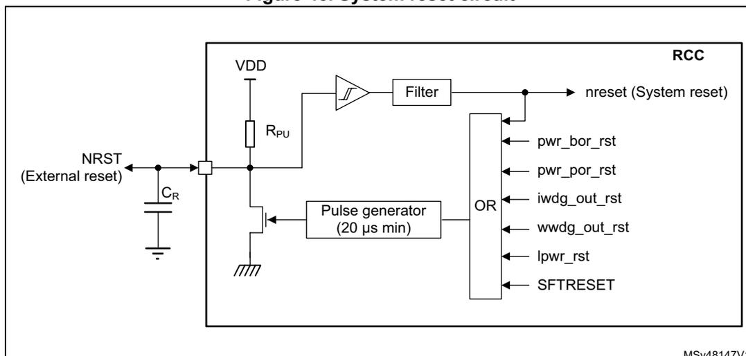
MSV48147V1
8.4.3 Local resets
Domain reset
When the system exits from Standby mode, a stby_rst reset is applied. The stby_rst signal generates a reset of the complete \( V_{CORE} \) domain as long the \( V_{CORE} \) voltage provided by the internal regulator is not valid.
Table 53 gives a detailed overview of reset sources and scopes.
Table 53. Reset distribution summary
| Reset source | Reset name | CPU | CD interconnect | CD peripherals | CD debug | CD WWDG | SRD peripherals | CD IWDG | FLASH | RTC domain | Backup RAM | System supply | NRST pin | Comments |
|---|---|---|---|---|---|---|---|---|---|---|---|---|---|---|
| Pin | NRST | x | x | x | - | x | x | x | - | - | - | - | x |
|
| PWR | pwr_bor_rst | x | x | x | - | x | x | x | - | - | - | - | x | Same as pin reset. The pin is asserted as well. |
| pwr_por_rst | x | x | x | x | x | x | x | x | - | - | x | x |
| |
| lpwr_rst | x | x | x | - | x | x | x | - | - | - | - | x |
| |
| RCC | VSWRST | - | - | - | - | - | - | - | - | x | - | - | - |
|
| stby_rst | x | x | x | x | x | x | - | - | - | - | - | - |
| |
| CPU | SFTRESET | x | x | x | - | x | x | x | - | - | - | - | x |
|
| Backup domain | pwr_vsw_rst | - | - | - | - | - | - | - | - | x | - | - | - |
|
| IWDG | iwdg_out_rst | x | x | x | - | x | x | x | - | - | - | - | x | Same as pwr_bor_rst reset |
| WWDG | wwdg_out_rst | x | x | x | - | x | x | x | - | - | - | - | x | Same as pwr_bor_rst reset |
8.4.4 Reset source identification
The CPU can identify the reset source by checking the reset flags in the RCC_RSR register.
The CPU can reset the flags by setting RMVF bit.
Table 54 shows how the status bits of the RCC_RSR register behave according to the situation that generated the reset. For example, when an IWDG timeout occurs (line #6), if the CPU is reading the RCC_RSR register during the boot phase, both PINRSTF and IWDGRSTF bits are set, indicating that the IWDG also generated a pin reset.
Table 54. Reset source identification (RCC_RSR) (1)
| # | Situations generating a reset | LPWRRSTF | WWDGRSTF | IWDGRSTF | SFTRSTF | PORRSTF | PINRSTF | BORRSTF | CDRSTF |
|---|---|---|---|---|---|---|---|---|---|
| 1 | Power-on reset (pwr_por_rst) | 0 | 0 | 0 | 0 | 1 | 1 | 1 | 1 |
| 2 | Pin reset (NRST) | 0 | 0 | 0 | 0 | 0 | 1 | 0 | 0 |
| 3 | Brownout reset (pwr_bor_rst) | 0 | 0 | 0 | 0 | 0 | 1 | 1 | 0 |
| 4 | System reset generated by CPU (SFTRESET) | 0 | 0 | 0 | 1 | 0 | 1 | 0 | 0 |
| 5 | WWDG reset (wwdg_out_rst) | 0 | 1 | 0 | 0 | 0 | 1 | 0 | 0 |
| 6 | IWDG reset (iwdg_out_rst) | 0 | 0 | 1 | 0 | 0 | 1 | 0 | 0 |
| 7 | CPU domain exits DStop mode and pin reset during DStop | 0 | 0 | 0 | 0 | 0 | 1 | 0 | 0 |
| 8 | CPU domain exits DStop2 mode and pin reset during DStop2 | 0 | 0 | 0 | 0 | 0 | 1 | 0 | 1 |
| 9 | CPU erroneously enters CStop mode | 1 | 0 | 0 | 0 | 0 | 1 | 0 | 0 |
1. Grayed cells highlight the register bits that are set.
8.4.5 Low-power mode security reset (lpwr_rst)
To prevent critical applications from mistakenly enter a low-power mode, two low-power mode security resets are available. When enabled through nRST_STOP_CD and nRST_STANDBY option bytes, a system reset is generated if the following conditions are met:
- • The CPU domain (CD) accidentally enters Dstop or Dstop2 mode.
This type of reset is enabled by resetting nRST_STOP_CD user option byte. In this case, whenever the Dstop or Dstop2 mode entry sequence is successfully executed, a system reset is generated. - • CPU and system accidentally enter Standby mode.
This type of reset is enabled by resetting nRST_Standby user option byte. In this case, whenever a Standby mode entry sequence is successfully executed, a system reset is generated.
When the Standby mode is entered, a flag is also set in the power controller.
LPWRRSTF bit in the RCC reset status register (RCC_RSR) indicates that a low-power mode security reset occurred (see line #9 in Table 54 ).
lpwr_rst is activated when a low-power mode security reset due to CPU occurred.
Refer to Section 4.4: FLASH option bytes for additional information.
Refer to Section 6: Power control (PWR) for additional information and Table 35: Operating mode summary for the overview of the existing power modes
8.4.6 Backup domain reset
A Backup domain reset is generated when one of the following events occurs:
- • A software reset, triggered by setting VSWRST bit in the RCC Backup domain control register (RCC_BDCR) . All RTC registers and the RCC_BDCR register are reset to their default values. The backup RAM is not affected.
- • \( V_{SW} \) voltage is outside the operating range. All RTC registers and the RCC_BDCR register are reset to their default values. In this case the content of the backup RAM is no longer valid.
There are two ways to reset the backup RAM:
- • through the flash memory interface by requesting a protection level change from 1 to 0
- • when a tamper event occurs
Refer to Section 6.4.5: Backup domain section of PWR block for additional information.
8.4.7 Power-on and wake-up sequences
For detailed diagrams refer to Section 6.4.1: System supply startup in the PWR section.
The time interval between the event that exits the product from a low-power and the moment where the CPU is able to execute code, depends on the system state and on its configuration. Figure 46 shows the most usual examples.
Power-on wake-up sequence
The power-on wake-up sequence shown in Figure 46 gives the most significant phases of the power-on sequence. It is the longest sequence since the circuit was not powered. Note that this sequence remains unchanged, whatever \( V_{BAT} \) was present or not.
Boot from pin reset
When a pin reset occurs, \( V_{DD} \) is still present. As a result:
- • The regulator settling time is faster since the reference voltage is already stable.
- • The HSI restart delay may be needed if the HSI was not enabled when the NRST occurred, otherwise this restart delay phase is skipped.
- • The flash memory power recovery delay can also be skipped if the flash memory was enabled when the NRST occurred.
Note: The boot sequence is similar for pwr_bor_rst, lpwr_rst, STFxRESET, iwdg_out_rst and wwdg_out_rst.
Boot from system Standby
When waking up from system Standby, the reference voltage is stable since \( V_{DD} \) has not been removed. As a result, the regulator settling time is fast. Since \( V_{CORE} \) was not present, the restart delay for the HSI, the flash memory power recovery and the option byte reloading cannot be skipped.
Restart from system Stop
When restarting from system Stop (CPU domain can be in DStop or DStop2), \( V_{DD} \) is still present. As a result, the sequence is mainly composed of three steps:
- 1. Regulator settling time to reach VOS3 (default voltage).
- 2. Power switch (ePOD) settling time to change from Retention mode to Normal mode in case of DStop2.
- 3. HSI/CSI restart delay. This step can be skipped if HSIKERON or CSIKERON bit is set to 1 in the RCC source control register (RCC_CR) .
Restart from system Autonomous mode with CPU domain in DStop/DStop2
Since the SRD domain is in Run mode, the regulator is already activated.
The restart sequence of the CPU domain in DStop or Dstop2 mode is mainly composed of two steps:
- 1. Handshake between RCC, EXTI and PWR blocks.
- 2. The power-switch (ePOD) settling time to change from retention mode to normal mode in case of DStop2.
Restart from domain DStop
The restart sequence of a domain from DStop is mainly composed of the handshake between the RCC, EXTI and PWR blocks.
Figure 46. Boot sequences versus system states
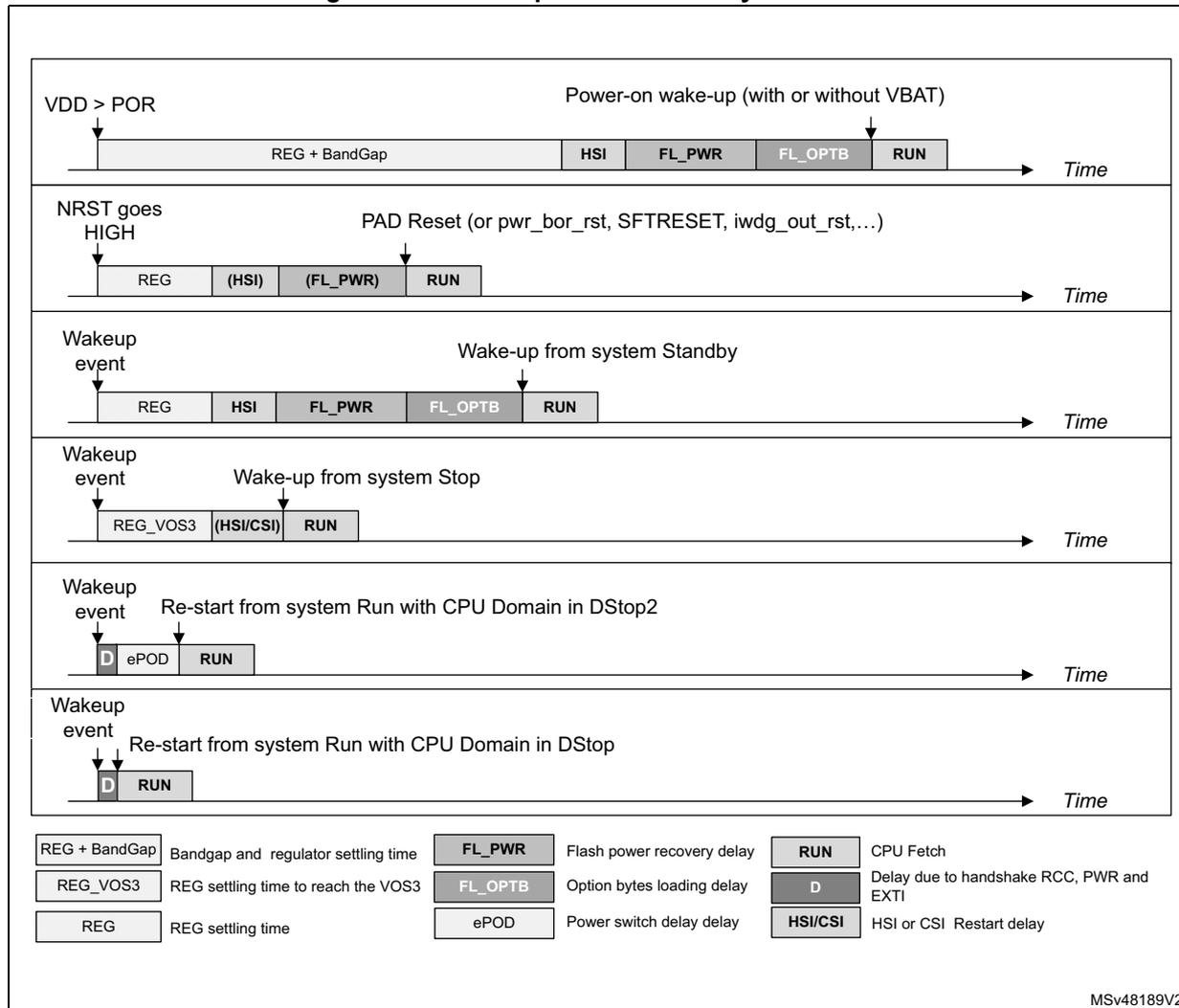
The figure displays six timing diagrams illustrating different boot sequences over time. Each diagram shows the sequence of system states and delays from an initial event to the final 'RUN' state.
- Power-on wake-up (with or without VBAT): Triggered by VDD > POR. Sequence: [REG + BandGap] → [HSI] → [FL_PWR] → [FL_OPTB] → [RUN].
- PAD Reset (or pwr_bor_rst, SFTRESET, iwdg_out_rst,...): Triggered when NRST goes HIGH. Sequence: [REG] → [(HSI)] → [(FL_PWR)] → [RUN].
- Wake-up from system Standby: Triggered by a wakeup event. Sequence: [REG] → [HSI] → [FL_PWR] → [FL_OPTB] → [RUN].
- Wake-up from system Stop: Triggered by a wakeup event. Sequence: [REG_VOS3] → [(HSI/CSI)] → [RUN].
- Re-start from system Run with CPU Domain in DStop2: Triggered by a wakeup event. Sequence: [D] → [ePOD] → [RUN].
- Re-start from system Run with CPU Domain in DStop: Triggered by a wakeup event. Sequence: [D] → [RUN].
Legend:
| [REG + BandGap] | Bandgap and regulator settling time | [FL_PWR] | Flash power recovery delay | [RUN] | CPU Fetch |
| [REG_VOS3] | REG settling time to reach the VOS3 | [FL_OPTB] | Option bytes loading delay | [D] | Delay due to handshake RCC, PWR and EXTI |
| [REG] | REG settling time | [ePOD] | Power switch delay delay | [HSI/CSI] | HSI or CSI Restart delay |
MSV48189V2
8.5 RCC clock block functional description
The RCC provides a wide choice of clock generators:
- • HSI (high-speed internal oscillator) clock: ~ 8, 16, 32 or 64 MHz
- • HSE (high-speed external oscillator) clock: 4 to 48 MHz
- • LSE (low-speed external oscillator) clock: 32 kHz
- • LSI (low-speed internal oscillator) clock: ~ 32 kHz
- • CSI (low-power internal oscillator) clock: ~4 MHz
- • HSI48 (high-speed internal oscillator) clock: ~48 MHz
The RCC offers then a high flexibility for the application to select the appropriate clock for CPU and peripherals, in particular for peripherals that require a specific clock such as USB OTG-FS and HS, SPI/I2S, SAI and SDMMC.
To optimize the power consumption, each clock source can be switched ON or OFF independently.
The RCC provides up to 3 PLLs; each of them can be configured with integer or fractional ratios.
As shown in the Figure 47 , the RCC offers two clock outputs (MCO1 and MCO2), with a great flexibility on the clock selection and frequency adjustment.
The SCGU block (system clock generation unit) contains several prescalers used to configure the CPU and bus matrix clock frequencies.
The PKSU block (peripheral kernel clock selection unit) provides several dynamic switches allowing a large choice of kernel clock distribution to peripherals.
The PKEU (peripheral kernel clock enable unit) and SCEU (system clock enable unit) blocks perform the peripheral kernel clock gating, and the bus interface/cores/bus matrix clock gating, respectively.
Figure 47. Top-level clock tree
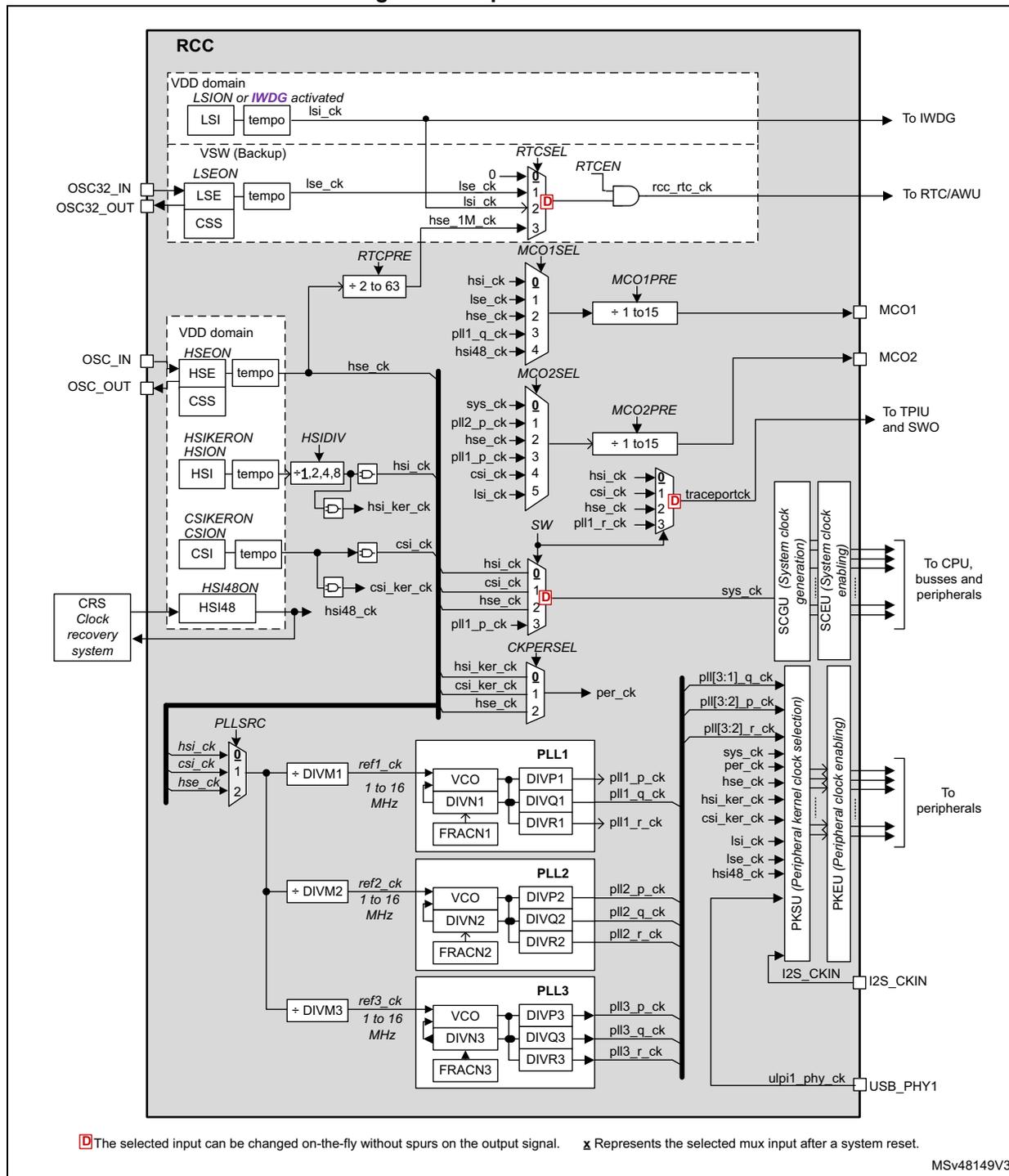
The diagram illustrates the top-level clock tree for the RCC. It shows the following components and paths:
- RCC Block:
The central component containing all clock logic.
- VDD domain: Contains LSI (tempo), LSE (tempo), and CSS. LSI is activated by LSION or IWDG. LSE is activated by LSEON. CSS is connected to OSC32_IN/OUT.
- VSW (Backup): Contains LSEON.
- VDD domain (HSE): Contains HSE (tempo) and CSS. HSE is activated by HSEON. CSS is connected to OSC_IN/OUT.
- HSI: Activated by HSION. tempo is connected to HSI. HSI is divided by HSDIV (+1,2,4,8) to produce hsi_ck and hsi_ker_ck.
- CSI: Activated by CSION. tempo is connected to CSI. CSI is divided to produce csi_ck and csi_ker_ck.
- HSI48: Activated by HSI48ON. tempo is connected to HSI48. HSI48 is divided to produce hsi48_ck.
- CRS Clock recovery system: Connected to the HSI48 path.
- RTC: Includes RTCSEL, RTCPRE (+2 to 63), and RTCCEN. It generates rcc_rtc_ck for the RTC/AWU.
- MCO1 and MCO2: Output clocks generated by MCO1SEL and MCO2SEL multiplexers and their respective dividers (MCO1PRE and MCO2PRE).
- traceportck: Generated by a multiplexer (SW) and its divider.
- SCGJ (System clock generation) and SCEU (System clock enabling): Generate sys_ck for the CPU, busses, and peripherals.
- PKSU (Peripheral kernel clock selection) and PKEU (Peripheral clock enabling): Generate peripheral clocks for various modules.
- PLL1, PLL2, and PLL3: Each consists of a VCO, DIVN, FRACN, DIVP, DIVQ, and DIVR. PLL1 generates pll1_p_ck, pll1_q_ck, and pll1_r_ck. PLL2 generates pll2_p_ck, pll2_q_ck, and pll2_r_ck. PLL3 generates pll3_p_ck, pll3_q_ck, and pll3_r_ck.
- CKPERSSEL: Generates per_ck from hsi_ker_ck, csi_ker_ck, or hse_ck.
- I2S_CKIN: Generated from sys_ck.
- ulpi1_phy_ck: Generated from ulpi1_phy_ck input.
- External Connections:
- OSC32_IN, OSC32_OUT: External 32 kHz oscillator pins.
- OSC_IN, OSC_OUT: External high-speed oscillator pins.
- To IWDG: Watchdog timer clock input.
- To RTC/AWU: Real-time clock and auto-wakeup clock input.
- To TPIU and SWO: Trace port and SWO clock input.
- To CPU, busses and peripherals: System clock output.
- To peripherals: Peripheral clock outputs.
- USB_PHY1: USB PHY clock input.
Legend:
- D: The selected input can be changed on-the-fly without spurs on the output signal.
- X: Represents the selected mux input after a system reset.
MSV48149V3
8.5.1 Clock naming convention
The RCC provides clocks to the complete circuit. To avoid misunderstanding, the following terms are used in this document:
- • Peripheral clocks
The peripheral clocks are the clocks provided by the RCC to the peripherals. Two kinds of clock are available:
- – bus interface clocks
- – kernel clocks
A peripheral receives from the RCC a bus interface clock in order to access its registers, and thus control the peripheral operation. This clock is generally the AHB, APB or AXI clock depending on which bus the peripheral is connected to. Some peripherals only need a bus interface clock (such as RNG, TIMx).
Some peripherals also require a dedicated clock to handle the interface function. This clock is named kernel clock. As an example, peripherals such as SAI must generate specific and accurate master clock frequencies, which require dedicated kernel clock frequencies. Another advantage of decoupling the bus interface clock from the specific interface needs, is that the bus clock can be changed without reprogramming the peripheral.
- • CPU clock
The CPU clock is the clock provided to the CPU. It is derived from the system clock ( sys_ck ).
- • Bus matrix clocks
The bus matrix clocks are the clocks provided to the different bridges (APB, AHB or AXI). These clocks are derived from the system clock ( sys_ck ).
8.5.2 Oscillators description
HSE oscillator
The HSE block can generate a clock from two possible sources:
- • external crystal/ceramic resonator
- • external clock source
Figure 48. HSE/LSE clock source
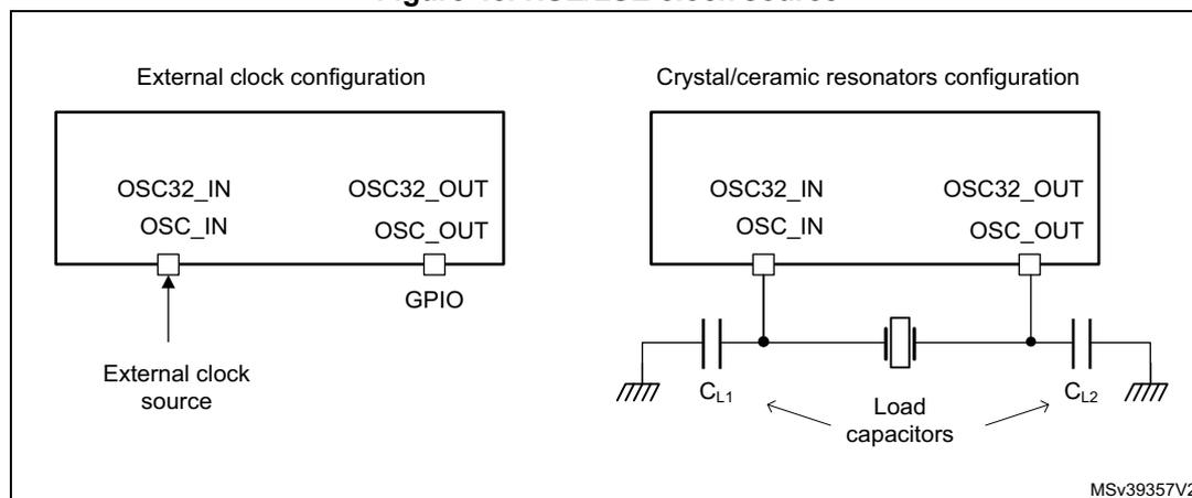
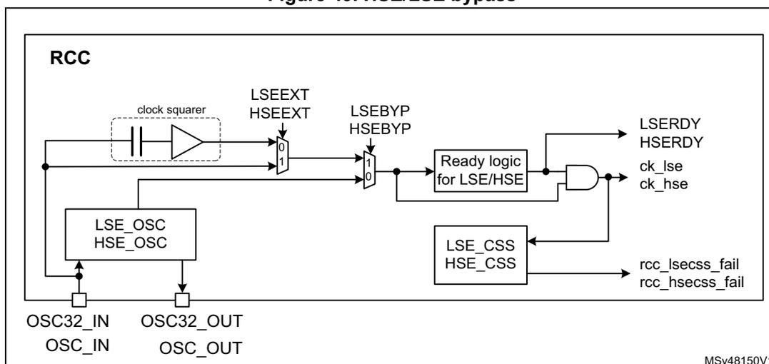
Figure 49. HSE/LSE bypass
External clock source (HSE bypass)
In this mode, an external clock source must be provided to OSC_IN pin. The external clock can be low swing (analog) or digital.
If this clock is directly used by a peripheral, the duty cycle requirement is defined by this peripheral and the application (refer to datasheet for more details)
This external clock is provided to the OSC_IN pin while the OSC_OUT pin must be left HI-Z (see Figure 48).
In case of an analog clock (low swing) the HSEBYP and HSEON bits must be set to 1 in the RCC source control register (RCC_CR) .
In case of a digital clock, the HSEBYP and the HSEEXT bits must be set to 1 followed by setting the HSEON bit to 1 in the RCC source control register (RCC_CR) .
External crystal/ceramic resonator
The oscillator is enabled by setting the HSEBYP bit to 0 and HSEON bit to 1.
The HSE can be used when the product requires a very accurate high-speed clock.
The associated hardware configuration is shown in Figure 48: the resonator and the load capacitors must be placed as close as possible to the oscillator pins in order to minimize output distortion and startup stabilization time. The loading capacitance values must be adjusted according to the selected crystal or ceramic resonator. Refer to the electrical characteristics section of the datasheet for more details.
The HSERDY flag of the RCC source control register (RCC_CR) indicates whether the HSE oscillator is stable or not. At startup, the hse_ck clock is not released until this bit is set by hardware. An interrupt can be generated if enabled in the RCC clock source interrupt enable register (RCC_CIER) .
The HSE can be switched ON and OFF through the HSEON bit. Note that the HSE cannot be switched OFF if one of the two conditions is met:
- • The HSE is used directly (via software mux) as system clock.
- • The HSE is selected as reference clock for PLL1, with PLL1 enabled and selected to provide the system clock (via software mux).
In that case the hardware does not allow programming the HSEON bit to 0.
The HSE is automatically disabled by hardware, when the system enters Stop or Standby mode (refer to Section 8.5.7: Handling clock generators in Stop and Standby modes for additional information).
In addition, the HSE clock can be driven to the MCO1 and MCO2 outputs and used as clock source for other application components.
LSE oscillator
The LSE block can generate a clock from two possible sources:
- • external crystal/ceramic resonator
- • external user clock
External clock source (LSE bypass)
In this mode, an external clock source must be provided to OSC32_IN pin. The input clock can have a frequency up to 1 MHz and be low swing (analog) or digital. A duty cycle close to 50% is recommended.
This external clock is provided to the OSC32_IN pin while the OSC32_OUT pin must be left HI-Z (see Figure 48 ).
In case of an analog clock (low swing) the LSEBYP and HSEON bits must be set to 1 ( RCC Backup domain control register (RCC_BDCR) ).
In case of a digital clock the LSEBYP and the LSEEXT bits must be set to 1 followed by setting the LSEON bit to 1 ( RCC Backup domain control register (RCC_BDCR) )
If the RTC is used, the LSE bypass must not be configured in digital mode but in low swing analog mode (default value after reset)
External crystal/ceramic resonator (LSE crystal)
The LSE clock is generated from a 32.768 kHz crystal or ceramic resonator. It has the advantage to provide a low-power highly accurate clock source to the real-time clock (RTC) for clock/calendar or other timing functions.
The LSERDY flag of the RCC Backup domain control register (RCC_BDCR) indicates whether the LSE crystal is stable or not. At startup, the LSE crystal output clock signal is not released until this bit is set by hardware. An interrupt can be generated if enabled in the RCC clock source interrupt enable register (RCC_CIER) .
The LSE oscillator is switched ON and OFF using the LSEON bit. The LSE remains enabled when the system enters Stop or Standby mode.
In addition, the LSE clock can be driven to the MCO1 output and used as clock source for other application components.
The LSE also offers a programmable driving capability (LSEDRV[1:0]) that can be used to modulate the amplifier driving capability. This driving capability is chosen according to the external crystal/ceramic component requirement to insure a stable oscillation.
The driving capability must be set before enabling the LSE oscillator.
HSI oscillator
The HSI block provides the default clock to the product.
The HSI is a high-speed internal RC oscillator that can be used directly as system clock, peripheral clock, or as PLL input. A prescaler allows the application to select an HSI output frequency of 8, 16, 32 or 64 MHz. This prescaler is controlled by the HSIDIV.
The HSI advantages are the following:
- • low-cost clock source since no external crystal is required
- • faster startup time than HSE (a few microseconds)
The HSI frequency, even with frequency calibration, is less accurate than an external crystal oscillator or ceramic resonator.
The HSI can be switched ON and OFF using the HSION bit. Note that the HSI cannot be switched OFF if one of the two conditions is met:
- • The HSI is used directly (via software mux) as system clock.
- • The HSI is selected as reference clock for PLL1, with PLL1 enabled and selected to provide the system clock (via software mux).
In that case the hardware does not allow programming the HSION bit to 0.
Note that the HSIDIV cannot be changed if the HSI is selected as reference clock for at least one enabled PLL (PLLxON bit set to 1). In that case the hardware does not update the HSIDIV with the new value. However it is possible to change the HSIDIV if the HSI is used directly as system clock.
The HSIRDY flag indicates if the HSI is stable or not. At startup, the HSI output clock is not released until this bit is set by hardware.
The HSI clock can also be used as a backup source (auxiliary clock) if the HSE fails (refer to CSS on HSE on page 355 ). The HSI can be disabled or not when the system enters Stop mode. Refer to Section 8.5.7: Handling clock generators in Stop and Standby modes for additional information.
In addition, the HSI clock can be driven to the MCO1 output and used as clock source for other application components.
Care must be taken when the HSI is used as kernel clock for communication peripherals, the application must take into account the following parameters:
- • the time interval between the moment where the peripheral generates a kernel clock request and the moment where the clock is really available,
- • the frequency accuracy.
Note: The HSI can remain enabled when the system is in Stop mode (see Section 8.5.7: Handling clock generators in Stop and Standby modes for additional information).
HSION, HSIRDY and HSIDIV bits are located in the RCC source control register (RCC_CR) .
HSI calibration
RC oscillator frequencies can vary from one chip to another due to manufacturing process variations. That is why each device is factory calibrated by STMicroelectronics to achieve an accuracy of ACC HSI (refer to the product datasheet for more information).
After a power-on reset, the factory calibration value is loaded in the HSICAL[11:0] bits.
If the application is subject to voltage or temperature variations, this may affect the RC oscillator frequency. The user application can trim the HSI frequency using the HSITRIM[6:0] bits.
Note: HSICAL[11:0] and HSITRIM[6:0] bits are located in the RCC CSI calibration register (RCC_CSICFGR).
Figure 50. HSI calibration flow
![Figure 50. HSI calibration flow diagram. The diagram shows the flow of calibration data from Engineering option bytes (factory calibration) through the RCC to the HSI. The RCC contains a summation node (+) that adds the value from FLASH_HSI_opt[8:0] to the value from HSITRIM[6:0] (unsigned). The result is stored in HSICAL[11:9] and HSICAL[8:0] within the RCC_CSICFGR register. These values are then passed to the HSI's CAL[11:0] register. The diagram also shows FLASH_HSI_opt[11:9] being passed directly to the HSI. The diagram is labeled MSV48151V2.](/RM0455-STM32H7A3-7B3-7B0/51ce2fc3e1003dd13cad1d99466e575d_img.jpg)
CSI oscillator
The CSI is a low-power RC oscillator that can be used directly as system clock, peripheral clock, or PLL input.
The CSI advantages are the following:
- • low-cost clock source since no external crystal is required
- • faster startup time than HSE (a few microseconds)
- • very low-power consumption,
The CSI provides a clock frequency of about 4 MHz, while the HSI is able to provide a clock up to 64 MHz.
CSI frequency, even with frequency calibration, is less accurate than an external crystal oscillator or ceramic resonator.
The CSI can be switched ON and OFF through the CSION bit. The CSIRDY flag indicates whether the CSI is stable or not. At startup, the CSI output clock is not released until this bit is set by hardware.
The CSI cannot be switched OFF if one of the two conditions is met:
- • The CSI is used directly (via software mux) as system clock.
- • The CSI is selected as reference clock for PLL1, with PLL1 enabled and selected to provide the system clock (via software mux).
In that case the hardware does not allow programming the CSION bit to 0.
The CSI can be disabled or not when the system enters Stop mode (refer to Section 8.5.7: Handling clock generators in Stop and Standby modes for additional information).
In addition, the CSI clock can be driven to the MCO2 output and used as clock source for other application components.
Even if the CSI settling time is faster than the HSI, care must be taken when the CSI is used as kernel clock for communication peripherals: the application must take into account the following parameters:
- • the time interval between the moment where the peripheral generates a kernel clock request and the moment where the clock is really available,
- • the frequency precision.
Note: CSION and CSIRDY bits are located in the RCC source control register (RCC_CR) .
CSI calibration
RC oscillator frequencies can vary from one chip to another due to manufacturing process variations, this is why each device is factory calibrated by STMicroelectronics to achieve accuracy of ACC CSI (refer to the product datasheet for more information).
After reset, the factory calibration value is loaded in the CSICAL[7:0] bits.
If the application is subject to voltage or temperature variations, this may affect the RC oscillator frequency. The user application can trim the CSI frequency using the CSITRIM[5:0] bits.
Note: Bits CSICAL[7:0] and CSITRIM[5:0] are located into the RCC CSI calibration register (RCC_CSICFGR) .
Figure 51. CSI calibration flow
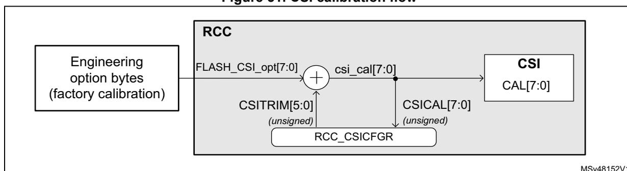
The diagram illustrates the CSI calibration logic. On the left, a block labeled "Engineering option bytes (factory calibration)" provides a signal FLASH_CSI_opt[7:0] to the RCC block. Inside the RCC block, this signal enters a summation node (+). The other input to the summation node is CSITRIM[5:0] (unsigned) , which comes from a register field within the RCC_CSICFGR register. The output of the summation node is csi_cal[7:0] , which is fed into the CSI block's CAL[7:0] register. Additionally, the RCC_CSICFGR register provides the CSICAL[7:0] (unsigned) value directly to the CSI block.
HSI48 oscillator
The HSI48 is an RC oscillator delivering a 48 MHz clock that can be used directly as kernel clock for some peripherals.
The HSI48 oscillator mainly aims at providing a high-precision clock to the USB peripheral by means of a special clock recovery system (CRS) circuitry, that can use the USB SOF signal, the LSE or an external signal to automatically adjust the oscillator frequency on-the-fly, with a very small granularity.
The HSI48 oscillator is disabled as soon as the system enters Stop or Standby mode. When the CRS is not used, this oscillator is free running and thus subject to manufacturing process variations. That is why each device is factory calibrated by STMicroelectronics to achieve an accuracy of ACC HSI48 (refer to the product datasheet for more information).
For more details on how to configure and use the CRS, refer to Section 9: Clock recovery system (CRS) .
The HSI48RDY flag indicates whether the HSI48 oscillator is stable or not. At startup, the HSI48 output clock is not released until this bit is set by hardware.
The HSI48 can be switched ON and OFF using the HSI48ON bit.
The HSI48 clock can also be driven to the MCO1 multiplexer and used as clock source for other application components.
Note: HSI48ON and HSI48RDY bits are located in the RCC source control register (RCC_CR) .
LSI oscillator
The LSI acts as a low-power clock source that can be kept running when the system is in Stop or Standby mode for the independent watchdog (IWDG) and auto-wake-up unit (AWU). The clock frequency is around 32 kHz. For more details, refer to the electrical characteristics section of the datasheet.
The LSI can be switched ON and OFF using the LSION bit. The LSIRDY flag indicates whether the LSI oscillator is stable or not. If an independent watchdog is started either by hardware or software, the LSI is forced ON and cannot be disabled.
The LSI remains enabled when the system enters Stop or Standby mode (refer to Section 8.5.7: Handling clock generators in Stop and Standby modes for additional information).
At LSI startup, the clock is not provided until the hardware sets the LSIRDY bit. An interrupt can be generated if enabled in the RCC clock source interrupt enable register (RCC_CIER) .
In addition, the LSI clock can be driven to the MCO2 output and used as a clock source for other application components.
Note: Bits LSION and LSIRDY bits are located into the RCC clock control and status register (RCC_CSR) .
8.5.3 Clock security system (CSS)
CSS on HSE
The clock security system can be enabled by software via the HSECSSON bit. The HSECSSON bit can be enabled even when the HSEON is set to 0.
The CSS on HSE is enabled by the hardware when the HSE is enabled and ready, and HSECSSON set to 1.
The CSS on HSE is disabled when the HSE is disabled. As a result, this function does not work when the system is in Stop mode.
It is not possible to clear directly the HSECSSON bit by software.
The HSECSSON bit is cleared by hardware when a system reset occurs or when the system enters Standby mode (see Section 8.4.2: System reset ).
If a failure is detected on the HSE clock, the system automatically switches to the HSI in order to provide a safe clock. The HSE is then automatically disabled, a clock failure event is sent to the break inputs of advanced-control timers (TIM1, TIM8, TIM15, TIM16, and TIM17), and an interrupt is generated to inform the software about the failure (CSS interrupt: rcc_hsecss_it ), thus allowing the MCU to perform rescue operations. If the HSE output was used as clock source for PLLs when the failure occurred, the PLLs are also disabled.
If an HSE clock failure occurs when the CSS is enabled, the CSS generates an interrupt that causes the automatic generation of an NMI. The HSECSSF flag in RCC clock source interrupt flag register (RCC_CIFR) is set to 1 to allow the application to identify the failure
source. The NMI routine is executed indefinitely until the HSECSSF bit is cleared. As a consequence, the application must clear the HSECSSF flag in the NMI ISR by setting the HSECSSC bit in the RCC clock source interrupt clear register (RCC_CICR) .
CSS on LSE
A clock security system on the LSE oscillator can be enabled by software by programming the LSECSSON bit in the RCC Backup domain control register (RCC_BDCR) .
This bit can be disabled only by hardware one of the following conditions is met:
- • after a pwr_vsw_rst ( \( V_{SW} \) software reset)
- • after a failure detection on LSE.
The LSECSSON bit must be written after the LSE is enabled (LSEON bit set by software) and ready (LSERDY set by hardware), and after the RTC clock has been selected through the RTCSEL bit.
The CSS on LSE works in all modes (Run, Stop and Standby) except VBAT.
If an LSE failure is detected, the LSE clock is no more delivered to the RTC but the values of RTCSEL, LSECSSON and LSEON bits are not changed by the hardware.
A wake-up is generated in Standby mode. In other modes an interrupt ( rcc_lsecss_it ) can be sent to wake up the software. The software must then disable the LSECSSON bit, stop the defective LSE (clear LSEON bit) and can change the RTC clock source (no clock or LSI or HSE) through RTCSEL bits, or take any required action to secure the application.
8.5.4 Clock output generation (MCO1/MCO2)
Two microcontroller clock output pins (MCO), MCO1 and MCO2, are available. A clock source can be selected for each output. The selected clock can be divided thanks to configurable prescaler (refer to Figure 47 for additional information on signal selection).
MCO1 and MCO2 outputs are controlled via MCO1PRE[3:0], MCO1[2:0], MCO2PRE[3:0] and MCO2[2:0] located in the RCC clock configuration register (RCC_CFGR) .
The GPIO port corresponding to each MCO pin must be programmed in alternate function mode.
The clock provided to the MCOs outputs must not exceed the maximum pin speed (refer to the product datasheet for information on the supported pin speed).
8.5.5 PLL description
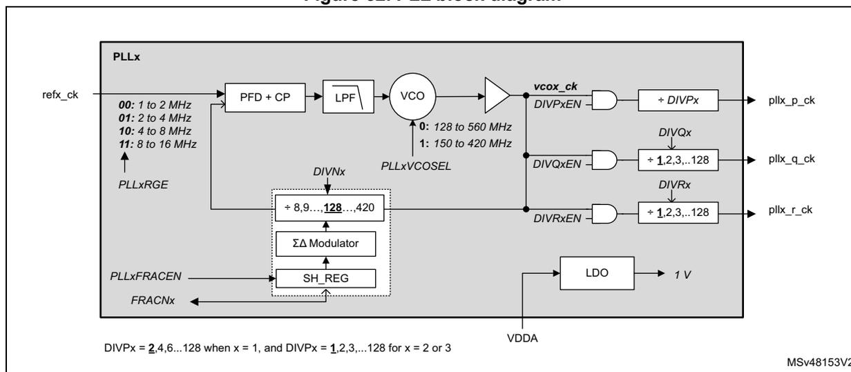
The RCC features three PLLs:
- • a main PLL, PLL1, generally used to provide clocks to the CPU and some peripherals
- • two dedicated PLLs, PLL2 and PLL3, used to generate the kernel clock for peripherals
The PLLs integrated into the RCC are completely independent. They offer the following features:
- • A VCO supporting two modes:
- – A wide-range
- – A low-range used for instance in audio application cases
- • Input frequency range:
- – 2 to 16 MHz for the VCO in wide-range mode
- – 1 to 2 MHz for the VCO in low-range mode
- • Capability to work either in integer or fractional mode
- • 13-bit sigma-delta modulator, allowing to fine-tune the VCO frequency by steps of 11 to 0.3 ppm
- • The sigma-delta modulator can be updated on-the-fly without generating frequency overshoots on PLLs outputs.
- • Each PLL offers 3 outputs with post-dividers.
Figure 52. PLL block diagram
graph LR
    refx_ck --> PFD_CP[PFD + CP]
    PFD_CP --> LPF[LPF]
    LPF --> VCO[VCO]
    VCO --> vcox_ck
    vcox_ck --> DIVPxEN[DIVPxEN Switch]
    vcox_ck --> DIVQxEN[DIVQxEN Switch]
    vcox_ck --> DIVRxEN[DIVRxEN Switch]
    DIVPxEN --> DIVPx["÷ DIVPx"] --> pll_p_ck
    DIVQxEN --> DIVQx["÷ 1,2,3...128"] --> pll_q_ck
    DIVRxEN --> DIVRx["÷ 1,2,3...128"] --> pll_r_ck
    vcox_ck --> DIVNx["÷ 8,9...128...420"]
    DIVNx --> PFD_CP
    SD_Mod[ΣΔ Modulator] --> DIVNx
    SH_REG --> SD_Mod
    PLLxFRACEN --> SD_Mod
    FRACNx --> SH_REG
    PLLxRGE --> PFD_CP
    PLLxVCOSEL --> VCO
    VDDA --> LDO --> 1V
Note: DIVPx = 2,4,6...128 when x = 1, and DIVPx = 1,2,3...128 for x = 2 or 3
The PLLs are controlled via RCC_PLLxDIVR, RCC_PLLxFRACR, RCC_PLLCFGR and RCC_CR registers.
The frequency of the reference clock provided to the PLLs ( refx_ck ) must range from 1 to 16 MHz. The DIVMx dividers of the RCC PLLs clock source selection register (RCC_PLLCKSELR) must be properly programmed in order to match this condition. In addition, the PLLxRGE[1:0] field of the RCC PLLs configuration register (RCC_PLLCFGR) must be set according to the reference input frequency to guarantee an optimal performance of the PLL.
The user application can then configure the proper VCO. The smaller range (150-420 MHz) must be chosen when the reference clock frequency is lower to 2 MHz.
To reduce the power consumption, it is recommended to configure the VCO output to the smaller range.
DIVNx loop divider must be programmed to achieve the expected frequency at VCO output. In addition, the VCO output range must be respected.
The PLLs operate in integer mode when the value of SH_REG bit of the FRACNx shadow register is set to 0. The SH_REG bit is updated with the FRACNx value when PLLxFRACEN bit goes from 0 to 1. The sigma-delta modulator is designed in order to minimize the jitter impact while allowing very small frequency steps.
The PLLs can be enabled by setting PLLxON to 1. The PLLxRDY bits indicate that the PLL is ready (means locked).
Note: Before enabling the PLLs, make sure that the reference frequency (refx_ck) provided to the PLL is stable, so the hardware does not allow changing DIVMx when the PLLx is ON and it is also not possible to change PLLSRC when one of the PLL is ON.
The hardware prevents writing PLL1ON to 0 if the PLL1 is currently used to deliver the system clock. There are other hardware protections on the clock generators (refer to HSE oscillator on page 349 , HSI oscillator on page 352 and CSI oscillator on page 353 ).
The following PLL parameters cannot be changed once the PLL is enabled: DIVNx, PLLxRGE, PLLxVCOSEL, DIVPx, DIVQx, DIVRx, DIVPxEN, DIVQxEN and DIVRxEN.
To insure an optimal behavior of the PLL when one of the post-divider (DIVP, DIVQ or DIVR) is not used, the application must set the enable bit (DIVyEN) as well as the corresponding post-divider bits (DIVP, DIVQ or DIVR) to 0.
If the above rules are not respected, the PLL output frequency is not guaranteed.
Output frequency computation
When the PLL is configured in integer mode (SH_REG = 0), the VCO frequency ( \( F_{VCO} \) ) is given by the following expression:
When the PLL is configured in fractional mode (SH_REG different from 0), the DIVN divider must be initialized before enabling the PLLs. However, it is possible to change the value of FRACNx on-the-fly without disturbing the PLL output.
This feature can be used either to generate a specific frequency from any crystal value with a good accuracy or to fine-tune the frequency on-the-fly.
For each PLL, the VCO frequency is given by the following formula:
Note: For PLL1, DIVP can only take odd values.
The PLLs are disabled by hardware when:
- • the system enters Stop or Standby mode
- • an HSE failure occurs when HSE or PLL (clocked by HSE) are used as system clock
PLL initialization phase
Figure 53 shows the recommended PLL initialization sequence in integer and fractional mode. The PLLx are supposed to be disabled at the start of the initialization sequence:
- 1. Initialize the PLLs registers according to the required frequency.
- – Set PLLxFRACEN of RCC PLLs configuration register (RCC_PLLCFGR) to 0 for integer mode.
- – For fractional mode, set FRACN to the required initial value (FracInitValue) and then set PLLxFRACEN to 1.
- 2. Once the PLLxON bit is set to 1, the user application must wait until PLLxRDY bit is set to 1. If the PLLx is in fractional mode, the PLLxFRACEN bit must not be set back to 0 as long as PLLxRDY = 0.
- 3. Once the PLLxRDY bit is set to 1, the PLLx is ready to be used.
- 4. If the application intends to tune the PLLx frequency on-the-fly (possible only in fractional mode), then:
- a) PLLxFRACEN must be set to 0. When PLLxFRACEN = 0, the sigma-delta modulator is still operating with the value latched into SH_REG.
- b) A new value must be uploaded into PLLxFRACR (FracValue(n)).
- c) PLLxFRACEN must be set to 1, in order to latch the content of PLLxFRACR into its shadow register.
Note: When the PLLxRDY goes to 1, it means that the difference between the PLLx output frequency and the target value is lower than \( \pm 2\% \) .
Figure 53. PLLs Initialization flowchart
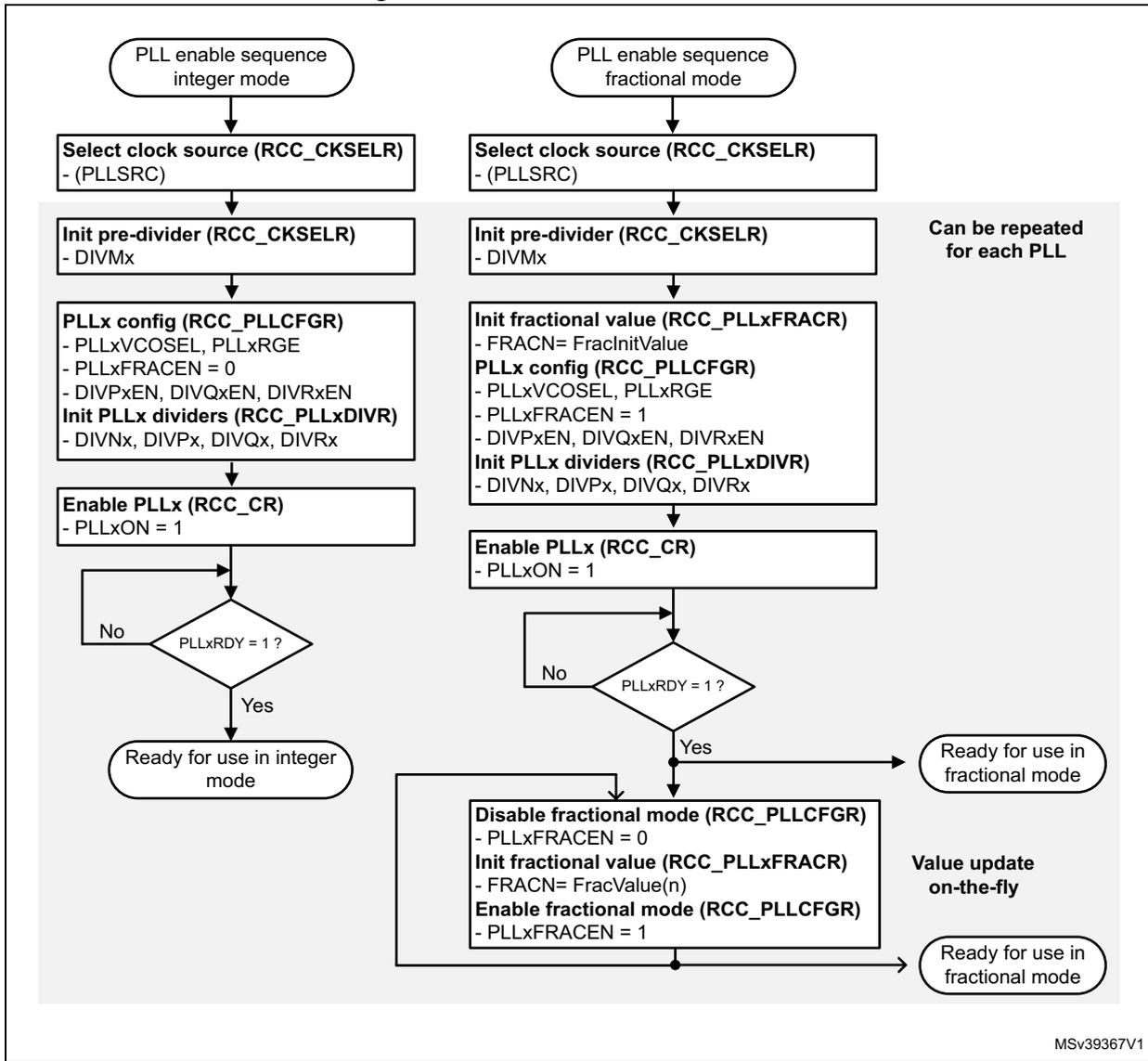
The flowchart illustrates the initialization process for PLLs, divided into two main paths: integer mode and fractional mode. Both paths start with a 'PLL enable sequence' (integer or fractional mode). The integer mode path consists of selecting a clock source (RCC_CKSELR), initializing a pre-divider (RCC_CKSELR), configuring the PLL (RCC_PLLCFGR), initializing dividers (RCC_PLLxDIVR), and enabling the PLL (RCC_CR). A loop exists until the PLL is ready (PLLxRDY = 1). The fractional mode path follows a similar structure but includes an additional step to initialize the fractional value (RCC_PLLxFRACR). A note indicates that the pre-divider initialization can be repeated for each PLL. A common block for 'Value update on-the-fly' shows how to disable fractional mode, update the fractional value, and re-enable it. The final states are 'Ready for use in integer mode' or 'Ready for use in fractional mode'.
graph TD; subgraph IntegerMode [ ]; A1([PLL enable sequence integer mode]) --> B1[Select clock source (RCC_CKSELR) - (PLL_SRC)]; B1 --> C1[Init pre-divider (RCC_CKSELR) - DIVMx]; C1 --> D1[PLLx config (RCC_PLLCFGR) - PLLxVCOSEL, PLLxRGE - PLLxFRACEN = 0 - DIVPxEN, DIVQxEN, DIVRxEN Init PLLx dividers (RCC_PLLxDIVR) - DIVNx, DIVPx, DIVQx, DIVRx]; D1 --> E1[Enable PLLx (RCC_CR) - PLLxON = 1]; E1 --> F1{PLLxRDY = 1?}; F1 -- No --> E1; F1 -- Yes --> G1([Ready for use in integer mode]); end; subgraph FractionalMode [ ]; A2([PLL enable sequence fractional mode]) --> B2[Select clock source (RCC_CKSELR) - (PLL_SRC)]; B2 --> C2[Init pre-divider (RCC_CKSELR) - DIVMx]; C2 --> D2[Init fractional value (RCC_PLLxFRACR) - FRACN= FracInitValue PLLx config (RCC_PLLCFGR) - PLLxVCOSEL, PLLxRGE - PLLxFRACEN = 1 - DIVPxEN, DIVQxEN, DIVRxEN Init PLLx dividers (RCC_PLLxDIVR) - DIVNx, DIVPx, DIVQx, DIVRx]; D2 --> E2[Enable PLLx (RCC_CR) - PLLxON = 1]; E2 --> F2{PLLxRDY = 1?}; F2 -- No --> E2; F2 -- Yes --> G2([Ready for use in fractional mode]); end; C2 -.-> H[Can be repeated for each PLL]; G2 --> I[Disable fractional mode (RCC_PLLCFGR) - PLLxFRACEN = 0 Init fractional value (RCC_PLLxFRACR) - FRACN= FracValue(n) Enable fractional mode (RCC_PLLCFGR) - PLLxFRACEN = 1]; I --> J([Ready for use in fractional mode]); I -.-> K[Value update on-the-fly];MSV39367V1
8.5.6 System clock (sys_ck)
System clock selection
After a system reset, the HSI is selected as system clock and all PLLs are switched OFF. When a clock source is used for the system clock, it is not possible for the software to disable the selected source via the xxxON bits.
Of course, the system clock can be stopped by the hardware when the system enters Stop or Standby mode.
When the system is running, the user application can select the system clock ( sys_ck ) among the 4 following sources:
- • HSE
- • HSI
- • CSI
- • pll1_p_ck
This function is controlled by programming the RCC clock configuration register (RCC_CFGR) . A switch from one clock source to another occurs only if the target clock source is ready (clock stable after startup delay or PLL locked). If a clock source that is not yet ready is selected, the switch occurs when the clock source is ready.
The SWS status bits in the RCC clock configuration register (RCC_CFGR) indicate which clock is currently used as system clock. The other status bits in the RCC_CR register indicate which clock(s) is (are) ready.
System clock generation
Figure 54 shows a simplified view of the clock distribution for the CPU and busses. All the dividers shown in the block diagram can be changed on-the-fly without generating timing violations. This feature is a very simple solution to adapt the busses frequencies to the application needs, thus optimizing the power consumption.
The CDCPRE divider can be used to adjust the CPU clock. However this also impacts the clock frequency of all bus matrix.
In the same way, HPRE divider can be used to adjust the clock for the CPU domain bus matrix, but this also impacts the clock frequency of bus matrix of SmartRun domain.
Most of the prescalers are controlled via RCC_CDCFGR and RCC_SRDCFGR registers.
Figure 54. Core and bus clock generation
![Figure 54. Core and bus clock generation diagram showing the RCC block, System clock generation (SCGU), and various clock outputs for CD and SRD domains. The diagram shows the flow from sys_ck through various prescalers (CDCPRE, HPRE, CDPPRE1, CDPPRE2, SRDPRE) to generate rcc_cpu_ck, rcc_folk, rcc_aclk, rcc_hclk3, rcc_pclk3, rcc_hclk[2:1], rcc_pclk1, rcc_timx_ker_ck, rcc_pclk2, rcc_timy_ker_ck, rcc_hclk4, rcc_folk_srd, and rcc_pclk4. These are then distributed to the CD domain (CPU clocks, CPU SysTick clock, AXI peripheral clocks, AHB3 peripheral clocks, APB3 peripheral clocks, AHB1 and 2 peripheral clocks, APB1 peripheral clocks, Timers prescaler clock, APB2 peripheral clocks, Timers prescaler clock) and the SRD domain (AHB4 peripheral clocks, APB4 peripheral clocks).](/RM0455-STM32H7A3-7B3-7B0/1a79c98873ad3bae4358d430c7d95e73_img.jpg)
(1) Can be changed on-the-fly. ⌄ Represents the selected mux input after a system reset. MSV48154V2
This block also provides the clock for the timers ( rcc_timx_ker_ck and rcc_timy_ker_ck ). The frequency of the timers clock depends on the APB prescaler corresponding to the bus to which the timer is connected, and on TIMPRE bit.
Table 55 shows how to select the timer clock frequency.
Table 55. Ratio between clock timer and pclk
| CDPPRE1
(1) CDPPRE2 | TIMPRE (2) | - | F
rcc_timx_ker_ck F rcc_timy_ker_ck | F
rcc_pclk1 F rcc_pclk2 | Comments |
|---|---|---|---|---|---|
| 0xx | 0 | → | F rcc_hclk1 | F rcc_hclk1 | The timer clock is equal to the bus clock. |
| 100 | 0 | → | F rcc_hclk1 | F rcc_hclk1 / 2 | The timer clock is twice as fast as the bus clock. |
| 101 | 0 | → | F rcc_hclk1 / 2 | F rcc_hclk1 / 4 | |
| 110 | 0 | → | F rcc_hclk1 / 4 | F rcc_hclk1 / 8 | |
| 111 | 0 | → | F rcc_hclk1 / 8 | F rcc_hclk1 / 16 |
Table 55. Ratio between clock timer and pclk (continued)
| CDPPRE1
(1) CDPPRE2 | TIMPRE (2) | - | F
rcc_timx_ker_ck F rcc_timy_ker_ck | F
rcc_pclk1 F rcc_pclk2 | Comments |
|---|---|---|---|---|---|
| 0xx | 1 | → | F rcc_hclk1 | F rcc_hclk1 | The timer clock is equal to the bus clock. |
| 100 | 1 | → | F rcc_hclk1 | F rcc_hclk1 / 2 | The timer clock is twice as fast as the bus clock. |
| 101 | 1 | → | F rcc_hclk1 | F rcc_hclk1 / 4 | The timer clock is 4 times faster than the bus clock. |
| 110 | 1 | → | F rcc_hclk1 / 2 | F rcc_hclk1 / 8 | |
| 111 | 1 | → | F rcc_hclk1 / 4 | F rcc_hclk1 / 16 |
1. CDPPRE1 and CDPPRE2 belong to RCC CPU domain clock configuration register 2 (RCC_CDCFGGR2) .
2. TIMPRE belongs to RCC clock configuration register (RCC_CFGR) .
8.5.7 Handling clock generators in Stop and Standby modes
When the whole system enters Stop mode, all the clocks (system and kernel clocks) are stopped as well as the following clock sources:
- • CSI, HSI (depending on HSIKERON, and CSIKERON bits)
- • HSE
- • PLL1, PLL2 and PLL3
- • HSI48
The content of the RCC registers is not altered except for PLL1ON, PLL2ON, PLL3ON, HSEON and HSI48ON that are set to 0.
Exiting Stop mode
When the microcontroller exits system Stop mode via a wake-up event, the application can select which oscillator (HSI and/or CSI) is used to restart. The STOPWUCK bit selects the oscillator used as system clock. The STOPKERWUCK bit selects the oscillator used as kernel clock for peripherals. The STOPKERWUCK bit is useful if after a system Stop, a peripheral needs a kernel clock generated by an oscillator different from the one used for the system clock.
All these bits belong to the RCC clock configuration register (RCC_CFGR) .
Table 56 gives a detailed description of their behavior.
Table 56. STOPWUCK and STOPKERWUCK description
| STOPWUCK | STOPKERWUCK | - | Activated oscillator when system exits Stop mode | Distributed clocks when system exits Stop mode | |
|---|---|---|---|---|---|
| System clock | Kernel clock | ||||
| 0 | 0 | → | HSI | HSI | HSI |
| 1 | → | HSI and CSI | HSI and/or CSI | ||
| 1 | 0 | → | HSI and CSI | CSI | HSI and/or CSI |
| 1 | → | CSI | CSI | ||
During Stop mode
There are two specific cases where the HSI or CSI can be enabled during system Stop mode:
- • when a dedicated peripheral requests the kernel clock
The peripheral receives the HSI or CSI according to the kernel clock source selected for this peripheral (via PERxSRC). - • when the HSIKERON or CSIKERON bits are set
The HSI and CSI are kept running during Stop mode but the outputs are gated. The clock is then available immediately when the system exits Stop mode or when a peripheral requests the kernel clock (see Table 57 for details).
HSIKERON and CSIKERON bits belong to RCC source control register (RCC_CR) .
Table 57 gives a detailed description of their behavior.
Table 57. HSIKERON and CSIKERON behavior
| HSIKERON (CSIKERON) | - | HSI (CSI) state during Stop mode | HSI (CSI) setting time |
|---|---|---|---|
| 0 | → | OFF | \( t_{su(HSI)} \) ( \( t_{su(CSI)} \) ) (1) |
| 1 | → | Running and gated | Immediate |
- 1. \( t_{su(HSI)} \) and \( t_{su(CSI)} \) are the startup times of the HSI and CSI oscillators (refer to the product datasheet for values of these parameters).
When the microcontroller exits system Standby mode, the HSI is selected as system and kernel clock. The RCC registers are reset to their initial values except for the RCC_RSR and RCC_BDCR registers.
Note that the HSI and CSI outputs provide two clock paths (see Figure 47 ):
- • one path for the system clock ( hsi_ck or csi_ck )
- • one path for the peripheral kernel clock ( hsi_ker_ck or csi_ker_ck ).
When a peripheral requests the kernel clock in system Stop mode, only the path providing the hsi_ker_ck or csi_ker_ck is activated.
Caution: It is not guaranteed that the CPU gets automatically the same clock frequencies when leaving CStop mode: this mainly depends on the system state. For example If the CPU goes to CStop, while the SmartRun domain is kept in CRun, the clock settings remain unchanged when the CPU exits from CStop. If the SmartRun domain goes to CStop while the CPU is also in CStop, then the CPU operates with HSI or CSI when exiting from CStop mode.
8.5.8 Kernel clock selection
Some peripherals are designed to work with two different clock domains that operate asynchronously:
- • a clock domain synchronous with the register and bus interface ( ckg_bus_perx clock)
- • a clock domain generally synchronous with the peripheral (kernel clock)
The benefit of having peripherals supporting these two clock domains is that the user application has more freedom to choose optimized clock frequency for the CPU, bus matrix and for the kernel part of the peripheral.
As a consequence, the user application can change the bus frequency without reprogramming the peripherals. As an example an on-going transfer with UART is not disturbed if its APB clock is changed on-the-fly.
Table 58 shows the kernel clock that the RCC can deliver to the peripherals. Each row of this table represents a mux and the peripherals connected to its output. The columns starting from number 4 represents the clock sources. Column 3 gives the maximum allowed frequency at each mux output. It is up to the user to respect these requirements.
Table 58. Kernel clock distribution overview
| Peripherals | Clock mux control bits | Domain | Clock sources (1) | |||||||||||||||||||
|---|---|---|---|---|---|---|---|---|---|---|---|---|---|---|---|---|---|---|---|---|---|---|
| pll1_q_ck | pll2_p_ck | pll2_q_ck | pll2_r_ck | pll3_p_ck | pll3_q_ck | pll3_r_ck | sys_ck | bus clocks (2) | hse_ck | hsi_ker_ck | csi_ker_ck | hsi48_ck | lse_ck | lsi_ck | per_ck (3) | I2S_CKIN | USB_PHY1 | spdifrx_symb_ck | Disabled | |||
| LTDC | - | CPU domain | - | - | - | - | - | - | x | - | - | - | - | - | - | - | - | - | - | - | - | - |
| FMC | FMCSEL | 1 | - | - | 2 | - | - | - | - | 0 | - | - | - | - | - | - | 3 | - | - | - | - | |
| OCTOSPI | OCTOSPISEL | 1 | - | - | 2 | - | - | - | - | 0 | - | - | - | - | - | - | 3 | - | - | - | - | |
| SDMMC1 (6) | SDMMCSEL | 0 | - | - | 1 | - | - | - | - | - | - | - | - | - | - | - | - | - | - | - | - | |
| SDMMC2 | - | - | - | - | - | - | - | - | - | - | - | - | - | - | - | - | - | |||||
| DFSDM1 Aclk | SAI1SEL | 0 | 1 | - | - | 2 | - | - | - | - | - | - | - | - | - | - | 4 | 3 | - | - | - | |
| DFSDM1 clk | DFSDM1SEL | - | - | - | - | - | - | - | 1 | 0 | - | - | - | - | - | - | - | - | - | - | - | |
| FDCAN | FDCANSEL | 1 | - | 2 | - | - | - | - | - | - | 0 | - | - | - | - | - | - | - | - | - | - | |
| HDMI-CEC | CECSEL | - | - | - | - | - | - | - | - | - | - | - | 2 (4) | - | 0 | 1 | - | - | - | - | - | |
| I2C1,2,3 | I2C123SEL | - | - | - | - | - | - | 1 | - | 0 | - | 2 | 3 | - | - | - | - | - | - | - | - | |
| LPTIM1 | LPTIM1SEL | - | 1 | - | - | - | - | 2 | - | 0 | - | - | - | - | 3 | 4 | 5 | - | - | - | - | |
| TIM[8:1], TIM[17:12] | - | - | - | - | - | - | - | - | - | x | - | - | - | - | - | - | - | - | - | - | - | |
| RNG | RNGSEL | 1 | - | - | - | - | - | - | - | - | - | - | - | 0 | 2 | 3 | - | - | - | - | - | |
| SAI1 (5) | SAI1SEL | 0 | 1 | - | - | 2 | - | - | - | - | - | - | - | - | - | - | 4 | 3 | - | - | - | |
| SAI2 | SAI2ASEL | 0 | 1 | - | - | 2 | - | - | - | - | - | - | - | - | - | - | 4 | 3 | - | 5 | - | |
| SAI2BSEL | - | - | - | - | - | - | - | - | - | - | - | - | - | - | - | - | - | |||||
Table 58. Kernel clock distribution overview (continued)
| Peripherals | Clock mux control bits | Domain | Clock sources (1) | |||||||||||||||||||
|---|---|---|---|---|---|---|---|---|---|---|---|---|---|---|---|---|---|---|---|---|---|---|
| pll1_q_ck | pll2_p_ck | pll2_q_ck | pll2_r_ck | pll3_p_ck | pll3_q_ck | pll3_r_ck | sys_ck | bus clocks (2) | hse_ck | hsi_ker_ck | csi_ker_ck | hsi48_ck | lse_ck | lsi_ck | per_ck (3) | i2s_ckin | usb_phy1 | spdifrx_symb_ck | Disabled | |||
| SPDIFRX | SPDIFRXSEL | CPU domain (continued) | 0 | - | - | 1 | - | - | 2 | - | - | - | 3 | - | - | - | - | - | - | - | - | - |
| SPI(I2S)1,2,3 | SPI123SEL | 0 | 1 | - | - | 2 | - | - | - | - | - | - | - | - | - | - | 4 | 3 | - | - | - | |
| SPI4,5 | SPI45SEL | - | - | 1 | - | - | 2 | - | - | 0 | 5 | 3 | 4 | - | - | - | - | - | - | - | - | |
| SWPMI | SWPMISEL | - | - | - | - | - | - | - | - | 0 | - | 1 | - | - | - | - | - | - | - | - | - | |
| USART1,6,10 UART9 | USART16910 SEL | - | - | 1 | - | - | 2 | - | - | 0 | - | 3 | 4 | - | 5 | - | - | - | - | - | - | |
| USART2,3 UART4,5, 7,8 | USART234578 SEL | - | - | 1 | - | - | 2 | - | - | 0 | - | 3 | 4 | - | 5 | - | - | - | - | - | - | |
| USB1OTG | USBSEL | 1 | - | - | - | - | 2 | - | - | - | - | - | - | 3 | - | - | - | - | - | - | 0 | |
| USB1ULPI | - | - | - | - | - | - | - | - | - | - | - | - | - | - | - | - | - | - | x | - | - | |
| ADC1,2 (6) | ADCSEL | - | 0 | - | - | - | - | 1 | - | - | - | - | - | - | - | - | 2 | - | - | - | - | |
| DAC1 | - | - | - | - | - | - | - | - | - | - | - | - | - | - | - | x | - | - | - | - | - | |
| I2C4 | I2C4SEL | SmartRun domain | - | - | - | - | - | - | 1 | - | 0 | - | 2 | 3 | - | - | - | - | - | - | - | - |
| LPUART1 | LPUART1SEL | - | - | 1 | - | - | 2 | - | - | 0 | - | 3 | 4 | - | 5 | - | - | - | - | - | - | |
| SPI6(I2S) (7) | SPI6SEL | - | - | 1 | - | - | 2 | - | - | 0 | 5 | 3 | 4 | - | - | - | - | 6 | - | - | - | |
| DFSDM2 Aclk | SPI6SEL | - | - | 1 | - | - | 2 | - | - | 0 | 5 | 3 | 4 | - | - | - | - | - | - | - | - | |
| DFSDM2 clk | DFSDM2SEL | - | - | - | - | - | - | - | 1 | 0 | - | - | - | - | - | - | - | - | - | - | - | |
| LPTIM2 | LPTIM2SEL | - | 1 | - | - | - | - | 2 | - | 0 | - | - | - | - | 3 | 4 | 5 | - | - | - | - | |
| LPTIM3 | LPTIM3SEL | - | 1 | - | - | - | - | 2 | - | 0 | - | - | - | - | 3 | 4 | 5 | - | - | - | - | |
| DAC2 | - | - | - | - | - | - | - | - | - | - | - | - | - | - | - | x | - | - | - | - | - | |
| RTC/AWU | RTCSEL | VSW | - | - | - | - | - | - | - | - | - | 3 (8) | - | - | - | 1 | 2 | - | - | - | - | 0 |
- 1. X represents the selected mux input after a system reset.
- 2. The bus clocks are the bus interface clocks to which the peripherals are connected. It can be APB, AHB or AXI clocks.
- 3. The per_ck clock can be hse_ck, hsi_ker_ck or csi_ker_ck according to CKPERSEL selection.
- 4. Clock CSI divided by 122.
- 5. The SAI1 max clock frequency can, in some cases, be limited by the constraints on DFSDM1 (see Figure 55).
- 6. With a duty cycle close to 50 %, meaning that DIV[P/Q/R]x values must be even. For SDMMCx, the duty cycle must be 50 % when supporting DDR.
- 7. The SPI6 maximum clock frequency can, in some cases, be limited by the constraints on DFSDM2 (see Figure 55 and Figure 56).
- 8. Clock HSE divided by RTCPRE.
Figure 55 to Figure 63 provide a more detailed description of kernel clock distribution. To simplify the drawings, the bus interface clocks (pclk, hclk) are not represented, even if they are gated with enable signals. Refer to Section 8.5.11: Peripheral clock gating control for more details.
To reduce the amount of switches, some peripherals share the same kernel clock source. Nevertheless, all peripherals have their dedicated enable signal.
Peripherals dedicated to audio applications
The audio peripherals generally need specific accurate frequencies, except for SPDIFRX. As shown in Figure 55 and Figure 58 , the kernel clock of the SAIs or SPI(I2S)s can be generated by:
- • PLL1 when the amount of active PLLs must be reduced (for SAIs and SPI/I2S1 to 3)
- • APB2 peripheral clock (for SPI/I2S4 and 5)
- • APB4 peripheral clock (for SPI/I2S6)
- • PLL2 or 3 for optimal flexibility in frequency generation
- • HSE, HSI or CSI for use-cases where the current consumption is critical
- • I2S_CKIN when an external clock reference needs to be used
Note: The SPDIFRX does not require a specific frequency but only a kernel clock frequency high enough to make the peripheral work properly. Refer to the SPDIFRX description for more details.
DFSDM1 can use the same clock as SAI1 and DFSDM2 can use the same clock as I2S6. This is useful when DFSDM1 and DFSDM2 are used for audio applications.
The SAI2 can use the symbol clock provided by the SPDIFRX. SPI/I2S1, 2, and 3 share the same kernel clock source. The SPI/I2S4 and 5 share the same kernel clock source (see Figure 56 ).
Figure 55. Kernel clock distribution for SAIs, DFSDMs and SPDIFRX
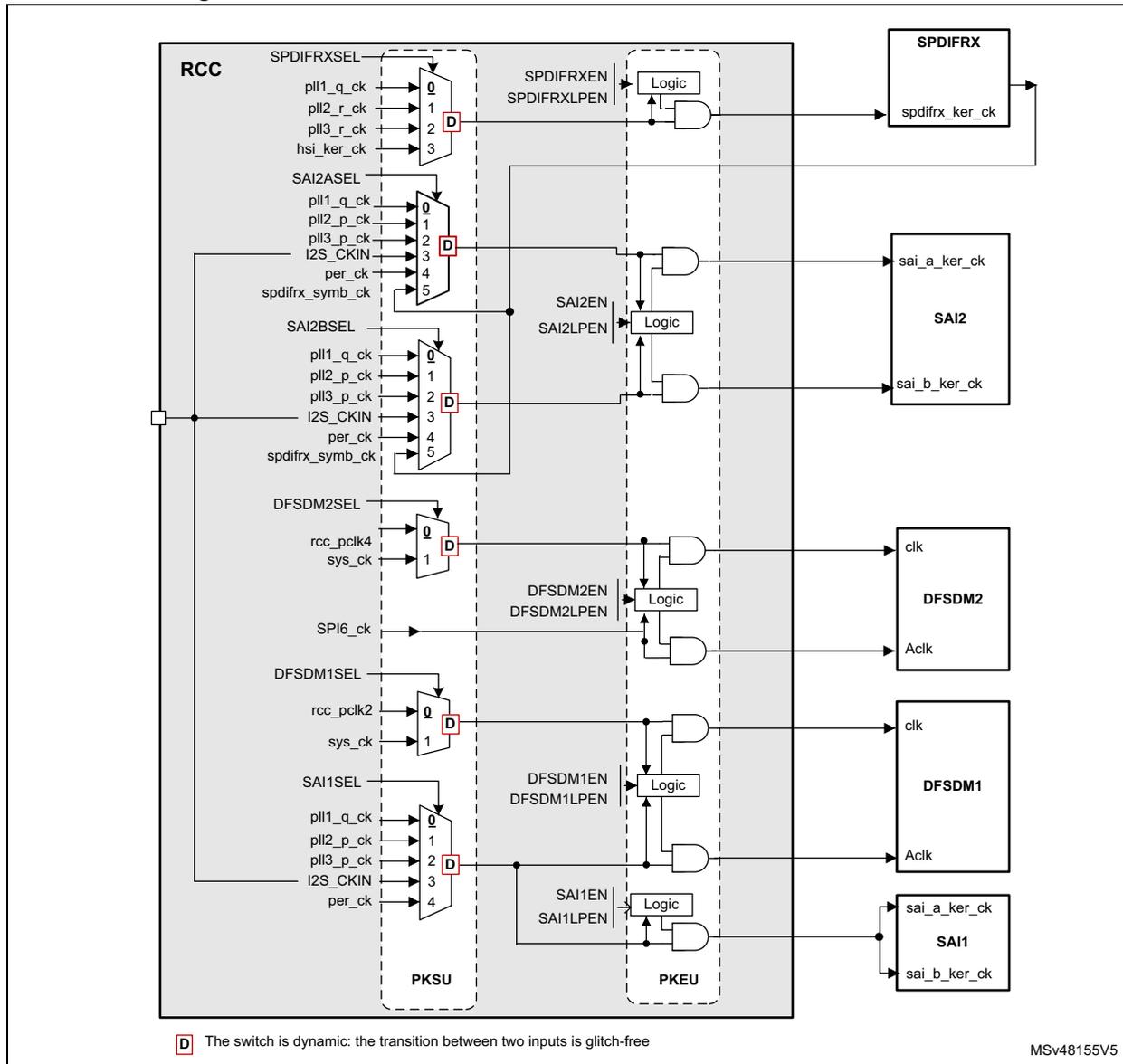
The diagram illustrates the internal clock distribution system. On the left, the RCC provides various clock signals. These are routed through multiplexers (MUX) to select the appropriate source for each peripheral. The selected clocks are then passed through 'Logic' blocks (PKEU) which act as gates, controlled by enable signals (e.g., SPDIFRXEN, SAI2EN, DFSDM2EN, DFSDM1EN, SAI1EN) and low-power enable signals (e.g., SPDIFRXLPEN, SAI2LPEN, DFSDM2LPEN, DFSDM1LPEN, SAI1LPEN). The gated clocks are then distributed to the peripherals: SPDIFRX, SAI2, DFSDM2, DFSDM1, and SAI1. A legend at the bottom left indicates that a 'D' in a box represents a dynamic switch where the transition between two inputs is glitch-free.
D The switch is dynamic: the transition between two inputs is glitch-free
MSV48155V5
- 1. X represents the selected mux input after a system reset.
- 2. This figure does not show the connection of the bus interface clock to the peripherals. For details on each enable cell, refer to Section 8.5.11: Peripheral clock gating control .
Peripherals dedicated to control and data transfer
Peripherals such as SPIs, I2Cs, UARTs do not need a specific kernel clock frequency but a clock fast enough to generate the correct baud rate, or the required bit clock on the serial interface. For that purpose the source can be selected among the following ones:
- • PLL1 when the amount of active PLLs must be reduced
- • PLL2 or PLL3 if better flexibility is required. As an example, this solution allows changing the frequency bus via PLL1 without affecting the speed of some serial interfaces.
- • HSI or CSI for low-power use-cases or when the peripheral must quickly wake up from Stop mode (such as UART or I2C)
Note: UARTs also need the LSE clock when high baud rates are not required.
Figure 56. Kernel clock distribution for SPIs and SPI/I2S
![Figure 56: Kernel clock distribution for SPIs and SPI/I2S. The diagram shows the RCC (Reset and Clock Control) block on the left, which contains three multiplexers (MUX) for SPI123, SPI45, and SPI6. Each MUX selects a clock source from various options (PLL1, PLL2, PLL3, HSI, CSI, HSE, I2S_CKIN, etc.). The selected clock is then passed through a logic block (AND gate) that also receives enable signals (SPI[3:1]EN, SPI[3:1]LPEN, SPI[5:4]EN, SPI[5:4]LPEN, SPI6AMEN, SPI6EN, SPI6LPEN). The output of the logic block is the kernel clock (spi_ker_ck) for the corresponding peripheral (SPI/I2S[3:1], SPI[5:4], SPI/I2S6). A note indicates that the switch is dynamic and glitch-free. The diagram also shows connections to DFSDM2 and PKEU blocks.](/RM0455-STM32H7A3-7B3-7B0/d857a816663b2bb31fd8fe42b2016004_img.jpg)
D The switch is dynamic: the transition between two inputs is glitch-free.
MSV48156V3
- 1. X represents the selected mux input after a system reset.
- 2. This figure does not show the connection of the bus interface clock to the peripheral. For details on each enable cell, refer to Section 8.5.11: Peripheral clock gating control .
Figure 57. Kernel clock distribution for I2Cs
![Schematic diagram of kernel clock distribution for I2Cs. It shows the RCC block containing PKSU and PKEU sub-blocks. PKSU has two 4-to-1 multiplexers. The top mux is for I2C4, with inputs rcc_pclk4 (0), pll3_r_ck (1, selected), hsi_ker_ck (2), and csi_ker_ck (3). The bottom mux is for I2C[3:1], with inputs rcc_pclk1 (0), pll3_r_ck (1, selected), hsi_ker_ck (2), and csi_ker_ck (3). Both selected mux outputs go to Logic blocks in PKEU. The top Logic block also takes I2C4AMEN, I2C4EN, and I2C4LPEN as inputs and outputs i2c_ker_ck_req and i2c_ker_ck to the I2C4 peripheral. The bottom Logic block takes I2C[3:1]EN and I2C[3:1]LPEN as inputs and outputs i2c_ker_ck_req and i2c_ker_ck to the I2C[3:1] peripheral. A legend indicates that 'D' in a red box means the switch is dynamic and glitch-free.](/RM0455-STM32H7A3-7B3-7B0/56d829bcd0079ac2e963ee6df7bf540e_img.jpg)
D The switch is dynamic: the transition between two inputs is glitch-free.
MSV48157V2
- 1. X represents the selected mux input after a system reset
- 2. This figure does not show the connection of the bus interface clock to the peripheral, for details on each enable cell, please refer to Section 8.5.11: Peripheral clock gating control .
Figure 58. Kernel clock distribution for UARTs, USARTs and LPUART1
![Figure 58: Kernel clock distribution for UARTs, USARTs and LPUART1. This block diagram shows the internal clocking architecture of the microcontroller. On the left, the RCC (Reset and Clock Control) block contains three multiplexers. The first, controlled by USART16910SEL, selects between rcc_pclk2, pll2_q_ck, pll3_q_ck, hsi_ker_ck, csi_ker_ck, and lse_ck, with hsi_ker_ck being the default. The second, controlled by USART234578SEL, selects between rcc_pclk1, pll2_q_ck, pll3_q_ck, hsi_ker_ck, csi_ker_ck, and lse_ck, also with hsi_ker_ck as default. The third, controlled by LPUART1SEL, selects between rcc_pclk4, pll2_q_ck, pll3_q_ck, hsi_ker_ck, csi_ker_ck, and lse_ck, with hsi_ker_ck as default. These multiplexers feed into PKSU (Power and Clock Synchronization Unit) and PKEU (Power and Clock Enable Unit) blocks. The PKSU block outputs enable signals (USART1EN, USART1LPEN, USART6EN, USART6LPEN, UART9EN, UART9LPEN, USART10EN, USART10LPEN, USART[3:2]EN, USART[3:2]LPEN, UART[5:4]EN, UART[5:4]LPEN, UART[8:7]EN, UART[8:7]LPEN) to Logic blocks. The PKEU block outputs enable signals (LPUART1AMEN, LPUART1EN, LPUART1LPEN) to another Logic block. These Logic blocks then connect to the peripheral blocks: USART1, USART6, UART9, USART10, USART[3:2], UART[5:4], UART[8:7], and LPUART1. Each peripheral block has a 'ker_ck' (kernel clock) and 'ker_ck_req' (kernel clock request) input. A note indicates that the switch is dynamic and glitch-free. Reference MSV48158V2.](/RM0455-STM32H7A3-7B3-7B0/7bcf05f70463355ac4550ccb2f963bbd_img.jpg)
- 1. X represents the selected mux input after a system reset.
- 2. This figure does not show the connection of the bus interface clock to the peripheral, for details on each enable cell, refer to Section 8.5.11: Peripheral clock gating control .
Figure 59. Kernel clock distribution for LTDC
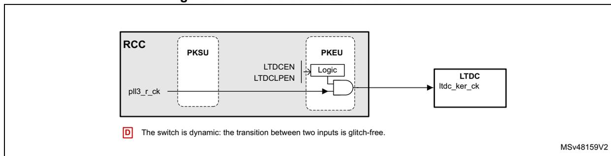
- 1. X represents the selected mux input after a system reset.
- 2. This figure does not show the connection of the bus interface clock to the peripheral. For details on each enable cell, refer to Section 8.5.11: Peripheral clock gating control .
The FMC, OCTOSPI1/2 and SDMMC1/2 can also use a clock different from the bus interface one for more flexibility.
Figure 60. Kernel clock distribution for SDMMC, OCTOSPI and FMC
![Figure 60: Kernel clock distribution for SDMMC, OCTOSPI and FMC. This block diagram shows the internal clocking logic for three peripherals. On the left, the RCC (Reset and Clock Control) block contains three multiplexers. The SDMMCSEL mux selects between pll1_q_ck (input 0) and pll2_r_ck (input 1). The OCTOSPISEL mux selects between rcc_hclk3 (0), pll1_q_ck (1), pll2_r_ck (2), and per_ck (3). The FMCSSEL mux also selects between rcc_hclk3 (0), pll1_q_ck (1), pll2_r_ck (2), and per_ck (3). These mux outputs pass through PKSU (Power Key Security Unit) and PKEU (Power Key Encryption Unit) blocks. Each path then enters a 'Logic' block that also receives enable signals (SDMMC[2:1]EN, SDMMC[2:1]LPEN, OCTOSPI[2:1]EN, OCTOSPI[2:1]LPEN, FMCPEN, FMCLPEN). The outputs of these logic blocks are the kernel clocks: sdmmc_ker_ck, octospi_ker_ck, and fmc_ker_ck, which are connected to the SDMMC1/2, OCTOSPI1/2, and FMC peripherals respectively. A note at the bottom left indicates that 'D' represents a dynamic switch that is glitch-free. The diagram is labeled MSV48160V2.](/RM0455-STM32H7A3-7B3-7B0/9e8a86180dc856005d4473bfbd5f13d9_img.jpg)
- 1. X represents the selected mux input after a system reset.
- 2. This figure does not show the connection of the bus interface clock to the peripheral. For details on each enable cell, refer to Section 8.5.11: Peripheral clock gating control .
Figure 61 shows the clock distribution for the USB blocks. The USB1ULPI block receives its clock from the external PHY.
The USB1OTG block receives two kind of clocks:
- • the clock for USB communications that can be selected among different sources thanks to the MUX controlled by USBSEL
- • the lsi_ck clock provided to the USB1OTG block in ADP mode on request.
Figure 61. Kernel clock distribution for USB (2)
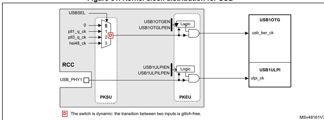
- 1. X represents the selected mux input after a system reset.
- 2. This figure does not show the connection of the bus interface clock to the peripheral. For details on each enable cell, refer to Section 8.5.11: Peripheral clock gating control .
Figure 62. Kernel clock distribution for ADCs, SWPMI, RNG and FDCANs
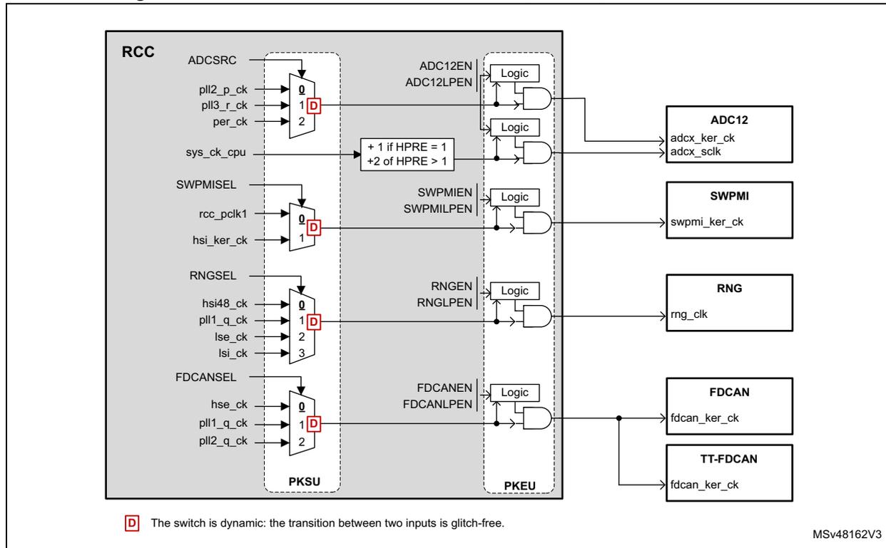
RCC
ADC SRC
pll2_p_ck
pll3_r_ck
per_ck
sys_ck_cpu
SWPMI SEL
rcc_pclk1
hsi_ker_ck
RNG SEL
hsi48_ck
pll1_q_ck
lse_ck
lsi_ck
FDCAN SEL
hse_ck
pll1_q_ck
pll2_q_ck
ADC12
adcx_ker_ck
adcx_selk
SWPMI
swpmi_ker_ck
RNG
rng_clk
FDCAN
fdcan_ker_ck
TT-FDCAN
fdcan_ker_ck
Logic
ADC12EN
ADC12LPEN
SWPMIEN
SWPMILPEN
RNGEN
RNGLPEN
FDCANEN
FDCANLPEN
PKSU
PKEU
+ 1 if HPRE = 1
+2 of HPRE > 1
D The switch is dynamic: the transition between two inputs is glitch-free.
MSV48162V3
- 1. X represents the selected mux input after a system reset.
- 2. This figure does not show the connection of the bus interface clock to the peripheral. For details on each enable cell, refer to Section 8.5.11: Peripheral clock gating control .
- 3. The ADC clock divider for the sys_ck_cpu do not need to be programmed but is set automatically depending on the HPRE (see also Figure 54: Core and bus clock generation ).
Figure 63. Kernel clock distribution for LPTIMs and HDMI-CEC (2)
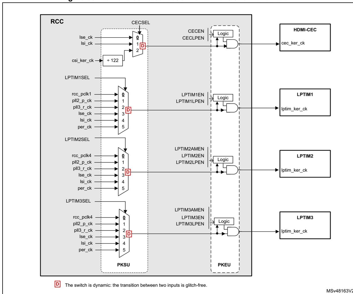
D The switch is dynamic: the transition between two inputs is glitch-free.
MSV48163V2
- 1. X represents the selected mux input after a system reset
- 2. This figure does not show the connection of the bus interface clock to the peripheral. For details on each enable cell, refer to Section 8.5.11: Peripheral clock gating control .
RTC/AWU clock
The rtc_ck clock source can be one of the following:
- • the hse_1M_ck ( hse_ck divided by a programmable prescaler)
- • the lse_ck
- • the lsi_ck clock
The source clock is selected by programming the RTCSEL[1:0] bits in the RCC Backup domain control register (RCC_BDCR) and the RTCPRE[5:0] bits in the RCC clock configuration register (RCC_CFGR) .
This selection cannot be modified without resetting the Backup domain.
If the LSE is selected as RTC clock, the RTC works normally even if the backup or the V DD supply disappears.
The LSE clock is in the Backup domain, whereas the other oscillators are not. As a consequence:
- • If LSE is selected as RTC clock, the RTC continues working even if the \( V_{DD} \) supply is switched OFF, provided the \( V_{BAT} \) supply is maintained.
- • If LSI is selected as the RTC clock, the AWU state is not guaranteed if the \( V_{DD} \) supply is powered off.
- • If the HSE clock is used as RTC clock, the RTC state is not guaranteed if the \( V_{DD} \) supply is powered off or if the \( V_{CORE} \) supply is powered off.
The rtc_ck clock is enabled through RTCEN bit located in the RCC Backup domain control register (RCC_BDCR) .
The RTC bus interface clock (APB clock) is enabled through RTCAPBEN and RTCAPBLPEN bits located in RCC_APB4ENR/LPENR registers.
Note: To read the RTC calendar register when the APB clock frequency is less than seven times the RTC clock frequency ( \( F_{APB} < 7 \times F_{RTCCLK} \) ), the software must read the calendar time and date registers twice. The data are correct if the second read access to RTC_TR gives the same result than the first one. Otherwise a third read access must be performed.
Watchdog clocks
The RCC provides the clock for the two watchdog blocks available on the circuit. The independent watchdog (IWDG) is connected to the LSI. The window watchdog (WWDG) is connected to the APB clock.
If an independent watchdog is started by either hardware option or software access, the LSI is forced ON and cannot be disabled. After the LSI oscillator setup delay, the clock is provided to the IWDG.
Clock frequency measurement using TIMx
Most of the clock source generator frequencies can be measured by means of the input capture of TIMx.
- • Calibrating the HSI or CSI with the LSE:
The primary purpose of having the LSE connected to a TIMx input capture is to be able to accurately measure the HSI or CSI. This requires to use the HSI or CSI as system clock source either directly or via PLL1. The number of system clock counts between consecutive edges of the LSE signal gives a measurement of the internal clock period. Taking advantage of the high precision of LSE crystals (typically a few tens of ppm) we can determine the internal clock frequency with the same resolution, and trim the source to compensate for manufacturing-process and/or temperature- and voltage-related frequency deviations.
The basic concept consists in providing a relative measurement (e.g. HSI/LSE ratio). The precision is therefore tightly linked to the ratio between the two clock sources. The greater the ratio is, the more accurate the measurement is.
The HSI and CSI oscillators have dedicated user-accessible calibration bits for this purpose (see RCC CSI calibration register (RCC_CSICFGR) ). When HSI or CSI is used via the PLLx, the system clock can also be fine-tuned by using the fractional divider of the PLLs.
- • Calibrating the LSI with the HSI:
The LSI frequency can also be measured: this is useful for applications that do not have a crystal. The ultra-low-power LSI oscillator has a large manufacturing process
deviation. The LSI clock frequency can be measured using the more precise HSI clock source. Using this measurement, a more accurate RTC time base timeouts (when LSI is used as the RTC clock source) and/or an IWDG timeout with an acceptable accuracy can be obtained.
8.5.9 General clock concept overview
The RCC handles the distribution of the CPU, bus interface and peripheral clocks for the system (CPU and SmartRun domains), according to the operating mode of each function (refer to Section 8.5.1: Clock naming convention for details on clock definitions).
For each peripheral, the application can control the activation/deactivation of its kernel and bus interface clock. Prior to use a peripheral, the CPU must enable it (by setting PERxEN to 1), and define if this peripheral remains active in CSleep mode (by setting PERxLPEN to 1). This is called 'allocation' of a peripheral to the CPU (refer to Section 8.5.10: Peripheral allocation for more details).
The peripheral allocation is used by the RCC to automatically control the clock gating according to the CPU and domain modes, and by the PWR to control the supply voltages of CPU and SmartRun domains.
Figure 64 gives an example of peripheral allocation: the CPU enables SDMMC1, SPI5 and AHBSRAM1. The AXISRAMs, ITCM, DTCM1, DTCM2 and SRDSRAM are implicitly allocated to the CPU. The group composed of the CPU, bus matrix 1/2/3 and allocated peripherals makes up a sub-system (CPU_SS).
Note: The FLASH, AXISRAMs, ITCM, DTCM1, DTCM2, SRDSRAM, IWDG, PWR, EXTI and RCC are common resources and are implicitly allocated to the CPU.
Figure 64. Peripheral allocation example
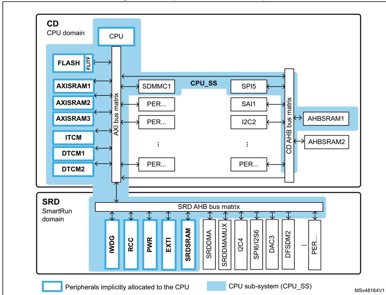
The diagram illustrates the peripheral allocation between the CPU domain (CD) and the SmartRun domain (SRD). The CD contains the CPU, FLASH, AXISRAM1, AXISRAM2, AXISRAM3, ITCM, DTCM1, and DTCM2. These are connected to an AXI bus matrix. The AXI bus matrix is connected to a CPU sub-system (CPU_SS) which includes SDMMC1, SPI5, SAI1, I2C2, and AHBSRAM1 and AHBSRAM2. The CPU_SS is connected to a CD AHB bus matrix. The SRD contains IWDG, RCC, PWR, EXTI, SRDSRAM, SRDMA, SRDMAMUX, I2C4, SPI6/I2S6, DAC3, DFSDM2, and various peripherals (PER...). These are connected to an SRD AHB bus matrix. The SRD AHB bus matrix is connected to the CD AHB bus matrix. A legend at the bottom indicates that white boxes represent peripherals implicitly allocated to the CPU, and blue boxes represent the CPU sub-system (CPU_SS). The reference MSV48164V1 is also shown.
Smart Run domain (SRD)
The SmartRun domain can be kept in DRun mode while the CPU is in CStop mode and the CPU domain is in DStop or DStop2 mode. This is done by setting RUN_SRD bit in PWR_CPUCR register.
- • If RUN_SRD is set to 1, then SmartRun domain is maintained in DRun mode, independently from the CPU modes (see power control, PWR_CPUCR register)
- • If RUN_SRD is set to 0, then the SmartRun domain enters DStop mode when the CPU enters CStop mode (see Table 59 ).
When the CPU domain enters CStop mode, the RCC automatically disables the bus interface and kernel clocks of all the peripherals of the CPU_SS, as well as the CPU clock. The PLLs, if enabled, are not disabled by the RCC since the SmartRun domain is still running.
The CPU can control if the CPU domain is allowed to enter DStop or Dstop2 modes or the SmartRun domain is allowed to enter in DStop when conditions are met, via bits RETDS_CD and PDDS_SRD of PWR control register (PWR_CPUCR).
A wake-up event is able to exit the CPU domain from DStop or Dstop2 and the SmartRun domain from DStop mode.
Autonomous mode
The Autonomous mode allows the delivery of the clocks to peripherals located in the SmartRun domain, even if the CPU is in CStop mode. When a peripheral has its autonomous bit activated, it receives its peripheral clocks according to the SmartRun domain state, if the CPU is in CStop mode:
- • If the SmartRun domain is in DRun mode, peripherals with Autonomous mode activated receive their peripheral clocks,
- • If the SmartRun domain is in DStop mode, no peripheral clock is provided.
The Autonomous mode does not prevent the SmartRun domain to enter DStop or DStop2 mode.
The autonomous bits are located in RCC SmartRun domain Autonomous mode register (RCC_SRDAMR) .
For example, the CPU can enter CStop mode while the I2S6 is filling the SRDSRAM with data received from an external device via BDMA2. When the amount of received data is reached, the CPU can be re-activated by a wake-up event. This can be done by setting the I2S6, the BDMA2, and SRDSRAM in Autonomous mode, while keeping the SmartRun domain in DRun mode (RUN_SRD set to 1). In this example, the RCC does not switch off the PLLs as the SmartRun domain is always in DRun mode.
It is possible to go a step further with power-consumption reduction by combining the Autonomous mode with the capability of some peripherals (UARTs, I2Cs) to request the kernel clock on their own, without waking-up the CPU. For example, if the system is expecting messages via I2C4, the whole system can be put in Stop mode. When the I2C4 peripheral detects a START bit, it generates a “kernel clock request”. This request enables the HSI or CSI, and a kernel clock is provided only to the requester (in our example the I2C4). The I2C4 then decodes the incoming message.
Several cases are then possible:
- • If the device address of the message does not match, then I2C4 releases its “kernel clock request” until a new START condition is detected.
- • If the device address of the incoming message matches, it must be stored into the SmartRun local memory. I2C4 is able to generate a wake-up event on address match to switch the SmartRun domain to DRun mode. The message is then transferred into memory via BDMA2, and the SmartRun domain go back to DStop mode without any CPU activation. Note that if the amount of data transferred into memory reached the transfer count, the BDMA2 can also generate an interrupt to wake-up the CPU.
- • If the device address of the incoming message matches and the peripheral is setup to wake up the CPU, then I2C4 generates a wake-up event to activate the CPU.
Refer to the description of EXTI block to see which peripheral is able to perform a wake-up event to which domain.
Memory handling
The CPU can access all the memory areas available in the product:
- • AXISRAM1, AXISRAM2, AXISRAM3, ITCM, DTCM1, DTCM2 and FLASH
- • AHBSRAM1 and AHBSRAM2
- • SRDSRAM and BKPRAM
As shown in Figure 64 , FLASH, AXISRAMs, SRDSRAM, ITCM, DTCM1 and DTCM2 are implicitly allocated to the CPU. As a result, there is no enable bit allowing the CPU to allocate these memories.
The BKPRAM has a dedicated enable in order to gate the bus interface clock. The CPU needs to enable the BKPRAM prior to use it.
Note: The memory interface clocks (flash memory and RAM interfaces) can be stopped by software during CSleep mode (via SRAMyLPEN bits).
Refer to Section 8.5.11: Peripheral clock gating control and Section 8.5.12: CPU and bus matrix clock gating control sections for details on clock enabling.
System states overview
Table 59 gives an overview of the system states with respect to the CPU and SmartRun domain modes.
- • The system remains in Run mode as long as the SmartRun domain is in DRun mode. Several sub-states of system Run exist that are not detailed here (refer Section 6: Power control (PWR) for more information).
- • The SmartRun domain can run while the CPU domain is in DStop or DStop2 mode thanks to RUN_SRD bits of PWR_CPUCR registers or when the SmartRun domain is in Autonomous mode.
- • The system remains in Stop mode as long as the SmartRun domain is in DStop mode. This means implicitly that the CPU domain is in DStop or DStop2 mode. As soon as the CPU domain exits DStop or DStop2, the SmartRun domain switches to DRun mode.
- • The system remains in Standby mode as long as CPU and SmartRun domains are in DStandby.
- • Domain states versus CPU states:
- – When the CPU domain is in DRun mode, it means that its bus matrix is clocked and the CPU is in CRun mode.
- – When the CPU domain is in DStop mode, it means that its bus matrix is no longer clocked and the CPU is in CStop mode.
- – When a domain is in DStandby mode, it means that the domain including its CPU are powered down.
Table 59. System states overview
| System state | CPU domain state | SmartRun domain state |
|---|---|---|
| Run | DRun | DRun |
| Autonomous | DStop/DStop2 | |
| Stop | DStop/DStop2 | DStop |
| Standby | DStandby | DStandby |
8.5.10 Peripheral allocation
The CPU can allocate a peripheral and hence control its kernel and bus interface clock.
The CPU can allocate a peripheral by setting the dedicated PERxEN bit located into the RCC_XXXXENR registers.
The CPU can control the peripheral clocks gating when it is in CSleep mode via the PERxLPEN bits located into the RCC_XXXXLPENR registers.
Refer to RCC source control register (RCC_CR) for additional information.
The peripheral allocation bits (PERxEN bits) are used by the hardware to provide the kernel and bus interface clocks to the peripherals. However they are also used to link peripherals to the CPU (CPU sub-system). In this way, the hardware is able to safely gate the peripheral clocks and bus matrix clocks according to CPU states. The PWR block also uses this information to control properly the domain states.
Clock switches and gating
- Clock switching delays
The input selected by the kernel clock switches can be changed dynamically without generating spurs or timing violation. As a consequence, switching from the original to the new input can only be performed if a clock is present on both inputs. If it is not the case, no clock is provided to the peripheral. To recover from this situation, the user must provide a valid clock to both inputs.
During the transition from one input to another, the kernel clock provided to the peripheral is gated, in the worst case, during 2 clock cycles of the previously selected clock, and 2 clock cycles of the new selected clock. As shown in Figure 65 , both input clocks must be present during transition time.
Figure 65. Kernel clock switching
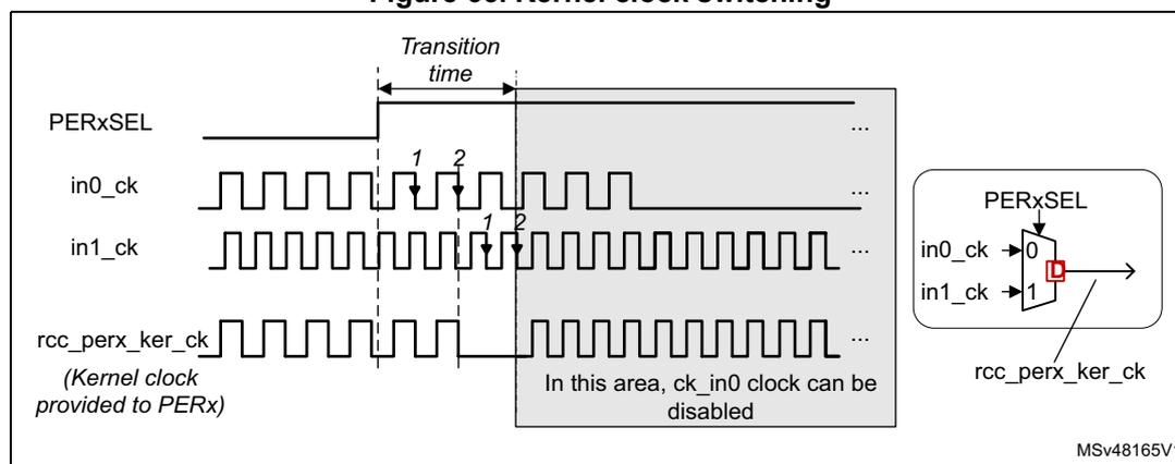
The diagram illustrates the timing and logic for kernel clock switching. On the left, a timing diagram shows the transition of the PERxSEL signal. When PERxSEL changes, the selected clock (in0_ck or in1_ck) is gated. The rcc_perx_ker_ck signal is shown as a continuous clock. The transition time is marked, and the diagram indicates that both input clocks must be present during the transition. On the right, a logic schematic shows a multiplexer (PERxSEL) selecting between in0_ck and in1_ck to provide the rcc_perx_ker_ck signal. The text 'In this area, ck_in0 clock can be disabled' is present in the timing diagram.
- Clock enabling delays
In the same way, the clock gating logic synchronizes the enable command (coming generally from a kernel clock request or PERxEN bits) with the selected clock, in order to avoid generation of spurs.
- – A maximum delay of two periods of the enabled clock may occur between the enable command and the first rising edge of the clock. The enable command can
be the rising edge of the PERxEN bits of RCC_XXXXENR registers, or a kernel clock request asserted by a peripheral.
- – A maximum delay of 1.5 periods of the disabled clock may occur between the disable command and the last falling edge of the clock. The disable command can be the falling edge of the PERxEN bits of RCC_XXXXENR registers, or a kernel clock request released by a peripheral.
Note: Both the kernel and bus interface clocks are affected by this re-synchronization delay.
8.5.11 Peripheral clock gating control
As mentioned previously, each peripheral requires a bus interface clock, named rcc_perx_bus_ck (for peripheral 'x'). This clock can be an APB, AHB or AXI clock, according to which bus the peripheral is connected.
The clocks used as bus interface for peripherals located in the CPU domain, can be rcc_aclk , rcc_hclk3 or rcc_pclk3 , depending on the bus connected to each peripheral. For simplicity sake, these clocks are named rcc_bus_cd_ck .
Similarly, the signal rcc_bus_srd_ck represents rcc_hclk4 or rcc_pclk4 for peripherals located in the SmartRun domain.
Some peripherals (such as SAI or UART) also require a dedicated clock for their communication interface. This clock is generally asynchronous with respect to the bus interface clock. It is named kernel clock ( perx_ker_ckreq ). Both clocks can be gated according to several conditions detailed hereafter.
As shown in Figure 66 , enabling the kernel and bus interface clocks of each peripheral depends on several input signals:
- • PERxEN and PERxLPEN bits,
PERxEN represents the peripheral enable (allocation) bit for the CPU. The CPU can write these bits to 1 via the RCC_XXXXENR registers. - • PERxAMEN bits belonging to RCC SmartRun domain Autonomous mode register (RCC_SRDAMR) .
- • CPU state ( cpu_sleep and cpu_deep sleep signals)
- • SmartRun domain state ( srd_deep sleep signal)
- • Kernel clock request ( perx_ker_ckreq ) of the peripheral itself, when the feature is available
Refer to Section 8.5.10: Peripheral allocation for more details.
Figure 66. Peripheral kernel clock enable logic details
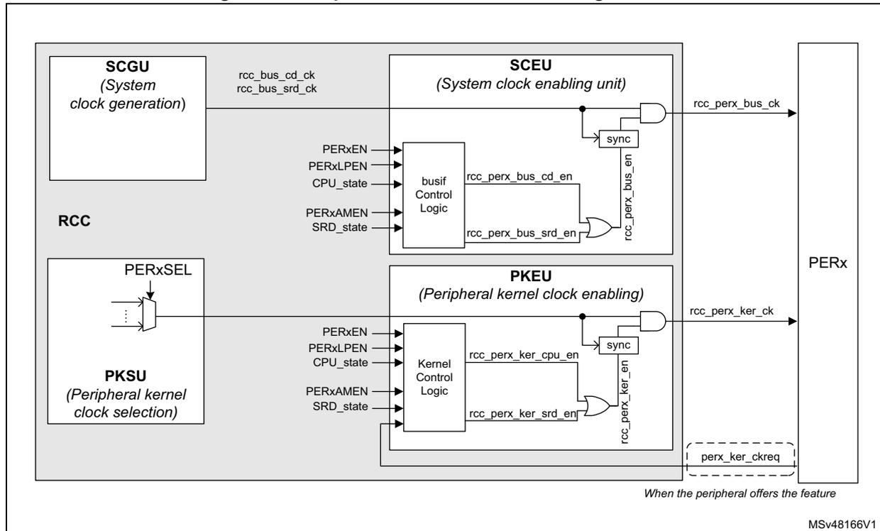
Table 60 gives a detailed description of the enabling logic of the peripheral clocks for peripherals located in the CPU domain and allocated by the CPU.
Table 60. Peripheral clock enabling for the CPU domain peripherals
| PERxEN | PERxLPEN | PERxSEL | perx_ker_ckreq | CPU state | rcc_perx_ker_cpu_en | rcc_perx_bus_cd_en | Comments |
|---|---|---|---|---|---|---|---|
| 0 | X | X | X | X | 0 | 0 | No clock provided to the peripheral, because PERxEN=0 |
| 1 | X | X | X | CRun | 1 | 1 | Kernel and bus interface clocks are provided to the peripheral, because the CPU is in CRun, and PERxEN = 1. |
| 1 | 0 | X | X | CSleep | 0 | 0 | No clock provided to the peripheral, because the CPU is in CSleep and PERxLPEN = 0 |
| 1 | 1 | X | X | CSleep | 1 | 1 | Kernel and bus interface clocks are provided to the peripheral, because CPU is in CSleep, and PERxLPEN = 1 |
Table 60. Peripheral clock enabling for the CPU domain peripherals (continued)
| PERxEN | PERxLPEN | PERxSEL | perx_ker_ckreq | CPU state | rcc_perx_ker_cpu_en | rcc_perx_bus_cd_en | Comments |
|---|---|---|---|---|---|---|---|
| 1 | 0 | X | X | 0 | 0 | No clock provided to the peripheral because the PERxLPEN bit is set to 0. | |
| 1 | 1 | no lsi_ck and no lse_ck and no hsi_ker_ck and no csi_ker_ck | X | CStop | 0 | 0 | No clock provided to the peripheral because CPU is in CStop and lse_ck or lsi_ck or hsi_ker_ck or csi_ker_ck are not selected. |
| 1 | 1 | lsi_ck or lse_ck | X | 1 (1) | 0 | Kernel clock is provided to the peripheral because PERxEN = PERxLPEN = 1 and
lsi_ck
or
lse_ck
are selected. The bus interface clock is no provided as the CPU is in CStop. | |
| 1 | 1 | hsi_ker_ck or csi_ker_ck | 1 | 1 | 0 | Kernel clock is provided to the peripheral because
req_ker_perx
= 1, and PERxEN = PERxLPEN = 1 and
hsi_ker_ck
or
csi_ker_ck
are selected. The bus interface clock is no provided as the CPU is in CStop. | |
| 1 | 1 | hsi_ker_ck or csi_ker_ck | 0 | 0 | 0 | No clock provided to the peripheral because CPU is in CStop, and no kernel clock request pending |
- 1. For RNG block, the kernel clock is not delivered if the CPU to which it is allocated is in CStop mode, even if the clock selected is lsi_ck or lse_ck .
As a summary, we can state that the kernel clock is provided to the peripherals located on the CPU domain when the following conditions are met:
- 1. The CPU is in CRun mode, and the peripheral is allocated.
- 2. The CPU is in CSleep mode and the peripheral is allocated with PERxLPEN = 1.
- 3. The CPU is in CStop mode, the peripheral is allocated with PERxLPEN = 1, the peripheral generates a kernel clock request and the selected clock is hsi_ker_ck or csi_ker_ck .
- 4. The CPU is in CStop mode, the peripheral is allocated with PERxLPEN = 1 and the kernel source clock of the peripheral is lse_ck or lsi_ck .
The bus interface clock is provided to the peripherals only when conditions 1 or 2 are met.
Table 61 gives a detailed description of the enabling logic of the kernel clock for all peripherals located in the SmartRun domain.
Table 61. Peripheral clock enabling for SmartRun domain peripherals
| PERxEN | PERxLPEN | PERxAMEN | PERxSEL | perx_ker_ckreq | CPU state | SmartRun domain state | rcc_perx_ker_srd_en | rcc_perx_bus_srd_en | Comments |
|---|---|---|---|---|---|---|---|---|---|
| 0 | X | X | X | X | Any | Any | 0 | 0 | No clock provided to the peripheral, as PERxEN = 0 |
| 1 | X | X | X | X | CRun | Run | 1 | 1 | Kernel and bus interface clocks are provided to the peripheral, because the CPU is in CRun, and PERxEN = 1. |
| 1 | 0 | X | X | X | CSleep | 0 | 0 | No clock provided to the peripheral, because the CPU is in CSleep, and PERxLPEN = 0 | |
| 1 | 1 | X | X | X | 1 | 1 | Kernel and bus interface clocks are provided to the peripheral, because the CPU is in CSleep, and PERxLPEN = 1 | ||
| 1 | X | 0 | X | X | 0 | 0 | As the CPU is in CStop, and PERxEN=1, then the kernel clock gating depends on the SmartRun domain state and PERxAMEN bits. No clock provided to the peripheral because PERxAMEN = 0. | ||
| 1 | X | 1 | X | X | CStop | 1 | 1 | The kernel and bus interface clocks are provided because even if the CPU is in CStop mode, the SmartRun domain is in Run mode, with PERxEN and PERxAMEN bits set to 1. | |
| 1 | X | 1 | not lse_ck and not lsi_ck | 0 | Stop | 0 | 0 | No clock provided to the peripheral, because the SmartRun domain is in Stop, req_ker_perx = 0, and lse_ck or lsi_ck is not selected | |
Table 61. Peripheral clock enabling for SmartRun domain peripherals (continued)
| PERxEN | PERxLPEN | PERxAMEN | PERxSEL | perx_ker_ckreq | CPU state | SmartRun domain state | rcc_perx_ker_srd_en | rcc_perx_bus_srd_en | Comments |
|---|---|---|---|---|---|---|---|---|---|
| 1 | X | 1 | not hsi_ker_ck and not csi_ker_ck and not lse_ck and not lsi_ck | 1 | 0 | 0 | No clock provided to the peripheral, because even if req_ker_perx = 0, lse_ck or lsi_ck or hsi_ker_ck or csi_ker_ck is not selected. | ||
| 1 | X | 1 | hsi_ker_ck or csi_ker_ck | 1 | 1 | 0 | Kernel clock is provided to the peripheral because req_ker_perx = 1, and PERxEN = PERxAMEN = 1, and the selected clock is hsi_ker_ck or csi_ker_ck . The bus interface clock is not provided as the SmartRun domain is in Stop. | ||
| 1 | X | 1 | lse_ck or lsi_ck | X | 1 | 0 | Kernel clock is provided to the peripheral because PERxEN = PERxAMEN = 1 and lse_ck or lsi_ck are selected, while the SmartRun domain is in Stop. The bus interface clock is not provided as the SmartRun domain is in Stop. |
As a summary, we can state that the kernel clock is provided to the peripherals of the SmartRun domain if the following conditions are met:
- 1. The CPU is in CRun mode and the peripheral is allocated.
- 2. The CPU is in CSleep mode and the peripheral is allocated with PERxLPEN = 1.
- 3. The CPU is in CStop mode, the peripheral is allocated and the SmartRun domain is in Run mode with PERxAMEN = 1.
- 4. The CPU is in CStop mode, the peripheral is allocated, the SmartRun domain is in Stop mode with PERxAMEN = 1, the peripheral is generating a kernel clock request and the kernel clock source is hsi_ker_ck or csi_ker_ck .
- 5. The CPU is in CStop mode, the peripheral is allocated, the SmartRun domain is in Stop mode with PERxAMEN = 1 and the kernel clock source of the peripheral is lse_ck or lsi_ck .
The bus interface clock is provided to the peripherals only when condition 1, 2 or 3 is met.
Note: When they are set to 1, the autonomous bits indicate that the associated peripheral receives a kernel clock according to the SmartRun domain state and not according to the mode of the CPU.
Only I2C, U(S)ART and LPUART peripherals are able to request the kernel clock. This feature gives to the peripheral the capability to transfer data with an optimal power consumption.
The autonomous bits dedicated to some peripherals located in the SmartRun domain, allow the data transfer with external devices without activating the CPU.
In order for the LPTIMER to operate with Ise_ck or Isi_ck when the circuit is in Stop mode, the user application must select the Isi_ck or Ise_ck input via LPTIMxSEL fields, and set LPTIMxAMEN and LPTIMxLPEN bits to 1.
8.5.12 CPU and bus matrix clock gating control
For each domain it is possible to control the activation/deactivation of the CPU clock and bus matrix clock.
For information about convention naming, refer to Section 8.5.11: Peripheral clock gating control .
The clocks of the CPU, AHB and AXI bridges and APB busses are enabled according to the rules hereafter:
- • The CPU clock rcc_cpu_ck is enabled when the CPU is in CRun mode.
- • The AXI bridge clock is enabled when the CPU domain is in DRun mode.
- • Each AXI master and slave has an independent clock gating that can be activated to further reduce the power consumption (register RCC_CKGAENR). When activated the clock is automatically enabled on bus transaction request.
- • The CPU domain AHB bridges clocks are enabled when the CPU domain is in DRun mode.
- • The SmartRun domain AHB bridge clock is enabled when one of the following conditions is met:
- – The CPU is in CRun or CSleep mode.
- – When the RUN_SRD bit is set to 1, independently of CPU modes.
- – When the SRD_deep sleep signal is inactive (0), independently of CPU modes.
- • The APB1,2,3 busses are enabled when one of the following conditions is met:
- – The CPU is in CRun mode.
- – When the CPU is in CSleep mode with at least one peripheral connected to this bus having both its PERxEN and PERxLPEN set to 1.
- • The APB4 bus is enabled when the SmartRun domain is in DRun mode.
As shown in the Figure 67 , the enabling of the core and bus clock of each domain depends on several input signals:
- • cpu_sleep and cpu_deep sleep signals from the CPU
- • srd_sleepdeep signal
- • RCC_xxxENR.PERxEN bits of peripherals located on the CPU domain
Figure 67. Bus clock enable logic
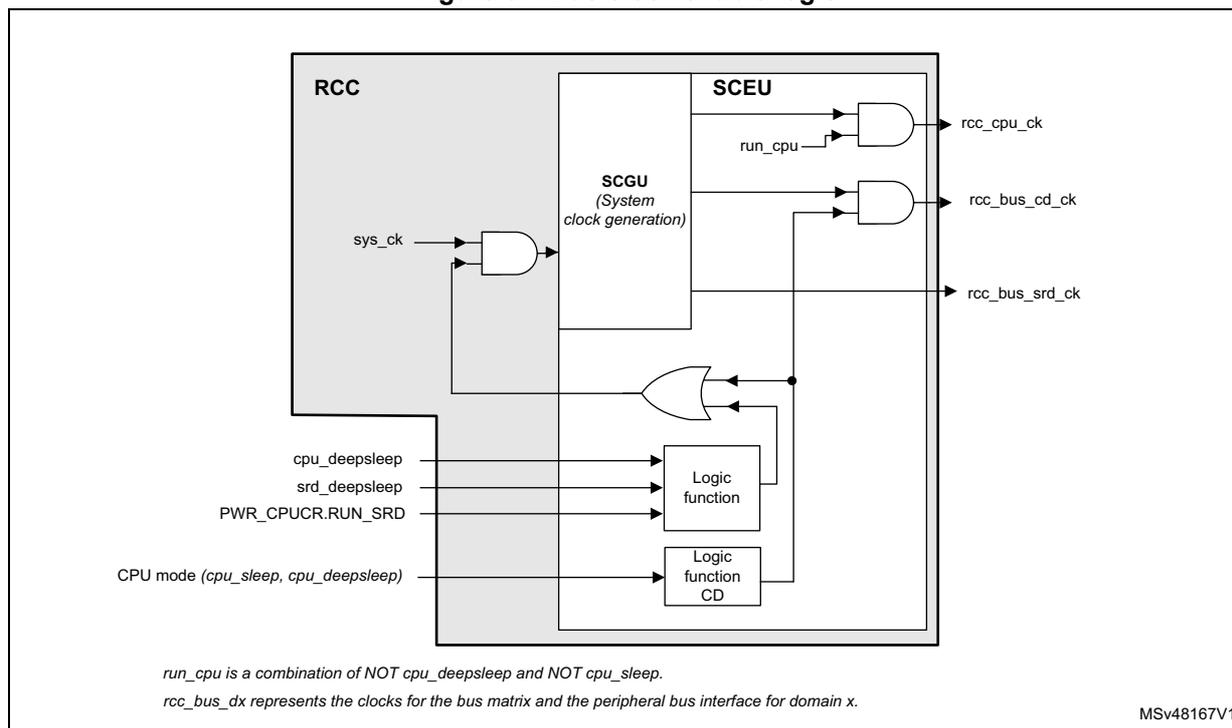
run_cpu is a combination of NOT cpu_deepsleep and NOT cpu_sleep.
rcc_bus_dx represents the clocks for the bus matrix and the peripheral bus interface for domain x.
MSV48167V1
8.6 RCC interrupts
The RCC provides three interrupt lines:
- • rcc_it : general interrupt line providing events when the PLLs are ready or when the oscillators are ready
- • rcc_hsecss_it : interrupt line dedicated to the failure detection of the HSE CSS (clock security system)
- • rcc_lsecss_it : interrupt line dedicated to the failure detection of the LSE CSS
The interrupt enable is controlled via RCC clock source interrupt enable register (RCC_CIER) , except for the HSE CSS failure. When the HSE CSS feature is enabled, it is not possible to mask the interrupt generation.
The interrupt flags can be checked via RCC clock source interrupt flag register (RCC_CIFR) , and those flags can be cleared via RCC clock source interrupt clear register (RCC_CICR) .
Note: The interrupt flags are not relevant if the corresponding interrupt enable bit is not set.
Table 62 gives a summary of the interrupt sources and the way to control them.
Table 62. Interrupt sources and control
| Interrupt source | Description | Interrupt enable | Action to clear interrupt | Interrupt line |
|---|---|---|---|---|
| LSIRDYF | LSI ready | LSIRDYIE | Set LSIRDYC to 1 | rcc_it |
| LSERDYF | LSE ready | LSERDYIE | Set LSERDYC to 1 | |
| HSIDRYF | HSI ready | HSIDRYIE | Set HSIRDYC to 1 | |
| HSERDYF | HSE ready | HSERDYIE | Set HSERDYC to 1 | |
| CSIRDYF | CSI ready | CSIRDYIE | Set CSIRDYC to 1 | |
| HSI48RDYF | HSI48 ready | HSI48RDYIE | Set HSI48RDYC to 1 | |
| PLL1RDYF | PLL1 ready | PLL1RDYIE | Set PLL1RDYC to 1 | |
| PLL2RDYF | PLL2 ready | PLL2RDYIE | Set PLL2RDYC to 1 | |
| PLL3RDYF | PLL3 ready | PLL3RDYIE | Set PLL3RDYC to 1 | |
| LSECSSF | LSE CSS failure | LSECSSFIE (1) | Set LSECSSC to 1 | rcc_lsecss_it |
| HSECSSF | HSE CSS failure | _ (2) | Set HSECSSC to 1 | rcc_hsecss_it |
- 1. The security system feature must also be enabled (LSECSSON = 1), in order to generate interrupts.
2. It is not possible to mask this interrupt when the security system feature is enabled (HSECSSON = 1).
8.7 RCC registers
8.7.1 RCC source control register (RCC_CR)
Address offset: 0x000
Reset value: 0x0000 0025
| 31 | 30 | 29 | 28 | 27 | 26 | 25 | 24 | 23 | 22 | 21 | 20 | 19 | 18 | 17 | 16 |
|---|---|---|---|---|---|---|---|---|---|---|---|---|---|---|---|
| Res. | Res. | PLL3RDY | PLL3ON | PLL2RDY | PLL2ON | PLL1RDY | PLL1ON | Res. | Res. | Res. | HSEEXT | HSECSSON | HSEBYP | HSERDY | HSEON |
| r | rw | r | rw | r | rw | rw | rs | rw | r | rw |
| 15 | 14 | 13 | 12 | 11 | 10 | 9 | 8 | 7 | 6 | 5 | 4 3 | 2 | 1 | 0 | |
|---|---|---|---|---|---|---|---|---|---|---|---|---|---|---|---|
| CDCKRDY | CPUCKRDY | HSI48RDY | HSI48ON | Res. | Res. | CSIKERON | CSIRDY | CSION | Res. | HSIDIVF | HSIDIV[1:0] | HSIRDY | HSIKERON | HSION | |
| r | r | r | rw | rw | r | rw | r | rw | r | rw | rw | ||||
Bits 31:30 Reserved, must be kept at reset value.
Bit 29 PLL3RDY : PLL3 clock ready flag
Set by hardware to indicate that the PLL3 is locked.
0: PLL3 unlocked (default after reset)
1: PLL3 locked
Bit 28 PLL3ON : PLL3 enable
Set and cleared by software to enable PLL3.
Cleared by hardware when entering Stop or Standby mode.
0: PLL3 OFF (default after reset)
1: PLL3 ON
Bit 27 PLL2RDY : PLL2 clock ready flag
Set by hardware to indicate that the PLL2 is locked.
0: PLL2 unlocked (default after reset)
1: PLL2 locked
Bit 26 PLL2ON : PLL2 enable
Set and cleared by software to enable PLL2.
Cleared by hardware when entering Stop or Standby mode.
0: PLL2 OFF (default after reset)
1: PLL2 ON
Bit 25 PLL1RDY : PLL1 clock ready flag
Set by hardware to indicate that the PLL1 is locked.
0: PLL1 unlocked (default after reset)
1: PLL1 locked
Bit 24 PLL1ON : PLL1 enable
Set and cleared by software to enable PLL1.
Cleared by hardware when entering Stop or Standby mode. Note that the hardware prevents writing this bit to 0, if the PLL1 output is used as the system clock.
0: PLL1 OFF (default after reset)
1: PLL1 ON
Bits 23:21 Reserved, must be kept at reset value.
Bit 20 HSEEXT : external high speed clock type in Bypass mode
Set and reset by software to select the external clock type (analog or digital).
The external clock must be enabled with the HSEON bit to be used by the device.
The HSEEXT bit can be written only if the HSE oscillator is disabled.
0: HSE in analog mode (default after reset)
1: HSE in digital mode
Bit 19 HSECSSON : HSE clock security system enable
Set by software to enable clock security system on HSE.
This bit is “set only” (disabled by a system reset or when the system enters in Standby mode).
When HSECSSON is set, the clock detector is enabled by hardware when the HSE is ready and disabled by hardware if an oscillator failure is detected.
0: CSS on HSE OFF (clock detector OFF) (default after reset)
1: CSS on HSE ON (clock detector ON if the HSE oscillator is stable, OFF if not).
Bit 18 HSEBYP: HSE clock bypassSet and cleared by software to bypass the oscillator with an external clock. The external clock must be enabled with the HSEON bit to be used by the device.
The HSEBYP bit can be written only if the HSE oscillator is disabled.
0: HSE oscillator not bypassed (default after reset)
1: HSE oscillator bypassed with an external clock
Bit 17 HSERDY: HSE clock ready flagSet by hardware to indicate that the HSE oscillator is stable.
0: HSE clock is not ready (default after reset)
1: HSE clock is ready
Bit 16 HSEON: HSE clock enableSet and cleared by software.
Cleared by hardware to stop the HSE when entering Stop or Standby mode.
This bit cannot be cleared if the HSE is used directly (via SW mux) as system clock, or if the HSE is selected as reference clock for PLL1 with PLL1 enabled (PLL1ON bit set to 1).
0: HSE is OFF (default after reset)
1: HSE is ON
Bit 15 CDCKRDY: CPU domain clocks ready flagSet by hardware to indicate that the following CPU domain clocks are available: APB1, APB2, AHB bus matrix.
0: CPU domain clocks are not available (default after reset)
1: CPU domain clocks are available
Bit 14 CPUCKRDY: CPU related clocks ready flagSet by hardware to indicate that the CPU related clocks (CPU, APB3, AXI bus matrix and related memories) are available.
0: CPU related clocks are not available (default after reset)
1: CPU related clocks are available
Bit 13 HSI48RDY: HSI48 clock ready flagSet by hardware to indicate that the HSI48 oscillator is stable.
0: HSI48 clock is not ready (default after reset)
1: HSI48 clock is ready
Bit 12 HSI48ON: HSI48 clock enableSet by software and cleared by software or by the hardware when the system enters to Stop or Standby mode.
0: HSI48 is OFF (default after reset)
1: HSI48 is ON
Bits 11:10 Reserved, must be kept at reset value.
Bit 9 CSIKERON: CSI clock enable in Stop modeSet and reset by software to force the CSI to ON, even in Stop mode, in order to be quickly available as kernel clock for some peripherals. This bit has no effect on the value of CSION.
0: no effect on CSI (default after reset)
1: CSI is forced to ON even in Stop mode
Bit 8 CSIRDY: CSI clock ready flagSet by hardware to indicate that the CSI oscillator is stable. This bit is activated only if the RC is enabled by CSION (it is not activated if the CSI is enabled by CSIKERON or by a peripheral request).
0: CSI clock is not ready (default after reset)
1: CSI clock is ready
Bit 7 CSION: CSI clock enableSet and reset by software to enable/disable CSI clock for system and/or peripheral.
Set by hardware to force the CSI to ON when the system leaves Stop mode, if STOPWUCK = 1 or STOPKERWUCK = 1.
This bit cannot be cleared if the CSI is used directly (via SW mux) as system clock, or if the CSI is selected as reference clock for PLL1 with PLL1 enabled (PLL1ON bit set to 1).
0: CSI is OFF (default after reset)
1: CSI is ON
Bit 6 Reserved, must be kept at reset value. Bit 5 HSIDIVF: HSI divider flagSet and reset by hardware.
As a write operation to HSIDIV has not an immediate effect on the frequency, this flag indicates the current status of the HSI divider. HSIDIVF goes immediately to 0 when HSIDIV value is changed, and is set back to 1 when the output frequency matches the value programmed into HSIDIV.
0: new division ratio not yet propagated to hsi(_ker)_ck (default after reset)
1: hsi(_ker)_ck clock frequency reflects the new HSIDIV value (default register value when the clock setting is completed)
Bits 4:3 HSIDIV[1:0]: HSI clock dividerSet and reset by software.
These bits allow selecting a division ratio in order to configure the wanted HSI clock frequency. The HSIDIV cannot be changed if the HSI is selected as reference clock for at least one enabled PLL (PLLxON bit set to 1). In that case, the new HSIDIV value is ignored.
00: division by 1, hsi(_ker)_ck = 64 MHz (default after reset)
01: division by 2, hsi(_ker)_ck = 32 MHz
10: division by 4, hsi(_ker)_ck = 16 MHz
11: division by 8, hsi(_ker)_ck = 8 MHz
Bit 2 HSIRDY: HSI clock ready flagSet by hardware to indicate that the HSI oscillator is stable.
0: HSI clock is not ready (default after reset)
1: HSI clock is ready
Bit 1 HSIKERON: HSI clock enable in Stop modeSet and reset by software to force the HSI to ON, even in Stop mode, in order to be quickly available as kernel clock for peripherals. This bit has no effect on the value of HSION.
0: no effect on HSI (default after reset)
1: HSI is forced to ON even in Stop mode
Bit 0 HSION: HSI clock enableSet and cleared by software.
Set by hardware to force the HSI to ON when the product leaves Stop mode, if STOPWUCK = 0 or STOPKERWUCK = 0.
Set by hardware to force the HSI to ON when the product leaves Standby mode or in case of a failure of the HSE which is used as the system clock source.
This bit cannot be cleared if the HSI is used directly (via SW mux) as system clock, or if the HSI is selected as reference clock for PLL1 with PLL1 enabled (PLL1ON bit set to 1).
0: HSI is OFF
1: HSI is ON (default after reset)
8.7.2 RCC HSI calibration register (RCC_HSICFGR)
Address offset: 0x004
Reset value: 0x4000 0XXX
Reset value depends on the flash option bytes setting.
| 31 | 30 | 29 | 28 | 27 | 26 | 25 | 24 | 23 | 22 | 21 | 20 | 19 | 18 | 17 | 16 |
|---|---|---|---|---|---|---|---|---|---|---|---|---|---|---|---|
| Res. | HSITRIM[6:0] | Res. | Res. | Res. | Res. | Res. | Res. | Res. | Res. | ||||||
| rw | rw | rw | rw | rw | rw | rw | |||||||||
| 15 | 14 | 13 | 12 | 11 | 10 | 9 | 8 | 7 | 6 | 5 | 4 | 3 | 2 | 1 | 0 |
| Res. | Res. | Res. | Res. | HSICAL[11:0] | |||||||||||
| r | r | r | r | r | r | r | r | r | r | r | r | ||||
Bit 31 Reserved, must be kept at reset value.
Bits 30:24 HSITRIM[6:0] : HSI clock trimming
Set by software to adjust calibration.
HSITRIM field is added to the engineering option bytes loaded during reset phase
(FLASH_HSI_opt) in order to form the calibration trimming value.
HSICAL = HSITRIM + FLASH_HSI_opt.
Note: The reset value of the field is 0x40.
Bits 23:12 Reserved, must be kept at reset value.
Bits 11:0 HSICAL[11:0] : HSI clock calibration
Set by hardware by option byte loading during system reset nreset .
Adjusted by software through trimming bits HSITRIM.
This field represents the sum of engineering option byte calibration value and HSITRIM bits value.
8.7.3 RCC clock recovery RC register (RCC_CRRRCR)
Address offset: 0x008
Reset value: 0x0000 0XXX
Reset value depends on the flash option bytes setting.
| 31 | 30 | 29 | 28 | 27 | 26 | 25 | 24 | 23 | 22 | 21 | 20 | 19 | 18 | 17 | 16 |
|---|---|---|---|---|---|---|---|---|---|---|---|---|---|---|---|
| Res. | Res. | Res. | Res. | Res. | Res. | Res. | Res. | Res. | Res. | Res. | Res. | Res. | Res. | Res. | Res. |
| 15 | 14 | 13 | 12 | 11 | 10 | 9 | 8 | 7 | 6 | 5 | 4 | 3 | 2 | 1 | 0 |
| Res. | Res. | Res. | Res. | Res. | Res. | HSI48CAL[9:0] | |||||||||
| r | r | r | r | r | r | r | r | r | r | ||||||
Bits 31:10 Reserved, must be kept at reset value.
Bits 9:0 HSI48CAL[9:0] : Internal RC 48 MHz clock calibration
Set by hardware by option byte loading during system reset nreset .
Read-only.
8.7.4 RCC CSI calibration register (RCC_CSICFGR)
Address offset: 0x00C
Reset value: 0x2000 0XXX
Reset value depends on the flash option bytes setting.
| 31 | 30 | 29 | 28 | 27 | 26 | 25 | 24 | 23 | 22 | 21 | 20 | 19 | 18 | 17 | 16 |
|---|---|---|---|---|---|---|---|---|---|---|---|---|---|---|---|
| Res. | Res. | CSITRIM[5:0] | Res. | Res. | Res. | Res. | Res. | Res. | Res. | Res. | |||||
| rw | rw | rw | rw | rw | rw | ||||||||||
| 15 | 14 | 13 | 12 | 11 | 10 | 9 | 8 | 7 | 6 | 5 | 4 | 3 | 2 | 1 | 0 |
|---|---|---|---|---|---|---|---|---|---|---|---|---|---|---|---|
| Res. | Res. | Res. | Res. | Res. | Res. | Res. | Res. | CSICAL[7:0] | |||||||
| r | r | r | r | r | r | r | r | ||||||||
Bits 31:30 Reserved, must be kept at reset value.
Bits 29:24 CSITRIM[5:0] : CSI clock trimming
Set by software to adjust calibration.
CSITRIM field is added to the engineering option bytes loaded during reset phase (FLASH_CSI_opt) in order to form the calibration trimming value.
CSICAL = CSITRIM + FLASH_CSI_opt.
Note: The reset value of the field is 0x20.
Bits 23:8 Reserved, must be kept at reset value.
Bits 7:0 CSICAL[7:0] : CSI clock calibration
Set by hardware by option byte loading during system reset nreset .
Adjusted by software through trimming bits CSITRIM.
This field represents the sum of engineering option byte calibration value and CSITRIM bits value.
8.7.5 RCC clock configuration register (RCC_CFGR)
Address offset: 0x010
Reset value: 0x0000 0000
| 31 | 30 | 29 | 28 | 27 | 26 | 25 | 24 | 23 | 22 | 21 | 20 | 19 | 18 | 17 | 16 |
|---|---|---|---|---|---|---|---|---|---|---|---|---|---|---|---|
| MCO2SEL[2:0] | MCO2PRE[3:0] | MCO1SEL[2:0] | MCO1PRE[3:0] | Res. | Res. | ||||||||||
| rw | rw | rw | rw | rw | rw | rw | rw | rw | rw | rw | rw | rw | rw | ||
| 15 | 14 | 13 | 12 | 11 | 10 | 9 | 8 | 7 | 6 | 5 | 4 | 3 | 2 | 1 | 0 |
| TIMPRE | Res. | RTCPRE[5:0] | STOPKERWUICK | STOPWUICK | SWS[2:0] | SW[2:0] | |||||||||
| rw | rw | rw | rw | rw | rw | rw | rw | r | r | r | rw | rw | rw | ||
Bits 31:29 MCO2SEL[2:0]: microcontroller clock output 2
Set and cleared by software. Clock source selection may generate glitches on MCO2.
It is highly recommended to configure these bits only after reset, before enabling the external oscillators and the PLLs.
000: system clock selected ( sys_ck ) (default after reset)
001: PLL2 oscillator clock selected ( pll2_p_ck )
010: HSE clock selected ( hse_ck )
011: PLL1 clock selected ( pll1_p_ck )
100: CSI clock selected ( csi_ck )
101: LSI clock selected ( lsi_ck )
others: reserved
Bits 28:25 MCO2PRE[3:0]: MCO2 prescaler
Set and cleared by software to configure the prescaler of the MCO2. Modification of this prescaler may generate glitches on MCO2. It is highly recommended to change this prescaler only after reset, before enabling the external oscillators and the PLLs.
0000: prescaler disabled (default after reset)
0001: division by 1 (bypass)
0010: division by 2
0011: division by 3
0100: division by 4
...
1111: division by 15
Bits 24:22 MCO1SEL[2:0]: Microcontroller clock output 1
Set and cleared by software. Clock source selection may generate glitches on MCO1.
It is highly recommended to configure these bits only after reset, before enabling the external oscillators and the PLLs.
000: HSI clock selected ( hsi_ck ) (default after reset)
001: LSE oscillator clock selected ( lse_ck )
010: HSE clock selected ( hse_ck )
011: PLL1 clock selected ( pll1_q_ck )
100: HSI48 clock selected ( hsi48_ck )
others: reserved
Bits 21:18 MCO1PRE[3:0] : MCO1 prescalerSet and cleared by software to configure the prescaler of the MCO1. Modification of this prescaler may generate glitches on MCO1. It is highly recommended to change this prescaler only after reset, before enabling the external oscillators and the PLLs.
0000: prescaler disabled (default after reset)
0001: division by 1 (bypass)
0010: division by 2
0011: division by 3
0100: division by 4
...
1111: division by 15
Bits 17:16 Reserved, must be kept at reset value.
Bit 15 TIMPRE : timers clocks prescaler selectionThis bit is set and reset by software to control the clock frequency of all the timers connected to APB1 and APB2 domains.
0: The timers kernel clock is equal to \( \text{rcc\_hclk1} \) if CDPPRE1 or CDPPRE2 corresponds to a division by 1 or 2, else it is equal to \( 2 \times F_{\text{rcc\_pclk1}} \) or \( 2 \times F_{\text{rcc\_pclk2}} \) (default after reset)
1: The timers kernel clock is equal to \( 2 \times F_{\text{rcc\_pclk1}} \) or \( 2 \times F_{\text{rcc\_pclk2}} \) if CDPPRE1 or CDPPRE2 corresponds to a division by 1, 2
or 4, else it is equal to \( 4 \times F_{\text{rcc\_pclk1}} \) or \( 4 \times F_{\text{rcc\_pclk2}} \) .
Refer to Table 55: Ratio between clock timer and pclk for more details.
Bit 14 Reserved, must be kept at reset value.
Bits 13:8 RTCPRE[5:0] : HSE division factor for RTC clockSet and cleared by software to divide the HSE to generate a clock for RTC.
Caution: The software must set these bits correctly to ensure that the clock supplied to the RTC is lower than 1 MHz. These bits must be configured if needed before selecting the RTC clock source.
000000: no clock (default after reset)
000001: no clock
000010: HSE/2
000011: HSE/3
000100: HSE/4
...
111110: HSE/62
111111: HSE/63
Bit 7 STOPKERWUCK : kernel clock selection after a wake up from system StopSet and reset by software to select the kernel wake-up clock from system Stop.
0: HSI selected as wake up clock from system Stop (default after reset)
1: CSI selected as wake up clock from system Stop
See Section 8.5.7: Handling clock generators in Stop and Standby modes for details.
Bit 6 STOPWUCK : system clock selection after a wake up from system Stop
Set and reset by software to select the system wake-up clock from system Stop.
The selected clock is also used as emergency clock for the clock security system (CSS) on HSE.
0: HSI selected as wake up clock from system Stop (default after reset)
1: CSI selected as wake up clock from system Stop
See Section 8.5.7: Handling clock generators in Stop and Standby modes for details.
Caution: STOPWUCK must not be modified when CSS is enabled (by HSECSSON bit) and the system clock is HSE (SWS = 10) or a switch on HSE is requested (SW =10).
Bits 5:3 SWS[2:0] : system clock switch status
Set and reset by hardware to indicate which clock source is used as system clock.
000: HSI used as system clock ( hsi_ck ) (default after reset)
001: CSI used as system clock ( csi_ck )
010: HSE used as system clock ( hse_ck )
011: PLL1 used as system clock ( pll1_p_ck )
others: reserved
Bits 2:0 SW[2:0] : system clock and trace clock switch
Set and reset by software to select system clock and trace clock sources ( sys_ck and traceportck ).
Set by hardware in order to:
- – force the selection of the HSI or CSI (depending on STOPWUCK selection) when leaving a system Stop mode
- – force the selection of the HSI in case of failure of the HSE when used directly or indirectly as system clock
000: HSI selected as system clock ( hsi_ck ) (default after reset)
001: CSI selected as system clock ( csi_ck )
010: HSE selected as system clock ( hse_ck )
011: PLL1 selected as system clock ( pll1_p_ck for sys_ck , pll1_r_ck for traceportck )
others: reserved
8.7.6 RCC CPU domain clock configuration register 1 (RCC_CDCFGR1)
Address offset: 0x018
Reset value: 0x0000 0000
| 31 | 30 | 29 | 28 | 27 | 26 | 25 | 24 | 23 | 22 | 21 | 20 | 19 | 18 | 17 | 16 |
|---|---|---|---|---|---|---|---|---|---|---|---|---|---|---|---|
| Res. | Res. | Res. | Res. | Res. | Res. | Res. | Res. | Res. | Res. | Res. | Res. | Res. | Res. | Res. | Res. |
| 15 | 14 | 13 | 12 | 11 | 10 | 9 | 8 | 7 | 6 | 5 | 4 | 3 | 2 | 1 | 0 |
| Res. | Res. | Res. | Res. | CDCPRE[3:0] | Res. | CDPPRE[2:0] | HPRE[3:0] | ||||||||
| rw | rw | rw | rw | rw | rw | rw | rw | rw | rw | rw | |||||
Bits 31:12 Reserved, must be kept at reset value.
Bits 11:8 CDCPRE[3:0] : CPU domain core prescaler
Set and reset by software to control the CPU domain CPU clock division factor.
Changing this division ratio has an impact on the frequency of the CPU clock and all bus matrix clocks.
After changing this prescaler value, it takes up to 16 periods of the slowest APB clock before the new division ratio is taken into account. The application can check if the new division factor is taken into account by reading back this register.
0xxx: sys_ck not divided (default after reset)
1000: sys_ck divided by 2
1001: sys_ck divided by 4
1010: sys_ck divided by 8
1011: sys_ck divided by 16
1100: sys_ck divided by 64
1101: sys_ck divided by 128
1110: sys_ck divided by 256
1111: sys_ck divided by 512
Bit 7 Reserved, must be kept at reset value.
Bits 6:4 CDPPRE[2:0] : CPU domain APB3 prescaler
Set and reset by software to control the division factor of rcc_pclk3 .
The clock is divided by the new prescaler factor from 1 to 16 cycles of rcc_hclk3 after CDPPRE write.
0xx: rcc_pclk3 = rcc_hclk3 (default after reset)
100: rcc_pclk3 = rcc_hclk3 / 2
101: rcc_pclk3 = rcc_hclk3 / 4
110: rcc_pclk3 = rcc_hclk3 / 8
111: rcc_pclk3 = rcc_hclk3 / 16
Bits 3:0 HPRE[3:0] : CPU domain AHB prescaler
Set and reset by software to control the division factor of rcc_hclk3 and rcc_aclk . Changing this division ratio has an impact on the frequency of all bus matrix clocks.
0xxx: rcc_hclk3 = sys_cdcpre_ck (default after reset)
1000: rcc_hclk3 = sys_cdcpre_ck / 2
1001: rcc_hclk3 = sys_cdcpre_ck / 4
1010: rcc_hclk3 = sys_cdcpre_ck / 8
1011: rcc_hclk3 = sys_cdcpre_ck / 16
1100: rcc_hclk3 = sys_cdcpre_ck / 64
1101: rcc_hclk3 = sys_cdcpre_ck / 128
1110: rcc_hclk3 = sys_cdcpre_ck / 256
1111: rcc_hclk3 = sys_cdcpre_ck / 512
Note: The clocks are divided by the new prescaler factor from 1 to 16 periods of the slowest APB clock among rcc_pclk[4:1] after HPRE update.
Note: Note also that rcc_hclk3 = rcc_aclk .
Caution: Care must be taken when using the voltage scaling. Due to the propagation delay of the new division factor, after a prescaler factor change and before lowering the \( V_{CORE} \) voltage, this register must be read in order to check that the new prescaler value has been taken into account.
Depending on the clock source frequency and the voltage range, the software application must program a correct value in HPRE to make sure that the system frequency does not exceed the maximum frequency.
8.7.7 RCC CPU domain clock configuration register 2 (RCC_CDCFGR2)
Address offset: 0x01C
Reset value: 0x0000 0000
| 31 | 30 | 29 | 28 | 27 | 26 | 25 | 24 | 23 | 22 | 21 | 20 | 19 | 18 | 17 | 16 |
|---|---|---|---|---|---|---|---|---|---|---|---|---|---|---|---|
| Res. | Res. | Res. | Res. | Res. | Res. | Res. | Res. | Res. | Res. | Res. | Res. | Res. | Res. | Res. | Res. |
| 15 | 14 | 13 | 12 | 11 | 10 | 9 | 8 | 7 | 6 | 5 | 4 | 3 | 2 | 1 | 0 |
| Res. | Res. | Res. | Res. | Res. | CDPPRE2[2:0] | Res. | CDPPRE1[2:0] | Res. | Res. | Res. | Res. | ||||
| rw | rw | rw | rw | rw | rw | ||||||||||
Bits 31:11 Reserved, must be kept at reset value.
Bits 10:8 CDPPRE2[2:0] : CPU domain APB2 prescaler
Set and reset by software to control the CPU domain APB2 clock division factor.
The clock is divided by the new prescaler factor from 1 to 16 cycles of rcc_hclk1 after CDPPRE2 write.
0xx: rcc_pclk2 = rcc_hclk1 (default after reset)
100: rcc_pclk2 = rcc_hclk1 / 2
101: rcc_pclk2 = rcc_hclk1 / 4
110: rcc_pclk2 = rcc_hclk1 / 8
111: rcc_pclk2 = rcc_hclk1 / 16
Bit 7 Reserved, must be kept at reset value.
Bits 6:4 CDPPRE1[2:0] : CPU domain APB1 prescaler
Set and reset by software to control the CPU domain APB1 clock division factor.
The clock is divided by the new prescaler factor from 1 to 16 cycles of rcc_hclk1 after CDPPRE1 write.
0xx: rcc_pclk1 = rcc_hclk1 (default after reset)
100: rcc_pclk1 = rcc_hclk1 / 2
101: rcc_pclk1 = rcc_hclk1 / 4
110: rcc_pclk1 = rcc_hclk1 / 8
111: rcc_pclk1 = rcc_hclk1 / 16
Bits 3:0 Reserved, must be kept at reset value.
8.7.8 RCC SmartRun domain clock configuration register (RCC_SRDCFGR)
Address offset: 0x020
Reset value: 0x0000 0000
| 31 | 30 | 29 | 28 | 27 | 26 | 25 | 24 | 23 | 22 | 21 | 20 | 19 | 18 | 17 | 16 |
|---|---|---|---|---|---|---|---|---|---|---|---|---|---|---|---|
| Res. | Res. | Res. | Res. | Res. | Res. | Res. | Res. | Res. | Res. | Res. | Res. | Res. | Res. | Res. | Res. |
| 15 | 14 | 13 | 12 | 11 | 10 | 9 | 8 | 7 | 6 | 5 | 4 | 3 | 2 | 1 | 0 |
| Res. | Res. | Res. | Res. | Res. | Res. | Res. | Res. | Res. | SRDPPRE[2:0] | Res. | Res. | Res. | Res. | ||
| rw | rw | rw | |||||||||||||
Bits 31:7 Reserved, must be kept at reset value.
Bits 6:4 SRDPPRE[2:0] : SmartRun domain APB4 prescaler
Set and reset by software to control the SmartRun domain APB4 clock division factor.
The clock is divided by the new prescaler factor from 1 to 16 cycles of rcc_hclk4 after SRDPPRE write.
0xx: rcc_pclk4 = rcc_hclk4 (default after reset)
100: rcc_pclk4 = rcc_hclk4 / 2
101: rcc_pclk4 = rcc_hclk4 / 4
110: rcc_pclk4 = rcc_hclk4 / 8
111: rcc_pclk4 = rcc_hclk4 / 16
Bits 3:0 Reserved, must be kept at reset value.
8.7.9 RCC PLLs clock source selection register (RCC_PLLCKSELR)
Address offset: 0x028
Reset value: 0x0202 0200
| 31 | 30 | 29 | 28 | 27 | 26 | 25 | 24 | 23 | 22 | 21 | 20 | 19 | 18 | 17 | 16 |
|---|---|---|---|---|---|---|---|---|---|---|---|---|---|---|---|
| Res. | Res. | Res. | Res. | Res. | Res. | DIVM3[5:0] | Res. | Res. | DIVM2[5:4] | ||||||
| rw | rw | rw | rw | rw | rw | rw | rw | ||||||||
| 15 | 14 | 13 | 12 | 11 | 10 | 9 | 8 | 7 | 6 | 5 | 4 | 3 | 2 | 1 | 0 |
| DIVM2[3:0] | Res. | Res. | DIVM1[5:0] | Res. | Res. | PLL SRC[1:0] | |||||||||
| rw | rw | rw | rw | rw | rw | rw | rw | rw | rw | rw | rw | ||||
Bits 31:26 Reserved, must be kept at reset value.
Bits 25:20 DIVM3[5:0] : prescaler for PLL3
Set and cleared by software to configure the prescaler of the PLL3.
The hardware does not allow any modification of this prescaler when PLL3 is enabled (PLL3ON = 1).
In order to save power when PLL3 is not used, the value of DIVM3 must be set to 0.
000000: prescaler disabled
000001: division by 1 (bypass)
000010: division by 2
000011: division by 3
...
100000: division by 32 (default after reset)
...
111111: division by 63
Bits 19:18 Reserved, must be kept at reset value.
Bits 17:12 DIVM2[5:0] : prescaler for PLL2Set and cleared by software to configure the prescaler of the PLL2.
The hardware does not allow any modification of this prescaler when PLL2 is enabled (PLL2ON = 1).
In order to save power when PLL2 is not used, the value of DIVM2 must be set to 0.
000000: prescaler disabled
000001: division by 1 (bypass)
000010: division by 2
000011: division by 3
...
100000: division by 32 (default after reset)
...
111111: division by 63
Bits 11:10 Reserved, must be kept at reset value.
Bits 9:4 DIVM1[5:0] : prescaler for PLL1Set and cleared by software to configure the prescaler of the PLL1.
The hardware does not allow any modification of this prescaler when PLL1 is enabled (PLL1ON = 1).
In order to save power when PLL1 is not used, the value of DIVM1 must be set to 0.
000000: prescaler disabled
000001: division by 1 (bypass)
000010: division by 2
000011: division by 3
...
100000: division by 32 (default after reset)
...
111111: division by 63
Bits 3:2 Reserved, must be kept at reset value.
Bits 1:0 PLL SRC[1:0] : DIVMx and PLLs clock source selectionSet and reset by software to select the PLL clock source.
These bits can be written only when all PLLs are disabled.
In order to save power, when no PLL is used, the value of PLL SRC must be set to '11'.
00: HSI selected as PLL clock ( hsi_ck ) (default after reset)
01: CSI selected as PLL clock ( csi_ck )
10: HSE selected as PLL clock ( hse_ck )
11: no clock send to DIVMx divider and PLLs
8.7.10 RCC PLLs configuration register (RCC_PLLCFGR)
Address offset: 0x02C
Reset value: 0x01FF 0000
| 31 | 30 | 29 | 28 | 27 | 26 | 25 | 24 | 23 | 22 | 21 | 20 | 19 | 18 | 17 | 16 |
|---|---|---|---|---|---|---|---|---|---|---|---|---|---|---|---|
| Res. | Res. | Res. | Res. | Res. | Res. | Res. | DIVR3EN | DIVQ3EN | DIVP3EN | DIVR2EN | DIVQ2EN | DIVP2EN | DIVR1EN | DIVQ1EN | DIVP1EN |
| rw | rw | rw | rw | rw | rw | rw | rw | rw | |||||||
| 15 | 14 | 13 | 12 | 11 | 10 | 9 | 8 | 7 | 6 | 5 | 4 | 3 | 2 | 1 | 0 |
| Res. | Res. | Res. | Res. | PLL3RGE[1:0] | PLL3VCOSEL | PLL3FRACEN | PLL2RGE[1:0] | PLL2VCOSEL | PLL2FRACEN | PLL1RGE[1:0] | PLL1VCOSEL | PLL1FRACEN | |||
| rw | rw | rw | rw | rw | rw | rw | rw | rw | rw | rw | rw |
Bits 31:25 Reserved, must be kept at reset value.
Bit 24 DIVR3EN : PLL3 DIVR divider output enable
Set and reset by software to enable the pll3_r_ck output of the PLL3.
To save power, DIVR3EN and DIVR3 bits must be set to 0 when the pll3_r_ck is not used.
This bit can be written only when the PLL3 is disabled (PLL3ON = 0 and PLL3RDY = 0).
0: pll3_r_ck output disabled
1: pll3_r_ck output enabled (default after reset)
Bit 23 DIVQ3EN : PLL3 DIVQ divider output enable
Set and reset by software to enable the pll3_q_ck output of the PLL3.
To save power, DIVR3EN and DIVR3 bits must be set to 0 when the pll3_r_ck is not used.
This bit can be written only when the PLL3 is disabled (PLL3ON = 0 and PLL3RDY = 0).
0: pll3_q_ck output disabled
1: pll3_q_ck output enabled (default after reset)
Bit 22 DIVP3EN : PLL3 DIVP divider output enable
Set and reset by software to enable the pll3_p_ck output of the PLL3.
This bit can be written only when the PLL3 is disabled (PLL3ON = 0 and PLL3RDY = 0).
To save power, DIVR3EN and DIVR3 bits must be set to 0 when the pll3_r_ck is not used.
0: pll3_p_ck output disabled
1: pll3_p_ck output enabled (default after reset)
Bit 21 DIVR2EN : PLL2 DIVR divider output enable
Set and reset by software to enable the pll2_r_ck output of the PLL2.
To save power, DIVR3EN and DIVR3 bits must be set to 0 when the pll3_r_ck is not used.
This bit can be written only when the PLL2 is disabled (PLL2ON = 0 and PLL2RDY = 0).
0: pll2_r_ck output disabled
1: pll2_r_ck output enabled (default after reset)
Bit 20 DIVQ2EN : PLL2 DIVQ divider output enable
Set and reset by software to enable the pll2_q_ck output of the PLL2.
To save power, DIVR3EN and DIVR3 bits must be set to 0 when the pll3_r_ck is not used.
This bit can be written only when the PLL2 is disabled (PLL2ON = 0 and PLL2RDY = 0).
0: pll2_q_ck output disabled
1: pll2_q_ck output enabled (default after reset)
Bit 19 DIVP2EN : PLL2 DIVP divider output enableSet and reset by software to enable the pll2_p_ck output of the PLL2.
This bit can be written only when the PLL2 is disabled (PLL2ON = 0 and PLL2RDY = 0).
To save power, DIVR3EN and DIVR3 bits must be set to 0 when the pll3_r_ck is not used.
0: pll2_p_ck output disabled
1: pll2_p_ck output enabled (default after reset)
Bit 18 DIVR1EN : PLL1 DIVR divider output enableSet and reset by software to enable the pll1_r_ck output of the PLL1.
To save power, DIVR3EN and DIVR3 bits must be set to 0 when the pll3_r_ck is not used.
This bit can be written only when the PLL1 is disabled (PLL1ON = 0 and PLL1RDY = 0).
0: pll1_r_ck output disabled
1: pll1_r_ck output enabled (default after reset)
Bit 17 DIVQ1EN : PLL1 DIVQ divider output enableSet and reset by software to enable the pll1_q_ck output of the PLL1.
In order to save power, when the pll1_q_ck output of the PLL1 is not used, the pll1_q_ck must be disabled.
This bit can be written only when the PLL1 is disabled (PLL1ON = 0 and PLL1RDY = 0).
0: pll1_q_ck output disabled
1: pll1_q_ck output enabled (default after reset)
Bit 16 DIVP1EN : PLL1 DIVP divider output enableSet and reset by software to enable the pll1_p_ck output of the PLL1.
This bit can be written only when the PLL1 is disabled (PLL1ON = 0 and PLL1RDY = 0).
In order to save power, when the pll1_p_ck output of the PLL1 is not used, the pll1_p_ck must be disabled.
0: pll1_p_ck output disabled
1: pll1_p_ck output enabled (default after reset)
Bits 15:12 Reserved, must be kept at reset value.
Bits 11:10 PLL3RGE[1:0] : PLL3 input frequency rangeSet and reset by software to select the proper reference frequency range used for PLL3.
These bits must be written before enabling the PLL3.
00: PLL3 input ( ref3_ck ) clock range frequency between 1 and 2 MHz (default after reset)
01: PLL3 input ( ref3_ck ) clock range frequency between 2 and 4 MHz
10: PLL3 input ( ref3_ck ) clock range frequency between 4 and 8 MHz
11: PLL3 input ( ref3_ck ) clock range frequency between 8 and 16 MHz
Bit 9 PLL3VCOSEL : PLL3 VCO selectionSet and reset by software to select the proper VCO frequency range used for PLL3.
This bit must be written before enabling the PLL3.
0: wide VCO range 128 to 560 MHz (default after reset)
1: medium VCO range 150 to 420 MHz
Bit 8 PLL3FRACEN : PLL3 fractional latch enableSet and reset by software to latch the content of FRACN3 into the sigma-delta modulator.
In order to latch the FRACN3 value into the sigma-delta modulator, PLL3FRACEN must be set to 0, then set to 1. The transition 0 to 1 transfers the content of FRACN3 into the modulator.
Refer to PLL initialization phase on page 359 for additional information.
Bits 7:6 PLL2RGE[1:0] : PLL2 input frequency range
Set and reset by software to select the proper reference frequency range used for PLL2.
These bits must be written before enabling the PLL2.
00: PLL2 input (
ref2_ck
) clock range frequency between 1 and 2 MHz (default after reset)
01: PLL2 input (
ref2_ck
) clock range frequency between 2 and 4 MHz
10: PLL2 input (
ref2_ck
) clock range frequency between 4 and 8 MHz
11: PLL2 input (
ref2_ck
) clock range frequency between 8 and 16 MHz
Bit 5 PLL2VCOSEL : PLL2 VCO selection
Set and reset by software to select the proper VCO frequency range used for PLL2.
This bit must be written before enabling the PLL2.
0: wide VCO range 128 to 560 MHz (default after reset)
1: medium VCO range 150 to 420 MHz
Bit 4 PLL2FRACEN : PLL2 fractional latch enable
Set and reset by software to latch the content of FRACN2 into the sigma-delta modulator.
In order to latch the FRACN2 value into the sigma-delta modulator, PLL2FRACEN must be set to 0, then set to 1. The transition 0 to 1 transfers the content of FRACN2 into the modulator.
Refer to
PLL initialization phase on page 359
for additional information.
Bits 3:2 PLL1RGE[1:0] : PLL1 input frequency range
Set and reset by software to select the proper reference frequency range used for PLL1.
This bit must be written before enabling the PLL1.
00: PLL1 input (
ref1_ck
) clock range frequency between 1 and 2 MHz (default after reset)
01: PLL1 input (
ref1_ck
) clock range frequency between 2 and 4 MHz
10: PLL1 input (
ref1_ck
) clock range frequency between 4 and 8 MHz
11: PLL1 input (
ref1_ck
) clock range frequency between 8 and 16 MHz
Bit 1 PLL1VCOSEL : PLL1 VCO selection
Set and reset by software to select the proper VCO frequency range used for PLL1.
These bits must be written before enabling the PLL1.
0: wide VCO range from 128 to 560 MHz (default after reset)
1: medium VCO range from 150 to 420 MHz
Bit 0 PLL1FRACEN : PLL1 fractional latch enable
Set and reset by software to latch the content of FRACN1 into the sigma-delta modulator.
In order to latch the FRACN1 value into the sigma-delta modulator, PLL1FRACEN must be set to 0, then set to 1. The transition 0 to 1 transfers the content of FRACN1 into the modulator.
Refer to
PLL initialization phase on page 359
for additional information.
8.7.11 RCC PLL1 dividers configuration register (RCC_PLL1DIVR)
Address offset: 0x030
Reset value: 0x0101 0280
| 31 | 30 | 29 | 28 | 27 | 26 | 25 | 24 | 23 | 22 | 21 | 20 | 19 | 18 | 17 | 16 |
|---|---|---|---|---|---|---|---|---|---|---|---|---|---|---|---|
| Res. | DIVR1[6:0] | Res. | DIVQ1[6:0] | ||||||||||||
| rw | rw | rw | rw | rw | rw | rw | rw | rw | rw | rw | rw | rw | rw | ||
| 15 | 14 | 13 | 12 | 11 | 10 | 9 | 8 | 7 | 6 | 5 | 4 | 3 | 2 | 1 | 0 |
| DIVP1[6:0] | DIVN1[8:0] | ||||||||||||||
| rw | rw | rw | rw | rw | rw | rw | rw | rw | rw | rw | rw | rw | rw | rw | rw |
Bit 31 Reserved, must be kept at reset value.
Bits 30:24 DIVR1[6:0] : PLL1 DIVR division factor
Set and reset by software to control the frequency of the pll1_r_ck clock.
These bits can be written only when the PLL1 is disabled (PLL1ON = 0 and PLL1RDY = 0).
0000000: pll1_r_ck = vco1_ck
0000001: pll1_r_ck = vco1_ck / 2 (default after reset)
0000010: pll1_r_ck = vco1_ck / 3
0000011: pll1_r_ck = vco1_ck / 4
...
1111111: pll1_r_ck = vco1_ck / 128
Bit 23 Reserved, must be kept at reset value.
Bits 22:16 DIVQ1[6:0] : PLL1 DIVQ division factor
Set and reset by software to control the frequency of the pll1_q_ck clock.
These bits can be written only when the PLL1 is disabled (PLL1ON = 0 and PLL1RDY = 0).
0000000: pll1_q_ck = vco1_ck
0000001: pll1_q_ck = vco1_ck / 2 (default after reset)
0000010: pll1_q_ck = vco1_ck / 3
0000011: pll1_q_ck = vco1_ck / 4
...
1111111: pll1_q_ck = vco1_ck / 128
Bits 15:9 DIVP1[6:0] : PLL1 DIVP division factor
Set and reset by software to control the frequency of the pll1_p_ck clock.
These bits can be written only when the PLL1 is disabled (PLL1ON = 0 and PLL1RDY = 0).
Note that odd division factors are not allowed.
0000000: not allowed
0000001: pll1_p_ck = vco1_ck / 2 (default after reset)
0000010: not allowed
0000011: pll1_p_ck = vco1_ck / 4
...
1111111: pll1_p_ck = vco1_ck / 128
Bits 8:0 DIVN1[8:0] : multiplication factor for PLL1 VCO
Set and reset by software to control the multiplication factor of the VCO.
These bits can be written only when the PLL is disabled (PLL1ON = PLL1RDY = 0).
.....: not used
0x006: wrong configuration
0x007: DIVN1 = 8
...
0x080: DIVN1 = 129 (default after reset)
...
0x1A3: DIVN1 = 420
Others: wrong configurations
Caution: The software must set correctly these bits to insure that the VCO output frequency is between its valid frequency range, that is:
- – 128 to 560 MHz if PLL1VCOSEL = 0
- – 150 to 420 MHz if PLL1VCOSEL = 1
VCO output frequency = \( F_{ref1\_ck} \times DIVN1 \) , when fractional value 0 has been loaded into FRACN1, with:
- – DIVN1 between 8 and 420
- – The input frequency \( F_{ref1\_ck} \) must be between 1 and 16 MHz.
8.7.12 RCC PLL1 fractional divider register (RCC_PLL1FRACR)
Address offset: 0x034
Reset value: 0x0000 0000
| 31 | 30 | 29 | 28 | 27 | 26 | 25 | 24 | 23 | 22 | 21 | 20 | 19 | 18 | 17 | 16 |
|---|---|---|---|---|---|---|---|---|---|---|---|---|---|---|---|
| Res. | Res. | Res. | Res. | Res. | Res. | Res. | Res. | Res. | Res. | Res. | Res. | Res. | Res. | Res. | Res. |
| 15 | 14 | 13 | 12 | 11 | 10 | 9 | 8 | 7 | 6 | 5 | 4 | 3 | 2 | 1 | 0 |
| FRACN1[12:0] | Res. | Res. | Res. | ||||||||||||
| rw | rw | rw | rw | rw | rw | rw | rw | rw | rw | rw | rw | rw | |||
Bits 31:16 Reserved, must be kept at reset value.
Bits 15:3 FRACN1[12:0] : fractional part of the multiplication factor for PLL1 VCO
Set and reset by software to control the fractional part of the multiplication factor of the VCO.
These bits can be written at any time, allowing dynamic fine-tuning of the PLL1 VCO.
Caution: The software must set correctly these bits to insure that the VCO output frequency is between its valid frequency range, that is:
- – 128 to 560 MHz if PLL1VCOSEL = 0
- – 150 to 420 MHz if PLL1VCOSEL = 1
VCO output frequency = \( F_{\text{ref1\_ck}} \times (\text{DIVN1} + (\text{FRACN1} / 2^{13})) \) , with
- – DIVN1 between 8 and 420
- – FRACN1 can be between 0 and \( 2^{13} - 1 \)
- – The input frequency \( F_{\text{ref1\_ck}} \) must be between 1 and 16 MHz.
To change the FRACN value on-the-fly even if the PLL is enabled, the application must proceed as follows:
- – Set the bit PLL1FRACEN to 0.
- – Write the new fractional value into FRACN1.
- – Set the bit PLL1FRACEN to 1.
Bits 2:0 Reserved, must be kept at reset value.
8.7.13 RCC PLL2 dividers configuration register (RCC_PLL2DIVR)
Address offset: 0x038
Reset value: 0x0101 0280
| 31 | 30 | 29 | 28 | 27 | 26 | 25 | 24 | 23 | 22 | 21 | 20 | 19 | 18 | 17 | 16 |
|---|---|---|---|---|---|---|---|---|---|---|---|---|---|---|---|
| Res. | DIVR2[6:0] | Res. | DIVQ2[6:0] | ||||||||||||
| rw | rw | rw | rw | rw | rw | rw | rw | rw | rw | rw | rw | rw | rw | ||
| 15 | 14 | 13 | 12 | 11 | 10 | 9 | 8 | 7 | 6 | 5 | 4 | 3 | 2 | 1 | 0 |
| DIVP2[6:0] | DIVN2[8:0] | ||||||||||||||
| rw | rw | rw | rw | rw | rw | rw | rw | rw | rw | rw | rw | rw | rw | rw | rw |
Bit 31 Reserved, must be kept at reset value.
Bits 30:24 DIVR2[6:0] : PLL2 DIVR division factor
Set and reset by software to control the frequency of the pll2_r_ck clock.
These bits can be written only when the PLL2 is disabled (PLL2ON = PLL2RDY = 0).
0000000: pll2_r_ck = vco2_ck
0000001: pll2_r_ck = vco2_ck / 2 (default after reset)
0000010: pll2_r_ck = vco2_ck / 3
0000011: pll2_r_ck = vco2_ck / 4
...
1111111: pll2_r_ck = vco2_ck / 128
Bit 23 Reserved, must be kept at reset value.
Bits 22:16 DIVQ2[6:0] : PLL2 DIVQ division factor
Set and reset by software to control the frequency of the pll2_q_ck clock.
These bits can be written only when the PLL2 is disabled (PLL2ON = PLL2RDY = 0).
0000000: pll2_q_ck = vco2_ck
0000001: pll2_q_ck = vco2_ck / 2 (default after reset)
0000010: pll2_q_ck = vco2_ck / 3
0000011: pll2_q_ck = vco2_ck / 4
...
1111111: pll2_q_ck = vco2_ck / 128
Bits 15:9 DIVP2[6:0] : PLL2 DIVP division factor
Set and reset by software to control the frequency of the pll2_p_ck clock.
These bits can be written only when the PLL2 is disabled (PLL2ON = PLL2RDY = 0).
0000000: pll2_p_ck = vco2_ck
0000001: pll2_p_ck = vco2_ck / 2 (default after reset)
0000010: pll2_p_ck = vco2_ck / 3
0000011: pll2_p_ck = vco2_ck / 4
...
1111111: pll2_p_ck = vco2_ck / 128
Bits 8:0 DIVN2[8:0] : multiplication factor for PLL2 VCO
Set and reset by software to control the multiplication factor of the VCO.
These bits can be written only when the PLL is disabled (PLL2ON = PLL2RDY = 0).
.....: not used
0x006: wrong configuration
0x007: DIVN2 = 8
...
0x080: DIVN2 = 129 (default after reset)
...
0x1A3: DIVN2 = 420
Others: wrong configurations
Caution: The software must set correctly these bits to insure that the VCO output frequency is between its valid frequency range, that is:
- – 128 to 560 MHz if PLL2VCOSEL = 0
- – 150 to 420 MHz if PLL2VCOSEL = 1
VCO output frequency = \( F_{ref2\_ck} \times DIVN2 \) , when fractional value 0 has been loaded into FRACN2, with
- – DIVN2 between 8 and 420
- – The input frequency \( F_{ref2\_ck} \) must be between 1 and 16MHz.
8.7.14 RCC PLL2 fractional divider register (RCC_PLL2FRACR)
Address offset: 0x03C
Reset value: 0x0000 0000
| 31 | 30 | 29 | 28 | 27 | 26 | 25 | 24 | 23 | 22 | 21 | 20 | 19 | 18 | 17 | 16 |
|---|---|---|---|---|---|---|---|---|---|---|---|---|---|---|---|
| Res. | Res. | Res. | Res. | Res. | Res. | Res. | Res. | Res. | Res. | Res. | Res. | Res. | Res. | Res. | Res. |
| 15 | 14 | 13 | 12 | 11 | 10 | 9 | 8 | 7 | 6 | 5 | 4 | 3 | 2 | 1 | 0 |
| FRACN2[12:0] | Res. | Res. | Res. | ||||||||||||
| rw | rw | rw | rw | rw | rw | rw | rw | rw | rw | rw | rw | rw | |||
Bits 31:16 Reserved, must be kept at reset value.
Bits 15:3 FRACN2[12:0] : fractional part of the multiplication factor for PLL2 VCO
Set and reset by software to control the fractional part of the multiplication factor of the VCO.
These bits can be written at any time, allowing dynamic fine-tuning of the PLL2 VCO.
Caution: The software must set correctly these bits to insure that the VCO output frequency is between its valid frequency range, that is:
- – 128 to 560 MHz if PLL2VCOSEL = 0
- – 150 to 420 MHz if PLL2VCOSEL = 1
VCO output frequency = \( F_{ref2\_ck} \times (DIVN2 + (FRACN2 / 2^{13})) \) , with
- – DIVN2 between 8 and 420
- – FRACN2 can be between 0 and \( 2^{13} - 1 \)
- – The input frequency \( F_{ref2\_ck} \) must be between 1 and 16 MHz.
In order to change the FRACN value on-the-fly even if the PLL is enabled, the application must proceed as follows:
- – Set the bit PLL2FRACEN to 0.
- – Write the new fractional value into FRACN2.
- – Set the bit PLL2FRACEN to 1.
Bits 2:0 Reserved, must be kept at reset value.
8.7.15 RCC PLL3 dividers configuration register (RCC_PLL3DIVR)
Address offset: 0x040
Reset value: 0x0101 0280
| 31 | 30 | 29 | 28 | 27 | 26 | 25 | 24 | 23 | 22 | 21 | 20 | 19 | 18 | 17 | 16 |
|---|---|---|---|---|---|---|---|---|---|---|---|---|---|---|---|
| Res. | DIVR3[6:0] | Res. | DIVQ3[6:0] | ||||||||||||
| rw | rw | rw | rw | rw | rw | rw | rw | rw | rw | rw | rw | rw | rw | ||
| 15 | 14 | 13 | 12 | 11 | 10 | 9 | 8 | 7 | 6 | 5 | 4 | 3 | 2 | 1 | 0 |
| DIVP3[6:0] | DIVN3[8:0] | ||||||||||||||
| rw | rw | rw | rw | rw | rw | rw | rw | rw | rw | rw | rw | rw | rw | rw | rw |
Bit 31 Reserved, must be kept at reset value.
Bits 30:24 DIVR3[6:0] : PLL3 DIVR division factor
Set and reset by software to control the frequency of the pll3_r_ck clock.
These bits can be written only when the PLL3 is disabled (PLL3ON = PLL3RDY = 0).
0000000: pll3_r_ck = vco3_ck
0000001: pll3_r_ck = vco3_ck / 2 (default after reset)
0000010: pll3_r_ck = vco3_ck / 3
0000011: pll3_r_ck = vco3_ck / 4
...
1111111: pll3_r_ck = vco3_ck / 128
Bit 23 Reserved, must be kept at reset value.
Bits 22:16 DIVQ3[6:0] : PLL3 DIVQ division factor
Set and reset by software to control the frequency of the pll3_q_ck clock.
These bits can be written only when the PLL3 is disabled (PLL3ON = PLL3RDY = 0).
0000000: pll3_q_ck = vco3_ck
0000001: pll3_q_ck = vco3_ck / 2 (default after reset)
0000010: pll3_q_ck = vco3_ck / 3
0000011: pll3_q_ck = vco3_ck / 4
...
1111111: pll3_q_ck = vco3_ck / 128
Bits 15:9 DIVP3[6:0] : PLL3 DIVP division factor
Set and reset by software to control the frequency of the pll3_p_ck clock.
These bits can be written only when the PLL3 is disabled (PLL3ON = PLL3RDY = 0).
0000000: pll3_p_ck = vco3_ck
0000001: pll3_p_ck = vco3_ck / 2 (default after reset)
0000010: pll3_p_ck = vco3_ck / 3
0000011: pll3_p_ck = vco3_ck / 4
...
1111111: pll3_p_ck = vco3_ck / 128
Bits 8:0 DIVN3[8:0] : Multiplication factor for PLL3 VCO
Set and reset by software to control the multiplication factor of the VCO.
These bits can be written only when the PLL is disabled (PLL3ON = PLL3RDY = 0).
.....: not used
0x006: wrong configuration
0x007: DIVN3 = 8
...
0x080: DIVN3 = 129 (default after reset)
...
0x1A3: DIVN3 = 420
Others: wrong configurations
Caution: The software must set correctly these bits to insure that the VCO output frequency is between its valid frequency range, that is:
- – 128 to 560 MHz if PLL3VCOSEL = 0
- – 150 to 420 MHz if PLL3VCOSEL = 1
VCO output frequency = \( F_{ref3\_ck} \times DIVN3 \) , when fractional value 0 has been loaded into FRACN3, with:
- – DIVN3 between 8 and 420
- – The input frequency \( F_{ref3\_ck} \) must be between 1 and 16MHz
8.7.16 RCC PLL3 fractional divider register (RCC_PLL3FRAGR)
Address offset: 0x044
Reset value: 0x0000 0000
| 31 | 30 | 29 | 28 | 27 | 26 | 25 | 24 | 23 | 22 | 21 | 20 | 19 | 18 | 17 | 16 |
|---|---|---|---|---|---|---|---|---|---|---|---|---|---|---|---|
| Res. | Res. | Res. | Res. | Res. | Res. | Res. | Res. | Res. | Res. | Res. | Res. | Res. | Res. | Res. | Res. |
| 15 | 14 | 13 | 12 | 11 | 10 | 9 | 8 | 7 | 6 | 5 | 4 | 3 | 2 | 1 | 0 |
| FRACN3[12:0] | Res. | Res. | Res. | ||||||||||||
| rw | rw | rw | rw | rw | rw | rw | rw | rw | rw | rw | rw | rw | |||
Bits 31:16 Reserved, must be kept at reset value.
Bits 15:3 FRACN3[12:0] : fractional part of the multiplication factor for PLL3 VCO
Set and reset by software to control the fractional part of the multiplication factor of the VCO.
These bits can be written at any time, allowing dynamic fine-tuning of the PLL3 VCO.
Caution: The software must set correctly these bits to insure that the VCO output frequency is between its valid frequency range, that is:
- – 128 to 560 MHz if PLL3VCOSEL = 0
- – 150 to 420 MHz if PLL3VCOSEL = 1
VCO output frequency = \( F_{ref3\_ck} \times (DIVN3 + (FRACN3 / 2^{13})) \) , with
- – DIVN3 between 8 and 420
- – FRACN3 can be between 0 and \( 2^{13} - 1 \)
- – The input frequency \( F_{ref3\_ck} \) must be between 1 and 16 MHz.
In order to change the FRACN value on-the-fly even if the PLL is enabled, the application must proceed as follows:
- – Set the bit PLL1FRACEN to 0.
- – Write the new fractional value into FRACN1.
- – Set the bit PLL1FRACEN to 1.
Bits 2:0 Reserved, must be kept at reset value.
8.7.17 RCC CPU domain kernel clock configuration register (RCC_CDCCIPR)
Address offset: 0x04C
Reset value: 0x0000 0000
Changing the clock source on-the-fly is allowed and does not generate any timing violation. However the user must make sure that both the previous and the new clock sources are present during the switching, and during the whole transition time. Refer to Clock switches and gating .
| 31 | 30 | 29 | 28 | 27 | 26 | 25 | 24 | 23 | 22 | 21 | 20 | 19 | 18 | 17 | 16 |
| Res. | Res. | CKPERSEL[1:0] | Res. | Res. | Res. | Res. | Res. | Res. | Res. | Res. | Res. | Res. | Res. | SDMMCSEL | |
| rw | rw | rw | |||||||||||||
| 15 | 14 | 13 | 12 | 11 | 10 | 9 | 8 | 7 | 6 | 5 | 4 | 3 | 2 | 1 | 0 |
| Res. | Res. | Res. | Res. | Res. | Res. | Res. | Res. | Res. | Res. | OCTOSPISSEL[1:0] | Res. | Res. | FMCSEL[1:0] | ||
| rw | rw | rw | rw | ||||||||||||
Bits 31:30 Reserved, must be kept at reset value.
Bits 29:28 CKPERSEL[1:0] : per_ck clock source selection
00: hsi_ker_ck selected as per_ck clock (default after reset)
01: csi_ker_ck selected as per_ck clock
10: hse_ck selected as per_ck clock
11: reserved, the per_ck clock is disabled
Bits 27:17 Reserved, must be kept at reset value.
Bit 16 SDMMCSEL : SDMMC kernel clock source selection
0: pll1_q_ck selected as kernel peripheral clock (default after reset)
1: pll2_r_ck selected as kernel peripheral clock
Bits 15:6 Reserved, must be kept at reset value.
Bits 5:4 OCTOSPISSEL[1:0] : OCTOSPI kernel clock source selection
00: rcc_hclk3 selected as kernel peripheral clock (default after reset)
01: pll1_q_ck selected as kernel peripheral clock
10: pll2_r_ck selected as kernel peripheral clock
11: per_ck selected as kernel peripheral clock
Bits 3:2 Reserved, must be kept at reset value.
Bits 1:0 FMCSEL[1:0] : FMC kernel clock source selection
00: rcc_hclk3 selected as kernel peripheral clock (default after reset)
01: pll1_q_ck selected as kernel peripheral clock
10: pll2_r_ck selected as kernel peripheral clock
11: per_ck selected as kernel peripheral clock
8.7.18 RCC CPU domain kernel clock configuration register (RCC_CDCCIP1R)
Address offset: 0x050
Reset value: 0x0000 0000
Changing the clock source on-the-fly is allowed and does not generate any timing violation. However the user must make sure that both the previous and the new clock sources are present during the switching, and during the whole transition time. Refer to Clock switches and gating .
| 31 | 30 | 29 | 28 | 27 | 26 | 25 | 24 | 23 | 22 | 21 | 20 | 19 | 18 | 17 | 16 |
|---|---|---|---|---|---|---|---|---|---|---|---|---|---|---|---|
| SWPMISEL | Res. | FDCANSEL[1:0] | Res. | Res. | Res. | DFSDM1SEL | Res. | Res. | SPDIFRXSEL[1:0] | Res. | SPI45SEL[2:0] | ||||
| rw | rw | rw | rw | rw | rw | rw | rw | rw | |||||||
| 15 | 14 | 13 | 12 | 11 | 10 | 9 | 8 | 7 | 6 | 5 | 4 | 3 | 2 | 1 | 0 |
| Res. | SPI123SEL[2:0] | SAI2BSEL[2:0] | SAI2ASEL[2:0] | Res. | Res. | Res. | SAI1SEL[2:0] | ||||||||
| rw | rw | rw | rw | rw | rw | rw | rw | rw | rw | rw | rw | ||||
Bit 31 SWPMISEL : SWPMI kernel clock source selection
Set and reset by software.
0: rcc_pclk1 selected as SWPMI kernel clock (default after reset)
1: hsi_ker_ck selected as SWPMI kernel clock
Bit 30 Reserved, must be kept at reset value.
Bits 29:28 FDCANSEL[1:0] : FDCAN kernel clock source selection
Set and reset by software.
00: hse_ck clock selected as FDCAN kernel clock (default after reset)
01: pll1_q_ck selected as FDCAN kernel clock
10: pll2_q_ck selected as FDCAN kernel clock
11: reserved, the kernel clock is disabled
Bits 27:25 Reserved, must be kept at reset value.
Bit 24 DFSDM1SEL : DFSDM1 kernel clock CIk source selection
Set and reset by software.
Note: the DFSDM1 Aclk clock source selection is done by SAI1SEL (see Figure 55).
0: rcc_pclk2 selected as DFSDM1 CIk kernel clock (default after reset)
1: sys_ck selected as DFSDM1 CIk kernel clock
Bits 23:22 Reserved, must be kept at reset value.
Bits 21:20 SPDIFRXSEL[1:0] : SPDIFRX kernel clock source selection
00: pll1_q_ck selected as SPDIFRX kernel clock (default after reset)
01: pll2_r_ck selected as SPDIFRX kernel clock
10: pll3_r_ck selected as SPDIFRX kernel clock
11: hsi_ker_ck selected as SPDIFRX kernel clock
Bit 19 Reserved, must be kept at reset value.
Bits 18:16 SPI45SEL[2:0] : SPI4 and 5 kernel clock source selection
Set and reset by software.
000: rcc_pclk2 clock selected as kernel clock (default after reset)
001: pll2_q_ck is selected as kernel clock
010: pll3_q_ck is selected as kernel clock
011: hsi_ker_ck is selected as kernel clock
100: csi_ker_ck is selected as kernel clock
101: hse_ck is selected as kernel clock
others: reserved, the kernel clock is disabled
Bit 15 Reserved, must be kept at reset value.
Bits 14:12 SPI123SEL[2:0] : SPI/I2S1,2 and 3 kernel clock source selection
Set and reset by software.
Caution: If the selected clock is the external clock and this clock is stopped, it is not possible to switch to another clock. Refer to Clock switches and gating on page 380 for additional information.
000: pll1_q_ck selected as SPI/I2S1,2 and 3 kernel clock (default after reset)
001: pll2_p_ck selected as SPI/I2S1,2 and 3 kernel clock
010: pll3_p_ck selected as SPI/I2S1,2 and 3 kernel clock
011: I2S_CKIN selected as SPI/I2S1,2 and 3 kernel clock
100: per_ck selected as SPI/I2S1,2 and 3 kernel clock
others: reserved, the kernel clock is disabled
Note: I2S_CKIN is an external clock taken from a pin.
Bits 11:9 SAI2BSEL[2:0] : SAI2 kernel clock B source selection
Set and reset by software.
Caution: If the selected clock is the external clock and this clock is stopped, it is not possible to switch to another clock. Refer to Clock switches and gating on page 380 for additional information.
000: pll1_q_ck selected as SAI2 kernel clock B (default after reset)
001: pll2_p_ck selected as SAI2 kernel clock B
010: pll3_p_ck selected as SAI2 kernel clock B
011: I2S_CKIN selected as SAI2 kernel clock B
100: per_ck selected as SAI2 kernel clock B
101: spdifrx_symb_ck selected as SAI2 kernel clock B
others: reserved, the kernel clock is disabled
Note: I2S_CKIN is an external clock taken from a pin. spdifrx_symb_ck is the symbol clock generated by the spdifrx (see Figure 55).
Bits 8:6 SAI2ASEL[2:0] : SAI2 kernel clock source A selection
Set and reset by software.
Caution: If the selected clock is the external clock and this clock is stopped, it is not possible to switch to another clock. Refer to Clock switches and gating on page 380 for additional information.
000: pll1_q_ck selected as SAI2 kernel clock A (default after reset)
001: pll2_p_ck selected as SAI2 kernel clock A
010: pll3_p_ck selected as SAI2 kernel clock A
011: I2S_CKIN selected as SAI2 kernel clock A
100: per_ck selected as SAI2 kernel clock A
101: spdifrx_symb_ck selected as SAI2 kernel clock A
others: reserved, the kernel clock is disabled
Note: I2S_CKIN is an external clock taken from a pin. spdifrx_symb_ck is the symbol clock generated by the SPDIFRX (see Figure 55).
Bits 5:3 Reserved, must be kept at reset value.
Bits 2:0 SAI1SEL[2:0] : SAI1 and DFSDM1 kernel Aclk clock source selection
Set and reset by software.
Caution: If the selected clock is the external clock and this clock is stopped, it is not possible to switch to another clock. Refer to Clock switches and gating on page 380 for additional information.
Note: DFSDM1 clock source selection is done by DFSDM1SEL.
000: pll1_q_ck selected as SAI1 and DFSDM1 Aclk kernel clock (default after reset)
001: pll2_p_ck selected as SAI1 and DFSDM1 Aclk kernel clock
010: pll3_p_ck selected as SAI1 and DFSDM1 Aclk kernel clock
011: I2S_CKIN selected as SAI1 and DFSDM1 Aclk kernel clock
100: per_ck selected as SAI1 and DFSDM1 Aclk kernel clock
others: reserved, the kernel clock is disabled
Note: I2S_CKIN is an external clock taken from a pin.
8.7.19 RCC CPU domain kernel clock configuration register (RCC_CDCCIP2R)
Address offset: 0x054
Reset value: 0x0000 0000
Changing the clock source on-the-fly is allowed and does not generate any timing violation. However the user must make sure that both the previous and the new clock sources are present during the switching, and during the whole transition time. Refer to Clock switches and gating .
| 31 | 30 | 29 | 28 | 27 | 26 | 25 | 24 | 23 | 22 | 21 | 20 | 19 | 18 | 17 | 16 |
|---|---|---|---|---|---|---|---|---|---|---|---|---|---|---|---|
| Res. | LPTIM1SEL[2:0] | Res. | Res. | Res. | Res. | CECSEL[1:0] | USBSEL[1:0] | Res. | Res. | Res. | Res. | ||||
| rw | rw | rw | rw | rw | rw | rw | |||||||||
| 15 | 14 | 13 | 12 | 11 | 10 | 9 | 8 | 7 | 6 | 5 | 4 | 3 | 2 | 1 | 0 |
| Res. | Res. | I2C123SEL[1:0] | Res. | Res. | RNGSEL[1:0] | Res. | Res. | USART16910SEL[2:0] | USART234578SEL[2:0] | ||||||
| rw | rw | rw | rw | rw | rw | rw | rw | rw | rw | ||||||
Bit 31 Reserved, must be kept at reset value.
Bits 30:28 LPTIM1SEL[2:0] : LPTIM1 kernel clock source selection
Set and reset by software.
000: rcc_pclk1 selected as kernel peripheral clock (default after reset)
001: pll2_p_ck selected as kernel peripheral clock
010: pll3_r_ck selected as kernel peripheral clock
011: lse_ck selected as kernel peripheral clock
100: lsi_ck selected as kernel peripheral clock
101: per_ck selected as kernel peripheral clock
others: reserved, the kernel clock is disabled
Bits 27:24 Reserved, must be kept at reset value.
Bits 23:22 CECSEL[1:0] : HDMI-CEC kernel clock source selection
Set and reset by software.
00: lse_ck selected as kernel clock (default after reset)
01: lsi_ck selected as kernel clock
10: csi_ker_ck divided by 122 selected as kernel clock
11: reserved, the kernel clock is disabled
Bits 21:20 USBSEL[1:0] : USBOTG 1 and 2 kernel clock source selection
Set and reset by software.
00: Disable the kernel clock (default after reset)
01: pll1_q_ck selected as kernel clock
10: pll3_q_ck selected as kernel clock
11: hsi48_ck selected as kernel clock
Bits 19:14 Reserved, must be kept at reset value.
Bits 13:12 I2C123SEL[1:0] : I2C1,2,3 kernel clock source selection
Set and reset by software.
00: rcc_pclk1 selected as kernel clock (default after reset)
01: pll3_r_ck selected as kernel clock
10: hsi_ker_ck selected as kernel clock
11: csi_ker_ck selected as kernel clock
Bits 11:10 Reserved, must be kept at reset value.
Bits 9:8 RNGSEL[1:0] : RNG kernel clock source selection
Set and reset by software.
00: hsi48_ck selected as kernel clock (default after reset)
01: pll1_q_ck selected as kernel clock
10: lse_ck selected as kernel clock
11: lsi_ck selected as kernel clock
Bits 7:6 Reserved, must be kept at reset value.
Bits 5:3 USART16910SEL[2:0] : USART1, 6, 9 and 10 kernel clock source selection
Set and reset by software.
000: rcc_pclk2 selected as kernel clock (default after reset)
001: pll2_q_ck selected as kernel clock
010: pll3_q_ck selected as kernel clock
011: hsi_ker_ck selected as kernel clock
100: csi_ker_ck selected as kernel clock
101: lse_ck selected as kernel clock
others: reserved, the kernel clock is disabled
Bits 2:0 USART234578SEL[2:0] : USART2/3, UART4,5, 7 and 8 (APB1) kernel clock source selection
Set and reset by software.
000: rcc_pclk1 selected as kernel clock (default after reset)
001: pll2_q_ck selected as kernel clock
010: pll3_q_ck selected as kernel clock
011: hsi_ker_ck selected as kernel clock
100: csi_ker_ck selected as kernel clock
101: lse_ck selected as kernel clock
others: reserved, the kernel clock is disabled
8.7.20 RCC SmartRun domain kernel clock configuration register (RCC_SRDCCIPR)
Address offset: 0x058
Reset value: 0x0000 0000
Changing the clock source on-the-fly is allowed and does not generate any timing violation. However the user must make sure that both the previous and the new clock sources are present during the switching, and during the whole transition time. Refer to Clock switches and gating .
| 31 | 30 | 29 | 28 | 27 | 26 | 25 | 24 | 23 | 22 | 21 | 20 | 19 | 18 | 17 | 16 |
|---|---|---|---|---|---|---|---|---|---|---|---|---|---|---|---|
| Res. | SPI6SEL[2:0] | DFSDM2SEL | Res. | Res. | Res. | Res. | Res. | Res. | Res. | Res. | Res. | ADCSEL[1:0] | |||
| rw | rw | rw | rw | rw | rw | ||||||||||
| 15 | 14 | 13 | 12 | 11 | 10 | 9 | 8 | 7 | 6 | 5 | 4 | 3 | 2 | 1 | 0 |
| LPTIM3SEL[2:0] | LPTIM2SEL[2:0] | I2C4SEL[1:0] | Res. | Res. | Res. | Res. | Res. | LPUART1SEL[2:0] | |||||||
| rw | rw | rw | rw | rw | rw | rw | rw | rw | rw | rw | |||||
Bit 31 Reserved, must be kept at reset value.
Bits 30:28 SPI6SEL[2:0] : SPI6 kernel clock source selection
Set and reset by software.
000: rcc_pclk4 selected as kernel peripheral clock (default after reset)
001: pll2_q_ck selected as kernel peripheral clock
010: pll3_q_ck selected as kernel peripheral clock
011: hsi_ker_ck selected as kernel peripheral clock
100: csi_ker_ck selected as kernel peripheral clock
101: hse_ck selected as kernel peripheral clock
110: I2S_CKIN selected as kernel peripheral clock
others: reserved, the kernel clock is disabled
Bit 27 DFSDM2SEL : DFSDM2 kernel Clk clock source selection
Set and reset by software.
Note: The DFSDM2 Aclk clock source selection is done by SPI6SEL (see Figure 55 and Figure 56).
0: rcc_pclk4 selected as DFSDM2 Clk kernel clock (default after reset)
1: sys_ck selected as DFSDM2 Clk kernel clock
Bits 26:18 Reserved, must be kept at reset value.
Bits 17:16 ADCSEL[1:0] : SAR ADC kernel clock source selection
Set and reset by software.
00: pll2_p_ck selected as kernel peripheral clock (default after reset)
01: pll3_r_ck selected as kernel peripheral clock
10: per_ck selected as kernel peripheral clock
others: reserved, the kernel clock is disabled
Bits 15:13 LPTIM3SEL[2:0] : LPTIM3 kernel clock source selection
Set and reset by software.
000: rcc_pclk4 selected as kernel peripheral clock (default after reset)
001: pll2_p_ck selected as kernel peripheral clock
010: pll3_r_ck selected as kernel peripheral clock
011: lse_ck selected as kernel peripheral clock
100: lsi_ck selected as kernel peripheral clock
101: per_ck selected as kernel peripheral clock
others: reserved, the kernel clock is disabled
Bits 12:10 LPTIM2SEL[2:0] : LPTIM2 kernel clock source selection
Set and reset by software.
000: rcc_pclk4 selected as kernel peripheral clock (default after reset)
001: pll2_p_ck selected as kernel peripheral clock
010: pll3_r_ck selected as kernel peripheral clock
011: lse_ck selected as kernel peripheral clock
100: lsi_ck selected as kernel peripheral clock
101: per_ck selected as kernel peripheral clock
others: reserved, the kernel clock is disabled
Bits 9:8 I2C4SEL[1:0] : I2C4 kernel clock source selection
Set and reset by software.
00: rcc_pclk4 selected as kernel peripheral clock (default after reset)
01: pll3_r_ck selected as kernel peripheral clock
10: hsi_ker_ck selected as kernel peripheral clock
11: csi_ker_ck selected as kernel peripheral clock
Bits 7:3 Reserved, must be kept at reset value.
Bits 2:0 LPUART1SEL[2:0] : LPUART1 kernel clock source selection
Set and reset by software.
000: rcc_pclk4 selected as kernel peripheral clock (default after reset)
001: pll2_q_ck selected as kernel peripheral clock
010: pll3_q_ck selected as kernel peripheral clock
011: hsi_ker_ck selected as kernel peripheral clock
100: csi_ker_ck selected as kernel peripheral clock
101: lse_ck selected as kernel peripheral clock
others: reserved, the kernel clock is disabled
8.7.21 RCC clock source interrupt enable register (RCC_CIER)
Address offset: 0x060
Reset value: 0x0000 0000
| 31 | 30 | 29 | 28 | 27 | 26 | 25 | 24 | 23 | 22 | 21 | 20 | 19 | 18 | 17 | 16 |
|---|---|---|---|---|---|---|---|---|---|---|---|---|---|---|---|
| Res. | Res. | Res. | Res. | Res. | Res. | Res. | Res. | Res. | Res. | Res. | Res. | Res. | Res. | Res. | Res. |
| 15 | 14 | 13 | 12 | 11 | 10 | 9 | 8 | 7 | 6 | 5 | 4 | 3 | 2 | 1 | 0 |
| Res. | Res. | Res. | Res. | Res. | Res. | LSECSSIE | PLL3RDYIE | PLL2RDYIE | PLL1RDYIE | HS48RDYIE | CSIRDYIE | HSERDYIE | HSIRDYIE | LSERDYIE | LSIRDYIE |
| rw | rw | rw | rw | rw | rw | rw | rw | rw | rw |
Bits 31:10 Reserved, must be kept at reset value.
Bit 9 LSECSSIE : LSE clock security system interrupt enable
Set and reset by software to enable/disable interrupt caused by the clock security system (CSS) on external 32 kHz oscillator.
0: LSE CSS interrupt disabled (default after reset)
1: LSE CSS interrupt enabled
Bit 8 PLL3RDYIE : PLL3 ready interrupt enable
Set and reset by software to enable/disable interrupt caused by PLL3 lock.
0: PLL3 lock interrupt disabled (default after reset)
1: PLL3 lock interrupt enabled
Bit 7 PLL2RDYIE : PLL2 ready interrupt enable
Set and reset by software to enable/disable interrupt caused by PLL2 lock.
0: PLL2 lock interrupt disabled (default after reset)
1: PLL2 lock interrupt enabled
- Bit 6 PLL1RDYIE:
PLL1 ready interrupt enable
Set and reset by software to enable/disable interrupt caused by PLL1 lock.
0: PLL1 lock interrupt disabled (default after reset)
1: PLL1 lock interrupt enabled - Bit 5 HSI48RDYIE:
HSI48 ready interrupt enable
Set and reset by software to enable/disable interrupt caused by the HSI48 oscillator stabilization.
0: HSI48 ready interrupt disabled (default after reset)
1: HSI48 ready interrupt enabled - Bit 4 CSIRDYIE:
CSI ready interrupt enable
Set and reset by software to enable/disable interrupt caused by the CSI oscillator stabilization.
0: CSI ready interrupt disabled (default after reset)
1: CSI ready interrupt enabled - Bit 3 HSERDYIE:
HSE ready interrupt enable
Set and reset by software to enable/disable interrupt caused by the HSE oscillator stabilization.
0: HSE ready interrupt disabled (default after reset)
1: HSE ready interrupt enabled - Bit 2 HSIRDYIE:
HSI ready interrupt enable
Set and reset by software to enable/disable interrupt caused by the HSI oscillator stabilization.
0: HSI ready interrupt disabled (default after reset)
1: HSI ready interrupt enabled - Bit 1 LSERDYIE:
LSE ready interrupt enable
Set and reset by software to enable/disable interrupt caused by the LSE oscillator stabilization.
0: LSE ready interrupt disabled (default after reset)
1: LSE ready interrupt enabled - Bit 0 LSIRDYIE:
LSI ready interrupt enable
Set and reset by software to enable/disable interrupt caused by the LSI oscillator stabilization.
0: LSI ready interrupt disabled (default after reset)
1: LSI ready interrupt enabled
8.7.22 RCC clock source interrupt flag register (RCC_CIFR)
Address offset: 0x64
Reset value: 0x0000 0000
| 31 | 30 | 29 | 28 | 27 | 26 | 25 | 24 | 23 | 22 | 21 | 20 | 19 | 18 | 17 | 16 |
|---|---|---|---|---|---|---|---|---|---|---|---|---|---|---|---|
| Res. | Res. | Res. | Res. | Res. | Res. | Res. | Res. | Res. | Res. | Res. | Res. | Res. | Res. | Res. | Res. |
| 15 | 14 | 13 | 12 | 11 | 10 | 9 | 8 | 7 | 6 | 5 | 4 | 3 | 2 | 1 | 0 |
| Res. | Res. | Res. | Res. | Res. | HSECSSF | LSECSSF | PLL3RDYF | PLL2RDYF | PLL1RDYF | HSI48RDYF | CSIRDYF | HSERDYF | HSIRDYF | LSERDYF | LSIRDYF |
| r | r | r | r | r | r | r | r | r | r | r | |||||
Bits 31:11 Reserved, must be kept at reset value.
Bit 10 HSECSSF : HSE clock security system interrupt flag
Reset by software by writing HSECSSC bit.
Set by hardware in case of HSE clock failure.
0: no clock security interrupt caused by HSE clock failure (default after reset)
1: clock security interrupt caused by HSE clock failure
Bit 9 LSECSSF : LSE clock security system interrupt flag
Reset by software by writing LSECSSC bit.
Set by hardware when a failure is detected on the external 32 kHz oscillator and LSECSSIE is set.
0: no failure detected on the external 32 kHz oscillator (default after reset)
1: failure detected on the external 32 kHz oscillator
Bit 8 PLL3RDYF : PLL3 ready interrupt flag
Reset by software by writing PLL3RDYC bit.
Set by hardware when the PLL3 locks and PLL3RDYIE is set.
0: no clock ready interrupt caused by PLL3 lock (default after reset)
1: clock ready interrupt caused by PLL3 lock
Bit 7 PLL2RDYF : PLL2 ready interrupt flag
Reset by software by writing PLL2RDYC bit.
Set by hardware when the PLL2 locks and PLL2RDYIE is set.
0: no clock ready interrupt caused by PLL2 lock (default after reset)
1: clock ready interrupt caused by PLL2 lock
Bit 6 PLL1RDYF : PLL1 ready interrupt flag
Reset by software by writing PLL1RDYC bit.
Set by hardware when the PLL1 locks and PLL1RDYIE is set.
0: no clock ready interrupt caused by PLL1 lock (default after reset)
1: clock ready interrupt caused by PLL1 lock
Bit 5 HSI48RDYF : HSI48 ready interrupt flag
Reset by software by writing HSI48RDYC bit.
Set by hardware when the HSI48 clock becomes stable and HSI48RDYIE is set.
0: no clock ready interrupt caused by the HSI48 oscillator (default after reset)
1: clock ready interrupt caused by the HSI48 oscillator
Bit 4 CSIRDYF : CSI ready interrupt flag
Reset by software by writing CSIRDYC bit.
Set by hardware when the CSI clock becomes stable and CSIRDYIE is set.
0: no clock ready interrupt caused by the CSI (default after reset)
1: clock ready interrupt caused by the CSI
Bit 3 HSERDYF : HSE ready interrupt flag
Reset by software by writing HSERDYC bit.
Set by hardware when the HSE clock becomes stable and HSERDYIE is set.
0: no clock ready interrupt caused by the HSE (default after reset)
1: clock ready interrupt caused by the HSE
- Bit 2 HSIRDYF:
HSI ready interrupt flag
Reset by software by writing HSIRDYC bit.
Set by hardware when the HSI clock becomes stable and HSIRDYIE is set.
0: no clock ready interrupt caused by the HSI (default after reset)
1: clock ready interrupt caused by the HSI - Bit 1 LSERDYF:
LSE ready interrupt flag
Reset by software by writing LSERDYC bit.
Set by hardware when the LSE clock becomes stable and LSERDYIE is set.
0: no clock ready interrupt caused by the LSE (default after reset)
1: clock ready interrupt caused by the LSE - Bit 0 LSIRDYF:
LSI ready interrupt flag
Reset by software by writing LSIRDYC bit.
Set by hardware when the LSI clock becomes stable and LSIRDYIE is set.
0: no clock ready interrupt caused by the LSI (default after reset)
1: clock ready interrupt caused by the LSI
8.7.23 RCC clock source interrupt clear register (RCC_CICR)
Address offset: 0x68
Reset value: 0x0000 0000
| 31 | 30 | 29 | 28 | 27 | 26 | 25 | 24 | 23 | 22 | 21 | 20 | 19 | 18 | 17 | 16 |
|---|---|---|---|---|---|---|---|---|---|---|---|---|---|---|---|
| Res. | Res. | Res. | Res. | Res. | Res. | Res. | Res. | Res. | Res. | Res. | Res. | Res. | Res. | Res. | Res. |
| 15 | 14 | 13 | 12 | 11 | 10 | 9 | 8 | 7 | 6 | 5 | 4 | 3 | 2 | 1 | 0 |
| Res. | Res. | Res. | Res. | Res. | HSECSSC | LSECSSC | PLL3RDYC | PLL2RDYC | PLL1RDYC | HSI48RDYC | CSIRDYC | HSERDYC | HSIRDYC | LSERDYC | LSIRDYC |
| rc_w1 | rc_w1 | rc_w1 | rc_w1 | rc_w1 | rc_w1 | rc_w1 | rc_w1 | rc_w1 | rc_w1 | rc_w1 |
Bits 31:11 Reserved, must be kept at reset value.
- Bit 10 HSECSSC:
HSE clock security system interrupt clear
Set by software to clear HSECSSF.
Reset by hardware when clear done.
0: HSECSSF no effect (default after reset)
1: HSECSSF cleared - Bit 9 LSECSSC:
LSE clock security system interrupt clear
Set by software to clear LSECSSF.
Reset by hardware when clear done.
0: LSECSSF no effect (default after reset)
1: LSECSSF cleared - Bit 8 PLL3RDYC:
PLL3 ready interrupt clear
Set by software to clear PLL3RDYF.
Reset by hardware when clear done.
0: PLL3RDYF no effect (default after reset)
1: PLL3RDYF cleared
- Bit 7
PLL2RDYC
: PLL2 ready interrupt clear
Set by software to clear PLL2RDYF.
Reset by hardware when clear done.
0: PLL2RDYF no effect (default after reset)
1: PLL2RDYF cleared - Bit 6
PLL1RDYC
: PLL1 ready interrupt clear
Set by software to clear PLL1RDYF.
Reset by hardware when clear done.
0: PLL1RDYF no effect (default after reset)
1: PLL1RDYF cleared - Bit 5
HSI48RDYC
: HSI48 ready interrupt clear
Set by software to clear HSI48RDYF.
Reset by hardware when clear done.
0: HSI48RDYF no effect (default after reset)
1: HSI48RDYF cleared - Bit 4
CSIRDYC
: CSI ready interrupt clear
Set by software to clear CSIRDYF.
Reset by hardware when clear done.
0: CSIRDYF no effect (default after reset)
1: CSIRDYF cleared - Bit 3
HSERDYC
: HSE ready interrupt clear
Set by software to clear HSERDYF.
Reset by hardware when clear done.
0: HSERDYF no effect (default after reset)
1: HSERDYF cleared - Bit 2
HSIRDYC
: HSI ready interrupt clear
Set by software to clear HSIRDYF.
Reset by hardware when clear done.
0: HSIRDYF no effect (default after reset)
1: HSIRDYF cleared - Bit 1
LSERDYC
: LSE ready interrupt clear
Set by software to clear LSERDYF.
Reset by hardware when clear done.
0: LSERDYF no effect (default after reset)
1: LSERDYF cleared - Bit 0
LSIRDYC
: LSI ready interrupt clear
Set by software to clear LSIRDYF.
Reset by hardware when clear done.
0: LSIRDYF no effect (default after reset)
1: LSIRDYF cleared
8.7.24 RCC Backup domain control register (RCC_BDCR)
Address offset: 0x070
Reset value: 0x0000 0000
Reset by Backup domain reset.
Access: 0 ≤ wait state ≤ 7, word, half-word and byte access. Wait states are inserted in case of successive accesses to this register.
After a system reset, the RCC_BDCR register is write-protected. To modify this register, the DBP bit in the PWR control register 1 (PWR_CR1) must be set to 1. RCC_BDCR bits are only reset after a Backup domain reset (see Section 8.4.6: Backup domain reset ). Any other internal or external reset does not have any effect on these bits.
| 31 | 30 | 29 | 28 | 27 | 26 | 25 | 24 | 23 | 22 | 21 | 20 | 19 | 18 | 17 | 16 |
|---|---|---|---|---|---|---|---|---|---|---|---|---|---|---|---|
| Res. | Res. | Res. | Res. | Res. | Res. | Res. | Res. | Res. | Res. | Res. | Res. | Res. | Res. | Res. | VSWRST |
| rw | |||||||||||||||
| 15 | 14 | 13 | 12 | 11 | 10 | 9 | 8 | 7 | 6 | 5 | 4 | 3 | 2 | 1 | 0 |
| RTCCEN | Res. | Res. | Res. | Res. | Res. | RTCCSEL[1:0] | LSEEXT | LSECSSD | LSECSSON | LSEDRV[1:0] | LSEBYP | LSERDY | LSEON | ||
| rw | rwo | rw | rw | r | rs | rw | rw | rw | r | rw | |||||
Bits 31:17 Reserved, must be kept at reset value.
Bit 16 VSWRST : VSwitch domain software reset
Set and reset by software.
0: reset not activated (default after Backup domain reset)
1: resets the entire VSW domain
Bit 15 RTCCEN : RTC clock enable
Set and reset by software.
0: rtc_ck disabled (default after Backup domain reset)
1: rtc_ck enabled
Bits 14:10 Reserved, must be kept at reset value.
Bits 9:8 RTCCSEL[1:0] : RTC clock source selection
Set by software to select the clock source for the RTC. These bits can be written only one time (except in case of failure detection on LSE). These bits must be written before LSECSSON is enabled. The VSWRST bit can be used to reset them, then it can be written one time again.
If HSE is selected as RTC clock, this clock is lost when the system is in Stop mode or in case of a pin reset (NRST).
00: no clock (default after Backup domain reset)
01: LSE selected as RTC clock
10: LSI selected as RTC clock
11: HSE divided by RTCPRE value selected as RTC clock
Bit 7 LSEEXT : low-speed external clock type in Bypass mode
Set and reset by software to select the external clock type (analog or digital).
The external clock must be enabled with the LSEON bit, to be used by the device.
The LSEEXT bit can be written only if the LSE oscillator is disabled.
0: LSE in analog mode (default after Backup domain reset)
1: LSE in digital mode (do not use if RTC is active).
Bit 6 LSECSSD : LSE clock security system failure detection
Set by hardware to indicate when a failure has been detected by the clock security system on the external 32 kHz oscillator.
0: no failure detected on 32 kHz oscillator (default after Backup domain reset)
1: failure detected on 32 kHz oscillator
Bit 5 LSECSSON : LSE clock security system enable
Set by software to enable the clock security system on 32 kHz oscillator.
LSECSSON must be enabled after LSE is enabled (LSEON enabled) and ready (LSERDY set by hardware) and after RTCSEL is selected.
Once enabled, this bit cannot be disabled, except after a LSE failure detection (LSECSSD = 1). In that case the software must disable LSECSSON.
0: CSS on 32 kHz oscillator OFF (default after Backup domain reset)
1: CSS on 32 kHz oscillator ON
Bits 4:3 LSEDRV[1:0] : LSE oscillator driving capability
Set by software to select the driving capability of the LSE oscillator.
00: lowest drive (default after Backup domain reset)
01: medium-low drive
10: medium-high drive
11: highest drive
Bit 2 LSEBYP : LSE oscillator bypass
Set and reset by software to bypass oscillator. This bit must not be written when the LSE is enabled (by LSEON) or ready (LSERDY = 1)
0: LSE oscillator not bypassed (default after Backup domain reset)
1: LSE oscillator bypassed
Bit 1 LSERDY : LSE oscillator ready
Set and reset by hardware to indicate when the LSE is stable. This bit needs 6 cycles of lse_ck clock to fall down after LSEON has been set to 0.
0: LSE oscillator not ready (default after Backup domain reset)
1: LSE oscillator ready
Bit 0 LSEON : LSE oscillator enabled
Set and reset by software.
0: LSE oscillator OFF (default after Backup domain reset)
1: LSE oscillator ON
8.7.25 RCC clock control and status register (RCC_CSR)
Address offset: 0x074
Reset value: 0x0000 0000
Access: 0 ≤ wait state ≤ 7, word, half-word and byte access
Wait states are inserted in case of successive accesses to this register.
| 31 | 30 | 29 | 28 | 27 | 26 | 25 | 24 | 23 | 22 | 21 | 20 | 19 | 18 | 17 | 16 |
|---|---|---|---|---|---|---|---|---|---|---|---|---|---|---|---|
| Res. | Res. | Res. | Res. | Res. | Res. | Res. | Res. | Res. | Res. | Res. | Res. | Res. | Res. | Res. | Res. |
| 15 | 14 | 13 | 12 | 11 | 10 | 9 | 8 | 7 | 6 | 5 | 4 | 3 | 2 | 1 | 0 |
| Res. | Res. | Res. | Res. | Res. | Res. | Res. | Res. | Res. | Res. | Res. | Res. | Res. | Res. | LSIRDY | LSION |
| r | nw |
Bits 31:2 Reserved, must be kept at reset value.
Bit 1 LSIRDY : LSI oscillator ready
Set and reset by hardware to indicate when the low-speed internal RC oscillator is stable.
This bit needs 3 cycles of lsi_ck clock to fall down after LSION has been set to 0.
This bit can be set even when LSION is not enabled if there is a request for LSI clock by the clock security system on LSE or by the low-speed watchdog or by the RTC.
0: LSI clock is not ready (default after reset)
1: LSI clock is ready
Bit 0 LSION : LSI oscillator enable
Set and reset by software.
0: LSI is OFF (default after reset)
1: LSI is ON
8.7.26 RCC AHB3 reset register (RCC_AHB3RSTR)
Address offset: 0x07C
Reset value: 0x0000 0000
| 31 | 30 | 29 | 28 | 27 | 26 | 25 | 24 | 23 | 22 | 21 | 20 | 19 | 18 | 17 | 16 |
|---|---|---|---|---|---|---|---|---|---|---|---|---|---|---|---|
| Res. | Res. | Res. | Res. | Res. | Res. | Res. | GFXMURST | OTFD2RST | OTFD1RST | OCTOSPIMRST | Res. | OCTOSP2RST | Res. | Res. | SDMMC1RST |
| nw | nw | nw | nw | nw | nw | ||||||||||
| 15 | 14 | 13 | 12 | 11 | 10 | 9 | 8 | 7 | 6 | 5 | 4 | 3 | 2 | 1 | 0 |
| Res. | OCTOSP1RST | Res. | FMCRST | Res. | Res. | Res. | Res. | Res. | Res. | JPGDECRST | DMA2DRST | Res. | Res. | Res. | MDMARST |
| nw | nw | nw | nw | nw |
Bits 31:25 Reserved, must be kept at reset value.
Bit 24 GFXMMURST : GFXMMU reset
Set and reset by software
0: does not reset the GFXMMU (default after reset)
1: resets the GFXMMU
Bit 23 OTFD2RST : OTFD2 reset
Set and reset by software
Take care that resetting the OTFD means loosing the decryption key loaded during secure boot.
0: does not reset the OTFD2 (default after reset)
1: resets the OTFD2
Bit 22 OTFD1RST : OTFD1 reset
Set and reset by software
Take care that resetting the OTFD means loosing the decryption key loaded during secure boot.
0: does not reset the OTFD1 (default after reset)
1: resets the OTFD1
Bit 21 OCTOSPIMRST : OCTOSPIM reset
Set and reset by software
0: does not reset the OCTOSPIM (default after reset)
1: resets the OCTOSPIM
Bit 20 Reserved, must be kept at reset value.
Bit 19 OCTOSPI2RST : OCTOSPI2 and OCTOSPI2 delay block reset
Set and reset by software
0: does not reset the OCTOSPI2 and OCTOSPI2 delay block (default after reset)
1: resets the OCTOSPI2 and OCTOSPI2 delay block
Bits 18:17 Reserved, must be kept at reset value.
Bit 16 SDMMC1RST : SDMMC1 and SDMMC1 delay blocks reset
Set and reset by software.
0: does not reset SDMMC1 and SDMMC1 delay blocks (default after reset)
1: resets SDMMC1 and SDMMC1 delay blocks
Bit 15 Reserved, must be kept at reset value.
Bit 14 OCTOSPI1RST : OCTOSPI1 and OCTOSPI1 delay blocks reset
Set and reset by software.
0: does not reset OCTOSPI1 and OCTOSPI1 delay blocks (default after reset)
1: resets OCTOSPI1 and OCTOSPI1 delay blocks
Bit 13 Reserved, must be kept at reset value.
Bit 12 FMCRST : FMC block reset
Set and reset by software.
0: does not reset FMC block (default after reset)
1: resets FMC block
Bits 11:6 Reserved, must be kept at reset value.
Bit 5 JPGDECRST : JPGDEC block reset
Set and reset by software.
0: does not reset JPGDEC block (default after reset)
1: resets JPGDEC block
Bit 4 DMA2DRST : DMA2D block reset
Set and reset by software.
0: does not reset DMA2D block (default after reset)
1: resets DMA2D block
Bits 3:1 Reserved, must be kept at reset value.
Bit 0 MDMARST : MDMA block reset
Set and reset by software.
0: does not reset MDMA block (default after reset)
1: resets MDMA block
8.7.27 RCC AHB1 peripheral reset register (RCC_AHB1RSTR)
Address offset: 0x080
Reset value: 0x0000 0000
| 31 | 30 | 29 | 28 | 27 | 26 | 25 | 24 | 23 | 22 | 21 | 20 | 19 | 18 | 17 | 16 |
|---|---|---|---|---|---|---|---|---|---|---|---|---|---|---|---|
| Res. | Res. | Res. | Res. | Res. | Res. | USB1OTGRST | Res. | Res. | Res. | Res. | Res. | Res. | Res. | Res. | Res. |
| rw |
| 15 | 14 | 13 | 12 | 11 | 10 | 9 | 8 | 7 | 6 | 5 | 4 | 3 | 2 | 1 | 0 |
|---|---|---|---|---|---|---|---|---|---|---|---|---|---|---|---|
| Res. | Res. | Res. | Res. | Res. | Res. | CRCRST | Res. | Res. | Res. | ADC12RST | Res. | Res. | Res. | DMA2RST | DMA1RST |
| rw | rw | rw | rw |
Bits 31:26 Reserved, must be kept at reset value.
Bit 25 USB1OTGRST : USB1OTG block reset
Set and reset by software.
0: does not reset USB1OTG block (default after reset)
1: resets USB1OTG block
Bits 24:10 Reserved, must be kept at reset value.
Bit 9 CRCRST : CRC block reset
Set and reset by software.
0: does not reset CRC block (default after reset)
1: resets CRC block
Bits 8:6 Reserved, must be kept at reset value.
Bit 5 ADC12RST : ADC1 and 2 blocks reset
Set and reset by software.
0: does not reset ADC1 and 2 blocks (default after reset)
1: resets ADC1 and 2 blocks
Bits 4:2 Reserved, must be kept at reset value.
Bit 1 DMA2RST : DMA2 and DMAMUX2 blocks reset
Set and reset by software.
0: does not reset DMA2 and DMAMUX2 blocks (default after reset)
1: resets DMA2 and DMAMUX2 blocks
Bit 0 DMA1RST : DMA1 and DMAMUX1 blocks reset
Set and reset by software.
0: does not reset DMA1 and DMAMUX1 blocks (default after reset)
1: resets DMA1 and DMAMUX1 blocks
8.7.28 RCC AHB2 peripheral reset register (RCC_AHB2RSTR)
Address offset: 0x084
Reset value: 0x0000 0000
| 31 | 30 | 29 | 28 | 27 | 26 | 25 | 24 | 23 | 22 | 21 | 20 | 19 | 18 | 17 | 16 |
|---|---|---|---|---|---|---|---|---|---|---|---|---|---|---|---|
| Res. | Res. | Res. | Res. | Res. | Res. | Res. | Res. | Res. | Res. | Res. | Res. | Res. | Res. | Res. | Res. |
| 15 | 14 | 13 | 12 | 11 | 10 | 9 | 8 | 7 | 6 | 5 | 4 | 3 | 2 | 1 | 0 |
| Res. | Res. | Res. | Res. | BDMA1RST | Res. | SDMMC2RST | Res. | Res. | RNGRST | HASHRST | CRYPTRST | Res. | HSEMRST | Res. | DCMI_PSSIRST |
| rw | rw | rw | rw | rw | rw | rw |
Bits 31:12 Reserved, must be kept at reset value.
Bit 11 BDMA1RST : BDMA1 reset (DFSDM dedicated DMA)
Set and reset by software.
0: does not reset DMA block (default after reset)
1: resets DMA block
Bit 10 Reserved, must be kept at reset value.
Bit 9 SDMMC2RST : SDMMC2 and SDMMC2 delay blocks reset
Set and reset by software.
0: does not reset SDMMC2 and SDMMC2 delay blocks (default after reset)
1: resets SDMMC2 and SDMMC2 delay blocks
Bits 8:7 Reserved, must be kept at reset value.
Bit 6 RNGRST : random number generator block reset
Set and reset by software.
0: does not reset RNG block (default after reset)
1: resets RNG block
Bit 5 HASHRST : hash block reset
Set and reset by software.
0: does not reset hash block (default after reset)
1: resets hash block
Bit 4 CRYPTIRST : cryptography block reset
Set and reset by software.
0: does not reset cryptography block (default after reset)
1: resets cryptography block
Bit 3 Reserved, must be kept at reset value.
Bit 2 HSEMRST : HSEM block reset
Set and reset by software.
0: does not reset HSEM block (default after reset)
1: resets HSEM block
Bit 1 Reserved, must be kept at reset value.
Bit 0 DCMI_PSSIRST : digital camera interface block reset (DCMI or PSSI depending which IP is active)
Set and reset by software.
0: does not reset the DCMI/PSSI block (default after reset)
1: resets the DCMI/PSSI block
8.7.29 RCC AHB4 peripheral reset register (RCC_AHB4RSTR)
Address offset: 0x088
Reset value: 0x0000 0000
| 31 | 30 | 29 | 28 | 27 | 26 | 25 | 24 | 23 | 22 | 21 | 20 | 19 | 18 | 17 | 16 |
|---|---|---|---|---|---|---|---|---|---|---|---|---|---|---|---|
| Res. | Res. | Res. | Res. | Res. | Res. | Res. | Res. | Res. | Res. | BDMA2RS T | Res. | Res. | Res. | Res. | Res. |
| rw |
| 15 | 14 | 13 | 12 | 11 | 10 | 9 | 8 | 7 | 6 | 5 | 4 | 3 | 2 | 1 | 0 |
|---|---|---|---|---|---|---|---|---|---|---|---|---|---|---|---|
| Res. | Res. | Res. | Res. | Res. | GPIOKRST | GPIOJRST | GPIOIRST | GPIOHRST | GPIOGRST | GPIOFRST | GPIOERST | GPIODRST | GPIOCRST | GPIOBRST | GPIOARST |
| rw | rw | rw | rw | rw | rw | rw | rw | rw | rw | rw |
Bits 31:22 Reserved, must be kept at reset value.
Bit 21 BDMA2RST : SmartRun domain DMA and DMAMUX blocks reset
Set and reset by software.
0: does not reset the DMA and DMAMUX blocks (default after reset)
1: resets the DMA and DMAMUX blocks
Bits 20:11 Reserved, must be kept at reset value.
Bit 10 GPIOKRST : GPIOK block reset
Set and reset by software.
0: does not reset the GPIOK block (default after reset)
1: resets the GPIOK block
Bit 9 GPIOJRST : GPIOJ block reset
Set and reset by software.
0: does not reset the GPIOJ block (default after reset)
1: resets the GPIOJ block
- Bit 8
GPIOIRST
: GPIOI block reset
Set and reset by software.
0: does not reset the GPIOI block (default after reset)
1: resets the GPIOI block - Bit 7
GPIOHRST
: GPIOH block reset
Set and reset by software.
0: does not reset the GPIOH block (default after reset)
1: resets the GPIOH block - Bit 6
GPIOGRST
: GPIOG block reset
Set and reset by software.
0: does not reset the GPIOG block (default after reset)
1: resets the GPIOG block - Bit 5
GPIOFRST
: GPIOF block reset
Set and reset by software.
0: does not reset the GPIOF block (default after reset)
1: resets the GPIOF block - Bit 4
GPIOERST
: GPIOE block reset
Set and reset by software.
0: does not reset the GPIOE block (default after reset)
1: resets the GPIOE block - Bit 3
GPIODRST
: GPIOD block reset
Set and reset by software.
0: does not reset the GPIOD block (default after reset)
1: resets the GPIOD block - Bit 2
GPIOCRST
: GPIOC block reset
Set and reset by software.
0: does not reset the GPIOC block (default after reset)
1: resets the GPIOC block - Bit 1
GPIOBRST
: GPIOB block reset
Set and reset by software.
0: does not reset the GPIOB block (default after reset)
1: resets the GPIOB block - Bit 0
GPIOARST
: GPIOA block reset
Set and reset by software.
0: does not reset the GPIOA block (default after reset)
1: resets the GPIOA block
8.7.30 RCC APB3 peripheral reset register (RCC_APB3RSTR)
Address offset: 0x08C
Reset value: 0x0000 0000
| 31 | 30 | 29 | 28 | 27 | 26 | 25 | 24 | 23 | 22 | 21 | 20 | 19 | 18 | 17 | 16 |
|---|---|---|---|---|---|---|---|---|---|---|---|---|---|---|---|
| Res. | Res. | Res. | Res. | Res. | Res. | Res. | Res. | Res. | Res. | Res. | Res. | Res. | Res. | Res. | Res. |
| 15 | 14 | 13 | 12 | 11 | 10 | 9 | 8 | 7 | 6 | 5 | 4 | 3 | 2 | 1 | 0 |
| Res. | Res. | Res. | Res. | Res. | Res. | Res. | Res. | Res. | Res. | Res. | Res. | LTDCRST | Res. | Res. | Res. |
| rw |
Bits 31:4 Reserved, must be kept at reset value.
Bit 3 LTDCRST : LTDC block reset
- Set and reset by software.
- 0: does not reset the LTDC block (default after reset)
- 1: resets the LTDC block
Bits 2:0 Reserved, must be kept at reset value.
8.7.31 RCC APB1 peripheral reset register (RCC_APB1LRSTR)
Address offset: 0x090
Reset value: 0x0000 0000
| 31 | 30 | 29 | 28 | 27 | 26 | 25 | 24 | 23 | 22 | 21 | 20 | 19 | 18 | 17 | 16 |
|---|---|---|---|---|---|---|---|---|---|---|---|---|---|---|---|
| UART8RST | UART7RST | DAC1RST | Res. | CECRST | Res. | Res. | Res. | I2C3RST | I2C2RST | I2C1RST | UART5RST | UART4RST | USART3RST | USART2RST | SPDIFRXRST |
| rw | rw | rw | rw | rw | rw | rw | rw | rw | rw | rw | rw | ||||
| 15 | 14 | 13 | 12 | 11 | 10 | 9 | 8 | 7 | 6 | 5 | 4 | 3 | 2 | 1 | 0 |
| SPI3RST | SPI2RST | Res. | Res. | Res. | Res. | LPTIM1RST | TIM14RST | TIM13RST | TIM12RST | TIM7RST | TIM6RST | TIM5RST | TIM4RST | TIM3RST | TIM2RST |
| rw | rw | rw | rw | rw | rw | rw | rw | rw | rw | rw | rw |
Bit 31 UART8RST : UART8 block reset
Set and reset by software.
0: does not reset the UART8 block (default after reset)
1: resets the UART8 block
Bit 30 UART7RST : UART7 block reset
Set and reset by software.
0: does not reset the UART7 block (default after reset)
1: resets the UART7 block
Bit 29 DAC1RST : DAC1 (containing two converters) reset
Set and reset by software.
0: does not reset the DAC1 (default after reset)
1: resets the DAC1
Bit 28 Reserved, must be kept at reset value.
Bit 27 CECRST : HDMI-CEC block reset
Set and reset by software.
0: does not reset the HDMI-CEC block (default after reset)
1: resets the HDMI-CEC block
Bits 26:24 Reserved, must be kept at reset value.
Bit 23 I2C3RST : I2C3 block reset
Set and reset by software.
0: does not reset the I2C3 block (default after reset)
1: resets the I2C3 block
Bit 22 I2C2RST : I2C2 block reset
Set and reset by software.
0: does not reset the I2C2 block (default after reset)
1: resets the I2C2 block
Bit 21 I2C1RST : I2C1 block reset
Set and reset by software.
0: does not reset the I2C1 block (default after reset)
1: resets the I2C1 block
Bit 20 UART5RST : UART5 block reset
Set and reset by software.
0: does not reset the UART5 block (default after reset)
1: resets the UART5 block
Bit 19 UART4RST : UART4 block reset
Set and reset by software.
0: does not reset the UART4 block (default after reset)
1: resets the UART4 block
Bit 18 USART3RST : USART3 block reset
Set and reset by software.
0: does not reset the USART3 block (default after reset)
1: resets the USART3 block
Bit 17 USART2RST : USART2 block reset
Set and reset by software.
0: does not reset the USART2 block (default after reset)
1: resets the USART2 block
Bit 16 SPDIFRXRST : SPDIFRX block reset
Set and reset by software.
0: does not reset the SPDIFRX block (default after reset)
1: resets the SPDIFRX block
Bit 15 SPI3RST : SPI3 block reset
Set and reset by software.
0: does not reset the SPI3 block (default after reset)
1: resets the SPI3 block
Bit 14 SPI2RST : SPI2 block reset
Set and reset by software.
0: does not reset the SPI2 block (default after reset)
1: resets the SPI2 block
Bits 13:10 Reserved, must be kept at reset value.
Bit 9 LPTIM1RST : LPTIM1 block reset
Set and reset by software.
0: does not reset the LPTIM1 block (default after reset)
1: resets the LPTIM1 block
Bit 8 TIM14RST : TIM14 block reset
Set and reset by software.
0: does not reset the TIM14 block (default after reset)
1: resets the TIM14 block
Bit 7 TIM13RST : TIM13 block reset
Set and reset by software.
0: does not reset the TIM13 block (default after reset)
1: resets the TIM13 block
Bit 6 TIM12RST : TIM12 block reset
Set and reset by software.
0: does not reset the TIM12 block (default after reset)
1: resets the TIM12 block
Bit 5 TIM7RST : TIM7 block reset
Set and reset by software.
0: does not reset the TIM7 block (default after reset)
1: resets the TIM7 block
Bit 4 TIM6RST : TIM6 block reset
Set and reset by software.
0: does not reset the TIM6 block (default after reset)
1: resets the TIM6 block
Bit 3 TIM5RST : TIM5 block reset
Set and reset by software.
0: does not reset the TIM5 block (default after reset)
1: resets the TIM5 block
- Bit 2
TIM4RST
: TIM4 block reset
Set and reset by software.
0: does not reset the TIM4 block (default after reset)
1: resets the TIM4 block - Bit 1
TIM3RST
: TIM3 block reset
Set and reset by software.
0: does not reset the TIM3 block (default after reset)
1: resets the TIM3 block - Bit 0
TIM2RST
: TIM2 block reset
Set and reset by software.
0: does not reset the TIM2 block (default after reset)
1: resets the TIM2 block
8.7.32 RCC APB1 peripheral reset register (RCC_APB1HRSTR)
Address offset: 0x094
Reset value: 0x0000 0000
| 31 | 30 | 29 | 28 | 27 | 26 | 25 | 24 | 23 | 22 | 21 | 20 | 19 | 18 | 17 | 16 |
|---|---|---|---|---|---|---|---|---|---|---|---|---|---|---|---|
| Res. | Res. | Res. | Res. | Res. | Res. | Res. | Res. | Res. | Res. | Res. | Res. | Res. | Res. | Res. | Res. |
| 15 | 14 | 13 | 12 | 11 | 10 | 9 | 8 | 7 | 6 | 5 | 4 | 3 | 2 | 1 | 0 |
| Res. | Res. | Res. | Res. | Res. | Res. | Res. | FDCANRST | Res. | Res. | MDIOSRST | OPAMPRST | Res. | SWPMIRST | CRSRST | Res. |
| rw | rw | rw | rw | rw |
Bits 31:9 Reserved, must be kept at reset value.
- Bit 8
FDCANRST
: FDCAN block reset
Set and reset by software.
0: does not reset the FDCAN block (default after reset)
1: resets the FDCAN block
Bits 7:6 Reserved, must be kept at reset value.
- Bit 5
MDIOSRST
: MDIOS block reset
Set and reset by software.
0: does not reset the MDIOS block (default after reset)
1: resets the MDIOS block
- Bit 4
OPAMPRST
: OPAMP block reset
Set and reset by software.
0: does not reset the OPAMP block (default after reset)
1: resets the OPAMP block
Bit 3 Reserved, must be kept at reset value.
- Bit 2
SWPMIRST
: SWPMI block reset
Set and reset by software.
0: does not reset the SWPMI block (default after reset)
1: resets the SWPMI block - Bit 1
CRSRST
: clock recovery system reset
Set and reset by software.
0: does not reset CRS (default after reset)
1: resets CRS - Bit 0 Reserved, must be kept at reset value.
8.7.33 RCC APB2 peripheral reset register (RCC_APB2RSTR)
Address offset: 0x098
Reset value: 0x0000 0000
| 31 | 30 | 29 | 28 | 27 | 26 | 25 | 24 | 23 | 22 | 21 | 20 | 19 | 18 | 17 | 16 |
|---|---|---|---|---|---|---|---|---|---|---|---|---|---|---|---|
| Res. | DFSDM1RST | Res. | Res. | Res. | Res. | Res. | Res. | SAI2RST | SAI1RST | Res. | SPI5RST | Res. | TIM17RST | TIM16RST | TIM15RST |
| rw | rw | rw | rw | rw | rw | rw | |||||||||
| 15 | 14 | 13 | 12 | 11 | 10 | 9 | 8 | 7 | 6 | 5 | 4 | 3 | 2 | 1 | 0 |
| Res. | Res. | SPI4RST | SPI1RST | Res. | Res. | Res. | Res. | USART10RST | USART9RST | USART6RST | USART1RST | Res. | Res. | TIM8RST | TIM1RST |
| rw | rw | rw | rw | rw | rw | rw | rw |
- Bit 31 Reserved, must be kept at reset value.
- Bit 30
DFSDM1RST
: DFSDM1 block reset
Set and reset by software.
0: does not reset DFSDM1 block (default after reset)
1: resets DFSDM1 block - Bits 29:24 Reserved, must be kept at reset value.
- Bit 23
SAI2RST
: SAI2 block reset
Set and reset by software.
0: does not reset the SAI2 block (default after reset)
1: resets the SAI2 block - Bit 22
SAI1RST
: SAI1 block reset
Set and reset by software.
0: does not reset the SAI1 (default after reset)
1: resets the SAI1 - Bit 21 Reserved, must be kept at reset value.
- Bit 20
SPI5RST
: SPI5 block reset
Set and reset by software.
0: does not reset the SPI5 block (default after reset)
1: resets the SPI5 block
Bit 19 Reserved, must be kept at reset value.
Bit 18 TIM17RST : TIM17 block reset
Set and reset by software.
0: does not reset the TIM17 block (default after reset)
1: resets the TIM17 block
Bit 17 TIM16RST : TIM16 block reset
Set and reset by software.
0: does not reset the TIM16 block (default after reset)
1: resets the TIM16 block
Bit 16 TIM15RST : TIM15 block reset
Set and reset by software.
0: does not reset the TIM15 block (default after reset)
1: resets the TIM15 block
Bits 15:14 Reserved, must be kept at reset value.
Bit 13 SPI4RST : SPI4 block reset
Set and reset by software.
0: does not reset the SPI4 block (default after reset)
1: resets the SPI4 block
Bit 12 SPI1RST : SPI1 block reset
Set and reset by software.
0: does not reset the SPI1 block (default after reset)
1: resets the SPI1 block
Bits 11:8 Reserved, must be kept at reset value.
Bit 7 USART10RST : USART10 block reset
Set and reset by software.
0: does not reset the USART10 block (default after reset)
1: resets the USART10 block
Bit 6 UART9RST : UART9 block reset
Set and reset by software.
0: does not reset the UART9 block (default after reset)
1: resets the UART9 block
Bit 5 USART6RST : USART6 block reset
Set and reset by software.
0: does not reset the USART6 block (default after reset)
1: resets the USART6 block
Bit 4 USART1RST : USART1 block reset
Set and reset by software.
0: does not reset the USART1 block (default after reset)
1: resets the USART1 block
Bits 3:2 Reserved, must be kept at reset value.
Bit 1 TIM8RST : TIM8 block reset
Set and reset by software.
0: does not reset the TIM8 block (default after reset)
1: resets the TIM8 block
Bit 0 TIM1RST : TIM1 block reset
Set and reset by software.
0: does not reset the TIM1 block (default after reset)
1: resets the TIM1 block
8.7.34 RCC APB4 peripheral reset register (RCC_APB4RSTR)
Address offset: 0x09C
Reset value: 0x0000 0000
| 31 | 30 | 29 | 28 | 27 | 26 | 25 | 24 | 23 | 22 | 21 | 20 | 19 | 18 | 17 | 16 |
|---|---|---|---|---|---|---|---|---|---|---|---|---|---|---|---|
| Res. | Res. | Res. | Res. | DFSDM2RST | DTSRST | Res. | Res. | Res. | Res. | Res. | Res. | Res. | Res. | Res. | Res. |
| rw | rw | ||||||||||||||
| 15 | 14 | 13 | 12 | 11 | 10 | 9 | 8 | 7 | 6 | 5 | 4 | 3 | 2 | 1 | 0 |
| VREFRST | COMP12RST | DAC2RST | Res. | Res. | LPTIM3RST | LPTIM2RST | Res. | I2C4RST | Res. | SPI6RST | Res. | LPUART1RST | Res. | SYSCFGGRST | Res. |
| rw | rw | rw | rw | rw | rw | rw | rw | rw |
Bits 31:28 Reserved, must be kept at reset value.
Bit 27 DFSDM2RST : DFSDM2 block reset
Set and reset by software.
0: does not reset the DFSDM2 block (default after reset)
1: resets the DFSDM2 block
Bit 26 DTSRST : Digital temperature sensor block reset
Set and reset by software.
0: does not reset the DTS block (default after reset)
1: resets the DTS block
Bits 25:16 Reserved, must be kept at reset value.
Bit 15 VREFRST : VREF block reset
Set and reset by software.
0: does not reset the VREF block (default after reset)
1: resets the VREF block
Bit 14 COMP12RST : COMP1 and 2 blocks reset
Set and reset by software.
0: does not reset the COMP1 and 2 blocks (default after reset)
1: resets the COMP1 and 2 blocks
Bit 13 DAC2RST : DAC2 (containing one converter) reset
Set and reset by software.
0: does not reset the DAC2 (default after reset)
1: resets the DAC2
Bits 12:11 Reserved, must be kept at reset value.
Bit 10 LPTIM3RST : LPTIM3 block reset
Set and reset by software.
0: does not reset the LPTIM3 block (default after reset)
1: resets the LPTIM3 block
Bit 9 LPTIM2RST : LPTIM2 block reset
Set and reset by software.
0: does not reset the LPTIM2 block (default after reset)
1: resets the LPTIM2 block
Bit 8 Reserved, must be kept at reset value.
Bit 7 I2C4RST : I2C4 block reset
Set and reset by software.
0: does not reset the I2C4 block (default after reset)
1: resets the I2C4 block
Bit 6 Reserved, must be kept at reset value.
Bit 5 SPI6RST : SPI6 block reset
Set and reset by software.
0: does not reset the SPI6 block (default after reset)
1: resets the SPI6 block
Bit 4 Reserved, must be kept at reset value.
Bit 3 LPUART1RST : LPUART1 block reset
Set and reset by software.
0: does not reset the LPUART1 block (default after reset)
1: resets the LPUART1 block
Bit 2 Reserved, must be kept at reset value.
Bit 1 SYSCFGRST : SYSCFG block reset
Set and reset by software.
0: does not reset the SYSCFG block (default after reset)
1: resets the SYSCFG block
Bit 0 Reserved, must be kept at reset value.
8.7.35 RCC SmartRun domain Autonomous mode register (RCC_SRDAMR)
The Autonomous mode allows the peripheral clocks to be provided to peripherals located in the SmartRun domain, even if the CPU is in CStop mode.
When a peripheral is enabled and has its autonomous bit activated, it receives its peripheral clocks according to the SmartRun domain state, if the CPU is in CStop mode.
Address offset: 0x0A8
Reset value: 0x0000 0000
| 31 | 30 | 29 | 28 | 27 | 26 | 25 | 24 | 23 | 22 | 21 | 20 | 19 | 18 | 17 | 16 |
|---|---|---|---|---|---|---|---|---|---|---|---|---|---|---|---|
| Res. | Res. | SRDSRAMAMEN | BKPRAMAMEN | DFSDM2AMEN | DTSAMEN | Res. | Res. | Res. | Res. | Res. | Res. | Res. | Res. | Res. | RTCAMEN |
| rw | rw | rw | rw | rw |
| 15 | 14 | 13 | 12 | 11 | 10 | 9 | 8 | 7 | 6 | 5 | 4 | 3 | 2 | 1 | 0 |
|---|---|---|---|---|---|---|---|---|---|---|---|---|---|---|---|
| VREFAMEN | COMP12AMEN | DAC2AMEN | Res. | Res. | LPTIM3AMEN | LPTIM2AMEN | Res. | I2C4AMEN | Res. | SPI6AMEN | Res. | LPUART1AMEN | Res. | GPIOAMEN | BDMA2AMEN |
| rw | rw | rw | rw | rw | rw | rw | rw | rw | rw |
Bits 31:30 Reserved, must be kept at reset value.
Bit 29 SRDSRAMAMEN : SmartRun domain SRAM Autonomous mode enable
Set and reset by software.
0: SRDSRAM clock disabled when the CPU is in CStop (default after reset)
1: SRDSRAM bus clock enabled when the SmartRun domain is in Run.
Refer to Section 8.5.11: Peripheral clock gating control for additional information.
Bit 28 BKPRAMAMEN : Backup RAM Autonomous mode enable
Set and reset by software.
0: Backup RAM clock disabled when the CPU is in CStop (default after reset)
1: Backup RAM clock enabling is controlled by the SmartRun domain state.
Refer to Section 8.5.11: Peripheral clock gating control for additional information.
Bit 27 DFSDM2AMEN : DFSDM2 Autonomous mode enable
Set and reset by software.
0: DFSDM2 clock disabled when the CPU is in CStop (default after reset)
1: DFSDM2 peripheral clocks enabled when the SmartRun domain is in Run mode. Kernel clock enabled when the SmartRun domain is in Stop mode.
Refer to Section 8.5.11: Peripheral clock gating control for additional information.
Bit 26 DTSAMEN : Digital temperature sensor Autonomous mode enable
Set and reset by software.
0: DTS clocks disabled when the CPU is in CStop (default after reset)
1: DTS clocks enabled when the SmartRun domain is in Run.
Refer to Section 8.5.11: Peripheral clock gating control for additional information.
Bits 25:17 Reserved, must be kept at reset value.
Bit 16 RTCAMEN: RTC Autonomous mode enableSet and reset by software.
0: RTC bus clocks disabled when the CPU is in CStop (default after reset)
1: RTC bus clocks enabled when the SmartRun domain is in Run.
Refer to Section 8.5.11: Peripheral clock gating control for additional information.
Bit 15 VREFAMEN: VREF Autonomous mode enableSet and reset by software.
0: VREF clocks disabled when the CPU is in CStop (default after reset)
1: VREF clocks enabled when the SmartRun domain is in Run or Stop mode.
Refer to Section 8.5.11: Peripheral clock gating control for additional information.
Bit 14 COMP12AMEN: COMP1 and 2 Autonomous mode enableSet and reset by software.
0: COMP1 and 2 peripheral clocks disabled when the CPU is in CStop (default after reset)
1: COMP1 and 2 peripheral clocks enabled when the SmartRun domain is in Run.
Refer to Section 8.5.11: Peripheral clock gating control for additional information.
Bit 13 DAC2AMEN: DAC2 (containing one converter) Autonomous mode enableSet and reset by software.
0: DAC2 peripheral clocks disabled when the CPU is in CStop (default after reset)
1: DAC2 peripheral clocks enabled when the SmartRun domain is in Run.
Refer to Section 8.5.11: Peripheral clock gating control for additional information.
Bits 12:11 Reserved, must be kept at reset value.
Bit 10 LPTIM3AMEN: LPTIM3 Autonomous mode enableSet and reset by software.
0: LPTIM3 peripheral clocks disabled when the CPU is in CStop (default after reset)
1: LPTIM3 peripheral clocks enabled when the SmartRun domain is in Run mode. Kernel clock is enabled when the SmartRun domain is in Stop mode.
Refer to Section 8.5.11: Peripheral clock gating control for additional information.
Bit 9 LPTIM2AMEN: LPTIM2 Autonomous mode enableSet and reset by software.
0: LPTIM2 peripheral clocks are disabled when the CPU is in CStop (default after reset)
1: LPTIM2 peripheral clocks enabled when the SmartRun domain is in Run mode. Kernel clock is enabled when the SmartRun domain is in Stop mode.
Refer to Section 8.5.11: Peripheral clock gating control for additional information
Bit 8 Reserved, must be kept at reset value.
Bit 7 I2C4AMEN: I2C4 Autonomous mode enableSet and reset by software.
0: I2C4 peripheral clocks disabled when the CPU is in CStop (default after reset)
1: I2C4 peripheral clocks enabled when the SmartRun domain is in Run mode. Kernel clock is enabled when the SmartRun domain is in Stop mode.
Refer to Section 8.5.11: Peripheral clock gating control for additional information.
Bit 6 Reserved, must be kept at reset value.
Bit 5 SPI6AMEN: SPI6 Autonomous mode enableSet and reset by software.
0: SPI6 peripheral clocks disabled when the CPU is in CStop (default after reset)
1: SPI6 peripheral clocks enabled when the SmartRun domain is in Run mode. Kernel clock is enabled when the SmartRun domain is in Stop mode.
Refer to Section 8.5.11: Peripheral clock gating control for additional information.
Bit 4 Reserved, must be kept at reset value.
Bit 3 LPUART1AMEN : LPUART1 Autonomous mode enable
Set and reset by software.
0: LPUART1 peripheral clocks disabled when the CPU is in CStop (default after reset)
1: LPUART1 peripheral clocks enabled when the SmartRun domain is in Run mode. Kernel clock is enabled when the SmartRun domain is in Stop mode.
Refer to Section 8.5.11: Peripheral clock gating control for additional information.
Bit 2 Reserved, must be kept at reset value.
Bit 1 GPIOAMEN : GPIO Autonomous mode enable
Set and reset by software.
0: GPIO peripheral clocks disabled when the CPU is in CStop (default after reset)
1: GPIO peripheral clocks enabled when the SmartRun domain is in Run.
Refer to Section 8.5.11: Peripheral clock gating control for additional information.
Bit 0 BDMA2AMEN : SmartRun domain DMA and DMAMUX Autonomous mode enable
Set and reset by software.
0: BDMA2 and DMAMUX2 peripheral clocks disabled when the CPU is in CStop (default after reset)
1: BDMA2 and DMAMUX2 peripheral clocks enabled when the SmartRun domain is in Run.
Refer to Section 8.5.11: Peripheral clock gating control for additional information.
8.7.36 RCC AXI clocks gating enable register (RCC_CKGAENR)
Address offset: 0x0B0
Reset value: 0x0000 0000
The dynamic power consumption can be optimized by enabling the functional clock gating.
| 31 | 30 | 29 | 28 | 27 | 26 | 25 | 24 | 23 | 22 | 21 | 20 | 19 | 18 | 17 | 16 |
|---|---|---|---|---|---|---|---|---|---|---|---|---|---|---|---|
| JTAGCKG | EXTICKG | ECCRAMCKG | Res. | Res. | Res. | Res. | Res. | Res. | Res. | Res. | Res. | Res. | Res. | GFXMMUSCKG | AXIRAM3CKG |
| r/w | r/w | r/w | r/w | r/w |
| 15 | 14 | 13 | 12 | 11 | 10 | 9 | 8 | 7 | 6 | 5 | 4 | 3 | 2 | 1 | 0 |
|---|---|---|---|---|---|---|---|---|---|---|---|---|---|---|---|
| AXIRAM2CKG | AXIRAM1CKG | OCTOSPI1CKG | FMCKG | OCTOSPI2CKG | FLIFTCKG | AHB34CKG | AHB12CKG | GFXMMUMCKG | LTDCKG | DMA2DCKG | MDMACKG | SDMMCCKG | CPUCKG | AHBCKG | AXICKG |
| r/w | r/w | r/w | r/w | r/w | r/w | r/w | r/w | r/w | r/w | r/w | r/w | r/w | r/w | r/w | r/w |
Bit 31 JTAGCKG: JTAG automatic clock gating
This bit is set and reset by software.
0: The clock gating is disabled. The clock is always enabled.
1: The clock gating is enabled. The clock is disabled except if a JTAG connection has been detected
Bit 30 EXTICKG: EXTI clock gating
This bit is set and reset by software.
0: The clock gating is disabled. The clock is always enabled.
1: The clock gating is enabled. The clock is enabled after an event detection and stopped again when the event flag is cleared.
Bit 29 ECCRAMCKG: RAM error code correction (ECC) clock gating
This bit is set and reset by software.
0: The clock gating is disabled. The clock is always enabled.
1: The clock gating is enabled. The ECC clock is enabled only during a RAM access.
Bits 28:18 Reserved, must be kept at reset value.
Bit 17 GFXMMUSCKG: AXI matrix slave GFXMMU clock gating
This bit is set and reset by software.
0: The clock gating is disabled. The clock is always enabled
1: The clock gating is enabled. The AXI matrix slave GFXMMU clock is enabled on bus transaction request.
Bit 16 AXIRAM3CKG: AXI matrix slave SRAM3 clock gating
This bit is set and reset by software.
0: The clock gating is disabled. The clock is always enabled.
1: The clock gating is enabled. The AXI matrix slave SRAM3 clock is enabled on bus transaction request.
Bit 15 AXIRAM2CKG : AXI matrix slave SRAM2 clock gatingThis bit is set and reset by software.
0: The clock gating is disabled. The clock is always enabled.
1: The clock gating is enabled. The AXI matrix slave SRAM2 clock is enabled on bus transaction request.
Bit 14 AXIRAM1CKG : AXI slave SRAM1 clock gatingThis bit is set and reset by software.
0: The clock gating is disabled. The clock is always enabled.
1: The clock gating is enabled. The AXI matrix slave SRAM1 clock is enabled on bus transaction request.
Bit 13 OCTOSPI1CKG : AXI slave OCTOSPI1 clock gatingThis bit is set and reset by software.
0: The clock gating is disabled. The clock is always enabled.
1: The clock gating is enabled. The AXI matrix slave OCTOSPI1 clock is enabled on bus transaction request.
Bit 12 FMCKG : AXI slave FMC clock gatingThis bit is set and reset by software.
0: The clock gating is disabled. The clock is always enabled.
1: The clock gating is enabled. The AXI matrix slave FMC clock is enabled on bus transaction request.
Bit 11 OCTOSPI2CKG : AXI slave OCTOSPI2 clock gatingThis bit is set and reset by software.
0: The clock gating is disabled. The clock is always enabled.
1: The clock gating is enabled. The AXI matrix slave OCTOSPI2 clock is enabled on bus transaction request.
Bit 10 FLIFTCKG : AXI slave flash interface (FLIFT) clock gatingThis bit is set and reset by software.
0: The clock gating is disabled. The clock is always enabled.
1: The clock gating is enabled. The AXI matrix slave FLIFT clock is enabled on bus transaction request.
Bit 9 AHB34CKG : AXI slave AHB34 clock gatingThis bit is set and reset by software.
0: The clock gating is disabled. The clock is always enabled
1: The clock gating is enabled. The AXI matrix slave AHB34 clock is enabled on bus transaction request.
Bit 8 AHB12CKG : AXI slave AHB12 clock gatingThis bit is set and reset by software.
0: The clock gating is disabled. The clock is always enabled
1: The clock gating is enabled. The AXI matrix slave AHB12 clock is enabled on bus transaction request.
Bit 7 GFXMMUMCKG : AXI master GFXMMU clock gatingThis bit is set and reset by software.
0: The clock gating is disabled. The clock is always enabled
1: The clock gating is enabled. The AXI matrix master GFXMMU clock is enabled on bus transaction request.
Bit 6 LTDCCKG: AXI master LTDC clock gatingThis bit is set and reset by software.
0: The clock gating is disabled. The clock is always enabled.
1: The clock gating is enabled. The AXI matrix master LTDC clock is enabled on bus transaction request.
Bit 5 DMA2DCKG: AXI master DMA2D clock gatingThis bit is set and reset by software.
0: The clock gating is disabled. The clock is always enabled
1: The clock gating is enabled. The AXI matrix master DMA2D clock is enabled on bus transaction request.
Bit 4 MDMACKG: AXI master MDMA clock gatingThis bit is set and reset by software.
0: The clock gating is disabled. The clock is always enabled
1: The clock gating is enabled. The AXI matrix master MDMA clock is enabled on bus transaction request.
Bit 3 SDMMCCKG: AXI master SDMMC clock gatingThis bit is set and reset by software.
0: The clock gating is disabled. The clock is always enabled.
1: The clock gating is enabled. The AXI matrix master SDMMC clock is enabled on bus transaction request.
Bit 2 CPUCKG: AXI master CPU clock gatingThis bit is set and reset by software.
0: The clock gating is disabled. The clock is always enabled.
1: The clock gating is enabled. The AXI matrix master CPU clock is enabled on bus transaction request.
Bit 1 AHBCKG: AXI master AHB clock gatingThis bit is set and reset by software.
0: The clock gating is disabled. The clock is always enabled.
1: The clock gating is enabled. The AXI matrix master AHB clock is enabled on bus transaction request.
Bit 0 AXICKG: AXI interconnect matrix clock gatingThis bit is set and reset by software.
0: The clock gating is disabled. The clock is always enabled
1: The clock gating is enabled. The AXI interconnect matrix clock is enabled on bus transaction request.
8.7.37 RCC reset status register (RCC_RSR)
Address offset: 0x0D0
Reset value: 0x00E8 0000
Reset by power-on reset only.
Access: \( 0 \leq \text{wait state} \leq 7 \) , word, half-word and byte access. Wait states are inserted in case of successive accesses to this register.
| 31 | 30 | 29 | 28 | 27 | 26 | 25 | 24 | 23 | 22 | 21 | 20 | 19 | 18 | 17 | 16 |
|---|---|---|---|---|---|---|---|---|---|---|---|---|---|---|---|
| Res. | LPWRRSTF | Res. | WWDGRSTF | Res. | IWDGRSTF | Res. | SFTRSTF | PORRSTF | PINRSTF | BORRSTF | Res. | CDRSTF | Res. | Res. | RMVF |
| r | r | r | r | r | r | r | r | r/w | |||||||
| 15 | 14 | 13 | 12 | 11 | 10 | 9 | 8 | 7 | 6 | 5 | 4 | 3 | 2 | 1 | 0 |
| Res. | Res. | Res. | Res. | Res. | Res. | Res. | Res. | Res. | Res. | Res. | Res. | Res. | Res. | Res. | Res. |
Bit 31 Reserved, must be kept at reset value.
Bit 30 LPWRRSTF : reset due to illegal CD DStop or CD DStop2 or CPU CStop flag (1)
Reset by software by writing the RMVF bit.
Set by hardware when the CPU domain goes erroneously in DStop or DStop2, or when the CPU goes erroneously in CStop.
0: no illegal reset occurred (default after power-on reset)
1: illegal CD DStop or CD DStop2 or CPU CStop reset occurred
Bit 29 Reserved, must be kept at reset value.
Bit 28 WWDGRSTF : window watchdog reset flag (1)
Reset by software by writing the RMVF bit.
Set by hardware when a window watchdog reset occurs.
0: no window watchdog reset occurred from WWDG (default after power-on reset)
1: window watchdog reset occurred from WWDG
Bit 27 Reserved, must be kept at reset value.
Bit 26 IWDGRSTF : independent watchdog reset flag (1)
Reset by software by writing the RMVF bit.
Set by hardware when an independent watchdog reset occurs.
0: no independent watchdog reset occurred (default after power-on reset)
1: independent watchdog reset occurred
Bit 25 Reserved, must be kept at reset value.
Bit 24 SFTRSTF : system reset from CPU reset flag (1)
Reset by software by writing the RMVF bit.
Set by hardware when the system reset is due to CPU. The CPU can generate a system reset by writing SYSRESETREQ bit of AIRCR register of the core M7.
0: no CPU software reset occurred (default after power-on reset)
1: a system reset has been generated by the CPU
Bit 23 PORRSTF : POR/PDR reset flag (1)Reset by software by writing the RMVF bit.
Set by hardware when a POR/PDR reset occurs.
0: no POR/PDR reset occurred
1: POR/PDR reset occurred (default after power-on reset)
Bit 22 PINRSTF : pin reset flag (NRST) (1)Reset by software by writing the RMVF bit.
Set by hardware when a reset from pin occurs.
0: no reset from pin occurred
1: reset from pin occurred (default after power-on reset)
Bit 21 BORRSTF : BOR reset flag (1)Reset by software by writing the RMVF bit.
Set by hardware when a BOR reset occurs ( pwr_bor_rst ).
0: no BOR reset occurred
1: BOR reset occurred (default after power-on reset)
Bits 20: Reserved, must be kept at reset value.
Bit 19 CDRSTF : CPU domain power-switch reset flag (1)Reset by software by writing the RMVF bit.
Set by hardware when the CPU domain exits from DStop or after power-on reset. Set also when the CPU domain exits DStop2 but only when a pad reset has occurred during DStop2 (PINRST bit also set by hardware)
0: no CPU domain power-switch reset occurred
1: CPU domain power-switch (ePOD2) reset occurred (default after power-on reset)
Bits 18:17: Reserved, must be kept at reset value.
Bit 16 RMVF : remove reset flagSet and reset by software to reset the value of the reset flags.
0: reset of the reset flags not activated (default after power-on reset)
1: resets the value of the reset flags
Bits 15:0: Reserved, must be kept at reset value.
- 1. Refer to Table 54: Reset source identification (RCC_RSR) for details on flag behavior.
8.7.38 RCC AHB3 clock register (RCC_AHB3ENR)
Address offset: 0x0D4
Reset value: 0x0000 0000
| 31 | 30 | 29 | 28 | 27 | 26 | 25 | 24 | 23 | 22 | 21 | 20 | 19 | 18 | 17 | 16 |
|---|---|---|---|---|---|---|---|---|---|---|---|---|---|---|---|
| Res. | Res. | Res. | Res. | Res. | Res. | Res. | GFXMMUEN | OTFD2EN | OTFD1EN | OCTOSPIMEN | Res. | OCTOSPI2EN | Res. | Res. | SDMMC1EN |
| rw | rw | rw | rw | rw | rw |
| 15 | 14 | 13 | 12 | 11 | 10 | 9 | 8 | 7 | 6 | 5 | 4 | 3 | 2 | 1 | 0 |
|---|---|---|---|---|---|---|---|---|---|---|---|---|---|---|---|
| Res. | OCTOSPI1EN | Res. | FMCEEN | Res. | Res. | Res. | Res. | Res. | Res. | JPGDECEN | DMA2DEN | Res. | Res. | Res. | MDMAEN |
| rw | rw | rw | rw | rw |
Bits 31:25 Reserved, must be kept at reset value.
Bit 24 GFXMMUEN : GFXMMU clock enable
Set and reset by software.
0: GFXMMU clock disabled (default after reset)
1: GFXMMU clock enabled
Bit 23 OTFD2EN : OTFD2 clock enable
Set and reset by software.
0: OTFD2 clock disabled (default after reset)
1: OTFD2 clock enabled
Bit 22 OTFD1EN : OTFD1 clock enable
Set and reset by software.
0: OTFD1 clock disabled (default after reset)
1: OTFD1 clock enabled
Bit 21 OCTOSPIMEN : OCTOSPIM clock enable
Set and reset by software.
0: OCTOSPIM clock disabled (default after reset)
1: OCTOSPIM clock enabled
Bit 20 Reserved, must be kept at reset value.
Bit 19 OCTOSPI2EN : OCTOSPI2 clock enable
Set and reset by software.
0: OCTOSPI2 and OCTOSPI2 delay clock disabled (default after reset)
1: OCTOSPI2 OCTOSPI2 delay clock enabled
Bits 18:17 Reserved, must be kept at reset value.
Bit 16 SDMMC1EN : SDMMC1 and SDMMC1 delay clock enable
Set and reset by software.
0: SDMMC1 and SDMMC1 delay clock disabled (default after reset)
1: SDMMC1 and SDMMC1 delay clock enabled
Bit 15 Reserved, must be kept at reset value.
Bit 14 OCTOSPI1EN : OCTOSPI1 and OCTOSPI1 delay clock enable
Set and reset by software.
0: OCTOSPI1 and OCTOSPI1 delay clock disabled (default after reset)
1: OCTOSPI1 and OCTOSPI1 delay clock enabled
Bit 13 Reserved, must be kept at reset value.
Bit 12 FMCEN : FMC peripheral clocks enable
Set and reset by software.
0: FMC peripheral clocks disabled (default after reset)
1: FMC peripheral clocks enabled
The peripheral clocks of the FMC are the kernel clock selected by FMCSEL and provided to fmc_ker_ck input, and the rcc_hclk3 bus interface clock.
Bits 11:6 Reserved, must be kept at reset value.
Bit 5 JPGDECEN : JPGDEC peripheral clock enable
Set and reset by software.
0: JPGDEC peripheral clock disabled (default after reset)
1: JPGDEC peripheral clock enabled
Bit 4 DMA2DEN : DMA2D peripheral clock enable
Set and reset by software.
0: DMA2D peripheral clock disabled (default after reset)
1: DMA2D peripheral clock enabled
Bits 3:1 Reserved, must be kept at reset value.
Bit 0 MDMAEN : MDMA peripheral clock enable
Set and reset by software.
0: MDMA peripheral clock disabled (default after reset)
1: MDMA peripheral clock enabled
8.7.39 RCC AHB1 clock register (RCC_AHB1ENR)
Address offset: 0x0D8
Reset value: 0x0000 0000
| 31 | 30 | 29 | 28 | 27 | 26 | 25 | 24 | 23 | 22 | 21 | 20 | 19 | 18 | 17 | 16 |
|---|---|---|---|---|---|---|---|---|---|---|---|---|---|---|---|
| Res. | Res. | Res. | Res. | Res. | USB1ULPIEN | USB1OTGEN | Res. | Res. | Res. | Res. | Res. | Res. | Res. | Res. | Res. |
| rw | rw | ||||||||||||||
| 15 | 14 | 13 | 12 | 11 | 10 | 9 | 8 | 7 | 6 | 5 | 4 | 3 | 2 | 1 | 0 |
| Res. | Res. | Res. | Res. | Res. | Res. | CRCEN | Res. | Res. | Res. | ADC12EN | Res. | Res. | Res. | DMA2EN | DMA1EN |
| rw | rw | rw | rw |
Bits 31:27 Reserved, must be kept at reset value.
Bit 26 USB1ULPIEN : USB_PHY1 clocks enable
Set and reset by software.
0: USB1ULPI PHY clocks disabled (default after reset)
1: USB1ULPI PHY clocks enabled
Bit 25 USB1OTGEN : USB1OTG peripheral clocks enable
Set and reset by software.
0: USB1OTG peripheral clocks disabled (default after reset)
1: USB1OTG peripheral clocks enabled
The peripheral clocks of the USB1OTG are the kernel clock selected by USBSEL and the rcc_hclk1 bus interface clock.
Bits 24:10 Reserved, must be kept at reset value.
Bit 9 CRCEN : CRC peripheral clock enable
Set and reset by software.
0: CRC peripheral clock disabled (default after reset)
1: CRC peripheral clock enabled
Bits 8:6 Reserved, must be kept at reset value.
Bit 5 ADC12EN : ADC1 and 2 peripheral clocks enable
Set and reset by software.
0: ADC1 and 2 peripheral clocks disabled (default after reset)
1: ADC1 and 2 peripheral clocks enabled
The peripheral clocks of the ADC1 and 2 are the kernel clock selected by ADCSEL and provided to adc_ker_ck input, and the rcc_hclk1 bus interface clock.
Bits 4:2 Reserved, must be kept at reset value.
Bit 1 DMA2EN : DMA2 clock enable
Set and reset by software.
0: DMA2 clock disabled (default after reset)
1: DMA2 clock enabled
Bit 0 DMA1EN : DMA1 clock enable
Set and reset by software.
0: DMA1 clock disabled (default after reset)
1: DMA1 clock enabled
8.7.40 RCC AHB2 clock register (RCC_AHB2ENR)
Address offset: 0x0DC
Reset value: 0x0000 0000
| 31 | 30 | 29 | 28 | 27 | 26 | 25 | 24 | 23 | 22 | 21 | 20 | 19 | 18 | 17 | 16 |
|---|---|---|---|---|---|---|---|---|---|---|---|---|---|---|---|
| Res. | AHBSRAM2EN | AHBSRAM1EN | Res. | Res. | Res. | Res. | Res. | Res. | Res. | Res. | Res. | Res. | Res. | Res. | Res. |
| rw | rw | ||||||||||||||
| 15 | 14 | 13 | 12 | 11 | 10 | 9 | 8 | 7 | 6 | 5 | 4 | 3 | 2 | 1 | 0 |
| Res. | Res. | Res. | Res. | BDMA1EN | Res. | SDMMC2EN | Res. | Res. | RNGEN | HASHEN | CRYPTEN | Res. | HSEMPEN | Res. | DCMI_PSS1EN |
| rw | rw | rw | rw | rw | rw | rw |
Bit 31 Reserved, must be kept at reset value.
Bit 30 AHBSRAM2EN : AHBSRAM2 block enable
Set and reset by software.
When set, this bit indicates that the SRAM2 is allocated by the CPU. It causes the CPU domain to take into account also the CPU operation modes, keeping the CPU domain in DRun when the CPU is in CRun.
0: AHBSRAM2 interface clock is disabled. (default after reset)
1: AHBSRAM2 interface clock is enabled.
Bit 29 AHBSRAM1EN : AHBSRAM1 block enable
Set and reset by software.
When set, this bit indicates that the SRAM1 is allocated by the CPU. It causes the CPU domain to take into account also the CPU operation modes, keeping the CPU domain in DRun when the CPU is in CRun.
0: AHBSRAM1 interface clock is disabled. (default after reset)
1: AHBSRAM1 interface clock is enabled.
Bits 28:12 Reserved, must be kept at reset value.
Bit 11 BDMA1EN : DMA clock enable (DFSDM dedicated DMA)
Set and reset by software.
0: DMA clock disabled (default after reset)
1: DMA clock enabled
Bit 10 Reserved, must be kept at reset value.
Bit 9 SDMMC2EN : SDMMC2 and SDMMC2 delay clock enable
Set and reset by software.
0: SDMMC2 and SDMMC2 delay clock disabled (default after reset)
1: SDMMC2 and SDMMC2 delay clock enabled
Bits 8:7 Reserved, must be kept at reset value.
Bit 6
RNGEN
: RNG peripheral clocks enable
Set and reset by software.
0: RNG peripheral clocks disabled (default after reset)
1: RNG peripheral clocks enabled:
The peripheral clocks of the RNG are the kernel clock selected by RNGSEL and provided to
rng_clk
input, and the
rcc_hclk2
bus interface clock.
Bit 5
HASHEN
: HASH peripheral clock enable
Set and reset by software.
0: HASH peripheral clock disabled (default after reset)
1: HASH peripheral clock enabled
Bit 4
CRYPTEN
: CRYPT peripheral clock enable
Set and reset by software.
0: CRYPT peripheral clock disabled (default after reset)
1: CRYPT peripheral clock enabled
Bit 3 Reserved, must be kept at reset value.
Bit 2
HSEMEN
: HSEM peripheral clock enable
Set and reset by software.
0: HSEM peripheral clock disabled (default after reset)
1: HSEM peripheral clock enabled
Bit 1 Reserved, must be kept at reset value.
Bit 0
DCMI_PSSIEN
: digital camera interface peripheral clock enable (DCMI or PSSI depending which IP is active)
Set and reset by software.
0: DCMI/PSSI peripheral clock disabled (default after reset)
1: DCMI/PSSI peripheral clock enabled
8.7.41 RCC AHB4 Clock Register (RCC_AHB4ENR)
Address offset: 0x0E0
Reset value: 0x0000 0000
| 31 | 30 | 29 | 28 | 27 | 26 | 25 | 24 | 23 | 22 | 21 | 20 | 19 | 18 | 17 | 16 |
|---|---|---|---|---|---|---|---|---|---|---|---|---|---|---|---|
| Res. | Res. | SRDSRAMEN | BKPRAMEN | Res. | Res. | Res. | Res. | Res. | Res. | BDMA2EN | Res. | Res. | Res. | Res. | Res. |
| rw | rw | rw | |||||||||||||
| 15 | 14 | 13 | 12 | 11 | 10 | 9 | 8 | 7 | 6 | 5 | 4 | 3 | 2 | 1 | 0 |
| Res. | Res. | Res. | Res. | Res. | GPIOKEN | GPIOJEN | GPIOIEN | GPIOHEN | GPIOGEN | GPIOFEN | GPIOEEN | GPIODEN | GPIOCEN | GPIOBEN | GPIOAEN |
| rw | rw | rw | rw | rw | rw | rw | rw | rw | rw | rw |
Bits 31:30 Reserved, must be kept at reset value.
Bit 29 SRDSRAMEN : SmartRun domain SRAM clock enable
Set and reset by software.
0: SRDSRAM clock disabled (default after reset)
1: SRDSRAM clock enabled
Bit 28 BKPRAMEN : Backup RAM clock enable
Set and reset by software.
0: Backup RAM clock disabled (default after reset)
1: Backup RAM clock enabled
Bits 27:22 Reserved, must be kept at reset value.
Bit 21 BDMA2EN : SmartRun domain DMA and DMAMUX clock enable
Set and reset by software.
0: BDMA2 and DMAMUX2 clock disabled (default after reset)
1: BDMA2 and DMAMUX2 clock enabled
Bits 20:11 Reserved, must be kept at reset value.
Bit 10 GPIOKEN : GPIOK peripheral clock enable
Set and reset by software.
0: GPIOK peripheral clock disabled (default after reset)
1: GPIOK peripheral clock enabled
Bit 9 GPIOJEN : GPIOJ peripheral clock enable
Set and reset by software.
0: GPIOJ peripheral clock disabled (default after reset)
1: GPIOJ peripheral clock enabled
Bit 8 GPIOIEN : GPIOI peripheral clock enable
Set and reset by software.
0: GPIOI peripheral clock disabled (default after reset)
1: GPIOI peripheral clock enabled
Bit 7 GPIOHEN : GPIOH peripheral clock enable
Set and reset by software.
0: GPIOH peripheral clock disabled (default after reset)
1: GPIOH peripheral clock enabled
Bit 6 GPIOGEN : GPIOG peripheral clock enable
Set and reset by software.
0: GPIOG peripheral clock disabled (default after reset)
1: GPIOG peripheral clock enabled
Bit 5 GPIOFEN : GPIOF peripheral clock enable
Set and reset by software.
0: GPIOF peripheral clock disabled (default after reset)
1: GPIOF peripheral clock enabled
Bit 4 GPIOEEN : GPIOE peripheral clock enable
Set and reset by software.
0: GPIOE peripheral clock disabled (default after reset)
1: GPIOE peripheral clock enabled
- Bit 3
GPIODEN
: GPIOD peripheral clock enable
Set and reset by software.
0: GPIOD peripheral clock disabled (default after reset)
1: GPIOD peripheral clock enabled - Bit 2
GPIOCEN
: GPIOC peripheral clock enable
Set and reset by software.
0: GPIOC peripheral clock disabled (default after reset)
1: GPIOC peripheral clock enabled - Bit 1
GPIOBEN
: GPIOB peripheral clock enable
Set and reset by software.
0: GPIOB peripheral clock disabled (default after reset)
1: GPIOB peripheral clock enabled - Bit 0
GPIOAEN
: GPIOA peripheral clock enable
Set and reset by software.
0: GPIOA peripheral clock disabled (default after reset)
1: GPIOA peripheral clock enabled
8.7.42 RCC APB3 clock register (RCC_APB3ENR)
Address offset: 0x0E4
Reset value: 0x0000 0000
| 31 | 30 | 29 | 28 | 27 | 26 | 25 | 24 | 23 | 22 | 21 | 20 | 19 | 18 | 17 | 16 |
|---|---|---|---|---|---|---|---|---|---|---|---|---|---|---|---|
| Res. | Res. | Res. | Res. | Res. | Res. | Res. | Res. | Res. | Res. | Res. | Res. | Res. | Res. | Res. | Res. |
| 15 | 14 | 13 | 12 | 11 | 10 | 9 | 8 | 7 | 6 | 5 | 4 | 3 | 2 | 1 | 0 |
| Res. | Res. | Res. | Res. | Res. | Res. | Res. | Res. | Res. | WWDGEN | Res. | Res. | LTDCEN | Res. | Res. | Res. |
| rs | rw | ||||||||||||||
Bits 31:7 Reserved, must be kept at reset value.
- Bit 6
WWDGEN
: WWDG clock enable
Set by software, and reset by hardware when a system reset occurs.
Note that in order to work properly, before enabling the WWDG, the bit WW1RSC must be set to 1.
0: WWDG peripheral clock disable (default after reset)
1: WWDG peripheral clock enabled
Bits 5:4 Reserved, must be kept at reset value.
- Bit 3
LTDCEN
: LTDC clock enable
Provides the clock (ltdc_pclk, ltdc_aclk, ltdc_ker_ck) to the LTDC block.
Set and reset by software.
0: LTDC peripheral clock disabled (default after reset)
1: LTDC peripheral clock provided to the LTDC block
Bits 2:0 Reserved, must be kept at reset value.
8.7.43 RCC APB1 clock register (RCC_APB1LENR)
Address offset: 0x0E8
Reset value: 0x0000 0000
| 31 | 30 | 29 | 28 | 27 | 26 | 25 | 24 | 23 | 22 | 21 | 20 | 19 | 18 | 17 | 16 |
|---|---|---|---|---|---|---|---|---|---|---|---|---|---|---|---|
| UART8EN | UART7EN | DAC1EN | Res. | CECEN | Res. | Res. | Res. | I2C3EN | I2C2EN | I2C1EN | UART5EN | UART4EN | USART3EN | USART2EN | SPDIFRXEN |
| r/w | r/w | r/w | r/w | r/w | r/w | r/w | r/w | r/w | r/w | r/w | r/w |
| 15 | 14 | 13 | 12 | 11 | 10 | 9 | 8 | 7 | 6 | 5 | 4 | 3 | 2 | 1 | 0 |
|---|---|---|---|---|---|---|---|---|---|---|---|---|---|---|---|
| SPI3EN | SPI2EN | Res. | Res. | Res. | Res. | LPTIM1EN | TIM14EN | TIM13EN | TIM12EN | TIM7EN | TIM6EN | TIM5EN | TIM4EN | TIM3EN | TIM2EN |
| r/w | r/w | r/w | r/w | r/w | r/w | r/w | r/w | r/w | r/w | r/w | r/w |
Bit 31 UART8EN: UART8 peripheral clocks enable
Set and reset by software.
0: UART8 peripheral clocks disabled (default after reset)
1: UART8 peripheral clocks enabled
The peripheral clocks of the UART8 are the kernel clock selected by USART234578SEL and provided to usart_ker_ck input, and the rcc_pclk1 bus interface clock.
Bit 30 UART7EN: UART7 peripheral clocks enable
Set and reset by software.
0: UART7 peripheral clocks disabled (default after reset)
1: UART7 peripheral clocks enabled
The peripheral clocks of the UART7 are the kernel clock selected by USART234578SEL and provided to usart_ker_ck input, and the rcc_pclk1 bus interface clock.
Bit 29 DAC1EN: DAC1 (containing two converters) peripheral clock enable
Set and reset by software.
0: DAC1 peripheral clock disabled (default after reset)
1: DAC1 peripheral clock enabled
Bit 28 Reserved, must be kept at reset value.
Bit 27 CECEN: HDMI-CEC peripheral clock enable
Set and reset by software.
0: HDMI-CEC peripheral clock disabled (default after reset)
1: HDMI-CEC peripheral clock enabled
The peripheral clocks of the HDMI-CEC are the kernel clock selected by CECSEL and provided to cec_ker_ck input, and the rcc_pclk1 bus interface clock.
Bits 26:24 Reserved, must be kept at reset value.
Bit 23 I2C3EN: I2C3 peripheral clocks enable
Set and reset by software.
0: I2C3 peripheral clocks disabled (default after reset)
1: I2C3 peripheral clocks enabled
The peripheral clocks of the I2C3 are the kernel clock selected by I2C123SEL and provided to i2c_ker_ck input, and the rcc_pclk1 bus interface clock.
Bit 22 I2C2EN : I2C2 peripheral clocks enableSet and reset by software.
0: I2C2 peripheral clocks disabled (default after reset)
1: I2C2 peripheral clocks enabled
The peripheral clocks of the I2C2 are the kernel clock selected by I2C123SEL and provided to i2c_ker_ck input, and the rcc_pclk1 bus interface clock.
Bit 21 I2C1EN : I2C1 peripheral clocks enableSet and reset by software.
0: I2C1 peripheral clocks disabled (default after reset)
1: I2C1 peripheral clocks enabled
The peripheral clocks of the I2C1 are the kernel clock selected by I2C123SEL and provided to i2c_ker_ck input, and the rcc_pclk1 bus interface clock.
Bit 20 UART5EN : UART5 peripheral clocks enableSet and reset by software.
0: UART5 peripheral clocks disabled (default after reset)
1: UART5 peripheral clocks enabled
The peripheral clocks of the UART5 are the kernel clock selected by USART234578SEL and provided to usart_ker_ck input, and the rcc_pclk1 bus interface clock.
Bit 19 UART4EN : UART4 peripheral clocks enableSet and reset by software.
0: UART4 peripheral clocks disabled (default after reset)
1: UART4 peripheral clocks enabled
The peripheral clocks of the UART4 are the kernel clock selected by USART234578SEL and provided to usart_ker_ck input, and the rcc_pclk1 bus interface clock.
Bit 18 USART3EN : USART3 peripheral clocks enableSet and reset by software.
0: USART3 peripheral clocks disabled (default after reset)
1: USART3 peripheral clocks enabled
The peripheral clocks of the USART3 are the kernel clock selected by USART234578SEL and provided to usart_ker_ck input, and the rcc_pclk1 bus interface clock.
Bit 17 USART2EN : USART2 peripheral clocks enableSet and reset by software.
0: USART2 peripheral clocks disabled (default after reset)
1: USART2 peripheral clocks enabled
The peripheral clocks of the USART2 are the kernel clock selected by USART234578SEL and provided to usart_ker_ck input, and the rcc_pclk1 bus interface clock.
Bit 16 SPDIFRXEN : SPDIFRX peripheral clocks enableSet and reset by software.
0: SPDIFRX peripheral clocks disabled (default after reset)
1: SPDIFRX peripheral clocks enabled
The peripheral clocks of the SPDIFRX are the kernel clock selected by SPDIFRXSEL and provided to spdifrx_ker_ck input, and the rcc_pclk1 bus interface clock.
Bit 15 SPI3EN : SPI3 peripheral clocks enableSet and reset by software.
0: SPI3 peripheral clocks disabled (default after reset)
1: SPI3 peripheral clocks enabled
The peripheral clocks of the SPI3 are the kernel clock selected by I2S123SRC and provided to spi_ker_ck input, and the rcc_pclk1 bus interface clock.
Bit 14 SPI2EN : SPI2 peripheral clocks enable
Set and reset by software.
0: SPI2 peripheral clocks disabled (default after reset)
1: SPI2 peripheral clocks enabled
The peripheral clocks of the SPI2 are the kernel clock selected by I2S123SRC and provided to spi_ker_ck input, and the rcc_pclk1 bus interface clock.
Bits 13:10 Reserved, must be kept at reset value.
Bit 9 LPTIM1EN : LPTIM1 peripheral clocks enable
Set and reset by software.
0: LPTIM1 peripheral clocks disabled (default after reset)
1: LPTIM1 peripheral clocks enabled
The peripheral clocks of the LPTIM1 are the kernel clock selected by LPTIM1SEL and provided to lptim_ker_ck input, and the rcc_pclk1 bus interface clock.
Bit 8 TIM14EN : TIM14 peripheral clock enable
Set and reset by software.
0: TIM14 peripheral clock disabled (default after reset)
1: TIM14 peripheral clock enabled
Bit 7 TIM13EN : TIM13 peripheral clock enable
Set and reset by software.
0: TIM13 peripheral clock disabled (default after reset)
1: TIM13 peripheral clock enabled
Bit 6 TIM12EN : TIM12 peripheral clock enable
Set and reset by software.
0: TIM12 peripheral clock disabled (default after reset)
1: TIM12 peripheral clock enabled
Bit 5 TIM7EN : TIM7 peripheral clock enable
Set and reset by software.
0: TIM7 peripheral clock disabled (default after reset)
1: TIM7 peripheral clock enabled
Bit 4 TIM6EN : TIM6 peripheral clock enable
Set and reset by software.
0: TIM6 peripheral clock disabled (default after reset)
1: TIM6 peripheral clock enabled
Bit 3 TIM5EN : TIM5 peripheral clock enable
Set and reset by software.
0: TIM5 peripheral clock disabled (default after reset)
1: TIM5 peripheral clock enabled
- Bit 2
TIM4EN
: TIM4 peripheral clock enable
Set and reset by software.
0: TIM4 peripheral clock disable (default after reset)
1: TIM4 peripheral clock enabled - Bit 1
TIM3EN
: TIM3 peripheral clock enable
Set and reset by software.
0: TIM3 peripheral clock disabled (default after reset)
1: TIM3 peripheral clock enabled - Bit 0
TIM2EN
: TIM2 peripheral clock enable
Set and reset by software.
0: TIM2 peripheral clock disabled (default after reset)
1: TIM2 peripheral clock enabled
8.7.44 RCC APB1 clock register (RCC_APB1HENR)
Address offset: 0x0EC
Reset value: 0x0000 0000
| 31 | 30 | 29 | 28 | 27 | 26 | 25 | 24 | 23 | 22 | 21 | 20 | 19 | 18 | 17 | 16 |
|---|---|---|---|---|---|---|---|---|---|---|---|---|---|---|---|
| Res. | Res. | Res. | Res. | Res. | Res. | Res. | Res. | Res. | Res. | Res. | Res. | Res. | Res. | Res. | Res. |
| 15 | 14 | 13 | 12 | 11 | 10 | 9 | 8 | 7 | 6 | 5 | 4 | 3 | 2 | 1 | 0 |
| Res. | Res. | Res. | Res. | Res. | Res. | Res. | FDCANEN | Res. | Res. | MDIOSEN | OPAMPEN | Res. | SWPMIEN | CRSEN | Res. |
| rw | rw | rw | rw | rw |
Bits 31:9 Reserved, must be kept at reset value.
- Bit 8
FDCANEN
: FDCAN peripheral clocks enable
Set and reset by software.
0: FDCAN peripheral clocks disabled (default after reset)
1: FDCAN peripheral clocks enabled:
The peripheral clocks of the FDCAN are the kernel clock selected by FDCANSEL and provided to fdcan_ker_ck input, and the rcc_pclk1 bus interface clock.
Bits 7:6 Reserved, must be kept at reset value.
- Bit 5
MDIOSEN
: MDIOS peripheral clock enable
Set and reset by software.
0: MDIOS peripheral clock disabled (default after reset)
1: MDIOS peripheral clock enabled
- Bit 4
OPAMPEN
: OPAMP peripheral clock enable
Set and reset by software.
0: OPAMP peripheral clock disabled (default after reset)
1: OPAMP peripheral clock enabled
Bit 3 Reserved, must be kept at reset value.
Bit 2 SWPMIEN : SWPMI peripheral clocks enable
Set and reset by software.
0: SWPMI peripheral clocks disabled (default after reset)
1: SWPMI peripheral clocks enabled:
Bit 1 CRSEN : clock recovery system peripheral clock enable
Set and reset by software.
0: CRS peripheral clock disabled (default after reset)
1: CRS peripheral clock enabled
Bit 0 Reserved, must be kept at reset value.
8.7.45 RCC APB2 clock register (RCC_APB2ENR)
Address offset: 0x0F0
Reset value: 0x0000 0000
| 31 | 30 | 29 | 28 | 27 | 26 | 25 | 24 | 23 | 22 | 21 | 20 | 19 | 18 | 17 | 16 |
|---|---|---|---|---|---|---|---|---|---|---|---|---|---|---|---|
| Res. | DFSDM1EN | Res. | Res. | Res. | Res. | Res. | Res. | SAI2EN | SAI1EN | Res. | SPI5EN | Res. | TIM17EN | TIM16EN | TIM15EN |
| rw | rw | rw | rw | rw | rw | rw | |||||||||
| 15 | 14 | 13 | 12 | 11 | 10 | 9 | 8 | 7 | 6 | 5 | 4 | 3 | 2 | 1 | 0 |
| Res. | Res. | SPI4EN | SPI1EN | Res. | Res. | Res. | Res. | USART10EN | USART9EN | USART6EN | USART1EN | Res. | Res. | TIM8EN | TIM1EN |
| rw | rw | rw | rw | rw | rw | rw | rw |
Bit 31 Reserved, must be kept at reset value.
Bit 30 DFSDM1EN : DFSDM1 peripheral clocks enable
Set and reset by software.
0: DFSDM1 peripheral clocks disabled (default after reset)
1: DFSDM1 peripheral clocks enabled
DFSDM1 peripheral clocks are the kernel clocks selected by SAI1SEL and DFSDM1SEL and provided to Aclk and clk inputs respectively,
Bits 29:24 Reserved, must be kept at reset value.
Bit 23 SAI2EN : SAI2 peripheral clocks enable
Set and reset by software.
0: SAI2 peripheral clocks disabled (default after reset)
1: SAI2 peripheral clocks enabled
The peripheral clocks of the SAI2 are the kernel clock selected by SAI2SEL and provided to sai_a_ker_ck and sai_b_ker_ck inputs, and the rcc_pclk2 bus interface clock.
Bit 22 SAI1EN : SAI1 peripheral clocks enable
Set and reset by software.
0: SAI1 peripheral clocks disabled (default after reset)
1: SAI1 peripheral clocks enabled:
The peripheral clocks of the SAI1 are: the kernel clock selected by SAI1SEL and provided to sai_a_ker_ck and sai_b_ker_ck inputs, and the rcc_pclk2 bus interface clock.
Bit 21 Reserved, must be kept at reset value.
Bit 20 SPI5EN : SPI5 peripheral clocks enable
Set and reset by software.
0: SPI5 peripheral clocks disabled (default after reset)
1: SPI5 peripheral clocks enabled:
The peripheral clocks of the SPI5 are the kernel clock selected by SPI5SEL and provided to spi_ker_ck input, and the rcc_pclk2 bus interface clock.
Bit 19 Reserved, must be kept at reset value.
Bit 18 TIM17EN : TIM17 peripheral clock enable
Set and reset by software.
0: TIM17 peripheral clock disabled (default after reset)
1: TIM17 peripheral clock enabled
Bit 17 TIM16EN : TIM16 peripheral clock enable
Set and reset by software.
0: TIM16 peripheral clock disabled (default after reset)
1: TIM16 peripheral clock enabled
Bit 16 TIM15EN : TIM15 peripheral clock enable
Set and reset by software.
0: TIM15 peripheral clock disabled (default after reset)
1: TIM15 peripheral clock enabled
Bits 15:14 Reserved, must be kept at reset value.
Bit 13 SPI4EN : SPI4 Peripheral Clocks Enable
Set and reset by software.
0: SPI4 peripheral clocks disabled (default after reset)
1: SPI4 peripheral clocks enabled:
The peripheral clocks of the SPI4 are: the kernel clock selected by SPI4SEL and provided to spi_ker_ck input, and the rcc_pclk2 bus interface clock.
Bit 12 SPI1EN : SPI1 Peripheral Clocks Enable
Set and reset by software.
0: SPI1 peripheral clocks disabled (default after reset)
1: SPI1 peripheral clocks enabled:
The peripheral clocks of the SPI1 are: the kernel clock selected by I2S123SRC and provided to spi_ker_ck input, and the rcc_pclk2 bus interface clock.
Bits 11:8 Reserved, must be kept at reset value.
Bit 7 USART10EN : USART10 peripheral clocks enable
Set and reset by software.
0: USART10 peripheral clocks disabled (default after reset)
1: USART10 peripheral clocks enabled:
The peripheral clocks of the USART10 are the kernel clock selected by USART16910SEL and provided to UCKL input, and the rcc_pclk2 bus interface clock.
Bit 6 UART9EN : UART9 peripheral clocks enable
Set and reset by software.
0: UART9 peripheral clocks disabled (default after reset)
1: UART9 peripheral clocks enabled:
The peripheral clocks of the UART9 are the kernel clock selected by USART16910SEL and provided to UCKL input, and the rcc_pclk2 bus interface clock.
Bit 5 USART6EN : USART6 peripheral clocks enable
Set and reset by software.
0: USART6 peripheral clocks disabled (default after reset)
1: USART6 peripheral clocks enabled:
The peripheral clocks of the USART6 are the kernel clock selected by USART16910SEL and provided to UCKL input, and the rcc_pclk2 bus interface clock.
Bit 4 USART1EN : USART1 peripheral clocks enable
Set and reset by software.
0: USART1 peripheral clocks disabled (default after reset)
1: USART1 peripheral clocks enabled:
The peripheral clocks of the USART1 are the kernel clock selected by USART16910SEL and provided to UCKL input, and the rcc_pclk2 bus interface clock.
Bits 3:2 Reserved, must be kept at reset value.
Bit 1 TIM8EN : TIM8 peripheral clock enable
Set and reset by software.
0: TIM8 peripheral clock disabled (default after reset)
1: TIM8 peripheral clock enabled
Bit 0 TIM1EN : TIM1 peripheral clock enable
Set and reset by software.
0: TIM1 peripheral clock disabled (default after reset)
1: TIM1 peripheral clock enabled
8.7.46 RCC APB4 clock register (RCC_APB4ENR)
Address offset: 0x0F4
Reset value: 0x0001 0000
| 31 | 30 | 29 | 28 | 27 | 26 | 25 | 24 | 23 | 22 | 21 | 20 | 19 | 18 | 17 | 16 |
|---|---|---|---|---|---|---|---|---|---|---|---|---|---|---|---|
| Res. | Res. | Res. | Res. | DFSDM2EN | DTSEN | Res. | Res. | Res. | Res. | Res. | Res. | Res. | Res. | Res. | RTCAPBEN |
| rw | rw | rw | |||||||||||||
| 15 | 14 | 13 | 12 | 11 | 10 | 9 | 8 | 7 | 6 | 5 | 4 | 3 | 2 | 1 | 0 |
| VREFEN | COMP12EN | DAC2EN | Res. | Res. | LPTIM3EN | LPTIM2EN | Res. | I2C4EN | Res. | SPI6EN | Res. | LPUART1EN | Res. | SYSCFGEN | Res. |
| rw | rw | rw | rw | rw | rw | rw | rw | rw |
Bits 31:28 Reserved, must be kept at reset value.
Bit 27 DFSDM2EN : DFSDM2 peripheral clock enable
Set and reset by software.
0: DFSDM2 peripheral clock disabled (default after reset)
1: DFSDM2 peripheral clock enabled
Bit 26 DTSEN : Digital temperature sensor peripheral clock enable
Set and reset by software.
0: DTS peripheral clock disabled (default after reset)
1: DTS peripheral clock enabled
Bits 25:17 Reserved, must be kept at reset value.
Bit 16 RTCAPBEN : RTC APB clock enable
Set and reset by software.
0: The register clock interface of the RTC (APB) is disabled
1: The register clock interface of the RTC (APB) is enabled (default after reset)
Bit 15 VREFEN : VREF peripheral clock enable
Set and reset by software.
0: VREF peripheral clock disabled (default after reset)
1: VREF peripheral clock enabled
Bit 14 COMP12EN : COMP1 and 2 peripheral clock enable
Set and reset by software.
0: COMP1 and 2 peripheral clock disabled (default after reset)
1: COMP1 and 2 peripheral clock enabled
Bit 13 DAC2EN : DAC2 (containing one converter) peripheral clock enable
Set and reset by software.
0: DAC2 peripheral clock disabled (default after reset)
1: DAC2 peripheral clock enabled
Bits 12:11 Reserved, must be kept at reset value.
Bit 10 LPTIM3EN : LPTIM3 peripheral clocks enable
Set and reset by software.
0: LPTIM3 peripheral clocks disabled (default after reset)
1: LPTIM3 peripheral clocks enabled
The peripheral clocks of the LPTIM3 are the kernel clock selected by LPTIM345SEL and provided to lptim_ker_ck input, and the rcc_pclk4 bus interface clock.
Bit 9 LPTIM2EN : LPTIM2 peripheral clocks enable
Set and reset by software.
0: LPTIM2 peripheral clocks disabled (default after reset)
1: LPTIM2 peripheral clocks enabled
The peripheral clocks of the LPTIM2 are the kernel clock selected by LPTIM2SEL and provided to lptim_ker_ck input, and the rcc_pclk4 bus interface clock.
Bit 8 Reserved, must be kept at reset value.
Bit 7 I2C4EN : I2C4 peripheral clocks enable
Set and reset by software.
0: I2C4 peripheral clocks disabled (default after reset)
1: I2C4 peripheral clocks enabled
The peripheral clocks of the I2C4 are the kernel clock selected by I2C4SEL and provided to i2c_ker_ck input, and the rcc_pclk4 bus interface clock.
Bit 6 Reserved, must be kept at reset value.
Bit 5 SPI6EN : SPI6 peripheral clocks enable
Set and reset by software.
0: SPI6 peripheral clocks disabled (default after reset)
1: SPI6 peripheral clocks enabled
The peripheral clocks of the SPI6 are the kernel clock selected by SPI6SEL and provided to spi_ker_ck input, and the rcc_pclk4 bus interface clock.
Bit 4 Reserved, must be kept at reset value.
Bit 3 LPUART1EN : LPUART1 peripheral clocks enable
Set and reset by software.
0: LPUART1 peripheral clocks disabled (default after reset)
1: LPUART1 peripheral clocks enabled
The peripheral clocks of the LPUART1 are the kernel clock selected by LPUART1SEL and provided to lpuart_ker_ck input, and the rcc_pclk4 bus interface clock.
Bit 2 Reserved, must be kept at reset value.
Bit 1 SYSCFGEN : SYSCFG peripheral clock enable
Set and reset by software.
0: SYSCFG peripheral clock disabled (default after reset)
1: SYSCFG peripheral clock enabled
Bit 0 Reserved, must be kept at reset value.
8.7.47 RCC AHB3 sleep clock register (RCC_AHB3LPENR)
Address offset: 0x0FC
Reset value: 0xFDE9 5131
| 31 | 30 | 29 | 28 | 27 | 26 | 25 | 24 | 23 | 22 | 21 | 20 | 19 | 18 | 17 | 16 |
|---|---|---|---|---|---|---|---|---|---|---|---|---|---|---|---|
| AXISRAM1LPEN | ITCMLPEN | DTOM2LPEN | DTOM1LPEN | AXISRAM3LPEN | AXISRAM2LPEN | Res. | GFXMMJLPEN | OTFD2LPEN | OTFD1LPEN | OCTOSPIMLPEN | Res. | OCTOSP2LPEN | Res. | Res. | SDMMC1LPEN |
| r | r | r | r | r | r | r | r | r | r | r | r | ||||
| 15 | 14 | 13 | 12 | 11 | 10 | 9 | 8 | 7 | 6 | 5 | 4 | 3 | 2 | 1 | 0 |
| Res. | OCTOSP1LPEN | Res. | FMCLPEN | Res. | Res. | Res. | FLITFLPEN | Res. | Res. | JPGDECLPEN | DMA2DPEN | Res. | Res. | Res. | MDMALPEN |
| r | r | r | r | r | r |
- Bit 31
AXISRAM1LPEN
: AXISRAM1 block clock enable during CSleep mode
Set and reset by software.
0: AXISRAM1 interface clock disabled during CSleep mode
1: AXISRAM1 interface clock enabled during CSleep mode (default after reset) - Bit 30
ITCMLPEN
: ITCM block clock enable during CSleep mode
Set and reset by software.
0: ITCM interface clock disabled during CSleep mode
1: ITCM interface clock enabled during CSleep mode (default after reset) - Bit 29
DTCM2LPEN
: DTCM2 block clock enable during CSleep mode
Set and reset by software.
0: DTCM2 interface clock disabled during CSleep mode
1: DTCM2 interface clock enabled during CSleep mode (default after reset) - Bit 28
DTCM1LPEN
: DTCM1 block clock enable during CSleep mode
Set and reset by software.
0: DTCM1 interface clock disabled during CSleep mode
1: DTCM1 interface clock enabled during CSleep mode (default after reset) - Bit 27
AXISRAM3LPEN
: AXISRAM3 block clock enable during CSleep mode
Set and reset by software.
0: AXISRAM3 interface clock disabled during CSleep mode
1: AXISRAM3 interface clock enabled during CSleep mode (default after reset) - Bit 26
AXISRAM2LPEN
: AXISRAM2 block clock enable during CSleep mode
Set and reset by software.
0: AXISRAM2 interface clock disabled during CSleep mode
1: AXISRAM2 interface clock enabled during CSleep mode (default after reset) - Bit 25 Reserved, must be kept at reset value.
- Bit 24
GFXMMULPEN
: GFXMMU block clock enable during CSleep mode
Set and reset by software.
0: GFXMMU interface clock disabled during CSleep mode
1: GFXMMU interface clock enabled during CSleep mode (default after reset) - Bit 23
OTFD2LPEN
: OTFD2 block clock enable during CSleep mode
Set and reset by software.
0: OTFD2 interface clock disabled during CSleep mode
1: OTFD2 interface clock enabled during CSleep mode (default after reset) - Bit 22
OTFD1LPEN
: OTFD1 block clock enable during CSleep mode
Set and reset by software.
0: OTFD1 interface clock disabled during CSleep mode
1: OTFD1 interface clock enabled during CSleep mode (default after reset) - Bit 21
OCTOSPIMLPEN
: OCTOSPIM block clock enable during CSleep mode
Set and reset by software.
0: OCTOSPIM interface clock disabled during CSleep mode
1: OCTOSPIM interface clock enabled during CSleep mode (default after reset) - Bit 20 Reserved, must be kept at reset value.
- Bit 19
OCTOSPI2LPEN
: OCTOSPI2 and OCTOSPI2 delay clock enable during CSleep mode
Set and reset by software.
0: OCTOSPI2 and OCTOSPI2 delay clock disabled during CSleep mode
1: OCTOSPI2 and OCTOSPI2 delay clock enabled during CSleep mode (default after reset)
Bits 18:17 Reserved, must be kept at reset value.
Bit 16 SDMMC1LPEN : SDMMC1 and SDMMC1 delay clock enable during CSleep mode
Set and reset by software.
0: SDMMC1 and SDMMC1 delay clock disabled during CSleep mode
1: SDMMC1 and SDMMC1 delay clock enabled during CSleep mode (default after reset)
Bit 15 Reserved, must be kept at reset value.
Bit 14 OCTOSPI1LPEN : OCTOSPI1 and OCTOSPI1 delay clock enable during CSleep mode
Set and reset by software.
0: OCTOSPI1 and OCTOSPI1 delay clock disabled during CSleep mode
1: OCTOSPI1 and OCTOSPI1 delay clock enabled during CSleep mode (default after reset)
Bit 13 Reserved, must be kept at reset value.
Bit 12 FMCLPEN : FMC peripheral clocks enable during CSleep mode
Set and reset by software.
0: FMC peripheral clocks disabled during CSleep mode
1: FMC peripheral clocks enabled during CSleep mode (default after reset):
The peripheral clocks of the FMC are the kernel clock selected by FMCSEL and provided to fmc_ker_ck input, and the rcc_hclk3 bus interface clock.
Bits 11:9 Reserved, must be kept at reset value.
Bit 8 FLITFLPEN : FLITF clock enable during CSleep mode
Set and reset by software.
0: FLITF clock disabled during CSleep mode
1: FLITF clock enabled during CSleep mode (default after reset)
Bits 7:6 Reserved, must be kept at reset value.
Bit 5 JPGDECLPEN : JPGDEC clock enable during CSleep mode
Set and reset by software.
0: JPGDEC peripheral clock disabled during CSleep mode
1: JPGDEC peripheral clock enabled during CSleep mode (default after reset)
Bit 4 DMA2DPEN : DMA2D clock enable during CSleep mode
Set and reset by software.
0: DMA2D peripheral clock disabled during CSleep mode
1: DMA2D peripheral clock enabled during CSleep mode (default after reset)
Bits 3:1 Reserved, must be kept at reset value.
Bit 0 MDMALPEN : MDMA clock enable during CSleep mode
Set and reset by software.
0: MDMA peripheral clock disabled during CSleep mode
1: MDMA peripheral clock enabled during CSleep mode (default after reset)
8.7.48 RCC AHB1 sleep clock register (RCC_AHB1LPENR)
Address offset: 0x100
Reset value: 0x0600 0223
| 31 | 30 | 29 | 28 | 27 | 26 | 25 | 24 | 23 | 22 | 21 | 20 | 19 | 18 | 17 | 16 |
|---|---|---|---|---|---|---|---|---|---|---|---|---|---|---|---|
| Res. | Res. | Res. | Res. | Res. | USB1ULPILPEN | USB1OTGLPEN | Res. | Res. | Res. | Res. | Res. | Res. | Res. | Res. | Res. |
| rw | rw |
| 15 | 14 | 13 | 12 | 11 | 10 | 9 | 8 | 7 | 6 | 5 | 4 | 3 | 2 | 1 | 0 |
|---|---|---|---|---|---|---|---|---|---|---|---|---|---|---|---|
| Res. | Res. | Res. | Res. | Res. | Res. | CRCLPEN | Res. | Res. | Res. | ADC12LPEN | Res. | Res. | Res. | DMA2LPEN | DMA1LPEN |
| rw | rw | rw | rw |
Bits 31:27 Reserved, must be kept at reset value.
Bit 26 USB1ULPILPEN : USB_PHY1 clock enable during CSleep mode
Set and reset by software.
0: USB_PHY1 peripheral clock disabled during CSleep mode
1: USB_PHY1 peripheral clock enabled during CSleep mode (default after reset)
Bit 25 USB1OTGLPEN : USB1OTG peripheral clock enable during CSleep mode
Set and reset by software.
0: USB1OTG peripheral clock disabled during CSleep mode
1: USB1OTG peripheral clock enabled during CSleep mode (default after reset)
The peripheral clocks of the USB1OTG are the kernel clock selected by USBSEL and the rcc_hclk1 bus interface clock.
Bits 24:10 Reserved, must be kept at reset value.
Bit 9 CRCLPEN : CRC peripheral clock enable during CSleep mode
Set and reset by software.
0: CRC peripheral clock disabled during CSleep mode
1: CRC peripheral clock enabled during CSleep mode (default after reset)
Bits 8:6 Reserved, must be kept at reset value.
Bit 5 ADC12LPEN : ADC1 and 2 peripheral clocks enable during CSleep mode
Set and reset by software.
0: ADC1 and 2 peripheral clocks disabled during CSleep mode
1: ADC1 and 2 peripheral clocks enabled during CSleep mode (default after reset)
The peripheral clocks of the ADC1 and 2 are the kernel clock selected by ADCSEL and provided to adc_ker_ck input, and the rcc_hclk1 bus interface clock.
Bits 4:2 Reserved, must be kept at reset value.
Bit 1 DMA2LPEN : DMA2 clock enable during CSleep mode
Set and reset by software.
0: DMA2 clock disabled during CSleep mode
1: DMA2 clock enabled during CSleep mode (default after reset)
Bit 0 DMA1LPEN : DMA1 clock enable during CSleep mode
Set and reset by software.
0: DMA1 clock disabled during CSleep mode
1: DMA1 clock enabled during CSleep mode (default after reset)
8.7.49 RCC AHB2 sleep clock register (RCC_AHB2LPENR)
Address offset: 0x104
Reset value: 0x6000 0A71
| 31 | 30 | 29 | 28 | 27 | 26 | 25 | 24 | 23 | 22 | 21 | 20 | 19 | 18 | 17 | 16 |
|---|---|---|---|---|---|---|---|---|---|---|---|---|---|---|---|
| Res. | AHBSRAM2LPEN | AHBSRAM1LPEN | Res. | Res. | Res. | Res. | Res. | Res. | Res. | Res. | Res. | Res. | Res. | Res. | Res. |
| rw | rw | ||||||||||||||
| 15 | 14 | 13 | 12 | 11 | 10 | 9 | 8 | 7 | 6 | 5 | 4 | 3 | 2 | 1 | 0 |
| Res. | Res. | Res. | Res. | DFSDMDMALPEN | Res. | SDMM2LPEN | Res. | Res. | RNGLPEN | HASHPEN | CRYPTLPEN | Res. | Res. | Res. | DCMI_PSSILPEN |
| rw | rw | rw | rw | rw | rw |
Bit 31 Reserved, must be kept at reset value.
Bit 30 AHBSRAM2LPEN : AHBSRAM2 clock enable during CSleep mode
Set and reset by software.
0: AHBSRAM2 clock disabled during CSleep mode
1: AHBSRAM2 clock enabled during CSleep mode (default after reset)
Bit 29 AHBSRAM1LPEN : AHBSRAM1 clock enable during CSleep mode
Set and reset by software.
0: AHBSRAM1 clock disabled during CSleep mode
1: AHBSRAM1 clock enabled during CSleep mode (default after reset)
Bits 28:12 Reserved, must be kept at reset value.
Bit 11 DFSDMDMALPEN : DFSDMDMA clock enable during CSleep mode
Set and reset by software.
0: DFSDMDMA clock disabled during CSleep mode
1: DFSDMDMA clock enabled during CSleep mode (default after reset)
Bit 10 Reserved, must be kept at reset value.
Bit 9 SDMMC2LPEN : SDMMC2 and SDMMC2 delay clock enable during CSleep mode
Set and reset by software.
0: SDMMC2 and SDMMC2 delay clock disabled during CSleep mode
1: SDMMC2 and SDMMC2 delay clock enabled during CSleep mode (default after reset)
Bits 8:7 Reserved, must be kept at reset value.
Bit 6 RNGLPEN : RNG peripheral clock enable during CSleep mode
Set and reset by software.
0: RNG peripheral clocks disabled during CSleep mode
1: RNG peripheral clock enabled during CSleep mode (default after reset)
The peripheral clocks of the RNG are the kernel clock selected by RNGSEL and provided to rng_clk input, and the rcc_hclk2 bus interface clock.
Bit 5 HASHLPEN : HASH peripheral clock enable during CSleep mode
Set and reset by software.
0: HASH peripheral clock disabled during CSleep mode
1: HASH peripheral clock enabled during CSleep mode (default after reset)
Bit 4 CRYPTLPEN : CRYPT peripheral clock enable during CSleep mode
Set and reset by software.
0: CRYPT peripheral clock disabled during CSleep mode
1: CRYPT peripheral clock enabled during CSleep mode (default after reset)
Bits 3:1 Reserved, must be kept at reset value.
Bit 0 DCMI_PSSILPEN : digital camera interface peripheral clock enable during CSleep mode (DCMI or PSSI depending which IP is active)
Set and reset by software.
0: DCMI/PSSI peripheral clock disabled during CSleep mode
1: DCMI/PSSI peripheral clock enabled during CSleep mode (default after reset)
8.7.50 RCC AHB4 sleep clock register (RCC_AHB4LPENR)
Address offset: 0x108
Reset value: 0x3020 07FF
| 31 | 30 | 29 | 28 | 27 | 26 | 25 | 24 | 23 | 22 | 21 | 20 | 19 | 18 | 17 | 16 |
|---|---|---|---|---|---|---|---|---|---|---|---|---|---|---|---|
| Res. | Res. | SRDSRAMLPEN | BKPRAMLPEN | Res. | Res. | Res. | Res. | Res. | Res. | BDMA2LPEN | Res. | Res. | Res. | Res. | Res. |
| rw | rw | rw |
| 15 | 14 | 13 | 12 | 11 | 10 | 9 | 8 | 7 | 6 | 5 | 4 | 3 | 2 | 1 | 0 |
|---|---|---|---|---|---|---|---|---|---|---|---|---|---|---|---|
| Res. | Res. | Res. | Res. | Res. | GPIOKLPEN | GPIOJLPEN | GPIOILPEN | GPIOHLPEN | GPIOGLPEN | GPIOFLPEN | GPIOELPEN | GPIODLPEN | GPIOCLPEN | GPIOBLPEN | GPIOALPEN |
| rw | rw | rw | rw | rw | rw | rw | rw | rw | rw | rw |
Bits 31:30 Reserved, must be kept at reset value.
Bit 29 SRDSRAMLPEN : SmartRun domain SRAM clock enable during CSleep mode
Set and reset by software.
0: SRDSRAM clock disabled during CSleep mode
1: SRDSRAM clock enabled during CSleep mode (default after reset)
Bit 28 BKPRAMLPEN : Backup RAM clock enable during CSleep mode
Set and reset by software.
0: Backup RAM clock disabled during CSleep mode
1: Backup RAM clock enabled during CSleep mode (default after reset)
Bits 27:22 Reserved, must be kept at reset value.
Bit 21 BDMA2LPEN : SmartRun domain DMA and DMAMUX clock enable during CSleep mode
Set and reset by software.
0: BDMA2 and DMAMUX2 clock disabled during CSleep mode
1: BDMA2 and DMAMUX2 clock enabled during CSleep mode (default after reset)
Bits 20:11 Reserved, must be kept at reset value.
Bit 10 GPIOKLPEN : GPIOK peripheral clock enable during CSleep mode
Set and reset by software.
0: GPIOK peripheral clock disabled during CSleep mode
1: GPIOK peripheral clock enabled during CSleep mode (default after reset)
Bit 9 GPIOJLPEN : GPIOJ peripheral clock enable during CSleep mode
Set and reset by software.
0: GPIOJ peripheral clock disabled during CSleep mode
1: GPIOJ peripheral clock enabled during CSleep mode (default after reset)
Bit 8 GPIOILPEN : GPIOI peripheral clock enable during CSleep mode
Set and reset by software.
0: GPIOI peripheral clock disabled during CSleep mode
1: GPIOI peripheral clock enabled during CSleep mode (default after reset)
Bit 7 GPIOHLPEN : GPIOH peripheral clock enable during CSleep mode
Set and reset by software.
0: GPIOH peripheral clock disabled during CSleep mode
1: GPIOH peripheral clock enabled during CSleep mode (default after reset)
Bit 6 GPIOGLPEN : GPIOG peripheral clock enable during CSleep mode
Set and reset by software.
0: GPIOG peripheral clock disabled during CSleep mode
1: GPIOG peripheral clock enabled during CSleep mode (default after reset)
Bit 5 GPIOFLPEN : GPIOF peripheral clock enable during CSleep mode
Set and reset by software.
0: GPIOF peripheral clock disabled during CSleep mode
1: GPIOF peripheral clock enabled during CSleep mode (default after reset)
Bit 4 GPIOELPEN : GPIOE peripheral clock enable during CSleep mode
Set and reset by software.
0: GPIOE peripheral clock disabled during CSleep mode
1: GPIOE peripheral clock enabled during CSleep mode (default after reset)
- Bit 3
GPIODLPEN
: GPIOD peripheral clock enable during CSleep mode
Set and reset by software.
0: GPIOD peripheral clock disabled during CSleep mode
1: GPIOD peripheral clock enabled during CSleep mode (default after reset) - Bit 2
GPIOCLPEN
: GPIOC peripheral clock enable during CSleep mode
Set and reset by software.
0: GPIOC peripheral clock disabled during CSleep mode
1: GPIOC peripheral clock enabled during CSleep mode (default after reset) - Bit 1
GPIOBLPEN
: GPIOB peripheral clock enable during CSleep mode
Set and reset by software.
0: GPIOB peripheral clock disabled during CSleep mode
1: GPIOB peripheral clock enabled during CSleep mode (default after reset) - Bit 0
GPIOALPEN
: GPIOA peripheral clock enable during CSleep mode
Set and reset by software.
0: GPIOA peripheral clock disabled during CSleep mode
1: GPIOA peripheral clock enabled during CSleep mode (default after reset)
8.7.51 RCC APB3 sleep clock register (RCC_APB3LPENR)
Address offset: 0x10C
Reset value: 0x0000 0048
| 31 | 30 | 29 | 28 | 27 | 26 | 25 | 24 | 23 | 22 | 21 | 20 | 19 | 18 | 17 | 16 |
|---|---|---|---|---|---|---|---|---|---|---|---|---|---|---|---|
| Res. | Res. | Res. | Res. | Res. | Res. | Res. | Res. | Res. | Res. | Res. | Res. | Res. | Res. | Res. | Res. |
| 15 | 14 | 13 | 12 | 11 | 10 | 9 | 8 | 7 | 6 | 5 | 4 | 3 | 2 | 1 | 0 |
| Res. | Res. | Res. | Res. | Res. | Res. | Res. | Res. | Res. | WWDGLPEN | Res. | Res. | LTDCLPEN | Res. | Res. | Res. |
| rw | rw | ||||||||||||||
Bits 31:7 Reserved, must be kept at reset value.
- Bit 6
WWDGLPEN
: WWDG clock enable during CSleep mode
Set and reset by software.
0: WWDG clock disable during CSleep mode
1: WWDG clock enabled during CSleep mode (default after reset)
Bits 5:4 Reserved, must be kept at reset value.
- Bit 3
LTDCLPEN
: LTDC peripheral clock enable during CSleep mode
Set and reset by software.
0: LTDC clock disabled during CSleep mode
1: LTDC clock provided to the LTDC during CSleep mode (default after reset)
The LTDC peripheral clocks are the kernel clock provided to ltdc_ker_ck input and the rcc_pclk3 bus interface clock.
Bits 2:0 Reserved, must be kept at reset value.
8.7.52 RCC APB1 low-sleep clock register (RCC_APB1LLPENR)
Address offset: 0x110
Reset value: 0xE8FF C3FF
| 31 | 30 | 29 | 28 | 27 | 26 | 25 | 24 | 23 | 22 | 21 | 20 | 19 | 18 | 17 | 16 |
|---|---|---|---|---|---|---|---|---|---|---|---|---|---|---|---|
| UART8LPEN | UART7LPEN | DAC1LPEN | Res. | CECLPEN | Res. | Res. | Res. | I2C3LPEN | I2C2LPEN | I2C1LPEN | UART5LPEN | UART4LPEN | USART3LPEN | USART2LPEN | SPDIFRXLPEN |
| r w | r w | r w | r w | r w | r w | r w | r w | r w | r w | r w | r w | ||||
| 15 | 14 | 13 | 12 | 11 | 10 | 9 | 8 | 7 | 6 | 5 | 4 | 3 | 2 | 1 | 0 |
| SPI3LPEN | SPI2LPEN | Res. | Res. | Res. | Res. | LPTIM1LPEN | TIM14LPEN | TIM13LPEN | TIM12LPEN | TIM7LPEN | TIM6LPEN | TIM5LPEN | TIM4LPEN | TIM3LPEN | TIM2LPEN |
| r w | r w | r w | r w | r w | r w | r w | r w | r w | r w | r w | r w |
Bit 31 UART8LPEN : UART8 peripheral clocks enable during CSleep mode
Set and reset by software.
0: UART8 peripheral clocks disabled during CSleep mode
1: UART8 peripheral clocks enabled during CSleep mode (default after reset):
The peripheral clocks of the UART8 are the kernel clock selected by USART234578SEL and provided to usart_ker_ck input, and the rcc_pclk1 bus interface clock.
Bit 30 UART7LPEN : UART7 peripheral clocks enable during CSleep mode
Set and reset by software.
0: UART7 peripheral clocks disabled during CSleep mode
1: UART7 peripheral clocks enabled during CSleep mode (default after reset):
The peripheral clocks of the UART7 are the kernel clock selected by USART234578SEL and provided to usart_ker_ck input, and the rcc_pclk1 bus interface clock.
Bit 29 DAC1LPEN : DAC1 (containing two converters) peripheral clock enable during CSleep mode
Set and reset by software.
0: DAC1 peripheral clock disabled during CSleep mode
1: DAC1 peripheral clock enabled during CSleep mode (default after reset)
Bit 28 Reserved, must be kept at reset value.
Bit 27 CECLPEN : HDMI-CEC peripheral clocks enable during CSleep mode
Set and reset by software.
0: HDMI-CEC peripheral clocks disabled during CSleep mode
1: HDMI-CEC peripheral clocks enabled during CSleep mode (default after reset)
The peripheral clocks of the HDMI-CEC are the kernel clock selected by CECESEL and provided to cec_ker_ck input, and the rcc_pclk1 bus interface clock.
Bits 26:24 Reserved, must be kept at reset value.
Bit 23 I2C3LPEN : I2C3 peripheral clocks enable during CSleep mode
Set and reset by software.
0: I2C3 peripheral clocks disabled during CSleep mode
1: I2C3 peripheral clocks enabled during CSleep mode (default after reset):
The peripheral clocks of the I2C3 are the kernel clock selected by I2C123SEL and provided to i2c_ker_ck input, and the rcc_pclk1 bus interface clock.
Bit 22 I2C2LPEN : I2C2 peripheral clocks enable during CSleep mode
Set and reset by software.
0: I2C2 peripheral clocks disabled during CSleep mode
1: I2C2 peripheral clocks enabled during CSleep mode (default after reset):
The peripheral clocks of the I2C2 are the kernel clock selected by I2C123SEL and provided to i2c_ker_ck input, and the rcc_pclk1 bus interface clock.
Bit 21 I2C1LPEN : I2C1 peripheral clocks enable during CSleep mode
Set and reset by software.
0: I2C1 peripheral clocks disabled during CSleep mode
1: I2C1 peripheral clocks enabled during CSleep mode (default after reset):
The peripheral clocks of the I2C1 are the kernel clock selected by I2C123SEL and provided to i2c_ker_ck input, and the rcc_pclk1 bus interface clock.
Bit 20 UART5LPEN : UART5 peripheral clocks enable during CSleep mode
Set and reset by software.
0: UART5 peripheral clocks disabled during CSleep mode
1: UART5 peripheral clocks enabled during CSleep mode (default after reset)
The peripheral clocks of the UART5 are the kernel clock selected by USART234578SEL and provided to usart_ker_ck input, and the rcc_pclk1 bus interface clock.
Bit 19 UART4LPEN : UART4 peripheral clocks enable during CSleep mode
Set and reset by software.
0: UART4 peripheral clocks disabled during CSleep mode
1: UART4 peripheral clocks enabled during CSleep mode (default after reset)
The peripheral clocks of the UART4 are the kernel clock selected by USART234578SEL and provided to usart_ker_ck input, and the rcc_pclk1 bus interface clock.
Bit 18 USART3LPEN : USART3 peripheral clocks enable during CSleep mode
Set and reset by software.
0: USART3 peripheral clocks disabled during CSleep mode
1: USART3 peripheral clocks enabled during CSleep mode (default after reset):
The peripheral clocks of the USART3 are the kernel clock selected by USART234578SEL and provided to usart_ker_ck input, and the rcc_pclk1 bus interface clock.
Bit 17 USART2LPEN : USART2 peripheral clocks enable during CSleep mode
Set and reset by software.
0: USART2 peripheral clocks disabled during CSleep mode
1: USART2 peripheral clocks enabled during CSleep mode (default after reset)
The peripheral clocks of the USART2 are the kernel clock selected by USART234578SEL and provided to usart_ker_ck input, and the rcc_pclk1 bus interface clock.
Bit 16 SPDIFRXLPEN : SPDIFRX peripheral clocks enable during CSleep mode
Set and reset by software.
0: SPDIFRX peripheral clocks disabled during CSleep mode
1: SPDIFRX peripheral clocks enabled during CSleep mode (default after reset)
The peripheral clocks of the SPDIFRX are: the kernel clock selected by SPDIFRXSEL and provided to spdifrx_ker_ck input, and the rcc_pclk1 bus interface clock.
Bit 15 SPI3LPEN : SPI3 peripheral clocks enable during CSleep mode
Set and reset by software.
0: SPI3 peripheral clocks disabled during CSleep mode
1: SPI3 peripheral clocks enabled during CSleep mode (default after reset)
The peripheral clocks of the SPI3 are the kernel clock selected by I2S123SRC and provided to spi_ker_ck input, and the rcc_pclk1 bus interface clock.
Bit 14 SPI2LPEN : SPI2 peripheral clocks enable during CSleep mode
Set and reset by software.
0: SPI2 peripheral clocks disabled during CSleep mode
1: SPI2 peripheral clocks enabled during CSleep mode (default after reset)
The peripheral clocks of the SPI2 are the kernel clock selected by I2S123SRC and provided to spi_ker_ck input, and the rcc_pclk1 bus interface clock.
Bits 13:10 Reserved, must be kept at reset value.
Bit 9 LPTIM1LPEN : LPTIM1 peripheral clocks enable during CSleep mode
Set and reset by software.
0: LPTIM1 peripheral clocks disabled during CSleep mode
1: LPTIM1 peripheral clocks enabled during CSleep mode (default after reset)
The peripheral clocks of the LPTIM1 are the kernel clock selected by LPTIM1SEL and provided to lptim_ker_ck input, and the rcc_pclk1 bus interface clock.
Bit 8 TIM14LPEN : TIM14 peripheral clock enable during CSleep mode
Set and reset by software.
0: TIM14 peripheral clock disabled during CSleep mode
1: TIM14 peripheral clock enabled during CSleep mode (default after reset)
Bit 7 TIM13LPEN : TIM13 peripheral clock enable during CSleep mode
Set and reset by software.
0: TIM13 peripheral clock disabled during CSleep mode
1: TIM13 peripheral clock enabled during CSleep mode (default after reset)
Bit 6 TIM12LPEN : TIM12 peripheral clock enable during CSleep mode
Set and reset by software.
0: TIM12 peripheral clock disabled during CSleep mode
1: TIM12 peripheral clock enabled during CSleep mode (default after reset)
Bit 5 TIM7LPEN : TIM7 peripheral clock enable during CSleep mode
Set and reset by software.
0: TIM7 peripheral clock disabled during CSleep mode
1: TIM7 peripheral clock enabled during CSleep mode (default after reset)
Bit 4 TIM6LPEN : TIM6 peripheral clock enable during CSleep mode
Set and reset by software.
0: TIM6 peripheral clock disabled during CSleep mode
1: TIM6 peripheral clock enabled during CSleep mode (default after reset)
Bit 3 TIM5LPEN : TIM5 peripheral clock enable during CSleep mode
Set and reset by software.
0: TIM5 peripheral clock disabled during CSleep mode
1: TIM5 peripheral clock enabled during CSleep mode (default after reset)
Bit 2 TIM4LPEN : TIM4 peripheral clock enable during CSleep mode
Set and reset by software.
0: TIM4 peripheral clock disabled during CSleep mode
1: TIM4 peripheral clock enabled during CSleep mode (default after reset)
Bit 1 TIM3LPEN : TIM3 peripheral clock enable during CSleep mode
Set and reset by software.
0: TIM3 peripheral clock disabled during CSleep mode
1: TIM3 peripheral clock enabled during CSleep mode (default after reset)
Bit 0 TIM2LPEN : TIM2 peripheral clock enable during CSleep mode
Set and reset by software.
0: TIM2 peripheral clock disabled during CSleep mode
1: TIM2 peripheral clock enabled during CSleep mode (default after reset)
8.7.53 RCC APB1 high-sleep clock register (RCC_APB1HLPENR)
Address offset: 0x114
Reset value: 0x0000 0136
| 31 | 30 | 29 | 28 | 27 | 26 | 25 | 24 | 23 | 22 | 21 | 20 | 19 | 18 | 17 | 16 |
|---|---|---|---|---|---|---|---|---|---|---|---|---|---|---|---|
| Res. | Res. | Res. | Res. | Res. | Res. | Res. | Res. | Res. | Res. | Res. | Res. | Res. | Res. | Res. | Res. |
| 15 | 14 | 13 | 12 | 11 | 10 | 9 | 8 | 7 | 6 | 5 | 4 | 3 | 2 | 1 | 0 |
| Res. | Res. | Res. | Res. | Res. | Res. | Res. | FDCANLPEN | Res. | Res. | MDIOSLPEN | OPAMPLPEN | Res. | SWPMILPEN | CRSLPEN | Res. |
| rw | rw | rw | rw | rw |
Bits 31:9 Reserved, must be kept at reset value.
Bit 8 FDCANLPEN : FDCAN peripheral clocks enable during CSleep mode
Set and reset by software.
0: FDCAN peripheral clocks disabled during CSleep mode
1: FDCAN peripheral clocks enabled during CSleep mode (default after reset)
The peripheral clocks of the FDCAN are: the kernel clock selected by FDCANSEL and provided to fdcan_clk input, and the rcc_pclk1 bus interface clock.
Bits 7:6 Reserved, must be kept at reset value.
Bit 5 MDIOSLPEN : MDIOS peripheral clock enable during CSleep mode
Set and reset by software.
0: MDIOS peripheral clock disabled during CSleep mode
1: MDIOS peripheral clock enabled during CSleep mode (default after reset)
Bit 4 OPAMPLPEN : OPAMP peripheral clock enable during CSleep mode
Set and reset by software.
0: OPAMP peripheral clock disabled during CSleep mode
1: OPAMP peripheral clock enabled during CSleep mode (default after reset)
Bit 3 Reserved, must be kept at reset value.
Bit 2 SWPMILPEN : SWPMI peripheral clocks enable during CSleep mode
Set and reset by software.
0: SWPMI peripheral clocks disabled during CSleep mode
1: SWPMI peripheral clocks enabled during CSleep mode (default after reset)
The peripheral clocks of the SWPMI are the kernel clock selected by SWPMISEL and provided to swpmi_ker_ck input, and the rcc_pclk1 bus interface clock.
Bit 1 CRSLPEN : clock recovery system peripheral clock enable during CSleep mode
Set and reset by software.
0: CRS peripheral clock disabled during CSleep mode
1: CRS peripheral clock enabled during CSleep mode (default after reset)
Bit 0 Reserved, must be kept at reset value.
8.7.54 RCC APB2 sleep clock register (RCC_APB2LPENR)
Address offset: 0x118
Reset value: 0x40D7 30F3
| 31 | 30 | 29 | 28 | 27 | 26 | 25 | 24 | 23 | 22 | 21 | 20 | 19 | 18 | 17 | 16 |
|---|---|---|---|---|---|---|---|---|---|---|---|---|---|---|---|
| Res. | DFSDM1LPEN | Res. | Res. | Res. | Res. | Res. | Res. | SAI2LPEN | SAI1LPEN | Res. | SPI5LPEN | Res. | TIM17LPEN | TIM16LPEN | TIM15LPEN |
| rw | rw | rw | rw | rw | rw | rw | |||||||||
| 15 | 14 | 13 | 12 | 11 | 10 | 9 | 8 | 7 | 6 | 5 | 4 | 3 | 2 | 1 | 0 |
| Res. | Res. | SPI4LPEN | SPI1LPEN | Res. | Res. | Res. | Res. | USART10LPEN | USART9LPEN | USART6LPEN | USART1LPEN | Res. | Res. | TIM8LPEN | TIM1LPEN |
| rw | rw | rw | rw | rw | rw | rw | rw |
Bit 31 Reserved, must be kept at reset value.
Bit 30 DFSDM1LPEN : DFSDM1 peripheral clocks enable during CSleep mode
Set and reset by software.
0: DFSDM1 peripheral clocks disabled during CSleep mode
1: DFSDM1 peripheral clocks enabled during CSleep mode (default after reset)
DFSDM1 peripheral clocks are the kernel clocks selected by SAI1SEL and DFSDM1SEL and provided to Aclk and clk inputs respectively, and the rcc_pclk2 bus interface clock.
Bits 29:24 Reserved, must be kept at reset value.
Bit 23 SAI2LPEN : SAI2 peripheral clocks enable during CSleep mode
Set and reset by software.
0: SAI2 peripheral clocks disabled during CSleep mode
1: SAI2 peripheral clocks enabled during CSleep mode (default after reset)
The peripheral clocks of the SAI2 are the kernel clock selected by SAI23SEL and provided to sai_a_ker_ck and sai_b_ker_ck inputs, and the rcc_pclk2 bus interface clock.
Bit 22 SAI1LPEN : SAI1 peripheral clocks enable during CSleep mode
Set and reset by software.
0: SAI1 peripheral clocks disabled during CSleep mode
1: SAI1 peripheral clocks enabled during CSleep mode (default after reset)
The peripheral clocks of the SAI1 are: the kernel clock selected by SAI1SEL and provided to sai_a_ker_ck and sai_b_ker_ck inputs, and the rcc_pclk2 bus interface clock.
Bit 21 Reserved, must be kept at reset value.
Bit 20 SPI5LPEN : SPI5 peripheral clocks enable during CSleep mode
Set and reset by software.
0: SPI5 peripheral clocks disabled during CSleep mode
1: SPI5 peripheral clocks enabled during CSleep mode (default after reset)
The peripheral clocks of the SPI5 are the kernel clock selected by SPI45SEL and provided to spi_ker_ck input, and the rcc_pclk2 bus interface clock.
Bit 19 Reserved, must be kept at reset value.
Bit 18 TIM17LPEN : TIM17 peripheral clock enable during CSleep mode
Set and reset by software.
0: TIM17 peripheral clock disabled during CSleep mode
1: TIM17 peripheral clock enabled during CSleep mode (default after reset)
Bit 17 TIM16LPEN : TIM16 peripheral clock enable during CSleep mode
Set and reset by software.
0: TIM16 peripheral clock disabled during CSleep mode
1: TIM16 peripheral clock enabled during CSleep mode (default after reset)
Bit 16 TIM15LPEN : TIM15 peripheral clock enable during CSleep mode
Set and reset by software.
0: TIM15 peripheral clock disabled during CSleep mode
1: TIM15 peripheral clock enabled during CSleep mode (default after reset)
Bits 15:14 Reserved, must be kept at reset value.
Bit 13 SPI4LPEN : SPI4 peripheral clock enable during CSleep mode
Set and reset by software.
0: SPI4 peripheral clocks disabled during CSleep mode
1: SPI4 peripheral clocks enabled during CSleep mode (default after reset)
The peripheral clocks of the SPI4 are: the kernel clock selected by SPI45SEL and provided to spi_ker_ck input, and the rcc_pclk2 bus interface clock.
Bit 12 SPI1LPEN : SPI1 peripheral clock enable during CSleep mode
Set and reset by software.
0: SPI1 peripheral clocks disabled during CSleep mode
1: SPI1 peripheral clocks enabled during CSleep mode (default after reset)
The peripheral clocks of the SPI1 are: the kernel clock selected by I2S123SRC and provided to spi_ker_ck input, and the rcc_pclk2 bus interface clock.
Bits 11:8 Reserved, must be kept at reset value.
Bit 7 USART10LPEN : USART10 peripheral clock enable during CSleep mode
Set and reset by software.
0: USART10 peripheral clocks disabled during CSleep mode
1: USART10 peripheral clocks enabled during CSleep mode (default after reset)
The peripheral clocks of the USART10 are the kernel clock selected by USART16910SEL and provided to usart_ker_ck input, and the rcc_pclk2 bus interface clock.
Bit 6 UART9LPEN : UART9 peripheral clock enable during CSleep mode
Set and reset by software.
0: UART9 peripheral clocks disabled during CSleep mode
1: UART9 peripheral clocks enabled during CSleep mode (default after reset)
The peripheral clocks of the UART9 are the kernel clock selected by USART16910SEL and provided to usart_ker_ck input, and the rcc_pclk2 bus interface clock.
Bit 5 USART6LPEN : USART6 peripheral clock enable during CSleep mode
Set and reset by software.
0: USART6 peripheral clocks disabled during CSleep mode
1: USART6 peripheral clocks enabled during CSleep mode (default after reset)
The peripheral clocks of the USART6 are the kernel clock selected by USART16910SEL and provided to usart_ker_ck input, and the rcc_pclk2 bus interface clock.
Bit 4 USART1LPEN : USART1 peripheral clock enable during CSleep mode
Set and reset by software.
0: USART1 peripheral clocks disabled during CSleep mode
1: USART1 peripheral clocks enabled during CSleep mode (default after reset)
The peripheral clocks of the USART1 are the kernel clock selected by USART16910SEL and provided to usart_ker_ck inputs, and the rcc_pclk2 bus interface clock.
Bits 3:2 Reserved, must be kept at reset value.
Bit 1 TIM8LPEN : TIM8 peripheral clock enable during CSleep mode
Set and reset by software.
0: TIM8 peripheral clock disabled during CSleep mode
1: TIM8 peripheral clock enabled during CSleep mode (default after reset)
Bit 0 TIM1LPEN : TIM1 peripheral clock enable during CSleep mode
Set and reset by software.
0: TIM1 peripheral clock disabled during CSleep mode
1: TIM1 peripheral clock enabled during CSleep mode (default after reset)
8.7.55 RCC APB4 sleep clock register (RCC_APB4LPENR)
Address offset: 0x11C
Reset value: 0x0C01 E6AA
| 31 | 30 | 29 | 28 | 27 | 26 | 25 | 24 | 23 | 22 | 21 | 20 | 19 | 18 | 17 | 16 |
|---|---|---|---|---|---|---|---|---|---|---|---|---|---|---|---|
| Res. | Res. | Res. | Res. | DFSDM2LPEN | DTSLPEN | Res. | Res. | Res. | Res. | Res. | Res. | Res. | Res. | Res. | RTCAPBLPEN |
| rw | rw | rw | |||||||||||||
| 15 | 14 | 13 | 12 | 11 | 10 | 9 | 8 | 7 | 6 | 5 | 4 | 3 | 2 | 1 | 0 |
| VREFLPEN | COMP12LPEN | DAC2LPEN | Res. | Res. | LPTIM3LPEN | LPTIM2LPEN | Res. | I2C4LPEN | Res. | SPI6LPEN | Res. | LPUART1LPEN | Res. | SYSCFGLPEN | Res. |
| rw | rw | rw | rw | rw | rw | rw | rw | rw |
Bits 31:28 Reserved, must be kept at reset value.
Bit 27 DFSDM2LPEN : DFSDM2 peripheral clock enable during CSleep mode
Set and reset by software.
0: DFSDM2 peripheral clock disabled during CSleep mode
1: DFSDM2 peripheral clock enabled during CSleep mode (default after reset)
Bit 26 DTSLPEN : temperature sensor peripheral clock enable during CSleep mode
Set and reset by software.
0: DTS peripheral clock disabled during CSleep mode
1: DTS peripheral clock enabled during CSleep mode (default after reset)
Bits 25:17 Reserved, must be kept at reset value.
Bit 16 RTCAPBLPEN : RTC APB clock enable during CSleep mode
Set and reset by software.
0: The register clock interface of the RTC (APB) is disabled during CSleep mode
1: The register clock interface of the RTC (APB) is enabled during CSleep mode (default after reset)
Bit 15 VREFLPEN : VREF peripheral clock enable during CSleep mode
Set and reset by software.
0: VREF peripheral clock disabled during CSleep mode
1: VREF peripheral clock enabled during CSleep mode (default after reset)
Bit 14 COMP12LPEN : COMP1 and 2 peripheral clock enable during CSleep mode
Set and reset by software.
0: COMP1 and 2 peripheral clock disabled during CSleep mode
1: COMP1 and 2 peripheral clock enabled during CSleep mode (default after reset)
Bit 13 DAC2LPEN : DAC2 (containing one converter) peripheral clock enable during CSleep mode
Set and reset by software.
0: DAC2 peripheral clock disabled during CSleep mode
1: DAC2 peripheral clock enabled during CSleep mode (default after reset)
Bits 12:11 Reserved, must be kept at reset value.
Bit 10 LPTIM3LPEN : LPTIM3 peripheral clocks enable during CSleep mode
Set and reset by software.
0: LPTIM3 peripheral clocks disabled during CSleep mode
1: LPTIM3 peripheral clocks enabled during CSleep mode (default after reset)
The peripheral clocks of the LPTIM3 are the kernel clock selected by LPTIM345SEL and provided to lptim_ker_ck input, and the rcc_pclk4 bus interface clock.
Bit 9 LPTIM2LPEN : LPTIM2 peripheral clocks enable during CSleep mode
Set and reset by software.
0: LPTIM2 peripheral clocks disabled during CSleep mode
1: LPTIM2 peripheral clocks enabled during CSleep mode (default after reset)
The peripheral clocks of the LPTIM2 are the kernel clock selected by LPTIM2SEL and provided to lptim_ker_ck input, and the rcc_pclk4 bus interface clock.
Bit 8 Reserved, must be kept at reset value.
Bit 7 I2C4LPEN : I2C4 peripheral clocks enable during CSleep mode
Set and reset by software.
0: I2C4 peripheral clocks disabled during CSleep mode
1: I2C4 peripheral clocks enabled during CSleep mode (default after reset)
The peripheral clocks of the I2C4 are the kernel clock selected by I2C4SEL and provided to i2c_ker_ck input, and the rcc_pclk4 bus interface clock.
Bit 6 Reserved, must be kept at reset value.
Bit 5 SPI6LPEN : SPI6 peripheral clocks enable during CSleep mode
Set and reset by software.
0: SPI6 peripheral clocks disabled during CSleep mode
1: SPI6 peripheral clocks enabled during CSleep mode (default after reset)
The peripheral clocks of the SPI6 are the kernel clock selected by SPI6SEL and provided to com_ck input, and the rcc_pclk4 bus interface clock.
Bit 4 Reserved, must be kept at reset value.
Bit 3 LPUART1LPEN : LPUART1 peripheral clocks enable during CSleep mode
Set and reset by software.
0: LPUART1 peripheral clocks disabled during CSleep mode
1: LPUART1 peripheral clocks enabled during CSleep mode (default after reset)
The peripheral clocks of the LPUART1 are the kernel clock selected by LPUART1SEL and provided to lpuart_ker_ck input, and the rcc_pclk4 bus interface clock.
Bit 2 Reserved, must be kept at reset value.
Bit 1 SYSCFGLPEN : SYSCFG peripheral clock enable during CSleep mode
Set and reset by software.
0: SYSCFG peripheral clock disabled during CSleep mode
1: SYSCFG peripheral clock enabled during CSleep mode (default after reset)
Bit 0 Reserved, must be kept at reset value.
8.8 RCC register map
Table 63. RCC register map and reset values
| Offset | Register name | 31 | 30 | 29 | 28 | 27 | 26 | 25 | 24 | 23 | 22 | 21 | 20 | 19 | 18 | 17 | 16 | 15 | 14 | 13 | 12 | 11 | 10 | 9 | 8 | 7 | 6 | 5 | 4 | 3 | 2 | 1 | 0 |
|---|---|---|---|---|---|---|---|---|---|---|---|---|---|---|---|---|---|---|---|---|---|---|---|---|---|---|---|---|---|---|---|---|---|
| 0x000 | RCC_CR | Res. | Res. | PLL3RDY | PLL3ON | PLL2RDY | PLL2ON | PLL1RDY | PLL1ON | Res. | Res. | Res. | HSEEXT | HSECSSON | HSEBYP | HSEON | HSEON | CDCKRDY | CPUCKRDY | HSI48RDY | HSI48ON | Res. | Res. | CSIKERON | CSIRDY | CSION | Res. | HSIDIVF | HSIDIV1[1:0] | HSIRDY | HSIKERON | HSION | |
| Reset value | 0 | 0 | 0 | 0 | 0 | 0 | 0 | 0 | 0 | 0 | 0 | 0 | 0 | 0 | 0 | 0 | 0 | 0 | 0 | 0 | 0 | 1 | 0 | 1 | |||||||||
| 0x004 | RCC_HSICFGR | Res. | HSITRIM[6:0] | Res. | Res. | Res. | Res. | Res. | Res. | Res. | Res. | Res. | Res. | Res. | Res. | Res. | HSICAL[11:0] | ||||||||||||||||
| Reset value | 1 | 0 | 0 | 0 | 0 | - | - | - | - | - | - | - | - | - | - | - | - | - | |||||||||||||||
| 0x008 | RCC_CRRRCR | Res. | Res. | Res. | Res. | Res. | Res. | Res. | Res. | Res. | Res. | Res. | Res. | Res. | Res. | Res. | Res. | Res. | Res. | Res. | Res. | HSI48CAL[9:0] | |||||||||||
| Reset value | - | - | - | - | - | - | - | - | - | - | |||||||||||||||||||||||
| 0x00C | RCC_CSICFGR | Res. | Res. | CSITRIM[5:0] | Res. | Res. | Res. | Res. | Res. | Res. | Res. | Res. | Res. | Res. | Res. | Res. | CSICAL[7:0] | ||||||||||||||||
| Reset value | 1 | 0 | 0 | 0 | - | - | - | - | - | - | - | - | - | - | - | - | |||||||||||||||||
| 0x010 | RCC_CFGR | MCO2SEL[2:0] | MCO2PRE[3:0] | MCO1SEL[2:0] | MCO1PRE[3:0] | Res. | Res. | Res. | Res. | Res. | Res. | Res. | Res. | RTCPRE[5:0] | STOPKERWUCK | STOPWUCK | SWS[2:0] | SW[2:0] | |||||||||||||||
| Reset value | 0 | 0 | 0 | 0 | 0 | 0 | 0 | 0 | 0 | 0 | 0 | 0 | 0 | 0 | 0 | 0 | 0 | 0 | 0 | 0 | 0 | 0 | 0 | 0 | 0 | 0 | 0 | 0 | 0 | 0 | 0 | ||
| 0x014 | Reserved | Reserved | |||||||||||||||||||||||||||||||
Table 63. RCC register map and reset values (continued)
| Offset | Register name | 31 | 30 | 29 | 28 | 27 | 26 | 25 | 24 | 23 | 22 | 21 | 20 | 19 | 18 | 17 | 16 | 15 | 14 | 13 | 12 | 11 | 10 | 9 | 8 | 7 | 6 | 5 | 4 | 3 | 2 | 1 | 0 |
|---|---|---|---|---|---|---|---|---|---|---|---|---|---|---|---|---|---|---|---|---|---|---|---|---|---|---|---|---|---|---|---|---|---|
| 0x018 | RCC_CDCFGR1 | Res. | Res. | Res. | Res. | Res. | Res. | Res. | Res. | Res. | Res. | Res. | Res. | Res. | Res. | Res. | Res. | Res. | Res. | Res. | Res. | CDCPRE[3:0] | Res. | CDPPRE[2:0] | HPRE[3:0] | ||||||||
| Reset value | 0 | 0 | 0 | 0 | 0 | 0 | 0 | 0 | 0 | 0 | 0 | ||||||||||||||||||||||
| 0x01C | RCC_CDCFGR2 | Res. | Res. | Res. | Res. | Res. | Res. | Res. | Res. | Res. | Res. | Res. | Res. | Res. | Res. | Res. | Res. | Res. | Res. | Res. | Res. | Res. | CDPPRE2[2:0] | Res. | CDPPRE1[2:0] | Res. | Res. | Res. | Res. | ||||
| Reset value | 0 | 0 | 0 | 0 | 0 | 0 | |||||||||||||||||||||||||||
| 0x020 | RCC_SRDCFGR | Res. | Res. | Res. | Res. | Res. | Res. | Res. | Res. | Res. | Res. | Res. | Res. | Res. | Res. | Res. | Res. | Res. | Res. | Res. | Res. | Res. | Res. | Res. | Res. | Res. | SRDPPRE[2:0] | Res. | Res. | Res. | Res. | ||
| Reset value | 0 | 0 | 0 | ||||||||||||||||||||||||||||||
| 0x024 | Reserved | Reserved | |||||||||||||||||||||||||||||||
| 0x028 | RCC_PLLCKSELR | Res. | Res. | Res. | Res. | Res. | Res. | DIVM3[5:0] | Res. | Res. | DIVM2[5:0] | Res. | Res. | DIVM1[5:0] | Res. | Res. | PLLSRC[1:0] | ||||||||||||||||
| Reset value | 1 | 0 | 0 | 0 | 0 | 0 | 1 | 0 | 0 | 0 | 0 | 0 | 1 | 0 | 0 | 0 | 0 | 0 | 0 | 0 | |||||||||||||
| 0x02C | RCC_PLLCFGR | Res. | Res. | Res. | Res. | Res. | Res. | DIVR3EN | DIVQ3EN | DIVP3EN | DIVR2EN | DIVQ2EN | DIVP2EN | DIVR1EN | DIVQ1EN | DIVP1EN | Res. | Res. | Res. | Res. | PLL3RGE[1:0] | PLL3VCOSEL | PLL3FRACEN | PLL2RGE[1:0] | PLL2VCOSEL | PLL2FRACEN | PLL1RGE[1:0] | PLL1VCOSEL | PLL1FRACEN | ||||
| Reset value | 1 | 1 | 1 | 1 | 1 | 1 | 1 | 1 | 1 | 0 | 0 | 0 | 0 | 0 | 0 | 0 | 0 | 0 | 0 | 0 | 0 | ||||||||||||
| 0x030 | RCC_PLL1DIVR | Res. | DIVR1[6:0] | DIVQ1[6:0] | DIVP1[6:0] | DIVN1[8:0] | |||||||||||||||||||||||||||
| Reset value | 0 | 0 | 0 | 0 | 0 | 0 | 1 | 0 | 0 | 0 | 0 | 0 | 0 | 1 | 0 | 0 | 0 | 0 | 0 | 0 | 1 | 0 | 1 | 0 | 0 | 0 | 0 | 0 | 0 | 0 | |||
| 0x034 | RCC_PLL1FRACR | Res. | Res. | Res. | Res. | Res. | Res. | Res. | Res. | Res. | Res. | Res. | Res. | Res. | Res. | Res. | Res. | FRACN1[12:0] | Res. | Res. | Res. | ||||||||||||
| Reset value | 0 | 0 | 0 | 0 | 0 | 0 | 0 | 0 | 0 | 0 | 0 | 0 | 0 | ||||||||||||||||||||
| 0x038 | RCC_PLL2DIVR | Res. | DIVR2[6:0] | DIVQ2[6:0] | DIVP2[6:0] | DIVN2[8:0] | |||||||||||||||||||||||||||
| Reset value | 0 | 0 | 0 | 0 | 0 | 0 | 1 | 0 | 0 | 0 | 0 | 0 | 0 | 1 | 0 | 0 | 0 | 0 | 0 | 0 | 1 | 0 | 1 | 0 | 0 | 0 | 0 | 0 | 0 | 0 | |||
| 0x03C | RCC_PLL2FRACR | Res. | Res. | Res. | Res. | Res. | Res. | Res. | Res. | Res. | Res. | Res. | Res. | Res. | Res. | Res. | Res. | FRACN2[12:0] | Res. | Res. | Res. | ||||||||||||
| Reset value | 0 | 0 | 0 | 0 | 0 | 0 | 0 | 0 | 0 | 0 | 0 | 0 | 0 | ||||||||||||||||||||
| 0x040 | RCC_PLL3DIVR | Res. | DIVR3[6:0] | DIVQ3[6:0] | DIVP3[6:0] | DIVN3[8:0] | |||||||||||||||||||||||||||
| Reset value | 0 | 0 | 0 | 0 | 0 | 0 | 1 | 0 | 0 | 0 | 0 | 0 | 0 | 1 | 0 | 0 | 0 | 0 | 0 | 0 | 1 | 0 | 1 | 0 | 0 | 0 | 0 | 0 | 0 | 0 | |||
| 0x044 | RCC_PLL3FRACR | Res. | Res. | Res. | Res. | Res. | Res. | Res. | Res. | Res. | Res. | Res. | Res. | Res. | Res. | Res. | Res. | FRACN3[12:0] | Res. | Res. | Res. | ||||||||||||
| Reset value | 0 | 0 | 0 | 0 | 0 | 0 | 0 | 0 | 0 | 0 | 0 | 0 | 0 | ||||||||||||||||||||
| 0x048 | Reserved | Reserved | |||||||||||||||||||||||||||||||
| 0x04C | RCC_CDCCIPR | Res. | Res. | CKPERSEL[1:0] | Res. | Res. | Res. | Res. | Res. | Res. | Res. | Res. | Res. | Res. | Res. | SDMMCSEL | Res. | Res. | Res. | Res. | Res. | Res. | Res. | Res. | Res. | Res. | OCTOSPISSEL[1:0] | Res. | Res. | FMCSEL[1:0] | |||
| Reset value | 0 | 0 | 0 | 0 | 0 | 0 | 0 | ||||||||||||||||||||||||||
Table 63. RCC register map and reset values (continued)
| Offset | Register name | 31 | 30 | 29 | 28 | 27 | 26 | 25 | 24 | 23 | 22 | 21 | 20 | 19 | 18 | 17 | 16 | 15 | 14 | 13 | 12 | 11 | 10 | 9 | 8 | 7 | 6 | 5 | 4 | 3 | 2 | 1 | 0 | ||
|---|---|---|---|---|---|---|---|---|---|---|---|---|---|---|---|---|---|---|---|---|---|---|---|---|---|---|---|---|---|---|---|---|---|---|---|
| 0x050 | RCC_CDCCIP1R | SWPMISEL | Res. | FDCANSEL[1:0] | Res. | Res. | Res. | DFSDM1SEL | Res. | Res. | SPDIFRXSEL[1:0] | Res. | SPI45SEL[2:0] | Res. | Res. | SPI123SEL[2:0] | Res. | SAI2BSEL[2:0] | SAI2ASEL[2:0] | Res. | Res. | Res. | SAI1SEL[2:0] | ||||||||||||
| 0 | 0 0 | 0 | 0 0 | 0 0 0 | 0 0 0 | 0 0 0 | 0 0 0 | 0 0 0 | |||||||||||||||||||||||||||
| 0x054 | RCC_CDCCIP2R | Res. | LPTIM1SEL[2:0] | Res. | Res. | Res. | Res. | CECSEL[1:0] | USBSEL[1:0] | Res. | Res. | Res. | Res. | Res. | I2C123SEL[1:0] | Res. | Res. | RNGSEL[1:0] | Res. | Res. | USART16910SEL[2:0] | USART234578SEL[2:0] | |||||||||||||
| 0 0 0 | 0 0 | 0 0 | 0 0 | 0 0 | 0 0 0 0 | 0 0 0 0 | |||||||||||||||||||||||||||||
| 0x058 | RCC_SRDCCIPR | Res. | SPI6SEL[2:0] | DFSDM2SEL | Res. | Res. | Res. | Res. | Res. | Res. | Res. | Res. | ADCSEL[1:0] | Res. | Res. | LPTIM3SEL[2:0] | LPTIM2SEL[2:0] | I2C4SEL[1:0] | Res. | Res. | Res. | Res. | Res. | LPUART1SEL[2:0] | |||||||||||
| 0 0 0 | 0 | 0 0 | 0 0 0 | 0 0 0 | 0 0 | 0 0 0 | |||||||||||||||||||||||||||||
| 0x05C | Reserved | Reserved | |||||||||||||||||||||||||||||||||
| 0x060 | RCC_CIER | Res. | Res. | Res. | Res. | Res. | Res. | Res. | Res. | Res. | Res. | Res. | Res. | Res. | Res. | Res. | Res. | Res. | Res. | Res. | Res. | HSECSSIE | LSECSSIE | PLL3RDYIE | PLL2RDYIE | PLL1RDYIE | HSI48RDYIE | CSIRDYIE | HSERDYIE | HSIRDYIE | LSERDYIE | LSIRDYIE | |||
| 0 | 0 | 0 | 0 | 0 | 0 | 0 | 0 | 0 | 0 | 0 | |||||||||||||||||||||||||
| 0x064 | RCC_CIFR | Res. | Res. | Res. | Res. | Res. | Res. | Res. | Res. | Res. | Res. | Res. | Res. | Res. | Res. | Res. | Res. | Res. | Res. | Res. | HSECSSF | LSECSSF | PLL3RDYF | PLL2RDYF | PLL1RDYF | HSI48RDYF | CSIRDYF | HSERDYF | HSIRDYF | LSERDYF | LSIRDYF | ||||
| 0 | 0 | 0 | 0 | 0 | 0 | 0 | 0 | 0 | 0 | 0 | |||||||||||||||||||||||||
| 0x068 | RCC_CICR | Res. | Res. | Res. | Res. | Res. | Res. | Res. | Res. | Res. | Res. | Res. | Res. | Res. | Res. | Res. | Res. | Res. | Res. | Res. | HSECSSC | LSECSSC | PLL3RDYC | PLL2RDYC | PLL1RDYC | HSI48RDYC | CSIRDYC | HSERDYC | HSIRDYC | LSERDYC | LSIRDYC | ||||
| 0 | 0 | 0 | 0 | 0 | 0 | 0 | 0 | 0 | 0 | 0 | |||||||||||||||||||||||||
| 0x06C | Reserved | Reserved | |||||||||||||||||||||||||||||||||
| 0x070 | RCC_BDCR | Res. | Res. | Res. | Res. | Res. | Res. | Res. | Res. | Res. | Res. | Res. | Res. | Res. | Res. | VSWRST | RTCEN | Res. | Res. | Res. | Res. | RTCSEL[1:0] | LSEEXT | LSECSSD | LSECSSON | LSEDRV[1:0] | Res. | LSEBYP | LSERDY | LSEON | |||||
| 0 | 0 | 0 0 | 0 | 0 | 0 | 0 0 | 0 | 0 | 0 | ||||||||||||||||||||||||||
| 0x074 | RCC_CSR | Res. | Res. | Res. | Res. | Res. | Res. | Res. | Res. | Res. | Res. | Res. | Res. | Res. | Res. | Res. | Res. | Res. | Res. | Res. | Res. | Res. | Res. | Res. | Res. | Res. | Res. | Res. | Res. | LSIRDY | LSION | ||||
| 0 | 0 | ||||||||||||||||||||||||||||||||||
| 0x078 | Reserved | Reserved | |||||||||||||||||||||||||||||||||
| 0x07C | RCC_AHB3RSTR | Res. | Res. | Res. | Res. | Res. | Res. | Res. | GFXMURST | OTFD2RST | OTFD1RST | OCTOSPIMRST | Res. | OCTOSPI2RST | Res. | Res. | SDMMC1RST | RTCEN | OCTOSPIRST | Res. | FMCRST | Res. | Res. | Res. | Res. | JPGDECRST | DMA2DRST | Res. | Res. | Res. | MDMARST | ||||
| 0 | 0 | 0 | 0 | 0 | 0 | 0 | 0 | 0 | 0 | 0 | 0 | ||||||||||||||||||||||||

Table 63. RCC register map and reset values (continued)
| Offset | Register name | 31 | 30 | 29 | 28 | 27 | 26 | 25 | 24 | 23 | 22 | 21 | 20 | 19 | 18 | 17 | 16 | 15 | 14 | 13 | 12 | 11 | 10 | 9 | 8 | 7 | 6 | 5 | 4 | 3 | 2 | 1 | 0 | |
|---|---|---|---|---|---|---|---|---|---|---|---|---|---|---|---|---|---|---|---|---|---|---|---|---|---|---|---|---|---|---|---|---|---|---|
| 0x080 | RCC_AHB1RSTR | Res. | Res. | Res. | Res. | Res. | Res. | USB1OTGRST | Res. | Res. | Res. | Res. | Res. | Res. | Res. | Res. | Res. | Res. | Res. | Res. | Res. | Res. | Res. | RCRCRST | Res. | Res. | Res. | ADC12RST | Res. | Res. | Res. | Res. | Res. | |
| Reset value | 0 | 0 | 0 | 0 | 0 | |||||||||||||||||||||||||||||
| 0x084 | RCC_AHB2RSTR | Res. | Res. | Res. | Res. | Res. | Res. | Res. | Res. | Res. | Res. | Res. | Res. | Res. | Res. | Res. | Res. | Res. | Res. | Res. | Res. | BDMA1RST | Res. | SDMMC2RST | Res. | Res. | RNGRST | HASHRST | CRYPTRST | Res. | Res. | HSEMRST | Res. | |
| Reset value | 0 | 0 | 0 | 0 | 0 | 0 | 0 | 0 | ||||||||||||||||||||||||||
| 0x088 | RCC_AHB4RSTR | Res. | Res. | Res. | Res. | Res. | Res. | Res. | Res. | Res. | Res. | BDMA2RS | Res. | Res. | Res. | Res. | Res. | Res. | Res. | Res. | Res. | Res. | Res. | GPIOKRST | GPIOJRST | GPIOIRST | GPIOHRST | GPIOGRST | GPIOERST | GPIOORST | GPIOCRST | GPIOBRST | GPIOARST | |
| Reset value | 0 | 0 | 0 | 0 | 0 | 0 | 0 | 0 | 0 | 0 | 0 | |||||||||||||||||||||||
| 0x08C | RCC_APB3RSTR | Res. | Res. | Res. | Res. | Res. | Res. | Res. | Res. | Res. | Res. | Res. | Res. | Res. | Res. | Res. | Res. | Res. | Res. | Res. | Res. | Res. | Res. | Res. | Res. | Res. | Res. | Res. | Res. | Res. | Res. | Res. | Res. | |
| Reset value | ||||||||||||||||||||||||||||||||||
| 0x090 | RCC_APB1LRSTR | UART8RST | UART7RST | DAC1RST | Res. | CECRST | Res. | Res. | Res. | I2C3RST | I2C2RST | I2C1RST | UART5RST | UART4RST | USART3RST | USART2RST | SPDIFRXRST | SP3RST | SP2RST | Res. | Res. | Res. | Res. | LPTIM1RST | TIM14RST | TIM13RST | TIM12RST | TIM7RST | TIM6RST | TIM5RST | TIM4RST | TIM3RST | TIM2RST | |
| Reset value | 0 | 0 | 0 | 0 | 0 | 0 | 0 | 0 | 0 | 0 | 0 | 0 | 0 | 0 | 0 | 0 | 0 | 0 | 0 | 0 | 0 | 0 | 0 | 0 | ||||||||||
| 0x094 | RCC_APB1HRSTR | Res. | Res. | Res. | Res. | Res. | Res. | Res. | Res. | Res. | Res. | Res. | Res. | Res. | Res. | Res. | Res. | Res. | Res. | Res. | Res. | Res. | Res. | Res. | FDCANRST | Res. | Res. | Res. | MDIOSRST | OPAMPRES | Res. | SWPMIRST | CPSRST | |
| Reset value | 0 | 0 | 0 | 0 | 0 | |||||||||||||||||||||||||||||
| 0x098 | RCC_APB2RSTR | Res. | DFSDM1RST | Res. | Res. | Res. | Res. | Res. | Res. | SAI2RST | SAI1RST | Res. | SPI5RST | Res. | TIM17RST | TIM16RST | TIM15RST | Res. | Res. | Res. | SP14RST | SP11RST | Res. | Res. | Res. | USART10RST | UART9RST | USART6RST | USART1RST | Res. | Res. | TIM8RST | TIM1RST | |
| Reset value | 0 | 0 | 0 | 0 | 0 | 0 | 0 | 0 | 0 | 0 | 0 | 0 | 0 | 0 | 0 | |||||||||||||||||||
| 0x09C | RCC_APB4RSTR | Res. | Res. | Res. | Res. | DFSDM2RST | DTSRST | Res. | Res. | Res. | Res. | Res. | Res. | Res. | Res. | Res. | Res. | VREFRST | COMP12RST | DAC2RST | Res. | Res. | Res. | LPTIM3RST | LPTIM2RST | Res. | I2C4RST | Res. | SP16RST | Res. | LPUART1RST | SYSCFGRST | Res. | |
| Reset value | 0 | 0 | 0 | 0 | 0 | 0 | 0 | 0 | 0 | 0 | 0 | |||||||||||||||||||||||
| 0x0A4 | Reserved | Reserved | ||||||||||||||||||||||||||||||||
| 0x0A8 | RCC_SRDRAMR | Res. | Res. | SRDSRAM4AMEN | BKPRAMAMEN | DFSDM2AMEN | DTSAMEN | Res. | Res. | Res. | Res. | Res. | Res. | Res. | Res. | Res. | Res. | RTCAMEN | VREFAMEN | COMP12AMEN | DAC2AMEN | Res. | Res. | LPTIM3AMEN | LPTIM2AMEN | Res. | I2C4AMEN | Res. | SP16AMEN | Res. | LPUART1AMEN | Res. | GPIOAMEN | BDMA2AMEN |
| Reset value | 0 | 0 | 0 | 0 | 0 | 0 | 0 | 0 | 0 | 0 | 0 | 0 | 0 | 0 | 0 | |||||||||||||||||||
| 0x0AC to 0x0AF | Reserved | Reserved | ||||||||||||||||||||||||||||||||
Table 63. RCC register map and reset values (continued)
| Offset | Register name | 31 | 30 | 29 | 28 | 27 | 26 | 25 | 24 | 23 | 22 | 21 | 20 | 19 | 18 | 17 | 16 | 15 | 14 | 13 | 12 | 11 | 10 | 9 | 8 | 7 | 6 | 5 | 4 | 3 | 2 | 1 | 0 |
|---|---|---|---|---|---|---|---|---|---|---|---|---|---|---|---|---|---|---|---|---|---|---|---|---|---|---|---|---|---|---|---|---|---|
| 0x0B0 | RCC_CKGAENR | JTAGCKG | EXTICKG | ECRAMCKG | Res. | Res. | Res. | Res. | Res. | Res. | Res. | Res. | Res. | Res. | Res. | GFXMU3CKG | AXIRAM3CKG | AXIRAM2CKG | AXIRAM1CKG | OCTOSPI1CKG | FMCKG | OCTOSPI2CKG | FLIFTCKG | AHB34CKG | AHB12CKG | GFXMUMU3CKG | LTDCKG | DMA2DCKG | MDMACKG | SDMMCCCKG | CPUCKG | AHBCKG | AXICKG |
| Reset value | 0 | 0 | 0 | 0 | 0 | 0 | 0 | 0 | 0 | 0 | 0 | 0 | 0 | 0 | 0 | 0 | 0 | 0 | 0 | 0 | 0 | ||||||||||||
| 0x0B4 to 0x12F | Reserved | Reserved | |||||||||||||||||||||||||||||||
| 0x0D0 | RCC_RSR | Res. | LPWRSTF | Res. | WWDGRSTF | Res. | IWDGRSTF | Res. | SFTRSTF | PORRSTF | PINRSTF | BORRSTF | Res. | CDRSTF | Res. | Res. | RMVF | Res. | Res. | Res. | Res. | Res. | Res. | Res. | Res. | Res. | Res. | Res. | Res. | Res. | Res. | Res. | Res. |
| Reset value | 0 | 0 | 0 | 0 | 1 | 1 | 1 | 1 | 0 | ||||||||||||||||||||||||
| 0x0D4 | RCC_AHB3ENR | Res. | Res. | Res. | Res. | Res. | Res. | Res. | GFXMU1EN | OTFD2EN | OTFD1EN | OCTOSPIMEN | Res. | OCTOSPI2EN | Res. | Res. | SDMMC1EN | Res. | OCTOSPI1EN | Res. | FMEN | Res. | Res. | Res. | Res. | Res. | Res. | JPGDEGEN | DMA2DEN | Res. | Res. | Res. | MDMAEN |
| Reset value | 0 | 0 | 0 | 0 | 0 | 0 | 0 | 0 | 0 | 0 | 0 | ||||||||||||||||||||||
| 0x0D8 | RCC_AHB1ENR | Res. | Res. | Res. | Res. | Res. | USB1ULPIEN | USB1OTGEN | Res. | Res. | Res. | Res. | Res. | Res. | Res. | Res. | Res. | Res. | Res. | Res. | Res. | Res. | Res. | CREN | Res. | Res. | Res. | ADC12EN | Res. | Res. | Res. | DMA2EN | DMA1EN |
| Reset value | 0 | 0 | 0 | 0 | 0 | 0 | |||||||||||||||||||||||||||
| 0x0DC | RCC_AHB2ENR | Res. | AHBSRAM2EN | AHBSRAM1EN | Res. | Res. | Res. | Res. | Res. | Res. | Res. | Res. | Res. | Res. | Res. | Res. | Res. | Res. | Res. | Res. | BDMA1EN | Res. | SDMMC2EN | Res. | Res. | Res. | RNGEN | HASHEN | CRYPTEN | Res. | HSEMEN | DCMI_PSS1EN | |
| Reset value | 0 | 0 | 0 | 0 | 0 | 0 | 0 | 0 | 0 | ||||||||||||||||||||||||
| 0x0E0 | RCC_AHB4ENR | Res. | Res. | SRDSRAMEN | BKPRAMEN | Res. | Res. | Res. | Res. | Res. | Res. | BDMA2EN | Res. | Res. | Res. | Res. | Res. | Res. | Res. | Res. | Res. | Res. | GPIO1EN | GPIO2EN | GPIO3EN | GPIO4EN | GPIO5EN | GPIO6EN | GPIO7EN | GPIO8EN | GPIO9EN | GPIO10EN | |
| Reset value | 0 | 0 | 0 | 0 | 0 | 0 | 0 | 0 | 0 | 0 | 0 | 0 | 0 | ||||||||||||||||||||
| 0x0E4 | RCC_APB3ENR | Res. | Res. | Res. | Res. | Res. | Res. | Res. | Res. | Res. | Res. | Res. | Res. | Res. | Res. | Res. | Res. | Res. | Res. | Res. | Res. | Res. | Res. | Res. | Res. | Res. | WWDGEN | Res. | Res. | Res. | LTDEN | Res. | |
| Reset value | 0 | 0 | |||||||||||||||||||||||||||||||
| 0x0E8 | RCC_APB1LENR | UART8EN | UART7EN | DAC1EN | CECEN | Res. | Res. | Res. | Res. | I2C3EN | I2C2EN | I2C1EN | UART5EN | UART4EN | USART3EN | USART2EN | SPDIFRXEN | SPI3EN | SPI2EN | Res. | Res. | Res. | Res. | LPTIM1EN | TIM14EN | TIM13EN | TIM12EN | TIM7EN | TIM6EN | TIM5EN | TIM4EN | TIM3EN | TIM2EN |
| Reset value | 0 | 0 | 0 | 0 | 0 | 0 | 0 | 0 | 0 | 0 | 0 | 0 | 0 | 0 | 0 | 0 | 0 | 0 | 0 | 0 | 0 | 0 | 0 | ||||||||||
| 0x0EC | RCC_APB1HENR | Res. | Res. | Res. | Res. | Res. | Res. | Res. | Res. | Res. | Res. | Res. | Res. | Res. | Res. | Res. | Res. | Res. | Res. | Res. | Res. | Res. | Res. | Res. | FDCANEN | Res. | Res. | MDOSEN | OPAMPEN | Res. | SWPMIEN | CRSEN | Res. |
| Reset value | 0 | 0 | 0 | 0 | 0 | ||||||||||||||||||||||||||||
| 0x0F0 | RCC_APB2ENR | Res. | DFSDM1EN | Res. | Res. | Res. | Res. | Res. | Res. | SAI2EN | SAI1EN | Res. | SPI5EN | Res. | TIM17EN | TIM16EN | TIM15EN | Res. | Res. | SPI4EN | SPI1EN | Res. | Res. | Res. | Res. | USART10EN | USART9EN | USART8EN | USART1EN | Res. | Res. | TIM8EN | TIM1EN |
| Reset value | 0 | 0 | 0 | 0 | 0 | 0 | 0 | 0 | 0 | 0 | 0 | 0 | 0 | 0 | 0 | ||||||||||||||||||
Table 63. RCC register map and reset values (continued)
| Offset | Register name | 31 | 30 | 29 | 28 | 27 | 26 | 25 | 24 | 23 | 22 | 21 | 20 | 19 | 18 | 17 | 16 | 15 | 14 | 13 | 12 | 11 | 10 | 9 | 8 | 7 | 6 | 5 | 4 | 3 | 2 | 1 | 0 | |
|---|---|---|---|---|---|---|---|---|---|---|---|---|---|---|---|---|---|---|---|---|---|---|---|---|---|---|---|---|---|---|---|---|---|---|
| 0x0F4 | RCC_APB4ENR | Res. | Res. | Res. | Res. | DFSDM2EN | DTSEN | Res. | Res. | Res. | Res. | Res. | Res. | Res. | Res. | Res. | RTCAPBEN | VREFEN | COMP12EN | DAC2EN | Res. | Res. | LPTIM3EN | LPTIM2EN | Res. | I2C4EN | Res. | Res. | SPI6EN | Res. | LPUART1EN | Res. | SYSCFGEN | Res. |
| Reset value | 0 | 0 | 1 | 0 | 0 | 0 | 0 | 0 | 0 | 0 | 0 | 0 | ||||||||||||||||||||||
| 0x0F8 | Reserved | Reserved | ||||||||||||||||||||||||||||||||
| 0x0FC | RCC_AHB3LPENR | AXISRAM1LPEN | ITCMLPEN | DTCM2LPEN | DTCM1LPEN | AXISRAM3LPEN | AXISRAM2LPEN | Res. | GFXMMULPEN | OTFD2LPEN | OTFD1LPEN | OCTOSPIMLPEN | Res. | OCTOSPI2LPEN | Res. | Res. | SDMMC1LPEN | Res. | OCTOSPI1LPEN | Res. | FMCLPEN | Res. | Res. | Res. | FLITFLPEN | Res. | Res. | JPGDECELPEN | Res. | DMA2DLPEN | Res. | Res. | MDMALPEN | |
| Reset value | 1 | 1 | 1 | 1 | 1 | 1 | 1 | 1 | 1 | 1 | 1 | 1 | 1 | 1 | 1 | 1 | 1 | 1 | ||||||||||||||||
| 0x100 | RCC_AHB1LPENR | Res. | Res. | Res. | Res. | Res. | USB1ULPILPEN | USB1OTGLPEN | Res. | Res. | Res. | Res. | Res. | Res. | Res. | Res. | Res. | Res. | Res. | Res. | Res. | Res. | Res. | Res. | CRCLPEN | Res. | Res. | ADC12LPEN | Res. | Res. | Res. | Res. | DMA2LPEN | DMA1LPEN |
| Reset value | 1 | 1 | 1 | 1 | 1 | 1 | ||||||||||||||||||||||||||||
| 0x104 | RCC_AHB2LPENR | Res. | AHBSRAM2LPEN | AHBSRAM1LPEN | Res. | Res. | Res. | Res. | Res. | Res. | Res. | Res. | Res. | Res. | Res. | Res. | Res. | Res. | Res. | Res. | DFSDMDMALPEN | Res. | SDMMC2LPEN | Res. | Res. | RNGLPEN | HASHLPEN | CRYPTLPEN | Res. | Res. | Res. | Res. | DCMI_PSSILPEN | |
| Reset value | 1 | 1 | 1 | 1 | 1 | 1 | 1 | 1 | ||||||||||||||||||||||||||
| 0x108 | RCC_AHB4LPENR | Res. | Res. | SRDSRAMLPEN | BKPRAMLPEN | Res. | Res. | Res. | Res. | Res. | BDMA2LPEN | Res. | Res. | Res. | Res. | Res. | Res. | Res. | Res. | Res. | Res. | GPIOKLPEN | GPIOJLPEN | GPIOILPEN | GPIOHLPEN | GPIOGLPEN | GPIOFLPEN | GPIOELPEN | GPIODLPEN | GPIOCLPEN | GPIOBLPEN | GPIOALPEN | Res. | |
| Reset value | 1 | 1 | 1 | 1 | 1 | 1 | 1 | 1 | 1 | 1 | 1 | 1 | 1 | 1 | ||||||||||||||||||||
| 0x10C | RCC_APB3LPENR | Res. | Res. | Res. | Res. | Res. | Res. | Res. | Res. | Res. | Res. | Res. | Res. | Res. | Res. | Res. | Res. | Res. | Res. | Res. | Res. | Res. | Res. | Res. | Res. | WWDGLPEN | Res. | Res. | LTDCLPEN | Res. | Res. | Res. | Res. | |
| Reset value | 1 | 1 | ||||||||||||||||||||||||||||||||
| 0x110 | RCC_APB1LLPENR | UART8LPEN | UART7LPEN | DAC1LPEN | Res. | CECLPEN | Res. | Res. | Res. | I2C3LPEN | I2C2LPEN | I2C1LPEN | UART5LPEN | UART4LPEN | UART3LPEN | UART2LPEN | SPDIFRXLPEN | SPI3LPEN | SPI2LPEN | Res. | Res. | Res. | Res. | Res. | LPTIM1LPEN | TIM14LPEN | TIM13LPEN | TIM12LPEN | TIM7LPEN | TIM6LPEN | TIM5LPEN | TIM4LPEN | TIM3LPEN | TIM2LPEN |
| Reset value | 1 | 1 | 1 | 1 | 1 | 1 | 1 | 1 | 1 | 1 | 1 | 1 | 1 | 1 | 1 | 1 | 1 | 1 | 1 | 1 | 1 | 1 | 1 | 1 | ||||||||||
| 0x114 | RCC_APB1HLPENR | Res. | Res. | Res. | Res. | Res. | Res. | Res. | Res. | Res. | Res. | Res. | Res. | Res. | Res. | Res. | Res. | Res. | Res. | Res. | Res. | Res. | Res. | Res. | Res. | Res. | FDCANLPEN | Res. | MDIOSLPEN | OPAMPLPEN | Res. | SWPMILPEN | CRSLPEN | Res. |
| Reset value | 1 | 1 | 1 | 1 | 1 | |||||||||||||||||||||||||||||
| 0x118 | RCC_APB2LPENR | Res. | DFSDM1LPEN | Res. | Res. | Res. | Res. | Res. | Res. | Res. | SAI2LPEN | SAI1LPEN | Res. | SPI5LPEN | Res. | TIM17LPEN | TIM16LPEN | TIM15LPEN | Res. | Res. | SPI4LPEN | SPI1LPEN | Res. | Res. | Res. | USART10LPEN | UART9LPEN | USART6LPEN | USART1LPEN | Res. | Res. | TIM8LPEN | TIM1LPEN | Res. |
| Reset value | 1 | 1 | 1 | 1 | 1 | 1 | 1 | 1 | 1 | 1 | 1 | 1 | 1 | 1 | 1 | |||||||||||||||||||
Table 63. RCC register map and reset values (continued)
| Offset | Register name | 31 | 30 | 29 | 28 | 27 | 26 | 25 | 24 | 23 | 22 | 21 | 20 | 19 | 18 | 17 | 16 | 15 | 14 | 13 | 12 | 11 | 10 | 9 | 8 | 7 | 6 | 5 | 4 | 3 | 2 | 1 | 0 |
|---|---|---|---|---|---|---|---|---|---|---|---|---|---|---|---|---|---|---|---|---|---|---|---|---|---|---|---|---|---|---|---|---|---|
| 0x11C | RCC_APB4LPENR | Res. | Res. | Res. | Res. | DFSDM2LPEN | DTSLPEN | Res. | Res. | Res. | Res. | Res. | Res. | Res. | Res. | Res. | RTCAPBLPEN | VREFLPEN | COMP12LPEN | DAC2LPEN | Res. | Res. | LPTIM3LPEN | LPTIM2LPEN | Res. | I2C4LPEN | Res. | SPI6LPEN | Res. | LPUART1LPEN | Res. | SYSCFGLPEN | Res. |
| Reset value | 1 | 1 | 1 | 1 | 1 | 1 | 1 | 1 | 1 | 1 | 1 | 1 | |||||||||||||||||||||
| 0x120 to 0x12C | Reserved | Reserved | |||||||||||||||||||||||||||||||
Refer to Section 2.3 on page 131 for the register boundary addresses.