6. Power control (PWR)
6.1 Introduction
The power control section (PWR) provides an overview of the supply architecture for the different power domains and of the supply configuration controller.
It also describes the features of the power supply supervisors and explains how the \( V_{\text{CORE}} \) supply domain is configured depending on the operating modes, the selected performance (clock frequency) and the voltage scaling.
6.2 PWR main features
- • Power supplies and supply domains
- – Core domains ( \( V_{\text{CORE}} \) )
- – \( V_{\text{DD}} \) domain
- – External VDD_MMC I/O domain
- – Backup domain ( \( V_{\text{SW}} \) , \( V_{\text{BKP}} \) )
- – Analog domain ( \( V_{\text{DDA}} \) )
- • System supply voltage regulation
- – SMPS step-down converter
- – Voltage regulator (LDO)
- • Peripheral supply regulation
- – USB regulator
- • Power supply supervision
- – POR/PDR monitor
- – BOR monitor
- – PVD monitor
- – AVD monitor
- – \( V_{\text{BAT}} \) thresholds
- – Temperature thresholds (embedded dedicated temperature monitoring cell)
- • Power management
- – \( V_{\text{BAT}} \) battery charging
- – Operating modes
- – Voltage scaling control
- – Low-power modes
6.3 PWR block diagram
Figure 18. Power control block diagram
PWR pins and internal signals
Table 32 lists the PWR inputs and output signals connected to package pins or balls, while Table 33 shows the internal PWR signals.
Table 32. PWR input/output signals connected to package pins or balls
| Pin name | Signal type | Description |
|---|---|---|
| VDD | Supply input | Main I/O and V DD domain supply input |
| VDDA | Supply input | External analog power supply for analog peripherals |
| VBAT | Supply input/output | Backup battery supply input or battery charging output |
| VDDMMC | Supply input | External power supply for independent I/Os |
| VDDSMPS | Supply input | Switched mode power supply input |
| Pin name | Signal type | Description |
|---|---|---|
| VLXSMPS | Supply output | Switched mode power supply output |
| VFBSMPS | Supply input | Switched mode power supply feedback voltage sense |
| VSSSMPS | Supply input | Switched mode power supply ground |
| VDDLDO | Supply input | Voltage regulator supply input |
| VCAP | Supply input/output | Digital core domain supply, generated internally or externally provided |
| VREF+ | Supply input/output | Reference voltage for ADCs and DACs Generated internally or externally provided |
| VREF- | Supply input | Reference voltage for ADCs and DACs |
| VDD50USB | Supply input | USB regulator supply input |
| VDD33USB | Supply input/output | USB regulator supply output or external USB supply input |
| VSS | Supply input | Main ground |
| PDR_ON | Digital input | Power-down reset enable |
| PVD_IN | Analog input | Monitoring of the voltage level applied to this pin |
| Signal name | Signal type | Description |
|---|---|---|
| AHB | Digital I/O | AHB register interface |
| pwr_pvd_wkup pwr_avd_wkup | Digital output | Programmable voltage detector output Analog voltage detector output Combined as one signal provided to the EXTI |
| pwr_por_rst | Digital output | Power-on reset |
| pwr_bor_rst | Digital output | Brownout reset |
| exti_c_wkup | Digital input | CPU wake-up request |
| exti_srd_wkup | Digital input | SmartRun domain wake-up request |
| pwr_cd_wkup | Digital output | CPU bus matrix and CPU peripherals clock wake-up request |
| pwr_srd_wkup | Digital output | SmartRun domain bus matrix clock wake-up request |
| rcc_pwd_srd_req | Digital input | SmartRun domain low-power request generated by the RCC |
| rcc_pwd_cd_req | Digital input | CPU domain low-power request generated by the RCC |
6.4 Power supplies
The device requires \( V_{DD} \) , \( V_{DDLDO} \) , \( V_{DDA} \) and \( V_{BAT} \) power supplies. Depending on the use case and when available from the package, \( V_{DDSMPS} \) , \( V_{DDMMC} \) , \( V_{DDUSB} \) , \( V_{REF+} \) and \( V_{CAP} \) independent power supplies can also be required.
The device provides regulated supplies for specific functions (SMPS step-down converter, LDO voltage regulator, USB regulator, voltage reference buffer):
- • \( V_{DD} \) external power supply for I/Os and system analog blocks such as reset, power management and oscillators
- • \( V_{DDMMC} \) external power supply for some independent I/Os (available from some specific packages only), must be tied to \( V_{DD} \) when an independent supply is not required
- • \( V_{BAT} \) optional external power supply for Backup domain when \( V_{DD} \) is not present ( \( V_{BAT} \) mode), must be connected to \( V_{DD} \) when this feature is not used
- • \( V_{DDSMPS} \) external power supply for the switched mode power supply. This power supply must be connected to \( V_{DD} \) or tied to \( V_{SS} \) when the SMPS is not used.
- • \( V_{LXSMPS} \) switched mode power supply output
- • \( V_{FBSMPS} \) is the switched mode power supply sense feedback, must be tied to \( V_{SS} \) when the SMPS is not used
- • \( V_{SSSMPS} \) separate switched mode power supply ground
- • \( V_{DDLDO} \) external power supply for the voltage regulator
- • \( V_{CAP} \) digital core domain supply
This power supply is independent from all the other power supplies:
- – When the voltage regulator is enabled, \( V_{CORE} \) is delivered by the internal voltage regulator.
- – When the voltage regulator is disabled, \( V_{CORE} \) is delivered by an external power supply through \( V_{CAP} \) pin, or by the switched mode power supply.
- • \( V_{DDA} \) external analog power supply for ADCs, DACs, OPAMPS, comparators and voltage reference buffers
This power supply is independent from all the other power supplies.
- •
\(
V_{REF+}
\)
external reference voltage for ADC and DAC
- – When the voltage reference buffer is enabled, \( V_{REF+} \) is delivered by the internal voltage reference buffer.
- – When the voltage reference buffer is disabled, \( V_{REF+} \) is delivered by an independent external reference supply ( Do not enable the \( V_{REF} \) buffer in this case).
- • \( V_{SSA} \) separate analog and reference voltage ground
- • \( V_{DD50USB} \) external power supply for USB regulator
- •
\(
V_{DD33USB}
\)
USB regulator supply output for USB interface
- – When the USB regulator is enabled, \( V_{DD33USB} \) is delivered by the internal USB regulator.
- – When the USB regulator is disabled, \( V_{DD33USB} \) is delivered by an independent external supply input ( Do not enable the USB regulator in this case).
- • \( V_{SS} \) common ground for all supplies except for SMPS and analog blocks
Note: Depending on the operating power supply range, some peripherals may be used with limited features and performance. For more details, refer to section “General operating conditions” of the device datasheets.
Figure 19. Power supply overview
The diagram illustrates the power supply architecture for the microcontroller, showing the flow of power from external sources through various regulators and domains to the internal components.
- External Power Sources:
- VDDSMPS, VLXSMPS, VFBSMPS, VSSSMPS: Connected to a Switched mode power supply (SMPS) .
- VDD33USB: Connected to USB FS IOs .
- VDD50USB: Connected to a USB regulator .
- Core domain:
- Powered by V CORE from an LDO voltage regulator (connected to VDD ).
- Contains SRD (SmartRun domain: system logic, EXTI, peripherals, RAM) and CD (CPU domain: CPU, Flash).
- The CD includes a Power switch for Always ON (RAM and flip-flop retention) , controlled by DStop2 .
- IOs and Level shifter are also part of this domain.
- V
DD
domain:
- Powered by V DD and V BAT .
- Contains VBAT charging and a Power switch for LSI, HSI, CSI, HSI48, HSE, PLLs .
- Output V SW is connected to the Backup domain.
- Backup domain:
- Powered by V BKP from a Backup regulator (connected to V BAT ).
- Contains LSE, RTC, wakeup logic, backup registers, reset , IO logic , and Backup RAM .
- A Power switch is connected between the Backup regulator and Backup RAM.
- Analog domain:
- Powered by V DDA , VREF+ , VREF- , and VSSA .
- Contains VREFBUF , ADC, DAC (with V REF+ and V REF- inputs), and OPAMP, comparator .
- Other components:
- VCAP, VDDLDO, VSS, VDDMMC: External pins connected to the LDO voltage regulator and IOs.
- Indep. IOs: Independent I/Os connected to the IOs block.
- BKUP IOs: Backup I/Os connected to the Backup domain.
MSV48169V4
By configuring the switched mode power supply (SMPS step-down converter) and the LDO voltage regulator, the supply configurations shown in Figure 20 and Figure 21 are supported for the \( V_{CORE} \) core domain and an external supply.
Note: The SMPS is not available on all packages.
Figure 20. System supply configurations for packages with SMPS
1. The numbers mentioned above correspond to steps described in Table 34: Supply configuration control .
Note: For cases 3 to 5, the SMPS output is set to 1.2 V during the startup phase and to 1.8 V or 2.5 V at code execution start (refer to PWR control register 3 (PWR_CR3) ). The different supply configurations are controlled through the LDOEN, SMPSEN, SMPSEXTHP, SMPSLEVEL and BYPASS bits in the PWR control register 3 (PWR_CR3) , according to Table 34 .
Figure 21. System supply configurations for packages without SMPS
1. The numbers mentioned above correspond to steps described in Table 34: Supply configuration control .
Table 34. Supply configuration control
| ID | Supply configuration | SMPSLEVEL | SMPSEXTHP | SMPSEN | LDOEN | BYPASS | Description |
|---|---|---|---|---|---|---|---|
| 0 | Startup configuration | 00 | 0 | 1 | 1 | 0 |
|
| 1 | LDO supply | x | x | 0 | 1 | 0 |
|
| 2 | Direct SMPS step-down converter supply | x | 0 | 1 | 0 | 0 |
|
Table 34. Supply configuration control (continued)
| ID | Supply configuration | SMPSLEVEL | SMPSXTHP | SMPSN | LDOEN | BYPASS | Description |
|---|---|---|---|---|---|---|---|
| 3 | SMPS step-down converter supplies LDO | 01 or 10 | 0 | 1 | 1 | 0 |
|
| 4 | SMPS step-down converter supplies external and LDO | 01 or 10 | 1 | 1 | 1 | 0 |
|
| 5 | SMPS step-down converter supplies external and LDO Bypass | 01 or 10 | 1 | 1 | 0 | 1 |
|
| 6 | SMPS step-down converter disabled and LDO Bypass | x | x | 0 | 0 | 1 |
|
| NA | Illegal | xx | x | 0 | 0 | 0 | If an illegal combination is written, the default configuration is kept (startup configuration, writing ignored) and a power-on reset (POR) is required before writing a new combination. |
| xx | x | x | 1 | 1 | |||
| xx | 0 | 1 | 0 | 1 | |||
| 00 | x | 1 | 1 | 0 | |||
| xx | 1 | 1 | 0 | 0 | |||
| 00 | 1 | 1 | 0 | 1 |
6.4.1 System supply startup
The system startup sequence from power-on in different supply configurations is the following (see Figure 22 for LDO supply and Figure 25 for direct SMPS supply):
- 1. When the system is powered on, the POR monitors the
\(
V_{DD}
\)
supply. Once
\(
V_{DD}
\)
is above the POR threshold level, the SMPS step-down converter and the LDO voltage regulator are enabled in the default supply configuration:
- – The SMPS step-down converter output level is set at 1.2 V.
- – The voltage converter output level is set at 1.0 V in accordance with the three levels configured in PWR SmartRun domain control register (PWR_SRDCR) .
- 2. The system is kept in reset mode as long as \( V_{CORE} \) is not correct.
- 3. Once \( V_{CORE} \) is correct, the system is taken out of reset and the HSI oscillator is enabled.
- 4. Once the oscillator is stable, the system is initialized: flash memory and option bytes are loaded and the CPU starts in limited run mode (Run*).
- 5. The software must then initialize the system including supply configuration programming in
PWR control register 3 (PWR_CR3)
. Once the supply configuration has been configured, the ACTVOSRDY bit in
PWR control status register 1 (PWR_CSR1)
must be checked to guarantee valid voltage levels:
- a) As long as ACTVOSRDY indicates that voltage levels are invalid, the system is in Run* mode: write accesses to the RAMs are not permitted and VOS must not be changed.
- b) Once ACTVOSRDY indicates that voltage levels are valid, the system is in normal Run mode. Write accesses to RAMs are allowed and VOS can be changed.
Startup with \( V_{CORE} \) supplied from the LDO voltage regulator
When \( V_{CORE} \) is supplied from the voltage regulator (LDO), the \( V_{CORE} \) voltage settles directly at VOS3 level. However the SMPS \( V_{FBSMPS} \) output voltage is set at 1.2 V. The ACTVOSRDY bit in PWR control status register 1 (PWR_CSR1) indicates that the voltage levels are invalid.
The software must program the supply configuration in PWR control register 3 (PWR_CR3) . In addition, the \( V_{FBSMPS} \) voltage level must reach the programmed SMPSLEVEL so that ACTVOSRDY indicates a valid voltage level (see Figure 22 ).
Figure 22. Device startup with V CORE supplied from LDO voltage regulator
| Operating mode | Power down | Reset | Wait oscillator | HW system Init | Run * | Wait ACTVOS RDY | Run |
| Supply configuration | Default configuration | SMPS supplies LDO | |||||
Timeline markers: (1), (2), (3), (4), (5a) (1) , (5b) (2)
MSV48171V1
- 1. In Run* mode, write operations to RAM are not allowed.
- 2. Write operations to RAM are allowed and VOS can be changed only when ACTVOSRDY is valid.
When exiting from Standby mode, the supply configuration is known by the system since the content of the PWR control register 3 (PWR_CR3) is retained. However the software must still wait for the ACTVOSRDY bit to be set in PWR control status register 1 (PWR_CSR1) to indicate V CORE voltage levels are valid, before performing write accesses to RAM or changing VOS.
Startup with V CORE supplied directly from the SMPS step-down converter
When V CORE is supplied directly from the SMPS step-down converter, the V CORE voltage first settles at the SMPS V FBSMPS default level (1.2 V). Due to a too high supply compared to the VOS3 level, the ACTVOSRDY bit in PWR control status register 1 (PWR_CSR1) indicates an invalid voltage levels. V CORE settles at 1.0 V (VOS3 level) and ACTVODSRDY indicates a valid voltage levels only when the supply configuration has been programmed in PWR control register 3 (PWR_CR3) (see Figure 5).
Figure 23. Device startup with\( V_{CORE} \) supplied from SMPS
The timing diagram illustrates the device startup sequence when \( V_{CORE} \) is supplied from an SMPS. The diagram is divided into several horizontal tracks representing different signals and system states over time, marked by vertical dashed lines (1) through (5b).
- Signals:
- \( V_{DD}, V_{DDSMPS} \) : Shows a ramp-up to a level above the POR threshold.
- \( rst\_por \) : Reset signal that goes low when \( V_{DD} \) reaches the POR threshold.
- \( V_{FBSMPS} \) : Feedback voltage for the SMPS, ramping up to 1.2V.
- \( V_{DDLDO} \) : LDO output voltage, which follows \( V_{FBSMPS} \) until the LDO is disabled.
- \( V_{CORE} \) : Core voltage, which is supplied by the SMPS and follows \( V_{FBSMPS} \) .
- \( ACTVOSRDY \) : Active Voltage Scaling Ready signal, which goes high when \( V_{CORE} \) reaches 1.0V (VOS3).
- \( VOSRDY \) : Voltage Scaling Ready signal, which goes high when \( V_{CORE} \) reaches 1.0V (VOS3).
- \( ck\_sys \) : System clock, which starts oscillating during the 'Wait oscillator' phase.
- Operating mode: Transitions from Power down to Reset, then Wait oscillator, HW system init, Run*, Wait ACTVOS RDY, and finally Run.
- Supply configuration: Transitions from Default configuration to Direct SMPS supply at point (5a).
- BYPASS: Signal that goes high during the Direct SMPS supply phase.
- LDOEN: LDO Enable signal that goes low during the Direct SMPS supply phase.
- SMPSEN: SMPS Enable signal that remains high throughout the startup sequence.
- Timing Points:
- (1): Power down phase.
- (2): Reset phase, triggered by the POR threshold.
- (3): Wait oscillator phase.
- (4): HW system init phase.
- (5a) (1) : Run* phase, where the system switches to Direct SMPS supply.
- (5b) (2) : Run phase, where write operations to RAM are allowed.
1. In Run* mode, write operations to RAM are not allowed.
2. Write operations to RAM are allowed and VOS can be changed only when ACTVOSRDY is valid.
Startup with \( V_{CORE} \) provided from an external supply (Bypass)
Once \( V_{DD} \) is above the POR threshold level, the voltage regulator is enabled and sets the output level provided to the core domain to 1.0 V.
For this reason, the external supply provided to the core domain needs to be available before the internal voltage converter starts, to insure the voltage converter output stays switched off.
At code execution start, the voltage converter is switched off.
When the LDO is disabled, the external \( V_{CORE} \) voltage can be adjusted according to the user application needs (refer to section General operating conditions of the datasheet for details on \( V_{CORE} \) level versus the maximum operating frequency).
Figure 24. Device startup with V CORE supplied in Bypass mode from external regulator
The timing diagram illustrates the startup sequence of the device. The signals shown are:
- V DD : Power supply voltage, rising to the POR threshold.
- pwr_por_rst : Power-on reset signal, active low.
- V CORE supplied externally : Core supply voltage, rising to Min V 12 at startup 1.1V.
- Operating mode : Sequence of modes: Power down, Reset, Wait Oscillator, HW system Init, Run*, Run.
- ck sys : System clock, starting in Wait Oscillator mode.
- Supply configuration : Default configuration until Run* mode, then switching to BYPASS mode.
- BYPASS : Bypass mode signal, active high, set during Run* mode.
- LDOEN : LDO enable signal, active high, set during Run* mode.
- SDEN : SD card enable signal, active high, set during Run* mode.
MSV63817V2
How to exit from Run* mode
As the Run* mode does not allow accessing RAM, PWR configuration must be done in the startup file. Below an example of code for SMPS supply that can be adapted for any other mode:
;///////////////////////////
;;
;; Exit Run* mode to Direct SMPS mode
;;

    THUMB
    PUBWEAK ExitRun0ModeToDirectSMPSMode
    SECTION .text:CODE:NOROOT:REORDER(1)
ExitRun0ModeToDirectSMPSMode
    MOV     R1, #0x4804
    MOVT    R1, #0x5802
    LDR     R0, [R1, #+8]
    BIC     R0, R0, #0x2
    STR     R0, [R1, #+8]
wait_actvosrdy:
    LDR      R2, [R1, #+0]
    LSLS     R0, R2, #+18
    BPL.N    wait_actvosrdy
    BX       LR

    ;;;;;;;;;;;;;;;;;;;;;;;;;;;;;;;;;;;;;;;;;;;;;;;;;;;;;;;;;;;;;;;;;;;
    ;;
    ;; Default interrupt handlers.
    ;;
    THUMB
    PUBWEAK Reset_Handler
    SECTION .text:CODE:NOROOT:REORDER(2)
Reset_Handler
    LDR      R0, =ExitRun0ModeToDirectSMPSMode
    BLX      R0
    LDR      R0, =SystemInit
    BLX      R0
    LDR      R0, =__iar_program_start
    BX       R0
6.4.2 Core domain
The \( V_{CORE} \) core domain supply can be provided by the SMPS step-down converter, by the LDO voltage regulator or by an external supply (through the VCAP pads). \( V_{CORE} \) supplies all the digital circuitries except for the Backup domain and the Standby circuitry. The \( V_{CORE} \) domain is split into two sections:
- • CPU domain (CD) containing the CPU (Cortex®-M7), flash memory and peripherals
- • SmartRun domain (SRD) containing the system control, I/O logic and low-power peripherals
When a power-on reset occurs, the voltage regulator is enabled and supplies \( V_{CORE} \) . The SMPS is also enabled to deliver 1.2 V. This allows the system to start up in any supply configurations (see Figure 20 ).
After a power-on reset, the software must configure the used supply configuration in the PWR control register 3 (PWR_CR3) before changing VOS in the PWR SmartRun domain control register (PWR_SRDCR) or the RCC ck_sys frequency. The different system supply configurations are controlled as shown in Table 34 .
Note: The SMPS is not available on all packages.
6.4.3 Voltage regulators
Embedded LDO voltage regulator
The embedded voltage regulator (LDO) requires external capacitors to be connected to VCAP pins.
The LDO voltage regulator provides three different operating modes: Main (MR), Low-power (LP) or Off. These modes are used depending on the system operating modes (Run, Stop and Standby). They are configured through the associated VOS and SVOS levels.
Embedded SMPS step-down converter
The switched mode power supply (SMPS) requires an external coil to be connected between the dedicated VLXSMPS pin and VSS via a capacitor.
The SMPS step-down converter can be used in internal supply mode or external supply mode. The internal supply mode is used to directly supply the \( V_{CORE} \) domain, while the external supply mode is used to generate an intermediate supply level ( \( V_{DD\_extern} \) at 1.8 or 2.5 V) that can supply the voltage regulator and optionally an external circuitry.
The SMPS works in three different power modes: Main (MR), Low-power (LP) or Off.
When the SMPS is used in internal supply mode, the converter operating modes depend on the system modes (Run, Stop, Standby) and are configured through the associated VOS and SVOS levels.
When the SMPS supplies an external circuitry by generating an intermediate voltage level, the converter is forced ON and operates in MR mode. The intermediate voltage level is selected through SMPSLEVEL bits in the PWR control register 3 (PWR_CR3) . \( V_{DD\_extern} \) is supplied at all times with full power whatever the system modes (Run, Stop, Standby).
Embedded voltage regulator operating modes
There are three different power modes:
- • Run and Autonomous modes
The voltage regulator (LDO or SMPS) operates in MR mode and provides full power to the \( V_{CORE} \) domain (core, memories and digital peripherals). The regulator output voltage (LDO or SMPS) can be scaled by software to different voltage levels (VOS0, VOS1, VOS2, and VOS3) that are configured through the VOS bits in the PWR SmartRun domain control register (PWR_SRDCR) . The VOS voltage scaling allows optimizing the power consumption when the system is clocked below the maximum frequency. By default VOS3 is selected after system reset. VOSx bits can be changed on-the-fly to adapt to the required system performance (see Table 35: Operating mode summary ).
- • Stop mode
The voltage regulator (LDO or SMPS) supplies the \( V_{CORE} \) domain to retain the content of registers and internal memories. The regulator can be kept in MR mode to allow fast exit from Stop mode or can be set in LP mode to achieve a lower \( V_{CORE} \) supply level but an extended exit-from-Stop latency.
The regulator mode is selected through the SVOS and LPDS bits in the PWR control register 1 (PWR_CR1) . MR mode or LP mode are allowed if SVOS3 voltage scaling is selected, while only LP mode is possible for SVOS4 and SVOS5 scaling.
Stop mode power consumption can be further reduced using SVO4 (lower voltage level than VOS3) and even further with SVOS5.
- • Standby mode
The regulator (LDO or SMPS) is OFF and the \( V_{CORE} \) domains are powered down. The content of the registers and memories are lost except for the Standby circuitry and the Backup domain.
Note: For more details, refer to the Voltage regulator section of the product datasheets.
6.4.4 PWR external supply
When \( V_{CORE} \) is supplied from an external source (Bypass mode), different operating modes can be used depending on the system operating modes (Run, Autonomous, Stop or Standby):
- • In Run and Autonomous modes
The external source supplies full power to the \( V_{CORE} \) domain (core, memories and digital peripherals). The external source output voltage is scalable through different voltage levels ( \( V_{OS0} \) , \( V_{OS1} \) , \( V_{OS2} \) and \( V_{OS3} \) ). The externally applied voltage level must be reflected in the \( V_{OSx} \) bits in the PWR SmartRun domain control register (PWR_SRDCR) . The RAMs must only be accessed for write operations and the flash memory for read operations when the external applied voltage level matches \( V_{OS} \) settings.
- • In Stop mode
The external source supplies \( V_{CORE} \) domain to retain the content of registers and internal memories. The regulator can select a lower \( V_{CORE} \) supply level to reduce the consumption in Stop mode.
- • In Standby mode
The external source must be switched OFF and the \( V_{CORE} \) domains powered down. The content of registers and memories is lost except for the Standby circuitry and the Backup domain. The external source must be switched ON when exiting Standby mode.
Care must be taken that all the current operations and transfers are completed before entering Standby and switching OFF the external source.
6.4.5 Backup domain
To retain the content of the Backup domain (RTC, backup registers and backup RAM) when \( V_{DD} \) is turned off, \( V_{BAT} \) pin can be connected to an optional voltage that is supplied from a battery or from another source.
The switching to \( V_{BAT} \) is controlled by the power-down reset embedded in the reset block that monitors the \( V_{DD} \) supply.
Warning: During \( t_{RSTTEMPO} \) (temporization at \( V_{DD} \) startup) or after a PDR is detected, the power switch between \( V_{BAT} \) and \( V_{DD} \) remains connected to \( V_{BAT} \) .
During the startup phase, if \( V_{DD} \) is established in less than \( t_{RSTTEMPO} \) (see the datasheet for the value of \( t_{RSTTEMPO} \) ) and \( V_{DD} > V_{BAT} + 0.6 \) V, a current may be injected into \( V_{BAT} \) pin through an internal diode connected between \( V_{DD} \) and the power switch ( \( V_{BAT} \) ).
If the power supply/battery connected to the \( V_{BAT} \) pin cannot support this current injection, it is strongly recommended to connect an external low-drop diode between this power supply and the \( V_{BAT} \) pin.
When the \( V_{DD} \) supply is present, the Backup domain is supplied from \( V_{DD} \) . This allows saving \( V_{BAT} \) power supply battery life time.
If no external battery is used in the application, it is recommended to connect \( V_{BAT} \) externally to \( V_{DD} \) through a 100 nF external ceramic capacitor.
When the \( V_{DD} \) supply is present and higher than the PDR threshold, the Backup domain is supplied by \( V_{DD} \) and the following functions are available:
- • PC14 and PC15 can be used either as GPIO or as LSE pins.
- • PC13 can be used either as GPIO or as RTC_OUT1, RTC_TS, TAMP_IN1, TAMP_OUT2 or TAMP_OUT3 pin assuming they have been configured by the RTC or the TAMPER.
- • PI8 can be used either as GPIO or as RTC_OUT2, TAMP_IN2 or TAMP_OUT3 pin assuming they have been configured by the RTC or the TAMPER.
- • PC1 can be used as TAMP_IN3 assuming it has been configured by the TAMPER.
Note: Since the switch only sinks a limited amount of current, the use of PC13 to PC15 and PI8 GPIOs is restricted: only one I/O can be used as an output at a time, at a speed limited to 2 MHz with a maximum load of 30 pF. These I/Os must not be used as current sources (e.g. to drive an LED).
In \( V_{BAT} \) mode, when the \( V_{DD} \) supply is absent and a supply is present on \( V_{BAT} \) , the Backup domain is supplied by \( V_{BAT} \) and the following functions are available:
- • PC14 and PC15 can be used as LSE pins only.
- • PC13 can be used as RTC_OUT1, RTC_TS, TAMP_IN1, TAMP_OUT2 or TAMP_OUT3 pin assuming they have been configured by the RTC or the TAMPER.
- • PI8 can be used as RTC_OUT2, TAMP_IN2 or TAMP_OUT3 pin assuming they have been configured by the RTC or the TAMPER.
Accessing the Backup domain
After reset, the Backup domain (RTC registers and RTC backup registers) is protected against possible unwanted write accesses. To enable access to the Backup domain, set the DBP bit in the PWR control register 1 (PWR_CR1) .
For more detail on RTC and backup RAM access, refer to Section 8: Reset and clock control (RCC) .
Backup RAM
The Backup domain includes 4 Kbytes of backup RAM accessible in 32-, 16- or 8-bit data mode. The backup RAM is supplied from the backup regulator in the Backup domain. When the backup regulator is enabled through BREN bit in the PWR control register 2 (PWR_CR2) , the backup RAM content is retained even in Standby and/or \( V_{BAT} \) mode (it can be considered as an internal EEPROM if \( V_{BAT} \) is always present).
The backup regulator can be ON or OFF depending whether the application needs the backup RAM function in Standby or \( V_{BAT} \) modes.
The backup RAM is not mass erased by a tamper event, instead it is read protected to prevent confidential data, such as cryptographic private key, from being accessed. To re-
gain access to the backup RAM after a tamper event, the memory area needs to be first erased. The backup RAM can be erased in the two following ways:
- • through the flash interface when a protection level change from level 1 to level 0 is requested (refer to the description of read protection (RDP) in the flash programming manual).
- • after a tamper event, by filling the backup RAM with zeros upon the first attempt to write access it
Figure 25. Backup domain
The diagram illustrates the internal architecture of the backup domain. On the left, external power sources V BAT (battery) and V DD are connected to a switch labeled V SW . Below this, V DDLDO and V CAP are connected to a 'Voltage regulator'. The 'Voltage regulator' output is connected to the 'VCORE domain' (a large grey box on the left) and also to the 'Backup domain' (a large grey box on the right). Inside the 'VCORE domain', there is a 'Backup interface' block. Inside the 'Backup domain', there is a 'Backup RAM', an 'RTC' (Real-Time Clock), and an 'LSE' (Low-Speed External) oscillator. A 'Backup regulator' is also shown within the 'Backup domain', connected to the 'Backup RAM' and 'Backup IOs'. The 'Backup interface' in the VCORE domain is connected to the 'Backup RAM' and 'RTC' in the Backup domain. The 'Backup IOs' are connected to the 'Backup RAM' and 'LSE'.
6.4.6 V BAT battery charging
When V DD is present, the external battery connected to V BAT can be charged through an internal resistance.
V BAT charging can be performed either through a 5 kΩ resistor or through a 1.5 kΩ resistor, depending on the VBRS bit value in PWR control register 3 (PWR_CR3) .
The battery charging is enabled by setting the VBE bit in PWR control register 3 (PWR_CR3) . It is automatically disabled in V BAT mode.
6.4.7 Analog supply
Separate V DDA analog supply
The analog supply domain is powered by dedicated V DDA and V SSA pads that allow the supply to be filtered and shielded from noise on the PCB, thus improving ADC and DAC conversion accuracy:
- • The analog supply voltage input is available on a separate V DDA pin.
- • An isolated supply ground connection is provided on V SSA pin.
Analog reference voltage \( V_{REF+}/V_{REF-} \)
To achieve better accuracy low-voltage signals, the ADC and DAC have a separate reference voltage, available on \( V_{REF+} \) pin. The user can connect a separate external reference voltage on \( V_{REF+} \) pin.
The \( V_{REF+} \) controls the highest voltage, represented by the full scale value, the lower voltage reference ( \( V_{REF-} \) ) being connected to \( V_{SSA} \) pin.
When enabled by ENVR bit in the VREFBUF control and status register (see Section 30: Voltage reference buffer (VREFBUF) ), \( V_{REF+} \) is provided from the internal voltage reference buffer. The internal voltage reference buffer can also deliver a reference voltage to external components through \( V_{REF+} \) pin.
When the internal voltage reference buffer is disabled by ENVR, \( V_{REF+} \) needs to be delivered by an independent external reference supply voltage or connected with \( V_{DDA} \) .
Note:
The
\(
V_{REF+}
\)
and
\(
V_{REF-}
\)
pins are not available on all packages (connected internally respectively to
\(
V_{DDA}
\)
and
\(
V_{SSA}
\)
).
Do not enable the internal voltage reference buffer when an external power supply is applied to the
\(
V_{REF+}
\)
pin.
6.4.8 USB regulator
The USB transceiver is supplied from a dedicated \( V_{DD33USB} \) supply that can be provided either by the integrated USB regulator or by an external USB supply.
When enabled by USBREGEN bit in PWR control register 3 (PWR_CR3) , the \( V_{DD33USB} \) is provided from the USB regulator. Before using \( V_{DD33USB} \) , check that it is available by monitoring USB33RDY bit in PWR control register 3 (PWR_CR3) . The \( V_{DD33USB} \) supply level detector must be enabled through USB33DEN bit in PWR control register 3 (PWR_CR3) .
When the USB regulator is disabled through USBREGEN bit, \( V_{DD33USB} \) can be provided from an external supply. In this case \( V_{DD33USB} \) and \( V_{DD50USB} \) must be connected together.
For more information on the USB regulator (see Section 62: USB on-the-go high-speed (OTG_HS) ).
Figure 26. USB supply configurations
The diagram illustrates two power supply configurations for a USB transceiver. On the left, labeled 'USB regulator supply', an internal USB regulator (ON) is shown. It has input pins for \( V_{DD33USB} \) and \( V_{DD50USB} \) . A capacitor is connected between \( V_{DD50USB} \) and \( V_{SS} \) . The regulator output feeds into the system. On the right, labeled 'External USB supply', the internal USB regulator is in 'Bypass' mode. External supplies for \( V_{DD30} \) and \( V_{DD50USB} \) are connected. Specifically, \( V_{DD30} \) is tied to the \( V_{DD33USB} \) line, and \( V_{DD50USB} \) is also connected to that same line. A capacitor is connected between \( V_{DD50USB} \) and \( V_{SS} \) .
6.5 Power supply supervision
Power supply level monitoring is available on the following supplies:
- • \( V_{DD} \) ( \( V_{DDSMPS} \) ) via POR/PDR (see Section 6.5.1 ), BOR (see Section 6.5.2 ) and PVD monitor (see Section 6.5.3 )
- • \( V_{DDA} \) via AVD monitor (see Section 6.5.4 )
- • \( V_{BAT} \) via \( V_{BAT} \) threshold (see Section 6.5.5 )
- • \( V_{CORE} \) over-voltage protection (See Section 6.5.7 )
- • \( V_{SW} \) via rst_vsw , keeping \( V_{SW} \) domain in Reset mode as long as the level is not OK
- • \( V_{BKP} \) via a BRREADY bit in PWR control register 2 (PWR_CR2)
- • \( V_{FBSMPS} \) via a SMPSEXTRDY bit in PWR control register 3 (PWR_CR3)
- • \( V_{DD33USB} \) via USB33RDY bit in PWR control register 3 (PWR_CR3)
- • \( V_{DDMMC} \) via MMCVDO bit in PWR control status register 1 (PWR_CSR1)
6.5.1 Power-on reset (POR)/power-down reset (PDR)
The system has an integrated POR/PDR circuitry that ensures proper startup operation.
The system remains in Reset mode when \( V_{DD} \) is below a specified \( V_{POR} \) threshold, without the need for an external reset circuit. Once the \( V_{DD} \) supply level is above the \( V_{POR} \) threshold, the system is taken out of reset (see Figure 27 ). For more details concerning the power-on/power-down reset threshold, refer to the electrical characteristics section of the datasheets.
The POR/PDR can be enabled/disabled by the device PDR_ON input pin.
Figure 27. Power-on reset/power-down reset waveform
- 1. For thresholds and hysteresis values, refer to the datasheets.
6.5.2 Brownout reset (BOR)
During power-on, the brownout reset (BOR) keeps the system under reset until the \( V_{DD} \) supply voltage reaches the specified \( V_{BOR} \) threshold.
The \( V_{BOR} \) threshold is configured through system option bytes. By default, BOR is OFF. The following programmable \( V_{BOR} \) thresholds can be selected:
- • BOR off
- • BOR level 1 ( \( V_{BOR1} \) )
- • BOR level 2 ( \( V_{BOR2} \) )
- • BOR level 3 ( \( V_{BOR3} \) )
For more details on the brownout reset thresholds, refer to the section “Electrical characteristics” of the product datasheets.
A system reset is generated when the BOR is enabled and \( V_{DD} \) supply voltage drops below the selected \( V_{BOR} \) threshold.
BOR can be disabled by programming the system option bytes. To disable the BOR function, \( V_{DD} \) must have been higher than the POR threshold to start the system option byte programming sequence. The power-down is then monitored by the PDR (see Section 6.5.1 ).
Figure 28. BOR thresholds
The figure is a graph illustrating the Brownout Reset (BOR) thresholds. The vertical axis represents the supply voltage \( V_{DD} \) and the horizontal axis represents time \( T \) . The \( V_{DD} \) curve shows a power-on ramp, a steady-state plateau, and a power-down ramp. Two horizontal dashed lines represent the BOR thresholds: \( BOR_{rise} \) (higher threshold) and \( BOR_{fall} \) (lower threshold). The vertical distance between these two thresholds is labeled "Hysteresis". Below the graph, a digital signal labeled \( pwr\_bor\_rst \) is shown. This signal is initially high (inactive). When \( V_{DD} \) rises and crosses the \( BOR_{rise} \) threshold, the signal goes low (active). When \( V_{DD} \) falls and crosses the \( BOR_{fall} \) threshold, the signal goes high (inactive) again. The signal remains high as \( V_{DD} \) continues to fall. A small text "MSV40341V2" is visible in the bottom right corner of the graph area.
- 1. For thresholds and hysteresis values, refer to the datasheets.
6.5.3 Programmable voltage detector (PVD)
The PVD can be used to monitor the \( V_{DD} \) power supply by comparing it to a threshold selected by the PLS[2:0] bits in the PWR control register 1 (PWR_CR1) . The PVD can also be used to monitor a voltage level on the PVD_IN pin. In this case PVD_IN voltage is compared to the internal VREFINT level.
The PVD is enabled by setting the PVDE bit in PWR control register 1 (PWR_CR1) .
A PVDO flag is available in the PWR control status register 1 (PWR_CSR1) to indicate if \( V_{DD} \) or PVD_IN voltage is higher or lower than the PVD threshold. This event is internally connected to the EXTI and can generate an interrupt, provided it has been enabled through the EXTI registers. The rising/falling edge sensitivity of the EXTI line must be configured according to PVD output behavior, i.e. if the EXTI line is configured to rising edge sensitivity, the interrupt is generated when \( V_{DD} \) or PVD_IN voltage drops below the PVD threshold. As an example, the service routine could perform emergency shutdown.
Figure 29. PVD thresholds
The figure illustrates the PVD threshold behavior over time. The top graph plots \( V_{DD} \) or PVD_IN voltage against time (T). The voltage rises to a peak and then falls. Two horizontal dashed lines represent the PVDrise and PVDfall thresholds. The vertical distance between these lines is labeled 'Hysteresis'. Below the graph, two timing diagrams show the PVDO and PVDEN signals. PVDO is high when the voltage is above PVDrise and low when it is below PVDfall. PVDEN is high after 'SW enable' and low after 'PDR reset'.
- 1. For thresholds and hysteresis values, refer to the datasheets.
6.5.4 Analog voltage detector (AVD)
The AVD can be used to monitor the \( V_{DDA} \) supply by comparing it to a threshold selected by the ALS[1:0] bits in the PWR control register 1 (PWR_CR1) .
The AVD is enabled by setting the AVDEN bit in PWR control register 1 (PWR_CR1) .
An AVDO flag is available in the PWR control status register 1 (PWR_CSR1) to indicate whether \( V_{DDA} \) is higher or lower than the AVD threshold. This event is internally connected to the EXTI and can generate an interrupt if enabled through the EXTI registers. The AVDO interrupt can be generated when \( V_{DDA} \) drops below the AVD threshold and/or when \( V_{DDA} \) rises above the AVD threshold depending on EXTI rising/falling edge configuration. As an example the service routine could indicate when the \( V_{DDA} \) supply drops below a minimum level.
Figure 30. AVD thresholds
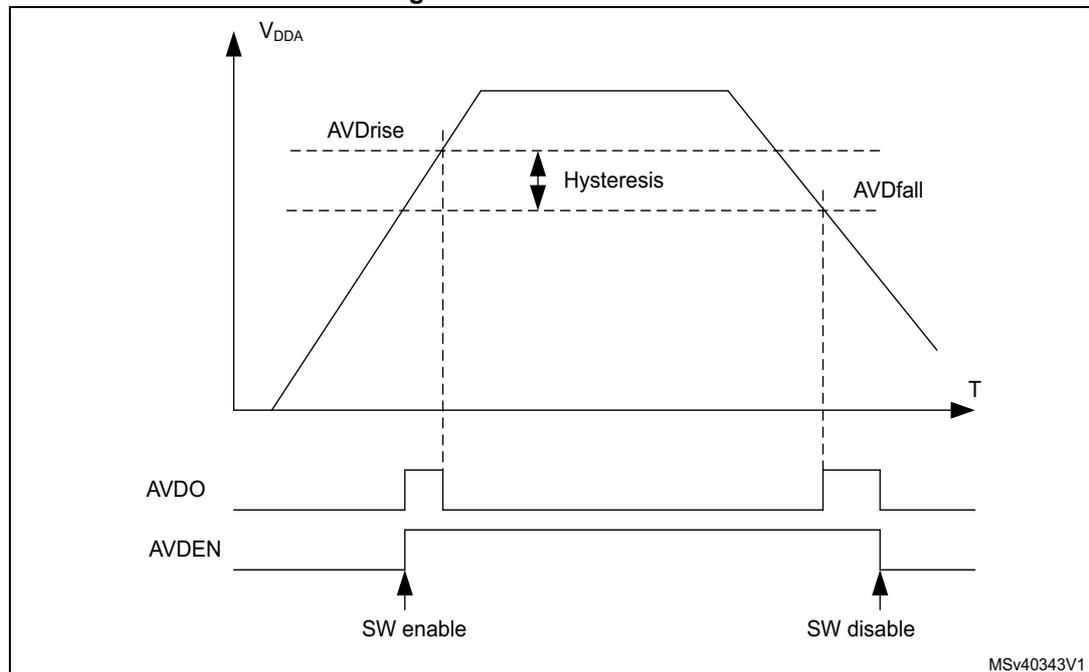
The figure is a timing diagram illustrating the operation of the Analog Voltage Detector (AVD). The top graph shows the \( V_{DDA} \) supply voltage (Y-axis) versus time (X-axis). The voltage rises to a peak and then falls. Two horizontal dashed lines represent the AVD threshold levels: \( AVDrise \) (higher threshold) and \( AVDfall \) (lower threshold). The vertical distance between these two thresholds is labeled 'Hysteresis'. Below the graph, two digital signals are shown: AVDO and AVDEN. The AVDO signal is high when \( V_{DDA} \) is below the \( AVDfall \) threshold and low otherwise. The AVDEN signal is shown being set high by 'SW enable' and low by 'SW disable' at the start and end of the measurement period, respectively. The diagram is labeled MSV40343V1 in the bottom right corner.
- 1. For thresholds and hysteresis values, refer to the datasheets.
6.5.5 Battery voltage thresholds
In \( V_{BAT} \) mode, the battery voltage supply (RTC domain) can be monitored by comparing it with two threshold levels: \( V_{BAThigh} \) and \( V_{BATlow} \) . The \( V_{BAT} \) supply monitoring can be enabled/disabled via MONEN bit in PWR control register 2 (PWR_CR2) . When it is enabled, the battery voltage thresholds increase power consumption.
\( V_{BATH} \) and \( V_{BATL} \) can trigger an internal tamper event (see Section 51: Tamper and backup registers (TAMP) ).
Figure 31. \( V_{BAT} \) thresholds
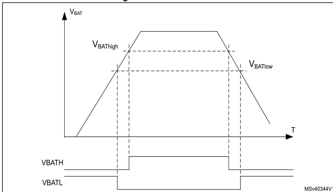
The figure illustrates the relationship between battery voltage ( \( V_{BAT} \) ) and two monitoring thresholds ( \( V_{BATHigh} \) and \( V_{BATlow} \) ) over time ( \( T \) ). The top graph shows \( V_{BAT} \) rising from a low level, crossing \( V_{BATlow} \) and then \( V_{BATHigh} \) , reaching a peak, and then falling back down, crossing \( V_{BATHigh} \) and then \( V_{BATlow} \) . Vertical dashed lines mark these crossing points. Below the graph, two digital signals are shown: \( V_{BATH} \) (Battery Voltage High) and \( V_{BATL} \) (Battery Voltage Low). \( V_{BATH} \) is initially low and goes high when \( V_{BAT} \) crosses \( V_{BATHigh} \) on the rising edge, returning to low when \( V_{BAT} \) crosses \( V_{BATHigh} \) on the falling edge. \( V_{BATL} \) is initially high and goes low when \( V_{BAT} \) crosses \( V_{BATlow} \) on the rising edge, returning to high when \( V_{BAT} \) crosses \( V_{BATlow} \) on the falling edge. The diagram includes hysteresis, indicated by the gap between the rising and falling threshold levels for each signal. The identifier MSV40344V1 is present in the bottom right corner of the diagram area.
- 1. For thresholds and hysteresis values, refer to the datasheets.
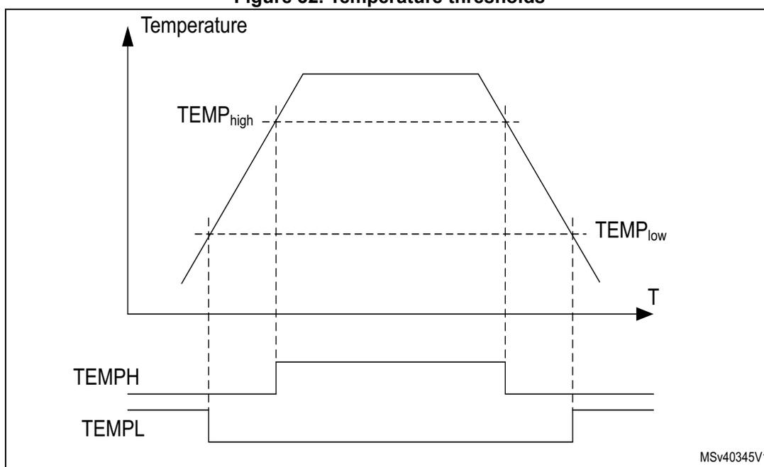
6.5.6 Temperature thresholds
A dedicated temperature sensor cell is embedded in the power control. The junction temperature can be monitored by comparing it with two threshold levels, \( TEMP_{high} \) and \( TEMP_{low} \) . TEMPH and TEMPL flags in the PWR control register 2 (PWR_CR2) , indicate whether the device temperature is higher or lower than the threshold. The temperature monitoring can be enabled/disabled via MONEN bit in PWR control register 2 (PWR_CR2) . When enabled, the temperature thresholds increase power consumption. As an example the levels may be used to trigger a routine to perform temperature control tasks.
TEMPH and TEMPL wake-up interrupts are available on the RTC tamper signals (see Section 51: Tamper and backup registers (TAMP) ).
Figure 32. Temperature thresholds
- 1. For thresholds and hysteresis values, refer to the datasheets.
6.5.7 \( V_{CORE} \) maximum voltage level detector
\( V_{CORE} \) is protected against too high voltages in the direct SMPS step-down converter configuration. \( V_{CORE} \) overvoltage protection is enabled at startup by hardware once the SMPS step-down converter configuration has been programmed into PWR control register 3 (PWR_CR3) . The two following configurations exist:
- •
\(
V_{CORE}
\)
voltage level stays within range:
- – The ACTVOSRDY bit in PWR control status register 1 (PWR_CSR1) indicates valid voltage levels.
- – The system operates normally and \( V_{CORE} \) overvoltage protection is disabled.
- •
\(
V_{CORE}
\)
overvoltages (due to a wrongly programmed SMPS step-down converter):
- – The hardware forces the SMPS step-down converter voltage level to 1.0 V.
- – ACTVOSRDY indicates invalid voltage levels. In this case the software must be corrected and re-loaded to program a correct SMPS step-down converter
configuration that matches the application supply connections. The system must be power cycled.
Figure 33. \( V_{CORE} \) overvoltage protection
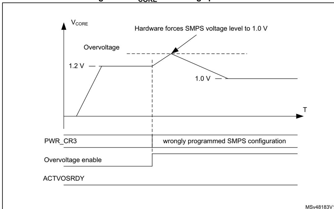
The figure illustrates the \( V_{CORE} \) overvoltage protection mechanism. The top graph plots \( V_{CORE} \) against time (T). The voltage starts at 1.2 V, rises to an overvoltage level, and then drops to 1.0 V. A label 'Hardware forces SMPS voltage level to 1.0 V' points to the 1.0 V level. Below the graph, three timing diagrams show: PWR_CR3 (labeled 'wrongly programmed SMPS configuration'), Overvoltage enable, and ACTVOSRDY. The PWR_CR3 signal is high during the overvoltage event. The Overvoltage enable signal is low. The ACTVOSRDY signal is high.
MSV48183V1
6.6 Power management
The power management block controls the \( V_{CORE} \) supply in accordance with the system operation modes (see Section 6.6.1 ).
The \( V_{CORE} \) domain is split into the following power domains.
- • CPU domain (CD) containing most peripherals and the Cortex ® -M7 Core (CPU)
- • SmartRun domain (SRD) containing some peripherals and the system control
The CPU and SmartRun domains can operate in one of the following operating modes (see Table 35: Operating mode summary ):
- • Run (power ON, clock ON)
- • Autonomous (power ON, SRD domain clock ON)
- • Stop (power ON, clock OFF)
- • Standby (power OFF, clock OFF).
The CPU domain is a power domain that is common to the CPU, DMAs and most of the AXI, AHB and APB peripherals.
The SRD domain includes one DMA, an AHB bus matrix and some APB peripherals. The SDR domain power modes can either follow CPU subsystem modes or remain in Run mode
regardless of CPU subsystem modes. This is done by setting the RUN_SRD bit in the PWR_CPUCR register.
- • If RUN_SRD is set to 1, the SmartRun domain remains in DRun mode, independently from the CPU modes (see Section 6.8.5: PWR CPU control register (PWR_CPUCR) )
- • If RUN_SRD is set to 0, the SmartRun domain enters DStop mode when the CPU enters CStop mode (see Table 35: Operating mode summary ).
The CPU and system SmartRun domains are supplied from a single regulator at a common V CORE level. The V CORE supply level follows the system operating mode (Run, Stop, Standby). The CPU domain can be set in a specific retention level, known as DStop2, whereby the logic is switched off and the register contents are retained. Selection between Dstop or DStop2 is made through the RETDS_CD bit of PWR CPU control register (PWR_CPUCR) .
The content of all memories is retained in DStop and DStop2. Further power saving can be made by selectively switching off individual memory blocks. This is done by means of bits xxxSO bits of PWR control register 1 (PWR_CR1) .
The following voltage scaling features allow controlling the power with respect to the required system performance (see Section 6.6.2: Voltage scaling ):
- • The corresponding voltage scaling must be set in accordance with the system clock frequency. To do this, configure the VOS bits to get the Run mode voltage scaling.
- • In Stop mode, to obtain the best trade-off between static power consumption and exit-from-Stop mode latency, configure the SVOS bits to get Stop mode voltage scaling.
6.6.1 System operating modes
Several system operating modes are available to tune the system according to the performance required, means when the CPU does not need to execute code and is waiting for an external event. It is up to the user to select the operating mode that gives the best compromise between low-power consumption, short startup time and available wake-up sources.
The operating modes allow controlling the clock distribution to the different system blocks and powering them. The system operating mode is driven by the CPU subsystem and system SmartRun autonomous wake-up. The CPU subsystem can span different configurations depending on its peripheral allocation (see Section 8.5.11: Peripheral clock gating control ).
The operating modes described below are available for the different system blocks (see Table 35 ).
Description of the operating mode
System Run modes
Any Run mode voltage scaling can be selected (VOS0, VOS1, VOS2 or VOS3).
- • SRD domain
The system clock and the SmartRun domain bus matrix clock are running.
- • CPU domain
The domain bus matrix is clocked. The CPU subsystem operates in CRun or CSleep mode:
- – CRun
The CPU and CPU subsystem peripheral allocated via PERxEN bits in the RCC registers are clocked.
- – CSleep
The CPU clock is stalled and the CPU subsystem allocated peripheral clock operates according to PERxLPEN bit setting in the RCC registers.
System Autonomous modes
Any Run mode voltage scaling can be selected (VOS0/1/2/3).
- • SRD domain
The system clock and the SmartRun domain bus matrix clocks are running.
- • CPU domain
The CPU and CPU subsystem peripheral clocks are stalled.
The domain bus matrix clock is stalled.
When the CPU subsystem is in CStop mode, the CPU domain is either in DStop or DStop2.
The CPU domain mode selection between DStop and DStop2 is configured via RETDS_CD bit in PWR CPU control register (PWR_CPUCR).
The CPU domain Autonomous modes are the following:
- – Dstop
The CPU domain peripherals able to operate in Stop mode are still operational.
- – Dstop2
The CPU domain peripherals able to operate in Stop mode are no longer operational.
System Stop
Any Stop mode voltage scaling can be selected (SVOS3/4/5).
- • SRD domain
The system clock and the SmartRun domain bus matrix clock are stalled.
- • CPU domain
The CPU and CPU subsystem peripheral clocks are stalled.
The domain bus matrix clock is stalled.
When the CPU subsystem is in CStop mode, the CPU domain is either in DStop or DStop2.
The CPU domain mode selection between DStop and DStop2 is configured via RETDS_CD bit in PWR CPU control register (PWR_CPUCR).
The CPU domain peripherals able to operate in Stop mode are no longer operational. This means that no peripherals in CPU domain are operational.
System Standby
Both SRD and CPU domain supplies are powered down. All internal wake-up signals are inactive.
The Standby mode is selected through the PDDS_SRD bit in PWR CPU control register (PWR_CPUCR).
DStop vs DStop2 mode
DStop2 and DStop modes are very similar from user point of view. In DStop2 mode the asynchronous logic is switched off while RAM and register contents are maintained. This allows further leakage current consumption reduction compared to DStop mode. When exiting DStop2, the CPU domain resumes normal execution at the cost of a slightly higher startup time.
The main differences between DStop and DStop2 are given below:
- • In DStop mode, the entire logic is still supplied.
- • In DStop2 mode, memories and registers are maintained, while asynchronous logic is switched off. This allows further leakage current reduction. Upon exiting DStop2, the CPU domain can resume normal execution.
The system state is retained in DStop and DStop2.
Table 35. Operating mode summary
| System | SRD domain | CPU domain | CPU | Entry | wake-up | System oscillator | System clock | Domain bus matrix clock | Peripheral clock | CPU clock | Voltage regulator | Domain supply | Voltage scaling |
|---|---|---|---|---|---|---|---|---|---|---|---|---|---|
| Run | SRDRun | DRun | CRun | - | - | ON | ON | ON | ON | ON | ON | ON | VOS0/1/2/3 |
| CSleep | WFI or return from ISR or WFE | Any interrupt or event | ON/OFF (1) | ||||||||||
| Autonomous | DStop (2) | CStop | SLEEPDEEP bit + WFI or return from ISR or WFE | Any EXTI interrupt or event | ON | ON | ON | ON/OFF (3) | OFF | ON | RET (9) | SVOS3/4/5 | |
| DStop2 (4) | ON/OFF (3) | ON | |||||||||||
| Stop (5) | SRDStop | DStop (2) | CStop | SLEEPDEEP bit + WFI or return from ISR or WFE or wake-up source cleared (6) | ON/OFF (7) | OFF | OFF | OFF (8) | OFF | OFF | RET (9) | OFF | |
| DStop2 (4) | OFF (8) | ON | |||||||||||
| Standby (10) | PDDS_SRD bit + SLEEPDEEP bit + WFI or return from ISR or WFE or wake-up source cleared (6) | WKUP pins rising or falling edge, RTC alarm (Alarm A or Alarm B), RTC wake-up event, RTC tamper events, RTC timestamp event, external reset in NRST pin, IWDG reset | OFF | OFF | OFF | OFF | OFF | OFF | OFF | OFF | |||
1. The peripherals that have a PERxLPEN bit, operate accordingly.
2. The CPU subsystem is in CStop and RETDS_CD selects DStop.
3. SmartRun domain peripherals having a PERxAMEN bit, operate accordingly.
4. The CPU subsystem is in CStop and RETDS_CD selects DStop2.
5. The CPU domain needs to be in DStop or DStop2 mode, no wake-up signal is active in SmartRun domain and PDDS_SRD bit selects the Stop mode.
6. When the CPU is in CStop and SmartRun domain in Autonomous mode, the last EXTI wake-up source must be cleared to enter System Stop or Standby mode.
- 7. When the system oscillator HSI or CSI is used, the state is controlled by HSIKERON and CSIKERON, otherwise the system oscillator is OFF.
- 8. When the system is in Stop mode, all the peripheral bus interface clocks are OFF. But peripherals in the SmartRun domain having a kernel clock request can stay active by programming their PERxAMEN bit (RCC_SRDMEN).
- 9. Supply level is in retention: content is kept (memories, registers) but domain is not operational.
- 10. PDDS_SRD selects the Standby mode. The whole core domain is switched off.
6.6.2 Voltage scaling
The CPU and SmartRun domains are supplied from a single voltage regulator supporting voltage scaling with the following features:
- • Run mode voltage scaling
- – VOS0: scale 0
- – VOS1: scale 1
- – VOS2: scale 2
- – VOS3: scale 3
- • Stop mode voltage scaling
- – SVOS3: scale 3
- – LP-SVOS4: scale 4
- – LP-SVOS5: scale 5
For more details on voltage scaling values, refer to the product datasheets.
After reset, the system starts on the lowest Run mode voltage scaling (VOS3). The voltage scaling can then be changed on-the-fly by software by programming VOS bits in PWR SmartRun domain control register (PWR_SRDCR) according to the required system performance. When exiting from Stop mode or Standby mode, the Run mode voltage scaling is reset to the default VOS3 value.
Before entering Stop mode, the software can preselect the SVOS level in PWR control register 1 (PWR_CR1) . The Stop mode voltage scaling for SVOS4 and SVOS5 also sets the voltage regulator in Low-power (LP) mode to further reduce power consumption. When preselecting SVOS3, the use of the voltage regulator low-power mode (LP) can be selected by LPDS bit in PWR control register 1 (PWR_CR1) .
Figure 34.\( V_{CORE} \) voltage scaling versus system power modes
The diagram illustrates the voltage scaling options for \( V_{CORE} \) across different system power modes:
- Standby: Includes POWER DOWN . Transitions to Run and Autonomous modes are shown via pink arrows.
- Run: Contains MAIN VOS0 , MAIN VOS1 , MAIN VOS2 , and MAIN VOS3 . A reset signal is associated with MAIN VOS2 . Transitions between these voltage levels are shown via green arrows (SW Run mode).
- Autonomous: Contains MAIN VOS0 , MAIN VOS1 , MAIN VOS2 , and MAIN VOS3 . Transitions between these voltage levels are shown via yellow arrows (Autonomous mode).
- Stop: Contains MAIN or LP SVOS3 , LP SVOS4 , and LP SVOS5 . Transitions from Run and Autonomous to Stop are shown via blue arrows (Stop mode).
- Wakeup: Transitions from Standby , Run , and Stop back to active modes are shown via purple arrows.
Legend:
- SW Run mode (green arrow)
- Autonomous mode (yellow arrow)
- Stop mode (blue arrow)
- Standby mode (pink arrow)
- Wakeup (purple arrow)
MSV48172V2
6.6.3 Power control modes
The power control block handles the \( V_{CORE} \) supply for system Run, Stop and Standby modes.
The system operating mode depends on the CPU subsystem modes (CRun, CSleep, CStop), on the domain modes (DRun, DStop, DStop2) and on the system SmartRun autonomous wake-up:
- • In Run and Autonomous modes,
\(
V_{CORE}
\)
is defined by the VOS voltage scaling.
The CPU subsystem is either in CRun or CSleep, or an EXTI wake-up is active. - • In Stop mode,
\(
V_{CORE}
\)
is defined by the SVOS voltage scaling.
The CPU subsystem is in CStop mode and no EXTI wake-ups are pending. The CPU domain is either in DStop or DStop2 mode. - • In Standby mode,
\(
V_{CORE}
\)
supply is switched off.
The CPU domain and CPU subsystem are powered off and all EXTI wake-ups are inactive, except wake-up pins, Tamper and RTC.
The CPU domain mode selection between DStop and DStop2 is configured via RETDS_CD bit in PWR CPU control register (PWR_CPUCR) . The system/SmartRun mode selection
between Stop and Standby is configured via PDDS_SRD bit in PWR CPU control register (PWR_CPUCR) .
The system enters Standby when PDDS_SRD bit allows it and stays otherwise in Stop mode (CPU domain in DStop or DStop2).
Table 36 describes all possible low-power mode states.
Table 36. PDDS_SRD and RETDS_CD low-power mode control
| PWR_CPUCR | CPU domain mode | SmartRun domain mode | |
|---|---|---|---|
| RETDS_CD | PDDS_SRD | ||
| 0 | 0 | DStop | SDRun or SDStop |
| 1 | DStop2 | ||
| 0 | 1 | Standby | Standby |
| 1 | |||
Figure 35. Power-control modes detailed state diagram
The diagram illustrates the power-control modes and their transitions:
- Run
(Operating mode):
- Sub-modes: CPU CRun or CSleep, CPU domain DRun, SRD domain Run.
- Transitions:
- Entry: reset, Wakeup from Standby.
- Exit to Autonomous: C_Wakeup.
- Exit to Standby: Enter to Standby.
- Exit to Stop: Enter to Stop.
- Autonomous
(Operating mode):
- Sub-modes: CPU CStop, EXTI wakeup active & RUN_SRD = 1, CPU domain DStop/DStop2, SRD domain Run.
- Transitions:
- Entry from Run: C_Wakeup.
- Exit to Run: CStop.
- Exit to Standby: Enter to Standby.
- Exit to Stop: Enter to Stop.
- Self-transition: Autonomous mode.
- Standby
(Operating mode):
- Sub-modes: EXTI wakeups inactive & PDDS_SRD = 1 & RUN_SRD = 0, CPU domain OFF, SRD domain OFF.
- Transitions:
- Entry from Run: Enter to Standby.
- Entry from Autonomous: Enter to Standby.
- Exit to Run: Wakeup from Standby.
- Stop
(Operating mode):
- Sub-modes: CPU CStop, No pending EXTI wakeups & PDDS_SRD = 0 & RUN_SRD = 0, CPU domain Dstop/DStop2, SRD domain Stop.
- Transitions:
- Entry from Run: Enter to Stop.
- Entry from Autonomous: Enter to Stop.
- Exit to Run: Wakeup from Stop.
Legend:
- □ CPU sub-system modes
- ● ● ● Domain modes
- ■ Operating mode
MSV48173V2
After a system reset, the CPU is in CRun mode.
Power control state transitions are initiated by the following events:
- • The CPU goes to CStop mode or wakes up from CStop mode (state transitions in Run mode are marked in green).
- • The system enters or exits Stop mode (state transitions marked in blue)
- – blue transitions: the system enters Stop mode with the CPU domain in DStop or DStop2 and the CPU in CStop. The system wakes up from Stop. The CPU and CPU domain are restarted. When exiting system Stop mode, the STOPF bit is set.
- – yellow transitions: the system toggles between SRDRun and SRDStop, while the CPU domain remains in DStop or DStop2 without waking up (Autonomous mode).
- • The system enters or exits from Standby mode (state transitions are marked in pink).
- – When exiting from Standby mode, the SBF bit is set.
Table 37 shows the flags indicating from which mode the domain/system exits. The CPU features a set of flags that can be read from PWR CPU control register (PWR_CPUCR) .
Table 37. Low-power exit mode flags
| System mode | CPU domain mode | SBF | STOPF | Comment |
|---|---|---|---|---|
| Run | DRun | 0 | 0 | - |
| Autonomous | DStop or DStop2 | 0 | 0 | CPU domain and system contents retained |
| Stop | DStop or DStop2 | 0 | 1 | CPU domain and system contents retained, clock system reset. |
| Standby | OFF | 1 | 0 | CPU domain and system contents lost |
6.6.4 Power management examples
Figure 36 shows \( V_{CORE} \) voltage scaling behavior in Run mode.
Figure 37 shows \( V_{CORE} \) voltage scaling behavior in Stop mode.
Figure 38 shows \( V_{CORE} \) voltage regulator and voltage scaling behavior in Standby mode.
Figure 39 shows \( V_{CORE} \) voltage scaling behavior in Run mode with CPU domain in DStop or DStop2 mode.
Example of \( V_{CORE} \) voltage scaling behavior in Run mode
Figure 36 illustrates the following system operation sequence example:
- 1. After reset, the system starts from HSI with VOS3.
- 2. The system performance is first increased to a medium-speed clock from the PLL with voltage scaling VOS2. To do this:
- a) Program the voltage scaling to VOS2.
- b) Once the \( V_{CORE} \) supply has reached the required level indicated by VOSRDY, increase the clock frequency by enabling the PLL.
- c) Once the PLL is locked, switch the system clock.
- 3. The system performance is then increased to high-speed clock from the PLL with voltage scaling VOS1. To do this:
- a) Program the voltage scaling to VOS1.
- b) Once the \( V_{CORE} \) supply has reached the required level indicated by VOSRDY, increase the clock frequency.
- 4. The system performance is then reduced to a medium-speed clock with voltage scaling VOS2. To do this:
- a) First decrease the system frequency.
- b) Then decrease the voltage scaling to VOS2.
- 5. The next step is to reduce the system performance to HSI clock with voltage scaling VOS3. To do this:
- a) Switch the clock to HSI.
- b) Disable the PLL.
- c) Decrease the voltage scaling to VOS3.
- 6. The system performance can then be increased to high-speed clock from the PLL. To do this:
- a) Program the voltage scaling to VOS1.
- b) Once the \( V_{CORE} \) supply has reached the required level indicated by VOSRDY, increase the clock frequency by enabling the PLL.
- c) Once the PLL is locked, switch the system clock.
When the system performance (clock frequency) is changed, VOS must be set accordingly, otherwise the system might be unreliable.
Figure 36. Dynamic voltage scaling in Run mode
The figure is a timing diagram illustrating dynamic voltage scaling in Run mode. It shows the relationship between voltage scaling levels (VOS 1, 2, 3), the VOSRDY signal, the PLLxON signal, and the system clock (ck_sys, ck_hclk_cd, ck_hclk_srd) during transitions between different performance levels.
The diagram is divided into several horizontal tracks:
- VOS 1, VOS 2, VOS 3: These tracks show the voltage scaling levels. VOS 1 is the highest level, VOS 2 is medium, and VOS 3 is the lowest. The \( V_{CORE} \) supply voltage is shown transitioning between these levels.
- VOSRDY: This signal indicates when the \( V_{CORE} \) supply has reached the required level for the selected VOS level. It is high when the voltage is stable at the current level.
- PLLxON: This signal controls the PLL. It is high when the PLL is enabled and low when it is disabled.
- ck_sys, ck_hclk_cd, ck_hclk_srd: These are clock signals. ck_sys is the system clock, ck_hclk_cd is the core clock, and ck_hclk_srd is the system clock. The frequency of these clocks changes based on the system state (RUN from HSI or Run from PLL).
Below the waveforms, a table shows the status of register bits at each step of the voltage scaling process:
| Status of register bits at each step | RUN | Wait VOSRDY | Wait PLL | RUN | Wait VOSRDY | RUN | Wait VOSRDY | Wait PLL | RUN | |
| RUN from HSI | Run from PLL | RUN from HSI | Run from PLL | |||||||
The diagram shows the following sequence of events:
- The system starts in RUN mode with VOS 3 and ck_sys running from HSI.
- The voltage scaling is changed to VOS 2 . The system enters a Wait VOSRDY state.
- Once VOSRDY is high, the system enters a Wait PLL state as the PLL is enabled.
- Once the PLL is locked, the system enters RUN mode with VOS 1 and ck_sys running from the PLL.
- The voltage scaling is changed to VOS 2 . The system enters a Wait VOSRDY state.
- Once VOSRDY is high, the system enters RUN mode with VOS 2 and ck_sys running from the PLL.
- The voltage scaling is changed to VOS 3 . The system enters a Wait VOSRDY state.
- Once VOSRDY is high, the system enters a Wait PLL state as the PLL is disabled.
- Once the PLL is disabled, the system enters RUN mode with VOS 3 and ck_sys running from HSI.
MSv48174V1
Example of \( V_{CORE} \) voltage scaling behavior in Stop mode
Figure 37 illustrates the following system operation sequence example:
- 1. The system is running from the PLL in high-performance mode (VOS1 voltage scaling).
- 2. The CPU subsystem deallocates all peripherals related to AHB1 and AHB2. As a consequence, the clocks hclk[2:1] and the related APB1 and APB2 peripherals clocks (pclck1 and pclck2) are stopped. The system still provides the high-performance system clock, hence the voltage scaling must stay at VOS1 level.
- 3. In a second step, the CPU subsystem enters CStop mode, the CPU domain enters DStop or DStop2 mode (Dstop or Dstop2 is selected by RETDS_CD bit in PWR CPU control register (PWR_CPUCR) ) and the system enters Stop mode. The system clock is stopped and the hardware lowers the voltage scaling to the software preselected SVOS4 level.
- 4. The CPU subsystem is then woken up. The system exits Stop mode, the CPU domain exits DStop or DStop2 mode and the CPU subsystem exits CStop mode. The hardware then sets the voltage scaling to VOS3 level and waits for the requested supply level to be reached before enabling the HSI clock. Once the HSI clock is stable, the system clock, the CPU domain clock and the CPU subsystem clock are enabled. Several system clock cycles are needed before the bus clocks are activated according to the xxxEN bits in the RCC.
- 5. The CPU subsystem allocates a peripheral in the APB1/APB2 domain. The related hclk and pclck peripheral clocks are enabled.
- 6. The system performance is then increased. To do this:
- a) The software first sets the voltage scaling to VOS1.
- b) Once the \( V_{CORE} \) supply has reached the required level indicated by VOSRDY, the clock frequency can be increased by enabling the PLL.
- c) Once the PLL is locked, the system clock can be switched.
Figure 37. Dynamic voltage scaling behavior with CPU domain and system in Stop mode
The diagram illustrates the dynamic voltage scaling (DVS) behavior when the CPU domain and system enter Stop mode. The signals shown include voltage levels (VOS 1, VOS 2, VCORE, (S)VOS 3, SVOS 4), voltage status (VOSRDY), wake-up signals (exti_c_wkup, pwr_srd_wkup, pwr_cd_wkup), PLL status (PLLxON), and clock signals (ck_sys, ck_fclk, ck_hclk1/2/3, ck_hclk4) for the CPU and SmartRun domains. The bottom part of the diagram is a state transition table:
| CPU Domain RUN SmartRun RUN | STOP | Wait VCORE | Wait HSI | CPU Domain RUN SmartRun RUN | Wait VOSRDY | RUN |
| Run from PLL | Clock Stopped | RUN from HSI | Run from PLL |
MSV48175V1
Example of V CORE voltage regulator/voltage scaling behavior in Standby mode
Figure 38 illustrates the following system operation sequence example:
- 1. The system is running from the PLL in high-performance mode (VOS1 voltage scaling).
- 2. The CPU subsystem deallocates all peripherals related to AHB1 and AHB2. As a consequence the clocks hclk[2:1] and the related APB1 and APB2 peripherals clocks (pclk1 and pclk2) are stopped. The system performance is unchanged hence the voltage scaling does not change.
- 3. The CPU subsystem and the system enters Standby mode (selection through PDDS_SRD bit). The system clock is stopped and the voltage regulator is switched off.
- 4. The system is then woken up by a wake-up source. The system exits Standby mode. The hardware sets the voltage scaling to the default VOS3 level and waits for the requested supply level to be reached before enabling the default HSI oscillator. Once the HSI clock is stable, the system clock and the CPU subsystem clock are enabled. The software must then check the ACTVOSRDY is valid before changing the system performance.
- 5. The CPU subsystem allocates a peripheral in the APB1/APB2 domain. The related hclk and pclk peripheral clocks are enabled.
- 6. In a next step, increase the system performance. To do this:
- a) The software first increases the voltage scaling to VOS1 level.
- b) Before enabling the PLL, the software waits for the requested supply level to be reached by monitoring VOSRDY bit.
- c) Once the PLL is locked, the system clock can be switched.
Figure 38. Dynamic voltage scaling system Standby mode
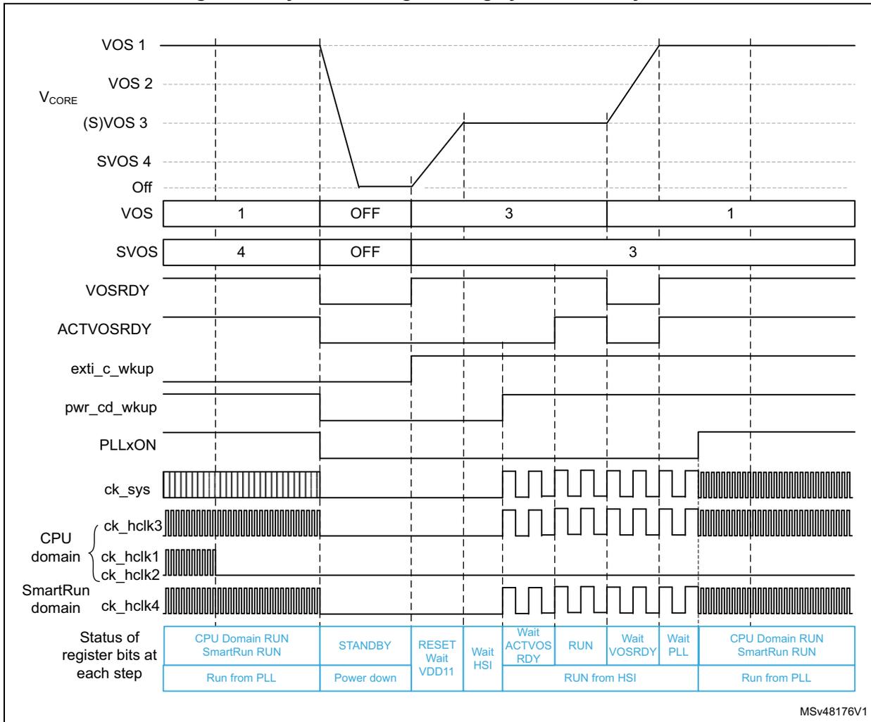
The figure is a timing diagram illustrating the dynamic voltage scaling system in Standby mode. It shows the relationship between various voltage levels, clock signals, and system status over time.
Signal Waveforms:
- VOS 1, VOS 2, VCORE, (S)VOS 3, SVOS 4: These signals represent voltage levels. VOS 1 and VOS 2 are shown as constant high. VCORE and (S)VOS 3 show a step-down to a lower level during the Standby period and a step-up back to the initial level upon waking. SVOS 4 is shown as constant low.
- Off: A signal that goes high during the Standby period.
- VOS, SVOS: Digital representations of the voltage levels. VOS transitions from 1 to OFF and back to 3, then to 1. SVOS transitions from 4 to OFF and back to 3.
- VOSRDY, ACTVOSRDY: Ready signals that go low when voltage levels change and return high when the new levels are stable.
- exti_c_wkup, pwr_cd_wkup: Wake-up signals that go high to exit Standby mode.
- PLLxON: PLL enable signal that goes high after waking up.
- ck_sys, ck_hclk3, ck_hclk1, ck_hclk2, ck_hclk4: Clock signals. ck_sys is the system clock. The CPU domain clocks (ck_hclk3, ck_hclk1, ck_hclk2) and SmartRun domain clock (ck_hclk4) are shown as high-frequency oscillations. They stop during Standby and resume after waking up.
Status of register bits at each step:
| Status of register bits at each step | CPU Domain RUN SmartRun RUN | STANDBY | RESET Wait VDD11 | Wait HSI | Wait ACTVOS RDY | RUN | Wait VOSRDY | Wait PLL | CPU Domain RUN SmartRun RUN |
| Run from PLL | Power down | RUN from HSI | Run from PLL | ||||||
MSV48176V1
Example of V CORE voltage scaling behavior in Run mode with CPU domain in DStop or DStop2 mode
Figure 39 illustrates the following system operation sequence example:
- 1. The system is running from the PLL with system in high-performance mode (VOS1 voltage scaling).
- 2. The CPU subsystem deallocates all peripherals related to AHB1 and AHB2. As a consequence the clocks hclk[2:1] and the related APB1 and APB2 peripherals clocks (pclck1 and pclck2) are stopped. The system performance is unchanged hence the voltage scaling does not change.
- 3. The CPU subsystem then enters CStop mode and the CPU domain enters DStop or DStop2 mode (selected by RETDS_CD bit in PWR CPU control register (PWR_CPUCR) ). The CPU AXI bus matrix clock is stopped. At the same time the system/SmartRun domain enters Stop mode. The system clock is stopped and the hardware lowers the voltage scaling to the software preselected SVOS4 level.
- 4. The system is then woken up by a SmartRun Autonomous mode wake-up event. The system exits Stop mode. The hardware sets the voltage scaling to the default VOS3 level and waits for the requested supply level to be reached before enabling the HSI clock. Once the HSI clock is stable, the system clock is enabled. The system is running in SmartRun Autonomous mode.
- 5. The SmartRun Autonomous mode wake-up source is then cleared, causing the system to enter Stop mode. The system clock is stopped and the voltage scaling is lowered to the software preselected SVOS4 level.
- 6. The CPU subsystem is then woken up. The system exits Stop mode, the CPU domain exits DStop/DStop2 mode and the CPU subsystem exits CStop mode. The hardware sets the voltage scaling to the default VOS3 level and waits for the requested supply level to be reached before enabling the default HSI oscillator. Once the HSI clock is stable, the system clock and the CPU subsystem clock are enabled.
Figure 39. Dynamic voltage scaling behavior with CPU domain in DStop or DStop2 mode and SmartRun domain in Autonomous mode
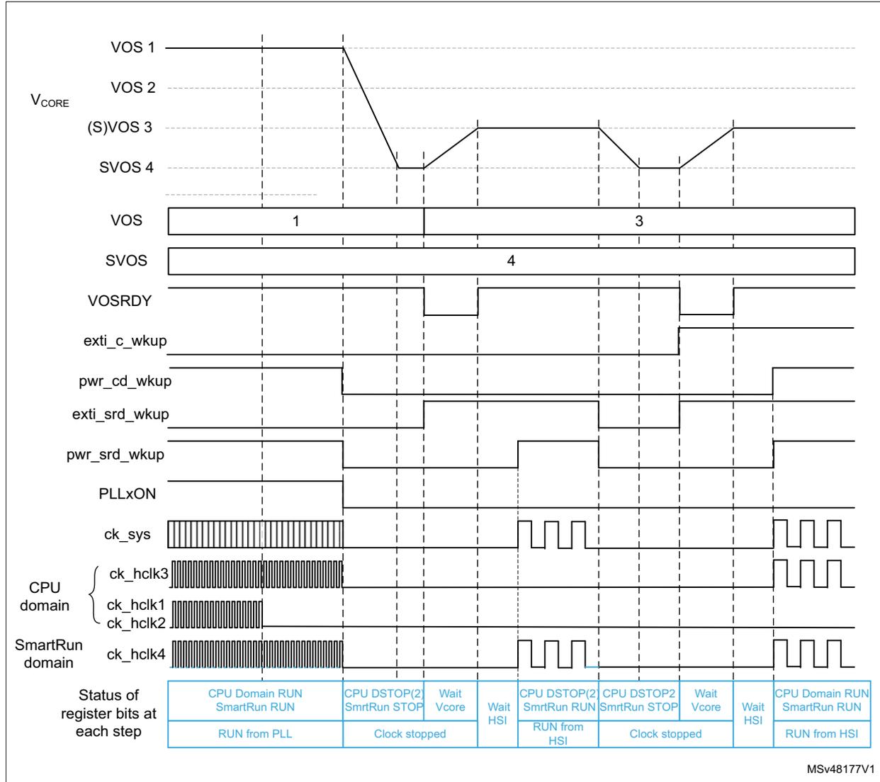
The figure is a timing diagram illustrating the dynamic voltage scaling (DVS) behavior. The signals shown are:
- V CORE : Core voltage levels VOS 1, VOS 2, (S)VOS 3, and SVOS 4. The diagram shows transitions between these levels.
- VOS : Voltage scaling mode register bits. It is divided into two segments: '1' and '3'.
- SVOS : System voltage scaling mode register bit, set to '4'.
- VOSRDY : Voltage scaling ready flag.
- exti_c_wkup : External interrupt wake-up signal for the CPU domain.
- pwr_cd_wkup : Power control wake-up signal for the CPU domain.
- exti_srd_wkup : External interrupt wake-up signal for the SmartRun domain.
- pwr_srd_wkup : Power control wake-up signal for the SmartRun domain.
- PLLxON : PLL on/off control signal.
- ck_sys : System clock signal.
- CPU domain : Contains clock signals ck_hclk3, ck_hclk1, and ck_hclk2.
- SmartRun domain : Contains clock signal ck_hclk4.
At the bottom, a table shows the status of register bits at each step of the sequence:
| Status of register bits at each step | CPU Domain RUN SmartRun RUN | CPU DSTOP(2) SmrRun STOP | Wait Vcore | Wait HSI | CPU DSTOP(2) SmrRun RUN | CPU DSTOP2 SmrRun STOP | Wait Vcore | Wait HSI | CPU Domain RUN SmartRun RUN |
| RUN from PLL | Clock stopped | RUN from HSI | Clock stopped | RUN from HSI | |||||
MSV48177V1
6.7 Low-power modes
Several low-power modes are available to save power when the CPU does not need to execute code (when waiting for an external event). It is up to the user application to select the mode that gives the best compromise between low-power consumption, short startup time and available wake-up sources:
- • Slowdown of system clocks: see Section 8.5.6: System clock (sys_ck)
- • Control of individual peripheral clocks, see Section 8.5.11: Peripheral clock gating control
- • Available low-power modes (see
Table 35: Operating mode summary
and
Figure 35: Power-control modes detailed state diagram
):
- – System Run, SRDRun, DRun and CSleep modes
Only the Arm ® Cortex ® -M7 (CPU subsystem) clock is stopped (CSleep). - – System Autonomous, SRDRun, DStop/DStop2 and CStop modes
The SRD domain is running (SRDRun).
All the clocks in the CPU domain are stopped (CStop).
The CPU domain is in DStop or Retention mode (DStop2). - – System Stop, SRDStop, DStop /DStop2 and CStop modes
All clocks stopped for all domains
Some clocks can remain active on demand (see Section 6.7.7: Stop mode ).
The CPU domain is in DStop or DStop2 (Retention mode). - – System Standby
The system is powered down.
- – System Run, SRDRun, DRun and CSleep modes
6.7.1 Slowing down system clocks
In Run mode the speed of the system clock
ck_sys
can be reduced. For more details refer to
Section 8.5.6: System clock (sys_ck)
.
6.7.2 Controlling peripheral clocks
In Run mode, the HCLKx and PCLKx for individual peripherals can be stopped by configuring at any time PERxEN bits in
RCC_C1_xxxxENR
or
RCC_DnxxxxENR
to reduce power consumption.
To reduce power consumption in CSleep mode, the individual peripheral clocks can be disabled by configuring PERxLPEN bits in
RCC_C1_xxxxLPENR
or
RCC_DnxxxxLPENR
. For the peripherals still receiving a clock in CSleep mode, their clock can be slowed down before entering CSleep mode and clock gating can be enabled (
RCC_CKGAENR
register).
In Autonomous mode, the individual peripheral clocks can remain active by setting the corresponding PERxAMEN bit of
RCC_SRDAMR
register.
6.7.3 Entering low-power modes
The MCU enters one of the power mode listed in Section 6.7: Low-power modes when executing the WFI (wait for interrupt) or WFE (wait for event) instructions, or when the SLEEPONEXIT bit in the Cortex ® -M system control register is set on Return from ISR.
The system can enter Stop or Standby low-power mode when all EXTI wake-up sources are cleared (see Figure 35 ).
6.7.4 Exiting from low-power modes
The CPU subsystem exits CSleep mode through any interrupt or event depending on how the low-power mode was entered:
- • If the WFI instruction or Return from ISR was used to enter to low-power mode, any peripheral interrupt acknowledged by the NVIC can wake up the system.
- • If the WFE instruction is used to enter to low-power mode, the CPU exits low-power mode as soon as an event occurs. The wake-up event can be generated by one of the followings:
- – an NVIC IRQ interrupt
When SEVONPEND = 0 in the Cortex ® -M7 system control register, the interrupt must be enabled in the peripheral control register and in the NVIC.
When the MCU resumes from WFE, the peripheral interrupt pending bit and the NVIC peripheral IRQ channel pending bit (in the NVIC interrupt clear pending register) have to be cleared. Only NVIC interrupts with sufficient priority wake up and interrupt the MCU.
When SEVONPEND = 1 in the Cortex ® -M7 system control register, the interrupt must be enabled in the peripheral control register and optionally in the NVIC. When the MCU resumes from WFE, the peripheral interrupt pending bit and, when enabled, the NVIC peripheral IRQ channel pending bit (in the NVIC interrupt clear pending register) have to be cleared.
All NVIC interrupts wake up the MCU, even the disabled ones.
Only enabled NVIC interrupts with sufficient priority wake up and interrupt the MCU.
- – an event
An EXTI line must be configured in event mode. When the CPU resumes from WFE, it is not necessary to clear the EXTI peripheral interrupt pending bit or the NVIC IRQ channel pending bit, as the pending bits corresponding to the event line are not set. It might be necessary to clear the interrupt flag in the peripheral.
The MCU exits the Autonomous mode (SRDRun, DStop/DStop2, CStop) or Stop mode (SRDStop, DStop/DStop2, CStop) by enabling an EXTI interrupt or event depending on how the low-power mode was entered (see above).
In Autonomous mode the system can wake up from Stop mode by enabling an EXTI wake-up, without waking up the CPU subsystem.
The MCU exits from Standby mode by enabling an external reset (NRST pin), an IWDG reset, a rising edge on one of the enabled WKUPx pins or a RTC event. Program execution restarts in the same way as after a system reset (such as boot pin sampling, option bytes loading or reset vector fetched).
6.7.5 System Run and CSleep modes
The system remains in Run mode with both the SRD and CPU domains are in Run mode (see Table 35: Operating mode summary ).
The CSleep mode applies only to the CPU subsystem. In this mode, the CPU clock is stopped and the CPU subsystem peripheral clocks operate according to the configuration defined in PERxLPEN bits of RCC_xxxxLPENR registers.
Entering CSleep mode
The CSleep mode is entered according to Section 6.7.3: Entering low-power modes when the SLEEPDEEP bit in the Cortex ® -M System Control register is cleared.
Refer to Table 38 for details on how to enter CSleep mode.
Exiting from CSleep mode
The CSleep mode is exited according to Section 6.7.4: Exiting from low-power modes .
Refer to Table 38 for more details on how to exit from CSleep mode.
Table 38. CSleep mode
| CSleep mode | Description |
|---|---|
| Mode entry | WFI (Wait for Interrupt) or WFE (Wait for Event) while:
|
| Mode exit | If WFI or return from ISR was used for entry:
|
| wake-up latency | None |
6.7.6 System Autonomous mode
In Autonomous mode the SRD domain remains in Run mode while the CPU domain is in DStop or DStop2.
The whole CPU domain is in low-power mode and all the clocks of this domain are stopped. The CPU subsystem included in the CPU domain is in the same mode.
The CPU clock is stopped as well as the peripheral clocks of the CPU domain.
Only the SmartRun domain peripherals associated to a PERxAMEN bit operate according to this bit configuration and can request a kernel clock, if relevant.
The flash memory can be in low-power mode when it is enabled through the FLPS bit of the PWR_CR1 register. This allows a trade-off between CPU domain DStop/DStop2 restart time and low-power consumption.
Entering Autonomous mode
The Autonomous mode is entered according to Section 6.7.3: Entering low-power modes , when the SLEEPDEEP bit in the Cortex®-M System Control register is set.
The CPU domain enters DStop or DStop2 depending on the configuration of RETDS_CD bit of PWR_CPUCR register.
Before entering DStop2 mode, it is mandatory to configure the flash memory in low-power mode by setting the FLPS bit of PWR_CR1.
Before entering DStop2, all the peripherals belonging to the CPU domain and having a kernel clock must be either disabled by clearing the enable bit in the peripheral itself, or reset by setting the corresponding bit in the associated AHB peripheral reset register (RCC_AHBxRSTR) or APB peripheral reset register (RCC_APBxRSTR).
Warning: The user must ensure that no allocated peripheral in the CPU domain has an active kernel clock, or are still clocked by LSI LSE, HSI or CSI. The flash memory must be configured in low-power mode (FLPS bit set in PWR_CR1 register) before entering DStop2.
Refer to Table 39 for details on how to enter Autonomous mode.
Exiting Autonomous mode
The Autonomous mode is exited according to Section 6.7.4: Exiting from low-power modes .
Refer to Table 39 for more details on how to exit from Autonomous mode.
Table 39. Autonomous mode
| Autonomous mode | Description |
|---|---|
| Mode entry | WFI (Wait for Interrupt) or WFE (Wait for Event) while:
On return from ISR while:
|
Table 39. Autonomous mode
| Autonomous mode | Description |
|---|---|
| Mode exit | If WFI or return from ISR was used for entry:
If WFE was used for entry and SEVONPEND = 0:
If WFE was used for entry and SEVONPEND = 1:
|
| Wake-up latency | EXTI and RCC wake-up synchronization (see Section 8.4.7: Power-on and wake-up sequences ) |
I/O states in Autonomous mode
The I/O pin configuration remains unchanged in Autonomous mode.
6.7.7 Stop mode
In system Stop mode, the SRD domain is in Stop mode with the CPU domain in DStop or DStop2. The system clock including a PLL and the SmartRun domain bus matrix clocks are stopped.
The HSI or CSI can remain enabled in system Stop mode (HSIKERON and CSIKERON set in RCC_CR register). After exiting Stop mode, the clock is quickly available as kernel clock for peripherals. Other system oscillator sources are stopped and require a starting time after exiting Stop mode.
In system Stop mode, the following features can be selected to remain active by programming individual control bits:
- • Independent watchdog (IWDG)
The IWDG is started by writing to its key register or by hardware option. Once started it cannot be stopped except by a reset (see Section 49: Independent watchdog (IWDG) ). - • Real-time clock (RTC)
This is configured via the RTCEN bit in the RCC Backup Domain Control Register (RCC_BDCR). - • Internal RC oscillator (LSI RC)
This is configured via the LSION bit in the RCC Clock Control and Status Register (RCC_CSR). - • External 32.768 kHz oscillator (LSE OSC)
This is configured via the LSEON bit in the RCC Backup Domain Control Register (RCC_BDCR).
- • Peripherals in SmartRun domain capable of running on the LSI or LSE clock
- • Peripherals in SmartRun domain having a kernel clock request
In this case the PERxAMEN bit of these peripherals must be set to request the kernel clock (in the RCC_SRDAMR register)
- • Peripherals in CPU domain capable of running on the LSI or LSE clock, if CPU domain is in DStop mode (as opposed to DStop2)
- • Peripherals in the CPU domain having a kernel clock request, if the CPU domain is in DStop mode (as opposed to DStop2)
- • Internal RC oscillators (HSI and CSI)
This is configured via the HSIKERON and CSIKERON bits in the RCC Clock Control and Status Register (RCC_CSR).
- • The ADC or DAC can also consume power during Stop mode, unless they are disabled before entering this mode. To disable them, the ADON bit in the ADC_CR2 register and the ENx bit in the DAC_CR register must both be written to 0.
The selected SVOS4 and SVOS5 levels add an additional startup delay when exiting from system Stop mode (see Table 40 ). An extra latency is added upon entering and exiting DStop2 mode as well.
Table 40. Stop mode operation
| SVOS | LPDS | Stop mode voltage regulator operation | Wake-up latency |
|---|---|---|---|
| SVOS3 | 0 | Main | No additional wake-up time |
| 1 | LP | Voltage regulator wake-up time from Low-power mode | |
| SVOS4 or SVOS5 | x | LP | Voltage regulator wake-up time from Low-power mode + voltage level wake-up time for SVOS4 or SVOS5 level to VOS3 level |
The flash memory can be in Stop mode when it is enabled through the FLPS bit of the PWR_CR1 register. This allows a trade-off between CPU domain DStop/DStop2 restart time and low-power consumption.
RAM memory shut-off
In DStop or DStop2 mode, the content of the memory blocks is maintained. Further power optimization can be obtained by switching off some memory blocks. This optimization implies loss of the memory content. The user can select which memory is discarded during Stop mode by means of xxSO bits in PWR control register 1 (PWR_CR1) as indicated in Table 42 .
Table 41. Memory shut-off block selection
| Selection bit | Shut-off block during Stop mode (DStop or DStop2) |
|---|---|
| AXIRAM1SO | AXI SRAM1 shut-off control |
| AXIRAM2SO | AXI SRAM2 shut-off control |
| Selection bit | Shut-off block during Stop mode (DStop or DStop2) |
|---|---|
| AXIRAM3SO | AXI SRAM3 shut-off control |
| AHBRAM1SO | AHB SRAM1 shut-off control |
| AHBRAM2SO | AHB SRAM2 shut-off control |
| ITCMSO | ITCM and ETM memories shut-off control |
| GFXSO | GFXMMU and JPEG memory shut-off control |
| HSITFSO | High-speed interface USB and FDCAN memories shut-off control |
| SRDRAMSO | SmartRun AHB SRAM shut-off control |
Entering Stop mode
The Stop mode is entered according to Section 6.7.3: Entering low-power modes .
Refer to Table 42 for details on how to enter Stop mode.
If the flash memory programming is ongoing, the Stop mode entry is delayed until the memory access is finished.
If an access to a bus matrix is ongoing, the Stop mode entry is delayed until the bus matrix access is finished.
Warning:
The user must ensure that no peripherals allocated in the CPU domain have an active kernel clock or are still clocked by LSI, LSE, HSI or CSI.
The flash memory must be configured in low-power mode (FLPS bit set in PWR_CR1 register) before entering DStop2.
Exiting from Stop mode
The Stop mode is exited according to Section 6.7.4: Exiting from low-power modes .
Refer to Table 42 for more details on how to exit from Stop mode.
When exiting Stop mode, the system clock, the SmartRun domain bus matrix clocks and voltage scaling are reset.
STOPF status flag in PWR CPU control register (PWR_CPUCR) indicates that the system has exited Stop mode (see Table 37 ).
Table 42. Stop mode| Stop mode | Description |
|---|---|
| Mode entry | When the CPU is in CStop mode and there is no active EXTI wake-up source and RUN_SRD = 0 (in PWR_CPUCR register) |
| Mode exit | On a EXTI wake-up |
| Wake-up latency | System oscillator startup (when disabled) + EXTI and RCC wake-up synchronization + Voltage scaling refer to Table 40 (see Section 6.6.2: Voltage scaling ) + Exiting DStop2 |
I/O states in Stop mode
The I/O pin configuration remains unchanged in Stop mode.
6.7.8 Standby mode
The Standby mode allows achieving the lowest power consumption. Like Stop mode, it is based on CPU subsystem CStop mode. However the V CORE supply regulator is powered off.
The system SmartRun domain enters Standby mode only when the CPU domain is in DStop or DStop2, no EXTI is pending and PDDS_SRD bit selects Standby. When the system/SmartRun domain enters Standby mode, the voltage regulator is disabled. The complete V CORE domain is consequently powered off. The PLLs, HSI oscillator, CSI oscillator, HSI48 and HSE oscillator are also switched off. The content of SRAM and registers is lost except for Backup domain registers (RTC registers, RTC backup register and backup RAM), and Standby circuitry (see Section 6.4.5: Backup domain ).
In system Standby mode, the following features can be selected by programming individual control bits:
- • Independent watchdog (IWDG)
The IWDG is started by programming its key register or by hardware option. Once started, it cannot be stopped except by a reset (see Section 49: Independent watchdog (IWDG) ). - • Real-time clock (RTC)
This is configured via the RTCEN bit in the Backup domain control register (RCC_BDCR). - • Internal RC oscillator (LSI RC)
This is configured by the LSION bit in the control/status register (RCC_CSR). - • External 32.768 kHz oscillator (LSE OSC)
This is configured by the LSEON bit in the Backup domain control register (RCC_BDCR).
Entering Standby mode
The Standby mode is entered according to Section 6.7.3: Entering low-power modes , when the PDDS_SRD bit requests Standby (in PWR CPU control register (PWR_CPUCR) ).
Refer to Table 44 for more details on how to enter Standby mode.
Exiting from Standby mode
The Standby mode is exited according to Section 6.7.4: Exiting from low-power modes .
Refer to Table 44 for more details on how to exit from Standby mode.
The system exits from Standby mode when an external reset (NRST pin), an IWDG reset, a WKUP pin event, a RTC alarm, a tamper event, or a timestamp event is detected. All registers are reset after waking up from Standby except for power control and status registers (PWR control register 2 (PWR_CR2), PWR control register 3 (PWR_CR3)), SBF bit in PWR CPU control register (PWR_CPUCR), PWR wake-up flag register (PWR_WKUPFR), and PWR wake-up enable and polarity register (PWR_WKUPEPR).
After waking up from Standby mode, the program execution restarts in the same way as after a system reset (boot option sampling, boot vector reset fetched). The SBF status flag in PWR CPU control register (PWR_CPUCR) indicates from which mode the system has exited (see Table 43 ).
Table 43. Standby and Stop flags
| SBF | STOPF | Description |
|---|---|---|
| 0 | 1 | System has been in or exits from Stop. |
| 1 | 0 | System exits from Standby. |
Table 44. Standby mode
| Standby mode | Description |
|---|---|
| Mode entry |
|
| Mode exit | WKUP pins rising or falling edge, RTC alarm (Alarm A and Alarm B), RTC wake-up, tamper event, timestamp event, external reset in NRST pin, IWDG reset |
| Wake-up latency | System reset phase (see Section 8.4.2: System reset ) |
I/O states in Standby mode
In Standby mode, all I/O pins are high impedance without pull, except for:
- • Reset pad (still available)
- • PC14 and PC15 pins if configured for LSE oscillator
- • PC13 pin if configured as RTC_OUT1, RTC_TS, TAMP_IN1, TAMP_OUT2 or TAMP_OUT3, assuming they have been configured by the RTC or the TAMPER
- • PI8 pin if configured as RTC_OUT2, TAMP_IN2 or TAMP_OUT3, assuming they have been configured by the RTC or the TAMPER
- • PC1 pin if configured as TAMP_IN3, assuming it has been configured by the TAMPER
- • WKUP pins (if enabled).
The WKUP pin pull configuration can be defined through WKUPPUPDx[1:0] bits in PWR wake-up enable and polarity register (PWR_WKUPEPR) .
6.7.9 Monitoring low-power modes
The devices feature state monitoring pins that monitor the CPU and Domain state transitions to low-power mode (refer to Table 45 for the list of pins and their description). The GPIO pin corresponding to each monitoring signal has to be programmed in alternate function mode.
This feature is not available in Standby mode since these I/O pins are switched to high impedance.
Table 45. Overview of low-power mode monitoring pins
| Power state monitoring pins | Description | Pin assignment |
|---|---|---|
| CSLEEP | CPU clock OFF | PC3 |
| CSTOP | CPU domain in low-power mode | PC2 |
| NDSTOP2 | CPU domain Retention mode selection | PA5 |
The state of the monitoring pins reflect the mode of the CPUs and domains. Refer to Table 46 for a description of the GPIO state depending on the CPU and domain state.
Table 46. GPIO state according to CPU and domain state
| CSLEEP | CSTOP | NDSTOP2 | CPU domain power state | SRD domain power state | CPU state |
|---|---|---|---|---|---|
| 0 | 0 | 1 | DRUN | SRDRUN | CRun |
| 1 | 0 | 1 | DRUN | SRDRUN | CSleep |
| 1 | 1 | 1 | DStop | SRDRUN or SRDStop | CStop |
| 1 | 1 | 0 | DStop2 | SRDRUN or SRDStop | CStop |
6.8 PWR registers
The PWR registers can be accessed in word, half-word and byte format, unless otherwise specified.
6.8.1 PWR control register 1 (PWR_CR1)
Address offset: 0x000
Reset value: 0xF000 C000
| 31 | 30 | 29 | 28 | 27 | 26 | 25 | 24 | 23 | 22 | 21 | 20 | 19 | 18 | 17 | 16 |
|---|---|---|---|---|---|---|---|---|---|---|---|---|---|---|---|
| Res. | Res. | Res. | Res. | SRDRAMSO | HSITFSO | GFXSO | ITCMSO | AHBRAM2SO | AHBRAM1SO | AXIRAM3SO | AXIRAM2SO | AXIRAM1SO | ALS[1:0] | AVDEN | |
| r/w | r/w | r/w | r/w | r/w | r/w | r/w | r/w | r/w | r/w | r/w | r/w | ||||
| 15 | 14 | 13 | 12 | 11 | 10 | 9 | 8 | 7 | 6 | 5 | 4 | 3 | 2 | 1 | 0 |
|---|---|---|---|---|---|---|---|---|---|---|---|---|---|---|---|
| SVOS[1:0] | AVD_READY | BOOSTE | Res. | Res. | FLPS | DBP | PLS[2:0] | PVDE | Res. | Res. | LPDS | ||||
| r/w | r/w | r/w | r/w | r/w | r/w | r/w | r/w | r/w | r/w | r/w | |||||
Bits 31:28 Reserved, must be kept at reset value.
Bit 27 SRDRAMSO : SmartRun domain AHB memory shut-off in DStop/DStop2 low-power mode
0: SmartRun domain AHB memory content is kept in DStop or DStop2 mode
1: SmartRun domain AHB memory content is lost in DStop or DStop2 mode
Bit 26 HSITFSO : high-speed interfaces USB and FDCAN memory shut-off in DStop/DStop2 mode
0: USB and FDCAN memories content is kept in DStop or DStop2 mode
1: USB and FDCAN memories content is lost in DStop or DStop2 mode
Bit 25 GFXSO : GFXMMU and JPEG memory shut-off in DStop/DStop2 mode
0: GFXMMU and JPEG memory content is kept in DStop or DStop2 mode
1: GFXMMU and JPEG memory content is lost in DStop or DStop2 mode
Bit 24 ITCMSO : instruction TCM and ETM memory shut-off in DStop/DStop2 mode
0: ITCM and ETM memories content is kept in DStop or DStop2 mode
1: ITCM and ETM memories content is lost in DStop or DStop2 mode
Bit 23 AHBRAM2SO : AHB SRAM2 shut-off in DStop/DStop2 mode
0: AHB SRAM2 content is kept in DStop or DStop2 mode
1: AHB SRAM2 content is lost in DStop or DStop2 mode
Bit 22 AHBRAM1SO : AHB SRAM1 shut-off in DStop/DStop2 mode
0: AHB SRAM1 content is kept in DStop or DStop2 mode
1: AHB SRAM1 content is lost in DStop or DStop2 mode
Bit 21 AXIRAM3SO : AXI SRAM3 shut-off in DStop/DStop2 mode
0: AXI SRAM3 content is kept in DStop or DStop2 mode
1: AXI SRAM3 content is lost in DStop or DStop2 mode
Bit 20 AXIRAM2SO : AXI SRAM2 shut-off in DStop/DStop2 mode
0: AXI SRAM2 content is kept in DStop or DStop2 mode
1: AXI SRAM2 content is lost in DStop or DStop2 mode
Bit 19 AXIRAM1SO : AXI SRAM1 shut-off in DStop/DStop2 mode
0: AXI SRAM1 content is kept in DStop or DStop2 mode
1: AXI SRAM1 content is lost in DStop or DStop2 mode
Bits 18:17 ALS[1:0] : analog voltage detector level selection
These bits select the voltage threshold detected by the AVD.
00: 1.7 V
01: 2.1 V
10: 2.5 V
11: 2.8 V
Bit 16 AVDEN : peripheral voltage monitor on \( V_{DDA} \) enable
0: peripheral voltage monitor on \( V_{DDA} \) disabled
1: peripheral voltage monitor on \( V_{DDA} \) enabled
Bits 15:14 SVOS[1:0] : system stop mode voltage scaling selection
These bits control the \( V_{CORE} \) voltage level in system Stop mode, to obtain the best trade-off between power consumption and performance.
00: reserved
01: SVOS5 scale 5
10: SVOS4 scale 4
11: SVOS3 scale 3 (default)
Bit 13 AVD_READY : analog voltage ready
This bit is only used when the analog switch boost needs to be enabled (see BOOSTE bit).
It must be set by software when the expected \( V_{DDA} \) analog supply level is available.
The correct analog supply level is indicated by the AVDO bit (PWR_CSR1 register) after setting the AVDEN bit and selecting the supply level to be monitored (ALS bits).
0: peripheral analog voltage \( V_{DDA} \) not ready (default)
1: peripheral analog voltage \( V_{DDA} \) ready
Bit 12 BOOSTE : analog switch VBoost control
This bit enables the booster to guarantee the analog switch AC performance when the \( V_{DD} \) supply voltage is below 2.7 V (reduction of the total harmonic distortion to have the same switch performance over the full supply voltage range)
The \( V_{DD} \) supply voltage can be monitored through the PVD and the PLS bits.
0: booster disabled (default)
1: booster enabled if analog voltage ready (AVD_READY = 1)
Bits 11:10 Reserved, must be kept at reset value.
Bit 9 FLPS : Flash memory low-power mode in DStop or DStop2 mode
When it is set, the flash memory enters Low-power mode when the CPU domain is in DStop/DStop2 mode.
The power consumption is improved with a slightly longer wake-up time.
It is mandatory to set FLPS before entering DStop2 mode.
0: Flash memory remains in normal mode when the CPU domain enters DStop (quick restart time).
1: Flash memory enters Low-power mode when the CPU domain enters DStop/DStop2 (low-power consumption).
Bit 8 DBP : disable Backup domain write protection
In reset state, the RCC_BDCR register, the RTC registers (including the backup registers), BREN and MOEN bits in PWR_CR2 register, are protected against parasitic write access. This bit must be set to enable write access to these registers.
0: access to RTC, RTC backup registers and backup SRAM disabled
1: access to RTC, RTC backup registers and backup SRAM enabled
Bits 7:5 PLS[2:0] : programmable voltage detector level selection
These bits select the voltage threshold detected by the PVD.
000: 1.95 V
001: 2.1 V
010: 2.25 V
011: 2.4 V
100: 2.55 V
101: 2.7 V
110: 2.85 V
111: PVD_IN pin
Note: Refer to Section “Electrical characteristics” of the product datasheet for more details.
Bit 4 PVDE : programmable voltage detector enable
0: programmable voltage detector disabled
1: programmable voltage detector enabled
Bits 3:1 Reserved, must be kept at reset value.
Bit 0 LPDS : low-power DeepSleep with SVOS3 (SVOS4 and SVOS5 always use low-power, regardless of the setting of this bit)
0: LDO voltage regulator or SMPS step-down converter in Main mode (MR) when SVOS3 selects Stop
1: LDO voltage regulator or SMPS step-down converter in Low-power mode (LPR) when SVOS3 selects Stop
6.8.2 PWR control status register 1 (PWR_CSR1)
Address offset: 0x004
Reset value: 0x0000 4000
| 31 | 30 | 29 | 28 | 27 | 26 | 25 | 24 | 23 | 22 | 21 | 20 | 19 | 18 | 17 | 16 |
|---|---|---|---|---|---|---|---|---|---|---|---|---|---|---|---|
| Res. | Res. | Res. | Res. | Res. | Res. | Res. | Res. | Res. | Res. | Res. | Res. | Res. | Res. | MMC/DO | AVDO |
| r | r | ||||||||||||||
| 15 | 14 | 13 | 12 | 11 | 10 | 9 | 8 | 7 | 6 | 5 | 4 | 3 | 2 | 1 | 0 |
| ACTVOS[1:0] | ACTVOSRDY | Res. | Res. | Res. | Res. | Res. | Res. | Res. | Res. | PVDO | Res. | Res. | Res. | Res. | |
| r | r | r | r |
Bits 31:18 Reserved, must be kept at reset value.
Bit 17 MMCVDO : voltage detector output on \( V_{DDMMC} \)
This bit is set and cleared by hardware.
0: \( V_{DDMMC} \) is below 1.2 V.
1: \( V_{DDMMC} \) is above or equal to 1.2 V.
Bit 16 AVDO : analog voltage detector output on \( V_{DDA} \)
This bit is set and cleared by hardware. It is valid only if AVD on \( V_{DDA} \) is enabled by the AVDEN bit.
0: \( V_{DDA} \) is equal or higher than the AVD threshold selected with the ALS[2:0] bits.
1: \( V_{DDA} \) is lower than the AVD threshold selected with the ALS[2:0] bits.
Note: Since the AVD is disabled in Standby mode, this bit is equal to 0 after Standby or reset until the AVDEN bit is set.
Bits 15:14 ACTVOS[1:0] : VOS currently applied for \( V_{CORE} \) voltage scaling selection.
These bits reflect the last VOS value applied to the voltage regulator.
Bit 13 ACTVOSRDY : Voltage levels ready bit for currently used VOS
This bit is set to 1 by hardware when the voltage regulator and the SMPS step-down converter are both disabled and Bypass mode is selected in PWR control register 3 (PWR_CR3).
0: voltage level invalid, above or below current VOS selected level
1: voltage level valid, at current VOS selected level
Bits 12:5 Reserved, must be kept at reset value.
Bit 4 PVDO : programmable voltage detect output
This bit is set and cleared by hardware. It is valid only if the PVD has been enabled by the PVDE bit.
0: \( V_{DD} \) is equal or higher than the PVD threshold selected through the PLS[2:0] bits.
1: \( V_{DD} \) is lower than the PVD threshold selected through the PLS[2:0] bits.
Note: since the PVD is disabled in Standby mode, this bit is equal to 0 after Standby or reset until the PVDE bit is set.
Bits 3:0 Reserved, must be kept at reset value.
6.8.3 PWR control register 2 (PWR_CR2)
Address offset: 0x008
Reset value: 0x0000 0000
This register is not reset by wake-up from Standby mode, RESET signal and \( V_{DD} \) POR. It is only reset by \( V_{SW} \) POR and VSWRST reset.
This register must not be accessed when VSWRST bit in RCC_BDCR register resets the \( V_{SW} \) domain.
After reset, PWR_CR2 register is write-protected. Prior to modifying its content, the DBP bit in PWR_CR1 register must be set to disable the write protection.
| 31 | 30 | 29 | 28 | 27 | 26 | 25 | 24 | 23 | 22 | 21 | 20 | 19 | 18 | 17 | 16 |
|---|---|---|---|---|---|---|---|---|---|---|---|---|---|---|---|
| Res. | Res. | Res. | Res. | Res. | Res. | Res. | Res. | TEMPH | TEMPL | Res. | Res. | Res. | Res. | Res. | BRRDY |
| r | r | r | |||||||||||||
| 15 | 14 | 13 | 12 | 11 | 10 | 9 | 8 | 7 | 6 | 5 | 4 | 3 | 2 | 1 | 0 |
| Res. | Res. | Res. | Res. | Res. | Res. | Res. | Res. | Res. | Res. | Res. | MONEN | Res. | Res. | Res. | BREN |
| rw | rw |
Bits 31:24 Reserved, must be kept at reset value.
Bit 23 TEMPH : temperature level monitoring versus high threshold
0: temperature below high threshold level
1: temperature equal or above high threshold level
Bit 22 TEMPL : temperature level monitoring versus low threshold
0: temperature above low threshold level
1: temperature equal or below low threshold level
Bits 21:17 Reserved, must be kept at reset value.
Bit 16 BRRDY : backup regulator ready
This bit is set by hardware to indicate that the backup regulator is ready.
0: backup regulator not ready
1: backup regulator ready
Bits 15:5 Reserved, must be kept at reset value.
Bit 4 MONEN : \( V_{BAT} \) and temperature monitoring enable
This feature is available only when the backup regulator is enabled ( \( BREN = 1 \) ).
0: \( V_{BAT} \) and temperature monitoring disabled
1: \( V_{BAT} \) and temperature monitoring enabled
Bits 3:1 Reserved, must be kept at reset value.
Bit 0 BREN : backup regulator enable
When this bit set, the backup regulator (used to maintain the backup RAM content in Standby and \( V_{BAT} \) modes) is enabled.
If \( BREN \) is cleared, the backup regulator is switched off. The backup RAM can still be used in Run and Stop modes. However its content is lost in Standby and \( V_{BAT} \) modes.
If \( BREN \) is set, the application must wait till the backup regulator ready flag ( \( BRRDY \) ) is set to indicate that the data written into the SRAM is maintained in Standby and \( V_{BAT} \) modes.
0: backup regulator disabled
1: backup regulator enabled
6.8.4 PWR control register 3 (PWR_CR3)
Address offset: 0x00C
Reset value: 0x0000 0006
Reset by POR only, not reset by wake-up from Standby mode and RESET pad.
The lower byte of this register is written once after POR and must be written before changing VOS level or ck_sys clock frequency. No limitation applies to the upper bytes.
Programming data corresponding to an invalid combination of SMPSLEVEL, SMPSEXTHP, SMPSEN, LDOEN and BYPASS bits (see Table 34 ) are ignored: data are not written, the written-once mechanism locks the register and any further write access is ignored. The default supply configuration is kept and the ACTVOSRDY bit in PWR control status register 1 (PWR_CSR1) goes on indicating invalid voltage levels. The system must be power cycled before writing a new value.
Illegal combinations of SMPSLEVEL, SMPSEXTHP, SMPSEN, LDOEN and BYPASS are described in Table 34 .
The SMPS step-down converter is not available on all packages. In this case, the SMPS step-down converter is disabled.
| 31 | 30 | 29 | 28 | 27 | 26 | 25 | 24 | 23 | 22 | 21 | 20 | 19 | 18 | 17 | 16 |
|---|---|---|---|---|---|---|---|---|---|---|---|---|---|---|---|
| Res. | Res. | Res. | Res. | Res. | USB33RDY | USBREGEN | USB33DEN | Res. | Res. | Res. | Res. | Res. | Res. | Res. | SMPSEXTRDY |
| r | rw | rw | r | ||||||||||||
| 15 | 14 | 13 | 12 | 11 | 10 | 9 | 8 | 7 | 6 | 5 | 4 | 3 | 2 | 1 | 0 |
| Res. | Res. | Res. | Res. | Res. | Res. | VBRs | VBE | Res. | Res. | SMPSLEVEL[1:0] | SMPSEXTHP | SMPSEN | LDOEN | BYPASS | |
| rw | rw | rw | rw | rw | rw | rw | rw | ||||||||
Bits 31:27 Reserved, must be kept at reset value.
Bit 26 USB33RDY : USB supply ready
0: USB33 supply not ready
1: USB33 supply ready
Bit 25 USBREGEN : USB regulator enable
0: USB regulator disabled
1: USB regulator enabled
Bit 24 USB33DEN : \( V_{DD33USB} \) voltage level detector enable
0: \( V_{DD33USB} \) voltage level detector disabled
1: \( V_{DD33USB} \) voltage level detector enabled
Bits 23:17 Reserved, must be kept at reset value.
Bit 16 SMPSEXTRDY : SMPS step-down converter external supply ready
This bit is set by hardware to indicate that the external supply from the SMPS step-down converter is ready.
0: external supply not ready
1: external supply ready
Bits 15:10 Reserved, must be kept at reset value.
Bit 9 VBRS : \( V_{BAT} \) charging resistor selection
0: charge \( V_{BAT} \) through a 5 k \( \Omega \) resistor
1: charge \( V_{BAT} \) through a 1.5 k \( \Omega \) resistor
Bit 8 VBE : \( V_{BAT} \) charging enable
0: \( V_{BAT} \) battery charging disabled
1: \( V_{BAT} \) battery charging enabled
Bits 7:6 Reserved, must be kept at reset value.
Bits 5:4 SMPSLEVEL[1:0] : SMPS step-down converter voltage output level selection
This bitfield is used when both the LDO and SMPS step-down converter are enabled with SMPSEN and LDOEN enabled or when SMPSEXTHP is enabled. In this case SMPSLEVEL must be written with a value different than 00 at system startup.
00: reset value
01: 1.8 V
10: 2.5 V
11: 2.5 V
Note: This bitfield is written once after POR and must be written before changing VOS level or ck_sys clock frequency.
Bit 3 SMPSEXTHP : SMPS step-down converter external power delivery selection
0: SMPS normal operating mode, no power delivery to external circuits
1: SMPS external operating mode, power delivery to external circuits
Note: This bit is written once after POR and must be written before changing VOS level or ck_sys clock frequency.
Bit 2 SMPSEN : SMPS step-down converter enable
0: SMPS disabled
1: SMPS enabled (default)
Note: This bit is written once after POR and must be written before changing VOS level or ck_sys clock frequency.
Bit 1 LDOEN : low drop-out regulator enable
0: low drop-out regulator disabled
1: low drop-out regulator enabled (default)
Note: This bit is written once after POR and must be written before changing VOS level or ck_sys clock frequency.
Bit 0 BYPASS : power management unit bypass
0: power management unit normal operation
1: power management unit bypassed, voltage monitoring still active
Note: This bit is written once after POR and must be written before changing VOS level or ck_sys clock frequency.
6.8.5 PWR CPU control register (PWR_CPUCR)
This register allows controlling CPU domain power.
Address offset: 0x010
Reset value: 0x0000 0000
| 31 | 30 | 29 | 28 | 27 | 26 | 25 | 24 | 23 | 22 | 21 | 20 | 19 | 18 | 17 | 16 |
|---|---|---|---|---|---|---|---|---|---|---|---|---|---|---|---|
| Res. | Res. | Res. | Res. | Res. | Res. | Res. | Res. | Res. | Res. | Res. | Res. | Res. | Res. | Res. | Res. |
| 15 | 14 | 13 | 12 | 11 | 10 | 9 | 8 | 7 | 6 | 5 | 4 | 3 | 2 | 1 | 0 |
| Res. | Res. | Res. | Res. | RUN_SRD | Res. | CSSF | Res. | Res. | SBF | STOPF | Res. | Res. | PDDS_SRD | Res. | RETDS_CD |
| rw | rw | r | r | rw | rw |
Bits 31:12 Reserved, must be kept at reset value.
Bit 11 RUN_SRD : prevent the SmartRun Domain (SRD) to enter Stop mode
0: SmartRun domain follows CPU subsystem modes.
1: SmartRun domain remains in Run mode regardless of CPU subsystem modes.
Bit 10 Reserved, must be kept at reset value.
Bit 9 CSSF : clear Standby and Stop flags (always read as 0)
This bit is cleared to 0 by hardware.
0: no effect
1: STOPF and SBF flags cleared
Bits 8:7 Reserved, must be kept at reset value.
Bit 6 SBF : system Standby flag
This bit is set by hardware and cleared only by a POR or by setting the CSSF bit.
0: system has not been in Standby mode.
1: system has been in Standby mode.
Bit 5 STOPF : STOP flag
This bit is set by hardware and cleared only by any reset or by setting the CSSF bit.
0: system has not been in Stop mode.
1: system has been in Stop mode.
Bits 4:3 Reserved, must be kept at reset value.
Bit 2 PDDS_SRD : system SmartRun domain power down DeepSleep
This bit allows defining the DeepSleep mode for system SmartRun domain.
0: Keeps Stop mode when CPU domain enters DeepSleep.
1: Allows Standby mode when CPU domain enters DeepSleep.
Bit 1 Reserved, must be kept at reset value.
Bit 0 RETDS_CD : CPU domain power down DeepSleep selection.
This bit defines the DeepSleep mode for CPU domain.
0: Go to DStop mode when CPU domain enters DeepSleep.
1: Go to DStop2 mode (Retention mode) when CPU domain enters DeepSleep.
6.8.6 PWR SmartRun domain control register (PWR_SRDCR)
This register allows controlling SmartRun domain power.
Address offset: 0x018
Reset value: 0x0000 2000
Following reset, VOSRDY is read 1 by software.
| 31 | 30 | 29 | 28 | 27 | 26 | 25 | 24 | 23 | 22 | 21 | 20 | 19 | 18 | 17 | 16 |
|---|---|---|---|---|---|---|---|---|---|---|---|---|---|---|---|
| Res. | Res. | Res. | Res. | Res. | Res. | Res. | Res. | Res. | Res. | Res. | Res. | Res. | Res. | Res. | Res. |
| 15 | 14 | 13 | 12 | 11 | 10 | 9 | 8 | 7 | 6 | 5 | 4 | 3 | 2 | 1 | 0 |
| VOS[1:0] | VOSRDY | Res. | Res. | Res. | Res. | Res. | Res. | Res. | Res. | Res. | Res. | Res. | Res. | Res. | |
| rw | rw | r | |||||||||||||
Bits 31:16 Reserved, must be kept at reset value.
Bits 15:14 VOS[1:0] : voltage scaling selection according to performance
These bits control the V CORE voltage level and allow to obtain the best trade-off between power consumption and performance:
- – In Bypass mode, these bits must also be set according to the external provided core voltage level and related performance.
- – When increasing the performance, the voltage scaling must be changed before increasing the system frequency.
- – When decreasing performance, the system frequency must first be decreased before changing the voltage scaling.
00: scale 3 (default)
01: scale 2
10: scale 1
11: scale 0
Note: VOS[1:0] can be changed only when ACTVOSRDY is valid (PWR_CSR1 register)
Bit 13 VOSRDY : VOS ready bit for V CORE voltage scaling output selection
This bit is set to 1 by hardware when Bypass mode is selected in PWR_CR3 register.
0: not ready, voltage level below VOS selected level
1: ready, voltage level at or above VOS selected level
Bits 12:0 Reserved, must be kept at reset value.
6.8.7 PWR wake-up clear register (PWR_WKUPCR)
Address offset: 0x020
Reset value: 0x0000 0000
Reset only by system reset, not reset by wake-up from Standby mode.
Five wait states are required when writing this register. The AHB write access completes after the WKUPFx has been cleared.
| 31 | 30 | 29 | 28 | 27 | 26 | 25 | 24 | 23 | 22 | 21 | 20 | 19 | 18 | 17 | 16 |
|---|---|---|---|---|---|---|---|---|---|---|---|---|---|---|---|
| Res. | Res. | Res. | Res. | Res. | Res. | Res. | Res. | Res. | Res. | Res. | Res. | Res. | Res. | Res. | Res. |
| 15 | 14 | 13 | 12 | 11 | 10 | 9 | 8 | 7 | 6 | 5 | 4 | 3 | 2 | 1 | 0 |
| Res. | Res. | Res. | Res. | Res. | Res. | Res. | Res. | Res. | Res. | WKUPC6 | WKUPC5 | WKUPC4 | WKUPC3 | WKUPC2 | WKUPC1 |
| rc_w1 | rc_w1 | rc_w1 | rc_w1 | rc_w1 | rc_w1 |
Bits 31:6 Reserved, must be kept at reset value.
Bits 5:0 WKUPCn : clear wake-up pin flag for WKUPn (n = 6 to 1)
These bits are always read as 0.
0: no effect
1: writing 1 clears the WKUPFn wake-up pin flag (bit is cleared to 0 by hardware).
6.8.8 PWR wake-up flag register (PWR_WKUPFR)
Address offset: 0x024
Reset value: 0x0000 0000
Reset only by system reset, not reset by wake-up from Standby mode.
| 31 | 30 | 29 | 28 | 27 | 26 | 25 | 24 | 23 | 22 | 21 | 20 | 19 | 18 | 17 | 16 |
|---|---|---|---|---|---|---|---|---|---|---|---|---|---|---|---|
| Res. | Res. | Res. | Res. | Res. | Res. | Res. | Res. | Res. | Res. | Res. | Res. | Res. | Res. | Res. | Res. |
| 15 | 14 | 13 | 12 | 11 | 10 | 9 | 8 | 7 | 6 | 5 | 4 | 3 | 2 | 1 | 0 |
| Res. | Res. | Res. | Res. | Res. | Res. | Res. | Res. | Res. | Res. | WKUPF6 | WKUPF5 | WKUPF4 | WKUPF3 | WKUPF2 | WKUPF1 |
| r | r | r | r | r | r |
Bits 31:6 Reserved, must be kept at reset value.
Bits 5:0 WKUPFn : wake-up pin WKUPn flag (n = 6 to 0)
This bit is set by hardware and cleared only by a RESET pin or by setting the WKUPCn bit in PWR_WKUPCR register.
0: no wake-up event occurred
1: a wake-up event received from WKUPn pin
6.8.9 PWR wake-up enable and polarity register (PWR_WKUPEPR)
Address offset: 0x028
Reset value: 0x0000 0000
Reset only by system reset, not reset by wake-up from Standby mode.
| 31 | 30 | 29 | 28 | 27 | 26 | 25 | 24 | 23 | 22 | 21 | 20 | 19 | 18 | 17 | 16 |
|---|---|---|---|---|---|---|---|---|---|---|---|---|---|---|---|
| Res. | Res. | Res. | Res. | WKUPPUD6[1:0] | WKUPPUD5[1:0] | WKUPPUD4[1:0] | WKUPPUD3[1:0] | WKUPPUD2[1:0] | WKUPPUD1[1:0] | ||||||
| rw | rw | rw | rw | rw | rw | rw | rw | rw | rw | rw | rw | ||||
| 15 | 14 | 13 | 12 | 11 | 10 | 9 | 8 | 7 | 6 | 5 | 4 | 3 | 2 | 1 | 0 |
|---|---|---|---|---|---|---|---|---|---|---|---|---|---|---|---|
| Res. | Res. | WKUPP6 | WKUPP5 | WKUPP4 | WKUPP3 | WKUPP2 | WKUPP1 | Res. | Res. | ||||||
| rw | rw | rw | rw | rw | rw | rw | rw | rw | rw | rw | rw | rw | rw | ||
Bits 31:28 Reserved, must be kept at reset value.
Bits 27:16 WKUPPUD(truncate(n/2)-7)[1:0] : wake-up pin pull configuration for WKUP(truncate(n/2)-7)
These bits define the I/O pad pull configuration used when WKUPEN(truncate(n/2)-7) = 1. The associated GPIO port pull configuration must be set to the same value or to 00.
The wake-up pin pull configuration is kept in Standby mode.
00: no pull-up
01: pull-up
10: pull-down
11: reserved
Bits 15:14 Reserved, must be kept at reset value.
Bits 13:8 WKUPPn-7 : wake-up pin polarity bit for WKUPn-7
These bits define the polarity used for event detection on WKUPn-7 external wake-up pin.
0: detection on high level (rising edge)
1: detection on low level (falling edge)
Bits 7:6 Reserved, must be kept at reset value.
Bits 5:0 WKUPENn+1 : enable wake-up pin WKUPn+1
These bits are set and cleared by software.
0: An event on WKUPn+1 pin does not wake-up the system from Standby mode.
1: A rising or falling edge on WKUPn+1 pin wakes up the system from Standby mode.
Note: An additional wake-up event is detected if WKUPn+1 pin is enabled (by setting the WKUPENn+1 bit) when WKUPn+1 pin level is already high when WKUPPn+1 selects rising edge, or low when WKUPPn+1 selects falling edge.
6.8.10 PWR register map
Table 47. Power control register map and reset values
| Offset | Register name | 31 | 30 | 29 | 28 | 27 | 26 | 25 | 24 | 23 | 22 | 21 | 20 | 19 | 18 | 17 | 16 | 15 | 14 | 13 | 12 | 11 | 10 | 9 | 8 | 7 | 6 | 5 | 4 | 3 | 2 | 1 | 0 |
|---|---|---|---|---|---|---|---|---|---|---|---|---|---|---|---|---|---|---|---|---|---|---|---|---|---|---|---|---|---|---|---|---|---|
| 0x000 | PWR_CR1 | Res. | Res. | Res. | Res. | SRDRAMSO | HSITFSO | GFXSO | ITCMSO | AHBRAM2SO | AHBRAM1SO | AXIRAM3SO | AXIRAM2SO | AXIRAM1SO | ALS[1:0] | AVDEN | SVOS[1:0] | AVD_READY | BOOSTE | Res. | Res. | FLPS | DBP | PLS[2:0] | PVDE | Res. | Res. | Res. | Res. | LPDS | |||
| Reset value | 0 | 0 | 0 | 0 | 0 | 0 | 0 | 0 | 0 | 0 | 0 | 0 | 1 | 1 | 0 | 0 | 0 | 0 | 0 | 0 | 0 | 0 | 0 | 0 | 0 | 0 | |||||||
| 0x004 | PWR_CSR1 | Res. | Res. | Res. | Res. | Res. | Res. | Res. | Res. | Res. | Res. | Res. | Res. | Res. | Res. | Res. | MMCVD | AVDO | ACTVOS[1:0] | ACTVOSRDY | Res. | Res. | Res. | Res. | Res. | Res. | Res. | Res. | Res. | Res. | Res. | Res. | Res. |
| Reset value | 0 | 0 | 0 | 0 | 1 | 0 | |||||||||||||||||||||||||||
| 0x008 | PWR_CR2 | Res. | Res. | Res. | Res. | Res. | Res. | Res. | Res. | TEMPH | TEMPL | Res. | Res. | Res. | Res. | Res. | BRRDY | Res. | Res. | Res. | Res. | Res. | Res. | Res. | Res. | Res. | Res. | Res. | Res. | Res. | Res. | Res. | Res. |
| Reset value | 0 | 0 | 0 | ||||||||||||||||||||||||||||||
| 0x00C | PWR_CR3 | Res. | Res. | Res. | Res. | Res. | USB33RDY | USBREGEN | USB33DEN | Res. | Res. | Res. | Res. | Res. | Res. | Res. | SMPSEXTRDY | Res. | Res. | Res. | Res. | Res. | Res. | VBR | VBE | Res. | Res. | Res. | Res. | Res. | Res. | Res. | Res. |
| Reset value | 0 | 0 | 0 | 0 | 0 | 0 | |||||||||||||||||||||||||||
| 0x010 | PWR_CPUCR | Res. | Res. | Res. | Res. | Res. | Res. | Res. | Res. | Res. | Res. | Res. | Res. | Res. | Res. | Res. | Res. | Res. | Res. | Res. | Res. | Res. | Res. | Res. | Res. | Res. | Res. | Res. | Res. | Res. | Res. | Res. | Res. |
| Reset value | 0 | 0 | 0 | 0 | |||||||||||||||||||||||||||||
| 0x014 | Reserved | Reserved | |||||||||||||||||||||||||||||||
| Reset value | |||||||||||||||||||||||||||||||||
| 0x018 | PWR_SRDCR | Res. | Res. | Res. | Res. | Res. | Res. | Res. | Res. | Res. | Res. | Res. | Res. | Res. | Res. | Res. | Res. | Res. | VOS[1:0] | VOSRDY | Res. | Res. | Res. | Res. | Res. | Res. | Res. | Res. | Res. | Res. | Res. | Res. | Res. |
| Reset value | 0 | 1 | 0 | ||||||||||||||||||||||||||||||
| 0x020 | PWR_WKUPCR | Res. | Res. | Res. | Res. | Res. | Res. | Res. | Res. | Res. | Res. | Res. | Res. | Res. | Res. | Res. | Res. | Res. | Res. | Res. | Res. | Res. | Res. | Res. | Res. | Res. | Res. | Res. | Res. | Res. | Res. | Res. | Res. |
| Reset value | |||||||||||||||||||||||||||||||||
| 0x024 | PWR_WKUPFR | Res. | Res. | Res. | Res. | Res. | Res. | Res. | Res. | Res. | Res. | Res. | Res. | Res. | Res. | Res. | Res. | Res. | Res. | Res. | Res. | Res. | Res. | Res. | Res. | Res. | Res. | Res. | Res. | Res. | Res. | Res. | Res. |
| Reset value | |||||||||||||||||||||||||||||||||
| 0x028 | PWR_WKUPEPR | Res. | Res. | Res. | Res. | WKUPPUPD6[1:0] | WKUPPUPD5[1:0] | WKUPPUPD4[1:0] | WKUPPUPD3[1:0] | WKUPPUPD2[1:0] | WKUPPUPD1[1:0] | Res. | Res. | Res. | Res. | Res. | Res. | Res. | Res. | WKUPP6 | WKUPP5 | WKUPP4 | WKUPP3 | WKUPP2 | WKUPP1 | Res. | Res. | WKUPEN6 | WKUPEN5 | WKUPEN4 | WKUPEN3 | WKUPEN2 | WKUPEN1 |
| Reset value | 0 | 0 | 0 | 0 | 0 | 0 | 0 | 0 | 0 | 0 | 0 | 0 | 0 | 0 | 0 | 0 | 0 | 0 | 0 | 0 | 0 | 0 | 0 | 0 | 0 | 0 | 0 | 0 | |||||