2. Memory and bus architecture
2.1 System architecture
An AXI bus matrix, two AHB bus matrices and bus bridges allow interconnecting bus masters with bus slaves, as illustrated in Table 2 and Figure 1 .
Table 2. Bus-master-to-bus-slave interconnect
| Bus slave / type (1) | Bus master / type (1) | |||||||||||||||||
|---|---|---|---|---|---|---|---|---|---|---|---|---|---|---|---|---|---|---|
| Cortex-M7 - AXIM | Cortex-M7 - AHB | Cortex-M7 - ITCM | Cortex-M7 - DTCM | SDMMC1 - AXI | MDMA - AXI | MDMA - AHBS | DMA2D | LTDC | GFX - MMU | DMA1 - MEM. | DMA1 - PERIPH. | DMA2 - MEM | DMA2 - PERIPH | SDMMC2 - AHB | OTG_HS | BDMA1 - AHB | BDMA2 - AHB | |
| Bus slave / type (1) | Interconnect path and type (2) | |||||||||||||||||
| ITCM | - | - | X | - | - | - | X | - | - | - | - | - | - | - | - | - | - | - |
| DTCM | - | - | - | X | - | - | X | - | - | - | - | - | - | - | - | - | - | - |
| Flash memory (3) | X | - | - | - | X | X | - | X | X | X | X | X | X | X | X | X | - | - |
| AXI SRAM1 | X | - | - | - | X | X | - | X | X | X | X | X | X | X | X | X | - | - |
| AXI SRAM2 | X | - | - | - | X | X | - | X | X | X | X | X | X | X | X | X | - | - |
| AXI SRAM3 | X | - | - | - | X | X | - | X | X | X | X | X | X | X | X | X | - | - |
| GFX-MMU | X | - | - | - | X | X | - | X | X | - | - | - | - | - | - | - | - | - |
| OCTOSPI1 | X | - | - | - | X | X | - | X | X | X | X | X | X | X | X | X | - | - |
| OCTOSPI2 | X | - | - | - | X | X | - | X | X | X | X | X | X | X | X | X | - | - |
| OTFDEC1 | X | - | - | - | X | X | - | X | X | X | X | X | X | X | X | X | - | - |
| OTFDEC2 (4) | X | - | - | - | X | X | - | X | X | X | X | X | X | X | X | X | - | - |
| FMC | X | - | - | - | X | X | - | X | X | X | X | X | X | X | X | X | - | - |
| AHB SRAM1 | X | - | - | - | - | X | - | X | X | X | X | X | X | X | X | X | X | - |
| AHB SRAM2 | X | - | - | - | - | X | - | X | X | X | X | X | X | X | X | X | X | - |
| AHB1 peripherals | - | X | - | - | - | X | - | X | - | - | X | X | X | X | X | - | X | - |
| APB1 peripherals | - | X | - | - | - | X | - | X | - | - | X | X | X | X | X | - | X | - |
| APB2 peripherals | - | X | - | - | - | X | - | X | - | - | X | X | X | X | X | - | X | - |
| AHB2 peripherals | - | X | - | - | - | - | - | - | - | - | X | X | X | X | X | - | - | - |
| AHB3 peripherals | X | - | - | - | - | X | - | - | - | - | - | - | - | - | - | - | - | - |
| APB3 peripherals | X | - | - | - | - | X | - | - | - | - | - | - | - | - | - | - | - | - |
| AHB4 peripherals | X | - | - | - | - | X | - | - | - | - | X | X | X | X | X | - | - | X |
| APB4 peripherals | X | - | - | - | - | X | - | - | - | - | X | X | X | X | X | - | - | X |
Table 2. Bus-master-to-bus-slave interconnect (continued)
| Bus slave / type (1) | Bus master / type (1) | |||||||||||||||||
|---|---|---|---|---|---|---|---|---|---|---|---|---|---|---|---|---|---|---|
| Cortex-M7 - AXIM | Cortex-M7 - AHB | Cortex-M7 - ITCM | Cortex-M7 - DTCM | SDMMC1 - AXI | MDMA - AXI | MDMA - AHBS | DMA2D | LTDC | GFX - MMU | DMA1 - MEM. | DMA1 - PERIPH. | DMA2 - MEM | DMA2 - PERIPH | SDMMC2 - AHB | OTG_HS | BDMA1 - AHB | BDMA2 - AHB | |
| SRD SRAM | X | - | - | - | - | X | - | - | - | - | X | X | X | X | X | - | - | X |
| Backup RAM | X | - | - | - | - | X | - | - | - | - | X | X | X | X | X | - | - | X |
- 1. Bold font type denotes 64-bit bus, plain type denotes 32-bit bus.
- 2. Table cells indicate access and usage, path and type:
Access possibility and usage:
"X" = access possible, "-" = access not possible, shading = access useful/usable. - 3. Bank 1 is limited to 128 Kbytes on STM32H7B3/B0 devices.
- 4. OTFDEC2 is available only on STM32H7B0 and STM32H7B3 devices.
Figure 1. System architecture for STM32H7A3/7B3/7B0xx devices
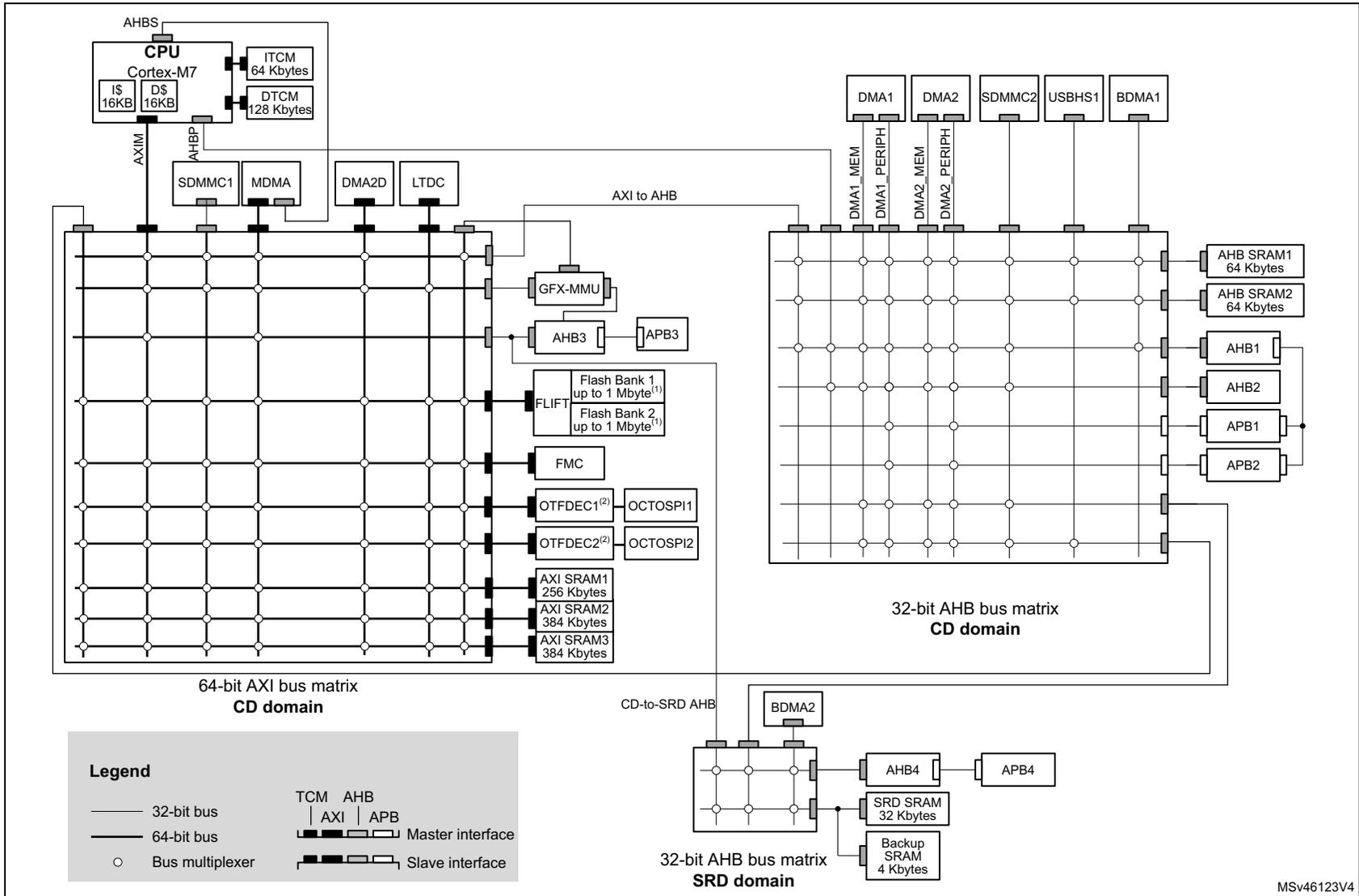
The diagram illustrates the system architecture for STM32H7A3/7B3/7B0xx devices, showing the interconnections between the CPU, memory, and various peripherals through a 32-bit AHB bus matrix.
CPU and Memory: The CPU (Cortex-M7) is connected to the AHBS bus. It includes I$ (16KB), D$ (16KB), ITCM (64 Kbytes), and DTCM (128 Kbytes). The CPU is connected to the AXI to AHB bridge via the AXI4 interface.
CD domain (Core Domain): The CD domain contains a 64-bit AXI bus matrix. It is connected to the CPU via the AXI4 interface and to the SRD domain via the CD-to-SRD AHB bridge. The matrix is connected to various peripherals and memory blocks:
- Peripherals: SDMMC1, MDMA, DMA2D, LTDC, GFX-MMU, AHB3, APB3, FLIFT (Flash Bank 1 up to 1 Mbyte 1 , Flash Bank 2 up to 1 Mbyte 1 ), FMC, OTFDEC1 2 (OCTOSPI1), OTFDEC2 2 (OCTOSPI2).
- Memory: AXI SRAM1 (256 Kbytes), AXI SRAM2 (384 Kbytes), AXI SRAM3 (384 Kbytes).
SRD domain (System Domain): The SRD domain contains a 32-bit AHB bus matrix. It is connected to the CD domain via the CD-to-SRD AHB bridge. The matrix is connected to various peripherals and memory blocks:
- Peripherals: DMA1, DMA2, SDMMC2, USBHS1, BDMA1, BDMA2, AHB4, APB4.
- Memory: AHB SRAM1 (64 Kbytes), AHB SRAM2 (64 Kbytes), AHB1, AHB2, APB1, APB2, SRD SRAM (32 Kbytes), Backup SRAM (4 Kbytes).
Legend:
- 32-bit bus (thin line)
- 64-bit bus (thick line)
- Bus multiplexer (circle)
- TCM: AXI (Master interface), AHB (Slave interface)
- AHB: AXI (Master interface), APB (Slave interface)
MSV46123V4
- 1. Bank 1 is limited to 128 Kbytes on STM32H7B0 devices. STM32H7A3xG and STM32H7A3xI/7B3xx devices feature two banks of 512 Kbytes and 1 Mbyte each, respectively.
- 2. OTFDEC1 and OTFDEC2 are available only on STM32H7B0 and STM32H7B3 devices.
2.1.1 Bus matrices
AXI bus matrix in CD domain
The CD domain multi AXI bus matrix ensures and arbitrates concurrent accesses from multiple masters to multiple slaves. This allows efficient simultaneous operation of high-speed peripherals.
The arbitration uses a round-robin algorithm with QoS capability.
Refer to Section 2.2: AXI interconnect matrix (AXIM) for more information on AXI interconnect.
AHB bus matrices in CD domain
The AHB bus matrices in CD domain ensure and arbitrate concurrent accesses from multiple masters to multiple slaves. This allows efficient simultaneous operation of high-speed peripherals.
The arbitration uses a round-robin algorithm.
2.1.2 TCM buses
The DTCM and ITCM (data and instruction tightly coupled RAMs) are connected through dedicated TCM buses directly to the Cortex-M7 core. The MDMA controller can access the DTCM and ITCM through AHBS, a specific CPU slave AHB. The ITCM is accessed by Cortex-M7 at CPU clock speed, with zero wait states.
2.1.3 Bus-to-bus bridges
To allow peripherals with different types of buses to communicate together, there is a number of bus-to-bus bridges in the system.
The AHB/APB bridges allow connecting peripherals on APB1 and APB2 to AHB1. Other bridges in the CD domain and in the SRD domain allow connecting APB3 to AHB3 and APB4 to AHB4, respectively. These AHB/APB bridges provide full synchronous interfacing, which allows the APB peripherals to operate with clocks independent of AHB that they connect to.
The AHB/APB bridges also allow APB1 and APB2 peripherals to connect to DMA1 and DMA2 peripheral buses, respectively, without transiting through AHB1.
The AHB/APB bridges convert 8-bit / 16-bit APB data to 32-bit AHB data, by replicating it to the three upper bytes / the upper half-word of the 32-bit word.
The AXI bus matrix incorporates AHB/AXI bus bridge functionality on its slave bus interfaces. The AXI/AHB bus bridges on its master interfaces marked as 32-bit in Figure 1 are outside the matrix.
The Cortex-M7 CPU provides AHB/TCM-bus (ITCM and DTCM buses) translation from its AHBS slave AHB, allowing the MDMA controller to access the ITCM and DTCM.
2.1.4 Domain and inter-domain buses
AXI to CD AHB
A 32-bit bus connects the AXI bus matrix to the AHB bus matrix. It allows AXI bus master to access resources (bus slaves) inside the CD domain.
CD AHB to AXI bus
A 32-bit bus connects the AHB bus matrix to the AXI bus matrix. It allows AHB bus masters to access resources (bus slaves) inside the CD domain and indirectly via the CD-to-SRD AHB in the SRD domain.
AXI to SRD AHB
This 32-bit bus connects the CD domain to the SRD domain AHB bus matrix. It allows bus masters in the CD domain to access resources (bus slaves) in the SRD domain.
CD AHB to SRD AHB
This 32-bit bus connects the CD domain to the SRD domain AHB bus matrix. It allows bus masters in the CD domain to access resources (bus slaves) in the SRD domain.
2.1.5 CPU buses
Cortex ® -M7 AXIM bus
The Cortex ® -M7 CPU uses the 64-bit AXIM bus to access all memories (excluding ITCM, and DTCM) and AHB3, AHB4, APB3 and APB4 peripherals (excluding AHB1, APB1 and APB2 peripherals).
The AXIM bus connects the CPU to the AXI bus matrix in the CD domain.
Cortex ® -M7 ITCM bus
The Cortex ® -M7 CPU uses the 64-bit ITCM bus for fetching instructions from and accessing data in the ITCM.
Cortex ® -M7 DTCM bus
The Cortex ® -M7 CPU uses the 2x32-bit DTCM bus for accessing data in the DTCM. The 2x32-bit DTCM bus allows load/load and load/store instruction pairs to be dual-issued on the DTCM memory. It can also fetch instructions.
Cortex ® -M7 AHBS bus
The Cortex ® -M7 CPU uses the 32-bit AHBS slave bus to allow the MDMA controller to access the ITCM and the DTCM.
Cortex ® -M7 AHBP bus
The Cortex ® -M7 CPU uses the 32-bit AHBP bus for accessing AHB1, AHB2, APB1 and APB2 peripherals via the AHB bus matrix in the CD domain.
2.1.6 Bus master peripherals
SDMMC1
The SDMMC1 uses a 32-bit bus, connected to the AXI bus matrix, through which it can access internal AXI SRAM and flash memories, and external memories through the OCTOSPI1/2 controllers and the FMC.
SDMMC2
The SDMMC2 uses a 32-bit bus, connected to the AHB bus matrix in CD domain. Through the system bus matrices, it can access the internal AXI SRAM1, AXI SRAM2, AXI SRAM3, AHB SRAM1, AHB SRAM2 and flash memories, and external memories through the OCTOSPI1/2 controllers and the FMC.
MDMA controller
The MDMA controller has two bus masters: an AXI 64-bit bus, connected to the AXI bus matrix and an AHB 32-bit bus connected to the Cortex-M7 AHBS slave bus.
The MDMA is optimized for DMA data transfers between memories since it supports linked list transfers that allow performing a chained list of transfers without the need for CPU intervention. Through the system bus matrices and the Cortex-M7 AHBS slave bus, the MDMA can access all internal and external memories through the OCTOSPI1/2 controllers and the FMC.
DMA1 and DMA2 controllers
The DMA1 and DMA2 controllers have two 32-bit buses - memory bus and peripheral bus, connected to the AHB bus matrix in CD domain.
The memory bus allows DMA data transfers between memories. Through the system bus matrices, the memory bus can access external memories through the OCTOSPI1/2 controllers and the FMC and all internal memories except ITCM and DTCM.
The peripheral bus allows DMA data transfers between two peripherals, between two memories or between a peripheral and a memory. Through the system bus matrices, the peripheral bus can access external memories through the OCTOSPI controller and the FMC, all AHB and APB peripherals and all internal memories except ITCM and DTCM. A direct access to APB1 and APB2 is available, without passing through AHB1. Direct path to APB1 and APB2 bridges allows reducing the bandwidth usage on AHB1 bus by improving data treatment efficiency for APB and AHB peripherals.
BDMA1 controller
The BDMA1 controller is connected to the AHB bus matrix in the CD domain. It is dedicated to the DFSDM1 which is connected to the APB2 bus. The BDMA1 allows DMA data transfers between the DFSDM and AHB SRAM or AHB1, APB1 and APB2 peripherals.
BDMA2 controller
The BDMA2 controller uses a 32-bit bus, connected to the AHB bus matrix in SRD domain, for DMA data transfers between two peripherals, between two memories or between a peripheral and a memory. BDMA2 transfers are limited to the SRD domain resources. It can access the internal SRD SRAM, backup SRAM, and AHB4 and APB4 peripherals through the AHB bus matrix in the SRD domain.
Chrom-Art Accelerator (DMA2D)
The DMA2D graphics accelerator uses a 64-bit bus, connected to the AXI bus matrix. Through the system bus matrices, internal AXI SRAM1, AXI SRAM2, AXI SRAM3, AHB SRAM1, AHB SRAM2 and flash memories, and external memories through the OCTOSPI1/2 controllers and the FMC.
LCD-TFT controller (LTDC)
The LCD-TFT display controller, LTDC, uses a 64-bit bus, connected to the AXI bus matrix, through which it can access internal AXI SRAM1, AXI SRAM2, AXI SRAM3 and flash memories, and external memories through the OCTOSPI1/2 controllers and the FMC.
OTG_HS peripheral
The OTG_HS peripheral uses a 32-bit bus, connected to the AHB bus matrix in the CD domain. Through the system bus matrix, it can access all internal memories except ITCM and DTCM, and external memories through the OCTOSPI1/2 controllers and the FMC.
2.1.7 Clocks to functional blocks
Upon reset, clocks to blocks such as peripherals and some memories are disabled (except for the SRAM, DTCM, ITCM and flash memory). To operate a block with no clock upon reset, the software must first enable its clock through RCC_AHBxENR or RCC_APBxENR register, respectively.
2.2 AXI interconnect matrix (AXIM)
2.2.1 AXI introduction
The AXI (advanced extensible interface) interconnect is based on the Arm® CoreLink™ NIC-400 Network Interconnect. The interconnect has seven initiator ports, or ASIBs (AMBA slave interface blocks), and ten target ports, or AMIBs (AMBA master interface blocks). The ASIBs are connected to the AMIBs via an AXI switch matrix.
Each ASIB is a slave on an AXI bus or AHB (advanced high-performance bus). Similarly, each AMIB is a master on an AXI or AHB bus. Where an ASIB or AMIB is connected to an AHB, it converts between the AHB and the AXI protocol.
The AXI interconnect includes a GPV (global programmer view) which contains registers for configuring certain parameters, such as the QoS (quality of service) level at each ASIB.
Any accesses to unallocated address space are handled by the default slave, which generates the return signals. This ensures that such transactions complete and do not block the issuing master and ASIB.
2.2.2 AXI interconnect main features
- • 64-bit AXI bus switch matrix with seven ASIBs and ten AMIBs, in CD domain
- • AHB/AXI bridge function built into the ASIBs
- • concurrent connectivity of multiple ASIBs to multiple AMIBs
- • programmable traffic priority management (QoS - quality of service)
- • software-configurable via GPV
2.2.3 AXI interconnect functional description
Block diagram
The AXI interconnect is shown in Figure 2 .
Figure 2. AXI interconnect
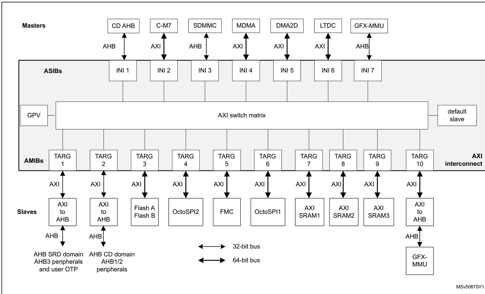
The diagram illustrates the AXI interconnect architecture. At the top, Masters are connected to the interconnect via ASIBs (AXI Slave Interface Blocks). The masters include CD AHB, C-M7, SDMMC, MDMA, DMA2D, LTDC, and GFX-MMU. The ASIBs are labeled INI 1 through INI 7. Below the ASIBs is the AXI switch matrix , which is also connected to a GPV (General Purpose Voltage) and a default slave . Below the switch matrix are AMIBs (AXI Master Interface Blocks), labeled TARG 1 through TARG 10. These are connected to various Slaves . The slaves include AXI to AHB (connected to AHB SRD domain and AHB3 peripherals and user OTP), AXI to AHB (connected to AHB CD domain and AHB1/2 peripherals), Flash A Flash B, OctoSPI2, FMC, OctoSPI1, AXI SRAM1, AXI SRAM2, AXI SRAM3, and another AXI to AHB (connected to GFX-MMU). The diagram also indicates bus widths: 32-bit bus and 64-bit bus.
MSV50670V1.
ASIB configuration
Table 3 summarizes the characteristics of the ASIBs.
Table 3. ASIB configuration
| ASIB | Connected master | Protocol | Bus width | R/W issuing |
|---|---|---|---|---|
| INI 1 | AHB from CD domain | AHB-lite | 32 | 1/4 |
| INI 2 | Cortex-M7 | AXI4 | 64 | 7/32 |
| INI 3 | SDMMC1 | AHB-lite | 32 | 1/4 |
| INI 4 | MDMA | AXI4 | 64 | 4/1 |
| INI 5 | DMA2D | AXI4 | 64 | 2/1 |
| INI 6 | LTDC | AXI4 | 64 | 2/1 |
| INI 7 | GFXMMU | AHB-lite | 32 | 1/1 |
AMIB configuration
Table 4 summarizes the characteristics of the AMIBs.
Table 4. AMIB configuration
| AMIB | Connected slave | Protocol | Bus width | R/W/Total acceptance |
|---|---|---|---|---|
| TARG 1 | Peripheral 3, SRD AHB and user OTP | AXI4 (1) | 32 | 1/1/1 |
| TARG 2 | CD AHB | AXI4 (1) | 32 | 1/1/1 |
| TARG 3 | Flash A and Flash B | AXI4 | 64 | 3/4/7 |
| TARG 4 | OCTOSPI2 | AXI4 | 64 | 3/2/5 |
| TARG 5 | FMC | AXI4 | 64 | 3/3/6 |
| TARG 6 | OCTOSPI1 | AXI4 | 64 | 2/1/3 |
| TARG 7 | AXI SRAM1 | AXI3 | 64 | 2/2/4 |
| TARG 8 | AXI SRAM2 | AXI3 | 64 | 2/2/4 |
| TARG 9 | AXI SRAM3 | AXI3 | 64 | 2/2/4 |
| TARG 10 | GFXMMU (1) | AXI4 | 32 | 2/2/4 |
- Conversion to AHB protocol is done via an AXI/AHB bridge sitting between AXI interconnect and the connected slave.
Quality of service (QoS)
The AXI switch matrix uses a priority-based arbitration when two ASIB simultaneously attempt to access the same AMIB. Each ASIB has programmable read channel and write channel priorities, known as QoS, from 0 to 15, such that the higher the value, the higher the priority. The read channel QoS value is programmed in the AXI interconnect - INI x read QoS register (AXI_INIx_READ_QOS) , and the write channel in the AXI interconnect - INI x write QoS register (AXI_INIx_WRITE_QOS) . The default QoS value for all channels is 0 (lowest priority).
If two coincident transactions arrive at the same AMIB, the higher priority transaction passes before the lower priority. If the two transactions have the same QoS value, then a least-recently-used (LRU) priority scheme is adopted.
The QoS values should be programmed according to the latency requirements for the application. Setting a higher priority for an ASIB ensures a lower latency for transactions initiated by the associated bus master. This can be useful for real-time-constrained tasks, such as graphics processing (LTDC, DMA2D). Assigning a high priority to masters that can make many and frequent accesses to the same slave (such as the Cortex-M7 CPU) can block access to that slave by other lower-priority masters.
Global programmer view (GPV)
The GPV contains configuration registers for the AXI interconnect (see Section 2.2.4 ). These registers are only accessible by the Cortex-M7 CPU.
2.2.4 AXI interconnect registers
AXI interconnect - peripheral ID4 register (AXI_PERIPH_ID_4)
Address offset: 0x1FD0
Reset value: 0x0000 0004
| 31 | 30 | 29 | 28 | 27 | 26 | 25 | 24 | 23 | 22 | 21 | 20 | 19 | 18 | 17 | 16 |
|---|---|---|---|---|---|---|---|---|---|---|---|---|---|---|---|
| Res. | Res. | Res. | Res. | Res. | Res. | Res. | Res. | Res. | Res. | Res. | Res. | Res. | Res. | Res. | Res. |
| 15 | 14 | 13 | 12 | 11 | 10 | 9 | 8 | 7 | 6 | 5 | 4 | 3 | 2 | 1 | 0 |
| Res. | Res. | Res. | Res. | Res. | Res. | Res. | Res. | 4KCOUNT[3:0] | JEP106CON[3:0] | ||||||
| r | r | r | r | r | r | r | r | ||||||||
Bits 31:8 Reserved, must be kept at reset value.
Bits 7:4 4KCOUNT[3:0] : Register file size
0x0: N/A
Bits 3:0 JEP106CON[3:0] : JEP106 continuation code
0x4: Arm ®
AXI interconnect - peripheral ID0 register (AXI_PERIPH_ID_0)
Address offset: 0x1FE0
Reset value: 0x0000 0000
| 31 | 30 | 29 | 28 | 27 | 26 | 25 | 24 | 23 | 22 | 21 | 20 | 19 | 18 | 17 | 16 |
|---|---|---|---|---|---|---|---|---|---|---|---|---|---|---|---|
| Res. | Res. | Res. | Res. | Res. | Res. | Res. | Res. | Res. | Res. | Res. | Res. | Res. | Res. | Res. | Res. |
| 15 | 14 | 13 | 12 | 11 | 10 | 9 | 8 | 7 | 6 | 5 | 4 | 3 | 2 | 1 | 0 |
| Res. | Res. | Res. | Res. | Res. | Res. | Res. | Res. | PARTNUM[7:0] | |||||||
| r | r | r | r | r | r | r | r | ||||||||
Bits 31:8 Reserved, must be kept at reset value.
Bits 7:0
PARTNUM[7:0]
: Peripheral part number bits 0 to 7
0x00: Part number = 0x400
AXI interconnect - peripheral ID1 register (AXI_PERIPH_ID_1)
Address offset: 0x1FE4
Reset value: 0x0000 00B4
| 31 | 30 | 29 | 28 | 27 | 26 | 25 | 24 | 23 | 22 | 21 | 20 | 19 | 18 | 17 | 16 |
|---|---|---|---|---|---|---|---|---|---|---|---|---|---|---|---|
| Res. | Res. | Res. | Res. | Res. | Res. | Res. | Res. | Res. | Res. | Res. | Res. | Res. | Res. | Res. | Res. |
| 15 | 14 | 13 | 12 | 11 | 10 | 9 | 8 | 7 | 6 | 5 | 4 | 3 | 2 | 1 | 0 |
| Res. | Res. | Res. | Res. | Res. | Res. | Res. | Res. | JEP106ID[3:0] | PARTNUM[11:8] | ||||||
| r | r | r | r | r | r | r | r | ||||||||
Bits 31:8 Reserved, must be kept at reset value.
Bits 7:4
JEP106ID[3:0]
: JEP106 identity bits 0 to 3
0xB: Arm® JEDEC code
Bits 3:0
PARTNUM[11:8]
: Peripheral part number bits 8 to 11
0x4: Part number = 0x400
AXI interconnect - peripheral ID2 register (AXI_PERIPH_ID_2)
Address offset: 0x1FE8
Reset value: 0x0000 002B
| 31 | 30 | 29 | 28 | 27 | 26 | 25 | 24 | 23 | 22 | 21 | 20 | 19 | 18 | 17 | 16 |
|---|---|---|---|---|---|---|---|---|---|---|---|---|---|---|---|
| Res. | Res. | Res. | Res. | Res. | Res. | Res. | Res. | Res. | Res. | Res. | Res. | Res. | Res. | Res. | Res. |
| 15 | 14 | 13 | 12 | 11 | 10 | 9 | 8 | 7 | 6 | 5 | 4 | 3 | 2 | 1 | 0 |
| Res. | Res. | Res. | Res. | Res. | Res. | Res. | Res. | REVISION[3:0] | JEDEC | JEP106ID[6:4] | |||||
| r | r | r | r | r | r | r | r | ||||||||
Bits 7:4
REVISION[3:0]
: Peripheral revision number
0x2: r0p2
Bit 3
JEDEC
: JEP106 code flag
0x1: JEDEC allocated code
Bits 2:0
JEP106ID[6:4]
: JEP106 Identity bits 4 to 6
0x3: Arm® JEDEC code
Address offset: 0x1FEC
Reset value: 0x0000 0000
| 31 | 30 | 29 | 28 | 27 | 26 | 25 | 24 | 23 | 22 | 21 | 20 | 19 | 18 | 17 | 16 |
|---|---|---|---|---|---|---|---|---|---|---|---|---|---|---|---|
| Res. | Res. | Res. | Res. | Res. | Res. | Res. | Res. | Res. | Res. | Res. | Res. | Res. | Res. | Res. | Res. |
| 15 | 14 | 13 | 12 | 11 | 10 | 9 | 8 | 7 | 6 | 5 | 4 | 3 | 2 | 1 | 0 |
| Res. | Res. | Res. | Res. | Res. | Res. | Res. | Res. | REV_AND[3:0] | CUST_MOD_NUM[3:0] | ||||||
| r | r | r | r | r | r | r | r | ||||||||
Bits 31:8 Reserved, must be kept at reset value.
Bits 7:4 REV_AND[3:0] : Customer version0: None
Bits 3:0 CUST_MOD_NUM[3:0] : Customer modification0: None
AXI interconnect - component ID0 register (AXI_COMP_ID_0)Address offset: 0x1FF0
Reset value: 0x0000 000D
| 31 | 30 | 29 | 28 | 27 | 26 | 25 | 24 | 23 | 22 | 21 | 20 | 19 | 18 | 17 | 16 |
|---|---|---|---|---|---|---|---|---|---|---|---|---|---|---|---|
| Res. | Res. | Res. | Res. | Res. | Res. | Res. | Res. | Res. | Res. | Res. | Res. | Res. | Res. | Res. | Res. |
| 15 | 14 | 13 | 12 | 11 | 10 | 9 | 8 | 7 | 6 | 5 | 4 | 3 | 2 | 1 | 0 |
| Res. | Res. | Res. | Res. | Res. | Res. | Res. | Res. | PREAMBLE[7:0] | |||||||
| r | r | r | r | r | r | r | r | ||||||||
Bits 31:8 Reserved, must be kept at reset value.
Bits 7:0 PREAMBLE[7:0] : Preamble bits 0 to 70xD: Common ID value
AXI interconnect - component ID1 register (AXI_COMP_ID_1)
Address offset: 0x1FF4
Reset value: 0x0000 00F0
| 31 | 30 | 29 | 28 | 27 | 26 | 25 | 24 | 23 | 22 | 21 | 20 | 19 | 18 | 17 | 16 |
|---|---|---|---|---|---|---|---|---|---|---|---|---|---|---|---|
| Res. | Res. | Res. | Res. | Res. | Res. | Res. | Res. | Res. | Res. | Res. | Res. | Res. | Res. | Res. | Res. |
| 15 | 14 | 13 | 12 | 11 | 10 | 9 | 8 | 7 | 6 | 5 | 4 | 3 | 2 | 1 | 0 |
| Res. | Res. | Res. | Res. | Res. | Res. | Res. | Res. | CLASS[3:0] | PREAMBLE[11:8] | ||||||
| r | r | r | r | r | r | r | r | ||||||||
Bits 31:8 Reserved, must be kept at reset value.
Bits 7:4 CLASS[3:0] : Component class
0xF: Generic IP component class
Bits 3:0 PREAMBLE[11:8] : Preamble bits 8 to 11
0x0: Common ID value
AXI interconnect - component ID2 register (AXI_COMP_ID_2)
Address offset: 0x1FF8
Reset value: 0x0000 0005
| 31 | 30 | 29 | 28 | 27 | 26 | 25 | 24 | 23 | 22 | 21 | 20 | 19 | 18 | 17 | 16 |
|---|---|---|---|---|---|---|---|---|---|---|---|---|---|---|---|
| Res. | Res. | Res. | Res. | Res. | Res. | Res. | Res. | Res. | Res. | Res. | Res. | Res. | Res. | Res. | Res. |
| 15 | 14 | 13 | 12 | 11 | 10 | 9 | 8 | 7 | 6 | 5 | 4 | 3 | 2 | 1 | 0 |
| Res. | Res. | Res. | Res. | Res. | Res. | Res. | Res. | PREAMBLE[19:12] | |||||||
| r | r | r | r | r | r | r | r | ||||||||
Bits 31:8 Reserved, must be kept at reset value.
Bits 7:0 PREAMBLE[19:12] : Preamble bits 12 to 19
0x05: Common ID value
AXI interconnect - component ID3 register (AXI_COMP_ID_3)
Address offset: 0x1FFC
Reset value: 0x0000 00B1
| 31 | 30 | 29 | 28 | 27 | 26 | 25 | 24 | 23 | 22 | 21 | 20 | 19 | 18 | 17 | 16 |
|---|---|---|---|---|---|---|---|---|---|---|---|---|---|---|---|
| Res. | Res. | Res. | Res. | Res. | Res. | Res. | Res. | Res. | Res. | Res. | Res. | Res. | Res. | Res. | Res. |
| 15 | 14 | 13 | 12 | 11 | 10 | 9 | 8 | 7 | 6 | 5 | 4 | 3 | 2 | 1 | 0 |
| Res. | Res. | Res. | Res. | Res. | Res. | Res. | Res. | PREAMBLE[27:20] | |||||||
| r | r | r | r | r | r | r | r | ||||||||
Bits 31:8 Reserved, must be kept at reset value.
Bits 7:0 PREAMBLE[27:20] : Preamble bits 20 to 27
0xB1: Common ID value
AXI interconnect - TARG x bus matrix issuing functionality register (AXI_TARGx_FN_MOD_ISS_BM)
Address offset: 0x1008 + 0x1000 * x, (x = 1 to 10)
Reset value: 0x0000 0000
| 31 | 30 | 29 | 28 | 27 | 26 | 25 | 24 | 23 | 22 | 21 | 20 | 19 | 18 | 17 | 16 |
|---|---|---|---|---|---|---|---|---|---|---|---|---|---|---|---|
| Res. | Res. | Res. | Res. | Res. | Res. | Res. | Res. | Res. | Res. | Res. | Res. | Res. | Res. | Res. | Res. |
| 15 | 14 | 13 | 12 | 11 | 10 | 9 | 8 | 7 | 6 | 5 | 4 | 3 | 2 | 1 | 0 |
| Res. | Res. | Res. | Res. | Res. | Res. | Res. | Res. | Res. | Res. | Res. | Res. | Res. | Res. | WRITE ISS OVERR IDE | READ ISS OVERR IDE |
| rw | rw |
Bits 31:2 Reserved, must be kept at reset value.
Bit 1 WRITE_ISS_OVERRIDE : Switch matrix write issuing override for target
0: Default issuing capability
1: Set switch matrix write issuing capability to 1 (see Table 4: AMIB configuration )
Bit 0 READ_ISS_OVERRIDE : Switch matrix read issuing override for target
0: Default issuing capability
1: Set switch matrix read issuing capability to 1 (see Table 4: AMIB configuration )
AXI interconnect - TARG x bus matrix functionality 2 register (AXI_TARGx_FN_MOD2)
Address offset: 0x1024 + 0x1000 * x, (x = 1, 2, 7 to 10)
Reset value: 0x0000 0000
| 31 | 30 | 29 | 28 | 27 | 26 | 25 | 24 | 23 | 22 | 21 | 20 | 19 | 18 | 17 | 16 |
|---|---|---|---|---|---|---|---|---|---|---|---|---|---|---|---|
| Res. | Res. | Res. | Res. | Res. | Res. | Res. | Res. | Res. | Res. | Res. | Res. | Res. | Res. | Res. | Res. |
| 15 | 14 | 13 | 12 | 11 | 10 | 9 | 8 | 7 | 6 | 5 | 4 | 3 | 2 | 1 | 0 |
| Res. | Res. | Res. | Res. | Res. | Res. | Res. | Res. | Res. | Res. | Res. | Res. | Res. | Res. | Res. | BYPASS_MERGE |
| rw |
Bits 31:1 Reserved, must be kept at reset value.
Bit 0 BYPASS_MERGE : Disable packing of beats to match the output data width. Unaligned transactions are not realigned to the input data word boundary.
0: Normal operation
1: Disable packing
AXI interconnect - TARG x long burst functionality modification register (AXI_TARGx_FN_MOD_LB)
Address offset: 0x102C + 0x1000 * x, (x = 1, 2, 10)
Reset value: 0x0000 0000
| 31 | 30 | 29 | 28 | 27 | 26 | 25 | 24 | 23 | 22 | 21 | 20 | 19 | 18 | 17 | 16 |
|---|---|---|---|---|---|---|---|---|---|---|---|---|---|---|---|
| Res. | Res. | Res. | Res. | Res. | Res. | Res. | Res. | Res. | Res. | Res. | Res. | Res. | Res. | Res. | Res. |
| 15 | 14 | 13 | 12 | 11 | 10 | 9 | 8 | 7 | 6 | 5 | 4 | 3 | 2 | 1 | 0 |
| Res. | Res. | Res. | Res. | Res. | Res. | Res. | Res. | Res. | Res. | Res. | Res. | Res. | Res. | Res. | FN_MOD_LB |
| rw |
Bits 31:1 Reserved, must be kept at reset value.
Bit 0 FN_MOD_LB : Controls burst breaking of long bursts
0: Long bursts can not be generated at the output of the ASIB
1: Long bursts can be generated at the output of the ASIB
AXI interconnect - TARG x issuing functionality modification register
(AXI_TARGx_FN_MOD)
Address offset: \( 0x1108 + 0x1000 * x \) , ( \( x = 1, 2, 7 \) to \( 10 \) )
Reset value: 0x0000 0000
| 31 | 30 | 29 | 28 | 27 | 26 | 25 | 24 | 23 | 22 | 21 | 20 | 19 | 18 | 17 | 16 |
|---|---|---|---|---|---|---|---|---|---|---|---|---|---|---|---|
| Res. | Res. | Res. | Res. | Res. | Res. | Res. | Res. | Res. | Res. | Res. | Res. | Res. | Res. | Res. | Res. |
| 15 | 14 | 13 | 12 | 11 | 10 | 9 | 8 | 7 | 6 | 5 | 4 | 3 | 2 | 1 | 0 |
| Res. | Res. | Res. | Res. | Res. | Res. | Res. | Res. | Res. | Res. | Res. | Res. | Res. | Res. | WRITE ISS OVERR IDE | READ ISS OVERR IDE |
| nw | nw |
Bits 31:2 Reserved, must be kept at reset value.
Bit 1 WRITE_ISS_OVERRIDE : Override AMIB write issuing capability
0: Default issuing capability
1: Force issuing capability to 1 (see Table 4: AMIB configuration )
Bit 0 READ_ISS_OVERRIDE : Override AMIB read issuing capability
0: Default issuing capability
1: Force issuing capability to 1 (see Table 4: AMIB configuration )
AXI interconnect - INI x functionality modification 2 register
(AXI_INIx_FN_MOD2)
Address offset: \( 0x41024 + 0x1000 * x \) , ( \( x = 1, 3, 7 \) )
Reset value: 0x0000 0000
| 31 | 30 | 29 | 28 | 27 | 26 | 25 | 24 | 23 | 22 | 21 | 20 | 19 | 18 | 17 | 16 |
|---|---|---|---|---|---|---|---|---|---|---|---|---|---|---|---|
| Res. | Res. | Res. | Res. | Res. | Res. | Res. | Res. | Res. | Res. | Res. | Res. | Res. | Res. | Res. | Res. |
| 15 | 14 | 13 | 12 | 11 | 10 | 9 | 8 | 7 | 6 | 5 | 4 | 3 | 2 | 1 | 0 |
| Res. | Res. | Res. | Res. | Res. | Res. | Res. | Res. | Res. | Res. | Res. | Res. | Res. | Res. | Res. | BYPASS S_MERGE |
| nw |
Bits 31:1 Reserved, must be kept at reset value.
Bit 0 BYPASS_MERGE : Disables alteration of transactions by the up-sizer unless required by the protocol
0: Normal operation
1: Transactions pass through unaltered where allowed
AXI interconnect - INI x AHB functionality modification register (AXI_INIx_FN_MOD_AHB)
Address offset: 0x41028 + 0x1000 * x, (x = 1, 3, 7)
Reset value: 0x0000 0000
| 31 | 30 | 29 | 28 | 27 | 26 | 25 | 24 | 23 | 22 | 21 | 20 | 19 | 18 | 17 | 16 |
|---|---|---|---|---|---|---|---|---|---|---|---|---|---|---|---|
| Res. | Res. | Res. | Res. | Res. | Res. | Res. | Res. | Res. | Res. | Res. | Res. | Res. | Res. | Res. | Res. |
| 15 | 14 | 13 | 12 | 11 | 10 | 9 | 8 | 7 | 6 | 5 | 4 | 3 | 2 | 1 | 0 |
| Res. | Res. | Res. | Res. | Res. | Res. | Res. | Res. | Res. | Res. | Res. | Res. | Res. | Res. | WR_IN C_OVE RRIDE | RD_IN C_OVE RRIDE |
| rw | rw |
Bits 31:2 Reserved, must be kept at reset value.
Bit 1 WR_INC_OVERRIDE : Converts all AHB-Lite read transactions to a series of single beat AXI transactions; each AHB-Lite write beat is acknowledged with the AXI buffered write response.
- 0: Override disabled
- 1: Override enabled
Bit 0 RD_INC_OVERRIDE : Converts all AHB-Lite write transactions to a series of single beat AXI transactions
- 0: Override disabled
- 1: Override enabled
AXI interconnect - INI x read QoS register (AXI_INIx_READ_QOS)
Address offset: 0x41100 + 0x1000 * x, (x = 1 to 7)
Reset value: 0x0000 0000
| 31 | 30 | 29 | 28 | 27 | 26 | 25 | 24 | 23 | 22 | 21 | 20 | 19 | 18 | 17 | 16 |
|---|---|---|---|---|---|---|---|---|---|---|---|---|---|---|---|
| Res. | Res. | Res. | Res. | Res. | Res. | Res. | Res. | Res. | Res. | Res. | Res. | Res. | Res. | Res. | Res. |
| 15 | 14 | 13 | 12 | 11 | 10 | 9 | 8 | 7 | 6 | 5 | 4 | 3 | 2 | 1 | 0 |
| Res. | Res. | Res. | Res. | Res. | Res. | Res. | Res. | Res. | Res. | Res. | Res. | AR_QOS[3:0] | |||
| rw | rw | rw | rw | ||||||||||||
Bits 31:4 Reserved, must be kept at reset value.
Bits 3:0 AR_QOS[3:0] : Read channel QoS setting
- 0x0: Lowest priority
- 0xF: Highest priority
AXI interconnect - INI x write QoS register (AXI_INIx_WRITE_QOS)
Address offset: \( 0x41104 + 0x1000 * x \) , ( \( x = 1 \) to \( 7 \) )
Reset value: \( 0x0000\ 0000 \)
| 31 | 30 | 29 | 28 | 27 | 26 | 25 | 24 | 23 | 22 | 21 | 20 | 19 | 18 | 17 | 16 |
|---|---|---|---|---|---|---|---|---|---|---|---|---|---|---|---|
| Res. | Res. | Res. | Res. | Res. | Res. | Res. | Res. | Res. | Res. | Res. | Res. | Res. | Res. | Res. | Res. |
| 15 | 14 | 13 | 12 | 11 | 10 | 9 | 8 | 7 | 6 | 5 | 4 | 3 | 2 | 1 | 0 |
| Res. | Res. | Res. | Res. | Res. | Res. | Res. | Res. | Res. | Res. | Res. | Res. | AW_QOS[3:0] | |||
| rw | rw | rw | rw | ||||||||||||
Bits 31:4 Reserved, must be kept at reset value.
Bits 3:0 AW_QOS[3:0] : Write channel QoS setting
0x0: Lowest priority
0xF: Highest priority
AXI interconnect - INI x issuing functionality modification register (AXI_INIx_FN_MOD)
Address offset: \( 0x41108 + 0x1000 * x \) , ( \( x = 1 \) to \( 7 \) )
Reset value: \( 0x0000\ 0000 \)
| 31 | 30 | 29 | 28 | 27 | 26 | 25 | 24 | 23 | 22 | 21 | 20 | 19 | 18 | 17 | 16 |
|---|---|---|---|---|---|---|---|---|---|---|---|---|---|---|---|
| Res. | Res. | Res. | Res. | Res. | Res. | Res. | Res. | Res. | Res. | Res. | Res. | Res. | Res. | Res. | Res. |
| 15 | 14 | 13 | 12 | 11 | 10 | 9 | 8 | 7 | 6 | 5 | 4 | 3 | 2 | 1 | 0 |
| Res. | Res. | Res. | Res. | Res. | Res. | Res. | Res. | Res. | Res. | Res. | Res. | Res. | Res. | WRITE ISS OVERR IDE | READ ISS OVERR IDE |
| rw | rw |
Bits 31:2 Reserved, must be kept at reset value.
Bit 1 WRITE_ISS_OVERRIDE : Override ASIB write issuing capability
0: Normal issuing capability
1: Force issuing capability to 1
Bit 0 READ_ISS_OVERRIDE : Override ASIB read issuing capability
0: Normal issuing capability
1: Force issuing capability to 1
2.2.5 AXI interconnect register map
Table 5. AXI interconnect register map and reset values
| Offset | Register name | 31 | 30 | 29 | 28 | 27 | 26 | 25 | 24 | 23 | 22 | 21 | 20 | 19 | 18 | 17 | 16 | 15 | 14 | 13 | 12 | 11 | 10 | 9 | 8 | 7 | 6 | 5 | 4 | 3 | 2 | 1 | 0 |
|---|---|---|---|---|---|---|---|---|---|---|---|---|---|---|---|---|---|---|---|---|---|---|---|---|---|---|---|---|---|---|---|---|---|
| 0x1FD0 | AXI_PERIPH_ID_4 | Res. | Res. | Res. | Res. | Res. | Res. | Res. | Res. | Res. | Res. | Res. | Res. | Res. | Res. | Res. | Res. | Res. | Res. | Res. | Res. | Res. | Res. | Res. | Res. | 4KCOUNT [3:0] | JEP106CON [3:0] | ||||||
| Reset value | 0 | 0 | 0 | 0 | 0 | 1 | 0 | 0 | |||||||||||||||||||||||||
| 0x1FD4 | AXI_PERIPH_ID_5 | Res. | Res. | Res. | Res. | Res. | Res. | Res. | Res. | Res. | Res. | Res. | Res. | Res. | Res. | Res. | Res. | Res. | Res. | Res. | Res. | Res. | Res. | Res. | Res. | Reserved | |||||||
| Reset value | 0 | 0 | 0 | 0 | 0 | 0 | 0 | 0 | |||||||||||||||||||||||||
| 0x1FD8 | AXI_PERIPH_ID_6 | Res. | Res. | Res. | Res. | Res. | Res. | Res. | Res. | Res. | Res. | Res. | Res. | Res. | Res. | Res. | Res. | Res. | Res. | Res. | Res. | Res. | Res. | Res. | Res. | Reserved | |||||||
| Reset value | 0 | 0 | 0 | 0 | 0 | 0 | 0 | 0 | |||||||||||||||||||||||||
| 0x1FDC | AXI_PERIPH_ID_7 | Res. | Res. | Res. | Res. | Res. | Res. | Res. | Res. | Res. | Res. | Res. | Res. | Res. | Res. | Res. | Res. | Res. | Res. | Res. | Res. | Res. | Res. | Res. | Res. | Reserved | |||||||
| Reset value | 0 | 0 | 0 | 0 | 0 | 0 | 0 | 0 | |||||||||||||||||||||||||
| 0x1FE0 | AXI_PERIPH_ID_0 | Res. | Res. | Res. | Res. | Res. | Res. | Res. | Res. | Res. | Res. | Res. | Res. | Res. | Res. | Res. | Res. | Res. | Res. | Res. | Res. | Res. | Res. | Res. | Res. | PARTNUM[7:0] | |||||||
| Reset value | 0 | 0 | 0 | 0 | 0 | 0 | 0 | 0 | |||||||||||||||||||||||||
| 0x1FE4 | AXI_PERIPH_ID_1 | Res. | Res. | Res. | Res. | Res. | Res. | Res. | Res. | Res. | Res. | Res. | Res. | Res. | Res. | Res. | Res. | Res. | Res. | Res. | Res. | Res. | Res. | Res. | Res. | JEP106ID [3:0] | PARTNUM [11:8] | ||||||
| Reset value | 1 | 0 | 1 | 1 | 0 | 1 | 0 | 0 | |||||||||||||||||||||||||
| 0x1FE8 | AXI_PERIPH_ID_2 | Res. | Res. | Res. | Res. | Res. | Res. | Res. | Res. | Res. | Res. | Res. | Res. | Res. | Res. | Res. | Res. | Res. | Res. | Res. | Res. | Res. | Res. | Res. | Res. | REVISION [3:0] | JEDEC | JEP106ID [6:4] | |||||
| Reset value | 0 | 0 | 1 | 0 | 1 | 0 | 1 | 1 | |||||||||||||||||||||||||
| 0x1FEC | AXI_PERIPH_ID_3 | Res. | Res. | Res. | Res. | Res. | Res. | Res. | Res. | Res. | Res. | Res. | Res. | Res. | Res. | Res. | Res. | Res. | Res. | Res. | Res. | Res. | Res. | Res. | Res. | REV_AND[3:0] | CUST_MOD_NUM [3:0] | ||||||
| Reset value | 0 | 0 | 0 | 0 | 0 | 0 | 0 | 0 | |||||||||||||||||||||||||
| 0x1FF0 | AXI_COMP_ID_0 | Res. | Res. | Res. | Res. | Res. | Res. | Res. | Res. | Res. | Res. | Res. | Res. | Res. | Res. | Res. | Res. | Res. | Res. | Res. | Res. | Res. | Res. | Res. | Res. | PREAMBLE[7:0] | |||||||
| Reset value | 0 | 0 | 0 | 0 | 1 | 1 | 0 | 1 | |||||||||||||||||||||||||
| 0x1FF4 | AXI_COMP_ID_1 | Res. | Res. | Res. | Res. | Res. | Res. | Res. | Res. | Res. | Res. | Res. | Res. | Res. | Res. | Res. | Res. | Res. | Res. | Res. | Res. | Res. | Res. | Res. | Res. | CLASS[3:0] | PREAMBLE [11:8] | ||||||
| Reset value | 1 | 1 | 1 | 1 | 0 | 0 | 0 | 0 | |||||||||||||||||||||||||
Table 5. AXI interconnect register map and reset values (continued)
| Offset | Register name | 31 | 30 | 29 | 28 | 27 | 26 | 25 | 24 | 23 | 22 | 21 | 20 | 19 | 18 | 17 | 16 | 15 | 14 | 13 | 12 | 11 | 10 | 9 | 8 | 7 | 6 | 5 | 4 | 3 | 2 | 1 | 0 |
|---|---|---|---|---|---|---|---|---|---|---|---|---|---|---|---|---|---|---|---|---|---|---|---|---|---|---|---|---|---|---|---|---|---|
| 0x1FF8 | AXI_COMP_ID_2 | Res. | PREAMBLE[19:12] | ||||||||||||||||||||||||||||||
| Reset value | 0 | 0 | 0 | 0 | 0 | 1 | 0 | 1 | |||||||||||||||||||||||||
| 0x1FFC | AXI_COMP_ID_3 | Res. | PREAMBLE[27:20] | ||||||||||||||||||||||||||||||
| Reset value | 1 | 0 | 1 | 1 | 0 | 0 | 0 | 1 | |||||||||||||||||||||||||
| 0x2000 - 0x2004 | Reserved | Res. | Res. | Res. | Res. | Res. | Res. | Res. | Res. | Res. | Res. | Res. | Res. | Res. | Res. | Res. | Res. | Res. | Res. | Res. | Res. | Res. | Res. | Res. | Res. | Res. | Res. | Res. | Res. | Res. | Res. | Res. | Res. |
| 0x2008 | AXI_TARG1_FN_MOD_ISS_BM | Res. | WRITE_ISS_OVERRIDE | READ_ISS_OVERRIDE | |||||||||||||||||||||||||||||
| Reset value | 0 | 0 | |||||||||||||||||||||||||||||||
| 0x200C - 0x2020 | Reserved | Res. | Res. | Res. | Res. | Res. | Res. | Res. | Res. | Res. | Res. | Res. | Res. | Res. | Res. | Res. | Res. | Res. | Res. | Res. | Res. | Res. | Res. | Res. | Res. | Res. | Res. | Res. | Res. | Res. | Res. | Res. | Res. |
| 0x2024 | AXI_TARG1_FN_MOD2 | Res. | BYPASS_MERGE | ||||||||||||||||||||||||||||||
| Reset value | 0 | ||||||||||||||||||||||||||||||||
| 0x2028 | Reserved | Res. | Res. | Res. | Res. | Res. | Res. | Res. | Res. | Res. | Res. | Res. | Res. | Res. | Res. | Res. | Res. | Res. | Res. | Res. | Res. | Res. | Res. | Res. | Res. | Res. | Res. | Res. | Res. | Res. | Res. | Res. | Res. |
| 0x202C | AXI_TARG1_FN_MOD_LB | Res. | FN_MOD_LB | ||||||||||||||||||||||||||||||
| Reset value | 0 | ||||||||||||||||||||||||||||||||
| 0x2030 - 0x2104 | Reserved | Res. | Res. | Res. | Res. | Res. | Res. | Res. | Res. | Res. | Res. | Res. | Res. | Res. | Res. | Res. | Res. | Res. | Res. | Res. | Res. | Res. | Res. | Res. | Res. | Res. | Res. | Res. | Res. | Res. | Res. | Res. | Res. |
| 0x2108 | AXI_TARG1_FN_MOD | Res. | WRITE_ISS_OVERRIDE | READ_ISS_OVERRIDE | |||||||||||||||||||||||||||||
| Reset value | 0 | 0 | |||||||||||||||||||||||||||||||
| 0x210C - 0x3004 | Reserved | Res. | Res. | Res. | Res. | Res. | Res. | Res. | Res. | Res. | Res. | Res. | Res. | Res. | Res. | Res. | Res. | Res. | Res. | Res. | Res. | Res. | Res. | Res. | Res. | Res. | Res. | Res. | Res. | Res. | Res. | Res. | Res. |
Table 5. AXI interconnect register map and reset values (continued)
| Offset | Register name | 31 | 30 | 29 | 28 | 27 | 26 | 25 | 24 | 23 | 22 | 21 | 20 | 19 | 18 | 17 | 16 | 15 | 14 | 13 | 12 | 11 | 10 | 9 | 8 | 7 | 6 | 5 | 4 | 3 | 2 | 1 | 0 |
|---|---|---|---|---|---|---|---|---|---|---|---|---|---|---|---|---|---|---|---|---|---|---|---|---|---|---|---|---|---|---|---|---|---|
| 0x3008 | AXI_TARG2_ FN_MOD_ ISS_BM | Res. | Res. | Res. | Res. | Res. | Res. | Res. | Res. | Res. | Res. | Res. | Res. | Res. | Res. | Res. | Res. | Res. | Res. | Res. | Res. | Res. | Res. | Res. | Res. | Res. | Res. | Res. | Res. | Res. | Res. | WRITE_ISS_OVERRIDE | READ_ISS_OVERRIDE |
| Reset value | 0 | 0 | |||||||||||||||||||||||||||||||
| 0x300C - 0x3020 | Reserved | Res. | Res. | Res. | Res. | Res. | Res. | Res. | Res. | Res. | Res. | Res. | Res. | Res. | Res. | Res. | Res. | Res. | Res. | Res. | Res. | Res. | Res. | Res. | Res. | Res. | Res. | Res. | Res. | Res. | Res. | Res. | Res. |
| 0x3024 | AXI_TARG2_ FN_MOD2 | Res. | Res. | Res. | Res. | Res. | Res. | Res. | Res. | Res. | Res. | Res. | Res. | Res. | Res. | Res. | Res. | Res. | Res. | Res. | Res. | Res. | Res. | Res. | Res. | Res. | Res. | Res. | Res. | Res. | Res. | Res. | BYPASS_MERGE |
| Reset value | 0 | ||||||||||||||||||||||||||||||||
| 0x3028 | Reserved | Res. | Res. | Res. | Res. | Res. | Res. | Res. | Res. | Res. | Res. | Res. | Res. | Res. | Res. | Res. | Res. | Res. | Res. | Res. | Res. | Res. | Res. | Res. | Res. | Res. | Res. | Res. | Res. | Res. | Res. | Res. | Res. |
| 0x302C | AXI_TARG2_ FN_MOD_LB | Res. | Res. | Res. | Res. | Res. | Res. | Res. | Res. | Res. | Res. | Res. | Res. | Res. | Res. | Res. | Res. | Res. | Res. | Res. | Res. | Res. | Res. | Res. | Res. | Res. | Res. | Res. | Res. | Res. | Res. | Res. | FN_MOD_LB |
| Reset value | 0 | ||||||||||||||||||||||||||||||||
| 0x3030 - 0x3104 | Reserved | Res. | Res. | Res. | Res. | Res. | Res. | Res. | Res. | Res. | Res. | Res. | Res. | Res. | Res. | Res. | Res. | Res. | Res. | Res. | Res. | Res. | Res. | Res. | Res. | Res. | Res. | Res. | Res. | Res. | Res. | Res. | Res. |
| 0x3108 | AXI_TARG2_ FN_MOD | Res. | Res. | Res. | Res. | Res. | Res. | Res. | Res. | Res. | Res. | Res. | Res. | Res. | Res. | Res. | Res. | Res. | Res. | Res. | Res. | Res. | Res. | Res. | Res. | Res. | Res. | Res. | Res. | Res. | Res. | WRITE_ISS_OVERRIDE | READ_ISS_OVERRIDE |
| Reset value | 0 | 0 | |||||||||||||||||||||||||||||||
| 0x310C - 0x4004 | Reserved | Res. | Res. | Res. | Res. | Res. | Res. | Res. | Res. | Res. | Res. | Res. | Res. | Res. | Res. | Res. | Res. | Res. | Res. | Res. | Res. | Res. | Res. | Res. | Res. | Res. | Res. | Res. | Res. | Res. | Res. | Res. | Res. |
| 0x4008 | AXI_TARG3_ FN_MOD_ ISS_BM | Res. | Res. | Res. | Res. | Res. | Res. | Res. | Res. | Res. | Res. | Res. | Res. | Res. | Res. | Res. | Res. | Res. | Res. | Res. | Res. | Res. | Res. | Res. | Res. | Res. | Res. | Res. | Res. | Res. | Res. | WRITE_ISS_OVERRIDE | READ_ISS_OVERRIDE |
| Reset value | 0 | 0 | |||||||||||||||||||||||||||||||
| 0x400C - 0x5004 | Reserved | Res. | Res. | Res. | Res. | Res. | Res. | Res. | Res. | Res. | Res. | Res. | Res. | Res. | Res. | Res. | Res. | Res. | Res. | Res. | Res. | Res. | Res. | Res. | Res. | Res. | Res. | Res. | Res. | Res. | Res. | Res. | Res. |
Table 5. AXI interconnect register map and reset values (continued)
| Offset | Register name | 31 | 30 | 29 | 28 | 27 | 26 | 25 | 24 | 23 | 22 | 21 | 20 | 19 | 18 | 17 | 16 | 15 | 14 | 13 | 12 | 11 | 10 | 9 | 8 | 7 | 6 | 5 | 4 | 3 | 2 | 1 | 0 | |
|---|---|---|---|---|---|---|---|---|---|---|---|---|---|---|---|---|---|---|---|---|---|---|---|---|---|---|---|---|---|---|---|---|---|---|
| 0x5008 | AXI_TARG4_ FN_MOD_ ISS_BM | Res. | Res. | Res. | Res. | Res. | Res. | Res. | Res. | Res. | Res. | Res. | Res. | Res. | Res. | Res. | Res. | Res. | Res. | Res. | Res. | Res. | Res. | Res. | Res. | Res. | Res. | Res. | Res. | Res. | Res. | WRITE_ISS_OVERRIDE | READ_ISS_OVERRIDE | |
| Reset value | 0 | 0 | ||||||||||||||||||||||||||||||||
| 0x500C - 0x6004 | Reserved | Res. | Res. | Res. | Res. | Res. | Res. | Res. | Res. | Res. | Res. | Res. | Res. | Res. | Res. | Res. | Res. | Res. | Res. | Res. | Res. | Res. | Res. | Res. | Res. | Res. | Res. | Res. | Res. | Res. | Res. | Res. | Res. | |
| 0x6008 | AXI_TARG5_ FN_MOD_ ISS_BM | Res. | Res. | Res. | Res. | Res. | Res. | Res. | Res. | Res. | Res. | Res. | Res. | Res. | Res. | Res. | Res. | Res. | Res. | Res. | Res. | Res. | Res. | Res. | Res. | Res. | Res. | Res. | Res. | Res. | Res. | WRITE_ISS_OVERRIDE | READ_ISS_OVERRIDE | |
| Reset value | 0 | 0 | ||||||||||||||||||||||||||||||||
| 0x600C - 0x7004 | Reserved | Res. | Res. | Res. | Res. | Res. | Res. | Res. | Res. | Res. | Res. | Res. | Res. | Res. | Res. | Res. | Res. | Res. | Res. | Res. | Res. | Res. | Res. | Res. | Res. | Res. | Res. | Res. | Res. | Res. | Res. | Res. | Res. | |
| 0x7008 | AXI_TARG6_ FN_MOD_ ISS_BM | Res. | Res. | Res. | Res. | Res. | Res. | Res. | Res. | Res. | Res. | Res. | Res. | Res. | Res. | Res. | Res. | Res. | Res. | Res. | Res. | Res. | Res. | Res. | Res. | Res. | Res. | Res. | Res. | Res. | Res. | WRITE_ISS_OVERRIDE | READ_ISS_OVERRIDE | |
| Reset value | 0 | 0 | ||||||||||||||||||||||||||||||||
| 0x700C - 0x8004 | Reserved | Res. | Res. | Res. | Res. | Res. | Res. | Res. | Res. | Res. | Res. | Res. | Res. | Res. | Res. | Res. | Res. | Res. | Res. | Res. | Res. | Res. | Res. | Res. | Res. | Res. | Res. | Res. | Res. | Res. | Res. | Res. | Res. | |
| 0x8008 | AXI_TARG7_ FN_MOD_ ISS_BM | Res. | Res. | Res. | Res. | Res. | Res. | Res. | Res. | Res. | Res. | Res. | Res. | Res. | Res. | Res. | Res. | Res. | Res. | Res. | Res. | Res. | Res. | Res. | Res. | Res. | Res. | Res. | Res. | Res. | Res. | WRITE_ISS_OVERRIDE | READ_ISS_OVERRIDE | |
| Reset value | 0 | 0 | ||||||||||||||||||||||||||||||||
| 0x800C - 0x8020 | Reserved | Res. | Res. | Res. | Res. | Res. | Res. | Res. | Res. | Res. | Res. | Res. | Res. | Res. | Res. | Res. | Res. | Res. | Res. | Res. | Res. | Res. | Res. | Res. | Res. | Res. | Res. | Res. | Res. | Res. | Res. | Res. | Res. | |
| 0x8024 | AXI_TARG7_ FN_MOD2 | Res. | Res. | Res. | Res. | Res. | Res. | Res. | Res. | Res. | Res. | Res. | Res. | Res. | Res. | Res. | Res. | Res. | Res. | Res. | Res. | Res. | Res. | Res. | Res. | Res. | Res. | Res. | Res. | Res. | Res. | Res. | Res. | BYPASS_MERGE |
| Reset value | 0 |
Table 5. AXI interconnect register map and reset values (continued)
| Offset | Register name | 31 | 30 | 29 | 28 | 27 | 26 | 25 | 24 | 23 | 22 | 21 | 20 | 19 | 18 | 17 | 16 | 15 | 14 | 13 | 12 | 11 | 10 | 9 | 8 | 7 | 6 | 5 | 4 | 3 | 2 | 1 | 0 |
|---|---|---|---|---|---|---|---|---|---|---|---|---|---|---|---|---|---|---|---|---|---|---|---|---|---|---|---|---|---|---|---|---|---|
| 0x8028 - 0x8104 | Reserved | Res. | Res. | Res. | Res. | Res. | Res. | Res. | Res. | Res. | Res. | Res. | Res. | Res. | Res. | Res. | Res. | Res. | Res. | Res. | Res. | Res. | Res. | Res. | Res. | Res. | Res. | Res. | Res. | Res. | Res. | Res. | Res. |
| 0x8108 | AXI_TARG7_ FN_MOD | Res. | Res. | Res. | Res. | Res. | Res. | Res. | Res. | Res. | Res. | Res. | Res. | Res. | Res. | Res. | Res. | Res. | Res. | Res. | Res. | Res. | Res. | Res. | Res. | Res. | Res. | Res. | Res. | Res. | Res. | WRITE_ISS_OVERRIDE | READ_ISS_OVERRIDE |
| Reset value | 0 | 0 | |||||||||||||||||||||||||||||||
| 0x810C - 0x9004 | Reserved | Res. | Res. | Res. | Res. | Res. | Res. | Res. | Res. | Res. | Res. | Res. | Res. | Res. | Res. | Res. | Res. | Res. | Res. | Res. | Res. | Res. | Res. | Res. | Res. | Res. | Res. | Res. | Res. | Res. | Res. | Res. | Res. |
| 0x9008 | AXI_TARG8_ FN_MOD_ ISS_BM | Res. | Res. | Res. | Res. | Res. | Res. | Res. | Res. | Res. | Res. | Res. | Res. | Res. | Res. | Res. | Res. | Res. | Res. | Res. | Res. | Res. | Res. | Res. | Res. | Res. | Res. | Res. | Res. | Res. | Res. | WRITE_ISS_OVERRIDE | READ_ISS_OVERRIDE |
| Reset value | 0 | 0 | |||||||||||||||||||||||||||||||
| 0x900C - 0x9020 | Reserved | Res. | Res. | Res. | Res. | Res. | Res. | Res. | Res. | Res. | Res. | Res. | Res. | Res. | Res. | Res. | Res. | Res. | Res. | Res. | Res. | Res. | Res. | Res. | Res. | Res. | Res. | Res. | Res. | Res. | Res. | Res. | Res. |
| 0x9024 | AXI_TARG8_ FN_MOD2 | Res. | Res. | Res. | Res. | Res. | Res. | Res. | Res. | Res. | Res. | Res. | Res. | Res. | Res. | Res. | Res. | Res. | Res. | Res. | Res. | Res. | Res. | Res. | Res. | Res. | Res. | Res. | Res. | Res. | Res. | Res. | BYPASS_MERGE |
| Reset value | 0 | ||||||||||||||||||||||||||||||||
| 0x9028 - 0x9104 | Reserved | Res. | Res. | Res. | Res. | Res. | Res. | Res. | Res. | Res. | Res. | Res. | Res. | Res. | Res. | Res. | Res. | Res. | Res. | Res. | Res. | Res. | Res. | Res. | Res. | Res. | Res. | Res. | Res. | Res. | Res. | Res. | Res. |
| 0x9108 | AXI_TARG8_ FN_MOD | Res. | Res. | Res. | Res. | Res. | Res. | Res. | Res. | Res. | Res. | Res. | Res. | Res. | Res. | Res. | Res. | Res. | Res. | Res. | Res. | Res. | Res. | Res. | Res. | Res. | Res. | Res. | Res. | Res. | Res. | WRITE_ISS_OVERRIDE | READ_ISS_OVERRIDE |
| Reset value | 0 | 0 | |||||||||||||||||||||||||||||||
| 0x910C - 0xA004 | Reserved | Res. | Res. | Res. | Res. | Res. | Res. | Res. | Res. | Res. | Res. | Res. | Res. | Res. | Res. | Res. | Res. | Res. | Res. | Res. | Res. | Res. | Res. | Res. | Res. | Res. | Res. | Res. | Res. | Res. | Res. | Res. | Res. |
Table 5. AXI interconnect register map and reset values (continued)
| Offset | Register name | 31 | 30 | 29 | 28 | 27 | 26 | 25 | 24 | 23 | 22 | 21 | 20 | 19 | 18 | 17 | 16 | 15 | 14 | 13 | 12 | 11 | 10 | 9 | 8 | 7 | 6 | 5 | 4 | 3 | 2 | 1 | 0 |
|---|---|---|---|---|---|---|---|---|---|---|---|---|---|---|---|---|---|---|---|---|---|---|---|---|---|---|---|---|---|---|---|---|---|
| 0xA008 | AXI_TARG9_ FN_MOD_ ISS_BM | Res. | Res. | Res. | Res. | Res. | Res. | Res. | Res. | Res. | Res. | Res. | Res. | Res. | Res. | Res. | Res. | Res. | Res. | Res. | Res. | Res. | Res. | Res. | Res. | Res. | Res. | Res. | Res. | Res. | Res. | WRITE_ISS_OVERRIDE | READ_ISS_OVERRIDE |
| Reset value | 0 | 0 | |||||||||||||||||||||||||||||||
| 0xA00C - 0xA020 | Reserved | Res. | Res. | Res. | Res. | Res. | Res. | Res. | Res. | Res. | Res. | Res. | Res. | Res. | Res. | Res. | Res. | Res. | Res. | Res. | Res. | Res. | Res. | Res. | Res. | Res. | Res. | Res. | Res. | Res. | Res. | Res. | Res. |
| 0xA024 | AXI_TARG9_ FN_MOD2 | Res. | Res. | Res. | Res. | Res. | Res. | Res. | Res. | Res. | Res. | Res. | Res. | Res. | Res. | Res. | Res. | Res. | Res. | Res. | Res. | Res. | Res. | Res. | Res. | Res. | Res. | Res. | Res. | Res. | Res. | Res. | BYPASS_MERGE |
| Reset value | 0 | ||||||||||||||||||||||||||||||||
| 0xA028 - 0xA104 | Reserved | Res. | Res. | Res. | Res. | Res. | Res. | Res. | Res. | Res. | Res. | Res. | Res. | Res. | Res. | Res. | Res. | Res. | Res. | Res. | Res. | Res. | Res. | Res. | Res. | Res. | Res. | Res. | Res. | Res. | Res. | Res. | Res. |
| 0xA108 | AXI_TARG9_ FN_MOD | Res. | Res. | Res. | Res. | Res. | Res. | Res. | Res. | Res. | Res. | Res. | Res. | Res. | Res. | Res. | Res. | Res. | Res. | Res. | Res. | Res. | Res. | Res. | Res. | Res. | Res. | Res. | Res. | Res. | Res. | WRITE_ISS_OVERRIDE | READ_ISS_OVERRIDE |
| Reset value | 0 | 0 | |||||||||||||||||||||||||||||||
| 0xA10C - 0xB004 | Reserved | Res. | Res. | Res. | Res. | Res. | Res. | Res. | Res. | Res. | Res. | Res. | Res. | Res. | Res. | Res. | Res. | Res. | Res. | Res. | Res. | Res. | Res. | Res. | Res. | Res. | Res. | Res. | Res. | Res. | Res. | Res. | Res. |
| 0xB008 | AXI_TARG10_ FN_MOD_ ISS_BM | Res. | Res. | Res. | Res. | Res. | Res. | Res. | Res. | Res. | Res. | Res. | Res. | Res. | Res. | Res. | Res. | Res. | Res. | Res. | Res. | Res. | Res. | Res. | Res. | Res. | Res. | Res. | Res. | Res. | Res. | WRITE_ISS_OVERRIDE | READ_ISS_OVERRIDE |
| Reset value | 0 | 0 | |||||||||||||||||||||||||||||||
| 0xB00C - 0xB020 | Reserved | Res. | Res. | Res. | Res. | Res. | Res. | Res. | Res. | Res. | Res. | Res. | Res. | Res. | Res. | Res. | Res. | Res. | Res. | Res. | Res. | Res. | Res. | Res. | Res. | Res. | Res. | Res. | Res. | Res. | Res. | Res. | Res. |
| 0xB024 | AXI_TARG10_ FN_MOD2 | Res. | Res. | Res. | Res. | Res. | Res. | Res. | Res. | Res. | Res. | Res. | Res. | Res. | Res. | Res. | Res. | Res. | Res. | Res. | Res. | Res. | Res. | Res. | Res. | Res. | Res. | Res. | Res. | Res. | Res. | Res. | BYPASS_MERGE |
| Reset value | 0 |
Table 5. AXI interconnect register map and reset values (continued)
| Offset | Register name | 31 | 30 | 29 | 28 | 27 | 26 | 25 | 24 | 23 | 22 | 21 | 20 | 19 | 18 | 17 | 16 | 15 | 14 | 13 | 12 | 11 | 10 | 9 | 8 | 7 | 6 | 5 | 4 | 3 | 2 | 1 | 0 |
|---|---|---|---|---|---|---|---|---|---|---|---|---|---|---|---|---|---|---|---|---|---|---|---|---|---|---|---|---|---|---|---|---|---|
| 0xB028 - 0xB104 | Reserved | Res. | Res. | Res. | Res. | Res. | Res. | Res. | Res. | Res. | Res. | Res. | Res. | Res. | Res. | Res. | Res. | Res. | Res. | Res. | Res. | Res. | Res. | Res. | Res. | Res. | Res. | Res. | Res. | Res. | Res. | Res. | Res. |
| 0xB108 | AXI_TARG10_FN_MOD | Res. | Res. | Res. | Res. | Res. | Res. | Res. | Res. | Res. | Res. | Res. | Res. | Res. | Res. | Res. | Res. | Res. | Res. | Res. | Res. | Res. | Res. | Res. | Res. | Res. | Res. | Res. | Res. | Res. | Res. | WRITE ISS_OVERRIDE | READ ISS_OVERRIDE |
| Reset value | 0 | 0 | |||||||||||||||||||||||||||||||
| 0xB10C-0xC004 | Reserved | Res. | Res. | Res. | Res. | Res. | Res. | Res. | Res. | Res. | Res. | Res. | Res. | Res. | Res. | Res. | Res. | Res. | Res. | Res. | Res. | Res. | Res. | Res. | Res. | Res. | Res. | Res. | Res. | Res. | Res. | Res. | Res. |
| 0xC02C | AXI_TARG10_FN_MOD_LB | Res. | Res. | Res. | Res. | Res. | Res. | Res. | Res. | Res. | Res. | Res. | Res. | Res. | Res. | Res. | Res. | Res. | Res. | Res. | Res. | Res. | Res. | Res. | Res. | Res. | Res. | Res. | Res. | Res. | Res. | Res. | FN_MOD_LB |
| Reset value | 0 | ||||||||||||||||||||||||||||||||
| 0xC030 - 0xC104 | Reserved | Res. | Res. | Res. | Res. | Res. | Res. | Res. | Res. | Res. | Res. | Res. | Res. | Res. | Res. | Res. | Res. | Res. | Res. | Res. | Res. | Res. | Res. | Res. | Res. | Res. | Res. | Res. | Res. | Res. | Res. | Res. | Res. |
| 0x42024 | AXI_INI1_FN_MOD2 | Res. | Res. | Res. | Res. | Res. | Res. | Res. | Res. | Res. | Res. | Res. | Res. | Res. | Res. | Res. | Res. | Res. | Res. | Res. | Res. | Res. | Res. | Res. | Res. | Res. | Res. | Res. | Res. | Res. | Res. | Res. | BYPASS_MERGE |
| Reset value | 0 | ||||||||||||||||||||||||||||||||
| 0x42028 | AXI_INI1_FN_MOD_AHB | Res. | Res. | Res. | Res. | Res. | Res. | Res. | Res. | Res. | Res. | Res. | Res. | Res. | Res. | Res. | Res. | Res. | Res. | Res. | Res. | Res. | Res. | Res. | Res. | Res. | Res. | Res. | Res. | Res. | Res. | WR_INC_OVERRIDE | RD_INC_OVERRIDE |
| Reset value | 0 | 0 | |||||||||||||||||||||||||||||||
| 0x4202C-0x420FC | Reserved | Res. | Res. | Res. | Res. | Res. | Res. | Res. | Res. | Res. | Res. | Res. | Res. | Res. | Res. | Res. | Res. | Res. | Res. | Res. | Res. | Res. | Res. | Res. | Res. | Res. | Res. | Res. | Res. | Res. | Res. | Res. | Res. |
| 0x42100 | AXI_INI1_READ_QOS | Res. | AR_QOS [3:0] | ||||||||||||||||||||||||||||||
| Reset value | 0 | 0 | 0 | 0 | |||||||||||||||||||||||||||||
| 0x42104 | AXI_INI1_WRITE_QOS | Res. | AW_QOS [3:0] | ||||||||||||||||||||||||||||||
| Reset value | 0 | 0 | 0 | 0 | |||||||||||||||||||||||||||||
Table 5. AXI interconnect register map and reset values (continued)
| Offset | Register name | 31 | 30 | 29 | 28 | 27 | 26 | 25 | 24 | 23 | 22 | 21 | 20 | 19 | 18 | 17 | 16 | 15 | 14 | 13 | 12 | 11 | 10 | 9 | 8 | 7 | 6 | 5 | 4 | 3 | 2 | 1 | 0 |
|---|---|---|---|---|---|---|---|---|---|---|---|---|---|---|---|---|---|---|---|---|---|---|---|---|---|---|---|---|---|---|---|---|---|
| 0x42108 | AXI_INI1_ FN_MOD | Res. | WRITE_ISS_OVERRIDE | READ_ISS_OVERRIDE | |||||||||||||||||||||||||||||
| Reset value | 0 | 0 | |||||||||||||||||||||||||||||||
| 0x4210C- 0x430FC | Reserved | Res. | |||||||||||||||||||||||||||||||
| 0x43100 | AXI_INI2_ READ_QOS | Res. | AR_QOS [3:0] | ||||||||||||||||||||||||||||||
| Reset value | 0 | 0 | 0 | 0 | |||||||||||||||||||||||||||||
| 0x43104 | AXI_INI2_ WRITE_QOS | Res. | AW_QOS [3:0] | ||||||||||||||||||||||||||||||
| Reset value | 0 | 0 | 0 | 0 | |||||||||||||||||||||||||||||
| 0x43108 | AXI_INI2_ FN_MOD | Res. | WRITE_ISS_OVERRIDE | READ_ISS_OVERRIDE | |||||||||||||||||||||||||||||
| Reset value | 0 | 0 | |||||||||||||||||||||||||||||||
| 0x4310C - 0x44020 | Reserved | Res. | |||||||||||||||||||||||||||||||
| 0x44024 | AXI_INI3_ FN_MOD2 | Res. | BYPASS_MERGE | ||||||||||||||||||||||||||||||
| Reset value | 0 | ||||||||||||||||||||||||||||||||
| 0x44028 | AXI_INI3_ FN_MOD_AHB | Res. | WR_INC_OVERRIDE | RD_INC_OVERRIDE | |||||||||||||||||||||||||||||
| Reset value | 0 | 0 | |||||||||||||||||||||||||||||||
| 0x4402C- 0x440FC | Reserved | Res. | |||||||||||||||||||||||||||||||
| 0x44100 | AXI_INI3_ READ_QOS | Res. | AR_QOS [3:0] | ||||||||||||||||||||||||||||||
| Reset value | 0 | 0 | 0 | 0 | |||||||||||||||||||||||||||||
Table 5. AXI interconnect register map and reset values (continued)
| Offset | Register name | 31 | 30 | 29 | 28 | 27 | 26 | 25 | 24 | 23 | 22 | 21 | 20 | 19 | 18 | 17 | 16 | 15 | 14 | 13 | 12 | 11 | 10 | 9 | 8 | 7 | 6 | 5 | 4 | 3 | 2 | 1 | 0 |
|---|---|---|---|---|---|---|---|---|---|---|---|---|---|---|---|---|---|---|---|---|---|---|---|---|---|---|---|---|---|---|---|---|---|
| 0x44104 | AXI_INI3_WRITE_QOS | Res. | Res. | Res. | Res. | Res. | Res. | Res. | Res. | Res. | Res. | Res. | Res. | Res. | Res. | Res. | Res. | Res. | Res. | Res. | Res. | Res. | Res. | Res. | Res. | Res. | Res. | Res. | Res. | AW_QOS [3:0] | |||
| Reset value | 0 | 0 | 0 | 0 | |||||||||||||||||||||||||||||
| 0x44108 | AXI_INI3_FN_MOD | Res. | Res. | Res. | Res. | Res. | Res. | Res. | Res. | Res. | Res. | Res. | Res. | Res. | Res. | Res. | Res. | Res. | Res. | Res. | Res. | Res. | Res. | Res. | Res. | Res. | Res. | Res. | Res. | Res. | Res. | WRITE_ISS_OVERRIDE | READ_ISS_OVERRIDE |
| Reset value | 0 | 0 | |||||||||||||||||||||||||||||||
| 0x4410C-0x450FC | Reserved | Res. | Res. | Res. | Res. | Res. | Res. | Res. | Res. | Res. | Res. | Res. | Res. | Res. | Res. | Res. | Res. | Res. | Res. | Res. | Res. | Res. | Res. | Res. | Res. | Res. | Res. | Res. | Res. | Res. | Res. | Res. | Res. |
| 0x45100 | AXI_INI4_READ_QOS | Res. | Res. | Res. | Res. | Res. | Res. | Res. | Res. | Res. | Res. | Res. | Res. | Res. | Res. | Res. | Res. | Res. | Res. | Res. | Res. | Res. | Res. | Res. | Res. | Res. | Res. | Res. | Res. | AR_QOS [3:0] | |||
| Reset value | 0 | 0 | 0 | 0 | |||||||||||||||||||||||||||||
| 0x45104 | AXI_INI4_WRITE_QOS | Res. | Res. | Res. | Res. | Res. | Res. | Res. | Res. | Res. | Res. | Res. | Res. | Res. | Res. | Res. | Res. | Res. | Res. | Res. | Res. | Res. | Res. | Res. | Res. | Res. | Res. | Res. | Res. | AW_QOS [3:0] | |||
| Reset value | 0 | 0 | 0 | 0 | |||||||||||||||||||||||||||||
| 0x45108 | AXI_INI4_FN_MOD | Res. | Res. | Res. | Res. | Res. | Res. | Res. | Res. | Res. | Res. | Res. | Res. | Res. | Res. | Res. | Res. | Res. | Res. | Res. | Res. | Res. | Res. | Res. | Res. | Res. | Res. | Res. | Res. | Res. | Res. | WRITE_ISS_OVERRIDE | READ_ISS_OVERRIDE |
| Reset value | 0 | 0 | |||||||||||||||||||||||||||||||
| 0x4510C-0x460FC | Reserved | Res. | Res. | Res. | Res. | Res. | Res. | Res. | Res. | Res. | Res. | Res. | Res. | Res. | Res. | Res. | Res. | Res. | Res. | Res. | Res. | Res. | Res. | Res. | Res. | Res. | Res. | Res. | Res. | Res. | Res. | Res. | Res. |
| 0x46100 | AXI_INI5_READ_QOS | Res. | Res. | Res. | Res. | Res. | Res. | Res. | Res. | Res. | Res. | Res. | Res. | Res. | Res. | Res. | Res. | Res. | Res. | Res. | Res. | Res. | Res. | Res. | Res. | Res. | Res. | Res. | Res. | AR_QOS [3:0] | |||
| Reset value | 0 | 0 | 0 | 0 | |||||||||||||||||||||||||||||
| 0x46104 | AXI_INI5_WRITE_QOS | Res. | Res. | Res. | Res. | Res. | Res. | Res. | Res. | Res. | Res. | Res. | Res. | Res. | Res. | Res. | Res. | Res. | Res. | Res. | Res. | Res. | Res. | Res. | Res. | Res. | Res. | Res. | Res. | AW_QOS [3:0] | |||
| Reset value | 0 | 0 | 0 | 0 | |||||||||||||||||||||||||||||
| 0x46108 | AXI_INI5_FN_MOD | Res. | Res. | Res. | Res. | Res. | Res. | Res. | Res. | Res. | Res. | Res. | Res. | Res. | Res. | Res. | Res. | Res. | Res. | Res. | Res. | Res. | Res. | Res. | Res. | Res. | Res. | Res. | Res. | Res. | Res. | WRITE_ISS_OVERRIDE | READ_ISS_OVERRIDE |
| Reset value | 0 | 0 | |||||||||||||||||||||||||||||||
| 0x4610C-0x470FC | Reserved | Res. | Res. | Res. | Res. | Res. | Res. | Res. | Res. | Res. | Res. | Res. | Res. | Res. | Res. | Res. | Res. | Res. | Res. | Res. | Res. | Res. | Res. | Res. | Res. | Res. | Res. | Res. | Res. | Res. | Res. | Res. | Res. |
Table 5. AXI interconnect register map and reset values (continued)
| Offset | Register name | 31 | 30 | 29 | 28 | 27 | 26 | 25 | 24 | 23 | 22 | 21 | 20 | 19 | 18 | 17 | 16 | 15 | 14 | 13 | 12 | 11 | 10 | 9 | 8 | 7 | 6 | 5 | 4 | 3 | 2 | 1 | 0 | |
|---|---|---|---|---|---|---|---|---|---|---|---|---|---|---|---|---|---|---|---|---|---|---|---|---|---|---|---|---|---|---|---|---|---|---|
| 0x47100 | AXI_INI6_READ_QOS | Res. | Res. | Res. | Res. | Res. | Res. | Res. | Res. | Res. | Res. | Res. | Res. | Res. | Res. | Res. | Res. | Res. | Res. | Res. | Res. | Res. | Res. | Res. | Res. | Res. | Res. | Res. | Res. | Res. | Res. | Res. | Res. | AR_QOS [3:0] |
| Reset value | 0 | 0 | 0 | 0 | ||||||||||||||||||||||||||||||
| 0x47104 | AXI_INI6_WRITE_QOS | Res. | Res. | Res. | Res. | Res. | Res. | Res. | Res. | Res. | Res. | Res. | Res. | Res. | Res. | Res. | Res. | Res. | Res. | Res. | Res. | Res. | Res. | Res. | Res. | Res. | Res. | Res. | Res. | Res. | Res. | Res. | Res. | AW_QOS [3:0] |
| Reset value | 0 | 0 | 0 | 0 | ||||||||||||||||||||||||||||||
| 0x47108 | AXI_INI6_FN_MOD | Res. | Res. | Res. | Res. | Res. | Res. | Res. | Res. | Res. | Res. | Res. | Res. | Res. | Res. | Res. | Res. | Res. | Res. | Res. | Res. | Res. | Res. | Res. | Res. | Res. | Res. | Res. | Res. | Res. | Res. | Res. | Res. | WRITE_ISS_OVERRIDE READ_ISS_OVERRIDE |
| Reset value | 0 | 0 | ||||||||||||||||||||||||||||||||
| 0x4710C- 0x48020 | Reserved | Res. | Res. | Res. | Res. | Res. | Res. | Res. | Res. | Res. | Res. | Res. | Res. | Res. | Res. | Res. | Res. | Res. | Res. | Res. | Res. | Res. | Res. | Res. | Res. | Res. | Res. | Res. | Res. | Res. | Res. | Res. | Res. | |
| 0x48024 | AXI_INI7_FN_MOD2 | Res. | Res. | Res. | Res. | Res. | Res. | Res. | Res. | Res. | Res. | Res. | Res. | Res. | Res. | Res. | Res. | Res. | Res. | Res. | Res. | Res. | Res. | Res. | Res. | Res. | Res. | Res. | Res. | Res. | Res. | Res. | Res. | BYPASS_MERGE |
| Reset value | 0 | |||||||||||||||||||||||||||||||||
| 0x48028 | AXI_INI7_FN_MOD_AHB | Res. | Res. | Res. | Res. | Res. | Res. | Res. | Res. | Res. | Res. | Res. | Res. | Res. | Res. | Res. | Res. | Res. | Res. | Res. | Res. | Res. | Res. | Res. | Res. | Res. | Res. | Res. | Res. | Res. | Res. | Res. | Res. | WR_INC_OVERRIDE RD_INC_OVERRIDE |
| Reset value | 0 | 0 | ||||||||||||||||||||||||||||||||
| 0x4802C- 0x480FC | Reserved | Res. | Res. | Res. | Res. | Res. | Res. | Res. | Res. | Res. | Res. | Res. | Res. | Res. | Res. | Res. | Res. | Res. | Res. | Res. | Res. | Res. | Res. | Res. | Res. | Res. | Res. | Res. | Res. | Res. | Res. | Res. | Res. | |
| 0x48100 | AXI_INI7_READ_QOS | Res. | Res. | Res. | Res. | Res. | Res. | Res. | Res. | Res. | Res. | Res. | Res. | Res. | Res. | Res. | Res. | Res. | Res. | Res. | Res. | Res. | Res. | Res. | Res. | Res. | Res. | Res. | Res. | Res. | Res. | Res. | Res. | AR_QOS [3:0] |
| Reset value | 0 | 0 | 0 | 0 | ||||||||||||||||||||||||||||||
| 0x48104 | AXI_INI7_WRITE_QOS | Res. | Res. | Res. | Res. | Res. | Res. | Res. | Res. | Res. | Res. | Res. | Res. | Res. | Res. | Res. | Res. | Res. | Res. | Res. | Res. | Res. | Res. | Res. | Res. | Res. | Res. | Res. | Res. | Res. | Res. | Res. | Res. | AW_QOS [3:0] |
| Reset value | 0 | 0 | 0 | 0 |
Table 5. AXI interconnect register map and reset values (continued)
| Offset | Register name | 31 | 30 | 29 | 28 | 27 | 26 | 25 | 24 | 23 | 22 | 21 | 20 | 19 | 18 | 17 | 16 | 15 | 14 | 13 | 12 | 11 | 10 | 9 | 8 | 7 | 6 | 5 | 4 | 3 | 2 | 1 | 0 |
|---|---|---|---|---|---|---|---|---|---|---|---|---|---|---|---|---|---|---|---|---|---|---|---|---|---|---|---|---|---|---|---|---|---|
| 0x48108 | AXI_INI7_FN_MOD | Res. | Res. | Res. | Res. | Res. | Res. | Res. | Res. | Res. | Res. | Res. | Res. | Res. | Res. | Res. | Res. | Res. | Res. | Res. | Res. | Res. | Res. | Res. | Res. | Res. | Res. | Res. | Res. | Res. | Res. | Res. | WRITE ISS OVERRIDE |
| Reset value | 0 READ ISS OVERRIDE |
Refer to Section 2.3 on page 131 for the register boundary addresses.
2.3 Memory organization
2.3.1 Introduction
Program memory, data memory, registers and I/O ports are organized within the same linear 4-Gbyte address space.
The bytes are coded in memory in Little Endian format. The lowest numbered byte in a word is considered the word's least significant byte and the highest numbered byte the most significant.
The addressable memory space is divided into eight main blocks, of 512 Mbytes each.
2.3.2 Memory map and register boundary addresses
All the memory map areas that are not allocated to on-chip memories and peripherals are considered “Reserved”. For the detailed mapping of available memory and register areas, refer to the following tables.
Table 6. Memory map and default device memory area attributes
| Region | Boundary address | Arm® Cortex®-M7 | Type | Attributes | Execute never |
|---|---|---|---|---|---|
| External devices | 0xD000 0000 - 0xDFFF FFFF | FMC SDRAM Bank2 (or reserved in case of FMC remap) | Device | - | Yes |
| 0xCC00 0000 - 0xCFFF FFFF | FMC SDRAM Bank1 (or remap of FMC NOR/PSRAM/SRAM 4 Bank1) | ||||
| 0xC800 0000 - 0xCBFF FFFF | FMC SDRAM Bank1 (or remap of FMC NOR/PSRAM/SRAM 3 Bank1) | ||||
| 0xC400 0000 - 0xC7FF FFFF | FMC SDRAM Bank1 (or remap of FMC NOR/PSRAM/SRAM 2 Bank1) | ||||
| 0xC000 0000 - 0xC3FF FFFF | FMC SDRAM Bank1 (or remap of FMC NOR/PSRAM/SRAM 1 Bank1) | ||||
| 0xA000 0000 - 0xBFFF FFFF | Reserved | ||||
| External memories | 0x9000 0000 - 0x9FFF FFFF | OCTOSPI1 | Normal | Write-through cache attribute | No |
| 0x8000 0000 - 0x8FFF FFFF | FMC NAND flash memory | Write-back, write allocate cache attribute | |||
| 0x7000 0000 - 0x7FFF FFFF | OCTOSPI2 | ||||
| 0x6C00 0000 - 0x6FFF FFFF | FMC NOR/PSRAM/SRAM 4 Bank1 (or remap of FMC SDRAM Bank1) | ||||
| 0x6800 0000 - 0x6BFF FFFF | FMC NOR/PSRAM/SRAM 3 Bank1 (or remap of FMC SDRAM Bank1) | ||||
| 0x6400 0000 - 0x67FF FFFF | FMC NOR/PSRAM/SRAM 2 Bank1 (or remap of FMC SDRAM Bank1) | ||||
| 0x6000 0000 - 0x63FF FFFF | FMC NOR/PSRAM/SRAM 1 Bank1 (or remap of FMC SDRAM Bank1) | ||||
| Peripherals | 0x4000 0000 - 0x5FFF FFFF | Peripherals (refer to Table 7: Register boundary addresses ) | Device | - | Yes |
Table 6. Memory map and default device memory area attributes (continued)
| Region | Boundary address | Arm® Cortex®-M7 | Type | Attributes | Execute never |
|---|---|---|---|---|---|
| RAM | 0x3880 1000 - 0x3FFF FFFF | Reserved | Normal | Write-back, write allocate cache attribute | No |
| 0x3880 0000 - 0x3880 0FFF | Backup SRAM | ||||
| 0x3801 0000 - 0x387F FFFF | Reserved | ||||
| 0x3800 0000 - 0x3800 7FFF | SDR SRAM | ||||
| 0x3002 0000 - 0x37FF 7FFF | Reserved | ||||
| 0x3001 0000 - 0x3001 FFFF | AHB SRAM2 | ||||
| 0x3000 0000 - 0x3000 FFFF | AHB SRAM1 | ||||
| 0x2600 0000 - 0x2FFF FFFF | Reserved | ||||
| 0x2500 0000 - 0x25FF FFFF | GFXMMU | ||||
| 0x2410 0000 - 0x24FF FFFF | Reserved | ||||
| 0x240A 0000 - 0x240F FFFF | AXI SRAM3 | ||||
| 0x2404 0000 - 0x2409 FFFF | AXI SRAM2 | ||||
| 0x2400 0000 - 0x2403 FFFF | AXI SRAM1 | ||||
| 0x2002 0000 - 0x23FF FFFF | Reserved | ||||
| 0x2000 0000 - 0x2001 FFFF | DTCM | ||||
| Code | 0x1FF2 0000 - 0x1FFF FFFF | Reserved | Normal | Write-through cache attribute | No |
| 0x1FF0 0000 - 0x1FF1 FFFF | System Memory | ||||
| 0x08FF F400 - 0x1FEF FFFF | Reserved | ||||
| 0x08FF F000 - 0x08FF F3FF | OTP area | Normal | - | No | |
| 0x0820 0000 - 0x08FF EFFF | Reserved | Normal | Write-through cache attribute | No | |
| 0x0810 0000 - 0x081F FFFF | Flash memory bank 2 | ||||
| 0x0800 0000 - 0x080F FFFF | Flash memory bank 1 | ||||
| 0x0001 0000 - 0x07FF FFFF | Reserved | ||||
| 0x0000 0000 - 0x0000 FFFF | ITCM RAM |
| Boundary address | Peripheral | Bus | Register map |
|---|---|---|---|
| 0x58025800 - 0x58025BFF | DMAMUX2 | AHB4 (SRD) | Section 17.6: DMAMUX registers |
| 0x58025400 - 0x580257FF | BDMA2 | Section 16.6: BDMA registers | |
| 0x58024800 - 0x58024BFF | PWR | Section 6.8: PWR registers | |
| 0x58024400 - 0x580247FF | RCC | Section 8.7: RCC registers | |
| 0x58022800 - 0x58022BFF | GPIOK | Section 11.4: GPIO registers | |
| 0x58022400 - 0x580227FF | GPIOJ | Section 11.4: GPIO registers | |
| 0x58022000 - 0x580223FF | GPIOI | Section 11.4: GPIO registers | |
| 0x58021C00 - 0x58021FFF | GPIOH | Section 11.4: GPIO registers | |
| 0x58021800 - 0x58021BFF | GPIOG | Section 11.4: GPIO registers | |
| 0x58021400 - 0x580217FF | GPIOF | Section 11.4: GPIO registers | |
| 0x58021000 - 0x580213FF | GPIOE | Section 11.4: GPIO registers | |
| 0x58020C00 - 0x58020FFF | GPIO_D | Section 11.4: GPIO registers | |
| 0x58020800 - 0x58020BFF | GPIOC | Section 11.4: GPIO registers | |
| 0x58020400 - 0x580207FF | GPIOB | Section 11.4: GPIO registers | |
| 0x58020000 - 0x580203FF | GPIOA | Section 11.4: GPIO registers | |
| 0x58006C00 - 0x580073FF | DFSDM2 (1 filter) | APB4 (SRD) | Section 33.7: DFSDM channel y registers (y=0..7) and Section 33.8: DFSDM filter x module registers (x=0..7) |
| 0x58006800 - 0x58006BFF | DTS | Section 28.6: DTS registers | |
| 0x58004800 - 0x58004BFF | IWDG | Section 49.4: IWDG registers | |
| 0x58004400 - 0x580047FF | Tamper and backup registers | Section 51.6: TAMP registers | |
| 0x58004000 - 0x580043FF | RTC | Section 50.6: RTC registers | |
| 0x58003C00 - 0x58003FFF | VREF | Section 30.3: VREFBUF registers | |
| 0x58003800 - 0x58003BFF | COMP1 - COMP2 | Section 31.6: COMP registers | |
| 0x58003400 - 0x580037FF | DAC2 | Section 29.7: DAC registers | |
| 0x58002800 - 0x58002BFF | LPTIM3 | Section 47.7: LPTIM registers | |
| 0x58002400 - 0x580027FF | LPTIM2 | Section 47.7: LPTIM registers | |
| 0x58001C00 - 0x58001FFF | I2C4 | Section 52.9: I2C registers | |
| 0x58001400 - 0x580017FF | SPI/I2S6 | Section 55.11: SPI/I2S registers | |
| 0x58000C00 - 0x58000FFF | LPUART1 | Section 54.7: LPUART registers | |
| 0x58000400 - 0x580007FF | SYSCFG | Section 12.4: SYSCFG registers | |
| 0x58000000 - 0x580003FF | EXTI | Section 20.6: EXTI registers |
| Boundary address | Peripheral | Bus | Register map |
|---|---|---|---|
| 0x5200C000 - 0x5200EFFF | GFXMMU | AHB3 (CD) | Section 21.5: GFXMMU registers |
| 0x5200BC00 - 0x5200BFFF | OTFDEC2 | Section 41.6: OTFDEC registers | |
| 0x5200B800 - 0x5200BFFF | OTFDEC1 | Section 41.6: OTFDEC registers | |
| 0x5200B400 - 0x5200B7FF | OTCOSPI I/O manager | Section 25.5: OCTOSPIM registers | |
| 0x5200B000 - 0x5200B3FF | Delay Block OCTOSPI2 | Section 26.4: DLYB registers | |
| 0x5200A000 - 0x5200AFFF | OCTOSPI2 | Section 24.7: OCTOSPI registers | |
| 0x52009000 - 0x520093FF | RAMECC | Section 3.4: RAMECC registers | |
| 0x52008000 - 0x520083FF | Delay Block SDMMC1 | AHB3 (CD) | Section 26.4: DLYB registers |
| 0x52007000 - 0x52007FFF | SDMMC1 | Section 60.10: SDMMC registers | |
| 0x52006000 - 0x520063FF | Delay Block OCTOSPI1 | Section 26.4: DLYB registers | |
| 0x52005000 - 0x52005FFF | OCTOSPI1 control registers | Section 24.7: OCTOSPI registers | |
| 0x52004000 - 0x52004FFF | FMC control registers | Section 23.7.6: NOR/PSRAM controller registers
, Section 23.8.7: NAND flash controller registers , Section 23.9.5: SDRAM controller registers | |
| 0x52003000 - 0x52003FFF | JPEG | Section 37.5: JPEG codec registers | |
| 0x52002000 - 0x52002FFF | Flash interface registers | Section 4.9: FLASH registers | |
| 0x52001000 - 0x52001FFF | Chrom-Art (DMA2D) | Section 18.5: DMA2D registers | |
| 0x52000000 - 0x52000FFF | MDMA | Section 14.5: MDMA registers | |
| 0x51000000 - 0x510FFFFF | GPV | Section 2.2.4: AXI interconnect registers | |
| 0x50003000 - 0x50003FFF | WWDG | APB3 (CD) | Section 48.4: WWDG interrupts |
| 0x50001000 - 0x50001FFF | LTDC | Section 36.7: LTDC registers | |
| 0x48022C00 - 0x48022FFF | BDMA1 (dedicated to DFSDM) | AHB2 (CD) | Section 16.6: BDMA registers |
| 0x48022800 - 0x48022BFF | Delay Block SDMMC2 | Section 26.4: DLYB registers | |
| 0x48022400 - 0x480227FF | SDMMC2 | Section 60.10: SDMMC registers | |
| 0x48021800 - 0x48021BFF | RNG | Section 38.7: RNG registers | |
| 0x48021400 - 0x480217FF | HASH | Section 40.6: HASH registers | |
| 0x48021000 - 0x480213FF | CRYPTO | Section 39.7: CRYPT registers | |
| 0x48020800 - 0x48020BFF | HSEM | Section 10.4: HSEM registers | |
| 0x48020400 - 0x480207FF | PSSI | Section 35.5: PSSI registers | |
| 0x48020000 - 0x480203FF | DCMI | Section 34.5: DCMI registers |
1. Accessing a reserved area results in a bus error. Accessing undefined memory space in a peripheral returns zeros.
2.4 Embedded SRAM
The STM32H7A3/7B3 and STM32H7B0 devices feature:
- • Up to 1184 Kbytes of System SRAM
- • 128 Kbytes of data TCM RAM
- • 64 Kbytes of instruction TCM RAM
- • 4 Kbytes of backup SRAM
The embedded system SRAM is divided into up to six blocks:
- • CD domain, AXI SRAM:
- – AXI SRAM1 mapped at address 0x2400 0000
- – AXI SRAM2 mapped at address 0x2404 0000
- – AXI SRAM3 mapped at address 0x240A 0000
All AXI SRAMs can be accessed by all system masters through the AXI bus matrix except BDMA1 and BDMA2.
- • CD domain, AHB SRAM:
- – AHB SRAM1 mapped at address 0x3000 0000
- – AHB SRAM2 mapped at address 0x3001 0000
All the AHB SRAMs can be accessed by all system masters through the CD AHB matrix except for BDMA2.
- • SRD domain, SRD SRAM:
- – SRD SRAM is mapped at address 0x3800 0000 and accessible by most of system masters through SRD domain AHB matrix.
The system AHB SRAM can be accessed as bytes, half-words (16-bit units) or words (32-bit units), while the system AXI SRAM can be accessed as bytes, half-words, words or double-words (64-bit units). These memories can be addressed at maximum system clock frequency without wait state.
The AHB masters can read/write-access an SRAM section concurrently with the OTG_HS peripheral accessing another SRAM section.
The TCM SRAMs are dedicated to the Cortex ® -M7:
- • DTCM-RAM on TCM interface is mapped at the address 0x2000 0000 and accessible by Cortex ® -M7, and by MDMA through AHBS slave bus of the Cortex ® -M7 CPU. The DTCM-RAM can be used as read-write segment to host critical real-time data (such as stack and heap) for application running on Cortex ® -M7 CPU.
- • ITCM-RAM on TCM interface mapped at the address 0x0000 0000 and accessible by Cortex ® -M7 and by MDMA through AHBS slave bus of the Cortex ® -M7 CPU. The ITCM-RAM can be used to host code for time-critical routines (such as interrupt handlers) that requires deterministic execution.
The backup RAM is mapped at the address 0x3880 0000 and is accessible by most of the system masters through SRD domain AHB matrix. With a battery connected to the V BAT pin, the backup SRAM can be used to retain data during low-power mode (Standby and V BAT mode).
Error code correction (ECC)
ITCM-RAM data are protected by ECC:
- • 8 ECC bits are added per 64-bit word for ITCM-RAM.
The ECC mechanism is based on the SECDED algorithm. It supports single- and double-error correction.
2.5 Flash memory overview
The flash memory interface manages CPU AXI accesses to the flash memory. It implements the erase and program flash memory operations and the read and write protection mechanisms.
The flash memory is organized as follows:
- • For STM32H7A3/7B3: two main memory block divided into sectors.
- • For STM32H7B0: one main memory block divided into sectors.
- • An information block:
- – System memory from which the device boots in System memory boot mode
- – Option bytes to configure read and write protection, BOR level, watchdog software/hardware and reset when the device is in Standby or Stop mode.
Refer to Section 4: Embedded flash memory (FLASH) for more details.
2.6 Boot configuration
In the STM32H7A3/7B3 and STM32H7B0, two different boot areas can be selected through the BOOT pin and the boot base address programmed in the BOOT_ADD0 and BOOT_ADD1 option bytes as shown in the Table 8 .
Table 8. Boot modes
| Boot mode selection | Boot area | |
|---|---|---|
| BOOT | Boot address option bytes | |
| 0 | BOOT_ADD0[15:0] | Boot address defined by user option byte BOOT_ADD0[15:0] ST programmed value: Flash memory at 0x0800 0000 |
| 1 | BOOT_ADD1[15:0] | Boot address defined by user option byte BOOT_ADD1[15:0] ST programmed value: System bootloader at 0x1FF0 0000 |
The values on the BOOT pin are latched on the 4th rising edge of SYSCLK after reset release. It is up to the user to set the BOOT pin after reset.
The BOOT pin is also re-sampled when the device exits the Standby mode. Consequently, they must be kept in the required Boot mode configuration when the device is in the Standby mode.
After startup delay, the selection of the boot area is done before releasing the processor reset.
The BOOT_ADD0 and BOOT_ADD1 address option bytes allows to program any boot memory address from 0x0000 0000 to 0x3FFF 0000 which includes:
- • All flash address space
- • All RAM address space: ITCM, DTCM RAMs and SRAMs
- • The TCM-RAM
The BOOT_ADD0 / BOOT_ADD1 option bytes can be modified after reset in order to boot from any other boot address after next reset.
If the programmed boot memory address is out of the memory mapped area or a reserved area, the default boot fetch address is programmed as follows:
- • Boot address 0: FLASH at 0x0800 0000
- • Boot address 1: ITCM-RAM at 0x0000 0000
When the flash level 2 protection is enabled, only boot from flash memory is available. If the boot address already programmed in the BOOT_ADD0 / BOOT_ADD1 option bytes is out of the memory range or belongs to the RAM address range, the default fetch will be forced from flash memory at address 0x0800 0000.
Embedded bootloader
The embedded bootloader code is located in system memory. It is programmed by ST during production. It is used to reprogram the flash memory using one of the following serial interfaces:
- • USART1 on PA9/PA10 pins, USART2 on PA3/PA2 pins, and USART3 on PB10/PB11/PD8/PD9 pins
- • I2C1 on PB6/PB9 pins, I2C2 on PF0/PF1 pins, I2C3 on PA8/PC9 pins
- • USB OTG FS in Device mode (DFU) on PA11/PA12 pins
- • SPI1 on PA7/PA6/PA5/PA4 pins, SPI2 on PI3/PI2/PI1/PI0 pins, SPI3 on PC12/PC11/PC10/PA15 pins, and SPI4 on PE14/PE13/PE12/PE11 pins
- • FDCAN1 on PD0/PD1/PH13/PH14
For additional information, refer to the application note AN2606.