22. System window watchdog (WWDG)
22.1 Introduction
The system window watchdog (WWDG) is used to detect the occurrence of a software fault, usually generated by external interference or by unforeseen logical conditions, which causes the application program to abandon its normal sequence. The watchdog circuit generates an MCU reset on expiry of a programmed time period, unless the program refreshes the contents of the down-counter before the T6 bit becomes cleared. An MCU reset is also generated if the 7-bit down-counter value (in the control register) is refreshed before the down-counter has reached the window register value. This implies that the counter must be refreshed in a limited window.
The WWDG clock is prescaled from the APB clock and has a configurable time-window that can be programmed to detect abnormally late or early application behavior.
The WWDG is best suited for applications which require the watchdog to react within an accurate timing window.
22.2 WWDG main features
- • Programmable free-running down-counter
- • Conditional reset
- – Reset (if watchdog activated) when the down-counter value becomes lower than 0x40
- – Reset (if watchdog activated) if the down-counter is reloaded outside the window (see Figure 227 )
- • Early wakeup interrupt (EWI): triggered (if enabled and the watchdog activated) when the down-counter is equal to 0x40.
22.3 WWDG functional description
If the watchdog is activated (the WDGA bit is set in the WWDG_CR register) and when the 7-bit down-counter (T[6:0] bits) is decremented from 0x40 to 0x3F (T6 becomes cleared), it initiates a reset. If the software reloads the counter while the counter is greater than the value stored in the window register, then a reset is generated.
The application program must write in the WWDG_CR register at regular intervals during normal operation to prevent an MCU reset. This operation must occur only when the counter value is lower than the window register value and higher than 0x3F. The value to be stored in the WWDG_CR register must be between 0xFF and 0xC0.
Refer to Figure 226 for the WWDG block diagram.
22.3.1 WWDOG block diagram
Figure 226. Watchdog block diagram
![Figure 226. Watchdog block diagram. The diagram shows the internal architecture of the WWDOG. On the left, an APB bus connects to a Register interface containing WWDG_CFR, WWDG_SR, and WWDG_CR registers. The WWDG_CFR register outputs W[6:0] to a CMP block. The WWDG_CR register has a readback T[6:0] output to the CMP block and a preload input from a 7-bit DownCounter (CNT). The CMP block outputs CMP = 1 when T[6:0] > W[6:0]. The 7-bit DownCounter (CNT) receives a write to WWDG_CR and outputs cnt_out. The CNT is clocked by pclk divided by 4096 and then by 2^WDGTB. The CMP output and the CNT output are inputs to a Logic block. The Logic block also receives inputs from the WWDG_CR register (WDGA, T6, EWI, EWIF) and outputs wwdg_out_rst and wwdg_it. The diagram is labeled MS47214V1.](/RM0454-STM32G0x0/f868a89c62e52691bba8a0558e6ce860_img.jpg)
22.3.2 Enabling the watchdog
When the user option WWDOG_SW selects “Software window watchdog”, the watchdog is always disabled after a reset. It is enabled by setting the WDGA bit in the WWDG_CR register, then it cannot be disabled again except by a reset.
When the user option WWDOG_SW selects “Hardware window watchdog”, the watchdog is always enabled after a reset, it cannot be disabled.
22.3.3 Controlling the down-counter
This down-counter is free-running, counting down even if the watchdog is disabled. When the watchdog is enabled, the T6 bit must be set to prevent generating an immediate reset.
The T[5:0] bits contain the number of increments that represent the time delay before the watchdog produces a reset. The timing varies between a minimum and a maximum value due to the unknown status of the prescaler when writing to the WWDG_CR register (see Figure 227 ). The WWDOG configuration register (WWDG_CFR) contains the high limit of the window: to prevent a reset, the down-counter must be reloaded when its value is lower than the window register value and greater than 0x3F. Figure 227 describes the window watchdog process.
Note: The T6 bit can be used to generate a software reset (the WDGA bit is set and the T6 bit is cleared).
22.3.4 How to program the watchdog timeout
Use the formula in Figure 227 to calculate the WWDOG timeout.
Warning: When writing to the WWDG_CR register, always write 1 in the T6 bit to avoid generating an immediate reset.
Figure 227. Window watchdog timing diagram
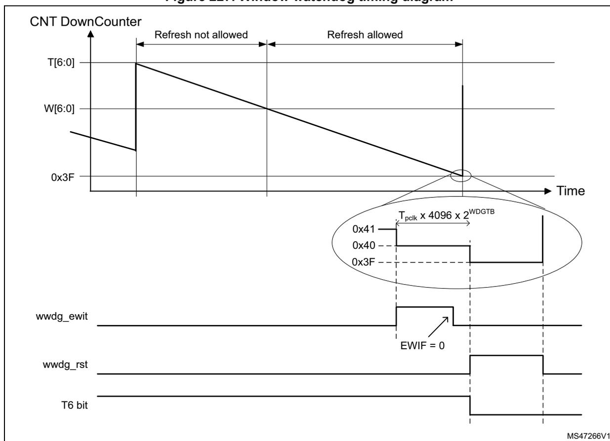
The diagram shows the behavior of the WWDG counter (CNT DownCounter) over time. The counter starts at value T[6:0] and decrements. A horizontal line represents the window value W[6:0]. The period before the counter reaches W[6:0] is labeled 'Refresh not allowed'. The period between W[6:0] and 0x3F is labeled 'Refresh allowed'. A zoomed-in circle shows the transition from 0x41 to 0x40 and finally to 0x3F, with a time interval labeled \( T_{pclk} \times 4096 \times 2^{WDGTB} \) . Below the counter graph, three digital signals are shown: wwdg_ewit (which pulses high when EWIF = 0), wwdg_rst (which pulses high when the counter reaches 0x3F), and the T6 bit (which drops to 0 when the reset occurs). The diagram is identified by the code MS47266V1.
The formula to calculate the timeout value is given by:
where:
\( t_{WWDG} \) : WWDG timeout
\( t_{PCLK} \) : APB clock period measured in ms
4096: value corresponding to internal divider
As an example, let's assume APB frequency is equal to 48 MHz, WDGTB[1:0] is set to 3 and T[5:0] is set to 63:
Refer to the datasheet for the minimum and maximum values of the \( t_{\text{WWDG}} \) .
22.3.5 Debug mode
When the device enters debug mode (processor halted), the WWDG counter either continues to work normally or stops, depending on the configuration bit in DBG module. For more details refer to Section 29: Debug support (DBG) .
22.4 WWDG interrupts
The early wakeup interrupt (EWI) can be used if specific safety operations or data logging must be performed before the actual reset is generated. The EWI interrupt is enabled by setting the EWI bit in the WWDG_CFR register. When the down-counter reaches the value 0x40, an EWI interrupt is generated and the corresponding interrupt service routine (ISR) can be used to trigger specific actions (such as communications or data logging), before resetting the device.
In some applications, the EWI interrupt can be used to manage a software system check and/or system recovery/graceful degradation, without generating a WWDG reset. In this case, the corresponding interrupt service routine (ISR) has to reload the WWDG counter to avoid the WWDG reset, then trigger the required actions.
The EWI interrupt is cleared by writing '0' to the EWIF bit in the WWDG_SR register.
Note: When the EWI interrupt cannot be served, e.g. due to a system lock in a higher priority task, the WWDG reset is eventually generated.
22.5 WWDG registers
Refer to Section 1.2 on page 39 for a list of abbreviations used in register descriptions.
The peripheral registers can be accessed by halfwords (16-bit) or words (32-bit).
22.5.1 WWDG control register (WWDG_CR)
Address offset: 0x000
Reset value: 0x0000 007F
| 31 | 30 | 29 | 28 | 27 | 26 | 25 | 24 | 23 | 22 | 21 | 20 | 19 | 18 | 17 | 16 |
|---|---|---|---|---|---|---|---|---|---|---|---|---|---|---|---|
| Res. | Res. | Res. | Res. | Res. | Res. | Res. | Res. | Res. | Res. | Res. | Res. | Res. | Res. | Res. | Res. |
| 15 | 14 | 13 | 12 | 11 | 10 | 9 | 8 | 7 | 6 | 5 | 4 | 3 | 2 | 1 | 0 |
| Res. | Res. | Res. | Res. | Res. | Res. | Res. | Res. | WDGA | T[6:0] | ||||||
| rs | rw | rw | rw | rw | rw | rw | rw | ||||||||
Bits 31:8 Reserved, must be kept at reset value.
Bit 7 WDGA : Activation bit
This bit is set by software and only cleared by hardware after a reset. When WDGA = 1, the watchdog can generate a reset.
0: Watchdog disabled
1: Watchdog enabled
Bits 6:0 T[6:0] : 7-bit counter (MSB to LSB)
These bits contain the value of the watchdog counter, decremented every \( (4096 \times 2^{\text{WDGTB}[1:0]}) \) PCLK cycles. A reset is produced when it is decremented from 0x40 to 0x3F (T6 becomes cleared).
22.5.2 WWDG configuration register (WWDG_CFR)
Address offset: 0x004
Reset value: 0x0000 007F
| 31 | 30 | 29 | 28 | 27 | 26 | 25 | 24 | 23 | 22 | 21 | 20 | 19 | 18 | 17 | 16 |
|---|---|---|---|---|---|---|---|---|---|---|---|---|---|---|---|
| Res. | Res. | Res. | Res. | Res. | Res. | Res. | Res. | Res. | Res. | Res. | Res. | Res. | Res. | Res. | Res. |
| 15 | 14 | 13 | 12 | 11 | 10 | 9 | 8 | 7 | 6 | 5 | 4 | 3 | 2 | 1 | 0 |
| Res. | Res. | WDGTB[2:0] | Res. | EWI | Res. | Res. | W[6:0] | ||||||||
| rw | rw | rw | rs | rw | rw | rw | rw | rw | rw | rw | |||||
Bits 31:10 Reserved, must be kept at reset value.
Bits 13:11 WDGTB[2:0] : Timer base
The timebase of the prescaler can be modified as follows:
000: CK Counter Clock (PCLK div 4096) div 1
001: CK Counter Clock (PCLK div 4096) div 2
010: CK Counter Clock (PCLK div 4096) div 4
011: CK Counter Clock (PCLK div 4096) div 8
100: CK Counter Clock (PCLK div 4096) div 16
101: CK Counter Clock (PCLK div 4096) div 32
110: CK Counter Clock (PCLK div 4096) div 64
111: CK Counter Clock (PCLK div 4096) div 128
Bit 9 EWI : Early wakeup interrupt
When set, an interrupt occurs whenever the counter reaches the value 0x40. This interrupt is only cleared by hardware after a reset.
Bits 6:0 W[6:0] : 7-bit window value
These bits contain the window value to be compared with the down-counter.
22.5.3 WWDG status register (WWDG_SR)
Address offset: 0x008
Reset value: 0x0000 0000
| 31 | 30 | 29 | 28 | 27 | 26 | 25 | 24 | 23 | 22 | 21 | 20 | 19 | 18 | 17 | 16 |
|---|---|---|---|---|---|---|---|---|---|---|---|---|---|---|---|
| Res. | Res. | Res. | Res. | Res. | Res. | Res. | Res. | Res. | Res. | Res. | Res. | Res. | Res. | Res. | Res. |
| 15 | 14 | 13 | 12 | 11 | 10 | 9 | 8 | 7 | 6 | 5 | 4 | 3 | 2 | 1 | 0 |
| Res. | Res. | Res. | Res. | Res. | Res. | Res. | Res. | Res. | Res. | Res. | Res. | Res. | Res. | Res. | EWIF |
| rc_w0 |
Bits 31:1 Reserved, must be kept at reset value.
Bit 0 EWIF : Early wakeup interrupt flag
This bit is set by hardware when the counter has reached the value 0x40. It must be cleared by software by writing '0'. Writing '1' has no effect. This bit is also set if the interrupt is not enabled.
22.5.4 WWDG register map
The following table gives the WWDG register map and reset values.
Table 86. WWDG register map and reset values
| Offset | Register | 31 | 30 | 29 | 28 | 27 | 26 | 25 | 24 | 23 | 22 | 21 | 20 | 19 | 18 | 17 | 16 | 15 | 14 | 13 | 12 | 11 | 10 | 9 | 8 | 7 | 6 | 5 | 4 | 3 | 2 | 1 | 0 |
|---|---|---|---|---|---|---|---|---|---|---|---|---|---|---|---|---|---|---|---|---|---|---|---|---|---|---|---|---|---|---|---|---|---|
| 0x000 | WWDG_CR | Res. | Res. | Res. | Res. | Res. | Res. | Res. | Res. | Res. | Res. | Res. | Res. | Res. | Res. | Res. | Res. | Res. | Res. | Res. | Res. | Res. | Res. | Res. | Res. | WDGA | T[6:0] | ||||||
| Reset value | 0 | 1 | 1 | 1 | 1 | 1 | 1 | 1 | |||||||||||||||||||||||||
| 0x004 | WWDG_CFR | Res. | Res. | Res. | Res. | Res. | Res. | Res. | Res. | Res. | Res. | Res. | Res. | Res. | Res. | Res. | Res. | Res. | Res. | WDGTB [2:0] | Res. | Res. | Res. | EWI | Res. | Res. | W[6:0] | ||||||
| Reset value | 0 | 0 | 0 | 0 | 1 | 1 | 1 | 1 | 1 | 1 | |||||||||||||||||||||||
| 0x008 | WWDG_SR | Res. | Res. | Res. | Res. | Res. | Res. | Res. | Res. | Res. | Res. | Res. | Res. | Res. | Res. | Res. | Res. | Res. | Res. | Res. | Res. | Res. | Res. | Res. | Res. | Res. | Res. | Res. | Res. | Res. | Res. | Res. | EWIF |
| Reset value | 0 | ||||||||||||||||||||||||||||||||
Refer to Section 2.2 on page 44 for the register boundary addresses.