5. Reset and clock control (RCC)
5.1 Reset
There are three types of reset, defined as system reset, power reset and RTC domain reset.
5.1.1 Power reset
A power reset is generated when one of the following events occurs:
- • power-on reset (POR)
- • exit from Standby mode
Power reset set all registers to their reset values except the registers of the RTC domain.
When exiting Standby mode, all registers in the \( V_{CORE} \) domain are set to their reset value. Registers outside the \( V_{CORE} \) domain (RTC, WKUP, IWDG, and Standby mode control) is not impacted.
5.1.2 System reset
System reset sets all registers to their reset values except the reset flags in the clock control/status register (RCC_CSR) and the registers in the RTC domain.
System reset is generated when one of the following events occurs:
- • low level on the NRST pin (external reset)
- • window watchdog event (WWDG reset)
- • independent watchdog event (IWDG reset)
- • software reset (SW reset) (see Software reset )
- • low-power mode security reset (see Low-power mode security reset )
- • option byte loader reset (see Option byte loader reset )
- • power-on reset
The reset source can be identified by checking the reset flags in the RCC_CSR register (see Section 5.4.23: Control/status register (RCC_CSR) ).
NRST pin (external reset):
Valid reset signal on the pin is propagated to the internal logic, and each internal reset source is led to a pulse generator the output of which drives this pin. The pulse generator guarantees a minimum reset pulse duration of 20 µs for each internal reset source to be output on the NRST pin.
Figure 7. Simplified diagram of the reset circuit
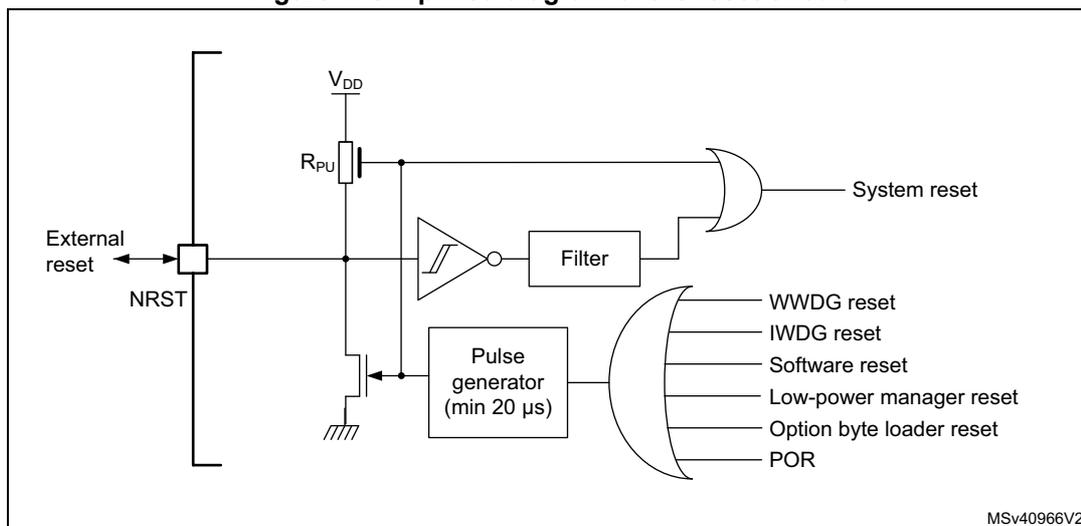
The diagram illustrates the internal reset circuitry. An external reset pin is labeled 'NRST'. A pull-up resistor, labeled \( R_{PU} \) , is connected between the \( V_{DD} \) supply and the NRST pin. The NRST pin is connected to an inverter. The output of this inverter is connected to a 'Filter' block. The output of the filter is connected to one input of an OR gate, which produces the 'System reset' signal. The NRST pin is also connected to a 'Pulse generator (min 20 \( \mu s \) )' block. The output of the pulse generator is connected to another input of the OR gate. The OR gate also receives six other reset signals as inputs: 'WWDG reset', 'IWDG reset', 'Software reset', 'Low-power manager reset', 'Option byte loader reset', and 'POR'. The diagram is labeled with the code 'MSV40966V2' in the bottom right corner.
Caution: Upon power reset, the NRST pin is configured as Reset input/output and driven low by the system until it is reconfigured to the expected mode when the option bytes are loaded, in the fourth clock cycle after the end of trstempo.
Software reset
The SYSRESETREQ bit in Cortex ® -M0+ Application interrupt and reset control register must be set to force a software reset on the device (refer to the programming manual PM0223).
Low-power mode security reset
To prevent that critical applications mistakenly enter a low-power mode, two low-power mode security resets are available. If enabled in option bytes, the resets are generated in the following conditions:
- • Entering Standby mode
This type of reset is enabled by resetting nRST_STDBY bit in user option bytes. In this case, whenever a Standby mode entry sequence is successfully executed, the device is reset instead of entering Standby mode.
- • Entering Stop mode
This type of reset is enabled by resetting nRST_STOP bit in user option bytes. In this case, whenever a Stop mode entry sequence is successfully executed, the device is reset instead of entering Stop mode.
For further information on the user option bytes, refer to Section 3.4.1: FLASH option byte description .
Option byte loader reset
The option byte loader reset is generated when the OBL_LAUNCH bit (bit 27) is set in the FLASH_CR register. This bit is used to launch the option byte loading by software.
5.1.3 RTC domain reset
The RTC domain has two specific resets.
A RTC domain reset is generated when one of the following events occurs:
- • Software reset , triggered by setting the BDRST bit in the RTC domain control register (RCC_BDCR) .
- • V DD or V BAT power on , if both supplies have previously been powered off.
A RTC domain reset only affects the LSE oscillator, the RTC, the backup registers and the RCC RTC domain control register.
5.2 Clocks
The device provides the following clock sources producing primary clocks:
- • HSI16 RC - a high-speed fully-integrated RC oscillator producing HSI16 clock (about 16 MHz)
- • HSE OSC - a high-speed oscillator with external crystal/ceramic resonator or external clock source, producing HSE clock (4 to 48 MHz)
- • LSI RC - a low-speed fully-integrated RC oscillator producing LSI clock (about 32 kHz)
- • LSE OSC - a low-speed oscillator with external crystal/ceramic resonator or external clock source, producing LSE clock (accurate 32.768 kHz or external clock up to 1 MHz)
- • I2S_CKIN - pin for direct clock input for I2S1 peripheral
Each oscillator can be switched on or off independently when it is not used, to optimize power consumption. Check sub-sections of this section for more functional details. For electrical characteristics of the internal and external clock sources, refer to the device datasheet.
The device produces secondary clocks by dividing or/and multiplying the primary clocks:
- • HSISYS - a clock derived from HSI16 through division by a factor programmable from 1 to 128
- • PLLPCLK, PLLQCLK and PLLRCLK - clocks output from the PLL block
- • SYSCLK - a clock obtained through selecting one of LSE, LSI, HSE, PLLRCLK, and HSISYS clocks
- • HCLK - a clock derived from SYSCLK through division by a factor programmable from 1 to 512
- • HCLK8 - a clock derived from HCLK through division by eight
- • PCLK - a clock derived from HCLK through division by a factor programmable from 1 to 16
- • TIMPCLK - a clock derived from PCLK, running at PCLK frequency if the APB prescaler division factor is set to 1, or at twice the PCLK frequency otherwise
More secondary clocks are generated by fixed division of HSE, HSI16 and HCLK clocks.
The HSISYS is used as system clock source after startup from reset, with the division by 1 (producing HSI16 frequency).
The HCLK clock and PCLK clock are used for clocking the AHB and the APB domains, respectively. Their maximum allowed frequency is 64 MHz.
The peripherals are clocked with the clocks from the bus they are attached to (HCLK for AHB, PCLK for APB) except:
- •
TIMx
, with these clock sources to select from:
- – TIMPCLK (selectable for all timers) running at PCLK frequency if the APB prescaler division factor is set to 1, or at twice the PCLK frequency otherwise
- •
ADC
, with these clock sources to select from:
- – SYSCLK (system clock)
- – HSI16
- – PLLPCLK
- •
USARTx
, with these clock sources to select from:
- – SYSCLK (system clock)
- – HSI16
- – LSE
- – PCLK (APB clock)
The wakeup from Stop mode is supported only when the clock is HSI16 or LSE.
- •
I2Cx
, with these clock sources to select from:
- – SYSCLK (system clock)
- – HSI16
- – PCLK (APB clock)
The wakeup from Stop mode is supported only when the clock is HSI16.
- •
I2Sx
, with these clock sources to select from:
- – SYSCLK (system clock)
- – HSI16
- – PLLPCLK
- – I2S_CKIN pin
- •
RTC
, with these clock sources to select from:
- – LSE
- – LSI
- – HSE clock divided by 32
The functionality in Stop mode (including wakeup) is supported only when the clock is LSI or LSE.
- • IWDG , always clocked with LSI clock.
- •
USB
, with these clocks to select from:
- – HSE
- – PLLQCLK
- •
SysTick
(Cortex
®
core system timer), with these clock sources to select from:
- – HCLK (AHB clock)
- – HCLK clock divided by 8
The selection is done through SysTick control and status register.
HCLK is used as Cortex ® -M0+ free-running clock (FCLK). For more details, refer to the programming manual PM0223.
Figure 8. Clock tree
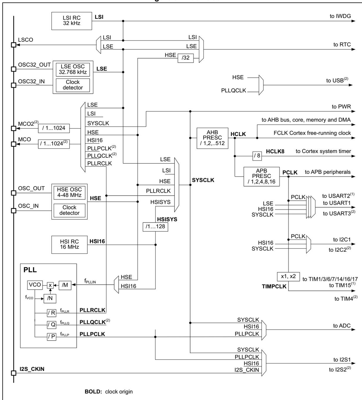
The diagram illustrates the internal clock architecture of an STM32 microcontroller. It shows the following components and connections:
- LSI RC 32 kHz: Provides the LSI clock signal to the IWDG and RTC.
- LSE OSC 32.768 kHz: Connected to OSC32_IN and OSC32_OUT pins. It provides the LSE clock to the RTC and can be selected as a system clock source.
- HSE OSC 4-48 MHz: Connected to OSC_IN and OSC_OUT pins. It provides the HSE clock to the PLL and can be selected as a system clock source.
- HSI RC 16 MHz: Internal high-speed oscillator providing the HSI16 clock to the PLL and HSISYS.
- PLL: A phase-locked loop that takes HSE or HSI16 as input (f PLLIN ). It contains a VCO with feedback dividers (/N, /M) and output dividers (/R, /Q, /P) to generate PLLRCLK, PLLQCLK (2) , and PLLPCLK.
- System Clock (SYSCLK): The main system clock, selectable from LSI, LSE, HSE, HSI16, PLLRCLK, PLLQCLK (2) , or PLLPCLK. It is distributed to the AHB bus, core, memory, and DMA.
- AHB Prescaler: Divides SYSCLK by 1, 2, ..., 512 to produce HCLK (FCLK Cortex free-running clock).
- APB Prescaler: Divides HCLK by 1, 2, 4, 8, 16 to produce PCLK for APB peripherals.
- Other Clock Outputs:
- LSCO: Output of the LSI or LSE clock.
- OSC32_OUT: Output of the LSE OSC.
- OSC_OUT: Output of the HSE OSC.
- MCO (2) : Microcontroller Clock Output, selectable from various clock sources with a divider of /1...1024.
- Peripheral Clocks:
- HCLK8: HCLK divided by 8, used for the Cortex system timer.
- PCLK: Used for USART2 (1) , USART1, USART3 (2) , I2C1, and I2C2 (2) .
- TIMPCLK: Generated from TIMPCLK source (x1, x2) and used for TIM1/3/6/7/14/16/17 to TIM15 (1) and TIM4 (2) .
- ADC Clock: Derived from SYSCLK, HSI16, or PLLPCLK.
- I2S Clock: Derived from SYSCLK, PLLPCLK, HSI16, or I2S_CKIN, used for I2S1 and I2S2 (2) .
BOLD: clock origin
1. Only applies to STM32G070xx and to STM32G0B0xx.
2. Only applies to STM32G0B0xx.
5.2.1 HSE clock
The high speed external clock signal (HSE) can be generated from two possible clock sources:
- • HSE external crystal/ceramic resonator
- • HSE user external clock
The resonator and the load capacitors have to be placed as close as possible to the oscillator pins in order to minimize output distortion and startup stabilization time. The loading capacitance values must be adjusted according to the selected oscillator.
Figure 9. HSE/ LSE clock sources
| Clock source | Hardware configuration |
|---|---|
| External clock | 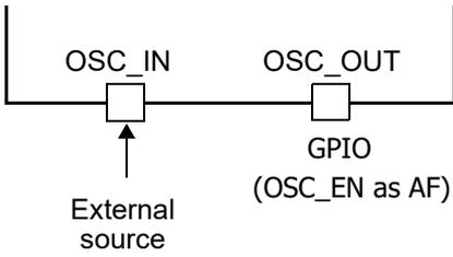 |
| Crystal/Ceramic resonators | 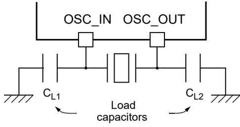 |
External crystal/ceramic resonator (HSE crystal)
The 4 to 48 MHz external oscillator has the advantage of producing a very accurate rate on the main clock.
The associated hardware configuration is shown in Figure 9 . Refer to the electrical characteristics section of the datasheet for more details.
The HSERDY flag in the Clock control register (RCC_CR) indicates if the HSE oscillator is stable or not. At startup, the clock is not released until this bit is set by hardware. An interrupt can be generated if enabled in the Clock interrupt enable register (RCC_CIER) .
The HSE Crystal can be switched on and off using the HSEON bit in the Clock control register (RCC_CR) .
External source (HSE bypass)
In this mode, an external clock source must be provided. It can have a frequency of up to 48 MHz. This mode is selected by setting the HSEBYP and HSEON bits in the Clock control register (RCC_CR) . The external clock signal (square, sinus or triangle) with ~40-60 % duty cycle depending on the frequency (refer to the datasheet ) must drive the OSC_IN pin, on devices where OSC_IN and OSC_OUT pins are available (see Figure 9 ). The OSC_OUT pin can be used as a GPIO.
The OSC_OUT pin can be used as a GPIO or it can be configured as OSC_EN alternate function, to provide an enable signal to external clock synthesizer. It allows stopping the external clock source when the device enters low power modes.
Note: For details on pin availability, refer to the pinout section in the corresponding device datasheet.
To minimize the consumption, it is recommended to use the square signal.
5.2.2 HSI16 clock
The HSI16 clock signal is generated from an internal 16 MHz RC oscillator.
The HSI16 RC oscillator has the advantage of providing a clock source at low cost (no external components). It also has a faster startup time than the HSE crystal oscillator. However, even after calibration, it is less accurate than an oscillator using a frequency reference such as quartz crystal or ceramic resonator.
The HSISYS clock derived from HSI16 can be selected as system clock after wakeup from Stop modes (Stop 0 or Stop 1). Refer to Section 5.3: Low-power modes . It can also be used as a backup clock source (auxiliary clock) if the HSE crystal oscillator fails. Refer to Section 5.2.8: Clock security system (CSS) .
Calibration
RC oscillator frequencies can vary from one chip to another due to manufacturing process variations.
After reset, the factory calibration value is loaded in the HSICAL[7:0] bits in the Internal clock source calibration register (RCC_ICSCR) .
Voltage or temperature variations in the application may affect the HSI16 frequency of the RC oscillator. It can be trimmed using the HSITRIM[6:0] bits in the Internal clock source calibration register (RCC_ICSCR) .
For more details on how to measure the HSI16 frequency variation, refer to Section 5.2.15: Internal/external clock measurement with TIM14/TIM16/TIM17 .
The HSIRDY flag in the Clock control register (RCC_CR) indicates if the HSI16 RC is stable or not. At startup, the HSI16 RC output clock is not released until this bit is set by hardware.
The HSI16 RC can be switched on and off using the HSION bit in the Clock control register (RCC_CR) .
The HSI16 signal can also be used as a backup source (auxiliary clock) if the HSE crystal oscillator fails. Refer to Section 5.2.8: Clock security system (CSS) on page 129 .
5.2.3 PLL
The internal PLL multiplies the frequency of HSI16- or HSE-based clock fetched on its input, to produce three independent clock outputs. The allowed input frequency range is from 2.66 to 16 MHz. The dedicated divider PLLM with division factor programmable from one to eight allows setting a frequency within the valid PLL input range. Refer to Figure 8: Clock tree and PLL configuration register (RCC_PLLCFGR) .
The PLL configuration (selection of the input clock and multiplication factor) must be done before enabling the PLL. Once the PLL is enabled, these parameters cannot be changed.
To modify the PLL configuration, proceed as follows:
- 1. Disable the PLL by setting PLLON to 0 in Clock control register (RCC_CR) .
- 2. Wait until PLLRDY is cleared. The PLL is now fully stopped.
- 3. Change the desired parameter.
- 4. Enable the PLL again by setting PLLON to 1.
- 5. Enable the desired PLL outputs by configuring PLLPEN, PLLQEN, and PLLREN in PLL configuration register (RCC_PLLCFGR) .
An interrupt can be generated when the PLL is ready, if enabled in the Clock interrupt enable register (RCC_CIER) .
The enable bit of each PLL output clock (PLLPEN, PLLQEN, and PLLREN) can be modified at any time without stopping the PLL. PLLREN cannot be cleared if PLLRCLK is used as system clock.
5.2.4 LSE clock
The LSE crystal is a 32.768 kHz crystal or ceramic resonator. It has the advantage of providing a low-power but highly accurate clock source to the real-time clock peripheral (RTC) for clock/calendar or other timing functions.
The LSE crystal is switched on and off using the LSEON bit in RTC domain control register (RCC_BDCR) . The crystal oscillator driving strength can be changed at runtime using the LSEDRV[1:0] bits in the RTC domain control register (RCC_BDCR) to obtain the best compromise between robustness and short start-up time on one side and low-power-consumption on the other side. The LSE drive can be decreased to the lower drive capability (LSEDRV=00) when the LSE is ON. However, once LSEDRV is selected, the drive capability can not be increased if LSEON=1.
The LSERDY flag in the RTC domain control register (RCC_BDCR) indicates whether the LSE crystal is stable or not. At startup, the LSE crystal output clock signal is not released until this bit is set by hardware. An interrupt can be generated if enabled in the Clock interrupt enable register (RCC_CIER) .
External source (LSE bypass)
In this mode, an external clock source must be provided. It can have a frequency of up to 1 MHz. This mode is selected by setting the LSEBYP and LSEON bits in the AHB peripheral clock enable in Sleep/Stop mode register (RCC_AHBSENMR) . The external clock signal (square, sinus or triangle) with ~50 % duty cycle has to drive the OSC32_IN pin while the OSC32_OUT pin can be used as GPIO. See Figure 9 .
5.2.5 LSI clock
The LSI RC acts as a low-power clock source that can be kept running in Stop and Standby mode for the independent watchdog (IWDG) and RTC. The clock frequency is 32 kHz. For more details, refer to the electrical characteristics section of the datasheets.
The LSI RC can be switched on and off using the LSION bit in the Control/status register (RCC_CSR) .
The LSIRDY flag in the Control/status register (RCC_CSR) indicates if the LSI oscillator is stable or not. At startup, the clock is not released until this bit is set by hardware. An interrupt can be generated if enabled in the Clock interrupt enable register (RCC_CIER) .
5.2.6 System clock (SYSCLK) selection
One of the following clocks can be selected as system clock (SYSCLK):
- • LSI
- • LSE
- • HSISYS
- • HSE
- • PLLRCLK
The system clock maximum frequency is 64 MHz. Upon system reset, the HSISYS clock derived from HSI16 oscillator is selected as system clock. When a clock source is used directly or through the PLL as a system clock, it is not possible to stop it.
A switch from one clock source to another occurs only if the target clock source is ready (clock stable after startup delay or PLL locked). If a clock source which is not yet ready is selected, the switch occurs when the clock source becomes ready. Status bits in the Internal clock source calibration register (RCC_ICSCR) indicate which clock(s) is (are) ready and which clock is currently used as a system clock.
5.2.7 Clock source frequency versus voltage scaling
The following table gives the different clock source frequencies depending on the product voltage range.
Table 27. Clock source frequency
| Clock | Maximum clock frequency (MHz) | |
|---|---|---|
| Range 1 | Range 2 | |
| HSI16 | 16 | 16 |
| HSE | 48 | 16 |
| PLLPCLK | 122 (1) | 40 (2) |
Table 27. Clock source frequency (continued)
| Clock | Maximum clock frequency (MHz) | |
|---|---|---|
| Range 1 | Range 2 | |
| PLLQCLK | 128 (1) | 32 (2) |
| PLLRCLK | 64 (1) | 16 (2) |
1. Maximum VCO frequency is 344 MHz.
2. Maximum VCO frequency is 128 MHz.
5.2.8 Clock security system (CSS)
Clock security system can be activated by software. In this case, the clock detector is enabled after the HSE oscillator startup delay, and disabled when this oscillator is stopped.
If a failure is detected on the HSE clock:
- the HSE oscillator is automatically disabled
- a clock failure event is sent to the break input of TIM1, TIM15, TIM16 and TIM17 timers
- CSSI (clock security system interrupt) is generated
The CSSI is linked to the Cortex ® -M0+ NMI (non-maskable interrupt) exception vector. It makes the software aware of a HSE clock failure to allow it to perform rescue operations.
Note: If the CSS is enabled and the HSE clock fails, the CSSI occurs and an NMI is automatically generated. The NMI is executed infinitely unless the CSS interrupt pending bit is cleared. It is therefore necessary that the NMI ISR clears the CSSI by setting the CSSC bit in the Clock interrupt clear register (RCC_CICR).
If HSE is selected directly or indirectly (PLLRCLK selected for SYSCLK and HSE selected as PLL input) as system clock, and a failure of HSE clock is detected, the system clock switches automatically to HSISYS and the HSE oscillator is disabled. If the HSE clock (divided or not) is the clock entry of the PLL and PLLRCLK is used as system clock when the failure occurs, the PLL is disabled, too.
5.2.9 Clock security system for LSE clock (LSECSS)
A clock security system on LSE can be activated by setting the LSECSSON bit in RTC domain control register (RCC_BDCR) . This bit can be cleared only by a hardware reset or RTC software reset, or after LSE clock failure detection. LSECSSON must be written after LSE and LSI are enabled (LSEON and LSION enabled) and ready (LSERDY and LSIRDY flags set by hardware), and after selecting the RTC clock by RTCSEL.
The LSECSS works in all modes except VBAT. It keeps working also under system reset (excluding power-on reset). If a failure is detected on the LSE oscillator, the LSE clock is no longer supplied to the RTC but its registers are not impacted.
Note: If the LSECSS is enabled and the LSE clock fails, the LSECSSI occurs and an NMI is automatically generated. The NMI is executed infinitely unless the LSECSS interrupt pending bit is cleared. It is therefore necessary that the NMI ISR clears the LSECSSI by setting the LSECSSC bit in the Clock interrupt clear register (RCC_CICR).
If LSE is used as system clock, and a failure of LSE clock is detected, the system clock switches automatically to LSI. In low-power modes, an LSE clock failure generates a wakeup. The interrupt flag must then be cleared within the RCC registers.
The software must then disable the LSECSSON bit, stop the defective 32 kHz oscillator (by clearing LSEON), and change the RTC clock source (no clock, LSI or HSE, with RTCSEL), or take any appropriate action to secure the application.
The frequency of the LSE oscillator must exceed 30 kHz to avoid false positive detections.
5.2.10 ADC clock
The ADC clock is derived from the system clock, or from the PLLPCLK output. It can reach 122 MHz and can be divided by the following prescalers values:
1,2,4,6,8,10,12,16,32,64,128 or 256 by configuring the ADC1_CCR register. It is asynchronous to the AHB clock. Alternatively, the ADC clock can be derived from the AHB clock of the ADC bus interface, divided by a programmable factor (1, 2 or 4). This programmable factor is configured using the CKMODE bitfields in the ADC1_CCR.
If the programmed factor is 1, the AHB prescaler must be set to 1.
5.2.11 RTC clock
The RTCCLK clock source can be either the HSE/32, LSE or LSI clock. It is selected by programming the RTCSEL[1:0] bits in the RTC domain control register (RCC_BDCR) . This selection cannot be modified without resetting the RTC domain. The system must always be configured so as to get a PCLK frequency greater then or equal to the RTCCLK frequency for a proper operation of the RTC.
The LSE clock is in the RTC domain, whereas the HSE and LSI clocks are not. Consequently:
- • If LSE is selected as RTC clock:
- – The RTC continues to work even if the \( V_{DD} \) supply is switched off, provided the \( V_{BAT} \) supply is maintained.
- • If LSI is selected as the RTC clock:
- – The RTC state is not guaranteed if the \( V_{DD} \) supply is powered off.
- • If the HSE clock divided by a prescaler is used as the RTC clock:
- – The RTC state is not guaranteed if the \( V_{DD} \) supply is powered off or if the internal voltage regulator is powered off (removing power from the \( V_{CORE} \) domain).
When the RTC clock is LSE or LSI, the RTC remains clocked and functional under system reset.
5.2.12 Timer clock
The timer clock TIMPCLK is derived from PCLK (used for APB) as follows:
- 1. If the APB prescaler is set to 1, TIMPCLK frequency is equal to PCLK frequency.
- 2. Otherwise, the TIMPCLK frequency is set to twice the PCLK frequency.
5.2.13 Watchdog clock
If the Independent watchdog (IWDG) is started by either hardware option or software access, the LSI oscillator is forced ON and cannot be disabled. After the LSI oscillator temporization, the clock is provided to the IWDG.
5.2.14 Clock-out capability
MCO and MCO2
The MCO and MCO2 pins output, independently of each other, the clock selected from:
- • LSI
- • LSE
- • SYSCLK
- • HSI16
- • HSE
- • PLLPCLK
- • PLLQCLK
- • PLLRCLK
- • RTCCLK
- • RTC WAKEUP
The multiplexers for MCO and MCO2, respectively, are controlled by the MCOSEL[3:0] and MCO2SEL[3:0] bitfields of the Clock configuration register (RCC_CFGR) . Their outputs are further divided by a factor set through the MCOPRE[2:0] and MCO2PRE[2:0] bitfields of the Clock configuration register (RCC_CFGR) .
Note: The MCO2 output and the associated MCO2SEL[3:0] and MCO2PRE[2:0] bitfields are only available on the STM32G0B0xx devices. On the other devices, the divider ratio is limited to 128 and the clock sources do not include PLLPCLK, PLLQCLK, RTCCLK, and RTC WAKEUP.
LSCO
The LSCO pin allows outputting one of low-speed clocks:
- • LSI
- • LSE
The selection is controlled by the LSCOSEL bit and enabled with the LSCOEN bit of the RTC domain control register (RCC_BDCR) . The configuration registers of the corresponding GPIO port must be programmed in alternate function mode.
This function remains available in Stop 0, Stop 1 and Standby modes.
5.2.15 Internal/external clock measurement with TIM14/TIM16/TIM17
It is possible to indirectly measure the frequency of all on-board clock sources with the TIM14, TIM16 and TIM17 channel 1 input capture, as represented in Figure 10 , Figure 11 and Figure 12 .
TIM14
By setting the TI1SEL[3:0] field of the TIM14_TISEL register, the clock selected for the input capture channel1 of TIM14 can be one of:
- • GPIO (refer to the alternate function mapping in the device datasheets)
- • RTC clock (RTCCLK)
- • HSE clock divided by 32
- • MCO (MCU clock output)
The last option is controlled by the MCOSEL[3:0] field of the clock configuration register (RCC_CFGR). All clock sources can be selected for the MCO pin.
Figure 10. Frequency measurement with TIM14 in capture mode
![Figure 10: Frequency measurement with TIM14 in capture mode. The diagram shows a multiplexer selecting between GPIO, RTCCLK, HSE (divided by 32), and MCO as input for the TI1 pin of TIM 14. The selection is controlled by the TI1SEL[3:0] register field. The output of the multiplexer is connected to the TI1 input of the TIM 14 block. The diagram is labeled MSV42174V1.](/RM0454-STM32G0x0/50a63fe40eaa16cb8745c689fe8f8264_img.jpg)
The diagram illustrates the internal connections for frequency measurement using TIM14. On the left, a 4-to-1 multiplexer is shown. Its inputs are labeled GPIO, RTCCLK, HSE (with a /32 divider), and MCO. The output of the multiplexer is connected to the TI1 input of a block labeled 'TIM 14'. Above the multiplexer, a label 'TI1SEL[3:0]' indicates the control signal for the selection. In the bottom right corner, the text 'MSV42174V1' is present.
TIM16
By setting the TI1SEL[3:0] field of the TIM16_TISEL register, the clock selected for the input capture channel1 of TIM16 can be one of:
- • GPIO (refer to the alternate function mapping in the device datasheets).
- • LSI clock
- • LSE clock
- • RTC wakeup interrupt signal
The last option requires to enable the RTC interrupt.
Figure 11. Frequency measurement with TIM16 in capture mode
![Figure 11: Frequency measurement with TIM16 in capture mode. The diagram shows a multiplexer selecting between GPIO, LSI, LSE, and RTC wakeup interrupt as input for the TI1 pin of TIM 16. The selection is controlled by the TI1SEL[3:0] register field. The output of the multiplexer is connected to the TI1 input of the TIM 16 block. The diagram is labeled MSV42175V1.](/RM0454-STM32G0x0/43ff52fe5a7c6990f4f0d5e0ca55d4b4_img.jpg)
The diagram shows the internal connections for frequency measurement using TIM16. A 4-to-1 multiplexer on the left has inputs for GPIO, LSI, LSE, and RTC wakeup interrupt. Its output is connected to the TI1 input of a block labeled 'TIM 16'. The multiplexer is controlled by the 'TI1SEL[3:0]' field. The text 'MSV42175V1' is located in the bottom right corner.
TIM17
By setting the TI1SEL[3:0] field of the TIM17_TISEL register, the clock selected for the input capture channel1 of TIM17 can be one of:
- • GPIO Refer to the alternate function mapping in the device datasheets.
- • HSE divided by 32
- • MCO (MCU clock output)
The last option is controlled by the MCOSEL[3:0] field of the clock configuration register (RCC_CFGR). All clock sources can be selected for the MCO pin.
Figure 12. Frequency measurement with TIM17 in capture mode
![Diagram illustrating frequency measurement with TIM17 in capture mode. A TIM 17 block has a TI1 input connected to a multiplexer. The multiplexer selects between three sources: GPIO, HSE (divided by 32), and MCO. The selection is controlled by the TI1SEL[3:0] register. The diagram is labeled MSv42176V1.](/RM0454-STM32G0x0/db7a693cf26f527ac6c0d4d41da20858_img.jpg)
Calibration of the HSI16 oscillator
For TIM14, TIM15 and TIM17, the primary purpose of connecting the LSE to the channel 1 input capture is to precisely measure HSISYS (derived from HSI16) selected as system clock. Counting HSISYS clock pulses between consecutive edges of the LSE clock (the time reference) allows measuring the HSISYS (and HSI16) clock period. Such measurement can determine the HSI16 oscillator frequency with nearly the same accuracy as the accuracy of the 32.768 kHz quartz crystal used with the LSE oscillator (typically a few tens of ppm). The HSI16 oscillator can then be trimmed to compensate for deviations from target frequency, due to manufacturing, process, temperature and/or voltage variation.
The HSI16 oscillator has dedicated user-accessible calibration bits for this purpose.
The basic concept consists in providing a relative measurement (for example, the HSISYS/LSE ratio): the measurement accuracy is therefore closely related to the ratio between the two clock sources. Increasing the ratio allows improving the measurement accuracy.
Generated by the HSE oscillator, the HSE clock (divided by 32) used as time reference is the second best method for reaching a good HSI16 frequency measurement accuracy. It is recommended in absence of the LSE clock.
In order to further improve the precision of the HSI16 oscillator calibration, it is advised to employ one or a combination of the following measures to increase the frequency measurement accuracy:
- • set the HSISYS divider to 1 for HSISYS frequency to be equal to HSI16 frequency
- • average the results of multiple consecutive measurements
- • use the input capture prescaler of the timer (one capture every up to eight periods)
- • use LSE clock for the RTC and the RTC wakeup interrupt signal as time reference
The last point significantly increases the reference period for HSI16 clock pulse counting, which improves the accuracy of a single measurement. For operation, the RTC wakeup interrupt must be enabled.
Calibration of the LSI oscillator
The calibration of the LSI oscillator uses the same principle as that for calibrating the HSI16 oscillator. TIM16 channel1 input capture must be used for LSI clock, and HSE selected as system clock source. The number of HSE clock pulses between consecutive edges of the LSI signal, counted by TIM16, is then representative of the LSI clock period.
5.2.16 Peripheral clock enable registers
Each peripheral clock can be enabled by the corresponding enable bit of the RCC_AHBENR or RCC_APBENRx registers.
When the peripheral clock is not active, the peripheral registers read or write accesses are not supported.
Caution: The enable bit has a synchronization mechanism to create a glitch-free clock for the peripheral. After the enable bit is set, there is a 2-clock-cycle delay before the clock be active, which the software must take into account.
5.3 Low-power modes
- • AHB and APB peripheral clocks, including DMA clock, can be disabled by software.
- • Sleep and Low Power Sleep modes stops the CPU clock. The memory interface clocks (Flash memory and SRAM interfaces) can be stopped by software during sleep mode. The AHB to APB bridge clocks are disabled by hardware during Sleep mode when all the clocks of the peripherals connected to them are disabled.
- • Stop modes (Stop 0 and Stop 1) stop all the clocks in the \( V_{CORE} \) domain and disable the PLL as well as the HSI16 and HSE oscillators.
The USART1, USART2, USART3, I2C1, and I2C2 peripherals can enable the HSI16 oscillator even when the MCU is in Stop mode (if HSI16 is selected as clock source for one of those peripherals).
The USART1, USART2, and USART3 peripherals can also operate with the clock from the LSE oscillator when the system is in Stop mode, if LSE is selected as clock source for that peripheral and the LSE oscillator is enabled (LSEON set). In that case, the LSE oscillator remains active when the device enters Stop mode (these peripherals do not have the capability to turn on the LSE oscillator).
- • Standby mode stops all clocks in the \( V_{CORE} \) domain and disable the PLL, as well as the HSI16 and HSE oscillators.
The CPU deepsleep mode can be overridden for debugging, by setting the DBG_STOP or DBG_STANDBY bits in the DBGMCU_CR register.
When leaving the Stop 0 or Stop 1 modes, HSISYS becomes automatically the system clock.
When leaving the Standby mode, HSISYS (with frequency equal to HSI16) becomes automatically the system clock. At wakeup from Standby mode, the user trim is lost.
If a Flash memory programming operation is ongoing, Stop and Standby entry is delayed until the Flash memory interface access is finished. If an access to the APB domain is ongoing, the Stop and Standby entry is delayed until the APB access is finished.
5.4 RCC registers
Unless otherwise specified, the RCC registers support word, half-word, and byte access, without any wait state.
5.4.1 Clock control register (RCC_CR)
Address offset: 0x00
Power-on reset value: 0x0000 0500
Other types of reset: same as power-on reset, except HSEBYP bit that keeps its previous value.
| 31 | 30 | 29 | 28 | 27 | 26 | 25 | 24 | 23 | 22 | 21 | 20 | 19 | 18 | 17 | 16 |
|---|---|---|---|---|---|---|---|---|---|---|---|---|---|---|---|
| Res. | Res. | Res. | Res. | Res. | Res. | PLL RDY | PLLON | Res. | Res. | Res. | Res. | CSS ON | HSE BYP | HSE RDY | HSE ON |
| r | rw | rs | rw | r | rw | ||||||||||
| 15 | 14 | 13 | 12 | 11 | 10 | 9 | 8 | 7 | 6 | 5 | 4 | 3 | 2 | 1 | 0 |
| Res. | Res. | HSIDIV[2:0] | HSI RDY | HSI KERON | HSION | Res. | Res. | Res. | Res. | Res. | Res. | Res. | Res. | ||
| rw | rw | rw | r | rw | rw | ||||||||||
Bits 31:26 Reserved, must be kept at reset value.
Bit 25 PLLRDY : PLL clock ready flag
Set by hardware to indicate that the PLL is locked.
0: PLL unlocked
1: PLL locked
Bit 24 PLLON : PLL enable
Set and cleared by software to enable the PLL.
Cleared by hardware when entering Stop or Standby mode. This bit cannot be reset if the PLL clock is used as the system clock.
0: PLL OFF
1: PLL ON
Bits 23:20 Reserved, must be kept at reset value.
Bit 19 CSSON : Clock security system enable
Set by software to enable the clock security system. When CSSON is set, the clock detector is enabled by hardware when the HSE oscillator is ready, and disabled by hardware if a HSE clock failure is detected. This bit is set only and is cleared by reset.
0: Clock security system OFF (clock detector OFF)
1: Clock security system ON (Clock detector ON if the HSE oscillator is stable, OFF if not).
Bit 18 HSEBYP : HSE crystal oscillator bypass
Set and cleared by software to bypass the oscillator with an external clock. The external clock must be enabled with the HSEON bit set, to be used by the device. The HSEBYP bit can be written only if the HSE oscillator is disabled.
0: HSE crystal oscillator not bypassed
1: HSE crystal oscillator bypassed with external clock
Bit 17 HSERDY : HSE clock ready flag
Set by hardware to indicate that the HSE oscillator is stable.
0: HSE oscillator not ready
1: HSE oscillator ready
Note: Once the HSEON bit is cleared, HSERDY goes low after 6 HSE clock cycles.
Bit 16 HSEON : HSE clock enable
Set and cleared by software.
Cleared by hardware to stop the HSE oscillator when entering Stop or Standby mode. This bit cannot be reset if the HSE oscillator is used directly or indirectly as the system clock.
0: HSE oscillator OFF
1: HSE oscillator ON
Bits 15:14 Reserved, must be kept at reset value.
Bits 13:11 HSIDIV[2:0] : HSI16 clock division factor
This bitfield controlled by software sets division factor of the HSI16 clock divider to produce HSISYS clock:
000: 1
001: 2
010: 4
011: 8
100: 16
101: 32
110: 64
111: 128
Bit 10 HSIRDY : HSI16 clock ready flag
Set by hardware to indicate that HSI16 oscillator is stable. This bit is set only when HSI16 is enabled by software by setting HSION.
0: HSI16 oscillator not ready
1: HSI16 oscillator ready
Note: Once the HSION bit is cleared, HSIRDY goes low after 6 HSI16 clock cycles.
Bit 9 HSIKERON : HSI16 always enable for peripheral kernels.
Set and cleared by software to force HSI16 ON even in Stop modes. The HSI16 can only feed USART1, USART2, and I2C1 peripherals configured with HSI16 as kernel clock.
Keeping the HSI16 ON in Stop mode allows avoiding to slow down the communication speed because of the HSI16 startup time. This bit has no effect on HSION value.
0: No effect on HSI16 oscillator.
1: HSI16 oscillator is forced ON even in Stop mode.
Bit 8 HSION : HSI16 clock enable
Set and cleared by software.
Cleared by hardware to stop the HSI16 oscillator when entering Stop or Standby mode.
Forced by hardware to keep the HSI16 oscillator ON when it is used directly or indirectly as system clock (also when leaving Stop or Standby modes, or in case of failure of the HSE oscillator used for system clock).
0: HSI16 oscillator OFF
1: HSI16 oscillator ON
Bits 7:0 Reserved, must be kept at reset value.
5.4.2 Internal clock source calibration register (RCC_ICSCR)
Address offset: 0x04
Reset value: 0x0000 40XX, where X is factory-programmed.
| 31 | 30 | 29 | 28 | 27 | 26 | 25 | 24 | 23 | 22 | 21 | 20 | 19 | 18 | 17 | 16 |
|---|---|---|---|---|---|---|---|---|---|---|---|---|---|---|---|
| Res. | Res. | Res. | Res. | Res. | Res. | Res. | Res. | Res. | Res. | Res. | Res. | Res. | Res. | Res. | Res. |
| 15 | 14 | 13 | 12 | 11 | 10 | 9 | 8 | 7 | 6 | 5 | 4 | 3 | 2 | 1 | 0 |
| Res. | HSITRIM[6:0] | HSICAL[7:0] | |||||||||||||
| rw | rw | rw | rw | rw | rw | rw | r | r | r | r | r | r | r | r | |
Bits 31:15 Reserved, must be kept at reset value.
Bits 14:8 HSITRIM[6:0] : HSI16 clock trimming
These bits provide an additional user-programmable trimming value that is added to the HSICAL[7:0] bits. It can be programmed to adjust to variations in voltage and temperature that influence the frequency of the HSI16 clock.
The default value is 64.
Bits 7:0 HSICAL[7:0] : HSI16 clock calibration
These bits are initialized at startup with the factory-programmed HSI16 calibration trim value. When HSITRIM is written, HSICAL is updated with the sum of HSITRIM and the factory trim value. Refer to DS for the trimming steps granularity. The frequency progression presents discontinuities when HSICAL crosses multiples of 64.
5.4.3 Clock configuration register (RCC_CFGR)
One or two wait states are inserted if this register is accessed during clock source switch, and between zero and 15 wait states are inserted if during an update of APB or AHB prescaler values.
Address offset: 0x08
Reset value: 0x0000 0000
| 31 | 30 | 29 | 28 | 27 | 26 | 25 | 24 | 23 | 22 | 21 | 20 | 19 | 18 | 17 | 16 |
|---|---|---|---|---|---|---|---|---|---|---|---|---|---|---|---|
| MCOPRE[3:0] | MCOSEL[3:0] | MCO2PRE[3:0] (1) | MCO2SEL[3:0] (1) | ||||||||||||
| rw | rw | rw | rw | rw | rw | rw | rw | rw | rw | rw | rw | rw | rw | rw | rw |
| 15 | 14 | 13 | 12 | 11 | 10 | 9 | 8 | 7 | 6 | 5 | 4 | 3 | 2 | 1 | 0 |
| Res. | PPRE[2:0] | HPRE[3:0] | Res. | Res. | SWS[2:0] | SW[2:0] | |||||||||
| rw | rw | rw | rw | rw | rw | rw | r | r | r | rw | rw | rw | |||
- 1. Only significant on devices integrating the corresponding output, otherwise reserved. Refer to Section 1.4: Availability of peripherals .
This bitfield is controlled by software. It sets the division factor of the clock sent to the MCO output as follows:
0000: 1
0001: 2
0010: 4
...
0111: 128
1000: 256
1001: 512
1010: 1024
Other: reserved
It is highly recommended to set this field before the MCO output is enabled.
Note: Values above 0111 are only significant for STM32G0B0xx. Reserved for the other devices.
Bits 27:24 MCOSSEL[3:0] : Microcontroller clock output clock selectorThis bitfield is controlled by software. It sets the clock selector for MCO output as follows:
0000: no clock, MCO output disabled
0001: SYSCLK
0010: Reserved
0011: HSI16
0100: HSE
0101: PLLRCLK
0110: LSI
0111: LSE
1000: PLLPCLK
1001: PLLQCLK
1010: RTCCLK
1011: RTC WAKEUP
Note: This clock output may have some truncated cycles at startup or during MCO clock source switching.
Values above 0111 are only significant for STM32G0B0xx. Reserved for the other devices.
Bits 23:20 MC02PRE[3:0] : Microcontroller clock output 2 prescaler (1)This bitfield is controlled by software. It sets the division factor of the clock sent to the MCO2 output as follows:
0000: 1
0001: 2
0010: 4
...
0111: 128
1000: 256
1001: 512
1010: 1024
Other: reserved
It is highly recommended to set this field before the MCO2 output is enabled.
Bits 19:16 MCO2SEL[3:0] : Microcontroller clock output 2 clock selector (1)
This bitfield is controlled by software. It sets the clock selector for MCO2 output as follows:
0000: no clock, MCO2 output disabled
0001: SYSCLK
0010: Reserved
0011: HSI16
0100: HSE
0101: PLLRCLK
0110: LSI
0111: LSE
1000: PLLPCLK
1001: PLLQCLK
1010: RTCCLK
1011: RTC WAKEUP
Note: This clock output may have some truncated cycles at startup or during MCO2 clock source switching.
Bit 15 Reserved, must be kept at reset value.
Bits 14:12 PPRE[2:0] : APB prescaler
This bitfield is controlled by software. To produce PCLK clock, it sets the division factor of HCLK clock as follows:
0xx: 1
100: 2
101: 4
110: 8
111: 16
Bits 11:8 HPRE[3:0] : AHB prescaler
This bitfield is controlled by software. To produce HCLK clock, it sets the division factor of SYSCLK clock as follows:
0xxx: 1
1000: 2
1001: 4
1010: 8
1011: 16
1100: 64
1101: 128
1110: 256
1111: 512
Caution: Depending on the device voltage range, the software has to set correctly these bits to ensure that the system frequency does not exceed the maximum allowed frequency (for more details, refer to Section 4.1.4: Dynamic voltage scaling management ). After a write operation to these bits and before decreasing the voltage range, this register must be read to be sure that the new value has been taken into account.
Bits 7:6 Reserved, must be kept at reset value.
Bits 5:3 SWS[2:0] : System clock switch status
This bitfield is controlled by hardware to indicate the clock source used as system clock:
000: HSISYS
001: HSE
010: PLLRCLK
011: LSI
100: LSE
Others: Reserved
Bits 2:0 SW[2:0] : System clock switch
This bitfield is controlled by software and hardware. The bitfield selects the clock for SYSCLK as follows:
000: HSISYS
001: HSE
010: PLLRCLK
011: LSI
100: LSE
Others: Reserved
The setting is forced by hardware to 000 (HSISYS selected) when the MCU exits Stop or Standby mode, or when the setting is 001 (HSE selected) and HSE oscillator failure is detected.
5.4.4 PLL configuration register (RCC_PLLCFGR)
Address offset: 0x0C
Reset value: 0x0000 1000
This register configures the PLL clock outputs according to the formulas:
- • \( f_{VCO} = f_{PLLIN} \times (N / M) \)
- • \( f_{PLLP} = f_{VCO} / P \)
- • \( f_{PLLQ} = f_{VCO} / Q \)
- • \( f_{PLLR} = f_{VCO} / R \)
where \( f_{PLLIN} \) is the PLL input clock frequency, \( f_{VCO} \) is the PLL VCO frequency, and P, Q and R are \( f_{VCO} \) division factors and \( f_{PLLP} \) , \( f_{PLLQ} \) and \( f_{PLLR} \) the clock frequencies of the PLLPCLK, PLLQCLK and PLLRCLK PLL clock outputs, respectively.
| 31 | 30 | 29 | 28 | 27 | 26 | 25 | 24 | 23 | 22 | 21 | 20 | 19 | 18 | 17 | 16 |
|---|---|---|---|---|---|---|---|---|---|---|---|---|---|---|---|
| PLLR[2:0] | PLL REN | PLLQ[2:0] (1) | PLL QEN | Res. | Res. | PLLP[4:0] | PLL PEN | ||||||||
| rw | rw | rw | rw | rw | rw | rw | rw | rw | rw | rw | rw | rw | rw | ||
| 15 | 14 | 13 | 12 | 11 | 10 | 9 | 8 | 7 | 6 | 5 | 4 | 3 | 2 | 1 | 0 |
| Res. | PLLN[7:0] | Res. | PLLM[2:0] | Res. | Res. | PLLSRC[1:0] | |||||||||
| rw | rw | rw | rw | rw | rw | rw | rw | rw | rw | rw | rw | ||||
- 1. Only significant on devices integrating PLLQCLK, otherwise reserved. Refer to Section 1.4: Availability of peripherals .
Bits 31:29 PLLR[2:0] : PLL VCO division factor R for PLLRCLK clock output
This bitfield is controlled by software. It sets the PLL VCO division factor R as follows:
000: Reserved
001: 2
010: 3
011: 4
100: 5
101: 6
110: 7
111: 8
The bitfield can be written only when the PLL is disabled.
The PLLRCLK clock can be selected as system clock.
Caution: The software must set this bitfield so as not to exceed 64 MHz on this clock.
Bit 28 PLLREN : PLLRCLK clock output enable
This bit is controlled by software to enable/disable the PLLRCLK clock output of the PLL:
0: Disable
1: Enable
This bit cannot be written when PLLRCLK output of the PLL is selected for system clock.
Disabling the PLLRCLK clock output, when not used, allows saving power.
Bits 27:25 PLLQ[2:0] : PLL VCO division factor Q for PLLQCLK clock output (1)
This bitfield is controlled by software. It sets the PLL VCO division factor Q as follows:
000: Reserved
001: 2
010: 3
011: 4
100: 5
101: 6
110: 7
111: 8
The bitfield can be written only when the PLL is disabled.
Caution: The software must set this bitfield so as not to exceed 128 MHz on this clock.
Bit 24 PLLQEN : PLLQCLK clock output enable (1)
This bit is controlled by software to enable/disable the PLLQCLK clock output of the PLL:
0: Disable
1: Enable
Disabling the PLLQCLK clock output, when not used, allows saving power.
Bits 23:22 Reserved, must be kept at reset value.
Bits 21:17 PLLP[4:0] : PLL VCO division factor P for PLLPCLK clock output
This bitfield is controlled by software. It sets the PLL VCO division factor P as follows:
00000: Reserved
00001: 2
...
11111: 32
The bitfield can be written only when the PLL is disabled.
Caution: The software must set this bitfield so as not to exceed 122 MHz on this clock.
Bit 16 PLLPEN : PLLPCLK clock output enable
This bit is controlled by software to enable/disable the PLLPCLK clock output of the PLL:
0: Disable
1: Enable
Disabling the PLLPCLK clock output, when not used, allows saving power.
Bit 15 Reserved, must be kept at reset value.
Bits 14:8 PLLN[6:0] : PLL frequency multiplication factor N
This bit is controlled by software to set the division factor of the \( f_{VCO} \) feedback divider (that determines the PLL multiplication ratio) as follows:
0000000: Invalid
0000001: Reserved
...
0000111: Reserved
0001000: 8
0001001: 9
...
1010101: 85
1010110: 86
1010111: Reserved
...
1111111: Reserved
The bitfield can be written only when the PLL is disabled.
Caution: The software must set these bits so that the VCO output frequency is between 64 and 344 MHz.
Bit 7 Reserved, must be kept at reset value.
Bits 6:4 PLLM : Division factor M of the PLL input clock divider
This bit is controlled by software to divide the PLL input clock before the actual phase-locked loop, as follows:
000: 1
001: 2
010: 3
011: 4
100: 5
101: 6
110: 7
111: 8
The bitfield can be written only when the PLL is disabled.
Caution: The software must set these bits so that the PLL input frequency after the /M divider is between 2.66 and 16 MHz.
Bits 3:2 Reserved, must be kept at reset value.
Bits 1:0 PLL SRC : PLL input clock source
This bit is controlled by software to select PLL clock source, as follows:
00: No clock
01: Reserved
10: HSI16
11: HSE
The bitfield can be written only when the PLL is disabled.
When the PLL is not used, selecting 00 allows saving power.
5.4.5 Clock interrupt enable register (RCC_CIER)
Address offset: 0x18
Reset value: 0x0000 0000
| 31 | 30 | 29 | 28 | 27 | 26 | 25 | 24 | 23 | 22 | 21 | 20 | 19 | 18 | 17 | 16 |
|---|---|---|---|---|---|---|---|---|---|---|---|---|---|---|---|
| Res. | Res. | Res. | Res. | Res. | Res. | Res. | Res. | Res. | Res. | Res. | Res. | Res. | Res. | Res. | Res. |
| 15 | 14 | 13 | 12 | 11 | 10 | 9 | 8 | 7 | 6 | 5 | 4 | 3 | 2 | 1 | 0 |
| Res. | Res. | Res. | Res. | Res. | Res. | Res. | Res. | Res. | Res. | PLL RDYIE | HSE RDYIE | HSI RDYIE | Res. | LSE RDYIE | LSI RDYIE |
| rw | rw | rw | rw | rw |
Bits 31:6 Reserved, must be kept at reset value.
Bit 5 PLL RDYIE : PLL ready interrupt enable
Set and cleared by software to enable/disable interrupt caused by PLL lock:
0: Disable
1: Enable
Bit 4 HSE RDYIE : HSE ready interrupt enable
Set and cleared by software to enable/disable interrupt caused by the HSE oscillator stabilization:
0: Disable
1: Enable
Bit 3 HSI RDYIE : HSI16 ready interrupt enable
Set and cleared by software to enable/disable interrupt caused by the HSI16 oscillator stabilization:
0: Disable
1: Enable
Bit 2 Reserved, must be kept at reset value.
Bit 1 LSE RDYIE : LSE ready interrupt enable
Set and cleared by software to enable/disable interrupt caused by the LSE oscillator stabilization:
0: Disable
1: Enable
Bit 0 LSI RDYIE : LSI ready interrupt enable
Set and cleared by software to enable/disable interrupt caused by the LSI oscillator stabilization:
0: Disable
1: Enable
5.4.6 Clock interrupt flag register (RCC_CIFR)
Address offset: 0x1C
Reset value: 0x0000 0000
| 31 | 30 | 29 | 28 | 27 | 26 | 25 | 24 | 23 | 22 | 21 | 20 | 19 | 18 | 17 | 16 |
|---|---|---|---|---|---|---|---|---|---|---|---|---|---|---|---|
| Res. | Res. | Res. | Res. | Res. | Res. | Res. | Res. | Res. | Res. | Res. | Res. | Res. | Res. | Res. | Res. |
| 15 | 14 | 13 | 12 | 11 | 10 | 9 | 8 | 7 | 6 | 5 | 4 | 3 | 2 | 1 | 0 |
| Res. | Res. | Res. | Res. | Res. | Res. | LSE CSSF | CSSF | Res. | Res. | PLL RDYF | HSE RDYF | HSI RDYF | Res. | LSE RDYF | LSI RDYF |
| r | r | r | r | r | r | r |
Bits 31:10 Reserved, must be kept at reset value.
Bit 9 LSECSSF : LSE clock security system interrupt flag
Set by hardware when a failure is detected in the LSE oscillator.
Cleared by software by setting the LSECSSC bit.
0: No clock security interrupt caused by LSE clock failure
1: Clock security interrupt caused by LSE clock failure
Bit 8 CSSF : HSE clock security system interrupt flag
Set by hardware when a failure is detected in the HSE oscillator.
Cleared by software setting the CSSC bit.
0: No clock security interrupt caused by HSE clock failure
1: Clock security interrupt caused by HSE clock failure
Bits 7:6 Reserved, must be kept at reset value.
Bit 5 PLL RDYF : PLL ready interrupt flag
Set by hardware when the PLL locks and PLLRDYIE is set.
Cleared by software setting the PLLRDYC bit.
0: No clock ready interrupt caused by PLL lock
1: Clock ready interrupt caused by PLL lock
Bit 4 HSERDYF : HSE ready interrupt flag
Set by hardware when the HSE clock becomes stable and HSERDYIE is set.
Cleared by software setting the HSERDYC bit.
0: No clock ready interrupt caused by the HSE oscillator
1: Clock ready interrupt caused by the HSE oscillator
Bit 3 HSIRDYF : HSI16 ready interrupt flag
Set by hardware when the HSI16 clock becomes stable and HSIRDYIE is set in a response to setting the HSION (refer to Clock control register (RCC_CR) ). When HSION is not set but the HSI16 oscillator is enabled by the peripheral through a clock request, this bit is not set and no interrupt is generated.
Cleared by software setting the HSIRDYC bit.
0: No clock ready interrupt caused by the HSI16 oscillator
1: Clock ready interrupt caused by the HSI16 oscillator
Bit 2 Reserved, must be kept at reset value.
Bit 1 LSERDYF : LSE ready interrupt flag
Set by hardware when the LSE clock becomes stable and LSERDYDIE is set.
Cleared by software setting the LSERDYC bit.
0: No clock ready interrupt caused by the LSE oscillator
1: Clock ready interrupt caused by the LSE oscillator
Bit 0 LSIRDYF : LSI ready interrupt flag
Set by hardware when the LSI clock becomes stable and LSIRDYDIE is set.
Cleared by software setting the LSIRDYC bit.
0: No clock ready interrupt caused by the LSI oscillator
1: Clock ready interrupt caused by the LSI oscillator
5.4.7 Clock interrupt clear register (RCC_CICR)
Address offset: 0x20
Reset value: 0x0000 0000
| 31 | 30 | 29 | 28 | 27 | 26 | 25 | 24 | 23 | 22 | 21 | 20 | 19 | 18 | 17 | 16 |
|---|---|---|---|---|---|---|---|---|---|---|---|---|---|---|---|
| Res. | Res. | Res. | Res. | Res. | Res. | Res. | Res. | Res. | Res. | Res. | Res. | Res. | Res. | Res. | Res. |
| 15 | 14 | 13 | 12 | 11 | 10 | 9 | 8 | 7 | 6 | 5 | 4 | 3 | 2 | 1 | 0 |
| Res. | Res. | Res. | Res. | Res. | Res. | LSE CSSC | CSSC | Res. | Res. | PLL RDYC | HSE RDYC | HSI RDYC | Res. | LSE RDYC | LSI RDYC |
| w | w | w | w | w | w | w |
Bits 31:10 Reserved, must be kept at reset value.
Bit 9 LSECSSC : LSE Clock security system interrupt clear
This bit is set by software to clear the LSECSSF flag.
0: No effect
1: Clear LSECSSF flag
Bit 8 CSSC : Clock security system interrupt clear
This bit is set by software to clear the HSECSSF flag.
0: No effect
1: Clear CSSF flag
Bits 7:6 Reserved, must be kept at reset value.
Bit 5 PLLRDYC : PLL ready interrupt clear
This bit is set by software to clear the PLLRDYF flag.
0: No effect
1: Clear PLLRDYF flag
Bit 4 HSERDYC : HSE ready interrupt clear
This bit is set by software to clear the HSERDYF flag.
0: No effect
1: Clear HSERDYF flag
Bit 3 HSIRDYC : HSI16 ready interrupt clear
This bit is set software to clear the HSIRDYF flag.
0: No effect
1: Clear HSIRDYF flag
Bit 2 Reserved, must be kept at reset value.
Bit 1 LSERDYC : LSE ready interrupt clear
This bit is set by software to clear the LSERDYF flag.
0: No effect
1: Clear LSERDYF flag
Bit 0 LSIRDYC : LSI ready interrupt clear
This bit is set by software to clear the LSIRDYF flag.
0: No effect
1: Clear LSIRDYF flag
5.4.8 I/O port reset register (RCC_IOPRSTR)
Address: 0x24
Reset value: 0x0000 0000
| 31 | 30 | 29 | 28 | 27 | 26 | 25 | 24 | 23 | 22 | 21 | 20 | 19 | 18 | 17 | 16 |
|---|---|---|---|---|---|---|---|---|---|---|---|---|---|---|---|
| Res. | Res. | Res. | Res. | Res. | Res. | Res. | Res. | Res. | Res. | Res. | Res. | Res. | Res. | Res. | Res. |
| 15 | 14 | 13 | 12 | 11 | 10 | 9 | 8 | 7 | 6 | 5 | 4 | 3 | 2 | 1 | 0 |
| Res. | Res. | Res. | Res. | Res. | Res. | Res. | Res. | Res. | Res. | GPIOF RST | GPIOE RST (1) | GPIOD RST | GPIOC RST | GPIOB RST | GPIOA RST |
| rw | rw | rw | rw | rw | rw |
1. Only significant on devices integrating the corresponding peripheral, otherwise reserved. Refer to Section 1.4: Availability of peripherals .
Bits 31:6 Reserved, must be kept at reset value.
Bit 5 GPIOFRST : I/O port F reset
This bit is set and cleared by software.
0: no effect
1: Reset I/O port F
Bit 4 GPIOERST : I/O port E reset (1)
This bit is set and cleared by software.
0: no effect
1: Reset I/O port E
Bit 3 GIODRST : I/O port D reset
This bit is set and cleared by software.
0: no effect
1: Reset I/O port D
Bit 2 GPIOCRST : I/O port C reset
This bit is set and cleared by software.
0: no effect
1: Reset I/O port C
Bit 1 GPIOBRST : I/O port B reset
This bit is set and cleared by software.
0: no effect
1: Reset I/O port B
Bit 0 GPIOARST : I/O port A reset
This bit is set and cleared by software.
0: no effect
1: Reset I/O port A
5.4.9 AHB peripheral reset register (RCC_AHBRSTR)
Address offset: 0x28
Reset value: 0x0000 0000
| 31 | 30 | 29 | 28 | 27 | 26 | 25 | 24 | 23 | 22 | 21 | 20 | 19 | 18 | 17 | 16 |
|---|---|---|---|---|---|---|---|---|---|---|---|---|---|---|---|
| Res. | Res. | Res. | Res. | Res. | Res. | Res. | Res. | Res. | Res. | Res. | Res. | Res. | Res. | Res. | Res. |
| 15 | 14 | 13 | 12 | 11 | 10 | 9 | 8 | 7 | 6 | 5 | 4 | 3 | 2 | 1 | 0 |
| Res. | Res. | Res. | CRC RST | Res. | Res. | Res. | FLASH RST | Res. | Res. | Res. | Res. | Res. | Res. | DMA2 RST (1) | DMA1 RST |
| rw | rw | rw | rw |
1. Only significant on devices integrating the corresponding peripheral, otherwise reserved. Refer to Section 1.4: Availability of peripherals .
Bits 31:19 Reserved, must be kept at reset value.
Bit 18 Reserved, must be kept at reset value.
Bit 17 Reserved, must be kept at reset value.
Bit 16 Reserved, must be kept at reset value.
Bits 15:13 Reserved, must be kept at reset value.
Bit 12 CRCRST : CRC reset
Set and cleared by software.
0: No effect
1: Reset CRC
Bits 11:9 Reserved, must be kept at reset value.
Bit 8 FLASHRST : Flash memory interface reset
Set and cleared by software.
0: No effect
1: Reset Flash memory interface
This bit can only be set when the Flash memory is in power down mode.
- Bits 7:2 Reserved, must be kept at reset value.
- Bit 0
DMA2RST
: DMA2 and DMAMUX reset
(1)
- Set and cleared by software.
- 0: No effect
- 1: Reset DMA2 and DMAMUX
- Bit 0
DMA1RST
: DMA1 and DMAMUX reset
- Set and cleared by software.
- 0: No effect
- 1: Reset DMA1 and DMAMUX
5.4.10 APB peripheral reset register 1 (RCC_APBHRSTR1)
Address offset: 0x2C
Reset value: 0x0000 0000
| 31 | 30 | 29 | 28 | 27 | 26 | 25 | 24 | 23 | 22 | 21 | 20 | 19 | 18 | 17 | 16 |
|---|---|---|---|---|---|---|---|---|---|---|---|---|---|---|---|
| Res. | Res. | Res. | PWR RST | DBG RST | Res. | Res. | Res. | I2C3 RST (1) | I2C2 RST | I2C1 RST | Res. | USART4 RST (1) | USART3 RST (1) | USART2 RST | Res. |
| rw | rw | rw | rw | rw | rw | rw | rw | ||||||||
| 15 | 14 | 13 | 12 | 11 | 10 | 9 | 8 | 7 | 6 | 5 | 4 | 3 | 2 | 1 | 0 |
| SPI3 RST (1) | SPI2 RST | USB RST (1) | Res. | Res. | Res. | USART6 RST (1) | USART5 RST (1) | Res. | Res. | TIM7 RST (1) | TIM6 RST (1) | Res. | TIM4 RST (1) | TIM3 RST | Res. |
| rw | rw | rw | rw | rw | rw | rw | rw | rw |
1. Only significant on devices integrating the corresponding peripheral, otherwise reserved. Refer to Section 1.4: Availability of peripherals .
- Bit 31 Reserved, must be kept at reset value.
- Bit 30 Reserved, must be kept at reset value.
- Bit 29 Reserved, must be kept at reset value.
- Bit 28
PWRRST
: Power interface reset
- Set and cleared by software.
- 0: No effect
- 1: Reset PWR
- Bit 27
DBGIRST
: Debug support reset
- Set and cleared by software.
- 0: No effect
- 1: Reset DBG
- Bit 26 Reserved, must be kept at reset value.
- Bit 25 Reserved, must be kept at reset value.
- Bit 24 Reserved, must be kept at reset value.
- Bit 23
I2C3RST
: I2C3 reset
(1)
- Set and cleared by software.
- 0: No effect
- 1: Reset I2C3
Bit 22
I2C2RST
: I2C2 reset
Set and cleared by software.
0: No effect
1: Reset I2C2
Bit 21
I2C1RST
: I2C1 reset
Set and cleared by software.
0: No effect
1: Reset I2C1
Bit 20 Reserved, must be kept at reset value.
Bit 19
USART4RST
: USART4 reset
(1)
Set and cleared by software.
0: No effect
1: Reset USART4
Bit 18
USART3RST
: USART3 reset
(1)
Set and cleared by software.
0: No effect
1: Reset USART3
Note:
Bit 17
USART2RST
: USART2 reset
Set and cleared by software.
0: No effect
1: Reset USART2
Bits 16 Reserved, must be kept at reset value.
Bit 15
SPI3RST
: SPI3 reset
(1)
Set and cleared by software.
0: No effect
1: Reset SPI3
Bit 14
SPI2RST
: SPI2 reset
Set and cleared by software.
0: No effect
1: Reset SPI2
Bit 13
USBRST
: USB reset
(1)
Set and cleared by software.
0: No effect
1: Reset USB
Bits 12:10 Reserved, must be kept at reset value.
Bit 9
USART6RST
: USART3 reset
(1)
Set and cleared by software.
0: No effect
1: Reset USART6
Bit 8
USART5RST
: USART3 reset
(1)
Set and cleared by software.
0: No effect
1: Reset USART5
Bits 7:6 Reserved, must be kept at reset value.
Bit 5
TIM7RST
: TIM7 timer reset
(1)
Set and cleared by software.
0: No effect
1: Reset TIM7
Bit 4
TIM6RST
: TIM6 timer reset
(1)
Set and cleared by software.
0: No effect
1: Reset TIM6
Bit 3 Reserved, must be kept at reset value.
Bit 2
TIM4RST
: TIM3 timer reset
(1)
Set and cleared by software.
0: No effect
1: Reset TIM4
Bit 1
TIM3RST
: TIM3 timer reset
Set and cleared by software.
0: No effect
1: Reset TIM3
Bit 0 Reserved, must be kept at reset value.
5.4.11 APB peripheral reset register 2 (RCC_APBSTR2)
Address offset: 0x30
Reset value: 0x0000 0000
| 31 | 30 | 29 | 28 | 27 | 26 | 25 | 24 | 23 | 22 | 21 | 20 | 19 | 18 | 17 | 16 |
|---|---|---|---|---|---|---|---|---|---|---|---|---|---|---|---|
| Res. | Res. | Res. | Res. | Res. | Res. | Res. | Res. | Res. | Res. | Res. | ADC RST | Res. | TIM17 RST | TIM16 RST | TIM15 RST (1) |
| rw | rw | rw | rw | ||||||||||||
| 15 | 14 | 13 | 12 | 11 | 10 | 9 | 8 | 7 | 6 | 5 | 4 | 3 | 2 | 1 | 0 |
| TIM14 RST | USART1 RST | Res. | SPI1 RST | TIM1 RST | Res. | Res. | Res. | Res. | Res. | Res. | Res. | Res. | Res. | Res. | SYS CFG RST |
| rw | rw | rw | rw | rw |
1. Only significant on devices integrating the corresponding peripheral, otherwise reserved. Refer to Section 1.4: Availability of peripherals .
Bits 31:21 Reserved, must be kept at reset value.
Bit 20
ADCIRST
: ADC reset
Set and cleared by software.
0: No effect
1: Reset ADC
Bit 19 Reserved, must be kept at reset value.
Bit 18
TIM17RST
: TIM16 timer reset
Set and cleared by software.
0: No effect
1: Reset TIM17 timer
Bit 17 TIM16RST : TIM16 timer reset
Set and cleared by software.
0: No effect
1: Reset TIM16 timer
Bit 16 TIM15RST : TIM15 timer reset (1)
Set and cleared by software.
0: No effect
1: Reset TIM15 timer
Bit 15 TIM14RST : TIM14 timer reset
Set and cleared by software.
0: No effect
1: Reset TIM14 timer
Bit 14 USART1RST : USART1 reset
Set and cleared by software.
0: No effect
1: Reset USART1
Bit 13 Reserved, must be kept at reset value.
Bit 12 SPI1RST : SPI1 reset
Set and cleared by software.
0: No effect
1: Reset SPI1
Bit 11 TIM1RST : TIM1 timer reset
Set and cleared by software.
0: No effect
1: Reset TIM1 timer
Bits 10:1 Reserved, must be kept at reset value.
Bit 0 SYSCFGRST : SYSCFG reset
Set and cleared by software.
0: No effect
1: Reset SYSCFG
5.4.12 I/O port clock enable register (RCC_IOPENR)
Address: 0x34
Reset value: 0x0000 0000
| 31 | 30 | 29 | 28 | 27 | 26 | 25 | 24 | 23 | 22 | 21 | 20 | 19 | 18 | 17 | 16 |
|---|---|---|---|---|---|---|---|---|---|---|---|---|---|---|---|
| Res. | Res. | Res. | Res. | Res. | Res. | Res. | Res. | Res. | Res. | Res. | Res. | Res. | Res. | Res. | Res. |
| 15 | 14 | 13 | 12 | 11 | 10 | 9 | 8 | 7 | 6 | 5 | 4 | 3 | 2 | 1 | 0 |
| Res. | Res. | Res. | Res. | Res. | Res. | Res. | Res. | Res. | Res. | GPIOF EN | GPIOE EN (1) | GPIO D EN | GPIO C EN | GPIO B EN | GPIO A EN |
| rw | rw | rw | rw | rw | rw |
- 1. Only significant on devices integrating the corresponding peripheral, otherwise reserved. Refer to Section 1.4: Availability of peripherals .
- Bits 31:6 Reserved, must be kept at reset value.
- Bit 5
GPIOFEN
: I/O port F clock enable
This bit is set and cleared by software.
0: Disable
1: Enable - Bit 4
GPIOEEN
: I/O port E clock enable
(1)
This bit is set and cleared by software.
0: Disable
1: Enable - Bit 3
GIODEN
: I/O port D clock enable
This bit is set and cleared by software.
0: Disable
1: Enable - Bit 2
GPIOCEN
: I/O port C clock enable
This bit is set and cleared by software.
0: Disable
1: Enable - Bit 1
GPIOBEN
: I/O port B clock enable
This bit is set and cleared by software.
0: Disable
1: Enable - Bit 0
GPIOAEN
: I/O port A clock enable
This bit is set and cleared by software.
0: Disable
1: Enable
5.4.13 AHB peripheral clock enable register (RCC_AHBENR)
Address offset: 0x38
Reset value: 0x00000 0100
| 31 | 30 | 29 | 28 | 27 | 26 | 25 | 24 | 23 | 22 | 21 | 20 | 19 | 18 | 17 | 16 |
|---|---|---|---|---|---|---|---|---|---|---|---|---|---|---|---|
| Res. | Res. | Res. | Res. | Res. | Res. | Res. | Res. | Res. | Res. | Res. | Res. | Res. | Res. | Res. | Res. |
| 15 | 14 | 13 | 12 | 11 | 10 | 9 | 8 | 7 | 6 | 5 | 4 | 3 | 2 | 1 | 0 |
| Res. | Res. | Res. | CRC EN | Res. | Res. | Res. | FLASH EN | Res. | Res. | Res. | Res. | Res. | Res. | DMA2 EN (1) | DMA1 EN |
| rw | rw | rw | rw |
1. Only significant on devices integrating the corresponding peripheral, otherwise reserved. Refer to Section 1.4: Availability of peripherals .
- Bits 31:19 Reserved, must be kept at reset value.
- Bit 18 Reserved, must be kept at reset value.
- Bit 17 Reserved, must be kept at reset value.
- Bit 16 Reserved, must be kept at reset value.
- Bits 15:13 Reserved, must be kept at reset value.
Bit 12
CRCEN
: CRC clock enable
Set and cleared by software.
0: Disable
1: Enable
Bits 11:9 Reserved, must be kept at reset value.
Bit 8
FLASHEN
: Flash memory interface clock enable
Set and cleared by software.
0: Disable
1: Enable
This bit can only be cleared when the Flash memory is in power down mode.
Bits 7:2 Reserved, must be kept at reset value.
Bit 1
DMA2EN
: DMA2 and DMAMUX clock enable
(1)
Set and cleared by software.
0: Disable
1: Enable
DMAMUX is enabled as long as at least one DMA peripheral is enabled.
Bit 0
DMA1EN
: DMA1 and DMAMUX clock enable
Set and cleared by software.
0: Disable
1: Enable
DMAMUX is enabled as long as at least one DMA peripheral is enabled.
5.4.14 APB peripheral clock enable register 1 (RCC_APBENR1)
Address offset: 0x3C
Reset value: 0x0000 0000
| 31 | 30 | 29 | 28 | 27 | 26 | 25 | 24 | 23 | 22 | 21 | 20 | 19 | 18 | 17 | 16 |
|---|---|---|---|---|---|---|---|---|---|---|---|---|---|---|---|
| Res. | Res. | Res. | PWR EN | DBG EN | Res. | Res. | Res. | I2C3 EN (1) | I2C2 EN | I2C1 EN | Res. | USART4 EN (1) | USART3 EN (1) | USART2 EN | Res. |
| rw | rw | rw | rw | rw | rw | rw | rw | ||||||||
| 15 | 14 | 13 | 12 | 11 | 10 | 9 | 8 | 7 | 6 | 5 | 4 | 3 | 2 | 1 | 0 |
| SPI3 EN (1) | SPI2 EN | USB EN (1) | Res. | WWDG EN | RTC APB EN | USART 6 EN (1) | USART 5 EN (1) | Res. | Res. | TIM7 EN (1) | TIM6 EN (1) | Res. | TIM4 EN (1) | TIM3 EN | Res. |
| rw | rw | rw | rw | rw | rw | rw | rw | rw | rw | rw |
1. Only significant on devices integrating the corresponding peripheral, otherwise reserved. Refer to Section 1.4: Availability of peripherals .
Bit 31 Reserved, must be kept at reset value.
Bit 30 Reserved, must be kept at reset value.
Bit 29 Reserved, must be kept at reset value.
Bit 28
PWREN
: Power interface clock enable
Set and cleared by software.
0: Disable
1: Enable
- Bit 27
DBGEN
: Debug support clock enable
Set and cleared by software.
0: Disable
1: Enable - Bit 26 Reserved, must be kept at reset value.
- Bit 25 Reserved, must be kept at reset value.
- Bit 24 Reserved, must be kept at reset value.
- Bit 23
I2C3EN
: I2C3 clock enable
(1)
Set and cleared by software.
0: Disable
1: Enable - Bit 22
I2C2EN
: I2C2 clock enable
Set and cleared by software.
0: Disable
1: Enable - Bit 21
I2C1EN
: I2C1 clock enable
Set and cleared by software.
0: Disable
1: Enable - Bit 20 Reserved, must be kept at reset value.
- Bit 19
USART4EN
: USART4 clock enable
(1)
Set and cleared by software.
0: Disable
1: Enable - Bit 18
USART3EN
: USART3 clock enable
(1)
Set and cleared by software.
0: Disable
1: Enable - Bit 17
USART2EN
: USART2 clock enable
Set and cleared by software.
0: Disable
1: Enable - Bit 16 Reserved, must be kept at reset value.
- Bit 15
SPI3EN
: SPI3 clock enable
(1)
Set and cleared by software.
0: Disable
1: Enable - Bit 14
SPI2EN
: SPI2 clock enable
Set and cleared by software.
0: Disable
1: Enable - Bit 13
USBEN
: USB clock enable
(1)
Set and cleared by software.
0: Disable
1: Enable
- Bit 12 Reserved, must be kept at reset value.
- Bit 11
WWDGEN
: WWDG clock enable
Set by software to enable the window watchdog clock. Cleared by hardware system reset
0: Disable
1: Enable
This bit can also be set by hardware if the WWDG_SW option bit is 0. - Bit 10
RTCPBEN
: RTC APB clock enable
Set and cleared by software.
0: Disable
1: Enable - Bit 9
USART6EN
: USART6 clock enable
(1)
Set and cleared by software.
0: Disable
1: Enable - Bit 8
USART5EN
: USART5 clock enable
(1)
Set and cleared by software.
0: Disable
1: Enable - Bits 7:6 Reserved, must be kept at reset value.
- Bit 5
TIM7EN
: TIM7 timer clock enable
(1)
Set and cleared by software.
0: Disable
1: Enable - Bit 4
TIM6EN
: TIM6 timer clock enable
(1)
Set and cleared by software.
0: Disable
1: Enable - Bit 2
TIM4EN
: TIM4 timer clock enable
(1)
Set and cleared by software.
0: Disable
1: Enable - Bit 1
TIM3EN
: TIM3 timer clock enable
Set and cleared by software.
0: Disable
1: Enable - Bit 0 Reserved, must be kept at reset value.
5.4.15 APB peripheral clock enable register 2(RCC_APBENR2)
Address offset: 0x40
Reset value: 0x0000 0000
| 31 | 30 | 29 | 28 | 27 | 26 | 25 | 24 | 23 | 22 | 21 | 20 | 19 | 18 | 17 | 16 |
|---|---|---|---|---|---|---|---|---|---|---|---|---|---|---|---|
| Res. | Res. | Res. | Res. | Res. | Res. | Res. | Res. | Res. | Res. | Res. | ADC EN | Res. | TIM17 EN | TIM16 EN | TIM15 EN (1) |
| 15 | 14 | 13 | 12 | 11 | 10 | 9 | 8 | 7 | 6 | 5 | 4 | 3 | 2 | 1 | 0 |
| TIM14 EN | USART1 EN | Res. | SPI1 EN | TIM1 EN | Res. | Res. | Res. | Res. | Res. | Res. | Res. | Res. | Res. | Res. | SYS CFG EN |
| rw | rw | rw | rw | rw |
1. Only significant on devices integrating the corresponding peripheral, otherwise reserved. Refer to Section 1.4: Availability of peripherals .
Bits 31:21 Reserved, must be kept at reset value.
Bit 20 ADCEN : ADC clock enable
Set and cleared by software.
0: Disable
1: Enable
Bit 19 Reserved, must be kept at reset value.
Bit 18 TIM17EN : TIM16 timer clock enable
Set and cleared by software.
0: Disable
1: Enable
Bit 17 TIM16EN : TIM16 timer clock enable
Set and cleared by software.
0: Disable
1: Enable
Bit 16 TIM15EN : TIM15 timer clock enable (1)
Set and cleared by software.
0: Disable
1: Enable
Bit 15 TIM14EN : TIM14 timer clock enable
Set and cleared by software.
0: Disable
1: Enable
Bit 14 USART1EN : USART1 clock enable
Set and cleared by software.
0: Disable
1: Enable
Bit 13 Reserved, must be kept at reset value.
Bit 12 SPI1EN : SPI1 clock enable
Set and cleared by software.
0: Disable
1: Enable
Bit 11 TIM1EN : TIM1 timer clock enable
Set and cleared by software.
0: Disable
1: Enable
Bits 10:1 Reserved, must be kept at reset value.
Bit 0 SYSCFGEN : SYSCFG clock enable
Set and cleared by software.
0: Disable
1: Enable
5.4.16 I/O port in Sleep mode clock enable register (RCC_IOPSMENR)
Address: 0x44
Reset value: 0x0000 003F
| 31 | 30 | 29 | 28 | 27 | 26 | 25 | 24 | 23 | 22 | 21 | 20 | 19 | 18 | 17 | 16 |
|---|---|---|---|---|---|---|---|---|---|---|---|---|---|---|---|
| Res. | Res. | Res. | Res. | Res. | Res. | Res. | Res. | Res. | Res. | Res. | Res. | Res. | Res. | Res. | Res. |
| 15 | 14 | 13 | 12 | 11 | 10 | 9 | 8 | 7 | 6 | 5 | 4 | 3 | 2 | 1 | 0 |
| Res. | Res. | Res. | Res. | Res. | Res. | Res. | Res. | Res. | Res. | GPIOF SMEN | GPIOE SMEN (1) | GPIOD SMEN | GPIOC SMEN | GPIOB SMEN | GPIOA SMEN |
| rw | rw | rw | rw | rw | rw | ||||||||||
1. Only significant on devices integrating the corresponding peripheral, otherwise reserved with zero reset value. Refer to Section 1.4: Availability of peripherals .
Bits 31:6 Reserved, must be kept at reset value.
Bit 5 GPIOFSMEN : I/O port F clock enable during Sleep mode
Set and cleared by software.
0: Disable
1: Enable
Bit 4 GPIOESMEN : I/O port E clock enable during Sleep mode (1)
Set and cleared by software.
0: Disable
1: Enable
Bit 3 GPIODSMEN : I/O port D clock enable during Sleep mode
Set and cleared by software.
0: Disable
1: Enable
Bit 2 GPIOCSMEN : I/O port C clock enable during Sleep mode
Set and cleared by software.
0: Disable
1: Enable
Bit 1 GPIOBSMEN : I/O port B clock enable during Sleep mode
Set and cleared by software.
0: Disable
1: Enable
Bit 0 GPIOAMEN : I/O port A clock enable during Sleep mode
Set and cleared by software.
0: Disable
1: Enable
5.4.17 AHB peripheral clock enable in Sleep/Stop mode register (RCC_AHBSMENR)
Address offset: 0x48
Reset value: 0x0005 1303
| 31 | 30 | 29 | 28 | 27 | 26 | 25 | 24 | 23 | 22 | 21 | 20 | 19 | 18 | 17 | 16 |
|---|---|---|---|---|---|---|---|---|---|---|---|---|---|---|---|
| Res. | Res. | Res. | Res. | Res. | Res. | Res. | Res. | Res. | Res. | Res. | Res. | Res. | Res. | Res. | Res. |
| 15 | 14 | 13 | 12 | 11 | 10 | 9 | 8 | 7 | 6 | 5 | 4 | 3 | 2 | 1 | 0 |
| Res. | Res. | Res. | CRC SMEN | Res. | Res. | SRAM SMEN | FLASH SMEN | Res. | Res. | Res. | Res. | Res. | Res. | DMA2 SMEN (1) | DMA1 SMEN |
| rw | rw | rw | rw | rw |
1. Only significant on devices integrating the corresponding peripheral, otherwise reserved with zero reset value. Refer to Section 1.4: Availability of peripherals .
Bits 31:19 Reserved, must be kept at reset value.
Bit 18 Reserved, must be kept at reset value.
Bits 17 Reserved, must be kept at reset value.
Bit 16 Reserved, must be kept at reset value.
Bits 15:13 Reserved, must be kept at reset value.
Bit 12 CRCSMEN : CRC clock enable during Sleep mode
Set and cleared by software.
0: Disable
1: Enable
Bits 11:10 Reserved, must be kept at reset value.
Bit 9 SRAMSMEN : SRAM clock enable during Sleep mode
Set and cleared by software.
0: Disable
1: Enable
Bit 8 FLASHSMEN : Flash memory interface clock enable during Sleep mode
Set and cleared by software.
0: Disable
1: Enable
This bit can be activated only when the Flash memory is in power down mode.
Bits 7:2 Reserved, must be kept at reset value.
Bit 1 DMA2SMEN : DMA2 and DMAMUX clock enable during Sleep mode (1)
Set and cleared by software.
0: Disable
1: Enable
Clock to DMAMUX during Sleep mode is enabled as long as the clock in Sleep mode is enabled to at least one DMA peripheral.
Bit 0 DMA1SMEN : DMA1 and DMAMUX clock enable during Sleep mode
Set and cleared by software.
0: Disable
1: Enable
Clock to DMAMUX during Sleep mode is enabled as long as the clock in Sleep mode is enabled to at least one DMA peripheral.
5.4.18 APB peripheral clock enable in Sleep/Stop mode register 1 (RCC_APBSMENR1)
Address offset: 0x4C
Reset value: 0b0001 1000 1110 1110 1110 1111 0011 0110
| 31 | 30 | 29 | 28 | 27 | 26 | 25 | 24 | 23 | 22 | 21 | 20 | 19 | 18 | 17 | 16 |
|---|---|---|---|---|---|---|---|---|---|---|---|---|---|---|---|
| Res. | Res. | Res. | PWR SMEN | DBG SMEN | Res. | Res. | Res. | I2C3 SMEN (1) | I2C2 SMEN | I2C1 SMEN | Res. | USART4 SMEN (1) | USART3 SMEN (1) | USART2 SMEN | Res. |
| rw | rw | rw | rw | rw | rw | rw | rw | ||||||||
| 15 | 14 | 13 | 12 | 11 | 10 | 9 | 8 | 7 | 6 | 5 | 4 | 3 | 2 | 1 | 0 |
| SPI3 SMEN (1) | SPI2 SMEN | USB SMEN (1) | Res. | WWDOG SMEN | RTC APB SMEN | USART6 SMEN (1) | USART5 SMEN (1) | Res. | Res. | TIM7 SMEN (1) | TIM6 SMEN (1) | Res. | TIM4 SMEN (1) | TIM3 SMEN | Res. |
| rw | rw | rw | rw | rw | rw | rw | rw | rw | rw | rw |
1. Only significant on devices integrating the corresponding peripheral, otherwise reserved with zero reset value. Refer to Section 1.4: Availability of peripherals .
Bit 31 Reserved, must be kept at reset value.
Bit 30 Reserved, must be kept at reset value.
Bit 29 Reserved, must be kept at reset value.
Bit 28 PWRSMEN : Power interface clock enable during Sleep mode
Set and cleared by software.
0: Disable
1: Enable
Bit 27 DBGSMEN : Debug support clock enable during Sleep mode
Set and cleared by software.
0: Disable
1: Enable
Bit 26 Reserved, must be kept at reset value.
Bit 25 Reserved, must be kept at reset value.
Bit 24 Reserved, must be kept at reset value.
Bit 23 I2C3SMEN : I2C3 clock enable during Sleep mode (1)
Set and cleared by software.
0: Disable
1: Enable
Bit 22 I2C2SMEN : I2C2 clock enable during Sleep mode
Set and cleared by software.
0: Disable
1: Enable
Bit 21 I2C1SMEN : I2C1 clock enable during Sleep and Stop modes
Set and cleared by software.
0: Disable
1: Enable
Bit 20 Reserved, must be kept at reset value.
Bit 19 USART4SMEN : USART4 clock enable during Sleep mode (1)
Set and cleared by software.
0: Disable
1: Enable
Bit 18 USART3SMEN : USART3 clock enable during Sleep mode (1)
Set and cleared by software.
0: Disable
1: Enable
Bit 17 USART2SMEN : USART2 clock enable during Sleep and Stop modes
Set and cleared by software.
0: Disable
1: Enable
Bit 16 Reserved, must be kept at reset value.
Bit 15 SPI3SMEN : SPI3 clock enable during Sleep mode (1)
Set and cleared by software.
0: Disable
1: Enable
Bit 14 SPI2SMEN : SPI2 clock enable during Sleep mode
Set and cleared by software.
0: Disable
1: Enable
Bit 13 USB3SMEN : USB clock enable during Sleep mode (1)
Set and cleared by software.
0: Disable
1: Enable
- Bit 12 Reserved, must be kept at reset value.
- Bit 11
WWDGSMEN
: WWDG clock enable during Sleep and Stop modes
Set and cleared by software.
0: Disable
1: Enable - Bit 10
RTCPBSMEN
: RTC APB clock enable during Sleep mode
Set and cleared by software.
0: Disable
1: Enable - Bit 9
USART6SMEN
: USART6 clock enable during Sleep mode
(1)
Set and cleared by software.
0: Disable
1: Enable - Bit 8
USART5SMEN
: USART5 clock enable during Sleep mode
(1)
Set and cleared by software.
0: Disable
1: Enable - Bits 7:6 Reserved, must be kept at reset value.
- Bit 5
TIM7SMEN
: TIM7 timer clock enable during Sleep mode
(1)
Set and cleared by software.
0: Disable
1: Enable - Bit 4
TIM6SMEN
: TIM6 timer clock enable during Sleep mode
(1)
Set and cleared by software.
0: Disable
1: Enable - Bit 3 Reserved, must be kept at reset value.
- Bit 2
TIM4SMEN
: TIM4 timer clock enable during Sleep mode
(1)
Set and cleared by software.
0: Disable
1: Enable - Bit 1
TIM3SMEN
: TIM3 timer clock enable during Sleep mode
Set and cleared by software.
0: Disable
1: Enable - Bit 0 Reserved, must be kept at reset value.
5.4.19 APB peripheral clock enable in Sleep/Stop mode register 2 (RCC_APBSMENR2)
Address offset: 0x50
Reset value: 0x0017 D801
| 31 | 30 | 29 | 28 | 27 | 26 | 25 | 24 | 23 | 22 | 21 | 20 | 19 | 18 | 17 | 16 |
|---|---|---|---|---|---|---|---|---|---|---|---|---|---|---|---|
| Res. | Res. | Res. | Res. | Res. | Res. | Res. | Res. | Res. | Res. | Res. | ADC SMEN | Res. | TIM17 SMEN | TIM16 SMEN | TIM15S MEN (1) |
| rw | rw | rw | rw | ||||||||||||
| 15 | 14 | 13 | 12 | 11 | 10 | 9 | 8 | 7 | 6 | 5 | 4 | 3 | 2 | 1 | 0 |
| TIM14 SMEN | USART1 SMEN | Res. | SPI1 SMEN | TIM1 SMEN | Res. | Res. | Res. | Res. | Res. | Res. | Res. | Res. | Res. | Res. | SYS CFG SMEN |
| rw | rw | rw | rw | rw |
- 1. Only significant on devices integrating the corresponding peripheral, otherwise reserved with zero reset value. Refer to Section 1.4: Availability of peripherals .
Bits 31:21 Reserved, must be kept at reset value.
Bit 20 ADC SMEN : ADC clock enable during Sleep mode
Set and cleared by software.
0: Disable
1: Enable
Bit 19 Reserved, must be kept at reset value.
Bit 18 TIM17 SMEN : TIM16 timer clock enable during Sleep mode
Set and cleared by software.
0: Disable
1: Enable
Bit 17 TIM16 SMEN : TIM16 timer clock enable during Sleep mode
Set and cleared by software.
0: Disable
1: Enable
Bit 16 TIM15 SMEN : TIM15 timer clock enable during Sleep mode (1)
Set and cleared by software.
0: Disable
1: Enable
Bit 15 TIM14 SMEN : TIM14 timer clock enable during Sleep mode
Set and cleared by software.
0: Disable
1: Enable
Bit 14 USART1 SMEN : USART1 clock enable during Sleep and Stop modes
Set and cleared by software.
0: Disable
1: Enable
Bit 13 Reserved, must be kept at reset value.
Bit 12 SPI1 SMEN : SPI1 clock enable during Sleep mode
Set and cleared by software.
0: Disable
1: Enable
Bit 11 TIM1SMEN : TIM1 timer clock enable during Sleep mode
Set and cleared by software.
0: Disable
1: Enable
Bits 10:1 Reserved, must be kept at reset value.
Bit 0 SYSCFGSMEN : SYSCFG clock enable during Sleep and Stop modes
Set and cleared by software.
0: Disable
1: Enable
5.4.20 Peripherals independent clock configuration register (RCC_CCIPR)
Address: 0x54
Reset value: 0x0000 0000
| 31 | 30 | 29 | 28 | 27 | 26 | 25 | 24 | 23 | 22 | 21 | 20 | 19 | 18 | 17 | 16 |
|---|---|---|---|---|---|---|---|---|---|---|---|---|---|---|---|
| ADCSEL[1:0] | Res. | Res. | Res. | TIM15 SEL (1) | Res. | TIM1 SEL | Res. | Res. | Res. | Res. | |||||
| rw | rw | rw | rw | ||||||||||||
| 15 | 14 | 13 | 12 | 11 | 10 | 9 | 8 | 7 | 6 | 5 | 4 | 3 | 2 | 1 | 0 |
|---|---|---|---|---|---|---|---|---|---|---|---|---|---|---|---|
| I2C2I2S1SEL[1:0] | I2C1SEL[1:0] | Res. | Res. | Res. | Res. | USART3SEL [1:0] (1) | USART2SEL [1:0] (1) | USART1SEL [1:0] | |||||||
| rw | rw | rw | rw | rw | rw | rw | rw | rw | rw | ||||||
- 1. Only significant on devices integrating the corresponding peripheral supporting independent clock selection (or supporting the corresponding function), otherwise reserved. Refer to Section 1.4: Availability of peripherals and Section 26.4: USART implementation .
Bits 31:30 ADCSEL[1:0] : ADCs clock source selection
This bitfield is controlled by software to select the clock source for ADC:
00: System clock
01: PLLPCLK
10: HSI16
11: Reserved
Bits 29:28 Reserved, must be kept at reset value.
Bits 27:26 Reserved, must be kept at reset value.
Bit 25 Reserved, must be kept at reset value.
Bit 24 TIM15SEL : TIM15 clock source selection (1)
This bit is set and cleared by software. It selects TIM15 clock source as follows:
0: TIMPCLK
1: PLLQCLK
Bit 23 Reserved, must be kept at reset value.
Bit 22 TIM1SEL : TIM1 clock source selection
This bit is set and cleared by software. It selects TIM1 clock source as follows:
0: TIMPCLK
1: PLLQCLK (1)
Bits 21:20 Reserved, must be kept at reset value.
Bits 19:18 Reserved, must be kept at reset value.
Bits 17:16 Reserved, must be kept at reset value.
Bits 15:14 I2C2I2S1SEL[1:0] : I2C2/I2S1 clock source selection
This bitfield is controlled by software to select I2S1/I2C2 clock source as follows:
00: PCLK/SYSCLK
01: SYSCLK/PLLCLK
10: HSI16/HSI16
11: Reserved/I2S_CKIN
Note: On the STM32G0B0xx, the bitfield selects the clock to the I2C2 peripheral. On the other devices, it selects the clock to the I2S1 peripheral.
Bits 13:12 I2C1SEL[1:0] : I2C1 clock source selection
This bitfield is controlled by software to select I2C1 clock source as follows:
00: PCLK
01: SYSCLK
10: HSI16
11: Reserved
Bits 11:7 Reserved, must be kept at reset value.
Bit 6 Reserved, must be kept at reset value.
Bits 5:4 USART3SEL[1:0] : USART3 clock source selection (1)
This bitfield is controlled by software to select USART2 clock source as follows:
00: PCLK
01: SYSCLK
10: HSI16
11: LSE
Bits 3:2 USART2SEL[1:0] : USART2 clock source selection (1)
This bitfield is controlled by software to select USART2 clock source as follows:
00: PCLK
01: SYSCLK
10: HSI16
11: LSE
Bits 1:0 USART1SEL[1:0] : USART1 clock source selection
This bitfield is controlled by software to select USART1 clock source as follows:
00: PCLK
01: SYSCLK
10: HSI16
11: LSE
5.4.21 Peripherals independent clock configuration register 2 (RCC_CCIPR2)
This register is only available on STM32G0B0xx. Reserved on the other devices.
Address: 0x58
Reset value: 0x0000 0000
| 31 | 30 | 29 | 28 | 27 | 26 | 25 | 24 | 23 | 22 | 21 | 20 | 19 | 18 | 17 | 16 |
|---|---|---|---|---|---|---|---|---|---|---|---|---|---|---|---|
| Res. | Res. | Res. | Res. | Res. | Res. | Res. | Res. | Res. | Res. | Res. | Res. | Res. | Res. | Res. | Res. |
| 15 | 14 | 13 | 12 | 11 | 10 | 9 | 8 | 7 | 6 | 5 | 4 | 3 | 2 | 1 | 0 |
| Res. | Res. | USBSEL (1) | Res. | Res. | Res. | Res. | Res. | Res. | Res. | Res. | Res. | I2S2SEL | I2S1SEL | ||
| rw | rw | rw | rw | rw | rw |
- 1. Only significant on devices integrating the corresponding peripheral or function, otherwise reserved with zero reset value.
Refer to Section 1.4: Availability of peripherals .
Bits 31:14 Reserved, must be kept at reset value.
Bits 13:12 USBSEL[1:0] : USB clock source selection
This bitfield is controlled by software to select the USB clock as follows:
00: Reserved
01: PLLQCLK (1)
10: HSE
11: Reserved
Bits 11:4 Reserved, must be kept at reset value.
Bits 3:2 I2S2SEL[1:0] : I2S2 clock source selection
This bitfield is controlled by software to select I2S2 clock source as follows:
00: SYSCLK
01: PLLPCLK
10: HS116
11: External I2S clock selected as I2S2
Bits 1:0 I2S1SEL[1:0] : I2S1 clock source selection
This bitfield is controlled by software to select I2S1 clock source as follows:
00: SYSCLK
01: PLLPCLK
10: HS116
11: External I2S clock selected as I2S1
5.4.22 RTC domain control register (RCC_BDCR)
Up to three wait states are inserted in case of successive accesses to this register. As this register is outside of the V CORE domain, it is write-protected upon reset. The DBP bit of the Power control register 1 (PWR_CR1) must be set to allow their modification. Refer to Section 4.1.2: Battery backup of RTC domain on page 87 for further information.
The register bits are only reset upon RTC domain reset (see Section 5.1.3: RTC domain reset ), except the LSCOSEL, LSCOEN, and BDRST bits that are only reset upon RTC domain power-on reset. Any internal or external reset has no effect on these bits.
Address offset: 0x5C
Reset value: 0x0000 0000
| 31 | 30 | 29 | 28 | 27 | 26 | 25 | 24 | 23 | 22 | 21 | 20 | 19 | 18 | 17 | 16 |
|---|---|---|---|---|---|---|---|---|---|---|---|---|---|---|---|
| Res. | Res. | Res. | Res. | Res. | Res. | LSCO SEL | LSCO EN | Res. | Res. | Res. | Res. | Res. | Res. | Res. | BDRST |
| rw | rw | rw | |||||||||||||
| 15 | 14 | 13 | 12 | 11 | 10 | 9 | 8 | 7 | 6 | 5 | 4 | 3 | 2 | 1 | 0 |
| RTC EN | Res. | Res. | Res. | Res. | Res. | RTCSEL[1:0] | Res. | LSE CSSD | LSE CSSON | LSEDRV[1:0] | LSE BYP | LSE RDY | LSEON | ||
| rw | rw | rw | r | rw | rw | rw | rw | r | rw | ||||||
Bits 31:26 Reserved, must be kept at reset value.
Bit 25 LSCOSEL : Low-speed clock output selection
Set and cleared by software to select the low-speed output clock:
0: LSI
1: LSE
Bit 24 LSCOEN : Low-speed clock output (LSCO) enable
Set and cleared by software.
0: Disable
1: Enable
Bits 23:17 Reserved, must be kept at reset value.
Bit 16 BDRST : RTC domain software reset
Set and cleared by software to reset the RTC domain:
0: No effect
1: Reset
Bit 15 RTCEN : RTC clock enable
Set and cleared by software. The bit enables clock to RTC and TAMP.
0: Disable
1: Enable
Bits 14:10 Reserved, must be kept at reset value.
Bits 9:8 RTCSEL[1:0] : RTC clock source selection
Set by software to select the clock source for the RTC as follows:
00: No clock
01: LSE
10: LSI
11: HSE divided by 32
Once the RTC clock source is selected, it cannot be changed anymore unless the RTC domain is reset, or unless a failure is detected on LSE (LSECSSD is set). The BDRST bit can be used to reset this bitfield to 00.
Bit 7 Reserved, must be kept at reset value.
Bit 6 LSECSSD : CSS on LSE failure Detection
Set by hardware to indicate when a failure is detected by the clock security system on the external 32 kHz oscillator (LSE):
0: No failure detected
1: Failure detected
Bit 5 LSECSSON CSS on LSE enable
Set by software to enable the clock security system on LSE (32 kHz) oscillator as follows:
0: Disable
1: Enable
LSECSSON must be enabled after the LSE oscillator is enabled (LSEON bit enabled) and ready (LSERDY flag set by hardware), and after the RTCSEL bit is selected.
Once enabled, this bit cannot be disabled, except after a LSE failure detection (LSECSSD =1). In that case the software must disable the LSECSSON bit.
Bits 4:3 LSEDRV[1:0] LSE oscillator drive capability
Set by software to select the LSE oscillator drive capability as follows:
00: low driving capability
01: medium-low driving capability
10: medium-high driving capability
11: high driving capability
Applicable when the LSE oscillator is in Xtal mode, as opposed to bypass mode.
Bit 2 LSEBYP : LSE oscillator bypass
Set and cleared by software to bypass the LSE oscillator (in debug mode).
0: Not bypassed
1: Bypassed
This bit can be written only when the external 32 kHz oscillator is disabled (LSEON=0 and LSERDY=0).
Bit 1 LSERDY : LSE oscillator ready
Set and cleared by hardware to indicate when the external 32 kHz oscillator is ready (stable):
0: Not ready
1: Ready
After the LSEON bit is cleared, LSERDY goes low after 6 external low-speed oscillator clock cycles.
Bit 0 LSEON : LSE oscillator enable
Set and cleared by software to enable LSE oscillator:
0: Disable
1: Enable
5.4.23 Control/status register (RCC_CSR)
Up to three wait states are inserted in case of successive accesses to this register. The register is reset upon system reset, except for reset flags that are only reset upon power reset.
Address: 0x60
Reset value: 0xXX00 0000
| 31 | 30 | 29 | 28 | 27 | 26 | 25 | 24 | 23 | 22 | 21 | 20 | 19 | 18 | 17 | 16 |
|---|---|---|---|---|---|---|---|---|---|---|---|---|---|---|---|
| LPWR RSTF | WWDG RSTF | IWWG RSTF | SFT RSTF | PWR RSTF | PIN RSTF | OBL RSTF | Res. | RMVF | Res. | Res. | Res. | Res. | Res. | Res. | Res. |
| r | r | r | r | r | r | r | rw | ||||||||
| 15 | 14 | 13 | 12 | 11 | 10 | 9 | 8 | 7 | 6 | 5 | 4 | 3 | 2 | 1 | 0 |
| Res. | Res. | Res. | Res. | Res. | Res. | Res. | Res. | Res. | Res. | Res. | Res. | Res. | Res. | LSI RDY | LSION |
| r | rw |
Bit 31 LPWRRSTF : Low-power reset flag
Set by hardware when a reset occurs due to illegal Stop or Standby mode entry.
Cleared by setting the RMVF bit.
0: No illegal mode reset occurred
1: Illegal mode reset occurred
This operates only if nRST_STOP or nRST_STDBY option bits are cleared.
Bit 30 WWDGRSTF : Window watchdog reset flag
Set by hardware when a window watchdog reset occurs.
Cleared by setting the RMVF bit.
0: No window watchdog reset occurred
1: Window watchdog reset occurred
Bit 29 IWDGRSTF : Independent window watchdog reset flag
Set by hardware when an independent watchdog reset domain occurs.
Cleared by setting the RMVF bit.
0: No independent watchdog reset occurred
1: Independent watchdog reset occurred
Bit 28 SFTRSTF : Software reset flag
Set by hardware when a software reset occurs.
Cleared by setting the RMVF bit.
0: No software reset occurred
1: Software reset occurred
Bit 27 PWRRSTF : POR/PDR flag
Set by hardware when a POR/PDR occurs.
Cleared by setting the RMVF bit.
0: No POR occurred
1: POR occurred
Bit 26 PINRSTF : Pin reset flag
Set by hardware when a reset from the NRST pin occurs.
Cleared by setting the RMVF bit.
0: No reset from NRST pin occurred
1: Reset from NRST pin occurred
Bit 25 OBLRSTF : Option byte loader reset flag
Set by hardware when a reset from the Option byte loading occurs.
Cleared by setting the RMVF bit.
0: No reset from Option byte loading occurred
1: Reset from Option byte loading occurred
Bit 24 Reserved, must be kept at reset value.
Bit 23 RMVF : Remove reset flags
Set by software to clear the reset flags.
0: No effect
1: Clear reset flags
Bits 22:2 Reserved, must be kept at reset value.
Bit 1 LSIRDY : LSI oscillator ready
Set and cleared by hardware to indicate when the LSI oscillator is ready (stable):
0: Not ready
1: Ready
After the LSION bit is cleared, LSIRDY goes low after 3 LSI oscillator clock cycles. This bit can be set even if LSION = 0 if the LSI is requested by the Clock Security System on LSE, by the Independent Watchdog or by the RTC.
Bit 0 LSION : LSI oscillator enable
Set and cleared by software to enable/disable the LSI oscillator:
0: Disable
1: Enable
5.4.24 RCC register map
The following table gives the RCC register map and the reset values.
Table 28. RCC register map and reset values
| Off-set | Register | 31 | 30 | 29 | 28 | 27 | 26 | 25 | 24 | 23 | 22 | 21 | 20 | 19 | 18 | 17 | 16 | 15 | 14 | 13 | 12 | 11 | 10 | 9 | 8 | 7 | 6 | 5 | 4 | 3 | 2 | 1 | 0 | |
|---|---|---|---|---|---|---|---|---|---|---|---|---|---|---|---|---|---|---|---|---|---|---|---|---|---|---|---|---|---|---|---|---|---|---|
| 0x00 | RCC_CR | Res. | Res. | Res. | Res. | Res. | Res. | PLLRDY | PLLON | Res. | Res. | Res. | Res. | CSSON | HSEBYP | HSERDY | HSEON | Res. | Res. | Res. | HSIDIV[2:0] | HSIRDY | HSIKERON | HSION | Res. | Res. | Res. | Res. | Res. | Res. | Res. | Res. | ||
| Reset value | 0 | 0 | 0 | 0 | 0 | 0 | 0 | 0 | 0 | 1 | 0 | 1 | ||||||||||||||||||||||
| 0x04 | RCC_ICSCR | Res. | Res. | Res. | Res. | Res. | Res. | Res. | Res. | Res. | Res. | Res. | Res. | Res. | Res. | Res. | Res. | HSITRIM[6:0] | HSICAL[7:0] | |||||||||||||||
| Reset value | 1 | 0 | 0 | 0 | 0 | 0 | 0 | 0 | X | X | X | X | X | X | X | X | ||||||||||||||||||
| 0x08 | RCC_CFGR | MCOPRE[3:0] | MCOSEL[3:0] | MCO2PRE[3:0] | MCO2SEL[3:0] | Res. | PPRE[2:0] | HPRE[3:0] | Res. | Res. | SWS[2:0] | SW[2:0] | ||||||||||||||||||||||
| Reset value | 0 | 0 | 0 | 0 | 0 | 0 | 0 | 0 | 0 | 0 | 0 | 0 | 0 | 0 | 0 | 0 | 0 | 0 | 0 | 0 | 0 | 0 | 0 | 0 | 0 | 0 | 0 | 0 | 0 | |||||
| 0x0C | RCC_PLLCFGR | PLLR[2:0] | PLLREN | PLLQ[2:0] | PLLQEN | Res. | Res. | PLLP[4:0] | PLLPEN | Res. | PLLN[6:0] | Res. | PLLM[2:0] | Res. | PLLSRC[1:0] | |||||||||||||||||||
| Reset value | 0 | 0 | 0 | 0 | 0 | 0 | 0 | 0 | 0 | 0 | 0 | 0 | 0 | 0 | 0 | 0 | 1 | 0 | 0 | 0 | 0 | 0 | 0 | 0 | 0 | 0 | ||||||||
| 0x10 | Reserved | Res. | Res. | Res. | Res. | Res. | Res. | Res. | Res. | Res. | Res. | Res. | Res. | Res. | Res. | Res. | Res. | Res. | Res. | Res. | Res. | Res. | Res. | Res. | Res. | Res. | Res. | Res. | Res. | Res. | Res. | Res. | Res. | |
| 0x14 | Reserved | Res. | Res. | Res. | Res. | Res. | Res. | Res. | Res. | Res. | Res. | Res. | Res. | Res. | Res. | Res. | Res. | Res. | Res. | Res. | Res. | Res. | Res. | Res. | Res. | Res. | Res. | Res. | Res. | Res. | Res. | Res. | Res. | |
| 0x18 | RCC_CIER | Res. | Res. | Res. | Res. | Res. | Res. | Res. | Res. | Res. | Res. | Res. | Res. | Res. | Res. | Res. | Res. | Res. | Res. | Res. | Res. | Res. | Res. | Res. | Res. | Res. | PLLRDYIE | HSERDYIE | HSIRDYIE | Res. | LSERDYIE | LSIRDYIE | ||
| Reset value | 0 | 0 | 0 | 0 | 0 | |||||||||||||||||||||||||||||
Table 28. RCC register map and reset values (continued)
| Off-set | Register | 31 | 30 | 29 | 28 | 27 | 26 | 25 | 24 | 23 | 22 | 21 | 20 | 19 | 18 | 17 | 16 | 15 | 14 | 13 | 12 | 11 | 10 | 9 | 8 | 7 | 6 | 5 | 4 | 3 | 2 | 1 | 0 |
|---|---|---|---|---|---|---|---|---|---|---|---|---|---|---|---|---|---|---|---|---|---|---|---|---|---|---|---|---|---|---|---|---|---|
| 0x1C | RCC_CIFR | Res. | Res. | Res. | Res. | Res. | Res. | Res. | Res. | Res. | Res. | Res. | Res. | Res. | Res. | Res. | Res. | Res. | Res. | Res. | Res. | Res. | LSECSSF | CSSF | Res. | Res. | Res. | PLLRDYF | HSERDYF | HSIRDYF | Res. | LSERDYF | LSIRDYF |
| Reset value | 0 | 0 | 0 | 0 | 0 | 0 | 0 | ||||||||||||||||||||||||||
| 0x20 | RCC_CICR | Res. | Res. | Res. | Res. | Res. | Res. | Res. | Res. | Res. | Res. | Res. | Res. | Res. | Res. | Res. | Res. | Res. | Res. | Res. | Res. | Res. | LSECSSC | CSSC | Res. | Res. | Res. | PLLRDYC | HSERDYC | HSIRDYC | Res. | LSERDYC | LSIRDYC |
| Reset value | 0 | 0 | 0 | 0 | 0 | 0 | 0 | ||||||||||||||||||||||||||
| 0x24 | RCC_IOPRSTR | Res. | Res. | Res. | Res. | Res. | Res. | Res. | Res. | Res. | Res. | Res. | Res. | Res. | Res. | Res. | Res. | Res. | Res. | Res. | Res. | Res. | Res. | Res. | Res. | Res. | Res. | GPIOFRST | GPIOERST | GPIODRST | GPIOCRST | GPIOBRST | GPIOARST |
| Reset value | 0 | 0 | 0 | 0 | 0 | 0 | |||||||||||||||||||||||||||
| 0x28 | RCC_AHBRSTR | Res. | Res. | Res. | Res. | Res. | Res. | Res. | Res. | Res. | Res. | Res. | Res. | Res. | Res. | Res. | Res. | Res. | Res. | Res. | CRCRST | Res. | Res. | Res. | FLASHRST | Res. | Res. | Res. | Res. | Res. | Res. | DMA2RST | DMA1RST |
| Reset value | 0 | 0 | 0 | 0 | |||||||||||||||||||||||||||||
| 0x2C | RCC_APBRSTR1 | Res. | Res. | Res. | PWRRST | DBGRST | Res. | Res. | Res. | I2C3RST | I2C2RST | I2C1RST | Res. | USART4RST | USART3RST | USART2RST | Res. | SPI3RST | SPI2RST | USBRST | Res. | Res. | Res. | USART6RST | USART5RST | Res. | Res. | TIM7RST | TIM6RST | Res. | TIM4RST | TIM3RST | Res. |
| Reset value | 0 | 0 | 0 | 0 | 0 | 0 | 0 | 0 | 0 | 0 | 0 | 0 | 0 | 0 | 0 | 0 | 0 | ||||||||||||||||
| 0x30 | RCC_APBRSTR2 | Res. | Res. | Res. | Res. | Res. | Res. | Res. | Res. | Res. | Res. | Res. | ADCRST | Res. | Res. | TIM17RST | TIM16RST | TIM15RST | TIM14RST | USART1RST | Res. | SPI1RST | TIM1RST | Res. | Res. | Res. | Res. | Res. | Res. | Res. | Res. | Res. | SYSCFGRST |
| Reset value | 0 | 0 | 0 | 0 | 0 | 0 | 0 | 0 | 0 | ||||||||||||||||||||||||
| 0x34 | RCC_IOPENR | Res. | Res. | Res. | Res. | Res. | Res. | Res. | Res. | Res. | Res. | Res. | Res. | Res. | Res. | Res. | Res. | Res. | Res. | Res. | Res. | Res. | Res. | Res. | Res. | Res. | Res. | GPIOFEN | GPIOEEN | GPIODEN | GPIOCEN | GPIOBEN | GPIOAEN |
| Reset value | 0 | 0 | 0 | 0 | 0 | 0 | |||||||||||||||||||||||||||
| 0x38 | RCC_AHBENR | Res. | Res. | Res. | Res. | Res. | Res. | Res. | Res. | Res. | Res. | Res. | Res. | Res. | Res. | Res. | Res. | Res. | Res. | Res. | CRCEN | Res. | Res. | Res. | FLASHEN | Res. | Res. | Res. | Res. | Res. | Res. | DMA2EN | DMA1EN |
| Reset value | 0 | 1 | 0 | 0 |
Table 28. RCC register map and reset values (continued)
| Off-set | Register | 31 | 30 | 29 | 28 | 27 | 26 | 25 | 24 | 23 | 22 | 21 | 20 | 19 | 18 | 17 | 16 | 15 | 14 | 13 | 12 | 11 | 10 | 9 | 8 | 7 | 6 | 5 | 4 | 3 | 2 | 1 | 0 | ||
|---|---|---|---|---|---|---|---|---|---|---|---|---|---|---|---|---|---|---|---|---|---|---|---|---|---|---|---|---|---|---|---|---|---|---|---|
| 0x3C | RCC_APBENR1 | Res. | Res. | Res. | PWREN | DBGEN | Res. | Res. | Res. | I2C3EN | I2C2EN | I2C1EN | Res. | USART4EN | USART3EN | USART2EN | Res. | SPI3EN | SPI2EN | USBEN | Res. | Res. | Res. | USART6EN | USART5EN | Res. | Res. | TIM7EN | TIM6EN | Res. | TIM4EN | TIM3EN | Res. | ||
| Reset value | 0 | 0 | 0 | 0 | 0 | 0 | 0 | 0 | 0 | 0 | 0 | 0 | 0 | 0 | 0 | 0 | 0 | ||||||||||||||||||
| 0x40 | RCC_APBENR2 | Res. | Res. | Res. | Res. | Res. | Res. | Res. | Res. | Res. | Res. | Res. | ADCEN | Res. | TIM17EN | TIM16EN | TIM15EN | TIM14EN | USART1EN | Res. | SPI1EN | TIM1EN | Res. | Res. | Res. | Res. | Res. | Res. | Res. | Res. | Res. | Res. | SYSCFGEN | ||
| Reset value | 0 | 0 | 0 | 0 | 0 | 0 | 0 | 0 | 0 | ||||||||||||||||||||||||||
| 0x44 | RCC_IOPSMENR | Res. | Res. | Res. | Res. | Res. | Res. | Res. | Res. | Res. | Res. | Res. | Res. | Res. | Res. | Res. | Res. | Res. | Res. | Res. | Res. | Res. | Res. | Res. | Res. | Res. | GPIOFSMEN | GPIOESMEN | GPIODSMEN | GPIOCSMEN | GPIOBSMEN | GPIOASMEN | Res. | ||
| Reset value | 1 | 1 | 1 | 1 | 1 | 1 | |||||||||||||||||||||||||||||
| 0x48 | RCC_AHBSMENR | Res. | Res. | Res. | Res. | Res. | Res. | Res. | Res. | Res. | Res. | Res. | Res. | Res. | Res. | Res. | Res. | Res. | Res. | Res. | CRCSMEN | Res. | Res. | Res. | SRAMSMEN | FLASHSMEN | Res. | Res. | Res. | Res. | Res. | Res. | DMA2SMEN | DMA1SMEN | Res. |
| Reset value | 1 | 1 | 1 | 1 | 1 | ||||||||||||||||||||||||||||||
| 0x4C | RCC_APBMSMENR1 | Res. | Res. | Res. | PWRSMEN | DBGSMEN | Res. | Res. | Res. | I2C3SMEN | I2C2SMEN | I2C1SMEN | Res. | USART4SMEN | USART3SMEN | USART2SMEN | Res. | SPI3SMEN | SPI2SMEN | USBSMEN | Res. | Res. | Res. | Res. | USART6SMEN | USART5SMEN | Res. | Res. | TIM7SMEN | TIM6SMEN | Res. | TIM4SMEN | TIM3SMEN | Res. | |
| Reset value | 1 | 1 | 1 | 1 | 1 | 1 | 1 | 1 | 1 | 1 | 1 | 1 | 1 | 1 | 1 | 1 | 1 | ||||||||||||||||||
| 0x50 | RCC_APBMSMENR2 | Res. | Res. | Res. | Res. | Res. | Res. | Res. | Res. | Res. | Res. | Res. | ADCSMEN | Res. | TIM17SMEN | TIM16SMEN | TIM15SMEN | TIM14SMEN | USART1SMEN | Res. | Res. | SPI1SMEN | TIM1SMEN | Res. | Res. | Res. | Res. | Res. | Res. | Res. | Res. | Res. | SYSCFGSMEN | ||
| Reset value | 1 | 1 | 1 | 1 | 1 | 1 | 1 | 1 | 1 | ||||||||||||||||||||||||||
| 0x54 | RCC_CCIPR | ADCSEL[1:0] | Res. | Res. | Res. | Res. | Res. | TIM15SEL | Res. | TIM1SEL | Res. | Res. | Res. | Res. | I2C2I2S1SEL[1:0] | I2C1SEL[1:0] | Res. | Res. | Res. | Res. | Res. | Res. | USART3SEL[1:0] | USART2SEL[1:0] | USART1SEL[1:0] | ||||||||||
| Reset value | 0 0 | 0 | 0 | 0 0 | 0 0 | 0 0 | 0 0 | 0 0 | |||||||||||||||||||||||||||
Table 28. RCC register map and reset values (continued)
| Off-set | Register | 31 | 30 | 29 | 28 | 27 | 26 | 25 | 24 | 23 | 22 | 21 | 20 | 19 | 18 | 17 | 16 | 15 | 14 | 13 | 12 | 11 | 10 | 9 | 8 | 7 | 6 | 5 | 4 | 3 | 2 | 1 | 0 | |
|---|---|---|---|---|---|---|---|---|---|---|---|---|---|---|---|---|---|---|---|---|---|---|---|---|---|---|---|---|---|---|---|---|---|---|
| 0x58 | RCC_CCIPR2 | Res. | Res. | Res. | Res. | Res. | Res. | Res. | Res. | Res. | Res. | Res. | Res. | Res. | Res. | Res. | Res. | Res. | Res. | USBSEL[1:0] | Res. | Res. | Res. | Res. | Res. | Res. | Res. | Res. | Res. | Res. | I2S2SEL[1:0] | Res. | Res. | |
| Reset value | 0 | 0 | 0 | 0 | 0 | 0 | ||||||||||||||||||||||||||||
| 0x5C | RCC_BDCR | Res. | Res. | Res. | Res. | Res. | Res. | LSCOSEL | LSCOEN | Res. | Res. | Res. | Res. | Res. | Res. | Res. | BDRST | RTCEN | Res. | Res. | Res. | Res. | Res. | RTC SEL[1:0] | Res. | Res. | Res. | LSECSSD | LSECSSON | LSE DRV[1:0] | Res. | LSEBYP | LSERDY | LSEON |
| Reset value | 0 | 0 | 0 | 0 | 0 | 0 | 0 | 0 | 0 | 0 | 0 | 0 | ||||||||||||||||||||||
| 0x60 | RCC_CSR | LPWRRSTF | WWDGRSTF | IWDGRSTF | SFTRSTF | PWRRSTF | PINRSTF | OBLRSTF | Res. | RMVF | Res. | Res. | Res. | Res. | Res. | Res. | Res. | Res. | Res. | Res. | Res. | Res. | Res. | Res. | Res. | Res. | Res. | Res. | Res. | Res. | Res. | Res. | LSIRDY | LSION |
| Reset value | 0 | 0 | 0 | 0 | 0 | 0 | 0 | 0 | 0 | 0 |
Refer to Section 2.2 on page 44 for the register boundary addresses.