3. Embedded Flash memory (FLASH)
3.1 FLASH Introduction
The Flash memory interface manages CPU (Cortex®-M0+) AHB to the Flash memory. It implements erase and program Flash memory operations, read and write protection, and security mechanisms.
The Flash memory interface accelerates code execution with a system of instruction prefetch and cache lines.
3.2 FLASH main features
- • Up to 512 Kbytes of Flash memory (Main memory):
- – up to 64 Kbytes for STM32G030xx / STM32G050xx
- – up to 128 Kbytes for STM32G070xx
- – up to 512 Kbytes for STM32G0B0xx
- • Memory organization:
- – 1 bank (products with up to 128 Kbytes of Flash memory)
- – 2 banks (products with more than 128 Kbytes of Flash memory)
- – Page size: 2 Kbytes
- – Subpage size: 512 bytes
- • 72-bit wide data read (64 bits plus 8 ECC bits)
- • 72-bit wide data write (64 bits plus 8 ECC bits)
- • Page erase (2 Kbytes), bank (single-bank) erase, and mass (all-bank) erase
Flash memory interface features:
- • Flash memory read operations
- • Flash memory program/erase operations
- • Read protection activated by option (RDP)
- • Two write protection areas per bank, selected by option (WRP)
- • Flash memory empty check
- • Prefetch buffer
- • CPU instruction cache: two cache lines of 64 bits (16 bytes RAM)
- • Error code correction (ECC): eight bits for 64 bits
- • Option byte loader
3.3 FLASH functional description
3.3.1 FLASH memory organization
The Flash memory is organized as 72-bit-wide memory cells (64 bits plus 8 ECC bits) that can be used for storing both code and data constants.
The Flash memory is organized as follows:
- • A Main memory block containing 128 pages of 2 Kbytes, each page with eight rows of 256 bytes.
- • An Information block containing:
- – System memory from which the CPU boots in System memory boot mode. The area is reserved and contains the boot loader used to reprogram the Flash memory through one of the following interfaces: USART1, USART2, I2C1, and I2C2 (applies to all devices), USART3, SPI1, and SPI2 (applies to STM32G070xx and to STM32G0B0xx), and through USB (DFU) and (applies to STM32G0B0xx). On the manufacturing line, the devices are programmed and protected against spurious write/erase operations. For further details, refer to the AN2606 available from www.st.com .
- – 1 Kbyte (128 double words) OTP (one-time programmable) for user data. The OTP data cannot be erased and can be written only once. If only one bit is at 0, the entire double word (64 bits) cannot be written anymore, even with the value 0x0000 0000 0000 0000.
The OTP area cannot be read when RDP level is 1 and boot source is not the Main Flash memory area. - – Option bytes for user configuration.
The following tables show the mapping of the Flash memory into Information block and Main memory area. The mapping for
Table 8. Flash memory organization for single-bank devices
| Area | Addresses | Size (bytes) | 64 Kbyte devices | 128 Kbyte devices |
|---|---|---|---|---|
| Information block | 0x1FFF 7800 - 0x1FFF 787F | 128 | Option bytes | |
| 0x1FFF 7500 - 0x1FFF 77FF | 768 | Engineering bytes | ||
| 0x1FFF 7000 - 0x1FFF 73FF | 1 K | OTP area | ||
| 0x1FFF 2000 - 0x1FFF 6FFF | 20 K | - | System memory | |
| 0x1FFF 0000 - 0x1FFF 1FFF | 8 K | System memory | ||
| Main memory | 0x0801 F800 - 0x0801 FFFF | 2 K | - | Page 63 |
| ... | ... | ... | ||
| 0x0801 0000 - 0x0801 07FF | 2 K | Page 32 | ||
| 0x0800 F800 - 0x0800 FFFF | 2 K | Page 31 | ||
| ... | ... | ... | ||
| 0x0800 1000 - 0x0800 17FF | 2 K | Page 2 | ||
| 0x0800 0800 - 0x0800 0FFF | 2 K | Page 1 | ||
| 0x0800 0000 - 0x0800 07FF | 2 K | Page 0 | ||
Table 9. Flash memory organization for 512 Kbytes dual-bank devices
| Area | Addresses | Size (bytes) | Memory type | |
|---|---|---|---|---|
| Information block | Bank 2 | 0x1FFF F800 - 0x1FFF F80F | 16 | Option bytes |
| Bank 1 | 0x1FFF 7800 - 0x1FFF 780F | 16 | ||
| Bank 1 | 0x1FFF 7000 - 0x1FFF 73FF | 1 K | OTP area | |
| Bank 2 | 0x1FFF 8000 - 0x1FFF EFFF | 28 K | System memory | |
| Bank 1 | 0x1FFF 0000 - 0x1FFF 6FFF | 28 K | ||
| Main memory | Bank 2 | 0x0807 F804 - 0x0807 FFFF | 2 K | Page 383 |
| ... | ... | ... | ||
| 0x0804 1000 - 0x0804 17FF | 2 K | Page 258 | ||
| 0x0804 0800 - 0x0804 0FFF | 2 K | Page 257 | ||
| 0x0804 0000 - 0x0804 07FF | 2 K | Page 256 | ||
| Bank 1 | 0x0803 F800 - 0x0803 FFFF | 2 K | Page 127 | |
| ... | ... | ... | ||
| 0x0800 1000 - 0x0800 17FF | 2 K | Page 2 | ||
| 0x0800 0800 - 0x0800 0FFF | 2 K | Page 1 | ||
| 0x0800 0000 - 0x0800 07FF | 2 K | Page 0 | ||
3.3.2 FLASH empty check
During the OBL phase, after loading all options, the Flash memory interface checks whether the first location of the Main memory is programmed. The result of this check in conjunction with the boot0 and boot1 information is used to determine where the system has to boot from. It prevents the system to boot from Main Flash memory area when i.e. no user code has been programmed.
The Main Flash memory empty check status can be read from the EMPTY bit in FLASH access control register (FLASH_ACR) . Software can modify the Main Flash memory empty status by writing an appropriate value to the EMPTY bit.
3.3.3 FLASH error code correction (ECC)
Data in Flash memory words are 72-bits wide: eight bits are added per each double word (64 bits). The ECC mechanism supports:
- • One error detection and correction
- • Two errors detection
When one error is detected and corrected, the flag ECCC (ECC correction) is set in FLASH ECC register (FLASH_ECCR) . If ECCCIE is set, an interrupt is generated.
When two errors are detected, a flag ECCD (ECC detection) is set in FLASH ECC register (FLASH_ECCR) . In this case, a NMI is generated.
When an ECC error is detected, the address of the failing double word is saved in ADDR_ECC[16:0] bitfield of the FLASH_ECCR register. ADDR_ECC[2:0] are always cleared. The bus-ID of the CPU accessing the address is saved in CPUID[2:0].
While ECCC or ECCD is set, FLASH_ECCR is not updated if a new ECC error occurs. FLASH_ECCR is updated only when ECC flags are cleared.
Note: For a virgin data: 0xFF FFFF FFFF FFFF FFFF, one error is detected and corrected, but two errors detection is not supported.
When an ECC error is reported, a new read at the failing address may not generate an ECC error if the data is still present in the current buffer, even if ECCC and ECCD are cleared. If this is not the desired behavior, the user must reset the cache.
3.3.4 FLASH read access latency
To correctly read data from Flash memory, the number of wait states (LATENCY) must be correctly programmed in the FLASH access control register (FLASH_ACR) according to the frequency of the Flash (HCLK) memory clock and the internal voltage range of the device V CORE . Refer to Section 4.1.4: Dynamic voltage scaling management .
Table 10. Number of wait states according to Flash memory clock (HCLK) frequency
| Wait states (WS) (LATENCY) | HCLK (MHz) | |
|---|---|---|
| V CORE Range 1 | V CORE Range 2 | |
| 0 WS (1 HCLK cycles) | ≤ 24 | ≤ 8 |
| 1 WS (2 HCLK cycles) | ≤ 48 | ≤ 16 |
| 2 WS (3 HCLK cycles) | ≤ 64 | - |
After power reset, the HCLK clock frequency is 16 MHz in Range 1 and 0 wait state (WS) is configured in the FLASH_ACR register.
When wakeup from Standby, the HCLK clock frequency is 16 MHz in Range 1 and 0 wait state (WS) is configured in the FLASH_ACR register.
When changing the Flash memory clock frequency or Range, the following software sequences must be applied in order to tune the number of wait states needed to access the Flash memory:
Increasing the CPU frequency
- 1. Program the new number of wait states to the LATENCY bits of the FLASH access control register (FLASH_ACR) .
- 2. Check that the new number of wait states is taken into account to access the Flash memory by reading back the LATENCY bits of the FLASH access control register (FLASH_ACR) , and wait until the programmed new number is read.
- 3. Modify the system clock source by writing the SW bits of the RCC_CFGR register.
- 4. If needed, modify the core clock prescaler by writing the HPRE bits of RCC_CFGR register.
- 5. Optionally, check that the new system clock source or/and the new core clock prescaler value is/are taken into account by reading the clock source status (SWS bits) of the
RCC_CFGR register, or/and the AHB prescaler value (HPREF bit), of the RCC_CFGR register.
Decreasing the CPU frequency
- 1. Modify the system clock source by writing the SW bits of the RCC_CFGR register.
- 2. If needed, modify the core clock prescaler by writing the HPRE bits of RCC_CFGR.
- 3. Check that the new system clock source or/and the new core clock prescaler value is/are taken into account by reading the clock source status (SWS bits) of the RCC_CFGR register, or/and the AHB prescaler value (HPREF bit), of the RCC_CFGR register, and wait until the programmed new system clock source or/and new Flash memory clock prescaler value is/are read.
- 4. Program the new number of wait states to the LATENCY bits of the FLASH access control register (FLASH_ACR) .
- 5. Optionally, check that the new number of wait states is used to access the Flash memory by reading back the LATENCY bits of the FLASH access control register (FLASH_ACR) .
3.3.5 FLASH memory acceleration
Instruction prefetch
Each Flash memory read operation provides 64 bits from either two instructions of 32 bits or four instructions of 16 bits according to the program launched. This 64-bits current instruction line is saved in a current buffer. So, in case of sequential code, at least two CPU cycles are needed to execute the previous read instruction line. Prefetch on the CPU S-bus can be used to read the next sequential instruction line from the Flash memory while the current instruction line is being requested by the CPU.
Prefetch is enabled by setting the PRFTEN bit of the FLASH access control register (FLASH_ACR) . This feature is useful if at least one wait state is needed to access the Flash memory.
When the code is not sequential (branch), the instruction may not be present in the currently used instruction line or in the prefetched instruction line. In this case (miss), the penalty in terms of number of cycles is at least equal to the number of wait states.
If a loop is present in the current buffer, no new access is performed.
Cache memory
To limit the time lost due to jumps, it is possible to retain two cache lines of 64 bits (16 bytes) in the instruction cache memory. This feature can be enabled by setting the instruction cache enable (ICEN) bit of the FLASH access control register (FLASH_ACR) . Each time a miss occurs (requested data not present in the currently used instruction line, in the prefetched instruction line or in the instruction cache memory), the line read is copied into the instruction cache memory. If some data contained in the instruction cache memory are requested by the CPU, they are provided without inserting any delay. Once all the instruction cache memory lines are filled, the LRU (least recently used) policy is used to determine the line to replace in the instruction memory cache. This feature is particularly useful in case of code containing loops.
The Instruction cache memory is enabled after system reset.
No data cache is available on Cortex ® -M0+.
3.3.6 FLASH program and erase operations
The device-embedded Flash memory can be programmed using in-circuit programming or in-application programming.
The in-circuit programming (ICP) method is used to update the entire contents of the Flash memory, using SWD protocol or the supported interfaces by the system boot loader, to load the user application for the CPU, into the microcontroller. ICP offers quick and efficient design iterations and eliminates unnecessary package handling or socketing of devices.
In contrast to the ICP method, in-application programming (IAP) can use any communication interface supported by the microcontroller (I/Os, UART, I 2 C, SPI, etc.) to download programming data into memory. IAP allows the user to re-program the Flash memory while the application is running. Nevertheless, part of the application has to have been previously programmed in the Flash memory using ICP.
The success of a data word programming operation and a page/bank erase operation is not guaranteed if aborted due to device reset or power loss.
During a program/erase operation to the Flash memory, any attempt to read the Flash memory stalls the bus. The read operation proceeds correctly once the program/erase operation has completed.
Unlocking the Flash memory
After reset, write into the FLASH control register (FLASH_CR) is not allowed so as to protect the Flash memory against possible unwanted operations due, for example, to electric disturbances. The following sequence unlocks these registers:
- 1. Write KEY1 = 0x4567 0123 in the FLASH key register (FLASH_KEYR)
- 2. Write KEY2 = 0xCDEF 89AB in the FLASH key register (FLASH_KEYR) .
Any wrong sequence locks the FLASH_CR registers until the next system reset. In the case of a wrong key sequence, a bus error is detected and a Hard Fault interrupt is generated.
The FLASH_CR registers can be locked again by software by setting the LOCK bit in one of these registers.
Note: The FLASH_CR register cannot be written when the BSY1 bit of the FLASH status register (FLASH_SR) is set. Any attempt to write to this register with the BSY1 bit set causes the AHB bus to stall until the BSY1 bit is cleared.
3.3.7 FLASH Main memory erase sequences
The Flash memory erase operation can be performed at page level (page erase), or on the whole memory (mass erase). Mass erase does not affect the Information block (system Flash memory, OTP and option bytes).
Flash memory page erase
When a page is protected by WRP, it is not erased and the WRPERR bit is set.
To erase a page (2 Kbytes), follow the procedure below:
- 1. Check that no Flash memory operation is ongoing by checking the BSY1 bit of the FLASH status register (FLASH_SR) .
- 2. Check and clear all error programming flags due to a previous programming. If not, PGSERR is set.
- 3. Set the PER bit and select the page to erase (PNB) in the FLASH control register (FLASH_CR) .
- 4. Set the STRT bit of the FLASH control register (FLASH_CR) .
- 5. Wait until the BSY1 bit of the FLASH status register (FLASH_SR) is cleared.
Note: The internal oscillator HSI16 (16 MHz) is enabled automatically when STRT bit is set, and disabled automatically when STRT bit is cleared, except if the HSI16 is previously enabled with HSION in RCC_CR register.
Flash memory bank or mass erase
When WRP is enabled, the Flash memory mass erase is aborted, no erase starts, and the WRPERE bit is set.
To perform a mass erase, follow the procedure below:
- 1. Check that no Flash memory operation is ongoing by checking the BSY1 bit of the FLASH status register (FLASH_SR) .
- 2. Check and clear all error programming flags due to a previous programming. If not, PGSERR is set.
- 3. Set the MER1 (for Bank 1 or single-bank device) and/or MER2 (for Bank 2) bit of the FLASH control register (FLASH_CR) .
- 4. Set the STRT bit of the FLASH control register (FLASH_CR) .
- 5. Wait until the BSY1 bit of the FLASH status register (FLASH_SR) is cleared.
Note: The internal oscillator HSI16 (16 MHz) is enabled automatically when STRT bit is set, and disabled automatically when STRT bit is cleared, except if the HSI16 is previously enabled with HSION in RCC_CR register.
3.3.8 FLASH Main memory programming sequences
The Flash memory is programmed 72 bits (64-bit data plus 8-bit ECC) at a time.
Programming a previously programmed address with a non-zero data is not allowed. Any such attempt sets PROGERR flag of the FLASH status register (FLASH_SR) .
It is only possible to program a double word (2 x 32-bit data).
- • Any attempt to write byte (8 bits) or half-word (16 bits) sets SIZERR flag of the FLASH status register (FLASH_SR) .
- • Any attempt to write a double word that is not aligned with a double word address sets PGAERR flag of the FLASH status register (FLASH_SR) .
Standard programming
The Flash memory programming sequence in standard mode is as follows:
- 1. Check that no Main Flash memory operation is ongoing by checking the BSY1 bit of the FLASH status register (FLASH_SR) ..
- 2. Check and clear all error programming flags due to a previous programming. If not, PGSERR is set.
- 3. Set the PG bit of the FLASH control register (FLASH_CR) .
- 4. Perform the data write operation at the desired memory address, inside Main memory block or OTP area. Only double word (64 bits) can be programmed.
- a) Write a first word in an address aligned with double word
- b) Write the second word.
- 5. Wait until the BSY1 bit of the FLASH status register (FLASH_SR) is cleared.
- 6. Check that EOP flag of the FLASH status register (FLASH_SR) is set (programming operation succeeded), and clear it by software.
- 7. Clear the PG bit of the FLASH control register (FLASH_CR) if there no more programming request anymore.
Note: When the Flash memory interface has received a good sequence (a double word), programming is automatically launched and BSY1 bit is set. The internal oscillator HSI16 (16 MHz) is enabled automatically when PG bit is set, and disabled automatically when PG bit is cleared, except if the HSI16 is previously enabled with HSION in RCC_CR register. ECC is calculated from the double word to program.
Fast programming
The main purpose of this mode is to reduce the page programming time. It is achieved by eliminating the need for verifying the Flash memory locations before they are programmed, thus saving the time of high voltage ramping and falling for each double word.
This mode allows programming a row (32 double words = 256 bytes).
During fast programming, the Flash memory clock (HCLK) frequency must be at least 8 MHz.
Only the Main memory can be programmed in Fast programming mode.
The Main Flash memory programming sequence in standard mode is described below:
- 1. Perform a mass or page erase. If not, PGSERR is set.
- 2. Check that no Main Flash memory operation is ongoing by checking the BSY1 bit of the FLASH status register (FLASH_SR) ..
- 3. Check and clear all error programming flag due to a previous programming.
- 4. Set the FSTPG bit in FLASH control register (FLASH_CR) .
- 5. Write 32 double words to program a row (256 bytes).
- 6. Wait until the BSY1 bit of the FLASH status register (FLASH_SR) is cleared.
- 7. Check that EOP flag of the FLASH status register (FLASH_SR) is set (programming operation succeeded), and clear it by software.
- 8. Clear the FSTPG bit of the FLASH status register (FLASH_SR) if there are no more programming requests anymore.
Note:
When attempting to write in Fast programming mode while a read operation is on going, the programming is aborted without any system notification (no error flag is set).
When the Flash memory interface has received the first double word, programming is automatically launched. The BSY1 bit is set when the high voltage is applied for the first
double word, and it is cleared when the last double word has been programmed or in case of error. The internal oscillator HSI16 (16 MHz) is enabled automatically when FSTPG bit is set, and disabled automatically when FSTPG bit is cleared, except if the HSI16 is previously enabled with HSION in RCC_CR register.
The 32 double words must be written successively. The high voltage is kept on the Flash memory for all the programming. Maximum time between two double words write requests is the time programming (around 20 µs). If a second double word arrives after this time programming, fast programming is interrupted and MISSERR is set.
High voltage must not exceed 8 ms for a full row between two erases. This is guaranteed by the sequence of 32 double words successively written with a clock system greater or equal to 8 MHz. An internal time-out counter counts 7 ms when Fast programming is set and stops the programming when time-out is over. In this case the FASTERR bit is set.
If an error occurs, high voltage is stopped and next double word to programmed is not programmed. Anyway, all previous double words have been properly programmed.
Programming errors
Several kind of errors can be detected. In case of error, the Flash memory operation (programming or erasing) is aborted.
- • PROGERR: Programming Error
In standard programming: PROGERR is set if the word to write is not previously erased (except if the value to program is full zero).
- • SIZERR: Size Programming Error
In standard programming or in fast programming: only double word can be programmed, and only 32-bit data can be written. SIZERR is set if a byte or an half-word is written.
- • PGAERR: Alignment Programming error
PGAERR is set if one of the following conditions occurs:
- – In standard programming: the first word to be programmed is not aligned with a double word address, or the second word doesn't belong to the same double word address.
- – In fast programming: the data to program doesn't belong to the same row than the previous programmed double words, or the address to program is not greater than the previous one.
- • PGSERR: Programming Sequence Error
PGSERR is set if one of the following conditions occurs:
- – In the standard programming sequence or the fast programming sequence: a data is written when PG and FSTPG are cleared.
- – In the standard programming sequence or the fast programming sequence: MER1 and PER are not cleared when PG or FSTPG is set.
- – In the fast programming sequence: the Mass erase is not performed before setting the FSTPG bit.
- – In the mass erase sequence: PG, FSTPG, and PER are not cleared when MER1 is set.
- – In the page erase sequence: PG, FSTPG and MER1 are not cleared when PER is set.
- – PGSERR is set also if PROGERR, SIZERR, PGAERR, WRPERR, MISSERR, FASTERR or PGSERR is set due to a previous programming error.
- • WRPERR: Write Protection Error
WRPERR is set if one of the following conditions occurs:
- – Attempt to program or erase in a write protected area (WRP).
- – Attempt to perform a mass erase when one page or more is protected by WRP.
- – The debug features are connected or the boot is executed from SRAM or from system Flash memory when the read protection (RDP) is set to Level 1.
- – Attempt to modify the option bytes when the read protection (RDP) is set to Level 2.
- • MISSERR: Fast Programming Data Miss Error
In fast programming: all the data must be written successively. MISSERR is set if the previous data programming is finished and the next data to program is not written yet.
- • FASTERR: Fast Programming Error
In fast programming: FASTERR is set if one of the following conditions occurs:
- – when FSTPG bit is set for more than 8 ms, which generates a time-out detection
- – when the row fast programming has been interrupted by a MISSERR, PGAERR, WRPERR or SIZERR
If an error occurs during a program or erase operation, one of the following error flags of the FLASH status register (FLASH_SR) is set:
- • PROGERR, SIZERR, PGAERR, PGSERR, MISSERR (program error flags)
- • WRPERR (protection error flag)
In this case, if the error interrupt enable bit ERRIE of the FLASH control register (FLASH_CR) is set, an interrupt is generated and the operation error flag OPERR of the FLASH status register (FLASH_SR) is set.
Note: If several successive errors are detected (for example, in case of DMA transfer to the Flash memory), the error flags cannot be cleared until the end of the successive write request.
Programming and cache
If an erase operation in Flash memory also concerns data in the instruction cache, the user has to ensure that these data are rewritten before they are accessed during code execution.
Note: The cache should be flushed only when it is disabled (ICEN = 0).
3.3.9 Read-while-write (RWW) function
Dual-bank devices support read-while-write function that allows reading from one bank while erasing or programming within the other bank.
Note: Write-while-write operation, such as erasing within one bank while programming the other, is not allowed.
Reading while page erasing
To erase a page in one bank while executing the code in the other bank, proceed as follows:
- 1. Check that the busy flag of the bank to erase (BSY1 or BSY2) in the FLASH status register (FLASH_SR) is low (no erase/programming in progress).
- 2. Set up the page erase, by setting the PER, PSB, and BKER bitfields of the FLASH control register (FLASH_CR) .
- 3. Trigger the erase operation by setting the STRT bit of the FLASH control register (FLASH_CR) . This sets the corresponding busy flag BSY1 or BSY2.
The erase operation is completed when the corresponding busy flag (BSY1 or BSY2) is back to low. The EOP interrupt can be used to indicate that event to the application software.
Reading while bank erasing
To erase a bank while executing the code in the other bank, proceed as follows:
- 1. Check that the busy flag of the bank to erase (BSY1 or BSY2) in the FLASH status register (FLASH_SR) is low (no erase/programming in progress).
- 2. Set the mass-erasure bit of the bank to erase (MER1 or MER2) in the FLASH control register (FLASH_CR) .
- 3. Trigger the erase operation by setting the STRT bit of the FLASH control register (FLASH_CR) . This sets the corresponding busy flag BSY1 or BSY2.
The erase operation is completed when the corresponding busy flag (BSY1 or BSY2) is back to low. The EOP interrupt can be used to indicate that event to the application software.
Reading while programming
To program a bank while executing the code in the other bank, proceed as follows:
- 1. Check that the busy flag of the bank to program (BSY1 or BSY2) in the FLASH status register (FLASH_SR) is low (no erase/programming in progress).
- 2. Set the PG bit of the FLASH control register (FLASH_CR) .
- 3. Write a word at a desired address within the bank to program. This sets the corresponding busy flag (BSY1 or BSY2).
- 4. When the corresponding busy flag (BSY1 or BSY2) is back to low and there is more data to write, go to the step 3
The word write operation is completed when the corresponding busy flag (BSY1 or BSY2) is back to low. The EOP interrupt can be used to indicate that event to the application software.
3.4 FLASH option bytes
3.4.1 FLASH option byte description
The option bytes are configured by the end user depending on the application requirements. As a configuration example, the watchdog may be selected in hardware or software mode (refer to Section 3.4.2: FLASH option byte programming ).
A double word is split up in option bytes as indicated in Table 11 .
Table 11. Option byte format
| 63-56 | 55-48 | 47-40 | 39-32 | 31-24 | 23-16 | 15 -8 | 7-0 |
|---|---|---|---|---|---|---|---|
| Complemented option byte 3 | Complemented option byte 2 | Complemented option byte 1 | Complemented option byte 0 | Option byte 3 | Option byte 2 | Option byte 1 | Option byte 0 |
The organization of these bytes in the information block is shown in Table 12 (superset for single-bank and dual-bank devices). The option bytes can be read from the Flash memory locations listed in Table 12 or from the Option byte registers:
- • FLASH option register (FLASH_OPTR)
- • FLASH WRP area A address register (FLASH_WRP1AR)
- • FLASH WRP area B address register (FLASH_WRP1BR)
- • FLASH WRP2 area A address register (FLASH_WRP2AR)
- • FLASH WRP2 area B address register (FLASH_WRP2BR)
Table 12. Organization of option bytes
| Address (1) | 31 | 30 | 29 | 28 | 27 | 26 | 25 | 24 | 23 | 22 | 21 | 20 | 19 | 18 | 17 | 16 | 15 | 14 | 13 | 12 | 11 | 10 | 9 | 8 | 7 | 6 | 5 | 4 | 3 | 2 | 1 | 0 | |
|---|---|---|---|---|---|---|---|---|---|---|---|---|---|---|---|---|---|---|---|---|---|---|---|---|---|---|---|---|---|---|---|---|---|
| 0x1FFF7800 | Reserved | nBOOT0 | nBOOT1 | nBOOT_SEL | Reserved | RAM_PARITY_CHECK | DUAL_BANK | nSWAP_BANK | WWDG_SW | IWDG_STBY | IWDG_STOP | IWDG_SW | Reserved | nRST_STDBY | nRST_STOP | Reserved | RDP | ||||||||||||||||
| 0x1FFF7808 - 0x1FFF7840 | Reserved | ||||||||||||||||||||||||||||||||
| 0x1FFF7818 | Reserved | WRP1A_END | Reserved | WRP1A_STRT | |||||||||||||||||||||||||||||
| 0x1FFF7820 | Reserved | WRP1B_END | Reserved | WRP1B_STRT | |||||||||||||||||||||||||||||
| 0x1FFF7848 | Reserved | WRP2A_END | Reserved | WRP2A_STRT | |||||||||||||||||||||||||||||
| 0x1FFF7850 | Reserved | WRP2B_END | Reserved | WRP2B_STRT | |||||||||||||||||||||||||||||
1. The upper 32-bits of the double-word address contain the inverted data from the lower 32 bits.
User and read protection option bytes
Flash memory address: 0x1FFF 7800
Reset value: 0xDFFF E1AA (ST production value)
| 31 | 30 | 29 | 28 | 27 | 26 | 25 | 24 | 23 | 22 | 21 | 20 | 19 | 18 | 17 | 16 |
|---|---|---|---|---|---|---|---|---|---|---|---|---|---|---|---|
| Res. | Res. | Res. | Res. | Res. | nBOOT0 | nBOOT1 | nBOOT_SEL | Res. | RAM_PARITY_CHECK | DUAL_BANK | nSWAP_BANK | WWDG_SW | IWDG_STDBY | IWDG_STOP | IWDG_SW |
| r | r | r | r | r | r | r | r | r | r |
| 15 | 14 | 13 | 12 | 11 | 10 | 9 | 8 | 7 | 6 | 5 | 4 | 3 | 2 | 1 | 0 |
|---|---|---|---|---|---|---|---|---|---|---|---|---|---|---|---|
| Res. | nRST_STDBY | nRST_STOP | Res. | Res. | Res. | Res. | Res. | RDP[7:0] | |||||||
| r | r | r | r | r | r | r | r | r | r | ||||||
Bits 31:27 Reserved, must be kept at reset value.
Bit 26 nBOOT0 : nBOOT0 option bit
0: nBOOT0 = 0
1: nBOOT0 = 1
Bit 25 nBOOT1 : Boot configuration
Together with the BOOT0 pin or option bit nBOOT0 (depending on nBOOT_SEL option bit configuration), this bit selects boot mode from the Main Flash memory, SRAM or the System memory. Refer to Section 2.5: Boot configuration .
Bit 24 nBOOT_SEL : BOOT0 signal source selection
This option bit defines the source of the BOOT0 signal.
0: BOOT0 pin (legacy mode)
1: nBOOT0 option bit
Bit 23 Reserved, must be kept at reset value.
Bit 22 RAM_PARITY_CHECK : SRAM parity check control enable
0: Enable
1: Disable
Bit 21 DUAL_BANK : Dual-bank on 512 Kbytes Flash memory devices
0: 512 Kbytes single-bank Flash memory, contiguous addresses in Bank 1
1: 512 Kbytes dual-bank Flash memory, Refer to Table 9
Bit 20 nSWAP_BANK : Empty check boot configuration
This bit selects the bank that is the subject of empty check upon boot.
0: Bank 1
1: Bank 2
This bit pertains to dual-bank devices only. In single-bank devices, it is reserved.
Bit 19 WWDG_SW : Window watchdog selection
0: Hardware window watchdog
1: Software window watchdog
Bit 18 IWDG_STDBY : Independent watchdog counter freeze in Standby mode
0: Independent watchdog counter is frozen in Standby mode
1: Independent watchdog counter is running in Standby mode
Bit 17 IWDG_STOP : Independent watchdog counter freeze in Stop mode
0: Independent watchdog counter is frozen in Stop mode
1: Independent watchdog counter is running in Stop mode
Bit 16 IDWG_SW : Independent watchdog selection
0: Hardware independent watchdog
1: Software independent watchdog
Bit 15 Reserved, must be kept at reset value.
Bit 14 nRST_STDBY
0: Reset generated when entering the Standby mode
1: No reset generate when entering the Standby mode
Bit 13 nRST_STOP- 0: Reset generated when entering the Stop mode
1: No reset generated when entering the Stop mode
Bits 12:8 Reserved, must be kept at reset value.
Bits 7:0 RDP[7:0] : Read protection level- 0xAA: Level 0, read protection not active
0xCC: Level 2, chip read protection active
Others: Level 1, memories read protection active
Flash memory address: 0x1FFF 7818
Reset value: 0x0000 00FF (ST production value)
| 31 | 30 | 29 | 28 | 27 | 26 | 25 | 24 | 23 | 22 | 21 | 20 | 19 | 18 | 17 | 16 |
|---|---|---|---|---|---|---|---|---|---|---|---|---|---|---|---|
| Res. | Res. | Res. | Res. | Res. | Res. | Res. | Res. | Res. | WRP1A_END[6:0] | ||||||
| r | r | r | r | r | r | r | |||||||||
| 15 | 14 | 13 | 12 | 11 | 10 | 9 | 8 | 7 | 6 | 5 | 4 | 3 | 2 | 1 | 0 |
| Res. | Res. | Res. | Res. | Res. | Res. | Res. | Res. | Res. | WRP1A_STR[6:0] | ||||||
| r | r | r | r | r | r | r | |||||||||
Bits 31:23 Reserved, must be kept at reset value.
Bits 22:16 WRP1A_END[6:0] : WRP area A end offset (Bank 1)WRP1A_END contains the offset of the last page of the WRP area A (in Bank 1 for dual-bank devices).
Note: Values corresponding to addresses outside the Main memory are not allowed.
Bits 15:7 Reserved, must be kept at reset value.
Bits 6:0 WRP1A_STR[6:0] : WRP area A start offset (Bank 1)WRP1A_STR contains the offset of the first page of the WRP area A (in Bank 1 for dual-bank devices).
Note: Values corresponding to addresses outside the Main memory are not allowed.
WRP1B address option bytesFlash memory address: 0x1FFF 7820
Reset value: 0x0000 00FF (ST production value)
| 31 | 30 | 29 | 28 | 27 | 26 | 25 | 24 | 23 | 22 | 21 | 20 | 19 | 18 | 17 | 16 |
|---|---|---|---|---|---|---|---|---|---|---|---|---|---|---|---|
| Res. | Res. | Res. | Res. | Res. | Res. | Res. | Res. | Res. | WRP1B_END[6:0] | ||||||
| r | r | r | r | r | r | r | |||||||||
| 15 | 14 | 13 | 12 | 11 | 10 | 9 | 8 | 7 | 6 | 5 | 4 | 3 | 2 | 1 | 0 |
| Res. | Res. | Res. | Res. | Res. | Res. | Res. | Res. | Res. | WRP1B_STR[6:0] | ||||||
| r | r | r | r | r | r | r | |||||||||
Bits 31:23 Reserved, must be kept at reset value.
Bits 22:16 WRP1B_END[6:0] : WRP area B end offset (Bank 1)
WRP1B_END contains the offset of the last page of the WRP area B (in Bank 1 for dual-bank devices).
Note: Values corresponding to addresses outside the Main memory are not allowed.
Bits 15:7 Reserved, must be kept at reset value.
Bits 6:0 WRP1B_STRT[6:0] : WRP area B start offset (Bank 1)
WRP1B_STRT contains the offset of the first page of the WRP area B (in Bank 1 for dual-bank devices).
Note: Values corresponding to addresses outside the Main memory are not allowed.
WRP2A address option bytes
Flash memory address: 0x1FFF 7848
Reset value: 0x0000 00FF (ST production value)
| 31 | 30 | 29 | 28 | 27 | 26 | 25 | 24 | 23 | 22 | 21 | 20 | 19 | 18 | 17 | 16 |
|---|---|---|---|---|---|---|---|---|---|---|---|---|---|---|---|
| Res. | Res. | Res. | Res. | Res. | Res. | Res. | Res. | Res. | WRP2A_END[6:0] | ||||||
| r | r | r | r | r | r | r | |||||||||
| 15 | 14 | 13 | 12 | 11 | 10 | 9 | 8 | 7 | 6 | 5 | 4 | 3 | 2 | 1 | 0 |
| Res. | Res. | Res. | Res. | Res. | Res. | Res. | Res. | Res. | WRP2A_STRT[6:0] | ||||||
| r | r | r | r | r | r | r | |||||||||
Bits 31:23 Reserved, must be kept at reset value.
Bits 22:16 WRP2A_END[6:0] : WRP area A end offset, Bank 2
WRP2A_END contains the offset of the last page of the WRP area A in Bank 2 of dual-bank devices.
Note: Values corresponding to addresses outside the Main memory are not allowed.
Bits 15:7 Reserved, must be kept at reset value.
Bits 6:0 WRP2A_STRT[6:0] : WRP area A start offset, Bank 2
WRP2A_STRT contains the offset of the first page of the WRP area A in Bank 2 of dual-bank devices.
Note: Values corresponding to addresses outside the Main memory are not allowed.
WRP2B address option bytes
Flash memory address: 0x1FFF 7850
Reset value: 0x0000 00FF (ST production value)
| 31 | 30 | 29 | 28 | 27 | 26 | 25 | 24 | 23 | 22 | 21 | 20 | 19 | 18 | 17 | 16 |
|---|---|---|---|---|---|---|---|---|---|---|---|---|---|---|---|
| Res. | Res. | Res. | Res. | Res. | Res. | Res. | Res. | Res. | WRP2B_END[6:0] | ||||||
| r | r | r | r | r | r | r | |||||||||
| 15 | 14 | 13 | 12 | 11 | 10 | 9 | 8 | 7 | 6 | 5 | 4 | 3 | 2 | 1 | 0 |
| Res. | Res. | Res. | Res. | Res. | Res. | Res. | Res. | Res. | WRP2B_STRT[6:0] | ||||||
| r | r | r | r | r | r | r | |||||||||
Bits 31:23 Reserved, must be kept at reset value.
Bits 22:16 WRP2B_END[6:0] : WRP area B end offset, Bank 2
WRP2B_END contains the offset of the last page of the WRP area B in Bank 2 of dual-bank devices.
Note: Values corresponding to addresses outside the Main memory are not allowed.
Bits 15:7 Reserved, must be kept at reset value.
Bits 6:0 WRP2B_STRT[6:0] : WRP area B start offset
WRP2B_STRT contains the offset of the first page of the WRP area B in Bank 2 of dual-bank devices.
Note: Values corresponding to addresses outside the Main memory are not allowed.
3.4.2 FLASH option byte programming
After reset, the options related bits of the FLASH control register (FLASH_CR) are write-protected. To run any operation on the option bytes page, the option lock bit OPTLOCK of the FLASH control register (FLASH_CR) must be cleared. The following sequence is used to unlock this register:
- 1. Unlock the FLASH_CR with the LOCK clearing sequence (refer to Unlocking the Flash memory )
- 2. Write OPTKEY1=0x08192A3B of the FLASH option key register (FLASH_OPTKEYR)
- 3. Write OPTKEY2=0x4C5D6E7F of the FLASH option key register (FLASH_OPTKEYR)
Any wrong sequence locks up the Flash memory option registers until the next system reset. In the case of a wrong key sequence, a bus error is detected and a Hard Fault interrupt is generated.
The user options can be protected against unwanted erase/program operations by setting the OPTLOCK bit by software.
Note: If LOCK is set by software, OPTLOCK is automatically set as well.
Modifying user options
The option bytes are programmed differently from a Main memory user address.
To modify the value of user options, follow the procedure below:
- 1. Clear OPTLOCK option lock bit with the clearing sequence described above
- 2. Write the desired values in the FLASH option registers.
- 3. Check that no Flash memory operation is ongoing, by checking the BSY1 bit of the FLASH status register (FLASH_SR) ..
- 4. Set the Options Start bit OPTSTRT of the FLASH control register (FLASH_CR) .
- 5. Wait for the BSY1 bit to be cleared.
Note: Any modification of the value of one option is automatically performed by erasing user option byte pages first, and then programming all the option bytes with the values contained in the Flash memory option registers.
The complementary values are automatically computed and written into the complemented option bytes upon setting the OPTSTRT bit.
Caution: Upon an option byte programming failure (for any reason, such as loss of power or a reset during the option byte change sequence), the mismatch values of the option bytes are
loaded after reset. Those mismatch values force a secure configuration that might permanently lock the device. To prevent this, only program option bytes in a safe environment – safe supply, no pending watchdog, and clean reset line.
Option byte loading
After the BSY1 bit is cleared, all new options are updated into the Flash memory, but not applied to the system. A read from the option registers still returns the last loaded option byte values, the new options has effect on the system only after they are loaded.
Option bytes loading is performed in two cases:
- – when OBL_LAUNCH bit of the FLASH control register (FLASH_CR) is set
- – after a power reset (exit from Standby mode)
Option byte loader performs a read of the options block and stores the data into internal option registers. These internal registers configure the system and can be read by software. Setting OBL_LAUNCH generates a reset so the option byte loading is performed under system reset.
Each option bit has also its complement in the same double word. During option loading, a verification of the option bit and its complement allows to check the loading has correctly taken place.
During option byte loading, the options are read by double word. ECC on option words is not taken into account during OBL, but only during direct SW read of option area.
If the word and its complement are matching, the option word/byte is copied into the option register.
If the comparison between the word and its complement fails, a status bit OPTVERR is set. Mismatch values are forced into the option registers:
- – For USR OPT option, the value of mismatch is 1 for all option bits.
- – For WRP option, the value of mismatch is the default value “No protection”.
- – For RDP option, the value of mismatch is the default value “Level 1”.
Upon system reset, the option bytes are copied into the following option registers that can be read and written by software:
- • FLASH_OPTR
- • FLASH_WRP x R (x = A or B, y = 1 or 2)
These registers are also used to modify options. If these registers are not modified by user, they reflect the options states of the system. See Modifying user options for more details.
3.5 FLASH memory protection
The Main Flash memory can be protected against external accesses with the read protection (RDP). The pages can also be protected against unwanted write (WRP) due to loss of program counter context. The write-protection WRP granularity is 2 Kbytes.
3.5.1 FLASH read protection (RDP)
The read protection is activated by setting the RDP option byte and then, by applying a system reset to reload the new RDP option byte. The read protection protects the Main
Flash memory, the option bytes, the backup registers (TAMP_BKPxR in TAMP) and the SRAM.
Note: If the read protection is set while the debugger is still connected through SWD, apply power reset instead of system reset.
There are three levels of read protection from no protection (Level 0) to maximum protection or no debug (Level 2).
The Flash memory is protected when the RDP option byte and its complement contain the pair of values shown in Table 13 .
Table 13. Flash memory read protection status
| RDP byte value | RDP complement byte value | Read protection level |
|---|---|---|
| 0xAA | 0x55 | Level 0 |
| Any values except the combinations [0xAA, 0x55] and [0xCC, 0x33] | Level 1 (default) | |
| 0xCC | 0x33 | Level 2 |
The System memory area is read-accessible whatever the protection level. It is never accessible for program/erase operation.
Level 0: no protection
Read, program and erase operations within the Main Flash memory area are possible. The option bytes and the backup registers are also accessible by all operations.
Level 1: Read protection
Level 1 read protection is set when the RDP byte and the RDP complemented byte contain any value combinations other than [0xAA, 0x55] and [0xCC, 0x33]. Level 1 is the default protection level when RDP option byte is erased.
- • User mode: Code executing in user mode (boot from user Flash memory) can access Main Flash memory, option bytes and backup registers with all operations.
- • Debug, boot from SRAM, and boot from System memory modes: In debug mode or when code boots from SRAM or System memory, the Main Flash memory and the backup registers (TAMP_BKPxR in TAMP) are totally inaccessible. In these modes, a read or write access to the Flash memory generates a bus error and a Hard Fault interrupt.
Level 2: No debug
In this level, the protection Level 1 is guaranteed. In addition, the CPU debug port, the boot from RAM (boot RAM mode) and the boot from System memory (boot loader mode) are no more available. In user execution mode (boot FLASH mode), all operations are allowed on the Main Flash memory.
Note: The CPU debug port is also disabled under reset.
Note: STMicroelectronics is not able to perform analysis on defective parts on which the Level 2 protection has been set.
Changing the read protection level
The read protection level can change:
- • from Level 0 to Level 1, upon changing the value of the RDP byte to any value except 0xCC
- • from Level 0 or Level 1 to Level 2, upon changing the value of the RDP byte to 0xCC
- • from Level 1 to Level 0, upon changing the value of the RDP byte to 0xAA
Once in Level 2, it is no more possible to modify the read protection level.
The change from Level 1 to Level 0 triggers full mass erase of the Main Flash memory. The backup registers (TAMP_BKPxR) are also erased. The user options are set to their previous values copied from FLASH_OPTR and FLASH_WRPpyxR (x = A or B, y = 1 or 2). The OTP area is not affected by mass erase and remains unchanged.
Note: Mass erase (full or partial) is only triggered by the RDP regression from Level 1 to Level 0. RDP level increase (Level 0 to Level 1, 1 to 2, or 0 to 2) does not cause any mass erase. To validate the protection level change, the option bytes must be reloaded by setting the OBL_LAUNCH bit of the FLASH control register (FLASH_CR).
Figure 3. Changing read protection (RDP) level
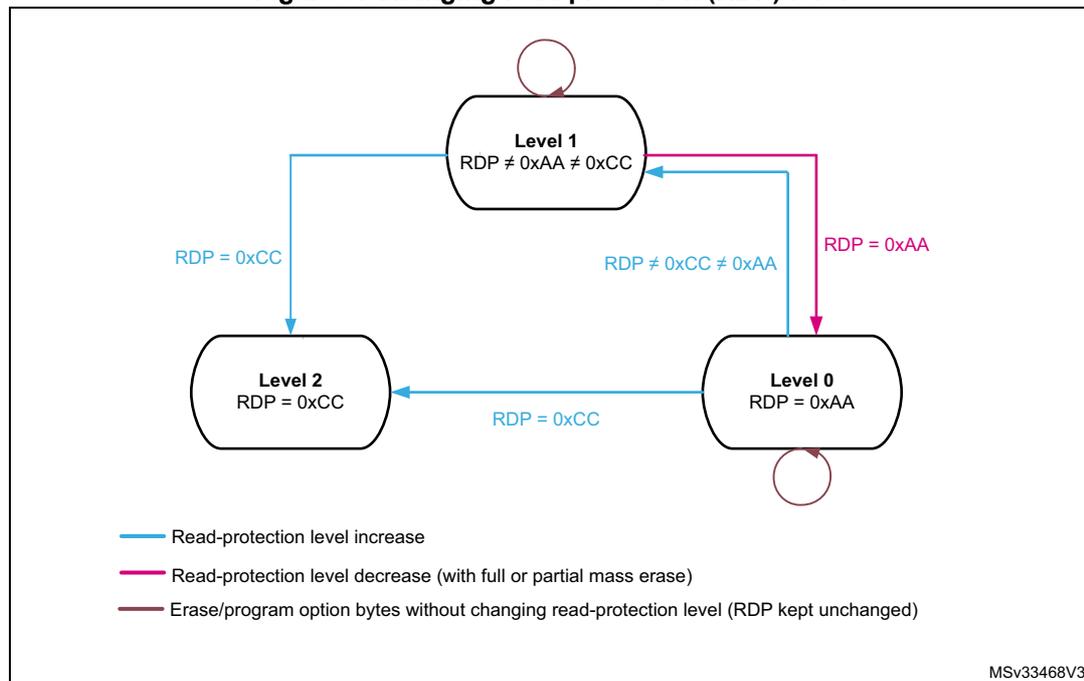
Table 14. Access status versus protection level and execution modes
| Area | Protection level | User execution (BootFromFlash) | Debug/ BootFromRam/ BootFromLoader | ||||
|---|---|---|---|---|---|---|---|
| Read | Write | Erase | Read | Write | Erase | ||
| Main Flash memory | 1 | Yes | Yes | Yes | No | No | No (3) |
| 2 | Yes | Yes | Yes | N/A (1) | N/A (1) | N/A (1) | |
| System memory (2) | 1 | Yes | No | No | Yes | No | No |
| 2 | Yes | No | No | N/A (1) | N/A (1) | N/A (1) | |
Table 14. Access status versus protection level and execution modes (continued)
| Area | Protection level | User execution (BootFromFlash) | Debug/ BootFromRam/ BootFromLoader | ||||
|---|---|---|---|---|---|---|---|
| Read | Write | Erase | Read | Write | Erase | ||
| Option bytes | 1 | Yes | Yes (3) | Yes | Yes | Yes (3) | Yes |
| 2 | Yes | No | No | N/A (1) | N/A (1) | N/A (1) | |
| Backup registers | 1 | Yes | Yes | N/A | No | No | No (4) |
| 2 | Yes | Yes | N/A | N/A (1) | N/A (1) | N/A (1) | |
| OTP | 1 | Yes | Yes | N/A | No | No | N/A |
| 2 | Yes | Yes | N/A | N/A (1) | N/A (1) | N/A (1) | |
- 1. When the protection Level 2 is active, the Debug port, the boot from RAM and the boot from System memory are disabled.
- 2. The System memory is only read-accessible, whatever the protection level (0, 1 or 2) and execution mode.
- 3. The Flash Main memory is erased when the RDP option byte is programmed with all level of protections disabled (0xAA).
- 4. The backup registers are erased when RDP changes from Level 1 to Level 0.
3.5.2 FLASH write protection (WRP)
The user area in Flash memory can be protected against unwanted write operations. Two write-protected (WRP) areas can be defined, with page (2-Kbyte) granularity. Each area is defined by a start page offset and an end page offset related to the physical Flash memory base address. These offsets are defined in the WRP address registers FLASH WRP area A address register (FLASH_WRP1AR) and FLASH WRP area B address register (FLASH_WRP1BR) , and, for dual-bank devices, also FLASH WRP2 area A address register (FLASH_WRP2AR) and FLASH WRP2 area B address register (FLASH_WRP2BR) .
The WRP x area ( x = A, B) of bank y ( y = 1 or 2) is defined from the address
Flash memory Base address + [WRPyx_STRT x 0x0800] (included)
to the address
Flash memory Base address + [(WRPyx_END+1) x 0x0800] (excluded).
The minimum WRP area size is one WRP page (2 Kbytes):
WRPyx_END = WRPyx_STRT .
For example, to protect the Bank 1 of Flash memory by WRP from the address 0x0800 1000 (included) to the address 0x0800 3FFF (included):
If boot in Flash memory is selected, FLASH_WRP1AR register must be programmed with:
- – WRP1A_STRT = 0x02.
- – WRP1A_END = 0x07.
WRP1B_STRT and WRP1B_END in FLASH_WRP1BR can be used instead (area B in Flash memory).
When WRP is active, it cannot be erased or programmed. Consequently, a software mass erase cannot be performed if one area is write-protected.
If an erase/program operation to a write-protected part of the Flash memory is attempted, the write protection error flag (WRPERR) of the FLASH_SR register is set. This flag is also set for any write access to:
- – OTP area
- – part of the Flash memory that can never be written like the ICP
Note: When the Flash memory read protection level is selected (RDP level = 1), it is not possible to program or erase the memory if the CPU debug features are connected (single wire) or boot code is being executed from SRAM or system Flash memory, even if WRP is not activated. Any attempt generates a hard fault (BusFault).
Table 15: WRP protection
| WRP registers values (x = A or B, y= 1 or 2) | WRP-protected area |
|---|---|
| WRPyx_STRT = WRPyx_END | Page WRPyx |
| WRPyx_STRT > WRPyx_END | None (unprotected) |
| WRPyx_STRT < WRPyx_END | Pages from WRPyx_STRT to WRPyx_END |
Note: To validate the WRP options, the option bytes must be reloaded by setting the OBL_LAUNCH bit in Flash memory control register.
3.6 FLASH interrupts
Table 16. FLASH interrupt requests
| Interrupt event | Event flag | Event flag/interrupt clearing method | Interrupt enable control bit |
|---|---|---|---|
| End of operation | EOP (1) | Write EOP=1 | EOPIE |
| Operation error | OPERR (2) | Write OPERR=1 | ERRIE |
| Write protection error | WRPERR | Write WRPERR=1 | N/A |
| Size error | SIZERR | Write SIZERR=1 | N/A |
| Programming sequential error | PROGERR | Write PROGERR=1 | N/A |
| Programming alignment error | PGAERR | Write PGAERR=1 | N/A |
| Programming sequence error | PGSERR | Write PGSERR=1 | N/A |
| Data miss during fast programming error | MISSERR | Write MISSERR=1 | N/A |
| Fast programming error | FASTERR | Write FASTERR=1 | N/A |
| ECC error correction | ECCC | Write ECCC=1 | ECCIE |
| ECC double error (NMI) | ECCD | Write ECCD=1 | N/A |
1. EOP is set only if EOPIE is set.
2. OPERR is set only if ERRIE is set.
3.7 FLASH registers
3.7.1 FLASH access control register (FLASH_ACR)
Address offset: 0x000
Reset value: 0x0004 0600
| 31 | 30 | 29 | 28 | 27 | 26 | 25 | 24 | 23 | 22 | 21 | 20 | 19 | 18 | 17 | 16 |
|---|---|---|---|---|---|---|---|---|---|---|---|---|---|---|---|
| Res. | Res. | Res. | Res. | Res. | Res. | Res. | Res. | Res. | Res. | Res. | Res. | Res. | Res. | Res. | EMPTY |
| 15 | 14 | 13 | 12 | 11 | 10 | 9 | 8 | 7 | 6 | 5 | 4 | 3 | 2 | 1 | 0 |
| Res. | Res. | Res. | Res. | ICRST | Res. | ICEN | PRFTEN | Res. | Res. | Res. | Res. | Res. | LATENCY[2:0] | ||
| rw | rw | rw | rw | rw | rw | ||||||||||
Bits 31:17 Reserved, must be kept at reset value.
Bit 16 EMPTY : Main Flash memory area empty
This bit indicates whether the first location of the Main Flash memory area is erased or has a programmed value.
0: Main Flash memory area programmed
1: Main Flash memory area empty
The bit can be set and reset by software.
Bits 15:12 Reserved, must be kept at reset value.
Bit 11 ICRST : CPU Instruction cache reset
0: CPU Instruction cache is not reset
1: CPU Instruction cache is reset
This bit can be written only when the instruction cache is disabled.
Bit 10 Reserved, must be kept at reset value.
Bit 9 ICEN : CPU Instruction cache enable
0: CPU Instruction cache is disabled
1: CPU Instruction cache is enabled
Bit 8 PRFTEN : CPU Prefetch enable
0: CPU Prefetch disabled
1: CPU Prefetch enabled
Bits 7:3 Reserved, must be kept at reset value.
Bits 2:0 LATENCY[2:0] : Flash memory access latency
The value in this bitfield represents the ratio of the HCLK clock period to the Flash memory access time.
000: Zero wait states
001: One wait state
010: Two wait states
Others: Reserved
A new write into the bitfield becomes effective when it returns the same value upon read.
3.7.2 FLASH key register (FLASH_KEYR)
Address offset: 0x008
Reset value: 0x0000 0000
| 31 | 30 | 29 | 28 | 27 | 26 | 25 | 24 | 23 | 22 | 21 | 20 | 19 | 18 | 17 | 16 |
|---|---|---|---|---|---|---|---|---|---|---|---|---|---|---|---|
| KEY[31:16] | |||||||||||||||
| w | w | w | w | w | w | w | w | w | w | w | w | w | w | w | w |
| 15 | 14 | 13 | 12 | 11 | 10 | 9 | 8 | 7 | 6 | 5 | 4 | 3 | 2 | 1 | 0 |
| KEY[15:0] | |||||||||||||||
| w | w | w | w | w | w | w | w | w | w | w | w | w | w | w | w |
Bits 31:0 KEY[31:0] : FLASH key
The following values must be written consecutively to unlock the FLASH control register (FLASH_CR) , thus enabling programming/erasing operations:
KEY1: 0x4567 0123
KEY2: 0xCDEF 89AB
3.7.3 FLASH option key register (FLASH_OPTKEYR)
Address offset: 0x00C
Reset value: 0x0000 0000
| 31 | 30 | 29 | 28 | 27 | 26 | 25 | 24 | 23 | 22 | 21 | 20 | 19 | 18 | 17 | 16 |
|---|---|---|---|---|---|---|---|---|---|---|---|---|---|---|---|
| OPTKEY[31:16] | |||||||||||||||
| w | w | w | w | w | w | w | w | w | w | w | w | w | w | w | w |
| 15 | 14 | 13 | 12 | 11 | 10 | 9 | 8 | 7 | 6 | 5 | 4 | 3 | 2 | 1 | 0 |
| OPTKEY[15:0] | |||||||||||||||
| w | w | w | w | w | w | w | w | w | w | w | w | w | w | w | w |
Bits 31:0 OPTKEY[31:0] : Option byte key
The following values must be written consecutively to unlock the Flash memory option registers, enabling option byte programming/erasing operations:
KEY1: 0x0819 2A3B
KEY2: 0x4C5D 6E7F
3.7.4 FLASH status register (FLASH_SR)
Address offset: 0x010
Reset value: 0x000X 0000
| 31 | 30 | 29 | 28 | 27 | 26 | 25 | 24 | 23 | 22 | 21 | 20 | 19 | 18 | 17 | 16 |
|---|---|---|---|---|---|---|---|---|---|---|---|---|---|---|---|
| Res. | Res. | Res. | Res. | Res. | Res. | Res. | Res. | Res. | Res. | Res. | Res. | Res. | CFGBSY | BSY2 | BSY1 |
| r | r | r | |||||||||||||
| 15 | 14 | 13 | 12 | 11 | 10 | 9 | 8 | 7 | 6 | 5 | 4 | 3 | 2 | 1 | 0 |
| OPTV ERR | Res. | Res. | Res. | Res. | Res. | FAST ERR | MISS ERR | PGS ERR | SIZ ERR | PGA ERR | WRP ERR | PROG ERR | Res. | OP ERR | EOP |
| rc_w1 | rc_w1 | rc_w1 | rc_w1 | rc_w1 | rc_w1 | rc_w1 | rc_w1 | rc_w1 | rc_w1 |
Bits 31:19 Reserved, must be kept at reset value.
Bit 18 CFGBSY : Programming or erase configuration busy.
This flag is set and reset by hardware. (set when first word is sent and reset when program operation completes or is interrupted by an error.)
When set to 1 the programming and erase settings in requested by FLASH control register (FLASH_CR) are used (busy), and cannot be changed (a programming or erase operation is ongoing).
When reset to 0 programming and erase settings in in FLASH control register (FLASH_CR) can be modified.
Bit 17 BSY2 : Busy
This flag indicates that a Flash memory Bank 2 operation requested by FLASH control register (FLASH_CR) is in progress. This bit is set at the beginning of the Flash memory operation, and cleared when the operation finishes or when an error occurs.
Bit 16 BSY1 : Busy
This flag indicates that a Flash memory (Bank 1 for dual-bank devices) operation requested by FLASH control register (FLASH_CR) is in progress. This bit is set at the beginning of the Flash memory operation, and cleared when the operation finishes or when an error occurs.
Bit 15 OPTVERR : Option and Engineering bits loading validity error
Set by hardware when the options and engineering bits read may not be the one configured by the user or production. If options and engineering bits haven't been properly loaded, OPTVERR is set again after each system reset. Option bytes that fail loading are forced to a safe value, see Section 3.4.2: FLASH option byte programming .
Cleared by writing 1.
Bits 14:10 Reserved, must be kept at reset value.
Bit 9 FASTERR : Fast programming error
Set by hardware when a fast programming sequence (activated by FSTPG) is interrupted due to an error (alignment, size, write protection or data miss). The corresponding status bit (PGAERR, SIZERR, WRPERR or MISSERR) is set at the same time.
Cleared by writing 1.
Bit 8 MISSERR : Fast programming data miss error
In Fast programming mode, 32 double words (256 bytes) must be sent to Flash memory successively, and the new data must be sent to the logic control before the current data is fully programmed. MISSERR is set by hardware when the new data is not present in time.
Cleared by writing 1.
Bit 7 PGSERR : Programming sequence error
Set by hardware when a write access to the Flash memory is performed by the code while PG or FSTPG have not been set previously. Set also by hardware when PROGERR, SIZERR, PGAERR, WRPERR, MISSERR or FASTERR is set due to a previous programming error.
Cleared by writing 1.
Bit 6 SIZERR : Size error
Set by hardware when the size of the access is a byte or half-word during a program or a fast program sequence. Only double word programming is allowed (consequently: word access).
Cleared by writing 1.
Bit 5 PGAERR : Programming alignment error
Set by hardware when the data to program cannot be contained in the same double word (64-bit) Flash memory in case of standard programming, or if there is a change of page during fast programming.
Cleared by writing 1.
Bit 4 WRPERR : Write protection error
Set by hardware when an address to be erased/programmed belongs to a write-protected part (by WRP or RDP Level 1) of the Flash memory.
Cleared by writing 1.
Bit 3 PROGERR : Programming error
Set by hardware when a double-word address to be programmed contains a value different from '0xFFFF FFFF' before programming, except if the data to write is '0x0000 0000'.
Cleared by writing 1.
Bit 2 Reserved, must be kept at reset value.
Bit 1 OPERR : Operation error
Set by hardware when a Flash memory operation (program / erase) completes unsuccessfully.
This bit is set only if error interrupts are enabled (ERRIE=1).
Cleared by writing '1'.
Bit 0 EOP : End of operation
Set by hardware when one or more Flash memory operation (programming / erase) has been completed successfully.
This bit is set only if the end of operation interrupts are enabled (EOPIE=1).
Cleared by writing 1.
3.7.5 FLASH control register (FLASH_CR)
Address offset: 0x014
Reset value: 0xC000 0000
Access: no wait state when no Flash memory operation is on going, word, half-word and byte access
This register cannot be modified when CFGBSY in FLASH status register (FLASH_SR) is set.
| 31 | 30 | 29 | 28 | 27 | 26 | 25 | 24 | 23 | 22 | 21 | 20 | 19 | 18 | 17 | 16 |
|---|---|---|---|---|---|---|---|---|---|---|---|---|---|---|---|
| LOCK | OPT LOCK | Res. | Res. | OBL LAUNCH | Res. | ERRIE | EOPIE | Res. | Res. | Res. | Res. | Res. | FSTPG | OPT STRT | STRT |
| rs | rs | rc_w1 | rw | rw | rw | rs | rs | ||||||||
| 15 | 14 | 13 | 12 | 11 | 10 | 9 | 8 | 7 | 6 | 5 | 4 | 3 | 2 | 1 | 0 |
| MER2 | Res. | BKER | PNB[9:0] | MER1 | PER | PG | |||||||||
| rw | rw | rw | rw | rw | rw | rw | rw | rw | rw | rw | rw | rw | rw | rw | |
Bit 31 LOCK : FLASH_CR Lock
This bit is set only. When set, the FLASH_CR register is locked. It is cleared by hardware after detecting the unlock sequence.
In case of an unsuccessful unlock operation, this bit remains set until the next system reset.
Bit 30 OPTLOCK : Options Lock
This bit is set only. When set, all bits concerning user option in FLASH_CR register and so option page are locked. This bit is cleared by hardware after detecting the unlock sequence. The LOCK bit must be cleared before doing the unlock sequence for OPTLOCK bit.
In case of an unsuccessful unlock operation, this bit remains set until the next reset.
Bits 29:28 Reserved, must be kept at reset value.
Bit 27 OBL_LAUNCH : Option byte load launch
When set, this bit triggers the load of option bytes into option registers. It is automatically cleared upon the completion of the load. The high state of the bit indicates pending option byte load.
The bit cannot be cleared by software. It cannot be written as long as OPTLOCK is set.
Bit 26 Reserved, must be kept at reset value.
Bit 25 ERRIE : Error interrupt enable
This bit enables the interrupt generation upon setting the OPERR flag in the FLASH_SR register.
0: Disable
1: Enable
Bit 24 EOPIE : End-of-operation interrupt enable
This bit enables the interrupt generation upon setting the EOP flag in the FLASH_SR register.
0: Disable
1: Enable
Bits 23:19 Reserved, must be kept at reset value.
Bit 18 FSTPG : Fast programming enable
0: Disable
1: Enable
Bit 17 OPTSTR : Start of modification of option bytes
This bit triggers an options operation when set.
This bit is set only by software, and is cleared when the BSY1 bit is cleared in FLASH_SR.
Bit 16 STRT : Start erase operation
This bit triggers an erase operation when set.
This bit is possible to set only by software and to clear only by hardware. The hardware clears it when one of BSY1 and BSY2 flags in the FLASH_SR register transits to zero.
Bit 15 MER2 : Mass erase, Bank 2
When set, this bit triggers the mass erase of Bank 2 (all user pages).
Bits 14 Reserved, must be kept at reset value.
Bit 13 BKER : Bank selection for erase operation
This bit selects the target of erase operation (Bank 1 or Bank 2).
0: Bank 1
1: Bank 2
The bit has no effect on the single-bank devices.
Bits 12:3 PNB[9:0] : Page number selection
These bits select the page to erase:
0x00: page 0
0x01: page 1
...
0x17F: page 383
Note: Values corresponding to addresses outside the Main memory are not allowed.
Bit 2 MER1 : Mass erase (Bank 1)
When set, this bit triggers the mass erase, that is, all user pages (of Bank 1 for dual-bank devices).
Bit 1 PER : Page erase enable
0: Disable
1: Enable
Bit 0 PG : Flash memory programming enable
0: Disable
1: Enable
3.7.6 FLASH ECC register (FLASH_ECCR)
Address offset: 0x018
Reset value: 0x0000 0000
Access: no wait state when no Flash memory operation is on going, word, half-word and byte access
This register applies to single-bank products and to Bank 1 of dual-bank products.
Bit 31 ECCD : ECC detection
Set by hardware when two ECC errors have been detected. When this bit is set, a NMI is generated.
Cleared by writing 1.
Bit 30 ECCC : ECC correction
Set by hardware when one ECC error has been detected and corrected. An interrupt is generated if ECCIE is set.
Cleared by writing 1.
Bits 29:25 Reserved, must be kept at reset value.
Bit 24 ECCIE : ECC correction interrupt enable
0: ECCC interrupt disabled
1: ECCC interrupt enabled
Bits 23:21 Reserved, must be kept at reset value.
Bit 20 SYSF_ECC : System Flash memory ECC fail
This bit indicates that the ECC error correction or double ECC error detection is located in the system Flash memory.
Bits 19:14 Reserved, must be kept at reset value.
Bits 13:0 ADDR_ECC[13:0] : ECC fail double-word address offset
In case of ECC error or ECC correction detected, this bitfield contains double-word offset (multiple of 64 bits) to Main Flash memory.
3.7.7 FLASH ECC register 2 (FLASH_ECCR2)
Address offset: 0x01C
Reset value: 0x0000 0000
Access: no wait state when no Flash memory operation is on going, word, half-word and byte access
This register applies to Bank 2 of dual-bank products.
Bit 31 ECCD : ECC detection
Set by hardware when two ECC errors have been detected. When this bit is set, a NMI is generated.
Cleared by writing 1.
Bit 30 ECCC : ECC correction
Set by hardware when one ECC error has been detected and corrected. An interrupt is generated if ECCIE is set.
Cleared by writing 1.
Bits 29:25 Reserved, must be kept at reset value.
Bit 24 ECCIE : ECC correction interrupt enable
0: ECCC interrupt disabled
1: ECCC interrupt enabled
Bits 23:21 Reserved, must be kept at reset value.
Bit 20 SYSF_ECC : System Flash memory ECC fail
This bit indicates that the ECC error correction or double ECC error detection is located in the system Flash memory.
Bits 19:14 Reserved, must be kept at reset value.
Bits 13:0 ADDR_ECC[13:0] : ECC fail double-word address offset
In case of ECC error or ECC correction detected, this bitfield contains double-word offset (multiple of 64 bits) to Main Flash memory.
3.7.8 FLASH option register (FLASH_OPTR)
Address offset: 0x020
Reset value: 0b1101 1XXX 1X1X XXXX 1XX0 0001 XXXX XXXX (The option bits are loaded with values from Flash memory at power-on reset release.)
Access: no wait state when no Flash memory operation is on going, word, half-word and byte access
| 31 | 30 | 29 | 28 | 27 | 26 | 25 | 24 | 23 | 22 | 21 | 20 | 19 | 18 | 17 | 16 |
|---|---|---|---|---|---|---|---|---|---|---|---|---|---|---|---|
| Res. | Res. | Res. | Res. | Res. | n BOOT0 | n BOOT1 | nBOOT _SEL | Res. | RAM PARITY CHECK | DUAL_ BANK | SWAP _BANK | WWDG _SW | IWGD _ STDBY | IWDG _STOP | IWDG _SW |
| rw | rw | rw | rw | rw | rw | rw | rw | rw | rw | ||||||
| 15 | 14 | 13 | 12 | 11 | 10 | 9 | 8 | 7 | 6 | 5 | 4 | 3 | 2 | 1 | 0 |
| Res. | nRST_ STDBY | nRST_ STOP | Res. | Res. | Res. | Res. | Res. | RDP[7:0] | |||||||
| rw | rw | rw | rw | rw | rw | rw | rw | rw | rw | ||||||
Bits 31:27 Reserved, must be kept at reset value.
Bit 26 nBOOT0 : nBOOT0 option bit
0: nBOOT0=0
1: nBOOT0=1
Bit 25 nBOOT1 : Boot configuration
Together with the BOOT0 pin or option bit nBOOT0 (depending on nBOOT_SEL option bit configuration), this bit selects boot mode from the Main Flash memory, SRAM or the System memory. Refer to Section 2.5: Boot configuration
Bit 24 nBOOT_SEL
0: BOOT0 signal is defined by BOOT0 pin value (legacy mode)
1: BOOT0 signal is defined by nBOOT0 option bit
Bit 23 Reserved, must be kept at reset value.
Bit 22 RAM_PARITY_CHECK : SRAM parity check control
0: SRAM parity check enable
1: SRAM parity check disable
Bit 21 DUAL_BANK : Dual-bank on 512 Kbytes or 256 Kbytes Flash memory devices
0: 256 Kbytes/512 Kbytes single-bank Flash memory, contiguous addresses in Bank 1
1: 256 Kbytes/512 Kbytes dual-bank Flash memory, Refer to
Table 9
Bit 20 nSWAP_BANK : Empty check boot configuration
This bit selects the bank that is the subject of empty check upon boot.
0: Bank 1
1: Bank 2
Bit 19 WWDG_SW : Window watchdog selection
0: Hardware window watchdog
1: Software window watchdog
Bit 18 IWDG_STDBY : Independent watchdog counter freeze in Standby mode
0: Independent watchdog counter is frozen in Standby mode
1: Independent watchdog counter is running in Standby mode
Bit 17 IWDG_STOP : Independent watchdog counter freeze in Stop mode
0: Independent watchdog counter is frozen in Stop mode
1: Independent watchdog counter is running in Stop mode
Bit 16 IDWG_SW : Independent watchdog selection
0: Hardware independent watchdog
1: Software independent watchdog
Bit 15 Reserved, must be kept at reset value.
Bit 14 nRST_STDBY
0: Reset generated when entering the Standby mode
1: No reset generated when entering the Standby mode
Bit 13 nRST_STOP
0: Reset generated when entering the Stop mode
1: No reset generated when entering the Stop mode
Bits 12:8 Reserved, must be kept at reset value.
Bits 7:0 RDP[7:0] : Read protection level
Note: 0xAA: Level 0, read protection not active
0xCC: Level 2, chip read protection active
Others: Level 1, memories read protection active
3.7.9 FLASH WRP area A address register (FLASH_WRP1AR)
Address offset: 0x02C
Reset value: 0x00XX 00XX (The option bits are loaded with values from Flash memory at power-on reset release.)
Access: no wait state when no Flash memory operation is on going, word, half-word and byte access.
| 31 | 30 | 29 | 28 | 27 | 26 | 25 | 24 | 23 | 22 | 21 | 20 | 19 | 18 | 17 | 16 |
|---|---|---|---|---|---|---|---|---|---|---|---|---|---|---|---|
| Res. | Res. | Res. | Res. | Res. | Res. | Res. | Res. | Res. | WRP1A_END[6:0] | ||||||
| rw | rw | rw | rw | rw | rw | rw | |||||||||
| 15 | 14 | 13 | 12 | 11 | 10 | 9 | 8 | 7 | 6 | 5 | 4 | 3 | 2 | 1 | 0 |
| Res. | Res. | Res. | Res. | Res. | Res. | Res. | Res. | Res. | WRP1A_STR[6:0] | ||||||
| rw | rw | rw | rw | rw | rw | rw | |||||||||
Bits 31:23 Reserved, must be kept at reset value.
Bits 22:16 WRP1A_END[6:0] : WRP area A end offset (Bank 1)
This bitfield contains the offset of the last page of the WRP area A (in Bank 1 for dual-bank devices). (1)
Bits 15:6 Reserved, must be kept at reset value.
Bits 6:0 WRP1A_STR[6:0] : WRP area A start offset (Bank 1)
This bitfield contains the offset of the first page of the WRP area A (in Bank 1 for dual-bank devices). (1)
- 1. The number of effective bits depends on the size of Flash memory in the device.
3.7.10 FLASH WRP area B address register (FLASH_WRP1BR)
Address offset: 0x030
Reset value: 0b0000 0000 0XXX XXXX 0000 0000 0XXX XXXX (The option bits are loaded with values from Flash memory at power-on reset release.)
Access: no wait state when no Flash memory operation is on going, word, half-word and byte access.
| 31 | 30 | 29 | 28 | 27 | 26 | 25 | 24 | 23 | 22 | 21 | 20 | 19 | 18 | 17 | 16 |
|---|---|---|---|---|---|---|---|---|---|---|---|---|---|---|---|
| Res. | Res. | Res. | Res. | Res. | Res. | Res. | Res. | Res. | WRP1B_END[6:0] | ||||||
| rw | rw | rw | rw | rw | rw | rw | |||||||||
| 15 | 14 | 13 | 12 | 11 | 10 | 9 | 8 | 7 | 6 | 5 | 4 | 3 | 2 | 1 | 0 |
| Res. | Res. | Res. | Res. | Res. | Res. | Res. | Res. | Res. | WRP1B_STR[6:0] | ||||||
| rw | rw | rw | rw | rw | rw | rw | |||||||||
Bits 31:23 Reserved, must be kept at reset value.
Bits 22:16 WRP1B_END[6:0] : WRP area B end offset (Bank 1)
This bitfield contains the offset of the last page of the WRP area B (in Bank 1 for dual-bank devices). (1)
Bits 15:7 Reserved, must be kept at reset value.
Bits 6:0 WRP1B_STRT[6:0] : WRP area B start offset (Bank 1)
This bitfield contains the offset of the first page of the WRP area B (in Bank 1 for dual-bank devices). (1)
- 1. The number of effective bits depends on the size of Flash memory in the device.
3.7.11 FLASH WRP2 area A address register (FLASH_WRP2AR)
Address offset: 0x04C
Reset value: 0b0000 0000 0XXX XXXX 0000 0000 0XXX XXXX (The option bits are loaded with values from Flash memory at power-on reset release.)
Access: no wait state when no Flash memory operation is on going, word, half-word and byte access.
| 31 | 30 | 29 | 28 | 27 | 26 | 25 | 24 | 23 | 22 | 21 | 20 | 19 | 18 | 17 | 16 |
|---|---|---|---|---|---|---|---|---|---|---|---|---|---|---|---|
| Res. | Res. | Res. | Res. | Res. | Res. | Res. | Res. | Res. | WRP2A_END[6:0] | ||||||
| rw | rw | rw | rw | rw | rw | rw | |||||||||
| 15 | 14 | 13 | 12 | 11 | 10 | 9 | 8 | 7 | 6 | 5 | 4 | 3 | 2 | 1 | 0 |
| Res. | Res. | Res. | Res. | Res. | Res. | Res. | Res. | Res. | WRP2A_STRT[6:0] | ||||||
| rw | rw | rw | rw | rw | rw | rw | |||||||||
Bits 31:23 Reserved, must be kept at reset value.
Bits 22:16 WRP2A_END[6:0] : WRP area A end offset, Bank 2
This bitfield contains the offset of the last page of the WRP area A in Bank 2. (1)
Bits 15:7 Reserved, must be kept at reset value.
Bits 6:0 WRP2A_STRT[6:0] : WRP area A start offset, Bank 2
This bitfield contains the offset of the first page of the WRP area A in Bank 2. (1)
- 1. The number of effective bits depends on the size of Flash memory in the device.
3.7.12 FLASH WRP2 area B address register (FLASH_WRP2BR)
Address offset: 0x050
Reset value: 0b0000 0000 0XXX XXXX 0000 0000 0XXX XXXX (The option bits are loaded with values from Flash memory at power-on reset release.)
Access: no wait state when no Flash memory operation is on going, word, half-word and byte access.
| 31 | 30 | 29 | 28 | 27 | 26 | 25 | 24 | 23 | 22 | 21 | 20 | 19 | 18 | 17 | 16 |
|---|---|---|---|---|---|---|---|---|---|---|---|---|---|---|---|
| Res. | Res. | Res. | Res. | Res. | Res. | Res. | Res. | Res. | WRP2B_END[6:0] | ||||||
| rw | rw | rw | rw | rw | rw | rw | |||||||||
| 15 | 14 | 13 | 12 | 11 | 10 | 9 | 8 | 7 | 6 | 5 | 4 | 3 | 2 | 1 | 0 |
| Res. | Res. | Res. | Res. | Res. | Res. | Res. | Res. | Res. | WRP2B_STRT[6:0] | ||||||
| rw | rw | rw | rw | rw | rw | rw | |||||||||
Bits 31:23 Reserved, must be kept at reset value.
Bits 22:16 WRP2B_END[6:0] : WRP area B end offset, Bank 2
This bitfield contains the offset of the last page of the WRP area B in Bank 2. (1)
Bits 15:7 Reserved, must be kept at reset value.
Bits 6:0 WRP2B_STRT[6:0] : WRP area B start offset, Bank 2
This bitfield contains the offset of the first page of the WRP area B in Bank 2. (1)
1. The number of effective bits depends on the size of Flash memory in the device.
3.7.13 FLASH register map
Table 17. FLASH register map and reset values
| Offset | Register | 31 | 30 | 29 | 28 | 27 | 26 | 25 | 24 | 23 | 22 | 21 | 20 | 19 | 18 | 17 | 16 | 15 | 14 | 13 | 12 | 11 | 10 | 9 | 8 | 7 | 6 | 5 | 4 | 3 | 2 | 1 | 0 |
|---|---|---|---|---|---|---|---|---|---|---|---|---|---|---|---|---|---|---|---|---|---|---|---|---|---|---|---|---|---|---|---|---|---|
| 0x000 | FLASH_ACR | Res | Res | Res | Res | Res | Res | Res | Res | Res | Res | Res | Res | Res | Res | Res | EMPTY | Res | Res | Res | Res | ICRST | Res | ICEN | PRFTEN | Res | Res | Res | Res | Res | Res | LATENCY [2:0] | |
| Reset value | X | 0 | 1 | 0 | 0 0 0 | ||||||||||||||||||||||||||||
| 0x004 | Reserved | Res | Res | Res | Res | Res | Res | Res | Res | Res | Res | Res | Res | Res | Res | Res | Res | Res | Res | Res | Res | Res | Res | Res | Res | Res | Res | Res | Res | Res | Res | Res | |
| Reset value | |||||||||||||||||||||||||||||||||
| 0x008 | FLASH_KEYR | KEYR[31:0] | |||||||||||||||||||||||||||||||
| Reset value | 0 | 0 | 0 | 0 | 0 | 0 | 0 | 0 | 0 | 0 | 0 | 0 | 0 | 0 | 0 | 0 | 0 | 0 | 0 | 0 | 0 | 0 | 0 | 0 | 0 | 0 | 0 | 0 | 0 | 0 | 0 | ||
| 0x00C | FLASH_OPT_KEYR | OPTKEY[31:0] | |||||||||||||||||||||||||||||||
| Reset value | 0 | 0 | 0 | 0 | 0 | 0 | 0 | 0 | 0 | 0 | 0 | 0 | 0 | 0 | 0 | 0 | 0 | 0 | 0 | 0 | 0 | 0 | 0 | 0 | 0 | 0 | 0 | 0 | 0 | 0 | 0 | ||
| 0x010 | FLASH_SR | Res | Res | Res | Res | Res | Res | Res | Res | Res | Res | Res | Res | Res | CFGBSY | BSY2 | BSY1 | OPTVERR | Res | Res | Res | Res | Res | FASTERR | MISERR | PGSERR | SIZERR | PGAERR | WRPERR | PROGERR | Res | OPERR | EOP |
| Reset value | 0 | 0 | 0 | X | 0 | 0 | 0 | 0 | 0 | 0 | 0 | 0 0 | |||||||||||||||||||||
| 0x014 | FLASH_CR | LOCK | OPTLOCK | Res | Res | OBL_LAUNCH | Res | ERRIE | EOPIE | Res | Res | Res | Res | Res | FSTPG | OPTSTRT | STR | MER2 | Res | BKER | PNB[9:0] | MER1 | PER | PG | |||||||||
| Reset value | 1 | 1 | 0 | 0 | 0 | 0 | 0 | 0 | 0 | 0 | 0 | 0 | 0 | 0 | 0 | 0 | 0 | 0 | 0 | 0 | 0 | ||||||||||||
| 0x018 | FLASH_ECCR | ECCD | ECCC | Res | Res | Res | Res | ECCIE | Res | Res | Res | Res | Res | Res | Res | Res | Res | Res | Res | Res | ADDR_ECC[13:0] | ||||||||||||
| Reset value | 0 | 0 | 0 | 0 | 0 | 0 | 0 | 0 | 0 | 0 | 0 | 0 | 0 | 0 | 0 | ||||||||||||||||||
| 0x020 | FLASH_OPTR | Res | Res | Res | Res | nBOOT0 | nBOOT1 | nBOOT_SEL | Res | RAM_PARITY_CHECK | DUAL_BANK | Res | WWDG_SW | IWDG_STBY | IWDG_STOP | IWDG_SW | nRST_STDBY | nRST_STOP | Res | Res | Res | Res | Res | Res | Res | Res | RDP[7:0] | ||||||
| Reset value | X | X | X | X | X | X | X | X | X | X | X | X | X | X | X | X | X | X | X | X | |||||||||||||
| 0x024 - 0x02B | Reserved | Res | Res | Res | Res | Res | Res | Res | Res | Res | Res | Res | Res | Res | Res | Res | Res | Res | Res | Res | Res | Res | Res | Res | Res | Res | Res | Res | Res | Res | Res | Res | |
| 0x02C | FLASH_WRP1AR | Res | Res | Res | Res | Res | Res | Res | Res | WRP1A_END[6:0] | Res | Res | Res | Res | Res | Res | Res | Res | Res | Res | WRP1A_STR[6:0] | ||||||||||||
| Reset value | X | X | X | X | X | X | X | X | X | X | X | X | X | X | |||||||||||||||||||
| 0x030 | FLASH_WRP1BR | Res | Res | Res | Res | Res | Res | Res | Res | WRP1B_END[6:0] | Res | Res | Res | Res | Res | Res | Res | Res | Res | Res | WRP1B_STR[6:0] | ||||||||||||
| Reset value | X | X | X | X | X | X | X | X | X | X | X | X | X | X | |||||||||||||||||||
| 0x04C | FLASH_WRP2AR | Res | Res | Res | Res | Res | Res | Res | Res | WRP2A_END[6:0] | Res | Res | Res | Res | Res | Res | Res | Res | Res | Res | WRP2A_STR[6:0] | ||||||||||||
| Reset value | X | X | X | X | X | X | X | X | X | X | X | X | X | X | |||||||||||||||||||
| 0x050 | FLASH_WRP2BR | Res | Res | Res | Res | Res | Res | Res | Res | WRP2B_END[6:0] | Res | Res | Res | Res | Res | Res | Res | Res | Res | Res | WRP2B_STR[6:0] | ||||||||||||
| Reset value | X | X | X | X | X | X | X | X | X | X | X | X | X | X | |||||||||||||||||||
| 0x034 - 0x07F | Reserved | Res | Res | Res | Res | Res | Res | Res | Res | Res | Res | Res | Res | Res | Res | Res | Res | Res | Res | Res | Res | Res | Res | Res | Res | Res | Res | Res | Res | Res | Res | Res | |