16. Extended interrupts and event controller (EXTI)
The extended interrupts and event controller (EXTI) manages the individual CPU and system wake-up through configurable and direct event inputs. It provides wake-up requests to the power control and generates an interrupt request to the CPU NVIC and events to the CPU event input.
For each CPU, an additional event Generation block (EVG) is needed to generate the CPU event signal.
The EXTI wake-up requests allow the system to be woken up from Stop modes and the CPU to be woken up from the CStop and CStandby modes.
The interrupt request and event request generation can also be used in Run modes.
16.1 EXTI main features
The EXTI main features are the following:
- • 47 input events are supported.
- • Most event inputs allow the system to be waked up.
- • Some events can only be used to generate a CPU wake-up event.
- • Events which do not have an associated wake-up flag in the peripheral, have a flag in the EXTI and generate an interrupt to the CPU from the EXTI.
The asynchronous event inputs are classified in the following two groups:
- • Configurable events (signals from I/Os or peripherals able to generate a pulse), with features listed below:
- – Selectable active trigger edge
- – Interrupt pending status register bit
- – Individual interrupt and event generation mask, used for conditioning the CPU wake-up, interrupt and event generation
- – SW trigger possibility
- • Direct events (interrupt and wake-up sources from peripherals, having an associated flag to be cleared in the peripheral), with features listed below:
- – Fixed rising edge active trigger
- – No interrupt pending status register bit in the EXTI (The interrupt pending status flag is provided by the peripheral generating the event.)
- – Individual interrupt and event generation mask, used for conditioning the CPU wake-up and event generation
- – No software trigger possibility
16.2 EXTI block diagram
The EXTI consists of a register block accessed via an AHB interface, the event input trigger block and the masking block as shown in Figure 54 .
The register block contains all the EXTI registers.
The event input trigger block provides event input edge trigger logic.
The masking block provides the event input distribution to the different wake-up, interrupt and event outputs, and the masking of these.
Figure 54. EXTI block diagram
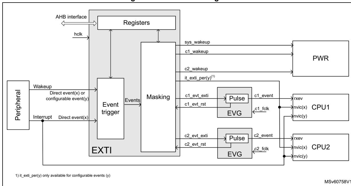
Table 91. EXTI pin overview
| Pin name | I/O | Description |
|---|---|---|
| AHB interface | I/O | EXTI register bus interface |
| hclk | I | AHB bus clock and EXTI system clock |
| Configurable event(y) | I | Asynchronous wake-up events from peripherals which do not have an associated interrupt and flag in the peripheral |
| Direct event(x) | I | Synchronous and asynchronous wake-up events from peripherals which have an associated interrupt and flag in the peripheral |
| it_exti_per (y) | O | Interrupts to the CPU associated with the configurable event (y) |
| cn_evt_exti | O | High-level sensitive event output for the CPU n , synchronous to hclk |
| cn_evt_rst | I | Asynchronous reset input to clear cn_evt_exti |
| sys_wakeup | O | Asynchronous system wake-up request to PWR for ck_sys and hclk |
| cn_wakeup | O | Wake-up request to PWR for the CPU n , synchronous to hclk |
Table 92. EVG pin overview
| Pin name | I/O | Description |
|---|---|---|
| cn_fclk | I | CPU n free running clock |
| cn_evt_in | I | High-level sensitive events input from EXTI, asynchronous to the CPU n clock |
| cn_event | O | Event pulse, synchronous to the CPU n clock |
| cn_evt_rst | O | Event reset signal, synchronous to the CPU n clock |
16.3 EXTI connections between peripherals and CPU
The peripherals able to generate wake-up or interrupt events when the system is in Stop mode, are connected to the EXTI.
Peripheral wake-up signals that generate a pulse or that do not have an interrupt status bits in the peripheral, are connected to an EXTI configurable event input. For these events, the EXTI provides a status pending bit which requires to be cleared. It is the EXTI interrupt associated with the status bit that interrupts the CPU.
Peripheral interrupt and wake-up signals that have a status bit in the peripheral which requires to be cleared in the peripheral, are connected to an EXTI direct event input. There is no status pending bit within the EXTI. The interrupt or wake-up is cleared by the CPU in the peripheral. It is the peripheral interrupt that interrupts the CPU directly.
The EXTI configurable event interrupts are connected to the NVIC of the CPU.
The dedicated EXTI/EVG CPU event is connected to the CPU rxev input.
The EXTI CPU wake-up signals are connected to the PWR block and are used to wake up the system and CPU sub-system bus clocks.
16.3.1 EXTI wake-up interrupt list
The wake-up sources are listed in Table 93: Wake-up interrupts .
Some wake-up sources are able to generate an event to the CPU (see 'Event' column).
The wake-up source capability to wake up a CPU is noted in wake-up column.
For CPU interrupt handling, see Section 15: Nested vectored interrupt controller (NVIC) .
Table 93. Wake-up interrupts
| EXTI n° | Acronym | Description | EXTI type | Event | Wake-up |
|---|---|---|---|---|---|
| 0 | EXTI[0] | EXTI line 0 from SYSCFG | Configurable | Yes | CPU1 and CPU2 |
| 1 | EXTI[1] | EXTI line 1 from SYSCFG | Configurable | Yes | CPU1 and CPU2 |
| 2 | EXTI[2] | EXTI line 2 from SYSCFG | Configurable | Yes | CPU1 and CPU2 |
| 3 | EXTI[3] | EXTI line 3 from SYSCFG | Configurable | Yes | CPU1 and CPU2 |
| 4 | EXTI[4] | EXTI line 4 from SYSCFG | Configurable | Yes | CPU1 and CPU2 |
| 5 | EXTI[5] | EXTI line 5 from SYSCFG | Configurable | Yes | CPU1 and CPU2 |
| 6 | EXTI[6] | EXTI line 6 from SYSCFG | Configurable | Yes | CPU1 and CPU2 |
| 7 | EXTI[7] | EXTI line 7 from SYSCFG | Configurable | Yes | CPU1 and CPU2 |
| 8 | EXTI[8] | EXTI line 8 from SYSCFG | Configurable | Yes | CPU1 and CPU2 |
| 9 | EXTI[8] | EXTI line 9 from SYSCFG | Configurable | Yes | CPU1 and CPU2 |
| 10 | EXTI[10] | EXTI line 10 from SYSCFG | Configurable | Yes | CPU1 and CPU2 |
| 11 | EXTI[11] | EXTI line 11 from SYSCFG | Configurable | Yes | CPU1 and CPU2 |
| 12 | EXTI[12] | EXTI line 12 from SYSCFG | Configurable | Yes | CPU1 and CPU2 |
| 13 | EXTI[13] | EXTI line 13 from SYSCFG | Configurable | Yes | CPU1 and CPU2 |
Table 93. Wake-up interrupts (continued)
| EXTI n° | Acronym | Description | EXTI type | Event | Wake-up |
|---|---|---|---|---|---|
| 14 | EXTI[14] | EXTI line 14 from SYSCFG | Configurable | Yes | CPU1 and CPU2 |
| 15 | EXTI[15] | EXTI line 15 from SYSCFG | Configurable | Yes | CPU1 and CPU2 |
| 16 | PVD | PVD line | Configurable | No | CPU1 and CPU2 |
| 17 | RTC_ALARM | RTC alarms A and B interrupt | Direct | Yes | CPU1 and CPU2 |
| 18 | SSRU | RTC SSR underflow interrupt | Direct | Yes | CPU1 and CPU2 |
| 19 | TAMP, RTC_STAMP, LSE_CSS | TAMP tamper interrupt RTC timestamp interrupt RCC LSECSS interrupt | Direct | Yes | CPU1 and CPU2 |
| 20 | RTC_WKUP | RTC wake-up interrupt | Direct | Yes | CPU1 and CPU2 |
| 21 | COMP1 | COMP1 line | Configurable | Yes | CPU1 and CPU2 |
| 22 | COMP2 | COMP2 line | Configurable | Yes | CPU1 and CPU2 |
| 23 | I2C1 wake-up | I2C1 wake-up | Direct | No | CPU1 and CPU2 |
| 24 | I2C2 wake-up | I2C2 wake-up | Direct | No | CPU1 and CPU2 |
| 25 | I2C3 wake-up | I2C3 wake-up | Direct | No | CPU1 and CPU2 |
| 26 | USART1 | USART1 wake-up | Direct | No | CPU1 and CPU2 |
| 27 | USART2 | USART2 wake-up | Direct | No | CPU1 and CPU2 |
| 28 | LPUART1 | LPUART1 wake-up | Direct | No | CPU1 and CPU2 |
| 29 | LPTIM1 wake-up | LPTimer 1 wake-up | Direct | No | CPU1 and CPU2 |
| 30 | LPTIM2 wake-up | LPTimer 2 wake-up | Direct | No | CPU1 and CPU2 |
| 31 | LPTIM3 wake-up | LPTimer 3 wake-up | Direct | No | CPU1 and CPU2 |
| 32 | Reserved | - | Direct | No | - |
| 33 | Reserved | - | Direct | No | - |
| 34 | PVM[3] | PVM[3] line | Configurable | No | CPU1 and CPU2 |
| 35 | Reserved | - | Direct | No | - |
| 36 | IPCC CPU1 | IPCC CPU1 RX occupied and TX free interrupts | Direct | No | CPU1 (1) |
| 37 | IPCC CPU2 | IPCC CPU2 RX occupied and TX free interrupts | Direct | No | CPU2 (2) |
| 38 | HSEM interrupt 0 | Semaphore interrupt 0 with CPU1 | Direct | No | CPU1 (1) |
| 39 | HSEM interrupt 1 | Semaphore interrupt 1 with CPU2 | Direct | No | CPU2 (2) |
| 40 | C2SEV | CPU2 SEV line | Configurable | Yes | CPU1 (3) |
| 41 | C1SEV | CPU1 SEV line | Configurable | Yes | CPU2 (4) |
| 42 | Flash | Flash ECC and global interrupts | Direct | No | CPU1 and CPU2 |
| 43 | HSE32 CSS interrupt | RCC HSE32 CSS interrupt | Direct | No | CPU1 and CPU2 |
| 44 | Radio IRQs | Radio IRQs interrupts | Direct | No | CPU1 and CPU2 |
Table 93. Wake-up interrupts (continued)
| EXTI n o | Acronym | Description | EXTI type | Event | Wake-up |
|---|---|---|---|---|---|
| 45 | Radio Busy | RFBUSY wake-up | Configurable | No | CPU1 and CPU2 |
| 46 | CDBGPWRUPREQ | Debug power-up request wake-up | Direct | No | CPU1 and CPU2 |
- 1. For correct operation, the EXTI direct event EXTI_C2IMRm.IMb bit must be set to 0 before CPU1 uses this direct event.
- 2. For correct operation, the EXTI direct event EXTI_C1IMRm.IMb bit must be set to 0 before CPU2 uses this direct event.
- 3. For correct operation, the EXTI configurable event EXTI_C2IMRm.IMb and EXTI_C2EMRm.EMb bits must both be set to 0 before CPU1 uses this configurable event.
- 4. For correct operation, the EXTI configurable event EXTI_C1IMRm.IMb and EXTI_C1EMRm.EMb bits must both be set to 0 before CPU2 uses this configurable event.
16.4 EXTI functional description
Depending on the EXTI event input type and wake-up targets, different logic implementations are used. The applicable features are controlled from register bits as detailed below:
- • Active trigger edge enable
- – by rising edge selection
EXTI rising trigger selection register (EXTI_RTSR1)
EXTI rising trigger selection register (EXTI_RTSR2) - – by falling edge selection
EXTI falling trigger selection register (EXTI_FTSR1)
EXTI falling trigger selection register (EXTI_FTSR2)
- – by rising edge selection
- • Software trigger
EXTI software interrupt event register (EXTI_SWIER1)
EXTI software interrupt event register (EXTI_SWIER2) - • Interrupt pending flag
EXTI pending register (EXTI_PR1)
EXTI pending register (EXTI_PR2) - • CPU wake-up and interrupt enable
EXTI interrupt mask register (EXTI_CnIMR1)
EXTI interrupt mask register (EXTI_CnIMR2) - • CPU wake-up and event enable
EXTI event mask register (EXTI_CnEMR1)
EXTI event mask register (EXTI_CnEMR2)
Table 94. EXTI event input configurations and register control
| Event input type | Logic implementation | EXTI_RTSR | EXTI_FTSR | EXTI_SWIER | EXTI_PR | EXTI_CnIMR | EXTI_CnEMR (1) |
|---|---|---|---|---|---|---|---|
| Configurable | Configurable event input wake-up logic | x | x | x | x | x | x |
| Direct | Direct event input wake-up logic | - | - | - | - | x | x |
1. Only for input events with configuration "rxev generation" enabled.
16.4.1 EXTI configurable event input wake-up
The extended interrupt/event block diagram for configurable events is shown in Figure 55 . The configurable events allow the system and CPU wake-up from Sleep and Stop modes, and provide a pending flag in the EXTI.
Figure 55. Configurable event trigger logic CPU wake-up
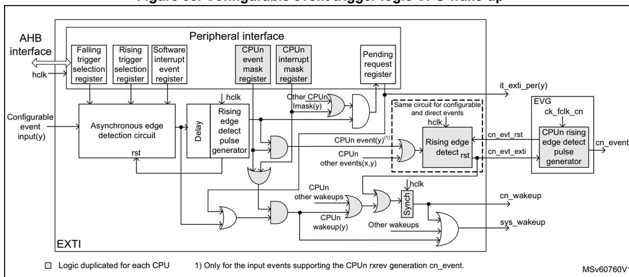
□ Logic duplicated for each CPU 1) Only for the input events supporting the CPU rxev generation cn_event. MSV60760V1
The software interrupt event register allows configurable events to be triggered by software, writing the corresponding register bit, irrespective of the edge selection setting.
The rising and falling edges selection registers allow the configurable event active trigger edge (or both edges) to be enabled.
The CPU has its dedicated interrupt mask and event mask registers. The enabled event allows the generation of an event on the CPU. All events for a CPU are ORed together into a single CPU event signal. The event pending register (EXTI_PR) is not set for an unmasked CPU event.
The configurable events have unique interrupt pending request registers, shared by the CPU. The pending register is only set for an unmasked interrupt. Each configurable event provides a common interrupt to the CPU. The configurable event interrupts need to be acknowledged by software in the EXTI_PR register.
When a CPU interrupt or CPU event is enabled, the asynchronous edge detection circuit is reset by the clocked delay and rising edge detect pulse generator. This guarantees that the EXTI hclk clock is woken up before the asynchronous edge detection circuit is reset.
Note: A detected configurable event interrupt pending request may be cleared by the CPU. The system is not able to enter into low-power modes as long as an interrupt pending request is active.
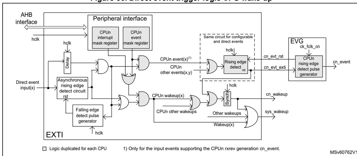
16.4.2 EXTI direct event input wake-up
The extended interrupt/event block diagram for direct events is shown in Figure 56. The direct events allow the wake-up of the system and of the CPU from Sleep and Stop modes.
The direct events do not have an associated EXTI interrupt. The EXTI only wakes up the system and CPU sub-system clocks and may generate a CPU wake-up event. The peripheral synchronous interrupt associated with the direct wake-up event, wake up the CPU. The EXTI direct event is able to generate a CPU event. This CPU event wakes up the CPU.
The CPU event may occur before the associated peripheral interrupt flag is set.
Figure 56. Direct event trigger logic CPU wake-up
16.5 EXTI functional behavior
The direct event inputs are enabled in the respective peripheral generating the wake-up event. The configurable events are enabled by enabling at least one of the trigger edges.
Once an event input is enabled, the generation of a CPU wake-up is conditioned by the CPU interrupt mask and the CPU event mask.
Table 95. Masking functionality
| CPU interrupt enable EXTI_CnIMRm.IMb | CPU event enable EXTI_CnEMRm.EMb | Configurable event inputs EXTI_PRm.PIFb | it_exti_per(y) (1) | CPU event | CPU wake-up |
|---|---|---|---|---|---|
| 0 | 0 | No | Masked | Masked | Masked |
| 1 | No | Masked | Yes | Yes |
Table 95. Masking functionality (continued)
| CPU interrupt enable EXTI_CnIMRm.IMb | CPU event enable EXTI_CnEMRm.EMb | Configurable event inputs EXTI_PRm.PIFb | it_exti_per(y) (1) | CPU n event | CPU n wake-up |
|---|---|---|---|---|---|
| 1 | 0 | Status latched | Yes | Masked | Yes (2) |
| 1 | Status latched | Yes | Yes | Yes |
- 1. The single it_exti_per(y) interrupt goes to both CPUs. If no interrupt is required for the CPU n, the it_exti_per(y) interrupt must be masked in the CPU n NVIC.
- 2. Only if the CPU interrupt is enabled in EXTI_CnIMRm.IMb.
For configurable event inputs, when the enabled edges occur on the event input, an event request is generated. When the associated it_exti_per(y) interrupt is unmasked, the corresponding pending bit in EXTI_PR is set, the CPU sub-system wakes up and the CPU interrupt signal is activated. The EXTI_PR pending bit must be set to 1 by software. This clears the it_exti_per(y) interrupt.
For direct event inputs, when enabled in the associated peripheral, an event request is generated on the rising edge only. There is no corresponding CPU pending bit in the EXTI. When the associated direct event is unmasked in EXTI_IM, the corresponding CPU sub-system wakes up. The CPU is woken up (interrupted) by the peripheral synchronous interrupt.
The CPU event must be unmasked in EXTI_EMR to generate an event. When the enabled edges occur on the event input, a CPU event pulse is generated. There is no event pending bit.
For the configurable event inputs, an event request can be generated by software, setting to 1 the corresponding bit in the interrupt/event register EXTI_SWIER. This allows the generation of a rising edge on the event. The edge event pending bit must be set in EXTI_PR, irrespective of the setting in EXTI_RTSR.
16.6 EXTI registers
The EXTI register map is divided in sections listed in the table below.
Table 96. EXTI register map sections
| Address | Description |
|---|---|
| 0x000 - 0x01C | General configurable event [31:0] configuration |
| 0x020 - 0x03C | General configurable event [63:32] configuration |
| 0x080 - 0x0BC | CPU1 input event configuration |
| 0x0C0 - 0x0FC | CPU2 input event configuration |
All these registers can be accessed with word (32-bit), half-word (16-bit) and byte (8-bit) access.
16.6.1 EXTI rising trigger selection register (EXTI_RTSR1)
Address offset: 0x000
Reset value: 0x0000 0000
Contains only register bits for configurable events.
| 31 | 30 | 29 | 28 | 27 | 26 | 25 | 24 | 23 | 22 | 21 | 20 | 19 | 18 | 17 | 16 |
|---|---|---|---|---|---|---|---|---|---|---|---|---|---|---|---|
| Res. | Res. | Res. | Res. | Res. | Res. | Res. | Res. | Res. | RT22 | RT21 | Res. | Res. | Res. | Res. | RT16 |
| 15 | 14 | 13 | 12 | 11 | 10 | 9 | 8 | 7 | 6 | 5 | 4 | 3 | 2 | 1 | 0 |
| RT15 | RT14 | RT13 | RT12 | RT11 | RT10 | RT9 | RT8 | RT7 | RT6 | RT5 | RT4 | RT3 | RT2 | RT1 | RT0 |
| rw | rw | rw | rw | rw | rw | rw | rw | rw | rw | rw | rw | rw | rw | rw | rw |
Bits 31:23 Reserved, must be kept at reset value.
Bit 22 RT22 : rising trigger event configuration bit of configurable event input 22
0: Rising trigger disabled (for event and interrupt) for input line
1: Rising trigger enabled (for event and interrupt) for input line
Note: The configurable event inputs are edge triggered. No glitch must be generated on these inputs. If a rising edge on the configurable event input occurs while writing to the register, the associated pending bit is not set.
Rising and falling edge triggers can be set for the same configurable event input. In this case, both edges generate a trigger.
Bit 21 RT21 : rising trigger event configuration bit of configurable event input 21
Bits 20:17 Reserved, must be kept at reset value.
Bit 16 RT16 : rising trigger event configuration bit of configurable event input 16
Bit 15 RT15 : rising trigger event configuration bit of configurable event input 15
Bit 14 RT14 : rising trigger event configuration bit of configurable event input 14
Bit 13 RT13 : rising trigger event configuration bit of configurable event input 13
Bit 12 RT12 : rising trigger event configuration bit of configurable event input 12
Bit 11 RT11 : rising trigger event configuration bit of configurable event input 11
Bit 10 RT10 : rising trigger event configuration bit of configurable event input 10
Bit 9 RT9 : rising trigger event configuration bit of configurable event input 9
Bit 8 RT8 : rising trigger event configuration bit of configurable event input 8
Bit 7 RT7 : rising trigger event configuration bit of configurable event input 7
Bit 6 RT6 : rising trigger event configuration bit of configurable event input 6
Bit 5 RT5 : rising trigger event configuration bit of configurable event input 5
Bit 4 RT4 : rising trigger event configuration bit of configurable event input 4
Bit 3 RT3 : rising trigger event configuration bit of configurable event input 3
Bit 2 RT2 : rising trigger event configuration bit of configurable event input 2
Bit 1 RT1 : rising trigger event configuration bit of configurable event input 1
Bit 0 RT0 : rising trigger event configuration bit of configurable event input 0
16.6.2 EXTI falling trigger selection register (EXTI_FTSR1)
Address offset: 0x004
Reset value: 0x0000 0000
Contains only register bits for configurable events.
| 31 | 30 | 29 | 28 | 27 | 26 | 25 | 24 | 23 | 22 | 21 | 20 | 19 | 18 | 17 | 16 |
|---|---|---|---|---|---|---|---|---|---|---|---|---|---|---|---|
| Res. | Res. | Res. | Res. | Res. | Res. | Res. | Res. | Res. | FT22 | FT21 | Res. | Res. | Res. | Res. | FT16 |
| 15 | 14 | 13 | 12 | 11 | 10 | 9 | 8 | 7 | 6 | 5 | 4 | 3 | 2 | 1 | 0 |
| FT15 | FT14 | FT13 | FT12 | FT11 | FT10 | FT9 | FT8 | FT7 | FT6 | FT5 | FT4 | FT3 | FT2 | FT1 | FT0 |
| rw | rw | rw | rw | rw | rw | rw | rw | rw | rw | rw | rw | rw | rw | rw | rw |
Bits 31:23 Reserved, must be kept at reset value.
Bit 22 FT22 : falling trigger event configuration bit of configurable event input 22
0: falling trigger disabled (for event and interrupt) for input line
1: falling trigger enabled (for event and interrupt) for input line
Note: The configurable event inputs are edge triggered. No glitch must be generated on these inputs. If a falling edge on the configurable event input occurs while writing to the register, the associated pending bit is not set.
Rising and falling edge triggers can be set for the same configurable event input. In this case, both edges generate a trigger.
Bit 21 FT21 : falling trigger event configuration bit of configurable event input 21
Bits 20:17 Reserved, must be kept at reset value.
Bit 16 FT16 : falling trigger event configuration bit of configurable event input 16
Bit 15 FT15 : falling trigger event configuration bit of configurable event input 15
Bit 14 FT14 : falling trigger event configuration bit of configurable event input 14
Bit 13 FT13 : falling trigger event configuration bit of configurable event input 13
Bit 12 FT12 : falling trigger event configuration bit of configurable event input 12
Bit 11 FT11 : falling trigger event configuration bit of configurable event input 11
Bit 10 FT10 : falling trigger event configuration bit of configurable event input 10
Bit 9 FT9 : falling trigger event configuration bit of configurable event input 9
Bit 8 FT8 : falling trigger event configuration bit of configurable event input 8
Bit 7 FT7 : falling trigger event configuration bit of configurable event input 7
Bit 6 FT6 : falling trigger event configuration bit of configurable event input 6
Bit 5 FT5 : falling trigger event configuration bit of configurable event input 5
Bit 4 FT4 : falling trigger event configuration bit of configurable event input 4
Bit 3 FT3 : falling trigger event configuration bit of configurable event input 3
Bit 2 FT2 : falling trigger event configuration bit of configurable event input 2
Bit 1 FT1 : falling trigger event configuration bit of configurable event input 1
Bit 0 FT0 : falling trigger event configuration bit of configurable event input 0
16.6.3 EXTI software interrupt event register (EXTI_SWIER1)
Address offset: 0x008
Reset value: 0x0000 0000
Contains only register bits for configurable events.
| 31 | 30 | 29 | 28 | 27 | 26 | 25 | 24 | 23 | 22 | 21 | 20 | 19 | 18 | 17 | 16 |
|---|---|---|---|---|---|---|---|---|---|---|---|---|---|---|---|
| Res. | Res. | Res. | Res. | Res. | Res. | Res. | Res. | Res. | SWI22 | SWI21 | Res. | Res. | Res. | Res. | SWI16 |
| 15 | 14 | 13 | 12 | 11 | 10 | 9 | 8 | 7 | 6 | 5 | 4 | 3 | 2 | 1 | 0 |
| SWI15 | SWI14 | SWI13 | SWI12 | SWI11 | SWI10 | SWI9 | SWI8 | SWI7 | SWI6 | SWI5 | SWI4 | SWI3 | SWI2 | SWI1 | SWI0 |
| rw | rw | rw | rw | rw | rw | rw | rw | rw | rw | rw | rw | rw | rw | rw | rw |
Bits 31:23 Reserved, must be kept at reset value.
Bit 22 SWI22 : Software interrupt on line 22
A software interrupt is generated independently from the setting in EXTI_RTSR and EXTI_FTSR. This bit always returns 0 when read.
0: Writing 0 has no effect.
1: Writing 1 to this bit triggers an event on line 22.
This bit is automatically cleared by hardware.
Bit 21 SWI21 : Software interrupt on line 21
Bits 20:17 Reserved, must be kept at reset value.
Bit 16 SWI16 : Software interrupt on line 16
Bit 15 SWI15 : Software interrupt on line 15
Bit 14 SWI14 : Software interrupt on line 14
Bit 13 SWI13 : Software interrupt on line 13
Bit 12 SWI12 : Software interrupt on line 12
Bit 11 SWI11 : Software interrupt on line 11
Bit 10 SWI10 : Software interrupt on line 10
Bit 9 SWI9 : Software interrupt on line 9
Bit 8 SWI8 : Software interrupt on line 8
Bit 7 SWI7 : Software interrupt on line 7
Bit 6 SWI6 : Software interrupt on line 6
Bit 5 SWI5 : Software interrupt on line 5
Bit 4 SWI4 : Software interrupt on line 4
Bit 3 SWI3 : Software interrupt on line 3
Bit 2 SWI2 : Software interrupt on line 2
Bit 1 SWI1 : Software interrupt on line 1
Bit 0 SWI0 : Software interrupt on line 0
16.6.4 EXTI pending register (EXTI_PR1)
Address offset: 0x00C
Reset value: 0x0000 0000
Contains only register bits for configurable events.
| 31 | 30 | 29 | 28 | 27 | 26 | 25 | 24 | 23 | 22 | 21 | 20 | 19 | 18 | 17 | 16 |
|---|---|---|---|---|---|---|---|---|---|---|---|---|---|---|---|
| Res. | Res. | Res. | Res. | Res. | Res. | Res. | Res. | Res. | PIF22 | PIF21 | Res. | Res. | Res. | Res. | PIF16 |
| 15 | 14 | 13 | 12 | 11 | 10 | 9 | 8 | 7 | 6 | 5 | 4 | 3 | 2 | 1 | 0 |
| PIF15 | PIF14 | PIF13 | PIF12 | PIF11 | PIF10 | PIF9 | PIF8 | PIF7 | PIF6 | PIF5 | PIF4 | PIF3 | PIF2 | PIF1 | PIF0 |
| rw | rw | rw | rw | rw | rw | rw | rw | rw | rw | rw | rw | rw | rw | rw | rw |
Bits 31:23 Reserved, must be kept at reset value.
Bit 22 PIF22 : pending bit on event input 22
These bits are set when the selected edge event or an EXTI_SWIER software trigger arrives on the configurable event line. This bit is cleared by writing 1 to it.
0: No trigger request occurred.
1: Trigger request occurred.
Bit 21 PIF21 : pending bit on event input 21
Bits 20:17 Reserved, must be kept at reset value.
Bit 16 PIF16 : pending bit on event input 16
Bit 15 PIF15 : pending bit on event input 15
Bit 14 PIF14 : pending bit on event input 14
Bit 13 PIF13 : pending bit on event input 13
Bit 12 PIF12 : pending bit on event input 12
Bit 11 PIF11 : pending bit on event input 11
Bit 10 PIF10 : pending bit on event input 10
Bit 9 PIF9 : pending bit on event input 9
Bit 8 PIF8 : pending bit on event input 8
Bit 7 PIF7 : pending bit on event input 7
Bit 6 PIF6 : pending bit on event input 6
Bit 5 PIF5 : pending bit on event input 5
Bit 4 PIF4 : pending bit on event input 4
Bit 3 PIF3 : pending bit on event input 3
Bit 2 PIF2 : pending bit on event input 2
Bit 1 PIF1 : pending bit on event input 1
Bit 0 PIF0 : pending bit on event input 0
16.6.5 EXTI rising trigger selection register (EXTI_RTSR2)
Address offset: 0x020
Reset value: 0x0000 0000
Contains only register bits for configurable events.
| 31 | 30 | 29 | 28 | 27 | 26 | 25 | 24 | 23 | 22 | 21 | 20 | 19 | 18 | 17 | 16 |
|---|---|---|---|---|---|---|---|---|---|---|---|---|---|---|---|
| Res. | Res. | Res. | Res. | Res. | Res. | Res. | Res. | Res. | Res. | Res. | Res. | Res. | Res. | Res. | Res. |
| 15 | 14 | 13 | 12 | 11 | 10 | 9 | 8 | 7 | 6 | 5 | 4 | 3 | 2 | 1 | 0 |
| Res. | Res. | RT45 | Res. | Res. | Res. | RT41 | RT40 | Res. | Res. | Res. | Res. | Res. | RT34 | Res. | Res. |
| rw | rw | rw | rw |
Bits 31:14 Reserved, must be kept at reset value.
Bit 13 RT45 : rising trigger event configuration bit of configurable event input 45
0: Rising trigger disabled (for event and interrupt) for input line
1: Rising trigger enabled (for event and interrupt) for input line
Note: The configurable event inputs are edge triggered. No glitch must be generated on these inputs. If a rising edge on the configurable event input occurs while writing to the register, the associated pending bit is not set.
Rising and falling edge triggers can be set for the same configurable event input. In this case, both edges generate a trigger.
Bits 12:10 Reserved, must be kept at reset value.
Bit 9 RT41 : rising trigger event configuration bit of configurable event input 41
Bit 8 RT40 : rising trigger event configuration bit of configurable event input 40
Bits 7:3 Reserved, must be kept at reset value.
Bit 2 RT34 : rising trigger event configuration bit of configurable event input 34
Bits 1:0 Reserved, must be kept at reset value.
16.6.6 EXTI falling trigger selection register (EXTI_FTSR2)
Address offset: 0x024
Reset value: 0x0000 0000
Contains only register bits for configurable events.
| 31 | 30 | 29 | 28 | 27 | 26 | 25 | 24 | 23 | 22 | 21 | 20 | 19 | 18 | 17 | 16 |
|---|---|---|---|---|---|---|---|---|---|---|---|---|---|---|---|
| Res. | Res. | Res. | Res. | Res. | Res. | Res. | Res. | Res. | Res. | Res. | Res. | Res. | Res. | Res. | Res. |
| 15 | 14 | 13 | 12 | 11 | 10 | 9 | 8 | 7 | 6 | 5 | 4 | 3 | 2 | 1 | 0 |
| Res. | Res. | FT45 | Res. | Res. | Res. | FT41 | FT40 | Res. | Res. | Res. | Res. | Res. | FT34 | Res. | Res. |
| rw | rw | rw | rw |
Bits 31:14 Reserved, must be kept at reset value.
Bit 13 FT45 : falling trigger event configuration bit of configurable event input 45
0: Falling trigger disabled (for event and interrupt) for input line
1: Falling trigger enabled (for event and interrupt) for input line
Note: The configurable event inputs are edge triggered. No glitch must be generated on these inputs. If a falling edge on the configurable event input occurs while writing to the register, the associated pending bit is not set.
Rising and falling edge triggers can be set for the same configurable event input. In this case, both edges generate a trigger.
Bits 12:10 Reserved, must be kept at reset value.
Bit 9 FT41 : falling trigger event configuration bit of configurable event input 41
Bit 8 FT40 : falling trigger event configuration bit of configurable event input 40
Bits 7:3 Reserved, must be kept at reset value.
Bit 2 FT34 : falling trigger event configuration bit of configurable event input 34
Bits 1:0 Reserved, must be kept at reset value.
16.6.7 EXTI software interrupt event register (EXTI_SWIER2)
Address offset: 0x028
Reset value: 0x0000 0000
Contains only register bits for configurable events.
| 31 | 30 | 29 | 28 | 27 | 26 | 25 | 24 | 23 | 22 | 21 | 20 | 19 | 18 | 17 | 16 |
|---|---|---|---|---|---|---|---|---|---|---|---|---|---|---|---|
| Res. | Res. | Res. | Res. | Res. | Res. | Res. | Res. | Res. | Res. | Res. | Res. | Res. | Res. | Res. | Res. |
| 15 | 14 | 13 | 12 | 11 | 10 | 9 | 8 | 7 | 6 | 5 | 4 | 3 | 2 | 1 | 0 |
| Res. | Res. | SWI45 | Res. | Res. | Res. | SWI41 | SWI40 | Res. | Res. | Res. | Res. | Res. | SWI34 | Res. | Res. |
| rw | rw | rw | rw |
Bits 31:14 Reserved, must be kept at reset value.
Bit 13 SWI45 : software interrupt on event 45
A software interrupt is generated independently from the setting in EXTI_RTSR and EXTI_FTSR. This bit always returns 0 when read.
0: Writing 0 has no effect.
1: Writing 1 to this bit triggers an event on line 45.
This bit is automatically cleared by hardware.
Bits 12:10 Reserved, must be kept at reset value.
Bit 9 SWI41 : software interrupt on event 41
Bit 8 SWI40 : software interrupt on event 40
Bits 7:3 Reserved, must be kept at reset value.
Bit 2 SWI34 : software interrupt on event 34
Bits 1:0 Reserved, must be kept at reset value.
16.6.8 EXTI pending register (EXTI_PR2)
Address offset: 0x02C
Reset value: 0x0000 0000
Contains only register bits for configurable events.
| 31 | 30 | 29 | 28 | 27 | 26 | 25 | 24 | 23 | 22 | 21 | 20 | 19 | 18 | 17 | 16 |
|---|---|---|---|---|---|---|---|---|---|---|---|---|---|---|---|
| Res. | Res. | Res. | Res. | Res. | Res. | Res. | Res. | Res. | Res. | Res. | Res. | Res. | Res. | Res. | Res. |
| 15 | 14 | 13 | 12 | 11 | 10 | 9 | 8 | 7 | 6 | 5 | 4 | 3 | 2 | 1 | 0 |
| Res. | Res. | PIF45 | Res. | Res. | Res. | PIF41 | PIF40 | Res. | Res. | Res. | Res. | Res. | PIF34 | Res. | Res. |
| rw | rw | rw | rw |
Bits 31:14 Reserved, must be kept at reset value.
Bit 13 PIF45 : pending bit on event input 45
These bits are set when the selected edge event or an EXTI_SWIER software trigger arrives on the configurable event line. This bit is cleared by writing 1 to it.
0: No trigger request occurred.
1: Trigger request occurred.
Bits 12:10 Reserved, must be kept at reset value.
Bit 9 PIF41 : pending bit on event input 41
Bit 8 PIF40 : pending bit on event input 40
Bits 7:3 Reserved, must be kept at reset value.
Bit 2 PIF34 : pending bit on event input 34
Bits 1:0 Reserved, must be kept at reset value.
16.6.9 EXTI interrupt mask register (EXTI_CnIMR1)
Address offset: Block 1: 0x080
Address offset: Block 2: 0x0C0
Reset value: 0x0000 0000
| 31 | 30 | 29 | 28 | 27 | 26 | 25 | 24 | 23 | 22 | 21 | 20 | 19 | 18 | 17 | 16 |
|---|---|---|---|---|---|---|---|---|---|---|---|---|---|---|---|
| IM[31:16] | |||||||||||||||
| rw | rw | rw | rw | rw | rw | rw | rw | rw | rw | rw | rw | rw | rw | rw | rw |
| 15 | 14 | 13 | 12 | 11 | 10 | 9 | 8 | 7 | 6 | 5 | 4 | 3 | 2 | 1 | 0 |
| IM[15:0] | |||||||||||||||
| rw | rw | rw | rw | rw | rw | rw | rw | rw | rw | rw | rw | rw | rw | rw | rw |
Bits 31:0 IM[31:0] : Wake-up with interrupt mask on event input x (x= 31 to 0)
For each bit of this field:
0: Wake-up with interrupt request from line x is masked.
1: Wake-up with Interrupt request from line x is unmasked.
16.6.10 EXTI event mask register (EXTI_CnEMR1)
Address offset: Block 1: 0x084
Address offset: Block 2: 0x0C4
Reset value: 0x0000 0000
| 31 | 30 | 29 | 28 | 27 | 26 | 25 | 24 | 23 | 22 | 21 | 20 | 19 | 18 | 17 | 16 |
|---|---|---|---|---|---|---|---|---|---|---|---|---|---|---|---|
| Res. | Res. | Res. | Res. | Res. | Res. | Res. | Res. | Res. | EM22 | EM21 | EM20 | EM19 | EM18 | EM17 | Res. |
| 15 | 14 | 13 | 12 | 11 | 10 | 9 | 8 | 7 | 6 | 5 | 4 | 3 | 2 | 1 | 0 |
| EM15 | EM14 | EM13 | EM12 | EM11 | EM10 | EM9 | EM8 | EM7 | EM6 | EM5 | EM4 | EM3 | EM2 | EM1 | EM0 |
| rw | rw | rw | rw | rw | rw | rw | rw | rw | rw | rw | rw | rw | rw | rw | rw |
Bits 31:23 Reserved, must be kept at reset value.
Bit 22 EM22 : Wake-up with event generation mask on event input 22
0: Event request from line 22 is masked.
1: Event request from line 22 is unmasked.
Bit 21 EM21 : Wake-up with event generation mask on event input 21
Bit 20 EM20 : Wake-up with event generation mask on event input 20
Bit 19 EM19 : Wake-up with event generation mask on event input 19
Bit 18 EM18 : Wake-up with event generation mask on event input 18
Bit 17 EM17 : Wake-up with event generation mask on event input 17
Bit 16 Reserved, must be kept at reset value.
Bit 15 EM15 : Wake-up with event generation mask on event input 15
Bit 14 EM14 : Wake-up with event generation mask on event input 14
Bit 13 EM13 : Wake-up with event generation mask on event input 13
Bit 12 EM12 : Wake-up with event generation mask on event input 12
Bit 11 EM11 : Wake-up with event generation mask on event input 11
Bit 10 EM10 : Wake-up with event generation mask on event input 10
Bit 9 EM9 : Wake-up with event generation mask on event input 9
Bit 8 EM8 : Wake-up with event generation mask on event input 8
Bit 7 EM7 : Wake-up with event generation mask on event input 7
Bit 6 EM6 : Wake-up with event generation mask on event input 6
Bit 5 EM5 : Wake-up with event generation mask on event input 5
Bit 4 EM4 : Wake-up with event generation mask on event input 4
Bit 3 EM3 : Wake-up with event generation mask on event input 3
Bit 2 EM2 : Wake-up with event generation mask on event input 2
Bit 1 EM1 : Wake-up with event generation mask on event input 1
Bit 0 EM0 : Wake-up with event generation mask on event input 0
16.6.11 EXTI interrupt mask register (EXTI_CnIMR2)
Address offset: Block 1: 0x090
Address offset: Block 2: 0x0D0
Reset value: 0x0000 0000
| 31 | 30 | 29 | 28 | 27 | 26 | 25 | 24 | 23 | 22 | 21 | 20 | 19 | 18 | 17 | 16 |
|---|---|---|---|---|---|---|---|---|---|---|---|---|---|---|---|
| Res. | Res. | Res. | Res. | Res. | Res. | Res. | Res. | Res. | Res. | Res. | Res. | Res. | Res. | Res. | Res. |
| 15 | 14 | 13 | 12 | 11 | 10 | 9 | 8 | 7 | 6 | 5 | 4 | 3 | 2 | 1 | 0 |
| Res. | IM46 | IM45 | IM44 | IM43 | IM42 | IM41 | IM40 | IM39 | IM38 | IM37 | IM36 | Res. | IM34 | Res. | Res. |
| rw | rw | rw | rw | rw | rw | rw | rw | rw | rw | rw | rw |
Bits 31:15 Reserved, must be kept at reset value.
Bit 14 IM46 : Wake-up with interrupt mask on event input 46
0: Wake-up with interrupt request from line 46 is masked.
1: Wake-up with interrupt request from line 46 is unmasked.
Bit 13 IM45 : Wake-up with interrupt mask on event input 45
Bit 12 IM44 : Wake-up with interrupt mask on event input 44
Bit 11 IM43 : Wake-up with interrupt mask on event input 43
Bit 10 IM42 : Wake-up with interrupt mask on event input 42
Bit 9 IM41 : Wake-up with interrupt mask on event input 41
Bit 8 IM40 : Wake-up with interrupt mask on event input 40
Bit 7 IM39 : Wake-up with interrupt mask on event input 39
Bit 6 IM38 : Wake-up with interrupt mask on event input 38
Bit 5 IM37 : Wake-up with interrupt mask on event input 37
Bit 4 IM36 : Wake-up with interrupt mask on event input 36
Bit 3 Reserved, must be kept at reset value.
Bit 2 IM34 : Wake-up with interrupt mask on event input 34
Bits 1:0 Reserved, must be kept at reset value.
16.6.12 EXTI event mask register (EXTI_CnEMR2)
Address offset: Block 1: 0x094
Address offset: Block 2: 0x0D4
Reset value: 0x0000 0000
| 31 | 30 | 29 | 28 | 27 | 26 | 25 | 24 | 23 | 22 | 21 | 20 | 19 | 18 | 17 | 16 |
|---|---|---|---|---|---|---|---|---|---|---|---|---|---|---|---|
| Res. | Res. | Res. | Res. | Res. | Res. | Res. | Res. | Res. | Res. | Res. | Res. | Res. | Res. | Res. | Res. |
| 15 | 14 | 13 | 12 | 11 | 10 | 9 | 8 | 7 | 6 | 5 | 4 | 3 | 2 | 1 | 0 |
| Res. | Res. | Res. | Res. | Res. | Res. | EM41 | EM40 | Res. | Res. | Res. | Res. | Res. | Res. | Res. | Res. |
| rw | rw |
Bits 31:10 Reserved, must be kept at reset value.
Bit 9 EM41 : Wake-up with event generation mask on event input 41
0: Event request from line 41 is masked.
1: Event request from line 41 is unmasked.
Bit 8 EM40 : Wake-up with event generation mask on event input 40
Bits 7:0 Reserved, must be kept at reset value.
16.6.13 EXTI register map
Table 97. EXTI register map and reset values
| Offset | Register name | 31 | 30 | 29 | 28 | 27 | 26 | 25 | 24 | 23 | 22 | 21 | 20 | 19 | 18 | 17 | 16 | 15 | 14 | 13 | 12 | 11 | 10 | 9 | 8 | 7 | 6 | 5 | 4 | 3 | 2 | 1 | 0 | |
|---|---|---|---|---|---|---|---|---|---|---|---|---|---|---|---|---|---|---|---|---|---|---|---|---|---|---|---|---|---|---|---|---|---|---|
| 0x000 | EXTI_RTSR1 | Res. | Res. | Res. | Res. | Res. | Res. | Res. | Res. | Res. | RT22 | RT21 | Res. | Res. | Res. | Res. | RT16 | RT15 | RT14 | RT13 | RT12 | RT11 | RT10 | RT9 | RT8 | RT7 | RT6 | RT5 | RT4 | RT3 | RT2 | RT1 | RT0 | |
| Reset value | 0 | 0 | 0 | 0 | 0 | 0 | 0 | 0 | 0 | 0 | 0 | 0 | 0 | 0 | 0 | 0 | 0 | 0 | 0 | |||||||||||||||
| 0x004 | EXTI_FTSR1 | Res. | Res. | Res. | Res. | Res. | Res. | Res. | Res. | Res. | FT22 | FT21 | Res. | Res. | Res. | Res. | FT16 | FT15 | FT14 | FT13 | FT12 | FT11 | FT10 | FT9 | FT8 | FT7 | FT6 | FT5 | FT4 | FT3 | FT2 | FT1 | FT0 | |
| Reset value | 0 | 0 | 0 | 0 | 0 | 0 | 0 | 0 | 0 | 0 | 0 | 0 | 0 | 0 | 0 | 0 | 0 | 0 | 0 | |||||||||||||||
| 0x008 | EXTI_SWIER1 | Res. | Res. | Res. | Res. | Res. | Res. | Res. | Res. | Res. | SWI22 | SWI21 | Res. | Res. | Res. | Res. | SWI16 | SWI15 | SWI14 | SWI13 | SWI12 | SWI11 | SWI10 | SWI9 | SWI8 | SWI7 | SWI6 | SWI5 | SWI4 | SWI3 | SWI2 | SWI1 | SWI0 | |
| Reset value | 0 | 0 | 0 | 0 | 0 | 0 | 0 | 0 | 0 | 0 | 0 | 0 | 0 | 0 | 0 | 0 | 0 | 0 | 0 | |||||||||||||||
| 0x00C | EXTI_PR1 | Res. | Res. | Res. | Res. | Res. | Res. | Res. | Res. | Res. | PIF22 | PIF21 | Res. | Res. | Res. | Res. | PIF16 | PIF15 | PIF14 | PIF13 | PIF12 | PIF11 | PIF10 | PIF9 | PIF8 | PIF7 | PIF6 | PIF5 | PIF4 | PIF3 | PIF2 | PIF1 | PIF0 | |
| Reset value | 0 | 0 | 0 | 0 | 0 | 0 | 0 | 0 | 0 | 0 | 0 | 0 | 0 | 0 | 0 | 0 | 0 | 0 | 0 | |||||||||||||||
| 0x010- 0x01C | Reserved | Reserved. | ||||||||||||||||||||||||||||||||
| 0x020 | EXTI_RTSR2 | Res. | Res. | Res. | Res. | Res. | Res. | Res. | Res. | Res. | Res. | Res. | Res. | Res. | Res. | Res. | Res. | Res. | Res. | RT45 | Res. | Res. | Res. | RT41 | RT40 | Res. | Res. | Res. | Res. | Res. | Res. | RT34 | Res. | Res. |
| Reset value | 0 | 0 | 0 | 0 | ||||||||||||||||||||||||||||||
| 0x024 | EXTI_FTSR2 | Res. | Res. | Res. | Res. | Res. | Res. | Res. | Res. | Res. | Res. | Res. | Res. | Res. | Res. | Res. | Res. | Res. | Res. | FT45 | Res. | Res. | Res. | FT41 | FT40 | Res. | Res. | Res. | Res. | Res. | Res. | FT34 | Res. | Res. |
| Reset value | 0 | 0 | 0 | 0 | ||||||||||||||||||||||||||||||
| 0x028 | EXTI_SWIER2 | Res. | Res. | Res. | Res. | Res. | Res. | Res. | Res. | Res. | Res. | Res. | Res. | Res. | Res. | Res. | Res. | Res. | Res. | SWI45 | Res. | Res. | Res. | SWI41 | SWI40 | Res. | Res. | Res. | Res. | Res. | Res. | SWI34 | Res. | Res. |
| Reset value | 0 | 0 | 0 | 0 | ||||||||||||||||||||||||||||||
| 0x02C | EXTI_PR2 | Res. | Res. | Res. | Res. | Res. | Res. | Res. | Res. | Res. | Res. | Res. | Res. | Res. | Res. | Res. | Res. | Res. | Res. | PIF45 | Res. | Res. | Res. | PIF41 | PIF40 | Res. | Res. | Res. | Res. | Res. | Res. | PIF34 | Res. | Res. |
| Reset value | 0 | 0 | 0 | 0 | ||||||||||||||||||||||||||||||
| 0x030- 0x07C | Reserved | Reserved. | ||||||||||||||||||||||||||||||||
| 0x080 | EXTI_C1IMR1 | IM31 | IM30 | IM29 | IM28 | IM27 | IM26 | IM25 | IM24 | IM23 | IM22 | IM21 | IM20 | IM19 | IM18 | IM17 | IM16 | IM15 | IM14 | IM13 | IM12 | IM11 | IM10 | IM9 | IM8 | IM7 | IM6 | IM5 | IM4 | IM3 | IM2 | IM1 | IM0 | |
| Reset value | 0 | 0 | 0 | 0 | 0 | 0 | 0 | 0 | 0 | 0 | 0 | 0 | 0 | 0 | 0 | 0 | 0 | 0 | 0 | 0 | 0 | 0 | 0 | 0 | 0 | 0 | 0 | 0 | 0 | 0 | 0 | 0 | ||
| 0x084 | EXTI_C1EMR1 | Res. | Res. | Res. | Res. | Res. | Res. | Res. | Res. | Res. | EM22 | EM21 | EM20 | EM19 | EM18 | EM17 | Res. | EM15 | EM14 | EM13 | EM12 | EM11 | EM10 | EM9 | EM8 | EM7 | EM6 | EM5 | EM4 | EM3 | EM2 | EM1 | EM0 | |
| Reset value | 0 | 0 | 0 | 0 | 0 | 0 | 0 | 0 | 0 | 0 | 0 | 0 | 0 | 0 | 0 | 0 | 0 | 0 | 0 | 0 | 0 | 0 | ||||||||||||
| 0x08C | Reserved | Reserved. | ||||||||||||||||||||||||||||||||
| 0x090 | EXTI_C1IMR2 | Res. | Res. | Res. | Res. | Res. | Res. | Res. | Res. | Res. | Res. | Res. | Res. | Res. | Res. | Res. | Res. | Res. | Res. | IM46 | IM45 | IM44 | IM43 | IM42 | IM41 | IM40 | IM39 | IM38 | IM37 | IM36 | Res. | IM34 | Res. | Res. |
| Reset value | 0 | 0 | 0 | 0 | 0 | 0 | 0 | 0 | 0 | 0 | 0 | 0 | ||||||||||||||||||||||
| 0x094 | EXTI_C1EMR2 | Res. | Res. | Res. | Res. | Res. | Res. | Res. | Res. | Res. | Res. | Res. | Res. | Res. | Res. | Res. | Res. | Res. | Res. | Res. | Res. | Res. | Res. | EM41 | EM40 | Res. | Res. | Res. | Res. | Res. | Res. | Res. | Res. | Res. |
| Reset value | 0 | 0 | ||||||||||||||||||||||||||||||||
| 0x098- 0x0BF | Reserved | Reserved. | ||||||||||||||||||||||||||||||||
Table 97. EXTI register map and reset values (continued)
| Offset | Register name | 31 | 30 | 29 | 28 | 27 | 26 | 25 | 24 | 23 | 22 | 21 | 20 | 19 | 18 | 17 | 16 | 15 | 14 | 13 | 12 | 11 | 10 | 9 | 8 | 7 | 6 | 5 | 4 | 3 | 2 | 1 | 0 |
|---|---|---|---|---|---|---|---|---|---|---|---|---|---|---|---|---|---|---|---|---|---|---|---|---|---|---|---|---|---|---|---|---|---|
| 0x0C0 | EXTI_C2IMR1 | IM31 | IM30 | IM29 | IM28 | IM27 | IM26 | IM25 | IM24 | IM23 | IM22 | IM21 | IM20 | IM19 | IM18 | IM17 | IM16 | IM15 | IM14 | IM13 | IM12 | IM11 | IM10 | IM9 | IM8 | IM7 | IM6 | IM5 | IM4 | IM3 | IM2 | IM1 | IM0 |
| Reset value | 0 | 0 | 0 | 0 | 0 | 0 | 0 | 0 | 0 | 0 | 0 | 0 | 0 | 0 | 0 | 0 | 0 | 0 | 0 | 0 | 0 | 0 | 0 | 0 | 0 | 0 | 0 | 0 | 0 | 0 | 0 | 0 | |
| 0x0C4 | EXTI_C2EMR1 | Res. | Res. | Res. | Res. | Res. | Res. | Res. | Res. | Res. | EM22 | EM21 | EM20 | EM19 | EM18 | EM17 | Res. | EM15 | EM14 | EM13 | EM12 | EM11 | EM10 | EM9 | EM8 | EM7 | EM6 | EM5 | EM4 | EM3 | EM2 | EM1 | EM0 |
| Reset value | 0 | 0 | 0 | 0 | 0 | 0 | 0 | 0 | 0 | 0 | 0 | 0 | 0 | 0 | 0 | 0 | 0 | 0 | 0 | 0 | 0 | 0 | |||||||||||
| 0x0C8 | Reserved | Reserved | |||||||||||||||||||||||||||||||
| 0x0D0 | EXTI_C2IMR2 | Res. | Res. | Res. | Res. | Res. | Res. | Res. | Res. | Res. | Res. | Res. | Res. | Res. | Res. | Res. | Res. | Res. | IM46 | IM45 | IM44 | IM46 | IM42 | IM41 | IM40 | IM39 | IM38 | IM37 | IM36 | Res. | Res. | Res. | Res. |
| Reset value | 0 | 0 | 0 | 0 | 0 | 0 | 0 | 0 | 0 | 0 | 0 | ||||||||||||||||||||||
| 0x0D4 | EXTI_C2EMR2 | Res. | Res. | Res. | Res. | Res. | Res. | Res. | Res. | Res. | Res. | Res. | Res. | Res. | Res. | Res. | Res. | Res. | Res. | Res. | Res. | Res. | Res. | EM41 | EM40 | Res. | Res. | Res. | Res. | Res. | Res. | Res. | Res. |
| Reset value | 0 | 0 | |||||||||||||||||||||||||||||||
Refer to Section 2.6 for the register boundary addresses.