9. Inter-processor communication controller (IPCC)
9.1 Introduction
The inter-processor communication controller (IPCC) is used for communicating data between two processors.
The IPCC block provides a nonblocking signaling mechanism to post and retrieve communication data in an atomic way. It provides the signaling for twelve channels:
- • six channels in the direction from processor 1 to processor 2
- • six channels in the opposite direction
It is then possible to have two different communication types in each direction.
The IPCC communication data must be located in a common memory, which is not part of the IPCC block.
9.2 IPCC main features
- • Status signaling for the twelve channels
- – Channel occupied/free flag, also used as lock
- • Two interrupt lines per processor
- – One for RX channel occupied (communication data posted by sending processor)
- – One for TX channel free (communication data retrieved by receiving processor)
- • Interrupt masking per channel
- – Channel occupied mask
- – Channel free mask
- • Two channel operation modes
- – Simplex (each channel has its own communication data memory location)
- – Half duplex (a single channel associated to a bidirectional communication data information memory location)
9.3 IPCC functional description
The IPCC communication data is located in a common memory, which is not part of the IPCC block. The address location of the communication data must be known or located in a known common area that, as already stated, is not part of the IPCC block.
For each communication, the IPCC block provides a channel status flag CHnF.
- • When 0, the channel status flag CHnF indicates that the associated IPCC channel is free (the receiving processor has retrieved communication data), and can be accessed by the sending processor.
- • When 1, the channel status flag CHnF indicates that the associated IPCC channel is occupied (the sending processor has posted communication data) and can be accessed by the receiving processor.
The channel operation mode must be known to both processors. A common parameter can be used to indicate the channel transfer mode and must also be located in a known common area. This parameter is not available from the IPCC.
9.3.1 IPCC block diagram
The IPCC (see Figure 36) consists of the following subblocks:
- • Status block, containing the channel status
- • IPCC interface block, providing AHB access to the channel status registers
- • Interrupt interface block, providing control for the interrupts
Figure 36. IPCC block diagram
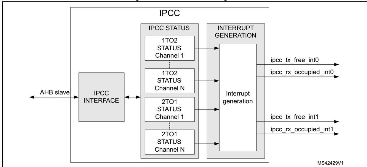
The diagram illustrates the internal architecture of the IPCC. On the left, an 'IPCC INTERFACE' block is connected to an 'AHB slave' bus. This interface connects to the 'IPCC STATUS' block, which contains multiple status registers: '1TO2 STATUS Channel 1', '1TO2 STATUS Channel N', '2TO1 STATUS Channel 1', and '2TO1 STATUS Channel N'. These registers are connected to the 'INTERRUPT GENERATION' block, which contains an 'Interrupt generation' sub-block. The 'INTERRUPT GENERATION' block outputs four interrupt signals: 'ipcc_tx_free_int0', 'ipcc_rx_occupied_int0', 'ipcc_tx_free_int1', and 'ipcc_rx_occupied_int1'. The diagram is labeled with the reference 'MS42429V1' in the bottom right corner.
Table 67. IPCC interface signals
| Signal | Description | |
|---|---|---|
| Name | Type | |
| AHB slave | I/O | AHB register access bus |
| ipcc_tx_free_int1 | O | TX free interrupt to processor 1 |
| ipcc_rx_occupied_int1 | O | RX occupied interrupt to processor 1 |
| ipcc_tx_free_int2 | O | TX free interrupt to processor 2 |
| ipcc_rx_occupied_int2 | O | RX occupied interrupt to processor 2 |
9.3.2 IPCC Simplex channel mode
In Simplex channel mode, a dedicated memory location (used to transfer data in a single direction) is assigned to the communication data. The associated channel N control bits (see Table 68) are used to manage the transfer from the sending to the receiving processor.
Table 68. Bits used for the communication
| Processor | A | B |
|---|---|---|
| SEND A = 1 RECEIVE B = 2 | IPCC_C1CR.TXFIE IPCC_C1MR.CHnFM IPCC_C1SCR.CHnS IPCC_C1TOC2SR.CHnF | IPCC_C2CR.RXOIE IPCC_C2MR.CHnOM IPCC_C2SCR.CHnC |
| SEND A = 2 RECEIVE B = 1 | IPCC_C2CR.TXFIE IPCC_C2MR.CHnFM IPCC_C2SCR.CHnS IPCC_C2TOC1SR.CHnF | IPCC_C1CR.RXOIE IPCC_C1MR.CHnOM IPCC_C1SCR.CHnC |
Once the sending processor has posted the communication data in the memory, it sets the channel status flag CHnF to occupied with CHnS.
Once the receiving processor has retrieved the communication data from the memory, it clears the channel status flag CHnF back to free with CHnC.
Figure 37. IPCC Simplex channel mode transfer timing
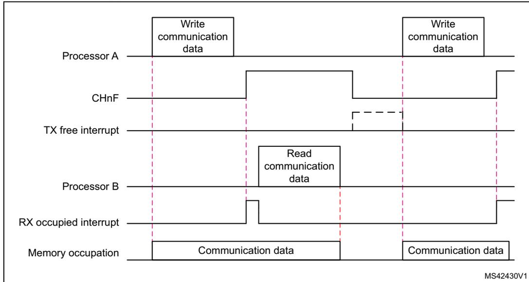
The timing diagram illustrates the interaction between Processor A and Processor B for a simplex channel transfer. The vertical axis lists the components: Processor A, CHnF (Channel Status Flag), TX free interrupt, Processor B, RX occupied interrupt, and Memory occupation. The horizontal axis represents time.
1.
Processor A
: Initiates the transfer by writing communication data to memory.
2.
Memory occupation
: The data is written to a specific memory location, indicated by a block labeled "Communication data".
3.
CHnF
: The flag is set to 'occupied' (high) immediately after the data is written.
4.
RX occupied interrupt
: Processor B detects the occupied flag and generates a short pulse interrupt.
5.
Processor B
: Retrieves the communication data from memory, indicated by a block labeled "Read communication data".
6.
CHnF
: The flag is cleared to 'free' (low) after the data is read.
7.
TX free interrupt
: Processor A detects the free flag and generates a short pulse interrupt (shown with a dashed line indicating it's optional or specific to a configuration).
8.
Processor A
: Can then initiate a new write of communication data.
The diagram shows two instances of this sequence. Vertical dashed lines mark the key synchronization events. A label 'MS42430V1' is present in the bottom right corner.
Figure 38. IPCC Simplex - Send procedure state diagram
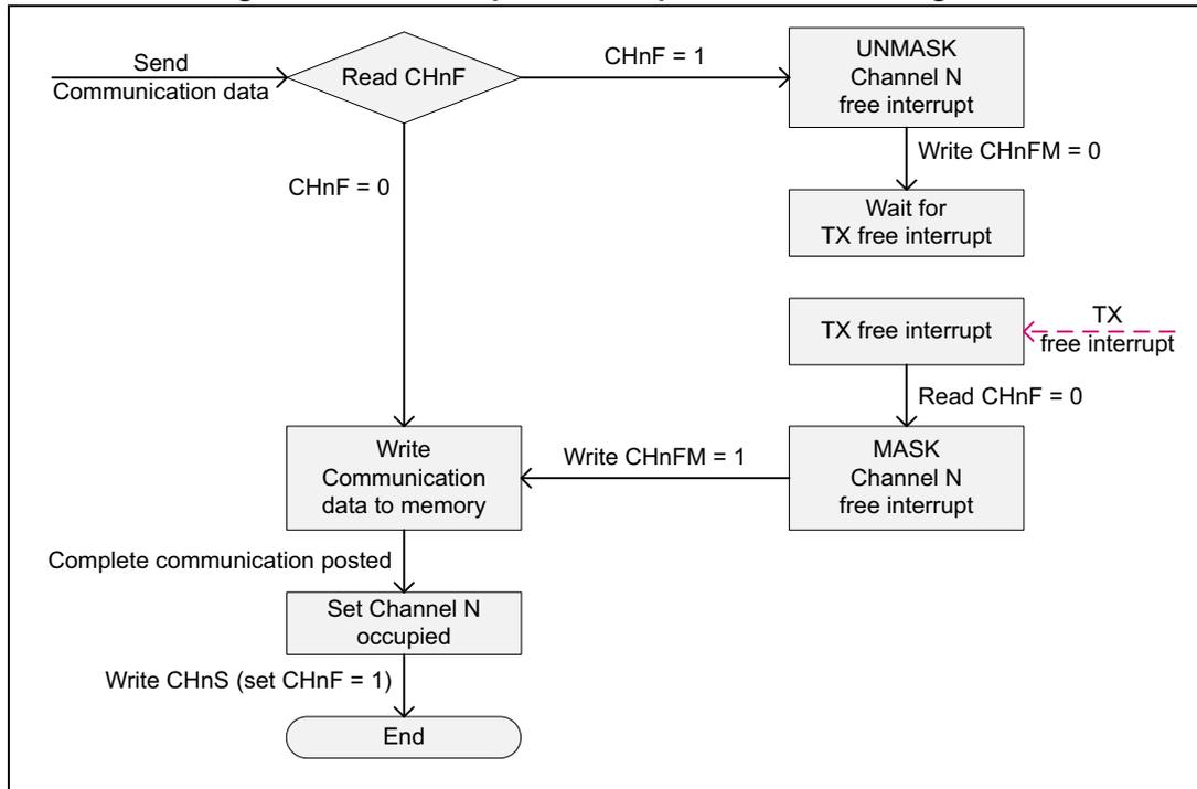
graph TD; Start(( )) -- "Send Communication data" --> ReadCHnF{Read CHnF}; ReadCHnF -- "CHnF = 1" --> UNMASK[UNMASK Channel N free interrupt]; UNMASK -- "Write CHnFM = 0" --> Wait[Wait for TX free interrupt]; Wait --> TXFree[TX free interrupt]; TXFree -- "Read CHnF = 0" --> MASK[MASK Channel N free interrupt]; MASK -- "Write CHnFM = 1" --> WriteData[Write Communication data to memory]; ReadCHnF -- "CHnF = 0" --> WriteData; WriteData -- "Complete communication posted" --> SetOccupied[Set Channel N occupied]; SetOccupied -- "Write CHnS (set CHnF = 1)" --> End([End]);The state diagram illustrates the send procedure for the IPCC Simplex. It begins with the 'Send Communication data' input, leading to a decision point 'Read CHnF'. If 'CHnF = 1', the flow goes to 'UNMASK Channel N free interrupt', then 'Write CHnFM = 0', 'Wait for TX free interrupt', and 'TX free interrupt'. From 'TX free interrupt', a dashed pink arrow labeled 'TX free interrupt' points to the next step 'Read CHnF = 0', which leads to 'MASK Channel N free interrupt'. From 'MASK Channel N free interrupt', the flow goes to 'Write CHnFM = 1', which then leads to 'Write Communication data to memory'. If 'CHnF = 0' at the initial 'Read CHnF' decision, the flow also leads to 'Write Communication data to memory'. From 'Write Communication data to memory', the flow goes to 'Complete communication posted', then 'Set Channel N occupied', then 'Write CHnS (set CHnF = 1)', and finally 'End'.
To send communication data:
- • The sending processor checks the channel status flag CHnF:
- – When CHnF = 0, the channel is free (last communication data retrieved by the receiving processor), and the new communication data can be written.
- – When CHnF = 1, the channel is occupied (last communication data not retrieved by the receiving processor), and the sending processor unmasks the channel free interrupt (CHnFM = 0).
- – On a TX free interrupt, the sending processor checks which channel became free and masks the channel free interrupt (CHnFM = 1). Then the new communication can take place.
- • Once the complete communication data is posted, the channel status is set to occupied with CHnS. This gives memory access to the receiving processor and generates the RX occupied interrupt.
Figure 39. IPCC Simplex - Receive procedure state diagram
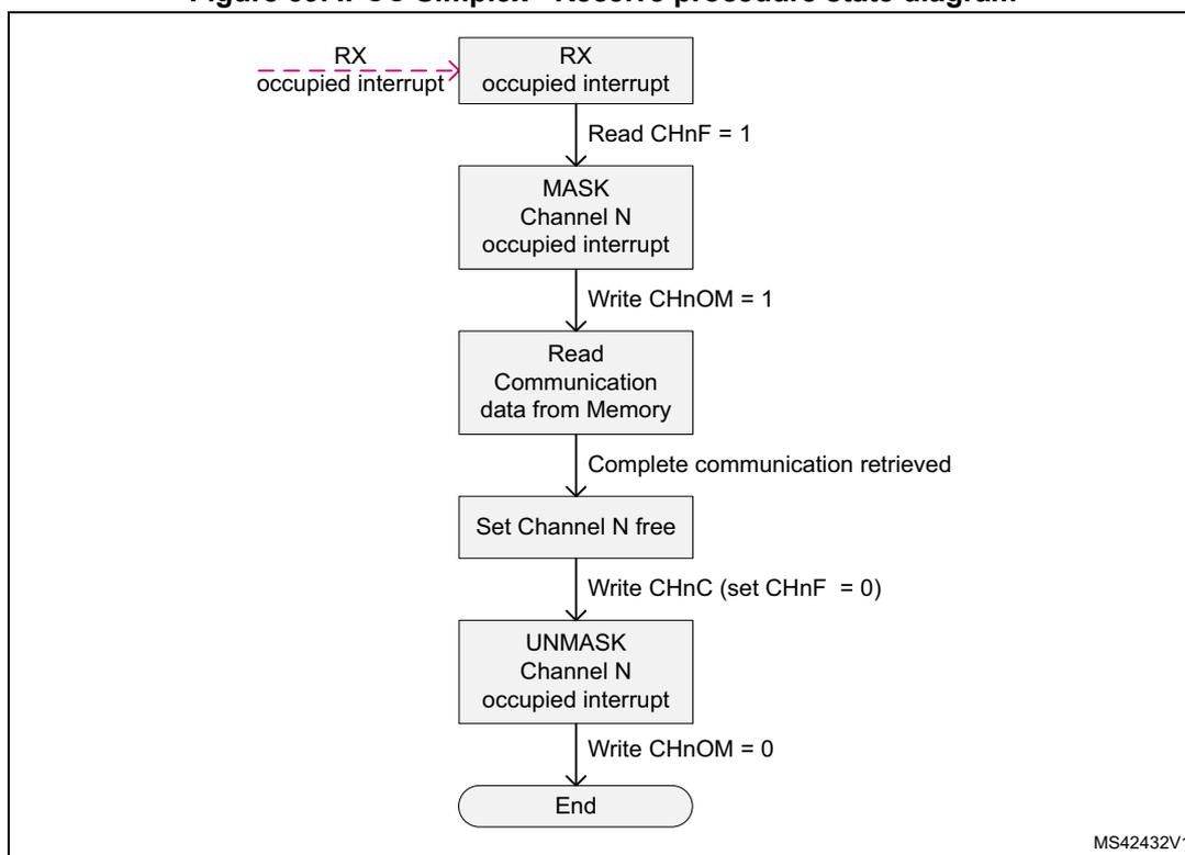
graph TD
    Start(( )) -.-> RX1[RX occupied interrupt]
    RX1 -- "Read CHnF = 1" --> MASK["MASK<br/>Channel N<br/>occupied interrupt"]
    MASK -- "Write CHnOM = 1" --> Read["Read<br/>Communication<br/>data from Memory"]
    Read -- "Complete communication retrieved" --> SetFree["Set Channel N free"]
    SetFree -- "Write CHnC (set CHnF = 0)" --> UNMASK["UNMASK<br/>Channel N<br/>occupied interrupt"]
    UNMASK -- "Write CHnOM = 0" --> End([End])
MS42432V1
To receive a communication, the channel occupied interrupt is unmasked ( \( CHnOM = 0 \) ):
- • On an RX occupied interrupt, the receiving processor checks which channel became occupied, masks the associated channel occupied interrupt ( \( CHnOM \) ) and reads the communication data from memory.
- • Once the complete communication data is retrieved, the channel status is cleared to free with \( CHnC \) . This gives memory access back to the sending processor and may generate the TX free interrupt.
- • Once the channel status is cleared, the channel occupied interrupt is unmasked ( \( CHnOM = 0 \) ).
9.3.3 IPCC Half-duplex channel mode
The Half-duplex channel mode is used when one processor sends a communication and the other processor sends a response to each communication (ping-pong).
In Half-duplex channel mode, a single dedicated memory location is assigned to communication data and response, and is used to transfer data in both directions. The sending processor channel status flag \( CHnF \) is assigned to the channel and used by both processors (see Table 68 ).
Once the processor A posts communication data into memory, it sets the processor A channel status flag \( CHnF \) to occupied with \( CHnS \) (giving memory access to processor B).
Once the processor B retrieves communication data from memory, it does not change the channel status flags. The memory access is kept by processor B for the response.
Once the processor B posts the response into memory, it clears the channel status flag \( CHnF \) to free with \( CHnC \) (giving memory access back to processor A).
Once the processor A retrieves the response from the memory, it does not change the channel status flags. The memory location access is kept by processor A for the next communication data.
Figure 40. IPCC Half-duplex channel mode transfer timing
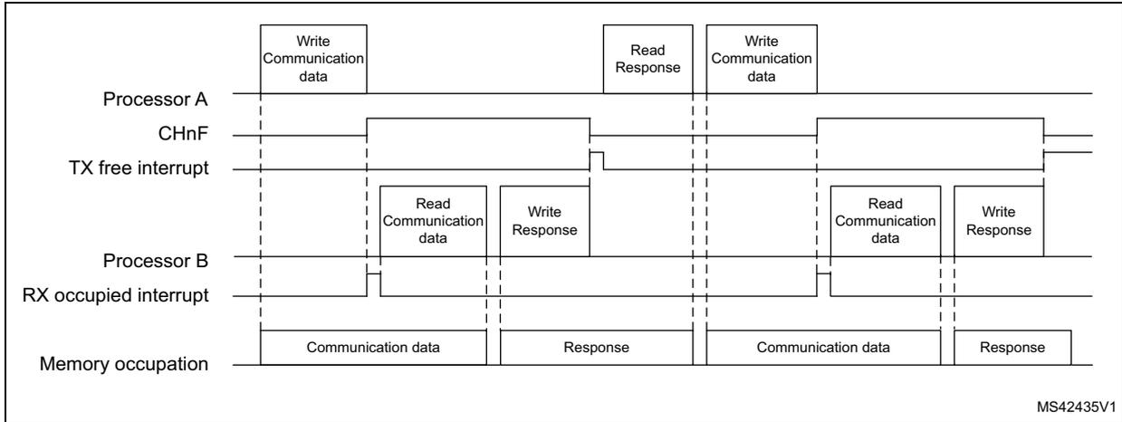
The diagram illustrates the timing for a half-duplex channel mode transfer. It shows the sequence of events for Processor A, Processor B, and Memory. Processor A writes communication data to memory, then later reads the response. Processor B reads the communication data and writes the response. The CHnF signal is shown as a pulse when the channel is free. The TX free interrupt is generated when the channel is free. The RX occupied interrupt is generated when the channel is occupied. The memory occupation shows the data and response being written and read.
MS42435V1
Figure 41. IPCC Half-duplex - Send procedure state diagram
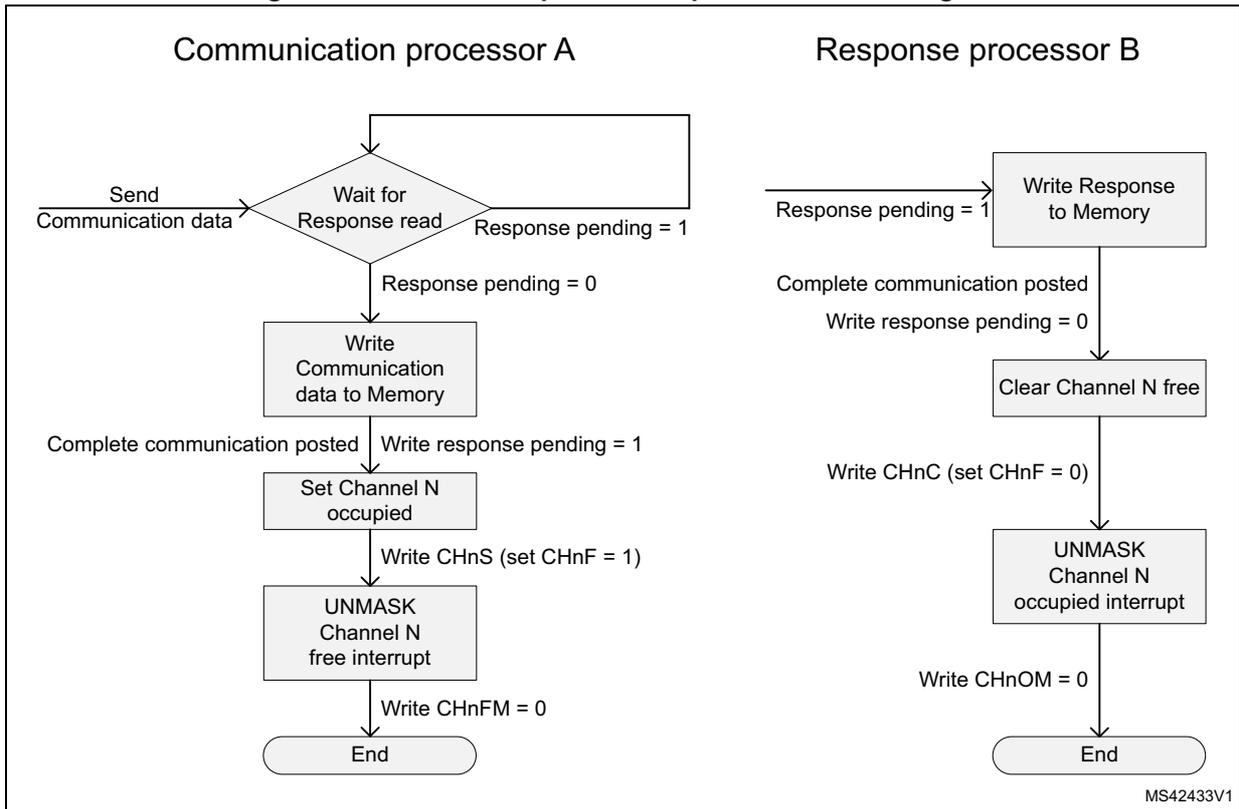
The diagram shows two state diagrams for the send procedure in half-duplex mode. The left diagram is for the Communication processor A, and the right diagram is for the Response processor B.
Communication processor A:
- Start: Send Communication data
- Decision: Wait for Response read
- If Response pending = 1, loop back to Wait for Response read.
- If Response pending = 0, proceed to Write Communication data to Memory.
- Action: Write Communication data to Memory
- Complete communication posted
- Write response pending = 1
- Action: Set Channel N occupied
- Action: Write CHnS (set CHnF = 1)
- Action: UNMASK Channel N free interrupt
- Action: Write CHnFM = 0
- End
Response processor B:
- Start: Response pending = 1
- Action: Write Response to Memory
- Complete communication posted
- Write response pending = 0
- Action: Clear Channel N free
- Action: Write CHnC (set CHnF = 0)
- Action: UNMASK Channel N occupied interrupt
- Action: Write CHnOM = 0
- End
MS42433V1
To send communication data:
- • The sending processor waits for its response pending software variable to get 0.
- – Once the response pending software variable is 0 the communication data is posted.
- • Once the complete communication data has been posted, the channel status flag CHnF is set to occupied with CHnS, and the response pending software variable is set to 1 (this gives memory access and generates the RX occupied interrupt to the receiving processor).
- • Once the channel status flag CHnF is set, the channel free interrupt is unmasked (CHnFM = 0).
To send a response:
- • The receiving processor waits for its response pending software variable to get 1.
- – Once the response pending software variable is 1, the response is posted.
- • Once the complete response is posted, the channel status flag CHnF is cleared to free with CHnC, and the response pending software variable is set to 0 (this gives memory access and generates the TX free interrupt to the sending processor).
- • Once the channel status flag CHnF is cleared, the channel occupied interrupt is unmasked (CHnOM = 0).
Figure 42. IPCC Half-duplex - Receive procedure state diagram
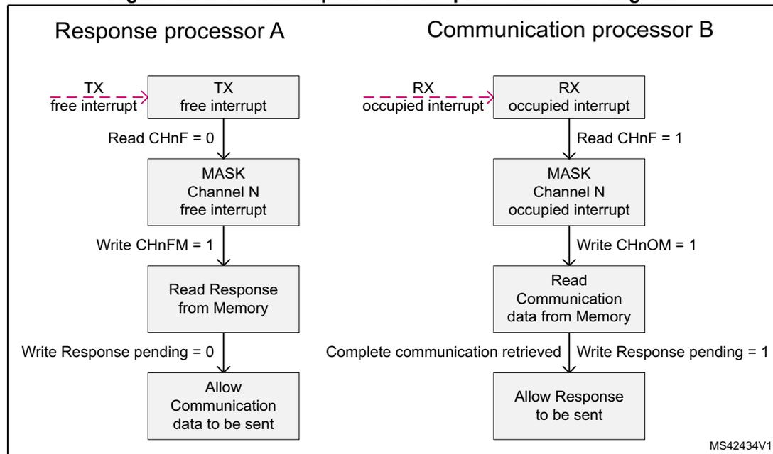
stateDiagram-v2
    state "Response processor A" as A
    state "Communication processor B" as B

    A: TX free interrupt --> A: TX free interrupt
    A: TX free interrupt --> A: Read CHnF = 0
    A: Read CHnF = 0 --> A: MASK Channel N free interrupt
    A: MASK Channel N free interrupt --> A: Write CHnFM = 1
    A: Write CHnFM = 1 --> A: Read Response from Memory
    A: Read Response from Memory --> A: Write Response pending = 0
    A: Write Response pending = 0 --> A: Allow Communication data to be sent

    B: RX occupied interrupt --> B: RX occupied interrupt
    B: RX occupied interrupt --> B: Read CHnF = 1
    B: Read CHnF = 1 --> B: MASK Channel N occupied interrupt
    B: MASK Channel N occupied interrupt --> B: Write CHnOM = 1
    B: Write CHnOM = 1 --> B: Read Communication data from Memory
    B: Read Communication data from Memory --> B: Complete communication retrieved
    B: Complete communication retrieved --> B: Write Response pending = 1
    B: Write Response pending = 1 --> B: Allow Response to be sent

    B: Complete communication retrieved --> A: Complete communication retrieved
To receive communication data the channel occupied interrupt is unmasked (CHnOM = 0):
- • On an RX occupied interrupt, the receiving processor checks which channel became occupied, masks the associated channel occupied interrupt (CHnOM) and reads the communication data from the memory.
- • Once the complete communication data is retrieved, the response pending software variable is set. The channel status is not changed, access to the memory is kept to post the subsequent response.
To receive the response the channel free interrupt is unmasked (CHnFM = 0):
- • On a TX free interrupt, the sending processor checks which channel became free, masks the associated channel free interrupt (CHnFM) and reads the response from the memory.
- • Once the complete response is retrieved, the response pending software variable is cleared. The channel status is not changed, access to the memory is kept to post the subsequent communication data.
9.3.4 IPCC interrupts
There are four interrupt lines :
- • two RX channel occupied interrupts, one for each processor:
- – Interrupt enable RXOIE per processor
- – Individual mask CHnOM per channel
- • two TX channel free interrupts, one for each processor
- – Interrupt enable TXFIE per processor
- – Individual mask CHnFM per channel
The RX occupied interrupt is used by the receiving processor and indicates when an unmasked channel status indicates occupied (CHnF = 1).
The TX free interrupt is used by the sending processor, and indicates when an unmasked channel status indicates free (CHnF = 0).
A secure channel only generates a secure interrupt, and only in the case when the channel is secure unmasked and global secure enabled.
A non-secure channel only generates a non-secure interrupt, and only in the case when the channel is non-secure unmasked and global non-secure enabled.
9.4 IPCC registers
The peripheral registers must be accessed by words (32-bit). Byte (8-bit) and half-word (16-bit) accesses are not permitted and do not generate a bus error.
9.4.1 IPCC processor 1 control register (IPCC_C1CR)
Address offset: 0x000
Reset value: 0x0000 0000
| 31 | 30 | 29 | 28 | 27 | 26 | 25 | 24 | 23 | 22 | 21 | 20 | 19 | 18 | 17 | 16 |
|---|---|---|---|---|---|---|---|---|---|---|---|---|---|---|---|
| Res. | Res. | Res. | Res. | Res. | Res. | Res. | Res. | Res. | Res. | Res. | Res. | Res. | Res. | Res. | TXFIE |
| rw | |||||||||||||||
| 15 | 14 | 13 | 12 | 11 | 10 | 9 | 8 | 7 | 6 | 5 | 4 | 3 | 2 | 1 | 0 |
| Res. | Res. | Res. | Res. | Res. | Res. | Res. | Res. | Res. | Res. | Res. | Res. | Res. | Res. | Res. | RXOIE |
| rw |
Bits 31:17 Reserved, must be kept at reset value.
Bit 16 TXFIE : Processor 1 transmit channel free interrupt enable
Associated with IPCC_C1TOC2SR.
1: Enable an unmasked processor 1 transmit channel free to generate a TX free interrupt.
0: Processor 1 TX free interrupt disabled
Bits 15:1 Reserved, must be kept at reset value.
Bit 0 RXOIE : Processor 1 receive channel occupied interrupt enable
Associated with IPCC_C2TOC1SR.
1: Enable an unmasked processor 1 receive channel occupied to generate an RX occupied interrupt.
0: Processor 1 RX occupied interrupt disabled
9.4.2 IPCC processor 1 mask register (IPCC_C1MR)
Address offset: 0x004
Reset value: 0xFFFF FFFF
| 31 | 30 | 29 | 28 | 27 | 26 | 25 | 24 | 23 | 22 | 21 | 20 | 19 | 18 | 17 | 16 |
|---|---|---|---|---|---|---|---|---|---|---|---|---|---|---|---|
| Res. | Res. | Res. | Res. | Res. | Res. | Res. | Res. | Res. | Res. | CH6 FM | CH5 FM | CH4 FM | CH3 FM | CH2 FM | CH1 FM |
| rw | rw | rw | rw | rw | rw | ||||||||||
| 15 | 14 | 13 | 12 | 11 | 10 | 9 | 8 | 7 | 6 | 5 | 4 | 3 | 2 | 1 | 0 |
| Res. | Res. | Res. | Res. | Res. | Res. | Res. | Res. | Res. | Res. | CH6 OM | CH5 OM | CH4 OM | CH3 OM | CH2 OM | CH1 OM |
| rw | rw | rw | rw | rw | rw |
Bits 31:22 Reserved, must be kept at reset value.
Bits 21:16 CHnFM : Processor 1 transmit channel n status set, (n = 6 to 1).
Associated with IPCC_C1TOC2SR.CHnF
1: Transmit channel n free interrupt masked.
0: Transmit channel n free interrupt not masked.
Bits 15:6 Reserved, must be kept at reset value.
Bits 5:0 CHnOM : Processor 1 receive channel n status clear (n = 6 to 1).
Associated with IPCC_C2TOC1SR.CHnF
1: Receive channel n occupied interrupt masked.
0: Receive channel n occupied interrupt not masked.
9.4.3 IPCC processor 1 status set clear register (IPCC_C1SCR)
Address offset: 0x008
Reset value: 0x0000 0000
Reading this register always returns 0x0000 0000.
| 31 | 30 | 29 | 28 | 27 | 26 | 25 | 24 | 23 | 22 | 21 | 20 | 19 | 18 | 17 | 16 |
|---|---|---|---|---|---|---|---|---|---|---|---|---|---|---|---|
| Res. | Res. | Res. | Res. | Res. | Res. | Res. | Res. | Res. | Res. | CH6S | CH5S | CH4S | CH3S | CH2S | CH1S |
| rw | rw | rw | rw | rw | rw | ||||||||||
| 15 | 14 | 13 | 12 | 11 | 10 | 9 | 8 | 7 | 6 | 5 | 4 | 3 | 2 | 1 | 0 |
| Res. | Res. | Res. | Res. | Res. | Res. | Res. | Res. | Res. | Res. | CH6C | CH5C | CH4C | CH3C | CH2C | CH1C |
| rw | rw | rw | rw | rw | rw |
Bits 31:22 Reserved, must be kept at reset value.
Bits 21:16 CHnS : Processor 1 transmit channel n status set (n = 6 to 1).
Associated with IPCC_C1TOC2SR.CHnF
1: Processor 1 transmit channel n status bit set.
0: No action.
Bits 15:6 Reserved, must be kept at reset value.
Bits 5:0 CHnC : Processor 1 receive channel n status clear (n = 6 to 1).
Associated with IPCC_C2TOC1SR.CHnF
1: Processor 1 receive channel n status bit clear.
0: No action.
9.4.4 IPCC processor 1 to processor 2 status register (IPCC_C1TOC2SR)
Address offset: 0x00C
Reset value: 0x0000 0000
| 31 | 30 | 29 | 28 | 27 | 26 | 25 | 24 | 23 | 22 | 21 | 20 | 19 | 18 | 17 | 16 |
|---|---|---|---|---|---|---|---|---|---|---|---|---|---|---|---|
| Res. | Res. | Res. | Res. | Res. | Res. | Res. | Res. | Res. | Res. | Res. | Res. | Res. | Res. | Res. | Res. |
| 15 | 14 | 13 | 12 | 11 | 10 | 9 | 8 | 7 | 6 | 5 | 4 | 3 | 2 | 1 | 0 |
| Res. | Res. | Res. | Res. | Res. | Res. | Res. | Res. | Res. | Res. | CH6F | CH5F | CH4F | CH3F | CH2F | CH1F |
| r | r | r | r | r | r |
Bits 31:6 Reserved, must be kept at reset value.
Bits 5:0 CHnF : Processor 1 transmit to processor 2 receive channel n status flag before masking (n = 6 to 1).
1: Channel occupied, data can be read by the receiving processor 2.
Generates a channel RX occupied interrupt to processor 2, when unmasked.
0: Channel free, data can be written by the sending processor 1.
Generates a channel TX free interrupt to processor 1, when unmasked.
9.4.5 IPCC processor 2 control register (IPCC_C2CR)
Address offset: 0x010
Reset value: 0x0000 0000
| 31 | 30 | 29 | 28 | 27 | 26 | 25 | 24 | 23 | 22 | 21 | 20 | 19 | 18 | 17 | 16 |
|---|---|---|---|---|---|---|---|---|---|---|---|---|---|---|---|
| Res. | Res. | Res. | Res. | Res. | Res. | Res. | Res. | Res. | Res. | Res. | Res. | Res. | Res. | Res. | TXFIE |
| nw | |||||||||||||||
| 15 | 14 | 13 | 12 | 11 | 10 | 9 | 8 | 7 | 6 | 5 | 4 | 3 | 2 | 1 | 0 |
| Res. | Res. | Res. | Res. | Res. | Res. | Res. | Res. | Res. | Res. | Res. | Res. | Res. | Res. | Res. | RXOIE |
| nw |
Bits 31:17 Reserved, must be kept at reset value.
Bit 16 TXFIE : Processor 2 transmit channel free interrupt enable
Associated with IPCC_C2TOC1SR.
1: Enable an unmasked processor 2 transmit channel free to generate a TX free interrupt.
0: Processor 2 TX free interrupt disabled
Bits 15:1 Reserved, must be kept at reset value.
Bit 0 RXOIE : Processor 2 receive channel occupied interrupt enable
Associated with IPCC_C1TOC2SR.
1: Enable an unmasked processor 2 receive channel occupied to generate an RX occupied interrupt.
0: Processor 2 RX occupied interrupt disabled
9.4.6 IPCC processor 2 mask register (IPCC_C2MR)
Address offset: 0x014
Reset value: 0xFFFF FFFF
| 31 | 30 | 29 | 28 | 27 | 26 | 25 | 24 | 23 | 22 | 21 | 20 | 19 | 18 | 17 | 16 |
|---|---|---|---|---|---|---|---|---|---|---|---|---|---|---|---|
| Res. | Res. | Res. | Res. | Res. | Res. | Res. | Res. | Res. | Res. | CH6 FM | CH5 FM | CH4 FM | CH3 FM | CH2 FM | CH1 FM |
| rw | rw | rw | rw | rw | rw |
| 15 | 14 | 13 | 12 | 11 | 10 | 9 | 8 | 7 | 6 | 5 | 4 | 3 | 2 | 1 | 0 |
|---|---|---|---|---|---|---|---|---|---|---|---|---|---|---|---|
| Res. | Res. | Res. | Res. | Res. | Res. | Res. | Res. | Res. | Res. | CH6 OM | CH5 OM | CH4 OM | CH3 OM | CH2 OM | CH1 OM |
| rw | rw | rw | rw | rw | rw |
Bits 31:22 Reserved, must be kept at reset value.
Bits 21:16 CHnFM : Processor 2 transmit channel n free interrupt mask (n = 6 to 1).
Associated with IPCC_C2TOC1SR.CHnF
1: Transmit channel n free interrupt masked.
0: Transmit channel n free interrupt not masked.
Bits 15:6 Reserved, must be kept at reset value.
Bits 5:0 CHnOM : Processor 2 receive channel n occupied interrupt mask (n = 6 to 1).
Associated with IPCC_C1TOC2SR.CHnF
1: Receive channel n occupied interrupt masked.
0: Receive channel n occupied interrupt not masked.
9.4.7 IPCC processor 2 status set clear register (IPCC_C2SCR)
Address offset: 0x018
Reset value: 0x0000 0000
Reading this register always returns 0x0000 0000.
| 31 | 30 | 29 | 28 | 27 | 26 | 25 | 24 | 23 | 22 | 21 | 20 | 19 | 18 | 17 | 16 |
|---|---|---|---|---|---|---|---|---|---|---|---|---|---|---|---|
| Res. | Res. | Res. | Res. | Res. | Res. | Res. | Res. | Res. | Res. | CH6S | CH5S | CH4S | CH3S | CH2S | CH1S |
| rw | rw | rw | rw | rw | rw |
| 15 | 14 | 13 | 12 | 11 | 10 | 9 | 8 | 7 | 6 | 5 | 4 | 3 | 2 | 1 | 0 |
|---|---|---|---|---|---|---|---|---|---|---|---|---|---|---|---|
| Res. | Res. | Res. | Res. | Res. | Res. | Res. | Res. | Res. | Res. | CH6C | CH5C | CH4C | CH3C | CH2C | CH1C |
| rw | rw | rw | rw | rw | rw |
Bits 31:22 Reserved, must be kept at reset value.
Bits 21:16 CHnS : Processor 2 transmit channel n status set (n = 6 to 1).
Associated with IPCC_C2TOC1SR.CHnF
1: Processor 2 transmit channel n status bit set.
0: No action.
Bits 15:6 Reserved, must be kept at reset value.
Bits 5:0 CHnC : Processor 2 receive channel n status clear (n = 6 to 1).
Associated with IPCC_C1TOC2SR.CHnF
1: Processor 2 receive channel n status bit clear.
0: No action.
9.4.8 IPCC processor 2 to processor 1 status register (IPCC_C2TOC1SR)
Address offset: 0x01C
Reset value: 0x0000 0000
| 31 | 30 | 29 | 28 | 27 | 26 | 25 | 24 | 23 | 22 | 21 | 20 | 19 | 18 | 17 | 16 |
|---|---|---|---|---|---|---|---|---|---|---|---|---|---|---|---|
| Res. | Res. | Res. | Res. | Res. | Res. | Res. | Res. | Res. | Res. | Res. | Res. | Res. | Res. | Res. | Res. |
| 15 | 14 | 13 | 12 | 11 | 10 | 9 | 8 | 7 | 6 | 5 | 4 | 3 | 2 | 1 | 0 |
| Res. | Res. | Res. | Res. | Res. | Res. | Res. | Res. | Res. | Res. | CH6F | CH5F | CH4F | CH3F | CH2F | CH1F |
| r | r | r | r | r | r |
Bits 31:6 Reserved, must be kept at reset value.
Bits 5:0 CHnF : Processor 2 transmit to processor 1 receive channel n status flag before masking (n = 6 to 1)
1: Channel occupied, data can be read by the receiving processor 1.
Generates a channel RX occupied interrupt to processor 1, when unmasked.
0: Channel free, data can be written by the sending processor 2.
Generates a channel TX free interrupt to processor 2, when unmasked.
9.4.9 IPCC register map
Table 69. IPCC register map and reset values
| Offset | Register name Reset value | 31 | 30 | 29 | 28 | 27 | 26 | 25 | 24 | 23 | 22 | 21 | 20 | 19 | 18 | 17 | 16 | 15 | 14 | 13 | 12 | 11 | 10 | 9 | 8 | 7 | 6 | 5 | 4 | 3 | 2 | 1 | 0 | |
|---|---|---|---|---|---|---|---|---|---|---|---|---|---|---|---|---|---|---|---|---|---|---|---|---|---|---|---|---|---|---|---|---|---|---|
| 0x0000 | IPCC_C1CR | Res. | Res. | Res. | Res. | Res. | Res. | Res. | Res. | Res. | Res. | Res. | Res. | Res. | Res. | Res. | TXFIE | Res. | Res. | Res. | Res. | Res. | Res. | Res. | Res. | Res. | Res. | Res. | Res. | Res. | Res. | Res. | Res. | RXOIE |
| Reset value | 0 | 0 | ||||||||||||||||||||||||||||||||
| 0x0004 | IPCC_C1MR | Res. | Res. | Res. | Res. | Res. | Res. | Res. | Res. | Res. | Res. | CH6FM | CH5FM | CH4FM | CH3FM | CH2FM | CH1FM | Res. | Res. | Res. | Res. | Res. | Res. | Res. | Res. | Res. | Res. | Res. | CH6OM | CH5OM | CH4OM | CH3OM | CH2OM | |
| Reset value | 1 | 1 | 1 | 1 | 1 | 1 | 1 | 1 | 1 | 1 | 1 | |||||||||||||||||||||||
| 0x0008 | IPCC_C1SCR | Res. | Res. | Res. | Res. | Res. | Res. | Res. | Res. | Res. | Res. | CH6S | CH5S | CH4S | CH3S | CH2S | CH1S | Res. | Res. | Res. | Res. | Res. | Res. | Res. | Res. | Res. | Res. | Res. | CH6C | CH5C | CH4C | CH3C | CH2C | |
| Reset value | 0 | 0 | 0 | 0 | 0 | 0 | 0 | 0 | 0 | 0 | 0 | |||||||||||||||||||||||
| 0x000C | IPCC_C1TOC2SR | Res. | Res. | Res. | Res. | Res. | Res. | Res. | Res. | Res. | Res. | Res. | Res. | Res. | Res. | Res. | Res. | Res. | Res. | Res. | Res. | Res. | Res. | Res. | Res. | Res. | Res. | CH6F | CH5F | CH4F | CH3F | CH2F | ||
| Reset value | 0 | 0 | 0 | 0 | 0 | |||||||||||||||||||||||||||||
| 0x0010 | IPCC_C2CR | Res. | Res. | Res. | Res. | Res. | Res. | Res. | Res. | Res. | Res. | Res. | Res. | Res. | Res. | Res. | TXFIE | Res. | Res. | Res. | Res. | Res. | Res. | Res. | Res. | Res. | Res. | Res. | Res. | Res. | Res. | Res. | RXOIE | |
| Reset value | 0 | 0 | ||||||||||||||||||||||||||||||||
| 0x0014 | IPCC_C2MR | Res. | Res. | Res. | Res. | Res. | Res. | Res. | Res. | Res. | Res. | CH6FM | CH5FM | CH4FM | CH3FM | CH2FM | CH1FM | Res. | Res. | Res. | Res. | Res. | Res. | Res. | Res. | Res. | Res. | Res. | CH6OM | CH5OM | CH4OM | CH3OM | CH2OM | |
| Reset value | 1 | 1 | 1 | 1 | 1 | 1 | 1 | 1 | 1 | 1 | 1 | |||||||||||||||||||||||
| 0x0018 | IPCC_C2SCR | Res. | Res. | Res. | Res. | Res. | Res. | Res. | Res. | Res. | Res. | CH6S | CH5S | CH4S | CH3S | CH2S | CH1S | Res. | Res. | Res. | Res. | Res. | Res. | Res. | Res. | Res. | Res. | Res. | CH6C | CH5C | CH4C | CH3C | CH2C | |
| Reset value | 0 | 0 | 0 | 0 | 0 | 0 | 0 | 0 | 0 | 0 | 0 | |||||||||||||||||||||||
| 0x001C | IPCC_C2TOC1SR | Res. | Res. | Res. | Res. | Res. | Res. | Res. | Res. | Res. | Res. | Res. | Res. | Res. | Res. | Res. | Res. | Res. | Res. | Res. | Res. | Res. | Res. | Res. | Res. | Res. | Res. | CH6F | CH5F | CH4F | CH3F | CH2F | ||
| Reset value | 0 | 0 | 0 | 0 | 0 |
Refer to Section 2.6 on page 72 for the register boundary addresses.