6. Power control (PWR)
6.1 Power supplies
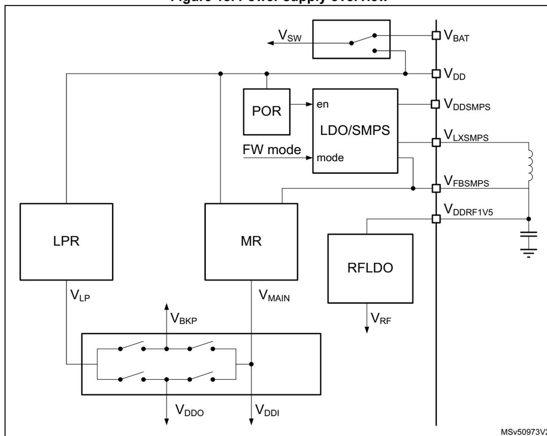
The STM32WL5x devices require a \( V_{DD} \) operating voltage supply between 1.71 V and 3.6 V. Several independent supplies ( \( V_{DDSMPS} \) , \( V_{FBSMPS} \) , \( V_{DDA} \) , \( V_{DDRF} \) ) can be provided for specific peripherals:
- • \( V_{DD} = 1.71 \text{ V} \) to \( 3.6 \text{ V} \)
\( V_{DD} \) is the external power supply for the I/Os, the system analog blocks such as reset, power management, internal clocks and low-power regulator. It is provided externally through VDD pins.
- • \( V_{DDSMPS} = 1.71 \text{ V} \) to \( 3.6 \text{ V} \)
\( V_{DDSMPS} \) is the external power supply for the SMPS step-down converter. It is provided externally through VDDSMPS supply pin and must be connected to the same supply as \( V_{DD} \) .
- • \( V_{FBSMPS} = 1.55 \text{ V} \)
\( V_{FBSMPS} \) is the external power supply for the main system regulator. It is provided externally through VFBSPS pin and is supplied through the SMPS step-down converter.
- • \( V_{DDA} = 0 \text{ V} \) to \( 3.6 \text{ V} \) (DAC/COMP minimum voltage is \( 1.62 \text{ V} \) , ADC minimum voltage is \( 1.8 \text{ V} \) and VREFBUF minimum voltage is \( 2.4 \text{ V} \) ).
\( V_{DDA} \) is the external analog power supply for A/D converters, D/A converters, voltage reference buffer, and comparators. The \( V_{DDA} \) voltage level is independent from the \( V_{DD} \) voltage (see power-up and power-down limitations below) and must preferably be connected to \( V_{DD} \) when these peripherals are not used.
- • \( V_{DDRF} = 1.71 \text{ V} \) to \( 3.6 \text{ V} \)
\( V_{DDRF} \) is the external power supply for the radio. It is provided externally through the VDDRF pin and must be connected to the same supply as \( V_{DD} \) .
- • \( V_{DDRF1V5} = 1.45 \text{ V} \) to \( 1.62 \text{ V} \)
\( V_{DDRF1V5} \) is the external power supply for the radio. It is provided externally through the VDDRF1V5 pin.
- • \( V_{BAT} = 1.55 \text{ V} \) to \( 3.6 \text{ V} \)
\( V_{BAT} \) is the power supply for RTC, TAMP, external clock 32 kHz oscillator and backup registers (through power switch) when \( V_{DD} \) is not present.
- • \( V_{REF-} \) , \( V_{REF+} \)
\( V_{REF+} \) is the input reference voltage for ADC. It is also the output of the internal voltage reference buffer when enabled.
- – When \( V_{DDA} < 2 \text{ V} \) , \( V_{REF+} \) must be equal to \( V_{DDA} \) .
- – When \( V_{DDA} \geq 2 \text{ V} \) , \( V_{REF+} \) must be between \( 2 \text{ V} \) and \( V_{DDA} \) .
\( V_{REF+} \) can be grounded when ADC is not active. The internal voltage reference buffer supports the following output voltages, configured with VRS bit in the VREFBUF_CSR register:
- – \( V_{REF+} \) around \( 2.048 \text{ V} \) : this requires \( V_{DDA} \geq 2.4 \text{ V} \) .
- – \( V_{REF+} \) around \( 2.5 \text{ V} \) : this requires \( V_{DDA} \geq 2.8 \text{ V} \) .
VREF+ pin is not available on all packages. When not available, this pin is internally bonded to VDDA. When VREF+ is double-bonded with VDDA in a package, the internal voltage reference buffer is not available and must be kept disabled (refer to the datasheet for pinout descriptions).
During power up and power down, the following power sequence is required:
- 1. When \( V_{DD} < 1 \) V other power supplies ( \( V_{DDA} \) ) must remain below \( V_{DD} + 300 \) mV.
During power down, \( V_{DD} \) can temporarily become lower than other supplies only if the energy provided to the device remains below 1 mJ. This allows external decoupling capacitors to be discharged with different time constants during this transient phase.
- 2. When \( V_{DD} > 1 \) V, all other power supplies ( \( V_{DDA} \) ) become independent.
An embedded linear voltage regulator is used to supply the internal digital power \( V_{CORE} \) . \( V_{CORE} \) is the power supply for digital peripherals, SRAM1 and SRAM2. The flash memory is supplied by \( V_{CORE} \) and \( V_{DD} \) . \( V_{CORE} \) is split in two parts: \( V_{DDO} \) part and an interruptible part \( V_{DDI} \) .
Figure 18. Power supply overview
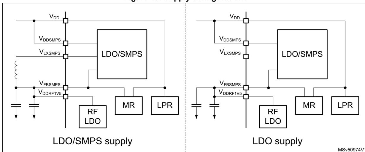
The different supply configurations are shown in the figure below.
Figure 19. Supply configurations
MSV50974V1
The LDO or SMPS step-down converter operating mode can be configured by one of the following:
- • by the MCU using the SMPSEN setting in PWR control register 5 (PWR_CR5) , that depends upon the MCU system operating mode (Run, Stop, Standby or Shutdown).
- • by the sub-GHz radio using Set_RegulatorMode() command and the sub-GHz radio operating mode (Sleep, Calibrate, Standby, Standby with HSE32 or Active).
After any POR and NRST reset, the LDO mode is selected. The SMPS selection has priority over LDO selection.
While the sub-GHz radio is in Standby with HSE32 or in Active mode, the supply mode is not altered until the sub-GHz radio enters Standby or Sleep mode. The sub-GHz radio activity may add a delay for entering the MCU software requested supply mode.
The LDO or SMPS supply mode can be checked with the SMPSRDY flag in Power status register 2 (PWR_SR2) .
Note: When the radio is active, the supply mode is not changed until after the radio activity is finished.
During Stop 1, Stop 2 and Standby modes, when the sub-GHz radio is not active, the LDO or SMPS step-down converter is switched off. When exiting low-power modes (except Shutdown), the SMPS step-down converter is set by hardware to the mode selected by the SMPSEN bit in PWR control register 5 (PWR_CR5) . SMPSEN is retained in Stop and Standby modes.
Independently from the MCU software selected supply operating mode, the sub-GHz radio allows the supply mode selection while the sub-GHz radio is active (thanks to the sub-GHz radio Set_RegulatorMode() command). For more details, see Relation between MCU and sub-GHz radio operating modes .
The maximum load current delivered by the SMPS can be selected by the sub-GHz radio SUBGHZ_SMPSC2R register. For more details see Section 5: Sub-GHz radio (SUBGHZ) .
The inrush current of the LDO and SMPS step-down converter can be controlled via the sub-GHz radio SUBGHZ_PCR register. This information is retained in all but the sub-GHz radio Deep-Sleep mode. For more details see Section 5: Sub-GHz radio (SUBGHZ) .
The SMPS needs a clock to be functional. If for any reason this clock stops, the device may be destroyed. It can be the case if the HSE is provided by an external clock source ( Figure 28: HSE32 clock sources ), with the risk that this clock disappears while the SMPS is enabled. To avoid this situation, a clock detection is used to, in case of a clock failure, switch off the SMPS and enable the LDO. The SMPS clock detection is enabled by the sub-GHz radio SUBGHZ_SMPS0R.CLKDE. By default, the SMPS clock detection is disabled and must be enabled before enabling the SMPS. For more details, see Section 5: Sub-GHz radio (SUBGHZ) .
6.1.1 Independent analog peripherals supply
To improve the ADC conversion accuracy and to extend the supply flexibility, the analog peripherals have an independent power supply that can be separately filtered and shielded from noise on the PCB.
The analog peripherals voltage supply input is available on a separate V DDA pin.
An isolated supply ground connection is provided on VSSA pin.
The V DDA supply voltage can be different from V DD . The presence of V DDA must be checked before enabling any of the analog peripherals supplied by V DDA (A/D converter, comparators, voltage reference buffer).
The V DDA supply can be monitored by the peripheral voltage monitoring, and compared with a threshold (1.65 V for PVM3). See Section 6.2.3: Peripheral voltage monitoring (PVM) for more details.
When a single supply is used, V DDA can be externally connected to V DD through the external filtering circuit in order to ensure a noise-free V DDA reference voltage.
ADC reference voltage
To ensure a better accuracy on low-voltage inputs and outputs, the user can connect a separate reference voltage lower than V DDA , to V REF+ . V REF+ is the highest voltage, represented by the full scale value, for an analog input (ADC) signal.
V REF+ can be provided either by an external reference or by an internal buffered voltage reference (VREFBUF).
The internal voltage reference is enabled by setting the ENVR bit in the VREFBUF control and status register (VREFBUF_CSR) . The voltage reference is set to 2.5 V when the VRS bit is set and to 2.048 V when the VRS bit is cleared. The internal voltage reference can also provide the voltage to external components through V REF+ pin. Refer to the device datasheet and to Voltage reference buffer (VREFBUF) for further information.
6.1.2 Battery backup domain
To retain the content of the backup registers and supply the RTC and TAMP functions when V DD is turned off, the VBAT pin can be connected to an optional backup voltage supplied by a battery or by another source.
The VBAT pin powers RTC, TAMP, the LSE oscillator and the PC13 to PC15 I/Os, allowing RTC and TAMP to operate even when the main power supply is turned off. The switch to the VBAT supply is controlled by the power-down reset embedded in the reset block.
Warning:
During
\(
t_{RSTTEMPO}
\)
(temporization at
\(
V_{DD}
\)
startup) or after a PDR is detected, the power switch between
\(
V_{BAT}
\)
and
\(
V_{DD}
\)
remains connected to
\(
V_{BAT}
\)
.
During the startup phase, if
\(
V_{DD}
\)
is established in less than
\(
t_{RSTTEMPO}
\)
(refer to the datasheet for the value of
\(
t_{RSTTEMPO}
\)
) and
\(
V_{DD} > V_{BAT} + 0.6
\)
V, a current can be injected into
\(
V_{BAT}
\)
through an internal diode connected between
\(
V_{DD}
\)
and the power switch (
\(
V_{BAT}
\)
).
If the power supply/battery connected to the VBAT pin cannot support this current injection, it is strongly recommended to connect an external low-drop diode between this power supply and the VBAT pin.
If no external battery is used in the application, it is recommended to connect VBAT externally to \( V_{DD} \) with a 100 nF external ceramic decoupling capacitor.
When the backup domain is supplied by \( V_{DD} \) (analog switch connected to \( V_{DD} \) ), the following pins are available:
- • PC13, PC14 and PC15, that can be used as GPIO pins
- • PC13, PC14 and PC15, that can be configured by RTC, TAMP or LSE (refer to Section 32: Real-time clock (RTC) and Section 33: Tamper and backup registers (TAMP) )
- • PA0/TAMP_IN2 and PB3/TAMP_IN3 when they are configured by the TAMP as tamper pins
Note: Due to the fact that the analog switch can transfer only a limited amount of current (3 mA), the use of GPIO PC13 to PC15 in output mode is restricted: the speed must be limited to 2 MHz with a maximum load of 30 pF and these I/Os must not be used as current source (e.g. to drive a LED).
When the backup domain is supplied by \( V_{BAT} \) (analog switch connected to \( V_{BAT} \) because \( V_{DD} \) is not present), the following functions are available:
- • PC13, PC14 and PC15 can be controlled only by RTC, TAMP or LSE (refer to Section 32: Real-time clock (RTC) and Section 33: Tamper and backup registers (TAMP) )
- • PA0/TAMP_IN2 and PB3/TAMP_IN3, when they are configured by the TAMP as tamper pins
Backup domain access
After a system reset, the backup domain (RTC and TAMP backup registers) is protected against possible unwanted write accesses. The DBP bit must be set in the PWR control register 1 (PWR_CR1) to enable access to the backup domain
VBAT battery charging
When \( V_{DD} \) is present, It is possible to charge the external battery on VBAT through an internal resistance.
The VBAT charging is done either through a 5 k \( \Omega \) resistor or through a 1.5 k \( \Omega \) resistor, depending on the VBRS bit value in the PWR control register 4 (PWR_CR4) .
The battery charging is enabled by setting VBE bit in the PWR control register 4 (PWR_CR4) , and automatically disabled in VBAT mode.
6.1.3 Voltage regulator
Two embedded linear voltage regulators supply all the digital circuitries, except for the Standby circuitry and the backup domain. The main regulator (MR) output voltage ( \( V_{CORE} \) ) can be programmed by software to two different power ranges (range 1 and range 2) to optimize the consumption depending on the system maximum operating frequency (refer to Section 7.2.9: Clock source frequency versus voltage scaling and to Section 4.3.4: Read access latency ).
The voltage regulators are always enabled after a reset. Depending on the application modes, the \( V_{CORE} \) supply is provided either by the main regulator or by the low-power regulator (LPR), as detailed below:
- • In Run, Sleep and Stop 0 modes, both regulators are enabled and the main regulator (MR) supplies full power to the \( V_{CORE} \) domain (core, memories and digital peripherals).
- • In LPRun and LPSleep modes, the main regulator (MR) is off and the low-power regulator (LPR) supplies reduced power to the \( V_{CORE} \) domain, preserving the contents of the registers and internal SRAM1 and SRAM2.
- • In Stop 1 and Stop 2 modes, the main regulator (MR) is off and the low-power regulator (LPR) supplies low power to the all or part of the \( V_{CORE} \) domain, preserving the contents of all or part of the registers and of internal SRAM1 and SRAM2.
- • In Standby modes with SRAM2 content preserved (RRS bit set in the PWR control register 3 (PWR_CR3) ), the main regulator (MR) is off and the low-power regulator (LPR) provides the supply to SRAM2 only. The core and digital peripherals (except Standby circuitry and backup domain), SRAM1 is powered off.
- • In Standby mode, both regulators (MR and LPR) are powered off. The contents of the registers and of SRAM1 and SRAM2 is lost except for the Standby circuitry and the backup domain.
- • In Shutdown mode, both regulators are powered off. When exiting from Shutdown mode, a power-on reset is generated. Consequently, the contents of the registers and of both SRAM1 and SRAM2 is lost, except for the backup domain.
6.1.4 Dynamic voltage scaling management
The dynamic voltage scaling is a power management technique that consists in increasing or decreasing the voltage used for the digital peripherals ( \( V_{CORE} \) ), according to the application performance and power consumption needs.
Dynamic voltage scaling to increase \( V_{CORE} \) is known as “overvolting”. It is used to improve the device performance.
Dynamic voltage scaling to decrease \( V_{CORE} \) is known as “undervolting”. It is used to save power, particularly in laptop and other mobile devices where the energy comes from a battery and is thus limited.
- • range 1: high-performance range
The main regulator provides a typical output voltage at 1.2 V. The system clock frequency can be up to 64 MHz. The flash memory access time for read access is minimum. Write and erase operations are possible.
- • range 2: low-power range
The main regulator provides a typical output voltage at 1.0 V. The system clock frequency can be up to 16 MHz. The flash memory access time for a read access is increased as compared to range 1. Write and erase operations are possible.
Voltage scaling is selected through the VOS bit in the PWR control register 1 (PWR_CR1) .
The sequence to go from range 1 to range 2 is the following:
- 1. Reduce the system frequency to a value lower or equal to 16 MHz.
- 2. Adjust number of wait states according to new frequency target in range 2 (LATENCY bits in the FLASH_ACR).
- 3. Select range 2 with the VOS bits in the PWR control register 1 (PWR_CR1) .
The sequence to go from range 2 to range 1 is detailed below:
- 1. Select range 1 in the VOS bits in the PWR control register 1 (PWR_CR1) .
- 2. Wait until the VOSF flag is cleared in the Power status register 2 (PWR_SR2) .
- 3. Adjust number of wait states according new frequency target in range 1 (LATENCY bits in the FLASH_ACR).
- 4. Increase the system frequency.
6.2 Power supply supervisor
6.2.1 Power-on reset (POR)/power-down reset (PDR)
/Brownout reset (BOR)
The device has an integrated power-on reset/power-down reset, coupled with a Brownout reset circuitry.
Five BOR thresholds can be selected through option bytes.
BOR0 level cannot be disabled. Other BOR levels can be enabled by user option. When enabled, BOR is active in all power modes except in Shutdown.
Reset mode
During power-on, BOR keeps the device under reset until the supply voltage \( V_{DD} \) reaches the specified \( V_{BORx} \) threshold. When \( V_{DD} \) drops below the selected threshold, a device reset is generated. When \( V_{DD} \) is above the \( V_{BORx} \) upper limit, the device reset is released and the system can start.
For more details on the Brownout reset thresholds, refer to the electrical characteristics section in the datasheet.
Figure 20. Brownout reset waveform
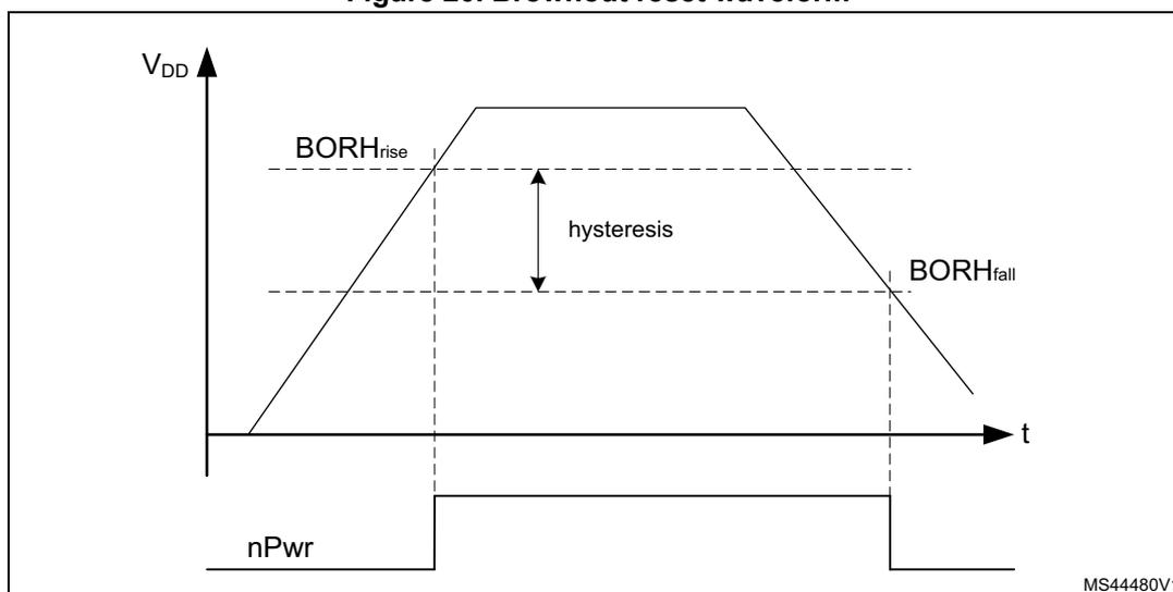
1. The reset temporization \( t_{RSTTEMPO} \) is present only for the BOR lowest threshold ( \( V_{BOR0} \) ).
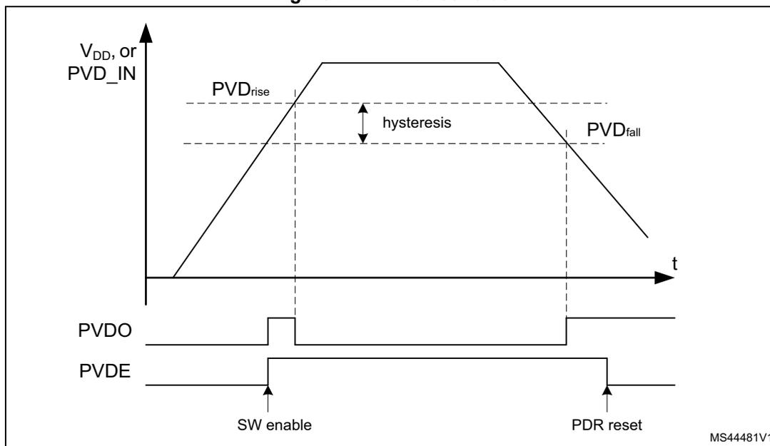
6.2.2 Programmable voltage detector (PVD)
The PVD can be used to monitor \( V_{DD} \) by comparing it to a threshold selected by the PLS[2:0] bits in the PWR control register 2 (PWR_CR2) .
PVD can also be used to monitor a voltage level on the PVD_IN pin. In this case the voltage level on PVD_IN is compared to the internal VREFINT level.
PVD is enabled by setting the PVDE bit.
A PVDO flag is available in the Power status register 2 (PWR_SR2) to indicate if \( V_{DD} \) or the voltage level on PVD_IN is higher or lower than the PVD threshold. This event is internally connected to the EXTI line 16 and can generate an interrupt if enabled through the EXTI registers.
The PVD output interrupt can be generated when \( V_{DD} \) or voltage level on PVD_IN drops below the PVD threshold and/or when \( V_{DD} \) or voltage level on PVD_IN rises above the PVD threshold depending on EXTI line 16 rising/falling edge configuration. As an example, the service routine can perform emergency shutdown tasks.
The PVD can be configured to monitor the \( V_{DD} \) supply level needed for the sub-GHz radio operation. For this, the PVD must select its lowest level and PVD and the wake-up must be enabled in EWPVD. Only a voltage drop below the PVD level generates a wake-up event.
BOR0 level cannot be disabled. The other BOR levels can be enabled by user option. When enabled, BOR is active in all power modes except in Shutdown.
Figure 21. PVD thresholds
6.2.3 Peripheral voltage monitoring (PVM)
Only \( V_{DD} \) is monitored by default as it is the only supply required for all system-related functions. The other supplies (such as \( V_{DDA} \) ) can be independent from \( V_{DD} \) and can be monitored by the peripheral voltage monitoring (PVM).
Each PVMx is a comparator between a fixed threshold \( V_{PVMx} \) and the selected power supply. PVMOx flags indicate if the independent power supply is higher or lower than the PVMx threshold. The PVMOx flag is cleared when the supply voltage is above the PVMx threshold and is set when the supply voltage is below the PVMx threshold.
Each PVM output is connected to an EXTI line and can generate an interrupt if enabled through the EXTI registers. The PVMx output interrupt is generated when the independent power supply drops below the PVMx threshold and/or when it rises above the PVMx threshold, depending on EXTI line rising/falling edge configuration.
Each PVM can remain active in Stop 0, Stop 1 and Stop 2 modes, and the PVM interrupt can wake up from the Stop modes.
Table 43. PVM features
| PVM | Power supply | PVM threshold | EXTI line |
|---|---|---|---|
| PVM1 | Not used | - | - |
| PVM2 | Not used | - | - |
| PVM3 | \( V_{DDA} \) | \( V_{PVM3} \) (around 1.65 V) | 34 |
| PVM4 | Not used | - | - |
The independent supply \( V_{DDA} \) is not considered as present by default and a logical and electrical isolation is applied to ignore any information coming from the peripherals supplied by these dedicated supplies:
- • If \( V_{DDA} \) is shorted externally to \( V_{DD} \) , the application must assume that \( V_{DDA} \) is available without enabling any peripheral voltage monitoring.
- • If \( V_{DDA} \) is independent from \( V_{DD} \) , the peripheral voltage monitoring (PVM) can be enabled to confirm whether the \( V_{DDA} \) supply is present or not.
The following sequence must be applied before using any of these analog peripherals: ADC, DAC, comparators or voltage reference buffer:
- 1. If
\(
V_{DDA}
\)
is independent from
\(
V_{DD}
\)
:
- a) Enable PVM3 by setting PVME3 bit in the PWR control register 2 (PWR_CR2) .
- b) Wait for the PVM3 wake-up time.
- c) Wait until PVMO3 is cleared in the Power status register 2 (PWR_SR2) .
- d) Disable the PVM3 for consumption saving (optional).
- 2. Enable the analog peripheral. This automatically removes the \( V_{DDA} \) isolation.
6.2.4 Radio end of life (EOL)
The radio end-of-life monitor provides information on the \( V_{DD} \) supply when it is too low to operate the sub-GHz radio. When reaching the EOL level, the software must stop all radio activities in a safe way.
The EOL is enabled by setting the RFEOLEN bit.
The RFEOLF flag is available in Power status register 2 (PWR_SR2) to indicate if \( V_{DD} \) voltage level is below the EOL threshold.
The EOL is only generated when the sub-GHz radio is in Calibrate, Standby or Active mode.
Figure 22. EOL thresholds
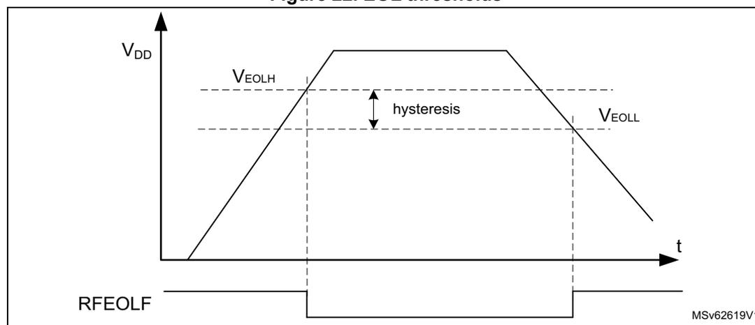
The figure is a graph showing the relationship between the \( V_{DD} \) supply voltage and the RFEOLF flag status over time ( \( t \) ). The vertical axis represents \( V_{DD} \) and the horizontal axis represents time ( \( t \) ). The voltage curve shows a rise to a peak followed by a fall. Two horizontal dashed lines represent the EOL thresholds: \( V_{EOLH} \) (higher threshold) and \( V_{EOLL} \) (lower threshold). The RFEOLF flag is shown as a digital signal that goes low when the voltage drops below \( V_{EOLL} \) and returns high when it rises above \( V_{EOLH} \) . The hysteresis between \( V_{EOLH} \) and \( V_{EOLL} \) is indicated by a double-headed arrow. The figure is labeled MSV62619V1.
6.3 Radio busy management
For correct software handling of the radio busy signal RFBUSY, additional busy control are included in the PWR controller. This generates a busy mask RFBUSYMS status based on
the SUBGHZSPI_NSS activity, and masks the RFBUSYS status low time (not busy) after an SPI command transfer (see the figure below).
Figure 23. Radio busy management
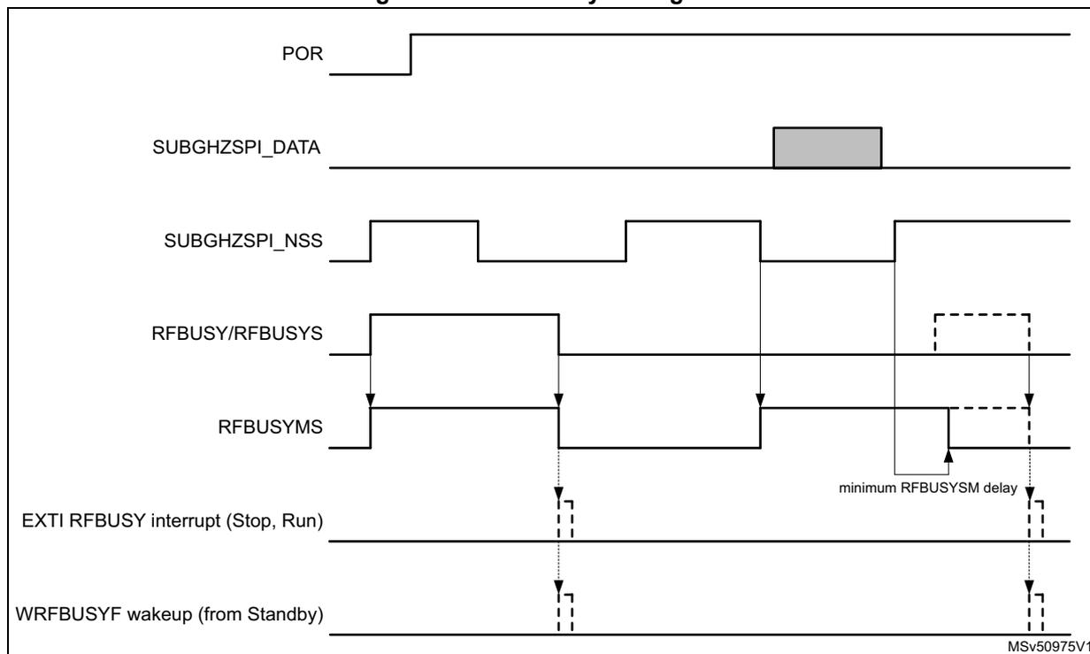
At reset, the radio is busy (as signaled by the RFBUSY signal). At this time, the RFBUSYMS signal provides the same information. Subsequently the radio is woken up by a falling edge on SUBGHZSPI_NSS. Once the radio is ready to receive a command, RFBUSYS and RFBUSYMS go low. After reset, the RFBUSYS or RFBUSYMS status can be used to check that the radio is ready.
For any subsequent command, as soon as the SUBGHZSPI_NSS goes low, the RFBUSYMS status is set to signal busy radio. RFBUSYMS remains high for at least the minimum RFBUSYMS delay after the SUBGHZSPI_NSS is set high, or as long as the RFBUSY signal remains high:
- • When transferring a command with an expected radio busy indication the RFBUSYMS status must be used to detect the radio busy state.
- • When transferring a command without any expected radio busy indication, there is no need for checking any busy status. A new command can be sent even when RFBUSYMS status indicates busy radio.
When the SUBGHZSPI_NSS is selected to be driven by the LPTIM3_OUT in PWR_CR1.SUBGHZPINSSSEL, the RFBUSYMS status is disabled and must not be used by software.
When in Standby mode, the CPUs can be woken up through a WRFBUSYF wake-up flag when enabled by EWRFBUSY in Section 6.6.3: PWR control register 3 (PWR_CR3) or Section 6.6.18: PWR CPU2 control register 3 (PWR_C2CR3) .
When in Stop or Run mode, a CPU can be woken up and interrupted by the EXTI configurable event on the RFBUSY signal, see Section 16.3.1: EXTI wake-up interrupt list .
6.4 CPU2 boot
The CPU2 boot is controlled by the following sources:
- • from C2BOOT bit in PWR control register 4 (PWR_CR4)
This allows the CPU1 to initialize the system after a reset or wake-up from system Low-power mode, before booting the CPU2.
- • when the system is secure (ESE = 1), from any illegal access wake-up event before C2BOOT is set to 1 by the CPU1
This guarantees that the secure CPU2 is informed of any illegal access before it is booted by C2BOOT.
Following reset, CPU2 is prevented from booting by the C2BOOT bit (except when booting the device in RSS/SFI mode). Only once the CPU1 set the C2BOOT bit or if an illegal access event is detected, CPU2 boots.
When exiting system low-power modes (Stop 0, 1, 2 or Standby), the CPU2 boot can be controlled by the C2BOOT bit as follows:
- • C2BOOT = 1: When exiting a system low-power mode, CPU2 boots when it is woken up via a wake-up source.
- • C2BOOT = 0: When exiting a system low-power mode, CPU2 is prevented from booting, except when the system is secure and an illegal access wake-up event is detected. On any CPU2 wake-up source other than an illegal access wake-up event, CPU1 is woken up via a C2HF. It is then up to CPU1 to boot CPU2 by setting the C2BOOT bit.
In a secure system, when booting the CPU2 due to an illegal access, the C2BOOTS flag indicates so and the illegal access source is set in the ILAC status register. CPU2 keeps booting due to an illegal access even after a system reset. However, in this case, the illegal access source in the ILAC status register is cleared. The system stops booting the CPU2 due to an illegal access, only when the CPU2 enters CStop mode or after a POR reset.
When C2BOOT is set while the CPU2 has been boot due to an illegal access (C2BOOTS), this illegal access boot must first be completed by having the CPU2 entering CStop mode. This clears the illegal access boot mode and causes the CPU2 to restart in normal boot mode.
Figure 24. CPU2 boot options
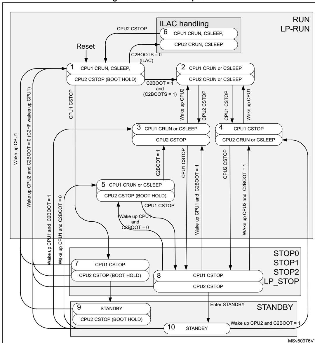
The diagram illustrates the boot options for CPU2 based on the state of CPU1 and the configuration bits C2BOOT and C2BOOTS. It is organized into three main power modes: RUN/LP-RUN, STOP0/STOP1/STOP2/LP_STOP, and STANDBY.
- RUN/LP-RUN Mode:
- State 1: CPU1 CRUN, CSLEEP; CPU2 CSTOP (BOOT HOLD). Entered via Reset or CPU2 CSTOP. Transitions to State 2 if C2BOOT = 1 and (C2BOOTS = 1). Transitions to State 3 if CPU1 CSTOP. Transitions to State 5 if CPU1 CSTOP. Transitions to State 7 if CPU1 CSTOP. Transitions to State 9 if CPU1 CSTOP. Transitions to State 10 if CPU1 CSTOP.
- State 2: CPU1 CRUN or CSLEEP; CPU2 CRUN or CSLEEP. Entered from State 1. Transitions to State 3 if CPU2 CSTOP. Transitions to State 4 if CPU2 CSTOP. Transitions to State 8 if CPU2 CSTOP.
- State 3: CPU1 CRUN or CSLEEP; CPU2 CSTOP. Entered from State 1 or State 2. Transitions to State 2 if C2BOOT = 1 and (C2BOOTS = 1). Transitions to State 5 if C2BOOT = 1. Transitions to State 8 if CPU1 CSTOP.
- State 4: CPU1 CSTOP; CPU2 CRUN or CSLEEP. Entered from State 2. Transitions to State 3 if CPU1 CSTOP. Transitions to State 5 if CPU1 CSTOP. Transitions to State 8 if CPU1 CSTOP.
- State 5: CPU1 CRUN or CSLEEP; CPU2 CSTOP (BOOT HOLD). Entered from State 1 or State 3. Transitions to State 2 if CPU1 CSTOP. Transitions to State 8 if CPU1 CSTOP.
- State 7: CPU1 CSTOP; CPU2 CSTOP (BOOT HOLD). Entered from State 1. Transitions to State 8 if CPU1 CSTOP.
- State 8: CPU1 CSTOP; CPU2 CSTOP. Entered from State 2, 3, 4, 5, or 7. Transitions to State 9 if CPU1 CSTOP.
- State 9: STANDBY; CPU2 CSTOP (BOOT HOLD). Entered from State 1 or State 8. Transitions to State 10 if CPU1 CSTOP.
- State 10: STANDBY. Entered from State 1, 9, or 10. Transitions to State 1 if Wake up CPU2 and C2BOOT = 0 (C2HF wakes up CPU1). Transitions to State 2 if Wake up CPU1 and C2BOOT = 1. Transitions to State 3 if Wake up CPU1 and C2BOOT = 0. Transitions to State 4 if Wake up CPU2 and C2BOOT = 1.
- STOP0/STOP1/STOP2/LP_STOP Mode:
- State 7: CPU1 CSTOP; CPU2 CSTOP (BOOT HOLD). Entered from State 1. Transitions to State 8 if CPU1 CSTOP.
- State 8: CPU1 CSTOP; CPU2 CSTOP. Entered from State 2, 3, 4, 5, 7, or 9. Transitions to State 9 if CPU1 CSTOP.
- STANDBY Mode:
- State 9: STANDBY; CPU2 CSTOP (BOOT HOLD). Entered from State 1 or State 8. Transitions to State 10 if CPU1 CSTOP.
- State 10: STANDBY. Entered from State 1, 9, or 10. Transitions to State 1 if Wake up CPU2 and C2BOOT = 0 (C2HF wakes up CPU1). Transitions to State 2 if Wake up CPU1 and C2BOOT = 1. Transitions to State 3 if Wake up CPU1 and C2BOOT = 0. Transitions to State 4 if Wake up CPU2 and C2BOOT = 1.
ILAC handling: CPU2 CSTOP leads to ILAC handling (6). CPU1 CRUN, CSLEEP; CPU2 CRUN, CSLEEP. C2BOOTS = 0 (ILAC).
MSv50976V1
When CPU1 is used to initialize the system before CPU2 is booted, the procedure is the following:
- • Before CPU1 enters CStop mode, it clears the C2BOOT bit.
- • When CPU1 exits CStop:
- – The system remains in Run mode and sets the C2BOOT bit, subsequently processing the wake-up event.
- – The system exits a low-power mode from a CPU1 wake-up source. This initializes the system and sets the C2BOOT bit, subsequently processing the wake-up event.
- – The system exits a low-power mode from a CPU2 wake-up source. The C2HF wake-up source wakes up CPU1, that initializes the system and sets the C2BOOT bit. CPU1 subsequently goes back to CStop. After C2BOOT is set, CPU2 is woken up by its wake-up source.
When CPU2 is prevented from booting (C2BOOT = 0, boot hold), the wake-up from low-power mode boot procedure is the following:
- • When the system is secure (ESE = 1) and the secure CPU2 boots after reset (POR/NRST or wake-up from Standby), CPU2 checks the reset source (C2BOOT or illegal access) in the C2BOOTS bit, as follows:
- – C2BOOTS = 1: The secure CPU2 boots from C2BOOT and the normal application is started.
- – C2BOOTS = 0: The secure CPU2 boots due to an illegal access. In this case CPU2 processes the illegal access and reenters CStop mode. This sets CPU2 back in reset and clears the C2BOOTS flag.
- • When waking up from CStop mode, CPU2 checks the wake-up source (C2BOOT or illegal access) as follows:
- – C2BOOTS = 1: The secure CPU2 is re-started by C2BOOT and the normal application is started. The system is initialized by CPU1. So CPU2 can directly process the wake-up event
- – C2BOOTS = 0: The secure CPU2 restarts due to an illegal access. In this case, CPU2 processes the illegal access and reenters CStop mode. This sets CPU2 back in CStop mode.
When the system remains in Run mode (due to one CPU), the other CPU wakes up from CStop mode without the system having gone to a low-power mode.
6.5 Low-power modes
By default, the microcontroller is in Run mode after a system or a power reset and at least one of the CPUs is in CRun mode executing code. Low-power modes are available to save power when the CPU does not need to be kept running, for example when it is waiting for an external event. The user must select the mode giving the best compromise between consumption, startup time and available wake-up sources.
Each CPU features the following low-power modes, that are entered by the CPU when executing WFI, WFE or on return from an exception handler when SLEEPONEXIT in the CPU is enabled:
- • CSleep mode: when CPU enters low-power mode and the CPU SLEEPDEEP is disabled
- • CStop mode: when CPU enters low-power mode and the CPU SLEEPDEEP is enabled
These low-power modes are detailed below:
- • Sleep mode : CPU clock off, all peripherals including CPU core peripherals (among them NVIC, SysTick) can run and wake up the CPU when an interrupt or an event occurs.
- • Low-power run mode (LPRun) : when the system clock frequency is reduced below 2 MHz. The code is executed from the SRAM or from the flash memory. The regulator is in low-power mode to minimize the operating current.
- • Low-power sleep mode (LPSleep) : entered from the LPRun mode.
- • Stop 0 mode , and Stop 1 mode : the content of SRAM1, SRAM2 and of all registers is retained. All clocks in the V CORE domain are stopped. PLL, MSI, HSI16 and HSE32 are disabled. LSI and LSE can be kept running.
RTC can remain active (Stop mode with RTC, Stop mode without RTC). The sub-GHz
radio may remain active independently from the CPUs.
Some peripherals with the wake-up capability can enable HSI16 RC during the Stop mode to detect their wake-up condition.
Stop 1 offers the largest number of active peripherals and wake-up sources, a smaller wake-up time but a higher consumption compared with Stop 2.
In Stop 0 mode, the main regulator remains on, resulting in the fastest wake-up time but with much higher consumption. The active peripherals and wake-up sources are the same as in Stop 1 mode that uses the low-power regulator.
The system clock, when exiting Stop 0 or Stop 1 mode, can be either MSI up to 48 MHz or HSI16, depending on the software configuration.
- • Stop 2 mode: part of the \( V_{\text{CORE}} \) domain is powered off. Only SRAM1, SRAM2, CPUs and some peripherals preserve their contents (see Table 45: Functionalities depending on system operating mode ).
All clocks in the \( V_{\text{CORE}} \) domain are stopped. PLL, MSI, HSI16 and HSE32 are disabled. LSI and LSE can be kept running.
RTC can remain active (Stop 2 mode with RTC, Stop 2 mode without RTC). The sub-GHz radio may also remain active independent from the CPUs.
Some peripherals with the wake-up capability can enable HSI16 RC during the Stop 2 mode to detect their wake-up condition (see Table 45: Functionalities depending on system operating mode ).
The system clock when exiting from Stop 2 mode, can be either MSI up to 48 MHz or HSI16, depending on the software configuration.
- •
Standby mode:
\(
V_{\text{CORE}}
\)
domain is powered off. However, it is possible to preserve the SRAM2 content as detailed below:
- – Standby mode with SRAM2 retention when the RRS bit is set in the PWR control register 3 (PWR_CR3) . In this case, SRAM2 is supplied by the low-power regulator.
- – Standby mode when the RRS bit is cleared in the PWR control register 3 (PWR_CR3) . In this case the main regulator and the low-power regulator are powered off.
All clocks in the \( V_{\text{CORE}} \) domain are stopped. PLL, MSI, HSI16 and HSE32 are disabled. LSI and LSE can be kept running.
The RTC can remain active (Standby mode with RTC, Standby mode without RTC). The sub-GHz radio and the PVD may also remain active when enabled independent from the CPUs. In Standby mode, the PVD selects its lowest level.
The system clock, when exiting Standby modes, is MSI at 4 MHz.
- • Shutdown mode: \( V_{\text{CORE}} \) domain is powered off. All clocks in the \( V_{\text{CORE}} \) domain are stopped. PLL, MSI, HSI16, LSI and HSE32 are disabled. LSE can be kept running. The system clock when exiting the Shutdown mode, is MSI at 4 MHz. In this mode, the supply voltage monitoring is disabled and the product behavior is not guaranteed in case of a power voltage drop.
Note: Stop, Standby and Shutdown modes are only entered when both CPUs are in CStop mode. When the device boot in RSS/SFI mode, the low-power modes Stop, Standby and Shutdown, cannot be entered.
In addition, the power consumption in Run mode can be reduced by slowing down the system clocks, and/or by gating the clocks to the APB and AHB peripherals when they are unused.
The system operation mode depends on the CPU1 and the CPU2 sub-system operating mode. The system only enters a low-power mode when both sub-systems allow it to do so.
After a system reset, CPU1 is in CRUN mode. CPU2 only boots if enabled by CPU1 via the C2BOOT bit, or when the system is secure on an illegal access detection. As long as CPU1 does not boot CPU2, the device operates as a single CPU system. CPU1 can enter and wake up from system low-power modes on its own.
When CPU2 has boot, CPU1, CPU2 and radio sub-systems can enter and wake up from system low-power modes on their own.
The system low-power mode to enter depends on the allowed mode selected by the CPUs in LPMS[2:0] bits in PWR control register 1 (PWR_CR1) and PWR CPU2 control register 1 (PWR_C2CR1) .
Figure 25 shows the operating modes state diagram. CPU1 and CPU2 sub-systems operate interdependently according to their own sub-system states. Each sub-system has its own wake-up sources, that allow it to wake up from Stop and Standby modes. For the device to be in Stop, Standby or Shutdown mode, both sub-systems must be in CStop. When one sub-system enters CRun mode, the device enters Run mode.
Figure 25. CPUs low-power modes possible transitions
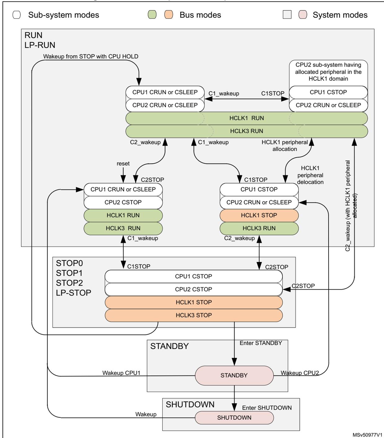
Legend:
- □ Sub-system modes
- ● Bus modes
- □ System modes
States:
- RUN / LP-RUN (Sub-system modes):
- Left state: CPU1 CRUN or CSLEEP, CPU2 CRUN or CSLEEP, HCLK1 RUN, HCLK3 RUN.
- Right state: CPU1 CSTOP, CPU2 CRUN or CSLEEP, HCLK1 RUN, HCLK3 RUN. (Note: CPU2 sub-system having allocated peripheral in the HCLK1 domain)
- STOP0 / STOP1 / STOP2 / LP-STOP (Sub-system modes):
- Left state: CPU1 CRUN or CSLEEP, CPU2 CSTOP, HCLK1 RUN, HCLK3 RUN.
- Right state: CPU1 CSTOP, CPU2 CRUN or CSLEEP, HCLK1 STOP, HCLK3 RUN.
- STANDBY (System modes):
- Single state: STANDBY.
- SHUTDOWN (System modes):
- Single state: SHUTDOWN.
Transitions:
- From RUN/LP-RUN to STOP0/STOP1/STOP2/LP-STOP:
- From left to right: C2STOP, reset.
- From right to left: C1STOP.
- From STOP0/STOP1/STOP2/LP-STOP to RUN/LP-RUN:
- From left to right: C1_wakeup.
- From right to left: C2_wakeup, C1_wakeup.
- From RUN/LP-RUN to STANDBY:
- From right state: Enter STANDBY.
- From STANDBY to RUN/LP-RUN:
- Wakeup CPU1 to left state.
- Wakeup CPU2 to right state.
- From RUN/LP-RUN to SHUTDOWN:
- Wakeup from STOP with CPU HOLD to left state.
- From SHUTDOWN to RUN/LP-RUN:
- Wakeup to left state.
- Internal Transitions in RUN/LP-RUN:
- Left to right: C1_wakeup, C1STOP.
- Right to left: C2_wakeup, C1_wakeup, HCLK1 peripheral allocation, HCLK1 peripheral deallocation, C2STOP.
MSv50977V1
Table 44. Low-power mode summary
| Mode name | Entry | Wake-up source (1) | Wake-up system clock | Effect on clocks | Voltage regulators | |
|---|---|---|---|---|---|---|
| MR | LPR | |||||
| Sleep (Sleep-now or Sleep-on-exit) | WFI or return from ISR | Any interrupt | Same as before entering Sleep mode | CPU clock OFF No effect on other clocks or analog clock sources | ON | ON |
| WFE | Wake-up event | |||||
| LPRun | Set LPR bit | Clear LPR bit | Same as LPRun clock | None | OFF | ON |
| LPSleep | Set LPR bit + WFI or return from ISR | Any interrupt | Same as before entering LPSleep mode | CPU clock OFF No effect on other clocks or analog clock sources | OFF | ON |
| Set LPR bit + WFE | Wake-up event | OFF | ON | |||
| Stop 0 | LPMS = 0b000 + SLEEPDEEP bit + WFI or return from ISR or WFE | Any EXTI line (configured in the EXTI registers). Specific peripherals events | HSI16 when STOPWUCK = 1 in RCC_CFGR. MSI with the frequency before entering the Stop mode when STOPWUCK = 0. | All clocks OFF except HSI16, LSI and LSE | ON | ON |
| Stop 1 | LPMS = 0b001 + SLEEPDEEP bit + WFI or return from ISR or WFE | OFF | ||||
| Stop 2 (with I2C3, LPUART1, LPTIM1, SRAM1, SRAM2) | LPMS = 0b010+ SLEEPDEEP bit + WFI or return from ISR or WFE | |||||
| Standby (with SRAM2) | LPMS = 0b011+ Set RRS bit + SLEEPDEEP bit + WFI or return from ISR or WFE | Wake-up PVD, RFIRQ, wake-up RFBUSY, WKUP pin edge, RTC and TAMP event, LSECSS, external reset in NRST pin, IWDG reset | MSI 4 MHz | All clocks OFF except LSI and LSE | OFF | OFF |
| Standby | LPMS = 0b011 + Clear RRS bit + SLEEPDEEP bit + WFI or return from ISR or WFE | |||||
| Shutdown | LPMS = 0b1xx + SLEEPDEEP bit + WFI or return from ISR or WFE | WKUP pin edge, RTC and TAMP event, external reset in NRST pin | MSI 4 MHz | All clocks OFF except LSE | OFF | OFF |
1. Refer to Table 45: Functionalities depending on system operating mode .
Table 45. Functionalities depending on system operating mode (1)| Peripheral | Run | Sleep | LPRun | LPSleep | Stop 0 | Stop 1 | Stop 2 | Standby | Shutdo | VBAT | |||||
|---|---|---|---|---|---|---|---|---|---|---|---|---|---|---|---|
| - | Wake-up capability | - | Wake-up capability | - | Wake-up capability | - | Wake-up capability | - | Wake-up capability | ||||||
| CPU1 | Y | - | Y | - | R | - | R | - | R | - | - | - | - | - | - |
| CPU2 | Y | - | Y | - | R | - | R | - | R | - | - | - | - | - | - |
| Radio-system (sub-GHz) | O | O | O | O | O | O | O | O | O | O | O | O | - | - | - |
| Flash memory (up to 256 Kbytes) | Y | O (2) | O (3) | O
(2) (3) | R | - | R | - | R | - | R | - | R | - | R |
| Flash memory interface | Y | Y | Y | Y | R | - | R | - | R | - | - | - | - | - | - |
| SRAM1 | Y | O (2) | Y | O (2) | R | - | R | - | R | - | - | - | - | - | - |
| SRAM2 | Y | O (2) | Y | O (2) | R | - | R | - | R | - | O (4) | - | - | - | - |
| Backup registers | Y | Y | Y | Y | R | - | R | - | R | - | R | - | R | - | R |
| Brownout reset (BOR) | Y | Y | Y | Y | Y | Y | Y | Y | Y | Y | Y | Y | - | - | - |
| Programmable voltage detector (PVD) | O | O | O | O | O | O | O | O | O | O | O (5) | O (5) | - | - | - |
| Peripheral voltage monitor (PVM3) | O | O | O | O | O | O | O | O | O | O | - | - | - | - | - |
| DMAx (x = 1, 2) | O | O | O | O | R | - | R | - | - | - | - | - | - | - | - |
| DMAMUX1 | O | O | O | O | R | - | R | - | - | - | - | - | - | - | - |
| High-speed internal (HSI16) | O | O | O | O | O (6) | - | O (6) | - | O (6) | - | - | - | - | - | - |
| High-speed external (HSE32) | O | O | O (7) | O (7) | O (7) | - | O (7) | - | O (7) | - | O (7) | - | - | - | - |
| Low-speed internal (LSI) | O | O | O | O | O | - | O | - | O | - | O | - | - | - | - |
| Low-speed external (LSE) | O | O | O | O | O | - | O | - | O | - | O | - | O | - | O |
| Multi-speed internal (MSI) | O | O | O | O | O | - | O | - | O | - | - | - | - | - | - |
| Clock security system (CSS) | O | O | O | O | R | - | R | - | - | - | - | - | - | - | - |
| Clock security system on LSE | O | O | O | O | O | O | O | O | O | O | O | O | - | - | - |
| RTC/auto wake-up | O | O | O | O | O | O | O | O | O | O | O | O | O | O | O |
| Number of TAMP tamper pins | 3 | 3 | 3 | 3 | 3 | O | 3 | O | 3 | O | 3 | O | 3 | O | 3 |
| USARTx (x= 1, 2) | O | O | O | O | O (8) | O (8) | O (8) | O (8) | - | - | - | - | - | - | - |
| Low-power UART (LPUART1) | O | O | O | O | O (8) | O (8) | O (8) | O (8) | O (8) | O (8) | - | - | - | - | - |
| I2Cx (x = 1, 2) | O | O | O | O | O (9) | O (9) | O (9) | O (9) | - | - | - | - | - | - | - |
| I2C3 | O | O | O | O | O (9) | O (9) | O (9) | O (9) | O (9) | O (9) | - | - | - | - | - |
| SPI1 | O | O | O | O | R | - | R | - | - | - | - | - | - | - | - |
Table 45. Functionalities depending on system operating mode (1) (continued)
| Peripheral | Run | Sleep | LPRun | LPSleep | Stop 0 | Stop 1 | Stop 2 | Standby | Shutdo | VBAT | |||||
|---|---|---|---|---|---|---|---|---|---|---|---|---|---|---|---|
| - | Wake-up capability | - | Wake-up capability | - | Wake-up capability | - | Wake-up capability | - | Wake-up capability | ||||||
| SUBGHZSPI | O | O | O | O | R | - | R | - | - | - | - | - | - | - | - |
| SPI2S2 | O | O | O | O | R | - | R | - | - | - | - | - | - | - | - |
| ADC | O | O | O | O | R | - | R | - | - | - | - | - | - | - | - |
| DAC | O | O | O | O | R | - | R | - | - | - | - | - | - | - | - |
| VREFBUF | O | O | O | O | O | - | O | - | R | - | - | - | - | - | - |
| COMPx (x = 1, 2) | O | O | O | O | O | O | O | O | O | O | - | - | - | - | - |
| Temperature sensor | O | O | O | O | R | - | R | - | - | - | - | - | - | - | - |
| Timers (TIMx) x = 1, 2, 16, 17) | O | O | O | O | R | - | R | - | - | - | - | - | - | - | - |
| LPTIM1 | O | O | O | O | O | O | O | O | O | O | - | - | - | - | - |
| LPTIMx (x = 2, 3) | O | O | O | O | O | O | O | O | - | - | - | - | - | - | - |
| Independent watchdog (IWDG) | O | O | O | O | O | O | O | O | O | O | O | O | - | - | - |
| Window watchdog (WWDG) | O | O | O | O | R | - | R | - | R | - | - | - | - | - | - |
| SysTick timer | O | O | O | O | R | - | R | - | R | - | - | - | - | - | - |
| True random number generator (RNG) | O (10) | O (11) | R | R | R | - | R | - | - | - | - | - | - | - | - |
| AES hardware accelerator | O | O | O | O | R | - | R | - | - | - | - | - | - | - | - |
| PKA hardware accelerator | O | O | O | O | R | - | R | - | - | - | - | - | - | - | - |
| CRC calculation unit | O | O | O | O | R | - | R | - | R | - | - | - | - | - | - |
| IPCC | O | R | O | R | R | - | R | - | R | - | - | - | - | - | - |
| HSEM | O | R | O | R | R | - | R | - | - | - | - | - | - | - | - |
| GTZC TZSC | O | R | O | R | R | - | R | - | R | - | - | - | - | - | - |
| GTZC TZIC | O | R | O | R | R | - | R | - | R | - | - | - | - | - | - |
| EXTI | O | O | O | O | R | O | R | O | R | O | - | - | - | - | - |
| GPIOs | O | O | O | O | O | O | O | O | O | O | R (11) | 3 pins (12) | (13) | 3 pins (14) | - |
- Legend: Y = Yes (enable). O = Optional (disable by default and can be enabled by software). R = data retained. - = Not available. Gray cells indicate wake-up capability.
- The SRAM clock can be gated on or off.
- Flash memory can be placed in power-down mode.
- 4. The SRAM2 content can optionally be retained when the PWR_CR3.RRS bit is set.
- 5. Only when the sub-GHz radio is active.
- 6. Some peripherals with wake-up from Stop capability can request HSI16 to be enabled. In this case, HSI16 is woken up by the peripheral, and only feeds the peripheral that requested it. HSI16 is automatically put off when the peripheral does not need it anymore.
- 7. HSE32 can be used by sub-GHz radio system.
- 8. UART reception is functional in Stop 0 and 1 modes. LPUART1 reception is functional in Stop 0, 1, and 2 modes. LPUART1 generates a wake-up interrupt on Start address match or received frame event.
- 9. I2Cx (x= 1, 2) address detection is functional in Stop 0 and 1 modes. I2C3 address detection is functional in Stop 0, 1, and 2 modes. I2C3 generates a wake-up interrupt in case of address match.
- 10. Voltage scaling range 1 only.
- 11. I/Os can be configured with internal pull-up, pull-down or floating in Standby mode.
- 12. The I/Os with wake-up from Standby/Shutdown capability are PA0, PC13 and PB3.
- 13. I/Os can be configured with internal pull-up, pull-down or floating in Shutdown mode, but the configuration is lost when exiting the Shutdown mode.
Relation between MCU and sub-GHz radio operating modes
The CPUs and sub-GHz radio have their own operating modes, as defined in the table below.
Table 46. MCU and sub-GHz radio operating modes
| CPU operating mode | Sub-GHz radio operating mode (1) | Description |
|---|---|---|
| Run, Sleep | Sleep, Calibration, Standby, Active (FS, TX, RX) (2) | LDO or SMPS regulator active, MCU running in main regulator (MR) mode. |
| LPRun, LPSleep | Deep-Sleep | LDO and SMPS regulator off, MCU running in low power regulator (LPR) mode. |
| Sleep, Calibration, Standby, Active (FS, TX, RX) | LDO or SMPS regulator active, MCU running in low power regulator (LPR) mode. | |
| Stop 0 | Sleep, Calibration, Standby, Active (FS, TX, RX) (2) | LDO or SMPS regulator active, MCU running in main regulator (MR) mode. |
| Stop 1 and Stop 2 | Deep-Sleep | LDO and SMPS regulator off, MCU using low power regulator (LPR) mode. |
| Sleep, Calibration, Standby, Active (FS, TX, RX) | LDO or SMPS regulator active, MCU using low power regulator (LPR) mode. | |
| Standby | Deep-Sleep | LDO and SMPS regulator off, MCU regulator off or on in low power (LPR) mode (3) . |
| Sleep, Calibration, Standby, Active (FS, TX, RX) | LDO or SMPS regulator active, MCU regulator off or on in low power (LPR) mode (3) . | |
| Shutdown | Deep-Sleep (4) | LDO and SMPS regulator off, MCU regulator off |
- 1. For more details on sub-GHz radio operating modes, see Section 5: Sub-GHz radio (SUBGHZ) .
- 2. In the MCU Run, Sleep and Stop 0 modes, the sub-GHz radio is prevented from entering Deep-Sleep mode.
- 3. When retaining SRAM2 in Standby mode, the MCU uses the low-power regulator (LPR) mode.
- 4. When the CPU is in Shutdown mode, the sub-GHz radio cannot be activated and is forced in Deep-Sleep mode.
Debug mode
By default, the debug connection is lost if the application puts the MCU in Stop 0, Stop 1, Stop 2, Standby or Shutdown mode while the debug features are used. This is because the CPU core is no longer clocked.
However, by setting some configuration bits in the DBGMCU_CR register, the CPU1 software can be debugged even when using the low-power modes extensively. For more details, refer to Section 38.3.7: Serial-wire and JTAG debug port .
In Stop 0 and 1 modes, the EXTI CDBGPWRUPREQ wake-up event can be used to restart the CPU clock by the debugger. For more details, refer to Section 16.3.1: EXTI wake-up interrupt list .
6.5.1 Run mode
Slowing down system clocks
In Run mode, the speed of the system clocks (SYSCLK, HCLK, PCLK) can be reduced by programming the prescaler registers. These prescalers can also be used to slow down the peripherals before entering the Sleep mode.
For more details, refer to RCC clock configuration register (RCC_CFGR) .
Peripheral clock gating
In Run mode, HCLK and PCLK for individual peripherals and memories can be stopped at any time to reduce the power consumption.
In Sleep mode, to further reduce the power consumption, the peripheral clocks can be disabled prior to executing the WFI or WFE instructions.
The peripheral clock gating is controlled by the RCC_AHBxENR and RCC_APBxENR registers.
Disabling the peripherals clocks in Sleep mode can be performed automatically by resetting the corresponding bits in the RCC_AHBxSMENR and RCC_APBxSMENR registers.
6.5.2 Low-power run mode (LPRun)
To further reduce the consumption when the system is in Run mode, the regulator can be configured in low-power mode. In this mode, the HCLK bus frequency must not exceed 2 MHz. HPRE, C2HPRE and SHDHPRE must be used to divide the SYSCLK frequency (or MSI not exceeding 2 MHz must be used) before entering LPRun mode.
Warning: In LPRun mode, HSE32 cannot be used and must be disabled before entering LPRun mode.
In LPRun mode HSI16 can be used as kernel clock for peripherals and PLL must be disabled.
The device only enters LPRun mode once the low-power regulator is ready. The REGLPS bit can be used to check that the low-power regulator is ready. The REGLPF bit must be used to know if the device is in LPRun mode.
Refer to the product datasheet for more details on voltage regulator and peripherals operating conditions.
I/O states in LPRun mode
In LPRun mode, all I/O pins keep the same state as in Run mode.
Enter LPRun mode
To enter the LPRun mode, proceed as follows (refer to Table 47 ):
- 1. Jump into the SRAM and power down the flash memory by setting the FPDR bit in the Section 6.6.1: PWR control register 1 (PWR_CR1) (optional).
- 2. Disable HSE32 clock.
- 3. Decrease the HCLK clock frequencies below 2 MHz.
- 4. Force the regulator in low-power mode by setting the LPR bit in the PWR control register 1 (PWR_CR1) .
Exit LPRun mode
To exit the LPRun mode, proceed as follows (refer to Table 47 ):
- 1. Force the regulator in main mode by clearing the LPR bit in the PWR control register 1 (PWR_CR1) .
- 2. Wait until REGLPF bit is cleared in the Power status register 2 (PWR_SR2) .
- 3. Increase the HCLK clock frequency (enable HSE32 clock when needed).
Table 47. LPRun
| LPRun mode | Description |
|---|---|
| Mode entry | Decrease the system clock frequency below 2 MHz. LPR = 1. |
| Mode exit | LPR = 0. Wait until REGLPF = 0. Increase the system clock frequency. |
| Wake-up latency | Regulator wake-up time from low-power mode |
6.5.3 Enter low-power mode
The MCU enters low-power mode following one of these events:
- • when MCU executes the WFI (wait for interrupt)
- • when MCU executes WFE (wait for event) instructions
- • on return from ISR when the SLEEPONEXIT bit in the CPU system control register is set
Low-power mode is only be entered if no interrupt or event is pending.
6.5.4 Exit low-power mode
From Sleep and Stop modes, the CPU exits low-power mode depending on the way the
mode was entered, as detailed below:
- • If the WFI instruction or return from ISR was used to enter the low-power mode, any peripheral interrupt acknowledged by the NVIC can wake up the device.
- • If the WFE instruction is used to enter the low-power mode, the CPU exits the low-power mode as soon as an event occurs. The wake-up event can be generated either by an NVIC IRQ interrupt or by an event.
- –
Wake-up generated by an NVIC IRQ with SEVONPEND = 0 in the CPU system control register, enabling an interrupt in the peripheral control register and in the NVIC
When the CPU resumes from WFE, the peripheral interrupt pending bit and the NVIC peripheral IRQ channel pending bit (in the NVIC interrupt clear pending register) must be cleared. Only NVIC interrupts with sufficient priority wake up and interrupt the CPU. - –
Wake-up generated by an NVIC IRQ with SEVONPEND = 1 in the CPU system control register, enabling an interrupt in the peripheral control register and optionally in the NVIC
When the CPU resumes from WFE, the peripheral interrupt pending bit and when enabled the NVIC peripheral IRQ channel pending bit (in the NVIC interrupt clear pending register) must be cleared. All NVIC interrupts wake up the CPU, even the disabled ones. Only enabled NVIC interrupts with sufficient priority wake up and interrupt the CPU. - –
Wake-up generated by an event, configuring an EXTI line in event mode
When the CPU resumes from WFE, it is not necessary to clear the EXTI peripheral interrupt pending bit or the NVIC IRQ channel pending bit as the pending bits corresponding to the event line is not set. It may be necessary to clear the interrupt flag in the peripheral.
- –
Wake-up generated by an NVIC IRQ with SEVONPEND = 0 in the CPU system control register, enabling an interrupt in the peripheral control register and in the NVIC
From Standby and Shutdown modes, the CPU exits low-power mode through an external reset (NRST pin), an IWDG reset, a sub-GHz radio IRQ, a PVD event, an edge on the sub-GHz radio busy signal, an edge on one of the enabled WKUPx pins, an RTC and TAMP event, or a radio event (for Standby only).
After waking up from Standby or Shutdown mode, the program execution restarts in the same way as after a reset (boot pin sampling, option bytes loading, reset vector is fetched).
The system mode when it wakes up from low-power mode can be determined from the CnSTOPF, CnSTOP2F and CnSBF bits in the PWR extended status and status clear register (PWR_EXTSCR) .
Table 48. CPU wake-up versus system operating mode
| System mode | CPU1 | CPU2 | CPU1 wake-up | CPU2 wake-up | ||
|---|---|---|---|---|---|---|
| C1SBF | C1STOPxF | C2SBF | C2STOPxF | |||
| Run | 0 | 0 | 0 | 0 | Wake-up from Run | Wake-up from Run |
| 0 | 1 | 0 | 0 | Wake-up from Stop, but system is already in Run due to CPU2 | Wake-up from Run | |
| 0 | 0 | 0 | 1 | Wake-up from Run | Wake-up from Stop, but system is already in Run due to CPU1 | |
| 1 | 0 | 0 | 0 | Wake-up from Standby, but system is already in Run due to CPU2 | Wake-up from Run | |
| 0 | 0 | 1 | 0 | Wake-up from Run | Wake-up from Standby, but system is already in Run due to CPU1. | |
| 1 | 1 | 0 | 0 | Wake-up from Standby followed by Stop, but system is already in Run due to CPU2 | Wake-up from Run | |
| 0 | 0 | 1 | 1 | Wake-up from Run | Wake-up from Standby followed by Stop, but system is already in Run due to CPU1 | |
| Stop (1) | 0 | 1 | 0 | 1 | Wake-up from Stop (CPU2 still in CStop) | Wake-up from Stop (CPU1 still in CStop) |
| 1 | 1 | 0 | 1 | Wake-up from Stop after the system has been in Standby (CPU2 still in CStop) | Wake-up from Stop (CPU1 still in CStop) | |
| 0 | 1 | 1 | 1 | Wake-up from Stop (CPU2 still in CStop) | Wake-up from Stop after the system having been in Standby (CPU1 still in CStop). | |
| Standby | 1 | 0 | 1 | 0 | Wake-up from Standby (CPU2 still in CStop) | Wake-up from Standby (CPU1 still in CStop) |
| N/A | Others | Not valid, does not occur | ||||
1. Wake-up from Stop 0 and 1 or Stop 2 mode can be detected by the corresponding CnSTOPF and CnSTOP2F.
6.5.5 Sleep mode
I/O states in Sleep mode
In Sleep mode, all I/O pins keep the same state as in Run mode.
Enter Sleep mode
The Sleep mode is entered from Run mode according to Enter low-power mode , when the SLEEPDEEP bit in the CPU system control register is cleared (see Table 49 ).
Exit Sleep mode
The MCU exits the Sleep mode (see Table 49 ) as indicated in Exit low-power mode .
Table 49. Sleep mode
| Sleep mode | Description |
|---|---|
| Mode entry | WFI (wait for interrupt) or WFE (wait for event) while:
Refer to the Cortex system control register. On return from ISR while:
Refer to the Cortex system control register. |
| Mode exit | If WFI or return from ISR was used for entry Interrupt: refer to Table 89: CPU1 vector table , and Table 90: CPU2 vector table If WFE was used for entry and SEVONPEND = 0: Wake-up event: refer to Table 93: Wake-up interrupts If WFE was used for entry and SEVONPEND = 1: Interrupt even when disabled in NVIC: refer to Table 89: CPU1 vector table , and Table 90: CPU2 vector table or wake-up event: refer to Table 93: Wake-up interrupts |
| Wake-up latency | None |
6.5.6 Low-power sleep mode (LPSleep)
Refer to the product datasheet for more details on voltage regulator and peripherals operating conditions.
I/O states in LPSleep mode
In LPSleep mode, all I/O pins keep the same state as in Run mode.
Enter LPSleep mode
The LPSleep mode is entered from LPRun mode as described in Section 6.5.3: Enter low-power mode , when the SLEEPDEEP bit in the Cortex system control register is clear.
Refer to Table 50 for details on how to enter the LPSleep mode.
Exit LPSleep mode
The LPSleep mode is exited as described in Section 6.5.4: Exit low-power mode . When exiting the LPSleep mode by issuing an interrupt or an event, the MCU is in LPRun mode.
The table below details how to exit the LPSleep mode.
Table 50. LPSleep
| LPSleep mode | Description |
|---|---|
| Mode entry | LPSleep mode is entered from the LPRun mode.
Refer to the Cortex system control register. LPSleep mode is entered from the LPRun mode.
Refer to the Cortex system control register. |
| Mode exit | If WFI or return from ISR was used for entry Interrupt: refer to Table 89: CPU1 vector table , and Table 90: CPU2 vector table If WFE was used for entry and SEVONPEND = 0: Wake-up event: refer to Table 93: Wake-up interrupts If WFE was used for entry and SEVONPEND = 1: Interrupt even when disabled in NVIC: refer to Table 89: CPU1 vector table , and Table 90: CPU2 vector table Wake-up event: refer to Table 93: Wake-up interrupts After exiting the LPSleep mode, the MCU is in LPRun mode. |
| Wake-up latency | None |
6.5.7 Stop 0 mode
The Stop 0 mode is based on the CPU Deep-Sleep mode combined with the peripheral clock gating. The voltage regulator is configured in main regulator mode. In Stop 0 mode, all clocks in the \( V_{CORE} \) domain are stopped. PLL, MSI, HSI16 and HSE32 oscillators are disabled. Some peripherals with the wake-up capability (I2Cx (x = 1, 3), USARTx (x = 1, 2) and LPUART1) can switch on HSI16 to receive a frame, and switch off HSI16 after receiving the frame if it is not a wake-up frame. In this case, the HSI16 clock is propagated only to the peripheral requesting it.
SRAM1, SRAM2 and register contents are preserved.
The BOR is always available in Stop 0 mode. The consumption is increased when thresholds higher than \( V_{BOR0} \) are used.
The BOR and PDR can be activated to sample periodically the supply voltage. This option enabled by setting the ULPEN bit of the PWR_CR3 register allows decreasing the current consumption in this mode, but any drop of the voltage below the operating conditions between two active periods of the supply detector results in a non-generation of PDR reset.
I/O states in Stop 0 mode
In the Stop 0 mode, all I/O pins keep the same state as in the Run mode.
Enter Stop 0 mode
The Stop 0 mode is entered according to Section 6.5.3 , when the SLEEPDEEP bit in the Cortex system control register is set (see Table 51 ).
If flash memory programming is ongoing, the Stop 0 mode entry is delayed until the operation is completed.
If an access to the APB domain is ongoing, the Stop 0 mode entry is delayed until the APB access is finished.
In Stop 0 mode, the following features can be selected by programming individual control bits:
- • Independent watchdog (IWDG): the IWDG is started by writing to its key register or by hardware option. Once started, it cannot be stopped except by a reset. See Section 30.3: IWDG functional description .
- • Real-time clock (RTC): this is configured by the RTCEN bit in the RCC backup domain control register (RCC_BDCR) .
- • Internal RC oscillator (LSI): this is configured by the LSIxON bit in the RCC control/status register (RCC_CSR) .
- • External 32.768 kHz oscillator (LSE): this is configured by the LSEON bit in the RCC backup domain control register (RCC_BDCR) .
- • Sub-GHz radio activity, as programmed, see Section 5: Sub-GHz radio (SUBGHZ) .
- • PVD detection configured in PWR control register 3 (PWR_CR3) .
Several peripherals can be used in Stop 0 mode and can add consumption if they are enabled and clocked by LSI or LSE: LPTIMx (x = 1, 2, 3), I2Cx (x = 1, 2, 3), USARTx (x = 1, 2), LPUART1.
In Stop 0 mode, when HSIKERON is enabled, the wake-up capabilities of some peripherals are also available when clocked by HSI16: I2Cx (x = 1, 2, 3), USARTx (x = 1, 2) or LPUART1.
The comparators can be used in Stop 0 mode, PWM3 and PVD as well. If they are not needed, they must be disabled by software to save their power consumption.
ADC, temperature sensor and VREFBUF buffer can consume power during the Stop 0 mode, unless they are disabled before entering this mode.
Exit Stop 0 mode
The Stop 0 mode is exited according to what is indicated in Section 6.5.4 (see Table 51 for details).
When exiting Stop 0 mode by issuing an interrupt or a wake-up event, the HSI16 oscillator is selected as system clock if the bit STOPWUCK is set in RCC clock configuration register (RCC_CFGR) . The MSI oscillator is selected as system clock if the bit STOPWUCK is cleared. The wake-up time is shorter when HSI16 is selected as wake-up system clock. The MSI selection enables a wake-up at higher frequency, up to 48 MHz.
When the voltage regulator operates in low-power mode, an additional startup delay is incurred when waking up from Stop 0 mode with HSI16. By keeping the internal regulator on during Stop 0 mode, the consumption is higher but the startup time is reduced.
When exiting the Stop 0 mode, the MCU is either in Run mode (range 1 or range 2 depending on VOS bit in PWR control register 1 (PWR_CR1) ) or in LPRun mode if the bit LPR is set in the same register.
Table 51. Stop 0 mode
| Stop 0 | Description |
|---|---|
| Mode entry | WFI (wait for interrupt) or WFE (wait for event) while:
On return from ISR while:
Note: To enter Stop 0 mode, all EXTI line pending bits (in EXTI pending register (EXTI_PR1), and EXTI pending register (EXTI_PR2)), and the peripheral flags generating wake-up interrupts must be cleared. Otherwise, the Stop 0 mode entry procedure is ignored and program execution continues. |
| Mode exit | If WFI or return from ISR was used for entry Any EXTI line configured in Interrupt mode (the corresponding EXTI interrupt vector must be enabled in the NVIC). The interrupt source can be external interrupts or peripherals with wake-up capability. Refer to Table 89: CPU1 vector table , and Table 90: CPU2 vector table . If WFE was used for entry and SEVONPEND = 0: Any EXTI line configured in event mode. Refer to Table 93: Wake-up interrupts . If WFE was used for entry and SEVONPEND = 1: Any EXTI line configured in Interrupt mode (even if the corresponding EXTI interrupt vector is disabled in the NVIC). The interrupt source can be external interrupts or peripherals with wake-up capability. Refer to Table 89: CPU1 vector table , and Table 90: CPU2 vector table . Wake-up event: refer to Table 93: Wake-up interrupts . |
| Wake-up latency | Longest wake-up time between: MSI or HSI16 wake-up time and flash memory wake-up time from Stop 0 mode. |
6.5.8 Stop 1 mode
The Stop 1 mode is the same as Stop 0 mode except that the main regulator is off, and only the low-power regulator is on. Stop 1 mode can be entered from Run mode and from LPRun mode. The device only enters Stop 1 mode once the low-power regulator is ready. The
REGLPS bit can be used to check that the low-power regulator is ready (see the table below).
Table 52. Stop 1 mode
| Stop 1 | Description |
|---|---|
| Mode entry | WFI (wait for interrupt) or WFE (wait for event) while:
On return from ISR while:
Note: To enter Stop 1 mode, all EXTI line pending bits (in EXTI pending register (EXTI_PR1), and EXTI pending register (EXTI_PR2)), and the peripheral flags generating wake-up interrupts must be cleared. Otherwise, the Stop 1 mode entry procedure is ignored and program execution continues. |
| Mode exit | If WFI or return from ISR was used for entry Any EXTI line configured in Interrupt mode (the corresponding EXTI interrupt vector must be enabled in the NVIC). The interrupt source can be external interrupts or peripherals with wake-up capability. Refer to Table 89: CPU1 vector table , and Table 90: CPU2 vector table . If WFE was used for entry and SEVONPEND = 0: Any EXTI line configured in event mode. Refer to Section 16.4.1: EXTI configurable event input wake-up . If WFE was used for entry and SEVONPEND = 1: Any EXTI line configured in Interrupt mode (even if the corresponding EXTI interrupt vector is disabled in the NVIC). The interrupt source can be external interrupts or peripherals with wake-up capability. Refer to Table 89: CPU1 vector table , and Table 90: CPU2 vector table . Wake-up event: refer to Table 93: Wake-up interrupts |
| Wake-up latency | Longest wake-up time between: MSI or HSI16 wake-up time and regulator wake-up time from low-power mode + flash memory wake-up time from Stop 1 mode. |
6.5.9 Stop 2 mode
The Stop 2 mode is based on the CPU Deep-Sleep mode combined with peripheral clock gating and partial power down of the \( V_{CORE} \) domain. In Stop 2 mode, all clocks in the \( V_{CORE} \) domain are stopped. PLL, MSI, HSI16 and HSE32 oscillators are disabled. Some of the logic is powered down except for the CPU1, CPU2 and some peripherals with wake-up capability (I2C3, LPTIM1 and LPUART1), that can switch on the HSI16 to receive a frame, and switch off HSI16 after receiving the frame if it is not a wake-up frame. In this case, the HSI16 clock is propagated only to the peripheral requesting it. The Stop 2 mode uses the low-power regulator, hence the device only enters Stop 2 mode once the low-power regulator is ready. The REGLPS bit can be used to check that the low-power regulator is ready.
SRAM1, SRAM2, PWR, flash memory interface, RCC, GTZC TZSC, GTZC TZIC, EXTI, IPCC, IWDG, WWDG, GPIO, CRC, SYSCFG, RTC and TAMP contents and registers in the backup domain are also preserved. The content of all other peripherals is reset and must be reprogrammed.
The BOR is always available in Stop 2 mode. The consumption is increased when thresholds higher than \( V_{BOR0} \) are used.
The BOR and PDR can be activated to sample periodically the supply voltage. This option enabled by setting the ULPEN bit of the PWR_CR3 register allows the current consumption to be decreased in this mode, but any drop of the voltage below the operating conditions between two active periods of the supply detector, results in a non-generation of PDR reset.
Note: The comparators, LPUART1 and LPTIM1 outputs are forced to low speed (OSPEEDy = 0b00) during the Standby mode.
I/O states in Stop 2 mode
In Stop 2 mode, all I/O pins keep the same state as in the Run mode.
Enter Stop 2 mode
The Stop 2 mode is entered as described in Section 6.5.3 , when the SLEEPDEEP bit in the Cortex system control register is set (see Table 53 ).
Stop 2 mode can only be entered from Run mode. It is not possible to enter Stop 2 mode from the LPRun mode.
If flash memory programming is ongoing, the Stop 2 mode entry is delayed until the memory access is finished.
If an access to the APB domain is ongoing, The Stop 2 mode entry is delayed until the APB access is finished.
Several peripherals can be used in Stop 2 mode and can add consumption if they are enabled and clocked by LSI or LSE: LPTIM1, I2C3 and LPUART1.
In Stop 2 mode, when HSIKERON is enabled, the wake-up capabilities of some peripherals are also available when clocked by HSI16: I2C3 or LPUART1.
The comparators can be used in Stop 2 mode, PWM3 and PVD as well. If they are not needed, they must be disabled by software to save their power consumption.
ADC, temperature sensor and VREFBUF buffer can consume power during Stop 2 mode, unless they are disabled before entering this mode.
All the peripherals that cannot be used in Stop 2 mode are powered down.
Exit Stop 2 mode
The Stop 2 mode is exited according Section 6.5.4 (see Table 53 ).
When exiting Stop 2 mode by issuing an interrupt or a wake-up event, the HSI16 oscillator is selected as system clock if the bit STOPWUCK is set in RCC clock configuration register (RCC_CFGR) . The MSI oscillator is selected as system clock if the bit STOPWUCK is cleared. The wake-up time is shorter when HSI16 is selected as wake-up system clock. The MSI selection allows a wake-up at higher frequency, up to 48 MHz,
The STOP2F status flag in the PWR control register 3 (PWR_CR3) indicates that the MCU was in Stop 2 mode. All non retained registers are reset after wake-up from Stop 2. When
exiting the Stop 2 mode, the MCU is in Run mode (range 1 or range 2 depending on VOS bit in PWR_CR1).
Table 53. Stop 2 mode
| Stop 2 | Description |
|---|---|
| Mode entry | WFI (wait for interrupt) or WFE (wait for event) while:
On return from ISR while:
Note: To enter Stop 2 mode, all EXTI line pending bits in EXTI pending register (EXTI_PR1), and EXTI pending register (EXTI_PR2), and the peripheral flags generating wake-up interrupts must be cleared. Otherwise, the Standby mode entry procedure is ignored and program execution continues. |
| Mode exit | Any EXTI line configured in Interrupt mode or event mode (regardless if the corresponding EXTI interrupt vector is enabled in the NVIC). The interrupt source can be external interrupts or peripherals with wake-up capability. Refer to Table 89: CPU1 vector table , and Table 90: CPU2 vector table . |
| Wake-up latency | Longest wake-up time between: MSI or HSI16 wake-up time and regulator wake-up time from Low-power mode + flash wake-up time from Stop 2 mode. |
6.5.10 Standby mode
The Standby mode allows the lowest power consumption to be achieved with BOR. It is based on the CPU Deep-Sleep mode, with the voltage regulators disabled (except when SRAM2 content is preserved). PLL, HSI16, MSI and HSE32 oscillators are also switched off.
SRAM1 and register contents are lost except for registers in the backup domain and Standby circuitry (see Figure 18 ). SRAM2 content can be preserved if the bit RRS is set in the PWR control register 3 (PWR_CR3) . In this case the low-power regulator is enabled and provides the supply to SRAM2 only. When the SRAM2 retention is enabled the device only enters Standby mode once the low-power regulator is ready. The REGLPS bit can be used to check that the low-power regulator is ready. Immediately exiting from Standby mode with SRAM2 retention may be delayed until the low-power regulator is ready.
BOR is always available in Standby modes. The consumption is increased when thresholds higher than \( V_{BOR0} \) are used.
BOR and PDR can be activated to sample periodically the supply voltage. This option enabled by setting the ULPEN bit of the PWR_CR3 register allows the current consumption to be decreased in this mode, but any drop of the voltage below the operating conditions between two active periods of the supply detector results in a non-generation of PDR reset.
I/O states in Standby mode
In Standby mode, the I/Os can be configured either with a pull-up (refer to PWR_PUCRx registers (x = A, B, C, H)), or with a pull-down (refer to PWR_PDCRx registers (x = A, B, C, H)), or can be kept in analog state.
The RTC output on PC13 only is functional in Standby mode. PC14 and PC15 used for LSE are also functional. Three wake-up pins (WKUPx, x = 1, 2, 3) and the three TAMP tampers are available.
The sub-GHz radio is functional and PVD can be enabled.
Enter Standby mode
The Standby mode is entered according to Section 6.5.3 , when the SLEEPDEEP bit in the Cortex system control register is set (see Table 54 for details).
In Standby mode, the following features can be selected by programming individual control bits:
- • Independent watchdog (IWDG): the IWDG is started by writing to its key register or by hardware option. Once started it cannot be stopped except by a reset. See Section 30.3: IWDG functional description .
- • Real-time clock (RTC): this is configured by the RTCEN bit in the backup domain control register (RCC_BDCR)
- • Internal RC oscillator (LSI): this is configured by the LSIxON bit in the control/status register (RCC_CSR).
- • External 32.768 kHz oscillator (LSE): this is configured by the LSEON bit in the backup domain control register (RCC_BDCR)
- • Sub-GHz radio activity, as programmed, see Section 5: Sub-GHz radio (SUBGHZ) .
- • PVD detection configured in PWR control register 3 (PWR_CR3) .
Exit Standby mode
The Standby mode is exited according to Section 6.5.4 . The SBF status flags (CnSBF) in the PWR extended status and status clear register (PWR_EXTSCR) indicate that the MCU was in Standby mode. All registers are reset after wake-up from Standby except for PWR extended status and status clear register (PWR_EXTSCR) .
Refer to the table below for more details on how to exit Standby mode.
Table 54. Standby mode
| Standby | Description |
|---|---|
| Mode entry | WFI (wait for interrupt) or WFE (wait for event) while:
On return from ISR while:
|
| Mode exit | PVD event, RFIRQ interrupt, RFBUSY wake-up event, WKUPx pin edge, RTC and TAMP event, external reset in NRST pin, IWDG reset, BOR reset |
| Wake-up latency | Reset phase |
6.5.11 Shutdown mode
The lowest power consumption can be reached in Shutdown mode. It is based on the Deep-Sleep mode, with the voltage regulator disabled. The \( V_{CORE} \) domain is consequently powered off. PLL, HSI16, MSI, LSI and HSE32 oscillators are also switched off.
SRAM1, SRAM2 and registers contents are lost except for registers in the backup domain. BOR is not available in Shutdown mode. No power voltage monitoring is possible in this mode, therefore the switch to the backup domain is not supported.
I/O states in Shutdown mode
In Shutdown mode, the I/Os can be configured either with a pull-up (refer to PWR_PUCRx registers ( \( x = A, B, C, H \) ), or with a pull-down (refer to PWR_PDCRx registers ( \( x = A, B, C, H \) )), or can be kept in analog state. However this configuration is lost when exiting the Shutdown mode due to the power-on reset.
The RTC output on PC13 only is functional in Shutdown mode. PC14 and PC15 used for LSE are also functional. Three wake-up pins (WKUPx, \( x = 1, 2, 3 \) ) and the three TAMP tampers are available.
Enter Shutdown mode
The Shutdown mode is entered according Section 6.5.3 , when the SLEEPDEEP bit in the Cortex system control register is set (see Table 55 for details).
In Shutdown mode, the following features can be selected by programming individual control bits:
- • Real-time clock (RTC): this is configured by the RTCEN bit in the backup domain control register (RCC_BDCR).
Caution: In case of \( V_{DD} \) power-down, the RTC content is lost.
- • External 32.768 kHz oscillator (LSE): this is configured by the LSEON bit in the backup domain control register (RCC_BDCR)
Exit Shutdown mode
The Shutdown mode is exited according Section 6.5.4 . A power-on reset occurs when exiting from Shutdown mode. All registers (except for the ones in the backup domain) are reset after wake-up from Shutdown.
Refer to the table below for more details on how to exit Shutdown mode.
Table 55. Shutdown mode
| Shutdown mode | Description |
|---|---|
| Mode entry | WFI (wait for interrupt) or WFE (wait for event) while:
On return from ISR while:
|
| Mode exit | WKUPx pin edge, RTC and TAMP event, external reset in NRST pin |
| Wake-up latency | Reset phase |
6.5.12 Auto-wake-up from low-power mode
The RTC can be used to wake up the MCU from low-power mode without depending on an external interrupt (auto-wake-up mode). The RTC provides a programmable time base for waking up from Stop (0, 1 or 2) or Standby mode at regular intervals. For this purpose, the
following alternative RTC clock sources can be selected by programming the RTCSEL[1:0] bits in the RCC backup domain control register (RCC_BDCR) :
- • Low-power 32.768 kHz external crystal oscillator (LSE OSC)
This clock source provides a precise time base with very low-power consumption. - • Low-power internal RC oscillator (LSI)
This clock source has the advantage of saving the cost of the 32.768 kHz crystal. This internal RC oscillator is designed to add minimum power consumption.
To wake up from Stop mode with an RTC alarm event, it is necessary to:
- • Configure the EXTI line 18 to be sensitive to rising edge.
- • Configure the RTC to generate the RTC alarm.
To wake up from Standby mode, there is no need to configure the EXTI line 18.
To wake up from Stop mode with an RTC wake-up event, it is necessary to:
- • Configure the EXTI line 20 to be sensitive to rising edge.
- • Configure the RTC to generate the RTC alarm.
To wake up from Standby mode, there is no need to configure the EXTI line 20.
6.6 PWR registers
The peripheral registers can be accessed by half-words (16-bit) or words (32-bit).
6.6.1 PWR control register 1 (PWR_CR1)
This register is reset after wake-up from Standby mode, except for bit field LPMS[2:0].
Access: additional APB cycles are used to access this register versus those used for a standard APB access (three for a write and two for a read).
Address offset: 0x000
Reset value: 0x0000 0200
| 31 | 30 | 29 | 28 | 27 | 26 | 25 | 24 | 23 | 22 | 21 | 20 | 19 | 18 | 17 | 16 |
|---|---|---|---|---|---|---|---|---|---|---|---|---|---|---|---|
| Res. | Res. | Res. | Res. | Res. | Res. | Res. | Res. | Res. | Res. | Res. | Res. | Res. | Res. | Res. | Res. |
| 15 | 14 | 13 | 12 | 11 | 10 | 9 | 8 | 7 | 6 | 5 | 4 | 3 | 2 | 1 | 0 |
| Res. | LPR | Res. | Res. | Res. | VOS[1:0] | DBP | Res. | Res. | FPDS | FPDR | SUBGHZSPINSSSEL | LPMS[2:0] | |||
| rw | rw | rw | rw | rw | rw | rw | rw | rw | |||||||
Bits 31:15 Reserved, must be kept at reset value.
Bit 14 LPR: LPRunWhen this bit is set, the supply mode is switched from main regulator mode (MR) to low-power regulator mode (LPR).
Note: Stop 2 mode cannot be entered when LPR bit is set. Stop 1 is entered instead.
Bits 13:11 Reserved, must be kept at reset value.
Bits 10:9 VOS[1:0]: Voltage scaling range selectionPrevious voltage range change must be completed before chaining voltage range again.
0b00: Cannot be written (forbidden by hardware)
0b01: Range 1
0b10: Range 2
0b11: Cannot be written (forbidden by hardware)
Bit 8 DBP: Disable backup domain write protectionIn reset state, the RTC and backup registers are protected against parasitic write access.
This bit must be set to enable write access to these registers.
0: Access to RTC and backup registers disabled
1: Access to RTC and backup registers enabled
Bits 7:6 Reserved, must be kept at reset value.
Bit 5 FPDS: Flash memory power-down mode during LPSleep for CPU1This bit selects whether the flash memory is in Power-down mode or Idle mode when both CPUs are in Sleep mode. flash memory is only set in power-down mode when the system is in LPSleep mode and the PWR_C2CR1.FPDS bit from CPU2 also allows so.
0: Flash memory in Idle mode when system is in LPSleep mode
1: Flash memory in Power-down mode when system is in LPSleep mode
Bit 4 FPDR: Flash memory power-down mode during LPRun for CPU1This bit can only be written to 1 after unlocking this register bit, by first writing (code 0xC1B0) into this register (when writing the code, the register bits are not updated). Selects whether the flash memory is in power-down mode or Idle mode when in LPRun mode. (flash memory can only be in power-down mode when code is executed from SRAM). Flash memory is only set in power-down mode when the system is in LPRun mode, and the PWR_C2CR1.FPDR bit from CPU2 also allows so.
0: Flash memory in Idle mode when system is in LPRun mode
1: Flash memory in Power-down mode when system is in LPRun mode
Bit 3 SUBGHZSPINSSSEL: sub-GHz SPI NSS source selectThis bit is set and cleared by software.
0: sub-GHz SPI NSS signal driven from PWR_SUBGHZSPICR.NSS (RFBUSYMS functionality enabled)
1: sub-GHz SPI NSS signal driven from LPTIM3_OUT (RFBUSYMS functionality disabled)
Bits 2:0 LPMS[2:0] : Low-power mode selection for CPU1
These bits are not reset when exiting Standby mode.
These bits select the low-power mode allowed when CPU1 enters the Deep -Sleep mode.
The system low-power mode entered depends also on the PWR_C2CR1.LPMS[2:0] allowed low-power mode from CPU2.
- 000: Stop 0 mode
- 001: Stop 1 mode
- 010: Stop 2 mode
- 011: Standby mode
- 1xx: Shutdown mode
Note: If LPR bit is set, Stop 2 mode cannot be selected and Stop 1 mode must be entered instead of Stop 2.
In Standby mode, SRAM2 is preserved, depending on RRS bit configuration in PWR_CR3.
6.6.2 PWR control register 2 (PWR_CR2)
This register is reset when exiting the Standby mode.
Address offset: 0x004
Reset value: 0x0000 0000
| 31 | 30 | 29 | 28 | 27 | 26 | 25 | 24 | 23 | 22 | 21 | 20 | 19 | 18 | 17 | 16 |
|---|---|---|---|---|---|---|---|---|---|---|---|---|---|---|---|
| Res. | Res. | Res. | Res. | Res. | Res. | Res. | Res. | Res. | Res. | Res. | Res. | Res. | Res. | Res. | Res. |
| 15 | 14 | 13 | 12 | 11 | 10 | 9 | 8 | 7 | 6 | 5 | 4 | 3 | 2 | 1 | 0 |
| Res. | Res. | Res. | Res. | Res. | Res. | Res. | Res. | Res. | PVME3 | Res. | Res. | PLS[2:0] | PVDE | ||
| rw | rw | rw | rw | rw | |||||||||||
Bits 31:7 Reserved, must be kept at reset value.
Bit 6 PVME3 : Peripheral voltage monitoring 3 enable: \( V_{DDA} \) versus 1.62 V
- 0: PVM3 ( \( V_{DDA} \) monitoring versus 1.62 V threshold) disable.
- 1: PVM3 ( \( V_{DDA} \) monitoring versus 1.62 V threshold) enable.
Bits 5:4 Reserved, must be kept at reset value.
Bits 3:1 PLS[2:0] : Programmable voltage detector level selection.
These bits select the voltage threshold detected by the programmable voltage detector:
- 000: \( V_{PVD0} \) around 2.0 V
- 001: \( V_{PVD1} \) around 2.2 V
- 010: \( V_{PVD2} \) around 2.4 V
- 011: \( V_{PVD3} \) around 2.5 V
- 100: \( V_{PVD4} \) around 2.6 V
- 101: \( V_{PVD5} \) around 2.8 V
- 110: \( V_{PVD6} \) around 2.9 V
- 111: External input analog voltage PVD_IN (compared internally to V REFINT )
Note: These bits are write-protected when the bit PVDL (PVD Lock) is set in the SYSCFG_CBR register.
These bits are reset only by a system reset.
Bit 0 PVDE : Programmable voltage detector enable
0: Programmable voltage detector disabled
1: Programmable voltage detector enabled
Note: This bit is write-protected when the bit PVDL (PVD Lock) is set in the SYSCFG_CBR register.
This bit is reset only by a system reset.
6.6.3 PWR control register 3 (PWR_CR3)
This register is not reset when exiting Standby modes.
Access: additional APB cycles are needed to access this register versus those needed for a standard APB access (three for a write and two for a read).
Address offset: 0x008
Reset value: 0x0000 8000
| 31 | 30 | 29 | 28 | 27 | 26 | 25 | 24 | 23 | 22 | 21 | 20 | 19 | 18 | 17 | 16 |
|---|---|---|---|---|---|---|---|---|---|---|---|---|---|---|---|
| Res. | Res. | Res. | Res. | Res. | Res. | Res. | Res. | Res. | Res. | Res. | Res. | Res. | Res. | Res. | Res. |
| 15 | 14 | 13 | 12 | 11 | 10 | 9 | 8 | 7 | 6 | 5 | 4 | 3 | 2 | 1 | 0 |
| EIWUL | EC2H | EWRFIRQ | Res. | EWRFBUSY | APC | RRS | EMPVD | ULPEN | Res. | Res. | Res. | Res. | EWUP3 | EWUP2 | EWUP1 |
| rw | rw | rw | rw | rw | rw | rw | rw | rw | rw | rw |
Bits 31:16 Reserved, must be kept at reset value.
Bit 15 EIWUL : internal wake-up line for CPU1 enable
0: Internal wake-up line interrupt to CPU1 disabled
1: Internal wake-up line interrupt to CPU1 enabled
Bit 14 EC2H : CPU2 hold interrupt for CPU1 enable
Enable CPU2 kept in hold, due to C2BOOT, interrupt to CPU1.
0: Interrupt to CPU1 disabled
1: interrupt to CPU1 enabled
Bit 13 EWRFIRQ : radio IRQ[2:0] wake-up for CPU1 enable
When this bit is set, the radio IRQ[2:0] is enabled and triggers a wake-up from Standby event to CPU1.
Bit 12 Reserved, must be kept at reset value.
Bit 11 EWRFBUSY : radio busy wake-up from Standby for CPU1 enable
When this bit is set, the radio busy is enabled and triggers a wake-up from Standby event to CPU1 when a rising or a falling edge occurs. The active edge is configured via the WRFBUSYP bit in the PWR control register 4 (PWR_CR4) .
Bit 10 APC : Apply pull-up and pull-down configuration from CPU1
When this bit, for CPU1, and the PWR_C2CR3.APC bit for CPU2, are set, the I/O pull-up and pull-down configurations defined in the PWR_PUCRx and PWR_PDCRx registers are applied. When this bit is cleared, the PWR_PUCRx and PWR_PDCRx registers are not applied to the I/Os.
Bit 9 RRS : SRAM2 retention in Standby mode
0: SRAM2 powered off in Standby mode (SRAM2 content lost)
1: SRAM2 powered by the low-power regulator in Standby mode (SRAM2 content kept)
Bit 8 EWVPD : PVD and wake-up for CPU1 enable (when sub-GHz radio in active state)
This bit is set and reset by software.
When this bit is set, the PVD is enabled while the sub-GHz radio is active and triggers an interrupt and wake-up from Stop, Standby event to CPU1, when the voltage level drops below the PVD threshold level.
0: PVD not enabled by the sub-GHz radio active state
1: PVD enabled while the sub-GHz radio is active
Bit 7 ULPEN : Ultra-low-power enable
Enable/disable periodical sampling of supply voltage in Stop and Standby modes for detecting condition of PDR and BOR reset.
0: Disable (the supply voltage is monitored continuously)
1: Enable, when set, the supply voltage is sampled for PDR/BOR reset condition only periodically and not continuously, in order to save power. The sampling period is typically 12 ms, but is strongly linked to the temperature (the period decreases when the temperature increases).
Caution: When enabled and if the supply voltage drops below the minimum operating condition between two supply voltage samples, the reset condition is missed and no reset is generated.
Bits 6:3 Reserved, must be kept at reset value.
Bit 2 EWUP3 : Wake-up pin WKUP3 for CPU1 enable
When this bit is set, the external wake-up pin WKUP3 is enabled and triggers an interrupt and wake-up from Stop, Standby or Shutdown event when a rising or a falling edge occurs to CPU1. The active edge is configured via the WP3 bit in the PWR control register 4 (PWR_CR4) .
Bit 1 EWUP2 : Wake-up pin WKUP2 for CPU1 enable
When this bit is set, the external wake-up pin WKUP2 is enabled and triggers an interrupt and wake-up from Stop, Standby or Shutdown event when a rising or a falling edge occurs to CPU1. The active edge is configured via the WP2 bit in the PWR control register 4 (PWR_CR4) .
Bit 0 EWUP1 : Wake-up pin WKUP1 for CPU1 enable
When this bit is set, the external wake-up pin WKUP1 is enabled and triggers an interrupt and wake-up from Stop, Standby or Shutdown event when a rising or a falling edge occurs to CPU1. The active edge is configured via the WP1 bit in the PWR control register 4 (PWR_CR4) .
6.6.4 PWR control register 4 (PWR_CR4)
This register is not reset when exiting Standby modes.
Access: additional APB cycles are needed to access this register versus those needed for a standard APB access (three for a write and two for a read).
Address offset: 0x00C
Reset value: 0x0000 0000
| 31 | 30 | 29 | 28 | 27 | 26 | 25 | 24 | 23 | 22 | 21 | 20 | 19 | 18 | 17 | 16 |
|---|---|---|---|---|---|---|---|---|---|---|---|---|---|---|---|
| Res. | Res. | Res. | Res. | Res. | Res. | Res. | Res. | Res. | Res. | Res. | Res. | Res. | Res. | Res. | Res. |
| 15 | 14 | 13 | 12 | 11 | 10 | 9 | 8 | 7 | 6 | 5 | 4 | 3 | 2 | 1 | 0 |
| C2BOOT | Res. | WRFBUSYP | Res. | VBRS | VBE | Res. | WP3 | WP2 | WP1 | ||||||
| rw | rw | rw | rw | rw | rw | rw | |||||||||
Bits 31:16 Reserved, must be kept at reset value.
Bit 15 C2BOOT : CPU2 boot after reset or wake-up from Stop or Standby mode
0: No CPU2 boot after reset or wake-up from Stop or Standby mode
1: CPU2 boot after reset and after wake-up from Stop or Standby mode, when there is a CPU2 wake-up event
Bits 14:12 Reserved, must be kept at reset value.
Bit 11 WRFBUSYP : Wake-up radio busy polarity
This bit defines the polarity used for an event detection on radio busy signal.
0: Detection on high level (rising edge)
1: Detection on low level (falling edge)
Bit 10 Reserved, must be kept at reset value.
Bit 9 VBRS : \( V_{BAT} \) battery charging resistor selection
0: \( V_{BAT} \) charging through a 5 k \( \Omega \) resistor
1: \( V_{BAT} \) charging through a 1.5 k \( \Omega \) resistor
Bit 8 VBE : \( V_{BAT} \) battery charging enable
0: \( V_{BAT} \) battery charging disabled
1: \( V_{BAT} \) battery charging enabled
Bits 7:3 Reserved, must be kept at reset value.
Bit 2 WP3 : Wake-up pin WKUP3 polarity
This bit defines the polarity used for an event detection on external wake-up pin, WKUP3
0: Detection on high level (rising edge)
1: Detection on low level (falling edge)
Bit 1 WP2 : Wake-up pin WKUP2 polarity
This bit defines the polarity used for an event detection on external wake-up pin, WKUP2
0: Detection on high level (rising edge)
1: Detection on low level (falling edge)
Bit 0 WP1 : Wake-up pin WKUP1 polarity
This bit defines the polarity used for an event detection on external wake-up pin, WKUP1
0: Detection on high level (rising edge)
1: Detection on low level (falling edge)
6.6.5 PWR status register 1 (PWR_SR1)
This register is not reset when exiting Standby modes.
Access: two additional APB cycles are needed to read this register versus a standard APB read.
Address offset: 0x010
Reset value: 0x0000 0000
| 31 | 30 | 29 | 28 | 27 | 26 | 25 | 24 | 23 | 22 | 21 | 20 | 19 | 18 | 17 | 16 |
|---|---|---|---|---|---|---|---|---|---|---|---|---|---|---|---|
| Res. | Res. | Res. | Res. | Res. | Res. | Res. | Res. | Res. | Res. | Res. | Res. | Res. | Res. | Res. | Res. |
| 15 | 14 | 13 | 12 | 11 | 10 | 9 | 8 | 7 | 6 | 5 | 4 | 3 | 2 | 1 | 0 |
| WUF1 | C2HF | Res. | Res. | WRFBUSYF | Res. | Res. | WPVDF | Res. | Res. | Res. | Res. | Res. | WUF3 | WUF2 | WUF1 |
| r | r | r | r | r | r | r |
Bits 31:16 Reserved, must be kept at reset value.
Bit 15 WUF1 : Internal wake-up interrupt flag
This bit is set when a wake-up is detected on the internal wake-up line. It is cleared when all internal wake-up sources are cleared.
Bit 14 C2HF : CPU2 hold interrupt flag
This bit is set when a CPU2 wake-up is detected (except an illegal access wake-up) when C2BOOT = 0. It is cleared by PWR_SCR.CC2HF.
Bits 13:12 Reserved, must be kept at reset value.
Bit 11 WRFBUSYF : Radio busy wake-up flag
This bit is set when a wake-up event is detected on radio busy. It is cleared by writing '1' in the CWRFBUSYF bit of the PWR_SCR register.
Bits 10:9 Reserved, must be kept at reset value.
Bit 8 WPVDF : Wake-up PVD flag
This bit is set when a wake-up event is detected on PVD. It is cleared by writing '1' in the CWPVDF bit of the PWR_SCR register.
Bits 7:3 Reserved, must be kept at reset value.
Bit 2 WUF3 : Wake-up flag 3
This bit is set when a wake-up event is detected on wake-up pin, WKUP3. It is cleared by writing 1 in the CWUF3 bit of the PWR status clear register (PWR_SCR) .
Bit 1 WUF2 : Wake-up flag 2
This bit is set when a wake-up event is detected on wake-up pin, WKUP2. It is cleared by writing 1 in the CWUF2 bit of the PWR status clear register (PWR_SCR) .
Bit 0 WUF1 : Wake-up flag 1
This bit is set when a wake-up event is detected on wake-up pin, WKUP1. It is cleared by writing 1 in the CWUF1 bit of the PWR status clear register (PWR_SCR) .
6.6.6 Power status register 2 (PWR_SR2)
This register is partially reset when exiting Standby/Shutdown modes.
Address offset: 0x014
Reset value: 0x0000 0000
| 31 | 30 | 29 | 28 | 27 | 26 | 25 | 24 | 23 | 22 | 21 | 20 | 19 | 18 | 17 | 16 |
|---|---|---|---|---|---|---|---|---|---|---|---|---|---|---|---|
| Res. | Res. | Res. | Res. | Res. | Res. | Res. | Res. | Res. | Res. | Res. | Res. | Res. | Res. | Res. | Res. |
| 15 | 14 | 13 | 12 | 11 | 10 | 9 | 8 | 7 | 6 | 5 | 4 | 3 | 2 | 1 | 0 |
| Res. | PVMO3 | Res. | Res. | PVDO | VOSF | REGLPF | REGLPS | FLASHRDY | REGMRS | RFEOLF | LDORDY | SMPSRDY | RFBUSYMS | RFBUSYS | C2BOOTS |
| r | r | r | r | r | r | r | r | r | r | r | r | r | |||
Bits 31:15 Reserved, must be kept at reset value.
Bit 14 PVMO3 : Peripheral voltage monitoring output: \( V_{DDA} \) versus 1.62 V
0: \( V_{DDA} \) voltage above PVM3 threshold (around 1.62 V)
1: \( V_{DDA} \) voltage below PVM3 threshold (around 1.62 V)
Note: PVMO3 is cleared when PVM3 is disabled (PVME3 = 0). After enabling PVM3, the PVM3 output is valid after the PVM3 wake-up time.
Bits 13:12 Reserved, must be kept at reset value.
Bit 11 PVDO : Programmable voltage detector output
0: \( V_{DD} \) or voltage level on PVD_IN above the selected PVD threshold
1: \( V_{DD} \) or voltage level on PVD_IN below the selected PVD threshold
Bit 10 VOSF : Voltage scaling flag
A delay is required for the internal regulator to be ready after the voltage scaling has been changed. VOSF indicates that the regulator reached the voltage level defined with VOS bits of the PWR control register 1 (PWR_CR1) .
0: regulator ready in the selected voltage range
1: regulator output voltage changed to the required voltage level
Bit 9 REGLPF : low-power regulator flag
This bit is set by hardware when the MCU is in LPRun mode. When the MCU exits from the LPRun mode, this bit remains at 1 until the main regulator is ready. A polling on this bit must be done before increasing the product frequency.
This bit is cleared by hardware when the main regulator is ready.
0: main regulator (MR) ready and used
1: low-power regulator (LPR) used
Bit 8 REGLPS : low-power regulator started (ready)
This bit provides the information whether the low-power regulator is ready after a power-on reset or a Standby/Shutdown. If the Standby mode is entered while REGLPS bit is still cleared (“backup” SRAM2 disabled), the wake-up time from Standby mode may be increased.
0: LPR not ready
1: LPR ready
Bit 7 FLASHRDY : Flash memory ready
This bit is set by hardware when the flash memory can be accessed by software after a software controlled flash power down (in LPRun mode). This bit is cleared by hardware when the flash memory is powered down.
0: Flash memory not ready to be accessed
1: Flash memory ready to be accessed
Bit 6 REGMRS : Main regulator status
This bit is set by hardware when the main regulator is supplied by the LDO or SMPS when enabled. When this bit is cleared the main regulator is directly supplied from \( V_{DD} \) .
0: main regulator supplied directly from \( V_{DD} \)
1: main regulator supplied through LDO or SMPS
Bit 5 RFEOLF : Radio end-of-life flag
When enabled by RFEOLEBN, this bit indicates that the supply voltage reached the radio end-of-life operating low level.
0: Supply voltage below radio end-of-life operating low level
1: Supply voltage above radio end-of-life operating low level
Bit 4 LDORDY : LDO ready flag
This bit indicates that the LDO is ready.
0: LDO not ready or off
1: LDO ready
Bit 3 SMPSRDY : SMPS ready flag
This bit indicates that the SMPS step-down converter is ready.
0: SMPS step-down converter not ready or off
1: SMPS step-down converter ready
Bit 2 RFBUSYMS : Radio busy masked signal status
This bit indicates the actual status of the radio busy masked signal.
0: radio busy masked signal low (not busy)
1: radio busy masked signal high (busy)
Bit 1 RFBUSYS : Radio busy signal status
This bit indicates the actual status of the radio busy signal.
0: radio busy signal low (not busy)
1: radio busy signal high (busy)
Bit 0 C2BOOTS : CPU2 boot/wake-up request source information
This bit indicates the CPU2 boot/wake-up request source.
0: CPU2 booted from an illegal access event
1: CPU2 booted from a C2BOOT request
6.6.7 PWR status clear register (PWR_SCR)
Access: three additional APB cycles are needed to write this register versus a standard APB write.
Address offset: 0x018
Reset value: 0x0000 0000
| 31 | 30 | 29 | 28 | 27 | 26 | 25 | 24 | 23 | 22 | 21 | 20 | 19 | 18 | 17 | 16 |
|---|---|---|---|---|---|---|---|---|---|---|---|---|---|---|---|
| Res. | Res. | Res. | Res. | Res. | Res. | Res. | Res. | Res. | Res. | Res. | Res. | Res. | Res. | Res. | Res. |
| 15 | 14 | 13 | 12 | 11 | 10 | 9 | 8 | 7 | 6 | 5 | 4 | 3 | 2 | 1 | 0 |
| Res. | CC2HF | Res. | Res. | CWRFBUSYF | Res. | Res. | CWPVDF | Res. | Res. | Res. | Res. | Res. | CWUF3 | CWUF2 | CWUF1 |
| w | w | w | w | w | w | ||||||||||
Bits 31:15 Reserved, must be kept at reset value.
Bit 14 CC2HF : Clear CPU2 hold interrupt flag
Setting this bit clears the C2HF flag in the PWR_SR1. This bit is always read 0.
Bits 13:12 Reserved, must be kept at reset value.
Bit 11 CWRFBUSYF : Clear wake-up radio busy flag
Setting this bit clears the WRFBUSYF flag in the PWR_SR1. This bit is always read 0.
Bits 10:9 Reserved, must be kept at reset value.
Bit 8 CWPVDF : Clear wake-up PVD interrupt flag
Setting this bit clears the WPVDF flag in the PWR_SR1. This bit is always read as 0.
Bits 7:3 Reserved, must be kept at reset value.
Bit 2 CWUF3 : Clear wake-up flag 3
Setting this bit clears the WUF3 flag in the PWR_SR1 register. This bit is always read as 0.
Bit 1 CWUF2 : Clear wake-up flag 2
Setting this bit clears the WUF2 flag in the PWR_SR1 register. This bit is always read as 0.
Bit 0 CWUF1 : Clear wake-up flag 1
Setting this bit clears the WUF1 flag in the PWR_SR1 register. This bit is always read as 0.
6.6.8 PWR control register 5 (PWR_CR5)
This register is not reset when exiting Standby modes.
Access: three additional APB cycles are needed to write this register versus a standard APB write.
Address offset: 0x01C
Reset value: 0x0000 0000
| 31 | 30 | 29 | 28 | 27 | 26 | 25 | 24 | 23 | 22 | 21 | 20 | 19 | 18 | 17 | 16 |
|---|---|---|---|---|---|---|---|---|---|---|---|---|---|---|---|
| Res. | Res. | Res. | Res. | Res. | Res. | Res. | Res. | Res. | Res. | Res. | Res. | Res. | Res. | Res. | Res. |
| 15 | 14 | 13 | 12 | 11 | 10 | 9 | 8 | 7 | 6 | 5 | 4 | 3 | 2 | 1 | 0 |
| SMPSEN | RFEOLN | Res. | Res. | Res. | Res. | Res. | Res. | Res. | Res. | Res. | Res. | Res. | Res. | Res. | Res. |
| r/w | r/w |
Bits 31:16 Reserved, must be kept at reset value.
Bit 15 SMPSEN : SMPS step-down converter enable
This bit enables the SMPS step-down converter.
0: SMPS step-down converter SMPS mode disabled (LDO mode enabled)
1: SMPS step-down converter SMPS mode enabled
Caution: Before enabling the SMPS, the SMPS clock detection must be enabled in SUBGHZ_SMPS0R.CLKDE, if the application uses an external HSE clock source (not coming from XO or TCXO but from another device).
Bit 14 RFEOLEN : sub-GHz radio end-of-life detector enable
0: Radio end-of-life detector disabled
1: Radio end-of-life detector enabled
Bits 13:0 Reserved, must be kept at reset value.
6.6.9 PWR port A pull-up control register (PWR_PUCRA)
This register is not reset when exiting Standby modes.
Access: additional APB cycles are needed to access this register versus those needed for a standard APB access (three for a write and two for a read).
Address offset: 0x020
Reset value: 0x0000 0000
| 31 | 30 | 29 | 28 | 27 | 26 | 25 | 24 | 23 | 22 | 21 | 20 | 19 | 18 | 17 | 16 |
|---|---|---|---|---|---|---|---|---|---|---|---|---|---|---|---|
| Res. | Res. | Res. | Res. | Res. | Res. | Res. | Res. | Res. | Res. | Res. | Res. | Res. | Res. | Res. | Res. |
| 15 | 14 | 13 | 12 | 11 | 10 | 9 | 8 | 7 | 6 | 5 | 4 | 3 | 2 | 1 | 0 |
| PU15 | PU14 | PU13 | PU12 | PU11 | PU10 | PU9 | PU8 | PU7 | PU6 | PU5 | PU4 | PU3 | PU2 | PU1 | PU0 |
| rw | rw | rw | rw | rw | rw | rw | rw | rw | rw | rw | rw | rw | rw | rw | rw |
Bits 31:16 Reserved, must be kept at reset value.
Bits 15:0 PU[15:0] : Port PA[y] pull-up bit y (y = 0 to 15)
When set, each bit activates the pull-up on PA[y] when both APC bits are set in PWR control register 3 (PWR_CR3) and in PWR CPU2 control register 3 (PWR_C2CR3) . The pull-up is not activated if the corresponding PA[y] bit is also set.
6.6.10 PWR port A pull-down control register (PWR_PDCRA)
This register is not reset when exiting Standby modes.
Access: additional APB cycles are needed to access this register versus those needed for a standard APB access (three for a write and two for a read).
Address offset: 0x024
Reset value: 0x0000 0000
| 31 | 30 | 29 | 28 | 27 | 26 | 25 | 24 | 23 | 22 | 21 | 20 | 19 | 18 | 17 | 16 |
|---|---|---|---|---|---|---|---|---|---|---|---|---|---|---|---|
| Res. | Res. | Res. | Res. | Res. | Res. | Res. | Res. | Res. | Res. | Res. | Res. | Res. | Res. | Res. | Res. |
| 15 | 14 | 13 | 12 | 11 | 10 | 9 | 8 | 7 | 6 | 5 | 4 | 3 | 2 | 1 | 0 |
| PD15 | PD14 | PD13 | PD12 | PD11 | PD10 | PD9 | PD8 | PD7 | PD6 | PD5 | PD4 | PD3 | PD2 | PD1 | PD0 |
| rw | rw | rw | rw | rw | rw | rw | rw | rw | rw | rw | rw | rw | rw | rw | rw |
Bits 31:16 Reserved, must be kept at reset value.
Bits 15:0 PD[15:0] : Port PA[y] pull-down (y = 0 to 15)
When set, each bit activates the pull-down on PA[y] when both APC bits are set in PWR control register 3 (PWR_CR3) and in PWR CPU2 control register 3 (PWR_C2CR3) .
6.6.11 PWR port B pull-up control register (PWR_PUCRB)
This register is not reset when exiting Standby modes.
Access: additional APB cycles are needed to access this register versus those needed for a standard APB access (three for a write and two for a read).
Address offset: 0x028
Reset value: 0x0000 0000
| 31 | 30 | 29 | 28 | 27 | 26 | 25 | 24 | 23 | 22 | 21 | 20 | 19 | 18 | 17 | 16 |
|---|---|---|---|---|---|---|---|---|---|---|---|---|---|---|---|
| Res. | Res. | Res. | Res. | Res. | Res. | Res. | Res. | Res. | Res. | Res. | Res. | Res. | Res. | Res. | Res. |
| 15 | 14 | 13 | 12 | 11 | 10 | 9 | 8 | 7 | 6 | 5 | 4 | 3 | 2 | 1 | 0 |
| PU15 | PU14 | PU13 | PU12 | PU11 | PU10 | PU9 | PU8 | PU7 | PU6 | PU5 | PU4 | PU3 | PU2 | PU1 | PU0 |
| rw | rw | rw | rw | rw | rw | rw | rw | rw | rw | rw | rw | rw | rw | rw | rw |
Bits 31:16 Reserved, must be kept at reset value.
Bits 15:0 PU[15:0] : Port PB[y] pull-up (y = 0 to 15)
When set, each bit activates the pull-up on PB[y] when both APC bits are set in PWR control register 3 (PWR_CR3) and in PWR CPU2 control register 3 (PWR_C2CR3) . The pull-up is not activated if the corresponding PB[y] bit is also set.
6.6.12 PWR port B pull-down control register (PWR_PDCRB)
This register is not reset when exiting Standby modes.
Access: additional APB cycles are needed to access this register versus those needed for a standard APB access (three for a write and two for a read).
Address offset: 0x02C
Reset value: 0x0000 0000
| 31 | 30 | 29 | 28 | 27 | 26 | 25 | 24 | 23 | 22 | 21 | 20 | 19 | 18 | 17 | 16 |
|---|---|---|---|---|---|---|---|---|---|---|---|---|---|---|---|
| Res. | Res. | Res. | Res. | Res. | Res. | Res. | Res. | Res. | Res. | Res. | Res. | Res. | Res. | Res. | Res. |
| 15 | 14 | 13 | 12 | 11 | 10 | 9 | 8 | 7 | 6 | 5 | 4 | 3 | 2 | 1 | 0 |
| PD15 | PD14 | PD13 | PD12 | PD11 | PD10 | PD9 | PD8 | PD7 | PD6 | PD5 | PD4 | PD3 | PD2 | PD1 | PD0 |
| rw | rw | rw | rw | rw | rw | rw | rw | rw | rw | rw | rw | rw | rw | rw | rw |
Bits 31:16 Reserved, must be kept at reset value.
Bits 15:0 PD[15:0] : Port PB[y] pull-down (y = 0 to 15)
When set, each bit activates the pull-down on PB[y] when both APC bits are set in PWR control register 3 (PWR_CR3) and in PWR CPU2 control register 3 (PWR_C2CR3) .
6.6.13 PWR port C pull-up control register (PWR_PUCRC)
This register is not reset when exiting Standby modes.
Access: additional APB cycles are needed to access this register versus those needed for a standard APB access (three for a write and two for a read).
Address offset: 0x030
Reset value: 0x0000 0000
| 31 | 30 | 29 | 28 | 27 | 26 | 25 | 24 | 23 | 22 | 21 | 20 | 19 | 18 | 17 | 16 |
|---|---|---|---|---|---|---|---|---|---|---|---|---|---|---|---|
| Res. | Res. | Res. | Res. | Res. | Res. | Res. | Res. | Res. | Res. | Res. | Res. | Res. | Res. | Res. | Res. |
| 15 | 14 | 13 | 12 | 11 | 10 | 9 | 8 | 7 | 6 | 5 | 4 | 3 | 2 | 1 | 0 |
| PU15 | PU14 | PU13 | Res. | Res. | Res. | Res. | Res. | Res. | PU6 | PU5 | PU4 | PU3 | PU2 | PU1 | PU0 |
| rw | rw | rw | rw | rw | rw | rw | rw | rw | rw |
Bits 31:16 Reserved, must be kept at reset value.
Bits 15:13 PU[15:13] : Port PC[y] pull-up (y = 13 to 15)When set, each bit activates the pull-up on PC[y] when both APC bits are set in PWR control register 3 (PWR_CR3) and in PWR CPU2 control register 3 (PWR_C2CR3) . The pull-up is not activated if the corresponding PC[y] bit is also set.
Bits 12:7 Reserved, must be kept at reset value.
Bits 6:0 PU[6:0] : Port PC[y] pull-up (y = 0 to 6)When set, each bit activates the pull-up on PC[y] when both APC bits are set in PWR control register 3 (PWR_CR3) and in PWR CPU2 control register 3 (PWR_C2CR3) . The pull-up is not activated if the corresponding PC[y] bit is also set.
6.6.14 PWR port C pull-down control register (PWR_PDCRC)
This register is not reset when exiting Standby modes.
Access: additional APB cycles are needed to access this register versus those needed for a standard APB access (three for a write and two for a read).
Address offset: 0x034
Reset value: 0x0000 0000
| 31 | 30 | 29 | 28 | 27 | 26 | 25 | 24 | 23 | 22 | 21 | 20 | 19 | 18 | 17 | 16 |
|---|---|---|---|---|---|---|---|---|---|---|---|---|---|---|---|
| Res. | Res. | Res. | Res. | Res. | Res. | Res. | Res. | Res. | Res. | Res. | Res. | Res. | Res. | Res. | Res. |
| 15 | 14 | 13 | 12 | 11 | 10 | 9 | 8 | 7 | 6 | 5 | 4 | 3 | 2 | 1 | 0 |
| PD15 | PD14 | PD13 | Res. | Res. | Res. | Res. | Res. | Res. | PD6 | PD5 | PD4 | PD3 | PD2 | PD1 | PD0 |
| rw | rw | rw | rw | rw | rw | rw | rw | rw | rw |
Bits 31:16 Reserved, must be kept at reset value.
Bits 15:13 PD[15:13] : Port PC[y] pull-down (y = 13 to 15)When set, each bit activates the pull-down on PC[y] when both APC bits are set in PWR control register 3 (PWR_CR3) and in PWR CPU2 control register 3 (PWR_C2CR3) .
Bits 12:7 Reserved, must be kept at reset value.
Bits 6:0 PD[6:0] : Port PC[y] pull-down bit y (y = 0 to 6)When set, each bit activates the pull-down on PC[y] when both APC bits are set in PWR control register 3 (PWR_CR3) and in PWR CPU2 control register 3 (PWR_C2CR3) .
6.6.15 PWR port H pull-up control register (PWR_PUCRH)
This register is not reset when exiting Standby modes and with PWRRST bit in the RCC_APB1RSTR1 register.
Access: additional APB cycles are needed to access this register versus those needed for a standard APB access (three for a write and two for a read).
Address offset: 0x058
Reset value: 0x0000 0000
| 31 | 30 | 29 | 28 | 27 | 26 | 25 | 24 | 23 | 22 | 21 | 20 | 19 | 18 | 17 | 16 |
|---|---|---|---|---|---|---|---|---|---|---|---|---|---|---|---|
| Res. | Res. | Res. | Res. | Res. | Res. | Res. | Res. | Res. | Res. | Res. | Res. | Res. | Res. | Res. | Res. |
| 15 | 14 | 13 | 12 | 11 | 10 | 9 | 8 | 7 | 6 | 5 | 4 | 3 | 2 | 1 | 0 |
| Res. | Res. | Res. | Res. | Res. | Res. | Res. | Res. | Res. | Res. | Res. | Res. | PU3 rw | Res. | Res. | Res. |
Bits 31:4 Reserved, must be kept at reset value.
Bit 3 PU3 : Port PH[3] pull-up
When set, this bit activates the pull-up on PH[3] when both APC bit are set in PWR control register 3 (PWR_CR3) and in PWR CPU2 control register 3 (PWR_C2CR3) . The pull-up is not activated if the corresponding PH[3] bit is also set.
Bits 2:0 Reserved, must be kept at reset value.
6.6.16 PWR port H pull-down control register (PWR_PDCRH)
This register is not reset when exiting Standby modes and with PWRRST bit in the RCC_APB1RSTR1 register.
Access: additional APB cycles are needed to access this register versus those needed for a standard APB access (three for a write and two for a read).
Address offset: 0x05C
Reset value: 0x0000 0000
| 31 | 30 | 29 | 28 | 27 | 26 | 25 | 24 | 23 | 22 | 21 | 20 | 19 | 18 | 17 | 16 |
|---|---|---|---|---|---|---|---|---|---|---|---|---|---|---|---|
| Res. | Res. | Res. | Res. | Res. | Res. | Res. | Res. | Res. | Res. | Res. | Res. | Res. | Res. | Res. | Res. |
| 15 | 14 | 13 | 12 | 11 | 10 | 9 | 8 | 7 | 6 | 5 | 4 | 3 | 2 | 1 | 0 |
| Res. | Res. | Res. | Res. | Res. | Res. | Res. | Res. | Res. | Res. | Res. | Res. | PD3 rw | Res. | Res. | Res. |
Bits 31:4 Reserved, must be kept at reset value.
Bit 3 PD3 : Port PH[3] pull-down
When set, this bit activates the pull-down on PH[3] when both APC bits are set in PWR control register 3 (PWR_CR3) and in PWR CPU2 control register 3 (PWR_C2CR3) .
Bits 2:0 Reserved, must be kept at reset value.
6.6.17 PWR CPU2 control register 1 (PWR_C2CR1)
This register is reset after wake-up from Standby mode, except for bits [2:0].
The register reset value (0x0000 0007) selects Shutdown mode.
Address offset: 0x080
Reset value: 0x0000 0007
| 31 | 30 | 29 | 28 | 27 | 26 | 25 | 24 | 23 | 22 | 21 | 20 | 19 | 18 | 17 | 16 |
|---|---|---|---|---|---|---|---|---|---|---|---|---|---|---|---|
| Res. | Res. | Res. | Res. | Res. | Res. | Res. | Res. | Res. | Res. | Res. | Res. | Res. | Res. | Res. | Res. |
| 15 | 14 | 13 | 12 | 11 | 10 | 9 | 8 | 7 | 6 | 5 | 4 | 3 | 2 | 1 | 0 |
| Res. | Res. | Res. | Res. | Res. | Res. | Res. | Res. | Res. | Res. | FPDS | FPDR | Res. | LPMS[2:0] | ||
| rw | rw | rw | rw | rw | |||||||||||
Bits 31:6 Reserved, must be kept at reset value.
Bit 5 FPDS : Flash memory power-down mode during LPSleep for CPU2
This bit selects whether the flash memory is in power-down mode or Idle mode when both CPUs are in Sleep mode. Flash memory is only set in power-down mode when the system is in LPSleep mode and the PWR_CR1.FPDS bit from CPU1 also allows so.
0: Flash memory in Idle mode when system is in LPSleep mode
1: Flash memory in power-down mode when system is in LPSleep mode
Bit 4 FPDR : Flash memory power-down mode during LPRun for CPU2
This bit can only be written to 1 after unlocking this register bit, by first writing (code 0xC1B0) into this register (when writing the code register bits are not updated). Selects whether the flash memory is in power-down mode or Idle mode when in LPRun mode. (flash memory can only be in power-down mode when code is executed from SRAM). Flash memory is only set in power-down mode when the system is in LPRun mode, and the PWR_CR1.FPDR bit from CPU1 also allows so.
0: Flash memory in Idle mode when system is in LPRun mode
1: Flash memory in power-down mode when system is in LPRun mode
Bit 3 Reserved, must be kept at reset value.
Bits 2:0 LPMS[2:0] : Low-power mode selection for CPU2
These bits are not reset when exiting Standby mode.
These bits select the low-power mode entered when CPU2 enters the Deep-Sleep mode.
The system low-power mode entered depends also on the PWR_CR1.LPMS[2:0] allowed Low-power mode from CPU1.
000: Stop 0 mode
001: Stop 1 mode
010: Stop 2 mode
011: Standby mode
1xx: Shutdown mode
Note: If LPR bit is set, Stop 2 mode cannot be selected and Stop 1 mode must be entered instead of Stop 2.
In Standby mode, SRAM2 is preserved, depending on RRS bit configuration in PWR control register 3 (PWR_CR3).
6.6.18 PWR CPU2 control register 3 (PWR_C2CR3)
This register is not reset when exiting Standby modes.
Access: additional APB cycles are needed to access this register versus those needed for a standard APB access (three for a write and two for a read).
Address offset: 0x084
Reset value: 0x0000 0000
| 31 | 30 | 29 | 28 | 27 | 26 | 25 | 24 | 23 | 22 | 21 | 20 | 19 | 18 | 17 | 16 |
|---|---|---|---|---|---|---|---|---|---|---|---|---|---|---|---|
| Res. | Res. | Res. | Res. | Res. | Res. | Res. | Res. | Res. | Res. | Res. | Res. | Res. | Res. | Res. | Res. |
| 15 | 14 | 13 | 12 | 11 | 10 | 9 | 8 | 7 | 6 | 5 | 4 | 3 | 2 | 1 | 0 |
| EIWUL | Res. | EWRFI RQ | Res. | EWRB USY | APC | Res. | EWPV D | Res. | Res. | Res. | Res. | Res. | EWUP 3 | EWUP 2 | EWUP 1 |
| rw | rw | rw | rw | rw | rw | rw | rw |
Bits 31:16 Reserved, must be kept at reset value.
Bit 15 EIWUL : internal wake-up line for CPU2 enable
0: Internal wake-up line to CPU2 disabled
1: Internal wake-up line to CPU2 enabled
Bit 14 Reserved, must be kept at reset value.
Bit 13 EWRFIRQ : radio IRQ[2:0] wake-up for CPU2 enable
When this bit is set, the radio IRQ[2:0] is enabled and triggers a wake-up from Standby event to CPU2.
Bit 12 Reserved, must be kept at reset value.
Bit 11 EWRBUSY : radio busy wake-up for CPU2 enable
When this bit is set, the radio busy is enabled and triggers a wake-up from Standby event to CPU2 when a rising or a falling edge occurs. The active edge is configured via the WRFBUSYP bit in the PWR control register 4 (PWR_CR4) .
Bit 10 APC : Apply pull-up and pull-down configuration for CPU2
When this bit for CPU2, and the PWR_CR3.APC bit for CPU1, are set, the I/O pull-up and pull-down configurations defined in the PWR_PUCRx and PWR_PDCRx registers are applied. When this bit is cleared, the PWR_PUCRx and PWR_PDCRx registers are not applied to the I/Os.
Bit 9 Reserved, must be kept at reset value.
Bit 8 EWVPD : PVD and wake-up for CPU2 enable (when sub-GHz radio is in active state)
This bit is set and reset by software.
When this bit is set, PVD is enabled while the sub-GHz radio is active and triggers an interrupt and wake-up from Standby event to CPU2, when the voltage level drops below the PVD threshold level.
0: PVD not enabled by the sub-GHz radio active state
1: PVD enabled while the sub-GHz radio is active
Bits 7:3 Reserved, must be kept at reset value.
Bit 2 EWUP3 : Enable wake-up pin WKUP3 for CPU2
When this bit is set, the external wake-up pin WKUP3 is enabled and triggers an interrupt and wake-up from Stop, Standby or Shutdown event to CPU2 when a rising or a falling edge occurs. The active edge is configured via the WP3 bit in the PWR control register 4 (PWR_CR4) .
Bit 1 EWUP2 : Wake-up pin WKUP2 for CPU2 enable
When this bit is set, the external wake-up pin WKUP2 is enabled and triggers an interrupt and wake-up from Stop, Standby or Shutdown event to CPU2 when a rising or a falling edge occurs. The active edge is configured via the WP2 bit in the PWR control register 4 (PWR_CR4) .
Bit 0 EWUP1 : Wake-up pin WKUP1 for CPU2 enable
When this bit is set, the external wake-up pin WKUP1 is enabled and triggers an interrupt and wake-up from Stop, Standby or Shutdown event to CPU2 when a rising or a falling edge occurs. The active edge is configured via the WP1 bit in the PWR control register 4 (PWR_CR4) .
6.6.19 PWR extended status and status clear register (PWR_EXTSCR)
Access: three additional APB cycles are needed to write this register versus a standard APB write.
Address offset: 0x088
Reset value: 0x0000 0000
| 31 | 30 | 29 | 28 | 27 | 26 | 25 | 24 | 23 | 22 | 21 | 20 | 19 | 18 | 17 | 16 |
|---|---|---|---|---|---|---|---|---|---|---|---|---|---|---|---|
| Res. | Res. | Res. | Res. | Res. | Res. | Res. | Res. | Res. | Res. | Res. | Res. | Res. | Res. | Res. | Res. |
| 15 | 14 | 13 | 12 | 11 | 10 | 9 | 8 | 7 | 6 | 5 | 4 | 3 | 2 | 1 | 0 |
| C2DS | C1DS | C2STO PF | C2STO P2F | C2SBF | C1STO PF | C1STO P2F | C1SBF | Res. | Res. | Res. | Res. | Res. | Res. | C2CSS F | C1CSS F |
| r | r | r | r | r | r | r | r | w | w |
Bits 31:16 Reserved, must be kept at reset value.
Bit 15 C2DS : CPU2 Deep-Sleep mode
This bit is set by hardware when CPU2 enters Deep-Sleep mode or is hold by C2BOOT.
0: CPU2 running or in sleep
1: CPU2 in Deep-Sleep or hold by C2BOOT
Bit 14 C1DS : CPU1 Deep-Sleep mode
This bit is set by hardware when CPU1 enters Deep-Sleep mode.
0: CPU1 is running or in sleep
1: CPU1 is in Deep-Sleep
Bit 13 C2STOPF : System Stop 0, 1 flag for CPU2 (all core states retained)
This bit is set by hardware and cleared only by any reset or by setting C2CSSF bit.
0: System has not been in Stop 0 or 1 mode.
1: System has been in Stop 0 or 1 mode.
Bit 12 C2STOP2F : System Stop 2 flag for CPU2 (partial core states retained)
This bit is set by hardware and cleared only by any reset or by setting C2CSSF bit.
0: System has not been in Stop 2 mode.
1: System has been in Stop 2 mode.
Bit 11 C2SBF : System Standby flag for CPU2 (no core states retained)
This bit is set by hardware and cleared only by a POR reset or by setting C2CSSF bit.
0: System has not been in Standby mode.
1: System has been in Standby mode.
Bit 10 C1STOPF : System Stop 0, 1 flag for CPU1 (all core states retained)
This bit is set by hardware and cleared only by any reset or by setting C1CSSF bit.
0: System has not been in Stop 0 or 1 mode
1: System has been in Stop 0 or 1 mode.
Bit 9 C1STOP2F : System Stop 2 flag for CPU1 (partial core states retained)
This bit is set by hardware and cleared only by any reset or by setting C1CSSF bit.
0: System has not been in Stop 2 mode
1: System has been in Stop 2 mode.
Bit 8 C1SBF : System Standby flag for CPU1 (no core states retained)
This bit is set by hardware and cleared only by a POR reset or by setting C1CSSF bit.
0: System has not been in Standby mode
1: System has been in Standby mode.
Bits 7:2 Reserved, must be kept at reset value.
Bit 1 C2CSSF : Clear CPU2 Stop Standby flags
Setting this bit clears the C2STOPF and C2SBF bits.
Bit 0 C1CSSF : Clear CPU1 Stop Standby flags
Setting this bit clears the C1STOPF and C1SBF bits.
6.6.20 PWR security configuration register (PWR_SECCFGR)
Address offset: 0x08C
Reset value: 0x0000 8000
This register is not reset when exiting Standby modes.
Access: three additional APB cycles are needed to write this register versus a standard APB write.
This register can only be accessed by a secure privileged access for read and write. Non-secure and unprivileged accesses are ignored and return zero data. Furthermore an illegal access event is generated.
Note: When the system is non-secure (ESE = 0), this register cannot be written and is read as 0.
| 31 | 30 | 29 | 28 | 27 | 26 | 25 | 24 | 23 | 22 | 21 | 20 | 19 | 18 | 17 | 16 |
|---|---|---|---|---|---|---|---|---|---|---|---|---|---|---|---|
| Res. | Res. | Res. | Res. | Res. | Res. | Res. | Res. | Res. | Res. | Res. | Res. | Res. | Res. | Res. | Res. |
| 15 | 14 | 13 | 12 | 11 | 10 | 9 | 8 | 7 | 6 | 5 | 4 | 3 | 2 | 1 | 0 |
| C2EWI LA | Res. | Res. | Res. | Res. | Res. | Res. | Res. | Res. | Res. | Res. | Res. | Res. | Res. | Res. | Res. |
| rw |
Bits 31:16 Reserved, must be kept at reset value.
Bit 15 C2EWILA : Wake-up on CPU2 illegal access interrupt enable
This bit is set and cleared by software
0: CPU2 wake-up on illegal access interrupt disabled (does not wake up CPU2 from low-power modes).
1: CPU2 wake-up on illegal access interrupt enabled (wakes up CPU2 from low-power modes).
Bits 14:0 Reserved, must be kept at reset value.
6.6.21 PWR sub-GHz SPI control register (PWR_SUBGHZSPICR)
Address offset: 0x090
Reset value: 0x0000 8000
| 31 | 30 | 29 | 28 | 27 | 26 | 25 | 24 | 23 | 22 | 21 | 20 | 19 | 18 | 17 | 16 |
|---|---|---|---|---|---|---|---|---|---|---|---|---|---|---|---|
| Res. | Res. | Res. | Res. | Res. | Res. | Res. | Res. | Res. | Res. | Res. | Res. | Res. | Res. | Res. | Res. |
| 15 | 14 | 13 | 12 | 11 | 10 | 9 | 8 | 7 | 6 | 5 | 4 | 3 | 2 | 1 | 0 |
| NSS | Res. | Res. | Res. | Res. | Res. | Res. | Res. | Res. | Res. | Res. | Res. | Res. | Res. | Res. | Res. |
| rw |
Bits 31:16 Reserved, must be kept at reset value.
Bit 15 NSS : sub-GHz SPI NSS control
This bit is set and cleared by software and is used to control the sub-GHz SPI NSS level from software.
0: sub-GHz SPI NSS signal at level low
1: sub-GHz SPI NSS signal is at level high
Bits 14:0 Reserved, must be kept at reset value.
6.6.22 PWR RSS command register (PWR_RSSCMDR)
This register is only reset by a power-on reset (not reset on NRST and exit from Standby).
Address offset: 0x098
Reset value: 0x0000 0000
| 31 | 30 | 29 | 28 | 27 | 26 | 25 | 24 | 23 | 22 | 21 | 20 | 19 | 18 | 17 | 16 |
|---|---|---|---|---|---|---|---|---|---|---|---|---|---|---|---|
| Res. | Res. | Res. | Res. | Res. | Res. | Res. | Res. | Res. | Res. | Res. | Res. | Res. | Res. | Res. | Res. |
| 15 | 14 | 13 | 12 | 11 | 10 | 9 | 8 | 7 | 6 | 5 | 4 | 3 | 2 | 1 | 0 |
| Res. | Res. | Res. | Res. | Res. | Res. | Res. | Res. | RSSCMD[7:0] | |||||||
| rw | rw | rw | rw | rw | rw | rw | rw | ||||||||
Bits 31:8 Reserved, must be kept at reset value.
Bits 7:0 RSSCMD[7:0] : RSS command
Define a command to be executed by the RSS.
6.6.23 PWR register map
Table 56. PWR register map and reset values
| Offset | Register name | 31 | 30 | 29 | 28 | 27 | 26 | 25 | 24 | 23 | 22 | 21 | 20 | 19 | 18 | 17 | 16 | 15 | 14 | 13 | 12 | 11 | 10 | 9 | 8 | 7 | 6 | 5 | 4 | 3 | 2 | 1 | 0 | |
|---|---|---|---|---|---|---|---|---|---|---|---|---|---|---|---|---|---|---|---|---|---|---|---|---|---|---|---|---|---|---|---|---|---|---|
| 0x000 | PWR_CR1 | Res. | Res. | Res. | Res. | Res. | Res. | Res. | Res. | Res. | Res. | Res. | Res. | Res. | Res. | Res. | Res. | Res. | LPR | Res. | Res. | Res. | VOS [1:0] | DBP | Res. | Res. | Res. | FPDS | FPDR | SUBGHZSPINSSSEL | LPMS [2:0] | |||
| Reset value | 0 | 0 | 1 | 0 | 0 | 0 | 0 | 0 | 0 | 0 | ||||||||||||||||||||||||
| 0x004 | PWR_CR2 | Res. | Res. | Res. | Res. | Res. | Res. | Res. | Res. | Res. | Res. | Res. | Res. | Res. | Res. | Res. | Res. | Res. | Res. | Res. | Res. | Res. | Res. | Res. | Res. | Res. | Res. | PVME3 | Res. | Res. | PLS [2:0] | PVDE | ||
| Reset value | 0 | 0 | 0 | 0 | 0 | |||||||||||||||||||||||||||||
| 0x008 | PWR_CR3 | Res. | Res. | Res. | Res. | Res. | Res. | Res. | Res. | Res. | Res. | Res. | Res. | Res. | Res. | Res. | Res. | EWUL | EC2H | EWRFIRQ | Res. | EWRFBUSY | APC | RRS | EWPVDF | ULPEN | Res. | Res. | Res. | Res. | Res. | EWUP3 | EWUP2 | EWUP1 |
| Reset value | 1 | 0 | 0 | 0 | 0 | 0 | 0 | 0 | 0 | 0 | 0 | |||||||||||||||||||||||
| 0x00C | PWR_CR4 | Res. | Res. | Res. | Res. | Res. | Res. | Res. | Res. | Res. | Res. | Res. | Res. | Res. | Res. | Res. | Res. | C2BOOT | Res. | Res. | Res. | WRFBUSYP | Res. | VBRS | VBE | Res. | Res. | Res. | Res. | Res. | WP3 | WP2 | WP1 | |
| Reset value | 0 | 0 | 0 | 0 | 0 | 0 | 0 | |||||||||||||||||||||||||||
| 0x010 | PWR_SR1 | Res. | Res. | Res. | Res. | Res. | Res. | Res. | Res. | Res. | Res. | Res. | Res. | Res. | Res. | Res. | Res. | WUFI | C2HF | Res. | Res. | WRFBUSYF | Res. | Res. | WPVDF | Res. | Res. | Res. | Res. | Res. | WUF3 | WUF2 | WUF1 | |
| Reset value | 0 | 0 | 0 | 0 | 0 | 0 | 0 | |||||||||||||||||||||||||||
| 0x014 | PWR_SR2 | Res. | Res. | Res. | Res. | Res. | Res. | Res. | Res. | Res. | Res. | Res. | Res. | Res. | Res. | Res. | Res. | Res. | PVMO3 | Res. | Res. | PVDO | VOSF | REGLPF | REGLPS | FLASHRDY | REGMRS | RFEOLF | LDORDY | SMPSRDY | RFBSYMS | RFBSYS | C2BOOTS | |
| Reset value | 0 | 0 | 0 | 0 | 0 | 0 | 0 | 0 | 0 | 0 | 0 | 0 | 0 | |||||||||||||||||||||
| 0x018 | PWR_SCR | Res. | Res. | Res. | Res. | Res. | Res. | Res. | Res. | Res. | Res. | Res. | Res. | Res. | Res. | Res. | Res. | Res. | CC2HF | Res. | Res. | CWRFBUSYF | Res. | Res. | CWPVDF | Res. | Res. | Res. | Res. | Res. | Res. | CWUF3 | CWUF2 | CWUF1 |
| Reset value | 0 | 0 | 0 | 0 | 0 | 0 | ||||||||||||||||||||||||||||
| 0x01C | PWR_CR5 | Res. | Res. | Res. | Res. | Res. | Res. | Res. | Res. | Res. | Res. | Res. | Res. | Res. | Res. | Res. | Res. | SMPSEN | RFEOLE N | Res. | Res. | Res. | Res. | Res. | Res. | Res. | Res. | Res. | Res. | Res. | Res. | Res. | Res. | |
| Reset value | 0 | 0 | ||||||||||||||||||||||||||||||||
| 0x020 | PWR_PUCRA | Res. | Res. | Res. | Res. | Res. | Res. | Res. | Res. | Res. | Res. | Res. | Res. | Res. | Res. | Res. | Res. | PU15 | PU14 | PU13 | PU12 | PU11 | PU10 | PU9 | PU8 | PU7 | PU6 | PU5 | PU4 | PU3 | PU2 | PU1 | PU0 | |
| Reset value | 0 | 0 | 0 | 0 | 0 | 0 | 0 | 0 | 0 | 0 | 0 | 0 | 0 | 0 | 0 | 0 | ||||||||||||||||||
| 0x024 | PWR_PDCRA | Res. | Res. | Res. | Res. | Res. | Res. | Res. | Res. | Res. | Res. | Res. | Res. | Res. | Res. | Res. | Res. | PD15 | PD14 | PD13 | PD12 | PD11 | PD10 | PD9 | PD8 | PD7 | PD6 | PD5 | PD4 | PD3 | PD2 | PD1 | PD0 | |
| Reset value | 0 | 0 | 0 | 0 | 0 | 0 | 0 | 0 | 0 | 0 | 0 | 0 | 0 | 0 | 0 | 0 | ||||||||||||||||||
| 0x028 | PWR_PUCRB | Res. | Res. | Res. | Res. | Res. | Res. | Res. | Res. | Res. | Res. | Res. | Res. | Res. | Res. | Res. | Res. | PU15 | PU14 | PU13 | PU12 | PU11 | PU10 | PU9 | PU8 | PU7 | PU6 | PU5 | PU4 | PU3 | PU2 | PU1 | PU0 | |
| Reset value | 0 | 0 | 0 | 0 | 0 | 0 | 0 | 0 | 0 | 0 | 0 | 0 | 0 | 0 | 0 | 0 | ||||||||||||||||||
Table 56. PWR register map and reset values (continued)
| Offset | Register name | 31 | 30 | 29 | 28 | 27 | 26 | 25 | 24 | 23 | 22 | 21 | 20 | 19 | 18 | 17 | 16 | 15 | 14 | 13 | 12 | 11 | 10 | 9 | 8 | 7 | 6 | 5 | 4 | 3 | 2 | 1 | 0 |
|---|---|---|---|---|---|---|---|---|---|---|---|---|---|---|---|---|---|---|---|---|---|---|---|---|---|---|---|---|---|---|---|---|---|
| 0x02C | PWR_PDCRB | Res. | Res. | Res. | Res. | Res. | Res. | Res. | Res. | Res. | Res. | Res. | Res. | Res. | Res. | Res. | Res. | o | o | o | o | o | o | o | o | o | o | o | o | o | o | o | o |
| Reset value | |||||||||||||||||||||||||||||||||
| 0x030 | PWR_PUCRC | Res. | Res. | Res. | Res. | Res. | Res. | Res. | Res. | Res. | Res. | Res. | Res. | Res. | Res. | Res. | Res. | o | o | o | o | o | o | o | o | o | o | o | o | o | o | o | o |
| Reset value | |||||||||||||||||||||||||||||||||
| 0x034 | PWR_PDCRC | Res. | Res. | Res. | Res. | Res. | Res. | Res. | Res. | Res. | Res. | Res. | Res. | Res. | Res. | Res. | Res. | o | o | o | o | o | o | o | o | o | o | o | o | o | o | o | o |
| Reset value | |||||||||||||||||||||||||||||||||
| 0x058 | PWR_PUCRH | Res. | Res. | Res. | Res. | Res. | Res. | Res. | Res. | Res. | Res. | Res. | Res. | Res. | Res. | Res. | Res. | o | o | o | o | o | o | o | o | o | o | o | o | o | o | o | o |
| Reset value | |||||||||||||||||||||||||||||||||
| 0x05C | PWR_PDCRH | Res. | Res. | Res. | Res. | Res. | Res. | Res. | Res. | Res. | Res. | Res. | Res. | Res. | Res. | Res. | Res. | o | o | o | o | o | o | o | o | o | o | o | o | o | o | o | o |
| Reset value | |||||||||||||||||||||||||||||||||
| 0x080 | PWR_C2CR1 | Res. | Res. | Res. | Res. | Res. | Res. | Res. | Res. | Res. | Res. | Res. | Res. | Res. | Res. | Res. | Res. | o | o | o | o | o | o | o | o | o | o | o | o | o | o | o | o |
| Reset value | |||||||||||||||||||||||||||||||||
| 0x084 | PWR_C2CR3 | Res. | Res. | Res. | Res. | Res. | Res. | Res. | Res. | Res. | Res. | Res. | Res. | Res. | Res. | Res. | Res. | o | o | o | o | o | o | o | o | o | o | o | o | o | o | o | o |
| Reset value | |||||||||||||||||||||||||||||||||
| 0x088 | PWR_EXTSCR | Res. | Res. | Res. | Res. | Res. | Res. | Res. | Res. | Res. | Res. | Res. | Res. | Res. | Res. | Res. | Res. | o | o | o | o | o | o | o | o | o | o | o | o | o | o | o | o |
| Reset value | |||||||||||||||||||||||||||||||||
| 0x08C | PWR_SECCFGR | Res. | Res. | Res. | Res. | Res. | Res. | Res. | Res. | Res. | Res. | Res. | Res. | Res. | Res. | Res. | Res. | o | o | o | o | o | o | o | o | o | o | o | o | o | o | o | o |
| Reset value | |||||||||||||||||||||||||||||||||
| 0x090 | PWR_SUBGHZSPICR | Res. | Res. | Res. | Res. | Res. | Res. | Res. | Res. | Res. | Res. | Res. | Res. | Res. | Res. | Res. | Res. | o | o | o | o | o | o | o | o | o | o | o | o | o | o | o | o |
| Reset value | |||||||||||||||||||||||||||||||||
| 0x098 | PWR_RSSCMDR | Res. | Res. | Res. | Res. | Res. | Res. | Res. | Res. | Res. | Res. | Res. | Res. | Res. | Res. | Res. | Res. | o | o | o | o | o | o | o | o | o | o | o | o | o | o | o | o |
| Reset value |
Refer to Section 2.6 for the register boundary addresses.