3. Global security controller (GTZC)
3.1 GTZC introduction
This section includes the description of the two following sub-blocks:
- • TZSC: security controller
This sub-block defines the secure/privileged state of slave peripherals. It also controls the unprivileged area size for the watermark memory peripheral controller (MPCWM).
- • TZIC: security illegal access controller
This sub-block gathers all illegal access events in the system and generates a secure interrupt towards the secure CPU2 NVIC.
These sub-blocks are used to configure system security and privilege such as:
- • on-chip flash memory and RAM with programmable secure or privilege or both areas
- • AHB and APB peripherals with programmable security and/or privileged access
3.2 GTZC main features
- • TZIC accessible only with secure privileged transactions
When the system is non-secure (ESE = 0), TZIC is not accessible.
- • Secure and non-secure access supported for privileged and unprivileged part of TZSC
- • Set of registers to define product security settings:
- – Privileged watermark for internal memories
- – Secure and privileged access mode for securable peripherals
Note: Security and privileged are only available when the system is secure (ESE = 1).
3.3 GTZC security system architecture
The STM32WL5x supports security model with isolation between the two following worlds:
- • a secure world, where usually security sensitive applications are run and critical resources are located
- • a non-secure or public world (such as usual non secure and user space) where non-secure transactions are used
AHB and APB peripherals can be categorized as:
- • Secure: peripherals always protected by an AHB/APB firewall stub. These peripherals are always secure (example TZIC).
- • Securable: peripherals protected by a programmable AHB/APB firewall stub that is controlled from TZSC to define security and privileged properties (example AES)
- • Non-secure and unprivileged: peripherals connected directly to AHB/APB interconnect without any secure gate
- • Security-aware: peripherals connected directly to AHB/APB interconnect and implementing a specific security behavior (such as a subset of registers being secure, example DMA)
Application information
The TZSC and TZIC sub-blocks can be used in one of the following ways:
- • programmed during secure boot only, locked and not changed afterwards
- • dynamically re-programmed when using specific application code or secure kernel (microvisor). When not locked, MPC area size for non-secure memories can be changed by privileged software executing in privileged mode, and secure memories can only be changed by privileged software executing in privileged mode in the secure world. Same remark applies to the SECCFGR1 and PRIVCFGR1 registers inside TZSC, that define secure and privileged protection level for each peripheral.
The STM32 security architecture with secure, securable and security-aware peripherals is shown in the figure below.
Figure 4. GTZC security architecture
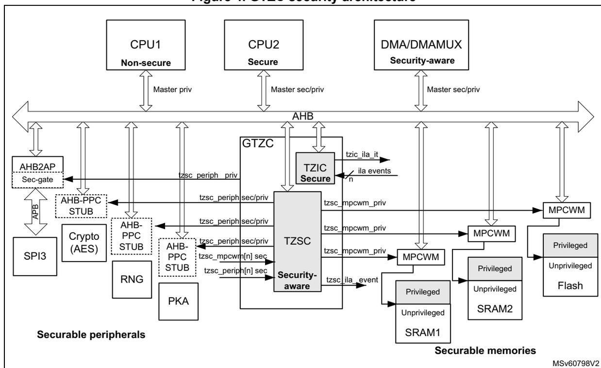
The diagram illustrates the GTZC security architecture. At the top, three main components are shown: CPU1 (Non-secure), CPU2 (Secure), and DMA/DMAMUX (Security-aware). CPU1 is connected to the AHB bus via a 'Master priv' interface. CPU2 and DMA/DMAMUX are connected via 'Master sec/priv' interfaces. The AHB bus is the central communication backbone. Below the bus, several components are connected:
- Securable peripherals: SPI3, Crypto (AES), RNG, PKA, AHB-PPC STUB, and AHB2AP Sec-gate. These are connected to the AHB bus through various interfaces, some labeled with 'tzsc_periph_priv' or 'tzsc_periph_sec/priv'.
- GTZC (Global Security Controller): Consists of two sub-blocks: TZSC (Security-aware) and TZIC (Secure). TZSC is connected to the AHB bus and has multiple output signals: 'tzsc_periph_priv', 'tzsc_periph_sec/priv', 'tzsc_mpcwm_priv', 'tzsc_mpcwm[n] sec', and 'tzsc_periph[n] sec'. TZIC is also connected to the AHB bus and has output signals: 'tzic_ila_it', 'ila events', and 'n'.
- Securable memories: SRAM1, SRAM2, and Flash. SRAM1 and SRAM2 are shown with 'Privileged' and 'Unprivileged' sections. Flash is also shown with 'Privileged' and 'Unprivileged' sections. These are connected to the AHB bus through MPCWM (Memory Protection Controller) blocks. The MPCWM blocks receive signals from TZSC and have output signals like 'tzsc_mpcwm_priv'.
3.4 GTZC functional description
3.4.1 GTZC block diagram
Figure 5 describes the combined feature of TZSC and TZIC. Each sub-block is controlled by its own AHB configuration port. TZSC defines which peripheral is secured and/or privileged. TZIC centralizes the illegal access events.
When the device is non-secure (ESE = 0), TZIC has no function, memories are non-secure and unprivileged and illegal interrupts are disabled. Peripherals can still be made privileged.
Figure 5. GTZC block diagram
![Figure 5. GTZC block diagram. The diagram shows the internal structure of the Global Security Controller (GTZC). It contains two main sub-blocks: TZSC (TrustZone Security Controller) and TZIC (TrustZone Interrupt Controller). The TZSC block includes registers SECCFGR, PRIVCFGGR, and MPCWMR. The TZIC block includes registers IER, MISR, and ICR. External signals include AHB (AHB slaves), ESE (Security enable from user option), tzsc_periph[n]_sec (TZSC peripheral [n] security control from User option), tzsc_mpcwm[n]_sec (TZSC MPCWM [n] security control from User option), n x ila_event (from peripherals), tzsc_periph[n]_sec (output), tzsc_periph[n]_priv (output), tzsc_mpcwm[n]_priv (output), tzsc_ila_event (output), and tzic_ila_it (output). Internal signals include ila_events (input) and tzic_ila_event (output). The diagram is labeled MSV60799V1.](/RM0453-STM32WL5x/2f587210e4f97c32758c5972e2e83d20_img.jpg)
3.4.2 GTZC internal signals
Table 5. GTZC internal signals
| Internal signal name | Signal type | Description |
|---|---|---|
| AHB | Input/output | AHB slaves TZSC and TZIC register access ports |
| ESE | Input | Security enable from user option ESE |
| tzsc_periph[n]_sec | Input | TZSC peripheral [n] security control from User option |
| tzsc_mpcwm[n]_sec | Input | TZSC MPCWM [n] security control from User option |
| tzsc_periph[n]_sec | Output | TZSC peripheral [n] security control |
| tzsc_periph[n]_priv | Output | TZSC peripheral [n] privileged control |
| tzsc_mpcwm[n]_priv | Output | TZSC internal memories MPCWM [n] privileged control |
| tzsc_ila_event | Output | TZSC illegal access event |
| tzic_ila_event | Output | TZIC illegal access event |
| ila_events | Input | Peripheral illegal access events |
| tzic_ila_it | Output | TZIC illegal access interrupt |
3.4.3 Illegal access definition
The existing types of illegal access are listed below:
- • Illegal non-secure read write access
Any non-secure read write transaction trying to access a secure resource is considered as illegal. The addressed resource generates an illegal access event for illegal read /write access.
Note: Some registers have only write security protection and can be accessed read non-secure (refer to individual register descriptions).
- • Illegal unprivileged_read write access
Any unprivileged transaction trying to access a privileged resource is considered as illegal. In all cases, the addressed resource generates an illegal access event for illegal read /write access.
Note: Some registers have only write privileged protection and can be accessed read unprivileged (refer to individual register descriptions).
- • Illegal secure memory fetch access
Any secure_memory fetch access transaction trying to access a non-secure memory resource is considered as illegal. The addressed resource generates an illegal access event and a bus error.
- • Illegal non-secure_memory fetch access
Any non-secure_memory fetch access transaction trying to access a secure memory resource is considered as illegal. The addressed resource generates an illegal access event and a bus error.
- • Illegal unprivileged memory fetch access
Any unprivileged memory fetch access transaction trying to access a privileged memory resource is considered as illegal. The addressed resource generates an illegal access event and a bus error.
- • Peripheral fetch access
Any peripheral fetch access is considered as illegal. The bus bridge generates a bus error for all peripheral fetch access (no illegal access event).
Note: Secure read/write transactions to non-secure memory and peripheral are granted and legal. Privileged read/write transactions to unprivileged memory and peripheral are granted and legal.
Privileged fetch transactions to unprivileged memory are granted and legal.
Table 6. Memory access error generation
| Memory access type (1) | Hide protected memory (HDPADIS = 1) | Secure privileged memory | Secure unprivileged memory | Non-secure privileged memory | Non-secure unprivileged memory | ||||||||||||
|---|---|---|---|---|---|---|---|---|---|---|---|---|---|---|---|---|---|
| Access | lla_event | Bus error | Access | lla_event | Bus error | Access | lla_event | Bus error | Access | lla_event | Bus error | Access | lla_event | Bus error | |||
| Secure | Privileged | Fetch | Illegal | No | Yes | Grant | No | No | Grant | No | No | Illegal | S | Yes | Illegal | S | Yes |
| Read | Yes (2) | Grant | No | No | Grant | No | No | ||||||||||
| Write | No | Illegal | S and P | Yes | Illegal | S | Yes | ||||||||||
| Unprivileged | Fetch | P (3) | Yes | Illegal | P | Yes | |||||||||||
| Read | No | ||||||||||||||||
| Write | No | ||||||||||||||||
| Non-secure | Privileged | Fetch | Illegal | S (4) | Yes | Illegal | S | Yes | Illegal | S | Yes | Grant | No | No | Grant | No | No |
| Read | No | ||||||||||||||||
| Write | No | ||||||||||||||||
| Unprivileged | Fetch | S and P (3/4) | Yes | S and P | Yes | Illegal | P | Yes | |||||||||
| Read | No | ||||||||||||||||
| Write | No | ||||||||||||||||
| Illegal and error event generated | |||||||||||||||||
| Granted | |||||||||||||||||
- 1. Illegal: security infringement
S: lla_event due to illegal security infringement
P: lla_event due to illegal privileged infringement
S and P: lla_event due to secure and privileged infringement - 2. Only for CPU accesses. A DMA access does not generate a bus error.
- 3. When hide protected area is privileged.
- 4. When hide protected area is secure.
Table 7. Peripheral access error generation
| Peripheral access type (1) | Secure privileged peripheral | Secure unprivileged peripheral | Non-secure privileged peripheral | Non-secure unprivileged peripheral | ||||||||||
|---|---|---|---|---|---|---|---|---|---|---|---|---|---|---|
| Access | ila_event | Bus error | Access | ila_event | Bus error | Access | ila_event | Bus error | Access | ila_event | Bus error | |||
| Secure | Privilege | Fetch | Fail | No | Yes | Fail | No | Yes | Fail | No | Yes | Fail | No | Yes |
| Read | Grant | No | Grant | No | Grant | No | Grant | No | ||||||
| Write | Grant | No | Grant | No | Grant | No | Grant | No | ||||||
| Unprivileged | Fetch | Fail | P | Yes | Fail | No | Yes | Illegal | P | Yes | Fail | Yes | ||
| Read | Illegal | No | Grant | No | No | Grant | No | |||||||
| Write | Illegal | No | Grant | No | No | Grant | No | |||||||
| Non-secure | Privilege | Fetch | Fail | No | Yes | Fail | No | Yes | Fail | No | Yes | Fail | No | Yes |
| Read | Illegal | S | No | Illegal | No | Grant | No | Grant | No | |||||
| Write | Illegal | S | No | Illegal | No | Grant | No | Grant | No | |||||
| Unprivileged | Fetch | Fail | No | Yes | Fail | No | Yes | Fail | P | Yes | Fail | Yes | ||
| Read | Illegal | S and P | No | Illegal | S | No | Illegal | No | Grant | No | ||||
| Write | Illegal | S and P | No | Illegal | S | No | Illegal | No | Grant | No | ||||
| Fail, illegal and event generated | ||||||||||||||
| Granted | ||||||||||||||
1. Fail: All fetches from peripherals are rejected without ila generation.
Illegal: security infringement
S: ila_event due to illegal security infringement
P: ila_event due to illegal privileged infringement
S and P: ila_event due to secure and privileged infringement
3.4.4 Security controller (TZSC)
This block is composed of a configurable set of registers, providing the following features:
- Control of secure and privileged protection for peripherals, done through the following registers:
- SECCFGR1 register to control AHB/APB firewall stubs for the secure attribute of all securable peripherals
- PRIVCFGR1 register to control AHB/APB firewall stubs for the privileged attribute of all securable peripherals
- For watermark memory protection (internal memories), one privileged area can be defined through GTZC_TZSC_MPCWMn_UPWMR, that defines the unprivileged area, starting from the internal memory base address with a length defined through GTZC_TZSC_MPCWMn_UPWMR.LGTH[11:0].
- For watermark memory protection (internal memory), one privileged and unprivileged read execute area can be defined through GTZC_TZSC_MPCWM1_UPWWMR, which defines the unprivileged writable area, starting from the internal flash memory base
address with a length defined through GTZC_TZSC_MPCWM1_UPWWMR.LGTH[11:0]. Only the area which is also defined as unprivileged in GTZC_TZSC_MPCWM1_UPWMR.LGTH[11:0] is unprivileged writable.
Note: Where n represents the target memory (1 = Flash memory, 2 = SRAM1 and 3 = SRAM2).
Figure 6. Memory protection control water mark
![Diagram illustrating memory protection control water marks. A vertical axis on the left shows 'Memory base address' at the bottom. Two upward-pointing arrows represent length settings: the outer arrow is labeled UPWMR.LGTH[11:0] and the inner arrow is labeled UPWWMR.LGTH[11:0]. To the right, three horizontal bands represent privilege levels: the top band is 'Privileged', the middle band is 'Privileged and unprivileged read, execute', and the bottom band is 'Unprivileged read, execute and writable'. The diagram shows how the length settings define the memory area for these privilege levels. MSv61500V1 is noted in the bottom right corner.](/RM0453-STM32WL5x/9f51a76cae7309a296cbc6997941eb3f_img.jpg)
3.4.5 Security illegal access controller (TZIC)
This block concentrates all illegal access source events. It is used only when the system is security enabled (ESE = 1). When the system is non-secure (ESE = 0), the generation of an illegal access interrupt is blocked in hardware.
TZIC allows the trace of which event has triggered the illegal interrupt tzic_ila_it . Register masks are available in TZIC_IER to filter unwanted events. Enabled illegal events generate an interrupt to the secure CPU2 NVIC (TZIC_ILA).
For each illegal event source, a status flag and a clear bit exist (respectively within TZIC_MISR and TZIC_ICR registers). The reset value of the enable register TZIC_IER is such that all illegal events are enabled.
3.4.6 Power-on/reset state
The power-on and reset state of TZSC clear all bits of SECCFGR1 and PRIVCFGR1 registers to 0, which respectively means non-secure and unprivileged.
Concerning the internal memories, the reset values of the TZSC MPCWMn_UPWMR and MPCWMn_UPWWMR registers are set to 0x0FFF 0000, making the complete internal memories unprivileged.
CPU1 non-secure privileged boot code can program the non-secure privileged attributes, making components non-secure privileged as needed.
CPU2 secure privileged boot code can program the secure privileged attributes, making components secure privileged as needed.
3.4.7 Interrupts
TZIC is a secure peripheral that generates systematically an illegal access event when accessed by a non-secure access.
TZSC is a security-aware peripheral, meaning that secure and non-secure registers co-exist.
3.5 GTZC TZSC registers
All GTZC TZSC registers are accessed only by words (32-bit). Halfwords (16-bit) and bytes (8-bit) accesses are denied and generate a bus error.
The TZSC MPCWM privileged control registers MPCWMn_UPWMR from the different internal memories are defined in the table below.
Table 8. TZSC privileged MPCWMn register memory allocation
| MPCWM index | Memory | Description |
|---|---|---|
| 1 | Flash | Unprivileged and unprivileged writable control (security controlled by user option) |
| 2 | SRAM1 | Unprivileged control (security controlled by user option) |
| 3 | SRAM2 | Unprivileged control (security controlled by user option) |
3.5.1 GTZC TZSC control register (GTZC_TZSC_CR)
Address offset: 0x000
Reset value: 0x0000 0000
Secure read and write access only
Note: When the system is non-secure (ESE = 0), this register cannot be written and is read zero.
| 31 | 30 | 29 | 28 | 27 | 26 | 25 | 24 | 23 | 22 | 21 | 20 | 19 | 18 | 17 | 16 |
|---|---|---|---|---|---|---|---|---|---|---|---|---|---|---|---|
| Res. | Res. | Res. | Res. | Res. | Res. | Res. | Res. | Res. | Res. | Res. | Res. | Res. | Res. | Res. | Res. |
| 15 | 14 | 13 | 12 | 11 | 10 | 9 | 8 | 7 | 6 | 5 | 4 | 3 | 2 | 1 | 0 |
| Res. | Res. | Res. | Res. | Res. | Res. | Res. | Res. | Res. | Res. | Res. | Res. | Res. | Res. | Res. | LCK |
| rs |
Bits 31:1 Reserved, must be kept at reset value.
Bit 0 LCK : Lock the configuration of TZSC registers until next reset
The configuration is unlocked after a wake-up from Standby.
This bit is unset by default and once set, it cannot be reset until a global TZSC reset.
0: All TZSC registers not locked
1: All TZSC registers locked
3.5.2 GTZC TZSC security configuration register (GTZC_TZSC_SECCFGR1)
Address offset: 0x010
Reset value: 0x0000 0000
Secure write access only.
A bit of this register can be written only by a secure privileged transaction, when the corresponding bit in GTZC_TZSC_PRIVCFGR1 is set to privileged. If unprivileged, the register bit can be written by secure privileged and secure unprivileged transactions.
Read access is authorized for any type of transaction, secure/non-secure, privileged/unprivileged.
An illegal access event on a privileged access is only generated when all peripheral register bits in GTZC_TZSC_PRIVCFGR1 are configured as privileged.
When TZSC configuration is locked in GTZC_TZSC_CR.LCK, this register can no longer be modified.
Note: When the system is non-secure (ESE = 0) this register cannot be written and is read zero. Peripherals cannot be secured.
| 31 | 30 | 29 | 28 | 27 | 26 | 25 | 24 | 23 | 22 | 21 | 20 | 19 | 18 | 17 | 16 |
|---|---|---|---|---|---|---|---|---|---|---|---|---|---|---|---|
| Res. | Res. | Res. | Res. | Res. | Res. | Res. | Res. | Res. | Res. | Res. | Res. | Res. | Res. | Res. | Res. |
| 15 | 14 | 13 | 12 | 11 | 10 | 9 | 8 | 7 | 6 | 5 | 4 | 3 | 2 | 1 | 0 |
| Res. | Res. | PKA SEC | Res. | Res. | Res. | Res. | Res. | Res. | Res. | Res. | Res. | RNG SEC | AES SEC | Res. | Res. |
| rw | rw | rw |
Bits 31:14 Reserved, must be kept at reset value.
Bit 13 PKASEC : Secure access mode enabled for PKA
0: Non-secure
1: Secure
Bits 12:4 Reserved, must be kept at reset value.
Bit 3 RNGSEC : Secure access mode enabled for RNG
0: Non-secure
1: Secure
Bit 2 AESSEC : Secure access mode enabled for AES
0: Non-secure
1: Secure
Bits 1:0 Reserved, must be kept at reset value.
3.5.3 GTZC TZSC privileged configuration register (GTZC_TZSC_PRIVCFGR1)
Address offset: 0x020
Reset value: 0x0000 0000
Privileged write access only.
A bit of this register can be written only by a secure privileged transaction, when the corresponding bit in GTZC_TZSC_SECCFGR1 register or the flash user option is set to secure. If non-secure, the register bit can be written by secure privileged and non-secure privileged transactions.
Read access is authorized for any type of transaction, secure/non-secure, privileged/unprivileged.
An illegal access event on a secure access is only generated when all peripheral register bits in GTZC_TZSC_SECCFGR1 are configured as secure.
When TZSC configuration is locked in GTZC_TZSC_CR.LCK, this register cannot be modified.
| 31 | 30 | 29 | 28 | 27 | 26 | 25 | 24 | 23 | 22 | 21 | 20 | 19 | 18 | 17 | 16 |
|---|---|---|---|---|---|---|---|---|---|---|---|---|---|---|---|
| Res. | Res. | Res. | Res. | Res. | Res. | Res. | Res. | Res. | Res. | Res. | Res. | Res. | Res. | Res. | Res. |
| 15 | 14 | 13 | 12 | 11 | 10 | 9 | 8 | 7 | 6 | 5 | 4 | 3 | 2 | 1 | 0 |
| Res. | Res. | PKAPRIV | Res. | Res. | Res. | Res. | Res. | Res. | Res. | Res. | SUBGHZSPIPRIV | RNGPRIV | AESPRIV | Res. | Res. |
| rw | rw | rw | rw |
Bits 31:14 Reserved, must be kept at reset value.
Bit 13 PKAPRIV : Privileged access mode enabled for PKA
0: Unprivileged
1: Privileged
Bits 12:5 Reserved, must be kept at reset value.
Bit 4 SUBGHZSPIPRIV : Privileged access mode enabled for sub-GHz SPI
0: Unprivileged
1: Privileged
Bit 3 RNGPRIV : Privileged access mode enabled for RNG
0: Unprivileged
1: Privileged
Bit 2 AESPRIV : Privileged access mode enabled for AES
0: Unprivileged
1: Privileged
Bits 1:0 Reserved, must be kept at reset value.
3.5.4 GTZC TZSC unprivileged watermark 1 register (GTZC_TZSC_MPCWM1_UPWMR)
Address offset: 0x130
Reset value: 0x0FFF 0000
Privileged write access only.
This register can be written only by secure privileged transaction, when the corresponding flash user option FSD is configured as secure. If non-secure, this register can be written by secure privileged and non-secure privileged transaction.
Read access is authorized for any type of transaction, secure/non-secure, privileged/unprivileged.
When TZSC configuration is locked in GTZC_TZSC_CR.LCK, this register cannot be modified.
Note: When the system is non-secure (ESE = 0), this register can be written and read, however bits have no function.
| 31 | 30 | 29 | 28 | 27 | 26 | 25 | 24 | 23 | 22 | 21 | 20 | 19 | 18 | 17 | 16 |
|---|---|---|---|---|---|---|---|---|---|---|---|---|---|---|---|
| Res. | Res. | Res. | Res. | LGTH[11:0] | |||||||||||
| rw | rw | rw | rw | rw | rw | rw | rw | rw | rw | rw | rw | ||||
| 15 | 14 | 13 | 12 | 11 | 10 | 9 | 8 | 7 | 6 | 5 | 4 | 3 | 2 | 1 | 0 |
| Res. | Res. | Res. | Res. | Res. | Res. | Res. | Res. | Res. | Res. | Res. | Res. | Res. | Res. | Res. | Res. |
Bits 31:28 Reserved, must be kept at reset value.
Bits 27:16 LGTH[11:0] : Define the length of user flash unprivileged area (in 2-Kbyte resolution, starting from the user flash base address)
Note: This register has only effect when security is enabled (ESE = 1). When security is disabled, the memory is completely unprivileged, whatever the value.
0x000: No unprivileged area, privileged 0x00000 to 0x3FFFF
0x001: Unprivileged 0x00000 to 0x007FF, privileged 0x00800 to 0x3FFFF
0x002: Unprivileged 0x00000 to 0x00FFF, privileged 0x01000 to 0x3FFFF
0x003: Unprivileged 0x00000 to 0x017FF, privileged 0x01800 to 0x3FFFF
.....
0x080 and greater: Unprivileged 0x00000 to 0x3FFFF, no privileged area
Note: 0x800 and greater are truncated to 0x800.
Bits 15:0 Reserved, must be kept at reset value.
3.5.5 GTZC TZSC unprivileged writable watermark 1 register (GTZC_TZSC_MPCWM1_UPWWMR)
Address offset: 0x134
Reset value: 0x0FFF 0000
Privileged write access only.
This register can be written only by secure privileged transaction when the corresponding flash user option FSD is configured as secure. If non-secure, this register can be written by secure privileged and non-secure privileged transaction.
Read access is authorized for any type of transaction, secure/non-secure, privileged/unprivileged.
When TZSC configuration is locked in GTZC_TZSC_CR.LCK, this register cannot be modified.
Note: When the system is non-secure (ESE = 0), this register can be written and read, however bits have no function.
| 31 | 30 | 29 | 28 | 27 | 26 | 25 | 24 | 23 | 22 | 21 | 20 | 19 | 18 | 17 | 16 |
|---|---|---|---|---|---|---|---|---|---|---|---|---|---|---|---|
| Res. | Res. | Res. | Res. | LGTH[11:0] | |||||||||||
| rw | rw | rw | rw | rw | rw | rw | rw | rw | rw | rw | rw | ||||
| 15 | 14 | 13 | 12 | 11 | 10 | 9 | 8 | 7 | 6 | 5 | 4 | 3 | 2 | 1 | 0 |
| Res. | Res. | Res. | Res. | Res. | Res. | Res. | Res. | Res. | Res. | Res. | Res. | Res. | Res. | Res. | Res. |
Bits 31:28 Reserved, must be kept at reset value.
Bits 27:16 LGTH[11:0] : Define the length of flash unprivileged writable area (in 2-Kbyte resolution, starting from the user flash base address)
Only the area which is also defined as unprivileged in
GTZC_TZSC_MPCWM1_UPWMR.LGTH[11:0] is unprivileged writable.
Note: This register has only effect when security is enabled (ESE = 1). When security is disabled, the memory is completely unprivileged writable, whatever the value.
0x000: No unprivileged writable area, privileged and unprivileged read execute 0x00000 to 0x3FFFF
0x001: Unprivileged writable 0x00000 to 0x007FF, privileged and unprivileged read execute 0x00800 to 0x3FFFF
0x002: Unprivileged writable 0x00000 to 0x00FFF, privileged and unprivileged read execute 0x01000 to 0x3FFFF
0x003: Unprivileged writable 0x00000 to 0x017FF, privileged and unprivileged read execute 0x01800 to 0x3FFFF
.....
0x080 and greater: Unprivileged writable 0x00000 to 0x3FFFF, no privileged and unprivileged read execute area
Note: 0x800 and greater are truncated to 0x800
Bits 15:0 Reserved, must be kept at reset value.
3.5.6 GTZC TZSC unprivileged watermark 2 register (GTZC_TZSC_MPCWM2_UPWMR)
Address offset: 0x138
Reset value: 0x0FFF 0000
Privileged write access only.
This register can be written only by secure privileged transaction, when the corresponding flash user option NBRSD is configured as secure. If non-secure, this register can be written by secure privileged and non-secure privileged transaction.
Read access is authorized for any type of transaction, secure/non-secure, privileged/unprivileged.
When TZSC configuration is locked in GTZC_TZSC_CR.LCK, this register cannot be modified.
Note: When the system is non-secure (ESE = 0), this register can be written and read, however bits have no function.
| 31 | 30 | 29 | 28 | 27 | 26 | 25 | 24 | 23 | 22 | 21 | 20 | 19 | 18 | 17 | 16 |
|---|---|---|---|---|---|---|---|---|---|---|---|---|---|---|---|
| Res. | Res. | Res. | Res. | LGTH[11:0] | |||||||||||
| rw | rw | rw | rw | rw | rw | rw | rw | rw | rw | rw | rw | ||||
| 15 | 14 | 13 | 12 | 11 | 10 | 9 | 8 | 7 | 6 | 5 | 4 | 3 | 2 | 1 | 0 |
| Res. | Res. | Res. | Res. | Res. | Res. | Res. | Res. | Res. | Res. | Res. | Res. | Res. | Res. | Res. | Res. |
Bits 31:28 Reserved, must be kept at reset value.
Bits 27:16 LGTH[11:0] : Define the length of SRAM1 unprivileged area (in 1-Kbyte resolution, starting from the SRAM1 base address)
Note: This register has only effect when security is enabled (ESE = 1). When security is disabled, the memory is completely unprivileged, whatever the value.
0x000: No unprivileged area, privileged 0x0000 to 0x7FFF
0x001: Unprivileged 0x0000 to 0x03FF, privileged 0x0400 to 0x7FFF
0x002: Unprivileged 0x0000 to 0x07FF, privileged 0x0800 to 0x7FFF
0x003: Unprivileged 0x0000 to 0x0BFF, privileged 0x0C00 to 0x7FFF
.....
0x020 and greater: Unprivileged 0x0000 to 0x7FFF, no privileged area
Note: 0x800 and greater are truncated to 0x800
Bits 15:0 Reserved, must be kept at reset value.
3.5.7 GTZC TZSC unprivileged watermark 3 register (GTZC_TZSC_MPCWM3_UPWMR)
Address offset: 0x140
Reset value: 0x0FFF 0000
Privileged write access only.
This register can be written only by secure privileged transaction, when the corresponding flash user option BRSD is configured as secure. If non-secure, this register can be written by secure privileged and non-secure privileged transaction.
Read access is authorized for any type of transaction, secure/non-secure, privileged/unprivileged.
When TZSC configuration is locked in GTZC_TZSC_CR.LCK, this register cannot be modified.
Note: When the system is non-secure (ESE = 0), this register can be written and read, however bits have no function.
| 31 | 30 | 29 | 28 | 27 | 26 | 25 | 24 | 23 | 22 | 21 | 20 | 19 | 18 | 17 | 16 |
|---|---|---|---|---|---|---|---|---|---|---|---|---|---|---|---|
| Res. | Res. | Res. | Res. | LGTH[11:0] | |||||||||||
| rw | rw | rw | rw | rw | rw | rw | rw | rw | rw | rw | rw | ||||
| 15 | 14 | 13 | 12 | 11 | 10 | 9 | 8 | 7 | 6 | 5 | 4 | 3 | 2 | 1 | 0 |
| Res. | Res. | Res. | Res. | Res. | Res. | Res. | Res. | Res. | Res. | Res. | Res. | Res. | Res. | Res. | Res. |
Bits 31:28 Reserved, must be kept at reset value.
Bits 27:16 LGTH[11:0] : Define the length of SRAM2 unprivileged area (in 1-Kbyte resolution, starting from the SRAM2 base address)
Note: This register has only effect when security is enabled (ESE = 1). When security is disabled, the memory is completely unprivileged, whatever the value.
0x000: No unprivileged area, privileged 0x0000 to 0x7FFF
0x001: Unprivileged 0x0000 to 0x03FF, privileged 0x0400 to 0x7FFF
0x002: Unprivileged 0x0000 to 0x07FF, privileged 0x0800 to 0x7FFF
0x003: Unprivileged 0x0000 to 0x0BFF, privileged 0x0C00 to 0x7FFF
.....
0x020 and greater: Unprivileged 0x0000 to 0x7FFF, no privileged area
Note: 0x800 and greater are truncated to 0x800
Bits 15:0 Reserved, must be kept at reset value.
3.5.8 GTZC TZSC register map
Table 9. GTZC TZSC register map and reset values
| Offset | Register | 31 | 30 | 29 | 28 | 27 | 26 | 25 | 24 | 23 | 22 | 21 | 20 | 19 | 18 | 17 | 16 | 15 | 14 | 13 | 12 | 11 | 10 | 9 | 8 | 7 | 6 | 5 | 4 | 3 | 2 | 1 | 0 |
|---|---|---|---|---|---|---|---|---|---|---|---|---|---|---|---|---|---|---|---|---|---|---|---|---|---|---|---|---|---|---|---|---|---|
| 0x000 | GTZC_TZSC_CR | Res. | Res. | Res. | Res. | Res. | Res. | Res. | Res. | Res. | Res. | Res. | Res. | Res. | Res. | Res. | Res. | Res. | Res. | Res. | Res. | Res. | Res. | Res. | Res. | Res. | Res. | Res. | Res. | Res. | Res. | Res. | LCK |
| Reset value | 0 | ||||||||||||||||||||||||||||||||
| 0x004 to 0x00C | Reserved | Reserved | |||||||||||||||||||||||||||||||
| 0x010 | GTZC_TZSC_SECCFGGR1 | Res. | Res. | Res. | Res. | Res. | Res. | Res. | Res. | Res. | Res. | Res. | Res. | Res. | Res. | Res. | Res. | Res. | Res. | PKASEC | Res. | Res. | Res. | Res. | Res. | Res. | Res. | Res. | Res. | Res. | RNGSEC | AESSEC | Res. |
| Reset value | 0 | 0 | 0 | ||||||||||||||||||||||||||||||
| 0x014 to 0x01C | Reserved | Reserved | |||||||||||||||||||||||||||||||
| 0x020 | GTZC_TZSC_PRIVCFGGR1 | Res. | Res. | Res. | Res. | Res. | Res. | Res. | Res. | Res. | Res. | Res. | Res. | Res. | Res. | Res. | Res. | Res. | Res. | PKAPRIV | Res. | Res. | Res. | Res. | Res. | Res. | Res. | Res. | Res. | SUBGHZSPIPRIV | RNGPRIV | AESPRIV | Res. |
| Reset value | 0 | 0 | 0 | 0 | |||||||||||||||||||||||||||||
| 0x024 to 0x12C | Reserved | Reserved | |||||||||||||||||||||||||||||||
| 0x130 | GTZC_TZSC_MPCWM1_UPWMR | Res. | Res. | Res. | Res. | LGTH[11:0] | Res. | Res. | Res. | Res. | Res. | Res. | Res. | Res. | Res. | Res. | Res. | Res. | Res. | Res. | Res. | Res. | |||||||||||
| Reset value | 1 | 1 | 1 | 1 | 1 | 1 | 1 | 1 | 1 | 1 | 1 | 1 | |||||||||||||||||||||
| 0x134 | GTZC_TZSC_MPCWM1_UPWMR | Res. | Res. | Res. | Res. | LGTH[11:0] | Res. | Res. | Res. | Res. | Res. | Res. | Res. | Res. | Res. | Res. | Res. | Res. | Res. | Res. | Res. | Res. | |||||||||||
| Reset value | 1 | 1 | 1 | 1 | 1 | 1 | 1 | 1 | 1 | 1 | 1 | 1 | |||||||||||||||||||||
| 0x138 | GTZC_TZSC_MPCWM2_UPWMR | Res. | Res. | Res. | Res. | LGTH[11:0] | Res. | Res. | Res. | Res. | Res. | Res. | Res. | Res. | Res. | Res. | Res. | Res. | Res. | Res. | Res. | Res. | |||||||||||
| Reset value | 1 | 1 | 1 | 1 | 1 | 1 | 1 | 1 | 1 | 1 | 1 | 1 | |||||||||||||||||||||
| 0x13C | Reserved | Reserved | |||||||||||||||||||||||||||||||
| 0x140 | GTZC_TZSC_MPCWM3_UPWMR | Res. | Res. | Res. | Res. | LGTH[11:0] | Res. | Res. | Res. | Res. | Res. | Res. | Res. | Res. | Res. | Res. | Res. | Res. | Res. | Res. | Res. | Res. | |||||||||||
| Reset value | 1 | 1 | 1 | 1 | 1 | 1 | 1 | 1 | 1 | 1 | 1 | 1 | |||||||||||||||||||||
Refer to Section 2.6 for the register boundary addresses.
3.6 GTZC TZIC registers
All GTZC TZIC registers are accessed by words (32-bit), halfwords (16-bit) and bytes (8-bit).
3.6.1 GTZC TZIC interrupt enable register 1 (GTZC_TZIC_IER1)
Address offset: 0x000
Reset value: 0xFFFF FFFF
when security is enabled (ESE = 1)
Reset value: 0x0000 0000
when security is disabled (ESE = 0)
This register can only be accessed by a secure privileged access for read and write.
A non-secure or unprivileged access is ignored and return zero data, and an illegal access event is generated.
Note: When the system is non-secure (ESE = 0), this register cannot be written and is read zero. No illegal access interrupt is generated.
| 31 | 30 | 29 | 28 | 27 | 26 | 25 | 24 | 23 | 22 | 21 | 20 | 19 | 18 | 17 | 16 |
|---|---|---|---|---|---|---|---|---|---|---|---|---|---|---|---|
| Res. | Res. | Res. | Res. | Res. | Res. | Res. | Res. | Res. | Res. | Res. | Res. | Res. | Res. | Res. | Res. |
| 15 | 14 | 13 | 12 | 11 | 10 | 9 | 8 | 7 | 6 | 5 | 4 | 3 | 2 | 1 | 0 |
| Res. | Res. | PKAIE | SRAM2 IE | SRAM1 IE | FLASH IE | DMAMUX1IE | DMA2 IE | DMA1 IE | FLASH IFIE | PWRIE | SUBG HZSP IIE | RNGIE | AESIE | TZSC IE | TZICIE |
| rw | rw | rw | rw | rw | rw | rw | rw | rw | rw | rw | rw | rw | rw |
Bits 31:14 Reserved, must be kept at reset value.
Bit 13 PKAIE : Illegal access event interrupt enable bit for PKA
- 0: Disabled (masked)
- 1: Enabled (unmasked)
Bit 12 SRAM2IE : Illegal access event interrupt enable bit for SRAM2
- 0: Disabled (masked)
- 1: Enabled (unmasked)
Bit 11 SRAM1IE : Illegal access event interrupt enable bit for SRAM1
- 0: Disabled (masked)
- 1: Enabled (unmasked)
Bit 10 FLASHIE : Illegal access event interrupt enable bit for flash memory
- 0: Disabled (masked)
- 1: Enabled (unmasked)
Bit 9 DMAMUX1IE : Illegal access event interrupt enable bit for DMAMUX1
- 0: Disabled (masked)
- 1: Enabled (unmasked)
Bit 8 DMA2IE : Illegal access event interrupt enable bit for DMA2
- 0: Disabled (masked)
- 1: Enabled (unmasked)
- Bit 7
DMA1IE
: Illegal access event interrupt enable bit for DMA1
0: Disabled (masked)
1: Enabled (unmasked) - Bit 6
FLASHIE
: Illegal access event interrupt enable bit for FLASH interface
0: Disabled (masked)
1: Enabled (unmasked) - Bit 5
PWRIE
: Illegal access event interrupt enable bit for PWR
0: Disabled (masked)
1: Enabled (unmasked) - Bit 4
SUBGHZSPIE
: Illegal access event interrupt enable bit for sub-GHz SPI
0: Disabled (masked)
1: Enabled (unmasked) - Bit 3
RNGIE
: Illegal access event interrupt enable bit for RNG
0: Disabled (masked)
1: Enabled (unmasked) - Bit 2
AESIE
: Illegal access event interrupt enable bit for AES
0: Disabled (masked)
1: Enabled (unmasked) - Bit 1
TZSCIE
: Illegal access event interrupt enable bit for GTZC TZSC
0: Disabled (masked)
1: Enabled (unmasked) - Bit 0
TZICIE
: Illegal access event interrupt enable bit for GTZC TZIC
0: Disabled (masked)
1: Enabled (unmasked)
3.6.2 GTZC TZIC status register 1 (GTZC_TZIC_MISR1)
Address offset: 0x010
Reset value: 0x0000 0000
This register can only be accessed by a secure privileged access for read and write. A non-secure or unprivileged access is ignored and return zero data and an illegal access event is generated.
Note: When the system is non-secure (ESE = 0) this register cannot be written and reads zero.
| 31 | 30 | 29 | 28 | 27 | 26 | 25 | 24 | 23 | 22 | 21 | 20 | 19 | 18 | 17 | 16 |
|---|---|---|---|---|---|---|---|---|---|---|---|---|---|---|---|
| Res. | Res. | Res. | Res. | Res. | Res. | Res. | Res. | Res. | Res. | Res. | Res. | Res. | Res. | Res. | Res. |
| 15 | 14 | 13 | 12 | 11 | 10 | 9 | 8 | 7 | 6 | 5 | 4 | 3 | 2 | 1 | 0 |
| Res. | Res. | PKAMF | SRAM2 MF | SRAM1 MF | FLASH MF | DMAM UX1MF | DMA2 MF | DMA1 MF | FLASHI FMF | PWR MF | SUBG HZSPI MF | RNG MF | AESMF | TZSC MF | TZIC MF |
| r | r | r | r | r | r | r | r | r | r | r | r | r | r |
Bits 31:14 Reserved, must be kept at reset value.
- Bit 13
PKAMF
: Illegal access event interrupt status flag before masking for PKA
0: No illegal access event interrupt pending
1: Illegal access event interrupt pending - Bit 12
SRAM2MF
: Illegal access event interrupt status flag before masking for SRAM2
0: No illegal access event interrupt pending
1: Illegal access event interrupt pending - Bit 11
SRAM1MF
: Illegal access event interrupt status flag before masking for SRAM1
0: No illegal access event interrupt pending
1: Illegal access event interrupt pending - Bit 10
FLASHMF
: Illegal access event interrupt status flag before masking for flash memory
0: No illegal access event interrupt pending
1: Illegal access event interrupt pending - Bit 9
DMAMUX1MF
: Illegal access event interrupt status flag before masking for DMAMUX1
0: No illegal access event interrupt pending
1: Illegal access event interrupt pending. - Bit 8
DMA2MF
: Illegal access event interrupt status flag before masking for DMA2
0: No illegal access event interrupt pending
1: Illegal access event interrupt pending - Bit 7
DMA1MF
: Illegal access event interrupt status flag before masking for DMA1
0: No illegal access event interrupt pending
1: Illegal access event interrupt pending - Bit 6
FLASHIFMF
: Illegal access event interrupt status flag before masking for flash interface
0: No illegal access event interrupt pending
1: Illegal access event interrupt pending - Bit 5
PWRMF
: Illegal access event interrupt status flag before masking for PWR
0: No illegal access event interrupt pending
1: Illegal access event interrupt pending - Bit 4
SUBGHZSPIMF
: Illegal access event interrupt status flag before masking for sub-GHz SPI
0: No illegal access event interrupt pending
1: Illegal access event interrupt pending - Bit 3
RNGMF
: Illegal access event interrupt status flag before masking for RNG
0: No illegal access event interrupt pending
1: Illegal access event interrupt pending - Bit 2
AESMF
: Illegal access event interrupt status flag before masking for AES
0: No illegal access event interrupt pending
1: Illegal access event interrupt pending - Bit 1
TZSCMF
: Illegal access event interrupt status flag before masking for GTZC TZSC
0: No illegal access event interrupt pending
1: Illegal access event interrupt pending - Bit 0
TZICMF
: Illegal access event interrupt status flag before masking for GTZC TZIC
0: No illegal access event interrupt pending
1: Illegal access event interrupt pending
3.6.3 GTZC TZIC interrupt status clear register 1 (GTZC_TZIC_ICR1)
Address offset: 0x020
Reset value: 0x0000 0000
This register can only be accessed by a secure privileged access for read and write. A non-secure or unprivileged access is ignored and return zero data and an illegal access event is generated.
Note: When the system is non-secure (ESE = 0), this register cannot be written and reads zero.
| 31 | 30 | 29 | 28 | 27 | 26 | 25 | 24 | 23 | 22 | 21 | 20 | 19 | 18 | 17 | 16 |
|---|---|---|---|---|---|---|---|---|---|---|---|---|---|---|---|
| Res. | Res. | Res. | Res. | Res. | Res. | Res. | Res. | Res. | Res. | Res. | Res. | Res. | Res. | Res. | Res. |
| 15 | 14 | 13 | 12 | 11 | 10 | 9 | 8 | 7 | 6 | 5 | 4 | 3 | 2 | 1 | 0 |
| Res. | Res. | PKACF | SRAM2 CF | SRAM1 CF | FLASH CF | DMAMUX1CF | DMA2 CF | DMA1 CF | FLASHI FCF | PWR CF | SUBG HZSPI CF | RNG CF | AESCF | TZSC CF | TZIC CF |
| rc_w1 | rc_w1 | rc_w1 | rc_w1 | rc_w1 | rc_w1 | rc_w1 | rc_w1 | rc_w1 | rc_w1 | rc_w1 | rc_w1 | rc_w1 | rc_w1 |
Bits 31:14 Reserved, must be kept at reset value.
Bit 13 PKACF : Illegal access event interrupt status flag clear bit for PKA
0: No action
1: Clear status flag
Bit 12 SRAM2CF : Illegal access event interrupt status flag clear bit for SRAM2
0: No action
1: Clear status flag
Bit 11 SRAM1CF : Illegal access event interrupt status flag clear bit for SRAM1
0: No action
1: Clear status flag
Bit 10 FLASHCF : Illegal access event interrupt status flag clear bit for flash memory
0: No action
1: Clear status flag
Bit 9 DMAMUX1CF : Illegal access event interrupt status flag clear bit for DMAMUX1
0: No action
1: Clear status flag
Bit 8 DMA2CF : Illegal access event interrupt status flag clear bit for DMA2
0: No action
1: Clear status flag
Bit 7 DMA1CF : Illegal access event interrupt status flag clear bit for DMA1
0: No action
1: Clear status flag
Bit 6 FLASHIFCF : Illegal access event interrupt status flag clear bit for flash interface
0: No action
1: Clear status flag
Bit 5 PWRCF : Illegal access event interrupt status flag clear bit for PWR
0: No action
1: Clear status flag
Bit 4 SUBGHZSPICF : Illegal access event interrupt status flag clear bit for sub-GHz SPI
0: No action
1: Clear status flag
Bit 3 RNGCF : Illegal access event interrupt status flag clear bit for RNG
0: No action
1: Clear status flag
Bit 2 AESCF : Illegal access event interrupt status flag clear bit for AES
0: No action
1: Clear status flag
Bit 1 TZSCCF : Illegal access event interrupt status flag clear bit for GTZC TZSC
0: No action
1: Clear status flag
Bit 0 TZICCF : Illegal access event interrupt status flag clear bit for GTZC TZIC
0: No action
1: Clear status flag
3.6.4 GTZC TZIC register map
Table 10. TZIC register map and reset values
| Offset | Register | 31 | 30 | 29 | 28 | 27 | 26 | 25 | 24 | 23 | 22 | 21 | 20 | 19 | 18 | 17 | 16 | 15 | 14 | 13 | 12 | 11 | 10 | 9 | 8 | 7 | 6 | 5 | 4 | 3 | 2 | 1 | 0 |
|---|---|---|---|---|---|---|---|---|---|---|---|---|---|---|---|---|---|---|---|---|---|---|---|---|---|---|---|---|---|---|---|---|---|
| 0x000 | GTZC_TZIC_IER1 | Res. | Res. | Res. | Res. | Res. | Res. | Res. | Res. | Res. | Res. | Res. | Res. | Res. | Res. | Res. | Res. | Res. | Res. | PKAIE | SRAM2IE | SRAM1IE | FLASHIE | DMAMUX1IE | DMA2IE | DMA1IE | FLASHFIE | PWRIE | SUBGHZSPIE | RNGIE | AESIE | TZSCIE | TZICIE |
| Reset value | x | x | x | x | x | x | x | x | x | x | x | x | x | x | |||||||||||||||||||
| 0x004 to 0x00C | Reserved | Reserved | |||||||||||||||||||||||||||||||
| 0x010 | GTZC_TZIC_MISR1 | Res. | Res. | Res. | Res. | Res. | Res. | Res. | Res. | Res. | Res. | Res. | Res. | Res. | Res. | Res. | Res. | Res. | Res. | PKAMF | SRAM2MF | SRAM1MF | FLASHMF | DMAMUX1MF | DMA2MF | DMA1MF | FLASHIFMF | PWRMF | SUBGHZSPIMF | RNGMF | AESMF | TZSCMF | TZICMF |
| Reset value | 0 | 0 | 0 | 0 | 0 | 0 | 0 | 0 | 0 | 0 | 0 | 0 | 0 | 0 | |||||||||||||||||||
| 0x014 to 0x01C | Reserved | Reserved | |||||||||||||||||||||||||||||||
| 0x020 | GTZC_TZIC_ICR1 | Res. | Res. | Res. | Res. | Res. | Res. | Res. | Res. | Res. | Res. | Res. | Res. | Res. | Res. | Res. | Res. | Res. | Res. | PKACF | SRAM2CF | SRAM1CF | FLASHCF | DMAMUX1CF | DMA2CF | DMA1CF | FLASHIFCF | PWRCF | SUBGHZSPICF | RNGCF | AESCF | TZSCF | TZICF |
| Reset value | 0 | 0 | 0 | 0 | 0 | 0 | 0 | 0 | 0 | 0 | 0 | 0 | 0 | 0 | |||||||||||||||||||
Refer to Section 2.6 for the register boundary addresses.