2. Memory and bus architecture
The following definitions are used in this section:
- • CPU1 = Arm Cortex-M4 with MPU and DSP
- • CPU2 = Arm Cortex-M0+ with MPU
When ESE = 0, CPU2 is non-secure. When ESE = 1, CPU2 is secure.
2.1 System architecture
The main system consists of a 32-bit multilayer AHB bus matrix that interconnects the following masters and slaves:
- • Six masters:
- – CPU1 core I-bus
- – CPU1 core D-bus
- – CPU1 core S-bus
- – CPU2 core S-bus
- – DMA1
- – DMA2
- • Eight slaves:
- – Internal flash memory on the CPU1 Code bus
- – Internal flash memory on CPU1 DCode bus
- – Internal flash memory on CPU2 S bus
- – Internal SRAM1 (32 Kbytes)
- – Internal SRAM2 (32 Kbytes)
- – AHB1 peripherals including AHB to APB bridges and APB peripherals (connected to APB1 and APB2)
- – AHB2 peripherals
- – AHB3 peripherals including AHB to APB bridges and APB peripherals (connected to APB3)
The bus matrix provides access from a master to a slave, enabling concurrent access and efficient operation even when several high-speed peripherals work simultaneously.
This architecture is shown in the figure below.
Figure 1. System architecture
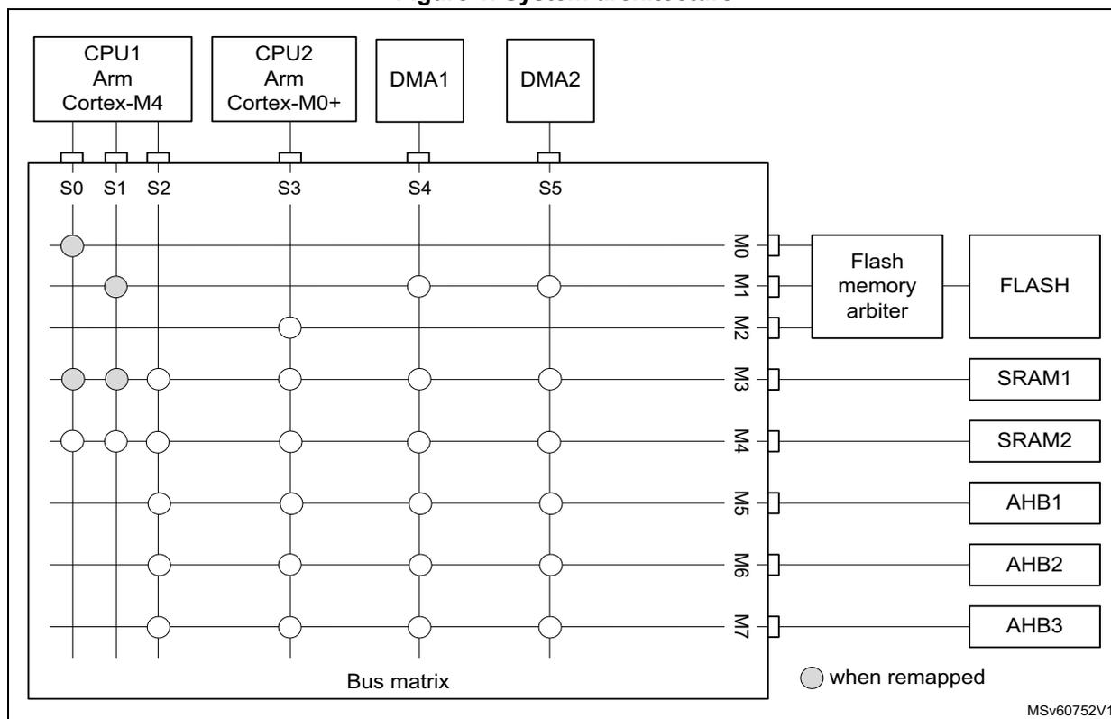
The diagram illustrates the system architecture based on a bus matrix. At the top, four components are shown: CPU1 (Arm Cortex-M4), CPU2 (Arm Cortex-M0+), DMA1, and DMA2. These are connected to a central 'Bus matrix' through source ports S0, S1, S2, S3, S4, and S5. The bus matrix has eight target ports labeled M0 through M7. The connections are as follows:
- S0 (CPU1 I-bus): Connects to M0 (when remapped), M2, M3, and M4.
- S1 (CPU1 D-bus): Connects to M0 (when remapped), M1 (when remapped), M2, M3, and M4.
- S2 (CPU1 S-bus): Connects to M1 (when remapped), M2, M3, M4, M5, M6, and M7.
- S3 (CPU2 S-bus): Connects to M2, M3, M4, M5, M6, and M7.
- S4 (DMA1): Connects to M1 (when remapped), M3, M4, M5, M6, and M7.
- S5 (DMA2): Connects to M1 (when remapped), M3, M4, M5, M6, and M7.
The target ports are connected to the following components:
- M0: Flash memory arbiter (when remapped).
- M1: FLASH (when remapped).
- M2: FLASH, SRAM1, and SRAM2.
- M3: FLASH, SRAM1, SRAM2, and AHB1.
- M4: FLASH, SRAM1, SRAM2, AHB1, and AHB2.
- M5: FLASH, SRAM1, SRAM2, AHB1, AHB2, and AHB3.
- M6: FLASH, SRAM1, SRAM2, AHB1, AHB2, and AHB3.
- M7: FLASH, SRAM1, SRAM2, AHB1, AHB2, and AHB3.
A legend indicates that a grey circle represents a connection 'when remapped'. The diagram is labeled MSv60752V1.
2.1.1 S0: CPU1 I-bus
This bus connects the instruction bus of the CPU1 core to the bus matrix. This bus is used by the core to fetch instructions. The targets of this bus are the internal flash memory, SRAM1 and SRAM2.
2.1.2 S1: CPU1 D-bus
This bus connects the data bus of the CPU1 core to the bus matrix. This bus is used by the core for literal load and debug access. The targets of this bus are the internal flash memory, SRAM1 and SRAM2.
2.1.3 S2: CPU1 S-bus
This bus connects the system bus of the CPU1 core to the bus matrix. This bus is used by the core to access data located in a peripheral or SRAM area. The targets of this bus are the SRAM1, SRAM2, the AHB1 peripherals including the APB1 and APB2 peripherals, the AHB2 peripherals and the AHB3 peripherals including the APB3.
2.1.4 S3: CPU2 S-bus
This bus connects the system bus of the CPU2 core to the bus matrix. This bus is used by the core to fetch instructions, for literal load and debug access, and access data located in a peripheral or SRAM area. The targets of this bus are the internal flash memory, SRAM1,
SRAM2, the AHB1 peripherals including the APB1 and APB2 peripherals, the AHB2 peripherals and the AHB3 peripherals including the APB3 peripherals.
2.1.5 S4, S5: DMA-bus
These buses connect the AHB master interface of the DMAs to the bus matrix. The targets of this bus are the internal flash memory, SRAM1, SRAM2 the AHB1 peripherals including the APB1 and APB2 peripherals, the AHB2 peripherals and the AHB3 peripherals including the APB3 peripherals.
AHB/APB bridges
The two bridges AHB to APB1 and AHB to APB2 provide full synchronous connections between the AHB1 and the two APB buses, allowing flexible selection of the peripheral frequency.
The bridge AHB to APB3 provides full synchronous connections between the AHB and the APB bus, allowing flexible selection of the frequency between the AHB and peripherals.
Refer to Section 2.6.2: Memory map and register boundary addresses for the address mapping of the peripherals connected to this bridge.
After each device reset, all peripheral clocks are disabled, except for the SRAM1/2 and the flash memory interface. Before using a peripheral, its clock must be enabled in the RCC_AHBxENR and RCC_APBxENR registers.
Note: When a 16- or 8-bit access is performed on an APB register, the access is transformed into a 32-bit access: the bridge duplicates the 16- or 8-bit data to feed the 32-bit vector.
2.2 Boot configuration
Three different CPU1 boot modes and one CPU2 boot mode can be selected through the BOOT0 pin and nBOOT1 bit in the user options.
Boot is furthermore conditioned by the CPU1 boot lock enable, CPU2 boot lock enable and the user flash memory empty check, as shown in the table below.
Table 1. Device boot mode
| Boot mode selection | Valid options | User flash empty | CPU1 aliasing space | CPU2 boot | |||||
|---|---|---|---|---|---|---|---|---|---|
| nBOOT1 option | nBOOT0 option | PH3/BOOT0 | nSWBOOT0 option | BOOT_LOCK | C2BOOT_LOCK | ||||
| x | x | 0 | X | x | x | No | x | Hold | SFI/RSS boot (1)(2)(3) |
| 1 | SRAM1 boot | Hold | |||||||
Table 1. Device boot mode (continued)
| Boot mode selection | Valid options | User flash empty | CPU1 aliasing space | CPU2 boot | |||||
|---|---|---|---|---|---|---|---|---|---|
| nBOOT1 option | nBOOT0 option | PH3/BOOT0 | nSWBOOT0 option | BOOT_LOCK | C2BOOT_LOCK | ||||
| 1 | x | 0 | 1 | 0 | x | Yes | 0 | User flash boot | SBRV boot |
| 1 | System flash boot | SBRV boot | |||||||
| 0 | 0 | 0 | 0 | x | Hold | SFI/RSS boot (1)(2)(3) | |||
| 1 | 0 | 1 | Hold | SBRV boot (2) | |||||
| 0 | 1 | 0 | System flash boot | SBRV boot | |||||
| x | x | 1 | x | SRAM1 boot | SBRV boot | ||||
| User flash boot | SBRV boot | ||||||||
| 1 | 1 | x | 0 | 0 | x | Yes | 0 | User flash boot | SBRV boot |
| 1 | System flash boot | SBRV boot | |||||||
| 0 | 1 | 0 | 0 | x | Hold | SFI/RSS boot (1)(2)(3) | |||
| 1 | 0 | 1 | Hold | SBRV boot (2) | |||||
| 0 | 0 | 0 | System flash boot | SBRV boot | |||||
| x | x | 1 | x | SRAM1 boot | SBRV boot | ||||
| User flash boot | SBRV boot | ||||||||
- 1. When engi bytes are invalid or PKA or AES is not available in the product, the SFI/RSS boot firmware installation is not available.
- 2. Since CPU1 is kept in hold at reset boot, the system is not able to enter low-power modes (Stop, Standby or Shutdown).
- 3. Warning: If one of the user options FSD, BRSD, or NBRSD are set to "Security enable" or when RDP is not set to Level 0, the device must not be boot in SFI/RSS mode.
Values on BOOT0 and BOOT1 are latched after a reset. It is up to the user to provide the correct value for the required boot mode.
BOOT0 and BOOT1 are also re-sampled when exiting Standby mode. Consequently they must be kept in the required boot mode. After the startup delay, the CPU1 fetches the top-of-stack from address 0x0000 0000, then starts code execution from the boot memory at 0x0000 0004.
Depending on the selected boot mode, main flash memory, system flash memory and SRAM1 are accessible as follows:
- • Boot from main flash memory
The main flash memory is aliased in the CPU1 boot memory space at address 0x0000 0000 and is also still accessible from its physical address 0x0800 0000. In other words,
the flash memory contents can be accessed starting from address 0x0000 0000 or 0x0800 0000.
- • Boot from system flash memory
The system flash memory is aliased in the CPU1 or CPU2 boot memory space at address 0x0000 0000 and is also still accessible from its physical address 0x1FFF 0000.
- • Boot from SRAM memory
The SRAM memory is aliased in the CPU1 boot memory space at address 0x0000 0000 and is also still accessible from its physical address 0x2000 0000.
CPU1 SRAM physical remap
Following CPU1 boot, the application software can modify the memory map at address 0x0000 0000. This modification is performed by programming the SYSCFG memory remap register (SYSCFG_MEMRMP) in the SYSCFG controller.
The following memories can be remapped:
- • Main flash memory
- • System flash memory
- • SRAM memory
Embedded bootloader
The embedded bootloader is located in the system flash memory, programmed by STMicroelectronics during production. It is used to program the flash memory using one of the following device interfaces:
- • USART1 on pins PA9 and PA10
- • USART2 on pins PA2 and PA3
- • SPI1 on pins PA4, PA5, PA6 and PA7
- • SPI2S2 on pins PB12, PB13, PB14 and PB15
The embedded bootloader runs on the CPU1 and can be used to load content in non-secure memory areas.
Embedded secure firmware install and root security services
The embedded secure firmware install and root security services (SFI/RSS) are located in the system flash memory, programmed by STMicroelectronics during production. They allow programming of the flash memory with the same device interfaces than the ones used by the embedded bootloader. The embedded SFI/RSS run on the CPU2 and can be used to load content in secure and non-secure memory areas.
2.3 CPU2 boot
Following a device reset when CPU1 boots, CPU2 only boots after CPU1 has set the C2BOOT bit in the power control register 4 (PWR_CR4). The C2BOOT value is retained in Standby modes and CPU2 boots accordingly when exit from Standby.
CPU2 boots from its boot reset vector as defined by the flash memory user option C2OPT and SBRV. CPU2 may boot from anywhere in user flash memory, SRAM1 or SRAM2.
CPU2 system flash boot
CPU2 system flash memory SFI/RSS boot can be selected via BOOT0 and BOOT1.
If, after a reset, the user options are not valid and BOOT0/BOOT1 select CPU1 to boot from the main flash memory, CPU2 boots instead from the system flash memory SFI/RSS.
Note: When Engi bytes are not valid, or PKA or AES is not available in the product, the SFI/RSS boot firmware install is not available.
2.4 SRAM erase
SRAM1, SRAM2 and PKA SRAM provide an SRAM erase feature.
These SRAMs are erased under the conditions detailed in the table below.
Table 2. SRAM erase conditions
| Condition | SRAM1 (1) | SRAM2 (1) | PKA SRAM (2) |
|---|---|---|---|
| System reset (3) (user option SRAM_RST = 1) | Retained | Retained | Hardware erased |
| System reset (user option SRAM_RST = 0) | Hardware erased | Hardware erased | Hardware erased |
| OBL with invalid user options | Hardware erased | Hardware erased | Hardware erased |
| RDP regression from 1 to 0, on OPTSTRT. | Hardware erased (4) | Hardware erased | Hardware erased |
| Tamper (5) | Retained | Hardware erased | Hardware erased |
| SYSCFG_SCSR SRAM2ER | Retained | Hardware erased | Retained |
- 1. An ongoing SRAM1 or SRAM2 erase can be monitored by SYSCFG_SCSR.SRAMBSY flag.
- 2. An ongoing PKA SRAM erase can be monitored by SYSCFG_SCSR.PKASRAMBSY flag.
- 3. POR, NRST, and wake-up from Standby.
- 4. For more details, see Table 19: RDP regression from level 1 to level 0 and memory erase .
- 5. To be able to debug without SRAM erase on tamper, especially ITAM6 debug access, the tamper erase must be disabled in the TAMP by firmware.
2.5 Memory protection
System memory protection (security, privilege, and hide protection) is only available when the system is secure (ESE = 1).
Flash memory, SRAM1 and SRAM2 can be protected by security and privilege at system level in addition to any privilege protection in the CPUs MPU. Security is defined in flash memory user options and privilege is defined in GTZC_TZSC registers.
The security and privilege definition protects the memory areas from being accessed by any non authorized bus master.
The memory protection allows the following areas to be defined within a memory:
- • When memory unprivileged address offset > secure address offset
- – Secure privileged
- – Flash memory only: secure privileged and unprivileged read execute only (non base thread mode)
- – Secure unprivileged
- – Non-secure unprivileged
Or
- • When memory security address offset > unprivileged address offset
- – Secure privileged
- – Flash memory only: non-secure privileged and unprivileged read execute only (non base thread mode)
- – Non-secure privileged
- – Non-secure unprivileged
For more information see Section 3.1: GTZC introduction .
Further more a hide protection area can be defined in the flash memory by the hide protection area address offset defined in HDPSA user option.
When enabled, the flash memory area starting from the HDPSA address offset up to the end of the flash memory is hide protected. This means that the area is accessible from device reset or wake up from Standby mode, and can be protected from any access by disabling the hide protection area with the HDPADIS bit in flash memory access control register 2 (FLASF_ACR2).
Memory protection is controlled by the parameters as listed below:
- • Flash memory security address offset is defined in SFSA user option.
The unprivileged watermark address offset is defined in GTZC_TZSC_MPCWM0.UPWM1LGTH and the privileged and unprivileged, read and execute watermark in address offset defined in GTZC_TZSC_MPCWM0.UPWWM1LGTH.- – Flash memory privileged is only available when the flash memory is secure (ESE = 1).
- • SRAM1 security address offset is defined in SNBRSA user option.
The unprivileged watermark address offset is defined in GTZC_TZSC_MPCWM1.UPWM1LGTH.- – SRAM1 security is optional and privilege can be enabled without having security.
- • SRAM2 security address offset is defined in SBRSA user option
The unprivileged watermark address offset is defined in GTZC_TZSC_MPCWM2.UPWM1LGTH.- – SRAM2 security is optional and privilege can be enabled without having security.
When enabled, the memory area starting from the security address offset up to the end of the memory is secure.
When enabled, the unprivileged area starts from the memory base address up to the watermark address offset, and the area above the watermark up to the end of the memory is privileged.
A memory protection example with all different areas is given in Figure 2: Memory protection example . In this example the secure privileged hide protection area is only accessible read, write, execute by the secure privileged bus masters when hide protection area access is enabled in HDPADIS bit.
The secure privileged areas is only accessible read, write, execute by the secure privileged bus masters.
The secure privileged write area is only accessible write by the secure privileged bus masters, and read and execute by the privileged and unprivileged bus masters.
The secure unprivileged areas are accessible read, write, execute by the secure privileged and unprivileged bus masters.
The non-secure unprivileged areas are accessible read write by the secure and non-secure privileged and unprivileged bus masters, and are only accessible execute by the non-secure privileged and unprivileged bus masters.
The secure bus masters are CPU2 and a secure DMA channel.
The non-secure bus masters are CPU1 and non-secure DMA channels.
Figure 2. Memory protection example
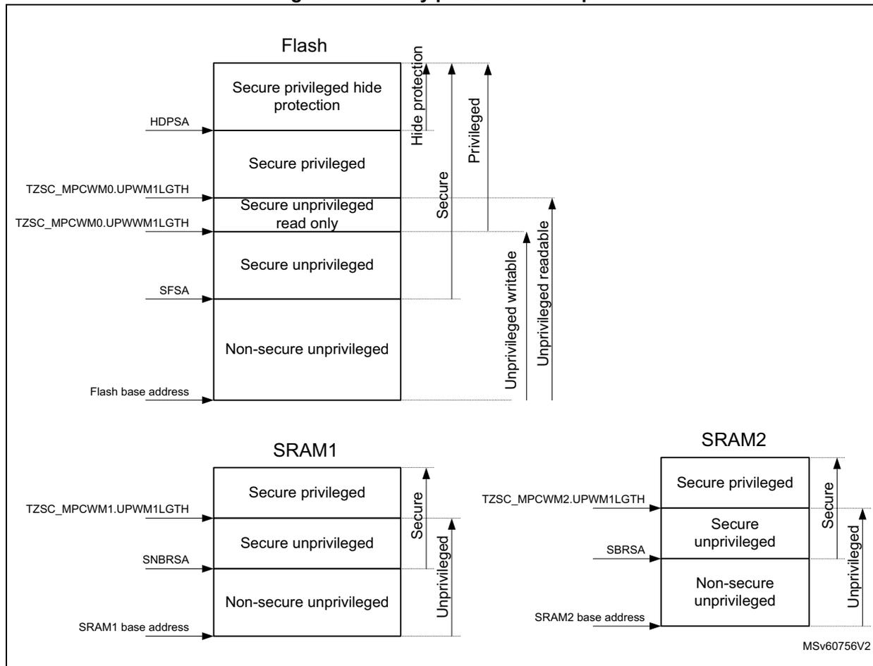
The diagram shows three memory regions: Flash, SRAM1, and SRAM2, each with different protection zones.
- Flash:
- Base address: Flash base address
- Top section: Secure privileged hide protection (accessed via HDPSA)
- Second section: Secure privileged (accessed via TZSC_MPCWM0.UPWM1LGTH)
- Third section: Secure unprivileged read only (accessed via TZSC_MPCWM0.UPVVM1LGTH)
- Fourth section: Secure unprivileged (accessed via SFSA)
- Bottom section: Non-secure unprivileged
- Access permissions (indicated by vertical arrows on the right):
- Hide protection: Secure privileged only.
- Secure: Secure privileged only.
- Privileged: Secure privileged, Secure unprivileged, and Non-secure unprivileged.
- Unprivileged: Secure unprivileged and Non-secure unprivileged.
- Unprivileged readable: Non-secure unprivileged only.
- SRAM1:
- Base address: SRAM1 base address
- Top section: Secure privileged (accessed via TZSC_MPCWM1.UPWM1LGTH)
- Second section: Secure unprivileged (accessed via SNBRSA)
- Bottom section: Non-secure unprivileged
- Access permissions (indicated by vertical arrows on the right):
- Secure: Secure privileged and Secure unprivileged.
- Unprivileged: All three sections (Secure privileged, Secure unprivileged, and Non-secure unprivileged).
- SRAM2:
- Base address: SRAM2 base address
- Top section: Secure privileged (accessed via TZSC_MPCWM2.UPWM1LGTH)
- Second section: Secure unprivileged (accessed via SBRSA)
- Bottom section: Non-secure unprivileged
- Access permissions (indicated by vertical arrows on the right):
- Secure: Secure privileged and Secure unprivileged.
- Unprivileged: All three sections (Secure privileged, Secure unprivileged, and Non-secure unprivileged).
MSV60756V2
This example show only a secure and privileged protected memory map. The security and unprivileged parameters can freely be programmed in any order as detailed below:
- • When HDPSA > SFSA > unprivileged watermark > unprivileged write watermark, the areas appear in the following order:
- – Secure privileged hide protection area at the top
- – Secure privileged area
- – Non-secure privileged area
- – Non-secure unprivileged read only area
- – Non-secure unprivileged area starting from the memory base address.
- • unprivileged write watermark >= unprivileged watermark, the areas appear in the following order:
- – privileged area at the top
- – Unprivileged area starting from the memory base address (no unprivileged read only area in this case)
Memory access protection overview
The secure area of the memories have exclusively read, write, execute access only from the secure CPU2 and secure DMA channels. CPU1 and non-secure DMA channels have no execute, read, nor write access to these areas.
The non-secure area of the memories grants full read, write, execute access to CPU1 and all DMA channels. CPU2 has only read and write access to the non-secure areas. CPU2 is prevented from executing from non-secure areas.
Access rules from the different bus masters and secure, non-secure, privileged and unprivileged access types to the different memory areas is given in the table below.
Table 3. Memory security and privilege access
| SoC level memory area | CPU2 hide protection privileged | CPU2 privileged | CPU2 unprivileged | CPU1 privileged | CPU1 unprivileged | DMA ch sub-lv secure priv | DMA ch sub-lv secure | DMA ch sub-lv non-secure | DMA ch sub-lv Non-secure | |
|---|---|---|---|---|---|---|---|---|---|---|
| Flash memory | Hide protection secure privileged | no access (1) | no access (2) | (rd, wr) (1) | no access (2) | |||||
| Secure privileged | ex, rd, wr | no access (2) | no access (2) | |||||||
| Secure privileged Unprivileged execution | ex, rd, wr | ex, rd (3) | rd | no access (2) | ||||||
| Secure unprivileged | ex, rd, wr | rd, wr | rd, wr | |||||||
| Non-secure privileged | rd, wr | rd, wr | no access (2)(4) | ex, rd, wr | no access (2)(4) | rd, wr | ||||
| Non-secure unprivileged | rd, wr | ex, rd, wr | rd, wr | rd, wr | ||||||
Table 3. Memory security and privilege access (continued)
| SoC level memory area | CPU2 hide protection privileged | CPU2 privileged | CPU2 unprivileged | CPU1 privileged | CPU1 unprivileged | DMA ch sub-lv secure priv | DMA ch sub-lv secure | DMA ch sub-lv non-secure | DMA ch sub-lv Non-secure | |
|---|---|---|---|---|---|---|---|---|---|---|
| SRAM2 | Secure privileged | ex
(5)
, rd, wr | ex
(5)
, rd, wr | no access (2) | no access (6) | no access (6) | rd, wr | no access (2)(6) | no access (2)(6) | no access (2)(6) |
| Secure unprivileged | ex
(5)
, rd, wr | rd, wr | ||||||||
| Non-secure privileged | rd, wr | rd, wr | no access (2)(4) | ex
(5)
, rd, wr | ex
(5)
, rd, wr | no access (2)(4) | rd, wr | rd, wr | ||
| Non-secure unprivileged | rd, wr | rd, wr | ||||||||
| SRAM1 | Secure privileged | ex
(5)
, rd, wr | ex
(5)
, rd, wr | no access (2) | no access (6) | no access (6) | rd, wr | no access (2) | no access (2) | no access (2) |
| Secure unprivileged | ex
(5)
, rd, wr | rd, wr | ||||||||
| Non-secure privileged | rd, wr | rd, wr | no access (2)(4) | ex
(5)
, rd, wr | ex
(5)
, rd, wr | no access (2)(4) | rd, wr | rd, wr | ||
| Non-secure unprivileged | rd, wr | rd, wr | ||||||||
- 1. Access to the hide protection secure privileged area is disabled by flash memory hide protection secure privileged HDPADIS bit.
- 2. Read access returns a zero value, write access is ignored and, in both cases, an illegal access event is generated.
- 3. The secure privileged and unprivileged, read and execute protected pages cannot be written by a secure unprivileged access. However it can be erased by a secure unprivileged page erase.
- 4. Privileged area start address < secure area start address.
- 5. Execution from SRAM1 and SRAM2 can be disabled by the execute never feature available from the MPU in the respective CPU.
- 6. Read access returns a zero value, write access is ignored and, in both cases, an illegal access event is generated. When RDP level is 1 and CPU1 boots from SRAM1, SRAM2 is locked and no illegal access event is generated.
2.6 Memory organization
2.6.1 Introduction
Program memory, data memory, registers and I/O ports are organized within the same linear address space.
The bytes are coded in memory in Little Endian format. The lowest numbered byte in a word is considered the word's least significant byte and the highest numbered byte the most significant.
2.6.2 Memory map and register boundary addresses
Figure 3. Memory map
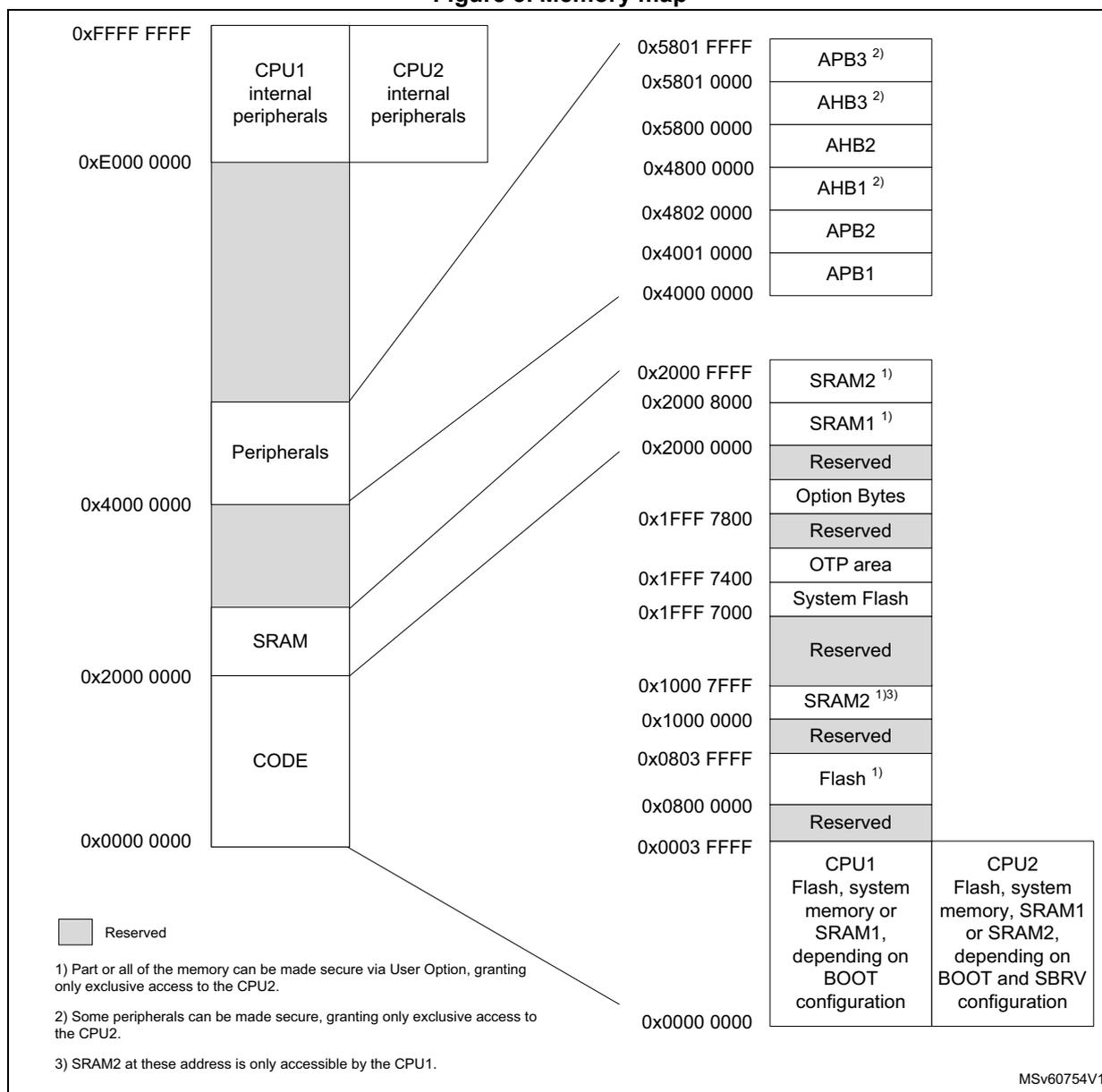
The memory map illustrates the distribution of memory between CPU1 and CPU2 internal peripherals, various system components, and user-defined CODE and SRAM regions. The diagram is divided into two main columns of addresses. The left column shows the physical memory layout from 0x0000 0000 to 0xFFFF FFFF, with regions for CODE, SRAM, Peripherals, CPU1 internal peripherals, and CPU2 internal peripherals. The right column shows the system component memory map from 0x0000 0000 to 0x5801 FFFF, including Reserved areas, Flash, SRAM2, System Flash, OTP area, Option Bytes, APB1, APB2, AHB1, AHB2, AHB3, and APB3. Lines connect the CODE and SRAM regions to their respective system addresses.
| Address Range | Component / Region |
|---|---|
| 0x0000 0000 – 0x0003 FFFF | CPU1 Flash, system memory or SRAM1, depending on BOOT configuration / CPU2 Flash, system memory, SRAM1 or SRAM2, depending on BOOT and SBRV configuration |
| 0x0003 FFFF – 0x0004 0000 | Reserved |
| 0x0004 0000 – 0x0800 0000 | Flash 1) |
| 0x0800 0000 – 0x0803 FFFF | Reserved |
| 0x0803 FFFF – 0x1000 0000 | SRAM2 1)3) |
| 0x1000 0000 – 0x1000 7FFF | Reserved |
| 0x1000 7FFF – 0x1FFF 7000 | System Flash |
| 0x1FFF 7000 – 0x1FFF 7400 | OTP area |
| 0x1FFF 7400 – 0x1FFF 7800 | Reserved |
| 0x1FFF 7800 – 0x2000 0000 | Option Bytes |
| 0x2000 0000 – 0x2000 8000 | SRAM1 1) |
| 0x2000 8000 – 0x2000 FFFF | SRAM2 1) |
| 0x2000 FFFF – 0x4000 0000 | Reserved |
| 0x4000 0000 – 0x4001 0000 | APB1 |
| 0x4001 0000 – 0x4800 0000 | APB2 |
| 0x4800 0000 – 0x4802 0000 | AHB1 2) |
| 0x4802 0000 – 0x5800 0000 | AHB2 |
| 0x5800 0000 – 0x5801 0000 | AHB3 2) |
| 0x5801 0000 – 0x5801 FFFF | APB3 2) |
Legend:
- ■ Reserved
Notes:
- Part or all of the memory can be made secure via User Option, granting only exclusive access to the CPU2.
- Some peripherals can be made secure, granting only exclusive access to the CPU2.
- SRAM2 at these address is only accessible by the CPU1.
MSv60754V1
Any memory area not allocated to on-chip memories and peripherals is considered “Reserved”.
The table below details the boundary addresses of peripherals available in the device.
Table 4. Memory map and peripheral register boundary addresses
| Bus | Boundary address | Size (bytes) | Peripheral | Peripheral register map |
|---|---|---|---|---|
| APB3 | 0x5801 0400 - 0x5801 FFFF | - | Reserved | - |
| 0x5801 0000 - 0x5801 03FF | 1 K | SUBGHZSPI | Section 37.9.10: SPI/I2S register map | |
| AHB3 | 0x5800 40C0 - 0x5800 FFFF | - | Reserved | - |
| 0x5800 4800 - 0x5800 4BFF | 1 K | GTZC_TZIC | Section 3.6.4: GTZC TZIC register map | |
| 0x5800 4400 - 0x5800 47FF | 1 K | GTZC_TZSC | Section 3.5.8: GTZC TZSC register map | |
| 0x5800 4000 - 0x5800 43FF | 1 K | FLASH | Section 4.10.21: FLASH register map | |
| 0x5800 3400 - 0x5800 3FFF | 8 K | PKA continue | Section 24.7.5: PKA register map | |
| 0x5800 2400 - 0x5800 33FF | PKA RAM | |||
| 0x5800 2000 - 0x5800 23FF | PKA | |||
| 0x5800 1C00 - 0x5800 1FFF | - | Reserved | - | |
| 0x5800 1800 - 0x5800 1BFF | 1 K | AES | Section 23.7.18: AES register map | |
| 0x5800 1400 - 0x5800 17FF | 1 K | HSEM | Section 8.4.9: HSEM register map | |
| 0x5800 1000 - 0x5800 13FF | 1 K | True RNG | Section 22.7.5: RNG register map | |
| 0x5800 0C00 - 0x5800 0FFF | 1 K | IPCC | Section 9.4.9: IPCC register map | |
| 0x5800 0800 - 0x5800 0BFF | 1 K | EXTI | Section 16.6.13: EXTI register map | |
| 0x5800 0400 - 0x5800 07FF | 1 K | PWR | Section 6.6.23: PWR register map | |
| 0x5800 0000 - 0x5800 03FF | 1 K | RCC | Section 7.4.47: RCC register map | |
| AHB2 | 0x4800 2000 - 0x57FF FFFF | - | Reserved | - |
| 0x4800 1C00 - 0x4800 1FFF | 8 K | GPIO | Section 10.4.36: GPIOH register map | |
| 0x4800 0C00 - 0x4800 1BFF | Reserved | |||
| 0x4800 0800 - 0x4800 0BFF | Section 10.4.35: GPIOC register map | |||
| 0x4800 0400 - 0x4800 07FF | Section 10.4.34: GPIOB register map | |||
| 0x4800 0000 - 0x4800 03FF | Section 10.4.33: GPIOA register map |
Table 4. Memory map and peripheral register boundary addresses (continued)
| Bus | Boundary address | Size (bytes) | Peripheral | Peripheral register map |
|---|---|---|---|---|
| AHB1 | 0x4260 0000 - 0x47FF FFFF | - | Reserved | - |
| 0x4240 0000 - 0x425F FFFF | 2048 K | AHB1 bit banding (CPU1 only) | - | |
| 0x4220 0000 - 0x423F FFFF | 2048 K | APB2 bit banding (CPU1 only) | - | |
| 0x4200 0000 - 0x421F FFFF | 2048 K | APB1 bit banding (CPU1 only) | - | |
| 0x4002 3400 - 0x41FF FFFF | - | Reserved | - | |
| 0x4002 3000 - 0x4002 33FF | 1 K | CRC | Section 17.4.6: CRC register map | |
| 0x4002 0C00 - 0x4002 2FFF | - | Reserved | - | |
| 0x4002 0800 - 0x4002 0BFF | 1 K | DMAMUX1 | Section 14.6.7: DMAMUX register map | |
| 0x4002 0400 - 0x4002 07FF | 1 K | DMA2 | Section 13.6.7: DMA register map | |
| 0x4002 0000 - 0x4002 03FF | 1 K | DMA1 | Section 13.6.7: DMA register map | |
| APB2 | 0x4001 4C00 - 0x4001 FFFF | - | Reserved | - |
| 0x4001 4800 - 0x4001 4BFF | 1 K | TIM17 | Section 27.4.23: TIM16/TIM17 register map | |
| 0x4001 4400 - 0x4001 47FF | 1 K | TIM16 | Section 27.4.23: TIM16/TIM17 register map | |
| 0x4001 3C00 - 0x4001 43FF | - | Reserved | - | |
| 0x4001 3800 - 0x4001 3BFF | 1 K | USART1 | Section 35.8.15: USART register map | |
| 0x4001 3400 - 0x4001 37FF | - | Reserved | - | |
| 0x4001 3000 - 0x4001 33FF | 1 K | SPI1 | Section 37.9.10: SPI/I2S register map | |
| 0x4001 2C00 - 0x4001 2FFF | 1 K | TIM1 | Section 25.4.30: TIM1 register map | |
| 0x4001 2800 - 0x4001 2BFF | - | Reserved | - | |
| 0x4001 2400 - 0x4001 27FF | 1 K | ADC | Section 18.13: ADC register map | |
| 0x4001 0400 - 0x4001 23FF | - | Reserved | - | |
| 0x4001 0200 - 0x4001 03FF | 1 K | COMP | Section 21.6.3: COMP register map | |
| 0x4001 0100 - 0x4001 01FF | SYSCFG continue | Section 11.2.16: SYSCFG register map | ||
| 0x4001 0030 - 0x4001 00FF | VREFBUF | Section 20.3.3: VREFBUF register map | ||
| 0x4001 0000 - 0x4001 002F | SYSCFG | Section 11.2.16: SYSCFG register map |
Table 4. Memory map and peripheral register boundary addresses (continued)
| Bus | Boundary address | Size (bytes) | Peripheral | Peripheral register map |
|---|---|---|---|---|
| APB1 | 0x4000 B400 - 0x4000 FFFF | - | Reserved | - |
| 0x4000 B000 - 0x4000 B3FF | 1 K | TAMP | Section 33.6.11: TAMP register map | |
| 0x4000 9C00 - 0x4000 AFFF | - | Reserved | - | |
| 0x4000 9800 - 0x4000 9BFF | 1 K | LPTIM3 | Section 28.7.13: LPTIM register map | |
| 0x4000 9400 - 0x4000 97FF | 1 K | LPTIM2 | Section 28.7.13: LPTIM register map | |
| 0x4000 8400 - 0x4000 93FF | - | Reserved | - | |
| 0x4000 8000 - 0x4000 83FF | 1 K | LPUART1 | Section 36.7.13: LPUART register map | |
| 0x4000 7C00 - 0x4000 7FFF | 1 K | LPTIM1 | Section 28.7.13: LPTIM register map | |
| 0x4000 7800 - 0x4000 7BFF | - | Reserved | - | |
| 0x4000 7400 - 0x4000 77FF | 1K | DAC | Section 19.7.13: DAC register map | |
| 0x4000 6000 - 0x4000 73FF | - | Reserved | - | |
| 0x4000 5C00 - 0x4000 5FFF | 1 K | I2C3 | Section 34.9.12: I2C register map | |
| 0x4000 5800 - 0x4000 5BFF | 1 K | I2C2 | Section 34.9.12: I2C register map | |
| 0x4000 5400 - 0x4000 57FF | 1 K | I2C1 | Section 34.9.12: I2C register map | |
| 0x4000 4800 - 0x4000 53FF | - | Reserved | - | |
| 0x4000 4400 - 0x4000 47FF | 1 K | USART2 | Section 35.8.15: USART register map | |
| 0x4000 3C00 - 0x4000 43FF | - | Reserved | - | |
| 0x4000 3800 - 0x4000 3BFF | 1 K | SPI2S2 | Section 37.9.10: SPI/I2S register map | |
| 0x4000 3400 - 0x4000 37FF | - | Reserved | - | |
| 0x4000 3000 - 0x4000 33FF | 1 K | IWDG | Section 30.4.6: IWDG register map | |
| 0x4000 2C00 - 0x4000 2FFF | 1 K | WWDG | Section 31.5.4: WWDG register map | |
| 0x4000 2800 - 0x4000 2BFF | 1 K | RTC | Section 32.6.23: RTC register map | |
| 0x4000 0400 - 0x4000 27FF | - | Reserved | - | |
| 0x4000 0000 - 0x4000 03FF | 1 K | TIM2 | Section 26.4.25: TIMx register map | |
| - | 0x2220 0000 - 0x3FFF FFFF | - | Reserved | - |
| AHB3 | 0x2210 0000 - 0x221F FFFF | 1024 K | SRAM2 bit banding (CPU1 only) | - |
| 0x2200 0000 - 0x220F FFFF | 1024 K | SRAM1 bit banding (CPU1 only) | - | |
| - | 0x2001 0000 - 0x21FF FFFF | - | Reserved | - |
| AHB3 | 0x2000 8000 - 0x2000 FFFF | 32 K | SRAM2 | - |
| 0x2000 0000 - 0x2000 7FFF | 32 K | SRAM1 | - | |
| - | 0x1FFF 8080 - 0x1FFF FFFF | - | Reserved | - |
| Bus | Boundary address | Size (bytes) | Peripheral | Peripheral register map |
|---|---|---|---|---|
| AHB3 | 0x1FFF 7800 - 0x1FFF 7FFF | 2 K | Flash user options | Section 4.10.21: FLASH register map |
| 0x1FFF 7400 - 0x1FFF 77FF | 1 K | Flash Engi | - | |
| 0x1FFF 7000 - 0x1FFF 73FF | 1 K | Flash OTP | - | |
| 0x1FFF 0000 - 0x1FFF 6FFF | 28 K | Flash RSS and bootloader | - | |
| - | 0x1000 8000 - 0x1FFE FFFF | - | Reserved | - |
| AHB3 | 0x1000 0000 - 0x1000 7FFF | 32 K | SRAM2 (CPU1 only) | - |
| - | 0x0804 0000 - 0x0FFF FFFF | - | Reserved | - |
| AHB3 | 0x0800 0000 - 0x0803 FFFF | 256 K | User flash (1) | - |
| - | 0x0004 0000 - 0x07FF FFFF | - | Reserved | - |
| BOOT (2) | 0x0000 0000 - 0x0003 FFFF | 256 K | CPU1n boot area | - |
1. This address corresponds to the maximum flash memory. For products with smaller flash memory size (128 and 64 Kbytes), the end address is lower.
2. Bus depends on the selected CPU1n boot area.
2.6.3 CPU1 bit banding
The CPU1 map includes two bit-band regions. These regions map each word in an alias region of memory to a bit in a bit-band region of memory. Writing to a word in the alias region has the same effect as a read-modify-write operation on the targeted bit in the bit-band region.
The AHB1, APB1, APB2 peripheral registers and the SRAM1 and SRAM2 are mapped to a bit-band region, so that single bit-band write and read operations are allowed. The operations are only available for CPU1 accesses and not from other bus masters (such as DMA).
The peripheral bit-band alias is located from address 0x4200 0000 to 0x425F FFFF.
The SRAM bit-band alias is located from address 0x2200 0000 to 0x221F FFFF.
A mapping formula shows how to reference each word in the alias region to a corresponding bit in the bit-band region.
The mapping formula is the following:
where:
- •
bit_word_addris the address of the word in the alias memory region that maps to the targeted bit. - •
bit_band_baseis the starting address of the alias region. - •
byte_offsetis the number of the byte in the bit_band region that contains the targeted bit. - •
bit_numberis the bit position (0-7) of the targeted bit.
Example
The following example shows how to map bit [2] of the byte located at SRAM1 address 0x2000 0300 to the alias region. The formula is then:
Writing to address 0x2200 6008 has the same effect as a read-modify-write operation on bit [2] of the byte at SRAM1 address 0x2000 0300.
Reading address 0x2200 6008 returns the value 0x01 or 0x00 of bit [2] of the byte at SRAM1 address 0x2000 0300.
For more information on bit-band, refer to the Cortex-M4 programming manual.