25. Device electronic signature
This section applies to all STM32L010xx devices, unless otherwise specified.
The electronic signature is stored in the System memory area in the Flash memory module, and can be read using the JTAG/SWD or the CPU. It contains factory-programmed identification data that allow the user firmware or other external devices to automatically match its interface to the characteristics of the STM32L010xx microcontroller.
25.1 Memory size register
25.1.1 Flash size register
Base address: 0x1FF8 007C
Read only = 0xXXXX where X is factory-programmed

| 15 | 14 | 13 | 12 | 11 | 10 | 9 | 8 | 7 | 6 | 5 | 4 | 3 | 2 | 1 | 0 |
| F_SIZE | |||||||||||||||
| r | r | r | r | r | r | r | r | r | r | r | r | r | r | r | r |
Bits 15:0 F_SIZE : Flash memory size
The value stored in this field indicates the Flash memory size of the device expressed in Kbytes.
Example: 0x0040 = 64 Kbytes.
25.2 Unique device ID registers (96 bits)
The unique device identifier is ideally suited:
- • for use as serial numbers
- • for use as security keys in order to increase the security of code in Flash memory while using and combining this unique ID with software cryptographic primitives and protocols before programming the internal Flash memory
- • to activate secure boot processes, etc.
The 96-bit unique device identifier provides a reference number which is unique for any device and in any context. These bits can never be altered by the user.
The 96-bit unique device identifier can also be read in single bytes/half-words/words in different ways and then be concatenated using a custom algorithm.
Base address: 0x1FF8 0050
Address offset: 0x00
Read only = 0xXXXX XXXX where X is factory-programmed
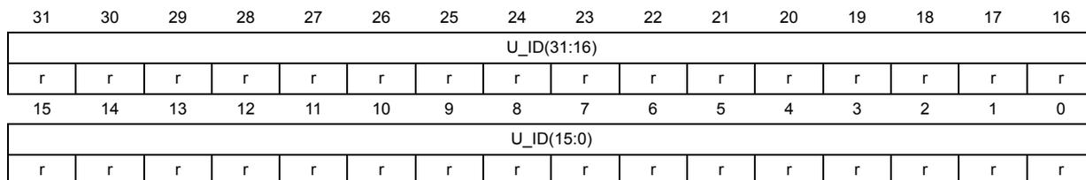
| 31 | 30 | 29 | 28 | 27 | 26 | 25 | 24 | 23 | 22 | 21 | 20 | 19 | 18 | 17 | 16 |
| U_ID(31:16) | |||||||||||||||
| r | r | r | r | r | r | r | r | r | r | r | r | r | r | r | r |
| 15 | 14 | 13 | 12 | 11 | 10 | 9 | 8 | 7 | 6 | 5 | 4 | 3 | 2 | 1 | 0 |
| U_ID(15:0) | |||||||||||||||
| r | r | r | r | r | r | r | r | r | r | r | r | r | r | r | r |
Bits 31:0 U_ID(31:24): WAF_NUM[7:0]
Wafer number (8-bit unsigned number)
U_ID(23:0): LOT_NUM[55:32]
Lot number (ASCII code)
Address offset: 0x04
Read only = 0xXXXX XXXX where X is factory-programmed
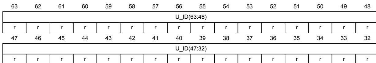
| 63 | 62 | 61 | 60 | 59 | 58 | 57 | 56 | 55 | 54 | 53 | 52 | 51 | 50 | 49 | 48 |
| U_ID(63:48) | |||||||||||||||
| r | r | r | r | r | r | r | r | r | r | r | r | r | r | r | r |
| 47 | 46 | 45 | 44 | 43 | 42 | 41 | 40 | 39 | 38 | 37 | 36 | 35 | 34 | 33 | 32 |
| U_ID(47:32) | |||||||||||||||
| r | r | r | r | r | r | r | r | r | r | r | r | r | r | r | r |
Bits 63:32 U_ID(63:32): LOT_NUM[31:0]
Lot number (ASCII code)
Address offset: 0x14
Read only = 0xXXXX XXXX where X is factory-programmed
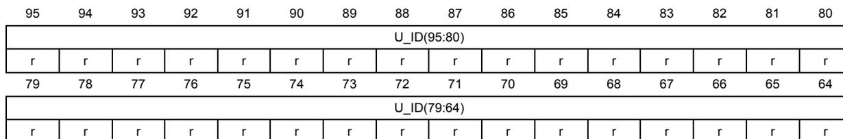
| 95 | 94 | 93 | 92 | 91 | 90 | 89 | 88 | 87 | 86 | 85 | 84 | 83 | 82 | 81 | 80 |
| U_ID(95:80) | |||||||||||||||
| r | r | r | r | r | r | r | r | r | r | r | r | r | r | r | r |
| 79 | 78 | 77 | 76 | 75 | 74 | 73 | 72 | 71 | 70 | 69 | 68 | 67 | 66 | 65 | 64 |
| U_ID(79:64) | |||||||||||||||
| r | r | r | r | r | r | r | r | r | r | r | r | r | r | r | r |
Bits 95:64 U_ID(95:64): 95:64 unique ID bits
Appendix A Code examples
A.1 Introduction
This appendix shows the code examples of the sequence described in this Reference Manual.
These code examples are extracted from the STM32L0xx Snippet firmware package STM32SnippetsL0 available on www.st.com .
These code examples used the peripheral bit and register description from the CMSIS header file (stm32l0xx.h).
Code lines starting with // should be uncommented if the given register has been modified before.
A.2 NVM/RCC Operation code example
A.2.1 Increasing the CPU frequency preparation sequence code
/* (1) Set one wait state in Latency bit of FLASH_ACR */
/* (2) Check the latency is set */
/* (3) Switch the clock on HSI16/4 and disable PLL */
/* (4) Set PLLMUL to 16 to get 32MHz on CPU clock */
/* (5) Enable and switch on PLL */
FLASH->ACR |= FLASH_ACR_LATENCY; /* (1) */
while ((FLASH->ACR & FLASH_ACR_LATENCY) == 0); /* (2) */
SwitchFromPLLtoHSI(); /* (3) */
RCC->CFGR = (RCC->CFGR & (~(uint32_t)RCC_CFGR_PLLMUL))
           | RCC_CFGR_PLLMUL16; /* (4) */
SwitchOnPLL(); /* (5) */
A.2.2 Decreasing the CPU frequency preparation sequence code
/* (1) Switch the clock on HSI16/4 and disable PLL */
/* (2) Set PLLMUL to 4 to get 8MHz on CPU clock */
/* (3) Enable and switch on PLL */
/* (4) Set one wait state in Latency bit of FLASH_ACR */
/* (5) Check the latency is set */
SwitchFromPLLtoHSI(); /* (1) */
RCC->CFGR = (RCC->CFGR & (~(uint32_t)RCC_CFGR_PLLMUL))
           | RCC_CFGR_PLLMUL4; /* (2) */
SwitchOnPLL(); /* (3) */
FLASH->ACR |= ~FLASH_ACR_LATENCY; /* (4) */
while ((FLASH->ACR & FLASH_ACR_LATENCY) != 0); /* (5) */
A.2.3 Switch from PLL to HSI16 sequence code
uint32_t tickstart;
/* (1) Switch the clock on HSI16/4 */
/* (2) Wait for clock switched on HSI16/4 */
/* (3) Disable the PLL by resetting PLLON */
/* (4) Wait until PLLRDY is cleared */
RCC->CFGR = (RCC->CFGR & (~RCC_CFGR_SW)) | RCC_CFGR_SW_HSI; /* (1) */
tickstart = Tick;
while ((RCC->CFGR & RCC_CFGR_SWS) != RCC_CFGR_SWS_HSI) /* (2) */
{
    if ((Tick - tickstart) > CLOCKSWITCH_TIMEOUT_VALUE)
    {
        /* Manage error */
        return;
    }
}
RCC->CR &= ~RCC_CR_PLLON; /* (3) */
tickstart = Tick;
while ((RCC->CR & RCC_CR_PLLRDY) != 0) /* (4) */
{
    if ((Tick - tickstart) > PLL_TIMEOUT_VALUE)
    {
        /* Manage error */
    }
}
Note: Tick is a global variable incremented in the SysTick ISR each millisecond.
A.2.4 Switch to PLL sequence code
uint32_t tickstart;
/* (1) Switch on the PLL */
/* (2) Wait for PLL ready */
/* (3) Switch the clock to the PLL */
/* (4) Wait until the clock is switched to the PLL */
RCC->CR |= RCC_CR_PLLON; /* (1) */
tickstart = Tick;
while ((RCC->CR & RCC_CR_PLLRDY) == 0) /* (2) */
{
    if ((Tick - tickstart) > PLL_TIMEOUT_VALUE)
    {
        error = ERROR_PLL_TIMEOUT; /* Report an error */
        return;
    }
}
RCC->CFGR = (RCC->CFGR & (~RCC_CFGR_SW)) | RCC_CFGR_SW_PLL; /* (3) */
tickstart = Tick;
while ((RCC->CFGR & RCC_CFGR_SWS) != RCC_CFGR_SWS_PLL) /* (4) */
{
    if ((Tick - tickstart) > CLOCKSWITCH_TIMEOUT_VALUE)
    {
        error = ERROR_CLKSWITCH_TIMEOUT; /* Report an error */
        return;
    }
}
Note: Tick is a global variable incremented in the SysTick ISR each millisecond.
A.3 NVM Operation code example
A.3.1 Unlocking the data EEPROM and FLASH_PECR register code example
/* (1) Wait till no operation is on going */
/* (2) Check if the PELOCK is unlocked */
/* (3) Perform unlock sequence */
while ((FLASH->SR & FLASH_SR_BSY) != 0) /* (1) */
{
    /* For robust implementation, add here time-out management */
}
if ((FLASH->PECR & FLASH_PECR_PELOCK) != 0) /* (2) */
{
    FLASH->PEKEYR = FLASH_PEKEY1; /* (3) */
    FLASH->PEKEYR = FLASH_PEKEY2;
}
A.3.2 Locking data EEPROM and FLASH_PECR register code example
/* (1) Wait till no operation is on going */
/* (2) Locks the NVM by setting PELOCK in PECR */
while ((FLASH->SR & FLASH_SR_BSY) != 0) /* (1) */
{
    /* For robust implementation, add here time-out management */
}
FLASH->PECR |= FLASH_PECR_PELOCK; /* (2) */
A.3.3 Unlocking the NVM program memory code example
/* (1) Wait till no operation is on going */
/* (2) Check that the PELOCK is unlocked */
/* (3) Check if the PRGLOCK is unlocked */
/* (4) Perform unlock sequence */
while ((FLASH->SR & FLASH_SR_BSY) != 0) /* (1) */
{
    /* For robust implementation, add here time-out management */
}
if ((FLASH->PECR & FLASH_PECR_PELOCK) != 0) /* (2) */
{
    FLASH->PEKEYR = FLASH_PEKEY1; /* (3) */
    FLASH->PEKEYR = FLASH_PEKEY2;
}
if ((FLASH->PECR & FLASH_PECR_PRGLOCK) != 0) /* (3) */
{
    FLASH->PEKEYR = FLASH_PEKEY1; /* (3) */
    FLASH->PEKEYR = FLASH_PEKEY2;
}
FLASH->PECR |= FLASH_PECR_PRGLOCK; /* (4) */
{
    /* For robust implementation, add here time-out management */
}
if ((FLASH->PECR & FLASH_PECR_PELOCK) == 0) /* (2) */
{
    if ((FLASH->PECR & FLASH_PECR_PRGLOCK) != 0) /* (3) */
    {
        FLASH->PRGKEYR = FLASH_PRGKEY1; /* (4) */
        FLASH->PRGKEYR = FLASH_PRGKEY2;
    }
}
A.3.4 Unlocking the option bytes area code example
/* (1) Wait till no operation is on going */
/* (2) Check that the PELOCK is unlocked */
/* (3) Check if the OPTLOCK is unlocked */
/* (4) Perform unlock sequence */
while ((FLASH->SR & FLASH_SR_BSY) != 0) /* (1) */
{
    /* For robust implementation, add here time-out management */
}
if ((FLASH->PECR & FLASH_PECR_PELOCK) == 0) /* (2) */
{
    if ((FLASH->PECR & FLASH_PECR_OPTLOCK) != 0) /* (2) */
    {
        FLASH->OPTKEYR = FLASH_OPTKEY1; /* (3) */
        FLASH->OPTKEYR = FLASH_OPTKEY2;
    }
}
A.3.5 Write to data EEPROM code example
*(uint8_t *) (DATA_E2_ADDR+i) = DATA_BYTE;
*(uint16_t *) (DATA_E2_ADDR+j) = DATA_16B_WORD;
*(uint32_t *) (DATA_E2_ADDR) = DATA_32B_WORD;
DATA_E2_ADDR is an aligned address in the data EEPROM area.
i can be any integer.
j must be an even integer.
A.3.6 Erase to data EEPROM code example
/* (1) Set the ERASE and DATA bits in the FLASH_PECR register
      to enable page erasing */
/* (2) Write a 32-bit word value at the desired address
      to start the erase sequence */
/* (3) Enter in wait for interrupt. The EOP check is done in the Flash ISR
 */
/* (6) Reset the ERASE and DATA bits in the FLASH_PECR register
 to disable the page erase */
FLASH->PECRI |= FLASH_PECRI_ERASE | FLASH_PECRI_DATA; /* (1) */
*( __IO uint32_t *)addr = (uint32_t)0; /* (2) */
__WFI(); /* (3) */
FLASH->PECRI &= ~(FLASH_PECRI_ERASE | FLASH_PECRI_DATA); /* (4) */
A.3.7 Program Option byte code example
/**
 * This function programs a 16-bit option byte and its complement word.
 * Param None
 * Retval None
 */
__INLINE __RAM_FUNC void OptionByteProg(uint8_t index, uint16_t data)
{
    /* (1) Write a 32-bit word value at the option byte address,
 the 16-bit data is extended with its complemented value */
    /* (3) Wait until the BSY bit is reset in the FLASH_SR register */
    /* (4) Check the EOP flag in the FLASH_SR register */
    /* (5) Clear EOP flag by software by writing EOP at 1 */
    *( __IO uint32_t *)(OB_BASE + index) = (uint32_t)((~data << 16) | data);
    /* (1) */
    while ((FLASH->SR & FLASH_SR_BSY) != 0) /* (2) */
    {
        /* For robust implementation, add here time-out management */
    }
    if ((FLASH->SR & FLASH_SR_EOP) != 0) /* (3) */
    {
        FLASH->SR = FLASH_SR_EOP; /* (4) */
    }
    else
    {
        /* Manage the error cases */
    }
}
Note: This function must be loaded in RAM.
A.3.8 Erase Option byte code example
/**
 * This function erases a 16-bit option byte and its complement
 * word.
 * Param None
 */
    * Retval None
*/
__INLINE __RAM_FUNC void OptionByteErase(uint8_t index)
{
    /* (1) Set the ERASE bit in the FLASH_PECR register
       to enable option byte erasing */
    /* (2) Write a 32-bit word value at the option byte address to be erased
       to start the erase sequence */
    /* (3) Wait until the BSY bit is reset in the FLASH_SR register */
    /* (4) Check the EOP flag in the FLASH_SR register */
    /* (5) Clear EOP flag by software by writing EOP at 1 */
    /* (6) Reset the ERASE and PROG bits in the FLASH_PECR register
       to disable the page erase */
    FLASH->PECRI |= FLASH_PECRI_ERASE; /* (1) */
    *(volatile uint32_t *)(OB_BASE + index) = 0; /* (2) */
    while ((FLASH->SR & FLASH_SR_BSY) != 0) /* (3) */
    {
        /* For robust implementation, add here time-out management */
    }
    if ((FLASH->SR & FLASH_SR_EOP) != 0) /* (4) */
    {
        FLASH->SR |= FLASH_SR_EOP; /* (5) */
    }
    else
    {
        /* Manage the error cases */
    }
    FLASH->PECRI &= ~(FLASH_PECRI_ERASE); /* (6) */
}
Note: This function must be loaded in RAM.
A.3.9 Program a single word to Flash program memory code example
    /* (1) Perform the data write (32-bit word) at the desired address */
    /* (2) Wait until the BSY bit is reset in the FLASH_SR register */
    /* (3) Check the EOP flag in the FLASH_SR register */
    /* (4) clear it by software by writing it at 1 */
    *(volatile uint32_t*)(flash_addr) = data; /* (1) */
    while ((FLASH->SR & FLASH_SR_BSY) != 0) /* (2) */
    {
        /* For robust implementation, add here time-out management */
    }
    if ((FLASH->SR & FLASH_SR_EOP) != 0) /* (3) */
    {
        FLASH->SR = FLASH_SR_EOP; /* (4) */
    }
}
    }
else
{
    /* Manage the error cases */
}
A.3.10 Program half-page to Flash program memory code example
/**
 * This function programs a half page. It is executed from the RAM.
 * The Programming bit (PROG) and half-page programming bit (FPRG)
 * is set at the beginning and reset at the end of the function,
 * in case of successive programming, these two operations
 * could be performed outside the function.
 * This function waits the end of programming, clears the appropriate
 * bit in the Status register and eventually reports an error.
 * Param flash_addr is the first address of the half-page to be programmed
 * data is the 32-bit word array to program
 * Retval None
 */
__RAM_FUNC void FlashHalfPageProg(uint32_t flash_addr, uint32_t *data)
{
    uint8_t i;
    /* (1) Set the PROG and FPRG bits in the FLASH_PECR register
       to enable a half page programming */
    /* (2) Perform the data write (half-word) at the desired address */
    /* (3) Wait until the BSY bit is reset in the FLASH_SR register */
    /* (4) Check the EOP flag in the FLASH_SR register */
    /* (5) clear it by software by writing it at 1 */
    /* (6) Reset the PROG and FPRG bits to disable programming */
    FLASH->PECR |= FLASH_PECR_PROG | FLASH_PECR_FPRG; /* (1) */
    for (i = 0; i < ((FLASH_PAGE_SIZE/2) / 4); i++)
    {
        *(__IO uint32_t*)(flash_addr) = *data++; /* (2) */
    }
    while ((FLASH->SR & FLASH_SR_BSY) != 0) /* (3) */
    {
        /* For robust implementation, add here time-out management */
    }
    if ((FLASH->SR & FLASH_SR_EOP) != 0) /* (4) */
    {
        FLASH->SR = FLASH_SR_EOP; /* (5) */
    }
    else
    {
        /* Manage the error cases */
    }
    FLASH->PECR &= ~(FLASH_PECR_PROG | FLASH_PECR_FPRG); /* (6) */
}
Note: This function must be loaded in RAM.
A.3.11 Erase a page in Flash program memory code example
/**
 * This function erases a page of flash.
 * The Page Erase bit (PER) is set at the beginning and reset
 * at the end of the function, in case of successive erase,
 * these two operations could be performed outside the function.
 * Param page_addr is an address inside the page to erase
 * Retval None
 */
__INLINE void FlashErase(uint32_t page_addr)
{
    /* (1) Set the ERASE and PROG bits in the FLASH_PECR register
        to enable page erasing */
    /* (2) Write a 32-bit word value in an address of the selected page
        to start the erase sequence */
    /* (3) Wait until the BSY bit is reset in the FLASH_SR register */
    /* (4) Check the EOP flag in the FLASH_SR register */
    /* (5) Clear EOP flag by software by writing EOP at 1 */
    /* (6) Reset the ERASE and PROG bits in the FLASH_PECR register
        to disable the page erase */
    FLASH->PECR |= FLASH_PECR_ERASE | FLASH_PECR_PROG; /* (1) */
    *(volatile uint32_t *)page_addr = (uint32_t)0; /* (2) */
    while ((FLASH->SR & FLASH_SR_BSY) != 0) /* (3) */
    {
        /* For robust implementation, add here time-out management */
    }
    if ((FLASH->SR & FLASH_SR_EOP) != 0) /* (4) */
    {
        FLASH->SR = FLASH_SR_EOP; /* (5) */
    }
    else
    {
        /* Manage the error cases */
    }
    FLASH->PECR &= ~(FLASH_PECR_ERASE | FLASH_PECR_PROG); /* (6) */
}
A.3.12 Mass erase code example
/**
 * This function performs a mass erase of the flash.
 * This function is loaded in RAM.
 * Param None
 * Retval while successful, the function never returns except if executed
 * from RAM
 */
__RAM_FUNC void FlashMassErase(void)
{
    /* (1) Check if the read protection is not level 2 */
    /* (2) Check if the read protection is not level 1 */
    /* (3) Erase the Option byte containing the read protection */
    /* (4) Reload the Option bytes */
    /* (5) Program read protection to level 1 by writing 0xAA
       to start the mass erase */
    /* (6) Lock the NVM by setting the PELOCK bit */
    if ((FLASH->OPTR & 0x000000FF) == 0xCC) /* (1) */
    {
        /* Report the error and abort*/
        return;
    }
    else if ((FLASH->OPTR & 0x000000FF) == 0xAA) /* (2) */
    {
        OptionByteErase(FLASH_OPTR0); /* (3) */
        FLASH->PECR |= FLASH_PECR_OBL_LAUNCH; /* (4) */
        /* The MCU will reset while executing the option bytes reloading */
    }
    OptionByteProg(FLASH_OPTR0, 0x00AA); /* (5) */
    if (*(uint32_t *)(FLASH_MAIN_ADDR) != (uint32_t)0) /* Check the erasing
    of the page by reading all the page value */
    {
        /* Report the error */
    }
    LockNVM(); /* (6) */
    while (1) /* Infinite loop */
    {
    }
}
Note: This function uses two other ones in A.3.7: Program Option byte code example and A.3.8: Erase Option byte code example .
A.4 Clock Controller
A.4.1 HSE start sequence code example
/**
 * This function enables the interrupt HSE ready,
 * and start the HSE as external clock.
 * Param None
 * Retval None
 */
__INLINE void StartHSE(void)
{
    /* Configure NVIC for RCC */
    /* (1) Enable Interrupt on RCC */
    /* (2) Set priority for RCC */
    NVIC_EnableIRQ(RCC_CRS_IRQn); /* (1) */
    NVIC_SetPriority(RCC_CRS_IRQn, 0); /* (2) */

    /* (1) Enable interrupt on HSE ready */
    /* (2) Enable the CSS
       Enable the HSE and set HSEBYP to use the external clock
       instead of an oscillator
       Enable HSE */
    /* Note : the clock is switched to HSE in the RCC_CRS_IRQHandler ISR */
    RCC->CIER |= RCC_CIER_HSERDYIE; /* (1) */
    RCC->CR |= RCC_CR_CSSHSEON | RCC_CR_HSEBYP | RCC_CR_HSEON; /* (2) */
}

/**
 * This function handles RCC interrupt request
 * and switch the system clock to HSE.
 * Param None
 * Retval None
 */
void RCC_CRS_IRQHandler(void)
{
    /* (1) Check the flag HSE ready */
    /* (2) Clear the flag HSE ready */
    /* (3) Switch the system clock to HSE */
    if ((RCC->CifR & RCC_CifR_HSERDYF) != 0) /* (1) */
    {
        RCC->CICR |= RCC_CICR_HSERDYC; /* (2) */
        RCC->CFGR = ((RCC->CFGR & (~RCC_CFGR_SW)) | RCC_CFGR_SW_HSE); /* (3) */
    }
    else
    {
    }
}
{
/* Manage error */
}
}A.4.2 PLL configuration modification code example
/* (1) Test if PLL is used as System clock */
/* (2) Select HSI as system clock */
/* (3) Wait for HSI switched */
/* (4) Disable the PLL */
/* (5) Wait until PLLRDY is cleared */
/* (6) Set latency to 1 wait state */
/* (7) Set the PLL multiplier to 24 and divider by 3 */
/* (8) Enable the PLL */
/* (9) Wait until PLLRDY is set */
/* (10) Select PLL as system clock */
/* (11) Wait until the PLL is switched on */
if ((RCC->CFGR & RCC_CFGR_SWS) == RCC_CFGR_SWS_PLL) /* (1) */
{
    RCC->CFGR = (RCC->CFGR & (uint32_t) (~RCC_CFGR_SW))
                | RCC_CFGR_SW_HSI; /* (2) */
    while ((RCC->CFGR & RCC_CFGR_SWS) != RCC_CFGR_SWS_HSI) /* (3) */
    {
        /* For robust implementation, add here time-out management */
    }
}
RCC->CR &= (uint32_t) (~RCC_CR_PLLON); /* (4) */
while ((RCC->CR & RCC_CR_PLLRDY) != 0) /* (5) */
{
    /* For robust implementation, add here time-out management */
}
FLASH->ACR |= FLASH_ACR_LATENCY; /* (6) */
RCC->CFGR = RCC->CFGR & (~ (RCC_CFGR_PLLMUL | RCC_CFGR_PLLDIV ))
           | (RCC_CFGR_PLLMUL24 | RCC_CFGR_PLLDIV2); /* (7) */
RCC->CR |= RCC_CR_PLLON; /* (8) */
while ((RCC->CR & RCC_CR_PLLRDY) == 0) /* (9) */
{
    /* For robust implementation, add here time-out management */
}
RCC->CFGR |= (uint32_t) (RCC_CFGR_SW_PLL); /* (10) */
while ((RCC->CFGR & RCC_CFGR_SWS) != RCC_CFGR_SWS_PLL) /* (11) */
{
    /* For robust implementation, add here time-out management */
}
A.4.3 MCO selection code example
/* (1) Clear the MCO selection bits */
/* (2) Select system clock/4 to be output on the MCO without prescaler */
RCC->CFGR &= (uint32_t) RCC_CFGR_MCOSEL; /* (1) */
RCC->CFGR |= RCC_CFGR_MCO_SYSCLK | RCC_CFGR_MCO_PRE_4; /* (2) */
A.5 GPIOs
A.5.1 Locking mechanism code example
/* (1) Write LCKK bit to 1 and set the pin bits to lock */
/* (2) Write LCKK bit to 0 and set the pin bits to lock */
/* (3) Write LCKK bit to 1 and set the pin bits to lock */
/* (4) Read the Lock register */
/* (5) Check the Lock register (optional) */
GPIOA->LCKR = GPIO_LCKR_LCKK + lock; /* (1) */
GPIOA->LCKR = lock; /* (2) */
GPIOA->LCKR = GPIO_LCKR_LCKK + lock; /* (3) */
GPIOA->LCKR; /* (4) */
if ((GPIOA->LCKR & GPIO_LCKR_LCKK) == 0) /* (5) */
{
    /* Manage error */
}
A.5.2 Alternate function selection sequence code example
/* (1) Enable the peripheral clock of Timer 2 */
/* (2) Enable the peripheral clock of GPIOA */
/* (3) Select Alternate function mode (10) on GPIOA pin 0 */
/* (4) Select TIM2_CH1 on PA0 by enabling AF2 for pin 0 in GPIOA AFRL
   register */
RCC->APB1ENR |= RCC_APB1ENR_TIM2EN; /* (1) */
RCC->IOPENR |= RCC_IOPENR_GPIOAEN; /* (2) */
GPIOA->MODER = (GPIOA->MODER & ~(GPIO_MODER_MODE0)) \
                | (GPIO_MODER_MODE0_1); /* (3) */
GPIOA->AFR[0] |= 0x2; /* (4) */
A.5.3 Analog GPIO configuration code example
/* (1) Enable the peripheral clock of GPIOA */
/* (2) Select Input float mode (00- default) on GPIOA pin 0 */
RCC->IOPENR |= RCC_IOPENR_GPIOAEN; /* (1) */
GPIOA->MODER &= ~(GPIO_MODER_MODE0); /* (2) */
A.6 DMA
A.6.1 DMA Channel Configuration sequence code example
/* (1) Enable the peripheral clock on DMA */
/* (2) Remap DMA channel1 on ADC (reset value) */
/* (3) Enable DMA transfer on ADC */
/* (4) Configure the peripheral data register address */
/* (5) Configure the memory address */
/* (6) Configure the number of DMA transfer to be performed on channel 1 */
/* (7) Configure increment, size and interrupts */
/* (8) Enable DMA Channel 1 */
RCC->AHBENR |= RCC_AHBENR_DMA1EN; /* (1) */
//DMA1_CSELR->CSELR &= (uint32_t)(~DMA_CSELR_C1S); /* (2) */
ADC1->CFGR1 |= ADC_CFGR1_DMAEN; /* (3) */
DMA1_Channel1->CPAR = (uint32_t) (&(ADC1->DR)); /* (4) */
DMA1_Channel1->CMAR = (uint32_t)(ADC_array); /* (5) */
DMA1_Channel1->CNDTR = 3; /* (6) */
DMA1_Channel1->CCR |= DMA_CCR_MINC | DMA_CCR_MSIZE_0 | DMA_CCR_PSIZE_0 \
                       | DMA_CCR_TEIE | DMA_CCR_TCIE ; /* (7) */
DMA1_Channel1->CCR |= DMA_CCR_EN; /* (8) */

/* Configure NVIC for DMA */
/* (1) Enable Interrupt on DMA Channel 1 */
/* (2) Set priority for DMA Channel 1 */
NVIC_EnableIRQ(DMA1_Channel1_IRQn); /* (1) */
NVIC_SetPriority(DMA1_Channel1_IRQn,0); /* (2) */
A.7 Interrupts and event
A.7.1 NVIC initialization example
/* Configure NVIC for ADC */
/* (1) Enable Interrupt on ADC */
/* (2) Set priority for ADC */
NVIC_EnableIRQ(ADC1_COMP_IRQn); /* (1) */
NVIC_SetPriority(ADC1_COMP_IRQn,0); /* (2) */
A.7.2 Extended interrupt selection code example
/* (1) Enable the peripheral clock of GPIOA */
/* (2) Select input mode (00) on GPIOA pin 0 */
/* (3) Select Port A for pin 0 extended interrupt by writing 0000
   in EXTI0 (reset value) */
/* (4) Configure the corresponding mask bit in the EXTI_IMR register */
/* (5) Configure the Trigger Selection bits of the Interrupt line
   on rising edge */
/* (6) Configure the Trigger Selection bits of the Interrupt line
   on falling edge */
RCC->IOPENR |= RCC_IOPENR_GPIOAEN; /* (1) */
GPIOA->MODER = (GPIOA->MODER & ~(GPIO_MODER_MODE0)); /* (2) */
//SYSCFG->EXTICR[0] &= (uint16_t)~SYSCFG_EXTICR1_EXTI0_PA; /* (3) */
EXTI->IMR |= 0x0001; /* (4) */
EXTI->RTSR |= 0x0001; /* (5) */
//EXTI->FTSR |= 0x0001; /* (6) */

/* Configure NVIC for Extended Interrupt */
/* (7) Enable Interrupt on EXTI0_1 */
/* (8) Set priority for EXTI0_1 */
NVIC_EnableIRQ(EXTI0_1_IRQn); /* (7) */
NVIC_SetPriority(EXTI0_1_IRQn,0); /* (8) */
A.8 ADC
A.8.1 Calibration code example
/* (1) Ensure that ADEN = 0 */
/* (2) Clear ADEN */
/* (3) Set ADCAL=1 */
/* (4) Wait until EOCAL=1 */
/* (5) Clear EOCAL */
if ((ADC1->CR & ADC_CR_ADEN) != 0) /* (1) */
{
    ADC1->CR |= ADC_CR_ADDIS; /* (2) */
}
ADC1->CR |= ADC_CR_ADCAL; /* (3) */
while ((ADC1->ISR & ADC_ISR_EOCAL) == 0) /* (4) */
{
    /* For robust implementation, add here time-out management */
}
ADC1->ISR |= ADC_ISR_EOCAL; /* (5) */
A.8.2 ADC enable sequence code example
/* (1) Clear the ADRDY bit */
/* (2) Enable the ADC */
/* (3) Wait until ADC ready */
ADC1->ISR |= ADC_ISR_ADRDY; /* (1) */
ADC1->CR |= ADC_CR_ADEN; /* (2) */
if ((ADC1->CFGR1 & ADC_CFGR1_AUTOFF) == 0)
{
    while ((ADC1->ISR & ADC_ISR_ADRDY) == 0) /* (3) */
    {
        /* For robust implementation, add here time-out management */
    }
}
A.8.3 ADC disable sequence code example
/* (1) Ensure that no conversion on going */
/* (2) Stop any ongoing conversion */
/* (3) Wait until ADSTP is reset by hardware i.e. conversion is stopped */
/* (4) Disable the ADC */
/* (5) Wait until the ADC is fully disabled */
if ((ADC1->CR & ADC_CR_ADSTART) != 0) /* (1) */
{
    ADC1->CR |= ADC_CR_ADSTP; /* (2) */
}
while ((ADC1->CR & ADC_CR_ADSTP) != 0) /* (3) */
{
    /* For robust implementation, add here time-out management */
}
ADC1->CR |= ADC_CR_ADDIS; /* (4) */
while ((ADC1->CR & ADC_CR_ADEN) != 0) /* (5) */
{
    /* For robust implementation, add here time-out management */
}
A.8.4 ADC clock selection code example
/* (1) Select PCLK by writing 11 in CKMODE */
ADC1->CFGR2 |= ADC_CFGR2_CKMODE; /* (1) */
A.8.5 Single conversion sequence code example - Software trigger
/* (1) Select HSI16 by writing 00 in CKMODE (reset value) */
/* (2) Select the auto off mode */
/* (3) Select CHSEL17 for VRefInt */
/* (4) Select a sampling mode of 111 i.e. 239.5 ADC clk to be greater than
    17.1us */
/* (5) Wake-up the VREFINT (only for VRefInt) */
//ADC1->CFGR2 &= ~ADC_CFGR2_CKMODE; /* (1) */
ADC1->CFGR1 |= ADC_CFGR1_AUTOFF; /* (2) */
ADC1->CHSELR = ADC_CHSELR_CHSEL17; /* (3) */
ADC1->SMPR |= ADC_SMPR_SMP_0 | ADC_SMPR_SMP_1 | ADC_SMPR_SMP_2; /* (4) */
ADC->CCR |= ADC_CCR_VREFEN; /* (5) */
...
/* Performs the AD conversion */
ADC1->CR |= ADC_CR_ADSTART; /* start the ADC conversion */
while ((ADC1->ISR & ADC_ISR_EOC) == 0) /* wait end of conversion */
{
    /* For robust implementation, add here time-out management */
}
A.8.6 Continuous conversion sequence code example - Software trigger
/* (1) Select HSI16 by writing 00 in CKMODE (reset value) */
/* (2) Select the continuous mode and scanning direction */
/* (3) Select CHSEL4, CHSEL9 and CHSEL17 */
/* (4) Select a sampling mode of 111 i.e. 239.5 ADC clk to be greater
   than 5 us */
/* (5) Enable interrupts on EOC, ESEQ and overrun */
/* (6) Wake-up the VREFINT (only for VRefInt) */
//ADC1->CFGR2 &= ~ADC_CFGR2_CKMODE; /* (1) */
ADC1->CFGR1 |= ADC_CFGR1_WAIT | ADC_CFGR1_CONT | ADC_CFGR1_SCANDIR; /* (2) */
ADC1->CHSELR = ADC_CHSELR_CHSEL4 | ADC_CHSELR_CHSEL9 \
               | ADC_CHSELR_CHSEL17; /* (3) */
ADC1->SMPR |= ADC_SMPR_SMP_0 | ADC_SMPR_SMP_1 | ADC_SMPR_SMP_2; /* (4) */
ADC1->IER = ADC_IER_EOCIE | ADC_IER_ESEQIE | ADC_IER_OVRIE; /* (5) */
ADC->CCR |= ADC_CCR_VREFEN; /* (6) */

/* Configure NVIC for ADC */
/* (1) Enable Interrupt on ADC */
/* (2) Set priority for ADC */
NVIC_EnableIRQ(ADC1_COMP_IRQn); /* (1) */
NVIC_SetPriority(ADC1_COMP_IRQn, 0); /* (2) */
A.8.7 Single conversion sequence code example - Hardware trigger
/* (1) Select HSI16 by writing 00 in CKMODE (reset value) */
/* (2) Select the external trigger on falling edge and external trigger on
   TIM22_TRGO by selecting TRG4 (EXTSEL = 100) */
/* (3) Select CHSEL17 for VRefInt */
/* (4) Select a sampling mode of 111 i.e. 239.5 ADC clk to be greater
   than 5us */
/* (5) Wake-up the VREFINT (only for VRefInt) */
//ADC1->CFGR2 &= ~ADC_CFGR2_CKMODE; /* (1) */
ADC1->CFGR1 |= ADC_CFGR1_EXTEN_0 | ADC_CFGR1_EXTSEL_2 ; /* (2) */
ADC1->CHSELR = ADC_CHSELR_CHSEL17; /* (3) */
ADC1->SMPR |= ADC_SMPR_SMP_0 | ADC_SMPR_SMP_1 | ADC_SMPR_SMP_2; /* (4) */
ADC->CCR |= ADC_CCR_VREFEN; /* (5) */
Note: Then TIM22 must be configured to generate an external trigger on TRGO periodically.
A.8.8 Continuous conversion sequence code example - Hardware trigger
/* (1) Select HSI16 by writing 00 in CKMODE (reset value) */
/* (2) Select the external trigger on TIM22_TRGO (TRG4 i.e. EXTSEL = 100
   and rising edge, the continuous mode and scanning direction */
/* (3) Select CHSEL4, CHSEL9 and CHSEL17 */
/* (4) Select a sampling mode of 111 i.e. 239.5 ADC clk to be greater
   than 5us */
/* (5) Enable interrupts on EOC, EOSEQ and overrun */
/* (6) Wake-up the VREFINT (only for VRefInt) */
//ADC1->CFGR2 &= ~ADC_CFGR2_CKMODE; /* (1) */
ADC1->CFGR1 |= ADC_CFGR1_EXTEN_0 | ADC_CFGR1_EXTSEL_2 | ADC_CFGR1_CONT \
    | ADC_CFGR1_SCANDIR; /* (2) */
ADC1->CHSELR = ADC_CHSELR_CHSEL4 | ADC_CHSELR_CHSEL9 \
    | ADC_CHSELR_CHSEL17; /* (3) */
ADC1->SMPR |= ADC_SMPR_SMP_0 | ADC_SMPR_SMP_1 | ADC_SMPR_SMP_2; /* (4) */
ADC1->IER = ADC_IER_EOCIE | ADC_IER_EOSEQIE | ADC_IER_OVRIE; /* (5) */
ADC->CCR |= ADC_CCR_VREFEN; /* (6) */
/* Configure NVIC for ADC */
/* (1) Enable Interrupt on ADC */
/* (2) Set priority for ADC */
NVIC_EnableIRQ(ADC1_COMP_IRQn); /* (1) */
NVIC_SetPriority(ADC1_COMP_IRQn,0); /* (2) */
A.8.9 DMA one shot mode sequence code example
/* (1) Enable the peripheral clock on DMA */
/* (2) Enable DMA transfer on ADC - DMACFG is kept at 0 for one shot mode */
/* (3) Configure the peripheral data register address */
/* (4) Configure the memory address */
/* (5) Configure the number of DMA transfer to be performed
   on DMA channel 1 */
/* (6) Configure increment, size and interrupts */
/* (7) Enable DMA Channel 1 */
RCC->AHBENR |= RCC_AHBENR_DMA1EN; /* (1) */
ADC1->CFGR1 |= ADC_CFGR1_DMAEN; /* (2) */
DMA1_Channel1->CPAR = (uint32_t) (&(ADC1->DR)); /* (3) */
DMA1_Channel1->CMAR = (uint32_t) (ADC_array); /* (4) */
DMA1_Channel1->CNDTR = NUMBER_OF_ADC_CHANNEL; /* (5) */
DMA1_Channel1->CCR |= DMA_CCR_MINC | DMA_CCR_MSIZE_0 | DMA_CCR_PSIZE_0 \
    | DMA_CCR_TEIE | DMA_CCR_TCIE ; /* (6) */
DMA1_Channel1->CCR |= DMA_CCR_EN; /* (7) */
A.8.10 DMA circular mode sequence code example
/* (1) Enable the peripheral clock on DMA */
/* (2) Enable DMA transfer on ADC and circular mode */
/* (3) Configure the peripheral data register address */
/* (4) Configure the memory address */
/* (5) Configure the number of DMA transfer to be performed
   on DMA channel 1 */
/* (6) Configure increment, size, interrupts and circular mode */
/* (7) Enable DMA Channel 1 */
RCC->AHBENR |= RCC_AHBENR_DMA1EN; /* (1) */
ADC1->CFGR1 |= ADC_CFGR1_DMAEN | ADC_CFGR1_DMACFG; /* (2) */
DMA1_Channel1->CPAR = (uint32_t) (&(ADC1->DR)); /* (3) */
DMA1_Channel1->CMAR = (uint32_t) (ADC_array); /* (4) */
DMA1_Channel1->CNDTR = NUMBER_OF_ADC_CHANNEL; /* (5) */
DMA1_Channel1->CCR |= DMA_CCR_MINC | DMA_CCR_MSIZE_0 | DMA_CCR_PSIZE_0 \
    | DMA_CCR_TEIE | DMA_CCR_CIRC; /* (6) */
DMA1_Channel1->CCR |= DMA_CCR_EN; /* (7) */
A.8.11 Wait mode sequence code example
/* (1) Select PCLK by writing 11 in CKMODE */
/* (2) Select the continuous mode and the wait mode */
/* (3) Select CHSEL4, CHSEL9 and CHSEL17 */
/* (4) Select a sampling mode of 111 i.e. 239.5 ADC clk to be greater
   than 17.1us */
/* (5) Enable interrupts on overrun */
/* (6) Wake-up the VREFINT (only for VRefInt) */
ADC1->CFGR2 |= ADC_CFGR2_CKMODE; /* (1) */
ADC1->CFGR1 |= ADC_CFGR1_CONT | ADC_CFGR1_WAIT; /* (2) */
ADC1->CHSELR = ADC_CHSELR_CHSEL4 | ADC_CHSELR_CHSEL9 \
    | ADC_CHSELR_CHSEL17; /* (3) */
ADC1->SMPR |= ADC_SMPR_SMP_0 | ADC_SMPR_SMP_1 | ADC_SMPR_SMP_2; /* (4) */
ADC1->IER = ADC_IER_OVRIE; /* (5) */
ADC->CCR |= ADC_CCR_VREFEN; /* (6) */
A.8.12 Auto off and no wait mode sequence code example
/* (1) Select HSI16 by writing 00 in CKMODE (reset value) */
/* (2) Select the external trigger on TIM22_TRGO and falling edge,
   the continuous mode, scanning direction and auto off */
/* (3) Select CHSEL4, CHSEL9 and CHSEL17 */
/* (4) Select a sampling mode of 111 i.e. 239.5 ADC clk to be greater
   than 5us */
/* (5) Enable interrupts on EOC, EOEQ and overrun */
/* (6) Wake-up the VREFINT (only for VRefInt) */
//ADC1->CFGR2 &= ~ADC_CFGR2_CKMODE; /* (1) */
ADC1->CFGR1 |= ADC_CFGR1_EXTEN_0 | ADC_CFGR1_EXTSEL_2 \
               | ADC_CFGR1_SCANDIR | ADC_CFGR1_AUTOFF; /* (2) */
ADC1->CHSELR = ADC_CHSELR_CHSEL4 | ADC_CHSELR_CHSEL9 \
               | ADC_CHSELR_CHSEL17; /* (3) */
ADC1->SMPR |= ADC_SMPR_SMP_0 | ADC_SMPR_SMP_1 | ADC_SMPR_SMP_2; /* (4) */
ADC1->IER = ADC_IER_EOCIE | ADC_IER_EOSEQIE | ADC_IER_OVRIE; /* (5) */
ADC->CCR |= ADC_CCR_VREFEN; /* (6) */
A.8.13 Auto off and wait mode sequence code example
/* (1) Select HSI16 by writing 00 in CKMODE (reset value) */
/* (2) Select the continuous mode, the wait mode and the Auto off */
/* (3) Select CHSEL4, CHSEL9 and CHSEL17 */
/* (4) Select a sampling mode of 111 i.e. 239.5 ADC clk to be greater
   than 5us */
/* (5) Enable interrupt on overrun */
/* (6) Wake-up the VREFINT (only for VRefInt) */
//ADC1->CFGR2 &= ~ADC_CFGR2_CKMODE; /* (1) */
ADC1->CFGR1 |= ADC_CFGR1_CONT | ADC_CFGR1_WAIT | ADC_CFGR1_AUTOFF; /* (2) */
ADC1->CHSELR = ADC_CHSELR_CHSEL4 | ADC_CHSELR_CHSEL9 \
               | ADC_CHSELR_CHSEL17; /* (3) */
ADC1->SMPR |= ADC_SMPR_SMP_0 | ADC_SMPR_SMP_1 | ADC_SMPR_SMP_2; /* (4) */
ADC1->IER = ADC_IER_OVRIE; /* (5) */
ADC->CCR |= ADC_CCR_VREFEN; /* (6) */
A.8.14 Analog watchdog code example
/* Define the upper limit 15% above the factory value
   the value is adapted according to the application power supply
   versus the factory calibration power supply */
uint16_t vrefint_high = (*VREFINT_CAL_ADDR)* VDD_CALIB / VDD_APPLI * 115 /
100;

/* Define the lower limit 15% below the factory value
   the value is adapted according to the application power supply
   versus the factory calibration power supply */
uint16_t vrefint_low = (*VREFINT_CAL_ADDR) * VDD_CALIB / VDD_APPLI * 85 /
100;

/* (1) Select HSI16 by writing 00 in CKMODE (reset value) */
/* (2) Select the continuous mode
   and configure the Analog watchdog to monitor only CH17 */
/* (3) Define analog watchdog range : 16b-MSW is the high limit
   and 16b-LSW is the low limit */
/* (4) Select CHSEL4, CHSEL9 and CHSEL17 */
/* (5) Select a sampling mode of 111 i.e. 239.5 ADC clk to be greater
   than 5us */
/* (6) Enable interrupts on EOC, ESEQ and Analog Watchdog */
/* (7) Wake-up the VREFINT (only for VBAT and VRefInt) */
//ADC1->CFGR2 &= ~ADC_CFGR2_CKMODE; /* (1) */
ADC1->CFGR1 |= ADC_CFGR1_CONT \
    | (17<<26) | ADC_CFGR1_AWDEN | ADC_CFGR1_AWDSEL; /* (2) */
ADC1->TR = (vrefint_high << 16) + vrefint_low; /* (3) */
ADC1->CHSELR = ADC_CHSELR_CHSEL4 | ADC_CHSELR_CHSEL9 \
    | ADC_CHSELR_CHSEL17; /* (4) */
ADC1->SMPR |= ADC_SMPR_SMP_0 | ADC_SMPR_SMP_1 | ADC_SMPR_SMP_2; /* (5) */
ADC1->IER = ADC_IER_EOCIE | ADC_IER_ESEQIE | ADC_IER_AWDIE; /* (6) */
ADC->CCR |= ADC_CCR_VREFEN; /* (7) */
A.8.15 Oversampling code example
/* (1) Select HSI16 by writing 00 in CKMODE (reset value)
   Enable oversampling with ratio 16 and shifted by 1,
   without trigger */
ADC1->CFGR2 = (ADC1->CFGR2 & (~ADC_CFGR2_CKMODE)) \
    | (ADC_CFGR2_OVSE | ADC_CFGR2_OVSR_1 | ADC_CFGR2_OVSR_0 \
    | ADC_CFGR2_OVSS_0); /* (1) */
A.9 Timers
A.9.1 Upcounter on TI2 rising edge code example
/* (1) Configure channel 1 to detect rising edges on the TI1 input
   by writing CC1S = '01', and configure the input filter
   duration by writing the IC1F[3:0] bits in the TIMx_CCMR1
   register (if no filter is needed, keep IC2F=0000).*/
/* (2) Select rising edge polarity by writing CC1P=0 in the TIMx_CCER
   register
   Not necessary as it keeps the reset value. */
/* (3) Configure the timer in external clock mode 1 by writing SMS=111
   Select TI1 as the trigger input source by writing TS=101
   in the TIMx_SMCR register. */
/* (4) Enable the counter by writing CEN=1 in the TIMx_CR1 register. */
TIMx->CCMR1 |= TIM_CCMR1_IC1F_0 | TIM_CCMR1_IC1F_1 \
    | TIM_CCMR1_CC1S_0; /* (1) */
//TIMx->CCER &= (uint16_t)(~TIM_CCER_CC1P); /* (2) */
TIMx->SMCR |= TIM_SMCR_SMS | TIM_SMCR_TS_2 | TIM_SMCR_TS_0; /* (3) */
TIMx->CR1 |= TIM_CR1_CEN; /* (4) */
A.9.2 Up counter on each 2 ETR rising edges code example
/* (1) As no filter is needed in this example, write ETF[3:0]=0000
   in the TIMx_SMCR register. Keep the reset value. */
Set the prescaler by writing ETPS[1:0]=01 in the TIMx_SMCR
register.
Select rising edge detection on the ETR pin by writing ETP=0
in the TIMx_SMCR register. Keep the reset value.
Enable external clock mode 2 by writing ECE=1 in the TIMx_SMCR
register. */
/* (2) Enable the counter by writing CEN=1 in the TIMx_CR1 register. */
TIMx->SMCR |= TIM_SMCR_ETPS_0 | TIM_SMCR_ECE; /* (1) */
TIMx->CR1 |= TIM_CR1_CEN; /* (2) */
A.9.3 Input capture configuration code example
/* (1) Select the active input TI1 (CC1S = 01),
    program the input filter for 8 clock cycles (IC1F = 0011),
    select the rising edge on CC1 (CC1P = 0, reset value)
    and prescaler at each valid transition (IC1PS = 00, reset value) */
/* (2) Enable capture by setting CC1E */
/* (3) Enable interrupt on Capture/Compare */
/* (4) Enable counter */
TIMx->CCMR1 |= TIM_CCMR1_CC1S_0 \
               | TIM_CCMR1_IC1F_0 | TIM_CCMR1_IC1F_1; /* (1) */
TIMx->CCER |= TIM_CCER_CC1E; /* (2) */
TIMx->DIER |= TIM_DIER_CC1IE; /* (3) */
TIMx->CR1 |= TIM_CR1_CEN; /* (4) */
A.9.4 Input capture data management code example
This code must be inserted in the timer interrupt subroutine.
if ((TIMx->SR & TIM_SR_CC1IF) != 0)
{
    if ((TIMx->SR & TIM_SR_CC1OF) != 0) /* Check the overflow */
    {
        /* Overflow error management */
        gap = 0; /* Reinitialize the laps computing */
        TIMx->SR = ~(TIM_SR_CC1OF | TIM_SR_CC1IF); /* Clear the flags */
        return;
    }
    if (gap == 0) /* Test if it is the first rising edge */
    {
        counter0 = TIMx->CCR1; /* Read the capture counter which clears the
CC1ICF */
        gap = 1; /* Indicate that the first rising edge has yet been detected */
    }
    else
    {
        counter1 = TIMx->CCR1; /* Read the capture counter which clears the
CC1ICF */
    }
}
    if (counter1 > counter0) /* Check capture counter overflow */
    {
        Counter = counter1 - counter0;
    }
    else
    {
        Counter = counter1 + 0xFFFF - counter0 + 1;
    }
    counter0 = counter1;
}
}
else
{
    /* Manage error */
}
Note: This code manages only single counter overflows. To manage several counter overflows, the update interrupt must be enabled (UIE = 1) and properly managed.
A.9.5 PWM input configuration code example
/* (1) Select the active input TI1 for TIMx_CCR1 (CC1S = 01),
   select the active input TI1 for TIMx_CCR2 (CC2S = 10) */
/* (2) Select TI1FP1 as valid trigger input (TS = 101)
   configure the slave mode in reset mode (SMS = 100) */
/* (3) Enable capture by setting CC1E and CC2E
   select the rising edge on CC1 and CC1N (CC1P = 0 and CC1NP = 0,
   reset value),
   select the falling edge on CC2 (CC2P = 1). */
/* (4) Enable interrupt on Capture/Compare 1 */
/* (5) Enable counter */
TIMx->CCMR1 |= TIM_CCMR1_CC1S_0 | TIM_CCMR1_CC2S_1; /* (1) */
TIMx->SMCR |= TIM_SMCR_TS_2 | TIM_SMCR_TS_0 \
             | TIM_SMCR_SMS_2; /* (2) */
TIMx->CCER |= TIM_CCER_CC1E | TIM_CCER_CC2E | TIM_CCER_CC2P; /* (3) */
TIMx->DIER |= TIM_DIER_CC1IE; /* (4) */
TIMx->CR1 |= TIM_CR1_CEN; /* (5) */
A.9.6 PWM input with DMA configuration code example
/* (1) Enable the peripheral clock on DMA */
/* (2) Remap DMA channel5 and 7 on TIM2_CH1 and TIM2_CH2
   by writing 1000 in DMA_CSELR_C5S and DMA_CSELR_C7S */
/* (3) Configure the peripheral data register address for DMA channel x */
/* (4) Configure the memory address for DMA channel x */
/* (5) Configure the number of DMA transfer to be performed
   on DMA channel x */
/* (6) Configure no increment (reset value), size (16-bits), interrupts,
   transfer from peripheral to memory and circular mode
   for DMA channel x */
/* (7) Enable DMA Channel x */
RCC->AHBENR |= RCC_AHBENR_DMA1EN; /* (1) */
DMA1_CSELR->CSELR |= 8 << (4 * (5-1)) | 8 << (4 * (7-1)); /* (2) */
DMA1_Channel5->CPAR = (uint32_t) (&(TIMx->CCR1)); /* (3) */
DMA1_Channel5->CMAR = (uint32_t) (&Period); /* (4) */
DMA1_Channel5->CNDTR = 1; /* (5) */
DMA1_Channel5->CCR |= DMA_CCR_MSIZE_0 | DMA_CCR_PSIZE_0 \
    | DMA_CCR_TEIE | DMA_CCR_CIRC; /* (6) */
DMA1_Channel5->CCR |= DMA_CCR_EN; /* (7) */
/* repeat (3) to (6) for channel 6 */
DMA1_Channel7->CPAR = (uint32_t) (&(TIMx->CCR2)); /* (2) */
DMA1_Channel7->CMAR = (uint32_t) (&DutyCycle); /* (3) */
DMA1_Channel7->CNDTR = 1; /* (4) */
DMA1_Channel7->CCR |= DMA_CCR_MSIZE_0 | DMA_CCR_PSIZE_0 \
    | DMA_CCR_TEIE | DMA_CCR_CIRC; /* (5) */
DMA1_Channel7->CCR |= DMA_CCR_EN; /* (6) */

/* Configure NVIC for DMA */
/* (1) Enable Interrupt on DMA Channels x */
/* (2) Set priority for DMA Channels x */
NVIC_EnableIRQ(DMA1_Channel4_5_6_7_IRQn); /* (1) */
NVIC_SetPriority(DMA1_Channel4_5_6_7_IRQn, 3); /* (2) */
A.9.7 Output compare configuration code example
/* (1) Set prescaler to 3, so APBCLK/4 i.e 4MHz */
/* (2) Set ARR = 4000 - 1 */
/* (3) Set CCRx = ARR, as timer clock is 4MHz, an event occurs each 1 ms */
/* (4) Select toggle mode on OC1 (OC1M = 011),
   disable preload register on OC1 (OC1PE = 0, reset value) */
/* (5) Select active high polarity on OC1 (CC1P = 0, reset value),
   enable the output on OC1 (CC1E = 1 */
/* (6) Enable output (MOE = 1 */
/* (7) Enable counter */
TIMx->PSC |= 3; /* (1) */
TIMx->ARR = 4000 - 1; /* (2) */
TIMx->CCR1 = 4000 - 1; /* (3) */
TIMx->CCMR1 |= TIM_CCMR1_OC1M_0 | TIM_CCMR1_OC1M_1; /* (4) */
TIMx->CCER |= TIM_CCER_CC1E; /* (5) */
TIMx->CR1 |= TIM_CR1_CEN; /* (6) */
A.9.8 Edge-aligned PWM configuration example
/* (1) Set prescaler to 15, so APBCLK/16 i.e 1MHz */
/* (2) Set ARR = 8, as timer clock is 1MHz the period is 9 us */
/* (3) Set CCRx = 4, , the signal will be high during 4 us */
/* (4) Select PWM mode 1 on OC1 (OC1M = 110),
       enable preload register on OC1 (OC1PE = 1) */
/* (5) Select active high polarity on OC1 (CC1P = 0, reset value),
       enable the output on OC1 (CC1E = 1) */
/* (6) Enable output (MOE = 1)- optional*/
/* (7) Enable counter (CEN = 1)
       select edge aligned mode (CMS = 00, reset value)
       select direction as upcounter (DIR = 0, reset value) */
/* (8) Force update generation (UG = 1) */
TIMx->PSC = 15; /* (1) */
TIMx->ARR = 8; /* (2) */
TIMx->CCR1 = 4; /* (3) */
TIMx->CCMR1 |= TIM_CCMR1_OC1M_2 | TIM_CCMR1_OC1M_1
               | TIM_CCMR1_OC1PE; /* (4) */
TIMx->CCER |= TIM_CCER_CC1E; /* (5) */
TIMx->CR1 |= TIM_CR1_CEN; /* (6) */
TIMx->EGR |= TIM_EGR_UG; /* (7) */
A.9.9 Center-aligned PWM configuration example
/* (1) Set prescaler to 15, so APBCLK/16 i.e 1MHz */
/* (2) Set ARR = 8, as timer clock is 1MHz and center-aligned counting,
       the period is 16 us */
/* (3) Set CCRx = 7, the signal will be high during 14 us */
/* (4) Select PWM mode 1 on OC1 (OC1M = 110),
       enable preload register on OC1 (OC1PE = 1, reset value) */
/* (5) Select active high polarity on OC1 (CC1P = 0, reset value),
       enable the output on OC1 (CC1E = 1 */
/* (6) Enable output (MOE = 1 */
/* (7) Enable counter (CEN = 1)
       select center-aligned mode 1 (CMS = 01) */
/* (8) Force update generation (UG = 1) */
TIMx->PSC = 15; /* (1) */
TIMx->ARR = 8; /* (2) */
TIMx->CCR1 = 7; /* (3) */
TIMx->CCMR1 |= TIM_CCMR1_OC1M_2 | TIM_CCMR1_OC1M_1
               | TIM_CCMR1_OC1PE; /* (4) */
TIMx->CCER |= TIM_CCER_CC1E; /* (5) */
TIMx->CR1 |= TIM_CR1_CMS_0 | TIM_CR1_CEN; /* (6) */
TIMx->EGR |= TIM_EGR_UG; /* (7) */
A.9.10 ETR configuration to clear OCxREF code example
/* (1) Set prescaler to 15, so APBCLK/16 i.e 1MHz */
/* (2) Set ARR = 8, as timer clock is 1MHz the period is 9 us */
/* (3) Set CCRx = 4, , the signal will be high during 4 us */
/* (4) Select PWM mode 1 on OC1 (OC1M = 110),
       enable preload register on OC1 (OC1PE = 1)
       enable clearing on OC1 for ETR clearing (OC1CE = 1)*/
/* (5) Select active high polarity on OC1 (CC1P = 0, reset value),
       enable the output on OC1 (CC1E = 1)*/
/* (6) Select ETR as OCREF clear source (reserved bit = 1)
       select External Trigger Prescaler off (ETPS = 00, reset value)
       disable external clock mode 2 (ECE = 0, reset value)
       select active at high level (ETP = 0, reset value) */
/* (7) Enable counter (CEN = 1)
       select edge aligned mode (CMS = 00, reset value)
       select direction as upcounter (DIR = 0, reset value) */
/* (8) Force update generation (UG = 1) */

TIMx->PSC = 15; /* (1) */
TIMx->ARR = 8; /* (2) */
TIMx->CCR1 = 4; /* (3) */
TIMx->CCMR1 |= TIM_CCMR1_OC1M_2 | TIM_CCMR1_OC1M_1 | TIM_CCMR1_OC1PE \
               | TIM_CCMR1_OC1CE; /* (4) */
TIMx->CCER |= TIM_CCER_CC1E; /* (5) */
TIMx->SMCR |= (1<<3); /* (6) */
TIMx->CR1 |= TIM_CR1_CEN; /* (7) */
TIMx->EGR |= TIM_EGR_UG; /* (8) */
A.9.11 Encoder interface code example
/* (1) Configure TI1FP1 on TI1 (CC1S = 01)
       configure TI1FP2 on TI2 (CC2S = 01) */
/* (2) Configure TI1FP1 and TI1FP2 non inverted (CC1P = CC2P = 0, reset
       value) */
/* (3) Configure both inputs are active on both rising and falling edges
       (SMS = 011) */
/* (4) Enable the counter by writing CEN=1 in the TIMx_CR1 register. */
TIMx->CCMR1 |= TIM_CCMR1_CC1S_0 | TIM_CCMR1_CC2S_0; /* (1) */
//TIMx->CCER &= (uint16_t)(~(TIM_CCER_CC21 | TIM_CCER_CC2P)); /* (2) */
TIMx->SMCR |= TIM_SMCR_SMS_0 | TIM_SMCR_SMS_1; /* (3) */
TIMx->CR1 |= TIM_CR1_CEN; /* (4) */
A.9.12 Reset mode code example
/* (1) Configure channel 1 to detect rising edges on the TI1 input
   by writing CC1S = '01',
   and configure the input filter duration by writing the IC1F[3:0]
   bits
   in the TIMx_CCMR1 register (if no filter is needed, keep
   IC1F=0000).*/
/* (2) Select rising edge polarity by writing CC1P=0 in the TIMx_CCER
   register
   Not necessary as it keeps the reset value. */
/* (3) Configure the timer in reset mode by writing SMS=100
   Select TI1 as the trigger input source by writing TS=101
   in the TIMx_SMCR register.*/
/* (4) Set prescaler to 16000-1 in order to get an increment each 1ms */
/* (5) Enable the counter by writing CEN=1 in the TIMx_CR1 register. */
TIMx->CCMR1 |= TIM_CCMR1_CC1S_0; /* (1) */
//TIMx->CCER &= (uint16_t)(~TIM_CCER_CC1P); /* (2) */
TIMx->SMCR |= TIM_SMCR_SMS_2 | TIM_SMCR_TS_2 | TIM_SMCR_TS_0; /* (3) */
TIMx->PSC = 15999; /* (4) */
TIMx->CR1 |= TIM_CR1_CEN; /* (5) */
A.9.13 Gated mode code example
/* (1) Configure channel 1 to detect low level on the TI1 input
   by writing CC1S = '01',
   and configure the input filter duration by writing the IC1F[3:0]
   bits
   in the TIMx_CCMR1 register (if no filter is needed, keep
   IC1F=0000).*/
/* (2) Select polarity by writing CC1P=1 in the TIMx_CCER register */
/* (3) Configure the timer in gated mode by writing SMS=101
   Select TI1 as the trigger input source by writing TS=101
   in the TIMx_SMCR register.*/
/* (4) Set prescaler to 4000-1 in order to get an increment each 250us */
/* (5) Enable the counter by writing CEN=1 in the TIMx_CR1 register. */
TIMx->CCMR1 |= TIM_CCMR1_CC1S_0; /* (1) */
TIMx->CCER |= TIM_CCER_CC1P; /* (2) */
TIMx->SMCR |= TIM_SMCR_SMS_2 | TIM_SMCR_SMS_0 \
             | TIM_SMCR_TS_2 | TIM_SMCR_TS_0; /* (3) */
TIMx->PSC = 3999; /* (4) */
TIMx->CR1 |= TIM_CR1_CEN; /* (5) */
A.9.14 Trigger mode code example
/* (1) Configure channel 2 to detect rising edge on the TI2 input
   by writing CC2S = '01',
   and configure the input filter duration by writing the IC1F[3:0]
   bits
   in the TIMx_CCMR1 register (if no filter is needed, keep
   IC1F=0000).*/
/* (2) Select polarity by writing CC2P=0 (reset value) in the TIMx_CCER
   register */
/* (3) Configure the timer in trigger mode by writing SMS=110
   Select TI2 as the trigger input source by writing TS=110
   in the TIMx_SMCR register.*/
/* (4) Set prescaler to 4000-1 in order to get an increment each 250us */
TIMx->CCMR1 |= TIM_CCMR1_CC2S_0; /* (1) */
//TIMx->CCER &= ~TIM_CCER_CC2P; /* (2) */
TIMx->SMCR |= TIM_SMCR_SMS_2 | TIM_SMCR_SMS_1 \
             | TIM_SMCR_TS_2 | TIM_SMCR_TS_1; /* (3) */
TIMx->PSC = 3999; /* (4) */
A.9.15 External clock mode 2 + trigger mode code example
/* (1) Configure no input filter (ETF=0000, reset value)
   configure prescaler disabled (ETPS = 0, reset value)
   select detection on rising edge on ETR (ETP = 0, reset value)
   enable external clock mode 2 (ECE = 1 */
/* (2) Configure no input filter (IC1F=0000, reset value)
   select input capture source on TI1 (CC1S = 01) */
/* (3) Select polarity by writing CC1P=0 (reset value) in the TIMx_CCER
   register */
/* (4) Configure the timer in trigger mode by writing SMS=110
   Select TI1 as the trigger input source by writing TS=101
   in the TIMx_SMCR register.*/
TIMx->SMCR |= TIM_SMCR_ECE; /* (1) */
TIMx->CCMR1 |= TIM_CCMR1_CC1S_0; /* (2) */
//TIMx->CCER &= ~TIM_CCER_CC1P; /* (3) */
TIMx->SMCR |= TIM_SMCR_SMS_2 | TIM_SMCR_SMS_1 \
             | TIM_SMCR_TS_2 | TIM_SMCR_TS_0; /* (4) */
A.9.16 One-Pulse mode code example
/* The OPM waveform is defined by writing the compare registers */
/* (1) Set prescaler to 15, so APBCLK/16 i.e 1MHz */
/* (2) Set ARR = 7, as timer clock is 1MHz the period is 8 us */
/* (3) Set CCRx = 5, the burst will be delayed for 5 us (must be > 0 */
/* (4) Select PWM mode 2 on OC1 (OC1M = 111),
        enable preload register on OC1 (OC1PE = 1, reset value)
        enable fast enable (no delay) if PULSE_WITHOUT_DELAY is set*/
        /* (5) Select active high polarity on OC1 (CC1P = 0, reset value),
           enable the output on OC1 (CC1E = 1 */
        /* (6) Enable output (MOE = 1) */
        /* (7) Write '1 in the OPM bit in the TIMx_CR1 register to stop the
           counter
           at the next update event (OPM = 1)
           enable auto-reload register(ARPE = 1) */
        TIMx->PSC = 15; /* (1) */
        TIMx->ARR = 7; /* (2) */
        TIMx->CCR1 = 5; /* (3) */
        TIMx->CCMR1 |= TIM_CCMR1_OC1M_2 | TIM_CCMR1_OC1M_1 | TIM_CCMR1_OC1M_0
                       | TIM_CCMR1_OC1PE
        #if PULSE_WITHOUT_DELAY > 0
                        | TIM_CCMR1_OC1FE
        #endif
        ; /* (4) */
        TIMx->CCER |= TIM_CCER_CC1E; /* (5) */
        TIMx->CR1 |= TIM_CR1_OPM | TIM_CR1_ARPE; /* (6) */
A.9.17 Timer prescaling another timer code example
        /* (1) Select Update Event as Trigger output (TRGO) by writing MMS = 010
           in TIMx_CR2. */
        /* (2) Configure TIMy in slave mode using ITR1 as internal trigger
           by writing TS = 000 in TIMy_SMCR (reset value)
           Configure TIMy in external clock mode 1, by writing SMS=111 in the
           TIMy_SMCR register. */
        /* (3) Set TIMx prescaler to 15999 in order to get an increment each 1ms */
        /* (4) Set TIMx Autoreload to 999 in order to get an overflow (so an UEV)
           each second */
        /* (5) Set TIMx Autoreload to 24*3600-1 in order to get an overflow
           each 24-hour */
        /* (6) Enable the counter by writing CEN=1 in the TIMx_CR1 register. */
        /* (7) Enable the counter by writing CEN=1 in the TIMy_CR1 register. */
        TIMx->CR2 |= TIM_CR2_MMS_1; /* (1) */
        TIMy->SMCR |= TIM_SMCR_SMS_2 | TIM_SMCR_SMS_1 | TIM_SMCR_SMS_0; /* (2) */
        TIMx->PSC = 15999; /* (3) */
        TIMx->ARR = 999; /* (4) */
        TIMy->ARR = (24 * 3600) - 1; /* (5) */
        TIMx->CR1 |= TIM_CR1_CEN; /* (6) */
        TIMy->CR1 |= TIM_CR1_CEN; /* (7) */
A.9.18 Timer enabling another timer code example
/* (1) Configure Timer x master mode to send its Output Compare 1
Reference (OC1REF)
signal as trigger output (MMS=100 in the TIMx_CR2 register). */
/* (2) Configure the Timer x OC1REF waveform (TIMx_CCMR1 register)
Channel 1 is in PWM mode 1 when the counter is less than the
capture/compare
register (write OC1M = 110) */
/* (3) Configure TIMy in slave mode using ITR1 as internal trigger
by writing TS = 000 in TIMy_SMCR (reset value)
Configure TIMy in gated mode, by writing SMS=101 in the
TIMy_SMCR register. */
/* (4) Set TIMx prescaler to 2 */
/* (5) Set TIMy prescaler to 2 */
/* (6) Set TIMx Autoreload to 999 in order to get an overflow (so an UEV)
each 100ms */
/* (7) Set capture compare register to a value between 0 and 999 */
TIMx->CR2 |= TIM_CR2_MMS_2; /* (1) */
TIMx->CCMR1 |= TIM_CCMR1_OC1M_2 | TIM_CCMR1_OC1M_1; /* (2) */
TIMy->SMCR |= TIM_SMCR_SMS_2 | TIM_SMCR_SMS_0; /* (3) */
TIMx->PSC = 2; /* (4) */
TIMy->PSC = 2; /* (5) */
TIMx->ARR = 999; /* (6) */
TIMx->CCR1 = 700; /* (7) */

/* Configure the slave timer to generate toggling on each count */
/* (1) Configure the Timer 2 in PWM mode 1 (write OC1M = 110) */
/* (2) Set TIMx Autoreload to 1 */
/* (3) Set capture compare register to 1 */
TIMy->CCMR1 |= TIM_CCMR1_OC1M_2 | TIM_CCMR1_OC1M_1; /* (1) */
TIMy->ARR = 1; /* (2) */
TIMy->CCR1 = 1; /* (3) */
/* Enable the output of TIMx OC1 */
/* (1) Select active high polarity on OC1 (CC1P = 0, reset value),
enable the output on OC1 (CC1E = 1 */
/* (2) Enable output (MOE = 1 */
TIMx->CCER |= TIM_CCER_CC1E;

/* Enable the output of TIMy OC1 */
/* (1) Select active high polarity on OC1 (CC1P = 0, reset value),
enable the output on OC1 (CC1E = 1 */
/* (2) Enable output (MOE = 1 */
TIMy->CCER |= TIM_CCER_CC1E;
/* (1) Enable the slave counter first by writing CEN=1 in the TIMy_CR1
register. */
/* (2) Enable the master counter by writing CEN=1 in the TIMx_CR1
register. */
TIMy->CR1 |= TIM_CR1_CEN; /* (1) */
TIMx->CR1 |= TIM_CR1_CEN; /* (2) */
A.9.19 Master and slave synchronization code example
/* (1) Configure Timer x in master mode to send its enable signal
as trigger output (MMS=001 in the TIMx_CR2 register). */
/* (2) Configure the Timer x Channel 1 waveform (TIMx_CCMR1 register)
is in PWM mode 1 (write OC1M = 110) */
/* (3) Configure TIMy in slave mode using ITR1 as internal trigger
by writing TS = 000 in TIMy_SMCR (reset value)
Configure TIMy in gated mode, by writing SMS=101 in the
TIMy_SMCR register. */
/* (4) Set TIMx prescaler to 2 */
/* (5) Set TIMy prescaler to 2 */
/* (6) Set TIMx Autoreload to 99 in order to get an overflow (so an UEV)
each 10ms */
/* (7) Set capture compare register to a value between 0 and 99 */
TIMx->CR2 |= TIM_CR2_MMS_0; /* (1) */
TIMx->CCMR1 |= TIM_CCMR1_OC1M_2 | TIM_CCMR1_OC1M_1; /* (2) */
TIMy->SMCR |= TIM_SMCR_SMS_2 | TIM_SMCR_SMS_0; /* (3) */
TIMx->PSC = 2; /* (4) */
TIMy->PSC = 2; /* (5) */
TIMx->ARR = 99; /* (6) */
TIMx->CCR1 = 25; /* (7) */

/* Configure the slave timer Channel 1 as PWM as Timer to show
synchronicity */
/* (1) Configure the Timer y in PWM mode 1 (write OC1M = 110) */
/* (2) Set TIMx Autoreload to 99 */
/* (3) Set capture compare register to 25 */
TIMy->CCMR1 |= TIM_CCMR1_OC1M_2 | TIM_CCMR1_OC1M_1; /* (1) */
TIMy->ARR = 99; /* (2) */
TIMy->CCR1 = 25; /* (3) */

/* Enable the output of TIMx OC1 */
/* (1) Select active high polarity on OC1 (CC1P = 0, reset value),
enable the output on OC1 (CC1E = 1 */
/* (2) Enable output (MOE = 1 */
TIMx->CCER |= TIM_CCER_CC1E;
/* Enable the output of TIMy OC1 */
/* (1) Select active high polarity on OC1 (CC1P = 0, reset value),
        enable the output on OC1 (CC1E = 1 */
        /* (2) Enable output (MOE = 1 */
        TIMy->CCER |= TIM_CCER_CC1E;
        /* (1) Reset Timer x by writing '1 in UG bit (TIMx_EGR register) */
        /* (2) Reset Timer y by writing '1 in UG bit (TIMy_EGR register) */
        TIMx->EGR |= TIM_EGR_UG;
        TIMy->EGR |= TIM_EGR_UG;
        /* (1) Enable the slave counter first by writing CEN=1
           in the TIMy_CR1 register.
           TIMy will start synchronously with the master timer*/
        /* (2) Start the master counter by writing CEN=1 in the TIMx_CR1
           register. */
        TIMy->CR1 |= TIM_CR1_CEN; /* (1) */
        TIMx->CR1 |= TIM_CR1_CEN; /* (2) */
A.9.20 Two timers synchronized by an external trigger code example
        /* (1) Configure TIMx master mode to send its enable signal
           as trigger output (MMS=001 in the TIMx_CR2 register). */
        /* (2) Configure TIMx in slave mode to get the input trigger from TI1
           by writing TS = 100 in TIMx_SMCR
           Configure TIMx in trigger mode, by writing SMS=110 in the
           TIMx_SMCR register.
           Configure TIMx in Master/Slave mode by writing MSM = 1
           in TIMx_SMCR */
        /* (3) Configure TIMy in slave mode to get the input trigger from Timer1
           by writing TS = 000 in TIMy_SMCR (reset value)
           Configure TIMy in trigger mode, by writing SMS=110 in the
           TIMy_SMCR register. */
        /* (4) Reset Timer x counter by writing '1' in UG bit (TIMx_EGR register) */
        /* (5) Reset Timer y counter by writing '1' in UG bit (TIMy_EGR register) */
        TIMx->CR2 |= TIM_CR2_MMS_0; /* (1) */
        TIMx->SMCR |= TIM_SMCR_TS_2 | TIM_SMCR_SMS_2 | TIM_SMCR_SMS_1
                     | TIM_SMCR_MSM; /* (2) */
        TIMy->SMCR |= TIM_SMCR_SMS_2 | TIM_SMCR_SMS_1; /* (3) */
        TIMx->EGR |= TIM_EGR_UG; /* (4) */
        TIMy->EGR |= TIM_EGR_UG; /* (5) */

        /* Configure the Timer Channel 2 as PWM as PWM */
        /* (1) Configure the Timer 1 Channel 2 waveform (TIM1_CCMR1 register)
           is in PWM mode 1 (write OC2M = 110) */
        /* (2) Set TIMx prescaler to 2 */
        /* (3) Set TIMx Autoreload to 99 in order to get an overflow (so an UEV)
           each 10ms */
        /* (4) Set capture compare register to a value between 0 and 99 */
        TIMx->CCMR1 |= TIM_CCMR1_OC2M_2 | TIM_CCMR1_OC2M_1; /* (1) */
TIMx->PSC = 2; /* (2) */
TIMx->ARR = 99; /* (3) */
TIMx->CCR2 = 25; /* (4) */

/* Configure the slave timer Channel 1 as PWM as Timer
   to show synchronicity */
/* (1) Configure the Timer 2 in PWM mode 1 (write OC1M = 110) */
/* (2) Set TIMy prescaler to 2 */
/* (3) Set TIMx Autoreload to 99 */
/* (4) Set capture compare register to 25 */
TIMy->CCMR1 |= TIM_CCMR1_OC1M_2 | TIM_CCMR1_OC1M_1; /* (1) */
TIMy->PSC = 2; /* (2) */
TIMy->ARR = 99; /* (2) */
TIMy->CCR1 = 25; /* (3) */

/* Enable the output of TIMx OC1 */
/* (1) Select active high polarity on OC1 (CC1P = 0, reset value),
   enable the output on OC1 (CC1E = 1 */
/* (2) Enable output (MOE = 1 */
TIMx->CCER |= TIM_CCER_CC2E;

/* Enable the output of TIMy OC1 */
/* (1) Select active high polarity on OC1 (CC1P = 0, reset value),
   enable the output on OC1 (CC1E = 1 */
/* (2) Enable output (MOE = 1 */
TIMy->CCER |= TIM_CCER_CC1E;
A.9.21 DMA burst feature code example
/* Configure DMA Burst Feature */
/* Configure the corresponding DMA channel */
/* (1) Enable the peripheral clocks of Timer x and DMA*/
/* (2) Remap DMA channel2 on TIM2_UP by writing 1000 in DMA_CSELR_C2S */
/* (3) Set DMA channel peripheral address is the DMAR register address */
/* (4) Set DMA channel memory address is the address of the buffer in the
   RAM containing the data to be transferred by DMA into CCRx
   registers */
/* (5) Set the number of data transfer to sizeof(Duty_Cycle_Table) */
/* (6) Configure DMA transfer in CCR register
   enable the circular mode by setting CIRC bit (optional)
   set memory size to 16_bits MSIZE = 01
   set peripheral size to 32_bits PSIZE = 10
   enable memory increment mode by setting MINC
   set data transfer direction read from memory by setting DIR */
/* (7) Configure TIMx_DCR register with DBL = 3 transfers
   and DBA = (@TIMx->CCR2 - @TIMx->CR1) >> 2 = 0xE */
/* (8) Enable the TIMx update DMA request by setting UDE bit in DIER
register */
/* (9) Enable TIMx */
/* (10) Enable DMA channel */
RCC->AHBENR |= RCC_AHBENR_DMA1EN; /* (1) */
DMA1_CSELR->CSELR |= 8 << (4 * (2-1)); /* (2) */
DMA1_Channel2->CPAR = (uint32_t)(&(TIMx->DMAR)); /* (3) */
DMA1_Channel2->CMAR = (uint32_t)(Duty_Cycle_Table); /* (4) */
DMA1_Channel2->CNDTR = 10*3; /* (5) */
DMA1_Channel2->CCR |= DMA_CCR_CIRC | DMA_CCR_MSIZE_0 | DMA_CCR_PSIZE_1
                       | DMA_CCR_MINC | DMA_CCR_DIR; /* (6) */
TIMx->DCR = (3 << 8)
            + (((uint32_t)(&TIM2->CCR2)) - ((uint32_t)(&TIM2->CR1)))) >> 2)
            ; /* (7) */
TIMx->DIER |= TIM_DIER_UDE; /* (8) */
TIMx->CR1 |= TIM_CR1_CEN; /* (9) */
DMA1_Channel2->CCR |= DMA_CCR_EN; /* (10) */
A.10 Low-power timer (LPTIM)
A.10.1 Pulse counter configuration code example
/* (1) Configure LPTimer in Counter on External Input1 */
/* (2) Enable interrupt on Autoreload match */
/* (3) Enable LPTimer */
/* (4) Set Autoreload to 4 in order to get an interrupt after 10 pulses
because the 5 first pulses don't increment the counter */
LPTIM1->CFGR |= LPTIM_CFGR_COUNTMODE | LPTIM_CFGR_CKSEL; /* (1) */
LPTIM1->IER |= LPTIM_IER_ARRMIE; /* (2) */
LPTIM1->CR |= LPTIM_CR_ENABLE; /* (3) */
LPTIM1->ARR = 4; /* (4) */
LPTIM1->CR |= LPTIM_CR_CNTSTRT; /* start the counter in continuous */
A.11 IWDG code example
A.11.1 IWDG configuration code example
/* (1) Activate IWDG (not needed if done in option bytes) */
/* (2) Enable write access to IWDG registers */
/* (3) Set prescaler by 8 */
/* (4) Set reload value to have a rollover each 100ms */
/* (5) Check if flags are reset */
/* (6) Refresh counter */
IWDG->KR = IWDG_START; /* (1) */
IWDG->KR = IWDG_WRITE_ACCESS; /* (2) */
IWDG->PR = IWDG_PR_PR_0; /* (3) */
IWDG->RLR = IWDG_RELOAD; /* (4) */
while(IWDG->SR) /* (5) */
{
    /* add time out here for a robust application */
}
IWDG->KR = IWDG_REFRESH; /* (6) */
A.11.2 IWDG configuration with window code example
/* (1) Activate IWDG (not needed if done in option bytes) */
/* (2) Enable write access to IWDG registers */
/* (3) Set prescaler by 8 */
/* (4) Set reload value to have a rollover each 100ms */
/* (5) Check if flags are reset */
/* (6) Set a 50ms window, this will refresh the IWDG */
IWDG->KR = IWDG_START; /* (1) */
IWDG->KR = IWDG_WRITE_ACCESS; /* (2) */
IWDG->PR = IWDG_PR_PR_0; /* (3) */
IWDG->RLR = IWDG_RELOAD; /* (4) */
while(IWDG->SR) /* (5) */
{
    /* add time out here for a robust application */
}
IWDG->WINR = IWDG_RELOAD >> 1; /* (6) */
A.12 WWDG code example
A.12.1 WWDG configuration code example
/* (1) set prescaler to have a rollover each about 16.5ms, set window
    value (about 7.5ms) */
/* (2) Refresh WWDG before activate it */
/* (3) Activate WWDG */
WWDG->CFR = 0x0060; /* (1) */
WWDG->CR = WWDG_REFRESH; /* (2) */
WWDG->CR |= WWDG_CR_WDGA; /* (3) */
A.13 RTC code example
A.13.1 RTC calendar configuration code example
/* (1) Write access for RTC registers */
/* (2) Enable init phase */
/* (3) Wait until it is allow to modify RTC register values */
/* (4) set prescaler, 40kHz/64 => 625Hz, 625Hz/625 => 1Hz */
/* (5) New time in TR */
/* (6) Disable init phase */
/* (7) Disable write access for RTC registers */
RTC->WPR = 0xCA; /* (1) */
RTC->WPR = 0x53; /* (1) */
RTC->ISR = RTC_ISR_INIT; /* (2) */
while((RTC->ISR & RTC_ISR_INITF)!=RTC_ISR_INITF) /* (3) */
{
    /* add time out here for a robust application */
}
RTC->PRER = 0x003F0270; /* (4) */
RTC->TR = RTC_TR_PM | Time; /* (5) */
RTC->ISR |= RTC_ISR_INIT; /* (6) */
RTC->WPR = 0xFE; /* (7) */
RTC->WPR = 0x64; /* (7) */
A.13.2 RTC alarm configuration code example
/* (1) Write access for RTC registers */
/* (2) Disable alarm A to modify it */
/* (3) Wait until it is allow to modify alarm A value */
/* (4) Modify alarm A mask to have an interrupt each 1Hz */
/* (5) Enable alarm A and alarm A interrupt */
/* (6) Disable write access */
RTC->WPR = 0xCA; /* (1) */
RTC->WPR = 0x53; /* (1) */
RTC->CR &= ~ RTC_CR_ALRAE; /* (2) */
while((RTC->ISR & RTC_ISR_ALRAWF) != RTC_ISR_ALRAWF) /* (3) */
{
    /* add time out here for a robust application */
}
RTC->ALRMAR = RTC_ALRMAR_MSK4 | RTC_ALRMAR_MSK3 | RTC_ALRMAR_MSK2 |
RTC_ALRMAR_MSK1; /* (4) */
RTC->CR = RTC_CR_ALRAIE | RTC_CR_ALRAE; /* (5) */
RTC->WPR = 0xFE; /* (6) */
RTC->WPR = 0x64; /* (6) */
A.13.3 RTC WUT configuration code example
/* (1) Write access for RTC registers */
/* (2) Disable wake up timer to modify it */
/* (3) Wait until it is allow to modify wake up reload value */
/* (4) Modify wake up value reload counter to have a wake up each 1Hz */
/* (5) Enable wake up counter and wake up interrupt */
/* (6) Disable write access */
RTC->WPR = 0xCA; /* (1) */
RTC->WPR = 0x53; /* (1) */
RTC->CR &=~ RTC_CR_WUTE; /* (2) */
while((RTC->ISR & RTC_ISR_WUTWF) != RTC_ISR_WUTWF) /* (3) */
{
    /* add time out here for a robust application */
}
RTC->WUTR = 0x9C0; /* (4) */
RTC->CR = RTC_CR_WUTE | RTC_CR_WUTIE; /* (5) */
RTC->WPR = 0xFE; /* (6) */
RTC->WPR = 0x64; /* (6) */
A.13.4 RTC read calendar code example
if((RTC->ISR & RTC_ISR_RSF) == RTC_ISR_RSF)
{
    TimeToCompute = RTC->TR; /* get time */
    DateToCompute = RTC->DR; /* need to read date also */
}
A.13.5 RTC calibration code example
/* (1) Write access for RTC registers */
/* (2) Enable init phase */
/* (3) Wait until it is allowed to modify RTC register values */
/* (4) set prescaler, 40kHz/125 => 320 Hz, 320Hz/320 => 1Hz */
/* (5) New time in TR */
/* (6) Disable init phase */
/* (7) Wait until it's allowed to modify calibration register */
/* (8) Set calibration to around +20ppm, which is a standard value @25°C */
/* Note: the calibration is relevant when LSE is selected for RTC clock */
/* (9) Disable write access for RTC registers */
RTC->WPR = 0xCA; /* (1) */
RTC->WPR = 0x53; /* (1) */
RTC->ISR = RTC_ISR_INIT; /* (2) */
while((RTC->ISR & RTC_ISR_INITF) != RTC_ISR_INITF) /* (3) */
{
    /* add time out here for a robust application */
}
RTC->PRER = (124<<16) | 319; /* (4) */
RTC->TR = RTC_TR_PM | Time; /* (5) */
RTC->ISR &=~ RTC_ISR_INIT; /* (6) */
while((RTC->ISR & RTC_ISR_RECALPF) == RTC_ISR_RECALPF) /* (7) */
{
    /* add time out here for a robust application */
}
RTC->CALR = RTC_CALR_CALP | 482; /* (8) */
RTC->WPR = 0xFE; /* (9) */
RTC->WPR = 0x64; /* (9) */
A.13.6 RTC tamper and time stamp configuration code example
/* Tamper configuration:
 * - Disable precharge (PU)
 * - RTCCLK/256 tamper sampling frequency
 * - Activate time stamp on tamper detection
 * - input rising edge trigger detection on RTC_TAMP2 (PA0)
 * - Tamper interrupt enable */
RTC->TAFCR = RTC_TAFCR_TAMPPUDIS | RTC_TAFCR_TAMPFREQ | RTC_TAFCR_TAMPTS
            | RTC_TAFCR_TAMP2E | RTC_TAFCR_TAMPIE;
A.13.7 RTC tamper and time stamp code example
/* Check tamper and timestamp flag */
if(((RTC->ISR & (RTC_ISR_TAMP2F)) == (RTC_ISR_TAMP2F)) && ((RTC->ISR &
                    (RTC_ISR_TSF)) == (RTC_ISR_TSF)))
{
    RTC->ISR =~ (RTC_ISR_TAMP2F); /* clear tamper flag */
    EXTI->PR = EXTI_PR_PR19; /* clear exti line 19 flag */
    TimeToCompute = RTC->TSTR; /* get tamper time in timestamp register */
    RTC->ISR =~ (RTC_ISR_TSF); /* clear timestamp flag */
}
A.13.8 RTC clock output code example
/* (1) Write access for RTC registers */
/* (2) Disable alarm A to modify it */
/* (3) Wait until it is allow to modify alarm A value */
/* (4) Modify alarm A mask to have an interrupt each 1Hz */
/* (5) Enable alarm A and alarm A interrupt, calibration output (1Hz)
 *      enable */
/* (6) Disable write access */
RTC->WPR = 0xCA; /* (1) */
RTC->WPR = 0x53; /* (1) */
RTC->CR &=~ RTC_CR_ALRAE; /* (2) */
while((RTC->ISR & RTC_ISR_ALRAWF) != RTC_ISR_ALRAWF) /* (3) */
{
    /* add time out here for a robust application */
}
RTC->ALRMAR = RTC_ALRMAR_MSK4 | RTC_ALRMAR_MSK3 | RTC_ALRMAR_MSK2 |
               RTC_ALRMAR_MSK1; /* (4) */
RTC->CR = RTC_CR_ALRAIE | RTC_CR_ALRAE | RTC_CR_COE | RTC_CR_COSEL; /* (5) */
RTC->WPR = 0xFE; /* (6) */
RTC->WPR = 0x64; /* (6) */
A.14 I2C code example
A.14.1 I2C configured in slave mode code example
/* (1) Timing register value is computed with the AN4235 xls file,
   fast Mode @400kHz with I2CCLK = 16MHz, rise time = 100ns,
   fall time = 10ns */
/* (2)Periph enable, address match interrupt enable */
/* (3) 7-bit address = 0x5A */
/* (4) Enable own address 1 */
I2C1->TIMINGR = (uint32_t)0x00300619; /* (1) */
I2C1->CR1 = I2C_CR1_PE | I2C_CR1_ADDRIE; /* (2) */
I2C1->OAR1 |= (uint32_t)(I2C1_OWN_ADDRESS << 1); /* (3) */
I2C1->OAR1 |= I2C_OAR1_OA1EN; /* (4) */
A.14.2 I2C slave transmitter code example
uint32_t I2C_InterruptStatus = I2C1->ISR; /* Get interrupt status */
/* Check address match */
if((I2C_InterruptStatus & I2C_ISR_ADDR) == I2C_ISR_ADDR)
{
    I2C1->ICR |= I2C_ICR_ADDRCF; /* Clear address match flag */
    /* Check if transfer direction is read (slave transmitter) */
    if((I2C1->ISR & I2C_ISR_DIR) == I2C_ISR_DIR)
    {
        I2C1->CR1 |= I2C_CR1_TXIE; /* Set transmit IT */
    }
}
else if((I2C_InterruptStatus & I2C_ISR_TXIS) == I2C_ISR_TXIS)
{
    I2C1->CR1 &=~ I2C_CR1_TXIE; /* Disable transmit IT */
    I2C1->TXDR = I2C_BYTE_TO_SEND; /* Byte to send */
}
A.14.3 I2C slave receiver code example
uint32_t I2C_InterruptStatus = I2C1->ISR; /* Get interrupt status */
if((I2C_InterruptStatus & I2C_ISR_ADDR) == I2C_ISR_ADDR)
{
    I2C1->ICR |= I2C_ICR_ADDRCF; /* Address match event */
}
else if((I2C_InterruptStatus & I2C_ISR_RXNE) == I2C_ISR_RXNE)
{
    /* Read receive register, will clear RXNE flag */
}
if(I2C1->RXDR == I2C_BYTE_TO_SEND)
{
/* Process */
}
}A.14.4 I2C configured in master mode to receive code example
/* (1) Timing register value is computed with the AN4235 xls file,
fast Mode @400kHz with I2CCLK = 16MHz, rise time = 100ns, fall time =
10ns */
/* (2)Periph enable, receive interrupt enable */
/* (3) Slave address = 0x5A, read transfer, 1 byte to receive, autoend */
I2C1->TIMINGR = (uint32_t)0x00300619; /* (1) */
I2C1->CR1 = I2C_CR1_PE | I2C_CR1_RXIE; /* (2) */
I2C1->CR2 = I2C_CR2_AUTOEND | (1<<16) | I2C_CR2_RD_WRN |
(I2C1_OWN_ADDRESS<<1); /* (3) */A.14.5 I2C configured in master mode to transmit code example
/* (1) Timing register value is computed with the AN4235 xls file, fast Mode @400kHz with I2CCLK = 16MHz, rise time = 100ns, fall time = 10ns */ /* (2)Periph enable */ /* (3) Slave address = 0x5A, write transfer, 1 byte to transmit, autoend */ I2C1->TIMINGR = (uint32_t)0x00300619; /* (1) */ I2C1->CR1 = I2C_CR1_PE; /* (2) */ I2C1->CR2 = I2C_CR2_AUTOEND | (1<<16) | (I2C1_OWN_ADDRESS<<1); /* (3) */
A.14.6 I2C master transmitter code example
/* Check Tx empty */
if((I2C1->ISR & I2C_ISR_TXE) == (I2C_ISR_TXE))
{
I2C1->TXDR = I2C_BYTE_TO_SEND; /* Byte to send */
I2C1->CR2 |= I2C_CR2_START; /* Go */
}A.14.7 I2C master receiver code example
if((I2C1->ISR & I2C_ISR_RXNE) == I2C_ISR_RXNE)
{
/* Read receive register, will clear RXNE flag */
    if(I2C1->RXDR == I2C_BYTE_TO_SEND)
    {
        /* Process */
    }
}A.14.8 I2C configured in master mode to transmit with DMA code example
/* (1) Timing register value is computed with the AN4235 xls file,
   fast Mode @400kHz with I2CCLK = 16MHz, rise time = 100ns, fall time =
   10ns */
/* (2)Periph enable */
/* (3) Slave address = 0x5A, write transfer, 2 bytes to transmit, autoend */
I2C1->TIMINGR = (uint32_t)0x00300619; /* (1) */
I2C1->CR1 = I2C_CR1_PE | I2C_CR1_TXDMAEN; /* (2) */
I2C1->CR2 = I2C_CR2_AUTOEND | (SIZE_OF_DATA << 16) |
            (I2C1_OWN_ADDRESS<<1); /* (3) */
A.14.9 I2C configured in slave mode to receive with DMA code example
/* (1) Timing register value is computed with the AN4235 xls file,
   fast Mode @400kHz with I2CCLK = 16MHz, rise time = 100ns, fall time =
   10ns */
/* (2)Periph enable, receive DMA enable */
/* (3) 7-bit address = 0x5A */
/* (4) Enable own address 1 */
I2C1->TIMINGR = (uint32_t)0x00300619; /* (1) */
I2C1->CR1 = I2C_CR1_PE | I2C_CR1_RXDMAEN | I2C_CR1_ADDRIE; /* (2) */
I2C1->OAR1 |= (uint32_t)(I2C1_OWN_ADDRESS << 1); /* (3) */
I2C1->OAR1 |= I2C_OAR1_OA1EN; /* (4) */
A.15 USART code example
A.15.1 USART transmitter configuration code example
/* (1) oversampling by 16, 9600 baud */
/* (2) 8 data bit, 1 start bit, 1 stop bit, no parity */
USART2->BRR = 160000 / 96; /* (1) */
USART2->CR1 = USART_CR1_TE | USART_CR1_UE; /* (2) */
A.15.2 USART transmit byte code example
/* start USART transmission */
USART2->TDR = stringtosend[send++]; /* Will inititate TC if TXE */
A.15.3 USART transfer complete code example
if((USART2->ISR & USART_ISR_TC) == USART_ISR_TC)
{
    if(send == sizeof(stringtosend))
    {
        send=0;
        USART2->ICR = USART_ICR_TCCF; /* Clear transfer complete flag */
    }
}
}
else
{
/* clear transfer complete flag and fill TDR with a new char */
USART2->TDR = stringtosend[send++];
}
}
A.15.4 USART receiver configuration code example
/* (1) oversampling by 16, 9600 baud */
/* (2) 8 data bit, 1 start bit, 1 stop bit, no parity, reception mode */
USART2->BRR = 160000 / 96; /* (1) */
USART2->CR1 = USART_CR1_RXNEIE | USART_CR1_RE | USART_CR1_UE; /* (2) */
A.15.5 USART receive byte code example
if((USART2->ISR & USART_ISR_RXNE) == USART_ISR_RXNE)
{
    chartoreceive = (uint8_t)(USART2->RDR); /* Receive data, clear flag */
}
A.15.6 USART LIN mode code example
/* (1) oversampling by 16, 9600 baud */
/* (2) LIN mode */
/* (3) 8 data bit, 1 start bit, 1 stop bit, no parity, reception and
    transmission enabled */
USART2->BRR = 160000 / 96; /* (1) */
USART2->CR2 = USART_CR2_LINEN | USART_CR2_LBDIE; /* (2) */
USART2->CR1 = USART_CR1_TE | USART_CR1_RXNEIE | USART_CR1_RE |
    USART_CR1_UE; /* (3) */
while((USART2->ISR & USART_ISR_TC) != USART_ISR_TC)/* polling idle frame
Transmission */
{
    /* add time out here for a robust application */
}
USART2->ICR = USART_ICR_TCCF; /* Clear TC flag */
USART2->CR1 |= USART_CR1_TCIE; /* Enable TC interrupt */
A.15.7 USART synchronous mode code example
/* (1) oversampling by 16, 9600 baud */
/* (2) Synchronous mode */
/* CPOL and CPHA = 0 => rising first edge */
/* Last bit clock pulse */
/* Most significant bit first in transmit/receive */
/* (3) 8 data bit, 1 start bit, 1 stop bit, no parity */
/* Transmission enabled, reception enabled */
USART2->BRR = 160000 / 96; /* (1) */
USART2->CR2 = USART_CR2_MSBFIRST | USART_CR2_CLKEN | USART_CR2_LBCL; /* (2) */
/*
USART2->CR1 = USART_CR1_TE | USART_CR1_RXNEIE | USART_CR1_RE |
USART_CR1_UE; /* (3) */
/* polling idle frame Transmission w/o clock */
while((USART2->ISR & USART_ISR_TC) != USART_ISR_TC)
{
    /* add time out here for a robust application */
}
USART2->ICR = USART_ICR_TCCF; /* clear TC flag */
USART2->CR1 |= USART_CR1_TCIE; /* enable TC interrupt */
A.15.8 USART single-wire half-duplex code example
/* (1) oversampling by 16, 9600 baud */
/* (2) Single-wire half-duplex mode */
/* (3) 8 data bit, 1 start bit, 1 stop bit, no parity, reception and
transmission enabled */
USART2->BRR = 160000 / 96; /* (1) */
USART2->CR3 = USART_CR3_HDSEL; /* (2) */
USART2->CR1 = USART_CR1_TE | USART_CR1_RXNEIE | USART_CR1_RE |
                USART_CR1_UE; /* (3) */
while((USART2->ISR & USART_ISR_TC) != USART_ISR_TC) /* polling idle frame
Transmission */
{
    /* add time out here for a robust application */
}
USART2->ICR = USART_ICR_TCCF; /* Clear TC flag */
USART2->CR1 |= USART_CR1_TCIE; /* Enable TC interrupt */
A.15.9 USART smartcard mode code example
/* (1) oversampling by 16, 9600 baud */
/* (2) Clock divided by 16 = 1MHz */
/* (3) Samrt card mode enable */
/* (4) 1.5 stop bits, clock enable */
/* (5) 8-data bit plus parity, 1 start bit */
USART2->BRR = 160000 / 96; /* (1) */
USART2->GTPR = 16 >> 1; /* (2) */
USART2->CR3 = USART_CR3_SCEN; /* (3) */
USART2->CR2 = USART_CR2_STOP_1 | USART_CR2_STOP_0 | USART_CR2_CLKEN; /* (4) */
USART2->CR1 = USART_CR1_M | USART_CR1_PCE | USART_CR1_TE |
                USART_CR1_UE; /* (5) */
/* Polling idle frame transmission transfer complete (this frame is not
sent) */
while((USART2->ISR & USART_ISR_TC) != USART_ISR_TC)
{
    /* add time out here for a robust application */
}
USART2->ICR = USART_ICR_TCCF; /* clear TC flag */
USART2->CR1 |= USART_CR1_TCIE; /* enable TC interrupt */
A.15.10 USART DMA code example
/* (1) oversampling by 16, 9600 baud */
/* (2) Enable DMA in reception and transmission */
/* (3) 8 data bit, 1 start bit, 1 stop bit, no parity, reception and
   transmission enabled */
USART2->BRR = 160000 / 96; /* (1) */
USART2->CR3 = USART_CR3_DMAT | USART_CR3_DMAR; /* (2) */
USART2->CR1 = USART_CR1_TE | USART_CR1_RE | USART_CR1_UE; /* (3) */
while((USART2->ISR & USART_ISR_TC) != USART_ISR_TC) /* polling idle frame
Transmission */
{
    /* add time out here for a robust application */
}
USART2->ICR = USART_ICR_TCCF; /* Clear TC flag */
A.15.11 USART IrDA mode code example
/* (1) oversampling by 16, 9600 baud */
/* (2) Divide by 24 to achieve the low power frequency */
/* (3) Enable IrDA */
/* (4) 8 data bit, 1 start bit, 1 stop bit, no parity */
USART2->BRR = 160000 / 96; /* (1) */
USART2->GTPR = 24; /* (2) */
USART2->CR3 = USART_CR3_IREN; /* (3) */
USART2->CR1 = USART_CR1_TE | USART_CR1_UE; /* (4) */
/* polling idle frame Transmission */
while((USART2->ISR & USART_ISR_TC) != USART_ISR_TC)
{
    /* add time out here for a robust application */
}
USART2->ICR = USART_ICR_TCCF; /* clear TC flag */
USART2->CR1 |= USART_CR1_TCIE; /* enable TC interrupt */
A.15.12 USART hardware flow control code example
/* (1) oversampling by 16, 9600 baud */
/* (2) RTS and CTS enabled */
/* (3) 8 data bit, 1 start bit, 1 stop bit, no parity, reception and
   transmission enabled */
USART2->BRR = 160000 / 96; /* (1) */
USART2->CR3 = USART_CR3_RTSE | USART_CR3_CTSE; /* (2) */
USART2->CR1 = USART_CR1_TE | USART_CR1_RXNEIE | USART_CR1_RE |
USART_CR1_UE; /* (3) */
while((USART2->ISR & USART_ISR_TC) != USART_ISR_TC)/* polling idle frame
Transmission */
{
    /* add time out here for a robust application */
}
USART2->ICR = USART_ICR_TCCF; /* Clear TC flag */
USART2->CR1 |= USART_CR1_TCIE; /* Enable TC interrupt */
A.16 LPUART code example
A.16.1 LPUART receiver configuration code example
/* (1) oversampling by 16, 9600 baud */
/* (2) Enable STOP mode, 8 data bit, 1 start bit, 1 stop bit, no parity,
reception mode */
LPUART1->BRR = 0x369; /* (1) */
LPUART1->CR1 = USART_CR1_UESM | USART_CR1_RXNEIE | USART_CR1_RE |
USART_CR1_UE; /* (2) */
A.16.2 LPUART receive byte code example
if((LPUART1->ISR & USART_ISR_RXNE) == USART_ISR_RXNE)
{
    chartoreceive = (uint8_t)(LPUART1->RDR); /* Receive data, clear flag */
}
A.17 SPI code example
A.17.1 SPI master configuration code example
/* (1) Master selection, BR: Fpclk/256,
CPOL and CPHA at zero (rising first edge) */
/* (2) Slave select output enabled, RXNE IT, 8-bit Rx fifo */
/* (3) Enable SPI1 */
SPI1->CR1 = SPI_CR1_MSTR | SPI_CR1_BR; /* (1) */
SPI1->CR2 = SPI_CR2_SSOE | SPI_CR2_RXNEIE; /* (2) */
SPI1->CR1 |= SPI_CR1_SPE; /* (3) */
A.17.2 SPI slave configuration code example
/* nSS hard, slave, CPOL and CPHA at zero (rising first edge) */
/* (1) RXNE IT, 8-bit Rx fifo */
/* (2) Enable SPI1 */
SPI1->CR2 = SPI_CR2_RXNEIE; /* (1) */
SPI1->CR1 |= SPI_CR1_SPE; /* (2) */
A.17.3 SPI full duplex communication code example
if((SPI1->SR & SPI_SR_TXE) == SPI_SR_TXE) /* Test Tx empty */
{
    /* Will initiate 8-bit transmission if TXE */
    *(uint8_t *)&(SPI1->DR) = SPI1_DATA;
}
A.17.4 SPI master configuration with DMA code example
/* (1) Master selection, BR: Fpclk/256
    CPOL and CPHA at zero (rising first edge) */
/* (2) TX and RX with DMA, slave select output enabled, RXNE IT, 8-bit Rx
    fifo */
/* (3) Enable SPI1 */
SPI1->CR1 = SPI_CR1_MSTR | SPI_CR1_BR; /* (1) */
SPI1->CR2 = SPI_CR2_TXDMAEN | SPI_CR2_RXDMAEN | SPI_CR2_SSOE; /* (2) */
SPI1->CR1 |= SPI_CR1_SPE; /* (3) */
A.17.5 SPI slave configuration with DMA code example
/* nSS hard, slave, CPOL and CPHA at zero (rising first edge) */
/* (1) TX and RX with DMA, RXNE IT, 8-bit Rx fifo */
/* (2) Enable SPI1 */
SPI1->CR2 = SPI_CR2_TXDMAEN | SPI_CR2_RXDMAEN; /* (1) */
SPI1->CR1 |= SPI_CR1_SPE; /* (2) */
A.17.6 SPI interrupt code example
if((SPI1->SR & SPI_SR_RXNE) == SPI_SR_RXNE)
{
    SPI1_Data = (uint8_t)SPI1->DR; /* receive data, clear flag */
    /* Process */
}
A.18 DBG code example
A.18.1 DBG read device Id code example
MCU_Id = DBGMCU->IDCODE; /* Read MCU Id, 32-bit access */
A.18.2 DBG debug in LPM code example
DBGMCU->CR |= DBGMCU_CR_DBG_STOP; /* To be able to debug in stop mode */
Revision history
Table 131. Document revision history
| Date | Revision | Changes |
|---|---|---|
| 12-Dec-2017 | 1 | Initial release. |
| 17-Feb-2021 | 2 | Added indication that patents apply to the devices in Introduction . Section 2.2: Memory organization: Section 3: Flash program memory and data EEPROM (FLASH) Section 7: Reset and clock control (RCC) Section 12: Extended interrupt and event controller (EXTI) Section 13: Analog-to-digital converter (ADC) |
Table 131. Document revision history (continued)
| Date | Revision | Changes |
|---|---|---|
| 17-Feb-2021 | 2 (continued) | Section 13: Analog-to-digital converter (ADC) (continued) Number of internal channels changed to 1 in Section 13.3.8: Channel selection (CHSEL, SCANDIR). Changed programmable factor to 1, 2 and 4 in Section 13.3.5: ADC clock (CKMODE, PRESC[3:0], LFMEN). Added Section 13.7.2: ADC_AWD1_OUT output signal generation and Section 13.7.3: Analog watchdog threshold control. Updated Section : Calculating the actual VDDA voltage using the internal reference voltage to replace specific voltage value by VDDA_Charac. Same modification done in the formula to compute VCHANNELx in Section : Converting a supply-relative ADC measurement to an absolute voltage value. Replaced Low-power Sleep and Low-power run by LPSleep and LPRun. Added SMP[2:0] values in Section 13.11.6: ADC sampling time register (ADC_SMPR) register. Replaced OVS by OVSE in Section 13.11.5: ADC configuration register 2 (ADC_CFGR2) register. Section 17: General-purpose timers (TIM21/22) Updated Figure 148: Capture/compare channel 1 main circuit. Section 19: Low-power timer (LPTIM) Updated Section 19.2: LPTIM main features. Updated Section 19.4.3: LPTIM reset and clocks, Section 19.4.4: Glitch filter and Section 19.4.8: Timeout function. Added note related to the delay between LPTIM_CR updated and effective start of counter to Section 19.4.6: Trigger multiplexer. Updated Section 19.4.13: Encoder mode. Added Section 19.4.14: Debug mode and Section 19.5: LPTIM low-power modes. Updated Section 19.7.1: LPTIM interrupt and status register (LPTIM_ISR) and Section 19.7.2: LPTIM interrupt clear register (LPTIM_ICR). Updated WAVE bit description in Section 19.7.4: LPTIM configuration register (LPTIM_CFGR). Section 20: Independent watchdog (IWDG) Updated Section 20.3.1: IWDG block diagram, Section 20.3.1: IWDG block diagram and titles of sections Section 20.4.1 to Section 20.4.5. Section 21: System window watchdog (WWDG) Removed Section Advanced watchdog interrupt feature. Updated Section 21.5.1: WWDG control register (WWDG_CR) and titles of Section 21.5.2 and Section 21.5.3. Added Section 21.4: WWDG interrupts. Section 22: Real-time clock (RTC) Updated Section 22.6: RTC interrupts. Updated Section 22.7.4: RTC initialization and status register (RTC_ISR). |
Table 131. Document revision history (continued)
| Date | Revision | Changes |
|---|---|---|
| 17-Feb-2021 | 2 (continued) | Section 23: Inter-integrated circuit (I2C) interface Updated Section 23.4.1: I2C1/3 block diagram. Added Table 101: I2C input/output pins and Table 102: I2C internal input/output signals. Updated Section 23.4.6: I2C initialization. Updated Table 115: I2C Interrupt requests. Changed HSI to HSI16 in Section 23.4.16: Wakeup from Stop mode on address match and Section 23.5: I2C low-power modes Updated Section 23.7.2: I2C control register 2 (I2C_CR2), Section 23.7.3: I2C own address 1 register (I2C_OAR1) and Section 23.7.8: I2C interrupt clear register (I2C_ICR). Section 24: Universal synchronous/asynchronous receiver transmitter (USART/UART) Updated section title. Updated Figure 213: USART block diagram. Updated example 1 in Section : How to derive USARTDIV from USART_BRR register values. Changed USART_TDR into USART_RDR in Figure 233: Reception using DMA. Added note related to the maximum baud rate to wake up from Stop mode and updated TbitMin in Section 24.5.17: Wakeup from Stop mode using USART. Added ABRE bit in ABRREQ bit definition of Section 24.8.7: USART request register (USART_RQR). Replaced USART_CR3 by USART_RQR register in Section 24.8.8: USART interrupt and status register (USART_ISR). Changed USART transmit data register (USART_TDR) reset value from undefined to 0x0000 0000. Section 25: Low-power universal asynchronous receiver transmitter (LPUART) Updated Figure 238: LPUART block diagram. Added Figure 25.3: LPUART implementation. Changed LPUART_TDR into LPUART_RDR in Figure 245: Reception using DMA. Added note related to the maximum baud rate to wake up from Stop mode in Section 25.4.11: Wakeup from Stop mode using LPUART. Section 26: Serial peripheral interface/ inter-IC sound (SPI/I2S) Updated note at the end of Section 26.4.2: CRC calculation. Updated Appendix A.5.3: Analog GPIO configuration code example. |
Table 131. Document revision history (continued)
| Date | Revision | Changes |
|---|---|---|
| 11-Jan-2022 | 3 | In Introduction , added errata sheet in the list of reference documents. Removed Arm logo. Section 4: Cyclic redundancy check calculation unit (CRC) Section 13: Analog-to-digital converter (ADC) Section 19: Real-time clock (RTC) Section 24: Debug support (DBG) |