13. Extended interrupt and event controller (EXTI)
The Extended interrupt and event controller (EXTI) manages the CPU and system wake-up through configurable and direct event inputs (lines). It provides wake-up requests to the power control, and generates an interrupt request to the CPU NVIC and events to the CPU event input. For the CPU an additional event generation block (EVG) is needed to generate the CPU event signal.
The EXTI wake-up requests allow the system to be woken up from Stop modes.
The interrupt request and event request generation can also be used in Run modes.
The EXTI also includes the EXTI I/O port mux.
13.1 EXTI main features
The EXTI main features are the following:
- • System wake-up upon event on any input
- • Wake-up flag and CPU interrupt generation for events not having a wake-up flag in their source peripheral
- • Configurable events (from I/Os, peripherals not having an associated interrupt pending status bit, or peripherals generating a pulse)
- – Selectable active trigger edge
- – Independent rising and falling edge interrupt pending status bits
- – Individual interrupt and event generation mask, used for conditioning the CPU wake-up, interrupt and event generation
- – SW trigger possibility
- • Direct events (from peripherals having an associated flag and interrupt pending status bit)
- – Fixed rising edge active trigger
- – No interrupt pending status bit in the EXTI
- – Individual interrupt and event generation mask for conditioning the CPU wake-up and event generation
- – No SW trigger possibility
- • I/O port selector
13.2 EXTI block diagram
The EXTI consists of a register block accessed via an AHB interface, the event input trigger block, the masking block, and EXTI mux as shown in Figure 26 .
The register block contains all the EXTI registers.
The event input trigger block provides an event input edge trigger logic.
The masking block provides the event input distribution to the different wake-up, interrupt and event outputs, and the masking of these.
The EXTI mux provides the I/O port selection on to the EXTI event signal.
Figure 26. EXTI block diagram
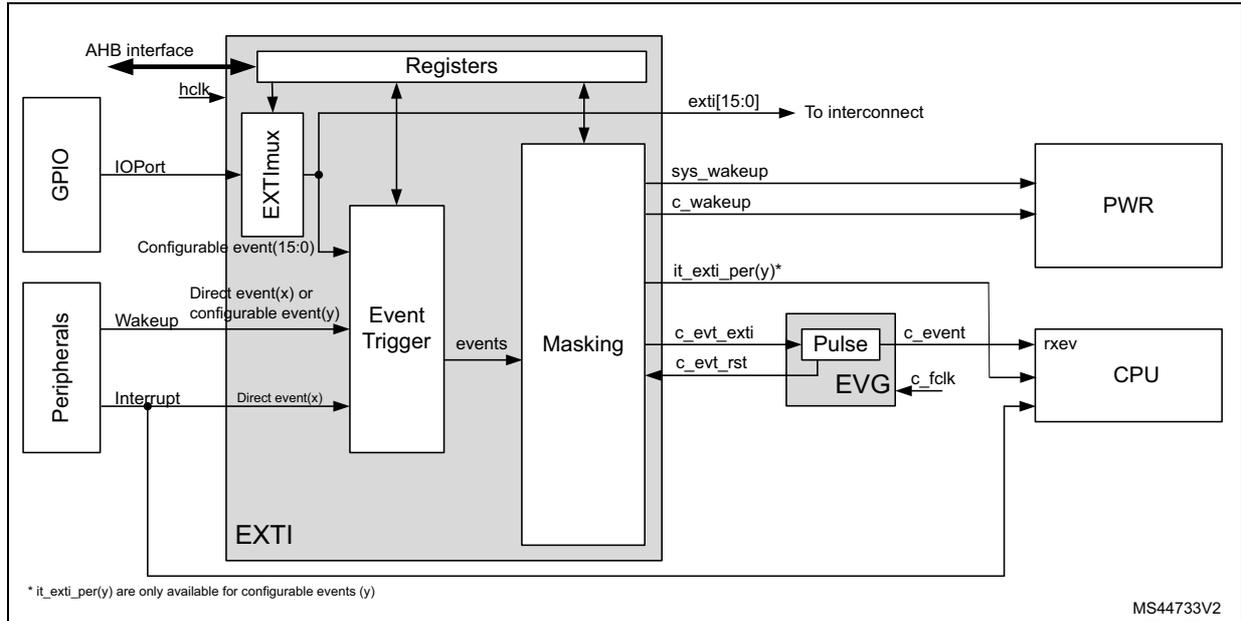
The diagram illustrates the internal architecture of the EXTI block. On the left, external blocks 'GPIO' and 'Peripherals' are connected. 'GPIO' connects via 'IOPort' to an 'EXTI mux'. 'Peripherals' connect via 'Wakeup' (Configurable event(15:0)) and 'Interrupt' (Direct event(x) or configurable event(y)) signals to an 'Event Trigger'. The 'Event Trigger' sends 'events' to a 'Masking' block. The 'Masking' block connects to a 'Pulse' block within an 'EVG' (Event Generator) unit. The 'EVG' unit also receives 'c_evt_rst' and 'c_fclk' signals and outputs 'c_event' and 'rxev' signals to a 'CPU' block. The 'CPU' block also receives 'it_exti_per(y)*' signals. The 'Registers' block is connected to an 'AHB interface' and 'hclk' signal, and it interfaces with the 'EXTI mux', 'Event Trigger', and 'Masking' block. The 'Registers' block also outputs 'exti[15:0]' to an external 'To interconnect' block, and 'sys_wakeup' and 'c_wakeup' signals to a 'PWR' (Power) block. A note at the bottom left states: '* it_exti_per(y) are only available for configurable events (y)'. The diagram is labeled 'MS44733V2' at the bottom right.
Table 62. EXTI signal overview
| Signal name | I/O | Description |
|---|---|---|
| AHB interface | I/O | EXTI register bus interface. When one event is configured to allow security, the AHB interface support secure accesses |
| hclk | I | AHB bus clock and EXTI system clock |
| Configurable event(y) | I | Asynchronous wake-up events from peripherals that do not have an associated interrupt and flag in the peripheral |
| Direct event(x) | I | Synchronous and asynchronous wake-up events from peripherals having an associated interrupt and flag in the peripheral |
| IOPort(n) | I | GPIO ports[15:0] |
| exti[15:0] | O | EXTI output port to trigger other IPs |
| it_exti_per (y) | O | Interrupts to the CPU associated with configurable event (y) |
| c_evt_exti | O | High-level sensitive event output for CPU synchronous to hclk |
| c_evt_rst | I | Asynchronous reset input to clear c_evt_exti |
| sys_wakeup | O | Asynchronous system wake-up request to PWR for ck_sys and hclk |
| c_wakeup | O | Wake-up request to PWR for CPU, synchronous to hclk |
Table 63. EVG pin overview
| Pin name | I/O | Description |
|---|---|---|
| c_fclk | I | CPU free-running clock |
| c_evt_in | I | High-level sensitive event input from EXTI, asynchronous to CPU clock |
| c_event | O | Event pulse, synchronous to CPU clock |
| c_evt_rst | O | Event reset signal, synchronous to CPU clock |
13.2.1 EXTI connections between peripherals and CPU
The peripherals able to generate wake-up or interrupt events when the system is in Stop mode are connected to the EXTI.
- • Peripheral wake-up signals that generate a pulse or that do not have an interrupt status bits in the peripheral, are connected to an EXTI configurable line. For these events the EXTI provides a status pending bit which requires to be cleared. It is the EXTI interrupt associated with the status bit that interrupts the CPU.
- • Peripheral interrupt and wake-up signals that have a status bit in the peripheral which requires to be cleared in the peripheral, are connected to an EXTI direct line. There is no status pending bit within the EXTI. The interrupt or wake-up is cleared by the CPU in the peripheral. It is the peripheral interrupt that interrupts the CPU directly.
- • All GPIO ports input to the EXTI multiplexer, allowing to select a port to wake up the system via a configurable event.
The EXTI configurable event interrupts are connected to the NVIC(a) of the CPU.
The dedicated EXTI/EVG CPU event is connected to the CPU rxev input.
The EXTI CPU wake-up signals are connected to the PWR block, and are used to wake up the system and CPU sub-system bus clocks.
13.3 EXTI functional description
Depending on the EXTI line type and wake-up target(s), different logic implementations are used. The applicable features and control or status registers are:
- • rising and falling edge event enable through
- – EXTI rising trigger selection register (EXTI_RTSR1)
- – EXTI falling trigger selection register 1 (EXTI_FTSR1)
- • software trigger through EXTI software interrupt event register 1 (EXTI_SWIER1)
- • pending interrupt flagging through
- – EXTI rising edge pending register 1 (EXTI_RPR1)
- – EXTI falling edge pending register 1 (EXTI_FPR1)
- – EXTI external interrupt selection register (EXTI_EXTICRx)
- • CPU wake-up and interrupt enable through
- – EXTI CPU wake-up with interrupt mask register (EXTI_IMR1)
- – EXTI CPU wake-up with interrupt mask register (EXTI_IMR2)
- • CPU wake-up and event enable through
- – EXTI CPU wake-up with event mask register (EXTI_EM1)
- – EXTI CPU wake-up with event mask register (EXTI_EM2)
Table 64. EXTI event input configurations and register control
| Event input type | Logic implementation | EXTI_RTSR1 | EXTI_FTSR1 | EXTI_SWIER1 | EXTI_R/FPR1 | EXTI_IMRx | EXTI_EM Rx |
|---|---|---|---|---|---|---|---|
| Configurable | Configurable event input wake-up logic | x | x | x | x | x | x |
| Direct | Direct event input wake-up logic | - | - | - | - | x | x |
13.3.1 EXTI configurable event input wake-up
Figure 27 is a detailed representation of the logic associated with configurable event inputs which wake up the CPU sub-system bus clocks and generated an EXTI pending flag and interrupt to the CPU and or a CPU wake-up event.
Figure 27. Configurable event trigger logic CPU wake-up
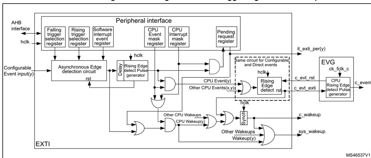
The software interrupt event register allows triggering configurable events by software, writing the corresponding register bit, irrespective of the edge selection setting.
The rising edge and falling edge selection registers allow to enable and select the configurable event active trigger edge or both edges.
The CPU has its dedicated interrupt mask register and a dedicated event mask registers. The enabled event allows generating an event on the CPU. All events for a CPU are OR-ed together into a single CPU event signal. The event pending registers (EXTI_RPR1 and EXTI_FPR1) is not set for an unmasked CPU event.
The configurable events have unique interrupt pending request registers, shared by the CPU. The pending register is only set for an unmasked interrupt. Each configurable event provides a common interrupt to the CPU. The configurable event interrupts need to be acknowledged by software in the EXTI_RPR1 and/or EXTI_FPR1 registers.
When a CPU interrupt or CPU event is enabled, the asynchronous edge detection circuit is reset by the clocked delay and rising edge detect pulse generator. This guarantees the wake-up of the EXTI hclk clock before the asynchronous edge detection circuit is reset.
Note: A detected configurable event interrupt pending request can be cleared by the CPU. The system cannot enter low-power modes as long as an interrupt pending request is active.
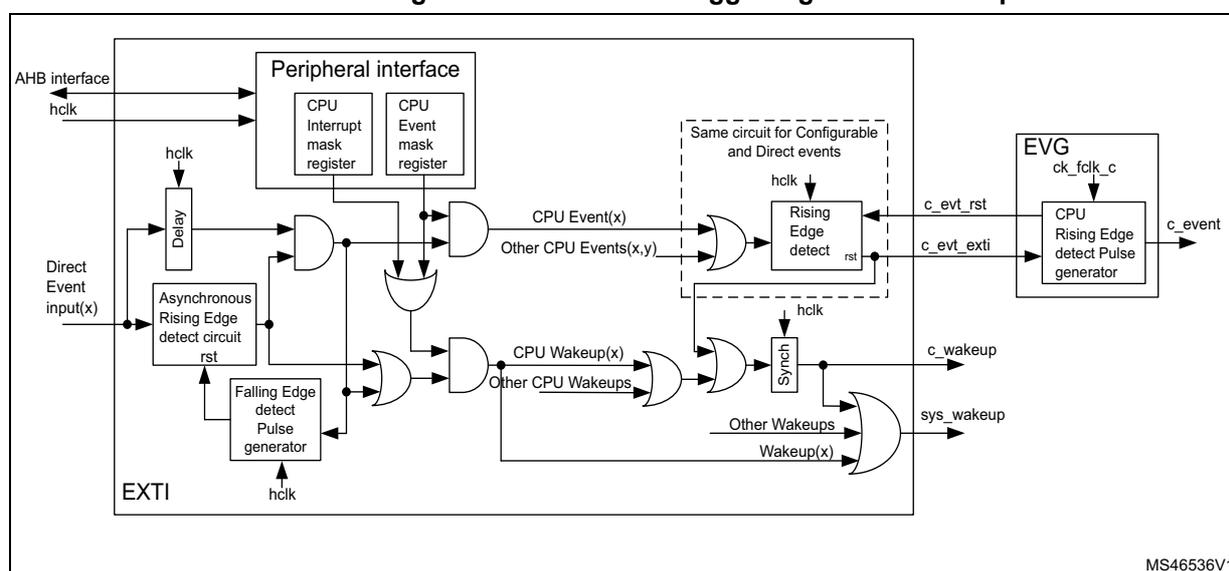
13.3.2 EXTI direct event input wake-up
Figure 28 is a detailed representation of the logic associated with direct event inputs waking up the system.
The direct events do not have an associated EXTI interrupt. The EXTI only wakes up the system and CPU sub-system clocks and may generate a CPU wake-up event. The peripheral synchronous interrupt, associated with the direct wake-up event wakes up the CPU.
The EXTI direct event is able to generate a CPU event. This CPU event wakes up the CPU. The CPU event may occur before the interrupt flag of the associated peripheral is set.
Figure 28. Direct event trigger logic CPU wake-up
13.3.3 EXTI mux
The EXTI mux allows selecting GPIOs as interrupts and wake-up. The GPIOs are connected via 16 EXTI mux lines to the first 16 EXTI events as configurable event. The selection of GPIO port as EXTI mux output is controlled through the EXTI external interrupt selection register (EXTI_EXTICRx) register.
Figure 29. EXTI GPIO mux
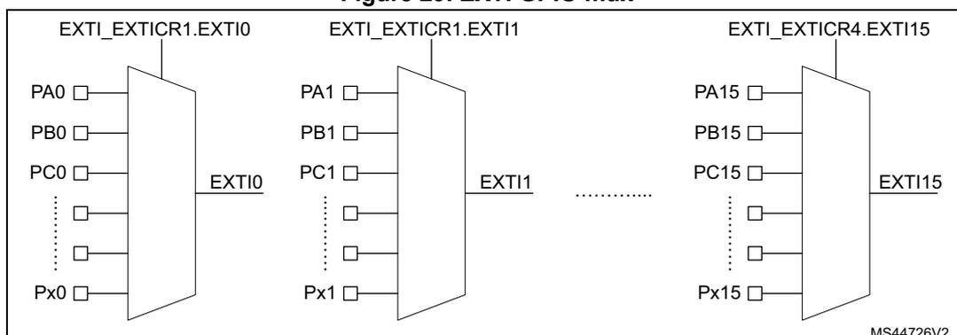
The diagram illustrates the EXTI GPIO multiplexers. It shows three separate multiplexers, each associated with a specific EXTI line. The first multiplexer, labeled EXTI_EXTICR1.EXTI10, selects between various GPIO pins (PA0, PB0, PC0, ..., Px0) to output the EXTI10 signal. The second multiplexer, labeled EXTI_EXTICR1.EXTI11, selects between pins (PA1, PB1, PC1, ..., Px1) to output the EXTI11 signal. The third multiplexer, labeled EXTI_EXTICR4.EXTI115, selects between pins (PA15, PB15, PC15, ..., Px15) to output the EXTI115 signal. Ellipses indicate additional pins and lines between the shown examples. A reference code MS44726V2 is present in the bottom right corner.
The EXTI mux outputs are available as output signals from the EXTI, to trigger other functional blocks. The EXTI mux outputs are available independently of mask setting through the EXTI_IMR and EXTI_EMR registers.
The EXTI lines (event inputs) are connected as shown in the following table.
Table 65. EXTI line connections
| EXTI line | Line source | Line type |
|---|---|---|
| 0-15 | GPIO | Configurable |
| 16 | PVD output | Configurable |
| 17 | COMP1 output | Configurable |
| 18 | COMP2 output | Configurable |
| 19 | RTC | Direct |
| 20 | COMP3 output | Configurable |
| 21 | TAMP | Direct |
| 22 | I2C2 wake-up | Direct |
| 23 | I2C1 wake-up | Direct |
| 24 | USART3 wake-up | Direct |
| 25 | USART1 wake-up | Direct |
| 26 | USART2 wake-up | Direct |
| 27 | CEC wake-up | Direct |
| 28 | LPUART1 wake-up | Direct |
| 29 | LPTIM1 | Direct |
| 30 | LPTIM2 | Direct |
| 31 | LSE_CSS | Direct |
| 32 | UCPD1 wake-up | Direct |
| 33 | UCPD2 wake-up | Direct |
| 34 | V DDIO2 monitoring | Configurable |
Table 65. EXTI line connections (continued)
| EXTI line | Line source | Line type |
|---|---|---|
| 35 | LPUART2 wake-up | Direct |
| 36 | USB wake-up | Direct |
13.4 EXTI functional behavior
The direct event inputs are enabled in the respective peripheral generating the wake-up event. The configurable events are enabled by enabling at least one of the trigger edges.
Once an event input is enabled, the generation of a CPU wake-up is conditioned by the CPU interrupt mask and CPU event mask.
Table 66. Masking functionality
| CPU interrupt enable EXTI_IMR.IMn | CPU event enable EXTI_EMR.EMn | Configurable event inputs EXTI_RPR.RPIFn EXTI_FPR.FPIFn | exti(n) interrupt (1) | CPU event | CPU wake-up |
|---|---|---|---|---|---|
| 0 | 0 | No | Masked | Masked | Masked |
| 1 | No | Masked | Yes | Yes | |
| 1 | 0 | Status latched | Yes | Masked | Yes (2) |
| 1 | Status latched | Yes | Yes | Yes |
- 1. The single exti(n) interrupt goes to the CPU. If no interrupt is required for CPU, the exti(n) interrupt must be masked in the CPU NVIC.
- 2. Only if CPU interrupt is enabled in EXTI_IMR.IMn.
For configurable event inputs, upon an edge on the event input, an event request is generated if that edge (rising or/and falling) is enabled. When the associated CPU interrupt is unmasked, the corresponding RPIFn and/or FPIFn bit is/are set in the EXTI_RPR or/and EXTI_FPR register, waking up the CPU subsystem and activating CPU interrupt signal. The RPIFn and/or FPIFn pending bit is cleared by writing 1 to it, which clears the CPU interrupt request.
For direct event inputs, when enabled in the associated peripheral, an event request is generated on the rising edge only. There is no corresponding CPU pending bit in the EXTI. When the associated CPU interrupt is unmasked, the corresponding CPU subsystem is woken up. The CPU is woken up (interrupted) by the peripheral synchronous interrupt.
The CPU event must be unmasked to generate an event. Upon an enabled edge occurring on an event input, a CPU event pulse is generated. There is no event pending bit.
For the configurable event inputs, the software can generate an event request by setting the corresponding bit of the software interrupt/event register EXTI_SWIER1, which has the effect of a rising edge on the event input. The pending rising edge event flag is set in the EXTI_RPR1 register, irrespective of the EXTI_RTSR1 register setting.
13.5 EXTI registers
The EXTI register map is divided in the following sections:
Table 67. EXTI register map sections
| Address | Description |
|---|---|
| 0x000 - 0x01C | General configurable event [31:0] configuration |
| 0x060 - 0x06C | EXTI I/O port multiplexer |
| 0x080 - 0x0BC | CPU input event configuration |
All the registers can be accessed with word (32-bit), half-word (16-bit) and byte (8-bit) access.
13.5.1 EXTI rising trigger selection register (EXTI_RTSR1)
Address offset: 0x000
Reset value: 0x0000 0000
Contains only register bits for configurable events.
| 31 | 30 | 29 | 28 | 27 | 26 | 25 | 24 | 23 | 22 | 21 | 20 | 19 | 18 | 17 | 16 |
| Res. | Res. | Res. | Res. | Res. | Res. | Res. | Res. | Res. | Res. | Res. | RT20 | Res. | RT18 | RT17 | RT16 |
| rw | rw | rw | rw | ||||||||||||
| 15 | 14 | 13 | 12 | 11 | 10 | 9 | 8 | 7 | 6 | 5 | 4 | 3 | 2 | 1 | 0 |
| RT15 | RT14 | RT13 | RT12 | RT11 | RT10 | RT9 | RT8 | RT7 | RT6 | RT5 | RT4 | RT3 | RT2 | RT1 | RT0 |
| rw | rw | rw | rw | rw | rw | rw | rw | rw | rw | rw | rw | rw | rw | rw | rw |
Bits 31:21 Reserved, must be kept at reset value.
Bit 20 RT20 : Rising trigger event configuration bit of configurable line 20 (1)
This bit enables/disables the rising edge trigger for the event and interrupt on the corresponding line.
0: Disable
1: Enable
The RT20 bit is only available in STM32G0B1xx and STM32G0C1xx. It is reserved in all the other devices.
Bit 19 Reserved, must be kept at reset value.
Bits 18:0 RTx : Rising trigger event configuration bit of configurable line x (x = 18 to 0) (1)
Each bit enables/disables the rising edge trigger for the event and interrupt on the corresponding line.
0: Disable
1: Enable
The RT18 and RT17 bits are reserved in STM32G031xx and STM32G041xx.
- 1. The configurable lines are edge triggered, no glitch must be generated on these inputs.
If a rising edge on the configurable line occurs during writing of the register, the associated pending bit is not set.
Rising edge trigger can be set for a line with falling edge trigger enabled. In this case, both edges generate a trigger.
13.5.2 EXTI falling trigger selection register 1 (EXTI_FTSR1)
Address offset: 0x004
Reset value: 0x0000 0000
Contains only register bits for configurable events.
| 31 | 30 | 29 | 28 | 27 | 26 | 25 | 24 | 23 | 22 | 21 | 20 | 19 | 18 | 17 | 16 |
|---|---|---|---|---|---|---|---|---|---|---|---|---|---|---|---|
| Res. | Res. | Res. | Res. | Res. | Res. | Res. | Res. | Res. | Res. | Res. | FT20 | Res. | FT18 | FT17 | FT16 |
| rw | rw | rw | rw | ||||||||||||
| 15 | 14 | 13 | 12 | 11 | 10 | 9 | 8 | 7 | 6 | 5 | 4 | 3 | 2 | 1 | 0 |
| FT15 | FT14 | FT13 | FT12 | FT11 | FT10 | FT9 | FT8 | FT7 | FT6 | FT5 | FT4 | FT3 | FT2 | FT1 | FT0 |
| rw | rw | rw | rw | rw | rw | rw | rw | rw | rw | rw | rw | rw | rw | rw | rw |
Bits 31:21 Reserved, must be kept at reset value.
Bit 20 FT20 : Falling trigger event configuration bit of configurable line 20 (1) .
This bit enables/disables the falling edge trigger for the event and interrupt on the corresponding line.
0: Disable
1: Enable
The FT20 bit is only available in STM32G0B1xx and STM32G0C1xx. It is reserved in all the other devices.
Bit 19 Reserved, must be kept at reset value.
Bits 18:0 FTx : Falling trigger event configuration bit of configurable line x (x = 18 to 0) (1) .
Each bit enables/disables the falling edge trigger for the event and interrupt on the corresponding line.
0: Disable
1: Enable
The FT18 and FT17 bits are reserved in STM32G031xx and STM32G041xx.
- 1. The configurable lines are edge triggered, no glitch must be generated on these inputs.
If a falling edge on the configurable line occurs during writing of the register, the associated pending bit is not set.
Falling edge trigger can be set for a line with rising edge trigger enabled. In this case, both edges generate a trigger.
13.5.3 EXTI software interrupt event register 1 (EXTI_SWIER1)
Address offset: 0x008
Reset value: 0x0000 0000
Contains only register bits for configurable events.
| 31 | 30 | 29 | 28 | 27 | 26 | 25 | 24 | 23 | 22 | 21 | 20 | 19 | 18 | 17 | 16 |
|---|---|---|---|---|---|---|---|---|---|---|---|---|---|---|---|
| Res. | Res. | Res. | Res. | Res. | Res. | Res. | Res. | Res. | Res. | Res. | SWI 20 | Res. | SWI 18 | SWI 17 | SWI 16 |
| rw | rw | rw | rw | ||||||||||||
| 15 | 14 | 13 | 12 | 11 | 10 | 9 | 8 | 7 | 6 | 5 | 4 | 3 | 2 | 1 | 0 |
| SWI 15 | SWI 14 | SWI 13 | SWI 12 | SWI 11 | SWI 10 | SWI9 | SWI8 | SWI7 | SWI6 | SWI5 | SWI4 | SWI3 | SWI2 | SWI1 | SWI0 |
| rw | rw | rw | rw | rw | rw | rw | rw | rw | rw | rw | rw | rw | rw | rw | rw |
Bits 31:21 Reserved, must be kept at reset value.
Bit 20 SWI20 : Software rising edge event trigger on line 20.
Setting this bit by software triggers a rising edge event on the corresponding line, resulting in an interrupt, independently of EXTI_RTSR1 and EXTI_FTSR1 settings. This bit is automatically cleared by hardware. Reading this bit always returns 0.
0: No effect
1: Rising edge event generated on the corresponding line, followed by an interrupt
The SWI20 bit is only available in STM32G0B1xx and STM32G0C1xx. It is reserved in all the other devices.
Bit 19 Reserved, must be kept at reset value.
Bits 18:0 SWIx : Software rising edge event trigger on line x (x = 18 to 0)
Setting of any bit by software triggers a rising edge event on the corresponding line x, resulting in an interrupt, independently of EXTI_RTSR1 and EXTI_FTSR1 settings. These bits are automatically cleared by HW. Reading of any bit always returns 0.
0: No effect
1: Rising edge event generated on the corresponding line, followed by an interrupt
The SWI18 and SWI17 bits are reserved in STM32G031xx and STM32G041xx.
13.5.4 EXTI rising edge pending register 1 (EXTI_RPR1)
Address offset: 0x00C
Reset value: 0x0000 0000
Contains only register bits for configurable events.
| 31 | 30 | 29 | 28 | 27 | 26 | 25 | 24 | 23 | 22 | 21 | 20 | 19 | 18 | 17 | 16 |
|---|---|---|---|---|---|---|---|---|---|---|---|---|---|---|---|
| Res. | Res. | Res. | Res. | Res. | Res. | Res. | Res. | Res. | Res. | Res. | RPIF20 | Res. | RPIF18 | RPIF17 | RPIF16 |
| rc_w1 | rc_w1 | rc_w1 | rc_w1 | ||||||||||||
| 15 | 14 | 13 | 12 | 11 | 10 | 9 | 8 | 7 | 6 | 5 | 4 | 3 | 2 | 1 | 0 |
| RPIF15 | RPIF14 | RPIF13 | RPIF12 | RPIF11 | RPIF10 | RPIF9 | RPIF8 | RPIF7 | RPIF6 | RPIF5 | RPIF4 | RPIF3 | RPIF2 | RPIF1 | RPIF0 |
| rc_w1 | rc_w1 | rc_w1 | rc_w1 | rc_w1 | rc_w1 | rc_w1 | rc_w1 | rc_w1 | rc_w1 | rc_w1 | rc_w1 | rc_w1 | rc_w1 | rc_w1 | rc_w1 |
Bits 31:21 Reserved, must be kept at reset value.
Bit 20 RPIF20 : Rising edge event pending for configurable line 20.
This bit is set upon a rising edge event generated by hardware or by software (through the EXTI_SWIER1 register) on the corresponding line. This bit is cleared by writing 1 into it.
0: No rising edge trigger request occurred
1: Rising edge trigger request occurred
The RPIF20 bit is only available in STM32G0B1xx and STM32G0C1xx. It is reserved in all the other devices.
Bit 19 Reserved, must be kept at reset value.
Bits 18:0 RPIFx : Rising edge event pending for configurable line x (x = 18 to 0)
Each bit is set upon a rising edge event generated by hardware or by software (through the EXTI_SWIER1 register) on the corresponding line. Each bit is cleared by writing 1 into it.
0: No rising edge trigger request occurred
1: Rising edge trigger request occurred
The RPIF18 and RPIF17 bits are reserved in STM32G031xx and STM32G041xx.
13.5.5 EXTI falling edge pending register 1 (EXTI_FPR1)
Address offset: 0x010
Reset value: 0x0000 0000
Contains only register bits for configurable events.
| 31 | 30 | 29 | 28 | 27 | 26 | 25 | 24 | 23 | 22 | 21 | 20 | 19 | 18 | 17 | 16 |
|---|---|---|---|---|---|---|---|---|---|---|---|---|---|---|---|
| Res. | Res. | Res. | Res. | Res. | Res. | Res. | Res. | Res. | Res. | Res. | FPIF20 | Res. | FPIF18 | FPIF17 | FPIF16 |
| rc_w1 | rc_w1 | rc_w1 | rc_w1 | ||||||||||||
| 15 | 14 | 13 | 12 | 11 | 10 | 9 | 8 | 7 | 6 | 5 | 4 | 3 | 2 | 1 | 0 |
| FPIF15 | FPIF14 | FPIF13 | FPIF12 | FPIF11 | FPIF10 | FPIF9 | FPIF8 | FPIF7 | FPIF6 | FPIF5 | FPIF4 | FPIF3 | FPIF2 | FPIF1 | FPIF0 |
| rc_w1 | rc_w1 | rc_w1 | rc_w1 | rc_w1 | rc_w1 | rc_w1 | rc_w1 | rc_w1 | rc_w1 | rc_w1 | rc_w1 | rc_w1 | rc_w1 | rc_w1 | rc_w1 |
Bits 31:21 Reserved, must be kept at reset value.
Bit 20 FPIF20 : Falling edge event pending for configurable line 20.
This bit is set upon a falling edge event generated by hardware on the corresponding line.
This bit is cleared by writing 1 into it.
0: No falling edge trigger request occurred
1: Falling edge trigger request occurred
The FPIF20 bit is only available in STM32G0B1xx and STM32G0C1xx. It is reserved in all the other devices.
Bit 19 Reserved, must be kept at reset value.
Bits 18:0 FPIFx : Falling edge event pending for configurable line x (x = 18 to 0)
Each bit is set upon a falling edge event generated by hardware on the corresponding line.
Each bit is cleared by writing 1 into it.
0: No falling edge trigger request occurred
1: Falling edge trigger request occurred
The FPIF18 and FPIF17 bits are reserved in STM32G031xx and STM32G041xx.
13.5.6 EXTI rising trigger selection register 2 (EXTI_RTSR2)
Address offset: 0x028
Reset value: 0x0000 0000
Contains only register bits for configurable events.
This register is not available in STM32G031xx and STM32G041xx, and in STM32G051xx and STM32G061xx.
| 31 | 30 | 29 | 28 | 27 | 26 | 25 | 24 | 23 | 22 | 21 | 20 | 19 | 18 | 17 | 16 |
|---|---|---|---|---|---|---|---|---|---|---|---|---|---|---|---|
| Res. | Res. | Res. | Res. | Res. | Res. | Res. | Res. | Res. | Res. | Res. | Res. | Res. | Res. | Res. | Res. |
| 15 | 14 | 13 | 12 | 11 | 10 | 9 | 8 | 7 | 6 | 5 | 4 | 3 | 2 | 1 | 0 |
| Res. | Res. | Res. | Res. | Res. | Res. | Res. | Res. | Res. | Res. | Res. | Res. | Res. | RT34 | Res. | Res. |
| rw | |||||||||||||||
Bits 31:3 Reserved, must be kept at reset value.
Bit 2 RT34 : Rising trigger event configuration bit of configurable line 34 (1)
This bit enables/disables the rising edge trigger for the event and interrupt on line 34.
0: Disable
1: Enable
This bit is only available in STM32G0B1xx and STM32G0C1xx. Reserved in all the other devices.
Bits 1:0 Reserved, must be kept at reset value.
- 1. The configurable lines are edge triggered, no glitch must be generated on these inputs.
If a rising edge on the configurable line occurs during writing of the register, the associated pending bit is not set.
Rising edge trigger can be set for a line with falling edge trigger enabled. In this case, both edges generate a trigger.
13.5.7 EXTI falling trigger selection register 2 (EXTI_FTSR2)
Address offset: 0x02C
Reset value: 0x0000 0000
Contains only register bits for configurable events.
This register is not available in STM32G031xx and STM32G041xx, and in STM32G051xx and STM32G061xx.
| 31 | 30 | 29 | 28 | 27 | 26 | 25 | 24 | 23 | 22 | 21 | 20 | 19 | 18 | 17 | 16 |
|---|---|---|---|---|---|---|---|---|---|---|---|---|---|---|---|
| Res. | Res. | Res. | Res. | Res. | Res. | Res. | Res. | Res. | Res. | Res. | Res. | Res. | Res. | Res. | Res. |
| 15 | 14 | 13 | 12 | 11 | 10 | 9 | 8 | 7 | 6 | 5 | 4 | 3 | 2 | 1 | 0 |
| Res. | Res. | Res. | Res. | Res. | Res. | Res. | Res. | Res. | Res. | Res. | Res. | Res. | FT34 | Res. | Res. |
| r/w |
Bits 31:3 Reserved, must be kept at reset value.
Bit 2 FT34 : Falling trigger event configuration bit of configurable line 34 (1) .
This bit enables/disables the falling edge trigger for the event and interrupt on the corresponding line.
0: Disable
1: Enable
This bit is only available in STM32G0B1xx and STM32G0C1xx. Reserved in all the other devices.
Bits 1:0 Reserved, must be kept at reset value.
- 1. The configurable lines are edge triggered, no glitch must be generated on these inputs.
If a falling edge on the configurable line occurs during writing of the register, the associated pending bit is not set.
Falling edge trigger can be set for a line with rising edge trigger enabled. In this case, both edges generate a trigger.
13.5.8 EXTI software interrupt event register 2 (EXTI_SWIER2)
Address offset: 0x030
Reset value: 0x0000 0000
Contains only register bits for configurable events.
This register is not available in STM32G031xx and STM32G041xx, and in STM32G051xx and STM32G061xx.
| 31 | 30 | 29 | 28 | 27 | 26 | 25 | 24 | 23 | 22 | 21 | 20 | 19 | 18 | 17 | 16 |
|---|---|---|---|---|---|---|---|---|---|---|---|---|---|---|---|
| Res. | Res. | Res. | Res. | Res. | Res. | Res. | Res. | Res. | Res. | Res. | Res. | Res. | Res. | Res. | Res. |
| 15 | 14 | 13 | 12 | 11 | 10 | 9 | 8 | 7 | 6 | 5 | 4 | 3 | 2 | 1 | 0 |
| Res. | Res. | Res. | Res. | Res. | Res. | Res. | Res. | Res. | Res. | Res. | Res. | Res. | SWI34 | Res. | Res. |
| nw |
Bits 31:3 Reserved, must be kept at reset value.
Bit 2 SWI34 : Software rising edge event trigger on line 34
Setting this bit by software triggers a rising edge event on the line 34, resulting in an interrupt, independently of EXTI_RTSR2 and EXTI_FTSR2 settings. This bit is automatically cleared by hardware. Reading this bit always returns 0.
0: No effect
1: Rising edge event generated on the line 34, followed by an interrupt
This bit is only available in STM32G0B1xx and STM32G0C1xx. Reserved in all the other devices.
Bits 1:0 Reserved, must be kept at reset value.
13.5.9 EXTI rising edge pending register 2 (EXTI_RPR2)
Address offset: 0x034
Reset value: 0x0000 0000
Contains only register bits for configurable events.
This register is not available in STM32G031xx and STM32G041xx, and in STM32G051xx and STM32G061xx.
| 31 | 30 | 29 | 28 | 27 | 26 | 25 | 24 | 23 | 22 | 21 | 20 | 19 | 18 | 17 | 16 |
|---|---|---|---|---|---|---|---|---|---|---|---|---|---|---|---|
| Res. | Res. | Res. | Res. | Res. | Res. | Res. | Res. | Res. | Res. | Res. | Res. | Res. | Res. | Res. | Res. |
| 15 | 14 | 13 | 12 | 11 | 10 | 9 | 8 | 7 | 6 | 5 | 4 | 3 | 2 | 1 | 0 |
| Res. | Res. | Res. | Res. | Res. | Res. | Res. | Res. | Res. | Res. | Res. | Res. | Res. | RPIF34 | Res. | Res. |
| rc_w1 |
Bits 31:3 Reserved, must be kept at reset value.
Bit 2 RPIF34 : Rising edge event pending for configurable line 34
This bit is set upon a rising edge event generated by hardware or by software (through the EXTI_SWIER2 register) on line 34. This bit is cleared by writing 1 into it.
0: No rising edge trigger request occurred
1: Rising edge trigger request occurred
This bit is only available in STM32G0B1xx and STM32G0C1xx. Reserved in all the other devices.
Bits 1:0 Reserved, must be kept at reset value.
13.5.10 EXTI falling edge pending register 2 (EXTI_FPR2)
Address offset: 0x038
Reset value: 0x0000 0000
Contains only register bits for configurable events.
This register is not available in STM32G031xx and STM32G041xx, and in STM32G051xx and STM32G061xx.
| 31 | 30 | 29 | 28 | 27 | 26 | 25 | 24 | 23 | 22 | 21 | 20 | 19 | 18 | 17 | 16 |
|---|---|---|---|---|---|---|---|---|---|---|---|---|---|---|---|
| Res. | Res. | Res. | Res. | Res. | Res. | Res. | Res. | Res. | Res. | Res. | Res. | Res. | Res. | Res. | Res. |
| 15 | 14 | 13 | 12 | 11 | 10 | 9 | 8 | 7 | 6 | 5 | 4 | 3 | 2 | 1 | 0 |
| Res. | Res. | Res. | Res. | Res. | Res. | Res. | Res. | Res. | Res. | Res. | Res. | Res. | FP1F34 | Res. | Res. |
| rc_w1 |
Bits 31:3 Reserved, must be kept at reset value.
Bit 2 FP1F34 : Falling edge event pending for configurable line 34
This bit is set upon a falling edge event generated by hardware on the line 34. This bit is cleared by writing 1 into it.
0: No falling edge trigger request occurred
1: Falling edge trigger request occurred
This bit is only available in STM32G0B1xx and STM32G0C1xx. Reserved in all the other devices.
Bits 1:0 Reserved, must be kept at reset value.
13.5.11 EXTI external interrupt selection register (EXTI_EXTICRx)
Address offset: 0x060 + 0x4 * (x - 1), (x = 1 to 4)
Reset value: 0x0000 0000
| 31 | 30 | 29 | 28 | 27 | 26 | 25 | 24 | 23 | 22 | 21 | 20 | 19 | 18 | 17 | 16 |
|---|---|---|---|---|---|---|---|---|---|---|---|---|---|---|---|
| EXTIm+3[7:0] | EXTIm+2[7:0] | ||||||||||||||
| rw | rw | rw | rw | rw | rw | rw | rw | rw | rw | rw | rw | rw | rw | rw | rw |
| 15 | 14 | 13 | 12 | 11 | 10 | 9 | 8 | 7 | 6 | 5 | 4 | 3 | 2 | 1 | 0 |
| EXTIm+1[7:0] | EXTIm[7:0] | ||||||||||||||
| rw | rw | rw | rw | rw | rw | rw | rw | rw | rw | rw | rw | rw | rw | rw | rw |
Bits 31:24 EXTIm+3[7:0] : EXTIm+3 GPIO port selection (m = 4 * (x - 1))
These bits are written by software to select the source input for EXTIm+3 external interrupt.
0x00: PA[m+3] pin
0x01: PB[m+3] pin
0x02: PC[m+3] pin
0x03: PD[m+3] pin
0x04: PE[m+3] pin
0x05: PF[m+3] pin
Other: Reserved
Bits 23:16 EXTIm+2[7:0] : EXTIm+2 GPIO port selection ( \( m = 4 * (x - 1) \) )
These bits are written by software to select the source input for EXTIm+2 external interrupt.
0x00: PA[m+2] pin
0x01: PB[m+2] pin
0x02: PC[m+2] pin
0x03: PD[m+2] pin
0x04: PE[m+2] pin
0x05: PF[m+2] pin
Other: Reserved
Bits 15:8 EXTIm+1[7:0] : EXTIm+1 GPIO port selection ( \( m = 4 * (x - 1) \) )
These bits are written by software to select the source input for EXTIm+1 external interrupt.
0x00: PA[m+1] pin
0x01: PB[m+1] pin
0x02: PC[m+1] pin
0x03: PD[m+1] pin
0x04: PE[m+1] pin
0x05: PF[m+1] pin
Other: Reserved
Bits 7:0 EXTIm[7:0] : EXTIm GPIO port selection ( \( m = 4 * (x - 1) \) )
These bits are written by software to select the source input for EXTIm external interrupt.
0x00: PA[m] pin
0x01: PB[m] pin
0x02: PC[m] pin
0x03: PD[m] pin
0x04: PE[m] pin
0x05: PF[m] pin
Other: Reserved
13.5.12 EXTI CPU wake-up with interrupt mask register (EXTI_IMR1)
Address offset: 0x080
Reset value: 0xFFF8 0000
Contains register bits for configurable events and direct events.
The reset value is set such as to, by default, enable interrupt from direct lines, and disable interrupt from configurable lines.
| 31 | 30 | 29 | 28 | 27 | 26 | 25 | 24 | 23 | 22 | 21 | 20 | 19 | 18 | 17 | 16 |
|---|---|---|---|---|---|---|---|---|---|---|---|---|---|---|---|
| IM31 | IM30 | IM29 | IM28 | IM27 | IM26 | IM25 | IM24 | IM23 | IM22 | IM21 | IM20 | IM19 | IM18 | IM17 | IM16 |
| rw | rw | rw | rw | rw | rw | rw | rw | rw | rw | rw | rw | rw | rw | rw | rw |
| 15 | 14 | 13 | 12 | 11 | 10 | 9 | 8 | 7 | 6 | 5 | 4 | 3 | 2 | 1 | 0 |
| IM15 | IM14 | IM13 | IM12 | IM11 | IM10 | IM9 | IM8 | IM7 | IM6 | IM5 | IM4 | IM3 | IM2 | IM1 | IM0 |
| rw | rw | rw | rw | rw | rw | rw | rw | rw | rw | rw | rw | rw | rw | rw | rw |
Bits 31:0 IMx : CPU wake-up with interrupt mask on line x (x = 31 to 0)
Setting/clearing each bit unmask/masks the CPU wake-up with interrupt, by an event on the corresponding line.
0: wake-up with interrupt masked
1: wake-up with interrupt unmasked
The IM24, IM22 and IM20 bits are only available in STM32G0B1xx and STM32G0C1xx.
They are reserved in all the other devices.
The IM27 bit is only available in STM32G071xx and STM32G081xx, and in STM32G0B1xx and STM32G0C1xx. It is reserved in all the other devices.
The IM18 and IM17 bits are reserved in STM32G031xx and STM32G041xx.
13.5.13 EXTI CPU wake-up with event mask register (EXTI_EMR1)
Address offset: 0x084
Reset value: 0x0000 0000
| 31 | 30 | 29 | 28 | 27 | 26 | 25 | 24 | 23 | 22 | 21 | 20 | 19 | 18 | 17 | 16 |
| EM31 | EM30 | EM29 | EM28 | EM27 | EM26 | EM25 | EM24 | EM23 | EM22 | EM21 | EM20 | EM19 | EM18 | EM17 | EM16 |
| rw | rw | rw | rw | rw | rw | rw | rw | rw | rw | rw | rw | rw | rw | rw | rw |
| 15 | 14 | 13 | 12 | 11 | 10 | 9 | 8 | 7 | 6 | 5 | 4 | 3 | 2 | 1 | 0 |
| EM15 | EM14 | EM13 | EM12 | EM11 | EM10 | EM9 | EM8 | EM7 | EM6 | EM5 | EM4 | EM3 | EM2 | EM1 | EM0 |
| rw | rw | rw | rw | rw | rw | rw | rw | rw | rw | rw | rw | rw | rw | rw | rw |
Bits 31:0 EMx : CPU wake-up with event generation mask on line x (x = 31 to 0)
Setting/clearing each bit unmask/masks the CPU wake-up with event generation on the corresponding line.
0: wake-up with event generation masked
1: wake-up with event generation unmasked
The EM24, EM22 and EM20 bits are only available in STM32G0B1xx and STM32G0C1xx.
They are reserved in all other devices.
The EM27 bit is only available in STM32G071xx and STM32G081xx, and STM32G0B1xx and STM32G0C1xx. It is reserved in all the other devices.
The EM18 and EM17 bits are reserved in STM32G031xx and STM32G041xx.
13.5.14 EXTI CPU wake-up with interrupt mask register (EXTI_IMR2)
Address offset: 0x090 (EXTI_IMR2)
Reset value: 0x0x0000 001B
Contains register bits for configurable events and direct events.
The reset value is set such as to, by default, enable interrupt from direct lines, and disable interrupt from configurable lines.
This register is not available in STM32G031xx and STM32G041xx, and in STM32G051xx and STM32G061xx.
| 31 | 30 | 29 | 28 | 27 | 26 | 25 | 24 | 23 | 22 | 21 | 20 | 19 | 18 | 17 | 16 |
|---|---|---|---|---|---|---|---|---|---|---|---|---|---|---|---|
| Res. | Res. | Res. | Res. | Res. | Res. | Res. | Res. | Res. | Res. | Res. | Res. | Res. | Res. | Res. | Res. |
| 15 | 14 | 13 | 12 | 11 | 10 | 9 | 8 | 7 | 6 | 5 | 4 | 3 | 2 | 1 | 0 |
| Res. | Res. | Res. | Res. | Res. | Res. | Res. | Res. | Res. | Res. | Res. | IM36 | IM35 | IM34 | IM33 | IM32 |
| rw | rw | rw | rw | rw |
Bits 31:5 Reserved, must be kept at reset value.
Bits 4:0 IMx : CPU wake-up with interrupt mask on line x (x = 36 to 32)
Setting/clearing this bit un.masks/masks the CPU wake-up with interrupt, by an event on the corresponding line.
0: wake-up with interrupt request from Line x is masked
1: wake-up with interrupt request from Line x is unmasked
The IM36, IM35, and IM34 bits are only available in STM32G0B1xx and STM32G0C1xx.
They are reserved in STM32G071xx and STM32G081xx.
13.5.15 EXTI CPU wake-up with event mask register (EXTI_EMR2)
Address offset: 0x094
Reset value: 0x0000 0000
Contains register bits for configurable events and direct events.
The reset value is set such as to, by default, enable interrupt from direct lines, and disable interrupt from configurable lines.
This register is not available in STM32G031xx and STM32G041xx, and in STM32G051xx and STM32G061xx.
| 31 | 30 | 29 | 28 | 27 | 26 | 25 | 24 | 23 | 22 | 21 | 20 | 19 | 18 | 17 | 16 |
|---|---|---|---|---|---|---|---|---|---|---|---|---|---|---|---|
| Res. | Res. | Res. | Res. | Res. | Res. | Res. | Res. | Res. | Res. | Res. | Res. | Res. | Res. | Res. | Res. |
| 15 | 14 | 13 | 12 | 11 | 10 | 9 | 8 | 7 | 6 | 5 | 4 | 3 | 2 | 1 | 0 |
| Res. | Res. | Res. | Res. | Res. | Res. | Res. | Res. | Res. | Res. | Res. | EM36 | EM35 | EM34 | EM33 | EM32 |
| rw | rw | rw | rw | rw |
Bits 31:5 Reserved, must be kept at reset value.
Bits 4:0 EMx : CPU wake-up with event generation mask on line x (x = 36 to 32)
Setting/clearing each bit un.masks/masks the CPU wake-up with event generation on the corresponding line.
0: wake-up with event generation masked
1: wake-up with event generation unmasked
The EM36, EM35, and EM34 bits are only available in STM32G0B1xx and STM32G0C1xx.
They are reserved in STM32G071xx and STM32G081xx.
13.5.16 EXTI register map
The following table gives the EXTI register map and the reset values.
Table 68. EXTI controller register map and reset values
| Offset | Register | 31 | 30 | 29 | 28 | 27 | 26 | 25 | 24 | 23 | 22 | 21 | 20 | 19 | 18 | 17 | 16 | 15 | 14 | 13 | 12 | 11 | 10 | 9 | 8 | 7 | 6 | 5 | 4 | 3 | 2 | 1 | 0 |
|---|---|---|---|---|---|---|---|---|---|---|---|---|---|---|---|---|---|---|---|---|---|---|---|---|---|---|---|---|---|---|---|---|---|
| 0x000 | EXTI_RTSR1 | Res. | Res. | Res. | Res. | Res. | Res. | Res. | Res. | Res. | Res. | Res. | RT20 | Res. | RT[18:0] | ||||||||||||||||||
| Reset value | 0 | 0 | 0 | 0 | 0 | 0 | 0 | 0 | 0 | 0 | 0 | 0 | 0 | 0 | 0 | 0 | 0 | 0 | 0 | 0 | |||||||||||||
| 0x004 | EXTI_FTSR1 | Res. | Res. | Res. | Res. | Res. | Res. | Res. | Res. | Res. | Res. | Res. | FT20 | Res. | FT[18:0] | ||||||||||||||||||
| Reset value | 0 | 0 | 0 | 0 | 0 | 0 | 0 | 0 | 0 | 0 | 0 | 0 | 0 | 0 | 0 | 0 | 0 | 0 | 0 | 0 | |||||||||||||
| 0x008 | EXTI_SWIER1 | Res. | Res. | Res. | Res. | Res. | Res. | Res. | Res. | Res. | Res. | Res. | SWI20 | Res. | SWI[18:0] | ||||||||||||||||||
| Reset value | 0 | 0 | 0 | 0 | 0 | 0 | 0 | 0 | 0 | 0 | 0 | 0 | 0 | 0 | 0 | 0 | 0 | 0 | 0 | 0 | |||||||||||||
| 0x00C | EXTI_RPR1 | Res. | Res. | Res. | Res. | Res. | Res. | Res. | Res. | Res. | Res. | Res. | RPIF20 | Res. | RPIF[18:0] | ||||||||||||||||||
| Reset value | 0 | 0 | 0 | 0 | 0 | 0 | 0 | 0 | 0 | 0 | 0 | 0 | 0 | 0 | 0 | 0 | 0 | 0 | 0 | 0 | |||||||||||||
| 0x010 | EXTI_FPR1 | Res. | Res. | Res. | Res. | Res. | Res. | Res. | Res. | Res. | Res. | Res. | FPIF20 | Res. | FPIF[16:0] Res. | ||||||||||||||||||
| Reset value | 0 | 0 | 0 | 0 | 0 | 0 | 0 | 0 | 0 | 0 | 0 | 0 | 0 | 0 | 0 | 0 | 0 | 0 | 0 | 0 | |||||||||||||
| 0x014- 0x024 | Reserved | Res. | Res. | Res. | Res. | Res. | Res. | Res. | Res. | Res. | Res. | Res. | Res. | Res. | Res. | Res. | Res. | Res. | Res. | Res. | Res. | Res. | Res. | Res. | Res. | Res. | Res. | Res. | Res. | Res. | Res. | Res. | Res. |
| 0x028 | EXTI_RTSR2 | Res. | Res. | Res. | Res. | Res. | Res. | Res. | Res. | Res. | Res. | Res. | Res. | Res. | Res. | Res. | Res. | Res. | Res. | Res. | Res. | Res. | Res. | Res. | Res. | Res. | Res. | Res. | Res. | Res. | RT34 | Res. | Res. |
| Reset value | 0 | ||||||||||||||||||||||||||||||||
| 0x02C | EXTI_FTSR2 | Res. | Res. | Res. | Res. | Res. | Res. | Res. | Res. | Res. | Res. | Res. | Res. | Res. | Res. | Res. | Res. | Res. | Res. | Res. | Res. | Res. | Res. | Res. | Res. | Res. | Res. | Res. | Res. | Res. | FT34 | Res. | Res. |
| Reset value | 0 | ||||||||||||||||||||||||||||||||
| 0x030 | EXTI_SWIER2 | Res. | Res. | Res. | Res. | Res. | Res. | Res. | Res. | Res. | Res. | Res. | Res. | Res. | Res. | Res. | Res. | Res. | Res. | Res. | Res. | Res. | Res. | Res. | Res. | Res. | Res. | Res. | Res. | Res. | SWI34 | Res. | Res. |
| Reset value | 0 | ||||||||||||||||||||||||||||||||
| 0x034 | EXTI_RPR2 | Res. | Res. | Res. | Res. | Res. | Res. | Res. | Res. | Res. | Res. | Res. | Res. | Res. | Res. | Res. | Res. | Res. | Res. | Res. | Res. | Res. | Res. | Res. | Res. | Res. | Res. | Res. | Res. | Res. | RPIF34 | Res. | Res. |
| Reset value | 0 | ||||||||||||||||||||||||||||||||
| 0x038 | EXTI_FPR2 | Res. | Res. | Res. | Res. | Res. | Res. | Res. | Res. | Res. | Res. | Res. | Res. | Res. | Res. | Res. | Res. | Res. | Res. | Res. | Res. | Res. | Res. | Res. | Res. | Res. | Res. | Res. | Res. | Res. | FPIF34 | Res. | Res. |
| Reset value | 0 | ||||||||||||||||||||||||||||||||
| 0x038- 0x05C | Reserved | Res. | Res. | Res. | Res. | Res. | Res. | Res. | Res. | Res. | Res. | Res. | Res. | Res. | Res. | Res. | Res. | Res. | Res. | Res. | Res. | Res. | Res. | Res. | Res. | Res. | Res. | Res. | Res. | Res. | Res. | Res. | Res. |
| 0x060 | EXTI_EXTICR1 | EXTI3[7:0] | EXTI2[7:0] | EXTI1[7:0] | EXTI0[7:0] | ||||||||||||||||||||||||||||
| Reset value | 0 | 0 | 0 | 0 | 0 | 0 | 0 | 0 | 0 | 0 | 0 | 0 | 0 | 0 | 0 | 0 | 0 | 0 | 0 | 0 | 0 | 0 | 0 | 0 | 0 | 0 | 0 | 0 | 0 | 0 | 0 | 0 | |
| 0x064 | EXTI_EXTICR2 | EXTI7[7:0] | EXTI6[7:0] | EXTI5[7:0] | EXTI4[7:0] | ||||||||||||||||||||||||||||
| Reset value | 0 | 0 | 0 | 0 | 0 | 0 | 0 | 0 | 0 | 0 | 0 | 0 | 0 | 0 | 0 | 0 | 0 | 0 | 0 | 0 | 0 | 0 | 0 | 0 | 0 | 0 | 0 | 0 | 0 | 0 | 0 | 0 | |
| 0x068 | EXTI_EXTICR3 | EXTI11[7:0] | EXTI10[7:0] | EXTI9[7:0] | EXTI8[7:0] | ||||||||||||||||||||||||||||
| Reset value | 0 | 0 | 0 | 0 | 0 | 0 | 0 | 0 | 0 | 0 | 0 | 0 | 0 | 0 | 0 | 0 | 0 | 0 | 0 | 0 | 0 | 0 | 0 | 0 | 0 | 0 | 0 | 0 | 0 | 0 | 0 | 0 | |
Table 68. EXTI controller register map and reset values (continued)
| Offset | Register | 31 | 30 | 29 | 28 | 27 | 26 | 25 | 24 | 23 | 22 | 21 | 20 | 19 | 18 | 17 | 16 | 15 | 14 | 13 | 12 | 11 | 10 | 9 | 8 | 7 | 6 | 5 | 4 | 3 | 2 | 1 | 0 |
|---|---|---|---|---|---|---|---|---|---|---|---|---|---|---|---|---|---|---|---|---|---|---|---|---|---|---|---|---|---|---|---|---|---|
| 0x06C | EXTI_EXTICR4 | EXTI15[7:0] | EXTI14[7:0] | EXTI13[7:0] | EXTI12[7:0] | ||||||||||||||||||||||||||||
| Reset value | 0 | 0 | 0 | 0 | 0 | 0 | 0 | 0 | 0 | 0 | 0 | 0 | 0 | 0 | 0 | 0 | 0 | 0 | 0 | 0 | 0 | 0 | 0 | 0 | 0 | 0 | 0 | 0 | 0 | 0 | 0 | 0 | |
| 0x070- 0x07C | Reserved | Res | Res | Res | Res | Res | Res | Res | Res | Res | Res | Res | Res | Res | Res | Res | Res | Res | Res | Res | Res | Res | Res | Res | Res | Res | Res | Res | Res | Res | Res | Res | Res |
| 0x080 | EXTI_IMR1 | IM[31:0] | |||||||||||||||||||||||||||||||
| Reset value | 1 | 1 | 1 | 1 | 1 | 1 | 1 | 1 | 1 | 1 | 0 | 0 | 0 | 0 | 0 | 0 | 0 | 0 | 0 | 0 | 0 | 0 | 0 | 0 | 0 | 0 | 0 | 0 | |||||
| 0x084 | EXTI_EMR1 | EM[31:0] | |||||||||||||||||||||||||||||||
| Reset value | 0 | 0 | 0 | 0 | 0 | 0 | 0 | 0 | 0 | 0 | 0 | 0 | 0 | 0 | 0 | 0 | 0 | 0 | 0 | 0 | 0 | 0 | 0 | 0 | 0 | 0 | 0 | 0 | 0 | 0 | 0 | ||
| 0x088- 0x08C | Reserved | Res | Res | Res | Res | Res | Res | Res | Res | Res | Res | Res | Res | Res | Res | Res | Res | Res | Res | Res | Res | Res | Res | Res | Res | Res | Res | Res | Res | Res | Res | Res | Res |
| 0x090 | EXTI_IMR2 | Res | Res | Res | Res | Res | Res | Res | Res | Res | Res | Res | Res | Res | Res | Res | Res | Res | Res | Res | Res | Res | Res | Res | Res | Res | Res | Res | Res | IM36 | IM35 | IM34 | IM33 |
| Reset value | 1 | 1 | 1 | 1 | |||||||||||||||||||||||||||||
| 0x094 | EXTI_EMR2 | Res | Res | Res | Res | Res | Res | Res | Res | Res | Res | Res | Res | Res | Res | Res | Res | Res | Res | Res | Res | Res | Res | Res | Res | Res | Res | Res | Res | EM36 | EM35 | EM34 | EM33 |
| Reset value | 0 | 0 | 0 | 0 | |||||||||||||||||||||||||||||
Refer to Section 2.2 on page 60 for the register boundary addresses.