3. Embedded flash memory (FLASH)
3.1 FLASH Introduction
The flash memory interface manages CPU (Cortex®-M0+) AHB accesses to the flash memory. It implements erase and program flash memory operations, read and write protection, and security mechanisms.
The flash memory interface accelerates code execution with a system of instruction prefetch and cache lines.
3.2 FLASH main features
- • Up to 512 Kbytes of flash memory (main memory):
- – up to 64 Kbytes for STM32G031xx and STM32G041xx / STM32G051xx and STM32G061xx
- – up to 128 Kbytes for STM32G071xx and STM32G081xx
- – up to 512 Kbytes for STM32G0B1xx and STM32G0C1xx
- • Memory organization:
- – 1 bank (devices with up to 128 Kbytes of flash memory)
- – 2 banks (devices with more than 128 Kbytes of flash memory)
- – Page size: 2 Kbytes
- – Subpage size: 512 bytes
- • 72-bit wide data read (64 bits plus 8 ECC bits)
- • 72-bit wide data write (64 bits plus 8 ECC bits)
- • Page erase (2 Kbytes), bank (single-bank) erase, and mass (all-bank) erase
Flash memory interface features:
- • Flash memory read operations
- • Flash memory program/erase operations
- • Read protection activated by option (RDP)
- • Two write protection areas per bank, selected by option (WRP)
- • Two proprietary code read protection areas per bank, selected by option (PCROP)
- • Securable memory area
- • Flash memory empty check
- • Prefetch buffer
- • CPU instruction cache: two cache lines of 64 bits (16 bytes RAM)
- • Error code correction (ECC): eight bits for 64 bits
- • Option byte loader
3.3 FLASH functional description
3.3.1 FLASH organization
The flash memory is organized as 72-bit-wide memory cells (64 bits plus 8 ECC bits) that can be used for storing both code and data constants.
The flash memory is organized as follows:
- • A main memory block divided into one or two banks of up to 128 pages of 2 Kbytes each, with eight rows of 256 bytes in each page
- • An information block containing:
- – System memory from which the CPU boots in system memory boot mode. The area is reserved and contains the bootloader used to reprogram the flash memory through one of the interfaces listed in the Section 2.5.2: Embedded bootloader . On the manufacturing line, the devices are programmed and protected against spurious write/erase operations. For further details, refer to the AN2606 available from www.st.com .
- – 1 Kbyte (128 double words) OTP (one-time programmable) for user data. The OTP data cannot be erased and can be written only once. Once written, the entire double word cannot be written anymore, even with the value 0x0000 0000 0000 0000.
- – Option bytes for user configuration.
The following tables show the mapping of the flash memory into information block and main memory area.
Table 9. Flash memory organization for single-bank devices
| Area | Addresses | Size (bytes) | 16 KB devices | 32 KB devices | 64 KB devices | 128 KB devices | 256 KB devices (1) |
|---|---|---|---|---|---|---|---|
| Information block | 0x1FFF 7800 - 0x1FFF 787F | 128 | Option bytes | ||||
| 0x1FFF 7500 - 0x1FFF 77FF | 768 | Engineering bytes | |||||
| 0x1FFF 7000 - 0x1FFF 73FF | 1 K | OTP area | |||||
| 0x1FFF 2000 - 0x1FFF 6FFF | 20 K | - | System memory | ||||
| 0x1FFF 0000 - 0x1FFF 1FFF | 8 K | System memory | |||||
Table 9. Flash memory organization for single-bank devices (continued)
| Area | Addresses | Size (bytes) | 16 KB devices | 32 KB devices | 64 KB devices | 128 KB devices | 256 KB devices (1) |
|---|---|---|---|---|---|---|---|
| Main memory (Bank 1) | 0x0803 F800 - 0x0803 FFFF | 2 K | Page 127 | ||||
| ... | ... | ... | |||||
| 0x0801 F800 - 0x0801 FFFF | 2 K | Page 63 | |||||
| ... | ... | ... | |||||
| 0x0800 F800 - 0x0800 FFFF | 2 K | Page 31 | |||||
| ... | ... | ... | |||||
| 0x0800 7800 - 0x0800 7FFF | 2 K | Page 15 | |||||
| ... | ... | ... | |||||
| 0x0800 3800 - 0x0800 3FFF | 2 K | Page 7 | |||||
| ... | ... | ... | |||||
| 0x0800 0800 - 0x0800 0FFF | 2 K | Page 1 | |||||
| 0x0800 0000 - 0x0800 07FF | 2 K | Page 0 |
1. Flash memory configured in single-bank mode, by clearing the DUAL_BANK option bit.
The following table shows the flash memory organization of the 256 KB device when its flash memory is configured in dual-bank mode, by setting the DUAL_BANK option bit.
Table 10. Flash memory organization for 256 KB dual-bank devices
| Area | Addresses | Size (bytes) | Memory type |
|---|---|---|---|
| Information block | 0x1FFF 7800 - 0x1FFF 787F | 128 | Option bytes |
| 0x1FFF 7500 - 0x1FFF 77FF | 768 | Engineering bytes | |
| 0x1FFF 7000 - 0x1FFF 73FF | 1 K | OTP area | |
| 0x1FFF 0000 - 0x1FFF 6FFF | 28 K | System memory | |
| Main memory | 0x0803 F800 - 0x0803 FFFF | 2 K | Page 63 |
| ... | ... | ... | |
| 0x0802 0800 - 0x0802 0FFF | 2 K | Page 1 | |
| 0x0802 0000 - 0x0802 07FF | 2 K | Page 0 | |
| 0x0801 F800 - 0x0801 FFFF | 2 K | Page 63 | |
| ... | ... | ... | |
| 0x0800 0800 - 0x0800 0FFF | 2 K | Page 1 | |
| 0x0800 0000 - 0x0800 07FF | 2 K | Page 0 |
1. If the banks are swapped (see nSWAP_BANK option bit description), the bank 2 is addressed as the memory range 0x0800 0000 - 0x0801 FFFF and the bank 1 as 0x0802 0000 - 0x0803 FFFF.
Table 11. Flash memory organization for 512 KB devices
| Area | Addresses | Size (bytes) | Memory type | |
|---|---|---|---|---|
| Information block | Bank 1 | 0x1FFF 7800 - 0x1FFF 787F | 128 | Option bytes |
| 0x1FFF 7500 - 0x1FFF 77FF | 768 | Engineering bytes | ||
| 0x1FFF 7000 - 0x1FFF 73FF | 1 K | OTP area | ||
| 0x1FFF 0000 - 0x1FFF 6FFF | 28 K | System memory | ||
| Main memory | Bank 2 (1) | 0x0807 F800 - 0x0807 FFFF | 2 K | Page 127 |
| ... | ... | ... | ||
| 0x0804 0800 - 0x0804 0FFF | 2 K | Page 1 | ||
| 0x0804 0000 - 0x0804 07FF | 2 K | Page 0 | ||
| Bank 1 (1) | 0x0803 F800 - 0x0803 FFFF | 2 K | Page 127 | |
| ... | ... | ... | ||
| 0x0800 0800 - 0x0800 0FFF | 2 K | Page 1 | ||
| 0x0800 0000 - 0x0800 07FF | 2 K | Page 0 | ||
1. If the banks are swapped (see nSWAP_BANK option bit description), the bank 2 is addressed as the memory range 0x0800 0000 - 0x0803 FFFF and the bank 1 as 0x0804 0000 - 0x0807 FFFF.
3.3.2 FLASH dual-bank capability
The STM32G0B1xx and STM32G0C1xx devices support dual-bank flash memory capability. This feature allows using the read-while-write (RWW) function. It is also possible to swap, by hardware, the logical address mapping of the physical flash memory banks. The dual-bank and the bank swap functions are controlled with the DUAL_BANK and nSWAP_BANK option bits, respectively.
Table 12. Flash memory bank mapping
| Device flash size | DUAL_BANK | Flash mode | nSWAP_BANK | Address mapping |
|---|---|---|---|---|
| 512 Kbytes | X (1) | Dual-bank | 1 | Bank 1: 0x0800 0000 – 0x0803 FFFF |
| Bank 2: 0x0804 0000 – 0x0807 FFFF | ||||
| 0 | Bank 1: 0x0804 0000 – 0x0807 FFFF | |||
| Bank 2: 0x0800 0000 – 0x0803 FFFF | ||||
| 256 Kbytes | 1 | Dual-bank | 1 | Bank 1: 0x0800 0000 – 0x0801 FFFF |
| Bank 2: 0x0802 0000 – 0x0803 FFFF | ||||
| 0 | Bank 1: 0x0802 0000 – 0x0803 FFFF | |||
| Bank 2: 0x0800 0000 – 0x0801 FFFF | ||||
| 128 Kbytes and less | 0 | Single-bank | X (2) | Bank 1: 0x0800 0000 – 0x0803 FFFF |
| Bank 2: not available | ||||
| 128 Kbytes and less | X (3) or N/A | Single-bank | X (2) or N/A | Bank 1: 0x0800 0000 – 0x0801 FFFF |
| Bank 2: not available |
- 1. The 512 Kbyte device always operates in dual-bank mode.
- 2. nSWAP_BANK has no effect when the device is configured in single-bank mode.
- 3. The 128 Kbyte device always operates in single-bank mode.
Flash memory programming
The flash memory programming is always performed at a specified logical address in the flash memory range. The hardware automatically performs the programming sequence in the right bank following the remapping shown in Table 12: Flash memory bank mapping . Consequently, no specific sequence is required, regardless of the flash memory mode and bank swapping used.
Flash memory erasing
The flash memory erase operation can be performed at page level (page erase) or bank level (mass erase). As shown in Section 3.3.7: FLASH main memory erase sequences , the erase operation is always linked to a specific physical flash memory bank (that is, bank 1 or bank 2). Consequently, the erase or mass erase operation is not affected by the nSWAP_BANK option bit.
Flash memory write protection
The flash memory write protection configuration in the option bytes is also linked with physical flash banks. Therefore, care must be taken to select WRP1 or WRP2, depending on the nSWAP_BANK configuration.
3.3.3 FLASH error code correction (ECC)
Data in flash memory words are 72-bits wide: eight bits are added per each double word (64 bits). The ECC mechanism supports:
- • One error detection and correction
- • Two errors detection
When one error is detected and corrected, the flag ECCC (ECC correction) is set in FLASH ECC register (FLASH_ECCR) or in FLASH ECC register 2 (FLASH_ECCR2) for error in bank 2. If ECCCIE is set, an interrupt is generated.
When two errors are detected, a flag ECCD (ECC detection) is set in FLASH ECC register (FLASH_ECCR) . In this case, a NMI is generated.
When an ECC error is detected, the address of the failing double word is saved in ADDR_ECC[15:0] bitfield of the FLASH_ECCR register. ADDR_ECC[2:0] are always cleared.
While ECCC or ECCD is set, FLASH_ECCR is not updated if a new ECC error occurs. FLASH_ECCR is updated only when ECC flags are cleared.
Note: For a virgin data: 0xFF FFFF FFFF FFFF FFFF, one error is detected and corrected, but two errors detection is not supported.
When an ECC error is reported, a new read at the failing address may not generate an ECC error if the data is still present in the current buffer, even if ECCC and ECCD are cleared. If this is not the desired behavior, the user must reset the cache.
The ECC status for the bank 2 is reported in FLASH ECC register 2 (FLASH_ECCR2) .
3.3.4 FLASH read access latency
To correctly read data from flash memory, the number of wait states (LATENCY) must be correctly programmed in the FLASH access control register (FLASH_ACR) according to the frequency of the flash memory clock (HCLK) and the internal voltage range of the device \( V_{CORE} \) . Refer to Section 4.1.4: Dynamic voltage scaling management . Table 13 shows the correspondence between wait states and flash memory clock frequency.
Table 13. Number of wait states according to flash memory clock (HCLK) frequency
| Wait states (WS) (LATENCY) | HCLK (MHz) | |
|---|---|---|
| \( V_{CORE} \) Range 1 | \( V_{CORE} \) Range 2 | |
| 0 WS (1 HCLK cycles) | \( \leq 24 \) | \( \leq 8 \) |
| 1 WS (2 HCLK cycles) | \( \leq 48 \) | \( \leq 16 \) |
| 2 WS (3 HCLK cycles) | \( \leq 64 \) | - |
After power reset, the HCLK clock frequency is 16 MHz in Range 1 and 0 wait state (WS) is configured in the FLASH_ACR register.
When waking up from Standby, the HCLK clock frequency is 16 MHz in Range 1 and 0 wait state (WS) is configured in the FLASH_ACR register.
When changing the flash memory clock frequency or Range, the following software sequences must be applied in order to tune the number of wait states needed to access the flash memory:
Increasing the CPU frequency
- 1. Program the new number of wait states to the LATENCY bits of the FLASH access control register (FLASH_ACR) .
- 2. Check that the new number of wait states is taken into account to access the flash memory by reading back the LATENCY bits of the FLASH access control register (FLASH_ACR) , and wait until the programmed new number is read.
- 3. Modify the system clock source by writing the SW bits of the RCC_CFGR register.
- 4. If needed, modify the core clock prescaler by writing the HPRE bits of RCC_CFGR register.
- 5. Optionally, check that the new system clock source or/and the new core clock prescaler value is/are taken into account by reading the clock source status (SWS bits) of the RCC_CFGR register, or/and the AHB prescaler value (HPREF bit), of the RCC_CFGR register.
Decreasing the CPU frequency
- 1. Modify the system clock source by writing the SW bits of the RCC_CFGR register.
- 2. If needed, modify the core clock prescaler by writing the HPRE bits of RCC_CFGR.
- 3. Check that the new system clock source or/and the new core clock prescaler value is/are taken into account by reading the clock source status (SWS bits) of the RCC_CFGR register, or/and the AHB prescaler value (HPREF bit), of the RCC_CFGR register.
- register, and wait until the programmed new system clock source or/and new flash memory clock prescaler value is/are read.
- 4. Program the new number of wait states to the LATENCY bits of the FLASH access control register (FLASH_ACR) .
- 5. Optionally, check that the new number of wait states is used to access the flash memory by reading back the LATENCY bits of the FLASH access control register (FLASH_ACR) .
3.3.5 FLASH memory acceleration
Instruction prefetch
Each flash memory read operation provides 64 bits from either two instructions of 32 bits or four instructions of 16 bits according to the program launched. This 64-bits current instruction line is saved in a current buffer. So, in case of sequential code, at least two CPU cycles are needed to execute the previous read instruction line. Prefetch on the CPU S-bus can be used to read the next sequential instruction line from the flash memory while the current instruction line is being requested by the CPU.
Prefetch is enabled by setting the PRFTEN bit of the FLASH access control register (FLASH_ACR) . This feature is useful if at least one wait state is needed to access the flash memory.
When the code is not sequential (branch), the instruction may not be present in the currently used instruction line or in the prefetched instruction line. In this case (miss), the penalty in terms of number of cycles is at least equal to the number of wait states.
If a loop is present in the current buffer, no new access is performed.
Caution: In rare cases, the instruction prefetch may fail upon transiting across flash memory banks. Therefore, it is mandatory to temporarily disable the instruction prefetch when the application code branches or does function calls from one flash memory bank to the other (in dual-bank flash memory configuration). Refer to the corresponding product errata sheet for more details on this limitation.
Cache memory
To limit the time lost due to jumps, it is possible to retain two cache lines of 64 bits (16 bytes) in the instruction cache memory. This feature can be enabled by setting the instruction cache enable (ICEN) bit of the FLASH access control register (FLASH_ACR) . Each time a miss occurs (requested data not present in the currently used instruction line, in the prefetched instruction line or in the instruction cache memory), the line read is copied into the instruction cache memory. If some data contained in the instruction cache memory are requested by the CPU, they are provided without inserting any delay. Once all the instruction cache memory lines are filled, the LRU (least recently used) policy is used to determine the line to replace in the instruction memory cache. This feature is particularly useful in case of code containing loops.
The Instruction cache memory is enabled after system reset.
No data cache is available on Cortex ® -M0+.
3.3.6 FLASH program and erase operations
The device-embedded flash memory can be programmed using in-circuit programming or in-application programming.
The in-circuit programming (ICP) method is used to update the entire contents of the flash memory, using SWD protocol or the supported interfaces by the system bootloader, to load the user application for the CPU, into the microcontroller. ICP offers quick and efficient design iterations and eliminates unnecessary package handling or socketing of devices.
In contrast to the ICP method, in-application programming (IAP) can use any communication interface supported by the microcontroller (I/Os, UART, I 2 C, SPI, etc.) to download programming data into memory. IAP allows the user to re-program the flash memory while the application is running. Nevertheless, part of the application has to have been previously programmed in the flash memory using ICP.
The success of a data word programming operation and a page/bank erase operation is not guaranteed if aborted due to device reset or power loss.
Caution: Due to the structure of the flash memory (64 bits of data with associated 8 bits of ECC), any ongoing program or erase memory operation interrupted by a physical phenomena such as reset or power-off might result in a corrupted flash memory data and/or ECC bits. The address concerned might trigger an ECC interrupt or an NMI when accessed later on. Consequently, it is important that the firmware always handles flash memory program and erase operations with care and that it manages ECC events.
During a program/erase operation in the flash memory, any attempt to read the flash memory stalls the bus. The read operation proceeds correctly once the program/erase operation has completed.
Unlocking the flash memory
After reset, write into the FLASH control register (FLASH_CR) is not allowed so as to protect the flash memory against possible unwanted operations due, for example, to electric disturbances. The following sequence unlocks these registers:
- 1. Write KEY1 = 0x4567 0123 in the FLASH key register (FLASH_KEYR)
- 2. Write KEY2 = 0xCDEF 89AB in the FLASH key register (FLASH_KEYR) .
Any wrong sequence locks the FLASH_CR register until the next system reset. In the case of a wrong key sequence, a bus error is detected and a Hard Fault interrupt is generated.
The FLASH_CR register can be locked again by software, by setting its LOCK bit.
Note: The FLASH_CR register cannot be written when the BSY1 or the BSY2 bit of the FLASH status register (FLASH_SR) is set. Any attempt to write to this register with the BSY1 or the BSY2 bit set causes the AHB bus to stall until both bits are cleared.
3.3.7 FLASH main memory erase sequences
The flash memory erase operation can be performed at page level (page erase), or on the whole memory (mass erase). Mass erase does not affect the Information block (system flash memory, OTP and option bytes).
Flash memory page erase
When a page is protected by PCROP or WRP, it is not erased and the WRPERR bit is set.
Table 14. Page erase overview
| SEC_PROT | PCROP | WRP | PCROP_RDP | Comment | WRPERR | CPU bus error |
|---|---|---|---|---|---|---|
| 0 | No | No | x | Page is erased | No | No |
| No | Yes | Page erase aborted (no page erase started) | Yes | |||
| Yes | No | |||||
| Yes | Yes | |||||
| 1 | x | Protected pages only | No | Yes | ||
To erase a page (2 Kbytes), proceed as follows:
- 1. Check that no flash memory operation is ongoing on the targeted bank, by checking the BSY1 or BSY2 bit of the FLASH status register (FLASH_SR) .
- 2. Check and clear all error programming flags due to a previous programming. If not, PGSERR is set.
- 3. Check that CFGBSY is cleared.
- 4. Set the PER bit and select the page to erase (BKER, PNB) in the FLASH control register (FLASH_CR) .
- 5. Set the STRT bit of the FLASH control register (FLASH_CR) .
- 6. Wait until the CFGBSY bit of the FLASH status register (FLASH_SR) is cleared.
Note: The internal oscillator HSI16 (16 MHz) is enabled automatically when STRT bit is set, and disabled automatically when STRT bit is cleared, except if the HSI16 is previously enabled with HSION in RCC_CR register.
Flash memory bank or mass erase
When PCROP or WRP is enabled, the flash memory mass erase is aborted, no erase starts, and the WRPERR bit is set.
Table 15. Mass erase overview
| SEC_PROT | PCROP | WRP | PCROP_RDP | Comment | WRPERR | CPU bus error |
|---|---|---|---|---|---|---|
| 0 | No | No | x | Memory is erased | No | No |
| No | Yes | Erase aborted (no erase started) | Yes | |||
| Yes | No | |||||
| Yes | Yes | |||||
| 1 | x | Erase aborted (no erase started) | No | Yes | ||
To perform a mass erase, proceed as follows:
- 1. Check that no flash memory operation is ongoing on the targeted bank, by checking the BSY1 or BSY2 bit of the FLASH status register (FLASH_SR) .
- 2. Check and clear all error programming flags due to a previous programming. If not, PGSERR is set.
- 3. Check that CFGBSY bit of the FLASH status register (FLASH_SR) is cleared.
- 4. Set the MER1 (for the bank 1 or single-bank device) and/or MER2 (for the bank 2) bit of the FLASH control register (FLASH_CR) .
- 5. Set the STRT bit of the FLASH control register (FLASH_CR) .
- 6. Wait until the CFGBSY bit of the FLASH status register (FLASH_SR) is cleared.
Note: The internal oscillator HSI16 (16 MHz) is enabled automatically when STRT bit is set, and disabled automatically when STRT bit is cleared, except if the HSI16 is previously enabled with HSION in RCC_CR register.
3.3.8 FLASH main memory programming sequences
The flash memory is programmed 72 bits (64-bit data plus 8-bit ECC) at a time.
Programming a previously programmed address with a non-zero data is not allowed. Any such attempt sets PROGERR flag of the FLASH status register (FLASH_SR) .
It is only possible to program a double word (2 x 32-bit data).
- • Any attempt to write byte (8 bits) or half-word (16 bits) sets SIZERR flag of the FLASH status register (FLASH_SR) .
- • Any attempt to write a double word that is not aligned with a double word address sets PGAERR flag of the FLASH status register (FLASH_SR) .
Standard programming
To program the flash memory in standard mode, proceed as follows:
- 1. Check that no main flash memory operation is ongoing on the targeted bank, by checking the BSY1 or BSY2 bit of the FLASH status register (FLASH_SR) .
- 2. Check and clear all error programming flags due to a previous programming. If not, PGSERR is set.
- 3. Check that CFGBSY bit of the FLASH status register (FLASH_SR) is cleared.
- 4. Set the PG bit of the FLASH control register (FLASH_CR) .
- 5. Perform the data write operation at the desired memory address, inside main memory block or OTP area. Only double word (64 bits) can be programmed.
- a) Write a first word in an address aligned with double word
- b) Write the second word.
- 6. Wait until the CFGBSY bit of the FLASH status register (FLASH_SR) is cleared.
- 7. Check that EOP flag of the FLASH status register (FLASH_SR) is set (programming operation succeeded), and clear it by software.
- 8. Clear the PG bit of the FLASH control register (FLASH_CR) if there no more programming request anymore.
Note: When the flash memory interface has received a good sequence (a double word), programming is automatically launched and BSY1 or BSY2 bit is set. The internal oscillator HSI16 (16 MHz) is enabled automatically when PG bit is set, and disabled automatically when PG bit is cleared, except if the HSI16 is previously enabled with HSION in RCC_CR register.
ECC is calculated from the double word to program.
Fast programming
The main purpose of this mode is to reduce the page programming time. It is achieved by eliminating the need for verifying the flash memory locations before they are programmed, thus saving the time of high voltage ramping and falling for each double word.
This mode allows programming a row (32 double words = 256 bytes).
During fast programming, the flash memory clock (HCLK) frequency must be at least 8 MHz.
Only the main memory can be programmed in fast programming mode.
To program the main flash memory in fast programming mode, proceed as follows:
- 1. Perform a mass or page erase. If not, PGSERR is set.
- 2. Check that no main flash memory operation is ongoing on the targeted bank, by checking the BSY1 or BSY2 bit of the FLASH status register (FLASH_SR) .
- 3. Check and clear all error programming flag due to a previous programming.
- 4. Check that the CFGBSY bit of the FLASH status register (FLASH_SR) is cleared.
- 5. Set the FSTPG bit in FLASH control register (FLASH_CR) .
- 6. Write 32 double words to program a row (256 bytes).
- 7. Wait until the CFGBSY bit of the FLASH status register (FLASH_SR) is cleared.
- 8. Check that EOP flag of the FLASH status register (FLASH_SR) is set (programming operation succeeded), and clear it by software.
- 9. Clear the FSTPG bit of the FLASH status register (FLASH_SR) if there are no more programming requests anymore.
Note: When attempting to write in Fast programming mode while a read operation is on going, the programming is aborted without any system notification (no error flag is set).
When the flash memory interface has received the first double word, programming is automatically launched. The BSY1 or BSY2 bit is set when the high voltage is applied for the first double word, and it is cleared when the last double word has been programmed or in case of error. The internal oscillator HSI16 (16 MHz) is enabled automatically when FSTPG bit is set, and disabled automatically when FSTPG bit is cleared, except if the HSI16 is previously enabled with HSION in RCC_CR register.
The 32 double words must be written successively. The high voltage is kept on the flash memory for all the programming. Maximum time between two double words write requests is the time programming (around 20 µs). If a second double word arrives after this time programming, fast programming is interrupted and MISSERR is set.
High voltage must not exceed 8 ms for a full row between two erases. This is guaranteed by the sequence of 32 double words successively written with a clock system greater or equal to 8 MHz. An internal time-out counter counts 7 ms when Fast programming is set and stops the programming when time-out is over. In this case the FASTERR bit is set.
If an error occurs, high voltage is stopped and next double word to programmed is not programmed. Anyway, all previous double words have been properly programmed.
Programming errors
Several kind of errors can be detected. In case of error, the flash memory operation (programming or erasing) is aborted.
- • PROGERR: Programming Error
In standard programming: PROGERR is set if the word to write is not previously erased (except if the value to program is full zero and the target address is in the main memory).
- • SIZERR: Size Programming Error
In standard programming or in fast programming: only double word can be programmed, and only 32-bit data can be written. SIZERR is set if a byte or an half-word is written.
- • PGAERR: Alignment Programming error
PGAERR is set if one of the following conditions occurs:
- – In standard programming: the first word to be programmed is not aligned with a double word address, or the second word does not belong to the same double word address.
- – In fast programming: the data to program does not belong to the same row than the previous programmed double words, the address to program is not greater than the previous one, or the address to program is located in a region that cannot be programmed in Fast programming mode (such as the option bytes).
- • PGSERR: Programming Sequence Error
PGSERR is set if one of the following conditions occurs:
- – In the standard programming sequence or the fast programming sequence: a data is written when PG and FSTPG are cleared.
- – In the standard programming sequence or the fast programming sequence: MER1, MER2, and PER are not cleared when PG or FSTPG is set.
- – In the fast programming sequence: the Mass erase is not performed before setting the FSTPG bit.
- – In the mass erase sequence: PG, FSTPG, and PER are not cleared when MER1 or MER2 is set.
- – In the page erase sequence: PG, FSTPG, MER1, and MER2 are not cleared when PER is set.
- – PGSERR is set also if PROGERR, SIZERR, PGAERR, WRPERR, MISSERR, FASTERR or PGSERR is set due to a previous programming error.
- • WRPERR: Write Protection Error
WRPERR is set if one of the following conditions occurs:
- – Attempt to program or erase in a write protected area (WRP) or in a PCROP area.
- – Attempt to perform a mass erase when one page or more is protected by WRP or PCROP.
- – The debug features are connected or the boot is executed from SRAM or from system flash memory when the read protection (RDP) is set to Level 1.
- – Attempt to modify the option bytes when the read protection (RDP) is set to Level 2.
- – Attempt to write in Fast programming mode an address located in a region that cannot be programmed in this mode (such as the option bytes).
- • MISSERR: Fast Programming Data Miss Error
In fast programming: all the data must be written successively. MISSERR is set if the previous data programming is finished and the next data to program is not written yet.
- • FASTERR: Fast Programming Error
In fast programming: FASTERR is set if one of the following conditions occurs:
- – when FSTPG bit is set for more than 8 ms, which generates a time-out detection
- – when the row fast programming has been interrupted by a MISSERR, PGAERR, WRPERR or SIZERR
If an error occurs during a program or erase operation, one of the following error flags of the FLASH status register (FLASH_SR) is set:
- • PROGERR, SIZERR, PGAERR, PGSERR, MISSERR (program error flags)
- • WRPERR (protection error flag)
In this case, if the error interrupt enable bit ERRIE of the FLASH control register (FLASH_CR) is set, an interrupt is generated and the operation error flag OPERR of the FLASH status register (FLASH_SR) is set.
Note: If several successive errors are detected (for example, in case of DMA transfer to the flash memory), the error flags cannot be cleared until the end of the successive write request.
Programming and cache
If an erase operation in flash memory also concerns data in the instruction cache, the user has to ensure that these data are rewritten before they are accessed during code execution.
Note: The cache should be flushed only when it is disabled (ICEN = 0).
3.3.9 Read-while-write (RWW) function
Dual-bank devices support read-while-write function that allows reading from one bank while erasing or programming within the other bank.
Note: Write-while-write operation, such as erasing within one bank while programming the other, is not allowed.
3.4 FLASH option bytes
3.4.1 FLASH option byte description
The option bytes are configured by the end user depending on the application requirements. As a configuration example, the watchdog may be selected in hardware or software mode (refer to Section 3.4.2: FLASH option byte programming ).
A double word is split up in option bytes as indicated in Table 16 .
Table 16. Option byte format
| 63-56 | 55-48 | 47-40 | 39-32 | 31-24 | 23-16 | 15 -8 | 7-0 |
|---|---|---|---|---|---|---|---|
| Complemented option byte 3 | Complemented option byte 2 | Complemented option byte 1 | Complemented option byte 0 | Option byte 3 | Option byte 2 | Option byte 1 | Option byte 0 |
Table 17 shows the organization of the option bytes (the lower word only) in the flash memory information block, as a superset for single-bank and dual-bank devices. The software can read the option bytes from these flash memory locations or from their corresponding option registers referenced in the table. The option bytes can be read from the flash memory locations listed in the table. Refer to sections 3.7.8 to 3.7.21 for the description of the option register bitfields, also applicable to the option byte bitfields.
Table 17. Organization of option bytes
| Address (1) | Corresponding option register (section) | 31 | 30 | 29 | 28 | 27 | 26 | 25 | 24 | 23 | 22 | 21 | 20 | 19 | 18 | 17 | 16 | 15 | 14 | 13 | 12 | 11 | 10 | 9 | 8 | 7 | 6 | 5 | 4 | 3 | 2 | 1 | 0 |
|---|---|---|---|---|---|---|---|---|---|---|---|---|---|---|---|---|---|---|---|---|---|---|---|---|---|---|---|---|---|---|---|---|---|
| 0x1FFF7800 | FLASH_OPTR (3.7.8) | Res. | IRHEN | NRST_MODE | nBOOT0 | nBOOT1 | nBOOT_SEL | Res. | RAM_PARITY_CHECK | DUAL_BANK | nSWAP_BANK | WWDG_SW | IWDG_STBY | IWDG_STOP | IWDG_SW | nRST_SHDW | nRST_STDBY | nRST_STOP | BORF_LEV | BORR_LEV | BOR_EN | RDP | |||||||||||
| Factory value | X | X | 1 | 1 | 1 | 1 | 1 | X | 1 | 1 | 1 | 1 | 1 | 1 | 1 | 1 | 1 | 1 | 1 | 1 | 0 | 1 | 0 | 1 | 0 | 1 | 0 | 1 | 0 | 1 | 0 | ||
| 0x1FFF7808 | FLASH_PCROP1ASR (3.7.9) | Res. | PCROP1A_STRT | ||||||||||||||||||||||||||||||
| Factory value | X | X | X | X | X | X | X | X | X | X | X | X | X | X | X | X | X | X | X | X | 1 | 1 | 1 | 1 | 1 | 1 | 1 | 1 | 1 | 1 | 1 | 1 | |
| 0x1FFF7810 | FLASH_PCROP1AER (3.7.10) | PCROP_RDP | Res. | PCROP1A_END | |||||||||||||||||||||||||||||
| Factory value | 0 | X | X | X | X | X | X | X | X | X | X | X | X | X | X | X | X | X | X | X | 0 | 0 | 0 | 0 | 0 | 0 | 0 | 0 | 0 | 0 | 0 | 0 | |
| 0x1FFF7818 | FLASH_WRP1AR (3.7.11) | Res. | WRP1A_END | Res. | WRP1A_STRT | ||||||||||||||||||||||||||||
| Factory value | X | X | X | X | X | X | X | X | X | X | 0 | 0 | 0 | 0 | 0 | 0 | X | X | X | X | X | X | X | X | X | X | X | 1 | 1 | 1 | 1 | 1 | |
| 0x1FFF7820 | FLASH_WRP1BR (3.7.12) | Res. | WRP1B_END | Res. | WRP1B_STRT | ||||||||||||||||||||||||||||
| Factory value | X | X | X | X | X | X | X | X | X | X | 0 | 0 | 0 | 0 | 0 | 0 | X | X | X | X | X | X | X | X | X | X | X | 1 | 1 | 1 | 1 | 1 | |
| 0x1FFF7828 | FLASH_PCROP1BSR (3.7.13) | Res. | PCROP1B_STRT | ||||||||||||||||||||||||||||||
| Factory value | X | X | X | X | X | X | X | X | X | X | X | X | X | X | X | X | X | X | X | X | 1 | 1 | 1 | 1 | 1 | 1 | 1 | 1 | 1 | 1 | 1 | 1 | |
| 0x1FFF7830 | FLASH_PCROP1BER (3.7.14) | Res. | PCROP1B_END | ||||||||||||||||||||||||||||||
| Factory value | X | X | X | X | X | X | X | X | X | X | X | X | X | X | X | X | X | X | X | X | 0 | 0 | 0 | 0 | 0 | 0 | 0 | 0 | 0 | 0 | 0 | 0 | |
| 0x1FFF7838 | FLASH_PCROP2ASR (3.7.15) | Res. | PCROP2A_STRT | ||||||||||||||||||||||||||||||
| Factory value | X | X | X | X | X | X | X | X | X | X | X | X | X | X | X | X | X | X | X | X | 1 | 1 | 1 | 1 | 1 | 1 | 1 | 1 | 1 | 1 | 1 | 1 | |
| 0x1FFF7840 | FLASH_PCROP2AER (3.7.16) | Res. | PCROP2A_END | ||||||||||||||||||||||||||||||
| Factory value | X | X | X | X | X | X | X | X | X | X | X | X | X | X | X | X | X | X | X | X | 0 | 0 | 0 | 0 | 0 | 0 | 0 | 0 | 0 | 0 | 0 | 0 | |
| 0x1FFF7848 | FLASH_WRP2AR (3.7.17) | Res. | WRP2A_END | Res. | WRP2A_STRT | ||||||||||||||||||||||||||||
| Factory value | X | X | X | X | X | X | X | X | X | X | 0 | 0 | 0 | 0 | 0 | 0 | X | X | X | X | X | X | X | X | X | X | X | 1 | 1 | 1 | 1 | 1 | |
| 0x1FFF7850 | FLASH_WRP2BR (3.7.18) | Res. | WRP2B_END | Res. | WRP2B_STRT | ||||||||||||||||||||||||||||
| Factory value | X | X | X | X | X | X | X | X | X | X | 0 | 0 | 0 | 0 | 0 | 0 | X | X | X | X | X | X | X | X | X | X | X | 1 | 1 | 1 | 1 | 1 | |
| 0x1FFF7858 | FLASH_PCROP2BSR (3.7.19) | Res. | PCROP2B_STRT | ||||||||||||||||||||||||||||||
| Factory value | X | X | X | X | X | X | X | X | X | X | X | X | X | X | X | X | X | X | X | X | 1 | 1 | 1 | 1 | 1 | 1 | 1 | 1 | 1 | 1 | 1 | 1 | |
Table 17. Organization of option bytes (continued)
| Address (1) | Corresponding option register (section) | 31 | 30 | 29 | 28 | 27 | 26 | 25 | 24 | 23 | 22 | 21 | 20 | 19 | 18 | 17 | 16 | 15 | 14 | 13 | 12 | 11 | 10 | 9 | 8 | 7 | 6 | 5 | 4 | 3 | 2 | 1 | 0 |
|---|---|---|---|---|---|---|---|---|---|---|---|---|---|---|---|---|---|---|---|---|---|---|---|---|---|---|---|---|---|---|---|---|---|
| 0x1FFF7860 | FLASH_PCCROP2BER (3.7.20) | Res. | PCROP2B_END | ||||||||||||||||||||||||||||||
| Factory value | X | X | X | X | X | X | X | X | X | X | X | X | X | X | X | X | X | X | X | X | X | X | X | X | 0 | 0 | 0 | 0 | 0 | 0 | 0 | 0 | 0 |
| 0x1FFF7870 | FLASH_SECR (3.7.21) | Res. | SEC_SIZE2 | Res. | BOOT_LOCK | Res. | SEC_SIZE | ||||||||||||||||||||||||||
| Factory value | X | X | X | X | 0 | 0 | 0 | 0 | 0 | 0 | 0 | 0 | 0 | 0 | 0 | X | X | X | X | X | X | X | X | X | X | 0 | 0 | 0 | 0 | 0 | 0 | ||
1. The upper 32-bits of the double-word address contain the inverted data from the lower 32 bits.
3.4.2 FLASH option byte programming
After reset, the bits of the FLASH control register (FLASH_CR) related with the option bytes are write-protected as long as its OPTLOCK bit remains high.
To clear OPTLOCK and allow altering the option bytes, proceed as follows:
- 1. Unlock the FLASH_CR with the LOCK clearing sequence (refer to Unlocking the flash memory )
- 2. Write OPTKEY1=0x08192A3B of the FLASH option key register (FLASH_OPTKEYR)
- 3. Write OPTKEY2=0x4C5D6E7F of the FLASH option key register (FLASH_OPTKEYR)
Any wrong sequence sets and locks the option lock bit OPTLOCK until the next system reset. A wrong key sequence causes a bus error and generates a HardFault interrupt.
The user options can be protected against unwanted erase/program operations by setting the OPTLOCK bit by software.
Note: Setting the LOCK bit by software automatically sets OPTLOCK, too.
Modifying user options
The option bytes are stored in the system memory, which cannot be directly programmed by the user application. They can be accessed through the option registers, the flash memory controller handling the memory erase and program.
To modify the value of user option bytes, proceed as follows:
- 1. Clear OPTLOCK option lock bit with the clearing sequence described above
- 2. Write the desired values in the FLASH option registers.
- 3. Check that no flash memory operation is ongoing, by checking the BSY1 bit of the FLASH status register (FLASH_SR) .
- 4. Set the options start bit OPTSTRT of the FLASH control register (FLASH_CR) .
- 5. Wait for the BSY1 bit to be cleared.
When the BSY1 bit is cleared, the option bytes in the flash memory are updated, but they are not yet applied to the system. They only become effective when loaded by the option byte loader (OBL).
Caution: When the option registers are read, they return the content which was loaded at last OBL. Writing them does not alter their read values. Therefore, avoid using read-modify-write instructions when composing new option byte values to program.
Note: Any modification of the value of one option is automatically performed by erasing user option byte pages first, and then programming all the option bytes with the values contained in the flash memory option registers.
The complementary values are automatically computed and written into the complemented option bytes upon setting the OPTSTRT bit.
Caution: Upon an option byte programming failure (for any reason, such as loss of power or a reset during the option byte change sequence), the mismatch values of the option bytes are loaded after reset. Those mismatch values force a secure configuration that might permanently lock the device. To prevent this, only program option bytes in a safe environment – safe supply, no pending watchdog, and clean reset line.
Option byte loading (OBL)
The loading of option bytes into the option registers is performed under system reset upon:
- – power-on reset (POR)
- – exiting from Standby and Shutdown low-power modes
- – setting the OBL_LAUNCH bit of the FLASH control register (FLASH_CR) by software
The values loaded into the option registers upon reset are immediately effective for configuring the device.
In the flash memory, each word of four option bytes has a complementary word containing inverse information. For a given set of four option bytes, the two words are at adjacent addresses, thus forming a double word.
The option byte loader loads the values of option bytes (flash memory locations) to the option registers. The option registers configure the device. They can be read and written by software. These are:
- • FLASH_OPTR
- • FLASH_PCROP y SR (x = A or B, y = 1 or 2)
- • FLASH_PCROP y ER (x = A or B, y = 1 or 2)
- • FLASH_WRP y R (x = A or B, y = 1 or 2)
- • FLASH_SECR
The option registers also allow modifying the option bytes, see Modifying user options .
The option byte loader reads the option bytes by double words. ECC on option words during the option byte load operation is not effective. It is only effective when reading the option bytes by software.
If the option byte loader detects a mismatch between the word and its complement, it does not load the option register with the values of the corresponding option byte. Instead, it loads it with a mismatch values and sets the OPTVERR bit. The mismatch values of the option registers disable BOR, set the WRP to no protection , the RDP to level 1 , PCROP to all memory protected , and BOOT_LOCK to boot from main flash memory . They are 1 for the remaining option bits.
3.5 FLASH memory protection
The main flash memory can be protected against external accesses with the read protection (RDP). The pages can also be protected against unwanted write (WRP) due to loss of
program counter context. The write-protection WRP granularity is 2 Kbytes. Apart from the RDP and WRP, the flash memory can also be protected against read and write by third party (PCROP). The PCROP granularity (subpage size) is 512 bytes.
3.5.1 FLASH read protection (RDP)
The read protection is activated by programming the RDP option byte and performing an OBL to reload the new RDP option byte. The read protection protects the main flash memory, the option bytes, and the backup registers (TAMP_BKPxR in TAMP).
There are three levels of read protection from no protection (Level 0) to maximum protection or no debug (Level 2).
The flash memory is protected when the RDP option byte and its complement contain the pair of values shown in Table 18 .
Table 18. Flash memory read protection status
| RDP byte value | RDP complement byte value | Read protection level |
|---|---|---|
| 0xAA | 0x55 | Level 0 |
| Any values except the combinations [0xAA, 0x55] and [0xCC, 0x33] | Level 1 (default) | |
| 0xCC | 0x33 | Level 2 |
The system memory area is read-accessible whatever the protection level. It is never accessible for program/erase operation.
Level 0: no protection
Read, program and erase operations within the main flash memory area are possible. The option bytes and the backup registers are also accessible by all operations.
Level 1: Read protection
Level 1 read protection is set when the RDP byte and the RDP complemented byte contain any value combinations other than [0xAA, 0x55] and [0xCC, 0x33]. Level 1 is the default protection level when RDP option byte is erased.
- • User mode: Code executing in user mode (boot from user flash memory) can access main flash memory, option bytes and backup registers with all operations.
- • Debug, boot from SRAM, and boot from system memory modes: In debug mode or when code boots from SRAM or system memory, the main flash memory and the backup registers (TAMP_BKPxR in TAMP) are totally inaccessible. In these modes, a read or write access to the flash memory generates a bus error and a Hard Fault interrupt.
Caution: In Level 1 with a PCROP area defined, user code to protect by RDP but not by PCROP must be placed outside pages containing a PCROP-protected subpage.
Level 2: No debug
In this level, the protection Level 1 is guaranteed. In addition, the CPU debug port, the boot from RAM (boot RAM mode) and the boot from system memory (bootloader mode) are no more available. In user execution mode (boot FLASH mode), all operations are allowed on the main flash memory.
Note: The CPU debug port is also disabled under reset.
Note: STMicroelectronics is not able to perform analysis on defective parts on which the Level 2 protection has been set.
Changing the read protection level
The read protection level can change:
- • from Level 0 to Level 1, upon changing the value of the RDP byte to any value except 0xCC
- • from Level 0 or Level 1 to Level 2, upon changing the value of the RDP byte to 0xCC
- • from Level 1 to Level 0, upon changing the value of the RDP byte to 0xAA
Once in Level 2, it is no more possible to modify the read protection level.
When the read protection is set during or after (since last power on) the debugger is connected or the MCU boot from the system memory/SRAM, apply a POR (power-on reset) instead of a system reset. Otherwise, any data read triggers a hard fault.
Note: If the read protection is programmed through software, do not set the OBL_LAUNCH bit ( FLASH control register (FLASH_CR) register) to reload the option byte. Instead, perform a POR. This can be done by entering Standby or Shutdown mode then waking up the device.
With the PCROP_RDP bit of the FLASH PCROP area A end address register (FLASH_PCROP1AER) set, the change from Level 1 to Level 0 triggers full mass erase of the main flash memory. The backup registers (TAMP_BKPxR) are also erased. The user options except PCROP protection are set to their previous values copied from FLASH_OPTTR and FLASH_WRPyxR (x = A or B, y = 1 or 2). PCROP is disabled. The OTP area is not affected by mass erase and remains unchanged.
With the PCROP_RDP bit cleared, a partial mass erase occurs, only erasing flash memory pages that do not overlap with PCROP area (do not contain any PCROP-protected subpage). The option bytes are re-programmed with their previous values. This is also true for FLASH_PCROP1xSR and FLASH_PCROP1xER registers (x = A or B).
Table 19: Mass erase upon RDP regression from Level 1 to Level 0
| PCROP area | PCROP_RDP | Mass erase |
|---|---|---|
| None | x | Full (flash memory and backup register) |
| Part of flash memory | 1 | Partial (flash memory pages not overlapping with PCROP area, and backup registers) |
| 0 | None | |
| Full flash memory |
Note:
Mass erase (full or partial) is only triggered by the RDP regression from Level 1 to Level 0. RDP level increase (Level 0 to Level 1, 1 to 2, or 0 to 2) does not cause any mass erase.
To validate the protection level change, the option bytes must be reloaded by setting the OBL_LAUNCH bit of the
FLASH control register (FLASH_CR)
.
Figure 3. Changing read protection (RDP) level
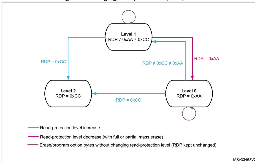
Table 20. Access status versus protection level and execution modes
| Area | Protection level | User execution (BootFromFlash) | Debug/ BootFromRam/ BootFromLoader | ||||
|---|---|---|---|---|---|---|---|
| Read | Write | Erase | Read | Write | Erase | ||
| Main flash memory | 1 | Yes | Yes | Yes | No | No | No (3) |
| 2 | Yes | Yes | Yes | N/A (1) | N/A (1) | N/A (1) | |
| System memory (2) | 1 | Yes | No | No | Yes | No | No |
| 2 | Yes | No | No | N/A (1) | N/A (1) | N/A (1) | |
| Option bytes | 1 | Yes | Yes (3) | Yes | Yes | Yes (3) | Yes |
| 2 | Yes | No | No | N/A (1) | N/A (1) | N/A (1) | |
| Backup registers | 1 | Yes | Yes | N/A (4) | No | No | N/A (4) |
| 2 | Yes | Yes | N/A | N/A (1) | N/A (1) | N/A (1) | |
| OTP | 1 | Yes | Yes | N/A | Yes | No | N/A |
| 2 | Yes | Yes | N/A | N/A (1) | N/A (1) | N/A (1) | |
- 1. When the protection Level 2 is active, the Debug port, the boot from RAM and the boot from system memory are disabled.
- 2. The system memory is only read-accessible, whatever the protection level (0, 1 or 2) and execution mode.
- 3. The main flash memory is erased when the RDP option byte is programmed with all level of protections disabled (0xAA).
- 4. The backup registers are cleared when RDP changes from Level 1 to Level 0.
3.5.2 FLASH proprietary code readout protection (PCROP)
Two areas of the flash memory (flash memory bank for dual-bank devices) can be protected against unwanted read and/or write by a third party.
The protected area is execute-only: it can only be reached by the STM32 CPU, with an instruction code, while all other accesses (DMA, debug and CPU data read, write and erase) are strictly prohibited. The PCROP areas have subpage (512-byte) granularity. An additional option bit (PCROP_RDP) allows to select if the PCROP area is erased or not when the RDP protection is changed from Level 1 to Level 0 (refer to Changing the read protection level ).
Each PCROP area is defined by a start subpage offset and an end subpage offset into the flash memory. These offsets are defined with the corresponding bitfields of the PCROP address registers FLASH PCROP area A start address register (FLASH_PCROP1ASR) , FLASH PCROP area A end address register (FLASH_PCROP1AER) , FLASH PCROP area B start address register (FLASH_PCROP1BSR) , and FLASH PCROP area B end address register (FLASH_PCROP1BER) for single-bank devices or for bank 1 of dual-bank devices, and in FLASH PCROP2 area A start address register (FLASH_PCROP2ASR) , FLASH PCROP2 area A end address register (FLASH_PCROP2AER) , FLASH PCROP2 area B start address register (FLASH_PCROP2BSR) , and FLASH PCROP2 area B end address register (FLASH_PCROP2BER) for bank 2 of dual-bank devices.
A PCROP area x (A or B) of flash memory bank y (1 or 2) is defined from the address:
Flash memory base address + [PCROP y x_STRT x 0x200] (included)
to the address:
Flash memory base address + [(PCROP y x_END + 1) x 0x200] (excluded).
The minimum PCROP area size is two PCROP subpages (2 x 512 bytes):
\( PCROP_{yx\_END} = PCROP_{yx\_STRT} + 1 \) .
When
\( PCROP_{yx\_END} = PCROP_{yx\_STRT} \) ,
the full flash memory (or bank y for dual-bank devices) is PCROP-protected.
For example, to PCROP-protect the address area from 0x0800 0800 to 0x0800 13FF, set the PCROP start subpage bitfield of the FLASH_PCROP1xSR register and the PCROP end subpage bitfield of the FLASH_PCROP1xER register ( x = A or B) as follows:
- – PCROP1x_STRT = 0x04 (PCROP area start address 0x0800 0800)
- – PCROP1x_END = 0x09 (PCROP area end address 0x0800 13FF)
Data read access to a PCROP-protected address raises the RDERR flag.
PCROP-protected addresses are also write protected. Write access to a PCROP-protected address raises the WRPERR flag.
PCROP-protected areas are also erase protected. Attempts to erase a page including at least one PCROP-protected subpage fails. Moreover, software mass erase cannot be performed if a PCROP-protected area is defined.
Deactivation of PCROP can only occur upon the RDP change from Level 1 to Level 0. Modification of user options to clear PCROP or to decrease the size of a PCROP-protected area do not have any effect to the PCROP areas. On the contrary, it is possible to increase the size of the PCROP-protected areas.
With the option bit PCROP_RDP cleared, the change of RDP from Level 1 to Level 0 triggers a partial mass erase that preserves the contents of the flash memory pages overlapping with PCROP-protected areas. Refer to section Changing the read protection level for details.
Table 21: PCROP protection
| PCROP register values (x = A or B, y = 1 or 2) | PCROP-protected area |
|---|---|
| PCROP y _START = PCROP y _END | Full flash memory |
| PCROP y _START > PCROP y _END (1) | None (unprotected) |
| PCROP y _START < PCROP y _END | Subpages from PCROP
y
_START to PCROP
y
_END (read-, write-, and erase-protected); PCROP area boundary pages (erase-protected). |
1. The PCROP y _START and PCROP y _END addresses must not point to the same flash memory page.
Note: With PCROP_RDP cleared, it is recommended to either define the PCROP area start and end onto flash memory page boundaries (2-Kbyte granularity), or to keep reserved and empty the PCROP-unprotected memory space of the PCROP area boundary pages (pages inside which the PCROP area starts and ends).
3.5.3 FLASH write protection (WRP)
The user area in flash memory can be protected against unwanted write operations. Two write-protected (WRP) areas can be defined, with page (2-Kbyte) granularity. Each area is defined by a start page offset and an end page offset related to the physical flash memory base address. These offsets are defined in the WRP address registers FLASH WRP area A address register (FLASH_WRP1AR) and FLASH WRP area B address register (FLASH_WRP1BR) , and, for dual-bank devices, also FLASH WRP2 area A address register (FLASH_WRP2AR) and FLASH WRP2 area B address register (FLASH_WRP2BR) .
The WRP x area ( x = A, B) of bank y ( y = 1 or 2) is defined from the address
Flash memory base address + [WRPy x _START x 0x0800] (included)
to the address
Flash memory base address + [(WRPy x _END+1) x 0x0800] (excluded).
The minimum WRP area size is one WRP page (2 Kbytes):
WRPy x _END = WRPy x _START .
For example, to protect the bank 1 of flash memory by WRP from the address 0x0800 1000 (included) to the address 0x0800 3FFF (included):
If boot in flash memory is selected, FLASH_WRP1AR register must be programmed with:
- – WRP1A_START = 0x02.
- – WRP1A_END = 0x07.
WRP1B_START and WRP1B_END in FLASH_WRP1BR can be used instead (area B in flash memory).
When WRP is active, it cannot be erased or programmed. Consequently, a software mass erase cannot be performed if one area is write-protected.
If an erase/program operation to a write-protected part of the flash memory is attempted, the write protection error flag (WRPERR) of the FLASH_SR register is set. This flag is also set for any write access to:
- – OTP area
- – part of the flash memory that can never be written like the ICP
- – PCROP area
Note: When the flash memory read protection level is selected (RDP level = 1), it is not possible to program or erase the memory if the CPU debug features are connected (single wire) or boot code is being executed from SRAM or system flash memory, even if WRP is not activated. Any attempt generates a hard fault (BusFault).
Table 22: WRP protection
| WRP registers values (x = A or B, y= 1 or 2) | WRP-protected area |
|---|---|
| WRPyx_STRT = WRPyx_END | Page WRPyx |
| WRPyx_STRT > WRPyx_END | None (unprotected) |
| WRPyx_STRT < WRPyx_END | Pages from WRPyx_STRT to WRPyx_END |
Note: To validate the WRP options, the option bytes must be reloaded by setting the OBL_LAUNCH bit in flash memory control register.
3.5.4 Securable memory area
The main purpose of the securable memory area is to protect a specific part of flash memory against undesired access. After system reset, the code in the securable memory area can only be executed until the securable area becomes secured and never again until the next system reset. This allows implementing software security services such as secure key storage or safe boot.
Securable memory area is located in the main flash memory. It is dedicated to executing trusted code. When not secured, the securable memory behaves like the rest of main flash memory. When secured (the SEC_PROT and SEC_PROT2 bits of the FLASH_CR register set, the latter pertaining to bank 2 in dual-bank devices), any access to securable memory area (fetch, read, programming, erase) is rejected, generating a bus error. The securable area can only be unsecured by a system reset.
The size of the securable memory area is defined by the SEC_SIZE[7:0] and SEC_SIZE2[7:0] (the latter for dual-bank devices only) bitfields of the FLASH_SECR register. For STM32G071xx and STM32G081xx, it can only be modified in RDP level 0. For all the other devices, it can only be modified in RDP level 0 or 1, with SEC_PROT = 0 and SEC_PROT2 = 0 specifically on STM32G0B1xx and STM32G0C1xx. Its content is erased upon changing from RDP Level 1 to Level 0, even if it overlaps with PCROP subpages.
Note: The securable memory area start address is 0x0800 0000. Before activating the securable memory area, move the vector table outside the page 0 if necessary.
Note: Upon change from RDP Level 1 to Level 0 while the PCROP_RDP bit is cleared, the securable memory area is erased even if it overlaps with the PCROP subpages. The PCROP subpages not overlapping with the securable memory area are not erased. See Table 23.
Table 23. Securable memory erase at RDP Level 1 to Level 0 change
| Securable memory size (SEC_SIZE x [7:0]) | PCROP_RDP | Erased pages |
|---|---|---|
| 0 | 1 | All (mass erase) |
| 0 | 0 | All but PCROP |
| > 0 | 1 | All (mass erase) |
| > 0 | 0 | All but PCROP outside the securable memory area |
3.5.5 Disabling core debug access
For executing sensitive code or manipulating sensitive data in securable memory area, the debug access to the core can temporarily be disabled.
Figure 4 gives an example of managing DBG_SWEN and SEC_PROT (or SEC_PROT2, for bank 2 in dual-bank devices) bits.
Figure 4. Example of disabling core debug access
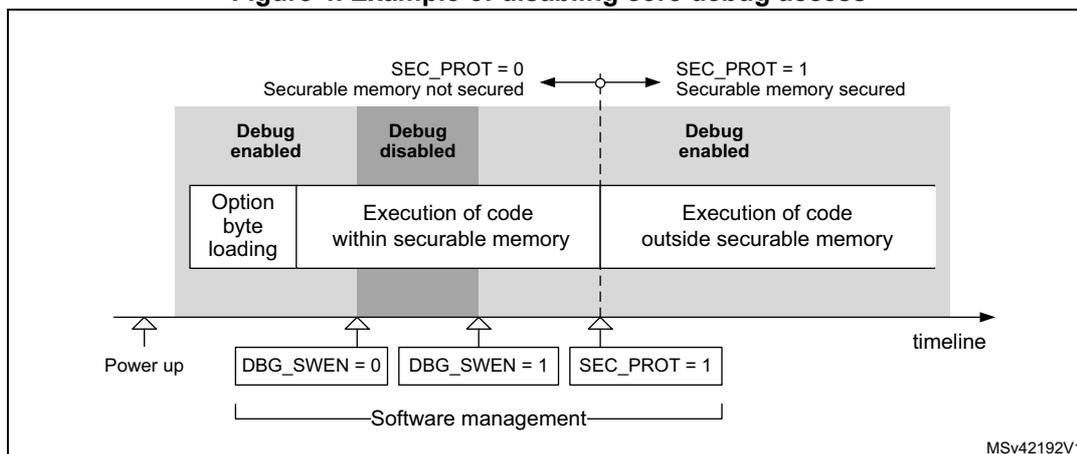
The diagram illustrates the timeline for disabling core debug access. It is divided into three main phases based on the state of the SEC_PROT bit:
- SEC_PROT = 0 (Securable memory not secured):
This phase is further divided into:
- Debug enabled: Corresponds to the 'Option byte loading' and 'Execution of code within securable memory' stages.
- Debug disabled: A brief transition state.
- SEC_PROT = 1 (Securable memory secured): This phase corresponds to the 'Execution of code outside securable memory' stage, where 'Debug enabled' is shown.
- Power up
- DBG_SWEN = 0
- DBG_SWEN = 1
- SEC_PROT = 1
3.5.6 Forcing boot from main flash memory
To increase the security and establish a chain of trust, the BOOT_LOCK option bit of the FLASH_SECR register allows forcing the system to boot from the main flash memory regardless the other boot mode configuration bits or the empty check flag. It is always possible to set the BOOT_LOCK bit. However, it is possible to reset it only when:
- • RDP is set to Level 0, or
- • RDP is set to Level 1, while Level 0 is requested and a full mass-erase is performed.
Caution: If BOOT_LOCK is set in association with RDP level 1, the debug capabilities of the device are stopped and the reset value of the DBG_SWEN bit of the FLASH access control register (FLASH_ACR) becomes zero. If DBG_SWEN bit is not set by the application code after reset, there is no way to recover from this situation.
3.6 FLASH interrupts
Table 24. FLASH interrupt requests
| Interrupt event | Event flag | Event flag/interrupt clearing method | Interrupt enable control bit |
|---|---|---|---|
| End of operation | EOP (1) | Write EOP=1 | EOPPIE |
| Operation error | OPERR (2) | Write OPERR=1 | ERRIE |
| Read protection error | RDERR | Write RDERR=1 | RDERRIE |
| Write protection error | WRPERR | Write WRPERR=1 | N/A |
| Size error | SIZERR | Write SIZERR=1 | N/A |
| Programming sequential error | PROGERR | Write PROGERR=1 | N/A |
| Programming alignment error | PGAERR | Write PGAERR=1 | N/A |
| Programming sequence error | PGSERR | Write PGSERR=1 | N/A |
| Data miss during fast programming error | MISSERR | Write MISSERR=1 | N/A |
| Fast programming error | FASTERR | Write FASTERR=1 | N/A |
| ECC error correction | ECCC | Write ECCC=1 | ECCIE |
| ECC double error (NMI) | ECCD | Write ECCD=1 | N/A |
1. EOP is set only if EOPPIE is set.
2. OPERR is set only if ERRIE is set.
3.7 FLASH registers
3.7.1 FLASH access control register (FLASH_ACR)
Address offset: 0x000
Reset value: 0b0000 0000 0000 010X 0000 0110 0000 0000 (EMPTY bit is updated only by OBL, it is not affected by a system reset)
| 31 | 30 | 29 | 28 | 27 | 26 | 25 | 24 | 23 | 22 | 21 | 20 | 19 | 18 | 17 | 16 |
|---|---|---|---|---|---|---|---|---|---|---|---|---|---|---|---|
| Res. | Res. | Res. | Res. | Res. | Res. | Res. | Res. | Res. | Res. | Res. | Res. | Res. | DBG_SWEN | Res. | EMPTY |
| rw | rw | ||||||||||||||
| 15 | 14 | 13 | 12 | 11 | 10 | 9 | 8 | 7 | 6 | 5 | 4 | 3 | 2 | 1 | 0 |
| Res. | Res. | Res. | Res. | ICRST | Res. | ICEN | PRFTEN | Res. | Res. | Res. | Res. | Res. | LATENCY[2:0] | ||
| rw | rw | rw | rw | rw | rw |
Bits 31:19 Reserved, must be kept at reset value.
Bit 18 DBG_SWEN : Debug access software enable
Software may use this bit to enable/disable the debugger read access.
0: Debugger disabled
1: Debugger enabled
Bit 17 Reserved, must be kept at reset value.
Bit 16 EMPTY : Main flash memory area empty
This bit indicates whether the first location of the main flash memory area was read as erased or as programmed during OBL. It is not affected by a system reset.
Software may need to change this bit value after a flash memory program or erase operation.
0: Main flash memory area programmed
1: Main flash memory area empty
The bit can be set and reset by software.
Bits 15:12 Reserved, must be kept at reset value.
Bit 11 ICRST : CPU Instruction cache reset
0: CPU Instruction cache is not reset
1: CPU Instruction cache is reset
This bit can be written only when the instruction cache is disabled.
Bit 10 Reserved, must be kept at reset value.
Bit 9 ICEN : CPU Instruction cache enable
0: CPU Instruction cache is disabled
1: CPU Instruction cache is enabled
Bit 8 PRFTEN : CPU Prefetch enable
0: CPU Prefetch disabled
1: CPU Prefetch enabled
Bits 7:3 Reserved, must be kept at reset value.
Bits 2:0 LATENCY[2:0] : Flash memory access latency
The value in this bitfield configures the number of CPU wait states inserted when accessing the flash memory.
000: Zero wait states
001: One wait state
010: Two wait states
Others: Reserved
A new write into the bitfield becomes effective when it returns the same value upon read.
3.7.2 FLASH key register (FLASH_KEYR)
Address offset: 0x008
Reset value: 0x0000 0000

| 31 | 30 | 29 | 28 | 27 | 26 | 25 | 24 | 23 | 22 | 21 | 20 | 19 | 18 | 17 | 16 |
| KEY[31:16] | |||||||||||||||
| w | w | w | w | w | w | w | w | w | w | w | w | w | w | w | w |
| 15 | 14 | 13 | 12 | 11 | 10 | 9 | 8 | 7 | 6 | 5 | 4 | 3 | 2 | 1 | 0 |
| KEY[15:0] | |||||||||||||||
| w | w | w | w | w | w | w | w | w | w | w | w | w | w | w | w |
Bits 31:0 KEY[31:0] : FLASH key
The following values must be written consecutively to unlock the FLASH control register (FLASH_CR) , thus enabling programming/erasing operations:
KEY1: 0x4567 0123
KEY2: 0xCDEF 89AB
3.7.3 FLASH option key register (FLASH_OPTKEYR)
Address offset: 0x00C
Reset value: 0x0000 0000

| 31 | 30 | 29 | 28 | 27 | 26 | 25 | 24 | 23 | 22 | 21 | 20 | 19 | 18 | 17 | 16 |
| OPTKEY[31:16] | |||||||||||||||
| w | w | w | w | w | w | w | w | w | w | w | w | w | w | w | w |
| 15 | 14 | 13 | 12 | 11 | 10 | 9 | 8 | 7 | 6 | 5 | 4 | 3 | 2 | 1 | 0 |
| OPTKEY[15:0] | |||||||||||||||
| w | w | w | w | w | w | w | w | w | w | w | w | w | w | w | w |
Bits 31:0 OPTKEY[31:0] : Option byte key
The following values must be written consecutively to unlock the flash memory option registers, enabling option byte programming/erasing operations:
KEY1: 0x0819 2A3B
KEY2: 0x4C5D 6E7F
3.7.4 FLASH status register (FLASH_SR)
Address offset: 0x010
Reset value: 0x000X 0000
| 31 | 30 | 29 | 28 | 27 | 26 | 25 | 24 | 23 | 22 | 21 | 20 | 19 | 18 | 17 | 16 |
|---|---|---|---|---|---|---|---|---|---|---|---|---|---|---|---|
| Res. | Res. | Res. | Res. | Res. | Res. | Res. | Res. | Res. | Res. | Res. | Res. | Res. | CFGBSY | BSY2 | BSY1 |
| r | r | r | |||||||||||||
| 15 | 14 | 13 | 12 | 11 | 10 | 9 | 8 | 7 | 6 | 5 | 4 | 3 | 2 | 1 | 0 |
| OPTV ERR | RD ERR | Res. | Res. | Res. | Res. | FAST ERR | MISS ERR | PGS ERR | SIZ ERR | PGA ERR | WRP ERR | PROG ERR | Res. | OP ERR | EOP |
| rc_w1 | rc_w1 | rc_w1 | rc_w1 | rc_w1 | rc_w1 | rc_w1 | rc_w1 | rc_w1 | rc_w1 | rc_w1 |
Bits 31:19 Reserved, must be kept at reset value.
Bit 18 CFGBSY : Programming or erase configuration busy.
The flag is set and reset by hardware.
The flag high level indicates that a program or erase operation is ongoing, based on the current FLASH control register (FLASH_CR) settings. As long as the flag remains high, the FLASH_CR register must not be written (this causes HardFault) and the software cannot start another flash memory operation.
For flash memory program operation , the flag is set when the first word is sent. It is cleared after the second word is sent, when the operation completes or ends with an error.
For flash memory erase operation , the flag is set when setting STRT bit of FLASH control register (FLASH_CR) . It is cleared when the operation completes or ends with an error.
Note: The flag is also set with the first byte of an access to the locked flash memory. In this case, a complete double word sent to the flash memory must be finished in order to clear the flag.
Bit 17 BSY2 : Bank 2 busy
This flag indicates that a flash memory bank 2 operation requested by FLASH control register (FLASH_CR) is in progress. This bit is set at the beginning of the flash memory operation, and cleared when the operation finishes or when an error occurs.
Bit 16 BSY1 : Bank 1 busy
This flag indicates that a flash memory (bank 1 for dual-bank devices) operation requested by FLASH control register (FLASH_CR) is in progress. This bit is set at the beginning of the flash memory operation, and cleared when the operation finishes or when an error occurs.
Bit 15 OPTVERR : Option and Engineering bits loading validity error
Set by hardware when the options and engineering bits read may not be the one configured by the user or production. If options and engineering bits haven't been properly loaded, OPTVERR is set again after each system reset. Option bytes that fail loading are forced to a safe value, see Section 3.4.2: FLASH option byte programming .
Cleared by writing 1.
Bit 14 RDERR : PCROP read error
Set by hardware when an address to be read belongs to a read protected area of the flash memory (PCROP protection). An interrupt is generated if RDERRIE is set in FLASH_CR. Cleared by writing 1.
Bits 13:10 Reserved, must be kept at reset value.
Bit 9 FASTERR: Fast programming errorSet by hardware when a fast programming sequence (activated by FSTPG) is interrupted due to an error (alignment, size, write protection or data miss). The corresponding status bit (PGAERR, SIZERR, WRPERR or MISSERR) is set at the same time.
Cleared by writing 1.
Bit 8 MISSERR: Fast programming data miss errorIn Fast programming mode, 32 double words (256 bytes) must be sent to flash memory successively, and the new data must be sent to the logic control before the current data is fully programmed. MISSERR is set by hardware when the new data is not present in time.
Cleared by writing 1.
Bit 7 PGSERR: Programming sequence errorSet by hardware when a write access to the flash memory is performed by the code while PG or FSTPG have not been set previously. Set also by hardware when PROGERR, SIZERR, PGAERR, WRPERR, MISSERR or FASTERR is set due to a previous programming error.
Cleared by writing 1.
Bit 6 SIZERR: Size errorSet by hardware when the size of the access is a byte or half-word during a program or a fast program sequence. Only double word programming is allowed (consequently: word access).
Cleared by writing 1.
Bit 5 PGAERR: Programming alignment errorSet by hardware when the data to program cannot be contained in the same double word (64-bit) flash memory in case of standard programming, or if there is a change of page during fast programming.
Cleared by writing 1.
Bit 4 WRPERR: Write protection errorSet by hardware when an address to be erased/programmed belongs to a write-protected part (by WRP, PCROP or RDP Level 1) of the flash memory.
Cleared by writing 1.
Bit 3 PROGERR: Programming errorSet by hardware when a double-word address to be programmed contains a value different from '0xFFFF FFFF' before programming, except if the data to write is '0x0000 0000'.
Cleared by writing 1.
Bit 2 Reserved, must be kept at reset value. Bit 1 OPERR: Operation errorSet by hardware when a flash memory operation (program / erase) completes unsuccessfully.
This bit is set only if error interrupts are enabled (ERRIE=1).
Cleared by writing '1'.
Bit 0 EOP: End of operationSet by hardware when one or more flash memory operation (programming / erase) has been completed successfully.
This bit is set only if the end of operation interrupts are enabled (EOPIE=1).
Cleared by writing 1.
3.7.5 FLASH control register (FLASH_CR)
Address offset: 0x014
Reset value: 0xC000 0000
Access: no wait state when no flash memory operation is on going, word, half-word and byte access
Do not write this register as long as CFGBSY in FLASH status register (FLASH_SR) is high, as such a write causes a HardFault exception.
| 31 | 30 | 29 | 28 | 27 | 26 | 25 | 24 | 23 | 22 | 21 | 20 | 19 | 18 | 17 | 16 |
|---|---|---|---|---|---|---|---|---|---|---|---|---|---|---|---|
| LOCK | OPT LOCK | SEC PROT2 | SEC PROT | OBL LAUNCH | RD ERRIE | ERRIE | EOPIE | Res. | Res. | Res. | Res. | Res. | FSTPG | OPT STRT | STRT |
| rs | rs | rw | rw | rc_w1 | rw | rw | rw | rw | rs | rs | |||||
| 15 | 14 | 13 | 12 | 11 | 10 | 9 | 8 | 7 | 6 | 5 | 4 | 3 | 2 | 1 | 0 |
| MER2 | Res. | BKER | Res. | Res. | Res. | PNB[6:0] | MER1 | PER | PG | ||||||
| rw | rw | rw | rw | rw | rw | rw | rw | rw | rw | rw | rw | ||||
Bit 31 LOCK: FLASH_CR lock
This bit is set only. When set, the FLASH_CR register is locked. It is cleared by hardware after detecting the unlock sequence.
In case of an unsuccessful unlock operation, this bit remains set until the next system reset.
Bit 30 OPTLOCK: Options lock
This bit is set only. When set, all bits concerning user option in FLASH_CR register and so option page are locked. Furthermore, it is not possible to write the option registers. This bit is cleared by hardware after detecting the unlock sequence. The LOCK bit must be cleared before doing the unlock sequence for OPTLOCK bit.
In case of an unsuccessful unlock operation, this bit remains set until the next reset.
Bit 29 SEC_PROT2: Securable memory area protection enable, bank 2
This bit enables the protection on securable area in bank 2, provided that a non-null securable memory area size (SEC_SIZE2[7:0]) is defined in option bytes.
0: Disable (securable area accessible)
1: Enable (securable area not accessible)
This bit is possible to set only by software and to clear only through a system reset.
Bit 28 SEC_PROT: Securable memory area protection enable (bank 1)
This bit enables the protection on securable area (in bank 1 for dual-bank devices), provided that a non-null securable memory area size (SEC_SIZE[7:0]) is defined in option bytes.
0: Disable (securable area accessible)
1: Enable (securable area not accessible)
This bit is possible to set only by software and to clear only through a system reset.
Bit 27 OBL_LAUNCH: Option byte load launch
When set, this bit triggers the load of option bytes into option registers. It is automatically cleared upon the completion of the load. The high state of the bit indicates pending option byte load.
The bit cannot be cleared by software. It cannot be written as long as OPTLOCK is set.
Bit 26 RDERRIE: PCROP read error interrupt enable
This bit enables the interrupt generation upon setting the RDERR flag in the FLASH_SR register.
0: Disable
1: Enable
Bit 25 ERRIE : Error interrupt enable
This bit enables the interrupt generation upon setting the OPERR flag in the FLASH_SR register.
0: Disable
1: Enable
Bit 24 EOPIE : End-of-operation interrupt enable
This bit enables the interrupt generation upon setting the EOP flag in the FLASH_SR register.
0: Disable
1: Enable
Bits 23:19 Reserved, must be kept at reset value.
Bit 18 FSTPG : Fast programming enable
0: Disable
1: Enable
Bit 17 OPTSTR : Start of modification of option bytes
Setting this bit triggers the modification of option bytes.
This bit is set only by software, and is cleared when the BSY1 bit is cleared in FLASH_SR. It cannot be set as long as OPTLOCK is high.
Bit 16 STRT : Start erase operation
This bit triggers an erase operation when set.
This bit is possible to set only by software and to clear only by hardware. The hardware clears it when one of BSY1 and BSY2 flags in the FLASH_SR register transits to zero.
Bit 15 MER2 : Mass erase, bank 2
When set, this bit triggers the mass erase of bank 2 (all user pages).
Bit 14 Reserved, must be kept at reset value.
Bit 13 BKER : Bank selection for erase operation
This bit selects the target of erase operation (bank 1 or bank 2).
0: Bank 1
1: Bank 2
The bit has no effect on the single-bank devices.
Bits 12:10 Reserved, must be kept at reset value.
Bits 9:3 PNB[6:0] : Page number selection
These bits select the page to erase:
0x00: page 0
0x01: page 1
...
0x7F: page 127
Note: Values corresponding to addresses outside the main memory are not allowed.
Bit 2 MER1 : Mass erase (bank 1)
When set, this bit triggers the mass erase, that is, all user pages (of bank 1 for dual-bank devices).
Bit 1 PER : Page erase enable
0: Disable
1: Enable
Bit 0 PG : Flash memory programming enable
0: Disable
1: Enable
3.7.6 FLASH ECC register (FLASH_ECCR)
Address offset: 0x018
Reset value: 0x0000 0000
Access: no wait state when no flash memory operation is on going, word, half-word and byte access
This register applies to single-bank devices and to bank 1 of dual-bank devices.
| 31 | 30 | 29 | 28 | 27 | 26 | 25 | 24 | 23 | 22 | 21 | 20 | 19 | 18 | 17 | 16 |
|---|---|---|---|---|---|---|---|---|---|---|---|---|---|---|---|
| ECCD | ECCC | Res. | Res. | Res. | Res. | Res. | ECCIE | Res. | Res. | Res. | SYSF_ECC | Res. | Res. | Res. | Res. |
| rc_w1 | rc_w1 | rw | r | ||||||||||||
| 15 | 14 | 13 | 12 | 11 | 10 | 9 | 8 | 7 | 6 | 5 | 4 | 3 | 2 | 1 | 0 |
| ADDR_ECC[15:0] | |||||||||||||||
| r | r | r | r | r | r | r | r | r | r | r | r | r | r | r | r |
Bit 31 ECCD: ECC detection
Set by hardware when two ECC errors have been detected. When this bit is set, a NMI is generated.
Cleared by writing 1.
Bit 30 ECCC: ECC correction
Set by hardware when one ECC error has been detected and corrected. An interrupt is generated if ECCIE is set.
Cleared by writing 1.
Bits 29:25 Reserved, must be kept at reset value.
Bit 24 ECCIE: ECC correction interrupt enable
0: ECCC interrupt disabled
1: ECCC interrupt enabled
Bits 23:21 Reserved, must be kept at reset value.
Bit 20 SYSF_ECC: System flash memory ECC fail
This bit indicates that the ECC error correction or double ECC error detection is located in the system flash memory.
Bits 19:16 Reserved, must be kept at reset value.
Bits 15:0 ADDR_ECC[15:0]: ECC fail double-word address offset
In case of ECC error or ECC correction detected, this bitfield contains double-word offset (multiple of 64 bits) to main flash memory.
3.7.7 FLASH ECC register 2 (FLASH_ECCR2)
Address offset: 0x01C
Reset value: 0x0000 0000
Access: no wait state when no flash memory operation is on going, word, half-word and byte access
This register applies to bank 2 of dual-bank devices.
| 31 | 30 | 29 | 28 | 27 | 26 | 25 | 24 | 23 | 22 | 21 | 20 | 19 | 18 | 17 | 16 |
|---|---|---|---|---|---|---|---|---|---|---|---|---|---|---|---|
| ECCD | ECCC | Res. | Res. | Res. | Res. | Res. | ECCCIE | Res. | Res. | Res. | SYSF_ECC | Res. | Res. | Res. | Res. |
| rc_w1 | rc_w1 | rw | r | ||||||||||||
| 15 | 14 | 13 | 12 | 11 | 10 | 9 | 8 | 7 | 6 | 5 | 4 | 3 | 2 | 1 | 0 |
| ADDR_ECC[15:0] | |||||||||||||||
| r | r | r | r | r | r | r | r | r | r | r | r | r | r | r | r |
Bit 31 ECCD: ECC detection
Set by hardware when two ECC errors have been detected. When this bit is set, a NMI is generated.
Cleared by writing 1.
Bit 30 ECCC: ECC correction
Set by hardware when one ECC error has been detected and corrected. An interrupt is generated if ECCIE is set.
Cleared by writing 1.
Bits 29:25 Reserved, must be kept at reset value.
Bit 24 ECCCIE: ECC correction interrupt enable
0: ECCC interrupt disabled
1: ECCC interrupt enabled
Bits 23:21 Reserved, must be kept at reset value.
Bit 20 SYSF_ECC: System flash memory ECC fail
This bit indicates that the ECC error correction or double ECC error detection is located in the system flash memory.
Bits 19:16 Reserved, must be kept at reset value.
Bits 15:0 ADDR_ECC[15:0]: ECC fail double-word address offset
In case of ECC error or ECC correction detected, this bitfield contains double-word offset (multiple of 64 bits) to main flash memory.
3.7.8 FLASH option register (FLASH_OPTR)
Address offset: 0x020
Reset value: 0b11XX XXXX 1XXX XXXX XXXX XXXX XXXX XXXX
The option bits are loaded with values from flash memory at power-on reset release.
Access: no wait state when no flash memory operation is on going, word, half-word and byte access
| 31 | 30 | 29 | 28 | 27 | 26 | 25 | 24 | 23 | 22 | 21 | 20 | 19 | 18 | 17 | 16 |
|---|---|---|---|---|---|---|---|---|---|---|---|---|---|---|---|
| Res. | Res. | IRHEN | NRST_MODE [1:0] | nBOOT0 | nBOOT1 | nBOOT_SEL | Res. | RAM PARITY CHECK | DUAL BANK | nSWAP _BANK | WWDG _SW | IWDG _STDBY | IWDG _STOP | IWDG _SW | |
| rw | rw | rw | rw | rw | rw | rw | rw | rw | rw | rw | rw | rw | |||
| 15 | 14 | 13 | 12 | 11 | 10 | 9 | 8 | 7 | 6 | 5 | 4 | 3 | 2 | 1 | 0 |
| nRST SHDW | nRST STDBY | nRST STOP | BORF_LEV[1:0] | BORR_LEV[1:0] | BOR _EN | RDP[7:0] | |||||||||
| rw | rw | rw | rw | rw | rw | rw | rw | rw | rw | rw | rw | rw | rw | rw | rw |
Bits 31:30 Reserved, must be kept at reset value.
Bit 29 IRHEN : Internal reset holder enable bit
0: Internal resets are propagated as simple pulse on the reset pin
1: Internal resets drives the reset pin low until it is seen as low level
Bits 28:27 NRST_MODE[1:0] : PF2-NRST mode
00: Reserved
01: Reset Input only: a low level on the PF2-NRST pin generates system reset, internal resets not propagated to the PF2-NRST pin
10: GPIO: GPIO pad functionality, only internal resets possible
11: Bidirectional reset: PF2-NRST pin configured in reset input/output mode (legacy mode)
Note: For GPIO mode, refer to Section 7.3.17: Reset pin (PF2-NRST) in GPIO mode for additional considerations.
Bit 26 nBOOT0 : nBOOT0 option bit
0: nBOOT0=0
1: nBOOT0=1
Bit 25 nBOOT1 : Boot configuration
Together with the BOOT0 pin or option bit nBOOT0 (depending on nBOOT_SEL option bit configuration), this bit selects boot mode from the main flash memory, SRAM or the system memory. Refer to Section 2.5: Boot configuration
Bit 24 nBOOT_SEL
0: BOOT0 signal is defined by BOOT0 pin value (legacy mode)
1: BOOT0 signal is defined by nBOOT0 option bit
Bit 23 Reserved, must be kept at reset value.
Bit 22 RAM_PARITY_CHECK : SRAM parity check control
0: SRAM parity check enable
1: SRAM parity check disable
Bit 21 DUAL_BANK : Flash memory bank configuration for 256 Kbyte devices
This bit is only available on STM32G0B1xx and STM32G0C1xx and only effective for 256-Kbyte devices. Regardless of this bit, the 512-Kbyte devices always operate in dual-bank mode and the 128-Kbyte devices in single-bank mode. Refer to Table 10 and Table 11 .
0: Single-bank flash memory
1: Dual-bank flash memory
Note: This bit has no effect on the erase and write protection (WRP) operations.
Bit 20 nSWAP_BANK : Flash memory bank access swap control
This bit controls the flash memory bank swap. With no swap, the flash memory bank accessed through the address range starting at 0x0800 0000 is the physical bank 1. With swap, it is the bank 2.
0: Swap (bank 2 mapped from 0x0800 0000)
1: No swap (bank 1 mapped from 0x0800 0000)
This bit pertains to dual-bank devices only. In single-bank devices, it is reserved.
Note: This bit has no effect on the erase and write protection (WRP) operations.
Bit 19 WWDG_SW : Window watchdog selection
0: Hardware window watchdog
1: Software window watchdog
Bit 18 IWDG_STDBY : Independent watchdog counter freeze in Standby mode
0: Independent watchdog counter is frozen in Standby mode
1: Independent watchdog counter is running in Standby mode
Bit 17 IWDG_STOP : Independent watchdog counter freeze in Stop mode
0: Independent watchdog counter is frozen in Stop mode
1: Independent watchdog counter is running in Stop mode
Bit 16 IWDG_SW : Independent watchdog selection
0: Hardware independent watchdog
1: Software independent watchdog
Bit 15 nRST_SHDW
0: Reset generated when entering the Shutdown mode
1: No reset generated when entering the Shutdown mode
Bit 14 nRST_STDBY
0: Reset generated when entering the Standby mode
1: No reset generated when entering the Standby mode
Bit 13 nRST_STOP
0: Reset generated when entering the Stop mode
1: No reset generated when entering the Stop mode
Bits 12:11 BORF_LEV[1:0] : BOR threshold at falling \( V_{DD} \) supply
Falling \( V_{DD} \) crossings this threshold activates the reset signal.
00: BOR falling level 1 with threshold around 2.0 V
01: BOR falling level 2 with threshold around 2.2 V
10: BOR falling level 3 with threshold around 2.5 V
11: BOR falling level 4 with threshold around 2.8 V
Bits 10:9 BORR_LEV[1:0] : BOR threshold at rising \( V_{DD} \) supply
Rising \( V_{DD} \) crossings this threshold releases the reset signal.
00: BOR rising level 1 with threshold around 2.1 V
01: BOR rising level 2 with threshold around 2.3 V
10: BOR rising level 3 with threshold around 2.6 V
11: BOR rising level 4 with threshold around 2.9 V
Bit 8 BOR_EN : Brown out reset enable
0: Configurable brown out reset disabled, power-on reset defined by POR/PDR levels
1: Configurable brown out reset enabled, values of BORR_LEV_RISING and
BORF_LEV_FALLING taken into account
Bits 7:0 RDP[7:0] : Read protection level
Note: 0xAA: Level 0, read protection not active
0xCC: Level 2, chip read protection active
Others: Level 1, memories read protection active
3.7.9 FLASH PCROP area A start address register (FLASH_PCROP1ASR)
Address offset: 0x024
Reset value: 0b0000 0000 0000 0000 0000 000X XXXX XXXX (The option bits are loaded with values from flash memory at power-on reset release.)
Access: no wait state when no flash memory operation is on going, word, half-word access
This register applies to single-bank devices and to bank 1 of dual-bank devices.
| 31 | 30 | 29 | 28 | 27 | 26 | 25 | 24 | 23 | 22 | 21 | 20 | 19 | 18 | 17 | 16 |
|---|---|---|---|---|---|---|---|---|---|---|---|---|---|---|---|
| Res. | Res. | Res. | Res. | Res. | Res. | Res. | Res. | Res. | Res. | Res. | Res. | Res. | Res. | Res. | Res. |
| 15 | 14 | 13 | 12 | 11 | 10 | 9 | 8 | 7 | 6 | 5 | 4 | 3 | 2 | 1 | 0 |
| Res. | Res. | Res. | Res. | Res. | Res. | Res. | PCROP1A_STR[8:0] | ||||||||
| rw | rw | rw | rw | rw | rw | rw | rw | rw | |||||||
Bits 31:9 Reserved, must be kept at reset value.
Bits 8:0 PCROP1A_STR[8:0] : PCROP1A area start offset (bank 1)
Contains the offset of the first subpage of the PCROP1A area (in bank 1 for dual-bank devices).
Note: The number of effective bits depends on the size of flash memory in the device.
3.7.10 FLASH PCROP area A end address register (FLASH_PCROP1AER)
Address offset: 0x028
Reset value: 0bX000 0000 0000 0000 0000 000X XXXX XXXX (The option bits are loaded with values from flash memory at power-on reset release.)
Access: no wait state when no flash memory operation is on going, word, half-word access. PCROP_RDP bit can be accessed with byte access
| 31 | 30 | 29 | 28 | 27 | 26 | 25 | 24 | 23 | 22 | 21 | 20 | 19 | 18 | 17 | 16 |
|---|---|---|---|---|---|---|---|---|---|---|---|---|---|---|---|
| PCROP_RDP | Res. | Res. | Res. | Res. | Res. | Res. | Res. | Res. | Res. | Res. | Res. | Res. | Res. | Res. | Res. |
| rs | |||||||||||||||
| 15 | 14 | 13 | 12 | 11 | 10 | 9 | 8 | 7 | 6 | 5 | 4 | 3 | 2 | 1 | 0 |
| Res. | Res. | Res. | Res. | Res. | Res. | Res. | PCROP1A_END[8:0] | ||||||||
| rw | rw | rw | rw | rw | rw | rw | rw | rw | |||||||
Bit 31 PCROP_RDP : PCROP area erase upon RDP level regression
This bit determines whether the PCROP area (and the totality of the PCROP area boundary pages) is erased by the mass erase triggered by the RDP level regression from Level 1 to Level 0:
0: Not erased
1: Erased
The software can only set this bit. It is automatically reset upon mass erase following the RDP regression from Level 1 to Level 0.
Bits 30:9 Reserved, must be kept at reset value.
Bits 8:0 PCROP1A_END[8:0] : PCROP1A area end offset (bank 1)
Contains the offset of the last subpage of the PCROP1A area (in bank 1 for dual-bank devices).
Note: The number of effective bits depends on the size of flash memory in the device.
3.7.11 FLASH WRP area A address register (FLASH_WRP1AR)
Address offset: 0x02C
Reset value: 0x00XX 00XX (The option bits are loaded with values from flash memory at power-on reset release.)
Access: no wait state when no flash memory operation is on going, word, half-word and byte access.
| 31 | 30 | 29 | 28 | 27 | 26 | 25 | 24 | 23 | 22 | 21 | 20 | 19 | 18 | 17 | 16 |
|---|---|---|---|---|---|---|---|---|---|---|---|---|---|---|---|
| Res. | Res. | Res. | Res. | Res. | Res. | Res. | Res. | Res. | WRP1A_END[6:0] | ||||||
| rw | rw | rw | rw | rw | rw | rw | |||||||||
| 15 | 14 | 13 | 12 | 11 | 10 | 9 | 8 | 7 | 6 | 5 | 4 | 3 | 2 | 1 | 0 |
| Res. | Res. | Res. | Res. | Res. | Res. | Res. | Res. | Res. | WRP1A_STRT[6:0] | ||||||
| rw | rw | rw | rw | rw | rw | rw | |||||||||
Bits 31:23 Reserved, must be kept at reset value.
Bits 22:16 WRP1A_END[6:0] : WRP area A end offset (bank 1)
This bitfield contains the offset of the last page of the WRP area A (in bank 1 for dual-bank devices).
Note: The number of effective bits depends on the size of flash memory in the device.
Bits 15:7 Reserved, must be kept at reset value.
Bits 6:0 WRP1A_STRT[6:0] : WRP area A start offset (bank 1)
This bitfield contains the offset of the first page of the WRP area A (in bank 1 for dual-bank devices).
Note: The number of effective bits depends on the size of flash memory in the device.
3.7.12 FLASH WRP area B address register (FLASH_WRP1BR)
Address offset: 0x030
Reset value: 0b0000 0000 0XXX XXXX 0000 0000 0XXX XXXX (The option bits are loaded with values from flash memory at power-on reset release.)
Access: no wait state when no flash memory operation is on going, word, half-word and byte access.
| 31 | 30 | 29 | 28 | 27 | 26 | 25 | 24 | 23 | 22 | 21 | 20 | 19 | 18 | 17 | 16 |
|---|---|---|---|---|---|---|---|---|---|---|---|---|---|---|---|
| Res. | Res. | Res. | Res. | Res. | Res. | Res. | Res. | Res. | WRP1B_END[6:0] | ||||||
| rw | rw | rw | rw | rw | rw | rw | |||||||||
| 15 | 14 | 13 | 12 | 11 | 10 | 9 | 8 | 7 | 6 | 5 | 4 | 3 | 2 | 1 | 0 |
|---|---|---|---|---|---|---|---|---|---|---|---|---|---|---|---|
| Res. | Res. | Res. | Res. | Res. | Res. | Res. | Res. | Res. | WRP1B_STRT[6:0] | ||||||
| rw | rw | rw | rw | rw | rw | rw | |||||||||
Bits 31:23 Reserved, must be kept at reset value.
Bits 22:16 WRP1B_END[6:0] : WRP area B end offset (bank 1)
This bitfield contains the offset of the last page of the WRP area B (in bank 1 for dual-bank devices).
Note: The number of effective bits depends on the size of flash memory in the device.
Bits 15:7 Reserved, must be kept at reset value.
Bits 6:0 WRP1B_STRT[6:0] : WRP area B start offset (bank 1)
This bitfield contains the offset of the first page of the WRP area B (in bank 1 for dual-bank devices).
Note: The number of effective bits depends on the size of flash memory in the device.
3.7.13 FLASH PCROP area B start address register (FLASH_PCROP1BSR)
Address offset: 0x034
Reset value: 0b0000 0000 0000 0000 0000 000X XXXX XXXX (The option bits are loaded with values from flash memory at power-on reset release.)
Access: no wait state when no flash memory operation is on going, word, half-word access
| 31 | 30 | 29 | 28 | 27 | 26 | 25 | 24 | 23 | 22 | 21 | 20 | 19 | 18 | 17 | 16 |
|---|---|---|---|---|---|---|---|---|---|---|---|---|---|---|---|
| Res. | Res. | Res. | Res. | Res. | Res. | Res. | Res. | Res. | Res. | Res. | Res. | Res. | Res. | Res. | Res. |
| 15 | 14 | 13 | 12 | 11 | 10 | 9 | 8 | 7 | 6 | 5 | 4 | 3 | 2 | 1 | 0 |
| Res. | Res. | Res. | Res. | Res. | Res. | Res. | PCROP1B_STRT[8:0] | ||||||||
| rw | rw | rw | rw | rw | rw | rw | rw | rw | |||||||
Bits 31:9 Reserved, must be kept at reset value.
Bits 8:0 PCROP1B_STRT[8:0] : PCROP1B area start offset (bank 1)
Contains the offset of the first subpage of the PCROP1B area (in bank 1 for dual-bank devices)
Note: The number of effective bits depends on the size of flash memory in the device.
3.7.14 FLASH PCROP area B end address register (FLASH_PCROP1BER)
Address offset: 0x038
Reset value: 0b0000 0000 0000 0000 0000 000X XXXX XXXX (The option bits are loaded with values from flash memory at power-on reset release.)
Access: no wait state when no flash memory operation is on going, word, half-word access
| 31 | 30 | 29 | 28 | 27 | 26 | 25 | 24 | 23 | 22 | 21 | 20 | 19 | 18 | 17 | 16 |
|---|---|---|---|---|---|---|---|---|---|---|---|---|---|---|---|
| Res. | Res. | Res. | Res. | Res. | Res. | Res. | Res. | Res. | Res. | Res. | Res. | Res. | Res. | Res. | Res. |
| 15 | 14 | 13 | 12 | 11 | 10 | 9 | 8 | 7 | 6 | 5 | 4 | 3 | 2 | 1 | 0 |
| Res. | Res. | Res. | Res. | Res. | Res. | Res. | PCROP1B_END[8:0] | ||||||||
| rw | rw | rw | rw | rw | rw | rw | rw | rw | |||||||
Bits 31:9 Reserved, must be kept at reset value.
Bits 8:0 PCROP1B_END[8:0] : PCROP1B area end offset (bank 1)
Contains the offset of the last subpage of the PCROP1B area (in bank 1 for dual-bank devices).
Note: The number of effective bits depends on the size of flash memory in the device.
3.7.15 FLASH PCROP2 area A start address register (FLASH_PCROP2ASR)
Address offset: 0x044
Reset value: 0b0000 0000 0000 0000 0000 000X XXXX XXXX (The option bits are loaded with values from flash memory at power-on reset release.)
Access: no wait state when no flash memory operation is on going, word, half-word access
| 31 | 30 | 29 | 28 | 27 | 26 | 25 | 24 | 23 | 22 | 21 | 20 | 19 | 18 | 17 | 16 |
|---|---|---|---|---|---|---|---|---|---|---|---|---|---|---|---|
| Res. | Res. | Res. | Res. | Res. | Res. | Res. | Res. | Res. | Res. | Res. | Res. | Res. | Res. | Res. | Res. |
| 15 | 14 | 13 | 12 | 11 | 10 | 9 | 8 | 7 | 6 | 5 | 4 | 3 | 2 | 1 | 0 |
| Res. | Res. | Res. | Res. | Res. | Res. | Res. | PCROP2A_STRT[8:0] | ||||||||
| rw | rw | rw | rw | rw | rw | rw | rw | rw | |||||||
Bits 31:9 Reserved, must be kept at reset value.
Bits 8:0 PCROP2A_STRT[8:0] : PCROP2A area start offset, bank 2
Contains the offset of the first subpage of the PCROP2A area in bank 2.
Note: The number of effective bits depends on the size of flash memory in the device.
3.7.16 FLASH PCROP2 area A end address register (FLASH_PCROP2AER)
Address offset: 0x048
Reset value: 0bX000 0000 0000 0000 0000 000X XXXX XXXX (The option bits are loaded with values from flash memory at power-on reset release.)
Access: no wait state when no flash memory operation is on going, word, half-word access. PCROP_RDP bit can be accessed with byte access
| 31 | 30 | 29 | 28 | 27 | 26 | 25 | 24 | 23 | 22 | 21 | 20 | 19 | 18 | 17 | 16 |
|---|---|---|---|---|---|---|---|---|---|---|---|---|---|---|---|
| Res. | Res. | Res. | Res. | Res. | Res. | Res. | Res. | Res. | Res. | Res. | Res. | Res. | Res. | Res. | Res. |
| 15 | 14 | 13 | 12 | 11 | 10 | 9 | 8 | 7 | 6 | 5 | 4 | 3 | 2 | 1 | 0 |
| Res. | Res. | Res. | Res. | Res. | Res. | Res. | PCROP2A_END[8:0] | ||||||||
| rw | rw | rw | rw | rw | rw | rw | rw | rw | |||||||
Bits 31:9 Reserved, must be kept at reset value.
Bits 8:0 PCROP2A_END[8:0] : PCROP2A area end offset, bank 2
Contains the offset of the last subpage of the PCROP2A area in bank 2.
Note: The number of effective bits depends on the size of flash memory in the device.
3.7.17 FLASH WRP2 area A address register (FLASH_WRP2AR)
Address offset: 0x04C
Reset value: 0b0000 0000 0XXX XXXX 0000 0000 0XXX XXXX (The option bits are loaded with values from flash memory at power-on reset release.)
Access: no wait state when no flash memory operation is on going, word, half-word and byte access.
| 31 | 30 | 29 | 28 | 27 | 26 | 25 | 24 | 23 | 22 | 21 | 20 | 19 | 18 | 17 | 16 |
|---|---|---|---|---|---|---|---|---|---|---|---|---|---|---|---|
| Res. | WRP2A_END[6:0] | ||||||||||||||
| rw | rw | rw | rw | rw | rw | rw | |||||||||
| 15 | 14 | 13 | 12 | 11 | 10 | 9 | 8 | 7 | 6 | 5 | 4 | 3 | 2 | 1 | 0 |
| Res. | WRP2A_STR[6:0] | ||||||||||||||
| rw | rw | rw | rw | rw | rw | rw | |||||||||
Bits 31:23 Reserved, must be kept at reset value.
Bits 22:16 WRP2A_END[6:0] : WRP area A end offset, bank 2
This bitfield contains the offset of the last page of the WRP area A in bank 2.
Note: The number of effective bits depends on the size of flash memory in the device.
Bits 15:7 Reserved, must be kept at reset value.
Bits 6:0 WRP2A_STR[6:0] : WRP area A start offset, bank 2
This bitfield contains the offset of the first page of the WRP area A in bank 2.
Note: The number of effective bits depends on the size of flash memory in the device.
3.7.18 FLASH WRP2 area B address register (FLASH_WRP2BR)
Address offset: 0x050
Reset value: 0b0000 0000 0XXX XXXX 0000 0000 0XXX XXXX (The option bits are loaded with values from flash memory at power-on reset release.)
Access: no wait state when no flash memory operation is on going, word, half-word and byte access.
| 31 | 30 | 29 | 28 | 27 | 26 | 25 | 24 | 23 | 22 | 21 | 20 | 19 | 18 | 17 | 16 |
|---|---|---|---|---|---|---|---|---|---|---|---|---|---|---|---|
| Res. | WRP2B_END[6:0] | ||||||||||||||
| rw | rw | rw | rw | rw | rw | rw | |||||||||
| 15 | 14 | 13 | 12 | 11 | 10 | 9 | 8 | 7 | 6 | 5 | 4 | 3 | 2 | 1 | 0 |
| Res. | WRP2B_STR[6:0] | ||||||||||||||
| rw | rw | rw | rw | rw | rw | rw | |||||||||
Bits 31:23 Reserved, must be kept at reset value.
Bits 22:16 WRP2B_END[6:0] : WRP area B end offset, bank 2
This bitfield contains the offset of the last page of the WRP area B in bank 2.
Note: The number of effective bits depends on the size of flash memory in the device.
Bits 15:7 Reserved, must be kept at reset value.
Bits 6:0 WRP2B_STRT[6:0] : WRP area B start offset, bank 2
This bitfield contains the offset of the first page of the WRP area B in bank 2.
Note: The number of effective bits depends on the size of flash memory in the device.
3.7.19 FLASH PCROP2 area B start address register (FLASH_PCROP2BSR)
Address offset: 0x054
Reset value: 0b0000 0000 0000 0000 0000 000X XXXX XXXX (The option bits are loaded with values from flash memory at power-on reset release.)
Access: no wait state when no flash memory operation is on going, word, half-word access
| 31 | 30 | 29 | 28 | 27 | 26 | 25 | 24 | 23 | 22 | 21 | 20 | 19 | 18 | 17 | 16 |
|---|---|---|---|---|---|---|---|---|---|---|---|---|---|---|---|
| Res. | Res. | Res. | Res. | Res. | Res. | Res. | Res. | Res. | Res. | Res. | Res. | Res. | Res. | Res. | Res. |
| 15 | 14 | 13 | 12 | 11 | 10 | 9 | 8 | 7 | 6 | 5 | 4 | 3 | 2 | 1 | 0 |
| Res. | Res. | Res. | Res. | Res. | Res. | Res. | PCROP2B_STRT[8:0] | ||||||||
| rw | rw | rw | rw | rw | rw | rw | rw | rw | |||||||
Bits 31:9 Reserved, must be kept at reset value.
Bits 8:0 PCROP2B_STRT[8:0] : PCROP2B area start offset, bank 2
Contains the offset of the first subpage of the PCROP2B area in bank 2.
Note: The number of effective bits depends on the size of flash memory in the device.
3.7.20 FLASH PCROP2 area B end address register (FLASH_PCROP2BER)
Address offset: 0x058
Reset value: 0b0000 0000 0000 0000 0000 000X XXXX XXXX (The option bits are loaded with values from flash memory at power-on reset release.)
Access: no wait state when no flash memory operation is on going, word, half-word access
| 31 | 30 | 29 | 28 | 27 | 26 | 25 | 24 | 23 | 22 | 21 | 20 | 19 | 18 | 17 | 16 |
|---|---|---|---|---|---|---|---|---|---|---|---|---|---|---|---|
| Res. | Res. | Res. | Res. | Res. | Res. | Res. | Res. | Res. | Res. | Res. | Res. | Res. | Res. | Res. | Res. |
| 15 | 14 | 13 | 12 | 11 | 10 | 9 | 8 | 7 | 6 | 5 | 4 | 3 | 2 | 1 | 0 |
| Res. | Res. | Res. | Res. | Res. | Res. | Res. | PCROP2B_END[8:0] | ||||||||
| rw | rw | rw | rw | rw | rw | rw | rw | rw | |||||||
Bits 31:9 Reserved, must be kept at reset value.
Bits 8:0 PCROP2B_END[8:0] : PCROP2B area end offset, bank 2
Contains the offset of the last subpage of the PCROP2B area in bank 2.
Note: The number of effective bits depends on the size of flash memory in the device.
3.7.21 FLASH security register (FLASH_SECR)
Address offset: 0x080
Reset value: 0x0000 0000 (The option bits are loaded with values from flash memory at power-on reset release.)
Access: no wait state when no flash memory operation is on going, word, half-word access
| 31 | 30 | 29 | 28 | 27 | 26 | 25 | 24 | 23 | 22 | 21 | 20 | 19 | 18 | 17 | 16 |
|---|---|---|---|---|---|---|---|---|---|---|---|---|---|---|---|
| Res. | Res. | Res. | Res. | SEC_SIZE2[7:0] | Res. | Res. | Res. | BOOT_LOCK | |||||||
| rw | rw | rw | rw | rw | rw | rw | rw | rw | |||||||
| 15 | 14 | 13 | 12 | 11 | 10 | 9 | 8 | 7 | 6 | 5 | 4 | 3 | 2 | 1 | 0 |
| Res. | Res. | Res. | Res. | Res. | Res. | Res. | Res. | SEC_SIZE[7:0] | |||||||
| rw | rw | rw | rw | rw | rw | rw | rw | ||||||||
Bits 31:28 Reserved, must be kept at reset value.
Bits 27:20 SEC_SIZE2[7:0] : Securable memory area size, bank 2
Contains the number of securable flash memory pages for bank 2 of dual-bank devices.
Read as reserved on single-bank devices.
Note: The number of effective bits depends on the size of flash memory in the device.
Bits 19:17 Reserved, must be kept at reset value.
Bit 16 BOOT_LOCK : used to force boot from user area
0: Boot based on the pad/option bit configuration
1: Boot forced from main flash memory
Caution: If BOOT_LOCK is set in association with RDP level 1, the debug capabilities of the device are stopped and the reset value of the DBG_SWEN bit of the FLASH_ACR register becomes zero. If DBG_SWEN bit is not set by the application code after reset, there is no way to recover from this situation.
Bits 15:8 Reserved, must be kept at reset value.
Bits 7:0 SEC_SIZE[7:0] : Securable memory area size (bank 1)
Contains the number of securable flash memory pages (for single-bank devices and bank 1 of dual-bank devices).
Note: The number of effective bits depends on the size of flash memory in the device.
3.7.22 FLASH register map
Table 25. FLASH register map and reset values
| Offset | Register | 31 | 30 | 29 | 28 | 27 | 26 | 25 | 24 | 23 | 22 | 21 | 20 | 19 | 18 | 17 | 16 | 15 | 14 | 13 | 12 | 11 | 10 | 9 | 8 | 7 | 6 | 5 | 4 | 3 | 2 | 1 | 0 |
|---|---|---|---|---|---|---|---|---|---|---|---|---|---|---|---|---|---|---|---|---|---|---|---|---|---|---|---|---|---|---|---|---|---|
| 0x000 | FLASH_ACR | Res. | Res. | Res. | Res. | Res. | Res. | Res. | Res. | Res. | Res. | Res. | Res. | Res. | DBG_SWEN | Res. | EMPTY | Res. | Res. | Res. | Res. | ICRST | Res. | ICEN | PRFTEN | Res. | Res. | Res. | Res. | Res. | Res. | Res. | LATENCY [2:0] |
| Reset value | 1 | X | 0 | 1 | 0 | 0 | 0 | 0 | |||||||||||||||||||||||||
| 0x004 | Reserved | Res. | Res. | Res. | Res. | Res. | Res. | Res. | Res. | Res. | Res. | Res. | Res. | Res. | Res. | Res. | Res. | Res. | Res. | Res. | Res. | Res. | Res. | Res. | Res. | Res. | Res. | Res. | Res. | Res. | Res. | Res. | Res. |
| Reset value | |||||||||||||||||||||||||||||||||
| 0x008 | FLASH_KEYR | KEYR[31:0] | |||||||||||||||||||||||||||||||
| Reset value | 0 | 0 | 0 | 0 | 0 | 0 | 0 | 0 | 0 | 0 | 0 | 0 | 0 | 0 | 0 | 0 | 0 | 0 | 0 | 0 | 0 | 0 | 0 | 0 | 0 | 0 | 0 | 0 | 0 | 0 | 0 | 0 | |
| 0x00C | FLASH_OPT_KEYR | OPTKEY[31:0] | |||||||||||||||||||||||||||||||
| Reset value | 0 | 0 | 0 | 0 | 0 | 0 | 0 | 0 | 0 | 0 | 0 | 0 | 0 | 0 | 0 | 0 | 0 | 0 | 0 | 0 | 0 | 0 | 0 | 0 | 0 | 0 | 0 | 0 | 0 | 0 | 0 | 0 | |
| 0x010 | FLASH_SR | Res. | Res. | Res. | Res. | Res. | Res. | Res. | Res. | Res. | Res. | Res. | Res. | Res. | CFGBSY | BSY2 | BSY1 | OPTVERR | RDERR | Res. | Res. | Res. | Res. | FASTERR | MISERR | PGSERR | SIZERR | PGAERR | WRPERR | PROGERR | Res. | OPERR | EOP |
| Reset value | 0 | 0 | 0 | X | 0 | 0 | 0 | 0 | 0 | 0 | 0 | 0 | 0 | 0 | |||||||||||||||||||
| 0x014 | FLASH_CR | LOCK | OPTLOCK | SEC_PROT2 | SEC_PROT | OBL_LAUNCH | RDERRIE | ERRIE | EOPIE | Res. | Res. | Res. | Res. | Res. | FSTPG | OPTSTRT | STRT | MER2 | Res. | BKER | Res. | Res. | Res. | PNB[6:0] | MER1 | PER | PG | ||||||
| Reset value | 1 | 1 | 0 | 0 | 0 | 0 | 0 | 0 | 0 | 0 | 0 | 0 | 0 | 0 | 0 | 0 | 0 | 0 | 0 | 0 | 0 | 0 | |||||||||||
| 0x018 | FLASH_ECCR | ECCD | ECCC | Res. | Res. | Res. | Res. | Res. | ECCIE | Res. | Res. | Res. | Res. | Res. | Res. | Res. | Res. | ADDR_ECC[15:0] | |||||||||||||||
| Reset value | 0 | 0 | 0 | 0 | 0 | 0 | 0 | 0 | 0 | 0 | 0 | 0 | 0 | 0 | 0 | 0 | 0 | 0 | |||||||||||||||
| 0x01C | FLASH_ECCR2 | ECCD | ECCC | Res. | Res. | Res. | Res. | Res. | ECCIE | Res. | Res. | Res. | Res. | Res. | Res. | Res. | Res. | ADDR_ECC[15:0] | |||||||||||||||
| Reset value | 0 | 0 | 0 | 0 | 0 | 0 | 0 | 0 | 0 | 0 | 0 | 0 | 0 | 0 | 0 | 0 | 0 | 0 | |||||||||||||||
| 0x020 | FLASH_OPTR | Res. | Res. | IRHEN | NRST_MODE[1:0] | nBOOT0 | nBOOT1 | nBOOT_SEL | Res. | RAM_PARITY_CHECK | DUAL_BANK | nSWAP_BANK | WWDG_SW | IMDG_STBY | IMDG_STOP | IMDG_SW | nRST_SHDW | nRST_STDBY | nRST_STOP | BORF_LEV[1:0] | Res. | BORR_LEV[1:0] | Res. | BOR_EN | RDP[7:0] | ||||||||
| Reset value | X | X | X | X | X | X | X | X | X | X | X | X | X | X | X | X | X | X | X | X | X | X | X | X | X | X | X | X | X | ||||
| 0x024 | FLASH_PCROP1ASR | Res. | Res. | Res. | Res. | Res. | Res. | Res. | Res. | Res. | Res. | Res. | Res. | Res. | Res. | Res. | Res. | Res. | Res. | Res. | Res. | Res. | Res. | PCROP1A_STR[8:0] | |||||||||
| Reset value | X | X | X | X | X | X | X | X | X | ||||||||||||||||||||||||
| 0x028 | FLASH_PCROP1AER | PCROP_RDP | Res. | Res. | Res. | Res. | Res. | Res. | Res. | Res. | Res. | Res. | Res. | Res. | Res. | Res. | Res. | Res. | Res. | Res. | Res. | Res. | Res. | PCROP1A_END[8:0] | |||||||||
| Reset value | X | X | X | X | X | X | X | X | X | X | |||||||||||||||||||||||
| 0x02C | FLASH_WRP1AR | Res. | Res. | Res. | Res. | Res. | Res. | Res. | Res. | WRP1A_END[6:0] | Res. | Res. | Res. | Res. | Res. | Res. | Res. | Res. | Res. | WRP1A_STR[6:0] | |||||||||||||
| Reset value | X | X | X | X | X | X | X | X | X | X | X | X | X | X | X | ||||||||||||||||||
Table 25. FLASH register map and reset values (continued)
| Offset | Register | 31 | 30 | 29 | 28 | 27 | 26 | 25 | 24 | 23 | 22 | 21 | 20 | 19 | 18 | 17 | 16 | 15 | 14 | 13 | 12 | 11 | 10 | 9 | 8 | 7 | 6 | 5 | 4 | 3 | 2 | 1 | 0 | |
|---|---|---|---|---|---|---|---|---|---|---|---|---|---|---|---|---|---|---|---|---|---|---|---|---|---|---|---|---|---|---|---|---|---|---|
| 0x030 | FLASH_WRP1BR | Res | Res | Res | Res | Res | Res | Res | Res | Res | WRP1B_END[6:0] | |||||||||||||||||||||||
| Reset value | X | X | X | X | X | X | X | X | X | X | X | X | X | X | ||||||||||||||||||||
| 0x034 | FLASH_PCROP1BSR | Res | Res | Res | Res | Res | Res | Res | Res | Res | Res | Res | Res | Res | Res | Res | Res | Res | Res | Res | Res | Res | Res | Res | PCROP1B_STRT[8:0] | |||||||||
| Reset value | X | X | X | X | X | X | X | X | X | |||||||||||||||||||||||||
| 0x038 | FLASH_PCROP1BER | Res | Res | Res | Res | Res | Res | Res | Res | Res | Res | Res | Res | Res | Res | Res | Res | Res | Res | Res | Res | Res | Res | Res | PCROP1B_END[8:0] | |||||||||
| Reset value | X | X | X | X | X | X | X | X | X | |||||||||||||||||||||||||
| 0x03C - 0x043 | Reserved | Res | Res | Res | Res | Res | Res | Res | Res | Res | Res | Res | Res | Res | Res | Res | Res | Res | Res | Res | Res | Res | Res | Res | Res | Res | Res | Res | Res | Res | Res | Res | Res | Res |
| 0x044 | FLASH_PCROP2ASR | Res | Res | Res | Res | Res | Res | Res | Res | Res | Res | Res | Res | Res | Res | Res | Res | Res | Res | Res | Res | Res | Res | Res | PCROP2A_STRT[8:0] | |||||||||
| Reset value | X | X | X | X | X | X | X | X | X | |||||||||||||||||||||||||
| 0x048 | FLASH_PCROP2AER | Res | Res | Res | Res | Res | Res | Res | Res | Res | Res | Res | Res | Res | Res | Res | Res | Res | Res | Res | Res | Res | Res | Res | PCROP2A_END[8:0] | |||||||||
| Reset value | X | X | X | X | X | X | X | X | X | |||||||||||||||||||||||||
| 0x04C | FLASH_WRP2AR | Res | Res | Res | Res | Res | Res | Res | Res | Res | WRP2A_END[6:0] | |||||||||||||||||||||||
| Reset value | X | X | X | X | X | X | X | X | X | X | X | X | X | X | ||||||||||||||||||||
| 0x050 | FLASH_WRP2BR | Res | Res | Res | Res | Res | Res | Res | Res | Res | WRP2B_END[6:0] | |||||||||||||||||||||||
| Reset value | X | X | X | X | X | X | X | X | X | X | X | X | X | X | ||||||||||||||||||||
| 0x054 | FLASH_PCROP2BSR | Res | Res | Res | Res | Res | Res | Res | Res | Res | Res | Res | Res | Res | Res | Res | Res | Res | Res | Res | Res | Res | Res | Res | PCROP2B_STRT[8:0] | |||||||||
| Reset value | X | X | X | X | X | X | X | X | X | |||||||||||||||||||||||||
| 0x058 | FLASH_PCROP2BER | Res | Res | Res | Res | Res | Res | Res | Res | Res | Res | Res | Res | Res | Res | Res | Res | Res | Res | Res | Res | Res | Res | Res | PCROP2B_END[8:0] | |||||||||
| Reset value | X | X | X | X | X | X | X | X | X | |||||||||||||||||||||||||
| 0x05C - 0x07F | Reserved | Res | Res | Res | Res | Res | Res | Res | Res | Res | Res | Res | Res | Res | Res | Res | Res | Res | Res | Res | Res | Res | Res | Res | Res | Res | Res | Res | Res | Res | Res | Res | Res | Res |
| 0x080 | FLASH_SECR | Res | Res | Res | Res | SEC_SIZE2[7:0] | ||||||||||||||||||||||||||||
| Reset value | X | X | X | X | X | X | X | X | ||||||||||||||||||||||||||