31. General purpose timers (TIM15/TIM16/TIM17)
31.1 TIM15/TIM16/TIM17 introduction
The TIM15/TIM16/TIM17 timers consist of a 16-bit autoreload counter driven by a programmable prescaler.
They may be used for a variety of purposes, including measuring the pulse lengths of input signals (input capture) or generating output waveforms (output compare, PWM, complementary PWM with dead-time insertion).
Pulse lengths and waveform periods can be modulated from a few microseconds to several milliseconds using the timer prescaler and the RCC clock controller prescalers.
The TIM15/TIM16/TIM17 timers are completely independent, and do not share any resources. TIM15 can be synchronized as described in Section 31.4.26: Timer synchronization (TIM15 only) .
31.2 TIM15 main features
TIM15 includes the following features:
- • 16-bit autoreload upcounter
- • 16-bit programmable prescaler used to divide (also “on the fly”) the counter clock frequency by any factor between 1 and 65535
- • Up to two independent channels for:
- – Input capture
- – Output compare
- – PWM generation (edge mode)
- – One-pulse mode output
- • Complementary outputs with programmable dead-time (for channel 1 only)
- • Synchronization circuit to control the timer with external signals and to interconnect several timers together
- • Repetition counter to update the timer registers only after a given number of cycles of the counter
- • Break input to put the timer’s output signals in the reset state or a known state
- • Interrupt/DMA generation on the following events:
- – Update: counter overflow counter initialization (by software or internal/external trigger)
- – Trigger event (counter start, stop, initialization, or count by internal/external trigger)
- – Input capture
- – Output compare
- – Break input (interrupt request)
31.3 TIM16/TIM17 main features
The TIM16/TIM17 timers include the following features:
- • 16-bit autoreload upcounter
- • 16-bit programmable prescaler used to divide (also “on the fly”) the counter clock frequency by any factor between 1 and 65535
- • One channel for:
- – Input capture
- – Output compare
- – PWM generation (edge-aligned mode)
- – One-pulse mode output
- • Complementary outputs with programmable dead-time
- • Repetition counter to update the timer registers only after a given number of cycles of the counter
- • Break input to put the timer’s output signals in the reset state or a known state
- • Interrupt/DMA generation on the following events:
- – Update: counter overflow
- – Input capture
- – Output compare
- – Break input
31.4 TIM15/TIM16/TIM17 functional description
31.4.1 Block diagram
Figure 466. TIM15 block diagram
![Figure 466. TIM15 block diagram. This is a detailed functional block diagram of the TIM15 timer. It shows the internal architecture including the 32-bit APB bus, IRQ and DMA interfaces, input capture/compare channels (CH1, CH2), trigger controller, slave controller, counter (CNT), prescalers, and output controls. External pins include tim_ker_ck, tim_pclk, tim_itr[15:0], tim_trg, tim_trgi, tim_it, tim_cc1_dma, tim_upd_dma, tim_trgi_dma, tim_com_dma, TIM_CH1 (tim_ti1_in0), tim_ti1_in[15:0], TIM_CH2 (tim_ti2_in0), tim_ti2_in[15:0], tim_ocref_clr[7:0], tim_sys_brk, TIM_BKIN, and tim_brk_cmp[8:1]. Internal components include an XOR gate for TIM_CH1, input filters and edge detectors for TIM_CH1 and TIM_CH2, prescalers for input capture, a PSC prescaler for the counter, an auto-reload register, a repetition counter, DTG registers, and output control blocks for TIM_OC1, TIM_CH1N, TIM_OC2, and TIM_CH2. The diagram uses standard symbols for registers (double box), events (curved arrow), and interrupt/DMA outputs (curved arrow with triangle).](/RM0440-STM32G4/6e4b155430cc96d78e430e050166980c_img.jpg)
Notes:
Reg
Preload registers transferred to active registers on U event according to control bit
Event
Interrupt & DMA output
MSv62371V6
- 1. Refer to Section 31.4.15: Using the break function for details.
Figure 467. TIM16/TIM17 block diagram
![Block diagram of TIM16/TIM17 showing internal components like Counter Enable (CEN), Auto-reload register, CNT counter, Capture/compare 1 register, and Output Control. It also shows external connections for pins like tim_ker_ck, tim_pclk, tim_it, tim_cc1_dma, tim_upd_dma, TIM_CH1, tim_ti1_in[15:1], tim_ocref_clr[7:0], tim_sys_brk, TIM_BKIN, and tim_brk_cmp[8:1].](/RM0440-STM32G4/26949aa182095609dd08b371d11e5a52_img.jpg)
Notes:
[Reg] Preload registers transferred to active registers on U event according to control bit
Event
Interrupt & DMA output
MSV62372V5
- 1. Refer to Section 31.4.15: Using the break function for details.
- 2. This signal can be used as trigger for some slave timer (see internal trigger connection table in next section). See Section 31.4.27: Using timer output as trigger for other timers (TIM16/TIM17 only) for details.
31.4.2 TIM15/TIM16/TIM17 pins and internal signals
Table 303 and Table 304 in this section summarize the TIM inputs and outputs.
Table 303. TIM input/output pins
| Pin name | Signal type | Description |
|---|---|---|
| TIM_CH1 TIM_CH2 (1) | Input/Output | Timer multi-purpose channels. Each channel be used for capture, compare, or PWM. TIM_CH1 and TIM_CH2 can also be used as external clock (below 1/4 of the tim_ker_ck clock) and external trigger inputs. |
| TIM_CH1N | Output | Timer complementary outputs, derived from TIM_CH1 output with the possibility to have deadtime insertion. |
| TIM_BKIN | Input / Output | Break input. This input can also be configured in bidirectional mode. |
- 1. Available for TIM15 only.
Table 304. TIM internal input/output signals
| Internal signal name | Signal type | Description |
|---|---|---|
| tim_ti1_in[15:0] tim_ti2_in[15:0] (1) | Input | Internal timer inputs bus. These inputs can be used for capture or as external clock (below 1/4 of the tim_ker_ck clock). |
| tim_itr[15:0] (1) | Input | Internal trigger input bus. These inputs can be used for the slave mode controller or as a input clock (below 1/4 of the tim_ker_ck clock). |
| tim_trgo (1) | Output | Internal trigger output. This trigger can trigger other on-chip peripherals. |
| tim_ocref_clr[7:0] | Input | Timer tim_ocref_clr input bus. These inputs can be used to clear the tim_ocxref signals, typically for hardware cycle-by-cycle pulselwidth control. |
| tim_brk_cmp[8:1] | Input | Break input for internal signals |
| tim_sys_brk[n:0] | Input | System break input. This input gathers the MCU's system level errors. |
| tim_pclk | Input | Timer APB clock |
| tim_ker_ck | Input | Timer kernel clock. This clock must be synchronous with tim_pclk (derived from the same source). The clock ratio tim_ker_ck/tim_pclk must be an integer: 1, 2, 3, ..., 16 (maximum value) |
| tim_it | Output | Global Timer interrupt, gathering capture/compare, update, break trigger and commutation requests |
| tim_cc1_dma | Output | Timer capture / compare 1 dma request |
| tim_upd_dma | Output | Timer update dma request |
| tim_trgi_dma | Output | Timer trigger dma request |
| tim_com_dma | Output | Timer commutation dma request |
1. Available for TIM15 only.
Table 305 and Table 306 list the sources connected to the tim_ti[2:1] input multiplexers.
Table 305. Interconnect to the tim_ti1 input multiplexer
| tim_ti1 inputs | Sources | ||
|---|---|---|---|
| TIM15 | TIM16 | TIM17 | |
| tim_ti1_in0 | TIM15_CH1 | TIM16_CH1 | TIM17_CH1 |
| tim_ti1_in1 | LSE | comp6_out | comp5_out |
| tim_ti1_in2 | comp1_out | MCO | MCO |
| tim_ti1_in3 | comp2_out | HSE / 32 (1) | HSE / 32 (1) |
| tim_ti1 inputs | Sources | ||
|---|---|---|---|
| TIM15 | TIM16 | TIM17 | |
| tim_ti1_in4 | comp5_out | RTC Clock | RTC Clock |
| tim_ti1_in5 | comp7_out | LSE | LSE |
| tim_ti1_in6 | Reserved | LSI | LSI |
| tim_ti1_in[15:7] | Reserved | ||
- 1. This signal is available only if the HSE32EN bit is set in the TIMx_OR1 register. See Section 38.8.19: TIMx option register 1 (TIMx_OR1)(x = 16 to 17) for details.
| tim_ti2 inputs | Sources |
|---|---|
| TIM15 | |
| tim_ti2_in0 | TIM15_CH2 |
| tim_ti2_in1 | comp2_out |
| tim_ti2_in2 | comp3_out |
| tim_ti2_in3 | comp6_out |
| tim_ti2_in4 | comp7_out |
| tim_ti2_in[15:5] | Reserved |
Table 307 lists the internal sources connected to the tim_itr input multiplexer.
Table 307. TIMx internal trigger connection| tim_itr inputs | TIM15 |
|---|---|
| tim_itr0 | tim1_trgo |
| tim_itr1 | tim2_trgo |
| tim_itr2 | tim3_trgo |
| tim_itr3 | tim4_trgo |
| tim_itr4 | tim5_trgo |
| tim_itr5 | tim8_trgo |
| tim_itr6 | Reserved |
| tim_itr7 | tim16_oc1 |
| tim_itr8 | tim17_oc1 |
| tim_itr9 | tim20_trgo |
| tim_itr10 | hrtim_out_sync2 |
| tim_itr[15:11] | Reserved |
Table 308 and Table 309 list the sources connected to the tim_brk input.
Table 308. Timer break interconnect
| tim_brk inputs | TIM15 | TIM16 | TIM17 |
|---|---|---|---|
| TIM_BKIN | TIM15_BKIN pin | TIM16_BKIN pin | TIM17_BKIN pin |
| tim_brk_cmp1 | comp1_out | comp1_out | comp1_out |
| tim_brk_cmp2 | comp2_out | comp2_out | comp2_out |
| tim_brk_cmp3 | comp3_out | comp3_out | comp3_out |
| tim_brk_cmp4 | comp4_out | comp4_out | comp4_out |
| tim_brk_cmp5 | comp5_out | comp5_out | comp5_out |
| tim_brk_cmp6 | comp6_out | comp6_out | comp6_out |
| tim_brk_cmp7 | comp7_out | comp7_out | comp7_out |
| tim_brk_cmp8 | Reserved | ||
Table 309. System break interconnect
| tim_sys_brk inputs | TIM15 / TIM16 / TIM17 | Enable bit in SYSCFG_CFGR2 register |
|---|---|---|
| tim_sys_brk0 | Cortex®-M4 with FPU LOCKUP | CLL |
| tim_sys_brk1 | Programmable voltage detector (PVD) | PVDL |
| tim_sys_brk2 | SRAM parity error | SPL |
| tim_sys_brk3 | Flash double ECC error | ECCL |
| tim_sys_brk4 | Clock security system (CSS) | None (always enabled) |
Table 310 lists the internal sources connected to the tim_ocref_clr input multiplexer.
Table 310. Interconnect to the ocref_clr input multiplexer
| Timer OCREP clear signal | Timer OCREP clear signals assignment | ||
|---|---|---|---|
| TIM15 | TIM16 | TIM17 | |
| tim_ocref_clr0 | comp1_out | comp1_out | comp1_out |
| tim_ocref_clr1 | comp2_out | comp2_out | comp2_out |
| tim_ocref_clr2 | comp3_out | comp3_out | comp3_out |
| tim_ocref_clr3 | comp4_out | comp4_out | comp4_out |
| tim_ocref_clr4 | comp5_out | comp5_out | comp5_out |
| tim_ocref_clr5 | comp6_out | comp6_out | comp6_out |
| tim_ocref_clr6 | comp7_out | comp7_out | comp7_out |
| tim_ocref_clr7 | Reserved | ||
31.4.3 Time-base unit
The main block of the programmable advanced-control timer is a 16-bit upcounter with its related autoreload register. The counter clock can be divided by a prescaler.
The counter, the autoreload register and the prescaler register can be written or read by software. This is true even when the counter is running.
The time-base unit includes:
- • Counter register (TIMx_CNT)
- • Prescaler register (TIMx_PSC)
- • Autoreload register (TIMx_ARR)
- • Repetition counter register (TIMx_RCR)
The autoreload register is preloaded. Writing to or reading from the autoreload register accesses the preload register. The content of the preload register is transferred into the shadow register permanently or at each update event (UEV), depending on the autoreload preload enable bit (ARPE) in TIMx_CR1 register. The update event is sent when the counter reaches the overflow and if the UDIS bit equals 0 in the TIMx_CR1 register. It can also be generated by software. The generation of the update event is described in detailed for each configuration.
The counter is clocked by the prescaler output tim_cnt_ck, which is enabled only when the counter enable bit (CEN) in TIMx_CR1 register is set (refer also to the slave mode controller description to get more details on counter enabling).
Note that the counter starts counting one clock cycle after setting the CEN bit in the TIMx_CR1 register.
Prescaler description
The prescaler can divide the counter clock frequency by any factor between 1 and 65536. It is based on a 16-bit counter controlled through a 16-bit register (in the TIMx_PSC register). It can be changed on the fly as this control register is buffered. The new prescaler ratio is taken into account at the next update event.
Table 478 and Table 469 give some examples of the counter behavior when the prescaler ratio is changed on the fly:
Figure 468. Counter timing diagram with prescaler division change from 1 to 2

Figure 468 is a timing diagram illustrating the counter behavior when the prescaler division is changed from 1 to 2. The diagram shows the following signals and their states over time:
- tim_psc_ck : A high-frequency clock signal.
- CEN : Counter Enable signal, which is active low. It is shown as a high level.
- tim_cnt_ck : The counter clock signal, which is derived from tim_psc_ck.
- Counter register : Shows the counter values: F7, F8, F9, FA, FB, FC, 00, 01, 02, 03.
- Update event (UEV) : A pulse that occurs when the counter reaches FC and rolls over to 00.
- Prescaler control register : Shows the prescaler division value. It is initially 0 (division by 1) and is changed to 1 (division by 2) by writing a new value in TIMx_PSC.
- Prescaler buffer : Shows the prescaler division value that is actually used by the counter. It is initially 0 and is updated to 1 when the UEV occurs.
- Prescaler counter : Shows the prescaler counter values. It counts 0, 1, 0, 1, 0, 1, 0, 1, which corresponds to a division by 2.
MSv50998V1
Figure 469. Counter timing diagram with prescaler division change from 1 to 4
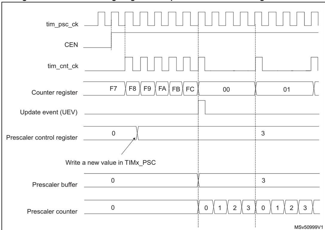
Figure 469 is a timing diagram illustrating the counter behavior when the prescaler division is changed from 1 to 4. The diagram shows the following signals and their states over time:
- tim_psc_ck : A high-frequency clock signal.
- CEN : Counter Enable signal, which is active low. It is shown as a high level.
- tim_cnt_ck : The counter clock signal, which is derived from tim_psc_ck.
- Counter register : Shows the counter values: F7, F8, F9, FA, FB, FC, 00, 01.
- Update event (UEV) : A pulse that occurs when the counter reaches FC and rolls over to 00.
- Prescaler control register : Shows the prescaler division value. It is initially 0 (division by 1) and is changed to 3 (division by 4) by writing a new value in TIMx_PSC.
- Prescaler buffer : Shows the prescaler division value that is actually used by the counter. It is initially 0 and is updated to 3 when the UEV occurs.
- Prescaler counter : Shows the prescaler counter values. It counts 0, 1, 2, 3, 0, 1, 2, 3, which corresponds to a division by 4.
MSv50999V1
31.4.4 Counter modes
Upcounting mode
In upcounting mode, the counter counts from 0 to the autoreload value (content of the TIMx_ARR register), then restarts from 0 and generates a counter overflow event.
If the repetition counter is used, the update event (UEV) is generated after upcounting is repeated for the number of times programmed in the repetition counter register (TIMx_RCR). Else the update event is generated at each counter overflow.
Setting the UG bit in the TIMx_EGR register (by software or by using the slave mode controller) also generates an update event.
The UEV event can be disabled by software by setting the UDIS bit in the TIMx_CR1 register. This is to avoid updating the shadow registers while writing new values in the preload registers. Then no update event occurs until the UDIS bit has been written to 0. However, the counter restarts from 0, as well as the counter of the prescaler (but the prescale rate does not change). In addition, if the URS bit (update request selection) in TIMx_CR1 register is set, setting the UG bit generates an update event UEV but without setting the UIF flag (thus no interrupt or DMA request is sent). This is to avoid generating both update and capture interrupts when clearing the counter on the capture event.
When an update event occurs, all the registers are updated and the update flag (UIF bit in TIMx_SR register) is set (depending on the URS bit):
- • The repetition counter is reloaded with the content of TIMx_RCR register,
- • The autoreload shadow register is updated with the preload value (TIMx_ARR),
- • The buffer of the prescaler is reloaded with the preload value (content of the TIMx_PSC register).
The following figures show some examples of the counter behavior for different clock frequencies when TIMx_ARR = 0x36.
Figure 470. Counter timing diagram, internal clock divided by 1
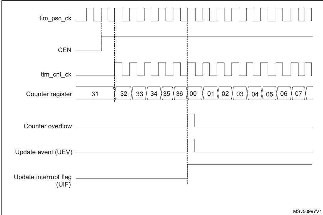
This timing diagram illustrates the operation of a general-purpose timer with the internal clock divided by 1. The top signal, tim_psc_ck , is a periodic square wave. Below it, CEN (Counter Enable) is shown as a high-level signal. The tim_cnt_ck signal is a square wave with a frequency twice that of tim_psc_ck . The Counter register displays a sequence of values: 31, 32, 33, 34, 35, 36, 00, 01, 02, 03, 04, 05, 06, 07. Vertical dashed lines indicate clock edges. At the transition from 36 to 00, the Counter overflow signal pulses high. Simultaneously, the Update event (UEV) and the Update interrupt flag (UIF) also pulse high. The diagram is labeled MSv50997V1 in the bottom right corner.
Figure 471. Counter timing diagram, internal clock divided by 2
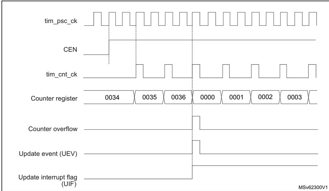
This timing diagram illustrates the operation of a general-purpose timer with the internal clock divided by 2. The tim_psc_ck signal is a periodic square wave. CEN is a high-level signal. The tim_cnt_ck signal is a square wave with a frequency equal to tim_psc_ck . The Counter register displays a sequence of values: 0034, 0035, 0036, 0000, 0001, 0002, 0003. Vertical dashed lines indicate clock edges. At the transition from 0036 to 0000, the Counter overflow signal pulses high. Simultaneously, the Update event (UEV) and the Update interrupt flag (UIF) also pulse high. The diagram is labeled MSv62300V1 in the bottom right corner.
Figure 472. Counter timing diagram, internal clock divided by 4
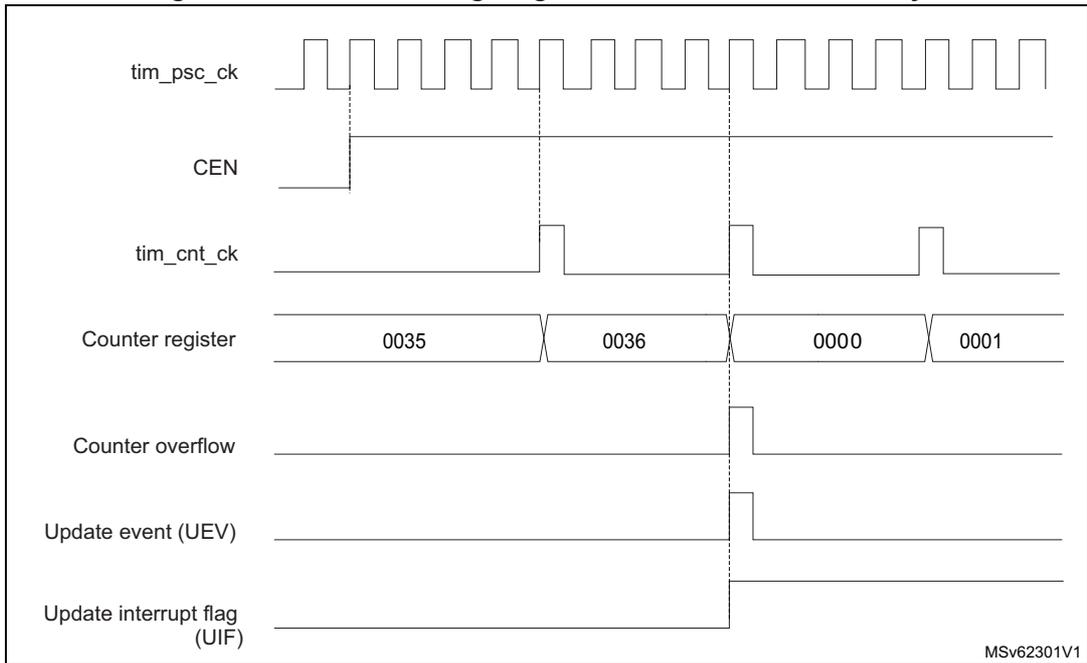
This timing diagram illustrates the operation of a timer when the internal clock is divided by 4. The top signal, tim_psc_ck , is a high-frequency square wave. Below it, the CEN (Counter Enable) signal is shown as a horizontal line that goes high at the start. The tim_cnt_ck signal is a lower-frequency square wave, which is the tim_psc_ck divided by 4. Vertical dashed lines indicate the rising edges of tim_cnt_ck . The Counter register shows a sequence of values: 0035, 0036, 0000, and 0001. The transition from 0036 to 0000 occurs at the second rising edge of tim_cnt_ck after CEN goes high, indicating an overflow. At this same edge, the Counter overflow , Update event (UEV) , and Update interrupt flag (UIF) signals all go high. The identifier MSv62301V1 is in the bottom right corner.
Figure 473. Counter timing diagram, internal clock divided by N
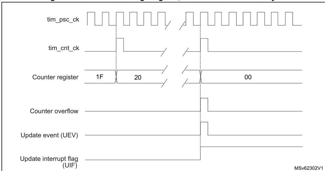
This timing diagram illustrates the operation of a timer when the internal clock is divided by an arbitrary value N. The top signal, tim_psc_ck , is a square wave. The tim_cnt_ck signal is a square wave with a period N times that of tim_psc_ck . Vertical dashed lines indicate the rising edges of tim_cnt_ck . The Counter register shows values 1F, 20, and 00. The transition from 20 to 00 occurs at the second rising edge of tim_cnt_ck after the start, indicating an overflow. At this same edge, the Counter overflow , Update event (UEV) , and Update interrupt flag (UIF) signals all go high. The identifier MSv62302V1 is in the bottom right corner.
Figure 474. Counter timing diagram, update event when ARPE = 0 (TIMx_ARR not preloaded)
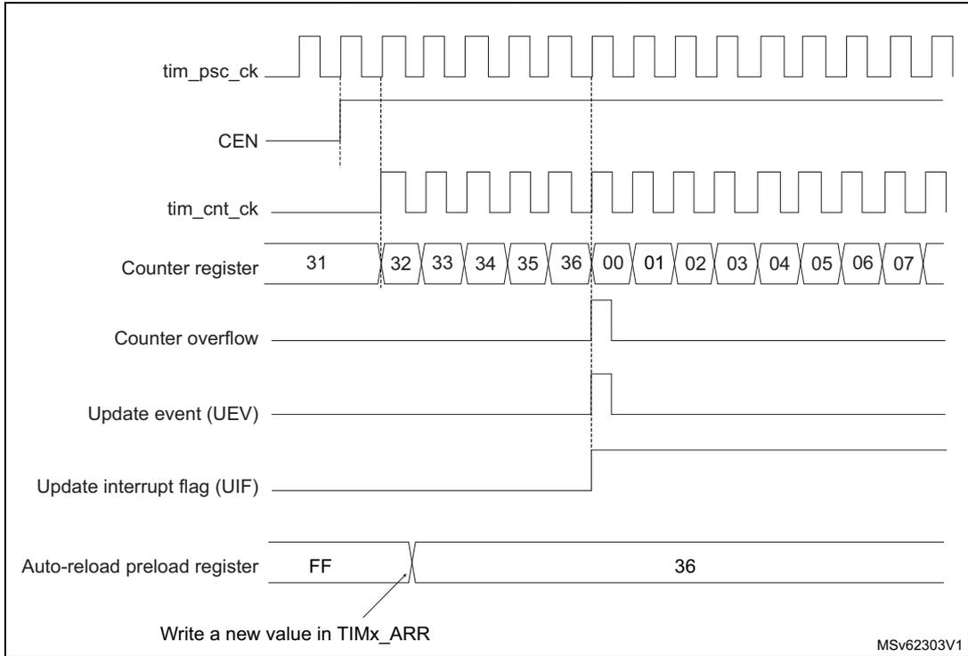
The timing diagram illustrates the operation of a general-purpose timer. The tim_psc_ck signal is a periodic clock. The CEN (Counter Enable) signal is shown as a dashed line that goes high to enable the counter. The tim_cnt_ck signal is the counter clock, which is a divided version of the prescaler clock. The Counter register shows a sequence of values: 31, 32, 33, 34, 35, 36, 00, 01, 02, 03, 04, 05, 06, 07. The Counter overflow signal is a pulse that goes high when the counter reaches 36 and resets to 00. The Update event (UEV) and Update interrupt flag (UIF) are also pulses that go high at the overflow point. The Auto-reload preload register shows a value of FF (hex) being written, which is then updated to 36. An arrow points to the register with the text "Write a new value in TIMx_ARR". The diagram is labeled MSV62303V1.
Figure 475. Counter timing diagram, update event when ARPE = 1
(TIMx_ARR preloaded)
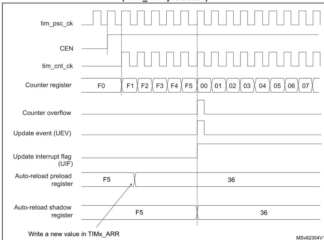
The timing diagram illustrates the operation of a general purpose timer when ARPE = 1 and the auto-reload register (TIMx_ARR) is preloaded. The signals shown are:
- tim_psc_ck : Prescaler clock signal, a periodic square wave.
- CEN : Counter enable signal, which is high to enable counting.
- tim_cnt_ck : Counter clock signal, derived from the prescaler clock.
- Counter register : Shows the sequence of counter values: F0, F1, F2, F3, F4, F5, 00, 01, 02, 03, 04, 05, 06, 07. The values F0 through F5 are shown before the reset to 00.
- Counter overflow : A pulse generated when the counter reaches its maximum value (00 in this sequence).
- Update event (UEV) : A pulse generated when the counter overflows and ARPE = 1.
- Update interrupt flag (UIF) : A pulse generated when the update event occurs.
- Auto-reload preload register : Shows the value F5 being written (indicated by an arrow and the text "Write a new value in TIMx_ARR") and then the value 36 being loaded.
- Auto-reload shadow register : Shows the value F5 being loaded and then the value 36 being loaded.
MSV62304V1
31.4.5 Repetition counter
Section 31.4.3: Time-base unit describes how the update event (UEV) is generated with respect to the counter overflows. It is actually generated only when the repetition counter has reached zero. This can be useful when generating PWM signals.
This means that data are transferred from the preload registers to the shadow registers (TIMx_ARR autoreload register, TIMx_PSC prescaler register, but also TIMx_CCRx capture/compare registers in compare mode) every N counter overflows, where N is the value in the TIMx_RCR repetition counter register.
The repetition counter is decremented at each counter overflow.
The repetition counter is an autoreload type; the repetition rate is maintained as defined by the TIMx_RCR register value (refer to Figure 476 ). When the update event is generated by software (by setting the UG bit in TIMx_EGR register) or by hardware through the slave mode controller, it occurs immediately whatever the value of the repetition counter is and the repetition counter is reloaded with the content of the TIMx_RCR register.
Figure 476. Update rate examples depending on mode and TIMx_RCR register settings
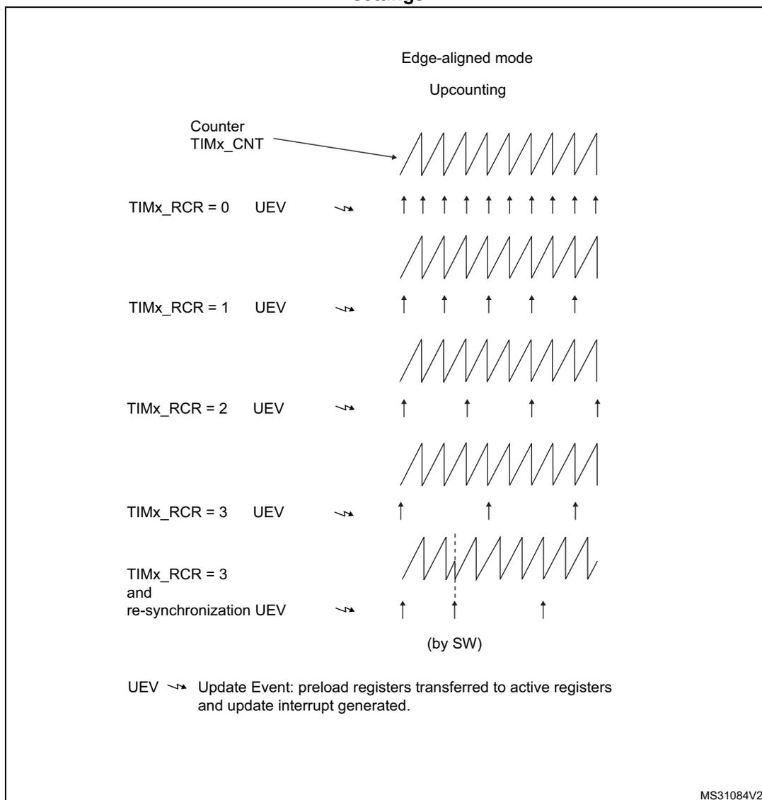
Edge-aligned mode
Upcounting
Counter TIMx_CNT
TIMx_RCR = 0 UEV
TIMx_RCR = 1 UEV
TIMx_RCR = 2 UEV
TIMx_RCR = 3 UEV
TIMx_RCR = 3 and re-synchronization UEV
(by SW)
UEV Update Event: preload registers transferred to active registers and update interrupt generated.
MS31084V2
31.4.6 Clock selection
The counter clock can be provided by the following clock sources:
- • Internal clock (tim_ker_ck)
- • External clock mode1: external input pin (tim_ti1 or tim_ti2, if available)
- • Internal trigger inputs (tim_itrx) (only for TIM15): using one timer as the prescaler for another timer, for example, TIM1 can be configured to act as a prescaler for TIM15. Refer to Using one timer as prescaler for another timer for more details.
Internal clock source (tim_ker_ck)
If the slave mode controller is disabled (SMS = 000), then the CEN (in the TIMx_CR1 register) and UG bits (in the TIMx_EGR register) are actual control bits and can be changed
only by software (except UG which remains cleared automatically). As soon as the CEN bit is written to 1, the prescaler is clocked by the internal clock tim_ker_ck.
Figure 477 shows the behavior of the control circuit and the upcounter in normal mode, without prescaler.
Figure 477. Control circuit in normal mode, internal clock divided by 1
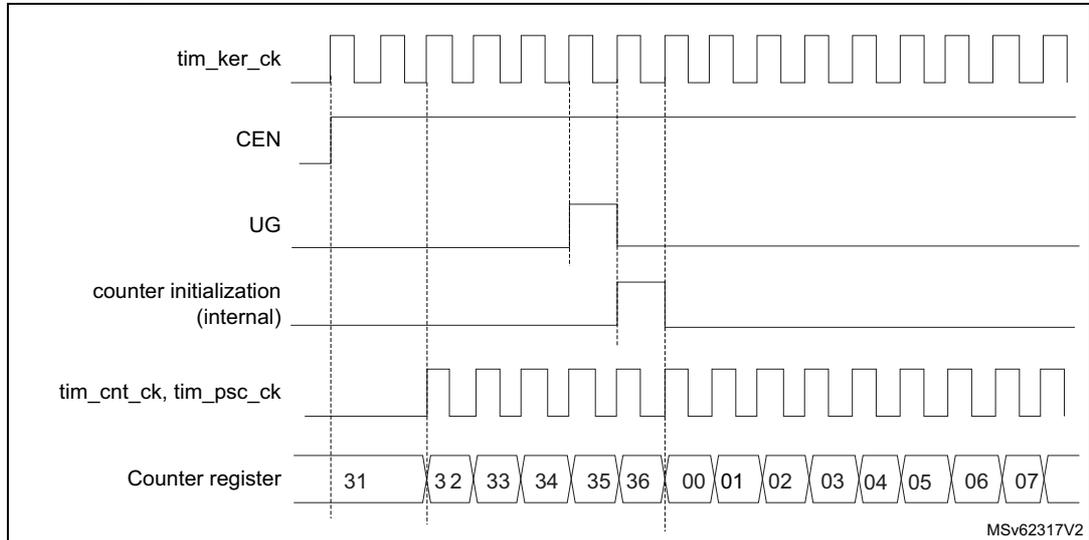
The diagram shows the relationship between control signals and the counter register.
-
tim_ker_ck
: A continuous square wave representing the internal clock.
-
CEN
: Counter Enable signal, held high throughout the sequence.
-
UG
: Update Generation signal, which pulses low briefly to trigger an update.
-
counter initialization (internal)
: A signal that pulses low at the same time as UG.
-
tim_cnt_ck, tim_psc_ck
: The clock for the counter and prescaler, which is active only when CEN is high.
-
Counter register
: Shows the count sequence: 31, 32, 33, 34, 35, 36, followed by a rollover to 00, 01, 02, 03, 04, 05, 06, 07. Vertical dashed lines indicate the clock edges that cause the count to increment.
External clock source mode 1
This mode is selected when SMS = 111 in the TIMx_SMCR register. The counter can count at each rising or falling edge on a selected input.
Figure 478. tim_ti2 external clock connection example
This block diagram illustrates the external clock source mode 1 configuration.
-
TIMx_TISEL
(TI2SEL[3:0]) selects the input source for TIM_CH2.
-
TIM_CH2
input can be
tim_ti2_in0
or
tim_ti2_in[15:1]
.
- The signal passes through a
Filter
(controlled by
ICF[3:0]
in
TIMx_CCMR1
) and an
Edge detector
(controlled by
CC2P
in
TIMx_CCER
).
- The edge detector outputs
tim_ti2f_rising
and
tim_ti2f_falling
signals.
- These signals are multiplexed (0 for rising, 1 for falling) and fed into the
TIMx_SMCR
register's
TS[4:0]
input.
- The
TIMx_SMCR
register also has options:
tim_itrx
(000xx),
tim_ti1f_ed
(00100),
tim_ti1fp2
(00101), and
tim_ti2_fp2
(00110).
- The selected signal becomes
tim_trgi
(trigger input).
-
tim_trgi
is connected to the
External clock mode 1
block.
- This block also receives
tim_ker_ck
(internal clock) and is controlled by
SMS[2:0]
in
TIMx_SMCR
.
- The output of this block is
tim_psc_ck
(prescaler clock).
For example, to configure the upcounter to count in response to a rising edge on the tim_ti2 input, use the following procedure:
- 1. Select the proper
tim_ti2_in[15:0]source (internal or external) with theTI2SEL[3:0]bits in theTIMx_TISELregister. - 2. Configure channel 2 to detect rising edges on the
tim_ti2input by writingCC2S = 01in theTIMx_CCMR1register. - 3. Configure the input filter duration by writing the
IC2F[3:0]bits in theTIMx_CCMR1register (if no filter is needed, keepIC2F = 0000). - 4. Select rising edge polarity by writing
CC2P = 0in theTIMx_CCERregister. - 5. Configure the timer in external clock mode 1 by writing
SMS = 111in theTIMx_SMCRregister. - 6. Select
tim_ti2as the trigger input source by writingTS = 00110in theTIMx_SMCRregister. - 7. Enable the counter by writing
CEN = 1in theTIMx_CR1register.
Note: The capture prescaler is not used for triggering, it is not necessary to configure it.
When a rising edge occurs on
tim_ti2
, the counter counts once and the
TIF
flag is set.
The delay between the rising edge on
tim_ti2
and the actual clock of the counter is due to the resynchronization circuit on
tim_ti2
input.
Figure 479. Control circuit in external clock mode 1
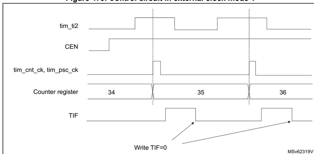
The diagram illustrates the timing relationships in external clock mode 1. The
tim_ti2
signal is a periodic square wave. The
CEN
signal is a horizontal line indicating the counter is enabled. The
tim_cnt_ck, tim_psc_ck
signal shows pulses that occur at the rising edges of
tim_ti2
. The
Counter register
shows values 34, 35, and 36, with increments occurring at the rising edges of
tim_ti2
. The
TIF
signal is a pulse that goes high at each rising edge of
tim_ti2
and is cleared by writing
TIF=0
.
31.4.7 Capture/compare channels
Each Capture/Compare channel is built around a capture/compare register (including a shadow register), a input stage for capture (with digital filter, multiplexing and prescaler) and an output stage (with comparator and output control).
Figure 480 to Figure 483 give an overview of one Capture/Compare channel.
The input stage samples the corresponding
tim_tix
input to generate a filtered signal
tim_tixf
. Then, an edge detector with polarity selection generates a signal (
tim_tixfpy
) which can be used as trigger input by the slave mode controller or as the capture command. It is prescaled before the capture register (
ICxPS
).
Figure 480. Capture/compare channel (example: channel 1 input stage)
![Figure 480: Capture/compare channel (example: channel 1 input stage) block diagram. The diagram shows the input stage for channel 1. Inputs include TIM_CH1, tim_ti1_in0, and tim_ti1_in[15:1]. These pass through a 'Filter downcounter' (controlled by fots and ICF[3:0] from TIMx_CCMR1) to produce tim_ti1f. This signal goes to an 'Edge detector' which outputs tim_ti1f_rising and tim_ti1f_falling. These signals are multiplexed (0 for rising, 1 for falling) and then combined with tim_ti2f_rising and tim_ti2f_falling (from channel 2) via another multiplexer (0 for rising, 1 for falling). The output of this mux is tim_ti1_fp1. This signal is then multiplexed (01 for tim_ti1_fp1, 10 for tim_ti2fp1, 11 for tim_trc from slave mode controller) to produce tim_ic1. tim_ic1 is then divided by a 'Divider /1, /2, /4, /8' (controlled by CC1S[1:0], ICPS[1:0], and CC1E from TIMx_CCMR1 and TIMx_CCER) to produce tim_ic1f. An OR gate combines tim_ti1f_rising and tim_ti1f_falling to produce tim_ti1f_ed, which is sent to the slave mode controller. Source: MSV62322V2.](/RM0440-STM32G4/ca4c9217d81aa05aaaeb56a372a8611b_img.jpg)
The output stage generates an intermediate waveform which is then used for reference: tim_ocxref (active high). The polarity acts at the end of the chain.
Figure 481. Capture/compare channel 1 main circuit
![Figure 481: Capture/compare channel 1 main circuit block diagram. The diagram shows the main circuit for channel 1. It is connected to an APB Bus via an MCU-peripheral interface. The interface controls a 16/32-bit 'Capture/compare preload register' and a 'compare shadow register'. These registers are connected to a 'Counter'. The Counter output is compared with CCR1 in a 'Comparator' to produce CNT>CCR1 and CNT=CCR1 signals. In 'Input mode', the Counter output is captured into the preload register. Control signals for input mode include CC1S[1], CC1S[0], IC1PS, CC1E, CC1G, and TIMx_EGR. In 'Output mode', the preload register value is transferred to the shadow register, which then controls an output stage. Control signals for output mode include CC1S[1], CC1S[0], OC1PE, and TIMx_CCMR1. A 'UEV (from time base unit)' signal is also used in the output mode. Source: MSV63030V1.](/RM0440-STM32G4/ffac88b48793a7450f4fd9b2d28d560c_img.jpg)
Figure 482. Output stage of capture/compare channel (channel 1)
![Figure 482: Output stage of capture/compare channel (channel 1). This block diagram shows the internal logic for channel 1 output (tim_oc1). It starts with a counter (CNT) and compare register (CCR1) inputs. An 'Output mode controller' takes CNT>CCR1 and CNT=CCR1 signals, along with OC1CE and OC1M[3:0] from TIMx_CCMR1, to produce tim_oc1ref. This signal goes to an 'Output selector' and a 'Dead-time generator'. The dead-time generator also takes DTG[7:0] from TIMx_BDTR and produces tim_oc1n_dt. The output selector produces a signal that goes through a multiplexer (CC1P) controlled by TIMx_CCER (CC1NE, CC1E, CC1NP) and then through an inverter to an 'Output enable circuit'. The enable circuit also takes MOE, OSSI, OSSR from TIMx_BDTR and OIS1, OIS1N from TIMx_CR2. The final output is tim_oc1. A reference signal tim_ocref_clr_int is also shown.](/RM0440-STM32G4/0c6b5f44790550c9d80ecb3d57f03711_img.jpg)
Figure 483. Output stage of capture/compare channel (channel 2 for TIM15)
![Figure 483: Output stage of capture/compare channel (channel 2 for TIM15). This block diagram shows the internal logic for channel 2 output (tim_oc2) for TIM15. It starts with a counter (CNT) and compare register (CCR2) inputs. An 'Output mode controller' takes CNT>CCR2 and CNT=CCR2 signals, along with OC2CE and OC2M[3:0] from TIMx_CCMR1, to produce tim_oc2ref. This signal goes to an 'Output selector' and a 'Dead-time generator'. The dead-time generator also takes DTG[7:0] from TIMx_BDTR and produces tim_oc2n_dt. The output selector produces a signal that goes through a multiplexer (CC2E) controlled by TIMx_CCER (CC2E) and then through an inverter to an 'Output enable circuit'. The enable circuit also takes CC2E from TIMx_CCER and OIS2 from TIMx_CR2. The final output is tim_oc2. Reference signals tim_ocref_clr_int and tim_oc1ref are also shown.](/RM0440-STM32G4/a6b76109c3dbf84b09d71173da026c74_img.jpg)
The capture/compare block is made of one preload register and one shadow register. Write and read always access the preload register.
In capture mode, captures are actually done in the shadow register, which is copied into the preload register.
In compare mode, the content of the preload register is copied into the shadow register which is compared to the counter.
31.4.8 Input capture mode
In Input capture mode, the capture/compare registers (TIMx_CCRx) are used to latch the value of the counter after a transition detected by the corresponding tim_icx signal. When a capture occurs, the corresponding CCxIF flag (TIMx_SR register) is set and an interrupt or a DMA request can be sent if they are enabled. If a capture occurs while the CCxIF flag was
already high, then the overcapture flag CCxOF (TIMx_SR register) is set. CCxIF can be cleared by software by writing it to 0 or by reading the captured data stored in the TIMx_CCRx register. CCxOF is cleared when it is written with 0.
The following example shows how to capture the counter value in TIMx_CCR1 when tim_ti1 input rises. To do this, use the following procedure:
- 1. Select the proper tim_ti1_in[15:1] source (internal or external) with the TI1SEL[3:0] bits in the TIMx_TISEL register.
- 2. Select the active input: TIMx_CCR1 must be linked to the tim_ti1 input, so write the CC1S bits to 01 in the TIMx_CCMR1 register. As soon as CC1S becomes different from 00, the channel is configured in input, and the TIMx_CCR1 register becomes read-only.
- 3. Program the appropriate input filter duration in relation with the signal connected to the timer (when the input is one of the tim_tix (ICxF bits in the TIMx_CCMRx register). Let's imagine that, when toggling, the input signal is not stable during at least 5 internal clock cycles. The user must program a filter duration longer than these five clock cycles. The user can validate a transition on tim_ti1 when eight consecutive samples with the new level have been detected (sampled at \( f_{DTS} \) frequency). Then write IC1F bits to 0011 in the TIMx_CCMR1 register.
- 4. Select the edge of the active transition on the tim_ti1 channel by writing CC1P bit to 0 in the TIMx_CCER register (rising edge in this case).
- 5. Program the input prescaler. In this example, the user wants the capture to be performed at each valid transition, so the prescaler is disabled (write IC1PS bits to 00 in the TIMx_CCMR1 register).
- 6. Enable capture from the counter into the capture register by setting the CC1E bit in the TIMx_CCER register.
- 7. If needed, enable the related interrupt request by setting the CC1IE bit in the TIMx_DIER register, and/or the DMA request by setting the CC1DE bit in the TIMx_DIER register.
When an input capture occurs:
- • The TIMx_CCR1 register gets the value of the counter on the active transition.
- • CC1IF flag is set (interrupt flag). CC1OF is also set if at least two consecutive captures occurred whereas the flag was not cleared.
- • An interrupt is generated depending on the CC1IE bit.
- • A DMA request is generated depending on the CC1DE bit.
In order to handle the overcapture, it is recommended to read the data before the overcapture flag. This is to avoid missing an overcapture which may happen after reading the flag and before reading the data.
Note: IC interrupt and/or DMA requests can be generated by software by setting the corresponding CCxG bit in the TIMx_EGR register.
31.4.9 PWM input mode (only for TIM15)
This mode is used to measure both the period and the duty cycle of a PWM signal connected to single tim_tix input:
- • The TIMx_CCR1 register holds the period value (interval between two consecutive rising edges)
- • The TIMx_CCR2 register holds the pulse width (interval between two consecutive rising and falling edges)
This mode is a particular case of input capture mode. The set-up procedure is similar with the following differences:
- • Two tim_icx signals are mapped on the same tim_tix input.
- • These two tim_icx signals are active on edges with opposite polarity.
- • One of the two tim_tixfpy signals is selected as trigger input and the slave mode controller is configured in reset mode.
For example, one can measure the period (in TIMx_CCR1 register) and the duty cycle (in TIMx_CCR2 register) of the PWM applied on tim_ti1 using the following procedure (depending on tim_ker_ck frequency and prescaler value):
- 1. Select the proper tim_ti1_in[15:0] source (internal or external) with the TI1SEL[3:0] bits in the TIMx_TISEL register.
- 2. Select the active input for TIMx_CCR1: write the CC1S bits to 01 in the TIMx_CCMR1 register (tim_ti1 selected).
- 3. Select the active polarity for tim_ti1fp1 (used both for capture in TIMx_CCR1 and counter clear): write the CC1P and CC1NP bits to 0 (active on rising edge).
- 4. Select the active input for TIMx_CCR2: write the CC2S bits to 10 in the TIMx_CCMR1 register (tim_ti1 selected).
- 5. Select the active polarity for tim_ti1fp2 (used for capture in TIMx_CCR2): write the CC2P and CC2NP bits to 10 (active on falling edge).
- 6. Select the valid trigger input: write the TS bits to 00101 in the TIMx_SMCR register (tim_ti1fp1 selected).
- 7. Configure the slave mode controller in reset mode: write the SMS bits to 100 in the TIMx_SMCR register.
- 8. Enable the captures: write the CC1E and CC2E bits to 1 in the TIMx_CCER register.
Figure 484. PWM input mode timing
- 1. The PWM input mode can be used only with the TIMx_CH1/TIMx_CH2 signals due to the fact that only tim_ti1fp1 and tim_ti2fp2 are connected to the slave mode controller.
31.4.10 Forced output mode
In output mode (CCxS bits = 00 in the TIMx_CCMRx register), each output compare signal (tim_ocxref and then tim_ocx/tim_ocxn) can be forced to active or inactive level directly by software, independently of any comparison between the output compare register and the counter.
To force an output compare signal (tim_ocxref/tim_ocx) to its active level, one just needs to write 101 in the OCxM bits in the corresponding TIMx_CCMRx register. Thus tim_ocxref is forced high (tim_ocxref is always active high) and tim_ocx get opposite value to CCxP polarity bit.
For example: CCxP = 0 (tim_ocx active high) → tim_ocx is forced to high level.
The tim_ocxref signal can be forced low by writing the OCxM bits to 100 in the TIMx_CCMRx register.
Anyway, the comparison between the TIMx_CCRx shadow register and the counter is still performed and allows the flag to be set. Interrupt and DMA requests can be sent accordingly. This is described in the output compare mode section below.
31.4.11 Output compare mode
This function is used to control an output waveform or indicating when a period of time has elapsed.
When a match is found between the capture/compare register and the counter, the output compare function:
- • Assigns the corresponding output pin to a programmable value defined by the output compare mode (OCxM bits in the TIMx_CCMRx register) and the output polarity (CCxP bit in the TIMx_CCER register). The output pin can keep its level (OCXM = 000), be set
active (OCxM = 001), be set inactive (OCxM = 010) or can toggle (OCxM = 011) on match.
- • Sets a flag in the interrupt status register (CCxIF bit in the TIMx_SR register).
- • Generates an interrupt if the corresponding interrupt mask is set (CCxIE bit in the TIMx_DIER register).
- • Sends a DMA request if the corresponding enable bit is set (CCxDE bit in the TIMx_DIER register, CCDS bit in the TIMx_CR2 register for the DMA request selection).
The TIMx_CCRx registers can be programmed with or without preload registers using the OCxPE bit in the TIMx_CCMRx register.
In output compare mode, the update event UEV has no effect on tim_ocxref and tim_ocx output. The timing resolution is one count of the counter. Output compare mode can also be used to output a single pulse (in One-pulse mode).
Procedure
- 1. Select the counter clock (internal, external, prescaler).
- 2. Write the desired data in the TIMx_ARR and TIMx_CCRx registers.
- 3. Set the CCxIE bit if an interrupt request is to be generated.
- 4. Select the output mode. For example:
- – Write OCxM = 011 to toggle tim_ocx output pin when CNT matches CCRx
- – Write OCxPE = 0 to disable preload register
- – Write CCxP = 0 to select active high polarity
- – Write CCxE = 1 to enable the output
- 5. Enable the counter by setting the CEN bit in the TIMx_CR1 register.
The TIMx_CCRx register can be updated at any time by software to control the output waveform, provided that the preload register is not enabled (OCxPE = 0, else TIMx_CCRx shadow register is updated only at the next update event UEV). An example is given in Figure 485 .
Figure 485. Output compare mode, toggle on tim_oc1
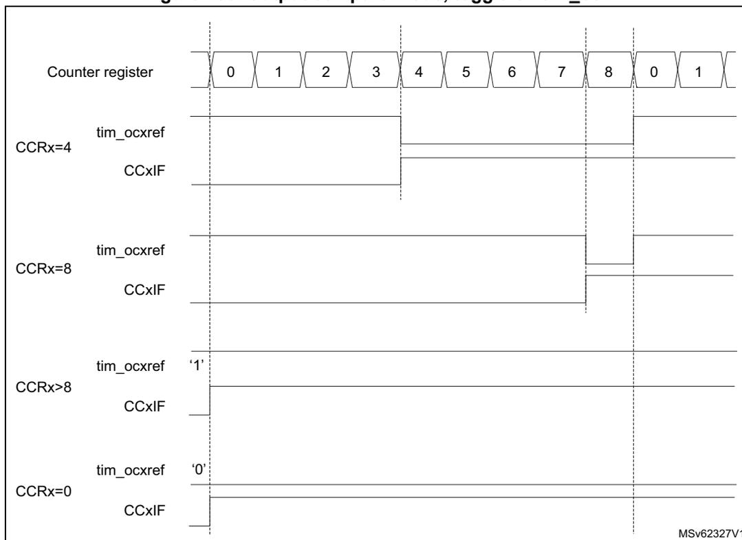
The figure is a timing diagram illustrating the output compare mode, toggle on tim_oc1. It shows the relationship between the Counter register, the tim_ocref output signal, and the CCxIF flag for different compare register (CCRx) values.
The Counter register values are shown at the top: 0, 1, 2, 3, 4, 5, 6, 7, 8, 0, 1. Vertical dashed lines indicate the points where the counter value matches the compare value (CCRx).
Four scenarios are shown:
- CCRx=4: The tim_ocref signal is high from counter 0 to 3 and low from 4 to 7. The CCxIF flag is set at counter 4.
- CCRx=8: The tim_ocref signal is high from 0 to 7 and low at 8. The CCxIF flag is set at counter 8.
- CCRx>8: The tim_ocref signal is always high ('1'). The CCxIF flag is never set.
- CCRx=0: The tim_ocref signal is always low ('0'). The CCxIF flag is never set.
MSv62327V1
31.4.12 PWM mode
Pulse width modulation mode is used to generate a signal with a frequency determined by the value of the TIMx_ARR register and a duty cycle determined by the value of the TIMx_CCRx register.
The PWM mode can be selected independently on each channel (one PWM per tim_ocx output) by writing 110 (PWM mode 1) or 111 (PWM mode 2) in the OCxM bits in the TIMx_CCMRx register. The corresponding preload register must be enabled by setting the OCxPE bit in the TIMx_CCMRx register, and eventually the autoreload preload register (in upcounting or center-aligned modes) by setting the ARPE bit in the TIMx_CR1 register.
As the preload registers are transferred to the shadow registers only when an update event occurs, before starting the counter, all registers must be initialized by setting the UG bit in the TIMx_EGR register.
tim_ocx polarity is software programmable using the CCxP bit in the TIMx_CCER register. It can be programmed as active high or active low. tim_ocx output is enabled by a combination of the CCxE, CCxNE, MOE, OSSI, and OSSR bits (TIMx_CCER and TIMx_BDTR registers). Refer to the TIMx_CCER register description for more details.
In PWM mode (1 or 2), TIMx_CNT and TIMx_CCRx are always compared to determine whether \( TIMx\_CCRx \leq TIMx\_CNT \) or \( TIMx\_CNT \leq TIMx\_CCRx \) (depending on the direction of the counter).
The TIM15/TIM16/TIM17 are capable of upcounting only. Refer to Upcounting mode .
In the following example applies to PWM mode 1. The reference PWM signal tim_ocref is high as long as \( TIMx\_CNT < TIMx\_CCRx \) else it becomes low. If the compare value in
TIMx_CCRx is greater than the autoreload value (in TIMx_ARR) then tim_ocxref is held at 1. If the compare value is 0 then tim_ocxref is held at 0. Figure 486 shows some edge-aligned PWM waveforms in an example where TIMx_ARR = 8.
Figure 486. Edge-aligned PWM waveforms (ARR = 8)
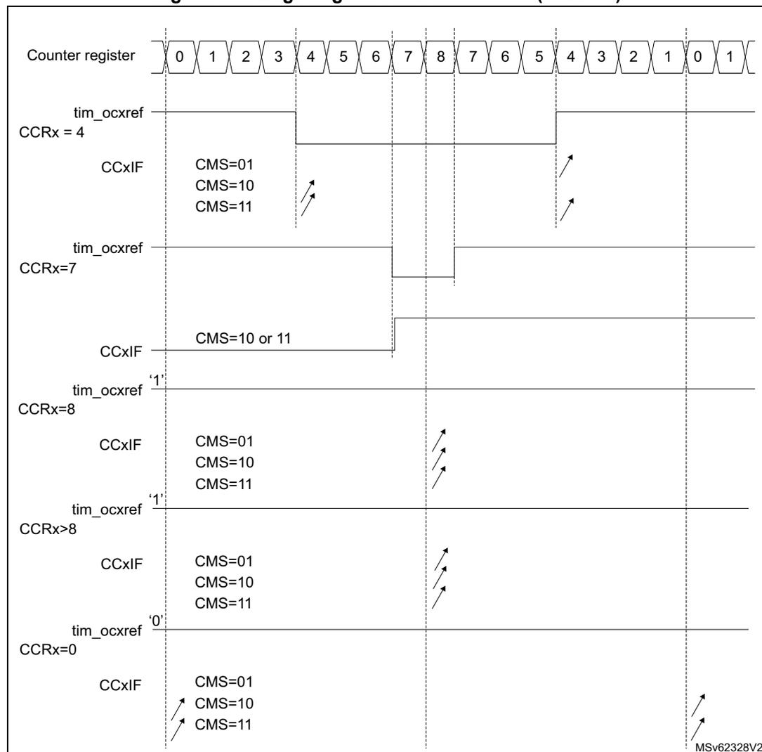
The figure illustrates the relationship between the counter register, the output compare register (CCR), and the output compare signal (tim_ocxref) for edge-aligned PWM mode. The counter register sequence is: 0, 1, 2, 3, 4, 5, 6, 7, 8, 7, 6, 5, 4, 3, 2, 1, 0, 1. Vertical dashed lines mark the counter values 0, 4, 7, 8, 7, 6, 5, 4, 3, 2, 1, 0, 1.
- CCRx = 4: The tim_ocxref signal is high from counter 0 to 4, then low until 8, then high again. The CCxIF flag is shown for CMS=01, CMS=10, and CMS=11, with rising edges at counter values 4 and 8.
- CCRx = 7: The tim_ocxref signal is high from counter 0 to 7, then low until 8, then high again. The CCxIF flag is shown for CMS=10 or 11, with a rising edge at counter value 7.
- CCRx = 8: The tim_ocxref signal is high from counter 0 to 8, then low until 8, then high again. The CCxIF flag is shown for CMS=01, CMS=10, and CMS=11, with rising edges at counter value 8.
- CCRx > 8: The tim_ocxref signal is held at '1' (high) throughout the cycle. The CCxIF flag is shown for CMS=01, CMS=10, and CMS=11, with rising edges at counter value 8.
- CCRx = 0: The tim_ocxref signal is held at '0' (low) throughout the cycle. The CCxIF flag is shown for CMS=01, CMS=10, and CMS=11, with rising edges at counter values 0 and 8.
MSV62328V2
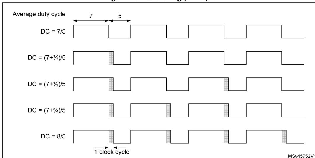
Dithering mode
The PWM mode effective resolution can be increased by enabling the dithering mode, using the DITHEN bit in the TIMx_CR1 register. This applies to both the CCR (for duty cycle resolution increase) and ARR (for PWM frequency resolution increase).
The operating principle is to have the actual CCR (or ARR) value slightly changed (adding or not one timer clock period) over 16 consecutive PWM periods, with predefined patterns. This allows a 16-fold resolution increase, considering the average duty cycle or PWM period. The Figure 487 below presents the dithering principle applied to four consecutive PWM cycles.
Figure 487. Dithering principle
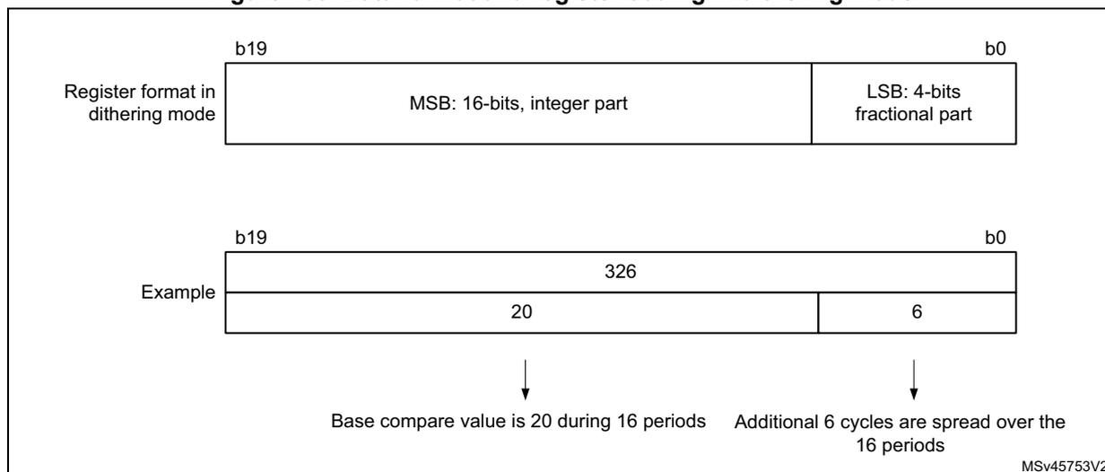
When the dithering mode is enabled, the register coding is changed as follows (see Figure 488 for example):
- • The four LSBs are coding for the enhanced resolution part (fractional part).
- • The MSBs are left-shifted to the bits 19:4 and are coding for the base value.
Note: The ARR and CCR values will be updated automatically if the DITHEN bit is set / reset (for instance, if ARR = 0x05 with DITHEN = 0, it will be updated to ARR = 0x50 with DITHEN = 1). The following sequence must be followed when resetting the DITHEN bit:
- 1. CEN and ARPE bits must be reset
- 2. The ARR[3:0] bits must be reset
- 3. The DITHEN bit must be reset
- 4. The CCIF flags must be cleared
- 5. The CEN bit can be set (eventually with ARPE = 1).
Figure 488. Data format and register coding in dithering mode
The minimum frequency is given by the following formula:
Note: The maximum TIMx_ARR and TIMxCCRy values are limited to 0xFFFEF in dithering mode (corresponds to 65534 for the integer part and 15 for the dithered part).
As shown on the Figure 489 below, the dithering mode is used to increase the PWM resolution whatever the PWM frequency.
Figure 489. PWM resolution vs frequency
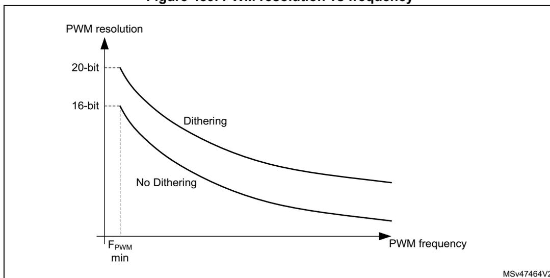
The graph illustrates the relationship between PWM resolution and PWM frequency. The y-axis represents PWM resolution, with markers for 20-bit and 16-bit. The x-axis represents PWM frequency, with a marker for \( F_{\text{PWM min}} \) . Two curves are plotted: 'Dithering' and 'No Dithering'. The 'Dithering' curve starts at a higher resolution (20-bit) and decreases as frequency increases. The 'No Dithering' curve starts at a lower resolution (16-bit) and also decreases as frequency increases. A vertical dashed line indicates the minimum PWM frequency, \( F_{\text{PWM min}} \) .
The duty cycle and/or period changes are spread over 16 consecutive periods, as described in the Figure 490 below.
Figure 490. PWM dithering pattern
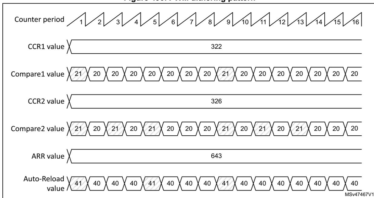
The autoreload and compare values increments are spread following specific patterns described in the Table 311 below. The dithering sequence is done to have increments distributed as evenly as possible and minimize the overall ripple.
Table 311. CCR and ARR register change dithering pattern
| - | PWM period | ||||||||||||||||
|---|---|---|---|---|---|---|---|---|---|---|---|---|---|---|---|---|---|
| LSB value | 1 | 2 | 3 | 4 | 5 | 6 | 7 | 8 | 9 | 10 | 11 | 12 | 13 | 14 | 15 | 16 | |
| 0000 | - | - | - | - | - | - | - | - | - | - | - | - | - | - | - | - | |
| 0001 | +1 | - | - | - | - | - | - | - | - | - | - | - | - | - | - | - | |
| 0010 | +1 | - | - | - | - | - | - | - | +1 | - | - | - | - | - | - | - | |
| 0011 | +1 | - | - | - | +1 | - | - | - | +1 | - | - | - | - | - | - | - | |
| 0100 | +1 | - | - | - | +1 | - | - | - | +1 | - | - | - | +1 | - | - | - | |
| 0101 | +1 | - | +1 | - | +1 | - | - | - | +1 | - | - | - | +1 | - | - | - | |
| 0110 | +1 | - | +1 | - | +1 | - | - | - | +1 | - | +1 | - | +1 | - | - | - | |
| 0111 | +1 | - | +1 | - | +1 | - | +1 | - | +1 | - | +1 | - | +1 | - | - | - | |
| 1000 | +1 | - | +1 | - | +1 | - | +1 | - | +1 | - | +1 | - | +1 | - | +1 | - | |
| 1001 | +1 | +1 | +1 | - | +1 | - | +1 | - | +1 | - | +1 | - | +1 | - | +1 | - | |
| 1010 | +1 | +1 | +1 | - | +1 | - | +1 | - | +1 | +1 | +1 | - | +1 | - | +1 | - | |
| 1011 | +1 | +1 | +1 | - | +1 | +1 | +1 | - | +1 | +1 | +1 | - | +1 | - | +1 | - | |
| 1100 | +1 | +1 | +1 | - | +1 | +1 | +1 | - | +1 | +1 | +1 | - | +1 | +1 | +1 | - | |
| 1101 | +1 | +1 | +1 | +1 | +1 | +1 | +1 | - | +1 | +1 | +1 | - | +1 | +1 | +1 | - | |
Table 311. CCR and ARR register change dithering pattern (continued)
| - | PWM period | ||||||||||||||||
|---|---|---|---|---|---|---|---|---|---|---|---|---|---|---|---|---|---|
| LSB value | 1 | 2 | 3 | 4 | 5 | 6 | 7 | 8 | 9 | 10 | 11 | 12 | 13 | 14 | 15 | 16 | |
| 1110 | +1 | +1 | +1 | +1 | +1 | +1 | +1 | - | +1 | +1 | +1 | +1 | +1 | +1 | +1 | - | |
| 1111 | +1 | +1 | +1 | +1 | +1 | +1 | +1 | +1 | +1 | +1 | +1 | +1 | +1 | +1 | +1 | - | |
31.4.13 Combined PWM mode (TIM15 only)
Combined PWM mode allows two edge or center-aligned PWM signals to be generated with programmable delay and phase shift between respective pulses. While the frequency is determined by the value of the TIMx_ARR register, the duty cycle and delay are determined by the two TIMx_CCRx registers. The resulting signals, tim_ocxrefc, are made of an OR or AND logical combination of two reference PWMs:
- • tim_oc1refc (or tim_oc2refc) is controlled by the TIMx_CCR1 and TIMx_CCR2 registers.
Combined PWM mode can be selected independently on two channels (one tim_ocx output per pair of CCR registers) by writing 1100 (Combined PWM mode 1) or 1101 (Combined PWM mode 2) in the OCxM bits in the TIMx_CCMRx register.
When a given channel is used as a combined PWM channel, its complementary channel must be configured in the opposite PWM mode (for instance, one in Combined PWM mode 1 and the other in Combined PWM mode 2).
Note: The OCxM[3:0] bitfield is split into two parts for compatibility reasons, the most significant bit is not contiguous with the three least significant ones.
Table 491 represents an example of signals that can be generated using Combined PWM mode, obtained with the following configuration:
- • Channel 1 is configured in Combined PWM mode 2.
- • Channel 2 is configured in PWM mode 1.
Figure 491. Combined PWM mode on channel 1 and 2
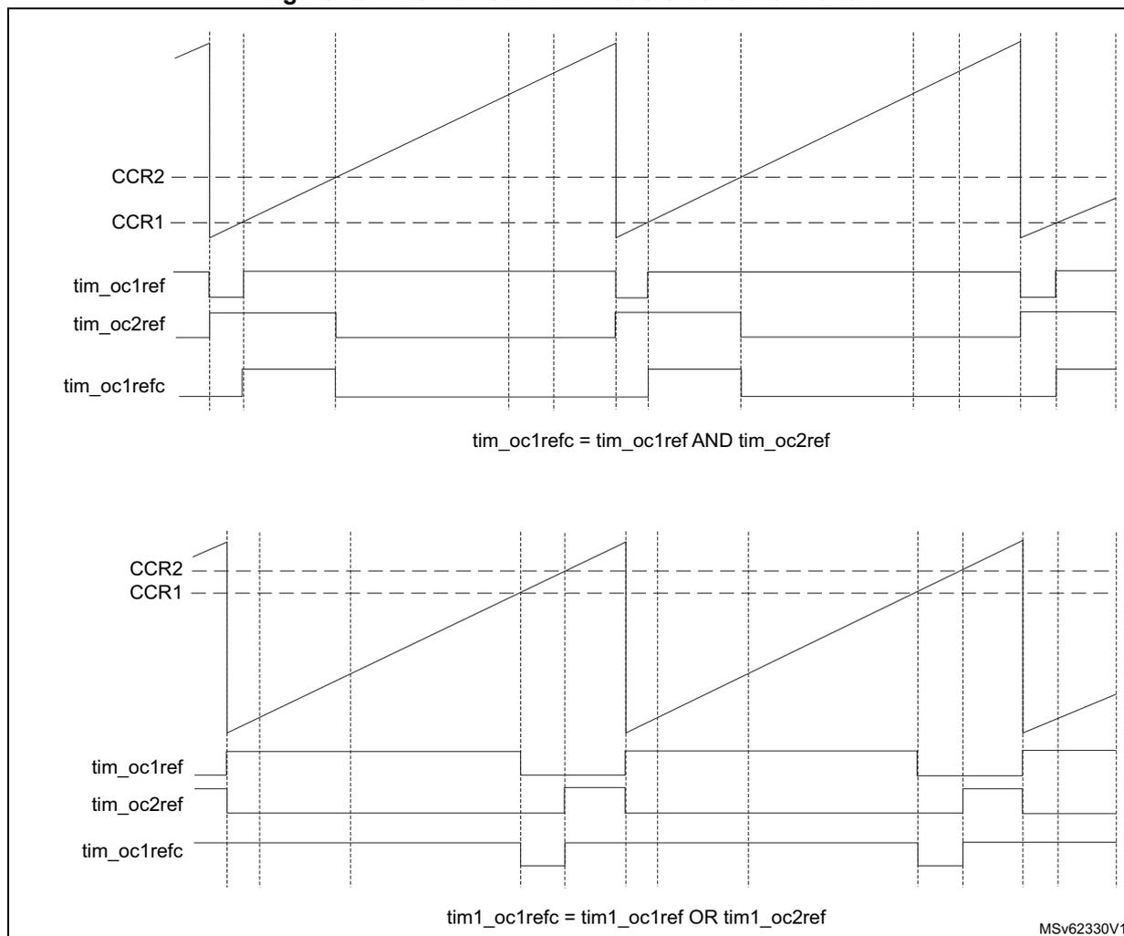
Timing diagram showing combined PWM mode on channel 1 and 2. The top diagram illustrates the AND combination of \( tim\_oc1ref \) and \( tim\_oc2ref \) to produce \( tim\_oc1refc \) . The bottom diagram illustrates the OR combination of \( tim1\_oc1ref \) and \( tim1\_oc2ref \) to produce \( tim1\_oc1refc \) . Both diagrams show the relationship between the capture/compare registers (CCR2, CCR1) and the output signals over time.
Top diagram: \( tim\_oc1refc = tim\_oc1ref \text{ AND } tim\_oc2ref \)
Bottom diagram: \( tim1\_oc1refc = tim1\_oc1ref \text{ OR } tim1\_oc2ref \)
MSv62330V1
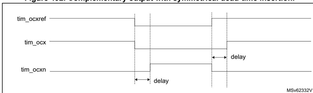
31.4.14 Complementary outputs and dead-time insertion
The TIM15/TIM16/TIM17 general-purpose timers can output one complementary signal and manage the switching-off and switching-on of the outputs.
This time is generally known as dead-time and it has to be adjusted depending on the devices that are connected to the outputs and their characteristics (such as intrinsic delays of level-shifters and delays due to power switches)
The polarity of the outputs (main output \( tim\_ocx \) or complementary \( tim\_ocxn \) ) can be selected independently for each output. This is done by writing to the \( CCxP \) and \( CCxNP \) bits in the \( TIMx\_CCER \) register.
The complementary signals \( tim\_ocx \) and \( tim\_ocxn \) are activated by a combination of several control bits: the \( CCxE \) and \( CCxNE \) bits in the \( TIMx\_CCER \) register and the \( MOE \) , \( OISx \) , \( OISxN \) , \( OSSI \) and \( OSSR \) bits in the \( TIMx\_BDTR \) and \( TIMx\_CR2 \) registers. Refer to Table 318: Output control bits for complementary \( tim\_oc1 \) and \( tim\_oc1n \) channels with break feature (TIM16/TIM17) for more details. In particular, the dead-time is activated when switching to the idle state ( \( MOE \) falling down to 0).
Dead-time insertion is enabled by setting both CCxE and CCxNE bits, and the MOE bit if the break circuit is present. There is one 10-bit dead-time generator for each channel. From a reference waveform tim_ocxref, it generates two outputs tim_ocx and tim_ocxn. If tim_ocx and tim_ocxn are active high:
- • The tim_ocx output signal is the same as the reference signal except for the rising edge, which is delayed relative to the reference rising edge.
- • The tim_ocxn output signal is the opposite of the reference signal except for the rising edge, which is delayed relative to the reference falling edge.
If the delay is greater than the width of the active output (tim_ocx or tim_ocxn) then the corresponding pulse is not generated.
The following figures show the relationships between the output signals of the dead-time generator and the reference signal tim_ocxref. (in these examples CCxP = 0, CCxNP = 0, MOE = 1, CCxE = 1 and CCxNE = 1)
Figure 492. Complementary output with symmetrical dead-time insertion.
The DTAE bit in the TIMx_DTR2 is used to differentiate the deadtime values for rising and falling edges of the reference signal, as shown on Figure 493 .
In asymmetrical mode (DTAE = 1), the rising edge-referred deadtime is defined by the DTG[7:0] bitfield in the TIMx_BDTR register, while the falling edge-referred is defined by the DTGF[7:0] bitfield in the TIMx_DTR2 register. The DTAE bit must be written before enabling the counter and must not be modified while CEN = 1.
It is possible to have the deadtime value updated on-the-fly during pwm operation, using a preload mechanism. The deadtime bitfield DTG[7:0] and DTGF[7:0] are preloaded when the DTPE bit is set in the TIMx_DTR2 register. The preload value is loaded in the active register on the next update event.
Note: If the DTPE bit is enabled while the counter is enabled, any new value written since last update is discarded and previous value is used.
Figure 493. Asymmetrical deadtime
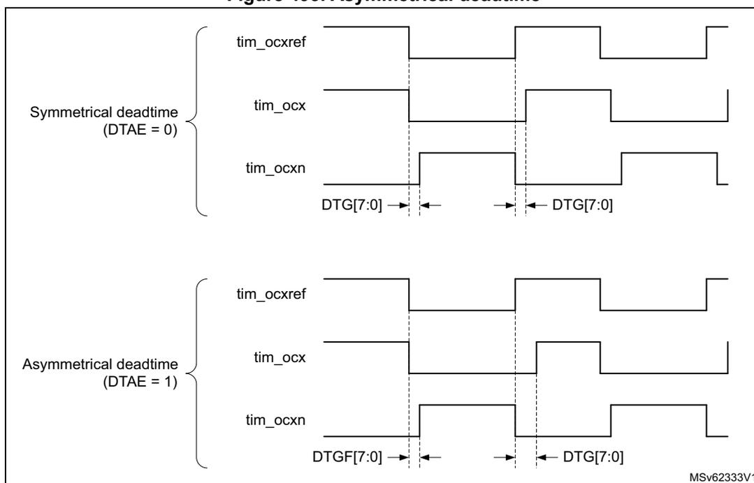
The diagram illustrates two sets of waveforms for tim_ocref , tim_ocx , and tim_ocxn . The top set, labeled Symmetrical deadtime (DTAE = 0) , shows tim_ocx and tim_ocxn signals with deadtime intervals labeled DTG[7:0] . The bottom set, labeled Asymmetrical deadtime (DTAE = 1) , shows the same signals but with different deadtime intervals labeled DTGF[7:0] and DTG[7:0] . The reference signal tim_ocref is a periodic square wave.
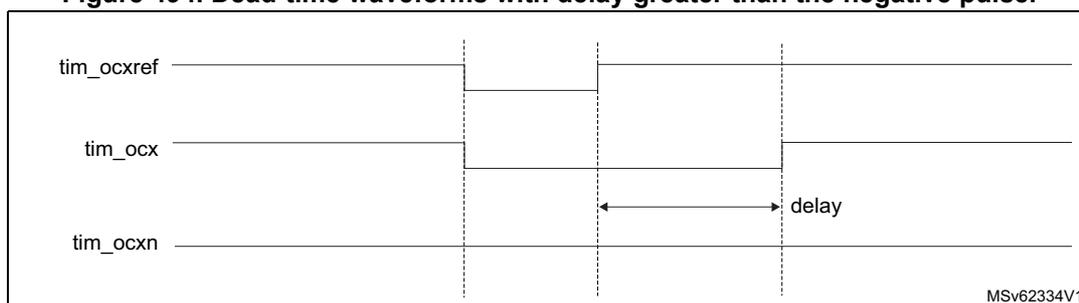
Figure 494. Dead-time waveforms with delay greater than the negative pulse.
The diagram shows the waveforms for tim_ocref , tim_ocx , and tim_ocxn . A horizontal double-headed arrow labeled delay indicates the time interval between the falling edge of tim_ocx and the rising edge of tim_ocxn . This delay is shown to be greater than the duration of the negative pulse of tim_ocx .
Figure 495. Dead-time waveforms with delay greater than the positive pulse.
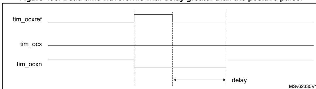
The diagram shows the waveforms for tim_ocref , tim_ocx , and tim_ocxn . A horizontal double-headed arrow labeled delay indicates the time interval between the falling edge of tim_ocx and the rising edge of tim_ocxn . This delay is shown to be greater than the duration of the positive pulse of tim_ocx .
The dead-time delay is the same for each of the channels and is programmable with the DTG bits in the TIMx_BDTR register. Refer to Section 31.8.14: TIMx break and dead-time register (TIMx_BDTR)(x = 16 to 17) for delay calculation.
Redirecting tim_ocxref to tim_ocx or tim_ocxn
In output mode (forced, output compare or PWM), tim_ocxref can be redirected to the tim_ocx output or to tim_ocxn output by configuring the CCxE and CCxNE bits in the TIMx_CCER register.
This is used to send a specific waveform (such as PWM or static active level) on one output while the complementary remains at its inactive level. Other alternative possibilities are to have both outputs at inactive level or both outputs active and complementary with dead-time.
Note: When only tim_ocxn is enabled (CCxE = 0, CCxNE = 1), it is not complemented and becomes active as soon as tim_ocxref is high. For example, if CCxNP = 0 then tim_ocxn = tim_ocxref. On the other hand, when both tim_ocx and tim_ocxn are enabled (CCxE = CCxNE = 1) tim_ocx becomes active when tim_ocxref is high whereas tim_ocxn is complemented and becomes active when tim_ocxref is low.
31.4.15 Using the break function
The purpose of the break function is to protect power switches driven by PWM signals generated with the timers. The break input is usually connected to fault outputs of power stages and 3-phase inverters. When activated, the break circuitry shuts down the PWM outputs and forces them to a predefined safe state.
The break channel gathers both system-level fault (such as clock failure, ECC/parity, and errors) and application fault (from input pins and built-in comparator), and can force the outputs to a predefined level (either active or inactive) after a deadtime duration.
The output enable signal and output levels during break are depending on several control bits:
- • The MOE bit in TIMx_BDTR register is used to enable /disable the outputs by software and is reset in case of break or break2 event.
- • The OSSI bit in the TIMx_BDTR register defines whether the timer controls the output in inactive state or releases the control to the GPIO controller (typically to have it in Hi-Z mode).
- • The OISx and OISxN bits in the TIMx_CR2 register which are setting the output shut-down level, either active or inactive. The tim_ocx and tim_ocxn outputs cannot be set both to active level at a given time, whatever the OISx and OISxN values. Refer to Table 318: Output control bits for complementary tim_oc1 and tim_oc1n channels with break feature (TIM16/TIM17) for more details.
When exiting from reset, the break circuit is disabled and the MOE bit is low. The break function is enabled by setting the BKE bit in the TIMx_BDTR register. The break input polarity can be selected by configuring the BKP bit in the same register. BKE and BKP can be modified at the same time. When the BKE and BKP bits are written, a delay of one APB clock cycle is applied before the writing is effective. Consequently, it is necessary to wait one APB clock period to correctly read back the bit after the write operation.
Because MOE falling edge can be asynchronous, a resynchronization circuit has been inserted between the actual signal (acting on the outputs) and the synchronous control bit (accessed in the TIMx_BDTR register). It results in some delays between the asynchronous and the synchronous signals. In particular, if MOE is set to 1 whereas it was low, a delay must be inserted (dummy instruction) before reading it correctly. This is because the write acts on the asynchronous signal whereas the read reflects the synchronous signal.
The break is generated by the
tim_brk
inputs which have:
- • Programmable polarity (BKP bit in the
TIMx_BDTRregister). - • Programmable enable bit (BKE bit in the
TIMx_BDTRregister). - • Programmable filter (BKF[3:0] bits in the
TIMx_BDTRregister) to avoid spurious events.
The break can be generated from multiple sources which can be individually enabled and with programmable edge sensitivity, using the
TIMx_AF1
register.
The sources for break (
tim_brk
) channel are:
- • External sources connected to one of the
TIM_BKINpins (as per selection done in the GPIO alternate function selection registers), with polarity selection and optional digital filtering. - • Internal sources:
- – Coming from a
tim_brk_cmpxinput (refer to Section 31.4.2: TIM15/TIM16/TIM17 pins and internal signals for product specific implementation). - – Coming from a system break request on the
tim_sys_brkinputs (refer to Section 31.4.2: TIM15/TIM16/TIM17 pins and internal signals for product specific implementation).
- – Coming from a
Break events can also be generated by software using BG bit in the
TIMx_EGR
register. All sources are ORed before entering the timer
tim_brk
inputs, as per
Figure 496
below.
Figure 496. Break circuitry overview
![Figure 496. Break circuitry overview. This logic diagram shows the internal circuitry for generating break signals. At the top, five system break inputs (tim_sys_brk0 to tim_sys_brkx) are each connected to an AND gate along with an 'Enable' signal. The outputs of these AND gates are ORed together to form the 'tim_sys_brk' signal, which triggers the SBIF flag. Below this, external break sources include TIMx_BKIN (from AF controller) through a BKINP input and BKINE gate, and internal break sources (tim_brk_cmp[4:1] and tim_brk_cmp[8:5]) through BKCMP gates (BKCMP1E..BKCMP4E and BKCMP5E..BKCMP8E). These are ORed and then passed through a programmable filter (BKF[3:0]) and a polarity stage (BKP). The filtered signal is ORed with a software break request (BG) via a BKE gate to produce the final 'tim_brk' signal, which triggers the BIF flag. The diagram is labeled MSV62368V2.](/RM0440-STM32G4/710a8fc28c1f740c7e4d40258b21efd6_img.jpg)
Caution: An asynchronous (clockless) operation is only guaranteed when the programmable filter is disabled. If it is enabled, a fail-safe clock mode (for example, using the internal PLL and/or the CSS) must be used to guarantee that break events are handled.
When a break occurs (selected level on the break input):
- • The MOE bit is cleared asynchronously, putting the outputs in inactive state, idle state, or even releasing the control to the GPIO (selected by the OSSI bit). This feature functions even if the MCU oscillator is off.
- • Each output channel is driven with the level programmed in the OISx bit in the TIMx_CR2 register as soon as MOE = 0. If OSSI = 0, the timer releases the output control (taken over by the GPIO) else the enable output remains high.
- • When complementary outputs are used:
- – The outputs are first put in reset state inactive state (depending on the polarity). This is done asynchronously so that it works even if no clock is provided to the timer.
- – If the timer clock is still present, then the dead-time generator is reactivated in order to drive the outputs with the level programmed in the OISx and OISxN bits after a dead-time. Even in this case, tim_ocx and tim_ocxn cannot be driven to their active level together. Note that because of the resynchronization on MOE, the dead-time duration is a bit longer than usual (around 2 tim_ker_ck clock cycles).
- – If OSSI = 0 then the timer releases the enable outputs (taken over by the GPIO which forces a Hi-Z state) else the enable outputs remain or become high as soon as one of the CCxE or CCxNE bits is high.
- • The break status flag (BIF bit in the TIMx_SR register) is set. An interrupt can be generated if the BIE bit in the TIMx_DIER register is set. A DMA request can be sent if the BDE bit in the TIMx_DIER register is set.
- • If the AOE bit in the TIMx_BDTR register is set, the MOE bit is automatically set again at the next update event UEV. This can be used to perform a regulation, for instance. Else, MOE remains low until it is written with 1 again. In this case, it can be used for security and the break input can be connected to an alarm from power drivers, thermal sensors or any security components.
Note: If the MOE is reset by the CPU while the AOE bit is set, the outputs are in idle state and forced to inactive level or Hi-Z depending on OSSI value. If both the MOE and AOE bits are reset by the CPU, the outputs are in disabled state and driven with the level programmed in the OISx bit in the TIMx_CR2 register.
The break inputs are acting on level. Thus, the MOE cannot be set while the break input is active (neither automatically nor by software). In the meantime, the status flag BIF cannot be cleared.
The break can be generated by the tim_brk input which has a programmable polarity and an enable bit BKE in the TIMx_BDTR register.
In addition to the break input and the output management, a write protection has been implemented inside the break circuit to safeguard the application. It is used to freeze the configuration of several parameters (dead-time duration, tim_ocx/tim_ocxn polarities and state when disabled, OCxM configurations, break enable, and polarity). The protection can be selected among 3 levels with the LOCK bits in the TIMx_BDTR register. Refer to Section 31.8.14: TIMx break and dead-time register (TIMx_BDTR)(x = 16 to 17) . The LOCK bits can be written only once after an MCU reset.
The Figure 497 shows an example of behavior for the outputs in response to a break.
Figure 497. Output behavior in response to a break event on tim_brk
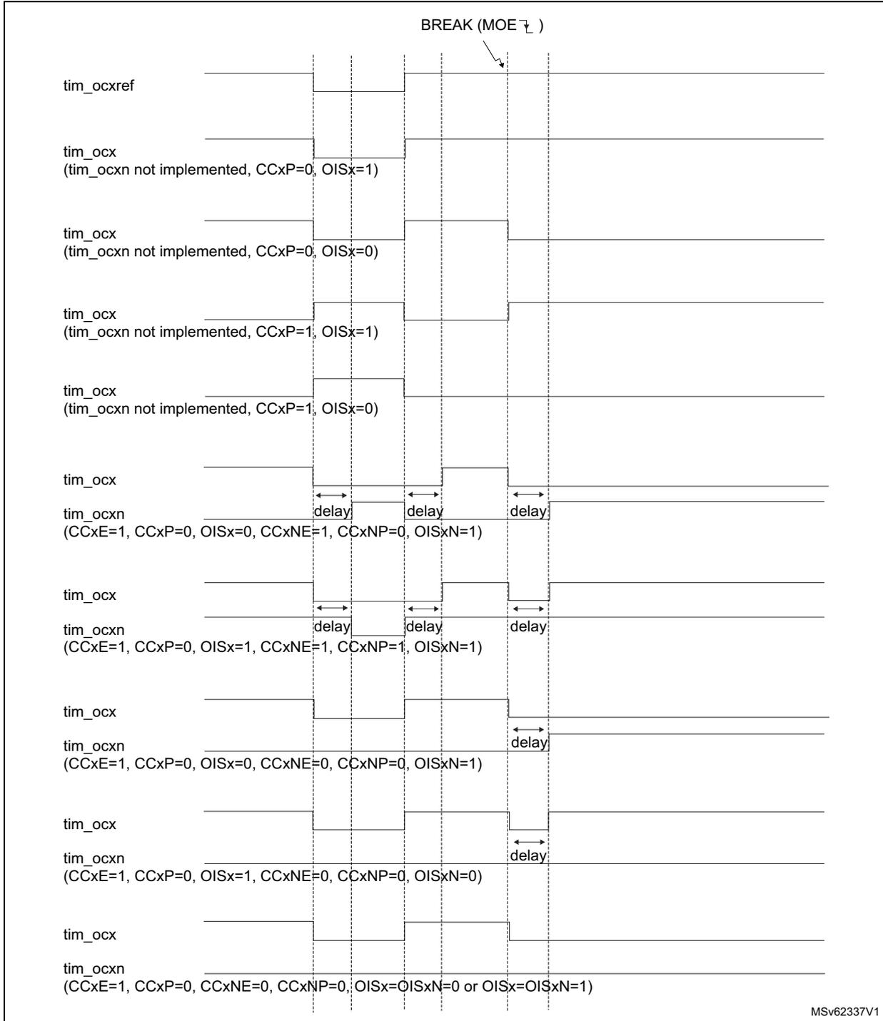
The figure is a timing diagram illustrating the output behavior of a timer in response to a break event. The break event is indicated by a vertical dashed line labeled 'BREAK (MOE ̳ )'. The diagram shows the state of various output pins before and after the break event.
- tim_ocxref : Reference output, shown as a constant high level.
- tim_ocx
: Compare output x. Its state depends on configuration:
- When tim_ocxn is not implemented and CCxP=0, OISx=1 , it is initially high and remains high after the break.
- When tim_ocxn is not implemented and CCxP=0, OISx=0 , it is initially low and remains low after the break.
- When tim_ocxn is not implemented and CCxP=1, OISx=1 , it is initially low and becomes high after the break.
- When tim_ocxn is not implemented and CCxP=1, OISx=0 , it is initially high and becomes low after the break.
- When tim_ocxn is implemented and CCxE=1, CCxP=0, OISx=0, CCxNE=1, CCxNP=0, OISxN=1 , it is initially high and becomes low after a delay following the break.
- When tim_ocxn is implemented and CCxE=1, CCxP=0, OISx=1, CCxNE=1, CCxNP=1, OISxN=1 , it is initially low and becomes high after a delay following the break.
- When tim_ocxn is implemented and CCxE=1, CCxP=0, OISx=0, CCxNE=0, CCxNP=0, OISxN=1 , it is initially high and remains high after the break.
- When tim_ocxn is implemented and CCxE=1, CCxP=0, OISx=1, CCxNE=0, CCxNP=0, OISxN=0 , it is initially low and remains low after the break.
- When tim_ocxn is implemented and CCxE=1, CCxP=0, CCxNE=0, CCxNP=0, OISx=OISxN=0 or OISx=OISxN=1 , it is initially high and becomes low after the break.
- tim_ocxn
: Inverted compare output x. It is only relevant when
CCxE=1
.
- When tim_ocx is not implemented, it is not shown.
- When CCxE=1, CCxP=0, OISx=0, CCxNE=1, CCxNP=0, OISxN=1 , it is initially low and becomes high after a delay following the break.
- When CCxE=1, CCxP=0, OISx=1, CCxNE=1, CCxNP=1, OISxN=1 , it is initially high and becomes low after a delay following the break.
- When CCxE=1, CCxP=0, OISx=0, CCxNE=0, CCxNP=0, OISxN=1 , it is initially low and remains low after the break.
- When CCxE=1, CCxP=0, OISx=1, CCxNE=0, CCxNP=0, OISxN=0 , it is initially high and remains high after the break.
- When CCxE=1, CCxP=0, CCxNE=0, CCxNP=0, OISx=OISxN=0 or OISx=OISxN=1 , it is initially low and becomes high after the break.
Delays are indicated by double-headed arrows labeled 'delay' between the break event and the output state change.
MSv62337V1
31.4.16 Bidirectional break input
The TIM15/TIM16/TIM17 are featuring bidirectional break I/Os, as represented on Figure 498 .
They are used to have:
- • A board-level global break signal available for signaling faults to external MCUs or gate drivers, with a unique pin being both an input and an output status pin.
- • Internal break sources and multiple external open drain sources ORed together to trigger a unique break event, when multiple internal and external break sources must be merged.
The tim_brk input is configured in bidirectional mode using the BKBID bit in the TIMxBDTR register. The BKBID programming bit can be locked in read-only mode using the LOCK bits in the TIMxBDTR register (in LOCK level 1 or above).
The bidirectional mode requires the I/O to be configured in open-drain mode with active low polarity (using BKINP and BKP bits). Any break request coming either from system (for example CSS), from on-chip peripherals, or from break inputs forces a low level on the break input to signal the fault event. The bidirectional mode is inhibited if the polarity bits are not correctly set (active high polarity), for safety purposes.
The break software event (triggered by setting the BG bit) also causes the break I/O to be forced to '0' to indicate to the external components that the timer has entered in break state. However, this is valid only if the break is enabled (BKE = 1). When a software break event is generated with BKE = 0, the outputs are put in safe state and the break flag is set, but there is no effect on the TIM_BKIN I/O.
A safe disarming mechanism prevents the system to be definitively locked-up (a low level on the break input triggers a break which enforces a low level on the same input).
When the BKDSRM bit is set to 1, this releases the break output to clear a fault signal and to give the possibility to re-arm the system.
At no point the break protection circuitry can be disabled:
- • The break input path is always active: a break event is active even if the BKDSRM bit is set and the open drain control is released. This prevents the PWM output to be restarted as long as the break condition is present.
- • The BKDSRM bit cannot disarm the break protection as long as the outputs are enabled (MOE bit is set) (see Table 312 ).
Table 312. Break protection disarming conditions
| MOE | BKBID | BKDSRM | Break protection state |
|---|---|---|---|
| 0 | 0 | X | Armed |
| 0 | 1 | 0 | Armed |
| 0 | 1 | 1 | Disarmed |
| 1 | X | X | Armed |
Arming and rearming break circuitry
The break circuitry (in input or bidirectional mode) is armed by default (peripheral reset configuration).
The following procedure must be followed to re-arm the protection after a break event:
- • The BKDSRM bit must be set to release the output control.
- • The software must wait until the system break condition disappears (if any) and clear the SBIF status flag (or clear it systematically before rearming).
- • The software must poll the BKDSRM bit until it is cleared by hardware (when the application break condition disappears).
From this point, the break circuitry is armed and active, and the MOE bit can be set to re-enable the PWM outputs.
Figure 498. Output redirection
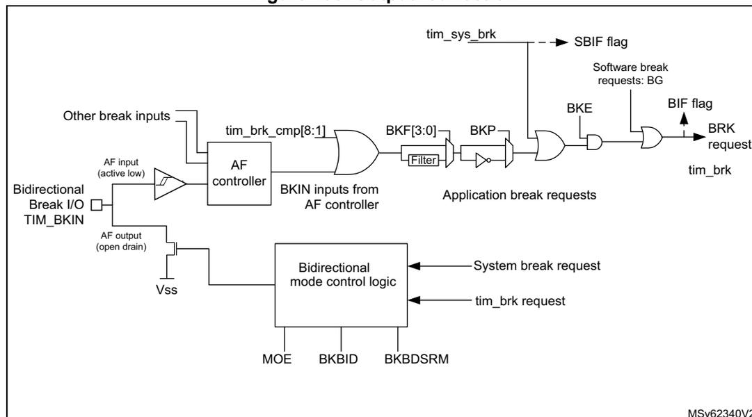
The diagram illustrates the internal logic for break signal handling. On the left, 'Other break inputs' and a 'Bidirectional Break I/O TIM_BKIN' (with 'AF input (active low)' and 'AF output (open drain)' connected to 'Vss') are inputs to an 'AF controller'. The 'AF controller' outputs 'tim_brk_cmp[8:1]' and 'BKIN inputs from AF controller'. These are combined in an AND gate. The output of the AND gate passes through a 'Filter' block labeled 'BKF[3:0]' and then through an inverter labeled 'BKP'. The output of the inverter is combined with 'Application break requests' in an OR gate. The output of this OR gate is labeled 'tim_sys_brk' and is connected to the 'SBIF flag'. This same signal also passes through a 'BKE' (Break Enable) input of another OR gate. The second OR gate also receives 'Software break requests: BG' and its output is labeled 'BIF flag' and 'BRK request' and 'tim_brk'. Below the main logic, a 'Bidirectional mode control logic' block receives 'System break request' and 'tim_brk request' inputs. It has three output pins: 'MOE', 'BKBID', and 'BKDSRM'.
31.4.17 Clearing the tim_ocxref signal on an external event
The tim_ocxref signal of a given channel can be cleared when a high level is applied on the tim_ocref_clr_int input (OCxCE enable bit in the corresponding TIMx_CCMRx register set to 1). tim_ocxref remains low until the next transition to the active state, on the following PWM cycle. This function can only be used in Output compare and PWM modes. It does not work in Forced mode.
The tim_ocref_clr_int input can be selected among several inputs, as shown on Figure 509 below.
Figure 499. tim_ocref_clr input selection multiplexer
![Diagram of the tim_ocref_clr input selection multiplexer. It shows a multiplexer block with eight inputs labeled tim_ocref_clr0 through tim_ocref_clr7. The selection is controlled by a register TIMx_AF2 containing the OCRSEL[2:0] bits. The output of the multiplexer is labeled tim_ocref_clr_int. The diagram is labeled MSv62369V1 in the bottom right corner.](/RM0440-STM32G4/929b9a873a577e4fae8161ee6245112a_img.jpg)
The diagram illustrates a multiplexer for selecting the tim_ocref_clr input. At the top, a box labeled TIMx_AF2 contains the OCRSEL[2:0] selection bits. Below this, a vertical stack of eight inputs is labeled tim_ocref_clr0, tim_ocref_clr1, tim_ocref_clr2, tim_ocref_clr3, tim_ocref_clr4, tim_ocref_clr5, tim_ocref_clr6, and tim_ocref_clr7. These inputs are connected to a trapezoidal multiplexer symbol. The output of the multiplexer is a single line labeled tim_ocref_clr_int. In the bottom right corner of the diagram area, the text MSv62369V1 is present.
31.4.18 6-step PWM generation
When complementary outputs are used on a channel, preload bits are available on the OCxM, CCxE, and CCxNE bits. The preload bits are transferred to the shadow bits at the COM commutation event. Thus one can program in advance the configuration for the next step and change the configuration of all the channels at the same time. COM can be generated by software by setting the COM bit in the TIMx_EGR register or by hardware (on tim_trgi rising edge).
A flag is set when the COM event occurs (COMIF bit in the TIMx_SR register), which can generate an interrupt (if the COMIE bit is set in the TIMx_DIER register) or a DMA request (if the COMDE bit is set in the TIMx_DIER register).
The Figure 500 describes the behavior of the tim_ocx and tim_ocxn outputs when a COM event occurs, in 3 different examples of programmed configurations.
Figure 500. 6-step generation, COM example (OSSR = 1)
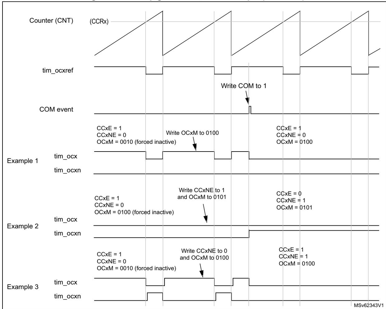
The figure is a timing diagram illustrating the 6-step generation using the COM (Capture/Compare Output Management) feature of a general-purpose timer (TIM15/TIM16/TIM17) with OSSR = 1. The diagram shows the relationship between the Counter (CNT), the timer output reference (tim_ocxref), the COM event, and three examples of timer output signals (tim_ocx and tim_ocxn) under different configuration settings.
- Counter (CNT) (CCRx): The counter is shown as a sawtooth wave, indicating it is running and comparing against the CCRx register level.
- tim_ocxref: The timer output reference signal is shown as a pulse-width modulated signal, which is the reference for the output signals.
- COM event: A pulse is shown on the COM event line, triggered by a "Write COM to 1". This event updates the shadow registers.
- Example 1: Shows a transition where CCxE = 1 , CCxNE = 0 , and OCxM = 0010 (forced inactive) . A "Write OCxM to 0100" occurs. After the COM event, the configuration becomes CCxE = 1 , CCxNE = 0 , and OCxM = 0100 , causing tim_ocx to start toggling based on tim_ocxref .
- Example 2: Shows a transition where CCxE = 1 , CCxNE = 0 , and OCxM = 0100 (forced inactive) . A "Write CCxNE to 1 and OCxM to 0101" occurs. After the COM event, the configuration becomes CCxE = 0 , CCxNE = 1 , and OCxM = 0101 , causing tim_ocxn to become active.
- Example 3: Shows a transition where CCxE = 1 , CCxNE = 0 , and OCxM = 0010 (forced inactive) . A "Write CCxNE to 0 and OCxM to 0100" occurs. After the COM event, the configuration becomes CCxE = 1 , CCxNE = 1 , and OCxM = 0100 , causing both tim_ocx and tim_ocxn to toggle.
MSv62343V1
31.4.19 One-pulse mode
One-pulse mode (OPM) is a particular case of the previous modes. It allows the counter to be started in response to a stimulus and to generate a pulse with a programmable length after a programmable delay.
Starting the counter can be controlled through the slave mode controller. Generating the waveform can be done in output compare mode or PWM mode. One-pulse mode is selected by setting the OPM bit in the TIMx_CR1 register. This makes the counter stop automatically at the next update event UEV.
A pulse can be correctly generated only if the compare value is different from the counter initial value. Before starting (when the timer is waiting for the trigger), the configuration must be:
- • \( CNT < CCRx \leq ARR \) (in particular, \( 0 < CCRx \) ).
Figure 501. Example of one pulse mode.
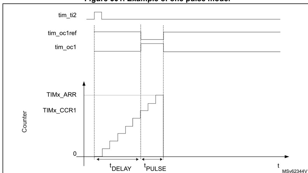
For example one may want to generate a positive pulse on tim_oc1 with a length of \( t_{PULSE} \) and after a delay of \( t_{DELAY} \) as soon as a positive edge is detected on the tim_ti2 input pin.
Let's use tim_ti2fp2 as trigger 1:
- 1. Select the proper tim_ti2_in[15:1] source (internal or external) with the TI2SEL[3:0] bits in the TIMx_TISEL register.
- 2. Map tim_ti2fp2 to tim_ti2 by writing CC2S = 01 in the TIMx_CCMR1 register.
- 3. tim_ti2fp2 must detect a rising edge, write CC2P = 0 and CC2NP = 0 in the TIMx_CCER register.
- 4. Configure tim_ti2fp2 as trigger for the slave mode controller (tim_trgi) by writing TS = 00110 in the TIMx_SMCR register.
- 5. tim_ti2fp2 is used to start the counter by writing SMS to 110 in the TIMx_SMCR register (trigger mode).
The OPM waveform is defined by writing the compare registers (taking into account the clock frequency and the counter prescaler).
- • The \( t_{\text{DELAY}} \) is defined by the value written in the TIMx_CCR1 register.
- • The \( t_{\text{PULSE}} \) is defined by the difference between the autoreload value and the compare value (TIMx_ARR - TIMx_CCR1).
- • Let's say one wants to build a waveform with a transition from 0 to 1 when a compare match occurs and a transition from 1 to 0 when the counter reaches the autoreload value. To do this PWM mode 2 must be enabled by writing OC1M = 111 in the TIMx_CCMR1 register. Optionally the preload registers can be enabled by writing OC1PE = 1 in the TIMx_CCMR1 register and ARPE in the TIMx_CR1 register. In this case one has to write the compare value in the TIMx_CCR1 register, the autoreload value in the TIMx_ARR register, generate an update by setting the UG bit and wait for external trigger event on tim_ti2. CC1P is written to 0 in this example.
Since only one pulse is needed, a 1 must be written in the OPM bit in the TIMx_CR1 register to stop the counter at the next update event (when the counter rolls over from the autoreload value back to 0).
Particular case: tim_ocx fast enable
In One-pulse mode, the edge detection on tim_tix input set the CEN bit which enables the counter. Then the comparison between the counter and the compare value makes the output toggle. But several clock cycles are needed for these operations and it limits the minimum delay \( t_{\text{DELAY}} \) min that can be obtained.
If one wants to output a waveform with the minimum delay, the OCxFE bit can be set in the TIMx_CCMRx register. Then tim_ocxref (and tim_ocx) are forced in response to the stimulus, without taking in account the comparison. Its new level is the same as if a compare match had occurred. OCxFE acts only if the channel is configured in PWM1 or PWM2 mode.
31.4.20 Retriggerable one pulse mode (TIM15 only)
This mode allows the counter to be started in response to a stimulus and to generate a pulse with a programmable length, but with the following differences with non-retriggerable one pulse mode described in Section 31.4.19 :
- • The pulse starts as soon as the trigger occurs (no programmable delay)
- • The pulse is extended if a new trigger occurs before the previous one is completed
The timer must be in Slave mode, with the bits SMS[3:0] = 1000 (Combined reset + trigger mode) in the TIMx_SMCR register, and the OCxM[3:0] bits set to 1000 or 1001 for Retriggerable OPM mode 1 or 2.
If the timer is configured in Up-counting mode, the corresponding CCRx must be set to 0 (the ARR register sets the pulse length). If the timer is configured in Down-counting mode, CCRx must be above or equal to ARR.
Note: The OCxM[3:0] and SMS[3:0] bit fields are split into two parts for compatibility reasons, the most significant bit are not contiguous with the three least significant ones.
This mode must not be used with center-aligned PWM modes. It is mandatory to have CMS[1:0] = 00 in TIMx_CR1.
Figure 502. Retriggerable one pulse mode
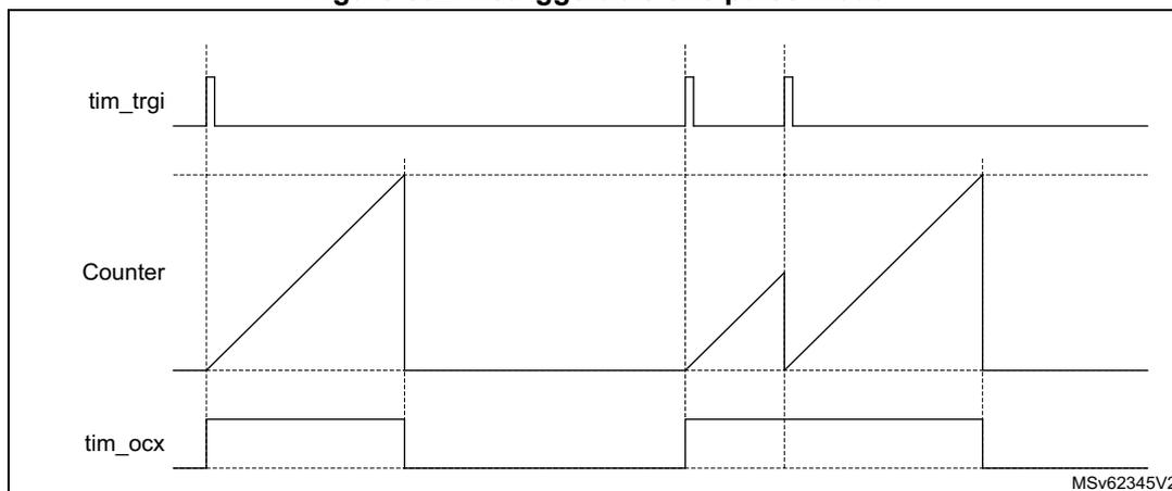
The diagram illustrates the retriggerable one pulse mode. The top signal, tim_trgi , shows three trigger pulses. The middle signal, Counter , is a sawtooth wave that increments when tim_trgi is high and resets to zero when tim_trgi goes low. The bottom signal, tim_ocx , is a rectangular pulse that goes high when the counter starts and low when the counter reaches the auto-reload value. The counter is retriggered by the second pulse of tim_trgi before it reaches the auto-reload value, causing it to reset and start again. The third pulse of tim_trgi retriggeres the counter again. The counter value is shown as a series of diagonal lines, indicating it is counting up from zero to the auto-reload value.
31.4.21 UIF bit remapping
The IUFREMAP bit in the TIMx_CR1 register forces a continuous copy of the update interrupt flag UIF into bit 31 of the timer counter register (TIMxCNT[31]). This is used to atomically read both the counter value and a potential roll-over condition signaled by the UIFCPY flag. In particular cases, it can ease the calculations by avoiding race conditions caused for instance by a processing shared between a background task (counter reading) and an interrupt (update interrupt).
There is no latency between the assertions of the UIF and UIFCPY flags.
31.4.22 Timer input XOR function (TIM15 only)
The TI1S bit in the TIMx_CR2 register, allows the input filter of channel 1 to be connected to the output of a XOR gate, combining the two input pins tim_ti1 and tim_ti2.
The XOR output can be used with all the timer input functions such as trigger or input capture. It is useful for measuring the interval between the edges on two input signals, as shown in Figure 503.
Figure 503. Measuring time interval between edges on 2 signals
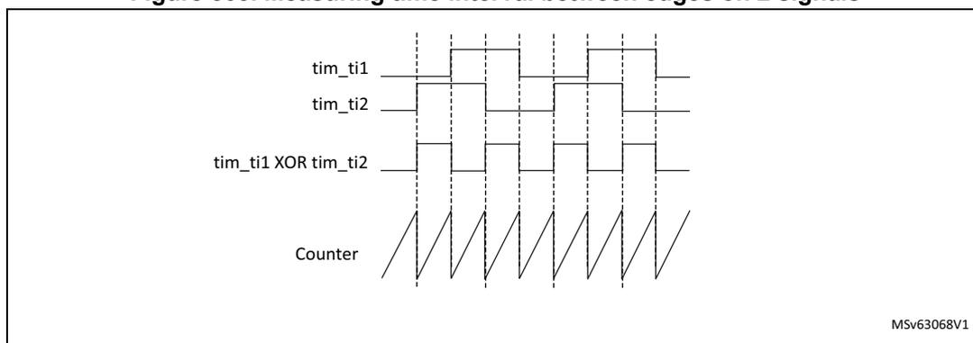
The diagram illustrates the use of the XOR function for measuring time intervals. The top two signals, tim_ti1 and tim_ti2 , are square waves. The third signal, tim_ti1 XOR tim_ti2 , is the output of an XOR gate combining the two input signals. The bottom signal, Counter , is a sawtooth wave that starts at the rising edge of the XOR output and resets at the falling edge. The counter value is shown as a series of diagonal lines, indicating it is counting up from zero to the auto-reload value. The time interval between the rising and falling edges of the XOR output is measured by the counter.
31.4.23 External trigger synchronization (TIM15 only)
The TIM timers are linked together internally for timer synchronization or chaining.
The TIM15 timer can be synchronized with an external trigger in several modes: Reset mode, Gated mode, Trigger mode, Reset + trigger, and gated + reset modes.
Slave mode: Reset mode
The counter and its prescaler can be reinitialized in response to an event on a trigger input. Moreover, if the URS bit from the TIMx_CR1 register is low, an update event UEV is generated. Then all the preloaded registers (TIMx_ARR, TIMx_CCRx) are updated.
In the following example, the upcounter is cleared in response to a rising edge on tim_ti1 input:
- 1. Configure the channel 1 to detect rising edges on tim_ti1. Configure the input filter duration (in this example, no need for any filter, so IC1F is kept at 0000). The capture prescaler is not used for triggering, so it does not need to be configured. The CC1S bits select the input capture source only, CC1S = 01 in the TIMx_CCMR1 register. Write CC1P = 0 and CC1NP = 0 in the TIMx_CCER register to validate the polarity (and detect rising edges only).
- 2. Configure the timer in reset mode by writing SMS = 100 in TIMx_SMCR register. Select tim_ti1 as the input source by writing TS = 00101 in TIMx_SMCR register.
- 3. Start the counter by writing CEN = 1 in the TIMx_CR1 register.
The counter starts counting on the internal clock, then behaves normally until tim_ti1 rising edge. When tim_ti1 rises, the counter is cleared and restarts from 0. In the meantime, the trigger flag is set (TIF bit in the TIMx_SR register) and an interrupt request, or a DMA request can be sent if enabled (depending on the TIE and TDE bits in TIMx_DIER register).
The following figure shows this behavior when the autoreload register TIMx_ARR = 0x36. The delay between the rising edge on tim_ti1 and the actual reset of the counter is due to the resynchronization circuit on tim_ti1 input.
Figure 504. Control circuit in reset mode
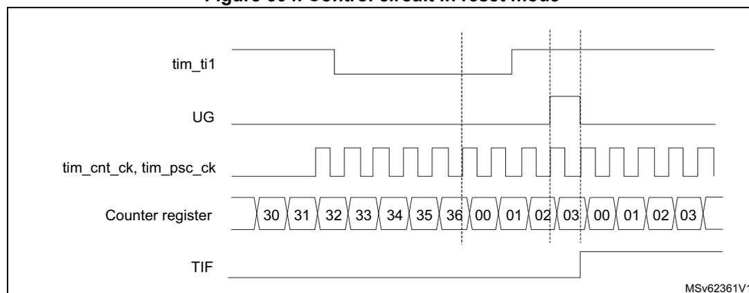
The timing diagram shows the following signals and their relationship:
- tim_ti1 : The external trigger input. It shows a rising edge that initiates the reset sequence.
- UG : Update Generation signal. It pulses high when the counter reaches the autoreload value (0x36) and is reset to low when the counter is cleared.
- tim_cnt_ck, tim_psc_ck : The counter and prescaler clock. It is a periodic square wave.
- Counter register : Shows the count values. It starts at 00, increments to 36, then rolls over to 00. When a rising edge occurs on tim_ti1, the counter is reset to 00. The sequence of values shown is: 30, 31, 32, 33, 34, 35, 36, 00, 01, 02, 03, 00, 01, 02, 03.
- TIF : Trigger Interrupt Flag. It is set (goes high) when a valid rising edge is detected on tim_ti1 and is cleared when the UG signal goes high.
The diagram illustrates that the counter is reset to 00 upon a rising edge on tim_ti1, and the TIF flag is set until the next update event (UG goes high).
MSv62361V1
The counter can be enabled depending on the level of a selected input.
In the following example, the upcounter counts only when tim_ti1 input is low:
- 1. Configure the channel 1 to detect low levels on tim_ti1. Configure the input filter duration (in this example, no need for any filter, so IC1F is kept at 0000). The capture prescaler is not used for triggering, so it does not need to be configured. The CC1S bits select the input capture source only, CC1S = 01 in TIMx_CCMR1 register. Write CC1P = 1 and CC1NP = 0 in the TIMx_CCER register to validate the polarity (and detect low level only).
- 2. Configure the timer in gated mode by writing SMS = 101 in TIMx_SMCR register. Select tim_ti1 as the input source by writing TS = 00101 in TIMx_SMCR register.
- 3. Enable the counter by writing CEN = 1 in the TIMx_CR1 register (in gated mode, the counter does not start if CEN = 0, whatever is the trigger input level).
The counter starts counting on the internal clock as long as tim_ti1 is low and stops as soon as tim_ti1 becomes high. The TIF flag in the TIMx_SR register is set both when the counter starts or stops.
The delay between the rising edge on tim_ti1 and the actual stop of the counter is due to the resynchronization circuit on tim_ti1 input.
Figure 505. Control circuit in gated mode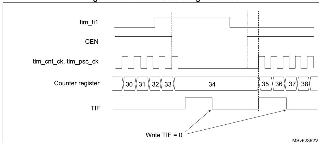
MSV62362V1
Slave mode: Trigger mode
The counter can start in response to an event on a selected input.
In the following example, the upcounter starts in response to a rising edge on tim_ti2 input:
- 1. Configure the channel 2 to detect rising edges on tim_ti2. Configure the input filter duration (in this example, no need for any filter, so IC2F is kept at 0000). The capture prescaler is not used for triggering, so it does not need to be configured. The CC2S bits are configured to select the input capture source only, CC2S = 01 in TIMx_CCMR1 register. Write CC2P = 1 and CC2NP = 0 in the TIMx_CCER register to validate the polarity (and detect low level only).
- 2. Configure the timer in trigger mode by writing SMS = 110 in the TIMx_SMCR register. Select tim_ti2 as the input source by writing TS = 00110 in the TIMx_SMCR register.
When a rising edge occurs on tim_ti2, the counter starts counting on the internal clock and the TIF flag is set.
The delay between the rising edge on tim_ti2 and the actual start of the counter is due to the resynchronization circuit on tim_ti2 input.
Figure 506. Control circuit in trigger mode
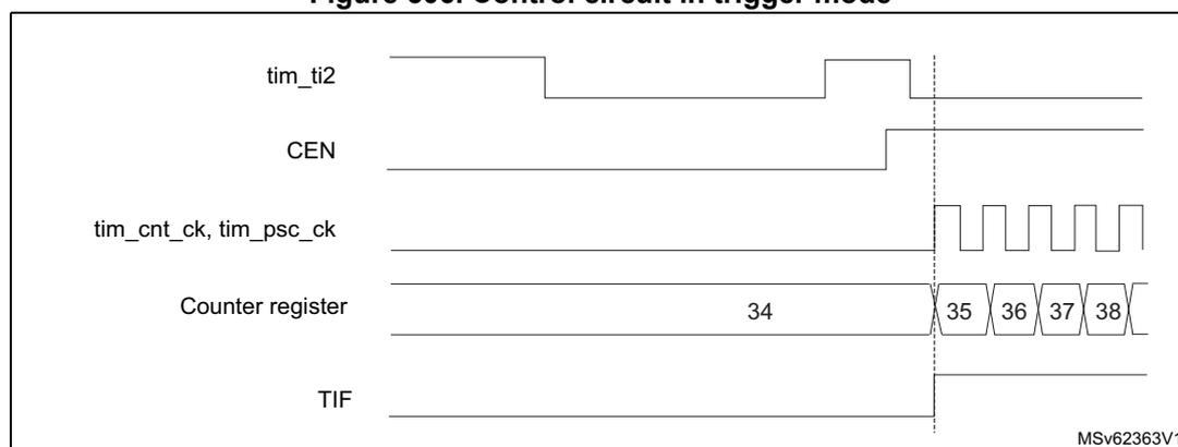
The diagram illustrates the timing relationship between the trigger input (tim_ti2), counter enable (CEN), clock signals (tim_cnt_ck, tim_psc_ck), the counter register value, and the trigger interrupt flag (TIF). A vertical dashed line indicates the rising edge of tim_ti2. Before the edge, tim_ti2 is low, CEN is low, clocks are stopped, and the counter register holds the value 34. At the rising edge, tim_ti2 goes high, which causes CEN to go high, the clocks to start, the counter register to increment to 35, and the TIF flag to go high. The counter then continues to increment (36, 37, 38) as long as tim_ti2 remains high and CEN is high.
Slave mode selection preload for run-time update
The SMS[3:0] bit can be preloaded. This is enabled by setting the SMSPE enable bit in the TIMx_SMCR register. The trigger for the transfer from SMS[3:0] preload to active value is the update event (UEV) occurring when the counter overflows.
31.4.24 Slave mode – combined reset + trigger mode (TIM15 only)
In this case, a rising edge of the selected trigger input (tim_trgi) reinitializes the counter, generates an update of the registers, and starts the counter.
This mode is used for one-pulse mode.
31.4.25 Slave mode – combined reset + gated mode (TIM15 only)
The counter clock is enabled when the trigger input (tim_trgi) is high. The counter stops and (is reset) as soon as the trigger becomes low. Both start and stop of the counter are controlled.
This mode is used to detect out-of-range PWM signal (duty cycle exceeding a maximum expected value).
31.4.26 Timer synchronization (TIM15 only)
The TIMx timers are linked together internally for timer synchronization or chaining. Refer to Section 30.4.23: Timer synchronization for details.
Note: The clock of the slave peripherals (such as timer and ADC) receiving the tim_trgo signal must be enabled prior to receive events from the master timer, and the clock frequency (prescaler) must not be changed on-the-fly while triggers are received from the master timer.
31.4.27 Using timer output as trigger for other timers (TIM16/TIM17 only)
The timers with one channel only do not feature a master mode. However, the OC1 output signal can be used to trigger some other timers (including timers described in other sections of this document). Check the “TIMx internal trigger connection” table of any timer on the device to identify which timers can be targeted as slave.
The OC1 signal pulse width must be programmed to be at least two clock cycles of the destination timer, to make sure the slave timer detects the trigger.
For instance, if the destination's timer CK_INT clock is four times slower than the source timer, the OC1 pulse width must be eight clock cycles.
31.4.28 ADC triggers (TIM15 only)
The timer can generate an ADC triggering event with various internal signals, such as reset, enable or compare events.
Note: The clock of the slave peripherals (such as timer, ADC) receiving the tim_trgo signal must be enabled prior to receive events from the master timer, and the clock frequency (prescaler) must not be changed on-the-fly while triggers are received from the master timer.
31.4.29 DMA burst mode
The TIMx timers have the capability to generate multiple DMA requests on a single event. The main purpose is to be able to reprogram several timer registers multiple times without software overhead, but it can also be used to read several registers in a row, at regular intervals.
The DMA controller destination is unique and must point to the virtual register TIMx_DMAR. On a given timer event, the timer launches a sequence of DMA requests (burst). Each write into the TIMx_DMAR register is actually redirected to one of the timer registers.
The DBL[4:0] bits in the TIMx_DCR register set the DMA burst length. The timer recognizes a burst transfer when a read or a write access is done to the TIMx_DMAR address), i.e. the number of transfers (either in half-words or in bytes).
The DBA[4:0] bits in the TIMx_DCR registers define the DMA base address for DMA transfers (when read/write accesses are done through the TIMx_DMAR address). DBA is defined as an offset starting from the address of the TIMx_CR1 register.
Example:
00000: TIMx_CR1
00001: TIMx_CR2
00010: TIMx_SMCR
For example, the timer DMA burst feature can be used to update the contents of the CCRx registers (x = 2, 3, 4) on an update event, with the DMA transferring half words into the CCRx registers.
This is done in the following steps:
- 1. Configure the corresponding DMA channel as follows:
- – DMA channel peripheral address is the DMAR register address
- – DMA channel memory address is the address of the buffer in the RAM containing the data to be transferred by DMA into the CCRx registers.
- – Number of data to transfer = 3 (See note below).
- – Circular mode disabled.
- 2. Configure the DCR register by configuring the DBA and DBL bit fields as follows: DBL = 3 transfers, DBA = 0xE.
- 3. Enable the TIMx update DMA request (set the UDE bit in the DIER register).
- 4. Enable TIMx
- 5. Enable the DMA channel
This example is for the case where every CCRx register is to be updated once. If every CCRx register is to be updated twice for example, the number of data to transfer must be 6. Let's take the example of a buffer in the RAM containing data1, data2, data3, data4, data5, and data6. The data is transferred to the CCRx registers as follows: on the first update DMA request, data1 is transferred to CCR2, data2 is transferred to CCR3, data3 is transferred to CCR4 and on the second update DMA request, data4 is transferred to CCR2, data5 is transferred to CCR3, and data6 is transferred to CCR4.
Note: A null value can be written to the reserved registers.
31.4.30 TIM15/TIM16/TIM17 DMA requests
The TIM15/TIM16/TIM17 can generate a DMA request, as shown in Table 313 .
Table 313. DMA request
| DMA request signal | DMA acronym | DMA request | Enable control bit |
|---|---|---|---|
| tim_upd_dma | TIM_UP | Update | UDE |
| tim_cc1_dma | TIM_CH1 | Capture/compare 1 | CC1DE |
| tim_com_dma (1) | TIM_COM | Commutation (COM) | COMDE |
| tim_trgi_dma (1) | TIM_TRIG | Trigger | TDE |
- 1. Available for TIM15 only.
31.4.31 Debug mode
When the microcontroller enters debug mode (Cortex ® -M4 with FPU core halted), the TIMx counter can either continue to work normally or stop.
The behavior in debug mode can be programmed with a dedicated configuration bit per timer in the Debug support (DBG) module.
For safety purposes, when the counter is stopped, the outputs are disabled (as if the MOE bit was reset). The outputs can either be forced to an inactive state (OSSI bit = 1), or have their control taken over by the GPIO controller (OSSI bit = 0) to force them to Hi-Z.
For more details, refer to the debug section.
31.5 TIM15/TIM16/TIM17 low-power modes
Table 314. Effect of low-power modes on TIM15/TIM16/TIM17
| Mode | Description |
|---|---|
| Sleep | No effect, peripheral is active. The interrupts can cause the device to exit from Sleep mode. |
| Stop | The timer operation is stopped and the register content is kept. No interrupt can be generated. |
| Standby | The timer is powered-down and must be reinitialized after exiting the Standby mode. |
31.6 TIM15/TIM16/TIM17 interrupts
The TIM15/TIM16/TIM17 can generate multiple interrupts, as shown in Table 315 .
Table 315. Interrupt requests
| Interrupt acronym | Interrupt event | Event flag | Enable control bit | Interrupt clear method | Exit from Sleep mode | Exit from Stop and Standby mode |
|---|---|---|---|---|---|---|
| TIM | Update | UIF | UIE | write 0 in UIF | Yes | No |
| Capture/compare 1 | CC1IF | CC1IE | write 0 in CC1IF | Yes | No | |
| Capture/compare 2 (1) | CC2IF | CC2IE | write 0 in CC2IF | Yes | No | |
| Commutation (COM) | COMIF | COMIE | write 0 in COMIF | Yes | No | |
| Trigger (1) | TIF | TIE | write 0 in TIF | Yes | No | |
| Break | BIF | BIE | write 0 in BIF | Yes | No |
1. Available for TIM15 only.
31.7 TIM15 registers
Refer to Section 1.2 for a list of abbreviations used in register descriptions.
The peripheral registers can be accessed by half-words (16-bit) or words (32-bit).
31.7.1 TIM15 control register 1 (TIM15_CR1)
Address offset: 0x00
Reset value: 0x0000
| 15 | 14 | 13 | 12 | 11 | 10 | 9 | 8 | 7 | 6 | 5 | 4 | 3 | 2 | 1 | 0 |
|---|---|---|---|---|---|---|---|---|---|---|---|---|---|---|---|
| Res. | Res. | Res. | DITH EN | UIFRE MAP | Res. | CKD[1:0] | ARPE | Res. | Res. | Res. | OPM | URS | UDIS | CEN | |
| rw | rw | rw | rw | rw | rw | rw | rw | ||||||||
Bits 15:13 Reserved, must be kept at reset value.
Bit 12 DITHEN : Dithering enable
0: Dithering disabled
1: Dithering enabled
Note: The DITHEN bit can only be modified when CEN bit is reset.
Bit 11 UIFREMAP : UIF status bit remapping
0: No remapping. UIF status bit is not copied to TIM15_CNT register bit 31.
1: Remapping enabled. UIF status bit is copied to TIM15_CNT register bit 31.
Bit 10 Reserved, must be kept at reset value.
Bits 9:8 CKD[1:0] : Clock division
This bitfield indicates the division ratio between the timer clock (tim_ker_ck) frequency and the dead-time and sampling clock ( \( t_{DTS} \) ) used by the dead-time generators and the digital filters (tim_tix)
00: \( t_{DTS} = t_{tim\_ker\_ck} \)
01: \( t_{DTS} = 2 * t_{tim\_ker\_ck} \)
10: \( t_{DTS} = 4 * t_{tim\_ker\_ck} \)
11: Reserved
Bit 7 ARPE : Auto-reload preload enable
0: TIM15_ARR register is not buffered
1: TIM15_ARR register is buffered
Bits 6:4 Reserved, must be kept at reset value.
Bit 3 OPM : One-pulse mode
0: Counter is not stopped at update event
1: Counter stops counting at the next update event (clearing the bit CEN)
Bit 2 URS : Update request source
This bit is set and cleared by software to select the UEV event sources.
0: Any of the following events generate an update interrupt if enabled. These events can be:
- – Counter overflow/underflow
- – Setting the UG bit
- – Update generation through the slave mode controller
1: Only counter overflow/underflow generates an update interrupt if enabled
Bit 1 UDIS : Update disable
This bit is set and cleared by software to enable/disable UEV event generation.
0: UEV enabled. The Update (UEV) event is generated by one of the following events:
- – Counter overflow/underflow
- – Setting the UG bit
- – Update generation through the slave mode controller
Buffered registers are then loaded with their preload values.
1: UEV disabled. The Update event is not generated, shadow registers keep their value (ARR, PSC, CCRx). However the counter and the prescaler are reinitialized if the UG bit is set or if a hardware reset is received from the slave mode controller.
Bit 0 CEN : Counter enable
0: Counter disabled
1: Counter enabled
Note: External clock and gated mode can work only if the CEN bit has been previously set by software. However trigger mode can set the CEN bit automatically by hardware.
31.7.2 TIM15 control register 2 (TIM15_CR2)
Address offset: 0x04
Reset value: 0x0000
| 15 | 14 | 13 | 12 | 11 | 10 | 9 | 8 | 7 | 6 | 5 | 4 | 3 | 2 | 1 | 0 | |
|---|---|---|---|---|---|---|---|---|---|---|---|---|---|---|---|---|
| Res. | Res. | Res. | Res. | Res. | OIS2 | OIS1N | OIS1 | TI1S | MMS[2:0] | CCDS | CCUS | Res. | CCPC | |||
| rw | rw | rw | rw | rw | rw | rw | rw | rw | rw | |||||||
Bits 15:11 Reserved, must be kept at reset value.
Bit 10 OIS2 : Output idle state 2 (tim_oc2 output)
0: tim_oc2 = 0 when MOE = 0
1: tim_oc2 = 1 when MOE = 0
Note: This bit cannot be modified as long as LOCK level 1, 2 or 3 has been programmed (LOCK bits in the TIM15_BKR register).
Bit 9 OIS1N : Output Idle state 1 (tim_oc1n output)
0: tim_oc1n = 0 after a dead-time when MOE = 0
1: tim_oc1n = 1 after a dead-time when MOE = 0
Note: This bit can not be modified as long as LOCK level 1, 2 or 3 has been programmed (LOCK bits in TIM15_BKR register).
Bit 8 OIS1 : Output Idle state 1 (tim_oc1 output)
0: tim_oc1 = 0 after a dead-time when MOE = 0
1: tim_oc1 = 1 after a dead-time when MOE = 0
Note: This bit can not be modified as long as LOCK level 1, 2 or 3 has been programmed (LOCK bits in TIM15_BKR register).
Bit 7 TI1S : tim_ti1 selection- 0: The tim_ti1_in[15:0] multiplexer output is connected to tim_ti1 input
- 1: The tim_ti1_in[15:0] and tim_ti2_in[15:0] multiplexers output are connected to the tim_ti1 input (XOR combination)
These bits are used to select the information to be sent in master mode to slave timers for synchronization (tim_trgo). The combination is as follows:
- 000: Reset - the UG bit from the TIM15_EGR register is used as trigger output (tim_trgo). If the reset is generated by the trigger input (slave mode controller configured in reset mode) then the signal on tim_trgo is delayed compared to the actual reset.
- 001: Enable - the Counter Enable signal CNT_EN is used as trigger output (tim_trgo). It is useful to start several timers at the same time or to control a window in which a slave timer is enable. The Counter Enable signal is generated by a logic AND between CEN control bit and the trigger input when configured in gated mode. When the Counter Enable signal is controlled by the trigger input, there is a delay on tim_trgo, except if the master/slave mode is selected (see the MSM bit description in TIM15_SMCR register).
- 010: Update - The update event is selected as trigger output (tim_trgo). For instance a master timer can then be used as a prescaler for a slave timer.
- 011: Compare Pulse - The trigger output send a positive pulse when the CC1IF flag is to be set (even if it was already high), as soon as a capture or a compare match occurred (tim_trgo).
- 100: Compare - tim_oc1refc signal is used as trigger output (tim_trgo).
- 101: Compare - tim_oc2refc signal is used as trigger output (tim_trgo).
- 0: CCx DMA request sent when CCx event occurs
- 1: CCx DMA requests sent when update event occurs
- 0: When capture/compare control bits are preloaded (CCPC = 1), they are updated by setting the COMG bit only.
- 1: When capture/compare control bits are preloaded (CCPC = 1), they are updated by setting the COMG bit or when an rising edge occurs on tim_trgi.
Note: This bit acts only on channels that have a complementary output.
Bit 1 Reserved, must be kept at reset value.
Bit 0 CCPC : Capture/compare preloaded control- 0: CCxE, CCxNE and OCxM bits are not preloaded
- 1: CCxE, CCxNE and OCxM bits are preloaded, after having been written, they are updated only when a commutation event (COM) occurs (COMG bit set or rising edge detected on tim_trgi, depending on the CCUS bit).
Note: This bit acts only on channels that have a complementary output.
31.7.3 TIM15 slave mode control register (TIM15_SMCR)
Address offset: 0x08
Reset value: 0x0000 0000
| 31 | 30 | 29 | 28 | 27 | 26 | 25 | 24 | 23 | 22 | 21 | 20 | 19 | 18 | 17 | 16 |
|---|---|---|---|---|---|---|---|---|---|---|---|---|---|---|---|
| Res. | Res. | Res. | Res. | Res. | Res. | Res. | SMSPE | Res. | Res. | TS[4:3] | Res. | Res. | Res. | SMS[3] | |
| rw | rw | rw | rw | ||||||||||||
| 15 | 14 | 13 | 12 | 11 | 10 | 9 | 8 | 7 | 6 | 5 | 4 | 3 | 2 | 1 | 0 |
| Res. | Res. | Res. | Res. | Res. | Res. | Res. | Res. | MSM | TS[2:0] | Res. | SMS[2:0] | ||||
| rw | rw | rw | rw | rw | rw | rw | |||||||||
Bits 31:25 Reserved, must be kept at reset value.
Bit 24 SMSPE : SMS preload enable
This bit selects whether the SMS[3:0] bitfield is preloaded.
0: SMS[3:0] bitfield is not preloaded
1: SMS[3:0] preload is enabled
Bits 23:22 Reserved, must be kept at reset value.
Bits 19:17 Reserved, must be kept at reset value.
Bits 15:8 Reserved, must be kept at reset value.
Bit 7 MSM : Master/slave mode
0: No action
1: The effect of an event on the trigger input (tim_trgi) is delayed to allow a perfect synchronization between the current timer and its slaves (through tim_trgo). It is useful if the user wants to synchronize several timers on a single external event.
Bits 21, 20, 6, 5, 4 TS[4:0] : Trigger selection
This bitfield selects the trigger input to be used to synchronize the counter.
00000: Internal Trigger 0 (tim_itr0)
00001: Internal Trigger 1 (tim_itr1)
00010: Internal Trigger 2 (tim_itr2)
00011: Internal Trigger 3 (tim_itr3)
00100: tim_ti1 Edge Detector (tim_ti1f_ed)
00101: Filtered Timer Input 1 (tim_ti1fp1)
00110: Filtered Timer Input 2 (tim_ti2fp2)
00111: Reserved
01000: Internal Trigger 4 (tim_itr4)
01001: Internal Trigger 5 (tim_itr5)
01010: Internal Trigger 6 (tim_itr6)
01011: Internal Trigger 7 (tim_itr7)
01100: Internal Trigger 8 (tim_itr8)
01101: Internal Trigger 9 (tim_itr9)
01110: Internal Trigger 10 (tim_itr10)
10000: Internal trigger 12 (tim_itr12)
10001: Internal trigger 13 (tim_itr13)
10010: Internal trigger 14 (tim_itr14)
10011: Internal trigger 15 (tim_itr15)
Others: Reserved
See Section 31.4.2: TIM15/TIM16/TIM17 pins and internal signals for more details on tim_itr x meaning for each timer.
Note: These bits must be changed only when they are not used (for example when SMS = 000) to avoid wrong edge detections at the transition.
Bit 3 Reserved, must be kept at reset value.
Bits 16, 2, 1, 0 SMS[3:0] : Slave mode selection
When external signals are selected the active edge of the trigger signal (tim_trgi) is linked to the polarity selected on the external input (refer to ETP bit in TIMx_SMCR for tim_etr_in and CCxP/CCxNP bits in TIMx_CCER register for tim_ti1fp1 and tim_ti2fp2).
0000: Slave mode disabled - if CEN = 1 then the prescaler is clocked directly by the internal clock.
0001: Reserved
0010: Reserved
0011: Reserved
0100: Reset mode - Rising edge of the selected trigger input (tim_trgi) reinitializes the counter and generates an update of the registers.
0101: Gated mode - The counter clock is enabled when the trigger input (tim_trgi) is high. The counter stops (but is not reset) as soon as the trigger becomes low. Both start and stop of the counter are controlled.
0110: Trigger mode - The counter starts at a rising edge of the trigger tim_trgi (but it is not reset). Only the start of the counter is controlled.
0111: External Clock mode 1 - Rising edges of the selected trigger (tim_trgi) clock the counter.
1000: Combined reset + trigger mode - Rising edge of the selected trigger input (tim_trgi) reinitializes the counter, generates an update of the registers and starts the counter.
1001: Combined gated + reset mode - The counter clock is enabled when the trigger input (tim_trgi) is high. The counter stops and is reset) as soon as the trigger becomes low. Both start and stop of the counter are controlled.
Others: Reserved.
Note: The gated mode must not be used if tim_ti1f_ed is selected as the trigger input (TS = 00100). Indeed, tim_ti1f_ed outputs 1 pulse for each transition on tim_ti1f, whereas the gated mode checks the level of the trigger signal.
The clock of the slave peripherals (such as timer and ADC) receiving the tim_trgo signal must be enabled prior to receive events from the master timer, and the clock frequency (prescaler) must not be changed on-the-fly while triggers are received from the master timer.
31.7.4 TIM15 DMA/interrupt enable register (TIM15_DIER)
Address offset: 0x0C
Reset value: 0x0000
| 15 | 14 | 13 | 12 | 11 | 10 | 9 | 8 | 7 | 6 | 5 | 4 | 3 | 2 | 1 | 0 |
|---|---|---|---|---|---|---|---|---|---|---|---|---|---|---|---|
| Res. | TDE | COMDE | Res. | Res. | Res. | CC1DE | UDE | BIE | TIE | COMIE | Res. | Res. | CC2IE | CC1IE | UIE |
| rw | rw | rw | rw | rw | rw | rw | rw | rw | rw |
Bit 15 Reserved, must be kept at reset value.
Bit 14 TDE : Trigger DMA request enable
0: Trigger DMA request disabled
1: Trigger DMA request enabled
Bit 13 COMDE : COM DMA request enable
0: COM DMA request disabled
1: COM DMA request enabled
Bits 12:10 Reserved, must be kept at reset value.
- Bit 9
CC1DE
: Capture/Compare 1 DMA request enable
0: CC1 DMA request disabled
1: CC1 DMA request enabled - Bit 8
UDE
: Update DMA request enable
0: Update DMA request disabled
1: Update DMA request enabled - Bit 7
BIE
: Break interrupt enable
0: Break interrupt disabled
1: Break interrupt enabled - Bit 6
TIE
: Trigger interrupt enable
0: Trigger interrupt disabled
1: Trigger interrupt enabled - Bit 5
COMIE
: COM interrupt enable
0: COM interrupt disabled
1: COM interrupt enabled - Bits 4:3 Reserved, must be kept at reset value.
- Bit 2
CC2IE
: Capture/Compare 2 interrupt enable
0: CC2 interrupt disabled
1: CC2 interrupt enabled - Bit 1
CC1IE
: Capture/Compare 1 interrupt enable
0: CC1 interrupt disabled
1: CC1 interrupt enabled - Bit 0
UIE
: Update interrupt enable
0: Update interrupt disabled
1: Update interrupt enabled
31.7.5 TIM15 status register (TIM15_SR)
Address offset: 0x10
Reset value: 0x0000
| 15 | 14 | 13 | 12 | 11 | 10 | 9 | 8 | 7 | 6 | 5 | 4 | 3 | 2 | 1 | 0 |
|---|---|---|---|---|---|---|---|---|---|---|---|---|---|---|---|
| Res. | Res. | Res. | Res. | Res. | CC2OF | CC1OF | Res. | BIF | TIF | COMIF | Res. | Res. | CC2IF | CC1IF | UIF |
| rc_w0 | rc_w0 | rc_w0 | rc_w0 | rc_w0 | rc_w0 | rc_w0 | rc_w0 |
Bits 15:11 Reserved, must be kept at reset value.
Bit 10
CC2OF
: Capture/Compare 2 overcapture flag
Refer to CC1OF description
Bit 9
CC1OF
: Capture/Compare 1 overcapture flag
This flag is set by hardware only when the corresponding channel is configured in input capture mode. It is cleared by software by writing it to 0.
0: No overcapture has been detected
1: The counter value has been captured in TIM15_CCR1 register while CC1IF flag was already set
Bit 8 Reserved, must be kept at reset value.
Bit 7 BIF : Break interrupt flagThis flag is set by hardware as soon as the break input goes active. It can be cleared by software if the break input is not active.
0: No break event occurred
1: An active level has been detected on the break input
Bit 6 TIF : Trigger interrupt flagThis flag is set by hardware on the TRG trigger event (active edge detected on tim_trgi input when the slave mode controller is enabled in all modes but gated mode, both edges in case gated mode is selected). It is set when the counter starts or stops when gated mode is selected. It is cleared by software.
0: No trigger event occurred
1: Trigger interrupt pending
Bit 5 COMIF : COM interrupt flagThis flag is set by hardware on a COM event (once the capture/compare control bits –CCxE, CCxNE, OCxM– have been updated). It is cleared by software.
0: No COM event occurred
1: COM interrupt pending
Bits 4:3 Reserved, must be kept at reset value.
Bit 2 CC2IF : Capture/Compare 2 interrupt flagrefer to CC1IF description
Bit 1 CC1IF : Capture/Compare 1 interrupt flagThis flag is set by hardware. It is cleared by software (input capture or output compare mode) or by reading the TIMx_CCR1 register (input capture mode only).
0: No compare match / No input capture occurred
1: A compare match or an input capture occurred
If channel CC1 is configured as output: this flag is set when the content of the counter TIMx_CNT matches the content of the TIMx_CCR1 register. When the content of TIMx_CCR1 is greater than the content of TIMx_ARR, the CC1IF bit goes high on the counter overflow (in up-counting and up/down-counting modes) or underflow (in downcounting mode). There are 3 possible options for flag setting in center-aligned mode, refer to the CMS bits in the TIMx_CR1 register for the full description.
If channel CC1 is configured as input: this bit is set when counter value has been captured in TIMx_CCR1 register (an edge has been detected on IC1, as per the edge sensitivity defined with the CC1P and CC1NP bits setting, in TIMx_CCER).
Bit 0 UIF : Update interrupt flagThis bit is set by hardware on an update event. It is cleared by software.
0: No update occurred.
1: Update interrupt pending. This bit is set by hardware when the registers are updated:
- – At overflow regarding the repetition counter value (update if repetition counter = 0) and if the UDIS = 0 in the TIM15_CR1 register.
- – When CNT is reinitialized by software using the UG bit in TIM15_EGR register, if URS = 0 and UDIS = 0 in the TIM15_CR1 register.
- – When CNT is reinitialized by a trigger event (refer to Section 31.7.3: TIM15 slave mode control register (TIM15_SMCR) ), if URS = 0 and UDIS = 0 in the TIM15_CR1 register.
31.7.6 TIM15 event generation register (TIM15_EGR)
Address offset: 0x14
Reset value: 0x0000
| 15 | 14 | 13 | 12 | 11 | 10 | 9 | 8 | 7 | 6 | 5 | 4 | 3 | 2 | 1 | 0 |
|---|---|---|---|---|---|---|---|---|---|---|---|---|---|---|---|
| Res. | Res. | Res. | Res. | Res. | Res. | Res. | Res. | BG | TG | COMG | Res. | Res. | CC2G | CC1G | UG |
| w | w | rw | w | w | w |
Bits 15:8 Reserved, must be kept at reset value.
Bit 7 BG : Break generation
This bit is set by software in order to generate an event, it is automatically cleared by hardware.
0: No action
1: A break event is generated. MOE bit is cleared and BIF flag is set. Related interrupt or DMA transfer can occur if enabled.
Bit 6 TG : Trigger generation
This bit is set by software in order to generate an event, it is automatically cleared by hardware.
0: No action
1: The TIF flag is set in TIM15_SR register. Related interrupt or DMA transfer can occur if enabled
Bit 5 COMG : Capture/Compare control update generation
This bit can be set by software, it is automatically cleared by hardware.
0: No action
1: When the CCPC bit is set, it is possible to update the CCxE, CCxNE and OCxM bits
Note: This bit acts only on channels that have a complementary output.
Bits 4:3 Reserved, must be kept at reset value.
Bit 2 CC2G : Capture/Compare 2 generation
Refer to CC1G description
Bit 1 CC1G : Capture/Compare 1 generation
This bit is set by software in order to generate an event, it is automatically cleared by hardware.
0: No action
1 A capture/compare event is generated on channel 1:
If channel CC1 is configured as output:
CC1IF flag is set, Corresponding interrupt or DMA request is sent if enabled.
If channel CC1 is configured as input:
The current value of the counter is captured in TIM15_CCR1 register. The CC1IF flag is set, the corresponding interrupt or DMA request is sent if enabled. The CC1OF flag is set if the CC1IF flag was already high.
Bit 0 UG : Update generation
This bit can be set by software, it is automatically cleared by hardware.
0: No action
1: Reinitialize the counter and generates an update of the registers. Note that the prescaler counter is cleared too (anyway the prescaler ratio is not affected).
31.7.7 TIM15 capture/compare mode register 1 (TIM15_CCMR1)
Address offset: 0x18
Reset value: 0x0000 0000
The same register can be used for input capture mode (this section) or for output compare mode (next section). The direction of a channel is defined by configuring the corresponding CCxS bits. All the other bits of this register have a different function for input capture and for output compare modes. It is possible to combine both modes independently (for example channel 1 in input capture mode and channel 2 in output compare mode).
| 31 | 30 | 29 | 28 | 27 | 26 | 25 | 24 | 23 | 22 | 21 | 20 | 19 | 18 | 17 | 16 |
|---|---|---|---|---|---|---|---|---|---|---|---|---|---|---|---|
| Res. | Res. | Res. | Res. | Res. | Res. | Res. | Res. | Res. | Res. | Res. | Res. | Res. | Res. | Res. | Res. |
| 15 | 14 | 13 | 12 | 11 | 10 | 9 | 8 | 7 | 6 | 5 | 4 | 3 | 2 | 1 | 0 |
| IC2F[3:0] | IC2PSC[1:0] | CC2S[1:0] | IC1F[3:0] | IC1PSC[1:0] | CC1S[1:0] | ||||||||||
| rw | rw | rw | rw | rw | rw | rw | rw | rw | rw | rw | rw | rw | rw | rw | rw |
Input capture mode
Bits 31:16 Reserved, must be kept at reset value.
Bits 15:12 IC2F[3:0] : Input capture 2 filter
Bits 11:10 IC2PSC[1:0] : Input capture 2 prescaler
Bits 9:8 CC2S[1:0] : Capture/Compare 2 selection
This bitfield defines the direction of the channel (input/output) as well as the used input.
00: CC2 channel is configured as output
01: CC2 channel is configured as input, tim_ic2 is mapped on tim_ti2
10: CC2 channel is configured as input, tim_ic2 is mapped on tim_ti1
11: CC2 channel is configured as input, tim_ic2 is mapped on tim_trc. This mode is working only if an internal trigger input is selected through TS bit (TIM15_SMCR register)
Note: CC2S bits are writable only when the channel is OFF (CC2E = 0 in TIM15_CCER).
Bits 7:4 IC1F[3:0] : Input capture 1 filterThis bitfield defines the frequency used to sample tim_ti1 input and the length of the digital filter applied to tim_ti1. The digital filter is made of an event counter in which N consecutive events are needed to validate a transition on the output:
0000: No filter, sampling is done at \( f_{DTS} \)
0001: \( f_{SAMPLING} = f_{tim\_ker\_ck} \) , N = 2
0010: \( f_{SAMPLING} = f_{tim\_ker\_ck} \) , N = 4
0011: \( f_{SAMPLING} = f_{tim\_ker\_ck} \) , N = 8
0100: \( f_{SAMPLING} = f_{DTS}/2 \) , N = 6
0101: \( f_{SAMPLING} = f_{DTS}/2 \) , N = 8
0110: \( f_{SAMPLING} = f_{DTS}/4 \) , N = 6
0111: \( f_{SAMPLING} = f_{DTS}/4 \) , N = 8
1000: \( f_{SAMPLING} = f_{DTS}/8 \) , N = 6
1001: \( f_{SAMPLING} = f_{DTS}/8 \) , N = 8
1010: \( f_{SAMPLING} = f_{DTS}/16 \) , N = 5
1011: \( f_{SAMPLING} = f_{DTS}/16 \) , N = 6
1100: \( f_{SAMPLING} = f_{DTS}/16 \) , N = 8
1101: \( f_{SAMPLING} = f_{DTS}/32 \) , N = 5
1110: \( f_{SAMPLING} = f_{DTS}/32 \) , N = 6
1111: \( f_{SAMPLING} = f_{DTS}/32 \) , N = 8
Bits 3:2 IC1PSC[1:0] : Input capture 1 prescalerThis bitfield defines the ratio of the prescaler acting on CC1 input (tim_ic1). The prescaler is reset as soon as CC1E = 0 (TIM15_CCER register).
00: no prescaler, capture is done each time an edge is detected on the capture input
01: capture is done once every 2 events
10: capture is done once every 4 events
11: capture is done once every 8 events
Bits 1:0 CC1S[1:0] : Capture/Compare 1 selectionThis bitfield defines the direction of the channel (input/output) as well as the used input.
00: CC1 channel is configured as output
01: CC1 channel is configured as input, tim_ic1 is mapped on tim_ti1
10: CC1 channel is configured as input, tim_ic1 is mapped on tim_ti2
11: CC1 channel is configured as input, tim_ic1 is mapped on tim_trc. This mode is working only if an internal trigger input is selected through TS bit (TIM15_SMCR register)
Note: CC1S bits are writable only when the channel is OFF (CC1E = 0 in TIM15_CCER).
31.7.8 TIM15 capture/compare mode register 1 [alternate] (TIM15_CCMR1)
Address offset: 0x18
Reset value: 0x0000 0000
The same register can be used for output compare mode (this section) or for input capture mode (previous section). The direction of a channel is defined by configuring the corresponding CCxS bits. All the other bits of this register have a different function for input capture and for output compare modes. It is possible to combine both modes independently (for example channel 1 in input capture mode and channel 2 in output compare mode).
| 31 | 30 | 29 | 28 | 27 | 26 | 25 | 24 | 23 | 22 | 21 | 20 | 19 | 18 | 17 | 16 |
|---|---|---|---|---|---|---|---|---|---|---|---|---|---|---|---|
| Res. | Res. | Res. | Res. | Res. | Res. | Res. | OC2M [3] | Res. | Res. | Res. | Res. | Res. | Res. | Res. | OC1M [3] |
| rw | rw | ||||||||||||||
| 15 | 14 | 13 | 12 | 11 | 10 | 9 | 8 | 7 | 6 | 5 | 4 | 3 | 2 | 1 | 0 |
| OC2 CE | OC2M[2:0] | OC2 PE | OC2 FE | CC2S[1:0] | OC1 CE | OC1M[2:0] | OC1 PE | OC1 FE | CC1S[1:0] | ||||||
| rw | rw | rw | rw | rw | rw | rw | rw | rw | rw | rw | rw | rw | rw | rw | rw |
Bits 31:25 Reserved, must be kept at reset value.
Bits 23:17 Reserved, must be kept at reset value.
Bit 15 OC2CE : Output compare 2 clear enable
Bits 24, 14:12 OC2M[3:0] : Output compare 2 mode
Bit 11 OC2PE : Output compare 2 preload enable
Bit 10 OC2FE : Output compare 2 fast enable
Bits 9:8 CC2S[1:0] : Capture/Compare 2 selection
This bitfield defines the direction of the channel (input/output) as well as the used input.
00: CC2 channel is configured as output.
01: CC2 channel is configured as input, tim_ic2 is mapped on tim_ti2.
10: CC2 channel is configured as input, tim_ic2 is mapped on tim_ti1.
11: CC2 channel is configured as input, tim_ic2 is mapped on tim_trc. This mode is working only if an internal trigger input is selected through the TS bit (TIM15_SMCR register)
Note: CC2S bits are writable only when the channel is OFF (CC2E = 0 in TIM15_CCER).
Bit 7 OC1CE : Output compare 1 clear enable
0: tim_oc1ref is not affected by the tim_ocref_clr_int input.
1: tim_oc1ref is cleared as soon as a High level is detected on tim_ocref_clr_int input.
Bits 16, 6:4 OC1M[3:0] : Output compare 1 mode
These bits define the behavior of the output reference signal tim_oc1ref from which tim_oc1 and tim_oc1n are derived. tim_oc1ref is active high whereas tim_oc1 and tim_oc1n active level depends on CC1P and CC1NP bits.
0000: Frozen - The comparison between the output compare register TIM15_CCR1 and the counter TIM15_CNT has no effect on the outputs. This mode can be used when the timer serves as a software timebase. When the frozen mode is enabled during timer operation, the output keeps the state (active or inactive) it had before entering the frozen state.
0001: Set channel 1 to active level on match. tim_oc1ref signal is forced high when the counter TIM15_CNT matches the capture/compare register 1 (TIM15_CCR1).
0010: Set channel 1 to inactive level on match. tim_oc1ref signal is forced low when the counter TIM15_CNT matches the capture/compare register 1 (TIM15_CCR1).
0011: Toggle - tim_oc1ref toggles when TIM15_CNT = TIM15_CCR1.
0100: Force inactive level - tim_oc1ref is forced low.
0101: Force active level - tim_oc1ref is forced high.
0110: PWM mode 1 - Channel 1 is active as long as TIM15_CNT < TIM15_CCR1 else inactive.
0111: PWM mode 2 - Channel 1 is inactive as long as TIM15_CNT < TIM15_CCR1 else active.
1000: Retriggerable OPM mode 1 - In up-counting mode, the channel is active until a trigger event is detected (on tim_trgi signal). Then, a comparison is performed as in PWM mode 1 and the channels becomes active again at the next update. In down-counting mode, the channel is inactive until a trigger event is detected (on tim_trgi signal). Then, a comparison is performed as in PWM mode 1 and the channels becomes inactive again at the next update.
1001: Retriggerable OPM mode 2 - In up-counting mode, the channel is inactive until a trigger event is detected (on tim_trgi signal). Then, a comparison is performed as in PWM mode 2 and the channels becomes inactive again at the next update. In down-counting mode, the channel is active until a trigger event is detected (on tim_trgi signal). Then, a comparison is performed as in PWM mode 1 and the channels becomes active again at the next update.
1010: Reserved
1011: Reserved
1100: Combined PWM mode 1 - tim_oc1ref has the same behavior as in PWM mode 1. tim_oc1refc is the logical OR between tim_oc1ref and tim_oc2ref.
1101: Combined PWM mode 2 - tim_oc1ref has the same behavior as in PWM mode 2. tim_oc1refc is the logical AND between tim_oc1ref and tim_oc2ref.
1110: Reserved,
1111: Reserved,
Note: These bits can not be modified as long as LOCK level 3 has been programmed (LOCK bits in TIM15_BDTR register) and CC1S = 00 (the channel is configured in output).
In PWM mode, the OCREF level changes when the result of the comparison changes, when the output compare mode switches from “frozen” mode to “PWM” mode and when the output compare mode switches from “force active/inactive” mode to “PWM” mode.
On channels that have a complementary output, this bitfield is preloaded. If the CCPC bit is set in the TIM15_CR2 register then the OC1M active bits take the new value from the preloaded bits only when a COM event is generated.
Bit 3 OC1PE : Output Compare 1 preload enable
0: Preload register on TIM15_CCR1 disabled. TIM15_CCR1 can be written at anytime, the new value is taken in account immediately.
1: Preload register on TIM15_CCR1 enabled. Read/Write operations access the preload register. TIM15_CCR1 preload value is loaded in the active register at each update event.
Note: These bits can not be modified as long as LOCK level 3 has been programmed (LOCK bits in TIM15_BDTR register) and CC1S = 00 (the channel is configured in output).
Bit 2 OC1FE : Output Compare 1 fast enable
This bit decreases the latency between a trigger event and a transition on the timer output. It must be used in one-pulse mode (OPM bit set in TIMx_CR1 register), to have the output pulse starting as soon as possible after the starting trigger.
0: CC1 behaves normally depending on counter and CCR1 values even when the trigger is ON. The minimum delay to activate CC1 output when an edge occurs on the trigger input is 5 clock cycles.
1: An active edge on the trigger input acts like a compare match on CC1 output. Then, tim_ocx is set to the compare level independently of the result of the comparison. Delay to sample the trigger input and to activate CC1 output is reduced to 3 clock cycles. OCFE acts only if the channel is configured in PWM1 or PWM2 mode.
Bits 1:0 CC1S[1:0] : Capture/Compare 1 selection
This bitfield defines the direction of the channel (input/output) as well as the used input.
00: CC1 channel is configured as output.
01: CC1 channel is configured as input, tim_ic1 is mapped on tim_ti1.
10: CC1 channel is configured as input, tim_ic1 is mapped on tim_ti2.
11: CC1 channel is configured as input, tim_ic1 is mapped on tim_trc. This mode is working only if an internal trigger input is selected through TS bit (TIM15_SMCR register)
Note: CC1S bits are writable only when the channel is OFF (CC1E = 0 in TIM15_CCER).
31.7.9 TIM15 capture/compare enable register (TIM15_CCER)
Address offset: 0x20
Reset value: 0x0000
| 15 | 14 | 13 | 12 | 11 | 10 | 9 | 8 | 7 | 6 | 5 | 4 | 3 | 2 | 1 | 0 |
|---|---|---|---|---|---|---|---|---|---|---|---|---|---|---|---|
| Res. | Res. | Res. | Res. | Res. | Res. | Res. | Res. | CC2NP | Res. | CC2P | CC2E | CC1NP | CC1NE | CC1P | CC1E |
| rw | rw | rw | rw | rw | rw | rw |
Bits 15:8 Reserved, must be kept at reset value.
Bit 7 CC2NP : Capture/Compare 2 complementary output polarity
Refer to CC1NP description
Bit 6 Reserved, must be kept at reset value.
Bit 5 CC2P : Capture/Compare 2 output polarity
Refer to CC1P description
Bit 4 CC2E : Capture/Compare 2 output enable
Refer to CC1E description
Bit 3 CC1NP : Capture/Compare 1 complementary output polarity
CC1 channel configured as output:
0: tim_oc1n active high
1: tim_oc1n active low
CC1 channel configured as input:
This bit is used in conjunction with CC1P to define the polarity of tim_ti1fp1 and tim_ti2fp1.
Refer to CC1P description.
Note: This bit is not writable as soon as LOCK level 2 or 3 has been programmed (LOCK bits in TIM15_BDTR register) and CC1S = 00 (the channel is configured in output).
On channels that have a complementary output, this bit is preloaded. If the CCPC bit is set in the TIM15_CR2 register then the CC1NP active bit takes the new value from the preloaded bit only when a Commutation event is generated.
Bit 2 CC1NE : Capture/Compare 1 complementary output enable
0: Off - tim_oc1n is not active. tim_oc1n level is then function of MOE, OSSI, OSSR, OIS1, OIS1N and CC1E bits.
1: On - tim_oc1n signal is output on the corresponding output pin depending on MOE, OSSI, OSSR, OIS1, OIS1N and CC1E bits.
Bit 1 CC1P : Capture/Compare 1 output polarity
CC1 channel configured as output:
0: OC1 active high (output mode) / Edge sensitivity selection (input mode, see below)
1: OC1 active low (output mode) / Edge sensitivity selection (input mode, see below)
When CC1 channel is configured as input , both CC1NP/CC1P bits select the active polarity of TI1FP1 and TI2FP1 for trigger or capture operations.
CC1NP = 0, CC1P = 0: non-inverted/rising edge. The circuit is sensitive to TIxFP1 rising edge (capture or trigger operations in reset, external clock or trigger mode), TIxFP1 is not inverted (trigger operation in gated mode).
CC1NP = 0, CC1P = 1: inverted/falling edge. The circuit is sensitive to TIxFP1 falling edge (capture or trigger operations in reset, external clock or trigger mode), TIxFP1 is inverted (trigger operation in gated mode).
CC1NP = 1, CC1P = 1: non-inverted/both edges/ The circuit is sensitive to both TIxFP1 rising and falling edges (capture or trigger operations in reset, external clock or trigger mode), TIxFP1 is not inverted (trigger operation in gated mode).
CC1NP = 1, CC1P = 0: this configuration is reserved, it must not be used.
Note: This bit is not writable as soon as LOCK level 2 or 3 has been programmed (LOCK bits in TIM15_BDTR register).
On channels that have a complementary output, this bit is preloaded. If the CCPC bit is set in the TIM15_CR2 register then the CC1P active bit takes the new value from the preloaded bit only when a Commutation event is generated.
Bit 0 CC1E : Capture/Compare 1 output enable
0: Capture mode disabled / OC1 is not active (see below)
1: Capture mode enabled / OC1 signal is output on the corresponding output pin
When CC1 channel is configured as output , the OC1 level depends on MOE, OSSI, OSSR, OIS1, OIS1N and CC1NE bits, regardless of the CC1E bits state. Refer to Table 316 for details.
Table 316. Output control bits for complementary tim_ocx and tim_ocxn channels with break feature (TIM15)| Control bits | Output states (1) | |||||
|---|---|---|---|---|---|---|
| MOE bit | OSSI bit | OSSR bit | CCxE bit | CCxNE bit | tim_ocx output state | tim_ocxn output state |
| 1 | X | X | 0 | 0 | Output Disabled (not driven by the timer: Hi-Z) tim_ocx = 0 tim_ocxn = 0 | |
| 0 | 0 | 1 | Output Disabled (not driven by the timer: Hi-Z) tim_ocx = 0 | tim_ocxref + Polarity tim_ocxn = tim_ocxref XOR CCxNP | ||
| 0 | 1 | 0 | tim_ocxref + Polarity tim_ocx = tim_ocxref XOR CCxP | Output Disabled (not driven by the timer: Hi-Z) tim_ocxn = 0 | ||
| X | 1 | 1 | tim_ocxref + Polarity + dead-time | Complementary to tim_ocxref (not OCREF) + Polarity + dead-time | ||
| 1 | 0 | 1 | Off-State (output enabled with inactive state) tim_ocx = CCxP | tim_ocxref + Polarity tim_ocxn = tim_ocxref XOR CCxNP | ||
| 1 | 1 | 0 | tim_ocxref + Polarity tim_ocx = tim_ocxref xor CCxP | Off-State (output enabled with inactive state) tim_ocxn = CCxNP | ||
| 0 | 0 | X | X | X | Output disabled (not driven by the timer: Hi-Z) | |
| 1 | 0 | 0 | ||||
| 0 | 1 | Off-State (output enabled with inactive state) Asynchronously: tim_ocx = CCxP, tim_ocxn = CCxNP Then if the clock is present: tim_ocx = OISx and tim_ocxn = OISxN after a dead-time, assuming that OISx and OISxN do not correspond to tim_ocx and tim_ocxn both in active state | ||||
| 1 | 0 | |||||
| 1 | 1 | |||||
- 1. When both outputs of a channel are not used (control taken over by GPIO controller), the OISx, OISxN, CCxP and CCxNP bits must be kept cleared.
Note: The state of the external I/O pins connected to the complementary tim_ocx and tim_ocxn channels depends on the tim_ocx and tim_ocxn channel state and GPIO control and alternate function selection registers.
31.7.10 TIM15 counter (TIM15_CNT)
Address offset: 0x24
Reset value: 0x0000 0000
| 31 | 30 | 29 | 28 | 27 | 26 | 25 | 24 | 23 | 22 | 21 | 20 | 19 | 18 | 17 | 16 |
|---|---|---|---|---|---|---|---|---|---|---|---|---|---|---|---|
| UIF CPY | Res. | Res. | Res. | Res. | Res. | Res. | Res. | Res. | Res. | Res. | Res. | Res. | Res. | Res. | Res. |
| r | |||||||||||||||
| 15 | 14 | 13 | 12 | 11 | 10 | 9 | 8 | 7 | 6 | 5 | 4 | 3 | 2 | 1 | 0 |
| CNT[15:0] | |||||||||||||||
| rw | rw | rw | rw | rw | rw | rw | rw | rw | rw | rw | rw | rw | rw | rw | rw |
Bit 31 UIFCPY : UIF Copy
This bit is a read-only copy of the UIF bit in the TIM15_ISR register.
Bits 30:16 Reserved, must be kept at reset value.
Bits 15:0 CNT[15:0] : Counter value
- Non-dithering mode (DITHEN = 0)
The register holds the counter value. - Dithering mode (DITHEN = 1)
The register only holds the non-dithered part in CNT[15:0]. The fractional part is not available.
31.7.11 TIM15 prescaler (TIM15_PSC)
Address offset: 0x28
Reset value: 0x0000
| 15 | 14 | 13 | 12 | 11 | 10 | 9 | 8 | 7 | 6 | 5 | 4 | 3 | 2 | 1 | 0 |
|---|---|---|---|---|---|---|---|---|---|---|---|---|---|---|---|
| PSC[15:0] | |||||||||||||||
| rw | rw | rw | rw | rw | rw | rw | rw | rw | rw | rw | rw | rw | rw | rw | rw |
Bits 15:0 PSC[15:0] : Prescaler value
The counter clock frequency ( \( f_{\text{tim\_cnt\_ck}} \) ) is equal to \( f_{\text{tim\_psc\_ck}} / (\text{PSC}[15:0] + 1) \) .
PSC contains the value to be loaded in the active prescaler register at each update event (including when the counter is cleared through UG bit of TIM15_EGR register or through trigger controller when configured in “reset mode”).
31.7.12 TIM15 autoreload register (TIM15_ARR)
Address offset: 0x2C
Reset value: 0x0000 FFFF
| 31 | 30 | 29 | 28 | 27 | 26 | 25 | 24 | 23 | 22 | 21 | 20 | 19 | 18 | 17 | 16 |
|---|---|---|---|---|---|---|---|---|---|---|---|---|---|---|---|
| Res. | Res. | Res. | Res. | Res. | Res. | Res. | Res. | Res. | Res. | Res. | Res. | ARR[19:16] | |||
| rw | rw | rw | rw | ||||||||||||
| 15 | 14 | 13 | 12 | 11 | 10 | 9 | 8 | 7 | 6 | 5 | 4 | 3 | 2 | 1 | 0 |
| ARR[15:0] | |||||||||||||||
| rw | rw | rw | rw | rw | rw | rw | rw | rw | rw | rw | rw | rw | rw | rw | rw |
Bits 31:20 Reserved, must be kept at reset value.
Bits 19:0 ARR[19:0] : Auto-reload value
ARR is the value to be loaded in the actual auto-reload register.
Refer to the Section 31.4.3: Time-base unit for more details about ARR update and behavior.
The counter is blocked while the auto-reload value is null.
Non-dithering mode (DITHEN = 0)
The register holds the auto-reload value in ARR[15:0]. The ARR[19:16] bits are reset.
Dithering mode (DITHEN = 1)
The register holds the integer part in ARR[19:4]. The ARR[3:0] bitfield contains the dithered part.
31.7.13 TIM15 repetition counter register (TIM15_RCR)
Address offset: 0x30
Reset value: 0x0000
| 15 | 14 | 13 | 12 | 11 | 10 | 9 | 8 | 7 | 6 | 5 | 4 | 3 | 2 | 1 | 0 |
|---|---|---|---|---|---|---|---|---|---|---|---|---|---|---|---|
| Res. | Res. | Res. | Res. | Res. | Res. | Res. | Res. | REP[7:0] | |||||||
| 15 | 14 | 13 | 12 | 11 | 10 | 9 | 8 | 7 | 6 | 5 | 4 | 3 | 2 | 1 | 0 |
| rw | rw | rw | rw | rw | rw | rw | rw | ||||||||
Bits 15:8 Reserved, must be kept at reset value.
Bits 7:0 REP[7:0] : Repetition counter reload value
This bitfield defines the update rate of the compare registers (i.e. periodic transfers from preload to active registers) when preload registers are enable. It also defines the update interrupt generation rate, if this interrupt is enable.
When the repetition down-counter reaches zero, an update event is generated and it restarts counting from REP value. As the repetition counter is reloaded with REP value only at the repetition update event UEV, any write to the TIM15_RCR register is not taken in account until the next repetition update event.
It means in PWM mode (REP+1) corresponds to the number of PWM periods in edge-aligned mode:
- – The number of PWM periods in edge-aligned mode.
- – The number of half PWM period in center-aligned mode.
31.7.14 TIM15 capture/compare register 1 (TIM15_CCR1)
Address offset: 0x34
Reset value: 0x0000 0000
| 31 | 30 | 29 | 28 | 27 | 26 | 25 | 24 | 23 | 22 | 21 | 20 | 19 | 18 | 17 | 16 |
|---|---|---|---|---|---|---|---|---|---|---|---|---|---|---|---|
| Res. | Res. | Res. | Res. | Res. | Res. | Res. | Res. | Res. | Res. | Res. | Res. | CCR1[19:16] | |||
| rw | rw | rw | rw | ||||||||||||
| 15 | 14 | 13 | 12 | 11 | 10 | 9 | 8 | 7 | 6 | 5 | 4 | 3 | 2 | 1 | 0 |
| CCR1[15:0] | |||||||||||||||
| rw | rw | rw | rw | rw | rw | rw | rw | rw | rw | rw | rw | rw | rw | rw | rw |
Bits 31:20 Reserved, must be kept at reset value.
Bits 19:0 CCR1[19:0] : Capture/compare 1 value
If channel CC1 is configured as output:
CCR1 is the value to be loaded in the actual capture/compare 1 register (preload value). It is loaded permanently if the preload feature is not selected in the TIM15_CCMR1 register (bit OC1PE). Else the preload value is copied in the active capture/compare 1 register when an update event occurs.
The active capture/compare register contains the value to be compared to the counter TIM15_CNT and signaled on tim_oc1 output.
Non-dithering mode (DITHEN = 0)
The register holds the compare value in CCR1[15:0]. The CCR1[19:16] bits are reset.
Dithering mode (DITHEN = 1)
The register holds the integer part in CCR1[19:4]. The CCR1[3:0] bitfield contains the dithered part.
If channel CC1 is configured as input:
CCR1 is the counter value transferred by the last input capture 1 event (tim_ic1). The TIMx_CCR1 register is read-only and cannot be programmed.
Non-dithering mode (DITHEN = 0)
The register holds the capture value in CCR1[15:0]. The CCR1[19:16] bits are reset.
Dithering mode (DITHEN = 1)
The register holds the capture in CCR1[19:4]. The CCR1[3:0] bits are reset.
31.7.15 TIM15 capture/compare register 2 (TIM15_CCR2)
Address offset: 0x38
Reset value: 0x0000 0000
| 31 | 30 | 29 | 28 | 27 | 26 | 25 | 24 | 23 | 22 | 21 | 20 | 19 | 18 | 17 | 16 |
|---|---|---|---|---|---|---|---|---|---|---|---|---|---|---|---|
| Res. | Res. | Res. | Res. | Res. | Res. | Res. | Res. | Res. | Res. | Res. | Res. | CCR2[19:16] | |||
| rw | rw | rw | rw | ||||||||||||
| 15 | 14 | 13 | 12 | 11 | 10 | 9 | 8 | 7 | 6 | 5 | 4 | 3 | 2 | 1 | 0 |
| CCR2[15:0] | |||||||||||||||
| rw | rw | rw | rw | rw | rw | rw | rw | rw | rw | rw | rw | rw | rw | rw | rw |
Bits 31:20 Reserved, must be kept at reset value.
Bits 19:0 CCR2[19:0] : Capture/compare 2 valueIf channel CC2 is configured as output:
CCR2 is the value to be loaded in the actual capture/compare 2 register (preload value). It is loaded permanently if the preload feature is not selected in the TIM15_CCMR2 register (bit OC2PE). Else the preload value is copied in the active capture/compare 2 register when an update event occurs.
The active capture/compare register contains the value to be compared to the counter TIM15_CNT and signalled on tim_oc2 output.
Non-dithering mode (DITHEN = 0)
The register holds the compare value in CCR2[15:0]. The CCR2[19:16] bits are reset.
Dithering mode (DITHEN = 1)
The register holds the integer part in CCR2[19:4]. The CCR2[3:0] bitfield contains the dithered part.
If channel CC2 is configured as input:
CCR2 is the counter value transferred by the last input capture 1 event (tim_ic2). The TIMx_CCR2 register is read-only and cannot be programmed.
Non-dithering mode (DITHEN = 0)
The register holds the capture value in CCR2[15:0]. The CCR2[19:16] bits are reset.
Dithering mode (DITHEN = 1)
The register holds the capture in CCR2[19:4]. The CCR2[3:0] bits are reset.
31.7.16 TIM15 break and dead-time register (TIM15_BDTR)
Address offset: 0x44
Reset value: 0x0000 0000
| 31 | 30 | 29 | 28 | 27 | 26 | 25 | 24 | 23 | 22 | 21 | 20 | 19 | 18 | 17 | 16 |
|---|---|---|---|---|---|---|---|---|---|---|---|---|---|---|---|
| Res. | Res. | Res. | BKBID | Res. | BKDSRM | Res. | Res. | Res. | Res. | Res. | Res. | BKF[3:0] | |||
| rw | rw | rw | rw | rw | rw | ||||||||||
| 15 | 14 | 13 | 12 | 11 | 10 | 9 | 8 | 7 | 6 | 5 | 4 | 3 | 2 | 1 | 0 |
| MOE | AOE | BKP | BKE | OSSR | OSSI | LOCK[1:0] | DTG[7:0] | ||||||||
| rw | rw | rw | rw | rw | rw | rw | rw | rw | rw | rw | rw | rw | rw | rw | rw |
Note: As the BKBID, BKDSRM, BKF[3:0], AOE, BKP, BKE, OSSI, OSSR, and DTG[7:0] bits may be write-locked depending on the LOCK configuration, it may be necessary to configure all of them during the first write access to the TIM15_BDTR register.
Bits 31:29 Reserved, must be kept at reset value.
Bit 28 BKBID : Break bidirectional
- 0: Break input tim_brk in input mode
- 1: Break input tim_brk in bidirectional mode
In the bidirectional mode (BKBID bit set to 1), the break input is configured both in input mode and in open drain output mode. Any active break event asserts a low logic level on the Break input to indicate an internal break event to external devices.
Note: This bit cannot be modified as long as LOCK level 1 has been programmed (LOCK bits in TIM15_BDTR register).
Any write operation to this bit takes a delay of 1 APB clock cycle to become effective.
Bit 27 Reserved, must be kept at reset value.
Bit 26 BKDSRM : Break disarm
- 0: Break input tim_brk is armed
- 1: Break input tim_brk is disarmed
This bit is cleared by hardware when no break source is active.
The BKDSRM bit must be set by software to release the bidirectional output control (open-drain output in Hi-Z state) and then be polled until it is reset by hardware, indicating that the fault condition has disappeared.
Note: Any write operation to this bit takes a delay of 1 APB clock cycle to become effective.
Bits 25:20 Reserved, must be kept at reset value.
Bits 19:16 BKF[3:0] : Break filter
This bitfield defines the frequency used to sample the tim_brk input signal and the length of the digital filter applied to tim_brk. The digital filter is made of an event counter in which N events are needed to validate a transition on the output:
0000: No filter, tim_brk acts asynchronously
0001: \( f_{\text{SAMPLING}} = f_{\text{tim\_ker\_ck}} \) , N = 2
0010: \( f_{\text{SAMPLING}} = f_{\text{tim\_ker\_ck}} \) , N = 4
0011: \( f_{\text{SAMPLING}} = f_{\text{tim\_ker\_ck}} \) , N = 8
0100: \( f_{\text{SAMPLING}} = f_{\text{DTS}}/2 \) , N = 6
0101: \( f_{\text{SAMPLING}} = f_{\text{DTS}}/2 \) , N = 8
0110: \( f_{\text{SAMPLING}} = f_{\text{DTS}}/4 \) , N = 6
0111: \( f_{\text{SAMPLING}} = f_{\text{DTS}}/4 \) , N = 8
1000: \( f_{\text{SAMPLING}} = f_{\text{DTS}}/8 \) , N = 6
1001: \( f_{\text{SAMPLING}} = f_{\text{DTS}}/8 \) , N = 8
1010: \( f_{\text{SAMPLING}} = f_{\text{DTS}}/16 \) , N = 5
1011: \( f_{\text{SAMPLING}} = f_{\text{DTS}}/16 \) , N = 6
1100: \( f_{\text{SAMPLING}} = f_{\text{DTS}}/16 \) , N = 8
1101: \( f_{\text{SAMPLING}} = f_{\text{DTS}}/32 \) , N = 5
1110: \( f_{\text{SAMPLING}} = f_{\text{DTS}}/32 \) , N = 6
1111: \( f_{\text{SAMPLING}} = f_{\text{DTS}}/32 \) , N = 8
Note: This bit cannot be modified when LOCK level 1 has been programmed (LOCK bits in TIM15_BDTR register).
Bit 15 MOE: Main output enableThis bit is cleared asynchronously by hardware as soon as the tim_brk input is active. It is set by software or automatically depending on the AOE bit. It is acting only on the channels which are configured in output.
0: tim_ocx and tim_ocxn outputs are disabled or forced to idle state depending on the OSSI bit.
1: tim_ocx and tim_ocxn outputs are enabled if their respective enable bits are set (CCxE, CCxNE in TIM15_CCER register)
See tim_ocx/tim_ocxn enable description for more details ( Section 31.7.9: TIM15 capture/compare enable register (TIM15_CCER) on page 1466 ).
Bit 14 AOE: Automatic output enable0: MOE can be set only by software
1: MOE can be set by software or automatically at the next update event (if the break input is not active)
Note: This bit can not be modified as long as LOCK level 1 has been programmed (LOCK bits in TIM15_BDTR register).
Bit 13 BKP: Break polarity0: Break input tim_brk is active low
1: Break input tim_brk is active high
Note: This bit can not be modified as long as LOCK level 1 has been programmed (LOCK bits in TIM15_BDTR register).
Any write operation to this bit takes a delay of 1 APB clock cycle to become effective.
Bit 12 BKE: Break enable0: Break inputs (tim_brk and tim_sys_brk clock failure event) disabled
1: Break inputs (tim_brk and tim_sys_brk clock failure event) enabled
This bit cannot be modified when LOCK level 1 has been programmed (LOCK bits in TIM15_BDTR register).
Note: Any write operation to this bit takes a delay of 1 APB clock cycle to become effective.
Bit 11 OSSR: Off-state selection for Run modeThis bit is used when MOE = 1 on channels that have a complementary output which are configured as outputs. OSSR is not implemented if no complementary output is implemented in the timer.
See tim_ocx/tim_ocxn enable description for more details ( Section 31.7.9: TIM15 capture/compare enable register (TIM15_CCER) on page 1466 ).
0: When inactive, tim_ocx/tim_ocxn outputs are disabled (the timer releases the output control which is taken over by the GPIO, which forces a Hi-Z state)
1: When inactive, tim_ocx/tim_ocxn outputs are enabled with their inactive level as soon as CCxE = 1 or CCxNE = 1 (the output is still controlled by the timer).
Note: This bit can not be modified as soon as the LOCK level 2 has been programmed (LOCK bits in TIM15_BDTR register).
Bit 10 OSSI: Off-state selection for Idle modeThis bit is used when MOE = 0 on channels configured as outputs.
See tim_ocx/tim_ocxn enable description for more details ( Section 31.7.9: TIM15 capture/compare enable register (TIM15_CCER) on page 1466 ).
0: When inactive, tim_ocx/tim_ocxn outputs are disabled (tim_ocx/tim_ocxn enable output signal = 0)
1: When inactive, tim_ocx/tim_ocxn outputs are forced first with their idle level as soon as CCxE = 1 or CCxNE = 1. tim_ocx/tim_ocxn enable output signal = 1)
Note: This bit can not be modified as soon as the LOCK level 2 has been programmed (LOCK bits in TIM15_BDTR register).
Bits 9:8 LOCK[1:0] : Lock configurationThese bits offer a write protection against software errors.
00: LOCK OFF - No bit is write protected
01: LOCK Level 1 = DTG bits in TIM15_BDTR register, OISx and OISxN bits in TIM15_CR2 register and BKBID/BKE/BKP/AOE bits in TIM15_BDTR register can no longer be written
10: LOCK Level 2 = LOCK Level 1 + CC Polarity bits (CCxP/CCxNP bits in TIM15_CCER register, as long as the related channel is configured in output through the CCxS bits) as well as OSSR and OSSI bits can no longer be written.
11: LOCK Level 3 = LOCK Level 2 + CC Control bits (OCxM and OCxPE bits in TIM15_CCMRx registers, as long as the related channel is configured in output through the CCxS bits) can no longer be written.
Note: The LOCK bits can be written only once after the reset. Once the TIM15_BDTR register has been written, their content is frozen until the next reset.
Bits 7:0 DTG[7:0] : Dead-time generator setupThis bitfield defines the duration of the dead-time inserted between the complementary outputs. DT correspond to this duration.
DTG[7:5] = 0xx → DT = DTG[7:0]x \( t_{dtg} \) with \( t_{dtg} = t_{DTS} \)
DTG[7:5] = 10x → DT = (64+DTG[5:0])x \( t_{dtg} \) with \( T_{dtg} = 2 \times t_{DTS} \)
DTG[7:5] = 110 → DT = (32+DTG[4:0])x \( t_{dtg} \) with \( T_{dtg} = 8 \times t_{DTS} \)
DTG[7:5] = 111 → DT = (32+DTG[4:0])x \( t_{dtg} \) with \( T_{dtg} = 16 \times t_{DTS} \)
Example if \( T_{DTS} = 125 \) ns (8MHz), dead-time possible values are:
0 to 15875 ns by 125 ns steps,
16 µs to 31750 ns by 250 ns steps,
32 µs to 63 µs by 1 µs steps,
64 µs to 126 µs by 2 µs steps
Note: This bitfield can not be modified as long as LOCK level 1, 2 or 3 has been programmed (LOCK bits in TIM15_BDTR register).
31.7.17 TIM15 timer deadtime register 2 (TIM15_DTR2)
Address offset: 0x054
Reset value: 0x0000 0000
| 31 | 30 | 29 | 28 | 27 | 26 | 25 | 24 | 23 | 22 | 21 | 20 | 19 | 18 | 17 | 16 |
|---|---|---|---|---|---|---|---|---|---|---|---|---|---|---|---|
| Res. | Res. | Res. | Res. | Res. | Res. | Res. | Res. | Res. | Res. | Res. | Res. | Res. | Res. | DTPE | DTAE |
| rw | rw | ||||||||||||||
| 15 | 14 | 13 | 12 | 11 | 10 | 9 | 8 | 7 | 6 | 5 | 4 | 3 | 2 | 1 | 0 |
| Res. | Res. | Res. | Res. | Res. | Res. | Res. | Res. | DTGF[7:0] | |||||||
| rw | rw | rw | rw | rw | rw | rw | rw | ||||||||
Bits 31:18 Reserved, must be kept at reset value.
Bit 17 DTPE : Deadtime preload enable
0: Deadtime value is not preloaded
1: Deadtime value preload is enabled
Note: This bit can not be modified as long as LOCK level 1, 2 or 3 has been programmed (LOCK bits in TIM15_BDTR register).
Bit 16 DTAE : Deadtime asymmetric enable
0: Deadtime on rising and falling edges are identical, and defined with DTG[7:0] register
1: Deadtime on rising edge is defined with DTG[7:0] register and deadtime on falling edge is defined with DTGF[7:0] bits.
Note: This bit can not be modified as long as LOCK level 1, 2 or 3 has been programmed (LOCK bits in TIM15_BDTR register).
Bits 15:8 Reserved, must be kept at reset value.
Bits 7:0 DTGF[7:0] : Dead-time falling edge generator setup
This bitfield defines the duration of the dead-time inserted between the complementary outputs, on the falling edge.
DTGF[7:5] = 0xx → DTF = DTGF[7:0] × \( t_{dtg} \) with \( t_{dtg} = t_{DTS} \) .
DTGF[7:5] = 10x → DTF = (64+DTGF[5:0]) × \( t_{dtg} \) with \( t_{dtg} = 2 \times t_{DTS} \) .
DTGF[7:5] = 110 → DTF = (32+DTGF[4:0]) × \( t_{dtg} \) with \( t_{dtg} = 8 \times t_{DTS} \) .
DTGF[7:5] = 111 → DTF = (32+DTGF[4:0]) × \( t_{dtg} \) with \( t_{dtg} = 16 \times t_{DTS} \) .
Example if \( T_{DTS} = 125 \) ns (8 MHz), dead-time possible values are:
- 0 to 15875 ns by 125 ns steps,
- 16 µs to 31750 ns by 250 ns steps,
- 32 µs to 63 µs by 1 µs steps,
- 64 µs to 126 µs by 2 µs steps
Note: This bitfield can not be modified as long as LOCK level 1, 2 or 3 has been programmed (LOCK bits in TIM15_BDTR register).
31.7.18 TIM15 input selection register (TIM15_TISEL)
Address offset: 0x5C
Reset value: 0x0000 0000
| 31 | 30 | 29 | 28 | 27 | 26 | 25 | 24 | 23 | 22 | 21 | 20 | 19 | 18 | 17 | 16 |
|---|---|---|---|---|---|---|---|---|---|---|---|---|---|---|---|
| Res. | Res. | Res. | Res. | Res. | Res. | Res. | Res. | Res. | Res. | Res. | Res. | Res. | Res. | Res. | Res. |
| 15 | 14 | 13 | 12 | 11 10 9 8 | 7 | 6 | 5 | 4 | 3 2 1 0 | ||||||
| Res. | Res. | Res. | Res. | TI2SEL[3:0] | Res. | Res. | Res. | Res. | TI1SEL[3:0] | ||||||
| rw | rw | rw | rw | rw | rw | rw | rw | ||||||||
Bits 31:12 Reserved, must be kept at reset value.
Bits 11:8 TI2SEL[3:0] : selects tim_ti2_in[15:0] input
0000: TIM15_CH2 input (tim_ti2_in0)
0001: tim_ti2_in1
...
1111: tim_ti2_in15
Refer to Section 31.4.2: TIM15/TIM16/TIM17 pins and internal signals for interconnects list.
Bits 7:4 Reserved, must be kept at reset value.
Bits 3:0 TI1SEL[3:0] : selects tim_ti1_in[15:0] input
0000: TIM15_CH1 input (tim_ti1_in0)
0001: tim_ti1_in1
...
1111: tim_ti1_in15
Refer to Section 31.4.2: TIM15/TIM16/TIM17 pins and internal signals for interconnects list.
31.7.19 TIM15 alternate function register 1 (TIM15_AF1)
Address offset: 0x060
Reset value: 0x0000 0001
| 31 | 30 | 29 | 28 | 27 | 26 | 25 | 24 | 23 | 22 | 21 | 20 | 19 | 18 | 17 | 16 |
|---|---|---|---|---|---|---|---|---|---|---|---|---|---|---|---|
| Res. | Res. | Res. | Res. | Res. | Res. | Res. | Res. | Res. | Res. | Res. | Res. | Res. | Res. | Res. | Res. |
| 15 | 14 | 13 | 12 | 11 | 10 | 9 | 8 | 7 | 6 | 5 | 4 | 3 | 2 | 1 | 0 |
| Res. | Res. | BK CMP4P | BK CMP3P | BK CMP2P | BK CMP1P | BKINP | BK CMP8E | BK CMP7E | BK CMP6E | BK CMP5E | BK CMP4E | BK CMP3E | BK CMP2E | BK CMP1E | BKINE |
| rw | rw | rw | rw | rw | rw | rw | rw | rw | rw | rw | rw | rw | rw |
Refer to Section 31.4.2: TIM15/TIM16/TIM17 pins and internal signals for product specific implementation.
Bits 31:14 Reserved, must be kept at reset value.
Bit 13 BKCMP4P : tim_brk_cmp4 input polarity
This bit selects the tim_brk_cmp4 input sensitivity. It must be programmed together with the BKP polarity bit.
0: tim_brk_cmp4 input is active high
1: tim_brk_cmp4 input is active low
Note: This bit can not be modified as long as LOCK level 1 has been programmed (LOCK bits in TIM15_BDTR register).
Bit 12 BKCMP3P : tim_brk_cmp3 input polarity
This bit selects the tim_brk_cmp3 input sensitivity. It must be programmed together with the BKP polarity bit.
0: tim_brk_cmp3 input is active high
1: tim_brk_cmp3 input is active low
Note: This bit can not be modified as long as LOCK level 1 has been programmed (LOCK bits in TIM15_BDTR register).
Bit 11 BKCMP2P : tim_brk_cmp2 input polarity
This bit selects the tim_brk_cmp2 input sensitivity. It must be programmed together with the BKP polarity bit.
0: tim_brk_cmp2 input is active high
1: tim_brk_cmp2 input is active low
Note: This bit can not be modified as long as LOCK level 1 has been programmed (LOCK bits in TIM15_BDTR register).
Bit 10 BKCMP1P : tim_brk_cmp1 input polarity
This bit selects the tim_brk_cmp1 input sensitivity. It must be programmed together with the BKP polarity bit.
0: tim_brk_cmp1 input is active high
1: tim_brk_cmp1 input is active low
Note: This bit can not be modified as long as LOCK level 1 has been programmed (LOCK bits in TIM15_BDTR register).
Bit 9 BKINP : TIMx_BKIN input polarityThis bit selects the TIMx_BKIN alternate function input sensitivity. It must be programmed together with the BKP polarity bit.
0: TIMx_BKIN input is active high
1: TIMx_BKIN input is active low
Note: This bit can not be modified as long as LOCK level 1 has been programmed (LOCK bits in TIM15_BDTR register).
Bit 8 BKCMP8E : tim_brk_cmp8 enableThis bit enables the tim_brk_cmp8 for the timer's tim_brk input. tim_brk_cmp8 output is 'ORed' with the other tim_brk sources.
0: tim_brk_cmp8 input disabled
1: tim_brk_cmp8 input enabled
Note: This bit can not be modified as long as LOCK level 1 has been programmed (LOCK bits in TIM15_BDTR register).
Bit 7 BKCMP7E : tim_brk_cmp7 enableThis bit enables the tim_brk_cmp7 for the timer's tim_brk input. tim_brk_cmp7 output is 'ORed' with the other tim_brk sources.
0: tim_brk_cmp7 input disabled
1: tim_brk_cmp7 input enabled
Note: This bit can not be modified as long as LOCK level 1 has been programmed (LOCK bits in TIM15_BDTR register).
Bit 6 BKCMP6E : tim_brk_cmp6 enableThis bit enables the tim_brk_cmp6 for the timer's tim_brk input. tim_brk_cmp6 output is 'ORed' with the other tim_brk sources.
0: tim_brk_cmp6 input disabled
1: tim_brk_cmp6 input enabled
Note: This bit can not be modified as long as LOCK level 1 has been programmed (LOCK bits in TIM15_BDTR register).
Bit 5 BKCMP5E : tim_brk_cmp5 enableThis bit enables the tim_brk_cmp5 for the timer's tim_brk input. tim_brk_cmp5 output is 'ORed' with the other tim_brk sources.
0: tim_brk_cmp5 input disabled
1: tim_brk_cmp5 input enabled
Note: This bit can not be modified as long as LOCK level 1 has been programmed (LOCK bits in TIM15_BDTR register).
Bit 4 BKCMP4E : tim_brk_cmp4 enableThis bit enables the tim_brk_cmp4 for the timer's tim_brk input. tim_brk_cmp4 output is 'ORed' with the other tim_brk sources.
0: tim_brk_cmp4 input disabled
1: tim_brk_cmp4 input enabled
Note: This bit can not be modified as long as LOCK level 1 has been programmed (LOCK bits in TIM15_BDTR register).
Bit 3 BKCMP3E : tim_brk_cmp3 enableThis bit enables the tim_brk_cmp3 for the timer's tim_brk input. tim_brk_cmp3 output is 'ORed' with the other tim_brk sources.
0: tim_brk_cmp3 input disabled
1: tim_brk_cmp3 input enabled
Note: This bit can not be modified as long as LOCK level 1 has been programmed (LOCK bits in TIM15_BDTR register).
Bit 2 BKCMP2E : tim_brk_cmp2 enable
This bit enables the tim_brk_cmp2 for the timer's tim_brk input. tim_brk_cmp2 output is 'ORed' with the other tim_brk sources.
0: tim_brk_cmp2 input disabled
1: tim_brk_cmp2 input enabled
Note: This bit can not be modified as long as LOCK level 1 has been programmed (LOCK bits in TIM15_BDTR register).
Bit 1 BKCMP1E : tim_brk_cmp1 enable
This bit enables the tim_brk_cmp1 for the timer's tim_brk input. tim_brk_cmp1 output is 'ORed' with the other tim_brk sources.
0: tim_brk_cmp1 input disabled
1: tim_brk_cmp1 input enabled
Note: This bit can not be modified as long as LOCK level 1 has been programmed (LOCK bits in TIM15_BDTR register).
Bit 0 BKINE : TIMx_BKIN input enable
This bit enables the TIMx_BKIN alternate function input for the timer's tim_brk input.
TIMx_BKIN input is 'ORed' with the other tim_brk sources.
0: TIMx_BKIN input disabled
1: TIMx_BKIN input enabled
Note: This bit can not be modified as long as LOCK level 1 has been programmed (LOCK bits in TIM15_BDTR register).
31.7.20 TIM15 alternate function register 2 (TIM15_AF2)
Address offset: 0x064
Reset value: 0x0000 0000
| 31 | 30 | 29 | 28 | 27 | 26 | 25 | 24 | 23 | 22 | 21 | 20 | 19 | 18 | 17 | 16 |
|---|---|---|---|---|---|---|---|---|---|---|---|---|---|---|---|
| Res. | Res. | Res. | Res. | Res. | Res. | Res. | Res. | Res. | Res. | Res. | Res. | Res. | OCRSEL[2:0] | ||
| rw | rw | rw | |||||||||||||
| 15 | 14 | 13 | 12 | 11 | 10 | 9 | 8 | 7 | 6 | 5 | 4 | 3 | 2 | 1 | 0 |
| Res. | Res. | Res. | Res. | Res. | Res. | Res. | Res. | Res. | Res. | Res. | Res. | Res. | Res. | Res. | Res. |
Bits 31:19 Reserved, must be kept at reset value.
Bits 18:16 OCRSEL[2:0] : ocref_clr source selection
These bits select the ocref_clr input source.
000: tim_ocref_clr0
001: tim_ocref_clr1
010: tim_ocref_clr2
011: tim_ocref_clr3
100: tim_ocref_clr4
101: tim_ocref_clr5
110: tim_ocref_clr6
111: tim_ocref_clr7
Refer to Section 31.4.2: TIM15/TIM16/TIM17 pins and internal signals for product specific implementation.
Note: These bits can not be modified as long as LOCK level 1 has been programmed (LOCK bits in TIM15_BDTR register).
Bits 15:0 Reserved, must be kept at reset value.
31.7.21 TIM15 DMA control register (TIM15_DCR)
Address offset: 0x3DC
Reset value: 0x0000 0000
| 31 | 30 | 29 | 28 | 27 | 26 | 25 | 24 | 23 | 22 | 21 | 20 | 19 | 18 | 17 | 16 |
|---|---|---|---|---|---|---|---|---|---|---|---|---|---|---|---|
| Res. | Res. | Res. | Res. | Res. | Res. | Res. | Res. | Res. | Res. | Res. | Res. | Res. | Res. | Res. | Res. |
| 15 | 14 | 13 | 12 | 11 | 10 | 9 | 8 | 7 | 6 | 5 | 4 | 3 | 2 | 1 | 0 |
| Res. | Res. | Res. | DBL[4:0] | Res. | Res. | Res. | DBA[4:0] | ||||||||
| rw | rw | rw | rw | rw | rw | rw | rw | rw | rw | ||||||
Bits 31:13 Reserved, must be kept at reset value.
Bits 12:8 DBL[4:0] : DMA burst length
This 5-bitfield defines the length of DMA transfers (the timer recognizes a burst transfer when a read or a write access is done to the TIM15_DMAR address).
00000: 1 transfer,
00001: 2 transfers,
00010: 3 transfers,
...
10001: 18 transfers.
Bits 7:5 Reserved, must be kept at reset value.
Bits 4:0 DBA[4:0] : DMA base address
This 5-bitfield defines the base-address for DMA transfers (when read/write access are done through the TIM15_DMAR address). DBA is defined as an offset starting from the address of the TIM15_CR1 register.
Example:
00000: TIM15_CR1,
00001: TIM15_CR2,
00010: TIM15_SMCR,
...
31.7.22 TIM15 DMA address for full transfer (TIM15_DMAR)
Address offset: 0x3E0
Reset value: 0x0000 0000
| 31 | 30 | 29 | 28 | 27 | 26 | 25 | 24 | 23 | 22 | 21 | 20 | 19 | 18 | 17 | 16 |
|---|---|---|---|---|---|---|---|---|---|---|---|---|---|---|---|
| DMAB[31:16] | |||||||||||||||
| rw | rw | rw | rw | rw | rw | rw | rw | rw | rw | rw | rw | rw | rw | rw | rw |
| 15 | 14 | 13 | 12 | 11 | 10 | 9 | 8 | 7 | 6 | 5 | 4 | 3 | 2 | 1 | 0 |
| DMAB[15:0] | |||||||||||||||
| rw | rw | rw | rw | rw | rw | rw | rw | rw | rw | rw | rw | rw | rw | rw | rw |
Bits 31:0 DMAB[31:0] : DMA register for burst accesses
A read or write operation to the DMAR register accesses the register located at the address
\(
(\text{TIM15\_CR1 address}) + (\text{DBA} + \text{DMA index}) \times 4
\)
where TIM15_CR1 address is the address of the control register 1, DBA is the DMA base address configured in TIM15_DCR register, DMA index is automatically controlled by the DMA transfer, and ranges from 0 to DBL (DBL configured in TIM15_DCR).
31.7.23 TIM15 register map
TIM15 registers are mapped as 16-bit addressable registers as described in the table below:
Table 317. TIM15 register map and reset values
| Offset | Register name | 31 | 30 | 29 | 28 | 27 | 26 | 25 | 24 | 23 | 22 | 21 | 20 | 19 | 18 | 17 | 16 | 15 | 14 | 13 | 12 | 11 | 10 | 9 | 8 | 7 | 6 | 5 | 4 | 3 | 2 | 1 | 0 | |
|---|---|---|---|---|---|---|---|---|---|---|---|---|---|---|---|---|---|---|---|---|---|---|---|---|---|---|---|---|---|---|---|---|---|---|
| 0x00 | TIM15_CR1 | Res. | Res. | Res. | Res. | Res. | Res. | Res. | Res. | Res. | Res. | Res. | Res. | Res. | Res. | Res. | Res. | Res. | Res. | Res. | Res. | UIFREMA | Res. | CKD [1:0] | ARPE | Res. | Res. | Res. | OPM | URS | UDIS | CEN | ||
| Reset value | 0 | 0 | 0 | 0 | 0 | 0 | 0 | 0 | ||||||||||||||||||||||||||
| 0x04 | TIM15_CR2 | Res. | Res. | Res. | Res. | Res. | Res. | Res. | Res. | Res. | Res. | Res. | Res. | Res. | Res. | Res. | Res. | Res. | Res. | Res. | Res. | Res. | Res. | OIS2 | OIS1N | OIS1 | TI1S | MMS[2:0] | CCDS | CCUS | Res. | CCPC | ||
| Reset value | 0 | 0 | 0 | 0 | 0 | 0 | 0 | 0 | 0 | 0 | ||||||||||||||||||||||||
| 0x08 | TIM15_SMCR | Res. | Res. | Res. | Res. | Res. | Res. | Res. | SMSPE | Res. | Res. | TS [4:3] | Res. | Res. | Res. | Res. | SMS[3] | Res. | Res. | Res. | Res. | Res. | Res. | Res. | Res. | MSM | TS[2:0] | Res. | SMS[2:0] | |||||
| Reset value | 0 | 0 | 0 | 0 | 0 | 0 | 0 | 0 | 0 | 0 | 0 | |||||||||||||||||||||||
| 0x0C | TIM15_DIER | Res. | Res. | Res. | Res. | Res. | Res. | Res. | Res. | Res. | Res. | Res. | Res. | Res. | Res. | Res. | Res. | Res. | TDE | COMDE | Res. | Res. | Res. | CC1DE | UDE | BIE | TIE | COMIE | Res. | Res. | CC2IE | CC1IE | UIE | |
| Reset value | 0 | 0 | 0 | 0 | 0 | 0 | 0 | 0 | 0 | 0 | ||||||||||||||||||||||||
| 0x10 | TIM15_SR | Res. | Res. | Res. | Res. | Res. | Res. | Res. | Res. | Res. | Res. | Res. | Res. | Res. | Res. | Res. | Res. | Res. | Res. | Res. | Res. | Res. | Res. | CC2OF | CC1OF | Res. | BIF | TIF | COMIF | Res. | Res. | CC2IF | CC1IF | UIF |
| Reset value | 0 | 0 | 0 | 0 | 0 | 0 | 0 | 0 | ||||||||||||||||||||||||||
| 0x14 | TIM15_EGR | Res. | Res. | Res. | Res. | Res. | Res. | Res. | Res. | Res. | Res. | Res. | Res. | Res. | Res. | Res. | Res. | Res. | Res. | Res. | Res. | Res. | Res. | Res. | Res. | BG | TG | COMG | Res. | Res. | CC2G | CC1G | UG | |
| Reset value | 0 | 0 | 0 | 0 | 0 | 0 | ||||||||||||||||||||||||||||
| 0x18 | TIM15_CCMR1 Input Capture mode | Res. | Res. | Res. | Res. | Res. | Res. | Res. | Res. | Res. | Res. | Res. | Res. | Res. | Res. | Res. | Res. | IC2F[3:0] | IC2 PSC [1:0] | CC2S [1:0] | IC1F[3:0] | IC1 PSC [1:0] | CC1S [1:0] | |||||||||||
| Reset value | 0 | 0 | 0 | 0 | 0 | 0 | 0 | 0 | 0 | 0 | 0 | 0 | 0 | 0 | 0 | 0 | ||||||||||||||||||
| TIM15_CCMR1 Output Compare mode | Res. | Res. | Res. | Res. | Res. | Res. | Res. | OC2M[3] | Res. | Res. | Res. | Res. | Res. | Res. | Res. | OC1M[3] | OC2CE | OC2M [2:0] | OC2PE | OC2FE | CC2S [1:0] | OC1CE | OC1M [2:0] | OC1PE | OC1FE | CC1S [1:0] | ||||||||
| Reset value | 0 | 0 | 0 | 0 | 0 | 0 | 0 | 0 | 0 | 0 | 0 | 0 | 0 | 0 | 0 | 0 | 0 | 0 | ||||||||||||||||
| 0x20 | TIM15_CCER | Res. | Res. | Res. | Res. | Res. | Res. | Res. | Res. | Res. | Res. | Res. | Res. | Res. | Res. | Res. | Res. | Res. | Res. | Res. | Res. | Res. | Res. | Res. | CC2NP | Res. | CC2P | CC2E | CC1NP | CC1NE | CC1P | CC1E | ||
| Reset value | 0 | 0 | 0 | 0 | 0 | 0 | 0 | |||||||||||||||||||||||||||
Table 317. TIM15 register map and reset values (continued)
| Offset | Register name | 31 | 30 | 29 | 28 | 27 | 26 | 25 | 24 | 23 | 22 | 21 | 20 | 19 | 18 | 17 | 16 | 15 | 14 | 13 | 12 | 11 | 10 | 9 | 8 | 7 | 6 | 5 | 4 | 3 | 2 | 1 | 0 |
|---|---|---|---|---|---|---|---|---|---|---|---|---|---|---|---|---|---|---|---|---|---|---|---|---|---|---|---|---|---|---|---|---|---|
| 0x24 | TIM15_CNT | UlfCOPY or Res. | Res. | Res. | Res. | Res. | Res. | Res. | Res. | Res. | Res. | Res. | Res. | Res. | Res. | Res. | Res. | CNT[15:0] | |||||||||||||||
| Reset value | 0 | 0 | 0 | 0 | 0 | 0 | 0 | 0 | 0 | 0 | 0 | 0 | 0 | 0 | 0 | 0 | |||||||||||||||||
| 0x28 | TIM15_PSC | Res. | Res. | Res. | Res. | Res. | Res. | Res. | Res. | Res. | Res. | Res. | Res. | Res. | Res. | Res. | Res. | PSC[15:0] | |||||||||||||||
| Reset value | 0 | 0 | 0 | 0 | 0 | 0 | 0 | 0 | 0 | 0 | 0 | 0 | 0 | 0 | 0 | ||||||||||||||||||
| 0x2C | TIM15_ARR | Res. | Res. | Res. | Res. | Res. | Res. | Res. | Res. | Res. | Res. | Res. | Res. | ARR[19:0] | |||||||||||||||||||
| Reset value | 0 | 0 | 0 | 0 | 1 | 1 | 1 | 1 | 1 | 1 | 1 | 1 | 1 | 1 | 1 | 1 | 1 | 1 | 1 | 1 | |||||||||||||
| 0x30 | TIM15_RCR | Res. | Res. | Res. | Res. | Res. | Res. | Res. | Res. | Res. | Res. | Res. | Res. | Res. | Res. | Res. | Res. | Res. | Res. | Res. | Res. | Res. | Res. | REP[7:0] | |||||||||
| Reset value | |||||||||||||||||||||||||||||||||
| 0x34 | TIM15_CCR1 | Res. | Res. | Res. | Res. | Res. | Res. | Res. | Res. | Res. | Res. | Res. | Res. | CCR1[19:0] | |||||||||||||||||||
| Reset value | 0 | 0 | 0 | 0 | 0 | 0 | 0 | 0 | 0 | 0 | 0 | 0 | 0 | 0 | 0 | 0 | 0 | 0 | 0 | ||||||||||||||
| 0x38 | TIM15_CCR2 | Res. | Res. | Res. | Res. | Res. | Res. | Res. | Res. | Res. | Res. | Res. | Res. | CCR2[19:0] | |||||||||||||||||||
| Reset value | 0 | 0 | 0 | 0 | 0 | 0 | 0 | 0 | 0 | 0 | 0 | 0 | 0 | 0 | 0 | 0 | 0 | 0 | 0 | ||||||||||||||
| 0x38 - 0x40 | Reserved | Res. | |||||||||||||||||||||||||||||||
| 0x44 | TIM15_BDTR | Res. | Res. | Res. | BKBID | Res. | BKDSRM | Res. | Res. | Res. | Res. | Res. | Res. | BKF[3:0] | MOE | AOE | BKP | BKE | OSSR | OSSI | LOCK [1:0] | DT[7:0] | |||||||||||
| Reset value | 0 | 0 | 0 | 0 | 0 | 0 | 0 | 0 | 0 | 0 | 0 | 0 | 0 | 0 | 0 | 0 | 0 | 0 | 0 | 0 | 0 | ||||||||||||
| 0x48 - 0x50 | Reserved | Res. | |||||||||||||||||||||||||||||||
| 0x54 | TIM15_DTR2 | Res. | Res. | Res. | Res. | Res. | Res. | Res. | Res. | Res. | Res. | Res. | Res. | DTPE | DTAE | Res. | Res. | Res. | Res. | Res. | Res. | Res. | Res. | DTGF[7:0] | |||||||||
| Reset value | 0 | 0 | |||||||||||||||||||||||||||||||
| 0x58 | Reserved | Res. | |||||||||||||||||||||||||||||||
| 0x5C | TIM15_TISEL | Res. | Res. | Res. | Res. | Res. | Res. | Res. | Res. | Res. | Res. | Res. | Res. | Res. | Res. | Res. | Res. | Res. | Res. | Res. | Res. | TI2SEL[3:0] | Res. | Res. | Res. | Res. | Res. | Res. | Res. | Res. | TI1SEL[3:0] | Res. | |
| Reset value | 0 | 0 | 0 | 0 | 0 | 0 | |||||||||||||||||||||||||||
| 0x60 | TIM15_AF1 | Res. | Res. | Res. | Res. | Res. | Res. | Res. | Res. | Res. | Res. | Res. | Res. | Res. | Res. | Res. | Res. | Res. | Res. | BKCMPP4P | BKCMPP3P | BKCMPP2P | BKCMPP1P | BKINP | BKCMPP8E | BKCMPP7E | BKCMPP6E | BKCMPP5E | BKCMPP4E | BKCMPP3E | BKCMPP2E | BKCMPP1E | BKINE |
| Reset value | 0 | 0 | 0 | 0 | 0 | 0 | 0 | 0 | 0 | 0 | 0 | 0 | 1 | ||||||||||||||||||||
| 0x64 | TIM15_AF2 | Res. | Res. | Res. | Res. | Res. | Res. | Res. | Res. | Res. | Res. | Res. | Res. | OCR SEL[2:0] | Res. | Res. | Res. | Res. | Res. | Res. | Res. | Res. | Res. | Res. | Res. | Res. | Res. | Res. | Res. | Res. | Res. | Res. | Res. |
| Reset value | 0 | 0 | 0 | ||||||||||||||||||||||||||||||
| 0x68 - 0x3D8 | Reserved | Res. | |||||||||||||||||||||||||||||||
Table 317. TIM15 register map and reset values (continued)
| Offset | Register name | 31 | 30 | 29 | 28 | 27 | 26 | 25 | 24 | 23 | 22 | 21 | 20 | 19 | 18 | 17 | 16 | 15 | 14 | 13 | 12 | 11 | 10 | 9 | 8 | 7 | 6 | 5 | 4 | 3 | 2 | 1 | 0 |
|---|---|---|---|---|---|---|---|---|---|---|---|---|---|---|---|---|---|---|---|---|---|---|---|---|---|---|---|---|---|---|---|---|---|
| 0x3DC | TIM15_DCR | Res | Res | Res | Res | Res | Res | Res | Res | Res | Res | Res | Res | Res | Res | Res | Res | Res | Res | Res | DBL[4:0] | Res | Res | Res | DBA[4:0] | ||||||||
| Reset value | 0 | 0 | 0 | 0 | 0 | 0 | 0 | 0 | 0 | 0 | |||||||||||||||||||||||
| 0x3E0 | TIM15_DMAR | DMAB[31:0] | |||||||||||||||||||||||||||||||
| Reset value | 0 | 0 | 0 | 0 | 0 | 0 | 0 | 0 | 0 | 0 | 0 | 0 | 0 | 0 | 0 | 0 | 0 | 0 | 0 | 0 | 0 | 0 | 0 | 0 | 0 | 0 | 0 | 0 | 0 | 0 | 0 | ||
Refer to Section 2.2 for the register boundary addresses.
31.8 TIM16/TIM17 registers
Refer to Section 1.2 for a list of abbreviations used in register descriptions.
The peripheral registers can be accessed by half-words (16-bit) or words (32-bit).
31.8.1 TIMx control register 1 (TIMx_CR1)(x = 16 to 17)
Address offset: 0x00
Reset value: 0x0000
| 15 | 14 | 13 | 12 | 11 | 10 | 9 | 8 | 7 | 6 | 5 | 4 | 3 | 2 | 1 | 0 |
|---|---|---|---|---|---|---|---|---|---|---|---|---|---|---|---|
| Res. | Res. | Res. | DITH EN | UIFRE MAP | Res. | CKD[1:0] | ARPE | Res. | Res. | Res. | OPM | URS | UDIS | CEN | |
| rw | rw | rw | rw | rw | rw | rw | rw | rw | |||||||
Bits 15:13 Reserved, must be kept at reset value.
Bit 12 DITHEN : Dithering enable
0: Dithering disabled
1: Dithering enabled
Note: The DITHEN bit can only be modified when CEN bit is reset.
Bit 11 UIFREMAP : UIF status bit remapping
0: No remapping. UIF status bit is not copied to TIMx_CNT register bit 31.
1: Remapping enabled. UIF status bit is copied to TIMx_CNT register bit 31.
Bit 10 Reserved, must be kept at reset value.
Bits 9:8 CKD[1:0] : Clock division
This bitfield indicates the division ratio between the timer clock (tim_ker_ck) frequency and the dead-time and sampling clock ( \( t_{DTS} \) ) used by the dead-time generators and the digital filters (tim_tix),
00:
\(
t_{DTS} = t_{tim\_ker\_ck}
\)
01:
\(
t_{DTS} = 2 * t_{tim\_ker\_ck}
\)
10:
\(
t_{DTS} = 4 * t_{tim\_ker\_ck}
\)
11: Reserved
Bit 7 ARPE : Auto-reload preload enable
0: TIMx_ARR register is not buffered
1: TIMx_ARR register is buffered
Bits 6:4 Reserved, must be kept at reset value.
Bit 3 OPM : One pulse mode
0: Counter is not stopped at update event
1: Counter stops counting at the next update event (clearing the bit CEN)
Bit 2 URS : Update request source
This bit is set and cleared by software to select the UEV event sources.
0: Any of the following events generate an update interrupt or DMA request if enabled.
These events can be:
- – Counter overflow/underflow
- – Setting the UG bit
- – Update generation through the slave mode controller
1: nly counter overflow/underflow generates an update interrupt or DMA request if enabled.
Bit 1 UDIS : Update disable
This bit is set and cleared by software to enable/disable UEV event generation.
0: UEV enabled. The Update (UEV) event is generated by one of the following events:
- – Counter overflow/underflow
- – Setting the UG bit
- – Update generation through the slave mode controller
Buffered registers are then loaded with their preload values.
1: UEV disabled. The Update event is not generated, shadow registers keep their value (ARR, PSC, CCRx). However the counter and the prescaler are reinitialized if the UG bit is set or if a hardware reset is received from the slave mode controller.
Bit 0 CEN : Counter enable
0: Counter disabled
1: Counter enabled
Note: External clock and gated mode can work only if the CEN bit has been previously set by software. However trigger mode can set the CEN bit automatically by hardware.
31.8.2 TIMx control register 2 (TIMx_CR2)(x = 16 to 17)
Address offset: 0x04
Reset value: 0x0000
| 15 | 14 | 13 | 12 | 11 | 10 | 9 | 8 | 7 | 6 | 5 | 4 | 3 | 2 | 1 | 0 |
|---|---|---|---|---|---|---|---|---|---|---|---|---|---|---|---|
| Res. | Res. | Res. | Res. | Res. | Res. | OIS1N | OIS1 | Res. | Res. | Res. | Res. | CCDS | CCUS | Res. | CCPC |
| rw | rw | rw | rw | rw |
Bits 15:10 Reserved, must be kept at reset value.
Bit 9 OIS1N : Output Idle state 1 (tim_oc1n output)
0: tim_oc1n = 0 after a dead-time when MOE = 0
1: tim_oc1n = 1 after a dead-time when MOE = 0
Note: This bit can not be modified as long as LOCK level 1, 2 or 3 has been programmed (LOCK bits in TIMx_BKR register).
Bit 8 OIS1 : Output Idle state 1 (tim_oc1 output)
0: tim_oc1 = 0 after a dead-time when MOE = 0
1: tim_oc1 = 1 after a dead-time when MOE = 0
Note: This bit can not be modified as long as LOCK level 1, 2 or 3 has been programmed (LOCK bits in TIMx_BKR register).
Bits 7:4 Reserved, must be kept at reset value.
Bit 3 CCDS : Capture/compare DMA selection
0: CCx DMA request sent when CCx event occurs
1: CCx DMA requests sent when update event occurs
Bit 2 CCUS : Capture/compare control update selection
0: When capture/compare control bits are preloaded (CCPC = 1), they are updated by setting the COMG bit only.
1: When capture/compare control bits are preloaded (CCPC = 1), they are updated by setting the COMG bit or when a rising edge occurs on tim_trgi (if available).
Note: This bit acts only on channels that have a complementary output.
Bit 1 Reserved, must be kept at reset value.
Bit 0 CCPC : Capture/compare preloaded control
0: CCxE, CCxNE and OCxM bits are not preloaded
1: CCxE, CCxNE and OCxM bits are preloaded, after having been written, they are updated only when COM bit is set.
Note: This bit acts only on channels that have a complementary output.
31.8.3 TIMx DMA/interrupt enable register (TIMx_DIER)(x = 16 to 17)
Address offset: 0x0C
Reset value: 0x0000
| 15 | 14 | 13 | 12 | 11 | 10 | 9 | 8 | 7 | 6 | 5 | 4 | 3 | 2 | 1 | 0 |
|---|---|---|---|---|---|---|---|---|---|---|---|---|---|---|---|
| Res. | Res. | Res. | Res. | Res. | Res. | CC1DE | UDE | BIE | Res. | COMIE | Res. | Res. | Res. | CC1IE | UIE |
| rw | rw | rw | rw | rw | rw |
Bits 15:10 Reserved, must be kept at reset value.
Bit 9 CC1DE : Capture/Compare 1 DMA request enable
0: CC1 DMA request disabled
1: CC1 DMA request enabled
Bit 8 UDE : Update DMA request enable
0: Update DMA request disabled
1: Update DMA request enabled
Bit 7 BIE : Break interrupt enable
0: Break interrupt disabled
1: Break interrupt enabled
Bit 6 Reserved, must be kept at reset value.
Bit 5 COMIE : COM interrupt enable
0: COM interrupt disabled
1: COM interrupt enabled
Bits 4:2 Reserved, must be kept at reset value.
Bit 1 CC1IE : Capture/Compare 1 interrupt enable
0: CC1 interrupt disabled
1: CC1 interrupt enabled
Bit 0 UIE : Update interrupt enable
0: Update interrupt disabled
1: Update interrupt enabled
31.8.4 TIMx status register (TIMx_SR)(x = 16 to 17)
Address offset: 0x10
Reset value: 0x0000
| 15 | 14 | 13 | 12 | 11 | 10 | 9 | 8 | 7 | 6 | 5 | 4 | 3 | 2 | 1 | 0 |
|---|---|---|---|---|---|---|---|---|---|---|---|---|---|---|---|
| Res. | Res. | Res. | Res. | Res. | Res. | CC1OF | Res. | BIF | Res. | COMIF | Res. | Res. | Res. | CC1IF | UIF |
| rc_w0 | rc_w0 | rc_w0 | rc_w0 | rc_w0 |
Bits 15:10 Reserved, must be kept at reset value.
Bit 9 CC1OF : Capture/Compare 1 overcapture flag
This flag is set by hardware only when the corresponding channel is configured in input capture mode. It is cleared by software by writing it to 0.
0: No overcapture has been detected
1: The counter value has been captured in TIMx_CCR1 register while CC1IF flag was already set
Bit 8 Reserved, must be kept at reset value.
Bit 7 BIF : Break interrupt flag
This flag is set by hardware as soon as the tim_brk input goes active. It can be cleared by software if the break input is not active.
0: No break event occurred
1: An active level has been detected on the break input
Bit 6 Reserved, must be kept at reset value.
Bit 5 COMIF : COM interrupt flag
This flag is set by hardware on a COM event (once the capture/compare control bits –CCxE, CCxNE, OCxM– have been updated). It is cleared by software.
0: No COM event occurred
1: COM interrupt pending
Bits 4:2 Reserved, must be kept at reset value.
Bit 1 CC1IF : Capture/Compare 1 interrupt flag
This flag is set by hardware. It is cleared by software (input capture or output compare mode) or by reading the TIMx_CCR1 register (input capture mode only).
0: No compare match / No input capture occurred
1: A compare match or an input capture occurred
If channel CC1 is configured as output: this flag is set when the content of the counter TIMx_CNT matches the content of the TIMx_CCR1 register. When the content of TIMx_CCR1 is greater than the content of TIMx_ARR, the CC1IF bit goes high on the counter overflow (in up-counting and up/down-counting modes) or underflow (in down-counting mode). There are 3 possible options for flag setting in center-aligned mode, refer to the CMS bits in the TIMx_CR1 register for the full description.
If channel CC1 is configured as input: this bit is set when counter value has been captured in TIMx_CCR1 register (an edge has been detected on IC1, as per the edge sensitivity defined with the CC1P and CC1NP bits setting, in TIMx_CCER).
Bit 0 UIF : Update interrupt flag
This bit is set by hardware on an update event. It is cleared by software.
0: No update occurred.
1: Update interrupt pending. This bit is set by hardware when the registers are updated:
- – At overflow regarding the repetition counter value (update if repetition counter = 0) and if the UDIS = 0 in the TIMx_CR1 register.
- – When CNT is reinitialized by software using the UG bit in TIMx_EGR register, if URS = 0 and UDIS = 0 in the TIMx_CR1 register.
31.8.5 TIMx event generation register (TIMx_EGR)(x = 16 to 17)
Address offset: 0x14
Reset value: 0x0000
| 15 | 14 | 13 | 12 | 11 | 10 | 9 | 8 | 7 | 6 | 5 | 4 | 3 | 2 | 1 | 0 |
|---|---|---|---|---|---|---|---|---|---|---|---|---|---|---|---|
| Res. | Res. | Res. | Res. | Res. | Res. | Res. | Res. | BG | Res. | COMG | Res. | Res. | Res. | CC1G | UG |
| w | w | w | w |
Bits 15:8 Reserved, must be kept at reset value.
Bit 7 BG : Break generation
This bit is set by software in order to generate an event, it is automatically cleared by hardware.
0: No action.
1: A break event is generated. MOE bit is cleared and BIF flag is set. Related interrupt or DMA transfer can occur if enabled.
Bit 6 Reserved, must be kept at reset value.
Bit 5 COMG : Capture/Compare control update generation
This bit can be set by software, it is automatically cleared by hardware.
0: No action
1: When the CCPC bit is set, it is possible to update the CCxE, CCxNE and OCxM bits
Note: This bit acts only on channels that have a complementary output.
Bits 4:2 Reserved, must be kept at reset value.
Bit 1 CC1G : Capture/Compare 1 generation
This bit is set by software in order to generate an event, it is automatically cleared by hardware.
0: No action.
1: A capture/compare event is generated on channel 1:
If channel CC1 is configured as output:
CC1IF flag is set, Corresponding interrupt or DMA request is sent if enabled.
If channel CC1 is configured as input:
The current value of the counter is captured in TIMx_CCR1 register. The CC1IF flag is set, the corresponding interrupt or DMA request is sent if enabled. The CC1OF flag is set if the CC1IF flag was already high.
Bit 0 UG : Update generation
This bit can be set by software, it is automatically cleared by hardware.
0: No action.
1: Reinitialize the counter and generates an update of the registers. Note that the prescaler counter is cleared too (anyway the prescaler ratio is not affected).
31.8.6 TIMx capture/compare mode register 1 (TIMx_CCMR1)
(x = 16 to 17)
Address offset: 0x18
Reset value: 0x0000 0000
The same register can be used for input capture mode (this section) or for output compare mode (next section). The direction of a channel is defined by configuring the corresponding CCxS bits. All the other bits of this register have a different function for input capture and for output compare modes. It is possible to combine both modes independently (for example channel 1 in input capture mode and channel 2 in output compare mode).
| 31 | 30 | 29 | 28 | 27 | 26 | 25 | 24 | 23 | 22 | 21 | 20 | 19 | 18 | 17 | 16 |
|---|---|---|---|---|---|---|---|---|---|---|---|---|---|---|---|
| Res. | Res. | Res. | Res. | Res. | Res. | Res. | Res. | Res. | Res. | Res. | Res. | Res. | Res. | Res. | Res. |
| 15 | 14 | 13 | 12 | 11 | 10 | 9 | 8 | 7 | 6 | 5 | 4 | 3 | 2 | 1 | 0 |
| Res. | Res. | Res. | Res. | Res. | Res. | Res. | Res. | IC1F[3:0] | IC1PSC[1:0] | CC1S[1:0] | |||||
| rw | rw | rw | rw | rw | rw | rw | rw | ||||||||
Input capture mode
Bits 31:8 Reserved, must be kept at reset value.
Bits 7:4 IC1F[3:0] : Input capture 1 filter
This bitfield defines the frequency used to sample tim_ti1 input and the length of the digital filter applied to tim_ti1. The digital filter is made of an event counter in which N consecutive events are needed to validate a transition on the output:
0000: No filter, sampling is done at \( f_{DTS} \)
0001: \( f_{SAMPLING} = f_{tim\_ker\_ck} \) , N = 2
0010: \( f_{SAMPLING} = f_{tim\_ker\_ck} \) , N = 4
0011: \( f_{SAMPLING} = f_{tim\_ker\_ck} \) , N = 8
0100: \( f_{SAMPLING} = f_{DTS}/2 \) , N =
0101: \( f_{SAMPLING} = f_{DTS}/2 \) , N = 8
0110: \( f_{SAMPLING} = f_{DTS}/4 \) , N = 6
0111: \( f_{SAMPLING} = f_{DTS}/4 \) , N = 8
1000: \( f_{SAMPLING} = f_{DTS}/8 \) , N = 6
1001: \( f_{SAMPLING} = f_{DTS}/8 \) , N = 8
1010: \( f_{SAMPLING} = f_{DTS}/16 \) , N = 5
1011: \( f_{SAMPLING} = f_{DTS}/16 \) , N = 6
1100: \( f_{SAMPLING} = f_{DTS}/16 \) , N = 8
1101: \( f_{SAMPLING} = f_{DTS}/32 \) , N = 5
1110: \( f_{SAMPLING} = f_{DTS}/32 \) , N = 6
1111: \( f_{SAMPLING} = f_{DTS}/32 \) , N = 8
Bits 3:2 IC1PSC[1:0] : Input capture 1 prescaler
This bitfield defines the ratio of the prescaler acting on CC1 input (tim_ic1).
The prescaler is reset as soon as CC1E = 0 (TIMx_CCER register).
00: no prescaler, capture is done each time an edge is detected on the capture input.
01: capture is done once every 2 events
10: capture is done once every 4 events
11: capture is done once every 8 events
Bits 1:0 CC1S[1:0] : Capture/Compare 1 selection
This bitfield defines the direction of the channel (input/output) as well as the used input.
00: CC1 channel is configured as output
01: CC1 channel is configured as input, tim_ic1 is mapped on tim_ti1
Others: Reserved
Note: CC1S bits are writable only when the channel is OFF (CC1E = 0 in TIMx_CCER).
31.8.7 TIMx capture/compare mode register 1 [alternate]
(TIMx_CCMR1)(x = 16 to 17)
Address offset: 0x18
Reset value: 0x0000 0000
The same register can be used for output compare mode (this section) or for input capture mode (previous section). The direction of a channel is defined by configuring the corresponding CCxS bits. All the other bits of this register have a different function for input capture and for output compare modes. It is possible to combine both modes independently (for example channel 1 in input capture mode and channel 2 in output compare mode).
| 31 | 30 | 29 | 28 | 27 | 26 | 25 | 24 | 23 | 22 | 21 | 20 | 19 | 18 | 17 | 16 |
|---|---|---|---|---|---|---|---|---|---|---|---|---|---|---|---|
| Res. | Res. | Res. | Res. | Res. | Res. | Res. | Res. | Res. | Res. | Res. | Res. | Res. | Res. | Res. | OC1M [3] |
| rw | |||||||||||||||
| 15 | 14 | 13 | 12 | 11 | 10 | 9 | 8 | 7 | 6 | 5 | 4 | 3 | 2 | 1 | 0 |
| Res. | Res. | Res. | Res. | Res. | Res. | Res. | Res. | OC1CE | OC1M[2:0] | OC1PE | OC1FE | CC1S[1:0] | |||
| rw | rw | rw | rw | rw | rw | rw | rw | ||||||||
Output compare mode:
Bits 31:17 Reserved, must be kept at reset value.
Bits 15:8 Reserved, must be kept at reset value.
Bit 7 OC1CE : Output Compare 1 clear enable
0: tim_oc1ref is not affected by the tim_ocref_clr input.
1: tim_oc1ref is cleared as soon as a High level is detected on tim_ocref_clr input.
Bits 16, 6:4 OC1M[3:0] : Output Compare 1 modeThese bits define the behavior of the output reference signal tim_oc1ref from which tim_oc1 and tim_oc1n are derived. tim_oc1ref is active high whereas tim_oc1 and tim_oc1n active level depends on CC1P and CC1NP bits.
0000: Frozen - The comparison between the output compare register TIMx_CCR1 and the counter TIMx_CNT has no effect on the outputs. This mode can be used when the timer serves as a software timebase. When the frozen mode is enabled during timer operation, the output keeps the state (active or inactive) it had before entering the frozen state.
0001: Set channel 1 to active level on match. tim_oc1ref signal is forced high when the counter TIMx_CNT matches the capture/compare register 1 (TIMx_CCR1).
0010: Set channel 1 to inactive level on match. tim_oc1ref signal is forced low when the counter TIMx_CNT matches the capture/compare register 1 (TIMx_CCR1).
0011: Toggle - tim_oc1ref toggles when TIMx_CNT = TIMx_CCR1.
0100: Force inactive level - tim_oc1ref is forced low.
0101: Force active level - tim_oc1ref is forced high.
0110: PWM mode 1 - Channel 1 is active as long as TIMx_CNT < TIMx_CCR1 else inactive.
0111: PWM mode 2 - Channel 1 is inactive as long as TIMx_CNT < TIMx_CCR1 else active.
Others: Reserved
Note: These bits can not be modified as long as LOCK level 3 has been programmed (LOCK bits in TIMx_BDTR register) and CC1S = 00 (the channel is configured in output).
In PWM mode, the OCREF level changes when the result of the comparison changes, when the output compare mode switches from "frozen" mode to "PWM" mode and when the output compare mode switches from "force active/inactive" mode to "PWM" mode.
Bit 3 OC1PE : Output Compare 1 preload enable0: Preload register on TIMx_CCR1 disabled. TIMx_CCR1 can be written at anytime, the new value is taken in account immediately.
1: Preload register on TIMx_CCR1 enabled. Read/Write operations access the preload register. TIMx_CCR1 preload value is loaded in the active register at each update event.
Note: These bits can not be modified as long as LOCK level 3 has been programmed (LOCK bits in TIMx_BDTR register) and CC1S = 00 (the channel is configured in output).
Bit 2 OC1FE : Output Compare 1 fast enableThis bit decreases the latency between a trigger event and a transition on the timer output. It must be used in one-pulse mode (OPM bit set in TIMx_CR1 register), to have the output pulse starting as soon as possible after the starting trigger.
0: CC1 behaves normally depending on counter and CCR1 values even when the trigger is ON. The minimum delay to activate CC1 output when an edge occurs on the trigger input is 5 clock cycles.
1: An active edge on the trigger input acts like a compare match on CC1 output. Then, tim_ocx is set to the compare level independently of the result of the comparison. Delay to sample the trigger input and to activate CC1 output is reduced to 3 clock cycles.
OC1FE acts only if the channel is configured in PWM1 or PWM2 mode.
Bits 1:0 CC1S[1:0] : Capture/Compare 1 selectionThis bitfield defines the direction of the channel (input/output) as well as the used input.
00: CC1 channel is configured as output
01: CC1 channel is configured as input, tim_ic1 is mapped on tim_ti1
Others: Reserved
Note: CC1S bits are writable only when the channel is OFF (CC1E = 0 in TIMx_CCER).
31.8.8 TIMx capture/compare enable register (TIMx_CCER)(x = 16 to 17)
Address offset: 0x20
Reset value: 0x0000
| 15 | 14 | 13 | 12 | 11 | 10 | 9 | 8 | 7 | 6 | 5 | 4 | 3 | 2 | 1 | 0 |
|---|---|---|---|---|---|---|---|---|---|---|---|---|---|---|---|
| Res. | Res. | Res. | Res. | Res. | Res. | Res. | Res. | Res. | Res. | Res. | Res. | CC1NP | CC1NE | CC1P | CC1E |
| rw | rw | rw | rw |
Bits 15:4 Reserved, must be kept at reset value.
Bit 3 CC1NP : Capture/Compare 1 complementary output polarity
CC1 channel configured as output:
0: tim_oc1n active high
1: tim_oc1n active low
CC1 channel configured as input:
This bit is used in conjunction with CC1P to define the polarity of tim_ti1fp1. Refer to the description of CC1P.
Note: This bit is not writable as soon as LOCK level 2 or 3 has been programmed (LOCK bits in TIMx_BDTR register) and CC1S = 00 (the channel is configured in output).
On channels that have a complementary output, this bit is preloaded. If the CCPC bit is set in the TIMx_CR2 register then the CC1NP active bit takes the new value from the preloaded bit only when a commutation event is generated.
Bit 2 CC1NE : Capture/Compare 1 complementary output enable
0: Off - tim_oc1n is not active. tim_oc1n level is then function of MOE, OSSI, OSSR, OIS1, OIS1N and CC1E bits.
1: On - tim_oc1n signal is output on the corresponding output pin depending on MOE, OSSI, OSSR, OIS1, OIS1N and CC1E bits.
Bit 1 CC1P : Capture/Compare 1 output polarity
0: OC1 active high (output mode) / Edge sensitivity selection (input mode, see below)
1: OC1 active low (output mode) / Edge sensitivity selection (input mode, see below)
When CC1 channel is configured as input , both CC1NP/CC1P bits select the active polarity of TI1FP1 and TI2FP1 for trigger or capture operations.
CC1NP = 0, CC1P = 0: non-inverted/rising edge. The circuit is sensitive to TIxFP1 rising edge (capture or trigger operations in reset, external clock or trigger mode), TIxFP1 is not inverted (trigger operation in gated mode).
CC1NP = 0, CC1P = 1: inverted/falling edge. The circuit is sensitive to TIxFP1 falling edge (capture or trigger operations in reset, external clock or trigger mode), TIxFP1 is inverted (trigger operation in gated mode).
CC1NP = 1, CC1P = 1: non-inverted/both edges/ The circuit is sensitive to both TIxFP1 rising and falling edges (capture or trigger operations in reset, external clock or trigger mode), TIxFP1 is not inverted (trigger operation in gated mode).
CC1NP = 1, CC1P = 0: this configuration is reserved, it must not be used.
Note: This bit is not writable as soon as LOCK level 2 or 3 has been programmed (LOCK bits in TIMx_BDTR register).
On channels that have a complementary output, this bit is preloaded. If the CCPC bit is set in the TIMx_CR2 register then the CC1P active bit takes the new value from the preloaded bit only when a Commutation event is generated.
Bit 0 CC1E : Capture/Compare 1 output enable
0: Capture mode disabled / OC1 is not active (see below)
1: Capture mode enabled / OC1 signal is output on the corresponding output pin
When CC1 channel is configured as output , the OC1 level depends on MOE, OSSI, OSSR, OIS1, OIS1N and CC1NE bits, regardless of the CC1E bits state. Refer to Table 318 for details.
Table 318. Output control bits for complementary tim_oc1 and tim_oc1n channels with break feature (TIM16/TIM17)| Control bits | Output states (1) | |||||
|---|---|---|---|---|---|---|
| MOE bit | OSSI bit | OSSR bit | CC1E bit | CC1NE bit | tim_oc1 output state | tim_oc1n output state |
| 1 | X | X | 0 | 0 | Output Disabled (not driven by the timer: Hi-Z) tim_oc1 = 0 tim_oc1n = 0 | |
| 0 | 0 | 1 | Output Disabled (not driven by the timer: Hi-Z) tim_oc1 = 0 | tim_oc1ref + Polarity tim_oc1n = tim_oc1ref XOR CC1NP | ||
| 0 | 1 | 0 | tim_oc1ref + Polarity tim_oc1 = tim_oc1ref XOR CC1P | Output Disabled (not driven by the timer: Hi-Z) tim_oc1n = 0 | ||
| X | 1 | 1 | tim_oc1ref + Polarity + dead-time | Complementary to tim_oc1ref (not tim_oc1ref) + Polarity + dead-time | ||
| 1 | 0 | 1 | Off-State (output enabled with inactive state) tim_oc1 = CC1P | tim_oc1ref + Polarity tim_oc1n = tim_oc1ref XOR CC1NP | ||
| 1 | 1 | 0 | tim_oc1ref + Polarity tim_oc1 = tim_oc1ref XOR CC1P | Off-State (output enabled with inactive state) tim_oc1n = CC1NP | ||
| 0 | 0 | X | X | X | Output disabled (not driven by the timer: Hi-Z) | |
| 1 | 0 | 0 | ||||
| 0 | 1 | Off-State (output enabled with inactive state) Asynchronously: tim_oc1 = CC1P, tim_oc1n = CC1NP Then if the clock is present: tim_oc1 = OIS1 and tim_oc1n = OIS1N after a dead-time, assuming that OIS1 and OIS1N do not correspond to tim_oc1 and tim_oc1n both in active state | ||||
| 1 | 0 | |||||
| 1 | 1 | |||||
- 1. When both outputs of a channel are not used (control taken over by the GPIO controller), the OIS1, OIS1N, CC1P and CC1NP bits must be kept cleared.
Note: The state of the external I/O pins connected to the complementary tim_oc1 and tim_oc1n channels depends on the tim_oc1 and tim_oc1n channel state and GPIO control and alternate function selection registers.
31.8.9 TIMx counter (TIMx_CNT)(x = 16 to 17)
Address offset: 0x24
Reset value: 0x0000 0000
| 31 | 30 | 29 | 28 | 27 | 26 | 25 | 24 | 23 | 22 | 21 | 20 | 19 | 18 | 17 | 16 |
|---|---|---|---|---|---|---|---|---|---|---|---|---|---|---|---|
| UIFCPY | Res. | Res. | Res. | Res. | Res. | Res. | Res. | Res. | Res. | Res. | Res. | Res. | Res. | Res. | Res. |
| r | |||||||||||||||
| 15 | 14 | 13 | 12 | 11 | 10 | 9 | 8 | 7 | 6 | 5 | 4 | 3 | 2 | 1 | 0 |
| CNT[15:0] | |||||||||||||||
| rw | rw | rw | rw | rw | rw | rw | rw | rw | rw | rw | rw | rw | rw | rw | rw |
Bit 31 UIFCPY: UIF Copy
This bit is a read-only copy of the UIF bit of the TIMx_ISR register. If the UIFREMAP bit in TIMx_CR1 is reset, bit 31 is reserved.
Bits 30:16 Reserved, must be kept at reset value.
Bits 15:0 CNT[15:0]: Counter value
Non-dithering mode (DITHEN = 0)
The register holds the counter value.
Dithering mode (DITHEN = 1)
The register only holds the non-dithered part in CNT[15:0]. The fractional part is not available.
31.8.10 TIMx prescaler (TIMx_PSC)(x = 16 to 17)
Address offset: 0x28
Reset value: 0x0000
| 15 | 14 | 13 | 12 | 11 | 10 | 9 | 8 | 7 | 6 | 5 | 4 | 3 | 2 | 1 | 0 |
|---|---|---|---|---|---|---|---|---|---|---|---|---|---|---|---|
| PSC[15:0] | |||||||||||||||
| rw | rw | rw | rw | rw | rw | rw | rw | rw | rw | rw | rw | rw | rw | rw | rw |
Bits 15:0 PSC[15:0]: Prescaler value
The counter clock frequency (tim_cnt_ck) is equal to \( f_{tim\_psc\_ck} / (PSC[15:0] + 1) \) .
PSC contains the value to be loaded in the active prescaler register at each update event (including when the counter is cleared through UG bit of TIMx_EGR register or through trigger controller when configured in “reset mode”).
31.8.11 TIMx auto-reautoreload register (TIMx_ARR)(x = 16 to 17)
Address offset: 0x2C
Reset value: 0x0000 FFFF
| 31 | 30 | 29 | 28 | 27 | 26 | 25 | 24 | 23 | 22 | 21 | 20 | 19 | 18 | 17 | 16 |
|---|---|---|---|---|---|---|---|---|---|---|---|---|---|---|---|
| Res. | Res. | Res. | Res. | Res. | Res. | Res. | Res. | Res. | Res. | Res. | Res. | ARR[19:16] | |||
| rw | rw | rw | rw | ||||||||||||
| 15 | 14 | 13 | 12 | 11 | 10 | 9 | 8 | 7 | 6 | 5 | 4 | 3 | 2 | 1 | 0 |
| ARR[15:0] | |||||||||||||||
| rw | rw | rw | rw | rw | rw | rw | rw | rw | rw | rw | rw | rw | rw | rw | rw |
Bits 31:20 Reserved, must be kept at reset value.
Bits 19:0 ARR[19:0] : Auto-reload value
ARR is the value to be loaded in the actual auto-reload register.
Refer to the Section 31.4.3: Time-base unit on page 1411 for more details about ARR update and behavior.
The counter is blocked while the auto-reload value is null.
Non-dithering mode (DITHEN = 0)
The register holds the auto-reload value in ARR[15:0]. The ARR[19:16] bits are reset.
Dithering mode (DITHEN = 1)
The register holds the integer part in ARR[19:4]. The ARR[3:0] bitfield contains the dithered part.
31.8.12 TIMx repetition counter register (TIMx_RCR)(x = 16 to 17)
Address offset: 0x30
Reset value: 0x0000
| 15 | 14 | 13 | 12 | 11 | 10 | 9 | 8 | 7 | 6 | 5 | 4 | 3 | 2 | 1 | 0 |
|---|---|---|---|---|---|---|---|---|---|---|---|---|---|---|---|
| Res. | Res. | Res. | Res. | Res. | Res. | Res. | Res. | REP[7:0] | |||||||
| 15 | 14 | 13 | 12 | 11 | 10 | 9 | 8 | 7 | 6 | 5 | 4 | 3 | 2 | 1 | 0 |
| rw | rw | rw | rw | rw | rw | rw | rw | ||||||||
Bits 15:8 Reserved, must be kept at reset value.
Bits 7:0 REP[7:0] : Repetition counter reload value
This bitfield defines the update rate of the compare registers (i.e. periodic transfers from preload to active registers) when preload registers are enable. It also defines the update interrupt generation rate, if this interrupt is enable.
When the repetition down-counter reaches zero, an update event is generated and it restarts counting from REP value. As the repetition counter is reloaded with REP value only at the repetition update event UEV, any write to the TIMx_RCR register is not taken in account until the next repetition update event.
It means in PWM mode (REP+1) corresponds to the number of PWM periods in edge-aligned mode:
- – The number of PWM periods in edge-aligned mode.
- – The number of half PWM period in center-aligned mode.
31.8.13 TIMx capture/compare register 1 (TIMx_CCR1)(x = 16 to 17)
Address offset: 0x34
Reset value: 0x0000 0000
| 31 | 30 | 29 | 28 | 27 | 26 | 25 | 24 | 23 | 22 | 21 | 20 | 19 | 18 | 17 | 16 |
|---|---|---|---|---|---|---|---|---|---|---|---|---|---|---|---|
| Res. | Res. | Res. | Res. | Res. | Res. | Res. | Res. | Res. | Res. | Res. | Res. | CCR1[19:16] | |||
| rw | rw | rw | rw | ||||||||||||
| 15 | 14 | 13 | 12 | 11 | 10 | 9 | 8 | 7 | 6 | 5 | 4 | 3 | 2 | 1 | 0 |
| CCR1[15:0] | |||||||||||||||
| rw | rw | rw | rw | rw | rw | rw | rw | rw | rw | rw | rw | rw | rw | rw | rw |
Bits 31:20 Reserved, must be kept at reset value.
Bits 19:0 CCR1[19:0] : Capture/Compare 1 value
If channel CC1 is configured as output:
CCR1 is the value to be loaded in the actual capture/compare 1 register (preload value). It is loaded permanently if the preload feature is not selected in the TIMx_CCMR1 register (bit OC1PE). Else the preload value is copied in the active capture/compare 1 register when an update event occurs.
The active capture/compare register contains the value to be compared to the counter TIMx_CNT and signaled on tim_oc1 output.
Non-dithering mode (DITHEN = 0)
The register holds the compare value in CCR1[15:0]. The CCR1[19:16] bits are reset.
Dithering mode (DITHEN = 1)
The register holds the integer part in CCR1[19:4]. The CCR1[3:0] bitfield contains the dithered part.
If channel CC1 is configured as input:
CCR1 is the counter value transferred by the last input capture 1 event (tim_ic1).
Non-dithering mode (DITHEN = 0)
The register holds the capture value in CCR1[15:0]. The CCR1[19:16] bits are reset.
Dithering mode (DITHEN = 1)
The register holds the capture in CCR1[19:4]. The CCR1[3:0] bits are reset.
31.8.14 TIMx break and dead-time register (TIMx_BDTR)(x = 16 to 17)
Address offset: 0x44
Reset value: 0x0000 0000
| 31 | 30 | 29 | 28 | 27 | 26 | 25 | 24 | 23 | 22 | 21 | 20 | 19 | 18 | 17 | 16 |
|---|---|---|---|---|---|---|---|---|---|---|---|---|---|---|---|
| Res. | Res. | Res. | BKBID | Res. | BK DSRM | Res. | Res. | Res. | Res. | Res. | Res. | BKF[3:0] | |||
| rw | rw | rw | rw | rw | rw | ||||||||||
| 15 | 14 | 13 | 12 | 11 | 10 | 9 | 8 | 7 | 6 | 5 | 4 | 3 | 2 | 1 | 0 |
| MOE | AOE | BKP | BKE | OSSR | OSSI | LOCK[1:0] | DTG[7:0] | ||||||||
| rw | rw | rw | rw | rw | rw | rw | rw | rw | rw | rw | rw | rw | rw | rw | rw |
Note: As the BKBID, BKDSRM, BKF[3:0], AOE, BKP, BKE, OSSI, OSSR, and DTG[7:0] bits may be write-locked depending on the LOCK configuration, it may be necessary to configure all of them during the first write access to the TIMx_BDTR register.
Bits 31:29 Reserved, must be kept at reset value.
Bit 28 BKBID : Break Bidirectional
0: Break input tim_brk in input mode
1: Break input tim_brk in bidirectional mode
In the bidirectional mode (BKBID bit set to 1), the break input is configured both in input mode and in open drain output mode. Any active break event asserts a low logic level on the Break input to indicate an internal break event to external devices.
Note: This bit cannot be modified as long as LOCK level 1 has been programmed (LOCK bits in TIMx_BDTR register).
Any write operation to this bit takes a delay of 1 APB clock cycle to become effective.
Bit 27 Reserved, must be kept at reset value.
Bit 26 BKDSRM : Break Disarm
0: Break input tim_brk is armed
1: Break input tim_brk is disarmed
This bit is cleared by hardware when no break source is active.
The BKDSRM bit must be set by software to release the bidirectional output control (open-drain output in Hi-Z state) and then be polled it until it is reset by hardware, indicating that the fault condition has disappeared.
Note: Any write operation to this bit takes a delay of 1 APB clock cycle to become effective.
Bits 25:20 Reserved, must be kept at reset value.
Bits 19:16 BKF[3:0] : Break filter
This bitfield defines the frequency used to sample tim_brk input and the length of the digital filter applied to tim_brk. The digital filter is made of an event counter in which N events are needed to validate a transition on the output:
0000: No filter, tim_brk acts asynchronously
0001: \( f_{\text{SAMPLING}} = f_{\text{tim\_ker\_ck}} \) , N = 2
0010: \( f_{\text{SAMPLING}} = f_{\text{tim\_ker\_ck}} \) , N = 4
0011: \( f_{\text{SAMPLING}} = f_{\text{tim\_ker\_ck}} \) , N = 8
0100: \( f_{\text{SAMPLING}} = f_{\text{DTS}}/2 \) , N = 6
0101: \( f_{\text{SAMPLING}} = f_{\text{DTS}}/2 \) , N = 8
0110: \( f_{\text{SAMPLING}} = f_{\text{DTS}}/4 \) , N = 6
0111: \( f_{\text{SAMPLING}} = f_{\text{DTS}}/4 \) , N = 8
1000: \( f_{\text{SAMPLING}} = f_{\text{DTS}}/8 \) , N = 6
1001: \( f_{\text{SAMPLING}} = f_{\text{DTS}}/8 \) , N = 8
1010: \( f_{\text{SAMPLING}} = f_{\text{DTS}}/16 \) , N = 5
1011: \( f_{\text{SAMPLING}} = f_{\text{DTS}}/16 \) , N = 6
1100: \( f_{\text{SAMPLING}} = f_{\text{DTS}}/16 \) , N = 8
1101: \( f_{\text{SAMPLING}} = f_{\text{DTS}}/32 \) , N = 5
1110: \( f_{\text{SAMPLING}} = f_{\text{DTS}}/32 \) , N = 6
1111: \( f_{\text{SAMPLING}} = f_{\text{DTS}}/32 \) , N = 8
This bit cannot be modified when LOCK level 1 has been programmed (LOCK bits in TIMx_BDTR register).
Bit 15 MOE : Main output enable
This bit is cleared asynchronously by hardware as soon as the tim_brk input is active. It is set by software or automatically depending on the AOE bit. It is acting only on the channels which are configured in output.
0: tim_oc1 and tim_oc1n outputs are disabled or forced to idle state depending on the OSSI bit.
1: tim_oc1 and tim_oc1n outputs are enabled if their respective enable bits are set (CC1E, CC1NE in TIMx_CCER register)
See tim_oc1/tim_oc1n enable description for more details ( Section 31.8.8: TIMx capture/compare enable register (TIMx_CCER)(x = 16 to 17) ).
Bit 14 AOE : Automatic output enable
0: MOE can be set only by software
1: MOE can be set by software or automatically at the next update event (if the tim_brk input is not active)
Note: This bit can not be modified as long as LOCK level 1 has been programmed (LOCK bits in TIMx_BDTR register).
Bit 13 BKP : Break polarity
0: Break input tim_brk is active low
1: Break input tim_brk is active high
Note: This bit can not be modified as long as LOCK level 1 has been programmed (LOCK bits in TIMx_BDTR register).
Any write operation to this bit takes a delay of 1 APB clock cycle to become effective.
Bit 12 BKE : Break enable
0: Break inputs (tim_brk and tim_sys_brk event) disabled
1: Break inputs (tim_brk and tim_sys_brk event) enabled
Note: This bit cannot be modified when LOCK level 1 has been programmed (LOCK bits in TIMx_BDTR register).
Any write operation to this bit takes a delay of 1 APB clock cycle to become effective.
Bit 11 OSSR : Off-state selection for Run mode
This bit is used when MOE = 1 on channels that have a complementary output which are configured as outputs. OSSR is not implemented if no complementary output is implemented in the timer.
See tim_oc1/tim_oc1n enable description for more details ( Section 31.8.8: TIMx capture/compare enable register (TIMx_CCER)(x = 16 to 17) ).
0: When inactive, tim_oc1/tim_oc1n outputs are disabled (the timer releases the output control which is taken over by the GPIO, which forces a Hi-Z state)
1: When inactive, tim_oc1/tim_oc1n outputs are enabled with their inactive level as soon as CC1E = 1 or CC1NE = 1 (the output is still controlled by the timer).
Note: This bit can not be modified as soon as the LOCK level 2 has been programmed (LOCK bits in TIMx_BDTR register).
Bit 10 OSSI : Off-state selection for Idle mode
This bit is used when MOE = 0 on channels configured as outputs.
See tim_oc1/tim_oc1n enable description for more details ( Section 31.8.8: TIMx capture/compare enable register (TIMx_CCER)(x = 16 to 17) ).
0: When inactive, tim_oc1/tim_oc1n outputs are disabled (tim_oc1/tim_oc1n enable output signal = 0)
1: When inactive, tim_oc1/tim_oc1n outputs are forced first with their idle level as soon as CC1E = 1 or CC1NE = 1. tim_oc1/tim_oc1n enable output signal = 1)
Note: This bit can not be modified as soon as the LOCK level 2 has been programmed (LOCK bits in TIMx_BDTR register).
Bits 9:8 LOCK[1:0] : Lock configuration
These bits offer a write protection against software errors.
- 00: LOCK OFF - No bit is write protected
- 01: LOCK Level 1 = DTG bits in TIMx_BDTR register, OISx and OISxN bits in TIMx_CR2 register and BKBID/BKE/BKP/AOE bits in TIMx_BDTR register can no longer be written.
- 10: LOCK Level 2 = LOCK Level 1 + CC Polarity bits (CCxP/CCxNP bits in TIMx_CCER register, as long as the related channel is configured in output through the CCxS bits) as well as OSSR and OSSI bits can no longer be written.
- 11: LOCK Level 3 = LOCK Level 2 + CC Control bits (OCxM and OCxPE bits in TIMx_CCMRx registers, as long as the related channel is configured in output through the CCxS bits) can no longer be written.
Note: The LOCK bits can be written only once after the reset. Once the TIMx_BDTR register has been written, their content is frozen until the next reset.
Bits 7:0 DTG[7:0] : Dead-time generator setup
This bitfield defines the duration of the dead-time inserted between the complementary outputs. DT correspond to this duration.
DTG[7:5] = 0xx → DT = DTG[7:0]x \( t_{dtg} \) with \( t_{dtg} = t_{DTS} \)
DTG[7:5] = 10x → DT = (64+DTG[5:0])x \( t_{dtg} \) with \( T_{dtg} = 2 \times t_{DTS} \)
DTG[7:5] = 110 → DT = (32+DTG[4:0])x \( t_{dtg} \) with \( T_{dtg} = 8 \times t_{DTS} \)
DTG[7:5] = 111 → DT = (32+DTG[4:0])x \( t_{dtg} \) with \( T_{dtg} = 16 \times t_{DTS} \)
Example if \( T_{DTS}=125 \) ns (8 MHz), dead-time possible values are:
- 0 to 15875 ns by 125 ns steps,
- 16 µs to 31750 ns by 250 ns steps,
- 32 µs to 63 µs by 1 µs steps,
- 64 µs to 126 µs by 2 µs steps
Note: This bitfield can not be modified as long as LOCK level 1, 2 or 3 has been programmed (LOCK bits in TIMx_BDTR register).
31.8.15 TIMx timer deadtime register 2 (TIMx_DTR2)(x = 16 to 17)
Address offset: 0x054
Reset value: 0x0000 0000
| 31 | 30 | 29 | 28 | 27 | 26 | 25 | 24 | 23 | 22 | 21 | 20 | 19 | 18 | 17 | 16 |
|---|---|---|---|---|---|---|---|---|---|---|---|---|---|---|---|
| Res. | Res. | Res. | Res. | Res. | Res. | Res. | Res. | Res. | Res. | Res. | Res. | Res. | Res. | DTPE | DTAE |
| rw | rw | ||||||||||||||
| 15 | 14 | 13 | 12 | 11 | 10 | 9 | 8 | 7 | 6 | 5 | 4 | 3 | 2 | 1 | 0 |
| Res. | Res. | Res. | Res. | Res. | Res. | Res. | Res. | DTGF[7:0] | |||||||
| rw | rw | rw | rw | rw | rw | rw | rw | ||||||||
Bits 31:18 Reserved, must be kept at reset value.
Bit 17 DTPE : Deadtime preload enable
- 0: Deadtime value is not preloaded
- 1: Deadtime value preload is enabled
Note: This bit can not be modified as long as LOCK level 1, 2 or 3 has been programmed (LOCK bits in TIMx_BDTR register).
Bit 16 DTAE : Deadtime asymmetric enable
- 0: Deadtime on rising and falling edges are identical, and defined with DTG[7:0] register
- 1: Deadtime on rising edge is defined with DTG[7:0] register and deadtime on falling edge is defined with DTGF[7:0] bits.
Note: This bit can not be modified as long as LOCK level 1, 2 or 3 has been programmed (LOCK bits in TIMx_BDTR register).
Bits 15:8 Reserved, must be kept at reset value.
Bits 7:0 DTGF[7:0] : Dead-time falling edge generator setup
This bitfield defines the duration of the dead-time inserted between the complementary outputs, on the falling edge.
DTGF[7:5] = 0xx → DTF = DTGF[7:0] ×
\(
t_{dtg}
\)
with
\(
t_{dtg} = t_{DTS}
\)
.
DTGF[7:5] = 10x → DTF = (64+DTGF[5:0]) ×
\(
t_{dtg}
\)
with
\(
T_{dtg} = 2 \times t_{DTS}
\)
.
DTGF[7:5] = 110 → DTF = (32+DTGF[4:0]) ×
\(
t_{dtg}
\)
with
\(
T_{dtg} = 8 \times t_{DTS}
\)
.
DTGF[7:5] = 111 → DTF = (32+DTGF[4:0]) ×
\(
t_{dtg}
\)
with
\(
T_{dtg} = 16 \times t_{DTS}
\)
.
Example if \( T_{DTS} = 125 \) ns (8 MHz), dead-time possible values are:
- 0 to 15875 ns by 125 ns steps,
- 16 µs to 31750 ns by 250 ns steps,
- 32 µs to 63 µs by 1 µs steps,
- 64 µs to 126 µs by 2 µs steps
Note: This bitfield can not be modified as long as LOCK level 1, 2 or 3 has been programmed (LOCK bits in TIMx_BDTR register).
31.8.16 TIMx input selection register (TIMx_TISEL)(x = 16 to 17)
Address offset: 0x5C
Reset value: 0x0000 0000
| 31 | 30 | 29 | 28 | 27 | 26 | 25 | 24 | 23 | 22 | 21 | 20 | 19 | 18 | 17 | 16 |
|---|---|---|---|---|---|---|---|---|---|---|---|---|---|---|---|
| Res. | Res. | Res. | Res. | Res. | Res. | Res. | Res. | Res. | Res. | Res. | Res. | Res. | Res. | Res. | Res. |
| 15 | 14 | 13 | 12 | 11 | 10 | 9 | 8 | 7 | 6 | 5 | 4 | 3 | 2 | 1 | 0 |
| Res. | Res. | Res. | Res. | Res. | Res. | Res. | Res. | Res. | Res. | Res. | Res. | TI1SEL[3:0] | |||
| rw | rw | rw | rw | ||||||||||||
Bits 31:4 Reserved, must be kept at reset value.
Bits 3:0 TI1SEL[3:0] : selects tim_ti1_in[15:0] input
0000: TIMx_CH1 input (tim_ti1_in0)
0001: tim_ti1_in1
...
1111: tim_ti1_in15
Refer to Section 31.4.2: TIM15/TIM16/TIM17 pins and internal signals for interconnects list.
31.8.17 TIMx alternate function register 1 (TIMx_AF1)(x = 16 to 17)
Address offset: 0x60
Reset value: 0x0000 0001
| 31 | 30 | 29 | 28 | 27 | 26 | 25 | 24 | 23 | 22 | 21 | 20 | 19 | 18 | 17 | 16 |
|---|---|---|---|---|---|---|---|---|---|---|---|---|---|---|---|
| Res. | Res. | Res. | Res. | Res. | Res. | Res. | Res. | Res. | Res. | Res. | Res. | Res. | Res. | Res. | Res. |
| 15 | 14 | 13 | 12 | 11 | 10 | 9 | 8 | 7 | 6 | 5 | 4 | 3 | 2 | 1 | 0 |
| Res. | Res. | BK CMP4P | BK CMP3P | BK CMP2P | BK CMP1P | BKINP | BK CMP8E | BK CMP7E | BK CMP6E | BK CMP5E | BK CMP4E | BK CMP3E | BK CMP2E | BK CMP1E | BKINE |
| rw | rw | rw | rw | rw | rw | rw | rw | rw | rw | rw | rw | rw | rw |
Refer to Section 31.4.2: TIM15/TIM16/TIM17 pins and internal signals for product specific implementation.
Bits 31:14 Reserved, must be kept at reset value.
Bit 13 BKCM4P : tim_brk_cmp4 input polarity
This bit selects the tim_brk_cmp4 input sensitivity. It must be programmed together with the BKP polarity bit.
0: tim_brk_cmp4 input is active high
1: tim_brk_cmp4 input is active low
Note: This bit can not be modified as long as LOCK level 1 has been programmed (LOCK bits in TIMx_BDTR register).
Bit 12 BKCMP3P : tim_brk_cmp3 input polarity
This bit selects the tim_brk_cmp3 input sensitivity. It must be programmed together with the BKP polarity bit.
0: tim_brk_cmp3 input is active high
1: tim_brk_cmp3 input is active low
Note: This bit can not be modified as long as LOCK level 1 has been programmed (LOCK bits in TIMx_BDTR register).
Bit 11 BKCMP2P : tim_brk_cmp2 input polarity
This bit selects the tim_brk_cmp2 input sensitivity. It must be programmed together with the BKP polarity bit.
0: tim_brk_cmp2 input is active high
1: tim_brk_cmp2 input is active low
Note: This bit can not be modified as long as LOCK level 1 has been programmed (LOCK bits in TIMx_BDTR register).
Bit 10 BKCMP1P : tim_brk_cmp1 input polarity
This bit selects the tim_brk_cmp1 input sensitivity. It must be programmed together with the BKP polarity bit.
0: tim_brk_cmp1 input is active high
1: tim_brk_cmp1 input is active low
Note: This bit can not be modified as long as LOCK level 1 has been programmed (LOCK bits in TIMx_BDTR register).
Bit 9 BKINP : TIMx_BKIN input polarity
This bit selects the TIMx_BKIN alternate function input sensitivity. It must be programmed together with the BKP polarity bit.
0: TIMx_BKIN input is active high
1: TIMx_BKIN input is active low
Note: This bit can not be modified as long as LOCK level 1 has been programmed (LOCK bits in TIMx_BDTR register).
Bit 8 BKCMP8E : tim_brk_cmp8 enable
This bit enables the tim_brk_cmp8 for the timer's tim_brk input. tim_brk_cmp8 output is 'ORed' with the other tim_brk sources.
0: tim_brk_cmp8 input disabled
1: tim_brk_cmp8 input enabled
Note: This bit can not be modified as long as LOCK level 1 has been programmed (LOCK bits in TIMx_BDTR register).
Bit 7 BKCMP7E : tim_brk_cmp7 enable
This bit enables the tim_brk_cmp7 for the timer's tim_brk input. tim_brk_cmp7 output is 'ORed' with the other tim_brk sources.
0: tim_brk_cmp7 input disabled
1: tim_brk_cmp7 input enabled
Note: This bit can not be modified as long as LOCK level 1 has been programmed (LOCK bits in TIMx_BDTR register).
Bit 6 BKCMP6E : tim_brk_cmp6 enable
This bit enables the tim_brk_cmp6 for the timer's tim_brk input. tim_brk_cmp6 output is 'ORed' with the other tim_brk sources.
0: tim_brk_cmp6 input disabled
1: tim_brk_cmp6 input enabled
Note: This bit can not be modified as long as LOCK level 1 has been programmed (LOCK bits in TIMx_BDTR register).
Bit 5 BKCMP5E : tim_brk_cmp5 enableThis bit enables the tim_brk_cmp5 for the timer's tim_brk input. tim_brk_cmp5 output is 'ORed' with the other tim_brk sources.
0: tim_brk_cmp5 input disabled
1: tim_brk_cmp5 input enabled
Note: This bit can not be modified as long as LOCK level 1 has been programmed (LOCK bits in TIMx_BDTR register).
Bit 4 BKCMP4E : tim_brk_cmp4 enableThis bit enables the tim_brk_cmp4 for the timer's tim_brk input. tim_brk_cmp4 output is 'ORed' with the other tim_brk sources.
0: tim_brk_cmp4 input disabled
1: tim_brk_cmp4 input enabled
Note: This bit can not be modified as long as LOCK level 1 has been programmed (LOCK bits in TIMx_BDTR register).
Bit 3 BKCMP3E : tim_brk_cmp3 enableThis bit enables the tim_brk_cmp3 for the timer's tim_brk input. tim_brk_cmp3 output is 'ORed' with the other tim_brk sources.
0: tim_brk_cmp3 input disabled
1: tim_brk_cmp3 input enabled
Note: This bit can not be modified as long as LOCK level 1 has been programmed (LOCK bits in TIMx_BDTR register).
Bit 2 BKCMP2E : tim_brk_cmp2 enableThis bit enables the tim_brk_cmp2 for the timer's tim_brk input. tim_brk_cmp2 output is 'ORed' with the other tim_brk sources.
0: tim_brk_cmp2 input disabled
1: tim_brk_cmp2 input enabled
Note: This bit can not be modified as long as LOCK level 1 has been programmed (LOCK bits in TIMx_BDTR register).
Bit 1 BKCMP1E : tim_brk_cmp1 enableThis bit enables the tim_brk_cmp1 for the timer's tim_brk input. tim_brk_cmp1 output is 'ORed' with the other tim_brk sources.
0: tim_brk_cmp1 input disabled
1: tim_brk_cmp1 input enabled
Note: This bit can not be modified as long as LOCK level 1 has been programmed (LOCK bits in TIMx_BDTR register).
Bit 0 BKINE : TIMx_BKIN input enableThis bit enables the TIMx_BKIN alternate function input for the timer's tim_brk input. TIMx_BKIN input is 'ORed' with the other tim_brk sources.
0: TIMx_BKIN input disabled
1: TIMx_BKIN input enabled
Note: This bit can not be modified as long as LOCK level 1 has been programmed (LOCK bits in TIMx_BDTR register).
31.8.18 TIMx alternate function register 2 (TIMx_AF2)(x = 16 to 17)
Address offset: 0x064
Reset value: 0x0000 0000
| 31 | 30 | 29 | 28 | 27 | 26 | 25 | 24 | 23 | 22 | 21 | 20 | 19 | 18 | 17 | 16 |
|---|---|---|---|---|---|---|---|---|---|---|---|---|---|---|---|
| Res. | Res. | Res. | Res. | Res. | Res. | Res. | Res. | Res. | Res. | Res. | Res. | Res. | OCRSEL[2:0] | ||
| 15 | 14 | 13 | 12 | 11 | 10 | 9 | 8 | 7 | 6 | 5 | 4 | 3 | 2 | 1 | 0 |
| Res. | Res. | Res. | Res. | Res. | Res. | Res. | Res. | Res. | Res. | Res. | Res. | Res. | Res. | Res. | Res. |
| rw | rw | rw | |||||||||||||
Bits 31:19 Reserved, must be kept at reset value.
Bits 18:16 OCRSEL[2:0] : tim_ocref_clr source selection
These bits select the tim_ocref_clr input source.
000: tim_ocref_clr0
001: tim_ocref_clr1
010: tim_ocref_clr2
011: tim_ocref_clr3
100: tim_ocref_clr4
101: tim_ocref_clr5
110: tim_ocref_clr6
111: tim_ocref_clr7
Refer to Section 31.4.2: TIM15/TIM16/TIM17 pins and internal signals for product specific implementation.
Note: These bits can not be modified as long as LOCK level 1 has been programmed (LOCK bits in TIMx_BDTR register).
Bits 15:0 Reserved, must be kept at reset value.
31.8.19 TIMx option register 1 (TIMx_OR1)(x = 16 to 17)
Address offset: 0x68
Reset value: 0x0000 0000
| 31 | 30 | 29 | 28 | 27 | 26 | 25 | 24 | 23 | 22 | 21 | 20 | 19 | 18 | 17 | 16 |
|---|---|---|---|---|---|---|---|---|---|---|---|---|---|---|---|
| Res. | Res. | Res. | Res. | Res. | Res. | Res. | Res. | Res. | Res. | Res. | Res. | Res. | Res. | Res. | Res. |
| 15 | 14 | 13 | 12 | 11 | 10 | 9 | 8 | 7 | 6 | 5 | 4 | 3 | 2 | 1 | 0 |
| Res. | Res. | Res. | Res. | Res. | Res. | Res. | Res. | Res. | Res. | Res. | Res. | Res. | Res. | Res. | HSE32EN |
| rw |
Bits 31:1 Reserved, must be kept at reset value.
Bit 0 HSE32EN : HSE divided by 32 enable
This bit enables the HSE divider by 32 for the tim_ti1_in3. See Table 305: Interconnect to the tim_ti1 input multiplexer for details.
0: HSE divided by 32 disabled
1: HSE divided by 32 enabled
31.8.20 TIMx DMA control register (TIMx_DCR)(x = 16 to 17)
Address offset: 0x3DC
Reset value: 0x0000 0000
| 31 | 30 | 29 | 28 | 27 | 26 | 25 | 24 | 23 | 22 | 21 | 20 | 19 | 18 | 17 | 16 |
|---|---|---|---|---|---|---|---|---|---|---|---|---|---|---|---|
| Res. | Res. | Res. | Res. | Res. | Res. | Res. | Res. | Res. | Res. | Res. | Res. | Res. | Res. | Res. | Res. |
| 15 | 14 | 13 | 12 | 11 | 10 | 9 | 8 | 7 | 6 | 5 | 4 | 3 | 2 | 1 | 0 |
| Res. | Res. | Res. | DBL[4:0] | Res. | Res. | Res. | DBA[4:0] | ||||||||
| rw | rw | rw | rw | rw | rw | rw | rw | rw | rw | ||||||
Bits 31:13 Reserved, must be kept at reset value.
Bits 12:8 DBL[4:0] : DMA burst length
This 5-bitfield defines the length of DMA transfers (the timer recognizes a burst transfer when a read or a write access is done to the TIMx_DMAR address), i.e. the number of transfers. Transfers can be in half-words or in bytes (see example below).
00000: 1 transfer,
00001: 2 transfers,
00010: 3 transfers,
...
10001: 18 transfers.
Bits 7:5 Reserved, must be kept at reset value.
Bits 4:0 DBA[4:0] : DMA base address
This 5-bitfield defines the base-address for DMA transfers (when read/write access are done through the TIMx_DMAR address). DBA is defined as an offset starting from the address of the TIMx_CR1 register.
Example:
00000: TIMx_CR1,
00001: TIMx_CR2,
00010: TIMx_SMCR,
...
Example: Let us consider the following transfer: DBL = 7 transfers and DBA = TIMx_CR1. In this case the transfer is done to/from 7 registers starting from the TIMx_CR1 address.
31.8.21 TIM16/TIM17 DMA address for full transfer (TIMx_DMAR)(x = 16 to 17)
Address offset: 0x3E0
Reset value: 0x0000 0000
| 31 | 30 | 29 | 28 | 27 | 26 | 25 | 24 | 23 | 22 | 21 | 20 | 19 | 18 | 17 | 16 |
|---|---|---|---|---|---|---|---|---|---|---|---|---|---|---|---|
| DMAB[31:16] | |||||||||||||||
| rw | rw | rw | rw | rw | rw | rw | rw | rw | rw | rw | rw | rw | rw | rw | rw |
| 15 | 14 | 13 | 12 | 11 | 10 | 9 | 8 | 7 | 6 | 5 | 4 | 3 | 2 | 1 | 0 |
| DMAB[15:0] | |||||||||||||||
| rw | rw | rw | rw | rw | rw | rw | rw | rw | rw | rw | rw | rw | rw | rw | rw |
Bits 31:0 DMAB[31:0] : DMA register for burst accesses
A read or write operation to the DMAR register accesses the register located at the address
\(
(\text{TIMx\_CR1 address}) + (\text{DBA} + \text{DMA index}) \times 4
\)
where TIMx_CR1 address is the address of the control register 1, DBA is the DMA base address configured in TIMx_DCR register, DMA index is automatically controlled by the DMA transfer, and ranges from 0 to DBL (DBL configured in TIMx_DCR).
31.8.22 TIM16/TIM17 register map
TIM16/TIM17 registers are mapped as 16-bit addressable registers as described in the table below:
Table 319. TIM16/TIM17 register map and reset values
| Offset | Register name | 31 | 30 | 29 | 28 | 27 | 26 | 25 | 24 | 23 | 22 | 21 | 20 | 19 | 18 | 17 | 16 | 15 | 14 | 13 | 12 | 11 | 10 | 9 | 8 | 7 | 6 | 5 | 4 | 3 | 2 | 1 | 0 | |
|---|---|---|---|---|---|---|---|---|---|---|---|---|---|---|---|---|---|---|---|---|---|---|---|---|---|---|---|---|---|---|---|---|---|---|
| 0x00 | TIMx_CR1 | Res. | Res. | Res. | Res. | Res. | Res. | Res. | Res. | Res. | Res. | Res. | Res. | Res. | Res. | Res. | Res. | Res. | Res. | Res. | Res. | UIFREMA | Res. | CKD [1:0] | ARPE | Res. | Res. | Res. | Res. | OPM | URS | UDIS | CEN | |
| Reset value | 0 | 0 | 0 | 0 | 0 | 0 | 0 | 0 | ||||||||||||||||||||||||||
| 0x04 | TIMx_CR2 | Res. | Res. | Res. | Res. | Res. | Res. | Res. | Res. | Res. | Res. | Res. | Res. | Res. | Res. | Res. | Res. | Res. | Res. | Res. | Res. | Res. | Res. | OIS1N | OIS1 | Res. | Res. | Res. | Res. | CCDS | CCUS | Res. | CCPC | |
| Reset value | 0 | 0 | 0 | 0 | 0 | |||||||||||||||||||||||||||||
| 0x08 | Reserved | Res. | ||||||||||||||||||||||||||||||||
| 0x0C | TIMx_DIER | Res. | Res. | Res. | Res. | Res. | Res. | Res. | Res. | Res. | Res. | Res. | Res. | Res. | Res. | Res. | Res. | Res. | Res. | Res. | Res. | Res. | Res. | CC1DE | UDE | BIE | Res. | COMIE | Res. | Res. | Res. | CC1IE | UIE | |
| Reset value | 0 | 0 | 0 | 0 | 0 | 0 | ||||||||||||||||||||||||||||
| 0x10 | TIMx_SR | Res. | Res. | Res. | Res. | Res. | Res. | Res. | Res. | Res. | Res. | Res. | Res. | Res. | Res. | Res. | Res. | Res. | Res. | Res. | Res. | Res. | Res. | CC1OF | Res. | BIF | Res. | COMIF | Res. | Res. | Res. | CC1IF | UIF | |
| Reset value | 0 | 0 | 0 | 0 | 0 | |||||||||||||||||||||||||||||
| 0x14 | TIMx_EGR | Res. | Res. | Res. | Res. | Res. | Res. | Res. | Res. | Res. | Res. | Res. | Res. | Res. | Res. | Res. | Res. | Res. | Res. | Res. | Res. | Res. | Res. | Res. | Res. | BG | Res. | COMG | Res. | Res. | Res. | CC1G | UG | |
| Reset value | 0 | 0 | 0 | 0 | ||||||||||||||||||||||||||||||
| 0x18 | TIMx_CCMR1 Input Capture mode | Res. | Res. | Res. | Res. | Res. | Res. | Res. | Res. | Res. | Res. | Res. | Res. | Res. | Res. | Res. | Res. | Res. | Res. | Res. | Res. | Res. | Res. | Res. | IC1F[3:0] | IC1 PSC [1:0] | CC1 S [1:0] | |||||||
| Reset value | 0 | 0 | 0 | 0 | 0 | 0 | 0 | 0 | ||||||||||||||||||||||||||
| TIMx_CCMR1 Output Compare mode | Res. | Res. | Res. | Res. | Res. | Res. | Res. | Res. | Res. | Res. | Res. | Res. | Res. | Res. | Res. | OC1M[3] | Res. | Res. | Res. | Res. | Res. | Res. | Res. | OC1CE | OC1M [2:0] | OC1PE | OC1FE | CC1 S [1:0] | ||||||
| Reset value | 0 | 0 | 0 | 0 | 0 | 0 | 0 | 0 | 0 | |||||||||||||||||||||||||
| 0x1C | Reserved | Res. | ||||||||||||||||||||||||||||||||
| 0x20 | TIMx_CCER | Res. | Res. | Res. | Res. | Res. | Res. | Res. | Res. | Res. | Res. | Res. | Res. | Res. | Res. | Res. | Res. | Res. | Res. | Res. | Res. | Res. | Res. | Res. | Res. | Res. | Res. | Res. | Res. | CC1NP | CC1NE | CC1P | CC1E | |
| Reset value | 0 | 0 | 0 | 0 | ||||||||||||||||||||||||||||||
| 0x24 | TIMx_CNT | UIFCPY or Res. | Res. | Res. | Res. | Res. | Res. | Res. | Res. | Res. | Res. | Res. | Res. | Res. | Res. | Res. | Res. | CNT[15:0] | ||||||||||||||||
| Reset value | 0 | 0 | 0 | 0 | 0 | 0 | 0 | 0 | 0 | 0 | 0 | 0 | 0 | 0 | 0 | 0 | 0 | |||||||||||||||||
| 0x28 | TIMx_PSC | Res. | Res. | Res. | Res. | Res. | Res. | Res. | Res. | Res. | Res. | Res. | Res. | Res. | Res. | Res. | Res. | PSC[15:0] | ||||||||||||||||
| Reset value | 0 | 0 | 0 | 0 | 0 | 0 | 0 | 0 | 0 | 0 | 0 | 0 | 0 | 0 | 0 | 0 | ||||||||||||||||||
Table 319. TIM16/TIM17 register map and reset values (continued)
| Offset | Register name | 31 | 30 | 29 | 28 | 27 | 26 | 25 | 24 | 23 | 22 | 21 | 20 | 19 | 18 | 17 | 16 | 15 | 14 | 13 | 12 | 11 | 10 | 9 | 8 | 7 | 6 | 5 | 4 | 3 | 2 | 1 | 0 |
|---|---|---|---|---|---|---|---|---|---|---|---|---|---|---|---|---|---|---|---|---|---|---|---|---|---|---|---|---|---|---|---|---|---|
| 0x2C | TIMx_ARR | Res. | Res. | Res. | Res. | Res. | Res. | Res. | Res. | Res. | Res. | Res. | Res. | ARR[19:0] | |||||||||||||||||||
| Reset value | 0 | 0 | 0 | 0 | 1 | 1 | 1 | 1 | 1 | 1 | 1 | 1 | 1 | 1 | 1 | 1 | 1 | 1 | 1 | ||||||||||||||
| 0x30 | TIMx_RCR | Res. | Res. | Res. | Res. | Res. | Res. | Res. | Res. | Res. | Res. | Res. | Res. | Res. | Res. | Res. | Res. | Res. | Res. | Res. | Res. | Res. | Res. | Res. | Res. | REP[7:0] | |||||||
| Reset value | 0 | 0 | 0 | 0 | 0 | 0 | 0 | ||||||||||||||||||||||||||
| 0x34 | TIMx_CCR1 | Res. | Res. | Res. | Res. | Res. | Res. | Res. | Res. | Res. | Res. | Res. | Res. | CCR1[19:0] | |||||||||||||||||||
| Reset value | 0 | 0 | 0 | 0 | 0 | 0 | 0 | 0 | 0 | 0 | 0 | 0 | 0 | 0 | 0 | 0 | 0 | 0 | 0 | ||||||||||||||
| 0x38 - 0x40 | Reserved | Res. | |||||||||||||||||||||||||||||||
| 0x44 | TIMx_BDTR | Res. | Res. | Res. | BKBID | BKDSRM | Res. | Res. | Res. | Res. | Res. | Res. | Res. | BKF[3:0] | MOE | AOE | BKP | BKE | OSSR | OSSI | LOCK [1:0] | DT[7:0] | |||||||||||
| Reset value | 0 | 0 | 0 | 0 | 0 | 0 | 0 | 0 | 0 | 0 | 0 | 0 | 0 | 0 | 0 | 0 | 0 | 0 | 0 | 0 | |||||||||||||
| 0x48 - 0x50 | Reserved | Res. | |||||||||||||||||||||||||||||||
| 0x54 | TIMx_DTR2 | Res. | Res. | Res. | Res. | Res. | Res. | Res. | Res. | Res. | Res. | Res. | Res. | DTPE | DTAE | Res. | Res. | Res. | Res. | Res. | Res. | Res. | Res. | DTGF[7:0] | |||||||||
| Reset value | 0 | 0 | 0 | 0 | 0 | 0 | 0 | 0 | 0 | 0 | |||||||||||||||||||||||
| 0x58 | Reserved | Res. | |||||||||||||||||||||||||||||||
| 0x5C | TIMx_TISEL | Res. | Res. | Res. | Res. | Res. | Res. | Res. | Res. | Res. | Res. | Res. | Res. | Res. | Res. | Res. | Res. | Res. | Res. | Res. | Res. | Res. | Res. | Res. | Res. | Res. | Res. | Res. | Res. | Res. | Res. | TI1SEL[3:0] | |
| Reset value | 0 | ||||||||||||||||||||||||||||||||
| 0x60 | TIMx_AF1 | Res. | Res. | Res. | Res. | Res. | Res. | Res. | Res. | Res. | Res. | Res. | Res. | Res. | Res. | Res. | Res. | Res. | BKCOMP4P | BKCOMP3P | BKCOMP2P | BKCOMP1P | BKINP | BKCOMP8E | BKCOMP7E | BKCOMP6E | BKCOMP5E | BKCOMP4E | BKCOMP3E | BKCOMP2E | BKCOMP1E | BKINE | |
| Reset value | 0 | 0 | 0 | 0 | 0 | 0 | 0 | 0 | 0 | 0 | 0 | 0 | 0 | 1 | |||||||||||||||||||
| 0x64 | TIMx_AF2 | Res. | Res. | Res. | Res. | Res. | Res. | Res. | Res. | Res. | Res. | Res. | Res. | OCRSEL[2:0] | Res. | Res. | Res. | Res. | Res. | Res. | Res. | Res. | Res. | Res. | Res. | Res. | Res. | Res. | Res. | Res. | |||
| Reset value | 0 | 0 | 0 | ||||||||||||||||||||||||||||||
| 0x68 | TIMx_OR1 | Res. | Res. | Res. | Res. | Res. | Res. | Res. | Res. | Res. | Res. | Res. | Res. | Res. | Res. | Res. | Res. | Res. | Res. | Res. | Res. | Res. | Res. | Res. | Res. | Res. | Res. | Res. | Res. | Res. | Res. | HSE32EN | |
| Reset value | 0 | ||||||||||||||||||||||||||||||||
| 0x6C - 0x3D8 | Reserved | Res. | |||||||||||||||||||||||||||||||
| 0x3DC | TIMx_DCR | Res. | Res. | Res. | Res. | Res. | Res. | Res. | Res. | Res. | Res. | Res. | Res. | Res. | Res. | Res. | Res. | Res. | Res. | DBL[4:0] | Res. | Res. | Res. | DBA[4:0] | |||||||||
| Reset value | 0 | 0 | 0 | 0 | 0 | 0 | 0 | 0 | 0 | 0 | |||||||||||||||||||||||
| 0x3E0 | TIMx_DMAR | DMAB[31:0] | |||||||||||||||||||||||||||||||
| Reset value | 0 | 0 | 0 | 0 | 0 | 0 | 0 | 0 | 0 | 0 | 0 | 0 | 0 | 0 | 0 | 0 | 0 | 0 | 0 | 0 | 0 | 0 | 0 | 0 | 0 | 0 | 0 | 0 | 0 | 0 | |||